1
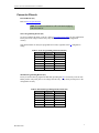
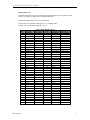
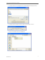
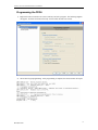
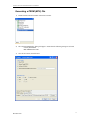
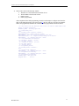
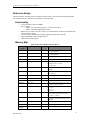
FreeForm/PCI-104
User Manual
Connect Tech, Inc.
42 Arrow Road
Guelph, Ontario
Canada, N1K 1S6
Tel: 519-836-1291
800-426-8979
Fax: 519-836-4878
Email: [email protected]
[email protected]
URL: http://www.connecttech.com
CTIM-00040 Revision 0.00 January 28, 2008
Connect Tech FreeForm/PCI-104 User Manual
Limited Lifetime Warranty
Connect Tech Inc. provides a Lifetime Warranty for all Connect Tech Inc. products. Should
this product, in Connect Tech Inc.'s opinion, fail to be in good working order during the
warranty period, Connect Tech Inc. will, at its option, repair or replace this product at no
charge, provided that the product has not been subjected to abuse, misuse, accident, disaster or
non Connect Tech Inc. authorized modification or repair.
You may obtain warranty service by delivering this product to an authorized Connect Tech
Inc. business partner or to Connect Tech Inc. along with proof of purchase. Product returned to
Connect Tech Inc. must be pre-authorized by Connect Tech Inc. with an RMA (Return
Material Authorization) number marked on the outside of the package and sent prepaid,
insured and packaged for safe shipment. Connect Tech Inc. will return this product by prepaid
ground shipment service.
The Connect Tech Inc. Lifetime Warranty is defined as the serviceable life of the product. This
is defined as the period during which all components are available. Should the product prove to
be irreparable, Connect Tech Inc. reserves the right to substitute an equivalent product if
available or to retract Lifetime Warranty if no replacement is available.
The above warranty is the only warranty authorized by Connect Tech Inc. Under no
circumstances will Connect Tech Inc. be liable in any way for any damages, including any lost
profits, lost savings or other incidental or consequential damages arising out of the use of, or
inability to use such product.
Copyright Notice
The information contained in this document is subject to change without notice. Connect Tech
Inc. shall not be liable for errors contained herein or for incidental consequential damages in
connection with the furnishing, performance, or use of this material. This document contains
proprietary information that is protected by copyright. All rights are reserved. No part of this
document may be photocopied, reproduced, or translated to another language without the prior
written consent of Connect Tech, Inc.
Copyright © 2008 by Connect Tech, Inc.
Trademark Acknowledgment
Connect Tech, Inc. acknowledges all trademarks, registered trademarks and/or copyrights
referred to in this document as the property of their respective owners.
Not listing all possible trademarks or copyright acknowledgments does not constitute a lack of
acknowledgment to the rightful owners of the trademarks and copyrights mentioned in this
document.
Revision 0.00
2
Connect Tech FreeForm/PCI-104 User Manual
Customer Support Overview
If you experience difficulties after reading the manual and/or using the product, contact the
Connect Tech reseller from which you purchased the product. In most cases the reseller can
help you with product installation and difficulties.
In the event that the reseller is unable to resolve your problem, our highly qualified support
staff can assist you. Our support section is available 24 hours a day, seven days a week on our
website at:
www.connecttech.com/support/support.asp. See the contact information section below for
more information on how to contact us directly. Our technical support is always free.
Not listing all possible trademarks or copyright acknowledgments does not constitute a lack of
acknowledgment to the rightful owners of the trademarks and copyrights mentioned in this
document.
Contact Information
We offer three ways for you to contact us:
Telephone/Facsimile
Technical Support representatives are ready to answer your call Monday through Friday, from
8:30 a.m. to 5:00 p.m. Eastern Standard Time. Our numbers for calls are:
Telephone:
Telephone:
Facsimile:
800-426-8979 (North America only)
519-836-1291 (Live assistance available 8:30 a.m. to 5:00 p.m. EST, Monday to
Friday)
519-836-4878 (on-line 24 hours)
Email/Internet
You may contact us through the Internet. Our email and URL addresses are:
[email protected]
[email protected]
www.connecttech.com
Mail/Courier
You may contact us by letter and our mailing address for correspondence is:
Connect Tech, Inc.
42 Arrow Road
Guelph, Ontario
Canada N1K 1S6
Revision 0.00
3
Connect Tech FreeForm/PCI-104 User Manual
Table of Contents
Limited Lifetime Warranty......................................................................................................... 2
Copyright Notice ........................................................................................................................ 2
Trademark Acknowledgment ..................................................................................................... 2
Customer Support Overview ...................................................................................................... 3
Contact Information ........................................................................................................... 3
Table of Contents ....................................................................................................................... 4
List of Tables.............................................................................................................................. 5
List of Figures ............................................................................................................................ 5
Introduction ................................................................................................................................ 6
Features.............................................................................................................................. 6
Hardware Description and Configuration................................................................................... 8
Jumpers and Switches ........................................................................................................ 8
Slot Selection (RSW1) .............................................................................................. 8
FPGA Configuration Settings (J1) ............................................................................ 8
Connector Pinouts.............................................................................................................. 9
PCI-104 Header (P1) ................................................................................................. 9
JTAG Programming Header (P2).............................................................................. 9
SPI Flash Programming Header (P3) ........................................................................ 9
RS-485 Headers (P5, P6)......................................................................................... 10
External Power Connector (P8)............................................................................... 10
GPIO Header (P7) ................................................................................................... 11
Hardware Installation ............................................................................................................... 12
Standalone Operation....................................................................................................... 12
Software Installation................................................................................................................. 12
FPGA Development Environment ................................................................................... 12
Drivers and Application Examples .................................................................................. 12
FPGA Configuration ................................................................................................................ 13
Launch Impact ................................................................................................................. 13
Programming the FPGA .................................................................................................. 16
Generating a PROM (MCS) File ..................................................................................... 17
Configuring the FPGA with the SPI Flash....................................................................... 20
Configuring the FPGA / SPI flash Association ....................................................... 20
Programming the Flash ........................................................................................... 22
Reference Design ..................................................................................................................... 24
Functionality .................................................................................................................... 24
Memory Map ................................................................................................................... 24
Implementation ................................................................................................................ 25
Specifications ........................................................................................................................... 26
Revision 0.00
4
Connect Tech FreeForm/PCI-104 User Manual
List of Tables
Table 1: FreeForm/PCI-104 Components .................................................................................. 7
Table 2: Slot Selection (RSW1) ................................................................................................. 8
Table 3: FPGA Configuration Settings (J1) ............................................................................... 8
Table 4: JTAG Programming Header Pinout (P2)...................................................................... 9
Table 5: SPI Flash Programming Header Pinout (P3) ................................................................ 9
Table 6: RS-485 Port 1 Pinout (P5).......................................................................................... 10
Table 7: RS-485 Port 2 Pinout (P6).......................................................................................... 10
Table 8: External Power Connector Pinout (P8) ...................................................................... 10
Table 9: GPIO Header Pinout................................................................................................... 11
Table 10: Bar Local Address Space 0 (Bar 2) .......................................................................... 24
Table 11: Local Address Space 1 (Bar 3)................................................................................. 25
List of Figures
Figure 1: FreeForm/PCI-104 Block Diagram............................................................................. 6
Figure 2: FreeForm/PCI-104 Layout .......................................................................................... 7
Figure 3: External Power Connection....................................................................................... 10
Revision 0.00
5
Connect Tech FreeForm/PCI-104 User Manual
Introduction
Connect Tech’s FreeForm/PCI-104 features Xilinx’s Virtex-5 multi-platform FPGA offering users a
flexible, reconfigurable product that also takes advantage of the high bandwidth capabilities of the PCI
bus while communicating with various I/O interfaces.
Features
o
o
o
o
o
o
o
o
o
o
o
o
PCI-104 form factor – 32-Bit/33MHz
Xilinx multi-platform Virtex-5 FPGA with 3 million logic gates
8MB Flash for embedded code storage
Designed for embedded processing using MicroBlaze™
100MHz input clock
128MB DDR2-400 memory
External 5V power connection for stand alone usage
2 x 10/100 Ethernet with modular jacks
2 x RS-485 serial interface
On-board reset switch
64 single ended or 32 LVDS general purpose I/O
Available in industrial temperature range of -40°C to 85°
Figure 1: FreeForm/PCI-104 Block Diagram
Revision 0.00
6
Connect Tech FreeForm/PCI-104 User Manual
Figure 2: FreeForm/PCI-104 Layout
Table 1: FreeForm/PCI-104 Components
Connectors
P1
P2
P3
P5, P6
P7
P8
P9
P10
Jumpers /Switches
RSW1
J1
Components
D1-D4
D5
U4
U5
U10
U11
U12, U13
U14
U15, U16
U17
O1
Revision 0.00
Description
PCI-104 connector
JTAG programming header
SPI flash programming header
RS-485 header
GPIO header
External power header
RJ-45 A
RJ-45 B
Description
Slot selection
FPGA configuration settings
Description
User LEDs
FPGA load complete LED
PLX PCI-local bus bridge
Virtex-5 FPGA
FPGA configuration flash
Embedded code flash
DDR2 memory
Parameter EEPROM
RS-485 transceiver
Dual 10/100 PHY
100MHz oscillator, main clock
7
Connect Tech FreeForm/PCI-104 User Manual
Hardware Description and Configuration
The following sections describe the function of all switches/jumpers and provide details on connector
pinouts.
Jumpers and Switches
Slot Selection (RSW1)
This rotary switch selects a slot position in the PCI-104 stack. When mounting on a PCI adapter
card, ensure slot one is selected.
Table 2: Slot Selection (RSW1)
Position
Slot
0,4
0
1,5
1
2,6
2
3,7
3
FPGA Configuration Settings (J1)
Jumper J1 is used to control FPGA configuration.
Table 3: FPGA Configuration Settings (J1)
FPGA waits for configuration over JTAG, using
the cable it is connected to
FPGA reads configuration from SPI flash
FPGA is tri-state, program flash directly
Revision 0.00
8
Connect Tech FreeForm/PCI-104 User Manual
Connector Pinouts
PCI-104 Header (P1)
Refer to PCI-104 specifications.
Note: P1 must be connected to a PCI-104 stack supplying
both 3.3V and 5V
JTAG Programming Header (P2)
Use P2 to configure the FPGA via JTAG. Refer to Programming the FPGA for more information.
Power pins are for voltage reference only; they do not provide power to the configuration
circuitry.
Note that the FPGA can always be programmed via JTAG, regardless of the J1 configuration
setting.
Table 4: JTAG Programming Header Pinout (P2)
Pin
1
2
3
4
5
6
7
Signal
TRST
TMS
TDI
TDO
TCK
GND
3.3V
Direction
Input
Input
Input
Output
Input
Reference
Reference
SPI Flash Programming Header (P3)
P3 may be used to directly program the SPI flash, providing that J1 is set correctly to the tri-state
FPGA position. The power pins are for voltage reference only. They do not provide power to the
configuration circuitry.
Table 5: SPI Flash Programming Header Pinout (P3)
Pin
Signal
Direction
1
SPI_CSN
Input
2
SPI_MOSI
Input
3
SPI_MISO
Output
4
SPI_CLK
Input
5
GND
Reference
6
3.3V
Reference
Revision 0.00
9
Connect Tech FreeForm/PCI-104 User Manual
RS-485 Headers (P5, P6)
Table 6: RS-485 Port 1 Pinout (P5)
Table 7: RS-485 Port 2 Pinout (P6)
Pin
1
2
3
4
5
6
7
8
9
10
Pin
1
2
3
4
5
6
7
8
9
10
Signal
RXD+1
Direction
Input
RXD-1
Input
TXD+1
Output
TXD-1
Output
GND
power
Signal
RXD+2
Direction
Input
RXD-2
Input
TXD+2
Output
TXD-2
Output
GND
power
External Power Connector (P8)
The external connector provides 5V to the power regulation circuitry. In addition, the power
connector enables the 3.3V regulator and provides VIO to the PCI Bridge.
The external power connector should only be used when the FreeForm/PCI-104 is being
programmed out side of a PCI / PCI-104 system.
Table 8: External Power Connector Pinout (P8)
Pin
1
2
3
4
Signal
5V
3.3 enable (connect to 5V)
VIO (connect to 5V)
GND
Direction
Power
Input
Power
Power
It is recommended that a Connect Tech Inc. FreeForm/PCI-104 power supply is used. Orientation
of the power supply connector is important. Ensure that the clip on the cable aligns with the catch
on P8, as shown below.
Figure 3: External Power Connection
Revision 0.00
10
Connect Tech FreeForm/PCI-104 User Manual
GPIO Header (P7)
The GPIO header has been design such that when in differential mode, the positive (P) and
negative (N) signals are adjacent on a standard ribbon cable.
Note that the GPIO voltage level is set via hardware.
FCG001: has L12 populated, enabling 2.5V I/O, including LVDS
FCG002: has L13 populated, enabling 3.3V I/O
Pin
1
2
3
4
5
6
7
8
9
10
11
12
13
14
15
16
17
18
19
20
21
22
23
24
25
26
27
28
29
30
31
32
33
34
35
36
37
38
39
40
Revision 0.00
Signal
GPION(0)
GPIOP(0)
GPION(1)
GPIOP(1)
GPION(2)
GPIOP(2)
GPION(3)
GPIOP(3)
GND
GND
GPION(4)
GPIOP(4)
GPION(5)
GPIOP(5)
GPION(6)
GPIOP(6)
GPION(7)
GPIOP(7)
GND
GND
GPION(8)
GPIOP(8)
GPION(9)
GPIOP(9)
GPION(10)
GPIOP(10)
GPION(11)
GPIOP(11)
GND
GND
GPION(12)
GPIOP(12)
GPION(13)
GPIOP(13)
GPION(14)
GPIOP(14)
GPION(15)
GPIOP(15)
GND
GND
Table 9: GPIO Header Pinout
Direction
Pin
Signal
Input/Output
41
GPION(16)
Input/Output
42
GPIOP(16)
Input/Output
43
GPION(17)
Input/Output
44
GPIOP(17)
Input/Output
45
GPION(18)
Input/Output
46
GPIOP(18)
Input/Output
47
GPION(19)
Input/Output
48
GPIOP(19)
power
49
GND
Power
50
GND
Input/Output
51
GPION(20)
Input/Output
52
GPIOP(20)
Input/Output
53
GPION(21)
Input/Output
54
GPIOP(21)
Input/Output
55
GPION(22)
Input/Output
56
GPIOP(22)
Input/Output
57
GPION(23)
Input/Output
58
GPIOP(23)
Power
59
GND
Power
60
GND
Input/Output
61
GPION(24)
Input/Output
62
GPIOP(24)
Input/Output
63
GPION(25)
Input/Output
64
GPIOP(25)
Input/Output
65
GPION(26)
Input/Output
66
GPIOP(26)
Input/Output
67
GPION(27)
Input/Output
68
GPIOP(27)
Power
69
GND
Power
70
GND
Input/Output
71
GPION(28)
Input/Output
72
GPIOP(28)
Input/Output
73
GPION(29)
Input/Output
74
GPIOP(29)
Input/Output
75
GPION(30)
Input/Output
76
GPIOP(30)
Input/Output
77
GPION(31)
Input/Output
78
GPIOP(31)
Power
79
GND
power
80
GND
Direction
Input/Output
Input/Output
Input/Output
Input/Output
Input/Output
Input/Output
Input/Output
Input/Output
Power
Power
Input/Output
Input/Output
Input/Output
Input/Output
Input/Output
Input/Output
Input/Output
Input/Output
Power
Power
Input/Output
Input/Output
Input/Output
Input/Output
Input/Output
Input/Output
Input/Output
Input/Output
Power
Power
Input/Output
Input/Output
Input/Output
Input/Output
Input/Output
Input/Output
Input/Output
Input/Output
Power
Power
11
Connect Tech FreeForm/PCI-104 User Manual
Hardware Installation
Before installing the FreeForm/PCI-104 into a PC/104 stack, ensure the following:
o
o
Slot selection properly set using the rotary switch RSW1. Note that the FreeForm/PCI-104
address space consumes 32 bytes.
FPGA configuration jumper J1 is set to read from Flash
Once installed in the system and power is applied, the LED D1 will illuminate to indicate that
FreeForm/PCI-104 is functioning properly.
Standalone Operation
Operating the FreeForm/PCI-104 outside of a PCI-104 stack or a PCI system for extended periods of
time is not recommended. The PCI to local bus bridge (PLX 9056) requires the pull-up / pull-down
resistors provided on a system main board.
Configuring / programming the FreeForm/PCI-104 in standalone mode is acceptable, providing it is not
left powered in that state.
Software Installation
FPGA Development Environment
FreeForm/PCI-104 has been developed with Xilinx WebPACK 9.2, available free of charge at:
http://www.xilinx.com/ise/logic_design_prod/webpack.htm
Drivers and Application Examples
The FreeForm/PCI-104 ships with a CD containing drivers for various operating systems and example
programs to help quickly develop applications. Refer to the CD for installation instructions. For other
operating systems, please check the Connect Tech website’s download zone:
http://www.connecttech.com/asp/Support/DownloadZone.asp
Revision 0.00
12
Connect Tech FreeForm/PCI-104 User Manual
FPGA Configuration
To configure the FPGA via JTAG, connect the JTAG programming cable to P2 ensuring that all JTAG
signals align correctly. It is important to note that P2 also has the TRST signal on pin 1, which is not part
of Xilinx’s Parallel or USB programming cables.
Launch Impact
1) Open iMPACT, and select create a new project
2) Select configure devices using boundary scan. iMPACT will scan the JTAG chain, and identify
three devices. The first device will be the FPGA.
Revision 0.00
13
Connect Tech FreeForm/PCI-104 User Manual
3) A prompt will ask for a new configuration file. Select the bitstream from the project directory.
4) A prompt will ask for a BSDL file for device number 2 (PLX PCI9056). Click Yes.
5) Browse to the bsdl folder and select PCI9056BA.bsd
Revision 0.00
14
Connect Tech FreeForm/PCI-104 User Manual
6) iMPACT will add the device to the JTAG chain.
7) Again, a prompt will ask for device number three (National PHY). Browse to the bsdl folder and
select DP83849IVS.bsd. The device will be added to the JTAG chain.
8) To test stream integrity, right click on the FPGA and select Get Device ID. The console will
report IDCODE = 82a6e093
Revision 0.00
15
Connect Tech FreeForm/PCI-104 User Manual
Programming the FPGA
1) Right click on device number one (Virtex-5 FPGA), and select program. The following diagram
will appear. Note that verification will only work if an msk file has been created.
2) Select OK to begin programming. After programming is complete, the status window will report:
Revision 0.00
16
Connect Tech FreeForm/PCI-104 User Manual
Generating a PROM (MCS) File
1) Double click Prom File Formatter in the Flows window.
2) The “Prepare PROM Files” dialog will appear. Ensure that the following settings are selected:
3rd Party SPI PROM
MSC PROM File Format
3) Give the file a name, and click Next.
Revision 0.00
17
Connect Tech FreeForm/PCI-104 User Manual
4) Select the PROM density (16M) → click Next → click Finish.
5) A prompt will ask to add device to data stream 0. Click OK. Select the bitstream from the project
directory.
Revision 0.00
18
Connect Tech FreeForm/PCI-104 User Manual
6) Click “No” when asked if another device is to be added. Click “OK” to accept the setup.
7) Double Click “Generate File” from the “iMPACT” processes menu. The status will be reported in
the console.
// *** BATCH CMD : setMode -pff
// *** BATCH CMD : setSubmode -pffparallel
// *** BATCH CMD : setAttribute -configdevice -attr fillValue -value "FF"
// *** BATCH CMD : setAttribute -configdevice -attr swapBit -value "true"
// *** BATCH CMD : setAttribute -configdevice -attr fileFormat -value "mcs"
// *** BATCH CMD : setAttribute -configdevice -attr dir -value "UP"
// *** BATCH CMD : setAttribute -configdevice -attr path -value
"C:\Data\Projects\FreeFormPCI104\hardware\logic\init_plx_GPIO25\/"
// *** BATCH CMD : setAttribute -configdevice -attr name -value "init_plx_GPIO25.cs"
Total configuration bit size = 9371136 bits.
Total configuration byte size = 1171392 bytes.
// *** BATCH CMD : setCurrentDesign -version 0
// *** BATCH CMD : generate -spi
Swap bit can only be disabled in Hex file format only.
0x11dfc0 (1171392) bytes loaded up from 0x0
Using user-specified prom size of 2048K
Writing file
"C:\Data\Projects\FreeFormPCI104\hardware\logic\init_plx_GPIO25\//init_plx_GPIO25.mcs"
.
Writing file
"C:\Data\Projects\FreeFormPCI104\hardware\logic\init_plx_GPIO25\//init_plx_GPIO25.prm"
.
Revision 0.00
19
Connect Tech FreeForm/PCI-104 User Manual
Configuring the FPGA with the SPI Flash
In previous Xilinx FPGA configurations, the SPI flash would require programming via 3rd party JTAG
test software or through in-system methods. The following features are new to ISE 9.1/9.2, and are only
available on select FPGAs, including the Virtex-5. Your FreeForm/PCI-104 card featuring the Xilinx
Virtex-5 FPGA includes a standard core to enable programming of BPI and SPI flashes over JTAG.
Configuring the FPGA / SPI flash Association
1) Select “Boundary Scan” from the “Flows” tab.
2) Right click on the FPGA and select “Add SPI Flash…”
Revision 0.00
20
Connect Tech FreeForm/PCI-104 User Manual
3) Browse to the directory containing the previously generated MCS file. Select and click “Open”.
4) The “FPGA SPI Flash Association” window will appear; select “M25P16” (this is the flash device
connected to the FPGA).
5) The flash will be added to the FPGA. Note that this flash is not part of the JTAG chain.
Revision 0.00
21
Connect Tech FreeForm/PCI-104 User Manual
Programming the Flash
1) Right click the previously associated flash device, and select program.
2) The programming dialog will appear. Select “Verify” and “Erase Before Programming”, then
click OK.
Revision 0.00
22
Connect Tech FreeForm/PCI-104 User Manual
3) Observe the results in the transcript window.
a. The SPI core is first download to the FPGA device
b. The IDCODE is checked and verified
c. Flash is erased
d. Flash is programmed
After completion of the flash programming, the FPGA will attempt to configure itself from the
flash. If the SPI flash setting is not selected with J1; this step will fail. This does not mean the
flash is not programmed, but rather the verification of the programmed contents has failed.
'1': SPI access core not detected. SPI access core will be downloaded to the
device to enable operations.
PROGRESS_START - Starting Operation.
'1': Downloading core...
done.
'1': Reading status register contents...
INFO:iMPACT:2219 - Status register values:
INFO:iMPACT - 0011 1111 1001 1110 0000 1010 1000 0000
INFO:iMPACT:2492 - '1': Completed downloading core to device.
INFO:iMPACT - '1': Checking done pin....done.
'1': Core downloaded successfully.
'1': IDCODE is '202015' (in hex).
'1': ID Check passed.
'1': IDCODE is '202015' (in hex).
'1': ID Check passed.
'1': Erasing Device.
'1': Programming Device.
'1': Reading device contents...
done.
'1': Verification completed.
INFO:iMPACT - '1': Checking done pin....done.
'1': Programmed successfully.
INFO:iMPACT - '1': Checking done pin....done.
'1': Programmed successfully.
PROGRESS_END - End Operation.
Elapsed time =
179 sec.
Revision 0.00
23
Connect Tech FreeForm/PCI-104 User Manual
Reference Design
The FreeForm/PCI-104 ships with a pre-installed reference design. This reference design demonstrates
how the FPGA interacts with the PLX 9056 PLX to local bus bridge.
Functionality
o
o
o
o
o
o
Local bus interface driven at 50MHz
Slave access to:
o BAR2: 16x32 bit control registers , 16x32 bit user memory
o BAR3: SPI flash programming interface
Master access to same 16x32 user memory as located in BAR2. Transfer controlled through
slave accessible registers.
Local bus master configuration of bridge (happens automatically with reset).
Single-ended GPIO control through registers.
LED control through registers.
Memory Map
Table 10: Bar Local Address Space 0 (Bar 2)
Local Address
(HEX)
Contents
Access
Description
00000000
INTERRUPT_MASK
R/W
Bit 0: Direct master state machine
Bit 1: SPI programmer
00000004
INTERRUPT_SOURCE
R
Bit 0: Direct master state machine
Bit 1: SPI programmer
00000008
REG2
R/W
UNUSED
0000000C
REG3
R/W
UNUSED
00000010
GPIO_P_OUT
W
Each bit corresponds to one GPIO pin output.
Direction must be set to output
00000014
GPIO_P_TRI
W
Each bit corresponds to one GPIO pin direction
(1=Output)
00000018
GPIO_P_IN
R
Each bit corresponds to one GPIO pin input
0000001C
GPIO_N_OUT
W
Same as GPIO_N_OUT
00000020
GPIO_N_TRI
W
Same as GPIO_N_TRI
00000024
GPIO_N_IN
R
Same as GPIO_N_IN
00000028
DM_STATE
R
Bits correspond to direct master states, refer to
plx32master.vhd for more details
0000002C
USER_LED
W
Bit 0: Led 1
Bit 1: Led 2
Bit 2: Led 3
Bit 3: Led 4
00000030
DM_CTRL
W
Bit 0: start operation, when complete must be
cleared before another operation can begin
Bit 1: Write = 1, Read = 0
00000034
DM_ADDR
W
Local bus destination address. Must match what
is programmed into PLX configuration register
DMLBAM.
00000038
DM_CNT
W
Number of DWORDs to transfer
0000003C
REVISION
R/W
Reference design revision
R/W
User Memory
Bit #: GPIO_P(#)
Bit #: GPIO_P(#)
00000040 –
0000007C
Revision 0.00
24
Connect Tech FreeForm/PCI-104 User Manual
Table 11: Local Address Space 1 (Bar 3)
Local Address
Contents
Access
Description
10000000
SPI Command
RW
SPI controller command register, once command is written
operation begins
10000004
SPI Parameters
RW
There are four parameters, each one byte
- 0x04: Param0
- 0x05: Param1
- 0x06: Param2
- 0x07: Param3
10000008
SPI Status
R
SPI controller status register
- Bit 0: Operation complete
1000000C
SPI Result
R
There are four results, each one byte
- 0x04: Result0
- 0x05: Result1
- 0x06: Result2
- 0x07: Result3
10000010 –
100000FC
Un addressable
N/A
N/A
10000100 –
100001FC
Dual port memory RW
256 Bytes of for flash page storage
Implementation
Refer to the FreeForm/PCI-104 VHDL Reference Design Application Note for further information.
Revision 0.00
25
Connect Tech FreeForm/PCI-104 User Manual
Specifications
Programmable FPGA
Virtex-5 FPGA LX30T
Input Clock
100MHz
Memory
8MB Flash, 128MB DDR2-400
General Purpose User I/O 64 single ended I/O
32 LVDS I/O
Serial
2 x RS-485
Ethernet
2 x 10Base-T, 100Base-TX
Operating Environment
Storage Temperature:
-65°C to 150°C
Operating Temperature:
0°C to 70°C
-40°C to 85°C
Power Requirements
(commercial)
(industrial)
+3.3V DC and +5V DC, in PCI-104 stack
+5V DC standalone
Current requirements are configuration dependant
Dimensions
PC/104-Plus 2.2 compliant
PCI-104 1.0 compliant
Connectors
Two RJ-45 modular jacks (Ethernet)
Two 2x5 0.100” headers (serial)
One 2x40 0.050 x 0.100” header (general I/O)
One 1x6 0.100” header (flash programming)
Revision 0.00
26