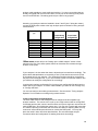
1
FuturePlus® Systems Corporation DDR SDRAM Analysis Probe FS2331 Users Manual For use with Agilent Technologies Logic Analyzers Revision 1.4 FuturePlus is a trademark of FuturePlus Systems Corporation Copyright 2003 FuturePlus Systems Corporation How to reach us.......................................................................................................................4 Product Warranty....................................................................................................................5 Limitation of warranty ...................................................................................................................5 Exclusive Remedies .........................................................................................................................5 Assistance .........................................................................................................................................5 Introduction.............................................................................................................................6 Definitions ........................................................................................................................................6 DDR Bus Speed...........................................................................................................................................6 Probe Cable, Connector Numbering.........................................................................................................6 Logic Analyzer Modules.............................................................................................................................6 Logic Analyzer Machines...........................................................................................................................6 FS2331 Probe Description......................................................................................................8 Probe Feature Summary.................................................................................................................8 Probe Components ..........................................................................................................................8 Probe Design ....................................................................................................................................9 State Clock Generation ...................................................................................................................9 DDR Commands .........................................................................................................................................9 DDR Data ....................................................................................................................................................9 Probe Pod Assignment ..................................................................................................................11 Probe Switch Settings....................................................................................................................12 Logic Analyzer Signal Threshold Voltage Settings ....................................................................13 Connecting the Probe to the Logic Analyzer ..............................................................................13 Connecting Power to the FS2331 Probe ......................................................................................13 Card Requirements for PC2700 Systems ....................................................................................14 Logic Analyzer Card Requirements ............................................................................................15 Software Requirements.................................................................................................................16 System Software........................................................................................................................................16 Setting up the 167xx Analyzer .................................................................................................................16 Setting up the 169xx Analyzer .................................................................................................................16 169xx Licensing.........................................................................................................................................16 Loading 169xx configuration files and define probes feature...............................................................16 Configuration Files........................................................................................................................17 Timing Analysis (All DDR speeds and supported analyzer cards).......................................................17 3 card Configurations for State Analysis................................................................................................18 Probing multiple DDR busses – Interleaved memory................................................................19 Connecting to your Target System – Chip Select .......................................................................20 Chip Select Jumpers .................................................................................................................................20 1) Wiring Chip Select from a DIMM module to the FS2331 .....................................................................20 2) Dedicating a DIMM slot to the FS2331 .................................................................................................21 3) FS1024 or FS1025 Interposer.................................................................................................................23 2 Unused Pods...................................................................................................................................23 Offline Analysis .............................................................................................................................24 Filtering ..........................................................................................................................................25 Timing Analysis Operation...................................................................................................26 Loading the Inverse Assembler and Decoding DDR Commands .............................................26 Taking a Trace, Triggering, and Seeing Measurement Results ................................................26 State Analysis Operation.......................................................................................................26 Minimizing intermodule skew......................................................................................................26 The Inverse Assembler and Decoding DDR Commands ...........................................................27 Taking a Trace, Triggering, and Seeing Measurement Results ................................................27 Tracing the Serial Presence Detect Signals .........................................................................28 Using Eye Finder with the FS2331 DDR Probe..................................................................29 Using EyeScan with the FS2331 Probe ...............................................................................30 Using the FS2331 DDR Probe with an Interposer (FS1024/25) ................................................31 DIMM Signal Loading Option .....................................................................................................31 FS2331 Calibration .......................................................................................................................32 Step 1 – Set Command sample position ..................................................................................................34 Step 2 – Write Burst Data Valid Position ...............................................................................................37 Step 3 – Read Burst Data Valid Position ................................................................................................41 Step 4 – Adjust the delay line value to maximize R/W overlap ............................................................45 Step 5 – Set the final analyzer sample position ......................................................................................45 General Information .............................................................................................................47 Probe Interface design capability............................................................................................................47 Standards supported ................................................................................................................................47 Power requirements..................................................................................................................................47 Logic Analyzer Requirements .................................................................................................................47 Minimum Clock Period............................................................................................................................47 Signal Loading ..........................................................................................................................................47 Environmental Operating Limits ............................................................................................................47 Servicing ....................................................................................................................................................47 Signal Connections ...............................................................................................................48 3 How to reach us For Technical Support: FuturePlus Systems Corporation 15 Constitution Drive Bedford, NH 03110 TEL:603-471-2734 FAX:603-471-2738 On the Web: www.futureplus.com For Sales and Marketing Support: TEL:719-278-3540 FAX:719-278-9586 On the Web: www.futureplus.com FuturePlus Systems is represented in Japan by: ANDOR Systems Support Co., LTD. 15-8, Minami-Shinagawa, 2-chome, Shinagawa-ku Tokyo 140 TEL:03-450-8101 FAX:03-450-8410 Contact : Mr. Takashi Ugajin Outside of Japan, FuturePlus Systems is represented world wide by Agilent Technologies. Please contact your nearest Agilent Sales office. 4 Product Warranty Due to the complex nature of the FS2331 and the wide variety of possible customer target implementations, the FS2331 has a 30 day acceptance period by the customer from the date of receipt. If the customer does not contact FuturePlus Systems within 30 days of the receipt of the product it will be said that the customer has accepted the product. If the customer is not satisfied with the FS2331 they may return the FS2331 within 30 days for a refund. This FuturePlus Systems product has a warranty against defects in material and workmanship for a period of 1 year from the date of shipment. During the warranty period, FuturePlus Systems will, at its option, either replace or repair products proven to be defective. For warranty service or repair, this product must be returned to the factory. For products returned to FuturePlus Systems for warranty service, the Buyer shall prepay shipping charges to FuturePlus Systems and FuturePlus Systems shall pay shipping charges to return the product to the Buyer. However, the Buyer shall pay all shipping charges, duties, and taxes for products returned to FuturePlus Systems from another country. FuturePlus Systems warrants that its software and hardware designated by FuturePlus Systems for use with an instrument will execute its programming instructions when properly installed on that instrument. FuturePlus Systems does not warrant that the operation of the hardware or software will be uninterrupted or error-free. Limitation of warranty The foregoing warranty shall not apply to defects resulting from improper or inadequate maintenance by the Buyer, Buyer-supplied software or interfacing, unauthorized modification or misuse, operation outside of the environmental specifications for the product, or improper site preparation or maintenance. NO OTHER WARRANTY IS EXPRESSED OR IMPLIED. FUTUREPLUS SYSTEMS SPECIFICALLY DISCLAIMS THE IMPLIED WARRANTIES OF MERCHANTABILITY AND FITNESS FOR A PARTICULAR PURPOSE. Exclusive Remedies THE REMEDIES PROVIDED HEREIN ARE BUYER’S SOLE AND EXCLUSIVE REMEDIES. FUTUREPLUS SYSTEMS SHALL NOT BE LIABLE FOR ANY DIRECT, INDIRECT, SPECIAL, INCIDENTAL, OR CONSEQUENTIAL DAMAGES, WHETHER BASED ON CONTRACT, TORT, OR ANY OTHER LEGAL THEORY. Product maintenance agreements and other customer assistance agreements are available for FuturePlus Systems products. For assistance, contact the factory. 5 Introduction Thank you for purchasing the FuturePlus Systems FS2331 DDR SDRAM Logic Analyzer Probe. We believe you will find the FS2331, along with your Agilent Technologies Logic Analyzer, a valuable tool for helping to characterize and debug your DDR-based systems. This User Manual will provide the information you need to install, configure, and use the FS2331 Probe. If you have any questions about this User Manual or use of the FS2331 Probe, please contact FuturePlus Systems Corporation. Definitions DDR Bus Speed This document will use the following definitions when describing DDR memory speeds: • PC1600 or 200Mhz describes DDR DIMMs running at a clock rate on the memory bus differential clock of 100Mhz, which results in a data transfer rate of 200Mhz (or 1.6 GBytes/sec throughput). DDR commands are issued at a 100Mhz rate. • PC2100 or 266Mhz describes DDR DIMMs running at a clock rate on the memory bus differential clock of 133Mhz, which results in a data transfer rate of 266Mhz (or 2.1 GBytes/sec throughput). DDR commands are issued at a 133Mhz rate. • PC2700 or 333Mhz describes DDR DIMMs running at a clock rate on the memory bus differential clock of 167Mhz, which results in a data transfer rate of 333Mhz (or 2.7 GBytes/sec throughput). DDR commands are issued at a 167Mhz rate. Probe Cable, Connector Numbering The FS2331 has 4 connectors that connect to the logic analyzer through 4 logic analyzer adapter cables. These connectors are described as "J1" through "J4". When "Pod <n>" is referenced in this manual it is the logic analyzer cable end that is plugged into "J <n>" of the FS2331 per figure on page 7. Logic Analyzer Modules "Module" - A set of logic analyzer cards that have been configured (via internal cables connecting the cards) to operate as a single logic analyzer whose total available channels is the sum of the channels on each card. A trigger within a module can be specified using all of the channels of that module. Each module may be further broken up into "Machines”. A single module may not extend beyond a single 5 card frame. Logic Analyzer Machines "Machine" - A set of logic analyzer pods from a logic analyzer module grouped together to operate as a single state or timing analyzer. Each logic analyzer module may be partitioned into up to two independent "Machines" (either two state machines, or a state and a timing machine), and the pods of a module may be assigned freely to either machine. Each state analyzer machine has its own state clock. Turbo mode (333Mhz for 1671x, 400Mhz for 16750/1/2, 600Mhz for 16753/4/5 cards) operation restricts a module to having only one machine. Cross triggering between modules or machines is done via the Intermodule Bus or via the Flag bits, which will communicate across a 16700 frame and its expander, or across multiple frames if the Multiframe product is used. 6 FS2331 100 pin Connector to Pod Diagram Four 100 pin SAMTEC connectors on the FS2331 Four - E5385A or E5378A adapter cables connecting to the logic analyzer POD 1 (odd) J1 POD 2 POD 3 (odd) J2 POD 4 POD 5 (odd) J3 POD 6 POD 7 (odd) J4 POD 8 E5385A adapter cables (FS1015) are used to connect to the following logic analyzer cards: 1671X, 16750/1/2/3 E5378A adapter cables (FS1014) are used to connect to the following logic analyzer cards: 1676X, 16754/5/6 7 FS2331 Probe Description The FS2331 DDR DIMM Probe allows you to perform state and timing analysis measurements on Double Data Rate DRAM DIMM busses using an Agilent logic analyzer. Probe Feature Summary • Quick and easy connection between the DDR 184 pin DIMM connector and Agilent Logic Analyzers. • Complete and accurate state analysis up to 333Mhz (PC2700). • Complete and accurate 4 GHz timing analysis. • Compatible with all 184-pin, 2.5V DDR SDRAM DIMM's up to 333 MHz. • Built-in support for probing Chip Select lines of other DIMM slots. • Data groups and their strobes matched to better than 50ps, address and commands matched to better than 180ps. • All signals are provided to the logic analyzer unbuffered. • Registered and non-registered DIMMS are supported. • User configurable capacitor pads allow modeling of 1, 2, and 4 rank (stacked) DIMMS for signal integrity validation with EyeScan. • DDR Commands are always visible. Switches select state analysis acquisition of data writes only, reads only, or both writes and reads. • Uses Agilent "Eye Finder" technology to locate tight DDR data valid windows for optimal state data capture and to help identify bus signals with marginal timing needing closer examination. • Probe can be used with Agilent EyeScan technology to provide eye diagram of DDR and address/command signals. • Both x4 and x8 SDRAMS are supported. • Read and write burst type is tracked in real time and each cycle of a burst (in both state and timing mode) is sent to the analyzer. Probe Components The following components have been shipped with your FS2331 DDR Probe: • FS2331 DDR DIMM Probe with 3 extra jumpers and 1700 ps delay line. • Dedicated power supply for the FS2331 probe. • Floppy disk(s) with inverse assembler and configuration files for 167xx. • CD with inverse assembler and configuration files for 169xx • This User Manual on CD. • Quick Start Sheet. • Software Entitlement Certificate. This is for 169xx or Off-Line Analysis only. 8 Probe Design This probe uses discrete ECL logic in order to operate at the speed necessary to provide DDR333 signal decode. Because ECL logic operates in linear mode it dissipates more heat than other logic designs. BE ADVISED – THE PROBE IS HOT TO THE TOUCH. . If the user believes that the FS2331’s temperature is above 80°C, then a fan should be used to provide additional cooling. In order to support source synchronous data capture the FS2331 DDR probe monitors the clock (CK0/CK0n) and control (DQS0, CAS, RAS, WE, S0:3) signals on the DIMM connector where the probe is inserted. In some cases the probe may also need access to the chip select signals for other DIMM slots to enable source synchronous data capture. There may be situations where these signals are not provided by the target system. For instance, some systems may turn off CK0 to slots where no DIMM module is detected. In other systems, the unique Chip Select signals for each DIMM may need to be connected to the probe. If there is any reason to suspect that these conditions are present on your target, contact FuturePlus Technical Support. State Clock Generation The FS2331 DDR probe uses one logic analyzer machine to capture DDR commands (using the common clock CK0) and another machine to capture DDR burst data (using the source synchronous strobe DQS0). The logic analyzer automatically combines the trace data from both machines into a single time correlated trace of DDR bus activity. The circuitry on the probe is used to generate the proper state analysis clocks for the command and data analysis machines. DDR Commands Since the DDR bus global clock is differential it is converted to a single ended clock for the analyzer using a differential line receiver. DDR Commands are sampled on the rising edge of this clock. DDR Data The FS2331 supports state analysis of DDR busses by combining a specially processed version of the DQS0 strobe with Agilent's Eye Finder technology. This allows the analyzer/probe combination to accurately locate (much as a DDR controller chipset does) the read and write data valid windows for each data bus signal and sample the data at the proper time for reliable state analysis. Each DDR bus implementation will have different timing due to trace length variation on the motherboard, variations in bus loading for each DIMM configuration, and sensitivity to dynamic factors such as crosstalk or simultaneous switching noise. Therefore, the precise position of the DDR data eye will vary from system to system and even within a system as DIMM configurations or data access patterns change. To achieve the most reliable data capture the location of the data eye must be determined on a given system using worst case data access patterns. The logic analyzers Eye Finder feature is used to measure the location of the eye for each data signal over millions of burst cycles and so achieve the most reliable state capture. By using the proper stimulus when running Eye Finder the worst-case data valid window boundaries are found and the analyzer is set to sample data at the center of the actual data valid window of each signal for each specific DDR implementation and DIMM configuration. 9 Because strobe edges are centered on the data valid window for writes, and straddle it for reads, the analyzer cannot simply use the raw DQS0 to sample data. If it did, then even in the ideal case, only half of the data valid window would be usable. In practice, it would almost completely disappear. To deal with this, the DDR Probe adjusts the timing of DQS0 before sending it to the analyzer state clock input by delaying it a fixed amount for reads. This is done using a socketed delay line, which is set at the factory and should be sufficient. If EyeFinder results show good eyes when the probe is set to pass Reads only and Writes only (SW #6 off), but the eyes are significantly reduced when the probe passes BOTH Reads and Writes (SW #6 on), then the delay value on the probe may need adjustment. The calibration procedure documented in this User Manual describes how to set the probe delay line and analyzer sample position for reliable state analysis operation. Because the strobes are tristated between bursts their logic value is undefined. Some systems will terminate the DDR bus to a voltage close to the Vref voltage, causing the strobes to sit right at the switching threshold. During read bursts, because read data (and strobes) are actually not valid until the reflected wave reaches the probe, DQS0 may also spend a significant amount of time at Voh/2 (close to Vref) between arrival of the incident wave and the reflected wave. Therefore, simply comparing the DQS0 signal to Vref will result in spurious analysis clocks being generated between bursts and during read bursts. The DDR probe deals with these factors by recognizing valid DQS0 edges only when they are closer to Vih than Vref as well as by inhibiting the state clock between bursts. In actual operation enough noise immunity is added by the special DQS0 receiver circuit to eliminate almost all spurious data strobes without inhibiting the clock. All of these factors combine to add jitter to the read and write strobes sensed by the DDR probe. This jitter reduces the data valid window available to the logic analyzer. In some systems and DIMM configurations that have tight bus timing this may make it difficult to find an appropriate point to sample state data. This is especially true for read bursts that usually have more complex strobe and data waveforms. Eye Finder will measure the data valid window available to the analyzer for each signal and clearly indicate which ones may have difficulty reliably sampling state data given actual DDR bus timing. 10 Probe Pod Assignment The FS2331 DDR Probe uses 8 pods. Two are used to capture traffic on the DDR Command bus, and 6 are used for the Data bus, strobes, check bits, masks, and Serial Presence Detect signals. The signals are mapped to pods as follows: Pod 1 Odd 2 Even 3 Odd 4 Even Clock Domain (Clock Rate) Data (2x) State Analysis Clock (on JCLK), DQ0-3, DQ8-11, DQ16-19, DQS0-2, SA0 Data (2x) Read/Write status (on KCLK), DQ4-7, DQ12-15, DQ20-23, DQS9-11, SA1 Data (2x) Burst Valid status (on JCLK), CB0-5, DQ24-31, DQS3, DQS12 Command (1x) CK0 (on KCLK), A0-15 Command (1x) Buffered Command Clock (on JCLK), BA0-2, S03, CKE0-1, WE, RAS, CAS, Reset, FETEN. Spare Data (2x) Buffered Command Clock (on KCLK), CB6-7, SA2, WP, DQS4, 8, 13, 17. DQ32-39. Data (2x) (Spare – J10on JCLK), SDA, DQS5-7, DQ40-43, DQ48-51, DQ56-59 Data (2x) (Spare – J11on JCLK), SCL, DQS14-16, DQ4447, DQ52-55, DQ60-63. 5 Odd 6 Even 7 Odd 8 Even SIGNAL GROUP The overlap in the bit ranges for signals between pods occurs because the bits are assigned to pods in the order that they appear physically on the DIMM connector, which is not strictly in logical bit order. This allows the probe layout to better match stub lengths among all DQxx signals. See the Appendix for a detailed list of how Logic Analyzer Channels are mapped to signals and DIMM pins. 11 Probe Switch Settings A switch bank of 6 independent SPST switches is provided on the FS2331 for user selection of a number of probe features. These are detailed below. Switch # Default (factory position) Function 1 Open Not available 2 Open Not available 3 Open Not available Open When SW4 is closed the Buffered Command Clock signal to the logic analyzer is passed only when there is a valid (low) S0:3 signal to the probe. This is useful for EyeScan of Command signals. Open SW5 is dependent on SW6. When SW6 is open, SW5 open will pass a state clock signal only during a Read command. SW5 closed will pass only on a Write. Closed When SW6 is closed, the probe provides a state clock during both Reads and Writes. When SW6 is open it engages SW5. 4 CS_Gate_CK0 5. Write or Read Only 6 R/W Filter ON (closed) 1 2 3 4 5 6 12 Logic Analyzer Signal Threshold Voltage Settings Threshold voltage settings are set at SSTL-2 levels (1.25 V) for all pods in the format specification of the analyzer. The user may have to adjust this setting for optimal performance for their specific target. Eye Finder and/or EyeScan may have to be run to find out if adjusting the threshold levels will optimize the data valid windows. Connecting the Probe to the Logic Analyzer The FS2331 requires two or three logic analyzer cards depending on the DIMM bus speed, whether state or timing measurements are being used, and the type of logic analyzer card being used. For timing measurements only two cards (configured as a single logic analysis module using one analyzer “machine”) are necessary. Whether using a 2 card or a 3 card configuration, the cards must all be the same model. Because the DDR bus clocks commands on one clock and strobes data on a separate set of strobes, state analysis requires that two separate analyzer “machines” be used, one for Commands and one for Data. For 200Mhz operation 16750/1/2 (200/400Mhz) cards provide sufficient speed in their normal mode to capture Data and Commands, so a two card module configured into one machine for Commands and one for Data is sufficient. When running at higher speeds, the analyzer capturing Data bursts may need to be configured to run in its high speed (Turbo) mode, which requires it to be in a module of its own. A third card configured as a separate module is then needed to capture and trigger on DDR Commands. Six pods of the data module are used for data capture (two are reserved for time tags). However, only two pods in the module used to capture DDR Commands are used for Command capture. The other two may be used for any other purpose (such as to probe chip select signals of a separate DDR memory bank). If 16760 cards are being used for both Command and Data analyzers, then 5 cards are required. One card for commands, 4 cards for data. The reason 4 cards are required for data, is because the cards must be run in 400 Mb/s mode with time tags turned on for time correlation with the Command machine; with time tags turned on 1 pod per machine cannot be used. With 4 cards connected together as one machine with time tags on at 400 Mb/s or greater there are 7 pods out of 8 available to use. th Without the 4 card only 5 pods would be available, when 6 are needed. A summary of this information appears on the following table. Triggering on a combination of commands and data is accomplished by using the Intermodule Bus, which sends an "Arm" signal between all analyzer modules. You can also use the "Flag" bits to communicate between the DDR Command and DDR Data triggering systems. Connecting Power to the FS2331 Probe After connecting the probe to the logic analyzer cables, insert it into the target system. After the probe is in the target system and connected to the logic analyzer, connect the external power supply provided with the FS2331 to the probe. Do this step last and only use the power supply provided with the FS2331. 13 Card Requirements for PC2700 Systems In order to insure that the FS2331 and the logic analyzer work properly with PC2700 systems it is recommended that the 16753/4/5/6 cards be used when probing at DDR rates of 333Mhz or greater. This recommendation is based on several factors. First, the setup and hold requirement for PC2700 is specified as a minimum of 900 ps. Some combination of target systems and DIMMs may operate with a setup and hold time greater than this, but to insure accurate data capture the higher performance of the 16753/4/5/6 cards is needed. Second, the loading on the target system presented by the 16753/4/5/6 combined with the E5378A adapter cables is significantly lower than the loading of the 1671x or 16750/1/2 and the E5385A cables. This may affect target system performance or measurements. 14 Logic Analyzer Card Requirements DDR Bus Speed 200MHz (PC1600) 266MHz (PC2100) 16700 Analyzer Type Timing Analysis State Analysis 16717/8/9 2 cards configured as one module with one timing machine 1675X 2 cards configured as one module with one timing machine 3 cards: • 1 card module with one 167Mhz state machine for Commands • 2 card module with one 333Mhz state machine for Data 2 cards configured into one module having two 200Mhz machines, one with 2 pods for commands, one with 6 pods for Data. 16717/8/9 2 cards configured as one module, one machine 3 cards: • 1 card module with one 167Mhz state machine for Commands • 2 card module with one 333Mhz state machine for Data 1675X 2 cards configured as one module, one machine 3 cards: • 1 card module with one 200Mhz state machine for Commands 2 card module with one • 400Mhz state machine for Data 16760 4 cards configured as one module, one machine 5 cards: § • 333MHz (PC2700) 15 16753/4/5/6 recommended 2 cards configured as one module, one machine 1 card module at 200 Mb/s for commands. 4 card module at 400 Mb/s for Data. 3 cards: • 1 card module with one 200Mhz state machine for Commands • 2 card module with one 400Mhz state machine for Data Software Requirements System Software The FS2331 Probe requires version A.02.70.00 (or later) of the 16700 System Operating Software. You can check to see if you already have the correct version by opening the “System Administration” dialog and selecting the “Show Version” button. If you do not have the correct version then you must update your system software. Please consult 16700 system documentation for the SW update procedure. Setting up the 167xx Analyzer The floppy disk(s) supplied with the FS2331 DDR Probe contains the software required to operate the FS2331. Install the Inverse Assembler and Configuration files from the floppy using the 16700 software installation procedure. This will install an inverse assembler called “IFS2331E” in the standard location for inverse assemblers, and will install several configuration files in the /logic/configs/FuturePlus/FS2331 directory that allow you to easily configure the analyzer for timing or state operation with the FS2331. See the sections below for information on which configuration file to use for your application. Setting up the 169xx Analyzer A CD containing the 16900 software is included in the FS2331 package. The CD contains a setup file that will automatically install the configuration files and protocol decoder onto a PC containing the 16900 operating system or onto a 16900 analyzer itself. To install the software simply double click the .exe file on the CD containing the 16900 software. After accepting the license agreement the software should install within a couple of minutes. 169xx Licensing Once the software has been successfully installed you must license the software. Please refer to the entitlement certificate for instructions on licensing the software. The software can only be installed on one machine. If you need to install the software on more than one machine you must contact the FuturePlus sales department to purchase additional licenses. Loading 169xx configuration files and define probes feature When the software has been licensed you should be ready to load a configuration file. You can access the configuration files by clicking on the folder that was placed on the desktop. When you click on the folder it should open up to display all the configuration files to choose from. If you put your mouse cursor on the name of the file a description will appear telling you what the setup consists of, once you choose the configuration file that is appropriate for your configuration the 169xx operating system should execute. The protocol decoder automatically loads when the configuration file is loaded. If the decoder does not load, you may load it by selecting tools from the menu bar at the top of the screen and select the decoder from the list. After loading the configuration file of choice, go into the format specification of the configuration by choosing Setup from the menu bar and then selecting Bus/Signal in the drop down menu. When the format specification appears press Define Probes at the bottom of the screen. The Define Probes feature will describe how to hook the analyzer cards to the connections on the target. The following figure shows what the Define Probes screen looks like. The figure below may differ from your display; this is an example of how the display looks in general. 16 Note: In the above picture under Logic analyzer pods, the first pod goes to the Odd pod and the second goes to the Even pod of the termination adapter (e.g. Pod B1 goes to odd termination adapter pod and B2 goes to the even termination adapter pod). Configuration Files 167xx Analyzer 169xx Analyzer State/Timing Comment 16717/8/9, 1675x 1675x, 1695x, 1691x DR231_1 2 card timing 16717/8/9, 1675x 1675x, 1695x, 1691x DR231_2 3 card state analysis DR231_3 Two Interleaved DDR Banks, 5 cards required 16717/8/9, 1675x 1675x, 1695x, 1691x Timing Analysis (All DDR speeds and supported analyzer cards) For timing analysis operation you need only two cards (except for the 16760, which requires four) regardless of supported card type or bus speed. These must be configured via the cables supplied with the cards as a single logic analyzer module. Refer to the appropriate Agilent Technologies manual for information on how to connect 17 analyzer cards together to create multi-card modules. You may use modules that are already configured with more than two cards, but only two of the cards (8 pods) will be used for each DDR bus. Remaining pods may be used for any purpose. Assuming your analyzer cards are installed in slots C and D (slot C being the master), connect the DDR probe cables to the logic analyzer pods as follows for timing analysis measurements: FS2331 Conn (J) J1 Odd J1 Even J2 Odd J2 Even J3 Odd J3 Even J4 Odd J4 Even Probe Cable Pod 1 Pod 2 Pod 3 Pod 4 Pod 5 Pod 6 Pod 7 Pod 8 Analyzer Pod Analyzer Pod 2 card timing configuration 3 card state configuration A1 A2 A3 A4 B1 B2 B3 B4 A1 (master 1) A2 B1 C2 (master 2) C1 B2 B3 B4 169xx users please refer to the “Setting up the 16900 Analyzer” section of this manual on the use of the define probes feature to determine how to attach the logic analyzer to the probe If your analyzer is in slots other than these, adjust the pod connections accordingly. The probe cables indicated above as connecting to slot C pods should connect to the pods of the master slot of your analyzer. The remaining pod cables should be connected to the pods of the next higher slot. If you must connect to pods in some other fashion, then you will have to modify the configuration file accordingly. Load the logic analyzer configuration file for timing (see configuration file table) into the master slot of your analyzer. It doesn't matter whether you select to load "Configs only" or "Configs and Data". You are now ready to start making measurements. See the section “Timing Analysis Operation” for information on making timing measurements. 3 card Configurations for State Analysis The three cards used for state analysis must be configured as two separate logic analyzer modules. The card in slot C is set up as a single card module for tracing DDR Commands and the card in slots A and B must be set up as a single two card module for tracing DDR Data. Slot A holds the master card. You may use a module with more than one card for capturing Commands and more than two cards for capturing Data, but only a subset of each modules pods will then be used by the DDR probe. You may also place the cards in slots other than described here, but must then adjust the pod connection tables and configuration file loading instructions accordingly. 18 Load the system config file “DR230_2” for 3 card state. This file will cause all three cards to be configured for state analysis operation. The card in slot C will be setup to capture DDR Commands at the CK0 rate. The full triggering capabilities of the analyzer are available if it is operating in “normal” mode (limit of 167Mhz for 16717 or 200Mhz for 16750/1/2 cards). The cards in slot A and B (slot A is the master card) are configured to capture DDR Data transfers at 2x the CK0 rate. 1671X or 16750/1/2 cards are configured in “Turbo” mode which provides full speed state analysis with reduced triggering capability. You are now ready to start making measurements. See the section “State Analysis Operation” for information on making state measurements. Probing multiple DDR busses – Interleaved memory Interleaved memory is defined here as a memory system that has multiple independent banks of memory in which the selection of the active bank is controlled by the memory address (typically the least significant bits). This allows one bank to initiate a new burst while the other bank is executing a burst. Each bank independently receives and processes its own set of DDR Commands. The DDR probe supports analysis of interleaved memory by allowing you to plug a probe into a slot on each bank. Each probe is connected to independent logic analyzer “machines” using the instructions provided above. Because only two pods on the Command analyzer are used for each bus, you may share the Command analyzer with the second probe, using its two unused pods to independently trace the Command bus on the other memory bank. You still need additional cards to trace the data transfers for the second bank. Thus, to trace two banks of interleaved memory you need 5 cards configured into three separate modules; One card module split into two machines for the DDR Commands of each bank, and two separate two card modules for tracing the two banks DDR Data transfers. Refer to the table on page 17, and load the system config file for interleaved DDR Banks into all. The system config file will configure all five cards. The data burst capture modules are assumed to be in slots A(master) and B, and D(master) and E. The command capture card is assumed to be in slot C, with pods C3 and C4 connected to the DDR bus whose data bus is probed by slots D/E, and pods C1 and C2 are connected to the DDR bus whose data bus is probed by slots A/B. Measurement on more than two banks are supported by replicating this strategy for the additional banks. Up to four banks can be analyzed by a single 16700 mainframe and expander. The following figure shows this setup: DIMM Bank 0 Data 16700 Slot A 16700 Slot B Command C1/2 DIMM Bank 1 Command Data 16700 Slot D 16700 Slot E 19 C3/4 Connecting to your Target System – Chip Select Many DDR333 systems qualify Command activity using the Chip Select lines, S0:3. This is either because they utilize “2T Timing” in which their control lines (RAS, CAS, WE) may not fully transition to a valid state within one command clock, or because NOP commands are indicated only by releasing all chip selects rather than issuing an actual NOP command. Either of these conditions will make it difficult for the FS2331 to decode Commands properly without valid Chip Select signals. Because Chip Select (S0:3) signals are routed independently to each DIMM slot and the FS2331 consumes a slot, the probe will not normally be able to see which memory a given command is directed to. As a result the probe cannot properly decode activity on DIMMs that is qualified by these signals unless they are brought to the probe. On some systems this will be seen as small or missing Data eyes after running Eyefinder . This problem can be corrected if the chip select signals for all memory ranks to be traced are made visible to the probe. The FS2331 user has several means for connecting up to 4 different Chip Select signals to the FS2331. Chip Select Jumpers The factory configuration of the FS2331 is a single jumper on J8 between pins 1 and 2. This forces S0 low (active) on the FS2331 and effectively qualifies ANY Command seen by the FS2331. This may be sufficient for the proper operation in your target system. If it is not, then there are 3 ways to bring active Chip Select signals to the FS2331. Please note that each of these methods requires all jumpers to be removed from J8. 1) Wiring Chip Select from a DIMM module to the FS2331 Four test points are provided on the DDR probe to allow you to probe Chip Selects from other DIMM slots on the target. You must solder a wire from the DIMM module and connect the wire to the appropriate test point on the FS2331. A table showing jumper configurations is provided. GND points are on J8 pins 2, 4, 6, and 8 to allow the use of twisted pairs . You should keep the wires as short as possible. Chip Select line Remove jumper (factory config) Connect wire from another DIMM to If User is dedicating a DIMM slot, or using an Interposer (FS1024 or 1025) add S0 J8 pins 1 and 2 J5 pin 2 Jumper J5 pins 1 and 2 S1 J5 pin 4 Jumper J5 pins 3 and 4 S2 J5 pin 6 Jumper J5 pins 5 and 6 S3 J5 pin 8 Jumper J5 pins 7 and 8 AnyCS (special) J5 pin 10 Jumper J5 pins 9 and 10 20 Factory config is J8 pin 1&2 jumpered. This must be removed if J5 connections are used. Chip Select Jumper locations 2) Dedicating a DIMM slot to the FS2331 This approach offers the highest signal integrity. It involves dedicating a DIMM slot to the FS2331, isolating the Chip Select signals on that DIMM connector from the target’s DDR bus and then wiring active Chip Select signals from all active DIMMs over to the probe’s DIMM connector. Please note that this requires that the appropriate jumpers be placed on J5 per the table above. The following photos detail this wiring process. § Isolate the Dedicated DIMM’s pin. The standard 184 pin DDR DIMM connector has the 4 Chip Select lines routed to the following pins: pin 157 (S0), pin 158 (S1), pin 71 (S2), pin 163 (S3). Most applications will require just S0 single sided DIMMs) or S1 (double-sided DIMMs) to be isolated and jumpered from the active DIMM slot. Identify the correct pin on the dedicated DIMM slot connector and remove the solder from the pin and hole as shown. 21 § Sleeve the Pin Slide a short length of insulation over the exposed connector pin to fully protect it from contacting the barrel of the hole. Insulation from 30 AWG wire is a good fit. 22 § Wire from the adjacent DIMM slot to the isolated pin Using a short length of rework wire connect the adjacent slot’s identical pin, e.g. pin 157 for S0, to the isolated pin on the dedicated DIMM slot. 3) FS1024 or FS1025 Interposer Use of either of these interposers allows a single DIMM slot to support both the FS2331 probe and a DIMM module. The convenience of this approach can be offset by the impact of the additional etch length that the interposer provides. If an FS1024 or 1025 interposer is used, J5 jumpers should be configured per the previous table. This allows the FS2331 to use the Chip Select signals as seen by the DIMM module in the interposer. This does not provide Chip Select signals from any other DIMM slot. Please note that the jumper J10 on the FS2331 has to be removed when the probe is in the interposer in order to reduce loading on CK0. Factory config is J10 jumper installed. Unused Pods Depending on the DDR bus speed being probed and the logic analyzer cards used, there may be unused pods. These pods may be used to trace other signals. You should remember to add the two pods to the machine (using the “Pod Assignment” dialog of the Format tab). You will also need to setup the format spec to map labels to these channels on the DDR probe. 23 Offline Analysis Data that is saved on a 167xx analyzer in fast binary format, or 16900 analyzer data saved as a *.ala file, can be imported into the 1680/90/900 environment for analysis. You can do offline analysis on a PC if you have the 1680/90/900 operating system installed on the PC, if you need this software please contact Agilent. Offline analysis allows a user to be able to analyze a trace offline at a PC so it frees up the analyzer for another person to use the analyzer to capture data. If you have already used the license that was included with your package on a 1680/90/900 analyzer and would like to have the offline analysis feature on a PC you may buy additional licenses, please contact FuturePlus sales department. In order to view decoded data offline, after installing the 1680/90/900 operating system on a PC, you must install the FuturePlus software. Please follow the installation instructions for “Setting up a 16900 analyzer”. Once the FuturePlus software has been installed and licensed follow these steps to import the data and view it. From the desktop, double click on the Agilent logic analyzer icon. When the application comes up there will be a series of questions, answer the first question asking which startup option to use, select Continue Offline. On the analyzer type question, select cancel. When the application comes all the way up you should have a blank screen with a menu bar and tool bar at the top. For data from a 16900 analyzer, open the .ala file using the File, Open menu selections and browse to the desired .ala file. For data from a 16700, choose File -> Import from the menu bar, after selecting import select “yes” when it asks if the system is ready to import 16700 data. 24 After clicking “next” you must browse for the fast binary data file you want to import. Once you have located the file and clicked start import, the data should appear in the listing. After the data has been imported you must load the protocol decoder before you will see any decoding. To load the decoder select Tools from the menu bar, when the drop down menu appears select Inverse Assembler, then choose the name of the decoder for your particular product. The figure below is a general picture; please choose the appropriate decoder for the trace you are working with. After the decoder has loaded, select Preferences from the overview screen and set the preferences to their correct value in order to decode the trace properly. Filtering The offline IA allows filtering just like the 16700/702 environments. You may filter on any label, when using the filter tags label you can select symbols to make choosing transactions easier. To create a filter, choose Tools, New, Filter/Colorize. Then fill in the information on the window that opens up. You must create a new filter for each item you want filtered. It is best to filter out transactions you don’t want on the 16700/702 rather than waiting and filtering on the captured data. To remove filters that you no longer want, go to Tools, Overview and then choose the filter you want removed and press Delete. 25 Timing Analysis Operation Loading the Inverse Assembler and Decoding DDR Commands No Inverse Assembler is used for timing analysis. However, symbols are pre-defined for the DDR Command bus. These decode the RAS, CAS, and WE lines to display the DDR Command as “Read”, “Write”, “Precharge”, etc., so you don’t have to refer to the DDR device data sheet to see what command is being executed. Symbols have also been pre-defined for the Read/Write status generated by the probe. Taking a Trace, Triggering, and Seeing Measurement Results Timing analysis is the simplest setup, and there are no special factors involved in analyzer trigger setup, initiating a trace, and viewing results. For the Command bus you can use the pre-defined symbols to specify mnemonically the command you wish to trigger on. These are set up by default and are accessible in the trigger tab. The default waveform display also shows DDR Commands mnemonically. You may setup a trigger, initiate a measurement, and view results in the usual ways via the trigger tab, pressing the run button, and opening the desired display window. State Analysis Operation The FS2331 DDR Probe supports the simultaneous 200/266/333Mhz DDR state and 2GHz timing measurement capability of the Agilent Logic Analyzers as well as capture of both Read and Write bursts in a single trace. The optional calibration procedure documented at the end of this document applies to state measurements only. You may use the 2GHz TimingZoom feature at any time during state or timing mode measurements. Minimizing intermodule skew The 16700 will automatically time correlate activity on the Command and Data busses. The accuracy of the correlation is typically several nanoseconds, but can be larger. Since even a few nanoseconds is an appreciable fraction of a DDR cycle the DDR Probe provides a mechanism to reduce the skew to approximately one nanosecond using the Intermodule Skew adjustment dialog in the 16700 Intermodule setup window. To minimize the skew between the logic analyzer channels tracing the Command and Data busses a common signal (Buffered Command Clock) is probed by both analyzers. This signal will have identical timing (within 1ns) as measured by TimingZoom when the skew between the Command and Data analyzers is minimized. A detailed procedure to minimize intermodule skew is: 1. Set up the analyzer for state analysis measurements using the procedures described earlier in this User Manual. 2. Make sure that the TimingZoom feature is enabled for both the Command and Data analyzers. This is the default when loading a config shipped with the probe. 26 3. Trigger the analyzer on any burst. 4. Open a new All Waves waveform window that displays measurement results from both the Command and Data analyzers. This can be done from the Workspace window by dragging a waveform display tool onto the Workspace and connecting the output of each Data and Command analyzer to the tool. 5. Insert the labels DATA_TZ:BUFFCMDCLK_TZ and COMMAND_TZ:BUFFCMDCLK_TZ onto the waveform window. 6. Find corresponding edges of both labels and note the time difference between them as displayed in the waveform window. You may need to set the display scale to less than 5ns/division to do this properly. You can do this very accurately by placing the G1 marker on one edge and the G2 marker on the corresponding edge of the other label. The time difference between the markers will be displayed in a small popup window for about 5 seconds. 7. Open the "Intermodule Skew..." dialog of the "Window->System->Intermodule..." window and modify the entry corresponding to the Data analyzer as follows: If DATA_TZ:BUFFCMDCLK_TZ edges are after (before) COMMAND_TZ:BUFFCMDCLK_TZ then add (subtract) the time difference displayed in the waveform to the current skew value and enter the new value. 8. Press the "Apply" button. The waveform display will be updated and should show the DATA_TZ:BUFFCMDCLK_TZ and COMMAND_TZ:BUFFCMDCLK_TZ signals occurring within 1ns of each other. You may go back to step 8 if you wish, repeating as necessary to find the correct Intermodule skew adjustment value. If you save the analyzer configuration for all modules then the skew adjustment will be saved as well. This calibration may need to be repeated from time to time to ensure that the skew remains minimized. The Inverse Assembler and Decoding DDR Commands The inverse assembler has an optional feature that will match a read or write command with its corresponding ACTIVATE command for the same bank and DIMM, and display a complete row/column address for the read or write command. The ADDR_B label is used for this purpose, and has been defined on the same logic analyzer channels as the Chip Select and Bank Address labels so that it can know which DIMM is being issued a given READ, WRITE, or ACTIVATE command. This feature may be turned on and off in the dialog that is displayed by selecting the “Invasm/Preferences” menu pick. When it is turned off the inverse assembler will display only the column and bank address passed to the READ or WRITE Command (as well as the Command itself). Symbols are pre-defined for the DDR Command bus. These decode the RAS, CAS, and WE lines to display the DDR command as “Read”, “Write”, “Precharge”, etc., so you don’t have to refer to the DDR chip data sheet to see what command is being executed. Symbols have also been pre-defined for the read/write status generated by the probe. Taking a Trace, Triggering, and Seeing Measurement Results For state analysis measurements both the DDR Command and Data busses are captured, each by a separate logic analyzer module. The 167xx and 169xx Intermodule Bus is used to communicate triggering information between the modules. The default analyzer configurations shipped with the FS2331 for state measurements pre-configures a trigger in which a specified Command is detected and causes a trigger of the 27 Command and Data analyzers. It can take up to 100ns for the intermodule arm signal to make it from the Command analyzer to the Data analyzer. For this reason it is not possible to guarantee a trigger on a burst at a given address which also has a given data pattern. In general the trigger from the Command/Address analyzer will not be seen by the Data analyzer until the next burst (or an even later one if bursts are less than 100ns apart) occurs. To set up a trigger, open the trigger tab of the setup window of the Command and Data analyzers, and make adjustments to the default trigger as desired for your measurement. If the Data analyzer is running in Turbo mode its triggering capabilities will be more limited than the Command analyzer. Also, since the data labels are reordered, range pattern detection will not be available. You can still use store qualification of data within bursts. You can also use flag bits that may be controlled by the command analyzer. If you run into resource limitations when trying to look for a pattern on all data bits, you can usually resolve it by setting a pattern on only 8 or 16 bits in each label, and leaving the rest as “X” (don’t care). To make a measurement just press the “group run” button and wait for the measurement to complete. Several display windows have been pre-configured to view measurement results with the DDR inverse assembler pre-loaded. The workspace window is a good way to identify each display window and determine which kind of data it displays. Tracing the Serial Presence Detect Signals The FS2331 probe can be used along with the Agilent Serial Analysis Tool to decode the Serial Presence Detect lines and view the SPD programming as bytes rather than as serial bits. This is best done by setting the Data module in timing mode and using a slow sample rate about 4x the SPD clock rate. 28 Using Eye Finder with the FS2331 DDR Probe The explanation of the procedure for calibrating the probe for optimal read and write state acquisition provides a description of some useful ways you can interpret Eye Finder results. Eye Finder can be very useful in helping characterize DDR busses. You should keep the following in mind as you interpret Eye Finder results: 1. The results displayed by Eye Finder are not quantitative. They should be used as a way to identify signals that deserve closer examination with other calibrated parametric tools (such as an oscilloscope) or to find the optimal sampling time for state analysis. They should not be used as a definitive measurement of DDR signal timing. 2. The absolute accuracy of the position of the data valid window is not specified or guaranteed. Relative positions are more accurate, but skews will exist in the FS2331/analyzer system that are not calibrated out of the Eye Finder measurement and thus will show up in the results display. These skews could total several hundred picoseconds. 3. The width of data valid windows shown in the Eye Finder results display will be less than what you would measure with an oscilloscope. The difference is about one nanosecond. This is due to additional signal jitter within the analyzer as well as an amount subtracted by the Eye Finder software to provide additional timing margin. The data valid window displayed may be as small as 100-200ps yet the analyzer may still properly sample data. Measurement of the actual window with a oscilloscope may show an eye of 1.25ns or more. 4. Eye Finder speed is a direct function of the density of analysis clocks in the stimulus used while Eye Finder runs. With frequent clocks Eye Finder will usually complete in less than 15 seconds. If Eye Finder is taking longer than two minutes to complete you can do one or more of the following to help it run faster: • Turn off the external CPU cache memory • Select the "short" option in the "Eye Finder->Advanced..." dialog • Use a different stimulus. Video files played in Windows Media player have performed well. 29 Using EyeScan with the FS2331 Probe EyeScan is a feature available on Agilent 16760 and 16753/4/5/6 logic analyzer cards. It provides the ability to perform eye measurements on multiple channels simultaneously. For more detailed information on the use of the feature refer to the Help files for either logic analyzer. Several points to bear in mind when using EyeScan with the FS2331 DDR DIMM probe are: 1. You cannot run EyeScan on the signal being used as a clock to the logic analyzer. This makes it impossible to view Data Clk, and either CK0 or Buffered Command Clk depending on the setup of the Command Analyzer. 2. Because Data Clk and Buffered Command Clock are signals that are created by the probe, they are delayed relative to other DDR DIMM signals when received at the logic analyzer. This means that when using these signals as clocks the valid eye diagrams seen are actually to the left of the centerpoint of the display. 3. It may be more effective to get satisfactory Eye Finder results first and then move onto using EyeScan. It is also faster to do the first EyeScan measurements on just a few channels to insure that the voltage, timebase and screen settings are satisfactory before running an EyeScan on a large group of signals. Here is an example EyeScan measurement of a DQ signal taken on a DDR333 bus using the FS2331 probe: 30 Using the FS2331 DDR Probe with an Interposer (FS1024/25) An interposer with the FS2331 is recommended if the user wants to see the activity in a specific DIMM slot or with a specific DIMM module. An interposer also provides the advantage of providing valid S0:3 signals to the FS2331, which makes it unnecessary to wire these signals from an adjacent DIMM slot in order to provide accurate Command decode on the FS2331 in those systems where S0:3 qualifies Command activity. The FS1024 and FS1025 interposers are the only interposers recommended for use with the FS2331. The user must be aware that the interposer provides additional trace length to the target system in a manner that the target is not designed for. This may have an impact on signal integrity or system operation. When the FS2331 probe is used with an FS1024 or FS1025 DIMM interposer the chip select signals for the DIMM installed onto the interposer will automatically become visible to the probe. Most DIMMs will have only one or two ranks of memory, leaving two or three ports available on the probe to monitor the chip select signals for other DIMM slots. When using an interposer with the FS2331 several jumper changes are needed. 1. Per the table on page 18, the jumpers for the signals S0:3 need to be changed. 2. A jumper needs to be removed from J9. This removes the 120 ohm terminating resistor from the CK0 input receiver on the FS2331 as it is now in parallel with the DIMM module. DIMM Signal Loading Option The FS2331 has the capability to add capacitive loading to all the signals on the DIMM bus. This capability may be of interest to users who want to emulate and measure a DIMM bus that may have many DIMM modules loading down Data and Command signals. This loading can be implemented using 0402 surface mount devices which can be soldered onto the FS2331 using existing surface mount pad locations around the top of the board. Please contact the factory for details on the layout of these locations. The FS2331 does not ship with any of these capacitors loaded. 31 FS2331 Calibration The FS2331 is calibrated for operation at DDR333 rates, this should be sufficient for it’s operation. In the event that Data eye closure is seen during Eyefinder or Eyescan of simultaneous Writes and Reads, then the FS2331 calibration may need adjustment. The procedure below outlines this process. If capture of both read and write bursts is required in a single measurement then special circuitry on the probe that deals with the different timing of read and write bursts must be checked. Depending on the results, the FS2331 must be calibrated along with setting the analyzer sample position. This specialized circuitry compensates for the differences in read and write timing by delaying the DQS0 strobe for reads. This ensures the data is stable (relative to the analyzer clock) at the same time for reads and writes. Use the following steps to determine if calibration steps are necessary for your application (probe, system board, and DIMM module). To perform this check you should set the probe configuration switch (SW-6, On) to clock both read and write bursts to the analyzer, start your stimulus (that contains frequent read and write bursts) , and run Eye Finder. Below is a typical display 32 33 Notice in this display the data valid windows for DATA31-0 and DATA64-32 are reduced in size. This is because the measured windows represent the intersection of the read and write windows. Notice also that there is almost no data valid window for the strobes. This is unavoidable since the timing of the strobes still shift one quarter clock cycle between read and write bursts. The data valid window thus shrinks to the natural overlap of the strobe timings. Signal jitter in real systems usually reduces the window size to zero. Without the separate analyzer clock timing adjustment for read and write bursts the data valid window for all data lines would look very much like the strobes. If the eyes for the data lines are less than .5 ns then adjustment of the Read delay line may be necessary. Also, if this probe is used at different DDR speeds (PC1600, PC2100, PC2700) adjustment of the Read delay line may be necessary as it is used at different speeds and/or in different systems. The FS2331 is provided with 2 delay lines, one of 1200ps (factory configuration) and another of 1700ps, which may be needed for operation in target systems with slower DIMM bus speeds. These Delay Lines are very fragile. Be very careful when changing them. The following procedure should be used to check the delay value. Depending on results, it may be appropriate to change the Read Delay value to the other value provided. If neither of these values provides the desired result, please contact FuturePlus Systems technical Support. This procedure consists of the following steps: 1. Set the analyzer sample position for DDR commands. 2. Find the data valid window position for write bursts 3. Find the data valid window position for read bursts 4. Adjust the delay line value to maximize overlap between the write and read data valid windows. 5. Set the analyzer sample positions to the center of the combined read and write data valid windows. Step 1 – Set Command sample position For this step the memory bus should be actively carrying DDR commands. Ideally all the Chip Select lines, address lines, bank select lines, etc. should have activity. Once the stimulus is running, open the “Setup/Hold…” dialog under the Format tab of the analyzer receiving DDR commands (for example, slot C). Within the “Setup/Hold…” dialog select the “Eye Finder” option, and press the “Run Eye Finder” button. Eye Finder will take about 30 seconds or so to complete, at which time you should see a display something like the following: 34 The blue lines show the default logic analyzer sample position. The dark gray areas show periods of time in which the indicated signals are not stable, and the remaining areas indicate where the signals are stable with respect to the clock. The analyzer clock (in this case the command clock computed by differentially receiving CK0 and #CK0) is the time 0 point in the diagram. Several things can be inferred from this diagram: 35 • There is a lot of setup and hold time (> 5ns) available to the analyzer to sample information on the command bus. • The analyzer clock is a slightly delayed version of CK0 (due to the prop delay of the line receiver on the probe that computes the analyzer clock). • The CK0 and #CK0 signals do not seem to transition at exactly the same time. This apparent anomaly (on the order of 200ps) is due to a combination of analyzer threshold error and measurement error in Eye Finder. This shows how Eye Finder may be useful in pointing out areas that deserve closer examination, but care should be used in inferring too much quantitative information from the Eye Finder display. • There is no activity on the #Reset line. This is normal for most DDR stimulus. • Not all of the Address lines had activity. This is indicated by the “I” symbol. To see which lines had no activity, place the cursor on the Address label and click the right mouse button. Select the “Expand” pick to see the Eye Finder measurement for each Address line. • Several other lines had no activity. For this measurement none of the Chip Select lines were hooked up, so they had no activity and so showed themselves as stable for all time. It would be OK to simply use the analyzer sample positions calculated by Eye Finder using this stimulus. However, you have the option of adjusting the actual sample positions. The following display shows how the sample positions were adjusted to be closer to the same value for use in sampling the Command bus. This was done more for aesthetic reasons than anything else. The Address bus is shown as a “stack of channels”, which is a convenient way of seeing the individual bits of a label at once. It is selected from the right clock pull down menu. 36 Notice that this measurement was taken with one of the Chip Select lines hooked up. You can see that its data valid window is smaller than that of the other command bus signals. This is due largely to the use of soldered wires to connect the Chip Select signal. Eye Finder provides a convenient way to make sure that the wires you use to connect to the Chip Select test points are not too long to get a valid indication of which DIMM is selected (or to make sure that signal integrity for the Chip Select signal is not overly compromised). Step 2 – Write Burst Data Valid Position For this step DDR bus activity must include a high rate of write bursts. Memory tests or video clips are usually a good source of such activity. To measure the write burst data valid position, start the stimulus on the DDR bus. In most cases the stimulus will contain a mix of read and write cycles. If this is the case, you must set the switches on the DDR probe to select only write bursts to be clocked into the analyzer (SW-6 ON, SW-5 OFF). Open the Eye Finder control panel on the logic analyzer capturing data. Run Eye Finder and note the results. Depending on the density of bursts in the stimulus you may find that Eye Finder could take quite a while to run. In general, the denser the bursts the less time Eye Finder needs to complete its work. If the density is too low then Eye Finder may take as much as 30 minutes or more to run, or may terminate within a few seconds and report that not enough clocks occurred within a 5 second interval to make a good measurement. If this happens you can open the “Eye Finder->Advanced” dialog and select the “Short” run option. You can also try new stimulus or turn the cache off on your processor to increase burst density. 37 Once Eye Finder is running at an acceptable rate you will be able to evaluate the data valid window positions and sizes. Below is a typical display: Several things can be inferred from inspection of the Eye Finder results: • You will often see two complete data valid windows, one on each side of the analyzer clock. This is because the DDR transfers are occurring fast enough that two transfer cycles occur in the sample position adjustment range of the analyzer. 38 39 • Not all channels have a data valid window after the clock. This is because the clock for data bursts is active on both rising and falling edges of the strobe. When the Eye Finder measurement looks at the time period after the strobe, it sometimes is looking at the data line after the end of a burst (which will occur after the last falling edge of the strobe). The data will not always be stable at that time, so Eye Finder will sometimes see no data valid window after the strobe. • The data valid windows appear to be about 1.5ns in size for the Data signals. Actual measurement with a scope showed the windows were actually closer to 2.5ns. Eye Finder is really measuring how much larger the data valid window is than the actual window required by the analyzer at the time of the measurement. Eye sizes measured with a scope will typically be about 1ns larger than those indicated on the Eye Finder display. Even if a window shows up as only a few hundred picoseconds in width in the Eye Finder display, you should be able to capture state data since the actual data valid window will be 1.25ns or more. This reemphasizes that the Eye Finder results should not be treated as definitive, quantitative data. They can however help you rapidly sort through dozens of signals to find the few that deserve closer examination. • Eye Finder did not always choose to suggest a sample position that is on the same side of the clock for all channels. In general, Eye Finder will choose the data valid window that is closest to time 0 (the clock). • The DataClk is not stable around time 0. This is to be expected since time 0 is the point where DataClk rises or falls. The data valid windows around time 0 are about the same size, indicating a 50% duty cycle for the strobe. • The unstable regions of DataClk around +- 3 / 4 ns are fairly large. This may indicate actual clock jitter or jitter added by the probe when receiving DQS0. More detailed examination with a scope can help identify the sources of the jitter. • The positions of the data valid windows for the data lines are close but not identical. This is due to measurement uncertainty as well as actual skews due to DRAM, DIMM, DDR probe and motherboard layout. It can also be an artifact of the stimulus if effects such as inter-symbol interference or simultaneous switching effects are not uniformly distributed across all data lines. If there is too much skew, that would be an indication that closer examination with a scope may be warranted. • The strobe lines are offset from the data lines by one quarter cycle. This is correct behavior for write cycles. Note that the strobes precede the analyzer clock due to the propagation delay of the DQS0 processing circuitry that generates the analyzer clock. While the edges of the strobes are properly centered on the data valid windows for these write bursts, the analyzer clock is not centered. This is normal and acceptable since the analyzer sample position will be adjusted in step 5 to sample data at the proper time relative to DQS0. • The ECC bits of the DIMM were being used as indicated by the activity on the CB lines. • The Serial Presence Detect lines are stable. This is normal when making measurements after the DDR bus controller has completed its initialization of the bus. The correct logic analyzer sample position for the data valid windows is just to the left of (before) the analyzer clock. This ensures that the data being sent by the controller prior to issuing the strobe is the data sampled by the analyzer. Before moving on to step 3 the sample positions for all data lines should be moved to the left of the clock. This can be done by grabbing the blue lines on the right side of the clock and dragging them to the left into the proper data valid window. You can grab any of the blue lines on the “stack of channels” or “bus composite” views and all of the sample positions for that label will be adjusted. If a portion of another data valid window appears at the far left of the display and a blue line moves into that window, you can move it to the proper window by expanding the display (as described previously) for the appropriate label and moving the blue line just for the offending signal. After placing the blue lines in the proper data valid window, select the “Results ->Set Sample Position to Eye Finder Suggestions” menu pick, and the sample positions will be precisely centered on the proper data valid window for each channel. Since the ECC bits and data mask signals have the same timing as the data lines, their sample positions can be adjusted in a similar way. You can then compress the display if you like. Setting the sample position for the strobes to the data valid window at the center of the display will cause them to be sampled just after the active edge that caused data to be sampled. Thus, the first transfer of a burst will always show a strobe value of 1, and the last will show a strobe value of 0. This is necessary since for read cycles the strobes are delayed enough that the sample position adjustment range of the analyzer may not be sufficient to sample them before the active edge of the strobe. The sampling strategy for read and write cycles should be consistent to produce consistent output from the analyzer. This does however mean that Data will be sampled before the clock and strobes after the clock (the DataClk signal itself should be sampled before the clock.). 40 After these adjustments you should see an Eye Finder display like the above: At this point you should make a note of the sampling position for the data lines. In the diagram above it is indicated as -2.45ns average for all data lines. This number will be used later when choosing the proper adjustment for the read burst delay line. Step 3 – Read Burst Data Valid Position For this step DDR bus activity must include a high frequency of read bursts. Memory tests or video clips are usually a good source of such activity. The read burst data valid position (not duration) is set by the delay line on the probe marked as “U18”. It is a 3 pin SIP. The factory setting for this is 1200ps +- 50ps. This setting should work well for 333Mhz DDR busses. If you are running your bus at 200Mhz you may find that a 1700ps value is more optimal. (Each delay line provided is marked with two digits 41 indicating its nominal delay value in 100ps units. Thus a 1700ps delay line will be marked “1705” and a 1200ps delay line will be marked “1205”. The delay lines are accurate to within +/- 50ps) To measure the read burst data valid position, start the stimulus on the DDR bus. If the stimulus contains a mix of read and write cycles you must set the switches on the DDR probe to allow only read bursts to be clocked into the analyzer (SW 6 ON, SW 5 ON). Open the Eye Finder control panel on the logic analyzer capturing data bursts (typically slot D). Run Eye Finder and note the results. Below is a typical display: From an inspection of this measurement you can see: 42 • The read strobes straddle the data, as they should for read cycles. • The read data valid windows are about the same size as the write ones were. In many systems however you should not be surprised to find the read windows appreciably smaller than the write windows. This is due to the physics of the DDR bus. For read data the analyzer must typically wait for the reflected wave (created by the DRAM and reflected by the controller chipset) to determine when strobes and data actually switch. As a result the waveforms are usually much less clean. This results in an increased amount of jitter in the detected strobe and the data itself. This shows up as a smaller data valid window for the sampled data. The FS2331 probe incorporates special circuitry and techniques to deal with this as effectively as possible Because of these signal integrity challenges however the probe may not be able to reliably capture read bursts under all conditions. The Eye Finder measurements will tell you which bits may have trouble being sampled most reliably. • These DIMMs apparently use x8 memories since there is no stable data on the mask/upper strobe lines. Although there is special circuitry on the probe to deal with the high impedance state on the DQS0 strobe (which generates the state analysis clock), the other lines simply sample data using a threshold of 1.25 volts. As a result when lines are tristated continuously (and so get pulled to the threshold by the terminators) the analyzer will interpret even small amounts of noise as random 0/1 transitions. As with write bursts, if Eye Finder chooses the wrong data valid window when selecting the sample position, move the sample positions to the proper one (just before the analyzer clock at time 0) before noting the average sample position indicated for the data lines. After adjusting the sample positions you should see a display like the following: 43 The average sample position for the data lines during these read bursts is –2.25ns. This Eye Finder measurement was taken with a read delay line setting of 1.8ns. You now have enough information to calculate what an optimal read delay setting would be to capture both read and write bursts. Proceed to Step 4 to do this. 44 Step 4 – Adjust the delay line value to maximize R/W overlap You can use the following formula to calculate the proper value for the read delay line that will maximize overlap between read and write data valid windows: New U18 Delay Line Value = Current U18 Delay Line Value + (Avg. Read Position – Avg. Write Position) For this example the formula yields: 1400ps = 1200ps + (-2250ps – (-2450ps)) Note that the negative sample position values as indicated in the Eye Finder display are used in the equation above. At this point you should not replace the delay line in the “U18” position with the 1700ps value. Keep in mind the +/-50ps tolerance of the delay lines when adjusting them since that can cause the actual delay change to be +/-100ps different from the desired adjustment. Step 5 – Set the final analyzer sample position Once the delay line value has been adjusted you are ready to run Eye Finder to set the final sample position for the logic analyzer to use when capturing both read and write bursts (SW 6 OFF). To perform this final step you should set the probe configuration switches to clock both read and write bursts to the analyzer, start your stimulus (that contains frequent read and write bursts), and run Eye Finder. After the EyeFinder process is complete. Inspect the DataClock and all Data windows. Insure that the sampling position (blue line) is set to the middle of the light gray window (eye). If they are not they can be moved independently to place them in the middle of each eye. The following is a typical resultant display: 45 Notice in this display the data valid windows are reduced in size. This is because the measured windows represent the intersection of the read and write windows. Notice also that there is almost no data valid window for the strobes. This is unavoidable since the timing of the strobes still shift one quarter clock cycle between read and write bursts. The data valid window thus shrinks to the natural overlap of the strobe timings. Signal jitter in real systems usually reduce the window size to zero. Without the separate analyzer clock timing adjustment for read and write bursts the data valid window for all data lines would look very much like the strobes. 46 General Information This chapter provides additional reference information including the characteristics and signal connections for the FS2331 DDR Analysis Probe. The following operating characteristics are not specifications, but are typical operating characteristics for the HyperTransport Analysis Probe. Probe Interface design capability The FS2331 is designed to connect to a 184 pin DDR DIMM connector. Standards supported The FS2331 is designed to operate with PC1600, PC200, and PC2700 DDR DIMM standards for both buffered and unbuffered DIMM modules. Power requirements The probe requires approximately 3 amps of 3.3V. This is supplied by a dedicated AC to DC converter. Ground connections are provided through both the logic analyzer and the DIMM bus. Logic Analyzer Requirements The Agilent 16700 logic analyzer frame is required running software version 2.70 or higher. Several different logic analyzer cards can be used with the FS2331 depending on the DIMM bus speed being probed. See this User Manual for details. Minimum Clock Period The FS2331 is designed to be used at PC1600, PC2100, and PC2700 DIMM speeds. Operation at speeds higher than that may vary. Signal Loading The FS2331 is design to emulate the signal loading of a PC2700 Registered DIMM per the Rev. C raw card. Ref. JEDEC PC2700 Design spec. for more information. Environmental Operating Limits Temperature - Operating: +20° to +30° C (+68° to +86°F) Non-operating: -40° to +75° C (-40° to +167° F) Altitude - Operating: 4,6000m (15,000 ft) Non-operating: 15,3000m (50,000 ft) Humidity Up to 90% non-condensing. Avoid sudden, extreme temperature changes that would cause condensation on the FS2331. Servicing If a failure is suspected in the FS2331 contact the factory or your FuturePlus Systems authorized distributor. The repair strategy is for the product to be returned to the factory upon factory approval. 47 Signal Connections J1 Data Signal Name/Logical Signal name DQ0 DQ1 DQS0 DQ2 DQ3 DQ8 DQ9 DQS1 DQ10 DQ11 DQ16 DQ17 DQS2 SAMTEC Pin number SAMTEC Pin number Ground 1 2 Ground NC 3 4 NC Ground 5 6 Ground Odd D0 7 8 Even D0 Ground 9 10 Ground Odd D1 11 12 Even D1 Ground 13 14 Ground Odd D2 15 16 Even D2 Ground 17 18 Ground Odd D3 19 20 Even D3 Ground 21 22 Ground Odd D4 23 24 Even D4 Ground 25 26 Ground Odd D5 27 28 Even D5 Ground 29 30 Ground Odd D6 31 32 Even D6 Ground 33 34 Ground Odd D7 35 36 Even D7 Ground 37 38 Ground Odd D8 39 40 Even D8 Ground 41 42 Ground Odd D9 43 44 Even D9 Ground 45 46 Ground Odd D10 47 48 Even D10 Ground 49 50 Ground Odd 11 51 52 Even D11 Ground 53 54 Ground Odd D12 55 56 Even D12 Logic Analyzer channel number Logic Analyzer channel number Signal name/Logical Signal Name DQ4 DQ5 DM0/DQS9 DQ6 DQ7 DQ12 DQ13 DM1/DQS10 DQ14 DQ15 DQ20 DQ21 DM2/DQS11 48 Signal Name/Logical Signal name SAMTEC Pin number Ground 57 58 Ground Odd D13 59 60 Even D13 Ground 61 62 Ground Odd D14 63 64 Even D14 Ground 65 66 Ground Odd D15 67 68 Even D15 Ground 69 70 Ground NC 71 72 NC Ground 73 74 Ground NC 75 76 NC Ground 77 78 Ground Odd D16P/Odd CLKN 79 80 Even DP16P/Even CLKN Ground 81 82 Ground Odd DP16N/Odd CLKN 83 84 Even DP16N/Even CLKN Ground 85 86 Ground Odd External Ref 87 88 Even External Ref Ground 89 90 Ground NC 91 92 NC Ground 93 94 Ground Ground 95 96 Ground +5V +5V 97 98 +5V +5V +5V +5V 99 100 +5V +5V DQ19 SA0 DATACLK Ground 49 Logic Analyzer channel number Signal name/Logical Signal Name SAMTEC Pin number DQ18 Logic Analyzer channel number DQ22 DQ23 SA1 Rd_WRn Ground J2 Data and Command Signal Name/Logical Signal name CB3 CB2 CB1 CB0 CB5 CB4 DQ31 DQ27 DQ30 DQ26 DM3/DQS12 DQS3 DQ29 SAMTEC Pin number SAMTEC Pin number Ground 1 2 Ground NC 3 4 NC Ground 5 6 Ground Odd D0 7 8 Even D0 Ground 9 10 Ground Odd D1 11 12 Even D1 Ground 13 14 Ground Odd D2 15 16 Even D2 Ground 17 18 Ground Odd D3 19 20 Even D3 Ground 21 22 Ground Odd D4 23 24 Even D4 Ground 25 26 Ground Odd D5 27 28 Even D5 Ground 29 30 Ground Odd D6 31 32 Even D6 Ground 33 34 Ground Odd D7 35 36 Even D7 Ground 37 38 Ground Odd D8 39 40 Even D8 Ground 41 42 Ground Odd D9 43 44 Even D9 Ground 45 46 Ground Odd D10 47 48 Even D10 Ground 49 50 Ground Odd 11 51 52 Even D11 Ground 53 54 Ground Odd D12 55 56 Even D12 Ground 57 58 Ground Logic Analyzer channel number Logic Analyzer channel number Signal name/Logical Signal Name A0 A1 A2 A3 A4 A5 A6 A7 A8 A9 A10 A11 A12 50 Signal Name/Logical Signal name Logic Analyzer channel number DQ25 DQ28 DQ24 SAMTEC Pin number SAMTEC Pin number Logic Analyzer channel number Odd D13 59 60 Even D13 Ground 61 62 Ground Odd D14 63 64 Even D14 Ground 65 66 Ground Odd D15 67 68 Even D15 Ground 69 70 Ground NC 71 72 NC Ground 73 74 Ground NC 75 76 NC Ground 77 78 Ground Signal name/Logical Signal Name SPARE BA2 A15 Odd D16P/Odd CLKN 79 80 Even DP16P/Even CLKN Ground 81 82 Ground Odd DP16N/Odd CLKN 83 84 Even DP16N/Even CLKN Ground 85 86 Ground Odd External Ref 87 88 Even External Ref Ground 89 90 Ground NC 91 92 NC Ground 93 94 Ground Ground 95 96 Ground +5V +5V 97 98 +5V +5V +5V +5V 99 100 +5V +5V BRST_VALID Ground 51 CK0 Ground J3 Command and Data Signal Name/Logical Signal name RESETn FETEN CKE0 CKE1 A13 A14 CK0n BA1 BA0 WEn RASn CASn S0n SAMTEC Pin number SAMTEC Pin number Ground 1 2 Ground NC 3 4 NC Ground 5 6 Ground Odd D0 7 8 Even D0 Ground 9 10 Ground Odd D1 11 12 Even D1 Ground 13 14 Ground Odd D2 15 16 Even D2 Ground 17 18 Ground Odd D3 19 20 Even D3 Ground 21 22 Ground Odd D4 23 24 Even D4 Ground 25 26 Ground Odd D5 27 28 Even D5 Ground 29 30 Ground Odd D6 31 32 Even D6 Ground 33 34 Ground Odd D7 35 36 Even D7 Ground 37 38 Ground Odd D8 39 40 Even D8 Ground 41 42 Ground Odd D9 43 44 Even D9 Ground 45 46 Ground Odd D10 47 48 Even D10 Ground 49 50 Ground Odd 11 51 52 Even D11 Ground 53 54 Ground Odd D12 55 56 Even D12 Ground 57 58 Ground Logic Analyzer channel number Logic Analyzer channel number Signal name/Logical Signal Name CB6 CB7 SA2 WP DQS8 DM8/DQS17 DQ32 DQ36 DQ33 DQ37 DQS4 DM4/DQS13 DQ34 52 Signal Name/Logical Signal name Logic Analyzer channel number S1n S2n S3n SAMTEC Pin number SAMTEC Pin number Logic Analyzer channel number Odd D13 59 60 Even D13 Ground 61 62 Ground Odd D14 63 64 Even D14 Ground 65 66 Ground Odd D15 67 68 Even D15 Ground 69 70 Ground NC 71 72 NC Ground 73 74 Ground NC 75 76 NC Ground 77 78 Ground Signal name/Logical Signal Name DQ38 DQ35 DQ39 Odd D16P/Odd CLKN 79 80 Even DP16P/Even CLKN Ground 81 82 Ground Odd DP16N/Odd CLKN 83 84 Even DP16N/Even CLKN Ground 85 86 Ground Odd External Ref 87 88 Even External Ref Ground 89 90 Ground NC 91 92 NC Ground 93 94 Ground Ground 95 96 Ground +5V +5V 97 98 +5V +5V +5V +5V 99 100 +5V +5V BUFFCMDCLK Ground 53 BUFFCMDCLK Ground J4 Data Signal Name/Logical Signal name SDA DQ40 DQ41 DQS5 DQ42 DQ43 DQ48 DQ49 DQS6 DQ50 DQ51 DQ56 DQ57 SAMTEC Pin number SAMTEC Pin number Ground 1 2 Ground NC 3 4 NC Ground 5 6 Ground Odd D0 7 8 Even D0 Ground 9 10 Ground Odd D1 11 12 Even D1 Ground 13 14 Ground Odd D2 15 16 Even D2 Ground 17 18 Ground Odd D3 19 20 Even D3 Ground 21 22 Ground Odd D4 23 24 Even D4 Ground 25 26 Ground Odd D5 27 28 Even D5 Ground 29 30 Ground Odd D6 31 32 Even D6 Ground 33 34 Ground Odd D7 35 36 Even D7 Ground 37 38 Ground Odd D8 39 40 Even D8 Ground 41 42 Ground Odd D9 43 44 Even D9 Ground 45 46 Ground Odd D10 47 48 Even D10 Ground 49 50 Ground Odd 11 51 52 Even D11 Ground 53 54 Ground Odd D12 55 56 Even D12 Ground 57 58 Ground Logic Analyzer channel number Logic Analyzer channel number Signal name/Logical Signal Name SCL DQ44 DQ45 DM5DQS14 DQ46 DQ47 DQ52 DQ53 DM6DQS15 DQ54 DQ55 DQ60 DQ61 54 Signal Name/Logical Signal name Logic Analyzer channel number DQS7 DQ58 DQ59 SAMTEC Pin number SAMTEC Pin number Logic Analyzer channel number Odd D13 59 60 Even D13 Ground 61 62 Ground Odd D14 63 64 Even D14 Ground 65 66 Ground Odd D15 67 68 Even D15 Ground 69 70 Ground NC 71 72 NC Ground 73 74 Ground NC 75 76 NC Ground 77 78 Ground Signal name/Logical Signal Name DM7/DQS16 DQ62 DQ63 Odd D16P/Odd CLKN 79 80 Even DP16P/Even CLKN Ground 81 82 Ground Odd DP16N/Odd CLKN 83 84 Even DP16N/Even CLKN Ground 85 86 Ground Odd External Ref 87 88 Even External Ref Ground 89 90 Ground NC 91 92 NC Ground 93 94 Ground Ground 95 96 Ground +5V +5V 97 98 +5V +5V +5V +5V 99 100 +5V +5V J10 Ground 55 J11 Ground