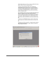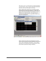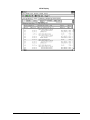
1
FuturePlus Systems Corporation
LOCAL BUS
FS2004 Users Manual
For use with Agilent Technologies Logic Analyzers
Revision 1.8
Copyright 2004 FuturePlus Systems Corporation
FuturePlus is a registered trademark of FuturePlus Systems Corporation
HOW TO REACH US
5
PRODUCT WARRANTY
6
Limitation of warranty
Exclusive Remedies
6
6
Assistance
6
INTRODUCTION
7
How to Use This Manual
7
ANALYZING THE PC CARD CARDBUS LOCAL BUS
8
Duplicating the 167xx Logic Analyzer Master Diskette
8
Accessories Supplied
8
Minimum Equipment Required
8
Signal Naming Conventions
8
Connecting the Jumpers
The Master L Clock - JP1
Current Measurements
JP1A and JP2A
9
9
9
9
Power Indicators
9
Current Protection Device
9
Swap Switches
9
SW1 and SW2
9
Test points
10
Connecting the logic analyzer to the FS2004
10
User Pins
11
How to install a PC Card Cardbus add-in card into the FS2004
11
Operation of the PC Card Cardbus add-in card
12
Series Termination Area
12
Setting up the 166x, 167x portables or the 16500 Logic Analysis System
14
Setting up the 167xx Logic Analysis System
14
Setting up the 1680/90/900 Analyzer
14
2
1680/90/900 Licensing
15
Loading 1680/90/900 configuration files and the General Purpose Probe feature
15
Configuration Files
16
Offline Analysis
16
The Format Menu
The STAT variable
The ADDR, ADDR_B and DATA variables
Using the 16517A/518A High Speed Timing Card
The CYCLE variable
19
20
21
21
21
Installation Quick Reference
24
Acquiring Data
25
The State Display
16500 Display
16700 Display
1680/90/900 Display
26
26
27
28
Error Messages
ERROR-NO DEVICE SELECTED
ERROR DEVSEL ASSERTED
SYSTEM ERROR
XXX input label could not be attached to.
XXX: input label invalid Min/Max parameters.
XXX: Failed to unattach from label
XXX: symbol could not created.
XXX: Could not save Label
XXX: Could not load Label
29
29
29
29
29
29
29
29
29
30
PC Mapper
32
Setting up the Analyzer from the diskette
32
Setting up the 1680/90/900 for PC Mapper
33
Acquiring Data
33
The State Display with the PC Card Cardbus PC Mapper
33
Error Messages
The error messages reported by the PC Card Cardbus PC Mapper are the same as those reported
with the standard non mapper version of the PC Card Cardbus Inverse Assembler.
36
PC Card Cardbus PC Mapping for memory transactions
36
Interrupt Vector Table
37
PC Card Cardbus PC Mapping - I/O Transactions
40
TIMING ANALYSIS
36
43
Installation Quick Reference
43
3
Acquiring Data
43
The Waveform Display
44
Timing Analysis using the 16517A/518A High speed timing card
44
GENERAL INFORMATION
45
Characteristics
Preprocessor Interface Compatibility
Card Edge Extender Connector
Standards Supported
Power Requirements
Logic Analyzer Required
Number of Probes Used
Minimum Clock Period (State)
Signal loading
Operations
Environmental Temperature
Altitude
Humidity
Testing and Troubleshooting
Servicing
45
45
45
45
45
45
45
45
45
45
46
46
46
46
46
Signal Connections
Test Point pinout
The Preprocessor interface pinout
Logic Analyzer Interface module
47
47
47
51
FS2004 Mechanical drawings
Logic Analyzer Interface module
Probe/Extender module
52
52
53
4
How to reach us
For Technical Support:
FuturePlus Systems Corporation
36 Olde English Road
Bedford NH 03110
TEL: 603-471-2734
FAX: 603-471-2738
On the web http://www.futureplus.com
For Sales and Marketing Support:
FuturePlus Systems Corporation
TEL: 719-278-3540
FAX: 719-278-9586
On the web http://www.futureplus.com
FuturePlus Systems has technical sales representatives in several major
countries. For an up to date listing please see
http://www.futureplus.com/contact.html.
Agilent Technologies is also an authorized reseller of many FuturePlus
products. Contact any Agilent Technologies sales office for details.
5
Product Warranty
This FuturePlus Systems product has a warranty against defects in material and
workmanship for a period of 1 year from the date of shipment. During the warranty
period, FuturePlus Systems will, at its option, either replace or repair products proven to
be defective. For warranty service or repair, this product must be returned to the factory.
For products returned to FuturePlus Systems for warranty service, the Buyer shall
prepay shipping charges to FuturePlus Systems and FuturePlus Systems shall pay
shipping charges to return the product to the Buyer. However, the Buyer shall pay all
shipping charges, duties, and taxes for products returned to FuturePlus Systems from
another country.
FuturePlus Systems warrants that its software and hardware designated by FuturePlus
Systems for use with an instrument will execute its programming instructions when
properly installed on that instrument. FuturePlus Systems does not
warrant that the operation of the hardware or software will be
uninterrupted or error-free.
Limitation of
warranty
The foregoing warranty shall not apply to defects resulting from
improper or inadequate maintenance by the Buyer, Buyer-supplied
software or interfacing, unauthorized modification or misuse,
operation outside of the environmental specifications for the product,
or improper site preparation or maintenance. NO OTHER WARRANTY IS EXPRESSED
OR IMPLIED. FUTUREPLUS SYSTEMS SPECIFICALLY DISCLAIMS THE IMPLIED
WARRANTIES OF MERCHANTABILITY AND FITNESS FOR A PARTICULAR
PURPOSE.
Exclusive Remedies
THE REMEDIES PROVIDED HEREIN ARE BUYER’S SOLE AND
EXCLUSIVE REMEDIES. FUTUREPLUS SYSTEMS SHALL NOT
BE LIABLE FOR ANY DIRECT, INDIRECT, SPECIAL, INCIDENTAL,
OR CONSEQUENTIAL DAMAGES, WHETHER BASED ON
CONTRACT, TORT, OR ANY OTHER LEGAL THEORY.
Assistance
Product maintenance agreements and other customer assistance
agreements are available for FuturePlus Systems products. For
assistance, contact the factory.
6
Introduction
The FS2004 PC Card Cardbus preprocessor and extender card performs three
functions.
•
The first is to act as an extender card, extending the card under test out of the PC
for probing
•
The second is to provide test points for the PC Card Cardbus signals to measure
the power and signal fidelity.
•
The third is to provide a complete interface between any PC Card Cardbus add-in
slot and Logic Analyzers. The preprocessor interface connects the signals from the
PC Card Cardbus to the logic analyzer inputs.
The preprocessor interface is a passive bus monitor which does not assert any signals
on the PC Card Cardbus bus. The PC Card Cardbus bus signals are terminated with
90k ohm/10pf terminators so that they are matched to the logic analyzer. Since the
preprocessor interface does not actively buffer the PC Card Cardbus signals no skew is
introduced.
The configuration software on the diskette sets up the format specification menu of the
logic analyzer for compatibility with your PC Card Cardbus target. When the state
configuration file is loaded, an inverse assembler is also loaded
which decodes PC Card Cardbus transactions into easy to read
mnemonics.
How to Use This
Manual
This manual is organized to help you quickly find the information you
need.
• Analyzing the PC Card Cardbus chapter introduces you to the
FS2004 and lists the minimum equipment required and accessories supplied for PC
Card Cardbus bus analysis.
•
The State Analysis chapter explains how to configure the FS2004 to perform state
analysis on your PC Card Cardbus target
•
The Timing Analysis chapter explains how to configure the FS2004 to perform
timing analysis on your PC Card Cardbus target
•
The General Information chapter provides information on the operating
characteristics, the test point and cable header pinout and the mechanical drawing
for the FS2004 module.
7
Analyzing the PC Card
Cardbus Local Bus
This chapter introduces you to the FS2004 and lists the
minimum equipment required and accessories supplied for PC
Card Cardbus Local Bus analysis. This chapter also contains
information that is common to both state and timing analysis.
Duplicating the 167xx
Logic Analyzer
Master Diskette
Before you use the FS2004 software on the 167xx logic
Analyzer, make a duplicate copy of the master diskette. Then
store the master diskette and use the back-up copy to configure
your logic analyzer. This will help prevent the possibility of
losing or destroying the original files in the event the diskette
wears out, is damaged, or a file is accidentally deleted.
To make a duplicate copy, use the Duplicate Diskette operation
in the disk menu of your logic analyzer. For more information,
refer to the reference manual for your logic analyzer.
Accessories
Supplied
Minimum Equipment
Required
Signal Naming
Conventions
The FS2004 product consists of the following accessories:
•
The FS2004 hardware, which includes
•
The probe/extender module and two jumpers
•
The logic analyzer interface module and one jumper
•
The inverse assembly and configuration software on a 3.5
inch diskette.
•
This operating manual
The minimum equipment required for analysis of a PC Card
Cardbus target consists of the following equipment:
•
An 165x, 1660/61/62, 1655x, 167xA, 16510A/B or 1680/90
Logic Analyzer (4 pods required)
•
The FS2004 Product
•
A PC Card Cardbus target
This operating manual uses the same signal notation as the PCI
LOCAL BUS SPECIFICATION - REVISION 2.1. That is, a #
symbol at the end of a signal name indicates that the signal’s
active state occurs when it is at a low voltage. The absence of a
# symbol indicates that the signal is active at a high voltage.
8
Connecting the
Jumpers
The Master L Clock JP1
Current Measurements
JP1A and JP2A
There are three jumpers to be configured on the FS2004.
•
JP1 on the logic analyzer interface module
•
JP1A and JP2A on the Probe/Extender module
For 166x, 1655x, 167x and 1680/90 logic analyzers the jumper
must be connected between pins 1 and 2 of JP1 on the logic
analyzer interface module. For 1650 and 16510 logic analyzers
the jumper must be connected between pins 1 and 2 of JP1 for
State analysis and pins 2 and 3 for Timing analysis.
Logic Analyzer
State/Timing
JP1
166x, 1655x, 167x and
1680/90/900
State and Timing
Connect
pins 1 and 2
1650 , 16510 and
16540/541
State analysis
Connect
pins 1 and 2
1650 , 16510 and
16540/541
Timing analysis
Connect
pins 2 and 3
The Vcc power bus may be isolated from the PC Card Cardbus
socket through two jumper blocks. Both jumpers must be
removed to isolate the power. A current meter can be inserted
to measure a card’s current consumption.
Caution: Care must be taken to insure that the current
measuring device is inserted before turning on power to the
host socket. Improper power sequencing may cause a
damaging latchup condition.
Power Indicators
Two LED power indicators display the status of the socket’s Vcc.
The PWR LED indicates that power is applied to the board.
When both the PWR LED and the 5V LED are lit, a Vcc of
greater than approximately 3.5V is present. When only the PWR
LED is lit, the Vcc is at a level of less than 3.5V.
Note: The power LEDs are designed to indicate the presence
of power on the Vcc supply pins. The LEDs do not provide an
accurate measurement of Vcc. Use a voltmeter to determine
the actual operating voltage.
Current Protection
Device
Swap Switches
SW1 and SW2
A resettable fuse protects the host from excessive current
consumption from the card. Located at V1, a Raychem
PolySwitch resettable fuse provides low resistance operation up
to 900mA.
The PC Card Cardbus Preprocessor includes two swap switches
SW1 and SW2. These switches can be used to momentarily
interrupt the CCD1# and CCD2# card detect signals and
9
simulate a card removal/insertion cycle. The switches are
located on both sides of the termination area To test the
operation of the swap switches, be sure that your PC Card
Software drivers are loaded. Momentarily press both swap
switches simultaneously. Most software drivers will issue a
removal beep followed by an insertion beep. The host socket
controller may remove power when it detects that card detects
have been removed.
Test points
All 68-pins of the interface are available to probe through clearly
marked headers. In addition, two ground posts can be used to
ground scope or high speed timing probes.
Vcc
Gnd
Gnd
C3
C7
SW1
GND
RFU
AD27
AD25
AD23
AD21
AD18
IRDY#
Vpp1
INT#
PERR#
CBE1#
AD12
AD9
AD7
AD3
AD0
CD2#
AD30
STSCH
CBE3#
SERR#
VS2
AD17
TRDY#
Vcc
STOP#
RFU
AD15
VS1
AD8
AD6
AD2
GND
GND
AD31
AD28
AUDIO
REQ#
RST#
AD19
FRAME#
VPP2
DEVSEL#
BLOCK#
AD16
AD13
AD10
RFU
AD4
-CD1
R1
R2
R3
R5
R7
R9
R12
R15
R10
R13
R16
R20
R24
R28
R32
R36
R18
R22
R26
R30
R34
R38
R42
R40
R44
R47
R50
R53
R56
R58
V1
C4
CLKRUN#
AD29
AD26
AD24
AD22
AD20
CBE2#
CLK
Vcc
GNT#
PAR
AD14
AD11
CBE0#
AD5
AD1
GND
J2
C5
J1
JP1
J2A
JP2
SW2
D2
C6
5V
Connecting the logic
analyzer to the
FS2004
PWR
C8
Gnd
The following explains how to connect the logic analyzer to the
FS2004 for either state or timing analysis:
1. Remove the probe tip assemblies from the logic
analyzer cables.
2. Plug the logic analyzer cables into the FS2004 cable
headers as shown in the appropriate table.
10
For 16540/541 Logic Analyzers
Logic Analyzer
FS2004
Comment
16540 Pod 1
Header 3
J clock
16541 Pod 1
Header 1
16541 Pod 2
Header 2
16541 Pod 3
Header 4
All Other Logic Analyzers Except The 16540/541
Logic Analyzer
User Pins
How to install a PC
Card Cardbus add-in
card into the FS2004
FS2004
POD 1
Header 1
POD 2
Header 2
POD 3
Header 3
POD 4
Header 4
Comment
L Clock (C3 on
1680/90)
FS2004 Header 4,2 and 1 each contains user defined pins.
These pins are available to the user to connect whatever
additional signals the users wishes to view along with the PC
Card Cardbus signals. These pins are located on the logic
analyzer interface module and clearly marked. The FS2004
configuration software will configure the user pins to appear as
follows:
•
User1-User4 on POD 4 channels 12 thru 15.
•
User5 on POD 1 channel 16.
•
User6 on POD 2 channel 16.
Using the PC Card Cardbus Preprocessor is relatively
straightforward. The extender card is inserted into the desired
slot in the host system. Then the PC Card Cardbus card under
test is inserted into the card connector. Simply align the PC
Card under test with the connector and gently push the module
in until it is seated in the connector.
11
Caution: Insertion and removal of the extender and PC card
should be done with care. The PC Card's fragile connectors
may be broken or bent if improper force is used. Both card
and extender should be inserted straight without any lateral
movement or force. Proper care and use of the extender card
will insure years of trouble free operation.
Operation of the PC
Card Cardbus add-in
card
The nature of an extender card is that it extends the etch length
of the bus. Due to the sensitivity of some PC Card Cardbus
designs, extending the etch length can interfere with the PC
Card Cardbus add-in card operation. Operation of the PC Card
Cardbus add-in card when installed in the card edge extender
connector is not guaranteed.
If poor signal fidelity is causing a problem with the add-in card
operation series terminating resistors can be installed on the
extender/probe card in locations R1-R62.
Series Termination
Area
A series termination area located between the test points and
the card connector allows access to all PC Card Cardbus
signals. A series of surface mount pads allows the user to add
series resistors to any signal. The SMT pads are arranged as
follows:
When shipped from the factory, the resistor pads are shorted
with PCB traces. In order to insert series resistor, these traces
must be cut prior to soldering the resistor to the board. Figure
2.4-1 and 2.4-2 illustrate the termination areas located on both
sides of the PCCextend board. Use this guide when making
modifications to the board, since the silk-screen designations
may be difficult to read.
12
SW1
CLKRUN# R1
R10
CD2#
AD29 R2
R13
AD30
AD26 R3
R16
STSCHG
AD24 R5
R20
CBE3#
AD22 R7
R24
SERR#
AD20 R9
R28
VS2
CBE2# R12
R32
AD17
GNT# R15
R36
TRDY#
INT# R18
R40
STOP#
R22
R44
RFU
AD14 R26
R47
AD15
AD11 R30
R50
VS1
CBE0# R34
R53
AD8
AD5 R38
R56
AD6
AD1 R42
R58
AD2
PAR
SW2
Figure 2.4-1 Termination Area - Component Side
AD31 R19
R4
RFU
AD28 R23
R6
AD27
AUDIO R27
R8
AD25
REQ#
R31
R11
AD23
RST# R35
R14
AD21
AD19 R39
R17
AD18
FRAME# R43
R21
IRDY#
VPP2 R46
R25
CLK
DEVSEL# R49
R29
VPP1
BLOCK# R52
R33
PERR#
AD16 R55
R37
CBE1#
AD13 R57
R41
AD12
AD10 R59
R45
AD9
RFU
R48
AD7
R60
AD4 R61
R51
AD3
CD1# R62
R54
AD0
Figure 2.4-2 Termination Area - Solder Side
13
Setting up the 166x,
167x portables or the
16500 Logic Analysis
System
The logic analyzer can be configured for PC Card Cardbus
analysis by loading the PC Card Cardbus configuration file.
Loading this file will load the PC Card Cardbus inverse
assembler and configure your logic analyzer. To load the
configuration and inverse assembler:
1. Install the FS2004 software flexible diskette in the disk
drive of the logic analyzer.
2. Configure the menu to “Load” the analyzer with the
appropriate configuration file (see table below).
Logic Analyzer
File name for State
Analysis
File name for
Timing
Analysis
16555, 167x
CBUS_555
CBUS_555
166x
CBUS_660
CBUS_660
16550
CBUS_550
CBUS_550
1650 and
16510
CBUS_510S
CBUS_510T
3. Execute the load operation to load the file into the logic
analyzer.
For 1655x, 167x, 16540/541 and 166x REV2.0 (system software
or later) users an enhanced inverse assembler is included on the
preprocessor software diskette. After loading the above file, load
the file IAPCIEXE. This will configure the STATE listing menu to
include INVASM OPTIONS.
Please note that 166x and 1655x, 167x users do not need to
reload any files from the diskette when switching between
state and timing analysis.
Setting up the 167xx
Logic Analysis System
The 16600/16700 requires a special install procedure to install
the PCI software. To accomplish this, insert the diskette labeled
16700/16702 PCI Analysis Probe Install disk for the FS2004
into the 16600/700 diskette drive. From the SYSTEM
ADMINISTRATION TOOLS select INSTALL under SOFTWARE.
From the SOFTWARE INSTALL screen select the FLEXIBLE
DISK and APPLY. Once the title appears, select it and then
select INSTALL. This procedure does not need to be
repeated. It only needs to be done the first time the PCI
Analysis Probe is used.
When the install is complete, load the appropriate configuration
file from /logic/configs/FuturePlus/FS2004 directory.
Setting up the
1680/90/900 Analyzer
The 1680/90/900 Analyzer is a PC based application that
requires a PC running the Windows OS or a 16900 frame.
Before installing the protocol decoder for the PCI protocol on a
PC you must install the Agilent logic analyzer software. Once
the Agilent logic analyzer software is installed, you can install the
14
FS2004 protocol decoder by placing the CD-ROM disk into the
CD-ROM drive of the target computer or Analyzer and executing
the .exe setup program that is contained on the disk. The .exe
setup file can be executed from within the File Explorer PC
Utility. You must navigate to the .exe file on the CD-ROM disk
and then double click the .exe file name from within the File
Explorer navigation panel.
The installation procedure does not need to be repeated. It
only needs to be done the first time the Analysis Probe
Adapter is used.
1680/90/900
Licensing
Loading 1680/90/900
configuration files
and the General
Purpose Probe
feature
The PCI Inverse Assembler is a licensed product that is locked
to a single hard drive. The licensing process is performed by
Agilent. There are instructions on this process on the SW
Entitlement certificate provided with this product.
When the software has been licensed you should be ready to
load a configuration file. You can access the configuration files
by clicking on the folder that was placed on the desktop. When
you click on the folder it should open up to display all the
configuration files to choose from. If you put your mouse cursor
on the name of the file a description will appear telling you what
the setup consists of, once you choose the configuration file that
is appropriate for your configuration the 16900 operating system
should execute. The protocol decoder automatically loads when
the configuration file is loaded. If the decoder does not load, you
may load it by selecting tools from the menu bar at the top of the
screen and select the decoder from the list.
Once you have loaded a configuration file on the 169xx machine
you can find out how to attach the logic analyzer cables to the
probe by going to the workspace and selecting Properties on the
General Purpose Probe tool icon that appears before the logic
analyzer icon. Once you click on the Properties box a new
window will appear showing which analyzer pod attaches to
which probe cable.
The figure below may differ from your display; this is an example
of how the display looks in general.
15
Refer to the table below for a list of analyzers and corresponding
configuration files.
Configuration Files
167xx Analyzer
169xx Analyzer
16550
CP204_1
16555
CP204_2
16717/8/9, 16750/1/2
CP204_3
1680/90, 16750/1/2,
1691x
Offline Analysis
State/Timing
CP204_4.xml
Data that is saved on a 167xx analyzer in fast binary format, or
16900 analyzer data saved as a *.ala file, can be imported into
the 1680/90/900 environment for analysis. You can do offline
analysis on a PC if you have the 1680/90/900 operating system
installed on the PC, if you need this software please contact
Agilent.
Offline analysis allows a user to be able to analyze a trace offline
at a PC so it frees up the analyzer for another person to use the
analyzer to capture data.
If you have already used the license that was included with your
package on a 1680/90/900 analyzer and would like to have the
16
offline analysis feature on a PC you may buy additional licenses,
please contact FuturePlus sales department.
In order to view decoded data offline, after installing the
1680/90/900 operating system on a PC, you must install the
FuturePlus software. Please follow the installation instructions
for “Setting up 1680/90/900 analyzer”. Once the FuturePlus
software has been installed and licensed follow these steps to
import the data and view it.
From the desktop, double click on the Agilent logic analyzer icon.
When the application comes up there will be a series of
questions, answer the first question asking which startup option
to use, select Continue Offline. On the analyzer type question,
select cancel. When the application comes all the way up you
should have a blank screen with a menu bar and tool bar at the
top.
For data from a 1680/90/900 analyzer, open the .ala file using
the File, Open menu selections and browse to the desired .ala
file.
For data from a 16700, choose File -> Import from the menu bar,
after selecting import select “yes” when it asks if the system is
ready to import 16700 data.
17
After clicking “next” you must browse for the fast binary data file
you want to import. Once you have located the file and clicked
start import, the data should appear in the listing.
After the data has been imported you must load the protocol
decoder before you will see any decoding. To load the decoder
select Tools from the menu bar, when the drop down menu
appears select Inverse Assembler, then choose the name of the
decoder for your particular product. The figure below is a
general picture; please choose the appropriate decoder for the
trace you are working with.
After the decoder has loaded, select Preferences if required,
from the overview screen and set the preferences to their correct
value in order to decode the trace properly. This is a general
requirement, some decoders do not have preferences, if this is
the case then no preference setting is necessary.
18
The Format Menu
The FS2004 diskette sets up the format menu as shown in the
following table (1655x, 167x,16510 and 166x, 1680/90). This
format is the same for both Timing and State Analysis.
Label
Clk
Inputs
STAT
Pod 4
Pod 3
9-0
14-0
ADDR
Pod 2
Pod 1
15-0
15-0
16
16
ADDR_B
USER2_1
INTD_A
14-11
RESET
10
C/B3_0
9-6
15-0
DATA
DEVSEL
5
STOP
4
LOCK
3
PERR
2
SERR
1
PAR
0
SD/SB0
5-6
ACK/RQ
1-0
IRDY
7
19
Label
Clk
Inputs
FRAME
8
TRDY
9
PC Card
Cardbus
CLK
The STAT variable
Pod 4
Pod 3
Pod 2
Pod 1
L
IDSEL
2
GNT
3
REQ
4
CYCLE
9-7
9-4
The STAT variable is used by the PC Card Cardbus inverse
assembler to decode PC Card Cardbus bus transactions. It
should not be changed or deleted from the format menu. The
signals that make up the STAT variable are listed in the following
table. The STAT variable can be useful to set up SYMBOLS
since it contains all of the key PC Card Cardbus control and
status signals.
STAT Variable
PC Card Cardbus Bus
Signal Name
Bit 24
TRDY#
Bit 23
FRAME#
Bit 22
IRDY#
Bit 21
SDONE
Bit 20
SB0#
Bit 19
REQ#
Bit 18
GNT#
Bit 17
IDSEL
Bit 16
ACK64#
Bit 15
REQ64#
Bit 14
INTD#
Bit 13
INTC#
Bit 12
INTB#
Bit 11
INTA#
20
STAT Variable
PC Card Cardbus Bus
Signal Name
Bit 10
RESET#
Bit 9
C/BE3#
Bit 8
C/BE2#
Bit 7
C/BE1#
Bit 6
C/BE0#
Bit 5
DEVSE#L
Bit 4
STOP#
Bit 3
LOCK#
Bit 2
PERR#
Bit 1
SERR#
Bit 0
PAR
The ADDR, ADDR_B and
DATA variables
The ADDR variable is AD[31-0] bits of the PC Card Cardbus
bus. The DATA variable is a dummy variable that needs to be
defined for the PC Card Cardbus inverse assembler. These
variables should not be changed or deleted from the format
Menu.
Using the 16517A/518A
High Speed Timing Card
The logic analyzer interface card can be removed for easy
access to test points. These test points can be used to attach
the flying lead set of the 16517A/518A high speed timing card.
The PC Card Cardbus Preprocessor diskette has a configuration
file named FS18PE that can be used as a starting point. Use this
file and the stake pinout shown in the General Information
chapter to connect the 16517A/518A to the FS2004 stake pins.
The CYCLE variable
The CYCLE variable is made up of the following PC Card
Cardbus signals: TRDY#, FRAME#, IRDY#, C/BE(3,0),
DEVSEL# and STOP#. This variable has 30 symbols defined
that can be used to help make triggering, timing analysis and
pattern filtering easier. The following lists the bit pattern and the
corresponding symbol.
21
Symbol
TRDY# FRAME# IRDY# C/BE(3:0) DEVSEL# STOP#
INTACK
1
0
1
0000
1
1
SPEC_CYC
1
0
1
0001
1
1
I/O_RD
1
0
1
0010
1
1
I/O_WR
1
0
1
0011
1
1
RESVRD
1
0
1
0100
1
1
RESVRD
1
0
1
0101
1
1
MEM_RD
1
0
1
0110
1
1
MEM_WR
1
0
1
0111
1
1
RESRVD
1
0
1
1000
1
1
RESRVD
1
0
1
1001
1
1
CON_RD
1
0
1
1010
1
1
CON_WR
1
0
1
1011
1
1
MEMRDM
1
0
1
1100
1
1
DAD_CY
1
0
1
1101
1
1
MEMRDL
1
0
1
1110
1
1
MEMWRI
1
0
1
1111
1
1
IO_XACTION
1
0
1
001X
1
1
MEM_XACTION
1
0
1
011X
1
1
CONFIG_XACTION
1
0
1
101X
1
1
ADD_CYCLE
1
0
1
XXXX
1
1
DATA_XFER
0
0
0
XXXX
0
1
WAIT_TARGET
1
X
0
XXXX
0
1
WAIT_INITIATOR
0
X
1
XXXX
0
1
DATA_FINALXFER
0
1
0
XXXX
0
1
STOP_NOXFER
X
0
1
XXXX
0
0
STOP_DATAXFER
0
X
0
XXXX
0
0
STOP_RETRY
1
1
0
XXXX
0
0
TARGET_ABORT
1
0
1
XXXX
1
0
22
Symbol
TRDY# FRAME# IRDY# C/BE(3:0) DEVSEL# STOP#
IDLE
X
1
1
XXXX
X
X
WAIT_NODEVSEL
X
X
0
XXXX
1
1
WAIT_NODEVSEL/F_O
X
0
0
XXXX
1
1
23
State Analysis
This chapter explains how to configure the FS2004 to perform
state analysis on your PC Card Cardbus target system. The
configuration software sets up the format specification menu of
the logic analyzer for compatibility with your PC Card Cardbus
target system. The next chapter explains how to configure the
FS2004 to perform timing analysis.
The FS2004 preprocessor interface does not require that a PC
Card Cardbus add-in card be installed in the FS2004 card edge
extender connector.
Installation Quick
Reference
The following procedure describes the major steps required to
perform state measurements with the FS2004 module.
1. Set the jumpers to the appropriate position on the
FS2004 module. See page 9 of this manual for details.
2. After removing the probe tip assemblies, plug the logic
analyzer cables into the preprocessor interface cable
headers. See page 11 of this manual for details.
3. Install the FS2004 module into a slot in the target PC
Card Cardbus Local bus.
4. Load the logic analyzer configuration file by loading the
appropriate file. See page 14 of this manual for details.
24
Acquiring Data
Touch RUN and, as soon as there is activity on the bus, the logic
analyzer will begin to acquire data. The analyzer will continue to
acquire data and will display the data when the analyzer memory
is full, the trigger specification is TRUE or when you touch
STOP.
The logic analyzer will flash “Slow or Missing Clock” if it does not
see the PC Card Cardbus signal CLK toggling.
To capture PCI data, click the green arrow (run) button that is
located on the tool bar at the top of the screen.
Capture Data Figure on 1680/90/900
25
The State Display
Captured data is as shown in the following figure. The below
figure displays the state listing after disassembly. The inverse
assembler is constructed so the mnemonic output closely
resembles the actual commands, status conditions, messages
and phases specified in the PCI Local Bus specification.
Symbols have also been defined to help aid in analysis. The
non-disassembled state listing displays PC Card Cardbus bus
mnemonics in addition to data. All data is displayed in hex. One
exception is the decode of the address for a CONFIGURATION
READ or a CONFIGURATION WRITE transaction. The
Function (FUNC=) and Bus (BUS=) data is displayed in decimal.
16500 Display
26
16700 Display
27
1680/90/900 Display
28
Error Messages
The following error messages are reported by the PC Card
Cardbus inverse assembler.
ERROR-NO DEVICE SELECTED
This error is displayed during a non special cycle data phase
when IRDY and TRDY are asserted and DEVSEL is not
asserted.
ERROR DEVSEL ASSERTED
This error is displayed during a special cycle data phase if
DEVSEL is asserted.
SYSTEM ERROR
This error is displayed anytime SERR# is asserted.
1680/90/900 Errors:
XXX input label could not be attached to.
This error is displayed when the 1680/90 IA is being
started and a failure occurs during the creation of an input
label/column.
XXX: input label invalid Min/Max parameters.
This error is displayed during the creation of a
label/column. The IA expects the label/column to fall
within a min/max number of bits which has been violated.
XXX: Failed to unattach from label
This error is displayed when the 1680/90 IA is being exited
and a failure occurs during the label/column destruction
XXX: output label could not be created.
This error is displayed when the 1680/90 IA is being
started and a failure occurs when an output label/column
is being constructed
XXX: symbol could not created.
This error is displayed when the 1680/90 IA is being
started and a failure occurs when an output or input
label/column symbol could not be created
XXX: Could not save Label
29
This error is displayed when the 1680/90 IA configuration file is
being created and/or updated. The configuration data for the
specified label could not be written to the file and thus will be
lost.
XXX: Could not load Label
This error is displayed when the 1680/90 IA configuration
file is being read. The configuration data for the specified
label could not be read to the file and thus will be lost.
INVASM OPTIONS
INVASM OPTIONS is available with the following logic
analyzers.
•
16505A
•
1655x, 167xA in a 16500B main frame
•
16540/541 in a 16500B main frame
•
166x series with 2.0 system software
•
167xx series
1680/90 does not implement an INVASM Options menu
INVASM OPTIONS for the 165xxcan be invoked by selecting
INVASM OPTIONS from the state listing display. The following
selection will be displayed.
INVASM OPTIONS for the 16700 family can be invoked by
selecting INVASM from the state listing display and choose filter
to display the color options. Below is a display taken from the
16700 showing the filter options screen. To filter out any state
just point to the state you want filtered out, and click on it. To
turn back on simply click on the state again.
30
16700 Invasm Filter Options
Filtering
The acquired state listing display can be modified to filter out any
combination of the above transactions or cycles by selecting the
show/suppress button to the right of the transaction list.
For 16700 users, select filter under INVASM in the state listing.
For 1680/90 users, select the Filter/Colorization pull down
menus in the state listing and create a filter (downstream) tool.
The 1680/90 IA allows filtering just like the 16700/702
environments. You may filter on any label, when using the filter
tags label you can select symbols to make choosing transactions
easier. To create a filter, choose Tools->New->Filter/Colorize.
Then fill in the information on the window that opens up. You
must create a new filter for each item you want filtered. To
remove filters that you no longer want, go to Tools->Overview
and then choose the filter you want removed and click Delete.
31
PC Mapper
The PC Card Cardbus Preprocessor PC Mapper software is an
enhanced version of the PC Card Cardbus Preprocessor inverse
assembler and is for use only with PC Card Cardbus
Preprocessor from FuturePlus Systems Corporation.
The
enhancement includes PC Card Cardbus I/O and memory
address decode to indicate common PC access.
Setting up the
Analyzer from the
diskette
After the configuration file is loaded the PC Card Cardbus PC
Mapper software can be loaded:
1. Install the PC Card Cardbus Preprocessor software
flexible diskette in the disk drive of the logic analyzer.
2. Configure the menu to “Load” the analyzer with the
appropriate file (see table).
Logic Analyzer
File name
16500B mainframe with 16555,
16550, 167x, or 16540/541 logic
analyzer
IAPCIMXE
16500B mainframe with 16510
IAPCIMX
16500A mainframe (all logic
analyzer models)
IAPCIMX
166x series (with REV 2.2 system
software)
IAPCIMXE
165x logic analyzers
IAPCIMX
3. Execute the load operation to load the file into the logic
analyzer.
IFS2004E is the inverse assembler for all logic analyzers
installed into the 16600/700 and is auto loaded when the
configuration file is loaded.
To select PC Mapper function on the 16700, select INVASM
from the state listing display then select PREFERENCES it will
come up with a box and there you can choose to turn on PC
Mapper or suppress PC Mapper. The picture below displays PC
Mapper function enabled on the 16700.
32
Setting up the
1680/90/900 for PC
Mapper
Acquiring Data
PC Mapper is currently not available on the 1680/90/900.
Data can be acquired by touching the RUN button. As soon as
there is activity on the bus, the logic analyzer will begin to
acquire data. The analyzer will continue to acquire data and will
display the data when the analyzer memory is full, the trigger
specification is TRUE or when you touch STOP.
The logic analyzer will flash “Slow or Missing Clock” if the PC
Card Cardbus Clock signal is not being detected by the logic
analyzer. In this case, check the logic analyzer to PC Card
Cardbus Preprocessor connection.
The State Display
with the PC Card
Cardbus PC Mapper
Captured data is as shown in the following figure. The first figure
displays the state listing after disassembly. The PC Card
Cardbus PC Mapper is constructed so the mnemonic output
closely resembles the actual commands, status conditions,
messages and phases specified in the PC Card Cardbus Local
Bus specification. Symbols have also been defined to help aid in
analysis. The non-disassembled state listing displays PC Card
Cardbus bus mnemonics in addition to data. All data is displayed
in hex. One exception is the decode of the address for a
CONFIGURATION READ or a CONFIGURATION WRITE
transaction. The Function (FUNC=) and Bus (BUS=) data is
displayed in decimal.
33
The above display data using the PC Card Cardbus Inverse
Assembly software without the PC Card Cardbus PC Mapper
functionality is shown as follows.
The following listing shows the PC Mapper preference selected
on the 16700.
34
The following listing shows the PC Mapper preference
suppressed on the 16700
35
Error Messages
The error messages reported by the PC Card Cardbus PC
Mapper are the same as those reported with the standard non
mapper version of the PC Card Cardbus Inverse Assembler.
The acquired state listing display can be modified to filter out any
combination of the above transactions or cycles by selecting the
show/suppress button to the right of the transaction cycle list.
PC Card Cardbus PC
Mapping for memory
transactions
This section lists the addresses, the commands and
corresponding mapping done by the PC Card Cardbus
Mapper software.
For information on the standard
configuration register mapping please refer to the PCI Local
Specification Rev 2.1.
Address bits 23-0
PC Mapper output
greater than 0FFFFFH
0FFFFF-0E0000H
0DFFFF-0C0000H
0BFFFF-0A0000H
09FFFF-000400H
0003FF-000000H
System Memory
System BIOS
ROM Scan
Video Memory
System Memory
See Interrupt Vector Table
36
the
PC
PCI
Bus
Interrupt Vector
Table
Address bits
23-0
PC Mapper output
0003C4H
000200H
0001E0H
0001DCH
0001D8H
0001D4H
0001D0H
0001CCH
0001C8H
0001C4H
0001C0H
0001A0H
00019CH
000180H
00012CH
000128H
00011CH
000118H
000110H
00010CH
000108H
000104H
000100H
000080H
00007CH
000078H
000074H
000070H
00006CH
000068H
000064H
000060H
00005CH
000058H
000054H
000050H
00004CH
000048H
000044H
000040H
00003CH
000038H
000034H
000030H
00002CH
000028H
000024H
000020H
00001CH
000018H
000014H
000010H
INT #F1-FF USER PROGRAMS
INT #80-F0 BASIC
INT #78-7F USER PROGRAMS
INT #77 IRQ15
INT #76 IRQ14
INT #75 IRQ13
INT #74 IRQ12
INT #73 IRQ11
INT #72 IRQ10
INT #71 IRQ9
INT #70 IRQ8
INT #68-6F RESERVED
INT #67 EXP MEM MANG
INT #60-66 USER PROGRAMS
INT #4B-5F RESERVED
INT #4A USER RTC ALARM
INT #47-49 RESERVED
INT #46 HD DISK #1 PARAM
INT #44-45 RESERVED
INT #43 VIDEO CHAR TABLE
INT #42 EGA BIOS
INT #41 HD DISK #0 PARAM
INT #40 FLOPPY DISK ISR
INT #20-3F RESERVED DOS
INT #1F VIDEO CHAR TABLE
INT #1E FLOPPY PARAMS
INT #1D AVAILABLE
INT #1C AVAILABLE
INT #1B KEYBOARD BREAK
INT #1A RTC ISR
INT #19 BOOSTRAP LOADER
INT #18 ROM BASIC
INT #17 LPT PRINTER BIOS
INT #16 KEYBOARD BIOS
INT #15 SYS SERVICE BIOS
INT #14 SERIAL PORT BIOS
INT #13 FLOPPY DISK BIOS
INT #12 MEM SIZE INT
INT #11 EQUIP LIST
INT #10 VIDEO BIOS
INT #0F IRQ7 LPT1
INT #0E IRQ6 FLOPPY DISK
INT #0D IRQ5 LPT2
INT #0C IRQ4 SERIAL #1
INT #0B IRQ3 SERIAL #2
INT #0A IRQ2 SLAVE INT
INT #09 KEYBOARD
INT #08 IRQ0 SYS TIMER
INT #07 NUM COPROCESSOR
INT #06 INVALID OPCODE
INT #05 PRINT SCREEN
INT #04 OVERFLOW DETECT
37
00000CH
38
INT #03 BREAKPOINT TRACE
Address bits
23-0
PC Mapper output
000008H
000004H
000000H
INT #02 NMI
INT #01 SINGLE STEP
INT #00 DIVIDE BY ZERO
39
PC Card Cardbus PC
Mapping - I/O
Transactions
Address bits
23-0
PC Mapper output
0000H
0001H
0002H
0003H
0004H
0005H
0006H
0007H
0008H
0009H
000AH
000BH
000CH
000DH
000EH
000FH
0018H
001AH
0020H
0021H
0040H
0042H
0043H
0044H
0047H
0060H
0061H
0064H
0070H
0071H
0074H
0075H
0076H
0081H
0082H
0083H
0087H
0089H
008AH
008BH
008FH
0090H
0091H
0092H
0094H
0096H
00A0H
00A1H
00C0H
00C2H
00C4H
00C6H
MSTR DMA CH 0
MSTR DMA CH 0
MSTR DMA CH 1
MSTR DMA CH 1
MSTR DMA CH 2
MSTR DMA CH 2
MSTR DMA CH 3
MSTR DMA CH 3
MSTR DMA STAT REG
UNKNOWN IO DEVICE
MSTR DMA MASK REG
MSTR DMA MODE REG
MSTR DMA CLR BYTE PTR
MSTR DMA MSTR CLEAR
MSTR DMA CLEAR MASK
MSTR DMA WRT MASK
MSTR DMA CH EXT FUNCT REG
MSTR DMA EXT FUNCT
MSTR INT REQ REG
MSTR INT REQ REG2
INTERVAL TIMER TIMER 0
INTERVAL TIMER SPKR TIMER
INTRVAL TIMER #1 CNTRL
INTERVL TIMER #2 WATCHDOG
INTERVAL TIMER #2 CNTRL
KEYBOARD/MOUSE DATA PORT
SYSTEM CONTOL PORT B
KEYBOARD/MOUSE CMD PORT
RTC/CMOS RAM ADDR PORT
RTC/CMOS RAM DATA PORT
EXT CMOS RAM ADDR PORT
EXT CMOS RAM ADDR PORT
EXT CMOS RAM DATA PORT
CH 2 DMA PAGE REGISTER
CH 3 DMA PAGE REGISTER
CH 1 DMA PAGE REGISTER
CH 0 DMA PAGE REGISTER
CH 6 DMA PAGE REGISTER
CH 7 DMA PAGE REGISTER
CH 5 DMA PAGE REGISTER
CH 4 DMA PAGE REGISTER
ARB CNTRL POINT REG
FEEDBACK REG
SYSTEM CONTROL PORT A
SYS SETUP/CARD ENABLE REG
ADAPTOR SETUP/ENABLE REG
SLAVE INTERRUPT CNTRLR
SLAVE INTERRUPT CNTRLR
SLAVE DMA CH4 MEM ADDR
SLAVE DMA CH4 TRANS COUNT
SLAVE DMA CH5 MEM ADDR
SLAVE DMA CH5 TRANS COUNT
40
00C8H
SLAVE DMA CH6 MEM ADDR
Address bits
23-0
PC Mapper output
00CAH
00CCH
00CEH
00D0H
00D4H
00D6H
00D8H
00DAH
00DCH
00DEH
00E0H
00E1H
00F1H
00F8H
00F9H
00FAH
00FBH
00FCH
0100H
0101H
0102H
0103H
0104H
0105H
0106H
0107H
0278H
0279H
027AH
02F8H
02F9H
02FAH
02FBH
02FDH
02FEH
02FFH
0378H
0379H
037AH
03B4H
03B5H
03BAH
03BCH
03BDH
03BEH
03C0H
03C1H
03C2H
03C3H
03C4H
03C5H
SLV DMA CH6 TRANS COUNT
SLAVE DMA CH7 MEM ADDR
SLAVE DMA CH7 TRANS COUNT
SLV DMA STATUS REG CH 4-7
SLV DMA MASK REG CH 4-7
SLAVE DMA MODE REG CH 4-7
SLAVE DMA CLEAR BYTE PNTR
SLAVE DMA MASTER CLEAR
SLV DMA CLR MASK CH 4-7
SLAVE DMA WRITE MASK REG
IBM MODELS - ENCODE REG
IBM MODELS - ENCODE REG
NUMERIC COPROCESSOR RESET
NUMERIC COPROCESSOR PORT
NUMERIC COPROCESSOR PORT
NUMERIC COPROCESSOR PORT
NUMERIC COPROCESSOR PORT
NUMERIC COPROCESSOR PORT
ADAPTER CARD POS REG 0
ADAPTER CARD POS REG 1
SYS BD/ADP CD POS REG 2
SYS BD/ADP CD POS REG 3
ADAPTER CARD POS REG 4
ADAPTER CARD POS REG 5
ADAPTER CARD POS REG 6
ADAPTER CARD POS REG 6
PARALLEL PORT 3 DATA PORT
PARALLEL PORT 3 STAT PORT
PARALLEL PORT 3 CMD PORT
SERIAL PORT 2 XMIT/REC
SER PORT 2 DIV LATCH/INT
SERIAL PORT 2 INT ID REG
SERIAL PORT 2 CNTRL REG
SERIAL PORT 2 MODEM CNTRL
SERIAL PORT 2 MODEM STAT
SERIAL PORT 2 SCRTCH REG
PARALLEL PORT 2 DATA PORT
PARALLEL PORT 2 STAT PORT
PARALLEL PORT 2 CMD PORT
VGA CRT CNTRLR ADDR REG
VGA CRT CNTRLR DATA REG
VGA STAT 1/FEATURE CNTRL
PARALLEL PORT 1 DATA PORT
PARALLEL PORT 1 STAT PORT
PARALLEL PORT 1 CMD PORT
VGA ATTRIBUTE CNTRLR ADDR
VGA ATTRIBUTE CNTRLR DATA
VGA OUTPUT/STAT REG
VGA VIDEO SUBSYSTM ENABLE
VGA SEQUENCER ADDR REG
VGA SEQUENCER DATA REG
41
03C6H
03C7H
VIDEO DAC PEL MASK
VIDEO DAC PAL ADDR/STAT
Address bits
23-0
PC Mapper output
03C8H
03C9H
03CAH
03CCH
03CEH
03CFH
03D4H
03D5H
03DAH
03F0H
03F1H
03F2H
03F4H
03F5H
03F7H
03F8H
03F9H
03FAH
03FBH
03FCH
03FDH
03FEH
03FFH
0680H
VIDEO DAC PAL ADDR/WRITE
VIDEO DAC PALETTE DATA
VGA FEATURE CONTOL REG
VGA MISC OUTPUT REG
VGA GRAPHICS CNTRLR ADDR
VGA GRAPHICS CNTRLR ADDR
VGA CRT CNTRLR ADDR REG
VGA GRAPHICS CNTRLR DATA
VGA COLOR STAT 1/FEATURE
FLOPPY STATUS REG A
FLOPPY STATUS REG B
FLOPPY DIGITAL OUTPUT REG
FLOPPY DISK CNTRLR STAT
FLOPPY DISK CNTRLR DATA
FLOPPY CONFIG CONTROL REG
SERIAL PORT 1 XMIT/RCV BUF
SER PORT 1 DIV LATCH/INT
SERIAL PORT 1 INT ID/FIFO
SERIAL PORT 1 LINE CNTRL
SERIAL PORT 1 MODEM CNTRL
SERIAL PORT 1 STAT REG
SERIAL PORT 1 MODEM STAT
SERIAL PORT 1 SCRATCH REG
MANUFCTURNG CHCKPNT PORT
42
Timing Analysis
Since the FS2004 interface contains only passive matching
terminators it introduces negligible skew to the PC Card Cardbus
Local Bus signals.
Installation Quick
Reference
The following procedure describes the major steps required to
perform timing analysis measurements with the FS2004 module.
1. Set the jumpers to the appropriate position on the
FS2004 module. See page 9 of this manual for details.
2. After removing the probe tip assemblies, plug the logic
analyzer cables into the logic analyzer interface module
headers. See page 10 of this manual for details.
3. Install the FS2004 module into a slot in the target PC
Card Cardbus Local bus.
4. Load the logic analyzer configuration file by loading the
appropriate file from the preprocessor interface diskette.
See page 14 of this manual for details.
Acquiring Data
Touch RUN and, as soon as there is activity on the bus, the logic
analyzer will begin to acquire data. The analyzer will continue to
acquire data and will display the data when the analyzer memory
is full, the trigger specification is TRUE or when you touch
STOP.
The logic analyzer will flash “Waiting for Trigger” if the trigger
specification has not been met.
43
The Waveform
Display
Captured data is displayed as shown in the following figure.
Timing Analysis
using the
16517A/518A High
speed timing card
Removing the logic analyzer interface module will give access to
the test point area. This is a convenient way of attaching the
high speed timing card. Using the 16517A/518A high speed
timing card, measurements of 250ps can be made.
44
General Information
This chapter provides additional reference information including
the characteristics and signal connections for the FS2004
module.
Characteristics
The following operating characteristics are not specifications, but
are typical operating characteristics for the FS2004 module.
Preprocessor Interface
Compatibility
32 bit PC Card Cardbus Local bus accepting the Type 1 form
factor. All PC Card Cardbus local bus ground pins are connected
to the ground plane of the Extender/Probe card and the logic
analyzer interface module.
Card Edge Extender
Connector
Standards Supported
This connector is a Type 1 connector. All of the signals from the
PC Card Cardbus bus are routed to the extender connector.
Power Requirements
The FS2004 preprocessor draws a small amount of power from
the PC Card Cardbus target for the LED. The PC Card Cardbus
add-in card installed in the FS2004 can draw power from the +/12V, 3.3V and the 5V pins as if it were installed without the
FS2004.
Logic Analyzer Required
166x, 1661, 1662, 1655x, 167x, 16510, 1650, 16540/541,
167xx, 1680/90/900. 1675x, 1695x, 1691x.
Number of Probes Used
The PCI Local Bus Specification Revision 2.1 and PC Card ‘95
standard.
The preprocessor interface uses 4 cable headers.
Minimum Clock Period
(State)
Not limited by the preprocessor interface logic. Clocking is
specified by the logic analyzer.
Signal loading
The FS2004 Preprocessor logic presents one 10pf/90k ohm load
on each PC Card Cardbus bus signal. The card edge extender
connector adds an addition 2pf. If stake pins are installed as test
points they add 1pf. If the test points are configured with an
additional PC Card Cardbus connector this connector adds
approximately 2pf.
The etch and associated via’s add
approximately 1pf of additional capacitance.
Operations
All PC Card Cardbus operations supported by the hardware and
the inverse assembler.
45
Environmental
Temperature
Operating:0 to 55 degrees C (+32 to +131 degrees F)
Altitude
Operating: 4,6000m (15,000 ft)
Non operating:-40 to +75 degrees C (-40 to +167 degrees F)
Non operating: 15,3000m (50,000 ft)
Humidity
Testing and
Troubleshooting
Servicing
Up to 90% non condensing. Avoid sudden, extreme temperature
changes which would cause condensation on the FS2004
module.
There are no automatic performance tests or adjustments for the
FS2004 module. If a failure is suspected in the FS2004 module
contact the factory or your FuturePlus Systems authorized
distributor.
The repair strategy for the FS2004 is module replacement.
However, if parts of the FS2004 module are damaged or lost
contact the factory for a list of replacement parts.
46
Signal Connections
The FS2004 contains 4, forty pin headers for connection to
Agilent logic analyzers and test points for scope or flying lead
logic analyzer connection.
Test Point pinout
The FS2004 test points can be accessed by removing the logic
analyzer interface module and attaching directly to the test
points. The signal names are clearly marked on the etch.
The Preprocessor
interface pinout
The logic analyzer interface module attaches to the test pints on
the probe/extender card. This then attaches to the logic
analyzer thru 40 pin headers. The below figure displays how
pins of the 40 pin cable headers are numbered.
39 37 35 33 31 29 27 25 23 21 19 17 15 13 11 9 7 5 3 1
40 38 36 34 32 30 28 26 24 22 20 18 16 14 12 10 8 6 4 2
The following tables list the FS2004 cable headers and the
corresponding PC Card Cardbus signals after these signals
have been terminated by the 90K ohm/10pf terminators.
47
Preprocessor
Cable Header and
Pin number
Header 1 pin 3
48
Logic Analyzer
channel number
CLK/16
PC Card Cardbus
Signal name
USER5
5
no connect
7
15
AD15
9
14
AD14
11
13
AD13
13
12
AD12
15
11
AD11
17
10
AD10
19
9
AD09
21
8
AD08
23
7
AD07
25
6
AD06
27
5
AD05
29
4
AD04
31
3
AD03
33
2
AD02
35
1
AD01
37
0
AD00
Preprocessor
Cable Header and
Pin number
Header 2 pin 3
49
Logic Analyzer
channel number
CLK/16
PC Card Cardbus
Signal name
USER6
5
no connect
7
15
AD31
9
14
AD30
11
13
AD29
13
12
AD28
15
11
AD27
17
10
AD26
19
9
AD25
21
8
AD24
23
7
AD23
25
6
AD22
27
5
AD21
29
4
AD20
31
3
AD19
33
2
AD18
35
1
AD17
37
0
AD16
Preprocessor
Cable Header and
Pin number
Header 3 pin 3
50
Logic Analyzer
channel number
CLK/16
PC Card Cardbus
Signal name
PCI Clock here
for 166x/550
and 16510
State analysis.
5
no connect
7
15
PCI
Clock
16510 Timing
analysis only.
9
14
CCLKRUN#
11
13
CCD2#
13
12
CCD1#
15
11
CINT#
17
10
RST#
19
9
C/BE3#
21
8
C/BE2#
23
7
C/BE1#
25
6
C/BE0#
27
5
DEVSEL#
29
4
STOP#
31
3
LOCK#
33
2
PERR#
35
1
SERR#
37
0
PAR
Preprocessor
Cable Header and
Pin number
Logic Analyzer Interface
module
Header 4 pin 3
51
Logic Analyzer
channel number
PC Card Cardbus
Signal name
CLK/16
5
no connect
7
15
USER4
9
14
USER3
11
13
USER2
13
12
USER1
15
11
VS2
17
10
VS1
19
9
TRDY#
21
8
FRAME#
23
7
IRDY#
25
6
CSTSCHG
27
5
CAUDIO
29
4
REQ#
31
3
GNT#
33
2
RFU3
35
1
RFU2
37
0
RFU1
FS2004 Mechanical
drawings
Logic Analyzer Interface
module
52
CARDBUS
53
CLKRUN#
AD29
AD26
AD24
AD22
AD20
CBE2#
CLK
Vcc
GNT#
PAR
AD14
AD11
CBE0#
AD5
AD1
GND
J1
GND
RFU
AD27
AD25
AD23
AD21
AD18
IRDY#
Vpp1
INT#
PERR#
CBE1#
AD12
AD9
AD7
AD3
AD0
CD2#
AD30
STSCH
CBE3#
SERR#
VS2
AD17
TRDY#
Vcc
STOP#
RFU
AD15
VS1
AD8
AD6
AD2
GND
J2
GND
AD31
AD28
AUDIO
REQ#
RST#
AD19
FRAME#
VPP2
DEVSEL#
BLOCK#
AD16
AD13
AD10
RFU
AD4
-CD1
PCCextend
D2
5V
R40
R44
R47
R50
R53
R56
R58
R18
R22
R26
R30
R34
R38
R42
SW2
R10
R13
R16
R20
R24
R28
R32
R36
R1
R2
R3
R5
R7
R9
R12
R15
SW1
PWR
Gnd
C3
C4
C6
C5
Vcc
JP2
JP1
V1
C8
C7
Gnd
Gnd
J2A
Probe/Extender module