1
...•..~
.. :,.,..' ...
~ ~
.I
REFERENCE MANUAL
SHUGART
706/712
HARD DISK
Silicon Valley Computer
.'. ( 4 0 8 ) 2 8 8 - 8 8 3 7
-
~
-
~
-
"
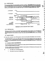
TABLE OF CONTENTS
-
~
-
.~
-
~
-
,~
Page
TABLE OF CO~S . . . . . . . . . . . . . . . . . . . . . . . . . . . . . . . . . . . . .
UST OF AGURES
UST OF TABLES
ABBREVlAllONS/MNEMONlCS
-
~
:
.~
-
-,
,
'
1.4.5 R~d/Write'Headsand Disk(s)
. . . . . . . . . . . . . . . . . . . . . . ..
.
.
.
.
.
.
.
.
.
.
.
.
.
.
.
.
.
.
.
.
System
n
Altratio
1.4.6 A1r
. . . . . . . . . . . . . . . . . . . . . . ..
.
.
.
.
1.4.7 Spindle Lock and Brake. . . . . . . . . . . . .
. ..
...
•
••
·
~
•
. .j
-
..
~.
I!I
'.
.
-.
•
'f8
. .
. . . . . . . ..
General Operation . . . . . . . . . . . . . . . . . . . . . . . . . . . . . . . . . . . .
ics
Electron
Control
and
Read/Write
1:1
I-I
1·1
1-2
1-2
1-2
1-2
1-3
1·3
1·3
1-4
. . . . . . . . .. 1-4
1.4.3 Drive Mechanism. . . . . . . . . . . . . . . . . . . . . . . . . . . . . . . . . . . . . . . . . . . .. 1-4
.
.
.
.
.
.
.
.
.
.
.
.
.
.
.
.
.
.
.
.
.
.
.
.
.
1.4.4 Positioning Mechan ism. . . . . . . .
'. . . . . .. 1-4
~
..
vi
vii
viii
viii
SECTION I ~ODUCT10N
...... ...... ...
1.1 Purp ose. ...... ...... ...... ...... ...... ...... ......
. . . . . . . . . . . . ..
.
.
.
.
.
.
.
1.2 General Description . . . . . . . . . . . . . . . . . . . . . . . . . . . . .
. . . . . . . . . . . . ..
.
.
.
.
.
.
.
.
.
.
.
.
.
.
.
.
1.3 Specifications Summmy . . . . . . . . . . . . . . . . .
. . . . . . . . . . . . ..
.
.
.
.
.
.
.
.
.
.
.
.
.
.
.
.
.
.
.
.
.
.
1.3.1 Perfonnanc~ Specifications. . .
. . . . . . . . . . . . ..
.
.
.
.
.
.
.
.
.
.
.
.
.
.
.
.
.
.
.
.
.
.
.
.
.
.
1.3.2 Functional Specifications.
. . . . . . . . . . . . . . . . . . . . . . . . . . . . . . . . . . . ..
1.3.3 Physical Specifications
. . . . . . . . . ..
1.3.4 Reliabtlrty Specifications
. . . . . . . . . ..
.
.
.
.
.
.
.
.
.
.
.
.
.
.
.
.
.
.
1.4 Functional Characteristics . . . . . . . . . . . . . . . . .
1.4.1
1.4.2
'.
•
ill
PROD UCTIO N DESCR IPTIO N
••
..
.
NOTICE TO USERS
i
:
.....
t
1-4
1-6
......
1.4.8 R~d/Write Head Shippin g Zone. . . . . . . . . . . . . . . . . . . . . . . . . . . . . . ..
..
.
.
.
.
.
.
.
.
.
.
.
.
.
.
.
.
.
1.5 Functional Operations
dng
Sequen
1.5.1 Power
1.5.2 Drive Selection
. . . . . . . ..
1.5.3 Track Accessing. . . . . . . . . . . . . . . . . . . . . . . . . . . . . . . . . . . . . .
. . . . . . . ..
.
.
.
.
.
.
.
.
.
.
.
.
.
.
.
.
.
.
.
.
.
.
.
.
.
.
.
.
.
.
.
1.5.4 Read Operation. . . . . . .
. . . . . . . ..
.
.
.
.
.
.
.
.
.
.
.
.
.
.
.
.
.
.
.
.
.
.
.
.
.
.
.
.
.
.
.
.
.
.
.
.
.
1.5.5 Write Operation.
1.5.6 Head Selection
1-6
1-6
. . . . . . . . . . . . . . . . . . . . . . ..
SECTION n ElECI'R.lCAL OOERFACE . . . . . . . . . . . . . . . . . . . . . . . .
2.1 Introduction
2.2 Control Input Unes
. . . . . . . ..
2.2.1 Drive Select 1-4. . . . . . . . . . . . . . . . . . . . . . . . . . . . . . . . . .. .. .. .. . . . . . . . ..
.
.
.
.
.
.
.
.
.
.
.
.
.
.
.
.
.
.
2.2.2 Direction In . . . . . . . . . . . . . . . . . . .
...... .
2.2.3 Step ...... ...... ...... ...... ...... ...... ...... ......
. . . . . ..
.
.
.
.
.
2.2.4 Head Select ~ and 2' . . . . . . . . . . . . . . . . . . . . . . . . . . . . . . . . . . . . . . . ..
.
.
.
.
.
.
.
.
.
.
.
.
.
2.2.5 Write Gate. . . . . . . . . . . . . . . . . . . . . . . . . . . .
2.2.6 Reduced Write Current and Precompensation
. . . . . . . . . . . . ..
2.3 Contro l O\Jtput Unes . . . . . . . . . . . . . . . . . . . . . . . . . . . . . . . . . . .. . . . . . . . . . . . . ..
.
.
.
.
.
.
.
.
2.3.1 Tr&ek 00 . . . . . . . . . . . . . . . . . . . . . . . . . . . . .
...... ..
2.3.2 Inde x.... ...... ...... ...... ...... ...... ...... ......
....
......
......
......
......
......
......
......
......
2.3.3 Rea dy..
2-1
Ul
1-6
1-6
1-7
1-8
1-8
1·8
2-1
2-2
2-4
2-4
2-4
2-5
2-6
2-6
2-6
2-6
2-6
2-6
TABLE OF CONTENTS (CONT.)
)
.
Wrtte Fault
.
·
·
·
·
·
·
.
·
·
·
.
·
· ..
·············
2.3.5 Seek Comple te
·
·
..
·
.
·
·
·
..
·
.
·
·
·
·
.
·
..
·
2.4 Data Transfer Unes
.
Data
Write
2.4.1 ~
.
2.4.2 ~ Read Data
······.····
·
·
2.5 Select Status
•••.. •..... ...... .
2.6 Genera l Timing ReqUirements ...... ...... .....• .....•
··.·.·····.·
2.7 Power Interface
········.·.·
·
·
·
·
·
2.8 Frame Ground ing
2-7
2-7
2-7
2-8
.
.
·
·
.
·
·
·
·
·
..
·
·.··
· · . · · . · .. · ·
· .. · · · · · · .. · · · · · · · · · ·
3-1
3-1
3-1
.
4-1
2.3.4
SECTION III
PHYSI CAL INTERFACE
3.1 Introduction
3.2 Jl!Pl Connec tion
3.3 J5/P5 Connec tion
3.4 J6/P6 Connec tion
·
PHYSI CAL SPEC IACAll 0NS
4.1 Mechanical Dimensions
4.2 Mounting
SECTION IV
SECTION V
·
2·9
3-2
3-2
· . · · · · · 4-1
'
·
2-8
2-8
2-8
2-9
4-2
.
. 5-1
. 5-1
MEDlA DEFECTS AND ERRORS
5.1 Error Mapping and Qualification
. 5-1
5.1.1 Cause.s of Errors
...... ...... 5-1
5.1.2 Error Definition ...... ...... ...... ...... ...... ...•.
. 5-1
5.1.3 Media Defed Definition
. 5-2
5.1.4 Error Map
5-2
.
5.1.5 User Error Mapping
. 5-2
5.2 Error Accept ance Criteria
. 5-2
5.3 System Genera ted Errors
SECTION VI
.
RECORDING FORM AT
6.1 Track Fonnat
6.2 Gap Length Calculations
6.2.1
Gap 1 . ~
6.2.2
6.2.3
Gap 2
I•
•
"• • • • • • • • • • • • •
••••••••
SECTION VII
••••••••••••
~
•••••
6-1
"• • • •
. 6-1
. 6-2
Gap 3
£ •••••••••
~
•••••••
••••••••••••••••••••
6.2.4 Gap 4
. 6.3
~
6-1
. 6-1
Write ?recom pensati on
6-2
. 6-2
. 6-2
. 7-1
. 7-1
. 7-2
CUSTOMER INSTA llABL E OPTIONS
7.1 FuU-Height Faceplate Kit
7.2 Low-Po wer Slow Start Jumper
OPER ATION S DESC RIPTIO NS
SECTION VIII
niEOR Y OF OPERAnONS
.•.... .•.•• ...... .....
8.1 Introdu ction .•••• •.•... •..... ...•.• .•••• •••••
ound)
8.2 High Priority Critical Tasks (Foregr
8.2.1 Foregro und Loop Control
. . . . . . . . . . . . . . ..
8.2.2 Spindle Motor Foregro und . . . . . . . . . . . . . . . . . . . . . . .
. . . . . . . . . . . . . . ..
.
.
.
.
.
.
.
.
.
.
.
.
.
.
.
.
.
.
.
.
.
.
.
.
.
und
8.2.3 Motor Fault Foregro
. . . . . . . . . . . . . . ..
8.2.4 Step Input Buffering Function . . . . . • . . . . . . . . . . . . . . .
. . . . . . . . . . . . . . ..
.
.
.
.
.
.
..
.
8.2.5 Stepper Damping Time Out Routine . . . . . . .
. . . . . . . . . . . . . . ..
.
.
.
.
.
.
.
.
.
.
.
.
.
.
.
.
.
.
.
.
.
8.2.6 Seek Function Foregr ound. .
. . . . . . . . . . . . . . ..
.
.
.
.
.
.
Return
t
Interrup
and
8.2.7 Foregro und End
. . . . . . . . . . . . . . ..
.
.
..
8.3 Lesser Priority Critical Tasks (Background) . . . . . . . . . . . . . .
. . . . . ..
8-1
8-1
8-2
8-2
8-2
8-2
8-2
8-2
8-3
8-4
8-4
8-5
.
.
.
.
.
.
.
.
.
.
.
.
.
.
.
.
.
.
.
.
.
.
8.3.1 System Startup Code . . . . . . . . . . . . . .
8-5
..
.
.
.
.
.
.
.
.
.
.
.
.
.
.
.
.
.
.
.
.
.
.
.
.
.
.
.
.
.
.
.
.
.....
8.3.2 Spindle Motor InltializZltion
tv
)
TABLE OF CONTENTS (CONT.)
,
8.3.3 Microprocessor Control Fault indicator Function
· . . . . . . . . . . . . . . . ..
8.3.4 . Seek Function lnitiallzZltion
·.···.·
~ . . . . . . . . . . ..
8.3.5 Inttialize Code End
· . . . . . . . . . . . . . . . . . . ..
8.3.6 Spindle Motor Background. . . . . . . . . . . . . . . . . . . . . . . . . . . . . . . . . . . . . ..
8.3.7 Motor Status Monitor. . . . . . . . . . . . . . . . . . . . . . . . . . . . . . . . . . . . . . . . . ..
8.3.8 Warm-up Settling Extension Countdown
· . . . . . . . . . . . . . . . . . . ..
8.3.9 System Background Loop Control
8.3.10 Loss of Index Monitor. . . . . . . . . . . . . . . . . . . . . . . . . . . . . . . . . . . . . . . . ..
8.3.11 CyUnder Address Rezero Monitor
8.3.12 Seek Ramping Calculate Function . . . . . . . . . . . . . . . . . . . . . . . . . . . . . . . ..
8.3.13 Drive Actuator Self-exerdse Function. . . . . . . . . . . . . . . . . . . . . . . . . . . . . ..
8.3.14 Actuator Lube Unstick Routine . . . . . . . . . . . . . . . . . . . . . . . . . . . . . . . . . ..
8.3.15 Automatic Actuator Reset to Track Zero (Recal Function)
8.3.16 Write Current Control Function. . . . . . . . . . . . . . . . . . . . . . . . . . . . . . . . . ..
8.3.17 Drive Select LED Monitor . . . . . . . . . . . . . . . . . . . . . . . . . . . . . . . . . . . . . ..
8.3.18 Background Code End
' . . . . . . . . . . . . . . . . . . . . . ..
8.4 System Initialization Tasks. . . . . . . . . . . . . . . . . . . . . . . . . . . . . . . . . . . . . . . . . . . . ..
8-7
8-7
8-7
8-7
8-7
8-7
8-8
SEcnON IX PACKAGING INSTRUcnONS
9. 1 Uncrating.........................................................
9.2 Recommended Receiving Inspection . . . . . . . . . . . . . . . . . . . . . . . . . . . . . . . . . . . . ..
9.2.1 Packaging and Identification . . . . . . . . . . . . . . . . . . . . . . . . . . . . . . . . . . . . ..
9.2.2 Mechanicallnspeetion
9.2.3 Functional Testing
,. . . . . . . . . . . . . . . . . . . ..
9.3 Packing for Reshipping. . . . . . . . . . . . . . . . . . . . . . . . . . . . . . . . . . . . . . . . . . . . . . ..
9-1
9-1
9-1
9-1
9-1
94
9-4
SEcnON X
~8
8-8
8-8
8-8
8-8
8-8
8-9
8-9
8-9
8-9
DRIVE INTERCONNECT . . . . . . . . . . . . . . . . . . . . . . . . . . . . . . . . . . . . . . . . . . . . . . . . . . . 10-1
SERVICING INFORMATION
SEcnONXI
SPAREPARTS
11-1
11.1 Routine Order Entry. . . . . . . . . . . . . . . . . . . . . . . . . . . . . . . . . . . . . . . . . . . . . . . . . 11-1
11.2 Emergency Order Entry
'
'
,.11-1
SEcnON VII
MAINl"'ENANCE
12.1 Introduction
12.2 Maintenance Equipment. . . . . . . . . . . . . . . . . . . . . . . . . . . . . . . . . . . . . . . . . . . . . .
12.3 Diagnostic Techniques
12.4 Test Point Locations
12.5 Troubleshooting
12.6 Checks and Adjustments
12.7 Removal and Replacement Procedures
12.7.1 Removal of Control PCB
..............................
12.7.2 Replacement of Control PCB
12.8 Alignment Procedures
12.9 Preventive Maintenance
SEcnON XIII
ILLUSTRATED PARTS CATAlOG . . . . . . . . . . . . . . . . . . . . . . . . . . . . . . . . . . . . . . . . . . 13-1
13.1 De-scription....................................................... 13-1
13.2 Indented Level
13-1
13.3
t
12-1
12-1
12-1
12-1
12-1
12-1
12-2
12-4
12-4
12-4
12-5
12-5
Quantity per Assembly . . . . . . . . . . . . . . . . . . . . . . . . . . . . . . . . . . . . . . . . . . . . . . . 13-1
13.4 Recommended Spare Parts Stocking Guide . . . . . . . . . . . . . . . . . . . . . . . . . . . . . . . . 13-4
SEcnON XN
SCHEMATIC DIAGRAMS
14-1
APPENDICES
APPENDIX A ORDERING INFORMATION
A·l
v
LIST OF FIGURES
)
Figure
I-I
1-2
1-3
1-4
1-5
2-1
2-2
2-3
2-4
2-5
2-6
2- 7
2-8
2-9
2-10
2-11
3-1
3-2
3-3
3-4
4-1
6-1
7-1
7-2
7-3
8-1
8-2
8-3
9-1
9-2
10-1
12-1
12-2
13-1
13-2
14-1
Title
Page
Shugart 706/712 Rigid Disk Storage Drive
Read/Write Head Positioning Mechanism
AIr Filtration System ·
Spindle Lock
Shipping Zone
J51nterface and Jl Power Connections. . . . . . . . . . . . . . . . . . . . . . . . . . . . . . . . . . . . . . . . . ..
J61nterface Connection
Control Input Driver/Receiver Combination
Jumper Locations ....
Normal Step Mode ..
Buffered Step Mode .
Head Selection Timing o.
Index Timing.
Data Transfer Line Driver/Receiver Combination ...
MFM Read/Write Data Timing ....
General Control Timing Requirement
Interface Connector Locations
Jl Connector
J5 Connector Dimensions
J6 Connector Dimensions
Mounting Dimensions
~ . . . . . . . . . . . . . . . . . . . . . . . . . . ..
Track Format
Full-Height Faceplate Kit. . . . . . . . . . . . . . . . . . . . . . . . . . . . . . . . . . . . . . . . . . . . . . . . . . . . ..
Low Power Option (Early Models) . . . . . . . . . . . . . . . . . . . . . . . . . . . . . . . . . . . . . . . . . . . . . ..
Jumper Installation and Fabrication. . . . . . . . . . . . . . . . . . . . . . . . . . . . . . . . . . . . . . . . . . . . ..
Logic Diagram
Foreground Routines Sequencing . . . . . . . . . . . . . . . . . . . . . . . . . . . . . . . . . . . . . . . . . . . . . ..
Background Routines sequencing
Single Unit Packaging Configuration . '
~ ..
Ten Units Packaging Configuration
. . . . . . . . . . . . . . . . . . . . . . . . . . . . . . . . . . . . . . . . ..
Multiple Drive Configuration
Locations Diagram
Removal/Replacement of Control PCB
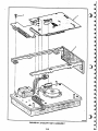
Shugart 706/712 Assembly
Front Panel and Rail Assembly
Control PCB Schematic (2 Sheets)
0
0
•
0
0
•••••••••••••
•••••••••••
0
0
••
0
0
•••
0
•••
•
0
••••••••••••
••••
0
••
••••
•••••••
0
0
•
0
0
••
•
•
•
•
•
••
0
•••
0
•
•
•
•
•
•
•
•
•
•
•
•
•
•
••
•
•
•
•
•
•
•
•
•
•
•
•
•
•
•
•
•
•
•
•
•
•
•
••
0
•
•
••••
0
•
•
•
•
•
•
•
•
•
•
•
•
•
•
•
•
•
••
•
•
•
•
•
•
•
•
•
•
•
•
•
•
•
•
•
•
•
•
•
•
••
•
•
•
•
•
•
•
•
•
•
0
•••••
••
0
•
0
0
•
•
•
•
•
•
0
••
•
•
0
••••
•
0
•
o
•
•
•
•
•
•
•
•
•
•
0
0
••••••••••
0
•
•
•
•
•
•
•
•
•
•
•
•
•
••
0
0
•
•
•
•
•
•
•
•
•
•
•
•
•
•
•
•
•
•
•
•
•
•
•
•
•
••
•
•
•
•
•
•
•
•
•
•
•
•
•
•
•
•
•
•
•
•
•
•
•
•
•
•
•
••
0
0
•••
0
•••••••
0
•••••••
0
•
•
•
•
••
0
•
•
•
•
•
•
•
••
0
0
•
••••••••
•
0
•
0
0
••
••••
0
•••••
••••••••
0
•••
0
••••
•••••••
0
•
•
•
•
••••••••••••••
0
•
0
••
•
•
•
•
0
••••
0
•••
•••••••••••
••••••••
•
0
••••••••••••
0
•
•
••••••
•••••
•
•
••••••••
0
•
•
••••••
0
0
•
•
••
0
•
0
•
0
••••••
•
0
0
0
•
•
•
0.0
•••
•
•
0
0
•
•••••
0
0
•
•
0
••
•
0
•••
0
0
•
0
•
•••
•
•
•••••••••
0
0............
0
•
•
•••••••
0
•••••••••••••••
0
•
••••••••••
0
0
0
••••••••••••••••••••••••
0
0
0
0
••••
0
0
••
0
•
0
•
•
0
•
•
•
•
•
•
•
•
•
•
••••••••••••••••••
0
0
•
•
•
•
•
•
•
0
•••••••
•
•
•
•
•
•
•
•
•
•
•
•
•
•
•
•
•
•
•
••
0
•
•
•
•
•
•
•
•
••
•
•
•
•
•
•
•
•
•
•
•
•
••
0
•
•
•
•
•
•
•
•
•
•
•
••
•
•
•
•
•
•
•
•
•
•
•
•
•
••
0
••••••••••••
• • • • • • • • • • • • • • • • • '.
•
•
•
•
•
•
•
•
•
•
•
•
•
"
••
0
•• '.
•
•
•
•
•
•
•
•
•
•
•
•
••
•
•
•
•
•
•
•
•
•
•
•
•
•
•
••
0
•
•
•
•
•
•
•
•
•
•
•
••
•
•
•
•
0
••••••••••
••••••••••••••••••••••••••••••••••••••••
I-a
1-5
1-5
1-6
1-7
2-1
2-2
2-3
2-3
2-4
2-5
2-5
2-6
2- 7
2-8
2-9
3-1
3-1
3-2
3-2
4-1
6·1
7·1
7-2
7-2
8-1
8-3
8-6
9-2
9-3
10-1
12-3
12·4
13·2
13-3
14-3
-.-•
.. I
-
•
,
"-,
- .... I
-
•
LIST OF TABLES
t
-. •
- -•
Table
.
2-1
-
-- "
2-2
6-1
8-1
8-2
~
-
-a
-
-
9-1
9-2
-- -•
-- -
12-1
..
12-2
12-3
13-1
A-I
~
Page
Tltl.
. . . . . . .. 2-5
False. 0 = True) · · · · · · · · . · . . . . . . . . . . . . . . . . . . . . . . . . . . . .
Head Select (1
· · . . . . . . . . . . . . . . . . . .. 2-9
DC Requir ements · · · .. · · · . · . · · · · . · · · . · · - ·
· . . . . . . . . . . . . . . . . . .. 6-2
Write Precom pensati on · · · · · · · . · · . · . · · . · · ·
. . . . . . . . . . . . . . . . . . .. 8-4
.
.
.
.
.
.
.
.
.
.
I/O Port Configuration .. · · . · · · · · · · · · · · · · · · · . . . .
· · . . . . . . . . . . . . . . . . .. 8-7
·
·
· · · · .. · · · · · · · · ·
LED Fault Codes . ·
· . . . . . . . . . . . . . . . . . . . . . . . . . . . . . . . . . . .. 9-4
·.··.···
·
Print Parame ters
...... ...... ...... ... 9-4
Test Progra m -.... ...... ...... ...... ...... ...... ......
12-1
PCB Versus Drive Failures
12-2
Inspection of the Drive
12-2
Signals Inspection
13-4
Shugar t 706/71 2 Spare Parts Stocking Guide
A·I
,
Shugar t 706/71 2 PSI .. ·
=
--
•
- ••
•
.•
.
-
..
-
--
••
...
-- ...-
.
;'
- •
--
.
-- .:.
~
-
.~
-
.~
---
.~
~~
--
,~
--
I~
,
~
-- ~
--
.~
vii
ABBREVIATIONS /MNEMONICS
BKPC
Background Port C
MFM
Modified FM
bpi
Bits per Inch
MLC
Machine Language Code
eRe
Cyclic Redundancy Check
PCB
Printed Circuit Bo.ard
0
Prompt Character
pp
Print Parameters
fel
Flux Change per Inch
PWM
Pulse Width Modulation
10
Identification
RCFLG Recalibrate Rag
I/O
Input/Output
R/W
Read/Write
IP
Inspect Phase
SEL
Select
LED
Light Emitting Diode
tpl
Tracks per Inch
LSI
Large
TRK
Track
~ale
Integration
NOTICE TO USERS
This manual, P/N 39402-0, supersedes, replaces, and incorporates the OEM manual. P/N 39252-1, published
April. 1983. and further includes the Publication Change Notice No. 1 dated August 18. 1983. and Publication
Change Notice No.2 dated February 20, 1984. All technical changes have been indicated with a change bar in the
text margin or a star symbol in the illustration. While every effort has been made to ensure that the information provided herein is correct, please notify us in the event of an error or inconsistency. Direct any comments on the form
at the back of this manual to:
Shugart Corporation
Technical Publications. MS 3-14
475 Oakmead Parkway
Sunnyvale, CA 94086 (U.S.A.)
Phone (408) 737-7900
Shugart makes no representations or warranties with respect to the contents hereof and specifically disclaims any
implied warranties of merchantability or fitness for any purpose.
Further, Shugart reserves the right to revise this publication and to make changes from time to time in the contents
hereof without obligation to notify any person of such revisions or changes.
The information contained herein has been copyrighted by the Shugart Corporation. No portion of this document
can be duplicated in any form, or sold, without the express written consent of Shugart Corporation. Failure to comply could entail legal action to remedy such violation.
viII
- '"
- 3
}
:
,
.~
SECTION I
INTRODUCTION
=I~
: ·3
I~
:
::
;~
-~
3
..
~
1.1
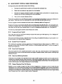
This publication is designed as a reference source for OEM engineers. system Integrators. service and maintenance
technicians. and knowledgeable end users. It is assumed that the reading audience is sufficiently versed in the stateof-the-art with respect to rigid disk drives .
1.2
:3
..
.,
.
--
t
The 706/712 interface is either ST506 or ST412 compatible, allowing easy integration into existing systems. Some
of the key features of this series are as follows:
~
:!
.~
I
~:
.:
.'.
.~~
: J
--
I
Low cost and high reliability are acheived through the use of a unique rotary band actuator design, a self-contained
microcomputer. and custom LSI circuitry .
.3
j
GENERAL DESCRIPTION
The Shugart 706/712 Disk Drives are random access 5.25 inch (130 mm) Winchester storage devices with one
(706) or two (712) non-removable disks as storage media. Ellch disk surface employs one movable head to service
320 data tracks. These drive are available in half-height or fun height configurations.
.- :3
~
PURPOSE
a.
Microprocessor-based electronics.
b.
Three custom LSI devices for reliability.
c.
BuUt-in diagnostics.
d.
Jumper selected exercise routines.
e.
Dedicated landing zone.
f.
Single track seek time is less than latency.
g.
Read/write pre-amp on head arm.
h.
3370 head flexure design .
l.
Brushless dc spindle motor.
j.
Winchester design reliability In a half-height or fun-height package.
k.
Improved shock and vibration characteristics.
-
~,
--:,
-
,~
1-1
... -.
"----'
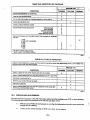
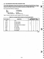
1.3 SPECIFICATIONS SUMMARY
1.3.1
Performance Speclflcatlona
Capacity
Unformatted
Per Drive
Per Surface
Per Track
Formatted (33 sectors/track)
Per Drive
Per Surface
Per Track
Per Sector
Formatted (32 sectors/track)
Per Drive
Per Surface
Per Track
Per Sector
Transfer Rate
Access Time (includes settling time)
Track to Track
Average
Maximum
I
Average Latency
706
712
6.4 Mbytes
3.2 Mbytes
10,416 bytes
12.7 Mbytes
3.2 Mbytes
10,416 bytes
5.2 Mbytes
10.3 Mbytes
2.6 Mbytes
2.6 Mbytes
8.4 kbytes
256 bytes
8.4 kbytes
256 bytes
5.0 Mbytes
10.0 Mbytes
2.5 Mbytes
8.2 kbytes
256 bytes
5.0 Mbits/sec
2.5 Mbytes
8.2 kbytes
256 bytes
5.0 Mbits/sec
16.2 msec
16.2 msec
85 msec
85 msec
175 msec
175 msec
8.37 msec
8.37 msec
12 sec
12 sec
2
1
320
4
Start Up Time (typical)
1.3.2 Functional Specification.
Read/Write Heads
Disks
Cylinders
Data Tracks
Index/Revolution
-I Rotational Speed
Recording Density
Aux Density
Track Density
Data Encode Method
Write Precompensation
Reduced Write Current
I Shipping Zone (track number)
I
2
320
1,280
640
1
3.600 (±0,-72) rpm
9.036 bpi
9.036 fci
360 tpi
MFM
12 (± 2) nsec
Automatic
353
1.3.3 Phy.lcal Speclftcatlon.
Mechanical Dimensions without Faceplate (nominal):
Height = 1.63 in ( 4.14 cm)
Width = 5.75 In (14.61 cm)
Depth = 8.00 In (20.32 cm)
Weight
3.0 Ibs { 1.36 kg)/706
3.6 Ibs ( 1.63 kg)/712
=
1-2
1.3 SPEC lFlCAn ONS SUMMARY
1.3.1 Pafor maace SpecUicadoD8
Capacity
Unformatted
Per Drive
Per Surface
Per Track
Formatted (33 sedon/ track)
706
712
6.4 Mbytes
3.2 Mbyte.
10,416 byte_
12.7 Mbytes
3.2 Mbytes
10,416 bytes
5.2 Mbytes
2.6 Mbytu
8.4 kbytes
256 bytes
10.3 Mbytes
2.6 Mbytes
8.4 kbytes
256 bytes
5.0 Mbyte.
2.5 Mbyta
10.0 Mbytes
2.5 Mbytes
Per Drive
: Per Surface
Per Track
Per Sector
Formatted (32 seeton/track)
Per Drive
Per Surface
Per Track
Per Sector
8.2 kbyta
I
8.2 kbytes
256 bytes
256 bytes ·
Transfer Rate
5.0 Mbltl/sec
5.0 Mbits/sec
Access Time (includes settling time)
Track to Track
Average
Maximum
16.2 msec
85maec
175 mMe
16.2 msec
85 msec
175 msec
Average Latency
8.37 maec
8.37 msec
12 He
12 sec
2
4
2
320
Start Up Tune (typical)
1.3.2 . Functi onal Specif icatio n.
Read/W rite Heads
Disks
Cylinders
Data Tracks
Index/Revolution
I Rotational Speed
Recording Density .
Aux Density
Track Density
Data Encode Method
Write Precompensation
Reduced Write Current
I Shipping Zone (track number)
I
1 .
320
640
1.280
1
3,600 (:0,-7 2) rpm
9,036 bpi
9,036 fd
360 tpi
t
MFM
, 12 (± 2) nsec
Automatic
353
1.3.3 Pbplc al Speclf tcatloD a
Mechanical Dimensions without Faceplate (nominal):
Height • 1.63 in ( 4.14 cm)
Width = 5.75 In (14.61 em)
Depth
=
8.00 In (20.32 em)
Weight = 3.0 Ibs ( 1.36 kg)/706
3.6 Ibs·( 1.63 kg)/712
)
1·2
.~
~
,...-
.... .j
,
~
....'.9
.. .oj
... Ij
.
,
Host Ambient Temperature:
Operating - 41 ° to 113°F (5° to 45°C)
Non-operating - _40° to 140°F (_40° to 60°C)
Temperature Gradient:·
.
Operating - 10°F (5.~OC) per 1/2 hour
Non-operating - 212°F (100°C) per hour non-condenllng
~
..- .~!t
--- .,
--
Relative Humidity:
Operating - 8% to 80%
Non-operating - 1% to 959.»
Maximum Wet Bulb:
Operating - 78°F (25.6°C) non-eondenslng
Non~operatlng - Non-eondenslng
~,
~!
-- •
--
Environmental Umtts:
Elevation:
.
Operating - 0 to 10,000 ft (0 to 3048 m)
Non-operating - -1.000 to 30,000 ft (-305 to 9144 m)
.o~
-- ••
Acoustic Noise: Less than 50 dbA at 3.3 It (1.0 m)
-. .:~
Shock:
10 G max (11 msec half sine wave)
Non-operating - 40 G max (11 msec half sine wave)
Vibration:
Operating -
•
Operating:
.:~
•
!I
5 - 17 Hz
17 - 150 Hz
200 - 500 Hz
Non-operating:
5 - 22 Hz
44- 500 Hz
= 0.036 In
= 0.55 G
:: 0.25 G
= 0.50 G
= 2.00 G
Oil
·
-
~CI
·
: ~ II
DC Voltage Requirements:
.
± 12 Vdc ± 5% .75 A typical (3.9 A max starting for 10 sec) (2.7 A max starting with low power option)
± ·5 Vdc ± 5% 1.6 A typical (2.4 A max)
I
- d'
·
\1
°
·· ,.u·
·· .,
\~
Heat Dissipation
.
= 86 BTU/hr typical (18.4 watts)
1.3.4 Reliability Speclflcatlona
Mean Time Between Failure:
Preventive Maintenance:
Mean Time to Repair:
Component ute:
20,000 Power-on Houn typical usage
None Required
12 minutes (PCB only)
I
5 yean
1.4 FUNCTIONAL CHARACTERISTICS
·· Do·
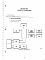
1.4.1 General Oper.dOD
· :.L·
The 706/712 fixed disk drives consist of read/writ., heada, read/write and con;ol electronics, track positioning
· .,
·· --
mechanisms, media, and air filtration systems. TheM components perform the foUowing functions:
~l
-- .,-I
·. .: 4
"
•
~:
"
i
..
a.
Interpret and generate control signals.
b.
Position the heads over the seleded track.
c.
Read and write data.
d.
Provide a contaminant-free environment.
. '~-
. ,-
1·3
--
.~
1.-4.2 Read/Write anel Control Electroalea
The standard ~iaoproceS50r and electronics are packaged o~ one printed circuit board containing the foUowing
circuits:
a.
Index Generator Circuit
b.
Head Position Actuation Drivers
c.
Read/Write Amplifiers
d.
Drive (READY) up to Speed Circuit
e.
Drive Select Circuit
f.
Write Fault Detection Circuit
g.
Read/Write Head Select Circuit
h.
Ramped (Buffered ) Stepper Circuit
I.
Track 00 Indicator
j.
Brushless Spindle Motor Control Circuits
1.4.3 Drive Mechanlam
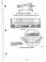
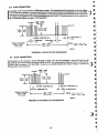
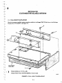
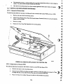
I The brushless dc drive motor rotates the spindle at .3.600 (:t 0, - 72) revolutions per minute.
1.4.4 Poaltlonlng Mechanl••
The read/write heads are mounted on an arm which is positioned by I Fasflex™ IV rotary actuator. A stepper
motor is used to precisely position the rotary actuator utilizing a unique metal band/capstan concept. Figure 1-2 ulustrates thiS positioning mechanism.
.
1.4.5 Read/Write Head. and DI.k(l)
The recording media consists of a thin, lubricated, magnetic oxide coating on a 130 mdUmeter diameter aluminum
substrate. This coating formulation, together with the low load force/low mass Winchester-type flying heads, permits reliable contact stan/stop operation.
I Data on each disk surface are read by one read/write head, each of which accesses 320 data tracks. The drive is
available in two basic configurations: one disk with two read/write heads (706) or two disks with four read/write
heads (712). The heads should be positioned at cybnder 353 via IOftware prior to power down in order to minimize
the potential for damage to the recorded data on portable systems. Refer to paragraph 1.4.8.
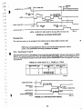
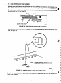
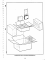
1.4.6 AIr flltratioD Syatem
The disk(s) and read/write heads are fuUy encased In a protective cover using an integral recirculating air system,
with a recirculating filter. to maintain a contaminant-free environment. A separate absolute breather filter allows
pressure equalization within the envelope to the ambient air without contamination. See figure 1-3.
.
)
'-4
ACTUATOR
SPINDLE ASSEMBLY
BAND
PJW HEAD
ASSEMBLY
*
STEPPER
.MOTOR
FIGURE 1·2. READ/WRITE
HEAD POSITIONING MECHANISM
0.3 MICRON
BAROMETRIC
FILTER
. COVER
*
CAPSTAN
0.3 MICRON
FILTER
FIGURE 1·3. AIR FILTRATION SYSTEM
1·5
1.4.7
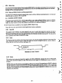
, Spindle Lock and Brake
These drives are provided with an integral fall·sal. spindle lock and brake. ThIs lOIenold operated. mechanical
brake is actuated when de power is applied to the drive, allowing the spindle to rotate. When the drive is powered
off, the solenoid is deae:ttvated allowing the brake to engage the spindle. This prevents the possibility of disk move·
ment during shipping or movement of the drive. During spin down, the brake decelerates the spinning disks quickly
to reduce the amount of time that the heads are In unltable flight. Se. figure 1-4.
)
BRUSHLESS DC
SPINDLE MOTOR
STEPPER MOTOR
FIGURE 1-4. SPINDLE LOCK
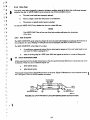
1.4.8 Read/Write Head Shipping Zoae
The unused area of the disk surface. Inside the data bands, is designated as a "shipping zone." The heads should be
positioned to this area via software before the drive 15 powered off. prior to moving or shipping the drive. This ensures that if the drive is exposed to severe handling (shock). the data storage area of the disk surface will not be
damaged by heads movement on the disk(s). See figure }-5.
1.5 FUNCTIONAL OpERATIONS
1.5.1 Power SequencIDl
The required power-on sequence for early production units (1.8., 706/712 that are MLC 4 or less) is that both the 5
and 12 volts supplies be on" within 20 seconds of each other. The order is not important.
M
No power-on sequence is required for MLC 5 and above. All drtves have a speed sense ctrcult to prevent stepping
until the disk is rotating at the proper speed (3,600 rpm). A READY signal will be presented to the controller interface once the disk is up to' Its normal rotational speed (:t 2%) for two seconds. At .READV time, after an initial
power-up, the drive will recalibrate Itself to track 00. When the recallbration procedure Is complete. SEEK COMPLETE will go true. Normal seek and read functions can now begin. Refer to paragraph 2.6.
!
·1.5.2 Drive SelectlOD
l
i
)
Drive selection occurs when one of the DRIVE SELECT Ilnes II activated. Only the drive appropriately jumpered
will respond to the input signals. and the output signals of that drive are then gated to the controller.
1·8
130 mm
DISK 00
- DATA
TRt< 00
TRACKS
.'@
....
:~
-- .....
: .. ~
-
.:1
•
lJ
.,
"
u
.
"
I,
..
· l
.• l
HEAD SHIPPING ZONE
40mm
CYLINDER 353
DISK 10
FIGURE 1·5. SHIPPING ZONE
._'
1.5.3 Track Acceaalng
.. ,
Read/write head positioning is accomplished by:
a.
Deactivating the WRITE GATE.
.. ,
b.
Activating the appropriate DRIVE SELECT line.
,
c.
Being in the READY condition with SEEK COMPlETE true.\
d.
Selecttng the appropriate direction.
e.
Pulsing the STEP Un•.
f.
Checking for the edge of the -SEEK COMPLETE line (changing from false to true).
I
t
.'
..
•
t• . '
.. ,
·
...
(t
......
Stepping can occur at either the normal or buffered rate. DUring normal stepping,-the heads are repositioned at the
rate of incoming step pulses. In the case of buffered stepping, Incoming step pulses are received at a high rate and
are buffered Into counters. When all of the steps have been received, they are Issued to the stepper drivers at a
ramped stepping rate.
Each pulse will cause the heads to move either one track In or one track out, depending on the level of the DIRECTION IN line. A true on the DIRECTION IN line wUI cause an Inward seek: a false will result in an outward seek
toward track 00.
.
t'
'·7
1.~4
Reacl OperaUoUl
Reading data &om the d1sk Is accompUshecl by:
a.
Deactivating"the WRITE GATE line.
r
b.
Activating the appropriate D~ SELECT line.
c.
Assuring that the drive
d.
Selecting the appropriate head.
ts READY.
1.5.5 Write Operation
Writing data
onto the disk is accomplished by:
a.
Activating the appropriate DRIVE SELECT Une.
b.
Assuring that the drive is READY.
c.
Clearing any write fault conditions (if that exist). by reselceting the drive.
d.
Selecting the proper head.
e.
Activating the WRITE GATE and plactng data on the WRITE DATA Un••
1.5.6 Head Selection
Any of the two to four possible heads can be seleded by placing the binary address of that head on the two HEAD
SELECT Unes.
)
\
~
1·8
t
-
J
· .J
•
•
.J
•
.1
:
-'
:
:~
,
SECTION II
ELECTRICAL INTERFACE
2.1 INTRODUCTION
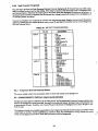
The interface for a 706/712 has drive control signal pin ualgnmentl per Industry standards. See figure 2·1 for the
pin assignments.
7OeI712
,
HOST
•
RESERVED
l.
-
RESERVED
.1
..
-WRITE GATE
-SEEK COMPLETl
2
3
-•
-•
5
7
•
~
1
-TRACK 00
t
10
"
(.
I'
13
-- t.
15
-
11.
17
'1
11
-WR'TE FAULT
.1
-
-HEAD SELECT 2'
RESERVED
'.
FLAT
tC
AlIBON
-HEAD SELECT
20 FT. MAX.
ce"mm)
-•
,r
-
2' •
-
-INDEx
~
-~EADY
a
•
I
-DAIVE SELECT t
·· .".
·· '-'.
-DRIVE SILECT 2
-DAIVE IllECT 3
·. -'
.,.
- DRIVI SILECT •
,.
-DIRECTION IN
·• ',a.
-
..£:
·"
--..
• ~ v DC
A
• ~ RETURN
• '2 Y DC
• 12 RETURN
--X
-
..
•
-•
•
•
N
-
a
25
zr
-•
--
21
3D
31
-- 3Z
33
-•
3
-
2
- ,.
1
.
..,,1P1
rh--=-
rJ
GND
*
-
23
~
DCGNO
•
~
22
.r
-STEP
•
-
~~
TWISTED PAIR
IfRAUEGND
FIGURE 2·1. J5 INTERFACE AND J1 POWER CONNECTIONS
2·1
The sJgna11nterface consists of three categories:
I
a.
Control Input Una
b.
Control Output Una
c.
Data Transfer Una
AD control lines are digitalin nature and either provide signals to the drive (input) or provide signals to the host (output) via the interface connector JS/P5. The data transfer slgnall are differentialln nature. They provide data either
to or from the drive. via J6/P6. See figure 2-2 for the J6/P6 pin assignments.
706n12
HOST
- DRIVE SELECTED
GND
-
1
SPARE
3
GND
SPARE
5
GNO
RESERVED
7
GND
SPARE
GND
GND
GND
+ MFM WRITE DATA
-MFM WRITE DATA
GND
GND
+ MFM READ DATA
-MFM READ DATA
FLAT CABLE
20 FT MAX
(8.6 mm)
---
GNO
,
2
~
8
J6/Pe
8
10
'1
12
-
- ,..
13
17
18
GND
--:
15
16
)
19
20
-..
~
*
FIGURE 2·2. J6 INTERFACE CONNECTION
2.2 CONTROL INPUT UNES
The control1nput signals are of two types; those Intended for multiplexing In a multiple drive system, and those intended to control the multiplexing. The controllnput Ilgnals to be multiplexed are:
a.
The STEP signal
b.
The DIRECTION SELECT signal
c.
The HEAD SELECT 20 and 2 1 signals
d.
The WRITE GATE signal
The signals which are intended to control the multiplexing are DRIVE SELECT 1 through DRIVE SELECT 4.
The controllnput lines have the following .lectrical specifications. 541. figure 2-3 for the recommended cIrCuit.
Only one drive In the system should be terminated. h should be located at the end of the cable and terminated with
a 220/330 ohm resistor pack. This resistor pack can be disabled by removing the jumper block located near the P5
connector. See figure 2-4 for the location.
)
t
l
t
--
i
....
~ l·~
-
20 FT (MAX)
(6.0 mm)
...
")
~l .. !
t
-.
.. ...
~
:
~
---
.. ill
.~
True
False
-- •
-- .•
-- •.
-=-
0.0 to 0.• V de fl lin = .0 mA (max)
lin
0 mA (open)
= 2.5 to 5.25 V de "
--
=
3i026-06·A
FIGURE 2·3. CONTROL INPUT DRIVER/RECEIVER COMBINATION
~
-
.~
--
...
-
.
• C!I
REAR VIEW
.1
-- ..tI
•
II
-
II
DRIVE SELECT.
· .
-
·• a.
•
•
'II
....
3./.
UNDEFINED
WRITE GATE
HEAD SELECT 21
DRIVE ALWAYS
NOTE:
These eight Jumper. are for
5 LECTED
drive control line termination and .r.
to be removed from ai, but the Int
drive in a multiple drive configuraUon
(r.fer to Section IX).
*
UNDEFINED
DIRECTION
HEAD SELECT 2'
STEP
FIGURE 2·4. JUMPER LOCATIONS
·.
• ' .. =!I
·· .-
~
- .,
.. ,
UNDEFINED
DRIVE SELECT
j
DRIVE SELECT 2
DRIVE SELECT 1
II
•
I/
2·3
2.2.1
.. DrIve Select 1-4
DRIVE SELECT, when logically true, connects the drive to the control Una. Only one DRIVE SELECT line may
be active at a time.
)
Jumper options 051-4 are used to choose which DRIVE SELECT lin. wID activate the Interface for that unique
drive. See figure 2-4 for the jumper locations.
.
2.2.2 Direction 10
This signal defines the direction of motion of the read/write heads when the STEP bne Is pulsed. An open ctrcult, .
or logical false. defines the direction as "out" and a pulse applied to the STEP lin. wID move the R/W head away
from the center of the disk. Uthe Input is shorted to ground (logical true) and a pulse is applied, the heads wID move
toward the center of the disk. I.e. ''In.,.
2.2.3 Step
This line causes the read/write heads to move In the direction defined by the DIRECTION IN line. The motion Is initiated at each logical true-ta-false transition. Any change In the DIRECTION IN line must be made before the
leading e ige of the STEP pulse. Stepping can be performed in lither the normal or buffered mode:
Normal Step Mode
In this mode. the read/write heads will move at the rate of the Incoming STEP pulses. The minimum time between
"'
successive steps is 3.0 msec, with a minimum pulse width of 500 nsec. See figure 2-5.
-DIRECTION
~
I
-STEP
1'00
,nslC MIN'
~I
*
1I
)
3.0maec MIN
I
I
--.,
~1oon"CMIN
I-
J
-SEEK COMPLETE
•
(5141215T5OI TYPE UO)
p550nsecTYP
~·'3-A
FIGURE 2·5. NORMAL STEP MODE
Buffered Step Mode
In this mode, the STEP pulses are received at a high rate and buffered Into a counter. After the last STEP pulse. the
read/write heads will begin stepping the desired number of cylinders and SEEK COMPlETE (refer to paragraph
2.4.5) will go true after the heads settle on the cylinden. This mode of operation is automatically selected when the
between STEP pulses is less than 200 pee.
. .
time
The DRIVE SElECT line may be dropped and a different drive selected 500 nsec after the last STEP pulse has
been sent to the drive.
The maximum time between steps
is
200 1d8C. with a minimum pulse width of 3.0 ~. See figure 2-6.
)
2·4
--
:
.
-.
-STEP
:
_I
...
:
-SEEK COMPLETE
-DRIVE SELECT X
NOTE:
: '.'
VARIES WITH SeEK L~NGTH. 11•• mMC MIN, .a.o maec MAX.
FIGURE 2·8. BUFFERED STEP MODF
Shipping Zone
: ..'
•
The read/write heads can be accessed to the shipping zone by doing. seek to cylinder 353.
NOTE
STEP pulses with periods between 200 "sec and 3.0 msec are not permitted. Seek accuracy is not guaranteed If. this timing requirement is violated.
u
.1
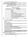
2.2.4 Head Select 2- and 2 1
These two lines provide for the selection of each individual read/write head In a"binary coded sequence. HEAD
SELECT 2° is the least significant line. When all HEAD SELECT 11nes are false, head 0 will be seleded. Table 2·1
shows the HEAD SELECT sequence and model variations for the HEAD SELECT lines. See figure 2-7 for the tim-
· u
ing
sequences.
,"
TABLE 2·1. HEAD SELECT (1
• u
•
II
•
u
•
\t
·
\
!
HEAD SELECT LINE
20
21
1
0
1
0
1
1
0
0
= FALSE, 0 = TRUE)
HEAD SELECTED
701
HEAD SELECTED
712
0
0
1
2
3
1
IMPROPER SELECT
IMPROPER SELECT
•• l
I
HEADS SWITCHED
··'-'
READ DATA
•
·-
VAUD
•• 1
·•• -I
• !
.. ,
+ WRITE GATE
WRITE DATA
(FROM CONTROLLER)
VALID
-...-..--...1
-.f ~
-.-.-_1
8 "lee MAX
l
- .....-
'1
....1
~ ~
_ _ _ _I
400
I
~( FORMAT SENSITIVE)
naec MAX
1-._ _
FIGURE 2·7. HEAD SELECTION TIMING
•••
2·5
8 "aec
I
f
')
2.2.5 Write Gate
I
The active state of this signal (logical 0 level) enables WRITE DATA to be Written onto the disk. The inactive state of
the signal (logical 1 level) enables data to be transferred from the drive and STEP pulses to reposition the head arm.
See figure 2-7 for the tlm1ng sequences.
I
~I
2.2.6 Reducecl Write ClII1'eDt and Precom,...AtloD
f
The 706/712 provides for automatiC reduced write current switching. Optimum precompensation 15 12 nsec and
should be used on cyUnders 128 through 320.
I
2.3 CONTROL OUTPUT UNES
I
The control output signals are driven with an open collector output stage capable of sinking a maximum of 40 rnA
at logical 0 (true), with a maximum voltage of 0.4 V measur.d at the driver. When the line driver is at logical 1
(false). the driver transitor is off and the collector cut-off current is a maximum of 250 ~.
I
I All J5 output lines are enabled by their respective DRIVE SELECT .lines.
Agure 2-3 shows the recommended control signal driver/recetver
I
t
comblnation~
t
2.3.1 Track 00
I
This interface signal Indicates a true state (Ioglcal 0) only when the read/write heads of the seleded drive are at
track 00 (the outermost track) and the access circuitry is driving current through phase one of the stepper motor.
This signal is false (logical 1) when the read/write heads of the selected drive are not at track 00. The state of this
line is undefined when SEEK COMPLETE is false.
I
I
2.3.2 ladex
t
The drive provides this interface signal once I!very revolution (16. 74 msec typical) to Indicate the beginning of the
track. Normally this signal is a logical 1 (false) and makes the transition to logical 0 (true) for a period of approximately 200 I1sec once each revolution (see figure 2-8).
I
INDEX
I.. 200 "ue TVP
1~4t------ 1e~74
mMC TYP
----~.~
t
t
I
t
.
FIGURE 2·8. INDEX TI.MING
C
I
t
2.3.3 Ready
This interface level, when true Oogical 0). together with SEEK COMPLETE, Indicates the drive is ready to read.
write, or seek, and that the signals are valid. When this Une is false (Iogicall). aU seeking and writing is inhibited at
the drive.
.
READY will be true after the drive is up to· speed (± 2%) for two seconds. The typical time for READY to become
true after power-on is 12 seconds(21 seconds when the low power option has been utilized). After the automatic
aduator recalibration process. typically six seconds. SEEK COMPLETE wiD also become true. It is now safe to seek
the drive. but an additional two minutes should be allowed for thermal expansion to stabUlze before any write
operations are perfonned.
t
C
t
t
C
t
C
2·6
-- :i
.... ]
.,
- :,
2.3.4 Write Fault
'-
t
- .l
.. ~
This signal. when active (logical 0), Is luued to indicAte. condltlon exists at the drive that could cause improper
writing on the disk. A WRITE FAULT occun whenever one of three conditions occurs:
-
-- :~
-- .,
--
The read/write heads are Improperly ..Ieded.,
b.
The dc volta~e Is more than 2S percent out of tolerance.
c.
The actuator or spindle controllystem II faulted.
To reset the WRITE FAULT line, deseled the drive for at least 500 nsec.
.~
NOTE'
- ,!
-. •
-•
.-
The WRITE FAULT Une will not reset if the fault condition still exists after deseleetion
of the drive.
2.3.5 Seek Complete
The SEEK COMPLETE signal will go true Oogical 0) when the read/write heads have settled on the final track at
the completion of a seek. Reading or writing should not be attempted until SEEK COMPLETE Is true.
•
•
•
The SEEK COMPLETE will go false In two cases:
,.I
-•
.,.
·.
·· .. ,
·
a.
.
t
2.4
a.
A recalibration sequence Is initiated (by the drive logic) at power-on if the read/write heads are not
over track 00. Refer to paragraph 2.7.
b.
After the leading edge of a. STEP pulH (550 nMC typical) or the first of a series of Step pulses.
DATA TRANSFER UNES
All lines associated with the transfer of data·between the drive and the host are differential in nature and may not be
multiplexed. These two pairs of balanced signals are:·
J
a.
MFM WRITE DATA
I
b.
MFM READ DATA
These signals are provided at the J6/P6 connector on aU drives. Figure 2-9 Ulusttates the driver/receiver combina-I
tion. See figure 2-2 for the J6/P6 interface connection.
FLAT CABLE
20 FT MAX
(8.8 mm)
.....- - - - - -....... 100 0
+ SIGNAL
HIGH
TRUE
HIGH
-SIGNAL
26LS31
~--TRUE
26LS32
OR eQUIVALENT
OR EQUIVALENT
FIGURE 2·8. DATA TRANSFER LINE DRIVER/RECEIVER COPv1BINATION
2·7
-_._-~
2.4.1 MfM Write Data
This pair of signals defines the transitions (bits) to be written on the dlIk. + MFM WRITE DATA going more positive
than -MFM WRITE DATA will cause • flux reversal on the track under the selected head providing WRITE GATE
15 active. This signal must be driven to an Inactive state (+ MFM WRITE DATA more negative than -MFM WRITE
DATA) by the host system when in the rod mode. Figure 2·10 aho.WI the timing for MFM WRITE DATA.
- DRIVE SELECT
- HEAD SELECT
--,
---,
81ls ec
MAX
.J f.
+MFM VALID
READ DATA
-WRITE GATE
~
1+
J. 50 nl.e TVP
~1~ciE;:.c
-i ~ 35l'sec MAX
TYP °1
-i
i
.j r-- -.t ~ solnaec
____________ruui
~--35I'I.c MIN
I_
400 nlee MAX
+MFM
WRITE DATA
=
(PRE·COMP
12 nSle SINGLE LEVEL)
200naec
:t
0.1% ~
_
MIN to 150 nlee MAX
~
FIGURE 2·10. MFM READ/WAITE DATA TIMING
2.4.2 MFM Read Data
The data recovered by reading a pre-recorded track are transmitted to the host system via the differential pair of
MFM READ DATA lines. This transition of the + MFM READ DATA line going more positive than -MFM READ
DATA lines represents a flux reversal on the track of the selected head whUe WRITE GATE is inactive. See figure
2·10.
2.5 SELECT STATUS
I A status line
is provided at the J6/P6 connector to Inform the, host system of the selection status of th~ drive.
The DRIVE SELECT line is driven by a Tn. open collector driver' as shown in figure 2-8. This signal will go active
only when the drive is programmed as drive X (X iii 1, 2, 3. or 4) by proper placement of the shorting plug in the
• vicinity of J5. and DRIVE SELECT X line at J5/P5 is activated by the host system. See figure 2-4 for the jumper
location.
2.6
GENERAL TIMING REQUIREMENTS
The timing diagram shown in figure 2-11 Ulustrates the nec811ary sequence of eventl (with associated timing restrictions) for the proper operation of the drive.
Note that a recalibrate to track 00 sequence Is Initiated at every dc power-on. For this auto-recall sequence to function, the following conditions must be met:
I
Zl.
The STEP input at JS/PS is h.ld active.
b.
The spindle Is spinning at Its regular speed.
2·8
- 0'
.~
~
DC POWEAON
j
- .,
DISK AT SPEED
=.~
-READY
: 'o!
~
-
~.
-
~
.
~
~
J
_
r---
9.0 SEC MAX
J
~
_
1__
male TYP
I ~ ~ 46 male MAX
18
-SEEK COMPLETE -----~i
*
--
FIGURE 2·11. GENERAL CONTROL TIMING REQUIREMENT
2.7 POWER INTERFACE
These drives require only dc power for operation .
The de power to a 706/712 drive Is via connector Jl/Pl located on the solder side of the PCB. The two de
vohages and their specifications, along with the Jl/Pl pin designations are shown in table 2·2.
: .~
PI PIN.
. 1
oc VOLTAGE
TOLERANCE
CURRENT
MAX RIPPLE (P TO P)
+12 V
~0.6 V DC
:t 1.2 V STARTING'
.75 A TYPICAL
3.9 A STARTING-
500 mV MAX
ALLOWABLE
:
-~
2
+ 12 V RETURN
-
~
3
+5 V RETURN
:
.~
4
+5V
o~
+ 5V power must be assened
'* TABLE 2·2. DC REQUIREMENTS
~
~
_
39026·t6-C
Power from the + 5 and + 12V supplies may be applied In any order. However. the
within 20 seconds of the + 12V power-on application.
j
:
I
I
-TKOO
~
- r;
I...- 12 SEC TVP
I I.
I+f
- j
-
---I
--+I
:0.25 V DC
1.6 A TYPICAL
. 2.4 A MAX
·10SECMAX.
50 mV MAX ALLOWABLE
392521().A
- 0.
2.8 FRAME GROUNDING
: :j
These drives require ac grounding of the buepl~te. Thls grounding is accomplished in either of two ways:
+5 V)
• -.if
a.
The de voltage returns (+ 12 V and
are tied to the ac ground at the power supply.
- OJ
b.
A separate ground wire (#18 AWG or larger) is attached to a grounding lug on the baseplate in the
vicinity of the interface connectors.
: o-.!
-- .!-
-
-
- '.!.
2·91 2·10 (blank)
I
•
..
•
:,
.
••
. ..
SECTION III
PHYSICAL INTERFACE
·-a
-.a
3.1 INTRODUCTION
. .. II
-
•
The elecmcallnterface between a 706/712 drive and the host system Is via three connectors. The first connector,
Jl. provides the de power: the second connector, J5. provides the control signals for the drive; and the third connector. J6. provides for the radial connection of the read/Write Ilgnals.
II
I
u
•
.. "
•
I
J6 --~~
P6
---- P5
I
----------
JIl ____..........""'._~
~-
•
•
•
•
•
•
•
•
· ,
•
•
·• ._I
• •
· ••.
· -•
•
•
*
•
•
•
J1
"
I
"
FIGURE 3-1. INTERFACE CONNECTOR LOCATIONS
3.2 Jl/Pl CONNECTION
con-I
The dc power connector, Jl. is mounted on the component Iide of the PCB. Jlls a 4-pin AMP Mate·N·Lok
nector. PIN 350211·1. The recommended mating connector II AMP PIN 1-480424-0 utilizing AMP pins PIN
61473-1. Jl. pin I, is labeled on the component side of the PCB. Wire used should be -18 AWG. Figure 3-2 U·
lustrates the connector as seen on the component sid. of the drive PCB.
PIN •
DESIONAnON
1
+12 V
2
3
+ 12 V RETURN
4
I
38~·"·8
+5 V RETURN
+5V
*
FIGURE 3-2. Jl CONNECTOR
· ','
·• •
3·1
3.3 J5/P5 CONNECTION
Connection to J5 is through a 34-pln PCB edge connector. Th. dimensions for this connector are shown In figure
3-3. The pins are numbered 1 through 34 with the odd numbered pin, located on the component side of the PCB,
aJ.
and even pins located on the solder side of the PCB. Pin 2 Is located at the end of the PCB connector closest to t h e :
Jl connector and is labeled. A key slot is provided between pin. 3 and 5. The recommended mating connector for
PS Is a Scotchflex ribbon connector. PIN 3463-0001.
(o.a :t
0.1)
T
(11.4 : 0.3)
I
--L
I
BOARD THICKNESS
0.062
(1.6
~
~
0.007
0.2)
~I
0.050 NOM
(1.3)
~
0.100 NOM
(2.6)
1.775
%
I
I I
~
-.....J ~ 0.050 NOM (1.3)
- 11-
.E-'
E-',
Ea~
ii
0.450 :t 0.010
0.400 :t 0.010
(10.2 : 0.3)
I
~I
~I
~ ~ 0.036 : O.OCM
--- II ~
€a
-.11--- ~;~3
I
.- .
.
NOTE:
0.010
(~5.1 ; 0.3)
•
~~I
NOM (2 x)
~6
~i
X.xx ~ x.xx = in.
(x.JUt ~ x.xx)
mm
~I,
=
~.
,
FIGURE 3·3. J5 CONNECTOR DIMENSIONS
fa~
3.4 J6/P6 CONNECTION
Connection to J6 is through a 20·pin PCB edge connector. The pins are numbered 1 through 20 with the odd
numbered pins located on the component side of the PCB. The recommended mating connector for P6 is a Scotchflex ribbon connector, PIN 3461-0001. A key slot is provided between pins 3 and 5. Figure 3-4 shows the
dimensions of the connector.
I
-...II....
- I
0.036 : 0.004
(O.Q % 0.1)
(10.2
~
:t
(11.~ %
0.3)
--L
0.062 ~ 0.007
(1.6 :t 0.2)
0.3)
II
•
I, ...J f.-
,........
r
I
fa,
(.1
(.1
•
I
I ,
... J,...
BOARD THICKNESS
I
O.ASO : 0.010
0.010
(.1
(.'
T
0.400
3
.!
0.050 NOM (1.3)
0.050 NOM (1.3)
1.075 :t 0.010
(27.3 :t 0.3)
Ji..J"
- - -..........1
FIGURE 3-4. J6 CONNECTOR DIMENSIONS
I
I
~
0.063 NOM (1.6)
0.100 NOM (2.5)
x.xx = in.
(x.xx :t x.xx) = mm
NOTE: x.xx
%
~
f
f:.
~
J
~
~
I
~
~
I
E(.
3..2
eI
..
,..
.-
)
..
SECTION IV
PHYSICAL SPECIFICATIONS .
,
4.1
MECHANICAL DIMENSIONS
See figure 4-1 for the dimensions of the Shugart 700 Mries drives.
.
.1
163 • 0011·0.02
+
Z
SIDE
t
141 • • 0.31-0.5)
-~ \------
1.00 1203.2) MAX - - - -
...
038 : 002
It I : 0.5)
-"-
1.
----------T
I(
t
SWAY SPACE
007511 9) MIN·
3.12 : 0 a,s
171.3 :
0.,
1-32 MOUNTING HOLIS ca • •
•
s.02
(21.1)
o
· ..
"
· .\
-
5 II • 0031· 001
114t • • 01 02)
5~
• 002
1131 7 : 0
~J
~ 7~ • 0 01~
C1~0 • 04.
\\
· .,
...
.
~.'
·
~.
• 1':-1
·-
• l. t
-eI
·CLEARANCE OF .O~ (3.•,0) MINIMUM IN THE Z
DIRECTION AND 01 MINIMUM FOR THE Y DIRECTION
MUST BE Pf'OV10ED FOR MACHINE SWAY.
*
"a
"
• - I
"
• ,:'.1
t
BonOM
MOTI:
•• 1
I
,••• I
• I' •
1ft
•.•••• fftm
013 "I! 0015
(3.3 I 0 ••
~·12.c
FIGURE 4·1. MOUNTING DIMENSIONS
(
o
4.2 MOUNTING
c
The 706/712 drives are capable of being mounted In any position.
C
CAunON'
,These drives must 1),e mounted wtth four machine screws. The screws may be installed
In either the vertical or horizontal plains into the Iide rads. The saews must be torqued
to ten inch/pounds. The required sway space is 0.075 inch.
t
C
C
C
(
t
t
t
t
f
f
f
f
~
~
~
~.
I
6:
I
~
C
C
,
$
.
6:
~
~
J
~
~
4·2
~
• c
~
,
-,
.
(
SECTION V
MEDIA DEFECTS AND ERRORS
• I
- I
•
&
•
I
5.1
ERROR MAPPING AND QUALIFICATION
In high density digital recording storage systems, it is necessary to Increase rellabdlty and Improve operational performance. This is done by providing an error detection and correction scheme. For disk storage systems, the
predominant error pattern is a burst of etlon occuring in one or more tracks·. These errors are drop-outs (absent
bits). drop-ins (bits added) or bits shifted from their nominal position beyond the tolerance of the data separator.
1
,
5.1.1 CauH8 of Errora
The following conditions may result in errors:
..-'
.
..
...
a.
Marginal signal to noise ratio of the read/write circuits.
b.
Marginal characteristics of the me~ia and the read/write heads.
c.
Mispositioning of the read/write heads on the disk.
d.
Defects or imperfections in the disk media .
.
5.1.2 Error Definition
An error is a discrepancy between recorded data and original data. There can be an extra or missing bit. i.e.. a ·'0·'
can be transformed into a "1" or vice versa.
Errors fall into two categories: "hard" or "soft.·, Hard errors are usually the result of media defects and will be
repeatable. Soft errors are often caused by items "a" through. "c" of paragraph 5.1.1. and will normally not be
repeatable.
.
5.1.3 Media Defect Definition
Most errors resulting from media defects are classified as hard erron. They are attributable to small imperfections in
the oxide coating of the disk, such as an impUrity within the oxide Itself. or a saatch on the surface of the Oxide
coating.
...
..
As the storage size and density of information lnaeases. th.M defects become more apparent to the system. Winchester technology utilizes a higher bit packing ratio than older types of drives and is therefore more susceptible to
this type of error.
e·
..-
-..
t
..
5·1
5.1.4 Error Map
(J
All drives are scanned for hard etTon during the manufACturing process. AU hard errors (media defects) are logged
and an error map is attached to each drive. Each defed listed contains the foUowing information
a.
Track number
b.
Head number
c.
Byte count accurate to ± 4-bytes (Indicates the defective bytes as a location from physical index)
d.
Length of defect in bits
I
I
.
The error map accompanying each drive will typically provide the locations of more hard errors than will be
detected by the user system. There are situations, however, where a magnetic anomaly or extra defects caused by
improper handling may cause an error that is unique to a particular format or bit pattern. Such a flaw may present
itself as a hard error, in addition to those reported on the error map. In the event this situation occurs, it is recommended that the defect be added to the error map and mapped out.
.
5.1.5 Uaer Error Mapping
Occasionally, errors shown on the error map~ supplied with the drive will not show up as errors in the user's
system. Similarly, the user may find hard errors In addition to those on the error map dUring the user's functional
tests
The recommended method of mapping is to aeate a defect directory at cylinder 00. This directory should include
the locations of all defective areas, as well as alternate track assignments for those areas.
5.2 ERROR ACCEPTANCE CRITERIA
The drive, as received from the factory. wUl'meet the following error criteria:
a.
No disk will have more than ten defective tracks. Of these ten tracks. no more than three will contain
multiple defects. Additionally, track 00 of ,all heads Is g~anteed to be error free.
b.
Errors separated by less than 20 bytes from beginning to end. or less, 20 bytes long, are considered
one error.
5.3 SYSTEM GENERATED ERRORS·
It should be noted that errors may also be present as a result of system electrical noise, marginal timing conditions,
ground loops in the dc power distribution cable. electro-magnetic interference, radio frequency interference, etc.
)
5·2
•
I
-
-. J
~
•• J
....
("-'
'.
..
...
SECTION VI
RECORDING FORMAT
-: .'
6.1 TRACK fORMAT
The pupose of a format is to organize a data track Into smaller, Mquentlally numbered blocks of data called sectors.
The 706/712'5 format is a soft sectored type. which means that the beginning of each sector is defined by a prewritten identification (10) field which contains the physical Hctor 'address, plus cylinder and head information. The 10
field is then followed by a user data field. '
..
The soft sectored format is a slightly modified version of the IBM system 34 double density format commonly used
on 8-inch floppy disk drives. The encoding method used here Is modified &equency modulation (MFM).
Figure 6-1 shows each track divided Into 32 sectors. Each sector has a data field 256 bytes in length. However, if
sector interleaving is used, Gap 4 can be reduced to 32 bytes minimum to accommodate 33 sectors per track. If
sector interleaving is not used, and 33 sectors are desired, Gap 3 is 25 bytes and Gap 4 becomes 26 bytes
minimum.
"-
(
,
1~~fXJ1-----------------fl\..-------------------_rL
G»'
22
a
SYM:
'.e
2M • USER DATA
~
10 ....
w~ITE
UPDATE - - - - - - - - - - - - - -
NOTES:
1.
2.
3.
....
MINIMUM TRACK CAPACITY - 1CM11IYTES.
WRITE TO READ RECOVERY TIME • • MICROSECONDS.
HEAD SWITCHING TIME • • "MICROSECONDS•
FIGURE 8·1. TRACK FORMAT
.~
The beginnings of. both the 10 field and the data field are flagged by unique characters called address marks .
....
An address mark is two bytes in length. The first byte is always ali "At" data pattern. This is followed by either an
"FE" pattern which is the pattern used to define an 10 address mark. or an MFS·· which is a data address panern.
•.
The MAl" pattern violates the encode rules for MFM by omitting on 'clock transition between bits 4 and 5. This
makes the address mark panen unique to any other serial bit combination.
-
AllID and data field are followed by a 16·bit cyclic redundancy check (CRC) character used for data verification.
.-
Each
eRe polynomial is unique for a particular data panern.
Surrounding the 10 and data fields are gaps called Intenecord gaps.
....
.
-
6.2 GAP LENGTH CALCULATIONS
C,
6.2.1
Gap 1
The purpose of Gap 1 is to provide a head switching recovery period 10 that. when switching from one track to
another, sequential sectors may be read Without waiting the rotational latency time. In ~ddition. Gap 1 allows
8·1
I
physical position "drift" of the index pulse as a functton of drive ~emperature. Gap 1 should be at least 22 ~1es (30
bytes recommended) 10llg to correspond with the head switching time and index drift. Gap 1 is immediately followed by a sync field for the 10 field of the first sector.
6.2.2 Gap 2
Following the 10 field. and separating it from the data field, is Gap 2. Gap 2 provides a known area for the data
field write update to occur. The remainder of this gap Also serves as the sync-~p area for the data field address
mark. The length of Gap 2 is determined by the data separator lock-up performance.
6.2.3 Gap 3
Gap 3, following the data field. is a speed variation tolerance area. This aUows for a situation where a track has
I been formatted while the disk is running two percent slo'.uer (3531 rpm). then write updated with the disk running
at
highest speed (3603 rpm).
Gap 3 should be at least 15 bytes In length (this includes two bytes for write tum off).
6.2.4 Gap 4
Gap 4 is a speed tolerance buffer for the entir4 track. This allows the disk to rotate at the highest rated speed
without overflowing the track dUring a format operation. The format operation which writes the 10 fields, begins
with the first encountered index and continues to the next index.
6.3 WRITE PRECOMPENSATION
Whenever two bits are written in close proximity to each other, a phenomenon called pulse superposition occurs,
which tends to cause the two bits to move away from each other. This is a large factor contributing to bit shift. Other
phenomena such as random noise, speed variation. etc .. will also cause bit shift, but to a lesser degree.
The effect of bit shift can be reduced by a technique call precompensation, which. by detecting which bits wUI occur
early and which bits will occur late, can effectively minimize the shift by writing these bits in the opposite direction of
the expected shift. Bit shift is more apparent on the innermost dat tracks due to pulse crowding. Therefore.
precompensation should only be at track numbers greater than or equal to 128. The optimum amount of
precompensation for a 706/712 drive is 12 nsec for both early and late written bits. Table 6-1 shows various bit patterns for precompensation. Precompensation pattern detection bits are shifted through a 4-bit shift register. The bit
is written out of the third position.
1( TABLE ~1. WRITE' PRECOMPENSATION
WRITE POS,nON
o0
0 0
000 1
001 0
001 1
o1 0 0
o1 0 1
o1 1 0
o1 1 1
100 0
100 1
101 0
10' 1
1 10 0
1 101
1 110
111 1
DtREcnON OF SHIFT
= ON TIME CLOCK
= LATE CLOCK
= ON TIME DATA
= EARLY DATA
::
::
= LATE DATA
:: ON TIME DATA
= EARLY CLOCK
:: ON TIME CLOCK
:: ON TIt.4E DATA
::
::
=
= LATE DATA
;:; ON TIME DATA
BIT IS WRITTEN CUT OF THIRD POSITION
310»24
)
8·2
.. . •
-
• • ,J
•
' . '-J
0"
(
\
• oJ
t
·-
SECTION VII
CUSTOMER INSTALLABLE OPTIONS
• •J
-.
•
J
.J
e
-
• · .l
·
..
•
e
7.1 FUll-HEIGHT FACEPLATE KIT
• • ..I
One of the customer instaUllble options currently available for the Shugart 706/712 disk drives is the Full-height
Faceplate Kit, PIN 061597-0. See figure 7-1.
.
•
.J
0.-~
.J
-
J
-
• .J
- ( @
-,
I
-
e_
I
•• J
--.-•
-
· ,- •
·-,,.. •
· , .,
·· .-- •
\
-•
e_
. )
··..
·.-•_1
0'
·• ',-1-
.
· "- t ~t•
A--
TORQUE SCREWS. B • TO 10 IN.-LIS.
~
·
TORQUE FRONT PANEL MOUNTING SCREWS A TO 2.5 IN.-LIS.
',~
·,-.
FIGURE 7·1. FULL HEIGHT FACEPLATE KIT
....:.
7-1
7.2 LOW-POWER SLOW START JUMPER
In certain system configurations It may be desirable to use a Low-Power Slow Start mode of initialization of the
drive. In cases when this Is necessary. the mode can be selected by grounding pin 13 of the microprocessor. ( )
On early versions (i.e. t MLC 4 only) of the 706/712 PCB (PIN 26141 and 26159) this is accomplished by shorting
between pins 12 and 13. See figure 7-2.
.
PIN 12
PIN 13
•
(SHORT THESE PINS)
FIGURE 7·2. LOW POWER OPTION (EARLY MODELS)
On later versions (MLC 5 and above) It Is necesSary to fabricate a amaD Jumper and install it in location E3 of the
PCB. See figure '-3.
.
(
C
3
4
C
C
t
C
t
t
t
t
NOTE:
,
t
The ends of the jumper should be cut to a
chi,el point to pierce the socket insulation.
f
FIGURE 7·3. JUMPER INSTALLATION AND FAB.RICATION
In each of the above applications. grounding is to be applied to the solder sid. of the PCB. and removal of the
board is not necessary.
.J
E
t
E
E
7·2
t
-
..
..
,,- I •
- a.'.
)
.
..
-II
SECTION VIII
THEORY OF OPERATIONS
-
I-.
-
I
8.1 INTRODUCTION
-.
-
-. I
..
All of the tasks of the PCB miaoprocessor are separated into the following groups:
-'
•
a.
High priority time aitical tasks
b.
Lesser priority time critical tasks.
c.
System initialization tasks
_I
•
•
SPINDL£
BRAKE
.
· . I
· I
)
POWER
ON
· I
·
..
t
RESET
STEPPER
MOTOR
-
-
·••... I
·
··'-'-
~
~
..
SPINDLE
MOTOR
~
•
110
-
~
:
CONTROLLER
......
~
AIW
LOGIC
~
~
fVW
PRE-AMP
~O'
FIGURE '~1. LOGIC DIAGRAM
....
.·..
·.-.
··
~
LOGIC
.' J
•• a
SPINDLE
MOTOR
CONTROL
-
.. ,
.. ,
··'.'
STEPPER
MOTOA
liP
•••
.·' .
·.' ,
~
CONTROL
8·1
8.2 HIGH PRIORITY CRITICAL TASKS (fOREGROUND)
The high priority time critical tasks consist of the following:
measure the revolution time.
a.
Generate the spindle motor waveform and
b.
Deted and accumulate the step pulses from the Interface.
c.
Generate the stepping waveforms applied to the stepper motor, and perform the actuator velocity
ramping (up and down) including pulse width modulation.
d.
Time out the actuator damping interval.
These tasks are updated once each 90 lisec by using the mlcroprocessor'slntemal timer to generate an interrupt for
each update. These tasks cannot be Interrupted by another task while they are being executed.
The set of program routines associated with these task. II collectively caned
the IIforeground."
Foreground routines are arranged so that they will sequlntlally,.xlcute'one after the other, with each routine performing any necessary action, then handing control to th. next routine. The last routine turns processing over to
other tasks until the next timer interrupt anives, at which the foreground process starts over. See figure 8-2.
The folloWing subparagraphs detail the actual foreground routines.
8.2.1 Foreground Loop Control
This is the entry point for the 90 lisec Interrupt requelt which II set up at the beginning of the "background"
routines. Refer to paragraph 8.3.
This routine saves the accumulator, clears the timer interrupt flag, and updates the background gate counter. Control then passes to the Spindle Motor Foreground.
8.2.2 Spindle Motor Foreground
This measures the revolution period in lnaements of foreground time by being triggered by INDEX. It then
generates a Pulse Width Modulated (PWM) waveform to control spindle motor power. Control now passes to
Motor Fault Foreground.
,8.2.3 Motor Fault Foreground
This routine determines if the spindle, motor speed is correC1. If It is not, controlls passed to the Foreground End
and Interrupt Return routine and all seek fundions are skipped.. If speed is correct, control passes to the Step Input
Buffering Fundion.
.
8.2.4 Step Input Buffering Function
If Step Input is not enabled, this means that actuator seek. are stilltn process, In which case this routine exits immediately to the Stepper Damping Time Out routine. If Slip Input is enabled, this routine adds any additional steps
to the total step count; the directioJ:\ls saved: the Step Input flag disabled: and the Ramp Calculate flag is set true.
'I
Control will then pass to the Stepper Damping Time Out Routtne.
8.2.5 Stepper Damping Time Out Routine
Damping can be enabled through the Seek Function Foreground or Actuator Lubricant Unstick Routine
(Background). If it is not enabled, the routine exits to the Seek Function Foreground. U it is enabled, the actuator is
decelerated somewhat with a track arrival delay. This is followed by an additional settling delay which also allows
checking for any additional step pulses. If any more step pulses are received, the routine exits early without Setting
Seek Complete true. Exit is made to Seek Fundion Foreground.
!
)
8·2
-· •.. •
·· •
I
~
-•
4)
OFFE '
"" _I
- .. •
-- ,..•
-- -•
·- -•
-•
·- •
•
)
INTERRUPT
REQUEST
VECTOR
OCD1
EVERY 10 liMe
IENTRY
I
"
FOREGROUND
LOOP CONTROL
occe
SPINDLE MOTOR
'
FOREGROUND
ERAA
0003
_I
MOTOR FAULT
•
FOREGROUND
-~
I
-
•
-
--
L
-
«
-·
Ij
STEP INPUT
--
BUFFERING
I.'
FUNCTION
a.'
Oc.A
•
DAMA
a'
-· ..."
·
•
U'
:
1{1
STEPPER DAMPING
TIME OUT
ROUTINE
.
0078
.. ·· '.~
·• '.!.O
•
seEK FUNCTION
FOREGROUND
'0
·•
IEXIT
-a
FOREGROUND END
AND INTERRUPT
c.
...
RETURN
~
• ,lJ
-· ..
~
SEEK
~IGURE
1-2. FOREGROUND ROUTINES SEQUENCING
8-3
8.2.6 Seek FunctioD Foregrouacl
The seek flag is set from the Seek Ramping Calculate Function (background). Uthe seek flag is set, then a step
delay is provided to allow time for step settling. Uthe delay is not done. then the routine exits to Foregr~und End
and Interrupt Return. Otherwise the routine gets a ramp table value and determines if ramping is up or down. It
ramping is down and seek is complete. then the actuator slew vohage Is tuned off; the seek fuetion is disabled; and
the damping fuetion is enabled.
)
If seek is not complete, and rarpping is up or down, then step timing is saved: direction is determined; the cylinder
address is updated: the new stepper phase is output on port B (see table 8-1); and the routine exits to Foreground
End and Interrupt Return.
.
TABLE 8-1. I/O PORT CONFIGURATION
PIN NO.
PORTA
PORT B
AssiGNMENT
PA7
PA8
PA5
PA4
PA3
PA2
PA1
PAO
+OIA
+ TRK 000
+ FAULT
-FAULT CLEAR
-READV
PB7
PB6
PB5
PB4
+COILA
+ COIL B
+ COIL C
+ COIL 0
-STEPPER ENABLE
UNUSED
UNUSED
UNUSED
+ SeEK COMPLETE
UNUSED
... INDEX ( + EDGE)
PB3
PB2
PBl
,PBO
PORTe
PC7
-SLOW SPIN-UP
PeS
+ REDUCE IW
PC5
PC4
PCl
PCO
-RUN SPINDLE
+ BRAKE PICK
+ LED
UNUSED·
UNUSED
UNUSED
PD7
+SEL
PC3
PC2
PORT D
P06
POS
P04
PD3
PD2
PD1
PDQ
-DELAY
-EXERCISE
+ ACTUATOR SLEW
· ... STEP INPUT COUNT
+. STEP INPUT COUNT
+ STEP INPUT COUNT
+ STEP INPUT COUNT
0
C
B
A
39~2·oe
8.2.7 Foreground End and Interrrupt Return
This routine simply restores the accumulator from the stack and returns to the background.
8.3 LESSER PRIORITY CRITICAL TASKS (BACKGROUND)
The less time critical tasks are referred to as the "background" and are performed in between foreground interrupts,
after the last foreground routine has ended, but before the foreground restarts. Average foreground execution time
is approximately 55 Ilsec; therefore, out of every 90 psec time period. the background has about 40 I£sec to perform its tasks.
The background tasks are arranged sequentially like the foreground. however the last background routine hands
control back to the first, thereby establishing a continuous loop. For co.nvenlence in timing certain non-critical
events, the background loop rate in made self-synchronous with the foreground.
8·4
)
~
.
·• ,
·· ..
D
• J
•J
·· ·...-•
j
This is accomplished by allowing the beginning of background loop execution t~ proceed only on every fifth
foreground interrupt. Therefore, background loop execution time is 450 p.SeC (5 x 90 I£Sec). The only exception to
this Is that the spindle motor background control routines ar. exempted from this "gating" process In order to
minimize control system phase error.
The less time atticaJ tasks consist of the foUowing:
-· ,.I
Calculating the duty cycle of the spindle motor power waveform·, based upon the measured revolu-
-- .. I
a.
·- -C
b.
Monitoring the disk revolution time to generate the Drive Ready signal to the interface, and to determine if spindle motor fauks have occurred.
c.
Determining the necessary ramp-up and ramp-down parameters to perform a seek, given the step
pulse count as received from the interface.
d.
Performing the automatic actuator reset to cylinder 0 dUring the drive power-up.
e.
Moving the actuator a fun stroke in and out twice In order to distribute the actuator bearing lubricant
dUring drive power-up.
f.
Self-exercising the actuator with continuous random seeks and checking for seek errors when the
drive exercise jumper has been Installed.
tion time.
I
·
I
--
&.
·
(
r
•
... I
The following subparagraphs detail the actual background routines. See figure 8-3.
c:
-
8.3.1 Sy.tem Startup Code
~
.. Col
This code initializes the stack pointer and binary arithmetic mode with the foUowing results (see table 8·1):
)
~
-
On Port A the READY and FAULT flags are set to false. and the FAULT CLEAR line is momentarily
pulsed true.
b.
On Port B the stepper coil bits are put Into Phase A and the Stepper Enable is made· false.
c.
On Port C, Reduce Write Current and Brake Pick are
d.
On Port 0 the Aduator Slew is false.
[.
-·
Cl.
I
t
I
The routine then jumps to Spindle Motor InltlallzaUon.
·
8.3.2
·
, U
·· , .
\ U
··
·
U
,
.
Splndl~ Motor
Initialization
This routine initializes the spindle motor control conltAnts and variables. The spindle brake is held at high current
for about one second. Brake power is then reduced and the .pindle motor is ramped up to 100 percent for about 8
seconds, using pulse width modulation.
FuU spindle power is held for an additional X seconds while the spindle index Is counted. If X or more Index pulses
have occurred, then control goes to Seek Function Initialization. otherwise there is a spindle failure and control
goes to the Miaoprocessor Control Fauh Indicator function.
• ·.U
·.
• ' U
.· -
',~
" ~,
· ',1:· ..
·· .
Run Spindle and LED are false.
On aU four ports, all bits not assigned as outputs are coofigured as Inputs.
· • It
• U
tru~;
~
8·5
SYlE... STAAT
PORT PAE.
'YES
yel
IMTA
0878
SPINDLE MOTOR
IN'T
DRIVE ACTUATO R
WARM UP SETTLING
EXTN COUNT DN
SELF·EXE RCISE
FUNCTION
IKGA
OA3O
YES
SYSTEM
YES
IACKGND
LOOP CONTROL
LUBA
FAULT
0822
,.P CONTROL
FAULT INDICATE
FUNCTION
ACTUATO R LUBE
UNSTICK ROUTINE
NO
0917
AREA
SEEK FUNCTION
INIT.
AUTO ACTUATO R
RESET TO TRK 0
Losa 0" INDEX
MONITOR
INIT COOE END
INTERRUPT TIMER
ENABLE
VES
MTRB
095B
SPINOLE MOTOR
WAITE CURRENT
CONTROL FUNCTION
BACKGROUND
CYLINDER ADDAI
R£ZERO MONITOR
OCl8
NO
LED
DRIVE SELECT
L£D MONITOR
OA5E
"AMe
SEEK AAMPtNQ
CALCULAT E fUNCTION
OCCE
SKEND
BACKGROUND
MOTOR STATUS
COOEEND
MONITOR
FIGURE 8-3. BACKGROUND ROUTINES SeQU ENCIN G
8·6
-
I·
-.e,
8.3.3
f
•
L
- • 1:.'
M~croproc...or
Coatrol Fault ladlcator FUDCtI~
This routine removes power to the spindle motor and Rapper motor; th8 foreground interrupts are halted, and the .
READY line is set false. The FAULT latch Is pulled and:
a.
If no jumpers are InstaUed, or If the delay Jumper (EI) 1I1nstaDed. then aU motor power II removed
and the LED is flashed u shown In tabl. 8-2.
b.
If only the exeidse Jumper (E2) IIlnstaU8d. then the microprocessor returns to System Startup and
restarts.
: '_Ci
TABLE 1-2. LED FAULT CODeS
- IU
':1
:
IOURCI Of FAULT
HUMBleR OF FLASHES
1..
..
1
RESERVED.
2
RESERVED.
3
SPINDLE FAILED TO START.
~
SPINDLE FAILED AFTER ACHIEVING FULL SPEED SUCCESSFULLY.
5
ACTUATOR FAILED TO RESTORE TO CYUNDEA ZERO.
-- Il.j
-.
6
ACTUAl:oR seEK ERROR DETECTED DURING DRIVE SELF-EXERCISE.
- ..-.J
7
LOSS OF SPINDLE INDEX SIGNAL
.
:.~
--
._L.~
. ..l:J
_u,
-_ '.--:.,.'
•
8.3.4 Seek Function Inltlallzatloa
This initializes the aduator seek function control constants and variables. The routine then goes directly to Initialize
Code End.
- --
-
8.3.5 Initialize
I.~ I
~de
£ad
This starts the 90 ".sec foreground intenupts. and th. system enters the continuous background loop by going
directly to Spindle Motor Background.
8.3.6 Spindle .Motor Background
: '.'
_...-'.'
This takes the index time flag, passed from the foreground, and determines If the speed is correct. If it is, no
changes are made and the routine goes to the Motor StatUi Monitor.
:.~
8.3.7 Motor Statua Monitor
.... ..-
This monitors the index time to determine if the motor speed II out of tolerance. It sets the FAULT line to true if the
speed varies more the :t 1.61 percent for six revolution•. Uthe speed drops below 92 percent for more than ten
revolutions. the routine jumps to Control Fauk Indicate Fune:tton (paragraph 8.3.3). otherwise it ~s to the Warmup Settling Extension Countdown.
.
-
.
'
If the speed is not correct. the Index time error 11 lntegr.ted and added to the current index time error to ~etermine
and set the motor power factor. The routine then goes to the Motor Status Monitor.
~
t
8.3.8 Warm-up Settling ED....loa Couatdo...
A countdown of two minutes allows drive warm-up time and provides longer seek settling time during warm-up.
The routine then goes to System Background Loop Control.
8·7
8.3.9 Syatem Background Loop Control
If five 90 Jolsec foreground loops have occurred since thal.5t time thiS funetton was entered, then control proceeds
to Loss of Index Monitor; otherwise control goes back to Spindle Motor Background (paragraph 8.3.6).
8.3.10 Lo.. of Index Monitor
If INDEX has not occurred during the last 115 msec. then control goes to the Control Fault Indicate Function
(paragraph 8.3.3); otherwise control proceeds to Cylinder Address Rezero Monitor.
.
8.3.11 Cylinder Address Rezero Monitor
If the actuator is on cylinder 0 and the exercise jumper (E2) is not installed. then the cylinder address variables are
set to zero; otherwise control proceeds to the next step.
8.3.12 Seek Ramping Calculate Function
If Ramp Calculate is not enabled by either the Step Input Buffering Fundion (paragraph 8.2.4) or the Drive Ac-
tuator Self-exercise Function (paragraph 8.3.13). the control proceeds to the Drive Actuator Self-exercise Function.
.
If Ramp Calculate is enabled. it accepts the step sum and direction of inputs and produces the necessary seek control values to effect a buffered seek. The actuator track zero flag i. monitored and outward seeks from cylinder 0 are
inhibited. unless the delay jumper (E1) is installed in which CASa such seeks are allowed (this facilitates the adjustment of the crash stop and track zero flag).
.
If the exercise jumper (E2) is installed. the aduator cylinder address variable will be compared with the track zero
flag to detect possible seek errors during self-exercise.
If seek errors are detected. control goes to the Control Fault Indicate Function (paragraph 8.3.3). otherwise control
passes to Drive Actuator Self-exercise Function.
8.3.13
)
Drive Actuator Self-exercl8e Function
If the exercise jumper (E2) is installed then this routine uses its internal random number generator to create a continuing series of pseudo-random seek values which insure full disk coverage dUring exercise.
If the delay jumper (El) is not installed. this function will delay itself for 10.msec; if it is installed. the delay will be
500 msec. If the exercise jumper (E2) is not installed the control proceeds to Actuator Lube Unstick Routine.
8.3.14 Actuator Lube Un.tlck Routine
This routine is enabled by a flag passed hom the Automatic Actuator Reset to Track Zero function. otherwise
.known·as Recal (recalibrate). It seeks from cylinder 0 to the end cylinder and back twice. It enables the damping
function when done, and control passes to the next step.
. 8.3.15 Automadc Actuator Ra.t to Track Zero (Ree.1 Function)
Upon system start. the Seek Function Initialization (paragraph 8.3.4) sets the Recal Aag (RCFLG) to indicate that
the actuator arm has not been calibrated to track zero and to provide for a ten revolution delay before Recal. The
Motor Status Monitor (paragraph 8.3.7) checks to see of the unit has been recalibrated. If not. it checks the disk
revolution period to see if the disk is running fast enough.
If it is. RCFlG is incremented once each time the Motor StatuI Monitor is entered. After ten entries. i.e., ten disk
revolutions. RCFLG is incremented to zero. If it is not, the routine Is exited. If it is, the actuator is stepped outward
512 steps or until track zero is found.
The Actuator Lube Unstick Routine is enabled by setting the LUBE flag (paragraph 8.3.14) and control pasSes to
the Write Current Control Function.
.
~
8·8
)
.
·· .
0
-· .
,'''';'-:''.'
,]
o
t
• .u
8.3.16 Write Curren t Contr ol Functi on
r address (TRKL and TRKH) is
This routine sets + REDUCE IW lignal on port C. bit 6 high. when the cybnde
See table 8-1.
greater than the write cUlTent switchovcr point (WRITS~).
The routine' then passes control to Drive Seled LED Monitor.
8.3.17 DrIve Select LED Monitor
-
U,J
:
(~
-
I.J
the drtve Is selected. U it Is. bit 3 in
This function checks port 0. bit 7 (+ SEl). to see If It is high: Indicating that3ln BKPC is set low. See table 8-1.
bit
then
low,
is
BKPC (port C Backgroung Bit Control) Is set high. If + SEL
Control now proceeds to the next routine.
8.3.18 Backg round Code End
:
.~,
continuing the background loop.
This routine merely jumps to the beginning of Spindle Motor Background,
- . I
8.4 SYSTEM IN_TIALIZATION TASKS
r restart. Once most initialization tasks
System initialization tasks are performed only once for each microprocesso
the continuous background loop. Reto
given
I.
control
and
are completed. the foreground interrupts are started
make use of its time (as gated in the
maining initialization tasks are completed in the background loop and
foreground) to time necessary events.
..
, II
These initialization tasks consist of:
• ~I
Setting up the miaopr ocesso r internal registers and placing the various input
into the proper initial state.
b.
Clearing the drive fault latch.
c.
properly.
Applying power to the spindle motor and verifying that It begins to rotate
...J
-
..
.
{J .
•
•
u
•
~I
"
• ,u
• • l'
r
•
·
•
•
.~
C'
I
·...
(
· ..
· ..,
•
•
.l
II
..
and output pins of such
a.
8·91 8·10 (blank)
SECTION IX
PACKAGING INSTRUCTIONS
9.1 UNCRATING
Due to the integral spindle actuator lock, no spec14llnstrudlonl for unaating or packaging are required.
The Shugart 706/712 drives are shipped in two manners .. follows:
a.
A single unit In a single carton (figure 9·1).
b.
Ten units in a single carton (figure 9·2).
It is suggested that packing materials be kept in case the unit must be returned to Shugart for repair. Regardless. the
unit must be indiVidually packaged in comparable packing al shipped to preclude damage in shipping and handling. Damage to the unit as a result of inadequate packaging will void the warranty on the unit.
• • C
· c
·
(
•• Co
,
Inspection of the unit(s)" should be made in accordanc. with the spectfications of paragraph 9.2.
9.2 RECOMMENDED RECEMNG INSPECnON
9.2.1 Packaging and Identlftcatlon
The individual and paUeted containers should be inspected for exterior damage.
Each shipment contains a packing slip, listing as a minimum the Customer Purchase Order Number, quantity. stock
number, dash level, and MlC level.
· • l
Each unit is individually protected as shown In figures 9-1 and 9-2.
•.r
The container should be free of foreign matter and clean.'
·.
• • l
9.2.2 Mechanical IDapec:tloa
· ..
The following visual checks should be made for eAch unit:
•
0
,
L
·.
a.
Verify the model number, serial number. and MlC level.
.
b.
Check for loose saews and sub-assemblies.
c.
Inspect for loose connectors or missing Jumpcn.
d.
Check for exposed wires on cables and conn.eton.
• ' (1
•• 0
··..,"
..· -"
·0
...
· '.-~
•·.. 9
..
~
9·1
,
t
3:
f
t
t
t
t
t
t
t
t
t
t
:~ f
t
f
f
,
,
,
,
f
f
~
~
E
~t
FIGURE 9·1. SINGLE UNIT PACKAGING CONFIGURATION
t
t
9-2
C
~.
FIGURE 1-2 TEN UNITS PACKAGING CONFIGURATION
9·3
t
(
"9.2.3 FUDetiODU latinS
Shugart recommends using the ACe T-650 Tester wtth Lev.1 E-6 Software. This tester Is speCiaDy programmed for
aU 5.25 and 8-inch fixed disk products.'
The functional tests performed by the ACe Tester arc as follows:
o
IP
:I
()
is
(
.
f
Prompt character and Indicates the program is rcady to accept Commands from the user.
= Inspect Phase command code
t
(
availAble for displaying the contents of a phase.
t
PP = Print Parameters. See table 9-1
t
TABLE 8-1. PRINT PARAMETERS
STEP RATE ( )( 0.1 MS)
MARGIN CODe
MAX. HEAD
STEP MODE
MAX. CYLINDER
MAX. ERROR eNT
BUFFER ERROR RETRY LIMIT
PRECOMP START CYLINDER
LOW WRITE I START CYLINDER
DENSITY MODE
a30
t
3
:a 3
t
11
:=
:s
0
319
t
:a0
5
.128
=200
=
f
:a 1 MKM 32+256
f
aG·"
t
The following example (table 9-2) is a print out ~f th~ test program with the Printer Option for the ADC.
TABLE e.2. TeST PROGRAM
WHICH PHASE?
MSJ
0
I
4
TMI
1
P21
1
F1/
WT/
ATI
1
RRI
500
RV/
WAJ
1
1
RAJ
WCJ
1
TMI
HOI
1
1
PKl
353
,.
f
()
SET MARGIN CODE = 3
TEST MARGINS
SET WORST CASE PATTERN
FORMAT DISK DENSITY 1
WRITE DATA INTEGRITY TeST.
READ DATA INTEGRITY TEST
RANDOM READ DATA TeST
READ REveRSE TeST
OVERWRITE TEST
OVERREAD TEST
WORST CASE seEK TEST
TEST MARGINS
HOME THE DRIVE
MAX CYLINDER
(
f
f
9.3 PACKING FOR RESHIPPING
,
,
,
,
,
To prepare a drive for shipment:
t
1
1
f
a.
Locate the heads to the Shipping Zone (refer to para. 1.4.8).
~
b.
Place the drive in the proteetlve plastic sleeve.
~
c.
Place this configuration Into the inner container.
E
d.
The inner container is to be sandwiched between the foam inserts.
e.
The entire array is then placed Into the outer container and Haled.
Failure to follow these procedures may result in damage to the drtve(s).
9-~
0
t
E
~
t
•
•"•
·-
• , J
- I .J
(
)
-1.1
SECTION X
DRIVE INTERCONNECT
• ! ,
• : .J
• • J
The electrical connection between the Shugart 706/712 and the controi system Is shown in figure 10-1. For daisychain configurations, the terminating networks must be r.moved from aD but the last drive in the chain. Refer to
-
- • oJ
·
paragraph 2.3.
· • .1
HOST
7061712
.J
J6
DRIVE 1 -
JI
J1
CONTROlLER
• J
- • J
J5
·•
J
(...
)
• J
· ·]
DRIVE 2·
JI
J1
------
·· .J
-
· .-
J5 ,
~
.. •
·· ..'
·.
·.
·
Je
J1
DATA SEPARATOR
J5
Je
....-
..
..· ..-·.·. ( .)
··.·-
DC
POWER
,
..:
DRIVE ~
J1
~
·.-
DRIVE 3·
*
"-
(
(
-TERMINATOR NETWORK REMOVED
FIGURE 10-1. MULTIPLE DRIVE CONFIGURATION
10-1/10·2 (blank)
SE CT IO N XI
'SPARE PARTS
,
available a dedicated and profesto provide service to Its customers, hasas well as the end user.
t
men
mit
com
its
in
,
tion
pora
Cor
Shugart
up to support the OEM cUllomer base
sional Spare Part/Logistic support gro
t
11. 1 ROUTINE OR DE R ENTRY
ation by phone. facsimile.
. may be placed with Shugart Corpor ing purchase documents
U.S
the
In
)
unts
acco
n
ope
estic
(dom
ire confirm
Routine orders
wUl be boo~ed as received but will requ
TWX, or by mail. AU verbal orders firmation or shipment.
before the order is processed for con
res)
(408) 737-7900 (Ask operator for Spa
PHONE:
L
.
(910) 339-9355
=
TWX:
:
FACSIMILE:
(408) 735-7486
:
MAll:
Shugart Corporation
.-
t
:
475 Oak mea d Parkway
Sunnyvale. CA 94086
ATIN: Spare Parts Dept.
TRY
11. 2 EMERGENCY OR DE R EN
gart Corporation by either
s should be communicated to Shu
basl
cy
rgen
eme
an
on
ired
is communicated.
Requests for parts requ
ure that all applicable information
ens
to
ful
care
,
arly
icul
part
Be
. TWX or phone.
.
-•
.
-.
&
·
,
•
J
·
'-~
•
!,
·· ,--.
•
.
• r 1
11·11 11·2 (bla nk)
SECTION XII
MAINTENANCE
12.1 INTRODUCTION
The Shugart 706/712 has been designed to require no maintenance under normal operating conditions. This sec·
tion will discuss those steps to be taken in the event of a .drive malfunction.
12.2 MAINTENANCE EQUIPMENT
The only equipment required ls an ADC T-650 Tester and an oscilloscope. Refer to paragraph 9.2.3. for ADC test
procedure.
12.3 DIAGNOSTIC TECHNIQUES
The 706/712'5 are eqUipped with a self-exerciser that supplements any diagnostic requirements.
12.4 TEST POINT LOCATIONS
Although test points are evident on the PCB. these are used for testing during the manufacturing operations. No
testing is reqUired of the end user.
12.5 TROUBLESHOOTING
Tables 12.1 through 12.3 show the procedures for determining possible problems.
TABLE 12·1. PCB VERSUS DRIVE FAILURES
PROBLEM IS IN
THE DRIVE
DESCRIPTION
MOST ERRORS OCCUR ON TRK 00
X
ERROR OCCURS ON TRK 317
X
THE PCI'S
EXTERNAL
X
WRITE FAULT IN WRITE MODE
ONLY SELECT HEAD 0 AND HEAD 1 NOT HEAD 2 AND 3
X
:
SYSTEM TIME OUT ERROR·
X
X
DRIVE UNABLE TO COME UP TO SPEED·
X
X
X
DRIVE NOT RUNNING TESTS WITH OTHER FIXED DRIVES··
BRAKE NOT FUNCTIONING RIGHT···
X
GND BUTTON NOISY
X
~
-TRY WITH KNOWN GOOD PCS'S. IT COULD BE THE DRIVE OR PCS'S.
·-MAKE SURE TO CHECK THAT THE PCS'S HAVE DRIVE SELECT JUMPER AND TERMINATING JUMPERS.
---ADJUSTMENT OF BRAKE IS VERY IMPORTANT. USE 20 MIL SHIM FOR PROPER ADJUSTMENT BETWEEN BRAKE
AND SPINDLE.
12·1
fABLE 12·2. INSPECTION OF THE DRIVE"
,
"
.t
. ..
,
.'
~.
'
,
.
,
'.
# 0•
°.'0 0 • •
,-
PR08LEII IS IN .
l\~<'-:.
,
THEPCa..
THE DRIVE
DESCRIPTION
COVER DAMAGE/BEND IN COVER ETC.
X
LEAK IN THE COVER GASKET
X
CUT IN THE FLEX CABLE OR 1fRACES BROKEN IN FLEX CABLE
X
EXTERNAL
X
PeS·S SMOKED/BURN OUT
X
MISCELLANEOUS BROKEN PARTS
HEAD DAMAGE
BAND BROKEN
DISC NOT CLAMPED
DAMPER LOOSE
NOISY SPINDLE MOTOR
NOISE FROM HDA MAY BE OUETO:
X
X
X
X
X
DRIVE NOT COMING UP TO SPEED~ COUNT THE NUMBER OF FLASHES
ON LEO
X··
1 TIME
2 TIME (NOT ASSIGNED)
3 TIME
4 TIME
5 TIME·
6 TIME
7TIME
X
X
X
X
X
X
-TRY WITH KNOWN GOOD PCS'S.
--MOST LIKELY THE POWER SUPPLY.
3t'02·14
TABLE 12·3. SIGNALS INSPECTION
CHECK THE DIFFERENTIAL SIGNAL ON TP11 AND TP12 IN BOTH WRITE AND READ MODE ON ALL THE HEADS AND
RECORD AMPLITUDE AND RESOLUTION.
.. '
PROBLEMaSIN
THE DRIVE
DESCRIPTION
SIGNAL LOOKS OK ON SOME HEADS AND NOT ON OTHERS
THE PCB'S
X·
SIGNAL LOOKS GOOD ON TP11 AND TP12 AND NOT ON TP1. AND TP16
X
DRIVE NOT HANDLING DATA
X
WRITE FAULT WHEN TRYING TO WRITE
X
DRIVE NOT SEEKING
X
SIGNAL LOOKS GOOD ON TPll AND TP12 DURING WRITE MODE BUT
NO SIGNAL DURING READ MODE
EXTERNAL
X
X
12.6 CHECKS AND ADJUSTMENTS
The only adjustment necessary to the 706/71215 brake adjustment after instaUlJ1g a new PCB, or when necessary.
The foUowing steps define the procedures to be followed (see figure 12·1):
a.
With the control PCB Is Its normal position, note that the brake pad and spindle motor can be seen
through the slot opening.
b.
Loosen the five saews securing the PCB to the drive: do not remove.
12·2
)
-
.
•
••
:
.~
INSERT SHIM HERE
- :,
:
o
. :,~.. .....
~ :\ t;:;;i.
~
.. ~
...
~--_
@
~:
.... '6'
...............
~
@)
@)
I
•
•
•
•
·
o
o
~8
I
o
I
•
•
· ,
· ,
: ,
,"
.
FIGURE 12·1. LOCATIONS DIAGRAM
c.
rotor.
d.
.. ,
..
Insert a flexible 0.020 Inch (0.5 mm) .him between the brake pad and the spindle motor. Pull the
PCB. from the connector end, allowing the brake pad to press firmly against the shim and spindle
e
Tighten the two screws labeled "A" to 5 'n/lb (0.56 J) without releasing the PCB. Be sure that the
brake pad is pressed firmly against the rotor.
Insert another 0.020 Inch (0.5 mm) shim under the screws labeled "8" and tighten them individual-
• , I
ly. Remove that shim and check for a 0.01·0.02 Inch (0.3-0.5 mm) gap between the screw head and
··-
the board when light pressure is applied against the PCB. When properly fastened. the board should
be allowed to ·'float at the connedor edge.
tt
• , I
• , J
•
f.
Remove all shims.
·~.1
• ,
J
12·3
~
g.
Push the brake pad awa~J : ·mn the spindle ,·otor to see that the brake has sufficie
nt stroke to dear the
spincUe. The stroke should be about 0.020 lnch (O.~ mm).
h.
After the five mounting saews have been properly tightened. fiD the saew
heads with glyptol.
12.7 REMO VAL AND REPLA CEME NT PROCEDURES
~
()
I
12.7.1 Removal of Contro l PCB
The foUowing steps define the process to be followed for the removal of
the Control PCB (see figure 12·2):
a. Remove and retain the five mounting screws.
b.
.
i
E
E
E
I
E
.
Lift the Control PCB and Front Panel Rall Assembly about 2 inches (51 mm)
and unplug the spindle.
stepper and flex circuits.
E
t
c.
Remove the PCB.
E
d.
Replace the Front Panel Rail Assembly and mountir:'9 screws.
~
~
I
~
E
FIGURE 12·2. REMO VAUR EPLAC EMEN T OF CONT ROL PCB
12.7.2 Repla cemen t of Contro l PCB
The foUowing steps give the sequence with which to install a control PCB
(see figure 12-2):
a. Remov e and retain the five mounti ng screws.
b.
Place the Control PCB on the drive at an angle ••••hown. to allow the cables
to
the edge with the cut-out under the lip of the lid.. rail. but over the stand-o be plugged in. !Place ".....
ffs.
'J
c.
Plug In the three circuit cables. Be sure the cllble. are fuUy Inserted
Into position.
12·4
-"
: =-:
..
..
•
-
-
Lower the Control PCB carefuUy on to the ..and-offs with the cables not interferring with the spindle
motor. Be sure the spindle motor cable Is nlot sandwiched between the miaoprocessor and the
baseplate.
e.
Insert the five mounting screws through the board and Into the stand-offs but DO NOT TIGHTEN
UNTIL BRAKE ADJUSTMENT IS MADE (refer to paragraph 12.6).
12.8 ALIGNMENT PROCEDURES
The 706/712 drives require no special allgnment.
12.9 PREVENTIVE MAINTENANCE
.
-
d.
The 706/712 drives require no preventive maintenance.
•
•
I
•
•
•
• (t
•
•
·
·
.
..
.
-.
·
•
I
f
•
,
·, ,
., ,
·,
., t
., ,
•• I
.-
• I ,
• r ,
• I
J
I
•
4
(t
12·51 12·8 (blank)
- J
.-)
.J
J
.8
:
-)
SECTION XIII
ILLUSTRATED PARTS CATALOG
: --'
-J
13.1 . DESCRIPTION
precede the parts listing and, when
The Illustrated Parts Catalog (lPC)ls arranged 10 thlt the figure will always
iately preceding it.
immed
p~ge
hand
left
the
possible. will appear directly above the parts list or on
the part within the figure .
The first number in the list will aly/ays refer ~o the ref.renci number of
Assembly (NHA) and are of imporPart numbers enclose d in parenthesis refer to parts belonging to a Next Higher tion of these parts, the designation
desaip
the
ng
Followi
tance only to those custom ers with alternate assembU...
ble to the
gives the part number of the assembly to which they pertain. When applica that the
NHA PIN
e
Assum
them.
listed directly above
c·ustomer's assembly. these alternate parts will be used tn lieu of the part
d.
directe
ise
quantity per assembly for these alternate parts is th! I4me unless otherw
is shown on another figure. then the
When an assembly is referred to within a figure and a further breakdown
referenced number will be caUed out.
.~
-
:..~
-
.~
.
.
.1
-
-
(t
13.2 INDENTED LEVEL
The major assembly will always be
The parts list is indented to show the levels of assembly within a figure.
indente d one space. Pans within these
unindented. All parts or assemblies that attach to the assembly will be
assemblies will be indented two spaces and so on.
-
•
13.3 QUAN TITY PER ASSEMBLY.
•
.1
assemblies themselves wiD never have a
The quantity listed is the quantity used on the major assembly. Major
·
quantity listed.
_
II
: '.i
•
II
· -~
-
"II
··
·-
"
.
13·1
Tf..---2
I
II
I
I
I
....... ~ __ '
I
.....-~,..",a
~::tIfIiI'/I~
I
I
I
»tQ2-,.
FIGURE 13-1. SHUGART 7061712 ASSEMBLY
13·2
._
.. ~
(.
,
~
r"
I
REFERENCE
NUMBER
(
1·1
PAJIT
NUll." .
.' DllCIUPTION
·28173-0
· CONTROL PCB (708)
CONTROL PCB (712)
28177-0
2
3
~
QUANTITY
1
12233-0
SCREW, PHILUPS. PAN HEAD ('~ x 5118)
. WITH NYLON PAD
5
e121~2
fRONT PANEL AND RAIL ASSEMBLY
1
(
(.
(oE
.~ ~
(r
(r
€r
.
~.
~~
€~
3~02·19
€~
FIGURE 13·2. FRONT PANEL AND RAil ASSEMBLY
€~
(
REFERENCE
(~
(~
(~
(~
€C
[b.
PART
NUMIER
DESCRIPnON
QUANTITY
NUMBER
2-1
11306-0
SHOCK MOUNT
.
2
81282·1
RAIL. RIGHT sloe
1
3
8128&0
FRONT PANEL
1
4
113384
LENS
1
5
12207-0
e
812i1·1
SCREW. THREAD FORMING ('4-20
RAIL. LEFT SIDE
€ [
f(
r (
•
~(
€[
t.
~
13·3
x 1/4)
2
1
t
(
· lS.4 RECOMMENDED SPARE PARTS STOCKING GUIDE
The spare parts stocking guide is broken down Into three level'. The.. levels are: Site or F~eld Suppon Engineer
(level 1). Branch Office (level 2). and Depot or Headquarter. (liv.1 3). The quantities listed assume that the Site is
replenished by the Branch Immediately and the Branch replenllhad by the Depot within 30 Days.
m~nta1n
The inventories that the levels can
Site
Branch
Depot
Depot only parts
Branch replenishment
()
are:
t
t
1 to 20 machines
1 to 100 machine.
t
i
Unlimited
Same as Branch ratio
,
i
Table 13-1 shows the spare parts required to support the 706/712 in the field.
TABLE 13-1. SHUGART 7061712 SPARE PARTS STOCKING GUIDE
DESCRIPTION
PART HUM.EII
t
1133&0
LENS
26173-0
CONTROL PCB (708)
2
26177-0 .
CONTROL PCB (712)
2
81218-2
FRONT PANEL AND RAIL ASSEMBLY
1
\
E
QUANTITY PEA LEVEL
BRANCH
SITE
DEPOT
....-
~
8
~
8
8
€a
8
i-
·2
~
t-
8128&0
FRONT PANEL
81291·1
RAIL. LEFT SIDE
2
.-
81292·1
RAI~
2
4
l-
61306-0
SHOCK MOUNT
18
100
I-
RIGHT SIDE
JSMQ2·20
f.
(.
~
~
~
~
~
~
~
~
()
e-
et:
e13·4
f:.
,..
~
.!
.~
...•- •I~
: i~
's
:1• IS
II:
.
~
ifi
•
~I
I~
I
SECTION XIV
SCHEMATIC DIAGRAMS.
.. I
! :~
The following schematic diagrams are furnished to
E J~
!
!
~
i
S
.'d In malfundlon analysis.
~
---
i_.
~
!
~
!
Ij
e
~
~ :~
! ~~
•
e ,;~
e ;~
r
•
~.:
I
t)
,
! ~ t)
p ! t)
I
I
i~t)
t
e:~
S!t
s L.
E!~
e l ..
e·~
~!~
t-fi)
,
•
14·1/1 4·2 (blank)
._-_.~._
~
1
f
.~
I
. i
~
,.
o§
m~
-I
8
z
~I
Jlt
J.=
,fj
!.
~
~
~
~
"'
:r:
p;
UI
I
-.. I;:
CD
~
~
~
fa
=-
,~;g
·~il i
~I
..'"
'c
!i ! ,
.
,'I
i· I ~
&9:1
-E
alii!
III §
a!~ii I:; ;
i-·!! !I: I
;!:I·;i -I-
oo~S!. s~
lii,-!
Ii I
='- a "I... v •
••
11
.. ~:: i i I9
iJ
e-- I
IFJI~II!!
9!t- I!
I
•
'~