1
Preface
This document is intended to assist the service technician in the operation, maintenance
and repair of the QS Series 64 Voice Synthesizer/Controller Keyboards. Together with the User
Reference Manuals, this document provides a complete description of the functionality and
serviceability of the QS Series. Any comments or suggestions you may have pertaining to the
document are welcome and encouraged.
READ THIS!
In addition to any purchase price that Alesis may charge as consideration for Alesis
selling or otherwise transferring this service manual (“Manual”) to you, if you are not a
service and repair facility (“Service Center”) authorized by Alesis in writing to be an
authorized Service Center, Alesis sells or transfers the Manual to you on the following
terms and conditions:
Only Service Centers authorized by Alesis in writing are authorized to perform service and repairs
covered by an Alesis warranty (if any), and transfer of the Manual to you does not authorize you to
be an authorized Service Center. Therefore, if you perform, or if the Manual is used to
perform, any service or repairs on any Alesis product or part thereof, any and all
warranties of Alesis as to that product and any service contract with Alesis for that
product shall be voided and shall no longer apply for such product, even if your services
or repairs were done in accordance with the Manual.
All service or repairs done by you or with reference to the Manual shall be solely your
responsibility, and Alesis shall have no liability for any such repairs or service work. All such
service or repairs are performed at the sole risk of the person performing the service or
repairs. You agree that all such work will be performed in a competent, professional and safe
manner at all times and to indemnify and fully hold Alesis and its successors and assigns
harmless in the event of any failure to so perform.
Your purchase of the Manual shall be for your own ultimate use and shall not be for purposes of
resale or other transfer.
As the owner of the copyright to the Manual, Alesis does not give you the right to copy the Manual,
and you agree not to copy the Manual without the written authorization of Alesis. Alesis has no
obligation to provide to you any correction of, or supplement to, the Manual, or any new or
superseding version thereof.
Alesis shall have the right to refuse to sell or otherwise transfer repair parts or materials to you in
its sole discretion. You shall not use, sell or otherwise transfer spare or replacement parts
supplied by Alesis to you (i) to repair or be used in products manufactured for or by third parties or
(ii) to any third parties for any purpose.
You shall not make any warranties or guarantees with respect to the products of Alesis or the use
thereof on behalf of Alesis or in your own name.
The foregoing describes the entire understanding related to sale or transfer of the Manual to you,
and no other terms shall apply unless in a writing signed by an authorized representative of Alesis.
All Trademarks are property of their respective companies.
Alesis QS Series Keyboards Service Manual V1.00
ii
11/19/06
Warnings
TO REDUCE THE RISK OF ELECTRIC SHOCK OR FIRE, DO NOT EXPOSE THIS
PRODUCT TO WATER OR MOISTURE.
CAUTION
RISK OF ELECTRIC SHOCK
DO NOT OPEN
The arrowhead symbol on a lightning flash inside a triangle is intended to alert
the user to the presence of un-insulated "dangerous voltage" within the enclosed
product which may be of sufficient magnitude to constitute a risk of electric shock
to persons.
The exclamation point inside a triangle is intended to alert the user to the
presence of important operating, maintenance and servicing instructions in the
literature which accompanies the product.
REPAIR BY ANY PERSON OR ENTITY OTHER THAN AN AUTHORIZED ALESIS SERVICE
CENTER WILL VOID THE ALESIS WARRANTY.
PROVISION OF THIS MANUAL DOES NOT AUTHORIZE THE RECIPIENT TO COMPETE
WITH ANY ALESIS DISTRIBUTOR OR AUTHORIZED REPAIR SERVICE CENTER IN THE
PROVISION OF REPAIR SERVICES OR TO BE OR MAKE REPAIRS AS AN AUTHORIZED
SERVICE CENTER.
ALL REPAIRS DONE BY ANY ENTITY OTHER THAN AN AUTHORIZED ALESIS SERVICE
CENTER SHALL BE SOLELY THE RESPONSIBILITY OF THAT ENTITY, AND ALESIS
SHALL HAVE NO LIABILITY TO THAT ENTITY OR TO ANY OTHER PARTY FOR ANY
REPAIRS BY THAT ENTITY.
CAUTION
Danger of explosion if battery is incorrectly replaced.
Replace only with the same type or equivalent type
recommended by the equipment manufacturer.
Battery Manufacturer: Panasonic/Matsushita
Type: BR2325
Rating 3V, 5mA
Alesis QS Series Keyboards Service Manual V1.00
iii
11/19/06
Safety Suggestions
Carefully read the applicable items of the operating instructions and these safety suggestions
before using this product. Use extra care to follow the warnings written on the product itself and
in the operating instructions. Keep the operating instructions and safety suggestions for
reference in the future.
1.
Power Source. The product should only be connected to a power supply which is described either in the
operating instructions or in markings on the product.
2.
Power Cord Protection. AC power supply cords should be placed such that no one is likely to step on the
cords and such that nothing will be placed on or against them.
3.
Periods of Non-use. If the product is not used for any significant period of time, the product's AC power
supply cord should be unplugged from the AC outlet.
4.
Foreign Objects and Liquids. Take care not to allow liquids to spill or objects to fall into any openings of the
product.
5.
Water or Moisture. The product should not be used near any water or in moisture.
6.
Heat. Do not place the product near heat sources such as stoves, heat registers, radiators or other heat
producing equipment.
7.
Ventilation. When installing the product, make sure that the product has adequate ventilation. Improperly
ventilating the product may cause overheating, which may damage the product.
8.
Mounting. The product should only be used with a rack which the manufacturer recommends. The
combination of the product and rack should be moved carefully. Quick movements, excessive force or
uneven surfaces may overturn the combination which may damage the product and rack combination.
9.
Cleaning. The product should only be cleaned as the manufacturer recommends.
10.
Service. The user should only attempt the limited service or upkeep specifically described in the operating
instructions for the user. For any other service required, the product should be taken to an authorized
Service Center as described in the operating instructions.
11.
Damage to the Product. Qualified service personnel should service the unit in certain situations including
without limitation when:
a. Liquid has spilled or objects have fallen into the product,
b. The product is exposed to water or excessive moisture,
c. The AC power supply plug or cord is damaged,
d. The product shows an inappropriate change in performance or does not operate normally, or
e. The enclosure of the product has been damaged.
Alesis QS Series Keyboards Service Manual V1.00
iv
11/19/06
General Troubleshooting
While this manual assumes that the reader has a fundamental understanding of
electronics and basic troubleshooting techniques, a review of some of the techniques used by
our staff may help.
✰ Visual
Inspection - A short visual inspection of the unit under test will often yield results
without the need of complex signal analysis (burnt, or loose components are a dead
giveaway).
✰ Self Test - Alesis products that utilize microprocessor control contain built in test software
which exercises many of the units' primary circuit functions. Self test should always be done
following any repair to ensure basic functionality.
✰ Environmental Testing - Applying heat and cold (heat gun/freeze spray) will often reveal
thermally intermittent components (Clock crystals, I.C.s, and capacitors are particularly
prone to this type of failure).
✰ Burn in Testing - Leaving a unit running overnight often reveals intermittent failures such as
capacitors that begin to leak excess current after a significant amount of time.
✰ Cable Checks - Wiggling cables can reveal intermittent failures such as loose cables or
poorly soldered headers. Remember to check power supply cables as well.
✰ Flexing the PC Board - Poor solder joints and broken traces can often be found by pressing
the PC Board in various places.
✰ Tapping Components - Sometimes tapping on a component (particularly crystals) will cause
it to fail.
✰ Power Down/up - Turning the unit off and back on rapidly several times may reveal odd
reset and/or power supply failures.
✰ Reset Threshold - A Variac (variable transformer) can be used to check reset threshold
levels. This can be particularly useful in helping customers with low line problems.
✰ Compressors - Using a compressor/limiter is often helpful when attempting to solve low
level noise problems, as well as assisting with DAC adjustments.
✰ Sweep Tests - Sweep generators are very useful in checking the frequency response
envelopes of anti-aliasing filters.
✰ Piggybacking - Piggybacking I.C.s is particularly useful when troubleshooting large sections
of logic. This is especially true when working with older units.
Alesis QS Series Keyboards Service Manual V1.00
v
11/19/06
Acknowledgments
While I get the credit for the whole thing, as with any serious book, there is really a team
effort behind it. So this is my opportunity to thank all of those who’s special efforts help me look
good. Technicians Joe Reyes, Steve McCain, and Ron Dorsey. Their day to day experience
and help with proofreading are an integral part of this effort. Engineers Robert Rampley, and
Mike Murphy for their insight and documentation assistance. Parts gods Chris Martin and
Wayne Hamilton for help in procuring (you guessed it!) parts. My Boss John Sarappo for
having the confidence in me to let me do things my way (as well as having the final
proofreading say). The entire Alesis staff. Let’s face it, without their professionalism and skill,
there wouldn’t be any Alesis products for me to write about.
In addition to the support of my family and thanking the usual crowd of slackers I call my
friends, I’d also like to thank Speedvision network for almost satisfying my insatiable jones for
motorsports. Congratulations to Damon Hill for winning the Formula 1 Championship. I have
developed a great appreciation for how much effort it takes to win championships like that.
Last on the list, but first in class is of course You. Without You, none of this is needed,
and I’m out of a job! Beyond that, You give me the feedback that allows me to continue to
improve both myself, and the current state of the art in service documentation. It is always our
intention to provide You with the best information possible. Tell us what You need, and we’ll try
to get it to You.
T.J. Goodwin
Technical Services Coordinator.
Alesis QS Series Keyboards Service Manual V1.00
vi
11/19/06
Table Of Contents
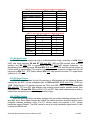
Preface ................................................................................................................ii
READ THIS! .........................................................................................................ii
Warnings .............................................................................................................iii
Safety Suggestions ............................................................................................iv
General Troubleshooting ...................................................................................v
Acknowledgments..............................................................................................vi
Table Of Contents...............................................................................................vii
List Of Figures ....................................................................................................ix
List Of Tables......................................................................................................ix
1.00 General Descriptions..................................................................................1
1.10 QS6............................................................................................................ 1
1.20 QS7............................................................................................................ 3
1.30 QS8............................................................................................................ 3
1.40 QSR ........................................................................................................... 5
2.00 Theory Of Operation...................................................................................7
2.10 Power Supplies .......................................................................................... 7
2.11 QS6/QSR Power Supply ......................................................................... 7
2.12 QS7/QS8 Power Supply .......................................................................... 7
2.12A Transformer PCB ..................................................................................7
2.12B Main PCB..............................................................................................7
2.13 SRAM Battery Backup............................................................................. 7
2.20 Analog Signal Paths................................................................................... 7
2.21 Main Outputs ........................................................................................... 7
2.22 Headphone Outputs ................................................................................ 8
2.23 QS7/QS8/QSR Aux Outputs.................................................................... 8
2.24 Power Up Mute........................................................................................ 8
2.30 Digital Signal Paths.................................................................................... 8
2.31 H8/510 Microprocessor ........................................................................... 8
2.31A RESET..................................................................................................9
2.31B The GAL and Memory Mapped I/O .......................................................10
2.31C Other Processor I/O..............................................................................10
2.31D MIDI......................................................................................................10
2.31E PC Serial Connector .............................................................................11
2.32 The SG ASIC........................................................................................... 11
2.32A Sound Generation .................................................................................11
2.32B ROM Card Connector ...........................................................................12
2.33 The FX ASIC ........................................................................................... 12
2.33A QS7/8/R Digital Optical I/O ...................................................................12
2.34 The KEYSCAN ASIC............................................................................... 12
2.34A Reading Velocity ...................................................................................13
2.34B QS8 Key Construction...........................................................................13
2.40 D-A............................................................................................................. 16
2.41 S6 D-A..................................................................................................... 16
2.42 QS7/QS8/QSR D-A ................................................................................. 17
2.50 PC/MAC Serial I/O ..................................................................................... 17
2.51 QS Serial Input ........................................................................................ 18
2.52 QS Serial Output ..................................................................................... 18
2.53 PC/MAC Switch ....................................................................................... 18
2.53A QS6/7/8 PC Serial.................................................................................19
2.53B QS6/7/8 MAC Serial..............................................................................19
2.53C QSR Variant .........................................................................................19
2.54 H8 UART Clocking .................................................................................. 19
3.00 Test Procedures..........................................................................................20
3.10 Self Tests................................................................................................... 20
3.11 Automated Test Mode ............................................................................. 20
3.12 Individual Test Mode ............................................................................... 20
3.13 Differences In QSR Self Tests ................................................................ 21
Alesis QS Series Keyboards Service Manual V1.00
vii
11/19/06
3.20 Further Testing .......................................................................................... 22
3.21 Testing 48KHz......................................................................................... 22
4.00 Troubleshooting and Repair ......................................................................23
4.10 QS6/QS7/QS8 Disassembly/Reassembly................................................. 23
4.20 QSR Disassembly/Reassembly................................................................. 25
4.30 Replacing A Whole Keyboard.................................................................... 25
4.40 Replacing Individual Keys.......................................................................... 25
4.51 Replacing QS6 And QS7 Keys................................................................ 26
4.52 Replacing QS8 Keys ............................................................................... 26
4.60 General Troubleshooting ........................................................................... 27
5.00 Appendix A Pinout Diagrams.....................................................................28
5.10 SG ASIC.................................................................................................. 28
5.11 FX ASIC .................................................................................................. 28
5.12 KEYSCAN ASIC ...................................................................................... 29
5.13 MICRO CONTROLLER ........................................................................... 29
5.14 SRAM ...................................................................................................... 30
5.15 EPROM ................................................................................................... 30
5.16 SOUND ROM .......................................................................................... 30
5.19 GAL ......................................................................................................... 31
5.20 DAC......................................................................................................... 31
6.00 Appendix A Updates And Corrections ......................................................32
6.10 QS6............................................................................................................ 32
6.11 QS6 Main Revision B .............................................................................. 32
6.12 QS6 Main Revision C .............................................................................. 33
6.13 QS6 Main Revision D .............................................................................. 33
6.14 QS6 Main Revision E .............................................................................. 33
6.15 QS6 Main Revision F .............................................................................. 34
6.20 QS7/8......................................................................................................... 35
6.21 QS7/8 Main Revision B ........................................................................... 35
6.22 QS7/8 Main Revision C ........................................................................... 36
6.23 QS7/8 Main Revision D ........................................................................... 36
6.24 QS7/8 Main Revision E ........................................................................... 37
6.25 QS7/8 Main Revision F ........................................................................... 37
6.25 Changes To QS7/QS8 VCO Circuit (All Main PCB Revisions)................ 38
6.30 QSR ........................................................................................................... 38
7.00 Appendix B Software Histories .................................................................39
7.10 QS6............................................................................................................ 39
7.20 QS7/QS8 ................................................................................................... 40
7.40 QSR ........................................................................................................... 40
8.00 Appendix C Sys-Ex Implementations........................................................42
8.10 S6 Sys-Ex .................................................................................................. 42
8.20 QS7/QS8//QSR Sys-Ex ............................................................................. 67
9.00 Appendix D Service Parts Lists .................................................................68
9.10 QS6 Service Parts List............................................................................... 68
9.20 QS7 Service Parts List............................................................................... 72
9.30 QSR Service Parts List .............................................................................. 76
9.40 QS8 Service Parts List............................................................................... 79
10.00 Appendix E Dictionary Of Selected Terms..............................................83
11.00 INDEX ........................................................................................................85
12.00 Schematics................................................................................................88
Alesis QS Series Keyboards Service Manual V1.00
viii
11/19/06
List Of Figures
Figure 1 - QS6 Simplified Block Diagram......................................................................................2
Figure 2 - QS7/QS8 Simplified Block Diagram..............................................................................4
Figure 3 - QSR Simplified Block Diagram .....................................................................................6
Figure 4 - Keyboard Velocity Reponse ........................................................................................13
Figure 5 - QS8 Key Construction.................................................................................................15
Figure 6 - Alesis Serial Port Pinout..............................................................................................17
Figure 7 - Examples of Switch Self Test Key Press Order..........................................................21
Figure 8 - 48KHz Test .................................................................................................................22
Figure 9 - Keyboard Casetop Removal .......................................................................................23
Figure 10 - S6 Case Screw Locations .........................................................................................24
Figure 11 - QS7QS8 Case Screw Locations ...............................................................................24
Figure 12 - QSR Case Screw Locations......................................................................................25
Figure 13 - QS6 Key Release Location .......................................................................................26
Figure 14 - Key Release Catch Location.....................................................................................26
Figure 15 - SG ASIC Pinout ........................................................................................................28
Figure 16 - FX ASIC Pinout .........................................................................................................28
Figure 17 - Keyscan ASIC Pinout ................................................................................................29
Figure 18 - H8 Processor Pinout .................................................................................................29
Figure 19 - FX SRAM Pinout .......................................................................................................30
Figure 20 - EPROM Pinout..........................................................................................................30
Figure 21- Sound ROM Pinout ....................................................................................................30
Figure 22 - GAL Pinout................................................................................................................31
Figure 23 - DAC Pinout ...............................................................................................................31
List Of Tables
Table 1 - Pin to Pin Connections for 9 Pin PC Serial to QS ........................................................ 17
Table 2 - Pin to Pin Connections for 25 Pin PC Serial to QS ...................................................... 18
Table 3 - Pin to Pin Connections for MAC Serial to QS .............................................................. 18
Table 4 - QS6 Main PCB Revision B Changes ........................................................................... 32
Table 5 - QS6 Main PCB Revision C Changes ........................................................................... 33
Table 6 - QS6 Main PCB Revision D Changes ........................................................................... 33
Table 7 - QS6 Main PCB Revision E Changes ........................................................................... 33
Table 8 - QS6 Main PCB Revision F Changes............................................................................ 34
Table 9 - QS7/8 Main PCB Revision B Changes ........................................................................ 35
Table 10 - QS7/8 Main PCB Revision C Changes ...................................................................... 36
Table 11 - QS7/8 Main PCB Revision D Changes ...................................................................... 36
Table 12 - QS7/8 Main PCB Revision E Changes ...................................................................... 37
Table 13 - QS7/8 Main PCB Revision F Changes....................................................................... 37
Table 14 - Schematic Set ............................................................................................................ 88
Alesis QS Series Keyboards Service Manual V1.00
ix
11/19/06
1.00 General Descriptions
The QS series of 64 voice, keyboard and rack mount digital synthesizers represent the
current state of the art in high end digital synthesizers. It is certainly recommended that
technicians be thoroughly familiar with the operation of the units according to the User’s
Reference Manuals before attempting any repair. As is often the case when machines present
the user with so many options, many “repairs” can be made simply through education in the
correct way to use the product. The software histories in Appendix B of this manual may also
prove to be an excellent aid in troubleshooting User difficulties.
Several of these units utilize the same PCBs. For example, the QS7 and QS8 have
identical main PCBs, and all three keyboards (QS6, QS7, and QS8) use the same keypad
PCB. However, some PCBs may be different between individual units while performing similar
functions. In order to minimize confusion between reference designators for the different unit
types, the following conventions will be used throughout this manual:
➫
➫
➫
➫
➫
QS6 Reference Designators are BOLD (e.g. R6, C9)
QS7 Reference Designators are Italicized (e.g. R6, C9)
QS8 Reference Designators are Underlined (e.g. R6, C9)
QSR Reference Designators are Plain (e.g. R6, C9)
Combinations are allowed (i.e. Italicized and underlined indicate both
QS7 and QS8 references) (e.g. R6, C9)
1.10 QS6
With the release of the original S5 (later updated to S5+ A.K.A. S9) QuadraSynth
keyboard and the S4 (later S4+ or S8), Alesis jumped to the forefront of a field in which it had
no previous experience. Since then, we have learned a great deal about the construction of
keyboards, as well as the needs of keyboard players in general. This inevitably led to the
release of the QS6. Smaller, lighter, and with improved sound quality, the QS6 was an instant
success. Still minor improvements have been made through the lifetime of this which have
resulted in several main PCB revisions. Each revision incorporates previous changes as well
as any new improvements made. These changes are outlined in Appendix A. This manual
references the following schematics and component I.D.s unless otherwise noted:
PCB
Main
Slider
Keypad
Schematic Revision
S6 B
S6 B
QS6/7/8 C
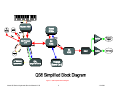
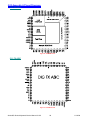
Refer to Figure 1 for a simplified view of the QS6’s electronic systems.
Alesis QS Series Keyboards Service Manual V1.00
1
11/19/06
Figure 1 - QS6 Simplified Block Diagram
Alesis QS Series Keyboards Service Manual V1.00
2
11/19/06
1.20 QS7
The QS7 further expanded and improved the system used in the QS6. The larger QS7
is heavier and therefore less portable, but it’s expanded keyboard enhances it’s use as a
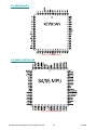
master keyboard controller for the studio. Refer to Figure 2 for a simplified view of the QS7’s
electronic systems. Note that the QS7 is electrically similar to the QS8 (same Main and
Xformer PCBs) and only vary in the number of keys used.
PCB
Main
Slider
Keypad
XFormer
Schematic Revision
QS7/QS8 F
QS7/QS8 A
QS6/7/8 C
QS7/QS8 C
1.30 QS8
In listening to the needs of keyboard players around the world, what came up
consistently was our need to improve the keys themselves. While the weighted keys of
previous units would suffice for most purposes, many high end players still preferred the “feel”
of real piano keys. In answer to this need, Alesis designed the QS8 88 key, piano weighted
keyboard. The keys were specifically designed to simulate the same “feel” that acoustic piano
keys have when the hammer strikes the piano strings. Incorporating the same basic sound
engine as it’s predecessors, the QS8 is sure to rank highly among players and composers
alike. (Minor improvements have be made through the lifetime of this product. This has
resulted in several main PCB revisions. Each revision incorporates previous changes as well
as any new improvements made. These changes are outlined in Appendix A. This manual
references the following schematics and component I.D.s unless otherwise noted: Refer to
Figure 2 for a simplified view of the QS8’s electronic systems.)
PCB
Main
Slider
Keypad
XFormer
Alesis QS Series Keyboards Service Manual V1.00
Schematic Revision
QS7/QS8 F
QS7/QS8 A
QS6/7/8 C
QS7/QS8 C
3
11/19/06
Figure 2 - QS7/QS8 Simplified Block Diagram
Alesis QS Series Keyboards Service Manual V1.00
4
11/19/06
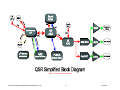
1.40 QSR
Many current keyboard players already have their favorite controller keyboard, but still
desire the great sound provided by the Alesis QS Series. Since multiple keyboards can take up
excessive space, the obvious solution is a rack mount sound engine without keys. The QSR is
just that solution. Whether used for the road or in the studio, the QSR is a powerful addition to
any MIDI setup. Minor improvements have been made through the pre production lifetime of
this product. This has resulted in several main PCB revisions. Each one incorporates previous
changes as well as any new improvements made. These changes are outlined in Appendix A.
This manual references the following schematics and component I.D.s unless otherwise noted:
PCB
Main
Front Panel
Alesis QS Series Keyboards Service Manual V1.00
Schematic Revision
A
X2
5
11/19/06
Figure 3 - QSR Simplified Block Diagram
Alesis QS Series Keyboards Service Manual V1.00
6
11/19/06
2.00 Theory Of Operation
2.10 Power Supplies
2.11 QS6/QSR Power Supply
The power supply begins with the Alesis P4 type transformer input at J1 J15. After the
power switch (SW2 S1), the signal is rectified (D1, D2 D12 D11), input filtered (C3, C9 and C25
C86, C80 and C81), regulated (U9, U10 U31, U32), and finally output filtered (C24, C32 and
C35, C34 C77, C78 and C82, C83) into the +5V and -5V supplies needed by the unit. In
addition, many 0.1µF capacitors are located throughout the system to act as supply filters. Note
that the +5V rail requires a lot more filtering due to the digital supply needs.
2.12 QS7/QS8 Power Supply
2.12A Transformer PCB
Input from R.F.I. filter enters the Transformer PCB via J1. The current is fused (F1)
prior to the primary of the ECO 4 Transformer (X1). Note that the transformers of countries
outside the United States are varied according to the power grid requirements for that country.
Output from the transformer PCB is routed to the main PCB via J2.
2.12B Main PCB
Transformer output is bridge rectified (D1, D2, D4 , and D5), input filtered (C8, C96, and
C15), regulated (U6, U4), and finally output filtered (C38, C34, C18, and C24) into the +5V and
-5V supplies needed by the unit. In addition, many 0.1µF capacitors are located throughout the
system to act as supply filters. Note that the +5V rail requires a lot more filtering due to the
digital supply needs.
2.13 SRAM Battery Backup
The user storage/system SRAM requires a small standby supply current while it is
normally powered down. The battery current is supplied via a transistor circuit (Q7 Q4 Q4)
designed prevent the +5V rail from trying to charge the battery, while ensuring that a solid +5V
is supplied to the SRAM during normal operation.
2.20 Analog Signal Paths
Since these units are largely digital in nature, analog signals are limited to two major
types:
☞
☞
Audio Signal Output
Slider and Aftertouch strain gauge input
2.21 Main Outputs
Differential analog output from the DAC is anti-alias filtered and buffered by U6A U3A
U3A (left) and U6B U3B U3B (Right). This signal is sent to the stereo output level slidepot R1
R2 via J11 J4 J1.
Alesis QS Series Keyboards Service Manual V1.00
7
11/19/06
2.22 Headphone Outputs
The signal from the volume slider is sent through a X10 X3 X3 gain stage U5A, U5B
U2A, U2B U1B, U1A, current limited R12, R13 R3, R2 R1, R2 and output through the stereo
jack J2 J1 J1.
2.23 QS7/QS8/QSR Aux Outputs
The Aux outputs are completely isolated from the main outputs by virtue of a separate
DAC U3 U4. The differential output of the DAC is anti-alias filtered and buffered by U3C U3C
(left) and U3D U3D (right). This signal is current limited (R31, R32 R31, R32), R.F. Filtered
(C35, C36 C33, C34), and output via the ¼ “ jacks (J8, J9 J5, J4).
2.24 Power Up Mute
The Power Up (PUP) mute circuit ensures that no sound is output during the critical
stages of powering the unit up and down. Most often noise is created due to the uneven power
demands placed on the positive and negative rails, especially at power up. There also may be
noise due to the random power up states in the digital hardware prior to the software
establishing correct values. Muting is accomplished with the use of the microprocessor reset
line (See Section 2.31A).
The positive and negative supplies are fed to the final analog output stages via
transistors Q2, Q4 Q1,Q3 Q1, Q3. R48, R50 and R51 R13, R18 and R19 R13, R18 and R19
are used to bias these transistors into saturation when the circuit is switched on. Q3 Q2 Q2
provides the necessary current to switch the supply transistors on, as well as providing a
threshold value for timing purposes. Since power up noise may extend past the time necessary
for the digital hardware to physically reset, a further time delay is required before the output is
allowed to turn on. This is accomplished with an RC circuit comprised of R49 and C30 R20 and
C14 R21 and C13. D15 D3 D1 provides a quick discharge path for the capacitor so that the
circuit functions correctly even if power is cycled off and on rapidly.
Note that in the QS6 it was found that this circuit did not load down the RST line (see
Section 2.24), causing power up reset to take longer than it should. The extra inverter was
eliminated in the QS7/QS8/QSR.
2.30 Digital Signal Paths
2.31 H8/510 Microprocessor
The H8 Microprocessor (U16 U21 U20) is the primary device in control of all information
flow in the QS Series. At the appropriate times, the H8 accepts input from various sources
(Keyboard, MIDI, etc.) and determines the correct response (play sound, output data to MIDI,
etc.). All of this information flow is under the direct control of the software stored in the
EPROM (U19, U18, U17).
Although a complete discussion of H8 programming is beyond the scope of this manual,
it is appropriate at this time to state the importance of understanding overall unit operation
including the interactions between hardware and software. Not only is it possible to
troubleshoot usage errors (i.e. keyboard not loading DataDisk files because Sys-Ex is
disabled), it can also make troubleshooting hardware easier as well. For example: it is easier
to troubleshoot a MIDI output problem by sending longer files out through MIDI while examining
the MIDI output circuit with an oscilloscope. The longer the file, the more time there is to look at
the circuit before having to send the file again. While this is a relatively simple example, it
Alesis QS Series Keyboards Service Manual V1.00
8
11/19/06
shows that knowing how the hardware is supposed to respond to software changes can greatly
simplify the task of hardware troubleshooting.
The most important pins are:
➠
➠
➠
➠
➠
➠
➠
D0-D16
16 Bit Data Buss (note that in the QS Series some of the other
devices only use 8 bits of the data buss. This may cause some
noise in the unused data lines during processor reads making
the appear “bad” due to a floating input. While ignored by the
software, it can make troubleshooting a real open in the data
buss more difficult.
A0-A23
23 Bit Address Buss (Note that only 20 bits are actually used).
RES
System RESET line. Asserted only during power up/down. (See
Section 2.31A)
RD
Read Enable
HWR
Write Enable
XTAL, EXTAL Input for system clock crystal.
PX.X
I/O Ports are configured by the software and allow the software
some direct hardware access. In particular are:
➱
➱
➱
➱
➱
➱
➱
➱
➱
➱
➱
➱
➱
➱
➱
TXD1
Transmit Serial Data line to MIDI output circuit (See Section 2.31D).
TXD2
Transmit Serial Data line to PC/MAC output circuit (See Section 2.50).
RXD1
Receive Serial Data line From MIDI In circuit (See Section 2.31D).
RXD2
Receive Serial Data line From PC/MAC input circuit (See Section 2.50).
PITCH
Pitch Wheel data input (See Section 2.31C).
DATA
Data Slider data input (See Section 2.31C).
MOD
Mod Wheel data input (See Section 2.31C).
RES
CD1
PCMCIA Card #1 Present Switch input (See Section 2.32B).
CD2
PCMCIA Card #2 Present Switch input (See Section 2.32B).
PC/MAC PC/MAC Serial Port Switch input (See Section 2.50).
KEYINT Keyscan ASIC interrupt .input (See Section 2.33).
SUS
Sustain Pedal Input.
SMUTE
DAC Output Mute
EDIT PCB SWITCH MATRIX (See Section 2.31C).
2.31A RESET
Reset is one of the single most important circuits/signals in the entire unit. Without a
correct RST signal during power up and power down, any number of problems can occur.
These can range from an occasional failure such as an odd audio “blip”, to complete, system
wide lock ups and data corruption. Therefore any time processor problems are suspected, RST
should be the first thing checked.
In order to ensure that data will not be corrupted, the reset circuit uses the raw power
supply signal to determine the correct time to assert the RST signal (i.e. not until the regulated
+5V supply rail contains no ripple). This is done by using a raw supply threshold of
approximately 7V. Since the power down sequence of events is generally the reverse of the
power up process, only the power up events are described here.
Alesis QS Series Keyboards Service Manual V1.00
9
11/19/06
It helps to know the initial state of the active devices in the circuit. While the raw supply
is just below the raw supply threshold Q5 Q5 Q5 is turned off, allowing the base of Q6 Q6 Q6
to be pulled high via R40 R38 R62 , turning it on. This in turn holds the voltage across C15
C42 C59 at 0.7V (approximately ground). These in turn keeps the input to the first inverter
U7A U9C U19A low. Thus RST is high and RST is low. In addition, the S6 incorporates an
extra inverter (U7E) to drive the power up mute circuit (see Section 2.24).
The process begins when the raw +5V supply reaches the reset threshold. The voltage
divider consisting of R52, R39 and D6 R36, R37 and D9 R60, R61 and D10 scales the level of
the raw supply so that Q5 Q5 Q5 turns on at the preset threshold. This pulls the base of Q6
Q6 Q6 to 0.7V (low) turning it off. This allows the voltage across C15 C42 C59 to charge
slowly via R41 R39 R63 (this also adds a time delay that prevents raw supply ripple from
triggering multiple resets). Once this voltage rises above the threshold level of the Schmidt
Trigger inverter it switches states, pulling RST low and RST high, completing the reset cycle.
2.31B The GAL and Memory Mapped I/O
While the H8 has been optimized as a controller device, it is none the less somewhat
limited in the number of direct input and output lines available. Memory mapping is the simplest
method of allowing software designers the ability to manipulate the large number of hardware
registers directly from the microprocessor with a minimum of external hardware.
The idea is to “fool” the microprocessor into thinking that hardware register locations
(latches) are actually memory locations. The process begins when the H8 sets up the address
buss. The GAL (U12 U13 U9) checks this address to see if it is in the range of hardware
registers. If the H8 address is within the confines of normal memory, the RAM or ROM signal is
asserted and memory is accessed normally. However if the address is in the hardware range,
the GAL decodes the address and strobes the chip select line of the appropriate device. Each
device must interpret the state of the microprocessor ReaD and WRite lines and send or
receive data appropriately. It is left up to the software to “know” which devices are written to as
opposed to read from.
2.31C Other Processor I/O
All other “outside world” communication of the processor not handled via memory
mapped I/O (See Previous Section) is sent and received via the H8’s built in I/O ports. These
are automatically configured by the software at power up. These lines all have internal pullup
resistors. These “outside world” devices include pedals, front panel key switches. and pitch,
mod, and data wheel inputs.
2.31D MIDI
MIDI input is opto isolated (U4 U7 U14) from the MIDI Input Jack (J7 J12 J8). R2 R35
R49 current limits the incoming signal while D3 D7 D6 serves to protect the opto isolator from
reverse bias currents. R42 R40 R51 serves to set the internal threshold level of the opto
isolator while R22 R41 R50 augments the internal pullup of the H8’s input port.
MIDI output is initiated from the H8’s output port. Two elements of a Schmidt Trigger
inverter (U7C and U7D U9B and U9E U19E and U19B) are used to buffer the outgoing signal.
This signal is current limited (R1 R45 R53) before being sent to the MIDI Output Jack (J8 J13
J9).
In addition, the QS7, QS8, and QSR incorporate a similarly designed MIDI THRU (U9A
and U9F U19C and U19D, R45 R55, J14 J10).
Alesis QS Series Keyboards Service Manual V1.00
10
11/19/06
For further information about MIDI, consult MIDI SPEC available from the International
MIDI Association.
2.31E PC Serial Connector
While technically a part of standard H8 I/O, Computer Serial I/O is complex enough to
warrant it’s own section (See Section 2.50).
2.32 The SG ASIC
In order for the unit to play a sound sample, the H8 µP (See Section 2.31B) must
receive a command via the keyboard (via the Keyscan ASIC) or through MIDI. The
Microprocessor then tells the SG ASIC three things:
1. The note value (e.g., C3, D#4, A6, ...).
2. The velocity of the note value.
3. The type of sound to be played (dependent on PROGRAM, MIX, MIDI Channel, etc.).
The SG ASIC then retrieves the correct 16-bit sound information from the SOUND ROM
according to the instructions sent by the H8. In addition, the SG ASIC performs the duties
necessary to create the envelope of the voice (e.g., Attack, Decay, Sustain and Release) as
well as other audio functions such as changing filters.
SG ASIC instructions are passed to it by the H8 µP through memory mapped I/O (See
Section 2.31B).
There is one clock signal for the SG ASIC. It is received at pin 19. The clock is
generated from crystal M2 via U18A. The clock signal is also frequency halved , and output via
pin 12. This 12.288MHz clock is used in the QS6 by the 74HC390 (U17) {to derive other
system clock signals (1MHz, 614.4MHz)}. System signals in the QS7, QS8 and QSR are
derived slightly differently providing for better software control (See Section 2.54). Note also
that the QS7, QS8 and QSR all utilize a digital VCO (U11 U7) to provide extremely stable
clocks to the sound generation system.
The SG ASIC can send sound information to the FX ASIC by two possible ways. The
first is the 8 bit data buss. The second is via optical information from EOPTOUT (pin 3), to the
FX ASIC. Currently, the optical buss is used for all communication.
2.32A Sound Generation
Sound is generated with the use of Sample ROM playback. The playback is
accomplished by the SG ASIC while the sounds themselves are contained either in the MASK
ROMs (2 Megabytes each) or in a PCMCIA CARD attached to the system. As far as sound
generation is concerned, the only distinguishable difference between the two is their relative
location in the SG ASIC’s memory map, and as such will be referred to simply as Sound ROM.
Besides actual sonic data, Sound ROM also contains data about the samples Start, End, and
Loop points, start and end volumes, sample rate, and data smoothing coefficients.
When the H8 receives a command to play a sample (keyboard, MIDI, or PC Serial) it
notifies the SG ASIC what note value and velocity have been requested. The SG ASIC then
retrieves data for 2 samples. The first sample is the requested sample. The second is the
sample at the next higher address. This is necessary because current technology does not
allow for a sample to be taken at possible note value (the amount of necessary memory jumps
prohibitively when this is attempted). Instead, a number of “key” samples are provided and the
SG ASIC’s DSP is called upon to interpolate for the correct note pitch value. The notes that
each individual sample is responsible for is called a “Keygroup”. Note that the pitch
interpolation also takes into account any variations in pitch that may occur due to modulation
(i.e. pitch wheel or LFO Modulation).
Alesis QS Series Keyboards Service Manual V1.00
11
11/19/06
Once pitch scaling is done, the SG ASIC similarly scales the amplitude of the data.
Again it must take into account such things as the sample’s natural envelope, the
Attack/Decay/Sustain/Release envelope provided for in the patch by the user, and any other
modulations necessary.
The “massaged” data is now ready to be passed along to the FX ASIC for further
processing and output. (See Sections 2.33, 2.40, and 2.20)
2.32B ROM Card Connector
Since Sound Cards serve the same function as the Sound ROMs, they are also
generically referred to as “Sound ROM”. The description of how the SG ASIC generates sound
from this is equally valid for both (see Section 2.32A). However, several extra lines exist to help
the H8 processor distinguish between Sound Cards and Sound ROM. This is especially
important as the H8 must be able write to the Sound card as well as read from it. CD1 and CD2
are used to inform the H8 of the presence and type of Sound Card inserted into the unit. In
addition, because the unit must be able to write to the Sound Card (as opposed to Sound ROM
which is read only) ReaD and WRite from the H8 are passed along via the SG ASIC SOE
SWR.. Since the QS7, QS8 and QSR have 2 ROM card slots all chip enable and card enable
lines must be duplicated (i.e. CE1, CE2).
2.33 The FX ASIC
The FX ASIC is one of Alesis’s custom digital signal processing ICs. Capable of up to 4
effects at once, this device is essentially a rack mount effects unit in a chip. The only other
essential major parts are memory for storing samples currently being manipulated, instructions
on what to do with the sound, and of course the sound data itself.
In the QS Series the Buffer DRAM is in the form of an HM514260AJ-7, a 4 Megabyte
70nS access part arranged as 16 bits X 256K words, for a maximum of approximately 5
seconds of sample time. This gives the FX ASIC plenty of room to create the convincingly
realistic sonic effects Alesis is famous for. The main control signals for the FX DRAM are RAS
(Row Address Strobe), CAS (Column Address Strobe), and WRN (WRite eNable). The 16 bit
data and 9 bit address busses operate the same as any standard micro processor.
Algorithm instructions are passed to the FX ASIC’s Writeable Control Store by the H8
processor via the memory mapped I/O process (See Section 2.31B).
In addition the FX ASIC is the last purely digital IC in the signal flow so the FX ASIC is
also responsible for DAC and Optical output (See Section 2.40).
2.33A QS7/8/R Digital Optical I/O
While the SG ASIC is capable of handling Optical I/O directly, all outside (via the optical
output jack J10 J8) communication is directed by the FX ASIC. In addition, the optical buss is
used internally to transfer data serially from the SG ASIC to the FX ASIC via the OPT_IN line
(pin 20). Output from EOPT_OUT (pin 19) is sent directly to the optical output jack.
2.34 The KEYSCAN ASIC
While the task of polling the keyboard may seem difficult at first (up to 88 Keys with
velocity), the Keyscan ASIC takes care of this task and passes the information back to the H8
processor . The main signals of the Keyscan ASIC are:
Alesis QS Series Keyboards Service Manual V1.00
12
11/19/06
➫ DD0-DD7
➫
➫
➫
➫
➫
➫
➫
➫
➫
➫
A0
RD
WR
KEY
KEYINT
KEYCLK
ROW0-7
COL0-21
VSS1-4
VDD1-4
Data Buss bits 0 to 7. Correspond to the upper 8 data bits of
the H8.
H8 Address Buss bit 0
H8 ReaD enable
H8 WRite enable
Chip select line from GAL (Mapped I/O)
Output to H8 interrupt line
Clock input from H8
Row input from keyboard switch matrix
Column input from keyboard switch matrix
Source Supply (GND)
Drain Supply (+5V)
2.34A Reading Velocity
Velocity response is measured through the time differential between two switch closures
and works like this:
➠ The harder a key is pressed, the
faster it moves.
➠ Since Rate = Distance/Time
knowing the time it takes to move
the key through a specific distance
tells us how fast it’s moving and
thus the force acting on it.
➠ This is accomplished by using 2
switch
contacts
mounted
at
different distances from each other.
The rubber in the keypad acts as a
spring,
both
absorbing
the
compression of switch 1, as well as
pushing the carbon contacts away
from the PCB contact points when
the key is release.
➠ The Keyscan ASIC counts up the
time it takes between switch 1
closing and switch 2 closing. Since
distance (between the switches) is
preset in the design, time difference
is taken as a direct measure of
velocity.
2.34B QS8 Key Construction
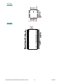
Figure 4 - Keyboard Velocity Reponse
All keyboards in the QS Series function
identically in an electrical sense. However, since the QS8 keyboard is different in mechanical
construction from the rest of the line, a word or two about it is appropriate at this point. In order
the simulate the action of a true piano keyboard the FATAR TP/20 keyboard uses moving
metal weights striking a felt strip to emulate the action of the piano’s hammer striking a string.
Figure 5 shows the basic setup of the keys. Note the “action” of the two “levers” involved
in the process. The first lever which is the key itself is single ended, with it’s fulcrum located at
the “back” end of the key. The second lever is the double ended counterweight. With it’s
Alesis QS Series Keyboards Service Manual V1.00
13
11/19/06
fulcrum offset from center to increase the relative momentum of the weight, it is pushed on one
end by the motion of the key. The other end of the counterweight is free to move until it strikes
the felt strip attached to the frame (i.e. the hammer hits the string).
The individual keys are isolated from the frame by a plastic clip. Individual broken keys
are easily replaced by releasing the clip as shown in Figure 14.
Since the counterweight alone is not enough to force the key up again, a spring located
near the key fulcrum is used to push the key back into place.
Alesis QS Series Keyboards Service Manual V1.00
14
11/19/06
Figure 5 - QS8 Key Construction
Alesis QS Series Keyboards Service Manual V1.00
15
11/19/06
2.40 D-A
The D-A sections of the QS Series vary slightly from unit to unit. These variations are
minor so the circuits are relatively similar, especially on the digital side of the IC. Most of the
analog differences depend on the D-A Device used. Both devices are made by AKM and come
from the same “family” (43XX Series). The main differences between the two are in the power
supply filtering required by these two devices. There are also internal differences resulting in
slightly better noise characteristics for the 4319.
As Aux Outputs are functionally identical the unit’s main outputs, only the mains will be
discussed here.
2.41 S6 D-A
The S6 Digital-to-Analog Converter is an AKM4318A (U3). A bit clock (BICK) of 3.072
MHz, buffered by an inverter (U18B), is sent from the FX ASIC (U11). This clock signal is sent
to pin 13 of the DAC which is used to latch the serial data on SDATA (pin 14) into the device.
The LRCK (pin 12) input is the left and right channel clock. This 48KHz clock signal is
originated from the FX ASIC at pin 11. SMUTE mutes the analog outputs and is controlled by
the H8 processor (pin 53).
The analog supply (+5V) is filtered by C28 and C29. The digital supply is provided via
D4 and D5 (for approximately a 1.4V drop) from the +5V supply and filtered by C22 and C21.
The DAC outputs are balanced and are routed through differential amplifiers to the unit's
output jacks, via the analog output circuitry (See Section 2.20).
Alesis QS Series Keyboards Service Manual V1.00
16
11/19/06
2.42 QS7/QS8/QSR D-A
The QS7/8/R Digital-to-Analog Converter is an AKM4319 (U3 U2). A bit clock (BICK) of
3.072 MHz, buffered by a NAND gate acting as an inverter (U12D U10D), is sent from the FX
ASIC (U10 U6). This clock signal is sent to pin 5 of the DAC which is used to latch the serial
data on SDATA (pin 6) into the device. The LRCK (pin 4) input is the left and right channel
clock. This 48KHz clock signal is originated from the FX ASIC at pin 11. SMUTE mutes the
analog outputs and is controlled by the H8 processor (pin 53).
The analog supply (+5V) is filtered by C3 C3 and C7 C8. The digital supply is also
provided from the +5V supply and filtered by C6 C26.
In addition the QS7/8/R use an AUX DAC (U5 U4) for the Aux Output which functions
identically to the Main output.
The DAC outputs are balanced and are routed through differential amplifiers to the unit's
output jacks, via the analog output circuitry (See Section 2.20).
2.50 PC/MAC Serial I/O
As with MIDI, this connector is a serial device with the
majority of the work being expedited by the software running in
the H8. Since there are two basic types of computer in general
use, a great deal of extra hardware is required. As much as
possible, the Alesis design team engineered the circuitry to
reduce the parts count, and combine as much of the two
different types as possible. The IBM compatible PC uses a single
ended serial buss while the Macintosh version uses a balanced
line signal for transmission and reception. In addition, the two
different types require different handshake and BAUD rate clock
circuitry. Figure 6 shows the pinout of the Alesis QS serial port
and Tables 1-3 show the pin to pin connections of the various Figure 6 - Alesis Serial Port Pinout
Alesis Serial Cables 1, 2, and 3.
Note that the QS6 is hardware limited to a BAUD rate of 38.4 KHz. All subsequent
designs use software controlled frequency division to achieve a variable baud rate (See
Section 2.54).
Table 1 - Pin to Pin Connections for 9 Pin PC Serial to QS
Purpose
HSKO (Enable 4-12V)
Return (Enable Return)
TXD
GND
RXD
NC
NC
NC
Alesis QS Series Keyboards Service Manual V1.00
QS Serial Pin
1
2
3
4
5
6
7
8
17
PC Pin
8
7
2
5
3
NC
NC
NC
11/19/06
Table 2 - Pin to Pin Connections for 25 Pin PC Serial to QS
Purpose
HSKO (Enable 4-12V)
Return (Enable Return)
TXD
GND
RXD
NC
NC
NC
QS Serial Pin
1
2
3
4
5
6
7
8
PC Pin
5
4
3
7
2
NC
NC
NC
Table 3 - Pin to Pin Connections for MAC Serial to QS
Purpose
1MHz
NC
TXD GND
RXDTXD+
GPI (NC)
RXD+
QS Serial Pin
1
2
3
4
5
6
7
8
MAC Pin
2
1
5
4
3
8
7
6
2.51 QS Serial Input
PC/MAC input is passed through a buffer/translation stage consisting of U2A U31C
U24C and some resistors. R8 and R7 R96 and R97 R85 and R86 provide some resistive
isolation and R8 R96 R82 in combination with R27 R94 R83 provide hysteresis for
waveshaping the incoming signal. R9 and R10 R95 and R93 R83 and R84 act as pullups to
further assist in waveshaping. The output of the comparator is resistively isolated from the H8
input port by R28 R87 R74. Pullup resistor R30 R41 R50 ensure the correct TTL signal levels
(pulled up to +5V).
2.52 QS Serial Output
PC/MAC output initiated by the H8 processor is differentiated into the balanced signals
required by the MAC via the comparator pair of U2D and U2C U31B and U31A U24A and
U24B. (Note that the PC interface ignores the TXD- and RXD- lines.) Pullups R26 and R25
R96 and R81 R73 and R67 help maintain the outgoing signal despite possible losses from
long cable runs. R6 and R24 R85 and R80 R72 and R71 help match impedances as well as
current limit and resistively isolate the signal before output.
2.53 PC/MAC Switch
Note the seemingly minor hardware changes that occur when switching between the PC
and MAC lines. Since these changes are critical this switch should be checked carefully when
computer interface problems occur. The PC version sends and receives a D.C. voltage
handshake signal (Enable). The MAC needs to see a bit clock handshake signal which it uses
to determine BAUD rate.
Alesis QS Series Keyboards Service Manual V1.00
18
11/19/06
2.53A QS6/7/8 PC Serial
In these units the Enable handshake signal is provided by simply closing the loop
provided by the host computer (Enable Return) via the DPDT PC/MAC switch (SW1 SW1). The
switch also is used to inform the H8 that the PC type is currently in use and should adjust the
software and/or hardware accordingly. The BAUD rate is determined by the FREQ input to the
H8 (See Section 2.54). In the QS6, handshake hardware is fixed at 614.4KHz, so no
adjustment can be made by the H8, hence it’s BAUD rate limitations.
2.53B QS6/7/8 MAC Serial
In the MAC interface, BAUD rate information must be passed along to the host
computer along with the data itself. This is provided via comparator U2B U31D U24D (used
here as a line driver). In the MAC position, SW1 sends the bit clock out through pin 1 of the QS
Serial port. The switch also is used to inform the H8 that the MAC type is currently in use and
should adjust the software and/or hardware BAUD rate accordingly. The bit clock signal is also
needed by the FREQ input to the H8 (See Section 2.54). In the QS6, handshake hardware is
fixed at 614.4KHz,so no adjustment can be made by the H8, hence it’s BAUD rate limitations.
2.53C QSR Variant
Note that the QSR varies slightly in that it’s PC/MAC switch is a software function rather
than a physical switch. Q7 is used here provide the necessary switching action to correctly bias
the handshake signal driver U24D.
2.54 H8 UART Clocking
There are 2 internal UARTs (Universal Asynchronous Receiver Transmitter) in the H8 (1
for MIDI and 1 for computer serial I/O). It should be noted here that the MIDI UARTs all operate
at the same fixed rate so further discussion of UART clocking will be limited here to the UART
used for computer serial I/O.
In order for serial data to be transmitted and received at the correct speed, the UART
must be clocked at the correct speed via the FREQ input (pin 92). In the QS6 it is simply
derived from the system clock via U17 and U20A limiting it’s BAUD rate. In later models
however, the BAUD rate is variable to match the speed of the host computer, so a little extra
hardware is needed. U26 U27 is used as a software controlled variable frequency divider.
Control input to the 74HC161 is provided by the H8 in the form of a “count” value. The Carry
output is used to force the device to load the new “count” input via U25A U26A. The Carry
output is also passed along to a divide by 2 waveshaping flip-flop (U29A U29A) before being
sent to the H8 FREQ input. There are also 2 clock sources available (again selectable by the
H8 via gate logic comprised of U28 and U25C U28 and U26C). The first is the 20MHz system
clock (M2 M2), and the second is a 14MHz clock (M3 M3) intended strictly for this purpose.
The ultimate purpose of all of this is to determine how fast the H8’s TXD and RXD lines send
and receive data.
Alesis QS Series Keyboards Service Manual V1.00
19
11/19/06
3.00 Test Procedures
If at all possible, user memory should always be saved (PCMCIA Card or MIDI SYS-EX)
prior to service. It’s also important to remember that user data itself may be corrupted for a
variety of reasons. So if for some reason a unit continues to “crash” when reloaded, it’s not
unreasonable to expect bad data to be the cause.
3.10 Self Tests
The QS Series Software is specifically designed to assist in troubleshooting hardware
problems. This assistance comes in the form of a series of self test routines that check various
aspects of the hardware. There are two different methods of accessing these routines. One is
an automated run through all tests, while the other allows the choice of which individual tests
are run. Note that due to the extreme difference in the QSR’s front panel, the self tests
themselves and the method they are accessed are also different. See Section 3.13 for a
thorough discussion of the QSR Self Tests.
✔ Pressing “0” and “03” during Power up reinitializes all software values to their ROM presets.
✔ Pressing “0” and “10” during power up initiates the Automated Self Test Mode.
✔ Pressing “0” and “00” during power up establishes Individual Test Mode.
3.11 Automated Test Mode
Before initiating the automated self Test Mode it is necessary to plug in all necessary
cables (MIDI IN to MIDI OUT, PC Serial Test Cable). If this is not done the test will fail when
the missing cable is encountered. Pressing the Value ↑ button will skip the failed test and
proceed to the next. (See the next section for a full description of each test)
3.12 Individual Test Mode
When in Individual Self Test Mode, the Value ↑ and Value ↓ are used to select which
test is to be run and pressing “STORE” will select it. All tests stop upon completion of the test
(display shows “TEST PASSSED” or “TEST FAILED”). Pressing Value ↑ or Value ↓ will exit the
test and return to the Individual Test Menu. The tests are:
1. TEST EPROM - This routine does a Checksum test of the Software EPROM. This test ends
with either a pass or fail. A failure probably indicates a faulty EPROM, but may also indicate
a problem with the H8 itself, or in fact any of the other device attached to the data and
address busses, or the busses themselves (i.e. broken address trace).
2. TEST SRAM - This routine performs a functionality test of the H8’s Storage memory. As
with the EPROM test above, a failure here probably indicates a truly faulty SRAM, however
a persistent failure (one that occurs after the SRAM has been replaced) may be in fact due
to errors in the H8’s subsystems.
3. TEST MIDI I/O - A MIDI Cable must be connected between MIDI IN and MIDI OUT prior to
starting this test. It will the send and receive a data stream to ensure functionality of both IN
and OUT. Note that due to the fact that the MIDI Input and Output circuits are internally
grounded (through the PCB traces), this test can not detect a broken ground on either jack
(i.e. poor solder or broken jack pin).
4. TEST PC I/O - Prior to initiating this test pins 3 and 5 must be shorted together (this can be
done with a paperclip, although a cable expressly made for this purpose is preferred) and
the PC/MAC switch set to the PC position. Since there are so few components in this
Alesis QS Series Keyboards Service Manual V1.00
20
11/19/06
5.
6.
7.
8.
circuit, failures should be relatively easy to troubleshoot although failures with the BUAD
rate circuitry can also affect serial operation.
TEST F/X DRAM - This routine forces the F/X ASIC to write to and read from every location
in the F/X DRAM. This will take about 40 seconds. As with the EPROM test above, a failure
here probably indicates a truly faulty DRAM, however a persistent failure (one that occurs
after the DRAM has been replaced) may be in fact due to errors in the F/X ASIC’s
subsystems.
TEST SOUND ROM - Like the EPROM Test above, this routine does a checksum of each
of the QS’s Sound ROMs. Again the associated address or data buss failures may appear
as a legitimate Sound ROM failures.
TEST SWITCHES - After initiating this test, each front panel button must be pressed in the
correct sequence. This ensures that each button is not only functional, but it also checks for
key debounce errors (i.e. the
unit “sees” the key pressed
several times even though it
was only pressed once). The
sequence
starts
at
the
rearmost left hand button
continues forward, then to the
right (See Figure 7 for an
Figure 7 - Examples of Switch Self Test Key Press Order
example).
TEST POTS - This test allows the technician to verify the function of the mod and pitch
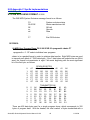
wheels, as well Data pots or sliders. Once initiated, the LCD will show several numbers.
Each of these numbers represents the position of one of the pots. Data Pots will normally
show a range of 0 - 1023. Pitch and Mod wheels have a range of 0 - 600 and the Aftertouch
has a range of 0 - 300. Moving each pot will cause the corresponding number in the display
to change.
3.13 Differences In QSR Self Tests
Because it is a rack mount unit and it’s buttons are different from the keyboard versions,
the self test routines for the QSR are slightly different. The manual self test (there is no
automated version) is initiated by holding MIDI CH ← and →. Use Cursor ← or → to select the
test to run. Pressing STORE initiates the test. Pressing either cursor button exits the test. Note
that pressing Cursor ← and → shows the current software version, but only if the unit is in MIX
or PROGRAM Play modes (i.e. the unit is not in EDIT or SELF TEST). The tests are:
0.
1.
2.
3.
4.
5.
6.
7.
Test EPROM - Same as the keyboard test.
Test SRAM - Same as the keyboard test.
Test MIDI I/O - Same as the keyboard test.
Test PC I/O - Same as the keyboard test.
Test F/X DRAM - Same as the keyboard test.
Test Sound ROM - Same as the keyboard test.
Test Switches - Same as the keyboard test.
Test Encoder/LED - Once initiated, front panel LEDs (under the buttons) will cycle
according to the direction the data wheel is turned. Press STORE to exit this test.
8. Test Display - This test simply turns on all of the display elements in the LCD.
9. Test Audio - This test simply sends audio through all outputs. This is extremely useful when
troubleshooting analog circuit problems.
Alesis QS Series Keyboards Service Manual V1.00
21
11/19/06
3.20 Further Testing
Naturally it is a good idea to actually play the keyboard. Be sure to check that pitch and
velocity scaling sound normal. It’s also important to check the Aftertouch to ensure it’s function.
Note that in the QS8 it is important to check the Aftertouch of white and black keys separately
as each of these key sets has it’s own Aftertouch cable.
While the self test will pick up most circuit errors, MIDI should still be tested in both send
and receive. This can be done 3 ways:
➪ Record and playback from a MIDI Sequencer
➪ Save and load Sys-ex data from a MIDI Librarian or DataDisk.
➪ Use a second keyboard to send trigger notes to the unit under test.
Also test that key presses from the unit under test trigger notes on
the other keyboard or an extra module.
If at all possible, the PC/MAC Serial connector should be tested similarly, as well as all
other I/O type circuitry such as 48KHz, PCMCIA, and optical (with the use of an ADAT
Multitrack).
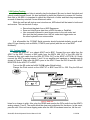
3.21 Testing 48KHz
Obtain an ADAT-XT or a classic ADAT and a BRC. Connect the sync cable from the
ADAT to the BRC. Connect a BNC cable from the BRC's 48K OUT to the QS's 48K IN.
Connect a fiber optic cable from the QS's OPTICAL OUT to the ADAT's OPTICAL IN. Finally
connect the ADAT's analog outputs 1 and 2 to an amplifier and speakers or headphones as
shown in Figure 8. Make sure the BRC syncs to the ADAT. Press the DIG IN and ALL INPUT
MONITOR on the ADAT-XT or BRC.
Turn on the QS under test's 48K IN ON (under Global button).
Change the Pitch control on the ADAT-XT or BRC from 000 to -300. Play the QS and
Figure 8 - 48KHz Test
listen for a change in pitch. Also, play the DEMO and monitor the QS's audio from the ADAT's
analog outputs 1 and 2. The audio should be clean and undistorted for the above. In this event,
pass the unit. If the unit has a clipping noise after the 48K IN has been turned on, fail the unit.
Alesis QS Series Keyboards Service Manual V1.00
22
11/19/06
Note: If the QS's power is turned off, the 48K IN must be turned on again. The display
may show that the 48K IN is on, but it MUST be toggled back to ON to get it to work
4.00 Troubleshooting and Repair
With the release of the original QuadraSynth keyboard, Alesis engineers and
technicians began a heavy learning curve into what works and what doesn’t in keyboard
design. Because of this experience, it’s descendants are not only extremely stable designs but
also very easy to troubleshoot and repair. Once the keyboard “clamshell” is open, the
technician has instant access to all of the units essential components. The QSR of course uses
all of the experience Alesis has gained over the years in making quality rack mount cases.
4.10 QS6/QS7/QS8 Disassembly/Reassembly
All of the keyboards use the same “clamshell” type of casetop. The top and sides are
one piece and are removed together. Figure 9 shows the only way to correctly remove the top
panel. It should be noted here that extreme caution is required when opening and closing the
unit due to the delicate nature of the aftertouch cable(s). Damaging these cables might easily
result in having to change the entire keyboard, which can be expensive and time consuming.
Figure 10 shows the casetop and keyboard screw locations for the QS6. Figure 11 does
the same for the QS7 and QS8 (while the QS8 is physically larger, it has the same screw
footprint as the QS7).
Figure 9 - Keyboard Casetop Removal
Alesis QS Series Keyboards Service Manual V1.00
23
11/19/06
Figure 10 - S6 Case Screw Locations
Figure 11 - QS7QS8 Case Screw Locations
Alesis QS Series Keyboards Service Manual V1.00
24
11/19/06
4.20 QSR Disassembly/Reassembly
Figure 12 shows the location of the top panel screws. While this gives access to the top
of the PCB and is adequate for simple repairs, serious troubleshooting will require the removal
of the main PCB from the frame. Unscrewing the last 3 case screws on the bottom releases the
front panel and the rack ear/side panels from the frame. Finally the nuts are removed from the
cliff jacks to release the PCB from the frame. Reassembly is essentially the reverse process.
Figure 12 - QSR Case Screw Locations
4.30 Replacing A Whole Keyboard
This is the most extensive task that will ever need to be performed to a QS Series
keyboard. Fortunately this is a fairly rare occurrence.
First the casetop should be removed completely from the unit as described in Section
4.00. Once all of the cables to the casetop have been unplugged, it can be set aside until
reassembly and testing. Next all aftertouch and keyswitch cables from the keyboard should be
unplugged from the main PCB. Now the case bottom can be turned upside down and the
keyboard removal screws unscrewed. Once all of the screws are out, the case bottom can be
lifted away from the old keyboard. Installing the new keyboard is the reverse process. Note that
cables that were originally hot glued should be re-glued to prevent their coming loose during
shipping.
4.40 Replacing Individual Keys
Broken keys are an unfortunate consequence of the tough life that most professional
keyboards are required to undergo. So easy key replacement was a design requirement.
Figures 13 and 14 show the location of the key clip. A flat blade screwdriver inserted into the
slot in the key and then rotated will release the key. Note that it may be necessary to loosen
(but not necessarily remove) the keyboard assembly from the case bottom.
Alesis QS Series Keyboards Service Manual V1.00
25
11/19/06
4.51 Replacing QS6 And QS7 Keys
Figure 13 shows the location of the
spring which must be removed before
removing the key itself. It also shows the
location of the key clip release catch. Insert
a flat blade screwdriver into the slot. While
turning the screwdriver to release the catch,
lift carefully at the rear of the key. DO NOT
force the key off or it’s possible to break the
key clip itself, and ruining the entire
keyboard. Once the back end on the key is
loose, slide it towards the front on the
keyboard (range of motion stops are built
into the key and encircle part of the frame).
Putting the new key in is essentially
the reverse process with one small
exception. Instead of using a screwdriver
when putting the rear end of the key back,
just push the rear end of the key down until it
snaps into place.
Figure 13 - QS6 Key Release Location
4.52 Replacing QS8 Keys
Figure 14 shows the location of the key clip release
catch. Insert a flat blade screwdriver into the slot. While
turning the screwdriver to release the catch, lift carefully at
the rear of the key. DO NOT force the key off or it’s
possible to break the key clip itself, thus ruining the entire
keyboard. Once the rear end on the key is loose, lift it
slightly, then slide it towards the front on the keyboard
(range of motion stops are built into the key and encircle
part of the frame). Note: This must be done carefully due to
the spring located under the key (See Figure 5). It is very
easy to loose this spring into the mechanism, where it could
fall out at a later time and cause major damage to the
electronics.
Putting the new key in is essentially the reverse
process with one small exception. Instead of using a
screwdriver when putting the rear end of the key back, just
push the rear end of the key down until it snaps into place.
Note that it may be necessary to remove the first row
(nearest the front of the unit) of keyboard mounting screws Figure 14 - Key Release Catch Location
so that the keyboard can be lifted enough to allow the key to clear the bottom panel assembly.
Alesis QS Series Keyboards Service Manual V1.00
26
11/19/06
4.60 General Troubleshooting
The following table was generated from previous troubleshooting cases. The cause
section does not guaranteed a solution. The purpose of this table is to assist a technician in
understanding why certain problems occur.
PROBLEM
LCD Blank except for one cursor.
LCD fully light.
No numbers are displayed in MIX mode.
CAUSE
Pin 61 of the F/X ASIC unsoldered.
LCD ribbon cable is backwards.
Edit buffers are empty. Select a new mix to
establish the edit buffers. This should ,be done
any time that the main board is replaced, or
battery backup is serviced.
No Audio..
1. U4 not properly biased (+/- 5V).
2. Disconnected jumper wire in output section
(REV A boards only).
All audio "Cuts Out" intermittently.
Faulty F/X ASIC.
Individual sounds seem wrong even though Faulty SG ASIC.
Sound ROMs pass self test.
Two adjacent notes (e.g., C1 and C#1) play A short exists between two pins on J23-J26 J12
simultaneously when one of the notes are or J13.
played.
Half of keyboard not working.
1 Ribbon cable (J23-J26 J12 or J13) is
disconnected at the main PCB.
LCD reads "ADDRESS ERROR".
SRAM or USER memory is corrupted. Reload
via DATA DISK or SOUND CARD.
Check Battery backup circuit.
Resetting/Intermittent audio.
Transformer PCB may have unsoldered/broken
connections.
Programs or editing parameters increment by Header J19 is disconnected or loose.
themselves.
No MIDI OUT or THRU.
Faulty Hex Inverter 74HC04 (U7 U9 U19).
No MIDI IN.
Faulty Opto-Isolator (U4 U7 U14)
No PC Serial
Incorrect configuration of host computer.
Faulty PC/MAC Switch.
Faulty Serial Cable.
Faulty H8 microprocessor.
Fault in I/O circuitry (See Section 2.50).
Fault in Baud rate circuitry (See Section 2.54)
Sound Card Not Working
Faulty Sound Card
Bent Connector pins
Faulty SG ASIC
QS7/QS8 Is Completely Locked Up
Incorrect value of C15 (Replace with a 1000µF
Electrolytic Capacitor)
Alesis QS Series Keyboards Service Manual V1.00
27
11/19/06
5.00 Appendix A Pinout Diagrams
5.10 SG ASIC
Figure 15 - SG ASIC Pinout
5.11 FX ASIC
Figure 16 - FX ASIC Pinout
Alesis QS Series Keyboards Service Manual V1.00
28
11/19/06
5.12 KEYSCAN ASIC
Figure 17 - Keyscan ASIC Pinout
5.13 MICRO CONTROLLER
Figure 18 - H8 Processor Pinout
Alesis QS Series Keyboards Service Manual V1.00
29
11/19/06
5.14 SRAM
Figure 19 - FX SRAM Pinout
5.15 EPROM
Figure 20 - EPROM Pinout
5.16 SOUND ROM
Figure 21- Sound ROM Pinout
Alesis QS Series Keyboards Service Manual V1.00
30
11/19/06
5.19 GAL
Figure 22 - GAL Pinout
5.20 DAC
Figure 23 - DAC Pinout
Alesis QS Series Keyboards Service Manual V1.00
31
11/19/06
6.00 Appendix A Updates And Corrections
6.10 QS6
The QS6 has undergone numerous changes in order to improve it’s performance. Each
new revision incorporates all hardware modifications necessary from previous versions. The
fact that this unit has been around for a while has also allowed for the creation of more
extensive documentation than is available for more recent units. This comes in the form of
precise engineering notes of all main P.C. Board changes. Any major circuit changes are
treated separately following the PCB’s Revision Change Table. All other changes are layout
only and do not affect the electrical operation of the PCB. The reasons for these minor
changes range from improved R.F.I. characteristics to simplified assembly.
6.11 QS6 Main Revision B
Table 4 - QS6 Main PCB Revision B Changes
PART NUMBER: 9-40-1241
CHANGES FROM REV:
A
TO REV:
4/15/96
B
DATE:
CHANGE:
Change all text from Rev A to B
Reroute 3.072Mhz signal
Add GND bar along back panel
Put GND vias under DACs
Update power diode part
Remove redundant REV.A labels
Move A.T. BLACK silk screen away from edge
Bump up trace below PCMCIA
Move 88 UPPER and 76 UPPER silk screen away from edge
Move D10 and D11 silk screen away from edge
<45 degree angle between J7 and C38
No solder paste for Heat Sink (Use V6 for CAM toppaste)***
Teardrop J21 traces
Adjust C53
Use C4 fiducials
Adjust C46
Add thermals to Heat Sink
Clean up logic
Add 470Ω in series for 3.072Mhz and 12.288Mhz
Plate mounting holes, and completely connect to GND plane
Move 20Mhz crystal closer to uP
Reroute VCO asic area
Move 0.1uF caps closer to power on FX and SG asics
Use 96 mil drill bit instead of 100mil
Alesis QS Series Keyboards Service Manual V1.00
32
11/19/06
6.12 QS6 Main Revision C
Table 5 - QS6 Main PCB Revision C Changes
PART NUMBER:
9-40-1241 QS7/QS8 MAIN
CHANGES FROM REV:
B TO REV: C
DATE: 5-7-96
CHANGE:
Change all text from Rev B to C
Move R88, R92, & C88 farther above central mounting hole
Tie both A.T. lines together before the CD4052 (U24)
Increase inner diameter of mounting holes to 160mil
Connect MIDI OUT/THRU barrels to chassis GND
Reroute \RD \WR \AS away from back panel jacks
Shrink inner diameter of PCMCIA mounting holes to 120mil
Change R2 & R3 to 120Ω
Connect MIDI IN barrel to chassis GND thru a 0.1uF cap
Connect LPF caps (C28, C31, C35, C36) in the MAIN/AUX OUT to chassis GND
Drop C74 and R75 (redundant to C70 and R73)
Edit text for first 4 ROMs by adding "A" to end of part number
Suppress U6 paste by renaming it V6 and suppressing in CAM
Add hole in bottom right corner to accommodate screw for mounting keyboard
Short thru R49 and U25D (connect input to GND) to EXT_IN
6.13 QS6 Main Revision D
Table 6 - QS6 Main PCB Revision D Changes
PART NUMBER: 9-40-1241
CHANGES FROM REV: C TO REV: D
DATE: 6-13-96
CHANGE:
Change all text from Rev C to D
Add 2200uF cap in parallel with C8
Change R37 into 1.2K 1206 5%
Separate Aftertouch lines into U24 Pin 4 & 5
Change R25, R24, R28, R27, R6, R7, R9, R10 into 15K
"U-connect" all tight pitch pads on uP and DACs
Lower R64 silk screen
Use New & Improved Fiducials
Connect all mounting holes to GND (on the Fly command)
6.14 QS6 Main Revision E
Table 7 - QS6 Main PCB Revision E Changes
PART NUMBER:
9-40-1241
CHANGES FROM REV:
D TO REV: E
DATE: 7-1-96
CHANGE:
Change all text from Rev D to E
Change R25, R24, R28, R27, R6, R7, R9, R10 into 12K
Reroute and GND isolate MIDI IN connects
Add assy file
Alesis QS Series Keyboards Service Manual V1.00
33
11/19/06
6.15 QS6 Main Revision F
Table 8 - QS6 Main PCB Revision F Changes
PART NUMBER: 9-40-1241
CHANGES FROM REV: E TO
F
REV:
DATE: 7-22-96
Borders added to PCB at production's request. Now, many back panel parts
become waveable. Because of new waving technology, the audio jacks can be
waved without harm or corrosion. Rev.E and Rev.F are electrically the same.
CHANGE:
Change all text from Rev E to F
Move via from beneath the BNC jack
Straighten trace into headphone jack
Straighten trace above M3
Remove SMK from heatsink
Lower MIDI THRU text
Add .4" border with breakaway tabs on jack side of PCB
Add .15" border with breakaway tabs on keyboard side of PCB
Add fiducials on breakaway borders
Shrink optojack mounting holes to original size
Move the extra hole center to the same level as the bottom right mounting hole
Alesis QS Series Keyboards Service Manual V1.00
34
11/19/06
6.20 QS7/8
6.21 QS7/8 Main Revision B
Table 9 - QS7/8 Main PCB Revision B Changes
PART NUMBER: 9-40-1241
CHANGES FROM REV: A TO REV:
B
DATE: 4/15/96
CHANGE:
Change all text from Rev A to B
Reroute 3.072Mhz signal
Add GND bar along back panel
Put GND vias under DACs
Update power diode part
Remove redundant REV.A labels
Move A.T. BLACK silk screen away from edge
Bump up trace below PCMCIA
Move 88 UPPER and 76 UPPER silk screen away from edge
Move D10 and D11 silk screen away from edge
<45 degree angle between J7 and C38
No solder paste for Heat Sink (Use V6 for CAM toppaste)***
Teardrop J21 traces
Adjust C53
Use C4 fiducials
Adjust C46
Add thermals to Heat Sink
Clean up logic
Add 470Ω in series for 3.072Mhz and 12.288Mhz
Plate mounting holes, and completely connect to GND plane
Move 20Mhz crystal closer to uP
Reroute VCO asic area
Move 0.1uF caps closer to power on FX and SG asics
Use 96 mil drill bit instead of 100mil
Alesis QS Series Keyboards Service Manual V1.00
35
11/19/06
6.22 QS7/8 Main Revision C
Table 10 - QS7/8 Main PCB Revision C Changes
PART NUMBER: 9-40-1241 QS7/QS8 MAIN
CHANGES FROM REV:
B
TO REV:
C
DATE: 5-7-96
CHANGE:
Change all text from Rev B to C
Move R88, R92, & C88 farther above central mounting hole
Tie both A.T. lines together before the CD4052 (U24)
Increase inner diameter of mounting holes to 160mil
Connect MIDI OUT/THRU barrels to chassis GND
Reroute \RD \WR \AS away from back panel jacks
Shrink inner diameter of PCMCIA mounting holes to 120mil
Change R2 & R3 to 120Ω
Connect MIDI IN barrel to chassis GND thru a 0.1uF cap
Connect LPF caps (C28, C31, C35, C36) in the MAIN/AUX OUT to chassis GND
Drop C74 and R75 (redundant to C70 and R73)
Edit text for first 4 ROMs by adding "A" to end of part number
Suppress U6 paste by renaming it V6 and suppressing in CAM
Add hole in bottom right corner to accommodate screw for mounting keyboard
Short thru R49 and U25D (connect input to GND) to EXT_IN
6.23 QS7/8 Main Revision D
Table 11 - QS7/8 Main PCB Revision D Changes
PART NUMBER: 9-40-1241
CHANGES FROM REV:
C
TO REV:
D
DATE: 6-13-96
CHANGE:
Change all text from Rev C to D
Add 2200uF cap in parallel with C8
Change R37 into 1.2K 1206 5%
Separate Aftertouch lines into U24 Pin 4 & 5
Change R25, R24, R28, R27, R6, R7, R9, R10 into 15K
"U-connect" all tight pitch pads on uP and DACs
Lower R64 silk screen
Use New & Improved Fiducials
Connect all mounting holes to GND (on the Fly command)
Alesis QS Series Keyboards Service Manual V1.00
36
11/19/06
6.24 QS7/8 Main Revision E
Table 12 - QS7/8 Main PCB Revision E Changes
PART NUMBER: 9-40-1241
CHANGES FROM REV:
D
TO REV:
E
DATE: 7-1-96
CHANGE:
Change all text from Rev D to E
Change R25, R24, R28, R27, R6, R7, R9, R10 into 12K
Reroute and GND isolate MIDI IN connects
Add assy file
6.25 QS7/8 Main Revision F
Table 13 - QS7/8 Main PCB Revision F Changes
PART NUMBER: 9-40-1241
CHANGES FROM REV:
E
TO REV:
F
DATE: 7-22-96
Borders added to PCB at production's request. Now, many back panel parts become
waveable. Because of new waving technology, the audio jacks can be waved without
harm or corrosion. Rev.E and Rev.F are electrically the same.
CHANGE:
Change all text from Rev E to F
Move via from beneath the BNC jack
Straighten trace into headphone jack
Straighten trace above M3
Remove SMK from heatsink
Lower MIDI THRU text
Add .4" border with breakaway tabs on jack side of PCB
Add .15" border with breakaway tabs on keyboard side of PCB
Add fiducials on breakaway borders
Shrink optojack mounting holes to original size
Move the extra hole center to the same level as the bottom right mounting hole
Alesis QS Series Keyboards Service Manual V1.00
37
11/19/06
6.25 Changes To QS7/QS8 VCO Circuit (All Main PCB Revisions)
It was found that the Digital VCO could lock up if a slight negative voltage was present
on the +5V line prior to power up. While this sounds unusual, it happens!
Unfortunately, it wasn’t our first guess. Originally it was thought that reducing the amount
of negative voltage at the control voltage input was enough. This was done by soldering a
120K bleeder resistor in parallel with C43. While this seemed to be the “fix” for a while, it
ultimately failed to fix all keyboards, and a further investigation was conducted. All units
exhibiting this fault should be checked that they not only have the smaller supply capacitor, but
this resistor has not been installed previously. If it found, it should be removed.
The drain on the +5V rail is sufficient to lower the charge across raw supply filter
capacitor very rapidly, but the -5V rail powers very few components, and consequently, the it’s
raw supply filter capacitor holds a significant charge. Once the +5V supply is fully discharged
the conditions are perfect for the negative rail to “leak” to the positive rail via all of the devices
common to both rails. Eventually this charge will leak to ground too, and if power is cycled
quickly it can be significant enough to stop the VCO. The solution is to reduce the size of the
negative raw supply filter capacitor from 2200µF to 1000µF, hence reducing the amount of
charge it can retain on power down.
6.30 QSR
There are currently no changes this product.
Alesis QS Series Keyboards Service Manual V1.00
38
11/19/06
7.00 Appendix B Software Histories
7.10 QS6
V1.00 September 11th, 1995 Checksum: BB68H
1. First Production Release version 1.00!
V1.10 October 25th, 1995 Checksum: D3A4H
1. Changed program changing so that the DAC is muted on program changes which use the distortion algorithm, program changes with
different configurations, and program changes with the same algorithm but with different reverb types.
2. Changed version number and date for official 1.10 release.
#########################################################################
VERSION 2.00
#########################################################################
V2.00 Sep. 30, 1996 Checksum: F010h
1. Fixed FX config 5 bug in which if the leslie input was reverb, a potentially random RAM value would be cleared.
2. Fixed MIDI Bank Select bug where S6 card banks could not be called up through MIDI.
3. Changed Controller A Default Number to 12. Changed Controller B Default Number to 13.
4. Controller 11 (MIDI Expression) is now implemented as another volume scaler like Controller 7 (MIDI Volume). This affected
VOICE.SRC, DATA3, MIDISUBS.SRC and PAGESUBS.SRC. Fixed bug where Controller A value was not being sent out the Computer
Interface port correctly. It was, however, going out the regular MIDI OUT port correctly. This fix changed the file CONVS.SRC at the very
end in the routine CTL_MIDI. Fixed bug (also in S8, S9) that kept drum sounds that were gated from being cut off when another note in
the same mute group was played.
5. Added Card Sequencer from QS7/8. Only sequence numbers 00-49 are allowed.
6. Added QS7/8 -> QS6 Sample remapping.
7. Fixed various display anomalies in the FX configuration editing: a) FX Config #1: colon after Send 3 CHORUS DEPTH. b) FX Configs
#1,3,4: changed Send 1 DEL_IN to DEL-IN. c) FX Config #5: Send 1: changed LEZLIE pg 3 from LEZ_IN to LEZ-IN.
8. Added Audio Test (like QS7/8) as the new last test in the Self Tests.
9. Added direct access to the Self-Tests as done in the QS7/8. In addition to selecting the tests using the VALUE UP and VALUE DOWN
buttons, the tests can also be directly selected using the program select buttons 0-8.
10. Added new checksum for Sound ROM 0 in the SROM test. The SROM test will now pass with either the new or old SROM 0. If one of
the SROM checksums does not pass, pressing the VALUE UP button will advance to test the next SROM instead of aborting the test.
11. Changed NORMAL Keyboard mode so that in MIX mode, PROGRAM ENABLE (per Mix Channel) now overrides MIDI OUT ENABLE
(per Mix Channel).
12. Fixed bug where COMPARE and GLOBAL would interact to defile the edit buffer.
13. Fixed Mix UnCompare bug where when going out of compare in Mix mode all voices playing should be stopped, but they weren't.
14. Fixed Mix MIDI Dots bug where when leaving Edit mode by hitting the <MIX> button, no new MIDI Dots would light when a new key was
pressed until all keys were first released.
15. Changed Program and Mix Channel RANGE when using keyboard note presses to set the range so that the Global Keyboard Transpose
is taken into account.
16. Modified portamento routine so that each sound retains the last note played in that sound, and glides from the last note to the new note
played. Other sounds or channels will no longer cause portamento interaction.
17. Put HIMOM back in.
18. New Presets.
19. Fixed QS7/8 -> QS6 sample remapping lookup table for QS7/8 Ethnic group entries 11-16.
20. Fixed bug where COMPARE and GLOBAL interact to defile Mixes (but not programs in PROGRAM mode).
21. Added Baud Rate NACK sysex message (18h). The QS6 cannot change Baud Rates on its computer port like the QS7/8 can. Now, if
the QS6 receives a "Change Baud Rate" message, it responds with the new Baud Rate NACK message (#18h). Before, it was sending a
Baud Rate ACK message (#17h).
22. Fixed Card Sequence Overrun bug.
Alesis QS Series Keyboards Service Manual V1.00
39
11/19/06
7.20 QS7/QS8
1.00 June 28, 1996
_________________
1. First Production Release.
1.01 July 3, 1996
_________________
1. Lowered test sine wave amplitude by 2dB.
V1.10 Sep. 11th, 1996
1. Fixed Mix UnCompare bug where when going out of compare in Mix mode all voices playing should be stopped, but they weren't.
2. Fixed Mix MIDI Dots bug where when leaving Edit mode by hitting the <MIX> button, no new MIDI Dots would light when a new key was
pressed until all keys were first released.
3. Changed Program and Mix Channel RANGE when using keyboard note presses to set the range so that the Global Keyboard Transpose
is taken into account.
4. Modified portamento routine so that each sound retains the last note played in that sound, and glides from the last note to the new note
played. Other sounds or channels will no longer cause portamento interaction.
5. Put HIMOM back in.
6. Changed QS7 Software so that its aftertouch would work with both REV C and REV E boards. This change resulted in a new source file
PANEL7.SRC where the black aftertouched value is forced to the value H'FFFF.
7. New presets. Final Release of version 1.10.
V1.02 Sep. 12th, 1996
1. Changed version from 1.10 to 1.02 for Manufacturing.
7.40 QSR
1.00 Dec. 3, 1996 Checksum = 528Ah
__________________
1. First Production Release
1.01 Dec. 3, 1996 Checksum = 528Ah
__________________
1. First Production Release
1.02 Mar. 21, 1996 Checksum = 528Ah
__________________
1. Fixed bug which did not allow the use of the MIDI Port and the PC Serial interface simultaneously. Now the QSR can be used to translate
back and forth between Serial I/O and the rest of a MIDI Studio.
2. ROM Cards (Q Cards) no longer respond to the MIDI Sequence Start Command.(with the exception of AMD flash cards). Note that
whether or not an SRAM Card responds to the MIDI Sequence Start Command depends on the Card manufacturer, although the majority
do not.
3. Fixed Bug in which Mix Program assignments were changed if the data was stored to Card B.
4. Fixed bug in which pressing EDIT would crash the unit (and likely the PC) if the Mix Channel Program Bank or the MIX Channel Program
Number was already being edited in UNISYN.
5. Fixed bug which caused ROM Card demo sequences to be played incorrectly from Card slot B.
6. Fixed bugs in which the Card Bank pointers and the Card Bank Designators would change when the Card was removed from the card
slot.
7. Fixed bug which caused the Global Out/Thru parameter to default to Out at the end of any Card Demo Sequence.
8. Fixed bug which allowed the user to continue past the maximum allowable value (99) when storing an individual mix. Note that the
display did not reflect these “hidden” values. These values would go up to 128 .
9. Fixed “display anomalies” which required that 2 button presses were necessary to change values for :
Config 2 Send 2: REVERB
Config 2 Send 3: MIX
Config 2 Send 4: REVERB
Config 1 Send 4: MIX
Config 3 Send 4: MIX
10. To reduce confusion the “DEL-IN:SND<nnPCH” Parameter in the FX Config 2 pitch function has been changed to “DelayIn Lev:nn”
11. Fixed bug in which an incoming Sys-ex Global dump (in particular from a QS8 “SEND ALL DATA TO MIDI”) would alter the Global MIDI
In/Out/Thru parameter.
12. Fixed bug in which the Store/Copy option for Effects did absolutely nothing when the source and destination were both set to Effects .
Now, the source has priority so that if the source is set to EFFECT, then the destination is forced to be a PROGRAM XXX. Conversely, if
the source was set to a PROGRAM XXX then the destination is forced to be EFFECT.
13. Fixed bug in which Mono Mode programs would “stick” if the QSR’s MIDI channel was changed while it was playing.
Alesis QS Series Keyboards Service Manual V1.00
40
11/19/06
Alesis QS Series Keyboards Service Manual V1.00
41
11/19/06
8.00 Appendix C Sys-Ex Implementations
8.10 S6 Sys-Ex
SYSTEM EXCLUSIVE FORMAT 4/15/95
The QS6 MIDI System Exclusive message format is as follows:
F0
00 00 0E
0E
cc
dd
:
:
F7
System exclusive status
Alesis manufacturer id#
QS id#
Opcode
Data
:
:
End-Of-Exclusive
OPCODES:
00-MIDI User Program Dump F0 00 00 0E 0E 00 <program#> <data> F7
<program#>= 0..127 selects individual user programs
<data> is in a packed format in order to optimize data transfer. Eight MIDI bytes are used
to transmit each block of 7 QS6 data bytes. If the 7 data bytes are looked at as one 56-bit
word, the format for transmission is eight 7-bit words beginning with the most significant
bit of the first byte, as follows:
0:
1:
2:
3:
4:
5:
6:
A7
B7
C7
D7
E7
F7
G7
0:
1:
2:
3:
4:
5:
6:
7:
0
0
0
0
0
0
0
0
SEVEN QS BYTES:
A6
A5
A4
A3
B6
B5
B4
B3
C6
C5
C4
C3
D6
D5
D4
D3
E6
E5
E4
E3
F6
F5
F4
F3
G6 G5 G4 G3
A6
B5
C4
D3
E2
F1
G0
G7
A2
B2
C2
D2
E2
F2
G2
TRANSMITTED AS
A5
A4
A3
A2
B4
B3
B2
B1
C3
C2
C1
C0
D2
D1
D0
C7
E1
E0
D7
D6
F0
E7
E6
E5
F7
F6
F5
F4
G6 G5 G4 G3
A1
B1
C1
D1
E1
F1
G1
A1
B0
B7
C6
D5
E4
F3
G2
A0
B0
C0
D0
E0
F0
G0
A0
A7
B6
C5
D4
E3
F2
G1
There are 400 data bytes sent for a single program dump, which corresponds to 350
bytes of program data. With the header, the total number of bytes transmitted with a
Alesis QS Series Keyboards Service Manual V1.00
42
11/19/06
program dump is 408. The location of each parameter within a program dump is shown
in the next section.
01-MIDI User Program Dump Request F0 00 00 0E 0E 01 <program#> F7
<program#>= 0..127 selects individual user programs
When received, the QS6 will respond to this message with a MIDI user program dump
(00) of the program number selected.
02-MIDI Edit Program Dump F0 00 00 0E 0E 02 <edit#> <data> F7
<edit#>
= 0=program mode edit; 1-16=Mix program edits 1-16
<data> is in the same format as described in 00. Loading a program into the QS6
program edit buffer will not change the current effect edit buffer, even if the program’s
effect number is different than the current effect number.
03-MIDI Edit Program Dump Request F0 00 00 0E 0E 03 <edit#> F7
<edit#>
= 0=program mode edit; 1-16=Mix program edits 1-16
When received, the QS6 will respond to this message with a MIDI edit program dump
(02) of the edit program selected.
04-MIDI Old User Mix Dump F0 00 00 0E 0E 04 <mix#> <data> F7
<mix#>
= 0..99 selects individual user mixes; 100=mix edit buffer
<data> is in the same format as described in 00, but with a different number of bytes due
to the difference in the mix parameters. As shown later, this command (and the following
one) exists to accommodate QSs with software versions below 2.00. The total number of
data bytes sent for a single mix dump is 141, which corresponds to 123 bytes of mix
data. With the header, the total number of bytes transmitted with a program dump is
149. When loading a mix into the mix edit buffer, none of the 16 program edit buffers or
the effect buffer will be changed, even if the new mix buffer contains program numbers
different than what is currently selected.
Alesis QS Series Keyboards Service Manual V1.00
43
11/19/06
05-MIDI Old Mix Dump Request F0 00 00 0E 0E 05 <mix#> F7
<mix#>
= 0..99 selects individual user mixes; 100=mix edit buffer
When received, the QS6 will respond to this message with a MIDI Old Mix dump (04) of
the mix selected. It is recommended that the New Mix Dump Request be used instead
(0F), since it adds additional Mix parameters into its format.
06-MIDI User Effects Dump F0 00 00 0E 0E 06 <effect#> <data> F7
<effect#> = 0..127 selects individual user effects
<data> is in the same format as described in 00, but with a different number of bytes due
to the difference in the effects parameters. The total number of data bytes sent for a
single effects dump is 75, which corresponds to 65 bytes of mix data. With the header,
the total number of bytes transmitted with a program dump is 83. Although a Program is
stored along with its Effects, they are dealt with independently via MIDI.
07-MIDI User Effects Dump Request F0 00 00 0E 0E 07 <effect#> F7
<effect#> = 0..127 selects individual user effects
When received, the QS6 will respond to this message with a MIDI user effects dump (06)
of the user effect selected.
08-MIDI Edit Effects Dump F0 00 00 0E 0E 08 <edit#> <data> F7
<edit#>
= 0=program mode effect edit; 1=mix mode effect edit
<data> is in the same format as described in 06.
09-MIDI Edit Effects Dump Request F0 00 00 0E 0E 09 <edit#> F7
<edit#>
= 0=program mode effect edit; 1=mix mode effect edit
When received, the QS6 will respond to this message with a MIDI edit effects dump (08)
of the edit effect selected.
Alesis QS Series Keyboards Service Manual V1.00
44
11/19/06
0A-MIDI Global Data Dump F0 00 00 0E 0E 0A 00 <data> F7
<data> is in the same format as described in 00, but with a different number of bytes due
to the difference in the global parameter size. The total number of data bytes sent for a
global data dump is 23, which corresponds to 20 bytes of global data. With the header,
the total number of bytes transmitted with a program dump is 31. Note that with version
prior to 2.00, the last three bytes of the global data will not be transmitted, since they did
not exist in previous versions.
0B-MIDI Global Data Dump Request F0 00 00 0E 0E 0B F7
When received, the QS6 will respond to this message with a MIDI global data dump (0A).
0C-MIDI All Dump Request F0 00 00 0E 0E 0C F7
When received, the QS6 will respond to this message with a 128 MIDI User Program
dumps (00), 100 MIDI New User Mix dumps (0E), and 128 User Effects dumps (06), and
a Global data dump (0A), for a total of 79,478 MIDI bytes. A delay of 4.25 milliseconds
will be placed between each dump, resulting in a total transfer time of about 27 seconds.
When receiving a complete dump, the QS6 does not require any delay between dumps.
0D-MIDI Mode Select F0 00 00 0E 0E 0D <mode> F7
<mode> = 0 = Program mode; 1 = Mix mode
When received, the QS6 will change to the mode that was selected. The settings will be
retained from the last time that mode was exited.
0E-MIDI New User Mix Dump F0 00 00 0E 0E 0E <mix#> <data> F7
<mix#>
= 0..99 selects individual user mixes; 100=mix edit buffer
<data> is in the same format as described in 00, but with a different number of bytes due
to the difference in the mix parameters. This command (and the following one) exists
only in QSs with software versions 2.00 and above. The total number of data bytes sent
for a single mix dump is 158, which corresponds to 138 bytes of mix data. With the
header, the total number of bytes transmitted with a program dump is 166. When
loading a mix into the mix edit buffer, none of the 16 program edit buffers or the effect
buffer will be changed, even if the new mix buffer contains program numbers different
than what is currently selected.
Alesis QS Series Keyboards Service Manual V1.00
45
11/19/06
0F-MIDI New Mix Dump Request F0 00 00 0E 0E 0F <mix#> F7
<mix#>
= 0..99 selects individual user mixes; 100=mix edit buffer
When received, the QS6 will respond to this message with a MIDI New Mix dump (0E) of
the mix selected.
10-MIDI Editing F0 00 00 0E 0E 10 <0mmfffff><0ssppppp><0ccccddv><0vvvvvvv>F7
<mm>
= 0=Global, 1=Mix, 2=Program, 3=Effects
<fffff>
= Function number 0 through 16, depending on mode
<ss>
= Sound 1-4 (0-3) when <mm>=2, effect bus 1-4 (0-3) when <mm>=3
<ppppp> = Page 0 through 23, depending on mode and function
<cccc> = Channel 1 through 16 (0-15); Ignored unless in mix mode & <mm>=1 or 2
<dd>
= Data entry pot number 1-4 (0-3)
<vvvvvvvv>= Parameter value, 8 bit 2’s compliment
All parameters to be edited must be sent in this format (12 MIDI bytes), regardless of the
number of bits required to transmit the value of the parameter. When the QS6 receives
this message, it will edit the specified parameter to the new value and display it. If the
function and page selected does not exist in the current configuration, the command will
cause the nearest legal function, page, and parameter to be selected, but no edit will
occur. If a Mix edit is sent while in program mode, it will be ignored. If this command is
received while in compare, it will be ignored. If a program edit command is received, it
will place the QS6 in Edit mode. If the value received is out of range for the parameter
selected, the range will be limited to the nearest legal value. The function and page
numbers for each parameter are shown in the next section.
11-Sector Erase Command F0 00 00 0E 0E 11 <sector#> F7
<sector#>= 0..63 selects 128K byte sector number to be erased in FLASH PCMCIA card
The erase command sets all bytes of a sector to FFH. There can be up to 64 sectors of
128K bytes in a FLASH card, which allows for up to 8 megabytes of FLASH memory.
Additional commands should not be sent until receiving an ACK or NACK (described
below) from the QS6. As much as 10 seconds must be allowed before aborting if no
ACK or NACK is received.
Alesis QS Series Keyboards Service Manual V1.00
46
11/19/06
12- Sector Write Command F0 00 00 0E 0E 12 <sector#> <block#> <data> <sum> F7
<sector#>= 0..63 selects 128K byte sector number to be written in FLASH PCMCIA card
<block#>= 0..127 selects 1024 byte block of data to be written in FLASH PCMCIA card
<sum>= 0..127 seven bit checksum of previous 1173 bytes.
<data> is in a packed format in order to optimize data transfer. Eight MIDI bytes are used
to transmit each block of 7 FLASH card data bytes. Like with program dumps, if the 7
data bytes are looked at as one 56-bit word, the format for transmission is eight 7-bit
words beginning with the most significant bit of the first byte, as follows:
0:
1:
2:
3:
4:
5:
6:
A7
B7
C7
D7
E7
F7
G7
0:
1:
2:
3:
4:
5:
6:
7:
0
0
0
0
0
0
0
0
SEVEN FLASH CARD BYTES:
A6
A5
A4
A3
A2
B6
B5
B4
B3
B2
C6
C5
C4
C3
C2
D6
D5
D4
D3
D2
E6
E5
E4
E3
E2
F6
F5
F4
F3
F2
G6 G5 G4 G3 G2
A6
B5
C4
D3
E2
F1
G0
G7
TRANSMITTED AS:
A5
A4
A3
A2
B4
B3
B2
B1
C3
C2
C1
C0
D2
D1
D0
C7
E1
E0
D7
D6
F0
E7
E6
E5
F7
F6
F5
F4
G6 G5 G4 G3
A1
B1
C1
D1
E1
F1
G1
A1
B0
B7
C6
D5
E4
F3
G2
A0
B0
C0
D0
E0
F0
G0
A0
A7
B6
C5
D4
E3
F2
G1
There are 1171 data bytes sent for a single block of a FLASH card sector, which
corresponds to 1024 bytes of FLASH card data. With the header, the total number of
bytes transmitted with a program dump is 1181. This will take a minimum of 377.92
milliseconds to transmit. Additional commands should not be sent until receiving an ACK
or NACK (described below) from the QS6. Writes should only be performed on sector
blocks known to contain all FFH data. This can be verified by reading the block first (with
the next command), or sending an erase command first.
13-Sector Request Command F0 00 00 0E 0E 13 <sector#> <block#> F7
<sector#>= 0..63 selects 128K byte sector number to be written in FLASH PCMCIA card
<block#>= 0..127 selects 1024 byte block of data to be written in FLASH PCMCIA card
This command will cause the QS6 to respond with an opcode 12H (sector write
command), with the contents of the sector block that was requested. If there is no card
present, the QS6 will respond with an opcode 15H.
Alesis QS Series Keyboards Service Manual V1.00
47
11/19/06
14-FLASH Command ACK Response F0 00 00 0E 0E 14 F7
This command is ignored if received by the QS6. It is sent out by the QS6 after
completing an erase command, or receiving a complete sector block write command.
15-FLASH Command NACK Response F0 00 00 0E 0E 15 <error> F7
<error>= 0..4 as follows:
0 = No card present / Not a FLASH card
1 = Card write protected
2 = Erase failed (FLASH chip timeout error)
3 = Checksum didn’t match
4 = Programming failed (usually because block was not erased first)
This command is ignored if received by the QS6. It is sent out by the QS6 after receiving
an erase command that could not be completed, or receiving a complete sector block
write command that could not be programmed or whose checksum was invalid. In the
case of invalid checksum, the sending device is expected to resend the data at least
once before aborting.
NOTES ON FLASH CARDS:
•
Best case programming time for each megabyte in a FLASH card will be 7 minutes, 45
seconds, assuming a typical FLASH programming time of 65 milliseconds per sector
block, and a typical erase time of 1.5 seconds per sector. This results in a transfer rate
of approximately 43 times slower than real time, assuming the samples are at 48KHz.
•
The burden is placed on the sending device to avoid possible errors that can occur if a
sector above the total memory of a card is erased or written to (due to possible address
aliasing). It is not possible for the QS6 to determine the amount of memory in the card.
•
The FLASH card must be a 5 volt only card (no 12 volt required for programming), must
have 64K byte sectors, must have 150 nanosecond or better chip enable read access
time, and must be compatible with the programming commands and Manufacturer’s ID
codes of an Am29F040 4-Megabit FLASH memory from AMD.
Alesis QS Series Keyboards Service Manual V1.00
48
11/19/06
DEVICE INQUIRY
The QS6 responds to the Universal Device Inquiry message < F0 7E 7F 06 01 F7 >
Upon receiving this message the QS6 will respond with the following:
F0 7E 7F 06 02
00 00 0E
0E 00
03 00
xx xx xx xx
F7
Universal Device Reply
Alesis Manufacturer ID
QS Family ID, LSB first
QS6 Family Member, LSB first
Software revision, ASCI (ex. 30 31 30 30 = '0100' = 1.00)
End-Of-Exclusive
PARAMETER FORMAT
The following specific parameter information shows the locations in which each parameter resides
after unpacking the data from its 7 bit MIDI format into the 8 bit format as described in opcode 00,
program data dump.
Alesis QS Series Keyboards Service Manual V1.00
49
11/19/06
GLOBAL DATA FORMAT
The Global parameters are comprised of 19 bytes of data. Unlike the Program, Mix, and Effects
parameters, the Global parameters are not packed into each available bit, so that each parameter
occupies its own byte. This results in unused bits for most of the parameter's bytes. These bits
must remain at 0. In addition, the signed parameters are kept in 2's compliment format, so no
offset adjustment is necessary. For direct parameter editing (sysex command 10H), the function,
page, and data pot number are shown. The Mode should be set to 0 (=Global), and the Sound
and Channel parameters are ignored.
#
0.
1.
2.
3.
4.
5.
6.
7.
8.
9.
10.
11.
12.
13.
14.
15.
16.
17.
18.
19.
Parameter name
FuncPage Pot LoLim HiLim
Global spare (deleted parameter)
Pitch transpose*
0 0
2
-12
12
Pitch fine tune*
0 0
3
-99
99
Keyboard scaling
0 1
0
0
99
Keyboard curve
0 1
1
0
2
Keyboard Transpose
0 1
2
-12
12
Keyboard mode
0 1
3
0
17
Controller A number
0 2
0
0
120
Controller B number
0 2
1
0
120
Controller C number
0 2
2
0
120
Controller D number
0 2
3
0
120
Pedal 1 controller number
0 4
0
0
120
Pedal 2 controller number
0 4
2
0
120
MIDI program select
0 5
0
0
17
Global spare (deleted parameter) 0 5
2
0
1
Global spare (deleted parameter) 0 6
0
0
1
Global spare (deleted parameter) 0 1
1
0
16
General MIDI
0 0
1
0
1
A-D controller reset
0 3
1
0
1
A-D controller mode
0 3
3
0
2
bits
7
8
8
7
2
8
5
7
7
7
7
7
7
5
1
1
5
1
1
2
bit address
0:6-0:0
1:7-1:0
2:7-2:0
3:6-3:0
4:1-4:0
5:7-5:0
6:4-6:0
7:6-7:0
8:6-8:0
9:6-9:0
10:6-10:0
11:6-11:0
12:6-12:0
13:4-13:0
14:0
15:0
16:4-16:0
17:0
18:0
19:1-19:0
* These parameters are transmitted, but are ignored when received as part of a Global data dump
(opcode 0A).
NEW MIX DATA FORMAT
Mixes contain 138 bytes of packed parameter data. The first 10 bytes are common parameters for
all 16 MIDI channels. The next 16 sets of 8 bytes contain each of the channel's parameters. The
bit addresses shown are from most significant bit to least significant bit for each parameter, with
the byte number first, followed by a colon (:), followed by the bit number. Each parameter should
never exceed the limit shown in the table. For bipolar parameters, the limits shown are offset
binary, since this is the format that the parameters are stored in. To view the parameters as two's
complement numbers, add the value shown in the Offset column. For direct parameter editing
(sysex command 10H), the function, page, and data pot number are shown. The Mode should be
set to 1 (=Mix), the Sound parameter is ignored, and the Channel parameter should be set to 0
through 15, for channels 1 through 16, respectively. Signed parameters should be sent in 2's
complement format.
Alesis QS Series Keyboards Service Manual V1.00
50
11/19/06
#
Parameter name
Func Page Pot
Offset
0.
Mix effect MIDI program change
5
0
2
0
1.
Mix effect chan
5
0
3
0
2.
Mix name digit 0
6
0
0
0
3.
Mix name digit 1
6
1
0
0
4.
Mix name digit 2
6
2
0
0
5.
Mix name digit 3
6
3
0
0
6.
Mix name digit 4
6
4
0
0
7.
Mix name digit 5
6
5
0
0
8.
Mix name digit 6
6
6
0
0
9.
Mix name digit 7
6
7
0
0
10. Mix name digit 8
6
8
0
0
11. Mix name digit 9
6
9
0
0
12. Mix spare
13. Channel 1 program number
0
0
0
0
14. Channel 1 program type
0
0
2
0
15. Channel 1 enable
0
0
3
0
16. Channel 1 volume
1
0
0
0
17. Channel 1 pan
1
0
1
0
18. Channel 1 output
1
0
2
0
19. Channel 1 effect level
2
0
0
0
20. Channel 1 effect bus
2
0
1
0
21. Channel 1 pitch octave
3
0
0
-2
22. Channel 1 pitch semitone
3
0
2
-12
23. Channel 1 keyboard low note
4
0
0
0
24. Channel 1 keyboard high note
4
0
1
0
25. Channel 1 midi in on/off
4
1
0
0
26. Channel 1 midi out on/off
4
1
2
0
27. Channel 1 keyboard on/off
4
1
3
0
28. Channel 1 wheels on/off
4
2
0
0
29. Channel 1 Aftertouch on/off
4
2
1
0
30. Channel 1 Sustain pedal on/off
4
2
2
0
31. Channel 1 Pedals/controllers on/off
4
2
3
0
32. Channel 1 Spare
33-52.
Channel 2 parameters
(see above)
53-72.
Channel 3 parameters
(see above)
73-92.
Channel 4 parameters
(see above)
93-112. Channel 5 parameters
(see above)
113-132. Channel 6 parameters
(see above)
133-152. Channel 7 parameters
(see above)
153-172. Channel 8 parameters
(see above)
173-192. Channel 9 parameters
(see above)
193-212. Channel 10 parameters
(see above)
213-232. Channel 11 parameters
(see above)
233-252. Channel 12 parameters
(see above)
253-272. Channel 13 parameters
(see above)
273-292. Channel 14 parameters
(see above)
293-312. Channel 15 parameters
(see above)
240-332. Channel 16 parameters
(see above)
Alesis QS Series Keyboards Service Manual V1.00
51
Limit
1
15
95
95
95
95
95
95
95
95
95
95
127
1
1
99
7
3
100
4
5
25
127
127
1
1
1
1
1
1
1
bits
1
4
7
7
7
7
7
7
7
7
7
7
5
7
4
1
7
3
2
7
3
3
5
7
7
1
1
1
1
1
1
1
1
bit address
0:0
0:4-0:1
1:3-0:5
2:2-1:4
3:1-2:3
4:0-3:2
4:7-4:1
5:6-5:0
6:5-5:7
7:4-6:6
8:3-7:5
9:2-8:4
9:7-9:3
10:6-10:0
11:2-10:7
11:3
12:2-11:4
12:5-12:3
12:7-12:6
13:6-13:0
14:1-13:7
14:4-14:2
15:1-14:5
16:0-15:2
16:7-16:1
17:0
17:1
17:2
17:3
17:4
17:5
17:6
17:7
25:7-18:0
33:7-26:0
41:7-34:0
49:7-42:0
57:7-50:0
65:7-58:0
73:7-66:0
81:7-74:0
89:7-82:0
97:7-90:0
105:7-98:0
113:7-106:0
121:7-114:0
129:7-122:0
137:7-130:0
11/19/06
OLD MIX DATA FORMAT
This format exists for compatibility with QSs having software prior to version 2.00. It is presented
here for reference, and can only be used for old mix data dumps or requests (no direct editing).
When receiving this data Old Mixes contain 123 bytes of packed parameter data. The first 11
bytes are common parameters for all 16 MIDI channels. The next 16 sets of 7 bytes contain each
of the channel's parameters. The bit addresses shown are from most significant bit to least
significant bit for each parameter, with the byte number first, followed by a colon (:), followed by
the bit number. Each parameter should never exceed the limit shown in the table. For bipolar
parameters, the limits shown are offset binary, since this is the format that the parameters are
stored in. To view the parameters as two's complement numbers, add the value shown in the
Offset column.
#
Parameter name
0.
Mix spare (deleted parameter)
1.
Mix spare (deleted parameter)
2.
Mix spare (deleted parameter)
3.
Mix effect chan
4.
Mix name digit 0
5.
Mix name digit 1
6.
Mix name digit 2
7.
Mix name digit 3
8.
Mix name digit 4
9.
Mix name digit 5
10.
Mix name digit 6
11.
Mix name digit 7
12.
Mix name digit 8
13.
Mix name digit 9
14.
Mix spare
15.
Channel 1 program number
16.
Channel 1 program type
17.
Channel 1 enable
18.
Channel 1 volume
19.
Channel 1 pan
20.
Channel 1 output
21.
Channel 1 effect level
22.
Channel 1 effect bus
23.
Channel 1 pitch octave
24.
Channel 1 pitch semitone
25.
Channel 1 keyboard low note
26.
Channel 1 keyboard high note
27.
Channel 1 midi in
28.
Channel 1 midi out
29.
Channel 1 keyboard on/off
30-44.
Channel 2 parameters
45-59.
Channel 3 parameters
60-74.
Channel 4 parameters
75-89.
Channel 5 parameters
90-104. Channel 6 parameters
105-119. Channel 7 parameters
120-134. Channel 8 parameters
135-149. Channel 9 parameters
150-164. Channel 10 parameters
165-179. Channel 11 parameters
180-194. Channel 12 parameters
195-209. Channel 13 parameters
210-224. Channel 14 parameters
225-239. Channel 15 parameters
240-254. Channel 16 parameters
Alesis QS Series Keyboards Service Manual V1.00
Offset
Limit
0
0
0
0
0
0
0
0
0
0
0
15
95
95
95
95
95
95
95
95
95
95
0
127
0
1
0
1
0
99
0
7
0
3
0
100
0
4
-2
5
-12
25
0
127
0
127
0
1
0
1
0
1
(see above)
(see above)
(see above)
(see above)
(see above)
(see above)
(see above)
(see above)
(see above)
(see above)
(see above)
(see above)
(see above)
(see above)
(see above)
52
bits
7
1
1
4
7
7
7
7
7
7
7
7
7
7
5
7
1
1
7
3
2
7
3
3
5
7
7
1
1
1
bit address
0:6-0:0
0:7
1:0
1:4-1:1
2:3-1:5
3:2-2:4
4:1-3:3
5:0-4:2
5:7-5:1
6:6-6:0
7:5-6:7
8:4-7:6
9:3-8:5
10:2-9:4
10:7-10:3
11:6-11:0
11:7
12:0
12:7-12:1
13:2-13:0
13:4-13:3
14:3-13:5
14:6-14:4
15:1-14:7
15:6-15:2
16:5-15:7
17:4-16:6
17:5
17:6
17:7
24:7-18:0
31:7-25:0
38:7-32:0
45:7-39:0
52:7-46:0
59:7-53:0
66:7-60:0
73:7-67:0
80:7-74:0
87:7-81:0
94:7-88:0
101:7-95:0
108:7-102:0
115:7-107:0
122:7-114:0
11/19/06
PROGRAM DATA FORMAT
Programs contain 350 bytes of packed parameter data. The first 10 bytes are common
parameters for all four sounds. The next four sets of 85 bytes contain each of the four sound's
parameters. The least significant bit of the first byte of each sound determines if it is a keyboard
sound or a drum sound. The parameter definitions of the remaining bits of the first byte as well as
the remaining 84 bytes of the sound are determined by this bit. Only one keyboard sound and one
drum sound are shown below. Each of the four sounds can be either a keyboard sound or a drum
sound. The bit addresses must have the correct offset added to them in order to address the
correct sound relative to the beginning of the program. Sound 1's address begins at 10, Sound 2
at 95, Sound 3 at 180, and Sound 4 at 265. The bit addresses shown are from most significant bit
to least significant bit for each parameter, with the byte number first, followed by a colon (:),
followed by the bit number. Each parameter should never exceed the limit shown in the table. For
bipolar parameters, the limits shown are offset binary, since this is the format that the parameters
are stored in. To view them as two's complement numbers, add the value shown in the Offset
column. For direct parameter editing (sysex command 10H), the function, page, and data pot
number are shown. The Mode should be set to 2 (=Program), the Sound parameter set to 0
through 3 for sounds 1 through 4, respectively, and the Channel parameter should be set to 0
through 15, for channels 1 through 16, respectively, when used in Mix mode. Signed parameters
should be sent in 2's complement format.
#Parameter name
0.Program spare (deleted parameter)
1.Program spare (deleted parameter)
2.Program name digit 0
3.Program name digit 1
4.Program name digit 2
5.Program name digit 3
6.Program name digit 4
7.Program name digit 5
8.Program name digit 6
9.Program name digit 7
10.Program name digit 8
11.Program name digit 9
12.ROM Identifier**
Func
Page
Pot
8*
8*
8*
8*
8*
8*
8*
8*
8*
8*
0
1
2
3
4
5
6
7
8
9
0
0
0
0
0
0
0
0
0
0
Offset Limit bits
7
1
0
95
7
0
95
7
0
95
7
0
95
7
0
95
7
0
95
7
0
95
7
0
95
7
0
95
7
0
95
7
2
bit address
0:6-0:0
0:7
1:6-1:0
2:5-1:7
3:4-2:6
4:3-3:5
5:2-4:4
6:1-5:3
7:0-6:2
7:7-7:1
8:6-8:0
9:5-8:7
9:7-9:6
*If the current sound is a drum, this function number for program name must be 7.
*These 2 bits are used to identify the machine ROM where a program was written.
possible values:
0 = QuadraSynth Plus / S4 Plus
1 = QS6
2 = Reserved for future use
3 = Reserved for future use
If a QS6 receives a program with a ROM Identifier of 0, the QS6 will assume the program
originated in a QuadraSynth Plus or S4 Plus. The QS6 will then re-map the ROM addresses for
this program to be compatible with the QS6.
Alesis QS Series Keyboards Service Manual V1.00
53
11/19/06
Keyboard Sound:
#
0.
1.
2.
3.
4.
5.
6.
7.
8.
9.
10.
11.
12.
13.
14.
15.
16.
17.
18.
19.
20.
21.
22.
23.
24.
25.
26.
27.
28.
29.
30.
31.
32.
33.
34.
35.
36.
37.
38.
39.
40.
41.
42.
43.
44.
45.
46.
#
47.
48.
49.
50.
51.
52.
53.
Parameter name
Keyboard / drum mode (=0)
Sample group
Sample number
Sound volume
Sound pan
Sound output
Sound effect level
Sound effect bus
Sound pitch semitone
Sound pitch detune
Sound pitch detune type
Sound pitch wheel mod
Sound pitch aftertouch mod
Sound pitch lfo mod
Sound pitch env mod
Sound portamento mode
Sound portamento rate
Sound key mode
Sound filter frequency
Sound filter keyboard track
Sound filter velocity mod
Sound filter pitch wheel mod
Sound filter aftertouch mod
Sound filter lfo mod
Sound filter env mod
Sound amp velocity curve
Sound amp aftertouch mod
Sound amp alfo mod
Sound low note limit
Sound high note limit
Sound overlap
Sound mod 1 source
Sound mod 1 destination
Sound mod 1 amplitude
Sound mod 1 gate
Sound mod 2 source
Sound mod 2 destination
Sound mod 2 amplitude
Sound mod 2 gate
Sound mod 3 source
Sound mod 3 destination
Sound mod 3 amplitude
Sound mod 3 gate
Sound mod 4 source
Sound mod 4 destination
Sound mod 4 amplitude
Sound mod 4 gate
Parameter name
Sound mod 5 source
Sound mod 5 destination
Sound mod 5 amplitude
Sound mod 5 gate
Sound mod 6 source
Sound mod 6 destination
Sound mod 6 amplitude
Func Page Pot
16
0
0
0
0
0
0
0
2
1
0
0
1
0
1
1
0
2
2
0
0
2
0
1
3
0
0
3
0
2
3
0
3
3
1
0
3
1
1
3
1
2
3
1
3
3
2
0
3
2
2
3
2
3
4
0
0
4
0
1
4
0
3
4
1
0
4
1
1
4
1
2
4
1
3
5
0
0
5
0
1
5
0
2
6
0
0
6
0
1
6
0
2
7
0
0
7
0
1
7
0
2
7
0
3
7
1
0
7
1
1
7
1
2
7
1
3
7
2
0
7
2
1
7
2
2
7
2
3
7
3
0
7
3
1
7
3
2
7
3
3
Func Page Pot
7
4
0
7
4
1
7
4
2
7
4
3
7
5
0
7
5
1
7
5
2
Alesis QS Series Keyboards Service Manual V1.00
Offset
0
0
0
0
0
0
0
0
-24
-99
0
0
-99
-99
-99
0
0
0
0
0
-99
-99
-99
-99
-99
0
-99
-99
0
0
0
0
0
-99
0
0
0
-99
0
0
0
-99
0
0
0
-99
0
Offset
0
0
-99
0
0
0
-99
54
Limit
1
47
127
99
6
2
99
3
49
199
1
12
199
199
199
2
99
2
99
1
199
199
199
199
199
12
199
199
127
127
99
24
31
199
1
24
31
199
1
24
31
199
1
24
31
199
1
Limit
24
31
199
1
24
31
199
bits
1
6
7
7
3
2
7
2
6
8
1
4
8
8
8
2
7
2
7
1
8
8
8
8
8
4
8
8
7
7
7
5
5
8
1
5
5
8
1
5
5
8
1
5
5
8
1
bits
5
5
8
1
5
5
8
bit address
0:0
0:6-0:1
1:5-0:7
2:4-1:6
2:7-2:5
3:1-3:0
4:0-3:2
4:2-4:1
5:0-4:3
6:0-5:1
6:1
6:5-6:2
7:5-6:6
8:5-7:6
9:5-8:6
9:7-9:6
10:6-10:0
11:0-10:7
11:7-11:1
12:0
13:0-12:1
14:0-13:1
15:0-14:1
16:0-15:1
17:0-16:1
17:4-17:1
18:4-17:5
19:4-18:5
20:3-19:5
21:2-20:4
22:1-21:3
22:6-22:2
23:3-22:7
24:3-23:4
24:4
25:1-24:5
25:6-25:2
26:6-25:7
26:7
27:4-27:0
28:1-27:5
29:1-28:2
29:2
29:7-29:3
30:4-30:0
31:4-30:5
31:5
bit address
32:2-31:6
32:7-32:3
33:7-33:0
34:0
34:5-34:1
35:2-34:6
36:2-35:3
11/19/06
54.
55.
56.
57.
58.
59.
60.
61.
62.
63.
64.
65.
66.
67.
68.
69.
70.
71.
72.
73.
74.
75.
76.
77.
78.
79.
80.
81.
82.
83.
84.
85.
86.
87.
88.
89.
90.
91.
92.
93.
94.
95.
96.
97.
98.
99.
100.
101.
#
102.
103.
104.
105.
106.
107.
108.
109.
110.
111.
Sound mod 6 gate
Sound pitch lfo waveform
Sound pitch lfo speed
Sound pitch lfo delay
Sound pitch lfo trigger
Sound pitch lfo level
Sound pitch lfo mod wheel mod
Sound pitch lfo aftertouch mod
Sound filter lfo waveform
Sound filter lfo speed
Sound filter lfo delay
Sound filter lfo trigger
Sound filter lfo level
Sound filter lfo mod wheel mod
Sound filter lfo aftertouch mod
Sound amp lfo waveform
Sound amp lfo speed
Sound amp lfo delay
Sound amp lfo trigger
Sound amp lfo level
Sound amp lfo mod wheel mod
Sound amp lfo aftertouch mod
Sound pitch env attack
Sound pitch env decay
Sound pitch env sustain
Sound pitch env release
Sound pitch env delay
Sound pitch env sustain decay
Sound pitch env trig type
Sound pitch env time track
Sound pitch env sustain pedal
Sound pitch env level
Sound pitch env velocity mod
Sound filter env attack
Sound filter env decay
Sound filter env sustain
Sound filter env release
Sound filter env delay
Sound filter env sustain decay
Sound filter env trig type
Sound filter env time track
Sound filter env sustain pedal
Sound filter env level
Sound filter env velocity mod
Sound amp env attack
Sound amp env decay
Sound amp env sustain
Sound amp env release
Parameter name
Sound amp env delay
Sound amp env sustain decay
Sound amp env trig type
Sound amp env time track
Sound amp env sustain pedal
Sound amp env level
Sound tracking input
Sound tracking point 0
Sound tracking point 1
Sound tracking point 2
7
5
3
9
0
0
9
0
1
9
0
2
9
0
3
9
1
0
9
1
1
9
1
2
10
0
0
10
0
1
10
0
2
10
0
3
10
1
0
10
1
1
10
1
2
11
0
0
11
0
1
11
0
2
11
0
3
11
1
0
11
1
1
11
1
2
12
0
0
12
0
1
12
0
2
12
0
3
12
1
0
12
1
1
12
1
3
12
2
0
12
2
1
12
2
2
12
2
3
13
0
0
13
0
1
13
0
2
13
0
3
13
1
0
13
1
1
13
1
3
13
2
0
13
2
1
13
2
2
13
2
3
14
0
0
14
0
1
14
0
2
14
0
3
Func Page Pot
14
1
0
14
1
1
14
1
3
14
2
0
14
2
1
14
2
2
15
0
0
15
0
1
15
0
2
15
0
3
Alesis QS Series Keyboards Service Manual V1.00
0
0
0
0
0
0
-99
-99
0
0
0
0
0
-99
-99
0
0
0
0
0
-99
-99
0
0
0
0
0
0
0
0
0
0
-99
0
0
0
0
0
0
0
0
0
0
-99
0
0
0
0
Offset
0
0
0
0
0
0
0
0
0
0
55
1
6
99
99
3
99
199
199
6
99
99
3
99
199
199
6
99
99
3
99
199
199
99
100
99
99
99
99
3
1
1
99
199
99
99
99
99
100
99
3
1
1
99
199
99
99
99
99
Limit
100
99
3
1
1
99
22
100
100
100
1
3
7
7
2
7
8
8
3
7
7
2
7
8
8
3
7
7
2
7
8
8
7
7
7
7
7
7
2
1
1
7
8
7
7
7
7
7
7
2
1
1
7
8
7
7
7
7
bits
7
7
2
1
1
7
5
7
7
7
36:3
36:6-36:4
37:5-36:7
38:4-37:6
38:6-38:5
39:5-38:7
40:5-39:6
41:5-40:6
42:0-41:6
42:7-42:1
43:6-43:0
44:0-43:7
44:7-44:1
45:7-45:0
46:7-46:0
47:2-47:0
48:1-47:3
49:0-48:2
49:2-49:1
50:1-49:3
51:1-50:2
52:1-51:2
53:0-52:2
53:7-53:1
54:6-54:0
55:5-54:7
56:4-55:6
57:3-56:5
57:5-57:4
57:6
57:7
58:6-58:0
59:6-58:7
60:5-59:7
61:4-60:6
62:3-61:5
63:2-62:4
64:1-63:3
65:0-64:2
65:2-65:1
65:3
65:4
66:3-65:5
67:3-66:4
68:2-67:4
69:1-68:3
70:0-69:2
70:7-70:1
bit address
71:6-71:0
72:5-71:7
72:7-72:6
73:0
73:1
74:0-73:2
74:5-74:1
75:4-74:6
76:3-75:5
77:2-76:4
11/19/06
112.
113.
114.
115.
116.
117.
118.
119.
120.
121.
Sound tracking point 3
Sound tracking point 4
Sound tracking point 5
Sound tracking point 6
Sound tracking point 7
Sound tracking point 8
Sound tracking point 9
Sound tracking point 10
Sound enable
Drum number
15
1
0
15
1
1
15
1
2
15
1
3
15
2
0
15
2
1
15
2
2
15
2
3
16
0
3
(cannot edit)
Alesis QS Series Keyboards Service Manual V1.00
0
0
0
0
0
0
0
0
0
0
56
100
100
100
100
100
100
100
100
1
9
7
7
7
7
7
7
7
7
1
4
78:1-77:3
79:0-78:2
79:7-79:1
80:6-80:0
81:5-80:7
82:4-81:6
83:3-82:5
84:2-83:4
84:3
84:7-84:4
11/19/06
Drum Sound:
#
0.
1.
2.
3.
4.
5.
6.
7.
8.
9.
10.
11.
12.
13.
14.
15.
16.
17.
18-33.
34-49.
50-65.
66-81.
82-97.
98-113.
114-129.
130-145.
146-161.
162.
163.
164.
165.
Parameter name
Func
Keyboard / drum mode (=1) 9
Spare
Drum 1 sample group
0
Drum 1 sample number
0
Drum 1 volume
1
Drum 1 pan
1
Drum 1 output
1
Drum 1 effect level
2
Drum 1 effect bus
2
Drum 1 pitch
3
Drum 1 pitch velocity mod
3
Drum 1 filter velocity mod
4
Drum 1 velocity curve
5
Drum 1 note number
6
Drum 1 amp envelope decay 8
Drum 1 mute group
8
Drum 1 note range
6
Drum 1 spare
Drum 2 parameters
Drum 3 parameters
Drum 4 parameters
Drum 5 parameters
Drum 6 parameters
Drum 7 parameters
Drum 8 parameters
Drum 9 parameters
Drum 10 parameters
Sound enable
9
Spare
Drum number
0-6,8
Spare
Alesis QS Series Keyboards Service Manual V1.00
Page
0
0
0
0
0
0
0
0
0
0
0
0
0
0
0
0
0
0
Pot
0
Offset
0
0
0
0
2
0
0
0
1
0
2
0
0
0
1
0
0
-48
1
0
0
0
0
0
0
0
0
0
1
0
2
0
0
(see above)
(see above)
(see above)
(see above)
(see above)
(see above)
(see above)
(see above)
(see above)
3
0
0
3
0
0
57
Limit
1
0
15
127
31
6
2
63
3
97
7
3
12
127
127
3
3
0
bits
1
7
4
7
5
3
2
6
2
7
3
2
4
7
7
2
2
1
1
0
9
0
1
6
4
20
bit address
0:0
0:7-0:1
1:3-1:0
2:2-1:4
2:7-2:3
3:2-3:0
3:4-3:3
4:2-3:5
4:4-4:3
5:3-4:5
5:6-5:4
6:0-5:7
6:4-6:1
7:3-6:5
8:2-7:4
8:4-8:3
8:6-8:5
8:7
16:7-9:0
24:7-17:0
32:7-25:0
40:7-33:0
48:7-41:0
56:7-49:0
64:7-57:0
72:7-65:0
80:7-73:0
81:0
81:7-81:1
82:3-82:0
84:7-82:4
11/19/06
EFFECT DATA FORMAT
Effects contain 64 bytes of packed parameter data. The first 11 bytes are common parameters for
all three configurations. The first 10 exist for compatibility with older software, and are always sent
as zeroes. The bit addresses shown are from most significant bit to least significant bit for each
parameter, with the byte number first, followed by a colon (:), followed by the bit number. Each
parameter should never exceed the limit shown in the table. For bipolar parameters, the limits
shown are offset binary, since this is the format that the parameters are stored in. To view them
as two's complement numbers, add the value shown in the Offset column. For direct parameter
editing (sysex command 10H), the function, page, send, and data pot numbers are shown. The
Mode should be set to 3 (=Effects), and the Channel parameter is not used. The Send parameter
is not used where the Send parameter is shown as "x" below. Signed parameters should be sent
in 2's complement format.
#
0.
1.
2.
3.
4.
5.
6.
7.
8.
9.
10.
Parameter name
Send Func Page
Effect spare (deleted parameter)x 2
0
0
0
Effect spare (deleted parameter)x 2
1
0
0
Effect spare (deleted parameter)x 2
2
0
0
Effect spare (deleted parameter)x 2
3
0
0
Effect spare (deleted parameter)x 2
4
0
0
Effect spare (deleted parameter)x 2
5
0
0
Effect spare (deleted parameter)x 2
6
0
0
Effect spare (deleted parameter)x 2
7
0
0
Effect spare (deleted parameter)x 2
8
0
0
Effect spare (deleted parameter)x 2
9
0
0
Effect configuration
x
2
0
Pot
95
95
95
95
95
95
95
95
95
95
0
Offset Limit
7
7
7
7
7
7
7
7
7
7
0
4
bits bit address
0:6-0:0
1:5-0:7
2:4-1:6
3:3-2:5
4:2-3:4
5:1-4:3
6:0-5:2
6:7-6:1
7:6-7:0
8:5-7:7
4
9:1-8:6
Configuration 0 (4-sends, 1 reverb):
#
Parameter name
PITCH SEND 1:
11. Send 1 pitch type
If 11= 0 thru 3 (chorus and flange):
12. Send 1 pitch speed
13. Send 1 pitch shape
14. Send 1 pitch depth
15. Send 1 pitch feedback
16. Send 1 pitch mix
If 11= 4 (pitch detune):
12. Send 1 pitch detune
13. Spare
14. Spare
15. Spare
16. Send 1 pitch mix
If 11= 5 (resonator):
12. Send 1 resonator tuning
13. Spare
14. Send 1 resonator decay
15. Spare
16. Send 1 pitch mix
Send Func Page Pot Offset
Limit
bits
bit address
0
0
0
0
0
5
3
9:4-9:2
0
0
0
0
0
0
0
0
0
5
1
1
1
1
0
1
0
2
3
0
0
0
0
0
0
99
1
99
99
99
7
1
7
7
7
10:3-9:5
10:4
11:3-10:5
12:2-11:4
13:1-12:3
0
0
1
0
-99
198
8
0
7
7
7
10:4-9:5
11:3-10:5
12:2-11:4
13:1-12:3
7
1
7
7
7
10:3-9:5
10:4
11:3-10:5
12:2-11:4
13:1-12:3
0
5
0
0
0
99
0
0
1
0
0
99
0
0
1
2
0
99
0
5
0
0
0
99
Alesis QS Series Keyboards Service Manual V1.00
58
11/19/06
DELAY SEND 1:
#
Parameter name
17. Send 1 delay type
18. Send 1 delay input
If 17=0 (mono delay):
19. Send 1 delay 10ms
20. Send 1 delay 1ms
21. Spare
22. Spare
23. Send 1 delay feedback
24. Spare
25. Send 1 delay mix
If 17=1 (stereo delay):
19. Send 1 left delay 10ms
20. Send 1 left delay 1ms
21. Send 1 right delay 10ms
22. Send 1 right delay 1ms
23. Send 1 left delay feedback
24. Send 1 right delay feedback
25. Send 1 delay mix
If 17=2 (ping-pong delay):
19. Send 1 delay 10ms
20. Send 1 delay 1ms
21. Spare
22. Spare
23. Send 1 delay feedback
24. Spare
25. Send 1 delay mix
REVERB SEND 1:
26. Reverb type
27. Send 1 reverb input 1
28. Send 1 reverb input 2
29. Send 1 reverb balance
30. Send 1 reverb input level
31. Send 1 reverb prdly 10ms
32. Send 1 reverb prdly 1ms
33. Send 1 reverb inut premix
34. Send 1 reverb input filter
35. Send 1 reverb decay
36. Send 1 reverb diffusion
37. Send 1 reverb density
38. Send 1 reverb low decay
39. Send 1 reverb high decay
40. Send 1 reverb mix
Send Func Page Pot Offset
0
4
0
0
0
0
4
1
0 -99
Limit
2
198
bits
2
8
bit address
13:3-13:2
14:3-13:4
15:2-14:4
15:6-15:3
16:4-15:7
17:0-16:5
17:7-17:1
18:6-18:0
19:5-18:7
0
0
4
4
1
1
1
2
0
0
79
9
0
4
1
3
0
99
0
5
0
1
0
99
7
4
6
4
7
7
7
0
0
0
0
0
0
0
4
4
4
4
4
4
5
1
1
2
2
1
2
0
1
2
1
2
3
3
1
0
0
0
0
0
0
0
39
9
39
9
99
99
99
7
4
6
4
7
7
7
15:2-14:4
15:6-15:3
16:4-15:7
16:8-16:5
17:7-17:1
18:6-18:0
19:5-18:7
0
0
4
4
1
1
1
2
0
0
39
9
0
4
1
3
0
99
0
5
0
1
0
99
7
4
6
4
7
7
7
15:2-14:4
15:6-15:3
16:4-15:7
17:0-16:5
17:7-17:1
18:6-18:0
19:5-18:7
0
0
0
0
0
0
0
0
0
0
0
0
0
0
0
3
3
3
3
3
3
3
3
3
3
3
3
3
3
5
1
0
0
0
0
1
1
1
2
2
3
3
2
2
0
0
0
1
2
3
1
2
3
0
1
2
0
2
3
2
0
0
0
-99
0
0
0
-99
0
0
0
0
0
0
0
6
1
2
198
99
29
9
198
99
99
99
99
99
99
99
4
1
2
8
7
5
4
8
7
7
7
7
7
7
7
Alesis QS Series Keyboards Service Manual V1.00
59
20:1-19:6
20:2
20:4-20:3
21:4-20:5
22:3-21:5
23:0-22:4
23:4-23:1
24:4-23:5
25:3-24:5
26:2-25:4
27:1-26:3
28:0-27:2
28:7-28:1
29:6-29:0
30:5-29:7
11/19/06
PITCH SEND 2:
#
Parameter name
41. Send 2 pitch type
If 41= 0 thru 3 (chorus and flange):
42. Send 2 pitch speed
43. Send 2 pitch shape
44. Send 2 pitch depth
45. Send 2 pitch feedback
46. Send 2 pitch mix
If 41= 4 (pitch detune):
42. Send 2 pitch detune
43. Spare
44. Spare
45. Spare
46. Send 2 pitch mix
If 41= 5 (resonator):
42. Send 2 resonator tuning
43. Spare
44. Send 2 resonator decay
45. Spare
46. Send 2 pitch mix
DELAY SEND 2:
47. Send 2 delay type
48. Send 2 delay input
If 47=0 (mono delay):
49. Send 2 delay 10ms
50. Send 2 delay 1ms
51. Spare
52. Spare
53. Send 2 delay feedback
54. Spare
55. Send 2 delay mix
If 47=1 (stereo delay):
49. Send 2 left delay 10ms
50. Send 2 left delay 1ms
51. Send 2 right delay 10ms
52. Send 2 right delay 1ms
53. Send 2 left delay feedback
54. Send 2 right delay feedback
55. Send 2 delay mix
If 47=2 (ping-pong delay):
49. Send 2 delay 10ms
50. Send 2 delay 1ms
51. Spare
52. Spare
53. Send 2 delay feedback
54. Spare
55. Send 2 delay mix
56. unused
REVERB SEND 2:
57. Send 2 reverb input 1
58. Send 2 reverb input 2
59. Send 2 reverb balance
60. Send 2 reverb input level
PITCH SEND 3:
#
Parameter name
Send Func Page Pot Offset
1
0
0
0
0
Limit
5
bits
3
bit address
31:0-30:6
1
1
1
1
1
0
0
0
0
5
1
1
1
1
0
1
0
2
3
0
0
0
0
0
0
99
1
99
99
99
7
1
7
7
7
31:7-31:1
32:0
32:7-32:1
33:6-33:0
34:5-33:7
0
0
1
0
-99
198
8
0
7
7
7
32:0-31:1
32:7-32:1
33:6-33:0
34:5-33:7
31:7-31:1
32:0
32:7-32:1
33:6-33:0
34:5-33:7
1
5
0
0
0
99
1
0
1
0
0
60
1
0
1
2
0
99
1
5
0
0
0
99
7
1
7
7
7
1
1
4
4
0
1
0
0
0
-99
2
198
2
8
34:7-34:6
35:7-35:0
1
1
4
4
1
1
1
2
0
0
79
9
1
4
1
3
0
99
1
5
0
1
0
99
7
4
6
4
7
7
7
36:6-36:0
37:2-36:7
38:0-37:3
38:4-38:1
39:3-38:5
40:2-39:4
41:1-40:3
1
1
1
1
1
1
1
4
4
4
4
4
4
5
1
1
2
2
1
2
0
1
2
1
2
3
3
1
0
0
0
0
0
0
0
39
9
39
9
99
99
99
7
4
6
4
7
7
7
36:6-36:0
37:2-36:7
38:0-37:3
38:4-38:1
39:3-38:5
40:2-39:4
41:1-40:3
1
1
4
4
1
1
1
2
0
0
39
9
1
4
1
3
0
99
1
5
0
1
0
99
7
4
6
4
7
7
7
36:6-36:0
37:2-36:7
38:0-37:3
38:4-38:1
39:3-38:5
40:2-39:4
41:1-40:3
1
1
1
1
3
3
3
3
0
0
0
0
0
1
2
3
0
0
-99
0
1
2
198
99
1
2
8
7
41:2
41:4-41:3
42:4-41:5
43:3-42:5
Send Func Page Pot Offset
Alesis QS Series Keyboards Service Manual V1.00
60
Limit
bits
bit address
11/19/06
61. Send 3 pitch type
If 61 = 0 or 1 (chorus and flange):
62. Send 3 pitch speed
63. Send 3 pitch shape
64. Send 3 pitch depth
65. Send 3 pitch feedback
66. Send3 pitch mix
If 61 = 2 (resonator):
62. Send 3 resonator tuning
63. Spare
64. Send 3 resonator decay
65. Spare
66. Send 3 pitch mix
2
0
0
0
0
2
2
43:5-43:4
2
2
2
2
2
0
0
0
0
5
1
1
1
1
0
1
0
2
3
0
0
0
0
0
0
99
1
99
99
99
7
1
7
7
7
44:4-43:6
44:5
45:4-44:6
46:3-45:5
47:2-46:4
2
0
1
0
0
99
2
0
1
2
0
99
2
5
0
0
0
99
7
1
7
7
7
44:4-43:6
44:5
45:4-44:6
46:3-45:5
47:2-46:4
DELAY SEND 3:
67. Send 3 delay input
68. Send 3 delay 10ms
69. Send 3 delay 1ms
70. Send 3 delay feedback
71. Send 3 delay mix
2
2
2
2
2
4
4
4
4
5
0
0
0
0
0
0
1
2
3
1
-99
0
0
0
0
198
79
9
99
99
8
7
4
7
7
48:2-47:3
49:1-48:3
49:5-49:2
50:4-49:6
51:3-50:5
REVERB SEND 3:
72. Send 3 reverb input 1
73. Send 3 reverb input 2
74. Send 3 reverb balance
75. Send 3 reverb input level
2
2
2
2
3
3
3
3
0
0
0
0
0
1
2
3
0
0
-99
0
1
2
198
99
1
2
8
7
51:4
51:6-51:5
52:6-51:7
53:5-52:7
DELAY SEND 4:
76. Send 4 delay 10ms
77. Send 4 delay 1ms
78. Send 4 delay feedback
79. Send 4 delay mix
3
3
3
3
4
4
4
5
0
0
0
0
1
2
3
0
0
0
0
0
79
9
99
99
7
4
7
7
54:4-53:6
55:0-54:5
55:7-55:1
56:6-56:0
REVERB SEND 4:
80. Send 4 reverb balance
81. Send 4 reverb input level
3
3
3
3
0
0
0
2
-99
0
198
99
8
7
57:6-56:7
58:5-57:7
x
x
x
x
x
x
1
1
1
1
1
1
0
0
0
1
1
1
0
1
2
0
1
2
0
0
-99
0
0
-99
10
36
198
10
36
198
4
6
8
4
6
8
59:1-58:6
59:7-59:2
60:7-60:0
61:3-61:0
62:1-61:4
63:1-62:2
63:7-63:2
MODULATION:
82. MIDImod source 1
83. MIDImod destination 1
84. MIDImod level 1
85. MIDImod source 2
86. MIDImod destination 2
87. MIDImod level 2
88. Spare
Alesis QS Series Keyboards Service Manual V1.00
61
11/19/06
Configuration 1 (4-sends, 2 reverb):
#
Parameter name
DELAY SEND 1:
11. Send 1 delay 10ms
12. Send 1 delay 1ms
13. Send 1 delay feedback
14. Send 1 delay mix
Send Func Page Pot
Offset
Limit bits
bit address
0
0
0
0
4
4
4
5
0
0
0
0
1
2
3
0
0
0
0
0
119
9
99
99
7
4
7
7
10:0-9:2
10:4-10:1
11:3-10:5
12:2-11:4
PITCH SEND 1:
15. Pitch input level
16. Send 1 pitch type
17. Send 1 pitch speed
18. Send 1 pitch shape
19. Send 1 pitch depth
20. Send 1 pitch mix
0
0
0
0
0
0
0
0
0
0
0
5
0
0
1
1
1
0
2
0
1
0
2
1
0
0
0
0
0
0
99
1
99
1
99
99
7
1
7
1
7
7
13:1-12:3
13:2
14:1-13:3
14:2
15:1-14:3
16:0-15:2
REVERB SEND 1:
21. Reverb type
22. Send 1 reverb input level
23. Send 1 reverb prdly 10ms
24. Send 1 reverb prdly 1ms
25. Send 1 reverb inut premix
26. Send 1 reverb input filter
27. Send 1 reverb decay
28. Send 1 reverb diffusion
29. Send 1 reverb density
30. Send 1 reverb low decay
31. Send 1 reverb high decay
32. Send 1 reverb mix
0
0
0
0
0
0
0
0
0
0
0
0
3
3
3
3
3
3
3
3
3
3
3
5
1
0
1
1
1
2
2
3
3
2
2
0
0
0
1
2
3
0
1
2
0
2
3
2
0
0
0
0
-99
0
0
0
0
0
0
0
6
99
29
9
198
99
99
99
99
99
99
99
4
7
5
4
8
7
7
7
7
7
7
7
16:4-16:1
17:3-16:5
18:0-17:4
18:4-18:1
19:4-18:5
20:3-19:5
21:2-20:4
22:1-21:3
23:0-22:2
23:7-23:1
24:6-24:0
25:5-24:7
REVERB SEND 2:
33. Send 2 reverb input level
1
3
0
0
0
99
7
26:4-25:6
PITCH SEND 3:
34. Send 2 pitch speed
35. Send 2 pitch shape
36. Send 2 pitch depth
2
2
2
0
0
0
0
0
0
1
0
2
0
0
0
99
1
99
7
1
7
27:3-26:5
27:4
28:3-27:5
REVERB SEND 3:
37. Reverb type
38. Send 3 reverb input level
39. Send 3 reverb prdly 10ms
40. Send 3 reverb prdly 1ms
41. Send 3 reverb inut premix
42. Send 3 reverb input filter
43. Send 3 reverb decay
44. Send 3 reverb diffusion
45. Send 3 reverb density
46. Send 3 reverb low decay
47. Send 3 reverb high decay
48. Send 3 reverb mix
2
2
2
2
2
2
2
2
2
2
2
2
3
3
3
3
3
3
3
3
3
3
3
5
1
0
1
1
1
2
2
3
3
2
2
0
0
0
1
2
3
0
1
2
0
2
3
0
0
0
0
0
-99
0
0
0
0
0
0
0
6
99
29
9
198
99
99
99
99
99
99
99
4
7
5
4
8
7
7
7
7
7
7
7
28:7-28:4
29:6-29:0
30:3-29:7
30:7-30:4
31:7-31:0
32:6-32:0
33:5-32:7
34:4-33:6
35:3-34:5
36:2-35:4
37:1-36:3
38:0-37:2
3
3
0
0
0
99
7
38:7-38:1
58:5-39:0
REVERB SEND 4:
49. Send 4 reverb input level
50. Spare
Alesis QS Series Keyboards Service Manual V1.00
62
11/19/06
MODULATION:
#
Parameter name
51. MIDImod source 1
52. MIDImod destination 1
53. MIDImod level 1
54. MIDImod source 2
55. MIDImod destination 2
56. MIDImod level 2
57. Spare
Send Func Page Pot
x
1
0
0
x
1
0
1
x
1
0
2
x
1
1
0
x
1
1
1
x
1
1
2
Offset Limit bits
0
10
4
0
36
6
-99
198
8
0
10
4
0
36
6
-99
198
8
bit address
59:1-58:6
59:7-59:2
60:7-60:0
61:3-61:0
62:1-61:4
63:1-62:2
63:7-63:2
Offset Limit
bit address
Configuration 2 (4-sends, 1 lezlie):
#
Parameter name
PITCH SEND 1:
11. Spare
12. Send 1 lezlie speed
13. Send 1 lezlie motor
14. Send 1 lezlie horn
15. Spare
16. Send 1 lezlie mix
DELAY SEND 1:
17. Spare
18. Send 1 delay input
19. Send 1 delay 10ms
20. Send 1 delay 1ms
21. Spare
22. Spare
23. Send 1 delay feedback
24. Spare
25. Send 1 delay mix
Send Func Page Pot
0
0
0
0
0
0
0
0
0
1
0
2
0
0
0
1
1
±6*
0
5
0
0
0
99
0
0
0
4
4
4
0
0
0
0
1
2
0
0
0
99
79
9
0
4
0
3
0
99
0
5
0
1
0
99
bits
3
7
1
7
7
7
9:4-9:2
10:3-9:5
10:4
11:3-10:5
12:2-11:4
13:1-12:3
2
8
7
4
6
4
7
7
7
13:3-13:2
14:3-13:4
15:2-14:4
15:6-15:3
16:4-15:7
17:0-16:5
17:7-17:1
18:6-18:0
19:5-18:7
Parameters 26 through 88 are identical to configuration 0.
* This parameter is stored as 7 bit 2's compliment, with 0 to 6 representing the positive values, and 127 to 122
representing -1 to -6, respectively.
Alesis QS Series Keyboards Service Manual V1.00
63
11/19/06
Configuration 3 (2-sends, with EQ):
#
Parameter name
Send Func Page Pot Offset Limit
PITCH SEND 1:
Parameters 11 through 16 are identical to configuration 0.
bits
bit address
DELAY SEND 1:
Parameters 17 through 25 are identical to configuration 0.
REVERB SEND 1:
Parameters 26 through 40 are identical to configuration 0.
PITCH SEND 2:
Parameters 41 through 46 are identical to configuration 0.
DELAY SEND 2:
Parameters 47 through 56 are identical to configuration 0.
REVERB SEND 2:
57. Send 2 reverb input 1
58. Send 2 reverb input 2
59. Send 2 reverb balance
60. Send 2 reverb input level
61. Spare
EQUALIZER:
61. Low EQ Frequency
62. Spare
62. Low EQ Gain
62. Spare
63. Hi EQ Frequency
62. Spare
64. Hi EQ Gain
65. Spare
MODULATION:
82. MIDImod source 1
83. MIDImod destination 1
84. MIDImod level 1
85. MIDImod source 2
86. MIDImod destination 2
87. MIDImod level 2
88. Spare
1
1
1
1
3
3
3
3
0
0
0
0
0
1
2
3
0
0
-99
0
1
2
198
99
1
2
8
7
41:2
41:4-41:3
42:4-41:5
43:3-42:5
43:5-43:4
x
6
0
0
0
5
3
x
6
0
1
0
12
4
x
6
0
2
0
7
3
x
6
0
3
0
9
4
44:0-43:6
44:5-44:1
45:1-44:6
45:4-45:2
45:7-45:5
46:3-46:0
46:7-46:4
58:5-47:0
x
x
x
x
x
x
1
1
1
1
1
1
0
0
0
1
1
1
0
1
2
0
1
2
0
0
-99
0
0
-99
10
36
198
10
36
198
4
6
8
4
6
8
Alesis QS Series Keyboards Service Manual V1.00
64
59:1-58:6
59:7-59:2
60:7-60:0
61:3-61:0
62:1-61:4
63:1-62:2
63:7-63:2
11/19/06
Configuration 4 (Overdrive, Chorus, Delay, Reverb, Lezlie):
#
Parameter name
PITCH SEND 1:
11. Send 1 pitch type
12. Spare
13. Send 1 pitch input 2
14. Send 1 pitch input balance
If 11= 0 thru 1 (chorus and flange):
13. Send 1 pitch speed
14. Send 1 pitch shape
15. Send 1 pitch depth
16. Send 1 pitch feedback
17. Send 1 pitch mix
If 11= 2 (resonator):
13. Send 1 resonator tuning
14. Spare
15. Send 1 resonator decay
16. Spare
17. Send 1 pitch mix
LEZLIE SEND 1:
18. Send 1 lezlie input 1
19. Send 1 lezlie input 2
20. Send 1 lezlie input balance
21. Send 1 lezlie speed
22. Send 1 lezlie motor
23. Send 1 lezlie horn
24. Send 1 lezlie mix
Send Func Page Pot
Offset Limit
0
0
0
0
0
2
0
0
0
0
0
0
1
2
0
-99
0
0
0
0
0
0
0
0
0
5
1
1
1
1
0
1
0
2
3
2
0
0
1
0
0
0
0
0
0
0
0
0
0
bits
bit address
3
198
2
1
2
8
9:3-9:2
9:4
20:4-20:3
35:7-35:0
0
0
0
0
0
99
1
99
99
99
7
1
7
7
7
10:3-9:5
10:4
11:3-10:5
12:2-11:4
13:1-12:3
0
0
60
1
2
0
99
5
0
2
0
99
6
2
7
7
7
10:2-9:5
10:4-10:3
11:3-10:5
12:2-11:4
13:1-12:3
0
0
0
0
0
0
5
2
2
2
3
3
3
1
0
1
2
1
0
2
3
0
0
-99
0
0
0
0
1
8
198
1
1
±6*
99
1
4
8
1
1
7
7
41:3
40:6-40:3
42:4-41:5
38:5
41:2
40:2-39:4
31:7-31:1
Alesis QS Series Keyboards Service Manual V1.00
65
11/19/06
DELAY SEND 1:
#
Parameter name
25. Send 1 delay type
26. Send 1 delay input balance
27. Send 1 delay input 2
If 25=0 (mono delay):
28. Send 1 delay 10ms
29. Send 1 delay 1ms
30. Spare
31. Spare
32. Send 1 delay feedback
33. Spare
34. Send 1 delay mix
If 25=1 (stereo delay):
28. Send 1 left delay 10ms
29. Send 1 left delay 1ms
30. Send 1 right delay 10ms
31. Send 1 right delay 1ms
32. Send 1 left delay feedback
33. Send 1 right delay feedback
34. Send 1 delay mix
If 25=2 (ping-pong delay):
28. Send 1 delay 10ms
29. Send 1 delay 1ms
30. Spare
31. Spare
32. Send 1 delay feedback
33. Spare
34. Send 1 delay mix
Send Func Page Pot
0
4
0
0
0
4
0
2
0
4
0
1
Offset Limit
0
2
-99
198
0
5
0
0
4
4
1
1
1
2
0
0
79
9
0
4
1
3
0
99
0
5
0
3
0
0
0
0
0
0
0
0
4
4
4
4
4
4
5
1
1
2
2
1
2
0
1
2
1
2
3
3
3
0
0
4
4
1
1
0
4
0
REVERB SEND 1:
35. Reverb type
36. Send 1 reverb input 1
37. Send 1 reverb input 2
38. Send 1 reverb balance
39. Send 1 reverb input level
40. Send 1 reverb prdly 10ms
41. Send 1 reverb prdly 1ms
42. Send 1 reverb inut premix
43. Send 1 reverb input filter
44. Send 1 reverb decay
45. Send 1 reverb diffusion
46. Send 1 reverb density
47. Send 1 reverb low decay
48. Send 1 reverb high decay
49. Send 1 reverb mix
OVERDRIVE SEND 1:
50. Send 1 overdrive type
52. Send 1 overdrive balance
63. Send 1 overdrive threshold
64. Send 1 overdrive brightness
65. Send 1 overdrive mix
bits
2
8
3
bit address
13:3-13:2
14:3-13:4
36:2-36:0
99
7
4
6
4
7
7
7
15:2-14:4
15:6-15:3
16:4-15:7
17:0-16:5
17:7-17:1
18:6-18:0
19:5-18:7
0
0
0
0
0
0
0
39
9
39
9
99
99
99
7
4
6
4
7
7
7
15:2-14:4
15:6-15:3
16:4-15:7
16:8-16:5
17:7-17:1
18:6-18:0
19:5-18:7
1
2
0
0
39
9
1
3
0
99
5
0
3
0
99
7
4
6
4
7
7
7
15:2-14:4
15:6-15:3
16:4-15:7
17:0-16:5
17:7-17:1
18:6-18:0
19:5-18:7
0
0
0
0
0
0
0
0
0
0
0
0
0
0
0
3
3
3
3
3
3
3
3
3
3
3
3
3
3
5
1
0
0
0
0
1
1
1
2
2
3
3
2
2
1
0
0
1
2
3
1
2
3
0
1
2
0
2
3
0
0
0
0
-99
0
0
0
-99
0
0
0
0
0
0
0
6
1
5
198
99
29
9
198
99
99
99
99
99
99
99
4
1
3
8
7
5
4
8
7
7
7
7
7
7
7
20:1-19:6
20:2
31:0-30:6
21:4-20:5
22:3-21:5
23:0-22:4
23:4-23:1
24:4-23:5
25:3-24:5
26:2-25:4
27:1-26:3
28:0-27:2
28:7-28:1
29:6-29:0
30:5-29:7
0
0
0
0
0
6
6
6
6
6
0
1
0
1
0
0
2
2
0
0
0
-99
0
0
0
1
198
99
99
99
1
8
7
7
7
44:5
48:2-47:3
50:4-49:6
49:1-48:3
31:7-31:1
Alesis QS Series Keyboards Service Manual V1.00
66
11/19/06
EQUALIZER:
#
Parameter name
61. Low EQ Frequency
62. Low EQ Gain
63. Hi EQ Frequency
64. Hi EQ Gain
MODULATION:
82. MIDImod source 1
83. MIDImod destination 1
84. MIDImod level 1
85. MIDImod source 2
86. MIDImod destination 2
87. MIDImod level 2
88. Spare
Send Func Page Pot
x
6
0
0
x
6
0
1
x
6
0
2
x
6
0
3
x
x
x
x
x
x
1
1
1
1
1
1
0
0
0
1
1
1
0
1
2
0
1
2
Offset Limit
0
5
0
12
0
7
0
9
0
0
-99
0
0
-99
10
22
198
10
22
198
bits
3
4
3
4
4
6
8
4
6
8
bit address
44:0-43:6
45:1-44:6
45:7-45:5
46:7-46:4
59:1-58:6
59:7-59:2
60:7-60:0
61:3-61:0
62:1-61:4
63:1-62:2
63:7-63:2
* This parameter is stored as 7 bit 2's compliment, with 0 to 6 representing the positive values, and 127 to 122
representing -1 to -6, respectively.
8.20 QS7/QS8//QSR Sys-Ex
The Sys-Ex documentation was not available for these units as of this manual release. In
most cases, the QS6 Sys-Ex will be the same. Known exceptions are in accessing PCMCIA Card
slot 2 and aux audio outputs. This information will be included in future releases of this manual.
Alesis QS Series Keyboards Service Manual V1.00
67
11/19/06
9.00 Appendix D Service Parts Lists
9.10 QS6 Service Parts List
Grp
ASY
ASY
ASY
ASY
ASY
CAB
AlPartNo
9-79-0090
9-79-0091
9-79-0092
9-96-1220
9-96-1221
4-18-0514
CAB 4-18-0616
CAB
CAB
CAB
CAB
CAB
CAB
CAP
CAP
CAP
CON
4-18-0650
4-18-1020
4-18-1514
4-19-0002
4-19-1401
4-19-1402
1-08-0101
1-08-2200
1-11-0407
4-10-0009
CON
DIO
DIO
HDR
HDR
HDR
HDR
HDR
HDR
HDR
HDR
HDW
HDW
HDW
HDW
HDW
HDW
HDW
HDW
IC
IC
IC
IC
Grp
7-10-0026
2-01-5400
2-02-5231
4-14-0014
4-14-0020
4-14-0020
4-14-2116
4-15-0004
4-15-1006
4-15-2106
4-15-2106
5-00-0016
5-00-0016
5-00-0023
5-00-1011
5-00-1020
5-00-1632
5-02-6320
5-04-1007
2-11-7805
2-11-7905
2-24-0138
2-27-0021
AlPartNo
Description
Qnty
ASSY PCB EDIT/SELECT KEYPAD S6
1
ASSY PCB SLIDER S6
1
ASSY PCB MAIN S6
1
ASSY WHEEL PITCH S6 (TOPFLY VERSION)
1
ASSY WHEEL MODULATION S6 (TOPFLY VERSION)
1
CABLE 16-PIN DIL 250MM RIBBON (MICRO to MICRO
1
AMP CONN)
CABLE 16-PIN DIL 350MM RIBBON (MICRO to MICRO
1
AMP CONN)
CABLE 6-PIN SIL 250MM SHIELDED PAIRS S6
1
CABLE DIL 20-PIN 350MM RIBBON
1
CABLE 14-PIN 250MM DIL RIBBON
1
CABLE AFTERTOUCH Q7/Q8
1
CABLE 5-PIN SIL (STAKED) 50MM
1
CABLE 6-PIN 2MM CTR (80mmX3; 160mmX3)
1
CAP 10uF ELEC 16V
8
CAP 2200uF ELEC 16V 12x24mm
3
CAP 4.7uF ELEC 50V 20% 05x11
1
CON
8-PIN
DIN
SERIAL
(CIRCULAR-MINI)
1
S6/Q7/Q8/QSR
CON 68-PIN MEM CARD
1
DIODE POWER 1N5400
2
DIODE ZENER 1N5231B
1
HEADER 14-PIN 0.1 DIL
1
HEADER 20-PIN DIL 0.1 XR/CL
1
HEADER 20-PIN DIL 0.1 XR/CL
1
HEADER 16-PIN DIL "MICROMATCH" (AMP 1-215079-6)
2
HEADER 4-PIN SIL O.1
1
HEADER 6-PIN SIL 2MM CTR (SHROUDED)
1
HEADER 6-PIN SIL 2MM CTR 90 deg.
1
HEADER 6-PIN SIL 2MM CTR 90 deg.
2
SCREW 6-32 x 1/4 PPZ
3
SCREW 6-32 x 1/4 PPZ
4
SCREW 6-32 x 5/16 PPB
20
SCREW M3 x 8mm PPZ
8
SCREW M4 x 10mm PPB "BT" TAPTITE
2
SCREW 6-32 x 5/16 PPB W/LOCTITE
3
NUT KEP 6-32
1
FASTENER SNAP RIVET
4
REG 7805 +5V TO220 NATIONA
1
REG 7905 -5V TO220 NATIONA
1
IC 6N138 OPTO ISO HEWLETT
1
ASIC KEY-SCAN 68-PIN PLCC
1
Description
Qnty
Alesis QS Series Keyboards Service Manual V1.00
PCB
Ref.Designator
Comments
TOP ASSY
MAIN
MAIN
Main
MAIN
MAIN
Main
Main
MAIN
EDIT/SEL
MAIN
MAIN
MAIN
MAIN
PLUG ON HEADER
C21,24,26,27,29,35,36,49
C3,9,25
C30
J9
J17
D1,2
D6
J14
FOR KEYPAD PCB
J16
J12, J13
J15
J11
SLIDER
Main
(2) WHEEL BRACKET, (1) WHEEL BEZEL
Main
MAIN
MAIN
MAIN
MAIN
PCB
U9
U10
U4
U13
Ref.Designator
68
Comments
11/19/06
IC
IC
JAC
JAC
JAC
JAC
LCD
LIT
LIT
LIT
LIT
ME
ME
ME
ME
MIS
MIS
2-27-0022
2-31-0048
4-00-0001
4-00-0004
4-02-0001
4-03-0001
9-44-1602
7-51-1091
7-51-1092
7-51-1173
7-51-1174
7-01-0005
7-01-0007
7-01-0017
7-05-0003
7-13-0084
7-51-1216
MTL
MTL
MTL
MTL
MTL
MTL
MTL
MTL
MTL
OEM
OEM
PLS
PLS
PLS
PLS
PLS
PLS
PLS
PLS
PLS
PLS
PLS
PLS
POT
POT
POT
REP
REP
REP
Grp
REP
REP
9-01-1039
9-01-1040
9-03-1126
9-03-1127
9-03-1128
9-03-1132
9-03-1133
9-03-1134
9-06-0008
7-10-0021
7-10-0022
9-15-0076
9-15-1150
9-15-1151
9-15-1152
9-15-1152
9-15-1154
9-15-1155
9-15-1157
9-15-1185
9-15-1199
9-15-1200
9-15-1206
0-09-1034
0-09-1106
0-09-1124
8-20-0087
8-20-0088
8-20-0089
AlPartNo
8-20-0090
8-20-0091
ASIC DSP1 DIG-FX 84-PIN
1
IC SOFTWARE EPROM S6 (V1.10)
1
JACK 5-PIN DIN (MIDI)
2
JACK 4-PIN DIN (P4)
1
JACK 1/4 MONO CLIFF
4
JACK 1/4 STEREO
1
DISP LCD MODULE GRN STN GLASS S6
1
CHART QUICK SET-UP S6
1
MANUAL REFERENCE S6
1
CHART PROGRAM S6
1
CHART MIX S6
1
CRYSTAL 20 mHz KDS
1
CRYSTAL 24 MHZ (SMALL CAN)
0
CRYSTAL 24.576 MHZ
1
BATTERY 3V LITHIUM PANASONIC
1
ADHESIVE DIE-CUT (LCD/SIDES) S6
1
1
COMPACT-DISC
SOFTWARE
MIDI/PATCH
S6/Q7/Q8/QSR
PANEL BOTTOM EXTRUDED S6
1
PANEL TOP/REAR EXTRUDED S6
1
BRACKET PITCH S6
1
BRACKET MODULATION WHEEL S6
1
BRACKET RETAINER PCB S6
6
HEATSINK CD/S4/S6/S8/Q2/Q7/Q8/QR
1
COVER PANEL LEFT S6
1
COVER PANEL RIGHT S6
1
SPRING TORSION PITCH S6
1
PEDAL SUSTAIN S5 (W/BOX)
1
KEYBOARD, FATAR S6 (TP/9S+AT)
1
FOOT ROUND
4
BEZEL CARD S6
1
BEZEL WHEEL S6
1
WHEEL PITCH & MOD S6
1
WHEEL PITCH & MOD S6
1
BRACKET RETAINER LCD S6
1
PANEL LEFT S6
1
PANEL RIGHT S6
1
BEZEL SLIDER S6
1
SWITCH CAP, POWER, S6
1
BEZEL DISPLAY S6
1
CAP FADER BLACK (W/ WHITE STRIPE)
2
POT 1KA STEREO SLIDE 45mm
1
POT 10KB SINGLE CONTROL EYELT 18mm-SHFT
1
POT 10KB DUAL CONTROL EYELET
1
KEY WEIGHTED ‘C’ LOW END WHITE S6/S9
1
KEY WEIGHTED ‘B’ WHITE S6/S9
1
KEY WEIGHTED ‘D’ WHITE S6/S9
1
Description
Qnty
KEY WEIGHTED ‘A’ WHITE S6/S9
1
KEY WEIGHTED ‘G’ WHITE S6/S9
1
Alesis QS Series Keyboards Service Manual V1.00
MAIN
MAIN
MAIN
MAIN
MAIN
MAIN
U11
U19
J7, 8
J1
J3-6
J2
MAIN
M1
MAIN
MAIN
LCD
M2
B1
PITCH WHEEL
MOD WHEEL
U9
PITCH WHEEL
LCD
PITCH WHEEL
MOD WHEEL
LCD
TOP ASSY
LCD
SLIDER
PITCH WHEEL
MOD WHEEL
PCB
Ref.Designator
69
Comments
11/19/06
REP
REP
REP
REP
REP
RES
RES
RUB
RUB
SMC
SMC
SMC
SMC
8-20-0092
8-20-0093
8-20-0094
8-20-0095
8-20-0096
0-00-0102
0-09-1038
9-23-1028
9-23-1031
1-55-0022
1-55-0220
1-56-0562
1-57-0104
KEY WEIGHTED ‘B’ WHITE S6/S9
KEY WEIGHTED ‘F’ WHITE S6/S9
KEY WEIGHTED BLACK S6/S9
KEY WEIGHTED ‘E’ HIGH END WHITE S6/S9
KEY WEIGHTED ‘G’ WHITE S6/S9
RES 1K OHM 1/8W 5%
RES SLIDER 10KB 45mm MONO
KEYPAD EDIT S6
KEYPAD RUBBER SELECT (W/ S6 SILKSCREEN)
CAP 22PF XQSR 0805
CAP 220PF NPO 0805
CAP 5600PF XQSR 0805
CAP 0.1uF Z5U 0805
SMI
SMI
SMI
SMI
SMI
SMI
SMI
SMI
SMI
SMI
SMI
SMI
SMI
SMI
SMI
SMI
SMI
SMI
SMM
SMM
SMM
SMR
SMR
SMR
SMR
SMR
SMR
SMR
SMR
SMR
SMR
Grp
SMR
SMR
SMR
SMR
2-27-0038
2-32-0009
2-33-0005
2-64-1138
2-64-7405
2-64-7414
2-64-7474
2-65-0390
2-66-5160
2-67-6228
2-71-0082
2-71-5532
2-72-0339
2-75-4319
2-77-0011
2-77-0012
2-77-0013
2-77-0014
2-50-4148
2-51-4401
2-51-4403
0-15-0202
0-15-0221
0-15-0362
0-15-1101
0-15-1102
0-15-1103
0-15-1105
0-15-1123
0-15-1153
0-15-1203
AlPartNo
0-15-1332
0-15-1470
0-15-1471
0-15-1472
ASIC SOUND-GEN 84-PIN PLCC (REV.B) S8/S9/QSR
IC MPU HITACHI H8/510 SMT
GAL GAL16V8 20-PIN SMT
IC 74AC138 DEMUX/DEC SMD
IC 74HCU04 HEX INVERTER SM
IC 74HC14 HEX INVERTER
IC 74HC74 DUAL D FF SMD
IC 74HC390 DIVIDE BY 100 CTR 16-SOP
IC HM514260AJ-7 DRAM SMD
IC HM628128LFP-8 SRAM SMD
IC TL082 DUAL OPAMP SMD
IC NE5532 DUAL OPAMP SMD
IC LM339 ANALOG COMP SMD
IC AK4318A DUAL 18-BIT DAC
IC MASK ROM S6-1
IC MASK ROM S6-2
IC MASK ROM S6-3
IC MASK ROM S6-4
DIODE SIGNAL LS4148 SMD
TRANS 2N4401 NPN SMD
TRANS 2N4403 PNP SMD
RES 2K OHM 1/10W 5% 0805
RES 220 OHM 1/10W 5% 0805
RES 3.6K OHM 1/10W 5% 0805
RES 100 OHM 1/10W 5% 0805
RES 1K OHM 1/10W 5% 0805
RES 10K OHM 1/10W 5% 0805
RES 1M OHM 1/10W 5% 0805
RES 12K OHM 1/10W 5% 0805
RES 15K OHM 1/10W 5% 0805
RES 20K OHM 1/10W 5% 0805
Description
RES 3.3K OHM 1/10W 5% 0805
RES 47 OHM 1/10W 5% 0805
RES 470 OHM 1/10W 5% 0805
RES 4.7K OHM 1/10W 5% 0805
Alesis QS Series Keyboards Service Manual V1.00
1
1
1
1
1
1
1
1
1
4
4
2
38
1
1
1
1
1
1
1
1
1
1
1
1
1
1
1
1
1
1
12
6
2
5
3
1
1
13
15
3
4
4
3
Qnty
3
2
4
16
Main
Slider
Jump Resistor
Main
MAIN
MAIN
MAIN
C42,46,56,57
C11,12,14,19
C5,6
C1,2,4,7,8,10,13,16-18,20,22,23,28,31-34,37-41,43-45,47,50-55,5862
U8
U16
U12
U1
U18
U7
U20
U17
U14
U15
U6
U5
U2
U3
U24
U23
U22
U21
D3-5,7-15
Q1,4-8
Q2,3
R9-10,50,52,67.
R1-3
R28
R70
R4,5,14,16,18,20,31,39,44,48,51,68,71,
R21,32,42,43,49,63,66,74-79,15,45
R27,41,6.
R33,34,38,47
R35-37,46
R7,8,65
Ref.Designator
R25,26,30
R12,13
R6,22,24,29
R11,17,19,23,40,53-62,64
MAIN
MAIN
MAIN
MAIN
MAIN
MAIN
Main
MAIN
MAIN
MAIN
MAIN
MAIN
MAIN
MAIN
MAIN
MAIN
MAIN
MAIN
Main
MAIN
MAIN
MAIN
MAIN
Main
MAIN
MAIN
MAIN
MAIN
MAIN
MAIN
MAIN
PCB
Main
MAIN
MAIN
MAIN
70
Comments
11/19/06
SWT 6-01-0002
SWT 6-02-0003
SWITCH SLIDE DPDT
SWITCH DPDT SHADOW ITT
Alesis QS Series Keyboards Service Manual V1.00
1
1
MAIN
MAIN
SW1
SW2
71
11/19/06
9.20 QS7 Service Parts List
Grp
ASY
ASY
ASY
ASY
ASY
ASY
ASY
ASY
CAB
CAB
CAB
CAB
CAB
CAB
CAB
CAB
CAB
CAB
CAB
CAP
CAP
CON
CON
CON
CON
DIO
DIO
HDR
HDR
HDR
HDR
HDR
HDR
HDR
HDR
HDR
HDR
HDW
HDW
HDW
AlPartNo
9-79-0090-F
9-79-0180
9-79-1163
9-79-1247
9-96-1190-F
9-96-1220-F
9-96-1221-F
9-96-1247
4-19-2001
4-18-0650
4-18-1020
4-18-1416
4-18-1421
4-18-1514
4-19-1400
4-19-1608
4-19-1609
4-19-2000
4-19-2002
1-08-0101
1-08-2200
4-04-0003
4-10-0009
4-11-0003
7-10-0041
2-01-4003
2-02-5231
4-14-0008
4-14-0014
4-14-0016
4-14-0020
4-14-0020
4-15-0004
4-15-1006
4-15-1006
4-15-1206
4-15-2106
5-00-0016
5-00-0016
5-00-0023
HDW 5-00-0030
HDW 5-00-1020
HDW 5-00-1021
Grp
AlPartNo
Description
ASSY PCB EDIT/SELECT KEYPAD Q7
ASSY PCB MAIN Q7
ASSY PCB SLIDER Q7
ASSY PCB TRANSFORMER Q7
ASSY FILTER EMI Q7
ASSY WHEEL PITCH Q7 (FORTRON VERSION)
ASSY WHEEL MODULATION Q7 (FORTRON VERSION)
ASIC PCVCO CD (TESTED)
CABLE SLIDER-TO-MAIN Q7/Q8
CABLE 6-PIN SIL 250MM SHIELDED PAIRS S6
CABLE DIL 20-PIN 350MM RIBBON
CABLE 16-PIN 550mm RIBBON DIL to M-F REV 0.1 SPC
CABLE DIL 20-PIN 550mm RIBBON M-F REV 0.1 SPC
CABLE 14-PIN 250MM DIL RIBBON
CABLE 6-PIN 100mmLG. 2mm SPC F-F
WIRE 1 TERM TO TINNED (BLUE)
WIRE 1 TERM TO TINNED (BROWN)
CABLE SLIDER-TO-POT Q7/Q8
CABLE AFTERTOUCH Q7/Q8
CAP 10uF ELEC 16V
CAP 2200uF ELEC 16V 12x24mm
CON BNC (WAKA)
CON 8-PIN DIN SERIAL (CIRCULAR-MINI) S6/Q7/Q8/QSR
CON DIG OPTICAL TRANSMITTER
CON 136-PIN STACKED ROM CARD PCMCIA
DIODE POWER 1N4003
DIODE ZENER 1N5231B
HEADER 8-PIN DIL XR/QS
HEADER 14-PIN 0.1 DIL
HEADER DIL 16-PIN 0.1 MALE
HEADER 20-PIN DIL 0.1 XR/CL
HEADER 20-PIN DIL 0.1 XR/CL
HEADER 4-PIN SIL O.1
HEADER 6-PIN SIL 2MM CTR (SHROUDED)
HEADER 6-PIN SIL 2MM CTR (SHROUDED)
HEADER 6-PIN SIL 0.2" SPC
HEADER 6-PIN SIL 2MM CTR 90 deg.
SCREW 6-32 x 1/4 PPZ
SCREW 6-32 x 1/4 PPZ
SCREW 6-32 x 5/16 PPB
Qnty
1
1
1
1
1
1
1
1
1
1
1
1
1
1
1
1
1
1
1
14
3
1
1
1
1
4
1
1
1
1
1
2
1
2
1
1
2
8
1
39
SCREW 6-32 x 3/8 PPB 1WAY
SCREW M4 x 10mm PPB "BT" TAPTITE
SCREW M3 x 8mm PPB "BT" TAPTITE
Description
3
2
6
Qnty
Alesis QS Series Keyboards Service Manual V1.00
PCB
KEYPAD
MAIN
SLIDER
P/S
MAIN
Ref.Designator
Comment
U11
(J2)
XFMR TO MAIN
EMI FILTER
EMI FILTER
MAIN
MAIN
MAIN
MAIN
MAIN
MAIN
MAIN
MAIN
MAIN
MAIN
MAIN
EDIT/SEL
MAIN
MAIN
MAIN
P/S
P/S
SLIDER
MAIN
PCB
72
C2-3, C13-14, C17-18, C22-23, C29, C32, C37-38, C43, C65
C8, C15, C96
J11
J19
J10
J22
D1-2, D4-5
D9
J20
J21
J23
FOR KEYPAD PCB
J17, J25
J6
J2, J4
J1 (POT), J3 (VOL)
(4) MAIN PCB, (4) TRANSFORMER PCB
(U6)
(5) KEYPAD PCB, (2) LCD PCB, (2) SLIDER BEZEL, (2)
SLIDER PCB, (2) SIDE PANELS, (5) REAR PANEL, (4)
BOTTOM PANEL, (16) MOUNTS KEYBOARD TO BOT.PNL
(3) EMI FILTER
(2) SIDE BRACKETS
(6) SIDE COVERS
Ref.Designator
Comment
11/19/06
HDW
HDW
HDW
HDW
HDW
HDW
IC
IC
IC
IC
IC
IC
JAC
JAC
JAC
LCD
LIT
LIT
LIT
LIT
ME
ME
ME
ME
ME
ME
MIS
MIS
MIS
MIS
MIS
MIS
MIS
MTL
MTL
MTL
MTL
MTL
MTL
MTL
MTL
MTL
MTL
OEM
OEM
OEM
PLS
Grp
PLS
PLS
5-00-1632
5-02-6320
5-02-6320
5-04-1007
5-05-1001
5-10-1004
2-11-7805
2-11-7905
2-24-0138
2-27-0021
2-27-0022
2-31-0069
4-00-0001
4-02-0001
4-03-0001
9-44-1602
7-51-1198
7-52-0009
7-52-0010
7-52-0011
4-09-0006
7-01-0005
7-01-0020
7-01-0021
7-05-0003
7-40-2700
7-07-0017
7-13-0001
7-13-0084
7-50-0074
7-51-1216
7-53-0018
7-53-0090
9-03-1036
9-03-1126
9-03-1127
9-03-1128
9-03-1132
9-03-1133
9-03-1134
9-03-1173
9-03-1174
9-06-0008
7-10-0007
7-10-0021
7-10-0137
9-10-0015
AlPartNo
9-15-0076
9-15-1151
SCREW 6-32 x 5/16 PPB W/LOCTITE
NUT KEP 6-32
NUT KEP 6-32
FASTENER SNAP RIVET
CLIP FUSE
TIE WRAP 4in LOCKING WHITE
REG 7805 +5V TO220 NATIONA
REG 7905 -5V TO220 NATIONA
IC 6N138 OPTO ISO HEWLETT
ASIC KEY-SCAN 68-PIN PLCC
ASIC DSP1 DIG-FX 84-PIN
IC SOFTWARE EPROM (v1.02) Q7
JACK 5-PIN DIN (MIDI)
JACK 1/4 MONO CLIFF
JACK 1/4 STEREO
DISP LCD MODULE GRN STN GLASS S6
MANUAL REFERENCE Q7/Q8
CHART QUICK SET-UP Q7/Q8
CHART PROGRAM Q7/Q8
CHART MIX Q7/Q8
FILTER EMI-DELTA
CRYSTAL 20 mHz KDS
CRYSTAL 7.056 MHZ
CRYSTAL 14.7456 MHZ
BATTERY 3V LITHIUM PANASONIC
TRANSFORMER 115/230V 18VAC 15W S5
INSULATOR SHEET Q7/Q8
TUBE HEATSHRINK .25D x 1.0L
ADHESIVE DIE-CUT (LCD/SIDES) S6
BARCODE S/N Q7
COMPACT-DISC SOFTWARE MIDI/PATCH S6/Q7/Q8/QSR
STICKER QC W/ MFR DATE (UL APPROVED)
LABEL GND-TERM SYMBOL Q7/Q8/QSR
LUG SOLDER PCB MNT
BRACKET PITCH S6
BRACKET MODULATION WHEEL S6
BRACKET RETAINER PCB S6
HEATSINK CD/S4/S6/S8/Q2/Q7/Q8/QR
COVER PANEL LEFT S6
COVER PANEL RIGHT S6
CASE BOTTOM Q7
EXTRUSION TOP Q7
SPRING TORSION PITCH S6
KEYBOARD 76 KEYS FATAR S9 WEIGHTED
PEDAL SUSTAIN S5 (W/BOX)
GUIDE CARD PCMCIA Q7/Q8/QSR
BEZEL SLIDER Q7
Description
FOOT ROUND
BEZEL WHEEL S6
Alesis QS Series Keyboards Service Manual V1.00
3
3
1
4
2
1
1
1
1
1
1
1
3
7
1
1
1
1
1
1
1
1
1
1
1
1
1
3
1
1
1
1
1
8
1
1
5
1
1
1
1
1
1
1
1
2
1
Qnty
4
1
(2) WHEEL BRACKET, (1) WHEEL BEZEL
(3) EMI FILTER
(U6)
MAIN
P/S
BUNDLES ALL SIX WIRES FOR PITCH & MOD WHEELS
U6
U4
U7
U32
U10
U18
J12-J14
J3, J5, J8-9, J15-16, J18
J1
MAIN
MAIN
MAIN
MAIN
MAIN
MAIN
MAIN
MAIN
MAIN
EMI FILTER
M2
M1
M3
B1
MAIN
MAIN
MAIN
MAIN
P/S
BETWEEN XFMR AND BOTTOM PNL.
EMI FILTER
MAIN
(J1, J3, J5, J8-9, J15-16, J18)
PITCH WHEEL
MOD WHEEL
MAIN
PITCH WHEEL
MAIN
PCB
Ref.Designator
73
Comment
11/19/06
PLS
PLS
PLS
PLS
PLS
PLS
PLS
POT
POT
POT
REP
REP
REP
REP
REP
REP
REP
REP
REP
REP
RES
RES
RUB
RUB
SMC
9-15-1152
9-15-1152
9-15-1154
9-15-1155
9-15-1157
9-15-1179
9-15-1227
0-09-1034
0-09-1106
0-09-1124
8-20-0087
8-20-0088
8-20-0089
8-20-0090
8-20-0091
8-20-0092
8-20-0093
8-20-0094
8-20-0095
8-20-0096
0-00-0000
0-09-1038
9-23-1028
9-23-1031
1-50-0104
WHEEL PITCH & MOD S6
WHEEL PITCH & MOD S6
BRACKET RETAINER LCD S6
PANEL LEFT S6
PANEL RIGHT S6
CAP FADER BLACK (NO STRIPE)
BEZEL LCD Q7/Q8
POT 1KA STEREO SLIDE 45mm
POT 10KB SINGLE CONTROL EYELT 18mm-SHFT
POT 10KB DUAL CONTROL EYELET
KEY WEIGHTED ‘C’ LOW END WHITE S6/S9
KEY WEIGHTED ‘B’ WHITE S6/S9
KEY WEIGHTED ‘D’ WHITE S6/S9
KEY WEIGHTED ‘A’ WHITE S6/S9
KEY WEIGHTED ‘G’ WHITE S6/S9
KEY WEIGHTED ‘B’ WHITE S6/S9
KEY WEIGHTED ‘F’ WHITE S6/S9
KEY WEIGHTED BLACK S6/S9
KEY WEIGHTED ‘E’ HIGH END WHITE S6/S9
KEY WEIGHTED ‘G’ WHITE S6/S9
RES 0 OHM 1/8W 5%
RES SLIDER 10KB 45mm MONO
KEYPAD EDIT S6
KEYPAD RUBBER SELECT (W/ S6 SILKSCREEN)
CAP 0.1uF NPO 1206
SMC
SMC
SMC
SMI
SMI
SMI
SMI
SMI
SMI
SMI
SMI
SMI
SMI
SMI
SMI
SMI
SMI
SMI
SMI
Grp
SMI
SMI
SMI
SMI
1-50-0220
1-50-0221
1-50-0562
2-27-0038
2-32-0009
2-33-0005
2-64-0161
2-64-1000
2-64-1138
2-64-7402
2-64-7405
2-64-7414
2-64-7474
2-66-5160
2-67-6228
2-71-0084
2-71-5532
2-72-0339
2-73-4052
AlPartNo
2-76-4319
2-77-0044
2-77-0045
2-77-0046
CAP 22PF NPO 1206
CAP 220PF NPO 1206
CAP 5600PF NPO 1206
ASIC SOUND-GEN 84-PIN PLCC (REV.B) S8/S9/QSR
IC MPU HITACHI H8/510 SMT
GAL GAL16V8 20-PIN SMT
IC 74HC161 SYNC 4-BIT COUNTER
IC 74AC00 QUAD 2-IN NAND SMD
IC 74AC138 DEMUX/DEC SMD
IC 74HC02 QUAD 2-IN NOR
IC 74HCU04 HEX INVERTER SM
IC 74HC14 HEX INVERTER
IC 74HC74 DUAL D FF SMD
IC HM514260AJ-7 DRAM SMD
IC HM628128LFP-8 SRAM SMD
IC TL084 QUAD OPAMP SMD
IC NE5532 DUAL OPAMP SMD
IC LM339 ANALOG COMP SMD
IC CD4052 ANALOG MUX SMD
Description
IC AKM4319 DAC
IC MASK ROM 1 Q7/Q8
IC MASK ROM 2 Q7/Q8
IC MASK ROM 3 Q7/Q8
Alesis QS Series Keyboards Service Manual V1.00
1
1
1
1
1
5
1
1
1
1
1
1
1
1
1
1
1
1
1
1
1
4
1
1
60
6
8
4
1
1
1
1
1
1
1
1
1
1
1
1
1
1
1
1
Qnty
2
1
1
1
PITCH WHEEL
MOD WHEEL
SLIDER
PITCH WHEEL
MOD WHEEL
SLIDER
SLIDER
MAIN
C4, C6-7, C9, C11, C16, C20, C24-27, C34, C39-42, C44-48,
C51-63, C67-70, C73-94
C49-50, C64, C66, C71-72
C1, C5, C10, C12, C19, C21, C30, C33
C28, C31, C35-36
U16
U21
U13
U26
U12
U14
U28
U25
U9
U29
U8
U15
U3
U2
U31
U24
Ref.Designator
U1, U5
U17
U19
U20
MAIN
MAIN
MAIN
MAIN
MAIN
MAIN
MAIN
MAIN
MAIN
MAIN
MAIN
MAIN
MAIN
MAIN
MAIN
MAIN
MAIN
MAIN
MAIN
PCB
MAIN
MAIN
MAIN
MAIN
74
Comment
11/19/06
SMI
SMI
SMI
SMI
SMI
SMM
SMM
SMM
SMR
SMR
2-77-0047
2-77-0048
2-77-0049
2-77-0050
2-77-0051
2-50-4148
2-51-4401
2-51-4403
0-10-0101
0-10-0102
IC MASK ROM 4 Q7/Q8
IC MASK ROM 5 Q7/Q8
IC MASK ROM 6 Q7/Q8
IC MASK ROM 7 Q7/Q8
IC MASK ROM 8 Q7/Q8
DIODE SIGNAL LS4148 SMD
TRANS 2N4401 NPN SMD
TRANS 2N4403 PNP SMD
RES 100 OHM 1/8W 5% 1206
RES 1K OHM 1/8W 5% 1206
1
1
1
1
1
12
4
2
1
21
MAIN
MAIN
MAIN
MAIN
MAIN
MAIN
MAIN
MAIN
MAIN
MAIN
SMR
SMR
SMR
SMR
SMR
SMR
SMR
SMR
SMR
SMR
SMR
SMR
SMR
SMR
0-10-0103
0-10-0105
0-10-0121
0-10-0122
0-10-0123
0-10-0150
0-10-0153
0-10-0202
0-10-0203
0-10-0221
0-10-0332
0-10-0362
0-10-0471
0-10-0472
RES 10K OHM 1/8W 5% 1206
RES 1M OHM 1/8W 5% 1206
RES 120 OHM 1/8W 5% 1206
RES 1.2K OHM 1/8W 5% 1206
RES 12K OHM 1/8W 5% 1206
RES 15 OHM 1/8W 5% 1206
RES 15K OHM 1/8W 5% 1206
RES 2K OHM 1/8W 5% 1206
RES 20K OHM 1/8W 5% 1206
RES 220 OHM 1/8W 5% 1206
RES 3.3K OHM 1/8W 5% 1206
RES 3.6K OHM 1/8W 5% 1206
RES 470 OHM 1/8W 5% 1206
RES 4.7K OHM 1/8W 5% 1206
13
4
2
1
8
1
8
4
3
6
5
1
6
18
MAIN
MAIN
MAIN
MAIN
MAIN
MAIN
MAIN
MAIN
MAIN
MAIN
MAIN
MAIN
MAIN
MAIN
SMR
SOC
SWT
SWT
0-10-0821
4-06-0040
6-01-0002
6-03-0001
RES 820 OHM 1/8W 5% 1206
SOCKET 40-PIN DIP 0.6
SWITCH SLIDE DPDT
SWITCH DPST POWER 10A MARQ
1
1
1
1
MAIN
MAIN
MAIN
Alesis QS Series Keyboards Service Manual V1.00
U22
U23
U27
U30
U33
D3, D6-8, D10-17
Q3-6
Q1-2
R74
R13-14, R17-18, R29-32, R59, R61, R68, R70, R76-79, R8384, R88, R90-91
R15-16, R20, R34, R40, R46, R62-67, R92
R39, R57, R72, R94
R2-3
R37
R6-7, R9-10, R24-25, R27-28
R58
R5, R8, R11-12, R21-23, R26
R19, R36, R93, R95
R33, R96-97
R35, R42-45, R47
R1, R4, R81-82, R86
R87
R41, R80, R85, R100, R103 - R104
R38, R50-56, R60, R69, R71, R73, R75, R89, R98-99, R101102
R48
(U18)
SW1
75
11/19/06
9.30 QSR Service Parts List
Grp
ASY
ASY
ASY
ASY
ASY
CAB
CAB
CAB
CAP
AlPartNo
9-79-1287
9-79-1289
9-79-1304
9-96-1247
9-96-1284
4-19-1331
4-70-0003
4-70-0004
1-08-0101
Description
ASSY PCB LCD QSR
ASSY PCB MAIN QSR
ASSY PCB FRONT-PANEL QSR
ASIC PCVCO CD (TESTED)
ASSY PANEL FRONT QSR
CABLE SIL 8-PIN 225MM 2MM F-F (REV B)
CABLE RIBBON DIL 16-PIN 68mm F-M QSR
CABLE RIBBON DIL 16-PIN 280mm F-M QSR
CAP 10uF ELEC 16V
CAP
CON
CON
CON
CON
DIO
DIO
HDR
HDR
HDR
HDW
HDW
HDW
HDW
HDW
HDW
IC
IC
IC
IC
IC
1-08-2200
4-04-0003
4-10-0009
4-11-0003
7-10-0041
2-01-5400
2-02-5231
4-14-0016
4-15-1008
4-15-1008
5-00-0016
5-00-0016
5-00-0020
5-00-1005
5-02-0009
5-02-6320
2-11-7805
2-11-7905
2-24-0138
2-27-0022
2-31-0074
CAP 2200uF ELEC 16V 12x24mm
CON BNC (WAKA)
CON 8-PIN DIN SERIAL (CIRCULAR-MINI) S6/Q7/Q8/QSR
CON DIG OPTICAL TRANSMITTER
CON 136-PIN STACKED ROM CARD PCMCIA
DIODE POWER 1N5400
DIODE ZENER 1N5231B
HEADER DIL 16-PIN 0.1 MALE
HEADER 8-PIN SIL 2MM CTR (SHROUDED)
HEADER 8-PIN SIL 2MM CTR (SHROUDED)
SCREW 6-32 x 1/4 PPZ
SCREW 6-32 x 1/4 PPZ
SCREW M3 x 7mm PPZ
SCREW 3 x 6MM KEYPAD
HEATSINK M3x20 D4
NUT KEP 6-32
REG 7805 +5V TO220 NATIONA
REG 7905 -5V TO220 NATIONA
IC 6N138 OPTO ISO HEWLETT
ASIC DSP1 DIG-FX 84-PIN
IC SOFTWARE EPROM QSR (v1.0)
JAC
JAC
JAC
JAC
LED
LIT
LIT
ME
ME
ME
ME
MIS
Grp
4-00-0001
4-00-0004
4-02-0001
4-02-0005
3-02-0010
7-51-1228
7-51-1229
7-01-0005
7-01-0020
7-01-0021
7-05-0003
7-50-0088
AlPartNo
JACK 5-PIN DIN (MIDI)
3
JACK 4-PIN DIN (P4)
1
JACK 1/4 MONO CLIFF
4
JACK CLIFF STEREO (J/SKT S2/BBB BLK PC -A/S 12.5mm)
1
LED HIGH INTENSITY (GL3UR8)
4
MANUAL REFERENCE QSR
1
CHART QUICK-SETUP QSR
1
CRYSTAL 20 mHz KDS
1
CRYSTAL 7.056 MHZ
1
CRYSTAL 14.7456 MHZ
1
BATTERY 3V LITHIUM PANASONIC
1
BARCODE S/N QSR
1
Description
Qnty
Alesis QS Series Keyboards Service Manual V1.00
Qnty
1
1
1
1
1
1
1
1
14
PCB
LCD
MAIN
F/P
MAIN
4
1
1
1
1
2
1
1
1
1
6
2
9
1
1
1
1
1
1
1
1
MAIN
MAIN
MAIN
MAIN
MAIN
MAIN
MAIN
F/P
MAIN
Ref.Designator
Comment
U7
AUDIO CABLE
KEYPAD CABLE
LCD CABLE
C2-3, C12-13, C15, C19-20, C23, C27, C32, C37, C62, C77,
C82
C80-81, C84, C86
J7
J11
J6
J14
D11-12
D10
J3
J1
MAIN
(6) MAIN PCB
(2) HEATSINK
(9) CASE
OPTIC JACK
MAIN
MAIN
MAIN
MAIN
MAIN
MAIN
(1) HEATSINK
U31
U32
U14
U6
U17
MAIN
MAIN
MAIN
J8-10
J15
J2-5
F/P
D1-4
MAIN
MAIN
MAIN
MAIN
M2
M1
M3
B1
PCB
Ref.Designator
76
USES 2-19-4240 UNPROGRAMMED EPROM
(4MEG)
Comment
11/19/06
MIS
MIS
MIS
MIS
MIS
MTL
MTL
MTL
MTL
MTL
MTL
MTL
OEM
PLS
PLS
PLS
PLS
PLS
PLS
PLS
PLS
PLS
PLS
POT
RES
RES
SMC
7-51-1216
7-53-0018
9-00-1011
9-23-1014
9-23-1017
9-03-1036
9-03-1100
9-03-1132
9-03-1165
9-03-1181
9-03-1182
9-58-1007
7-10-0137
9-10-0003
9-13-0020
9-13-0130
9-15-0087
9-15-1078
9-15-1112
9-15-1117
9-15-1311
9-15-1312
9-15-1316
0-09-1022
0-00-0221
0-05-0200
1-50-0104
COMPACT-DISC SOFTWARE MIDI/PATCH S6/Q7/Q8/QSR
STICKER QC W/ MFR DATE (UL APPROVED)
ENCODER DATA 15mm (ALPS EC11B w/o SWITCH)
STRIP FOAM (F/P) 7 x 185mm
STRIP FOAM (SIDE) 7x95mm C4/D4/D5/M4/Q2/S4/S8/QSR
LUG SOLDER PCB MNT
CASE TOP Q2
HEATSINK CD/S4/S6/S8/Q2/Q7/Q8/QR
CLIP STRIP RETAINER
PANEL FRONT EXTRUSION QSR
PANEL BOTTOM QSR
PANEL SIDE/RACK EAR 150mm D5/M4/D4/QSR
GUIDE CARD PCMCIA Q7/Q8/QSR
BEZEL FRONT PANEL A D5/QSR
STRIP RETAINER 6.35x20mm D5
STRIP RETAINER 130mm D5/QSR
KNOB DATA M4/D5/C4/QSR
BUTTON POWER D5/M4/Q2/S4/S8/QSR
KNOB STANDARD Q2/D5/S4/S8/QSR
EXTENDER SWITCH D5/M4/Q2/S4/S8/QSR
BEZEL KEYPAD (BEZEL-B) QSR
KEYPAD RUBBER QSR
BEZEL LCD QSR
POT 10KA DUAL CONTROL
RES 220 OHM 1/8W 5%
RES 2 OHM 1/2W 5%
CAP 0.1uF NPO 1206
SMC
SMC
SMC
SMI
SMI
SMI
SMI
SMI
SMI
SMI
SMI
SMI
SMI
SMI
SMI
SMI
SMI
SMI
SMI
Grp
SMI
SMI
1-50-0220
1-50-0221
1-50-0562
2-27-0038
2-32-0009
2-33-0005
2-64-0161
2-64-1000
2-64-1138
2-64-7402
2-64-7405
2-64-7414
2-64-7474
2-66-5160
2-67-6228
2-71-0084
2-71-5532
2-72-0339
2-76-4319
AlPartNo
2-77-0044
2-77-0045
CAP 22PF NPO 1206
CAP 220PF NPO 1206
CAP 5600PF NPO 1206
ASIC SOUND-GEN 84-PIN PLCC (REV.B) S8/S9/QSR
IC MPU HITACHI H8/510 SMT
GAL GAL16V8 20-PIN SMT
IC 74HC161 SYNC 4-BIT COUNTER
IC 74AC00 QUAD 2-IN NAND SMD
IC 74AC138 DEMUX/DEC SMD
IC 74HC02 QUAD 2-IN NOR
IC 74HCU04 HEX INVERTER SM
IC 74HC14 HEX INVERTER
IC 74HC74 DUAL D FF SMD
IC HM514260AJ-7 DRAM SMD
IC HM628128LFP-8 SRAM SMD
IC TL084 QUAD OPAMP SMD
IC NE5532 DUAL OPAMP SMD
IC LM339 ANALOG COMP SMD
IC AKM4319 DAC
Description
IC MASK ROM 1 Q7/Q8
IC MASK ROM 2 Q7/Q8
Alesis QS Series Keyboards Service Manual V1.00
1
1
1
4
1
4
1
1
8
1
1
2
2
1
4
2
1
1
1
1
1
1
1
1
1
1
50
6
8
4
1
1
1
1
1
1
1
1
2
1
1
1
1
1
1
1
Qnty
1
1
F/P
SW2
MAIN
ROUNDED EDGES
J14
MAIN
F/P
R1
R87
C4, C6-8, C10, C14, C16, C21, C25-26, C30-31, C35-36, C38,
C41-47, C48-59, C63-65, C66, C69-76, C78-79, C83, C85
C39-40, C60-61, C67-68
C1, C5, C9, C11, C17-18, C24, C28
C22, C29, C33-34
U8
U20
U9
U27
U10
U11
U28
U26
U19, U21
U29
U5
U12
U3
U1
U24
U2, U4
Ref.Designator
Comment
U13
U15
MAIN
MAIN
MAIN
MAIN
MAIN
MAIN
MAIN
MAIN
MAIN
MAIN
MAIN
MAIN
MAIN
MAIN
MAIN
MAIN
MAIN
MAIN
MAIN
MAIN
PCB
MAIN
MAIN
77
11/19/06
SMI
SMI
SMI
SMI
SMI
SMI
SMM
SMM
SMM
SMR
SMR
SMR
SMR
SMR
SMR
SMR
SMR
SMR
SMR
SMR
SMR
SMR
SMR
SMR
SMR
SMR
SMR
SOC
SWT
2-77-0046
2-77-0047
2-77-0048
2-77-0049
2-77-0050
2-77-0051
2-50-4148
2-51-4401
2-51-4403
0-10-0000
0-10-0101
0-10-0102
0-10-0103
0-10-0105
0-10-0121
0-10-0123
0-10-0150
0-10-0153
0-10-0202
0-10-0203
0-10-0221
0-10-0332
0-10-0333
0-10-0362
0-10-0471
0-10-0472
0-10-0821
4-06-0040
6-02-0002
IC MASK ROM 3 Q7/Q8
IC MASK ROM 4 Q7/Q8
IC MASK ROM 5 Q7/Q8
IC MASK ROM 6 Q7/Q8
IC MASK ROM 7 Q7/Q8
IC MASK ROM 8 Q7/Q8
DIODE SIGNAL LS4148 SMD
TRANS 2N4401 NPN SMD
TRANS 2N4403 PNP SMD
RES 0 OHM 1/8W 5% 1206
RES 100 OHM 1/8W 5% 1206
RES 1K OHM 1/8W 5% 1206
RES 10K OHM 1/8W 5% 1206
RES 1M OHM 1/8W 5% 1206
RES 120 OHM 1/8W 5% 1206
RES 12K OHM 1/8W 5% 1206
RES 15 OHM 1/8W 5% 1206
RES 15K OHM 1/8W 5% 1206
RES 2K OHM 1/8W 5% 1206
RES 20K OHM 1/8W 5% 1206
RES 220 OHM 1/8W 5% 1206
RES 3.3K OHM 1/8W 5% 1206
RES 33K OHM 1/8W 5% 1206
RES 3.6K OHM 1/8W 5% 1206
RES 470 OHM 1/8W 5% 1206
RES 4.7K OHM 1/8W 5% 1206
RES 820 OHM 1/8W 5% 1206
SOCKET 40-PIN DIP 0.6
SWITCH DPDT
Alesis QS Series Keyboards Service Manual V1.00
1
1
1
1
1
1
9
4
3
1
1
13
11
4
2
8
1
8
5
3
6
5
2
1
7
11
1
1
1
MAIN
MAIN
MAIN
MAIN
MAIN
MAIN
MAIN
MAIN
MAIN
MAIN
MAIN
MAIN
MAIN
MAIN
MAIN
MAIN
MAIN
MAIN
MAIN
MAIN
MAIN
MAIN
MAIN
MAIN
MAIN
MAIN
MAIN
MAIN
MAIN
U16
U18
U22
U23
U25
U30
D1-9
Q3-6
Q1-2, Q7
R64
R80
R13-14, R17, R19, R24, R30-32, R42, R60, R75-76, R79
R15-16, R21, R35, R41, R51, R56-59, R69
R38, R63, R70, R82
R1-2
R5-7, R11, R23, R26-27, R29
R37
R3-4, R10, R12, R18, R22, R25, R28
R20, R61, R78, R83-84
R40, R85-86
R34, R49, R52-55
R8-9, R67-68, R73
R65-66
R74
R36, R39, R50, R71-72, R77, R81
R43-48, R62, R88-91
R33
U17
S1
78
11/19/06
9.40 QS8 Service Parts List
Grp
ASY
ASY
ASY
ASY
ASY
ASY
ASY
ASY
CAB
CAB
CAB
CAB
CAB
CAB
CAB
CAB
CAB
CAB
CAP
CAP
CON
CON
AlPartNo
9-79-0090-D
9-79-0190
9-79-1163-D
9-79-1247-D
9-96-1190
9-96-1220-D
9-96-1221-D
9-96-1247
4-18-0650
4-18-1020
4-18-1421
4-18-1514
4-19-0002
4-19-1400
4-19-1608
4-19-1609
4-19-2000
4-19-2001
1-08-0101
1-08-2200
4-04-0003
4-10-0009
CON
CON
DIO
DIO
HDR
HDR
HDR
HDR
HDR
HDR
HDR
HDR
HDR
HDW
HDW
HDW
4-11-0003
7-10-0041
2-01-4003
2-02-5231
4-14-0008
4-14-0014
4-14-0020
4-14-0020
4-15-0004
4-15-1006
4-15-1006
4-15-1206
4-15-2106
5-00-0003
5-00-0016
5-00-0016
Description
Qnty
ASSY PCB EDIT/SELECT KEYPAD Q8
1
ASSY PCB MAIN Q8
1
ASSY PCB SLIDER Q8
1
ASSY PCB TRANSFORMER Q8
1
ASSY FILTER EMI MB,A1,BR,S9,Q8
1
ASSY BRACKET (PITCH WHEEL) Q8
1
ASSY BRACKET (MOD WHEEL) Q8
1
ASIC PCVCO CD (TESTED)
1
CABLE 6-PIN SIL 250MM SHIELDED PAIRS S6
1
CABLE DIL 20-PIN 350MM RIBBON
1
CABLE DIL 20-PIN 550mm RIBBON M-F REV 0.1 SPC
2
CABLE 14-PIN 250MM DIL RIBBON
1
CABLE AFTERTOUCH Q7/Q8
2
CABLE 6-PIN 100mmLG. 2mm SPC F-F
1
WIRE 1 TERM TO TINNED (BLUE)
1
WIRE 1 TERM TO TINNED (BROWN)
1
CABLE SLIDER-TO-POT Q7/Q8
1
CABLE SLIDER-TO-MAIN Q7/Q8
1
CAP 10uF ELEC 16V
14
CAP 2200uF ELEC 16V 12x24mm
3
CON BNC (WAKA)
1
1
CON
8-PIN
DIN
SERIAL
(CIRCULAR-MINI)
S6/Q7/Q8/QSR
CON DIG OPTICAL TRANSMITTER
1
CON 136-PIN STACKED ROM CARD PCMCIA
1
DIODE POWER 1N4003
4
DIODE ZENER 1N5231B
1
HEADER 8-PIN DIL XR/QS
1
HEADER 14-PIN 0.1 DIL
1
HEADER 20-PIN DIL 0.1 XR/CL
3
HEADER 20-PIN DIL 0.1 XR/CL
1
HEADER 4-PIN SIL O.1
2
HEADER 6-PIN SIL 2MM CTR (SHROUDED)
2
HEADER 6-PIN SIL 2MM CTR (SHROUDED)
1
HEADER 6-PIN SIL 0.2" SPC
1
HEADER 6-PIN SIL 2MM CTR 90 deg.
2
SCREW 6-32 x 1/4 PPB
11
SCREW 6-32 x 1/4 PPZ
1
SCREW 6-32 x 1/4 PPZ
39
HDW
HDW
HDW
HDW
Grp
HDW
5-00-0030
5-00-0100
5-00-0512
5-02-6320
AlPartNo
5-02-6320
SCREW 6-32 x 3/8 PPB 1WAY
SCREW 6-20 x 1/2 PPB TYPE-A SELF-TAPPING
SCREW M5 x 12mm PPB
NUT KEP 6-32
Description
NUT KEP 6-32
Alesis QS Series Keyboards Service Manual V1.00
3
12
11
1
Qnty
3
PCB
KEYPAD
MAIN
SLIDER
XFMR
MAIN
MAIN
MAIN
MAIN
MAIN
MAIN
MAIN
MAIN
MAIN
MAIN
MAIN
MAIN
EDIT/SEL
MAIN
MAIN
P/S
P/S
SLIDER
MAIN
MAIN
PCB
Ref.Designator
Comment
PCB
U11
J2 TO (SLIDER) TO J4 (MAIN)
J17 (MAIN) TO KEYPAD PCB
KEYS (HIGH) TO J26 ON MAIN, KEYS (LOW) TO J24 ON MAIN
J21 ON MAIN TO LCD MODULE
FATAR A/T CABLE TO J6(WHITE) J7(BLACK) ON MAIN
XFMR TO MAIN
EMI FILTER
EMI FILTER
SLIDER PCB TO POTS
(J2)
C2-3, C13-14, C17-18, C22-23, C29, C32, C37-38, C43, C65
C8, C15, C96
J11
J19
J10
J22
D1-2, D4-5
D9
J20
J21
J17, J24, J26
FOR KEYPAD PCB
J6-7
J2, J4
J1 (POT), J3 (VOL)
(5) REAR PANEL, (6) SIDE BRACKETS
(U6)
(4) MAIN PCB, (4) XFMR PCB, (12) KEYPAD, (6) SIDE
BRACKETS, (4) WHEEL ASSY, (6) SLIDER PCB, (3) LCD
(3) EMI FILTER & GND
(6)LEFT WOODEN SIDES, (6) RIGHT WOODEN SIDES
(11) MOUNTS FATAR KEYBOARD
(U6)
Ref.Designator
(3) EMI FILTER & GND
79
Comment
11/19/06
HDW
HDW
HDW
HDW
HDW
IC
IC
IC
IC
IC
IC
JAC
JAC
JAC
LCD
LIT
LIT
LIT
LIT
ME
ME
ME
ME
ME
ME
MIS
MIS
MIS
MTL
MTL
MTL
MTL
MTL
MTL
MTL
MTL
MTL
MTL
MTL
MTL
MTL
MTL
MTL
MTL
OEM
OEM
Grp
OEM
PLS
PLS
5-04-1007
5-05-1001
5-10-1004
9-04-0004
9-04-0005
2-11-7805
2-11-7905
2-24-0138
2-27-0021
2-27-0022
2-31-0071
4-00-0001
4-02-0001
4-03-0001
9-44-1602
7-51-1198
7-52-0009
7-52-0010
7-52-0011
4-09-0006
7-01-0005
7-01-0020
7-01-0021
7-05-0003
7-40-2700
7-07-0017
7-07-0027
7-13-0084
9-03-1126
9-03-1127
9-03-1132
9-03-1220
9-03-1221
9-03-1222
9-03-1223
9-03-1224
9-03-1225
9-03-1226
9-03-1227
9-03-1228
9-03-1229
9-06-0008
9-96-1281
9-96-1282
7-10-0021
7-10-0037
AlPartNo
7-10-0137
7-81-0069
9-10-0015
FASTENER SNAP RIVET
CLIP FUSE
TIE WRAP 4in LOCKING WHITE
PANEL WOODEN LEFT-SIDE COVER Q8
PANEL WOODEN RIGHT-SIDE COVER Q8
REG 7805 +5V TO220 NATIONA
REG 7905 -5V TO220 NATIONA
IC 6N138 OPTO ISO HEWLETT
ASIC KEY-SCAN 68-PIN PLCC
ASIC DSP1 DIG-FX 84-PIN
IC SOFTWARE EPROM (v1.02) Q8
JACK 5-PIN DIN (MIDI)
JACK 1/4 MONO CLIFF
JACK 1/4 STEREO
DISP LCD MODULE GRN STN GLASS S6
MANUAL REFERENCE Q7/Q8
CHART QUICK SET-UP Q7/Q8
CHART PROGRAM Q7/Q8
CHART MIX Q7/Q8
FILTER EMI-DELTA
CRYSTAL 20 mHz KDS
CRYSTAL 7.056 MHZ
CRYSTAL 14.7456 MHZ
BATTERY 3V LITHIUM PANASONIC
TRANSFORMER 115/230V 18VAC 15W S5
INSULATOR SHEET Q7/Q8
SPACER FELT Q8
ADHESIVE DIE-CUT (LCD/SIDES) S6
BRACKET PITCH S6
BRACKET MODULATION WHEEL S6
HEATSINK CD/S4/S6/S8/Q2/Q7/Q8/QR
PANEL BOTTOM Q8 (W/OUT SLKSCRN)
PANEL TOP Q8 (W/OUT SLKSCRN)
BRACKET WHEEL 1 Q8
BRACKET WHEEL 2 Q8
BRACKET SLIDER 1 Q8
BRACKET SLIDER 2 Q8
BRACKET SIDE-PANEL LEFT Q8
BRACKET SIDE-PANEL RIGHT Q8
BRACKET LCD-RETAINING Q8
BRACKET KEYPAD RETAINER (18ga.-JET COAT) Q8
SPRING TORSION PITCH S6
ASSY PANEL TOP Q8 (W/SLKSCRN)
ASSY PANEL BOTTOM Q8 (W/SLKSCRN)
PEDAL SUSTAIN S5 (W/BOX)
KEYBOARD 88-KEY TP-20 WEIGHTED FATAR
Description
GUIDE CARD PCMCIA Q7/Q8/QSR
FOAM BOTTOM LEFT Q8
BEZEL SLIDER Q7
Alesis QS Series Keyboards Service Manual V1.00
5
2
1
1
1
1
1
1
1
1
1
3
7
1
1
1
1
1
1
1
1
1
1
1
1
1
11
1
1
1
1
1
1
1
1
1
2
1
1
1
2
1
1
1
1
1
Qnty
2
1
1
(FOR RUBBER FEET)
P/S
BUNDLES ALL SIX WIRES FOR PITCH & MOD WHEELS
MAIN
MAIN
MAIN
MAIN
MAIN
MAIN
MAIN
MAIN
MAIN
MAIN
MAIN
MAIN
MAIN
P/S
U6
U4
U7
U32
U10
U18
J12-J14
J3, J5, J8-9, J15-16, J18
J1
EMI FILTER
M2
M1
M3
B1
BETWEEN XFMR AND BOTTOM PNL.
(11) BOTTOM OF KEYS (16mm x 20mm x 7mm)
MAIN
PCB
MAIN
Ref.Designator
80
Comment
11/19/06
PLS
PLS
PLS
PLS
PLS
PLS
POT
POT
POT
REP
REP
REP
REP
REP
REP
REP
REP
REP
REP
RES
RES
RUB
RUB
RUB
SMC
9-15-0076
9-15-1151
9-15-1152
9-15-1154
9-15-1179
9-15-1227
0-09-1034
0-09-1106
0-09-1124
8-20-0099
8-20-0102
8-20-0103
8-20-0104
8-20-0105
8-20-0106
8-20-0107
8-20-0108
8-20-0109
8-20-0110
0-00-0000
0-09-1038
9-23-1028
9-23-1031
9-23-1072
1-50-0104
FOOT ROUND
BEZEL WHEEL S6
WHEEL PITCH & MOD S6
BRACKET RETAINER LCD S6
CAP FADER BLACK (NO STRIPE)
BEZEL LCD Q7/Q8
POT 1KA STEREO SLIDE 45mm
POT 10KB SINGLE CONTROL EYELT 18mm-SHFT
POT 10KB DUAL CONTROL EYELET
KEY WEIGHTED ‘C’ WHITE Q8
KEY WEIGHTED ‘D’ WHITE Q8
KEY WEIGHTED ‘E’ WHITE Q8
KEY WEIGHTED ‘F’ WHITE Q8
KEY WEIGHTED ‘G’ WHITE Q8
KEY WEIGHTED ‘A’ WHITE Q8
KEY WEIGHTED ‘B’ WHITE Q8
KEY WEIGHTED BLACK Q8
KEY WEIGHTED ‘A’LOW END WHITE Q8
KEY WEIGHTED ‘C’HIGH END WHITE Q8
RES 0 OHM 1/8W 5%
RES SLIDER 10KB 45mm MONO
KEYPAD EDIT S6
KEYPAD RUBBER SELECT (W/ S6 SILKSCREEN)
FOAM STRIP 5.5x3x1219mm Q8
CAP 0.1uF NPO 1206
SMC
SMC
SMC
SMI
SMI
SMI
SMI
SMI
SMI
SMI
SMI
SMI
SMI
SMI
SMI
SMI
SMI
SMI
Grp
SMI
SMI
SMI
SMI
SMI
1-50-0220
1-50-0221
1-50-0562
2-27-0038
2-32-0009
2-33-0005
2-64-0161
2-64-1000
2-64-1138
2-64-7402
2-64-7405
2-64-7414
2-64-7474
2-66-5160
2-67-6228
2-71-0084
2-71-5532
2-72-0339
AlPartNo
2-73-4052
2-76-4319
2-77-0044
2-77-0045
2-77-0046
CAP 22PF NPO 1206
CAP 220PF NPO 1206
CAP 5600PF NPO 1206
ASIC SOUND-GEN 84-PIN PLCC (REV.B) S8/S9/QSR
IC MPU HITACHI H8/510 SMT
GAL GAL16V8 20-PIN SMT
IC 74HC161 SYNC 4-BIT COUNTER
IC 74AC00 QUAD 2-IN NAND SMD
IC 74AC138 DEMUX/DEC SMD
IC 74HC02 QUAD 2-IN NOR
IC 74HCU04 HEX INVERTER SM
IC 74HC14 HEX INVERTER
IC 74HC74 DUAL D FF SMD
IC HM514260AJ-7 DRAM SMD
IC HM628128LFP-8 SRAM SMD
IC TL084 QUAD OPAMP SMD
IC NE5532 DUAL OPAMP SMD
IC LM339 ANALOG COMP SMD
Description
IC CD4052 ANALOG MUX SMD
IC AKM4319 DAC
IC MASK ROM 1 Q7/Q8
IC MASK ROM 2 Q7/Q8
IC MASK ROM 3 Q7/Q8
Alesis QS Series Keyboards Service Manual V1.00
5
1
1
1
5
1
1
1
1
1
1
1
1
1
1
1
1
1
1
1
4
1
1
1
61
6
8
4
1
1
1
1
1
1
1
1
1
1
1
1
1
1
1
Qnty
1
2
1
1
1
SLIDER
PITCH WHEEL
MOD WHEEL
INDIVIDUAL KEY
INDIVIDUAL KEY
INDIVIDUAL KEY
INDIVIDUAL KEY
INDIVIDUAL KEY
INDIVIDUAL KEY
INDIVIDUAL KEY
INDIVIDUAL KEY
INDIVIDUAL KEY
INDIVIDUAL KEY
SLIDER
SLIDER
MAIN
MAIN
MAIN
MAIN
MAIN
MAIN
MAIN
MAIN
MAIN
MAIN
MAIN
MAIN
MAIN
MAIN
MAIN
MAIN
MAIN
MAIN
MAIN
PCB
MAIN
MAIN
MAIN
MAIN
MAIN
C4, C6-7, C9, C11, C16, C20, C24-27, C34, C39-42, C44-48, C5163, C67-70, C73-94
C49-50, C64, C66, C71-72
C1, C5, C10, C12, C19, C21, C30, C33
C28, C31, C35-36
U16
U21
U13
U26
U12
U14
U28
U25
U9
U29
U8
U15
U3
U2
U31
Ref.Designator
U24
U1, U5
U17
U19
U20
81
Comment
11/19/06
SMI
SMI
SMI
SMI
SMI
SMM
SMM
SMM
SMR
SMR
2-77-0047
2-77-0048
2-77-0049
2-77-0050
2-77-0051
2-50-4148
2-51-4401
2-51-4403
0-10-0101
0-10-0102
IC MASK ROM 4 Q7/Q8
IC MASK ROM 5 Q7/Q8
IC MASK ROM 6 Q7/Q8
IC MASK ROM 7 Q7/Q8
IC MASK ROM 8 Q7/Q8
DIODE SIGNAL LS4148 SMD
TRANS 2N4401 NPN SMD
TRANS 2N4403 PNP SMD
RES 100 OHM 1/8W 5% 1206
RES 1K OHM 1/8W 5% 1206
1
1
1
1
1
12
4
2
1
21
MAIN
MAIN
MAIN
MAIN
MAIN
MAIN
MAIN
MAIN
MAIN
MAIN
SMR
SMR
SMR
SMR
SMR
SMR
SMR
SMR
SMR
SMR
SMR
SMR
SMR
SMR
SMR
SOC
SWT
SWT
0-10-0103
0-10-0105
0-10-0121
0-10-0122
0-10-0123
0-10-0150
0-10-0153
0-10-0202
0-10-0203
0-10-0221
0-10-0332
0-10-0362
0-10-0471
0-10-0472
0-10-0821
4-06-0040
6-01-0002
6-03-0001
RES 10K OHM 1/8W 5% 1206
RES 1M OHM 1/8W 5% 1206
RES 120 OHM 1/8W 5% 1206
RES 1.2K OHM 1/8W 5% 1206
RES 12K OHM 1/8W 5% 1206
RES 15 OHM 1/8W 5% 1206
RES 15K OHM 1/8W 5% 1206
RES 2K OHM 1/8W 5% 1206
RES 20K OHM 1/8W 5% 1206
RES 220 OHM 1/8W 5% 1206
RES 3.3K OHM 1/8W 5% 1206
RES 3.6K OHM 1/8W 5% 1206
RES 470 OHM 1/8W 5% 1206
RES 4.7K OHM 1/8W 5% 1206
RES 820 OHM 1/8W 5% 1206
SOCKET 40-PIN DIP 0.6
SWITCH SLIDE DPDT
SWITCH DPST POWER 10A MARQ
13
4
2
1
8
1
8
4
3
6
5
1
6
18
1
1
1
1
MAIN
MAIN
MAIN
MAIN
MAIN
MAIN
MAIN
MAIN
MAIN
MAIN
MAIN
MAIN
MAIN
MAIN
MAIN
MAIN
MAIN
Alesis QS Series Keyboards Service Manual V1.00
U22
U23
U27
U30
U33
D3, D6-8, D10-17
Q3-6
Q1-2
R74
R13-14, R17-18, R29-32, R59, R61, R68, R70, R76-79, R83-84,
R88, R90-91
R15-16, R20, R34, R40, R46, R62-67, R92
R39, R57, R72, R94
R2-3
R37
R6-7, R9-10, R24-25, R27-28
R58
R5, R8, R11-12, R21-23, R26
R19, R36, R93, R95
R33, R96-97
R35, R42-45, R47
R1, R4, R81-82, R86
R87
R41, R80, R85, R100, R103 - R104
R38, R50-56, R60, R69, R71, R73, R75, R89, R98-99, R101-102
R48
(U18)
SW1
82
11/19/06
10.00 Appendix E Dictionary Of Selected Terms
48KHz
Normally running at 48Khz, however, this usually is in reference to the system
sample rate clock and may change to accommodate variable pitch..
A.K.A.
Also Known As
Alias
An unwanted byproduct of digital audio, aliasing really describes two separate
phenomenon. Amplitude aliasing occurs due to the fact that digital audio is not
smooth, but stored as a series of quantized values. Without output filtering the
signal, each subsequent change to a new quantized level (which occurs very
rapidly) would in itself add an unwanted component to the original audio material.
The second type of aliasing is frequency aliasing. While the reasons for this
(Nyquist Theory) is beyond the scope of this manual, it is sufficient to say that care
is also taken to ensure that digital signals from the system don’t leak out through
the audio output.. While not audible, these signals could play havoc with other
digital devices further along in the audio chain..
ASIC
Application Specific Integrated Circuit
Aux
Auxiliary Output
Crash
An unfortunate consequence of the digital age, it is a complete system shutdown.
This can be due either incorrect software values or faulty hardware. This can be
one of the most difficult types of problems to troubleshoot.
D-A
Digital to Analog conversion.
DAC
Digital .to Analog Converter
DRAM
Dynamic Random Access Memory
EPROM
Erasable Programmable Read Only Memory
FX
Effects Generator
GAL
Gate Array Logic
H8
The Hitachi H8/510 microprocessor.
I/O
Input/Output
LFO
Low Frequency Oscillator
MAC
Macintosh computer.
Mapped I/O
A digital circuit type that allows a microprocessor to access external hardware
functions through unused memory locations.
MIDI
Musical Instruments Digital Interface. A manufacturer’s standard for data
communications between different musical instruments types, as well as providing
an interface between instruments and computers.
Optical
In this case it is a reference to the Alesis ADAT fiber optic buss. Designed by
Alesis for the ADAT Recording System, this interface allows multiple channels of
digital audio to be transmitted and received for unparalleled sonic quality. Note
that as audio sources, the QS Series only uses a digital optical out.
P4
The current generation of Alesis 35 Watt in line transformers.
Alesis QS Series Keyboards Service Manual V1.00
83
11/19/06
PC
Personal Computer generically. IBM style specifically as used here.
PCMCIA
Personal Computer Multi Card Interface Adapter. A manufacturer’s standard for
computer interfaces. Used by the QS series for RAM and ROM sound cards.
PUP
Power UP
PUP Mute
A circuit which eliminates noise during the power up/down cycle when transients
of the outputs can cause damage to equipment further along in the audio chain.
Q8
The latest generation of Alesis Keyboard Synths with an improved PC Serial
interface and piano weighted keys
R.F.I.
Radio Frequency Interference
Rail
A positive or negative regulated power supply line.
RAM
Random Access Memory
ROM
Read Only Memory
S4
Alesis’ original Rack Mount Version of the QuadraSynth.
S5
Alesis’ original QuadraSynth Keyboard.
S6
Alesis’ 2 generation QS Keyboard. Smaller than the S5, it featured better key
action and the first direct PC serial connector.
S7
The latest generation of Alesis Keyboard Synths with an improved PC Serial
interface.
S8
Also known as the S4+, this significant upgrade added a more extensive sound
library, an improved user interface, as well as improved and expanded effects.
S9
Also known as the QuadraSynth+ or S5+, this significant upgrade added a more
extensive sound library, an improved user interface, as well as improved and
expanded effects.
SG
Sound Generator
SRAM
Static Random Access Memory
Strain Gauge
A method of using changing resistance to electrically measure changing physical
pressure.
Sys-Ex
System Exclusive. A method in MIDI for allowing instrument specific information to
be stored, manipulated, and retrieved by computer.
VCO
Voltage Controlled Oscillator.
Velocity
A measure of the force used to press a key. Also used to describe the volume of a
sound.
nd
Alesis QS Series Keyboards Service Manual V1.00
84
11/19/06
11.00 INDEX
+
+5V, 7, 9, 10, 13, 16, 17, 18, 38, 67, 72, 75, 79
0
0.1(F capacitors, 7
¼
¼, 8
1
12.288MHz, 11, 32, 35
14MHz, 19
1MHz, 11, 18
2
20MHz, 19, 32, 35
3
3.072 MHz, 16, 17
38.4 KHz, 17
4
48KHz, 16, 17, 22, 47, 82
5
-5V, 7, 38, 67, 72, 75, 79
6
614.4KHz, 19
614.4MHz, 11
A
A0-A23, 9
ADAT, 22, 23, 82
Address Buss, 9, 10, 12, 13, 20
ADDRESS ERROR, 27
Alesis, ii, iii, v, vi, 1, 3, 5, 7, 12, 17, 23, 41, 48, 82, 83
Algorithm, 12
analog, 7, 8, 16, 17, 22, 23, 69, 73, 76, 80, 81, 82
analog output, 7, 8, 16, 17, 22, 23
analog signals, 7
anti-alias, v, 7, 8
ASIC, 16, 17, 27
audio, 9
Aux Output, 8, 16, 17
Aux outputs, 8, 16
B
balanced signals, 18
battery, iii, 7, 27, 68, 72, 75, 79
BAUD, 17, 19, 27
BICK, 16, 17
bit clock, 16, 17
BNC, 22
BRC, 22
buffer, 10, 12, 18, 42, 43, 44, 45
C
C1, 27
C13, 8, 71, 78
C14, 8, 76
C15, 7, 10, 71, 75, 78
C21, 16, 67, 73, 76, 80
C22, 16, 71, 76, 78
C24, 7, 73, 76, 80
C25, 7, 76
C26, 17
C28, 16, 33, 36, 73, 76, 80
C29, 16, 71, 76, 78
C3, 7, 11, 17, 41, 46, 67
C30, 8, 67, 73, 76, 80
C32, 7, 71, 75, 78
C33, 8, 73, 76, 80
C34, 7, 8, 73, 80
C35, 7, 8, 33, 36, 73, 76, 80
C36, 8, 33, 36
C42, 10, 69
C59, 10
C6, 17, 41, 46, 73, 76, 80
C7, 17, 41, 46
C77, 7, 75
C78, 7, 76
C8, 7, 17, 33, 36, 71, 78
C80, 7, 75
C81, 7
C82, 7, 75
C83, 7, 76
C86, 7, 75
C9, 1, 7, 73, 76, 80
C96, 7, 71, 78
cables, v, 17, 20, 23, 25
capacitor, 8, 38
CAS, 12
CAUTION, iii, 23
CD1, 9, 12
CD2, 9, 12
changes, 1, 3, 5, 9, 18, 32, 33, 34, 35, 36, 37, 38
Channel, 11, 16, 17, 45, 49, 50, 51, 52, 57
charge, ii, 7, 10, 38
chip select, 10, 13
clip, 14, 25, 26, 72, 76, 79
clock, v, 9, 11, 13, 16, 17, 19, 82
Column Address Strobe, 12
comments, ii, 67, 68, 69, 70
component I.D.s, 1, 3, 5
computer, 11, 17, 18, 19, 27, 82, 83
construction, 1, 14, 15
contact points, 13
corruption, 9
count, 17, 19
counterweight, 14
crystal, 9, 11, 32, 35, 68, 72, 75, 79
current, v, vi, 1, 5, 7, 8, 10, 11, 18, 21, 42, 45, 52, 83
cycled, 8, 38
D
D0-D16, 9
D1, 7, 8, 41, 46, 67, 71, 75, 77, 78
D10, 10, 32, 35, 74, 75, 81
D11, 7, 32, 35, 75
D12, 7
D15, 8
D2, 7, 41, 46
D3, 8, 10, 41, 46, 69, 74, 81
D4, 7, 16, 41, 46, 71, 75, 76, 78
D5, 7, 16, 41, 46, 76
D6, 10, 41, 46, 67, 74, 81
D7, 10, 41, 46
D9, 10, 71, 78
D-A, 16, 17, 82
DAC, v, 7, 8, 9, 12, 16, 17, 31, 69, 74, 76, 81, 82
DACs, 17
Data Buss, 9, 13, 21
data smoothing, 11
DataDisk, 8, 22
DD0-DD7, 13
DEMO, 23
Differential, 7, 8, 13, 16, 17
digital supply, 7, 16, 17
Digital-to-Analog Converter, 16, 17
discharge, 8
DRAM, 12, 21, 69, 73, 76, 80, 82
DSP, 11, 16, 17, 27
E
ECO 4 Transformer, 7
Enable, 9, 12, 13, 17, 18, 19, 47, 50, 51, 55, 56
End, 1, 3, 11, 14, 26, 33, 36, 41, 48, 68, 69, 73, 80
envelope, 11, 12, 56
EOPT_OUT, 12
EOPTOUT, 11
EPROM, 8, 20, 21, 30, 68, 72, 75, 79, 82
errors, 8, 20, 21, 22, 47
expanded keyboard, 3
EXTAL, 9
F
F1, 7, 41, 46
file, 8, 9, 33, 37
files, 8
FREQ, 19
frequency, v, 11, 17, 19, 53, 63, 66, 82, 83
front panel, 5, 10, 21, 25, 76
fulcrum, 14
further designs, 8
Alesis QS Series Keyboards Service Manual V1.00
85
FX ASIC, 11, 12, 28
G
GAL, 10, 13, 31, 69, 73, 76, 80, 82
GND, 13, 17, 18, 32, 33, 35, 36, 37, 72, 78, 79
H
H8, 8, 10, 11, 12, 13, 16, 17, 18, 19, 20, 27, 29, 69,
73, 76, 80, 82
hammer, 3, 14
handshake, 17, 19
hardware, 8, 9, 10, 17, 18, 19, 20, 82
HSKO, 17, 18
HWR, 9
hysteresis, 18
I
I/O, 9, 10, 11, 12, 17, 20, 21, 22, 27, 82
improvements, 1, 3, 5
information, vi, 8, 11, 13, 19, 48, 83
initial state, 10
input filtered, 7
interface, 18, 19, 82, 83
Intermittent audio, 27
interpolate, 11
inverter, 8, 10, 16, 17, 27, 69, 73, 76, 80
isolation, 18
J
J1, 7, 8, 68, 71, 72, 75, 78, 79
J10, 11, 12, 71, 78
J11, 7, 67, 71, 75, 78
J12, 10, 27, 67, 72, 79
J13, 10, 27, 67
J14, 11, 67, 72, 75, 76, 79
J15, 7, 67, 72, 75, 79
J19, 27
J2, 7, 8, 68, 71, 75, 78
J21, 27
J22, 27
J4, 7, 8, 71, 78
J5, 8, 72, 79
J7, 10, 32, 35, 68, 75, 78
J8, 8, 10, 12, 72, 75, 79
J9, 8, 10, 67
K
key, 3, 10, 11, 13, 14, 15, 21, 22, 25, 26, 53, 67, 68,
69, 72, 73, 79, 80, 83
Keyboard, 1, 3, 5, 8, 11, 13, 14, 21, 22, 23, 25, 26, 27,
33, 34, 36, 37, 49, 50, 51, 52, 53, 56, 68, 71, 72,
78, 79, 83
keyboards, ii, 1, 5, 14, 23, 25
KEYCLK, 13
Keygroup, 12
KEYINT, 9, 13
keypad, 1, 3, 13, 67, 69, 71, 73, 75, 76, 78, 79, 80, 87
keys, 3, 5, 13, 14, 22, 25, 26, 72, 78, 79, 83
Keyscan ASIC, 9, 11, 13, 29
L
LCD, 27
left, 7, 8, 10, 16, 17, 21, 58, 59, 65, 68, 72, 73, 78, 79,
80, 89
levers, 14
LFO, 12, 53, 54, 82
Liquids, iv
lock ups, 9
Loop points, 11
LRCK, 16, 17
M
M2, 11, 19, 68, 72, 75, 79
M3, 19, 34, 37, 67, 71, 72, 75, 79
MAC, 9, 17, 18, 19, 21, 22, 27, 82
Main output, 7, 8, 16, 17
main outputs, 7, 8, 16
main PCB, 1, 3, 5, 7, 25, 27, 32, 33, 34, 35, 36, 37,
38, 71, 75, 78, 87
maintenance, ii, iii
MASK ROMs, 11
master keyboard, 3
memory, 10, 11, 12, 20, 27, 45, 47, 82, 83
11/19/06
Memory Mapped, 10, 11, 12
Memory mapping, 10
microprocessor, v, 8, 10, 11, 27, 82
MIDI, 5, 8, 9, 10, 11, 17, 20, 21, 22, 27, 33, 34, 36,
37, 41, 42, 43, 44, 45, 46, 48, 49, 50, 51, 68, 72,
75, 76, 79, 82, 83
MIX, 11, 27, 42, 43, 44, 45, 49, 50, 51, 52, 57, 58, 59,
60, 61, 62, 64, 65, 68, 72, 79
MOD, 9, 10, 21, 53, 54, 56, 68, 72, 73, 78, 79, 80
modulation, 12, 60, 62, 63, 66, 67, 68, 71, 72, 79
Moisture, iii, iv
multiple resets, 10
mute, 8, 9, 10, 56, 83
Muting, 8
N
negative, 8, 38, 83
noise, v, 8, 9, 16, 23, 83
note value, 11
O
operation, ii, 1, 7, 8, 21
OPT_IN, 12
optical, 11, 12, 22, 71, 75, 78, 82
opto isolated, 10
opto isolator, 10
oscilloscope, 8
output filtered, 7
P
P4, 7, 68, 75, 83
PC, v, 9, 11, 17, 18, 19, 20, 21, 22, 27, 75, 83
PC/MAC, 9, 17, 18, 19, 21, 22, 27
PCMCIA, 9, 11, 20, 22, 32, 33, 35, 36, 45, 46, 71, 72,
75, 76, 78, 80, 83
pedals, 10, 50
piano keys, 3
piano weighted, 3, 83
PITCH, 9, 10, 11, 12, 21, 22, 23, 33, 36, 49, 50, 51,
53, 54, 56, 57, 59, 60, 61, 62, 63, 64, 67, 68, 71,
72, 73, 78, 79, 80, 82
play, 8, 11, 22, 23, 27, 82
playback, 11, 22
port, 9, 10, 17, 18, 19
Ports, 9, 10
positive, 8, 38, 62, 66, 83
Power Cord, iv
power down, v, 9, 38
power grid, 7
power supply, iv, v, 7, 9, 16, 83
power switch, 7
Power Up, 8, 9, 10, 20, 38, 83
pre production, 5
processor, 9, 10, 12, 13, 16, 17, 18, 29
PROGRAM, 11, 41, 42, 43, 44, 45, 46, 48, 49, 50, 51,
52, 53, 68, 72, 79
pullups, 18
PUP, 8, 83
Q
Q1, 8, 69, 74, 77, 81
Q2, 8, 68, 69, 72, 76, 79
Q3, 8, 74, 77, 81
Q4, 7, 8
Q5, 10
Q6, 10
Q7, 7, 19, 67, 68, 71, 72, 73, 74, 75, 76, 77, 78, 79,
80, 81
QS, 22, 23
QS Series, ii, 5, 8, 9, 12, 14, 16, 20, 25, 83
QS6, 1, 3, 7, 8, 11, 17, 19, 23, 26, 32, 33, 34, 41, 42,
43, 44, 45, 46, 47, 48, 52, 53, 67, 87
QS7, 1, 3, 4, 7, 8, 11, 12, 17, 23, 24, 25, 26, 33, 35,
36, 37, 38, 71, 87
QS8, 1, 3, 4, 7, 8, 11, 12, 14, 15, 22, 23, 26, 33, 36,
38, 78, 87
QSR, 1, 5, 6, 7, 8, 11, 12, 19, 21, 23, 25, 38, 67, 68,
69, 71, 72, 73, 75, 76, 78, 80
Quadrasynth, 22
R
R.F. Filtered, 8
R.F.I., 7, 83
R1, 7, 10, 69, 74, 76, 77, 81
R10, 18, 33, 36, 37, 77
R12, 8, 70, 77
R13, 8, 74, 77, 81
R18, 8, 77
R19, 8, 74, 77, 81
R2, 7, 8, 10, 33, 36, 74, 81
R20, 8, 74, 77, 81
R21, 8, 69, 74, 77, 81
R22, 10, 77
R24, 18, 33, 36, 37, 74, 77, 81
R25, 18, 33, 36, 37, 70, 77
R26, 18, 74, 77, 81
R27, 18, 33, 36, 37, 69, 74, 81
R28, 18, 33, 36, 37, 69, 77
R3, 8, 33, 36, 77
R30, 18, 77
R31, 8
R32, 8
R35, 10, 69, 74, 77, 81
R36, 10, 74, 77, 81
R37, 10, 33, 36, 74, 77, 81
R38, 10, 74, 77, 81
R39, 10, 74, 77, 81
R40, 10, 74, 77, 81
R41, 10, 18, 74, 77, 81
R42, 10, 74, 77, 81
R45, 10, 11
R48, 8, 74, 81
R49, 8, 10, 33, 36, 77
R50, 8, 10, 18, 74, 77, 81
R51, 8, 10, 77
R52, 10, 77
R53, 10
R55, 11
R6, 1, 18, 33, 36, 37, 70, 74, 81
R60, 10, 74, 77, 81
R61, 10, 74, 77, 81
R62, 10, 74, 77, 81
R63, 10, 77
R67, 18, 77
R7, 18, 33, 36, 37, 69
R71, 18, 74, 77, 81
R72, 18, 74, 81
R73, 18, 33, 36, 74, 77, 81
R74, 18, 74, 77, 81
R8, 18, 74, 77, 81
R80, 18, 74, 77, 81
R81, 18, 74, 77, 81
R82, 18, 77
R83, 18, 74, 77, 81
R84, 18
R85, 18, 74, 77, 81
R86, 18, 74, 81
R87, 18, 74, 76, 81
R9, 18, 33, 36, 37, 69, 74, 81
R93, 18, 74, 81
R94, 18, 74, 81
R95, 18, 74, 81
R96, 18, 74, 81
R97, 18
rack mount, 1, 5, 12, 21, 23, 83
RAM, 10, 83
RAS, 12
Rate, 11, 13, 17, 19, 21, 27, 47, 53, 82
raw supply, 9, 10, 38
RC circuit, 8
RD, 9, 13, 33, 36
ReaD, ii, iv, 9, 10, 12, 13, 21, 47, 82, 83
Read Enable, 9, 13
receive, 9, 10, 11, 19, 20, 22
Receive Serial Data, 9
rectified, 7
reference designators, 1
Reference Manuals, ii, 1
regulated, 7, 9, 83
repair, ii, iii, v, 1, 23
RES, 9, 69, 70, 73, 74, 76, 77, 80, 81
reset, v, 8, 9, 10, 49
Resetting, 27
REV A, 27
reverse bias, 10
revision, 1, 3, 5, 32, 33, 34, 35, 36, 37, 48, 87
right, ii, 7, 8, 16, 17, 21, 33, 34, 36, 37, 58, 59, 65, 68,
72, 73, 78, 79
ripple, 9, 10
ROM, 10, 11, 12, 20, 21, 30, 52, 53, 69, 71, 74, 75,
77, 78, 81, 83
Row Address Strobe, 12
ROW0-7, 13
RST, 8, 9, 10
RXD, 17, 18, 19
RXD1, 9
RXD2, 9
S
S1, 7, 77
S4, 1, 52, 53, 68, 72, 76, 79, 83
S5, 1, 68, 72, 79, 83
S6, 1, 10, 16, 24, 41, 67, 68, 69, 71, 72, 73, 75, 76,
78, 79, 80, 83, 87
Alesis QS Series Keyboards Service Manual V1.00
86
S9, 1, 68, 69, 72, 73, 76, 78, 80, 83
Sample, 11, 12, 53, 56, 82
samples, 11, 12, 47
saturation, 8
schematics, 1, 3, 5, 87
Schmidt Trigger, 10
SDATA, 16, 17
Self Test, v, 20, 21, 22, 27
send, 9, 10, 11, 19, 20, 22, 57, 58, 59, 60, 61, 62, 63,
64, 65, 66
Serial, 9, 11, 16, 17, 18, 19, 20, 21, 22, 27, 67, 71, 75,
78, 83
serial data, 16, 17
Serial I/O, 11, 17
Service Center, ii, iii, iv
SG ASIC, 11, 12, 27, 28, 32, 35
signal processing, 12
slidepot, 7
Slider, 1, 3, 7, 8, 9, 67, 68, 69, 71, 72, 73, 78, 79, 80,
87
SMUTE, 9, 16, 17
SOE, 12
software, v, 1, 8, 9, 10, 11, 17, 19, 20, 21, 39, 42, 44,
48, 51, 57, 68, 72, 75, 76, 79, 82
software histories, 1, 40
SOUND CARD, 27
Sound Cards, 12, 83
sound engine, 3, 5
sound generation, 11
SOUND ROM, 11, 12, 21, 27, 30
spring, 13, 14, 26, 68, 72, 79
SRAM, 7, 20, 21, 27, 30, 69, 73, 76, 80, 83
standby supply, 7
Start, 11
stereo jack, 8
stereo output, 7
string, 14
studio, 3, 5
suggestions, ii, iv
supply filters, 7
SUS, 9
SW1, 19, 70, 74, 81
SW2, 7, 70, 76
switch, 7, 8, 9, 13, 18, 19, 21, 27, 68, 70, 74, 76, 77,
81
SWR, 12
synthesizers, 1
Sys-Ex, 8, 20, 22, 41, 83
T
test, v, 20, 21, 22, 27
threshold, v, 8, 9, 10, 65
THRU, 11, 27, 33, 34, 36, 37, 57, 59, 64
time delay, 8, 10
timing, 8
Trademarks, ii
transformer, v, 7, 27, 71, 72, 78, 79
transformers, 7, 83
transistor, 7
transistors, 8
Transmit Serial Data, 9
troubleshoot, 8, 21, 23, 82
troubleshooting, v, 1, 8, 9, 20, 22, 23, 25, 27
TXD, 17, 18, 19
TXD1, 9
TXD2, 9
U
U10, 7, 17, 67, 72, 76, 79
U11, 11, 16, 68, 71, 76, 78
U12, 16
U12D, 17
U14, 10, 27, 69, 73, 75, 80
U14D, 17
U16, 8, 69, 73, 77, 80
U17, 8, 11, 19, 69, 74, 75, 77, 81
U18, 8, 17, 69, 72, 74, 77, 79, 81
U18A, 11
U18B, 16
U19, 8, 27, 68, 74, 76, 81
U19A, 10
U19B, 10
U19C, 11
U19D, 11
U19E, 10
U2, 17, 69, 73, 76, 80
U20A, 19
U21, 8, 69, 73, 76, 80
U24A, 18
U24B, 18
U24C, 18
U24D, 19
U25A, 19
11/19/06
U25C, 19
U26, 19, 73, 76, 80
U26A, 19
U26C, 19
U27, 19, 74, 76, 81
U28, 19, 73, 76, 80
U29A, 19
U2A, 8, 18
U2B, 8, 19
U2C, 18
U2D, 18
U3, 8, 16, 17, 69, 73, 76, 80
U31, 7, 73, 75, 80
U31A, 18
U31B, 18
U31C, 18
U32, 7, 72, 75, 79
U3A, 7
U3B, 7
U3C, 8
U3D, 8
U4, 7, 8, 10, 17, 27, 67, 72, 76, 79
U5A, 8
U5B, 8
U6A, 7
U6B, 7
U7, 10, 11, 27, 69, 72, 75, 79
U7A, 10
U7C, 10
U7D, 10
U7E, 10
U9, 7, 10, 27, 67, 68, 73, 76, 80
U9A, 11
U9B, 10
U9C, 10
U9E, 10
U9F, 11
UART, 19
uneven power, 8
user storage, 7
voltage divider, 10
volume slider is, 8
W
Water, iii, iv
waveshaping, 18, 19
weights, 14
Wheel, 9, 10, 12, 21, 53, 54, 67, 68, 71, 72, 73, 78,
79, 80
WR, 13, 33, 36
WRite, vi, 9, 10, 12, 13, 21, 46, 47
Write Enable, 9, 12, 13
Writeable Control Store, 12
WRN, 12
X
X1, 7
XTAL, 9
V
velocity, 11, 13, 22, 53, 54, 56, 83
Alesis QS Series Keyboards Service Manual V1.00
87
11/19/06
12.00 Schematics
Note that some revisions are electrically identical to previous versions. In these cases
only the pertinent schematics are provided. Any other changes to the PCBs are outlined in
Section 6.00. Component I.D.s immediately follow each schematic.
Table 14 - Schematic Set
Schematic
S6 Main PCB/A
S6 Main PCB/B
QS7/QS8 Main PCB
QS7/QS8 Main PCB
QS7/QS8 Main PCB
QS7/QS8 Main PCB
QS7/QS8 Main PCB
QS7/QS8 Main PCB
QSR Main
S6 Keypad
S6 Keypad
QS6/7/8 Keypad
QSR Front Panel
S6 Slider
S6 Slider
QS7/QS8 Slider
QSR LCD Module
QS7/QS8 XFormer
QS7/QS8 XFormer
QS7/QS8 XFormer
Revision
A
B
A
B
C
D
E
F
A
A
B
C
X2
A
B
A
X2
A
B
C
H-88
# of Pages
3
3
3
3
3
3
3
3
3
1
1
1
1
1
1
1
1
1
1
1
Comp I.D.?
Y
Y
Y
Y
N
Y
Y
Y
Y
Y
N
N
Y
N
N
N
Y
N
N
N