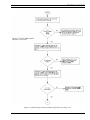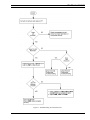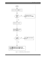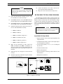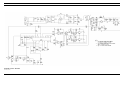
1
Maintenance Manual
DRC-200
DESKTOP REPEATER
450 - 470 MHz
ERICSSONZ
AE/LZB 119 1882 R1B
REVISION HISTORY
REVISION
DATE
REASON FOR CHANGE
R1A
9/96
Original
R1B
11/96
Corrected item 10 on page 11. Change phone numbers.
NOTICE!
This manual covers Ericsson and General Electric products manufactured and sold by Ericsson Inc.
NOTICE!
Repairs to this equipment should be made only by an authorized service technician or facility designated by the supplier. Any
repairs, alterations or substitution of recommended parts made by the user to this equipment not approved by the manufacturer
could void the user’s authority to operate the equipment in addition to the manufacturer’s warranty.
NOTICE!
The software contained in this device is copyrighted. Unpublished rights are reserved under the copyright laws of the
United States.
This manual is published by Ericsson Inc., without any warranty. Improvements and changes to this manual necessitated by
typographical errors, inaccuracies of current information, or improvements to programs and/or equipment, may be made by
Ericsson Inc., at any time and without notice. Such changes will be incorporated into new editions of this manual. No part of
this manual may be reproduced or transmitted in any form or by any means, electronic or mechanical, including photocopying
and recording, for any purpose, without the express written permission of Ericsson Inc.
Copyright© September 1996, Ericsson Inc.
2
AE/LZB 119 1882 R1B
TABLE OF CONTENTS
DESCRIPTION . . . . . . . . . . . . . . . . . . . . . . . . . .
INSTALLATION . . . . . . . . . . . . . . . . . . . . . . . . .
LOCATION CONSIDERATION . . . . . . . . . . . . . .
CABLE CONNECTIONS . . . . . . . . . . . . . . . . . .
HANDHELD MICROPHONE . . . . . . . . . . . . . . .
OPERATING CONTROLS AND INDICATORS . . . . . . . .
POWER ON/OFF Switch . . . . . . . . . . . . . . . . . .
VOLUME Control . . . . . . . . . . . . . . . . . . . . .
SQUELCH Control . . . . . . . . . . . . . . . . . . . . .
MONITOR Button . . . . . . . . . . . . . . . . . . . . . .
REPEAT Button . . . . . . . . . . . . . . . . . . . . . . .
REMOTE Button . . . . . . . . . . . . . . . . . . . . . .
REM Indicator . . . . . . . . . . . . . . . . . . . . . . . .
BZ Indicator . . . . . . . . . . . . . . . . . . . . . . . . .
TX Indicator . . . . . . . . . . . . . . . . . . . . . . . . .
MULTIFUNCTION CONNECTOR . . . . . . . . . . . . . . .
MULTIPLE CG/DCG DECODE . . . . . . . . . . . . . . . . .
OPERATION . . . . . . . . . . . . . . . . . . . . . . . . . . .
INITIAL . . . . . . . . . . . . . . . . . . . . . . . . . . .
GENERAL . . . . . . . . . . . . . . . . . . . . . . . . . .
PTT OPERATION . . . . . . . . . . . . . . . . . . . . . .
MAINTENANCE . . . . . . . . . . . . . . . . . . . . . . . . .
SIMPLIFIED TROUBLESHOOTING . . . . . . . . . . . . . .
SUMMARY OF DEALER’S PROGRAMMING OPTIONS . .
Channel Guard Tones (CTCSS) . . . . . . . . . . . . . . .
Digital Channel Guard Codes . . . . . . . . . . . . . . . .
ACCESSORIES . . . . . . . . . . . . . . . . . . . . . . . . . .
THEORY OF OPERATION . . . . . . . . . . . . . . . . . . . .
GENERAL INFORMATION . . . . . . . . . . . . . . . .
MAIN BOARD . . . . . . . . . . . . . . . . . . . . . . . . . .
RECEIVER SECTION . . . . . . . . . . . . . . . . . . .
TRANSMITTER/AUDIO CONTROL SECTION . . . . .
MICROPROCESSOR/DISPLAY BOARD . . . . . . . . . . . .
CONTROL BOARD . . . . . . . . . . . . . . . . . . . . . . .
POWER AMPLIFIER (PA) BOARD – 25 WATT . . . . . . . .
TRANSMIT RECEIVE SWITCH . . . . . . . . . . . . .
DC POWER DISTRIBUTION . . . . . . . . . . . . . . .
RF POWER LEVELING AND THERMAL SHUTDOWN
POWER SUPPLY MODULE . . . . . . . . . . . . . . . . . .
REAR PANEL DB-15 CONNECTOR I/O SPECIFICATIONS .
PTT PRIORITIES AND TX AUDIO DETAILS . . . . . . . . .
MAINTENANCE . . . . . . . . . . . . . . . . . . . . . . . . .
TROUBLESHOOTING . . . . . . . . . . . . . . . . . . . . . .
DUPLEXER REMOVAL AND REPLACEMENT . . . . . . . .
DUPLEXER TUNING PROCEDURES . . . . . . . . . . . . .
EQUIPMENT REQUIRED . . . . . . . . . . . . . . . . .
TUNING INSTRUCTIONS . . . . . . . . . . . . . . . . .
REPLACEMENT PARTS LISTS . . . . . . . . . . . . . . . . .
.
.
.
.
.
.
.
.
.
.
.
.
.
.
.
.
.
.
.
.
.
.
.
.
.
.
.
.
.
.
.
.
.
.
.
.
.
.
.
.
.
.
.
.
.
.
.
.
.
.
.
.
.
.
.
.
.
.
.
.
.
.
.
.
.
.
.
.
.
.
.
.
.
.
.
.
.
.
.
.
.
.
.
.
.
.
.
.
.
.
.
.
.
.
.
.
.
.
.
.
.
.
.
.
.
.
.
.
.
.
.
.
.
.
.
.
.
.
.
.
.
.
.
.
.
.
.
.
.
.
.
.
.
.
.
.
.
.
.
.
.
.
.
.
.
.
.
.
.
.
.
.
.
.
.
.
.
.
.
.
.
.
.
.
.
.
.
.
.
.
.
.
.
.
.
.
.
.
.
.
.
.
.
.
.
.
.
.
.
.
.
.
.
.
.
.
.
.
.
.
.
.
.
.
.
.
.
.
.
.
.
.
.
.
.
.
.
.
.
.
.
.
.
.
.
.
.
.
.
.
.
.
.
.
.
.
.
.
.
.
.
.
.
.
.
.
.
.
.
.
.
.
.
.
.
.
.
.
.
.
.
.
.
.
.
.
.
.
.
.
.
.
.
.
.
.
.
.
.
.
.
.
.
.
.
.
.
.
.
.
.
.
.
.
.
.
.
.
.
.
.
.
.
.
.
.
.
.
.
.
.
.
.
.
.
.
.
.
.
.
.
.
.
.
.
.
.
.
.
.
.
.
.
.
.
.
.
.
.
.
.
.
.
.
.
.
.
.
.
.
.
.
.
.
.
.
.
.
.
.
.
.
.
.
.
.
.
.
.
.
.
.
.
.
.
.
.
.
.
.
.
.
.
.
.
.
.
.
.
.
.
.
.
.
.
.
.
.
.
.
.
.
.
.
.
.
.
.
.
.
.
.
.
.
.
.
.
.
.
.
.
.
.
.
.
.
.
.
.
.
.
.
.
.
.
.
.
.
.
.
.
.
.
.
.
.
.
.
.
.
.
.
.
.
.
.
.
.
.
.
.
.
.
.
.
.
.
.
.
.
.
.
.
.
.
.
.
.
.
.
.
.
.
.
.
.
.
.
.
.
.
.
.
.
.
.
.
.
.
.
.
.
.
.
.
.
.
.
.
.
.
.
.
.
.
.
.
.
.
.
.
.
.
.
.
.
.
.
.
.
.
.
.
.
.
.
.
.
.
.
.
.
.
.
.
.
.
.
.
.
.
.
.
.
.
.
.
.
.
.
.
.
.
.
.
.
.
.
.
.
.
.
.
.
.
.
.
.
.
.
.
.
.
.
.
.
.
.
.
.
.
.
.
.
.
.
.
.
.
.
.
.
.
.
.
.
.
.
.
.
.
.
.
.
.
.
.
.
.
.
.
.
.
.
.
.
.
.
.
.
.
.
.
.
.
.
.
.
.
.
.
.
.
.
.
.
.
.
.
.
.
.
.
.
.
.
.
.
.
.
.
.
.
.
.
.
.
.
.
.
.
.
.
.
.
.
.
.
.
.
.
.
.
.
.
.
.
.
.
.
.
.
.
.
.
.
.
.
.
.
.
.
.
.
.
.
.
.
.
.
.
.
.
.
.
.
.
.
.
.
.
.
.
.
.
.
.
.
.
.
.
.
.
.
.
.
.
.
.
.
.
.
.
.
.
.
.
.
.
.
.
.
.
.
.
.
.
.
.
.
.
.
.
.
.
.
.
.
.
.
.
.
.
.
.
.
.
.
.
.
.
.
.
.
.
.
.
.
.
.
.
.
.
.
.
.
.
.
.
.
.
.
.
.
.
.
.
.
.
.
.
.
.
.
.
.
.
.
.
.
.
.
.
.
.
.
.
.
.
.
.
.
.
.
.
.
.
.
.
.
.
.
.
.
.
.
.
.
.
.
.
.
.
.
.
.
.
.
.
.
.
.
.
.
.
.
.
.
.
.
.
.
.
.
.
.
.
.
.
.
.
.
.
.
.
.
.
.
.
.
.
.
.
.
.
.
.
.
.
.
.
.
.
.
.
.
.
.
.
.
.
.
.
.
.
.
.
.
.
.
.
.
.
.
.
.
.
.
.
.
.
.
.
.
.
.
.
.
.
.
.
.
.
.
.
.
.
.
.
.
.
.
.
.
.
.
.
.
.
.
.
.
.
.
.
.
.
.
.
.
.
.
.
.
.
.
.
.
.
.
.
.
.
.
.
.
.
.
.
.
.
.
.
.
.
.
.
.
.
.
.
.
.
.
.
.
.
.
.
.
.
.
.
.
.
.
.
.
.
.
.
.
.
.
.
.
.
.
.
.
.
.
.
.
.
.
.
.
.
.
.
.
.
.
.
.
.
.
.
.
.
.
.
.
.
.
.
.
.
.
.
.
.
.
.
.
.
.
.
.
.
.
.
.
.
.
.
.
.
.
.
.
.
.
.
.
.
.
.
.
.
.
.
.
.
.
.
.
.
.
.
.
.
.
Page
6
7
7
7
7
7
8
8
8
8
8
8
8
8
8
8
9
9
9
9
9
10
10
10
11
12
12
13
13
13
13
13
14
14
14
15
15
15
15
15
18
20
24
32
33
33
34
35
3
AE/LZB 119 1882 R1B
FIGURES
Figure 1 - Front Panel Details . . . . . . . . . . . . . . . . . . . .
Figure 2 - Rear Panel Details . . . . . . . . . . . . . . . . . . . .
Figure 3 - DB15 Connector Pin Positions - Rear Panel View . . .
Figure 5 - Microphone Matching Network . . . . . . . . . . . . .
Figure 4 - Equipment Set-Up . . . . . . . . . . . . . . . . . . . .
Figure 6 - Test Probe A . . . . . . . . . . . . . . . . . . . . . . .
Figure 7 - Troubleshooting: Receiver Completely Dead . . . . . .
Figure 8 - Troubleshooting: Noise Present But No Signal Received
Figure 9 - Troubleshooting: No Transmit Power . . . . . . . . . .
Figure 10 - Troubleshooting: Receive Synthesizer . . . . . . . . .
Figure 11 - Troubleshooting: Transmit Synthesizer . . . . . . . .
Figure 12 - Duplexer Test Setup . . . . . . . . . . . . . . . . . .
Figure 13 - Duplexer Connections and Tuning Adjustements . . .
.
.
.
.
.
.
.
.
.
.
.
.
.
.
.
.
.
.
.
.
.
.
.
.
.
.
.
.
.
.
.
.
.
.
.
.
.
.
.
.
.
.
.
.
.
.
.
.
.
.
.
.
.
.
.
.
.
.
.
.
.
.
.
.
.
.
.
.
.
.
.
.
.
.
.
.
.
.
.
.
.
.
.
.
.
.
.
.
.
.
.
.
.
.
.
.
.
.
.
.
.
.
.
.
.
.
.
.
.
.
.
.
.
.
.
.
.
.
.
.
.
.
.
.
.
.
.
.
.
.
.
.
.
.
.
.
.
.
.
.
.
.
.
.
.
.
.
.
.
.
.
.
.
.
.
.
.
.
.
.
.
.
.
.
.
.
.
.
.
.
.
.
.
.
.
.
.
.
.
.
.
.
.
.
.
.
.
.
.
.
.
.
.
.
.
.
.
.
.
.
.
.
.
.
.
.
.
.
.
.
.
.
.
.
.
.
.
.
.
.
.
.
.
.
.
.
.
.
.
.
.
.
.
.
.
.
.
.
.
.
.
.
.
.
.
.
.
.
.
.
.
.
.
.
.
.
.
.
.
.
SPECIFICATIONS
(Subject to change without notice)
General
Regulatory Approval
FCC
DOC
Frequency Range/Model
Number of Channels
Operating Temperature
Frequency Stability
Antenna Impedance (RX and TX)
Speaker – Internal
– External
Supply Voltage
AC Line Protection
Connectors – Antenna
– Microphone
– Multifunction Port
– External Speaker
Size (H x W x D)
Weight
Receiver
Sensitivity – 12 dB SINAD
Threshold Squelch
Selectivity – 25 kHz
– 50 kHz
Intermodulation
Spurious Response
ARUDERU25B
491 195 162A
450-470 MHz
1
-30°C to +60°C
± 2.5 PPM, -30°C to +60°C
50 Ohms
8 Ohm, 2 Watts
3.2 Ohm, 5 Watts
120 VAC, 50/60 Hz; 105 Watts (@ 25W TX)
240 VAC, 50/60 Hz; 105 Watts (@ 25W TX)
4A Fuse, fast blow type
Type N, female (jack)
Modular, 6-pin
DB15, female
3.5mm jack
5.625" x 13.187" x 15.750"
13 lbs., 12 oz.
0.3 µV Max.
8 dB SINAD Max.
75 dB Min.
80 dB Min.
75 dB Min.
85 dB Min. (w/o duplexer)
Continued
4
.
.
.
.
.
.
.
.
.
.
.
.
.
.
.
.
.
.
.
.
.
.
.
.
.
.
Page
6
7
9
20
20
21
25
27
29
30
31
33
35
AE/LZB 119 1882 R1B
SPECIFICATIONS - Continued
(Subject to change without notice)
Receiver - Cont.
Audio Output
Audio Distortion
Attack Time
Closing Time
Unsquelched Hum and Noise
Squelched Hum and Noise
FCC
Transmitter
Operational Bandwidth
RF Output – Standard
– Low Power (programmable)
Spurious/Harmonics Emissions
FM Hum and Noise
Modulation
Audio Distortion
Attack Time
Time-Out Timer (programmable)
TX Hang Timer (programmable)
Identifier (programmable)
Tone Frequency
Modulation (40% ± 10%)
Transmission (Keying) Rate
Transmission Intervals
FCC Type Acceptance
2 Watts Max. (5 Watts External)
5% Max. @ 4.0 VRMS
50 ms Max.
100 ms Max.
45 dB Min.
-65 dBW Min.
Part 15
10 MHz
25 Watts Min. @ 50% Duty Cycle
10 Watts Min. @ Continuous
Adjustable from 2 Watts to 10 Watts
-70 dBc
-40 dB Min.
± 5 kHz
3% Max.
100 ms Max.
0, 15, 30 or 60 seconds; 2, 4, 8 or 16 minutes
0 to 15 seconds @ 1 second increments
Call sign in Morse code (CW); up to 8 characters
1215.9 Hz
± 2kHz (± 0.5 kHz)
21 – 22 WPM; Dot = 64 ms, Dash = 192 ms
15, 30, 60 or 90 Minutes; Once at first transmission after 10
minutes of inactivity
Part 90; Emission Designator 16K0F3E, 14K8F1D
Part 95; Emission Designator 16K0F3E
5
AE/LZB 119 1882 R1B
DESCRIPTION
NOTE
The DRC-200 is a state-of-the-art Desktop Repeater for
operation in the Land Mobile UHF (450-470 MHz) frequency band.
The repeater operates in the UHF band with a 25 watt
(without duplexer connected) RF output. Low power operation of 2 Watts is also available (Dealer programmable). The
built-in switching power supply automatically configures itself for operation on 120 VAC or 240 VAC, 50/60 Hz.
The unit features built-in Digital Channel Guard (DCG)
and standard Channel Guard (CG) tone squelch. In addition,
an external encoder and decoder can be utilized. A programmable CW Identifier is also included.
The radio has been programmed by the dealer. A list of
items determining the radio’s configuration should be available from the dealer. See page 10 for a list of Dealer Programming Options and page 41 for a blank form for
recording the Unit’s configuration. The radio’s program is
stored in non-volatile memory, which does not require a battery back-up.
In this manual, the words repeater, radio and unit are
used interchangeably.
See Figure 1 below for Repeater Front Panel details.
The Unit comes with the following standard accessories:
• Duplexer, installed
• Microphone Hang-up Clip with mounting hardware
• Operator’s/Installation Manual AE/LZT 123 1899
• Duplexer Tuning Manual AE/LZB 119 1910
Optional accessories include:
• Handheld Microphone with Coiled Cable
• Heavy Duty Desk Microphone
Figure 1 - Front Panel Details
6
AE/LZB 119 1882 R1B
INSTALLATION
3.
If used, plug in the External Speaker. This disconnects the Unit’s internal speaker.
4.
Install the microphone’s cable in the modular jack
located on the front panel. There will be a click
when the connector is fully seated.
5.
Plug the AC cord into a suitable 120 or 240 VAC
receptacle.
NOTE
It is recommended that the repeater and antenna installations be performed by a technician qualified in
2-way radio.
LOCATION CONSIDERATION
HANDHELD MICROPHONE
Choose a location for the radio that permits several
inches of clearance all around. This is necessary for proper
heat dissipation, especially around the heat sink mounted on
the rear panel.
CABLE CONNECTIONS
1.
Install the TX and RX antenna cables on their respective N type connectors. See Figure 2 below.
NOTE
When duplexer is used, antenna connection is
made to connector labeled ANTENNA.
2.
If used, plug in the cable to the Multifunction
Port’s DB15 connector. See page 8 for more details.
If a handheld microphone is used, a hang-up clip (supplied) can be mounted on the Unit’s right side near the front
panel. Using the one screw at the upper front corner and the
one approximately 2 1/2" below it, install the clip so that the
microphone’s hang-up button can be easily slid downward
in place.
OPERATING CONTROLS AND
INDICATORS
This section gives a brief description of each control,
button and status indicator. The OPERATION section provides more details on each of these and how they relate to
the unit’s overall operation.
As each button is pressed, a beep (if enabled; dealer programmable; see Page 10) will be heard. A high frequency
beep indicates the ON or enabled state, while a low frequency beep indicates the OFF or disabled state.
Figure 2 - Rear Panel Details.
7
AE/LZB 119 1882 R1B
POWER ON/OFF Switch
Power ON/OFF is a rocker switch. Press in at the top
end to turn the unit ON. Press in at the bottom end of it to
turn the radio OFF.
The indicator (LED) at the left end of the window (labeled POWER) should be lighted green when the unit is
ON.
REMOTE Button
Not used.
REM Indicator
Not used.
BZ Indicator
VOLUME Control
Use this knob to vary the receiver’s audio output level.
This also varies the audio level to an external speaker.
This green LED labeled BZ will be lighted whenever a
signal is received. In other words, the channel is busy (in
use).
SQUELCH Control
TX Indicator
NOTE
Do not turn the knob to maximum clockwise position. Turning the SQUELCH control significantly
past (clockwise) the threshold of quieting may adversely reduce receiver sensitivity and communications range.
Use this knob to eliminate speaker noise when not receiving a transmission. For proper operation, turn the knob
counter-clockwise until noise is heard. Then turn the knob
clockwise until the noise just disappears.
NOTE
When adjusting the squelch control, the Radio
should be in the MONITOR Mode.
When the repeater’s transmitter section is activated, the
red indicator labeled TX will be lighted.
MULTIFUNCTION CONNECTOR
The female DB15 connector, labeled MULTIFUNCTION PORT and located on the rear panel, provides for interfacing to a remote control device (DC, Tone or Local), an
Interconnect Control panel or for RS232 data input. See
Figure 3 for pin configuration. The purpose and/or specification of each pin is as follows:
Pin No.
1
Ground
2
Remote PTT; a low (ground) will cause the Unit to
transmit with User No. 1’s tone and the Remote TX
Audio (Pin 7).
3
Remote RX Audio Output; buffered de-emphasized
receiver audio.
4
Data PTT; a low (ground) will cause the Unit to
transmit with Data In audio (Pin 11).
5
Interconnect PTT; a low (ground) will cause the Unit
to transmit with User #16 tone and the Interconnect
TX Audio (Pin 14).
6
Switched +13.8 VDC; provides a low current (less
than 1 A) voltage source.
7
Remote TX Audio Input; is pre-emphasized by the
Unit.
8
Carrier Operated Signal (COS); output will be low
(transistor turned on) when the Repeater’s squelch
opens (breaks), regardless if Repeater’s audio is muted
or not.
MONITOR Button
Pressing this button toggles the unit into and out of the
Monitor Mode. When the unit is in the Monitor Mode, the
yellow LED labeled MON will be lighted. Also, any input
signal to the unit’s receiver can be heard, even if it has tone
coding such as CG or DCG.
REPEAT Button
Pressing this button toggles the unit into and out the Repeater Mode. The yellow LED labeled REP is lighted when
the Repeater Mode is enabled. The unit will NOT transmit
as a repeater unless the Repeater Mode is enabled.
Purpose/Specification
Continued
8
AE/LZB 119 1882 R1B
Continued
Pin No.
9
Purpose/Specification
Discriminator’s Audio Output; buffered unprocessed
(not de-emphasized) audio.
10
Interconnect RX Audio Output; buffered
de-emphasized receiver audio.
11
Data In; 4800 BAUD (2400 Hz) Maximum.
12
Remote Audio B. Not Applicable
13
External CG/DCG Input; modulates the
VCO/Reference Oscillator; External Encoding must
be selected for the Encode Tone.
14
Interconnect TX Audio Input; is pre-emphasized by
the Unit.
15
Interconnect Control Output; goes Low when User
#16 tone is decoded (or if the External Decode pin is
low).
erated as No. 18, it then cannot also be re-generated as No.
23 .
One of the 16 different tones or codes can be an input
from an external encoder. The external encoder signal has
priority over the Unit’s built-in encoder.
OPERATION
INITIAL
Turn on the unit. If squelch hasn’t been set yet, put the
unit into the Monitor Mode. If the yellow MON LED is not
lighted, press the MONITOR button. Set the Volume Control approximately to its 9 o’clock position. Then turn the
Squelch Control counter-clockwise until "noise" is heard.
At this time, the Volume Control can now be set for the
desired audio listening level. It can also be set later, when an
actual signal is being received. The Volume Control has no
effect on the transmitter audio.
Figure 3 - DB15 Connector Pin Positions
- Rear Panel View.
MULTIPLE CG/DCG DECODE
The unit’s built-in decoder can be programmed to accept
up to 16 different user’s CG tones or DCG codes and properly decode each one. There can be any combination of
tones or codes as long as the total is not more than 16. User
No. 16’s tone or code is always associated with Interconnect
Control.
The tone or code that is actually transmitted is not the
original one received, but one that is re-generated by the
unit. The generated tone or code can be a different tone or
code, as determined by the unit’s configuration programmed
by the dealer. For example, if the CG tone received is No.
12 (100.0 Hz), the Unit can be programmed to transmit No.
18 (123.0 Hz) or even a DCG code. However, a received
tone (or code) cannot be re-generated for more than one
tone (or code), whether it is the same or different tone
(code). For example, if received tone No. 12 is to be re-gen-
Now turn the Squelch knob clockwise slightly past the
point where the noise just disappears. This is the proper position for all normal squelched operations. If "noise" is occasionally heard, turn the Squelch Control slightly more
clockwise. If desired, the unit can now be taken out of the
Monitor Mode by pressing the MONITOR button. The
MON indicator should turn off.
GENERAL
If the unit is to be used as a self-controlling (receiver operation) repeater, press the REPEAT button to light the REP
LED.
PTT OPERATION
The operation of the radio’s PTT function has 5 priority
levels (1 being the highest) as follows:
1.
Local (front panel jack) microphone.
2.
Remote, if enabled (REM LED on).
3.
DATA (via DB15 connector).
4.
Interconnect Control panel.
5.
Receiver, if REPEAT Mode enabled (REP LED
on).
9
AE/LZB 119 1882 R1B
Although no repeater set-up would likely be configured
to accept all 5 PTTs, it is quite possible that at least two of
the five would be utilized. For example, the receiver’s PTT
action and the front panel’s PTT would probably be used
during the repeater’s initial installation and its checkout.
What the effect of prioritizing the various PTTs means is
that the TX audio of the PTT with the higher priority will
always be transmitted. For example, if the unit is receiving a
mobile unit, the audio being transmitted (repeated) is from
the receiver. Then if a remote control PTT is activated, the
audio from the remote is now transmitted (repeated).
NOTE
For In-Warranty service information, refer to the
Limited Warranty And Repair Information paragraph.
For future reference, please record:
Product Code ________________________________
FCC Identifier________________________________
MAINTENANCE
Serial No.____________________________________
NOTE
All adjustments affecting transmitter power output,
carrier frequency or modulation MUST be performed by a qualified electronics technician.
Date Purchased________________________________
Dealer_______________________________________
SUMMARY OF DEALER’S
PROGRAMMING OPTIONS
CAUTION
Do NOT tamper with internal adjustments. Damage to
the equipment and/or improper operation may result.
1.
Service Reminder
Have the Repeater checked periodically by a qualified
electronics technician using this Maintenance Manual,
AE/LZB 119 1882.
It should be noted that if no user tones (or codes)
are selected, the unit will respond to any carrier received. In other words, if the unit is in the Repeater
Mode it will repeat any carrier received, regardless
if the carrier is tone (or code) encoded or not.
SIMPLIFIED TROUBLESHOOTING
Perform the simple checks indicated below prior to returning the Unit for service.
Trouble
Check antenna connections.
No sound.
AC power cord.
Volume control setting.
Check External speaker connection.
Doesn’t repeat mobile’s
transmission.
Is REP indicator lighted?.
If not, press REPEAT button.
10
2.
Channel Guard Tones – any one of 50 CG Tones
can be programmed for any user. The Tone used for
a User’s decode (receive) tone can either be the
same, or different, from the user’s encode (transmit) tone. The same decode tone can not be used
for more than one user. However, the same encode
tone could be used for all 16 users if desired.
3.
Digital Channel Guard Codes – any one of 104
DCG Codes can be programmed for any user. The
Code used for a user’s decode (receive) code can
either be the same, or different, from the user’s encode (transmit) code. The same decode code can
Check
No reception.
Users – 1 to 16 users can be uniquely defined by:
their decode/encode tone or code; whether or not
there will be a courtesy beep; whether or not there
will be an encoding tone or code transmitted during Hang Time. User No. 1 is frequently referred to
as the "Boss tone". User No. 16 is reserved for Interconnect Control applications. A user may consist of one or many subscribers (or mobile units)
assigned to the same tone or code.
AE/LZB 119 1882 R1B
not be used for more than one user. However, the
same encode code could be used for all 16 users if
desired.
4.
5.
6.
7.
External Encoder/Decoder – any one of the 16 user
tones or codes can be programmed for using an external encoder.
Courtesy Beep – each user can be programmed to
provide a beep for 100 milliseconds after the originating transmission is stopped. This signals the receiving unit(s) that the originating unit has quit
transmitting.
Button Beep – the unit can be programmed to
either beep or not beep whenever one of the buttons (REPEAT, MONITOR) is pressed. A high frequency beep indicates the button’s associated
function is enabled. A low frequency beep indicates the function is disabled. Error beeps are not
affected by this Option’s selection.
Low RF Power – the unit can be set to High (Normal) RF Power Out or Low RF Power Out. Low
Power Out can be manually adjusted to approximately 2 Watts.
Channel Guard Tones (CTCSS)
8.
Time-Out Timer – the unit’s Time-Out (carrier control) Timer can either be disabled or set to allow a
transmission of 15, 30 or 60 seconds or 2, 4, 8 or
16 minutes duration.
9.
Hang Time – the unit’s Hang Time (drop-out delay) can be disabled (0 seconds) or set from 1 to 15
seconds, in 1 second increments. Hang Time is the
duration of time starting either with the release of
any PTT Switch or when the unit’s received carrier
drops while in the Repeater Mode.
10. Squelch Tail Eliminator – the unit can be set to
transmit a CTCSS tone at the end of a preset Hang
Time that is 180-degrees out of phase from the
tone transmitted during Hang Time.
11. CW Ident – the unit can be programmed to transmit a Continuous Wave (CW) Morse Code Identification (Ident) consisting of 1 to 8 characters
comprised of any of the 26 letters (standard English alphabet) and any number 0 through 9.
12. CW Ident Interval – the unit can be programmed to
send its CW Ident upon activation of any PTT (except DATA PTT) after every 15, 30, 60 or 90 minutes of activity. The unit will also automatically
send its CW Ident upon the first PTT (except
DATA PTT) after power up and after every 10 minutes of inactivity.
50 Tones
CTCSS tones are specified by a code number in the PC programmer. The following is the relationship between the code
number and the resulting CTCSS tone frequency in Hz.
Code
000 = No Tone = Carrier Squelch
001 = 67.0
011 = 97.4
021 = 136.5
031 = 192.8
041 = 165.5
002 = 71.9
012 = 100.0
022 = 141.3
032 = 203.5
042 = 171.3
003 = 74.4
013 = 103.5
023 = 146.2
033 = 210.7
043 = 177.3
004 = 77.0
014 = 107.2
024 = 151.4
034 = 218.1
044 = 183.5
005 = 79.7
015 = 110.9
025 = 156.7
035 = 225.7
045 = 189.9
006 = 82.5
016 = 114.8
026 = 162.2
036 = 233.6
046 = 196.6
007 = 85.4
017 = 118.8
027 = 167.9
037 = 241.8
047 = 199.5
008 = 88.5
018 = 123.0
028 = 173.8
038 = 250.3
048 = 206.5
009 = 91.5
019 = 127.3
029 = 179.9
039 = 69.4
049 = 229.1
010 = 94.8
020 = 131.8
030 = 186.2
040 = 159.8
050 = 254.1
11
AE/LZB 119 1882 R1B
Digital Channel Guard Codes
104 codes
CDCSS codes are specified by a code number in the PC programmer. The following is the relationship between the PC
programming code number and the resulting TIA/EIA CDCSS code and its inverted equivalent.
Code
DCS
Inv.
DCS
Code
DCS
Inv.
DCS
Code
DCS
Inv.
DCS
Code
DCS
Inv.
DCS
Code
DCS
Inv.
DCS
051
023
047
072
131
364
093
251
165
114
371
734
135
532
343
052
025
244
073
132
546
094
252
462
115
411
226
136
546
132
053
026
464
074
134
223
095
255
446
116
412
143
137
565
703
054
031
627
075
143
412
096
261
732
117
413
054
138
606
631
055
032
051
076
145
274
097
263
205
118
423
315
139
612
346
056
036
172
077
152
115
098
265
156
119
431
723
140
624
632
057
043
445
078
155
731
099
266
454
120
432
516
141
627
031
058
047
023
079
156
265
100
271
065
121
445
043
142
631
606
059
051
032
080
162
503
101
274
145
122
446
255
143
632
624
060
053
452
081
165
251
102
306
071
123
452
053
144
654
743
061
054
413
082
172
036
103
311
664
124
454
266
145
662
466
062
065
271
083
174
074
104
315
423
125
455
332
146
664
311
063
071
306
084
205
263
105
325
526
126
462
252
147
703
565
064
072
245
085
212
356
106
331
465
127
464
026
148
712
114
065
073
506
086
223
134
107
332
455
128
465
331
149
723
431
066
074
174
087
225
122
108
343
532
129
466
662
150
731
155
067
114
712
088
226
411
109
346
612
130
503
162
151
732
261
068
115
152
089
243
351
110
351
243
131
506
073
152
734
371
069
116
754
090
244
025
111
356
212
132
516
432
153
743
654
070
122
225
091
245
072
112
364
131
133
523
246
154
754
116
071
125
365
092
246
523
113
365
125
134
526
325
ACCESSORIES
The following accessories are available:
12
KRD 103 121/11
PC Programming Kit (consists of the following)
KRD 103 121/12
Programming Software
KRD 103 121/13
Instruction Sheet
KRD 103 121/14
Interface Adapter
KRD 103 121/15
Programming Cable
KRD 103 121/31
Handheld Microphone
AE/LZB 119 1882 R1B
THEORY OF OPERATION
GENERAL INFORMATION
The Repeater circuitry is distributed on five PC boards
as follows:
a.
Main PC Board containing the receiver section and
transmitter/audio control section
b.
Microprocessor/Display PC Board.
c.
Control PC Board which contains the audio and
squelch controls,
d.
PA PC Board.
e.
Power Supply module.
MAIN BOARD
RECEIVER SECTION
The receiver section uses 13.8 V DC from the Power
Supply module for the audio power amplifier U404. All
other circuits use regulated +10.0 volts from U405 or
U408, regulated +5.0 volts from U406 or U407, or regulated
-5.0 volts from the transmitter section.
The RF signal enters the receiver section via a 3 pole
helical resonator filter L401 and is amplified by a low noise,
wide dynamic range RF amplifier formed around Q401.
The signal then passes through a 4 pole helical resonator filter L404 before being feed to a double balanced mixer
HY401.
The receiver fractional-n synthesizer IC U403 receives
its frequency information from the microprocessor U201 on
the Microprocessor/Display board. The synthesizer uses a
12.8 MHz TCXO (2.5 PPM temperature compensated crystal oscillator) Y402 as the reference for the synthesizer frequency. The error voltage from the synthesizer IC is filtered
by a passive loop filter before being applied to the VCO
(voltage controlled oscillator) formed around Q404. The
VCO operates at the local oscillator injection frequency
21.4 MHz below the receive frequency. The VCO is buffered by Q405 and amplified by Q406. Q407 acts as a constant current source for Q406 to regulate the local oscillator
injection level to the mixer. The output of Q406 is coupled
to the double balanced mixer HY401.
The desired output of mixer HY401 is at 21.4 MHz and
is buffered by Q402 before being coupled to a 21.4 MHz six
pole crystal filter XF401. The filtered output is amplified
by Q403 before being applied to U401. Inside U401, the
21.4 MHz signal becomes the input to a second mixer with
an LO frequency of 20.945 MHz as determined by Y401.
The second mixer output at 455 kHz is filtered by a six pole
ceramic filter, CF401, then internally amplified and applied
to an FM detector. The detector output level is maximized
through adjustment of the quadrature detector coil L409.
The detected audio is buffered by U402D before being
routed to the Microprocessor/Display PC Board.
The detected audio from U402D is also routed to the
Squelch control R102 on the Control PC Board. The center
arm of the squelch control is routed to a high pass filter and
an amplifier internal to U401. U401’s output is routed to
an additional high pass filter U409B before being rectified
by CR401. The amount of ultrasonic noise on the detected
audio from U401 is used to determine the presence of an RF
carrier. The DC voltage from CR401 is routed to the Microprocessor/Display PC Board as an input to the microprocessor U201.
U404 is the audio power amplifier which drives either
the internal speaker or an external speaker.
TRANSMITTER/AUDIO CONTROL
SECTION
This section contains the -10.0 volt regulator U514
whose output is further regulated to -5 volts by U515. The
negative (–) 5 volt output is used by both the transmitter and
the receiver VCO’s. There are two +5.0 volts regulators
U510 and U511, as well as a +10.0 volt regulator U513, and
a switched +10.0 volt regulator U512 used for the transmit
VCO and transmit driver sections.
The unit has provisions for connecting local microphone
audio, remote station audio, interconnect audio, data or repeat audio to the transmitter’s modulation circuitry. These
audio signals, plus DCS, CTCSS or external tones, are controlled by information from the microprocessor U201 on the
Microprocessor/Display PC Board.
The microphone, remote, interconnect, data, and repeat
audio signals are routed through a preamp section before being connected to the multiplexer U502. The preamp sections are U503B for local microphone audio, U501A with
gain adjustment R553 for remote station audio, U501D with
gain adjustment R548 for interconnect audio, U503A for
buffering data and U501B with gain adjustment R507 for
repeat audio. The output of the multiplexer is routed to
U507B, U507C and U507D which form a limiter and two
stage (four pole) low pass filter. A master deviation control
R544 sets the signal level for the VCO modulation input
while the balance adjustment R538 sets the level for the
13
AE/LZB 119 1882 R1B
modulation of the transmit TCXO. For good broadband
transmit frequency response, both the TCXO and the VCO
are modulated. Two analog switches, U504A and U504C,
control whether external CTCSS tones are to be transmitted
or whether internal DCS or CTCSS signals are to be transmitted. These analog switches are controlled by Q516. An
optional DTMF code can be generated by the microprocessor. This code is amplified by U501C with R511 for deviation adjustment and connected to the audio limiter filter at
U507C.
Receiver audio from the main board is routed to the
CTCSS decoder/audio processor IC U204. This IC performs the CTCSS decoding and the primary muting of the
receiver audio. Audio from U204 is routed to an active filter
U205B which provides de-emphasis for the receiver audio
signal. It is then routed back to the main board and to audio
power amplifier, U404.
The transmitter fractional-n synthesizer IC U509 receives its frequency information from the microprocessor
U201 on the Microprocessor/Display Board. Like the synthesizer for the receiver local oscillator, this synthesizer uses
a 12.8 MHz TCXO (2.5 PPM crystal oscillator) Y501 for its
reference. The error voltage is filtered by the passive loop
before being applied to the transmit VCO formed around
Q509. The VCO operates at the transmitter frequency. The
VCO output is buffered by Q512 and amplified by Q513,
Q514 and Q515 and provides a drive level of approximately
250 milliwatts for the PA PC Board.
In addition, the base station model has a two digit display DP201, and integrated circuits U208 and U209 which
process the input from the channel selector switch, SW101,
on the control PC board.
Collector voltage is not applied to buffer amplifier transmitter Q514 until and unless both the receiver and transmitter VCO’s are in lock. ALC (automatic level control) dc
voltage is feedback from the PA PC Board to differential
amplifier U505A and comparator U505B. R526 and R528
set the voltage on the comparator for high and low power
output from the PA. The output of the comparator U505B
controls the supply voltage for Q513 and base bias of Q514.
Q503 and Q504 switch the drive required for high or low
power.
MICROPROCESSOR/DISPLAY
BOARD
The Microprocessor/Display PC Board contains the microprocessor U201 which provides data to the receiver and
transmitter synthesizers, data to the DTMF tone generator
U202 and U203, data to be latched into shift register U207
which controls LED indicators on the front panel, and data
to the receiver audio CTCSS decoder processor U204. U201
and U207 provides control information to the IC’s that control the transmitter audio paths on the main board. The microprocessor U201 generates the internal DCS and CTCSS
tones. The CTCSS tone is routed to an active 4 pole low
pass filter U211 and then to the main PC board to modulate
the transmitter. A 4 MHz crystal Y201 is shared by U201
and U204. The DTMF tone generator U203 uses a 3.579
MHz crystal Y202. All programmed information is stored
in a memory IC, U206.
14
A 5.0 volt regulator U210 supplies voltage to all active
components on the Microprocessor/Display PC board.
CONTROL BOARD
This board connects to the volume control R101, the
squelch control R102 and on base station models, the channel selection/scan switch SW101.
POWER AMPLIFIER (PA) BOARD –
25 WATT
The power amplifier module U301 is a hybrid amplifier
which can provide up to 25 watts of output power from the
250 milliwatts of drive provided by the transmitter section
on the main board. PLC1 and PLC2 form an RF pickup
loop that samples relative output power. This sampled output is rectified by CR301 and then filtered and amplified by
U302A and U302B. A thermistor temperature sensor provides for automatic power reduction if the power amplifier
module’s temperature limit is exceeded. The output from
U302A is the ALC (automatic level control) DC voltage
which is routed to the transmitter section of the main board
for control of the output power. U303 is a voltage regulator
for U302A and U302B.
A switched 13.6 volt source from Q505 supplies voltage
to the transmit/receive RF switch. Pin diodes CR302 and
CR303 connect the output power amplifier U301 to the antenna while shorting out the coax cable to the receiver. In
the repeater, the receiver is connected to its own antenna
connector rather than the cable from the PA board. Between
the transmit receive switch and the antenna connector is the
RF output low pass filter. The low pass filter components
are L306, L307, L308 and associated capacitors, C310,
C316, C317, C319 and C320.
AE/LZB 119 1882 R1B
TRANSMIT RECEIVE SWITCH
When the transmit 13.6 Volt line (Pin 3 of J301) becomes active, current passes through L316, R308, L311,
CR301, L315, CR302 and CR303 to ground. L316, C340,
C339, L311 and C338 isolate and bypass the RF. CR301
conducts RF from Q303 to the low pass filter. CR302 and
CR303 short to ground preventing RF from entering the receiver input P303. L315 along with the distributed capacitance form a high impedance path to ground, thus
preventing loss of transmit power.
During receive CR301 opens, disconnecting Q303.
CR302 and CR303 open, removing the short from the receiver path. L315, along with the distributed capacitance,
then forms a low pass pi section that passes the signal from
the antenna to the receiver input.
DC POWER DISTRIBUTION
DC power enters the PA Assembly from the power cable
assembly which is plugged into P301. The four leads in this
cord are:
1.
Red, Pin 1 = (+) or 13.6 VSW
2.
Black, Pin 2 = (–) or Ground
3.
Orange, Pin 3 and 4; Jumper between Pin 3 and 4
to 13.6 VSW
The Black wire should go directly to the negative terminal of the power supply module. The Red wire goes directly
to the positive terminal of the power supply module.
The Red wire, or high current path, goes directly to
Q303, Q302 and Q301 through L317 and R306. C329 bypasses the RF. CR305 protects this line from polarity reversal by blowing the fuse.
13.6 VSW enters at P301. CR304 protects this line
against polarity reversal. This 13.6 VSW line is connected to
the Main Board through the power interconnect cable and
Pin 1 of J301. This line is bypassed by C326 and C328. The
other pin connect of J301 is Pin 4 (ALC OUT), the sensing
voltage for thermal shut down and power leveling circuits.
A switched 13.6 volt source from Q505 supplies voltage
to the transmit receive switch. This voltage operates the TR
switch through line limiting resistor R308. This line supplies 13.6V to U301, the 8V regulator, and is bypassed by
C325.
RF POWER LEVELING AND THERMAL
SHUTDOWN
L318 and R310 form an RF pickup loop that samples
relative output power. This sampled output is rectified by
CR307 and filtered by C331, R309, R307 and C342.
Q305’s bias is set by variable resistor R317. The detected
output interacts with this variable DC voltage. R317 is used
to set Q305’s collector (the RF drive control line) to 4.3V at
45 Watts RF output. Any decrease in output power will
lower the detected voltage of CR307 causing Q305’s collector voltage to increase. This increased voltage is applied to
the ALC circuitry (on the Main board) which will increase
the exciter output power bringing the PA output power back
up to 45 Watts output. Any increase in the 45 Watts output
will have an opposite effect.
Q304 and RT301 form a temperature sensing circuit
with RT301 thermally connected to Q303. When Q303’s
case exceeds +90°C, Q304 will start to conduct which in
turn will increase the gain of Q305. Q305’s collector voltage will then be lower, causing the exciter output to decrease. This results in lower drive to the power amplifier,
allowing it to cool. RF output power is decreased but still allows lower power operation. C343 is a RF bypass.
POWER SUPPLY MODULE
The power supply module converts 120 volts or 220
volts at 50 Hz or 60 Hz to 13.8 volts DC. The power supply
is a switch mode type which operates at high efficiency to
keep internal temperatures low.
REAR PANEL DB-15 CONNECTOR
I/O SPECIFICATIONS
The function, description and specifications of each pin
of the Multifunction Port’s connector is as follows:
Pin Number: 1
Name:
GND
Description: Chassis and circuit ground. This point
serves as the voltage reference for the signals on all of the other pins.
Pin Number: 2
Name:
REMOTE PTT
15
AE/LZB 119 1882 R1B
Type:
Digital Input
Description: Unless superseded by a higher priority
PTT input (see Table 1), when the REM
LED on the front panel is illuminated, an
active level at this input will cause the
transmitter to transmit a carrier modulated
by the audio signal on the REMOTE TX
AUD input (pin 7).
Level:
This input is active with input voltages
less than 0.8 volts and inactive with input
voltages greater than 3.5 volts or when
left unconnected. Voltages between 0.8
and 3.5 volts should be avoided, except
during switching. Voltages below 0 volts
and above 5 volts should always be
avoided. The driving source should be
able to sink up to 5 mA to produce an active level.
Pin Number: 5
Name:
INTERCONNECT PTT
Pin Number: 3
Type:
Digital Input
Name:
REMOTE RX AUD
Type:
Analog Output
Description: Unless superseded by a higher priority
PTT input, an active level at this input
will cause the transmitter to transmit a
carrier modulated by the audio signal on
the INTRCNT. TX AUD input (pin 14).
Description: Buffered and squelched de-emphasized
receive audio output. This output is unbalanced to ground unless the optional
balanced 600 ohm interface board is installed. When this board is installed, this
output is one half of a balanced output.
The other half would be on Pin 12.
Impedance:
600 ohm nominal, AC coupled.
Level:
When the receiver is receiving a noise
quieted signal that is modulated at ± 3
kHz by a 1 kHz tone, this output will vary
between 75 mv and 1.5 volts RMS open
circuit depending upon the setting of
R480 on the main PC board.
Frequency
Response:
From 300 Hz to 3 kHz within +1/-3 dB of
a 6 dB/octave de-emphasis curve.
Pin Number: 4
16
Description: Unless superseded by a higher priority
PTT input, an active level at this input
will cause the transmitter to transmit a
carrier modulated by the signal on the
DATA IN input (pin 11).
Name:
DATA PTT
Type:
Digital Input
Level:
This input is active with input voltages
less than 0.8 volts and inactive with input
voltages greater than 3.5 volts or when
left unconnected. Voltages between 0.8
and 3.5 volts should be avoided, except
during switching. Voltages below 0 volts
and above 5 volts should always be
avoided. The driving source should be
able to sink up to 5 mA to produce an active logic level.
Pin Number: 6
Name:
+13.8VSW OUT
Type:
Analog Output
Description: This is the output of the internal 13.8 volt
power supply. Since this supply also supplies current for the radio, loads connected to this pin should be limited to less
than 1 A current drain. This line is unfused, except for the primary fuse inside
the power supply, but has internal shutdown on excessive load currents.
AE/LZB 119 1882 R1B
Pin Number: 7
Name:
REMOTE TX AUD
Type:
Analog Input
Description: This pre-emphasized audio input modulates the transmit carrier when the REM
LED is illuminated, when the REMOTE
PTT is taken to its active state and when
no higher priority PTT has been enabled.
Impedance:
600 ohms nominal, unbalanced.
Level:
Depending upon the setting of R553 (REMOTE AUDIO ADJ.) on the main board,
between 25 mv and 250 mv RMS nominal at 1 kHz will produce ± 3 kHz deviation.
Frequency
Response:
From 300 Hz to 3 kHz within +1/-3 dB of
a 6 dB/octave pre-emphasis curve.
Level:
An on-channel signal will produce 1.3
volts DC nominal into an open circuit.
Open circuit output level is 200 mv/kHz
nominal.
Frequency
Response:
Flat within +1/-3 dB, DC to 3 kHz.
Polarity:
Negative; an increase in frequency will
cause a reduction in ouput voltage.
Pin:
10
Name:
INTRCNT. RX AUD
Type:
Analog Output
Description: Buffered and squelched de-emphasized
audio output.
Impedance:
600 ohms nominal, AC coupled.
Level:
This output will be 350 mv RMS open
circuit nominal when the receiver is receiving a noise quieted signal modulated
at ± 3 kHz by a 1 kHz tone.
Frequency
Response:
From 300 Hz to 3 kHz within +1/-3 dB of
a 6 dB/octave de-emphasis curve.
Pin:
11
Name:
DATA IN
Type:
Analog/Digital Input
Pin Number: 8
Name:
COR OUT
Type:
Digital Output
Description: This is a transistor’s open collector to
ground output, which is active when a
carrier of sufficient level to operate the
BZ LED is being received.
Level:
When active, this output will remain at a
voltage less than 0.8 volts while sinking
up to 50 mA. When inactive, the leakage
current is less than 500 nA at voltages up
to 50 volts. Voltages above 50 volts may
damage the output transistor and should
be avoided.
Pin:
9
Name:
DISCR OUT
Type:
Analog Output
Description: Buffered, unsquelched output of the receiver discriminator.
Impedance:
600 ohms nominal, unbalanced, DC coupled.
Description: This flat (no pre-emphasis) input modulates the transmit carrier when the DATA
PTT is taken to its active state and no
higher priority PTT has been enabled.
This input is designed primarily for digital (logic level) signals, but can accept
analog signals of the proper level.
Impedance:
20 kohms, DC coupled.
Level:
For digital inputs, the two logic levels are
-15 to +0.5 volts and +3.5 to +15 volts.
With these levels, either standard
TTL/CMOS or RS-232 logic inputs may
be used. For analog inputs, a 100 mv
RMS signal nominal at 1 kHz will produce ± 3 kHz deviation. A capacitor in
17
AE/LZB 119 1882 R1B
series with analog inputs is required to
block the 1.8 volts DC present at this pin.
Frequency
Response:
Flat within +1/-3 dB, 5 Hz to 2.4 kHz.
Note: The input is DC coupled to allow
for proper switching of both TTL/CMOS
and RS-232 logic signals, but capacitive
coupling is used later in the audio chain
limiting the frequency response to 5 Hz
on the low end.
Digital bit streams are limited to 4800
baud maximum and should not have any
continuous string of 0’s or 1’s for longer
than 100 ms.
Name:
INTRCNT. TX AUD
Type:
Analog Input
Description: This pre-emphasized audio input modulates the transmit carrier when the INTERCONNECT PTT is taken to its active
state and when no higher priority PTT has
been enabled.
Impedance:
600 ohms nominal, unbalanced.
Level:
Depending upon the setting of R548 (INTERCONNECT AUDIO) on the main
board, between 25 mv and 250 mv RMS
nominal at 1 kHz will produce ± 3 kHz
deviation.
From 300 Hz to 3 kHz within +1/-3 dB of
a 6 dB/octave pre-emphasis curve.
Polarity:
Positive; the most positive input voltage
produces the highest carrier frequency.
Pin:
12
Name:
REMOTE AUDIO B
Frequency
Response:
Type:
Analog Output
Pin Number: 15
Description: Normally not connected.
Name:
INTRCNT. CONT
Pin Number: 13
Type:
Digital Output
Name:
EXT DCS/CTCSS
Type:
Analog Input
Description: This output goes to logic low state when
the receiver properly decodes User Tone
16 as programmed.
Description: External input for either DCS (CDCSS)
or CTCSS. The signal at this input is enabled through the programming software.
18
Pin Number: 14
Impedance:
10 kohm.
Level:
An input level between 250 mv and 750
mv RMS, depending upon the setting of
R581 (EXTERNAL CTCSS DEV. ADJ.),
on the main board is required to produce
700 Hz deviation of a 100 Hz tone.
Frequency
Response:
Within +1/-3 dB from 10 Hz to 300 Hz.
Polarity:
Negative; A positive input voltage change
will produce a negative frequency change.
Level:
Active low CMOS output. Logic low
level is 0 to 0.4 volts at up to a sink current of 6 mA. Logic high level is 3.7 to
5.0 volts when sourcing up to 6 mA.
PTT PRIORITIES AND TX AUDIO
DETAILS
The PTT function has 5 priority levels. The TX audio input associated with each priority level (source) is detailed in
Table 1 on the next page.
AE/LZB 119 1882 R1B
Table 1 - PTT Priorities and TX Audio Details vs. MUX Logic Levels
PTT
PRIORITY
SOURCE
PTT INPUT
1
Local
Microphone
2
Remote Audio
DB-15
Connector
Pin 2
3
Data Input
4
Interconnect
5
Receiver
AUDIO
INPUT
Mic. Connector Mic. Connector
Pin 3
Pin 4
INPUT LEVEL
LEVEL
FREQUENCY
RMS @ 1kHz ADJUSTMENT RESPONSE
MUX (U502)
Pin
9
Pin
10
Pin
11
6 mv
None
Pre-emphasized;
300 Hz to 3 kHz
0
1
0
DB-15
Connector
Pin 7
25 mv to 250
mv
R553
Pre-emphasized;
300 Hz to 3 kHz
0
1
1
DB-15
Connector
Pin 4
DB-15
Connector
Pin 11
TTL/CMOS
RS-232
100 mv Audio
None
Flat
5 Hz to 2.4 kHz
1
1
1
DB-15
Connector
Pin 5
DB-15
Connector
Pin 14
25 mv to 250
mv
R548
Pre-emphasized;
300 Hz to 3 kHz
0
0
1
Receiver
Squelch
De-emphasized;
Receive Audio
(only available
internally)
None
Pre-emphasized;
300 Hz to 3 kHz
0
0
0
NOTES: Priority 1 is the highest level.
"MUX" is an abbreviation for MULTIPLEXER.
0=0 to 0.8 volts
1=3.5 to 5.0 volts
19
AE/LZB 119 1882 R1B
panel VOLUME control to the mid-range position.
Connect an audio RMS voltmeter, SINAD meter,
and distortion meter, if available, to the speaker terminals.
MAINTENANCE
RECEIVER
For optimum performance, the unit should be realigned
before being put into service.
For base station units, set the unit to a receive frequency nearest the middle of the frequency list.
NOTE
Preliminary
1.
2.
Program unit for the desired frequency(ies) and
tones. Disable tone on a frequency at or near the
middle of the range of frequency(ies) programmed.
Set the front panel SQUELCH control to the maximum counter-clockwise position. Set the front
The maximum frequency spread is ± 5 MHz;
± 3 MHz for best sensitivity.
Figure 4 - Equipment Set-Up
Figure 5 - Microphone Matching Network
20
AE/LZB 119 1882 R1B
generator output level to keep the signal on the oscilloscope at 0.1 volt p-p.
VCO Tuning
3.
4.
Adjust C435 for a DC voltage of 2.75 ± 0.05 volts
at TP402. On base station units, check the maximum and minimum receive frequencies and insure
that the voltage at TP402 is between 1.6 and 4.4
volts.
Connect a frequency counter to the output of
TEST PROBE A. See Figure below. Hold TEST
PROBE A across R456 and adjust the trimmer capacitor inside Y402 so that the frequency counter
shows a frequency 21.4000 MHz below the receive
frequency to within ± 100 Hz.
Test Probe A is an RF coaxial cable with a 1000 pF, 50V
min. DC blocking capacitor placed in series with the center conductor. Observe proper polarity of the probe when
connecting the unit; one side is connected to test equipment ground.
Figure 6 - Test Probe A
IF Adjust
NOTE
The IF stages have been aligned at the factory
and should not normally require realignment
when the operating frequency range of the
unit is changed.
8.
Modulate the RF signal generator with a 1000 Hz
tone modulated at ±3.0 kHz. Set the signal generator output level to 100 microvolts (-67 dBm). Adjust L409 for maximum audio at the speaker
terminals. Readjust L408 and L407 slightly, if
necessary, for lowest distortion on the distortion
analyzer.
Front End Alignment
9.
Adjust L401A , B, and C and L404A, B, C, and D
(in that order) for maximum signal on the oscilloscope. Repeat once more. On base station units,
check at the maximum and minimum frequencies
and readjust, if necessary for good sensitivity at all
frequencies.
Remote Audio Output Adjustment
NOTE
This adjustment need only be made if the user
wishes to use the remote audio output.
10. Increase the signal generator output level to 1mv (47 dBm). Connect the audio voltmeter to pin 3 of
P502 on the rear of the unit.
11. Adjust R480 on the Main PC board for the desired
output level.
TRANSMITTER
Preliminary
NOTE
5.
Connect an oscilloscope to TP401.
6.
Connect an RF signal generator to the ANTENNA
Connector on the rear of the unit (on repeater units,
make sure the REP LED is off and do not connect
to the TX ANTENNA connector). Set the RF signal generator frequency to that of the unit and set
the RF output level such that a 0.1 volt p-p 455
kHz signal appears on the oscilloscope.
7.
Adjust L408 and L407 for maximum signal on the
oscilloscope. If necessary, reduce the RF signal
The transmitter PTT must be depressed to
make the following adjustments.
1.
For base station units, set the unit to a transmit frequency nearest the middle of the frequency list.
NOTE
Maximum frequency spread is ± 5 MHz; ± 3
MHz for best performance.
21
AE/LZB 119 1882 R1B
2.
Preset R528 (HI PWR Set) and R526 (LO PWR
Set) on the Main PC board fully counter-clockwise.
Deviation Adjustment
9.
Preset R544 (MASTER DEVIATION) and R583
(BALANCE) to mid-range.
VCO Tuning
3.
Adjust C545 for a DC voltage of 2.45 ± 0.05 volts
at TP501. On base station units, check the minimum and maximum transmitter frequencies to ensure that the DC voltage is between 1.0 and 4.0
volts.
4.
With a frequency counter connected to the output
of TEST PROBE A (see Figure 6), hold TEST
PROBE A across R593 and adjust the trimmer capacitor inside Y501 for a frequency on the frequency counter that is within ± 100 Hz of the
transmit frequency.
Exciter Tune-Up
5.
On base units, set the unit to a channel which is
programmed for high power. On repeater units, insure that the unit is programmed for high power.
6.
Set R526 (LO PWR Set) at mid range and set
R528 (HI PWR Set) fully clockwise. Connect a
wattmeter and RF power attenuator/dummy load
(50 watt minimum rating and 30 dB minimum attenuation) to the ANTENNA connector (TX ANTENNA connector on repeater units). Adjust
C566, C575, and C580 for maximum power output. Repeat once. The output power should exceed 25 watts.
10. For base station units, set the unit to a nontone/data channel. For repeater units, insure that
the unit has not been programmed for tones. Connect an FM demodulator through a power attenuator or a directional coupler to the output of the
transmitter. The de-emphasis function should be
turned off and all low pass and high pass filters in
the demodulator removed except for a low pass filter with a cutoff frequency greater than 15 kHz.
Connect the output of the demodulator to an oscilloscope.
11. Plug a dummy microphone circuit (see Figure 5)
into modular microphone jack on the front panel.
Connect an audio generator to the dummy microphone circuit and set the audio frequency to 1000
Hz . Adjust the output of the audio generator until
the sine wave on the oscilloscope just shows clipping on the peaks. Increase the audio level by 20
dB (factor of 10 in voltage).
12. Adjust R544 (MASTER DEVIATION) trimmer
for ± 4.2 kHz deviation. Change the frequency of
the audio generator to 300 Hz and adjust R583
(BALANCE) for ±4.2 kHz deviation. Observe the
demodulated signal on the oscilloscope. The correct waveform is shown below:
a.
Correct
b.
Incorrect
c.
Incorrect
Transmitter Auto Power Leveling Adjustment
7.
8.
22
For repeater units, if the unit is to be programmed
for high power, adjust R528 (HI PWR Set) for the
desired output power. If the unit is to be programmed for low power, skip to the following step.
On base station units, change to a channel which is
programmed for high power and adjust R528 for
the desired output power.
For repeater units, if the unit is to be programmed
for low power, re-program the unit for low power
and adjust R526 (LOW PWR Set) for the desired
output power. On base station units, change to a
channel programmed for low power and adjust
R526 for the desired output power.
AE/LZB 119 1882 R1B
13. Repeat steps 11 and 12 several times checking deviation and the demodulated waveform since R544
and R583 interact.
Internal DCS Adjustment
14. Preset R562 (INTERNAL DCS DEV. ADJ.) to
mid-range, if not already done.
15. Remove the 1000 Hz tone.
16. Set the unit to a channel programmed for a DCS
tone or on repeater units, program the unit for a
DCS tone.
17. Adjust R562 (INTERNAL DCS DEV. ADJ.) for ±
700 Hz deviation.
Internal CTCSS Adjustment
18. Set the unit to a channel programmed for a CTCSS
tone or on repeater units, program the unit for a
CTCSS tone.
DTMF/ID Tone Adjustment
24. Turn the unit OFF. Wait at least 30 seconds. Depress the T button (MON button on the repeater)
and activate the PTT while turning the unit on.
The unit should begin transmitting, with dual-tone
modulation for a base unit and single tone modulation for a repeater. The PTT switch and the T (or
MON) button may be released. The unit should
continue transmitting.
25. On base units, adjust R511 (DTMF ADJ.) for ± 3
kHz deviation. On repeater units, adjust R511 for
± 2 kHz deviation. Turn the unit OFF, wait at least
30 seconds and turn the unit back ON for the remainder of the alignment steps.
NOTE
A base unit’s test modulation is dual-tone,
while a repeater’s test modulation is single
tone.
Repeat Audio Adjustment
19. Adjust R556 (INTERNAL CTCSS DEV. ADJ.) for
± 700 Hz deviation.
External CTCSS/DCS Adjustment
NOTE
Repeater units only.
NOTE
This adjustment need only be performed if
the user wishes to transmit CTCSS and/or
DCS tones from an external source.
20. Connect a source of external tones to P502-13
(DB-15 Connector on rear panel).
21. Set the unit to a channel programmed to an external tone or for repeater units, program the unit for
external tones.
22. Adjust R581 (EXTERNAL TONE ADJ.) for ± 700
Hz deviation.
23. Reconnect the audio generator. Set the generator
for a 1000 Hz tone and check that ± 5 kHz deviation is not exceeded in any channel that was used
in step numbers 9 through 22. Repeat steps 9
through 22, if necessary.
26. Reprogram the unit so that no tones are programmed on receive. If the REP LED is not illuminated, depress the REPEAT button. The REP
LED should illuminate.
27. Connect an RF signal generator to the ANTENNA
(not TX ANTENNA) connector input on the rear
of the unit. Set the generator to the receive channel
frequency with an RF level of 100 microvolts and
with 1000 Hz tone modulated at ± 3.0 kHz deviation.
28. Adjust R507 (REPEAT AUDIO ADJ.) for ± 3.0
kHz deviation shown on the demodulator.
Interconnect Audio Adjustment
NOTE
This adjustment need only be made if the user
wishes to use the interconnect input.
23
AE/LZB 119 1882 R1B
29. Connect the audio generator to pin 14 of P502 on
the rear of the unit. The generator should be set for
a 1 kHz sine wave at the desired output level.
30. Ground pin 5 of P502. The unit should begin
transmitting.
31. Adjust R548 (INTERCONNECT AUDIO ADJ.) on
the Main PC board for ± 3.0 kHz deviation as
shown on the FM demodulator.
Remote Audio Adjustment
NOTE
This adjustment need only be made if the user
wishes to use the remote audio input.
34. Ground pin 2 of P502. The unit should begin
transmitting.
35. Adjust R553 (REMOTE AUDIO ADJ.) on the
Main PC board for ±3.0 kHz deviation.
The alignment process is complete. Reprogram the unit
for the desired tones and frequencies before putting the unit
in service.
TROUBLESHOOTING
Troubleshooting charts are given in Figures 7 thru 11.
The following lists the problems likely to be encountered,
and the reference figure and page numbers.
PROBLEM
32. Connect the audio generator to pin 7 of P502 on
the rear of the unit. The generator should be set for
a 1 kHz sine wave at the desired output level.
33. If the REM LED on the front panel is not illuminated, depress the REMOTE button. The REM
LED should now become illuminated.
24
Receiver Completely Dead
Noise Present But No Signal Received
No Transmit Power
Receive Synthesizer
Transmit Synthesizer
FIGURE NO.
7
8
9
10
11
AE/LZB 119 1882 R1B
Figure 7 - Troubleshooting: Receiver Completely Dead (Page 1 of 2)
25
AE/LZB 119 1882 R1B
Figure 7 - Troubleshooting: Receiver Completely Dead (Page 2 of 2)
26
AE/LZB 119 1882 R1B
Figure 8 - Troubleshooting: Noise Present But No Signal Received (Page 1 of 2)
27
AE/LZB 119 1882 R1B
Figure 8 - Troubleshooting: Noise Present But No Signal Received (Page 2 of 2)
28
AE/LZB 119 1882 R1B
Figure 9 - Troubleshooting: No Transmit Power
29
AE/LZB 119 1882 R1B
Figure 10 - Troubleshooting: Receive Synthesizer
30
AE/LZB 119 1882 R1B
Figure 11 - Troubleshooting: Transmit Synthesizer
31
AE/LZB 119 1882 R1B
DUPLEXER REMOVAL AND
REPLACEMENT
The following procedures should be followed to remove
and replace the duplexer.
1.
Turn off the Unit and unplug the AC Cord.
2.
Disconnect the TX and RX coaxial cables from the
rear panel.
3.
Remove the 8 black Phillips head screws that fasten the wrap to the chassis.
4.
Remove the wrap by sliding it off towards the rear
of the Unit.
5.
Remove the top cover, using a T9 TORX screwdriver for the 16 screws that hold the cover in
place.
6.
Remove the following cable connectors from the
Main Board Assembly:
10. Disconnect the following coax cables:
a.
P401’s miniature coax from rear panel’s lower
BNC connector labeled ANTENNA.
b.
PA Module’s RG-58 coax from rear panel’s
upper BNC connector labeled TX ANTENNA.
11. Place the Duplexer on the chassis bottom with its
BNC connectors towards the rear panel.
12. Fasten the Duplexer to the chassis bottom, using
the two supplied 8-32 black Phillips screws and
kepnuts. The screw heads go on the outside bottom.
13. Re-install the retaining bracket removed in Step 9.
Use the two holes in the center wall located towards the front of Unit The sponge rubber pad on
the bracket should be down on the Duplexer.
14. Install the supplied RG-58 coax cable.
a.
P401, 2-conductor, black, white wires.
b.
P501, 4-conductor, red brown orange. yellow
wires. This connector has a locking latch
which must be released before removal.
c.
P502, 1 pin 1 with orange wire.
d.
P503, 15-conductor; pin 1 with green wire.
e.
P504, 1 pin 1 with green wire.
f.
P505, 4-conductor; pin 1 with purple wire.
g.
P401, miniature coax; at front of Main Board.
h.
P501, miniature coax; at rear of Main Board.
a.
Connect one BNC end to the Duplexer’s center port labeled ANTENNA.
b.
Connect the other BNC end to the Unit’s
lower rear panel connector labeled ANTENNA.
NOTE
32
7.
Remove the 6 TORX (T9) screws that fasten the
Main Board Assembly in the chassis.
8.
Carefully lift the Main Board Assembly out of the
chassis.
9.
Remove the crossbrace (retaining bracket) by first
removing the 1 black Phillips screw from the chassis’ side. Lift up the end of the brace that was held
in by the screw and remove the brace from the
chassis.
Typically, the TX frequency is lower than
the RX Frequency. Thus, the normal connections to a Duplexer are: TX coax cable
to Low Pass Port; RX coax cable to High
Pass Port.
15. Connect the PA Module’s RG-58 coax cable to the
Duplexer’s port labeled LOW PASS.
16. Connect the P401’s miniature coax cable BNC end
to the Duplexer’s port labeled HIGH PASS. Dress
the miniature coax cable over the Duplexer with its
P401 end near the Unit’s front panel.
17. Carefully position the Main Board Assembly back
on the mounting flanges (feet) located on the center and right side walls. The proper orientation for
the Assembly is with the small heatsink and electrolytic capacitor- area located next to the side
wall.
AE/LZB 119 1882 R1B
25. Connect the antenna’s coax cable to the lower Ntype connector labelled ANTENNA.
NOTE
It may be easier to perform Steps 19 and 20 BEFORE the Main Board Assembly is fully lowered into place.
26. Plug in AC cord. The unit is now ready for use.
DUPLEXER TUNING PROCEDURES
18. Fasten the Main Board Assembly in place, using
the 6 TORX screws removed in Step 7.
19. Insert P401 (miniature coax) Into J401 located at
the front right corner of the Main Board Assembly.
20. Insert P501 (miniature coax) Into J501 located at
the rear right corner of the Main Board Assembly.
The following procedures must be used to tune the duplexer to the transmit and receive operating frequencies. The
duplexer must be retuned any time the frequencies change
or whenever the unit has been repaired or any module (duplexer, etc.) has been replaced. Refer to Figures 12 and 12
when performing these procedures for connections and tuning screws.
21. Install the following cable connectors into the center area of the Main Board Assembly:
NOTE
The duplex has been factory tuned for 462.675 MHz
transmit and 467.675 MHz receive frequencies.
a.
P401 (2-conductor)
b.
P501 (4-conductor)
c.
P502 (15-conductor, orange wire)
d.
P503 (15-conductor, blue wire)
e.
P504 (15-conductor, green wire)
• Signal Generator with 50 ohm output impedance and
output attenuator
f.
P505 (4-conductor, purple wire)
• Communications Monitor with 50 ohm input impedance and signal level indicator
EQUIPMENT REQUIRED
22. Make sure all connectors are fully seated. The
P401 (2-conductor) and P502 (15-conductor; orange wire) cables must be fully pushed down into
the notch In the center wall before the top cover is
installed.
• 50 ohm pads (quantity of 3); a 6, 10 or 20 dB pad
may be used
23. Install the top cover, using the 16 screws removed
in Step 5.
• Slotted screwdriver with long, narrow shaft to work
with nut driver
24. Slide the wrap back on and fasten in place with the
8 screws removed in Step 3.
• Phillips head screwdriver
• 50 ohm termination load
• Hollow shaft nut driver
Figure 12 - Duplexer Test Setup
33
AE/LZB 119 1882 R1B
TUNING INSTRUCTIONS
1.
2.
Turn off the DRC-200 with the front panel
POWER ON/OFF switch and unplug AC power
cord
Remove the eight (8) black Phillips head screws
that fasten the cover wrap to the chassis and slide
the cover wrap off towards the rest of the unit.
Disconnect the communications monitor and 50
ohm pad from the TX port and reconnect the cable
to the TX port that was removed in step 4.
10. Disconnect the cable from the RX port and connect
the communications monitor through the 50 ohm
pad to the RX port.
11. Tune the communications monitor to the transmit
frequency.
3.
Connect the signal generator output through the 50
ohm pad to the ANTENNA connector on the rear
panel.
4.
Disconnect the cable from the TX port on the duplexer and connect the communications monitor
through a 50 ohm pad to the TX port.
5.
Tune the communications monitor to the receive
frequency.
13. Adjust the three receiver port tuning screws for
minimum signal level on the communications
monitor. Adjustment of all three screws, one at a
time, may require that each screw be adjusted more
than once to obtain a minimum signal level indication.
6.
Unloosen the tuning screw shaft locking nuts (Figure 13) on all six. (6) tuning screws.
14. Tighten the tuning screw locking nuts after final
adjustment of the receiver port.
7.
Tune the signal generator to the receive frequency
and adjust for a high output.
8.
Adjust the three transmitter port tuning screws for
minimum signal level on the communications
monitor. Adjustment of all three screws, one at a
time, may require that each screw be adjusted more
than once to obtain a minimum signal level indications.
Tighten the tuning screw locking nuts after final
adjustment of the transmitter port.
34
9.
12. Tune the signal generator to the transmit frequency
and adjust for a high output.
15. Disconnect the cable from the RX port and reconnect the cable to the RX port that was removed in
Step 10.
16. Disconnect the signal generator and 50 ohm pad
from the ANTENNA connector on back panel.
17. Slide the cover wrap back on and fasten in place
with the eight (8) screws removed in Step 2.
AE/LZB 119 1882 R1B
Figure 13 - Duplexer Connections and Tuning Adjustements
REPLACEMENT PARTS LISTS
Replacement Parts are arranged in Tables 2 through 7 as
follows.
Figure references to the relevant parts placement diagrams are also included.
TABLE NO.
2
3
4
5
6
7
Parts labeling is per the following nomenclature:
Control Board
Microprocessor/Display Board
PA Board
Main Board
Power Supply Board
1XX
2XX
3XX
4XX, 5XX
XX
DESCRIPTION
NOTE
Replacement Parts List, Microprocessor/
Display Board
Replacement Parts List, PA Board
Replacement Parts List, Main Board
Replacement Parts List, Control Board
Replacement Parts List, Power Supply Board
Replacement Parts List, Miscellaneous Items
Any component described as "SMD" is a Surface
Mounted Device. All "Chip" capacitors and resistors
are also SMD type components.
35
AE/LZB 119 1882 R1B
Table 2 - Replacement Parts, Microprocessor/Display Board
ITEM REF. NUMBER
DESCRIPTION
ITEM REF. NUMBER
DESCRIPTION
R261, 273
R266
R267, 276
R268
R281
R283
R285, 286
R288, 289, 295, 296
Resistor, Chip; 15K Ohm, SMD
Resistor, Chip; 33K Ohm, SMD
Resistor, Chip; 470K Ohm, SMD
Resistor, Chip; 47K Ohm, SMD
Resistor, Chip; 15K Ohm, 2%, SMD
Resistor, Chip; 220K Ohm, 2%, SMD
Resistor, Chip; 0 Ohm, SMD
Resistor, Chip; 5100 Ohm, SMD
U201
U202, 207
U203
U204
U205, 211
U206
U210 (mounted on back)
IC; SMD
IC; SMD
IC, DTMF Generator; SMD
IC; SMD
IC, Op Amp; Dual; SMD
IC, EEPROM; SMD
IC, Regulator; 5.0V
Y201
Y202
Crystal, 4.0 MHz
Crystal, 3.579545 MHz
C201, 203
C202
C204, 228
C205, 207, 211, 214, 217, 232
C206, 209, 229, 245
C208, 220, 221, 235, 243, 244
C210, 216
C212, 213
C215
C218
C219
C225, 242, 246
C226, 227
C230, 231
C233
C234 (mounted on back)
C238
C239
C240
C241
Capacitor, Chip; .22 µF; SMD
Capacitor, Chip; 150 pF, 50V; SMD
Capacitor, Chip; 1000 pF, 10V; SMD
Capacitor, Tant; 1.0 µF, 35V; SMD
Capacitor, Chip; .01 µF; SMD
Capacitor, Chip; 470 pF, 50V; SMD
Capacitor, Chip; .1 µF, 50V; SMD
Capacitor, Chip; 33 pF, 50V; SMD
Capacitor, Tant; 22 µF, 16V; SMD
Capacitor, Poly; 0.15 µF
Capacitor, Chip; 1000 pF, 50V; SMD
Capacitor, Chip; .047 µF, 50V; SMD
Capacitor, Tant; 10 µF, 16V; SMD
Capacitor, Poly; .47 µF
Capacitor, Poly; .022mF
Capacitor, E; 470 µF, 16V
Capacitor, Chip; 2200 pF, 50V; SMD
Capacitor, Chip; .015 µF, 50V; SMD
Capacitor, Chip; 3300 pF, 50V; SMD
Capacitor, Chip; 6800 pF; SMD
CR201
CR202
CR203, 204, 205, 207, 215
CR210, 213, 214
CR211, 212
Zener; SMD
Diode, Zener
Diode, Dual; SMD
Diode; SMD
Diode, Silicon; SMD
J202
Connector, Header; 15-Pos.
L201
LD201, 206
LD202
LD203, 204, 205
Choke, 10 µH; SMD
Diode, LED; Green
Diode, LED; Red
Diode, LED; Yellow
P201 (mounted on back)
P203, 204 (mounted on back)
Connector, Header; 2-Pin
Connector, Header; 15-Pos.
Q201
Q202, 207, 215, 217, 219, 221
Q203, 204, 208, 212
Q210, 213, 214, 216, 218, 220
Q222
Transistor, NPN; SMD
Transistor, W/Bias; SMD
Transistor, NPN; SMD
Transistor, W/Bias; SMD
Transistor, W/Bias; SMD
C322, 323
C325, 326, 327, 328, 329
C326
C335
Capacitor, E; 10 µF, 25V
Capacitor, Chip; 3300 pF, 10V; SMD
Capacitor, Chip; 100 pF, 10V; SMD
Capacitor, Chip; 100 pF, 50V; SMD
Capacitor, E; 1 µF, 50V
Capacitor, HF; 3.9 pF .25pF, 200V; SMD
Capacitor, HF; 100 pF, 200V, 5%; SMD
Capacitor, Chip; 4 pF, 50V; SMD
Capacitor, HF; 4.3 pF .25 pF, 200V;
SMD
Capacitor, HF; 10 pF .5pF, 200V; SMD
Capacitor, HF; 8.2 pF .25 pF, 200V;
SMD
Capacitor, Chip; .01 µF, 10V; SMD
Capacitor, Feedthru; .001 µF
Capacitor, Chip; .22 µF; SMD
Capacitor, HF; 18pF, 200V, 5%; SMD
Resistor, Chip; 10K Ohm, SMD
CR301
CR302, 303
CR305
CR306
Diode, Schottky
Diode, Pin
Diode, Silicon, Rectifier
Diode, Silicon, Rectifier
JP301
Header, Right Angle
L301, 302, 303, 304, 309
L305
L306
L307, 308
Choke, LM-2; 10.5T
Coil, AW; 1.5T, 20 Awg
Coil, AW; 2.5T, 20 Awg
Coil, AW; 1.5T, 20 Awg
NOTE: All resistor values are 5%,
1/8W unless noted otherwise.
R201, 202, 203, 207, 214, 215,
216, 218, 220, 221, 222, 234,
236, 237, 239, 240, 241, 246,
253, 263, 270, 275, 290, 291,
292, 293
R204
R206, 212
R208, 277, 280
R209
R210, 278, 279
R211, 230, 269
R213, 229
R217
R219
R223
R224, 287
R225, 226
R228, 231
R232
R233
R235
R238, 245, 264, 265, 284
R242
R250, 251, 252
R254, 262
R258
R260, 272, 282, 294
36
Resistor, Chip; 4700 Ohm, SMD
Resistor, Chip; 12K Ohm, SMD
Resistor, Chip; 24K Ohm, SMD
Resistor, Chip; 16K Ohm, SMD
Resistor, Chip; 56K Ohm, SMD
Resistor, Chip; 22K Ohm, SMD
Resistor, Chip; 120K Ohm, SMD
Resistor, Chip; 100K Ohm, SMD
Resistor, Chip; 39 Ohm, SMD
Resistor, Chip; 1500 Ohm, SMD
Resistor, Chip; 2200 Ohm, SMD
Resistor, Chip; 270K Ohm, 1%, SMD
Resistor, Chip; 1.0M Ohm, SMD
Resistor, Chip; 150K Ohm, SMD
Resistor, Chip; 330K Ohm, SMD
Resistor, Chip; 2700 Ohm, SMD
Resistor, Chip; 470 Ohm, SMD
Resistor, Chip; 10 Ohm, SMD
Resistor, Chip; 180 Ohm, SMD
Resistor, Chip; 220 Ohm, SMD
Resistor, Carbon Film; 10 Ohm, 1/2W
Resistor, Chip; 68K Ohm, 2%, SMD
Socket, IC; SMD (for U201)
Table 3 - Replacement Parts, PA Board
ITEM REF. NUMBER
C301, 303, 305, 325
C302, 304, 306
C307, 321, 333, 334
C308, 313, 332
C309
C310
C311
C312
C316, 320
C317
C319
DESCRIPTION
NOTE: All resistor values are 5%,
1/8W unless noted otherwise.
R301
R302
R303
R304
R305
R306, 309
R307, 308
Resistor, Chip; 51 Ohm, SMD
Resistor, Met Oxide; 150 Ohm, 2W, 5%
Resistor, Chip; 33K Ohm, SMD
Resistor, Chip; 120K Ohm, SMD
Resistor Chip; 100K Ohm, SMD
Resistor, Chip; 10K Ohm, SMD
Resistor, Chip; 470 Ohm, SMD
RT301
Thermistor
TP1, 2
Contact Pin w/Star, .025 Sq.
U301
U302
U303
Module, RF PA
IC, Op Amp; Dual, SMD
IC, Regulator; 8.0V
AE/LZB 119 1882 R1B
Table 4 - Replacement Parts, Main Board
Table 4 - Replacement Parts, Main Board
ITEM REF. NUMBER
DESCRIPTION
ITEM REF. NUMBER
DESCRIPTION
L402
L403
L404
L407, 408
L409
L410, 412, 501, 503
L411
L413, 504
L414, 415, 505
L416
L506
Coil, AW; 16 Ga.
Coil, AW; 2.5T, Grn
Filter, Helical; 4-Sec.
Coil, IF; 21.4 MHz
Coil, IF
Choke, 390 nH; SMD
Choke, 0.27 µHy; SMD
Choke, 33 nH; SMD
Choke, 100 nH; SMD
Choke, 8.2 µH, 10%; SMD
Choke, 6T
Capacitor, E; 4.7 µF, 25V
Capacitor, E; 10 µF, 16V; SMD
P401
P501
P502, 503, 504
P505
Connector, Header, 2-Pin
Connector, Header, 4-Pin
Connector, Header, 15-Pos.
Connector, Header, 4-Pin
Capacitor, Chip; .047 µF, 50V; SMD
Capacitor, Chip; 68 pF, 50V; SMD
Capacitor, Chip; 47 pF; SMD
Capacitor, Chip; 330 pF; SMD
Capacitor, Chip; 1000 pF; SMD
Capacitor, Chip; 1800 pF; SMD
Capacitor, E; 1 µF, 50V
Capacitor, Chip; 470 pF; SMD
Capacitor, Poly Stkd; .22 µF
Capacitor, E; 2.2 µF, 50V; SMD
Q401, 405, 512
Q402
Q403
Q404, 509
Q406, 515
Q407
Q409, 507, 508, 516
Q503, 504
Q505, 506, 510
Q513
Q514
Transistor
Transistor, FET; SMD
Transistor, FET; SMD
Transistor
Transistor, RF Power
Transistor, PNP; SMD
Transistor, W/Bias; SMD
Transistor, W/Bias; SMD
Transistor, W/Bias; SMD
Transistor; SMD
Transistor; SMD
Capacitor, Poly Stkd; 0.1 mF
Capacitor, Trim; 2.5-10 pF; SMD
NOTE: All resistor values are 5%,
1/8W unless noted otherwise.
Capacitor, Chip; 15 pF, 50V; SMD
Capacitor, Chip; 12 pF, 50V; SMD
Capacitor, E; 100 µF, 16V
R401, 432
R402, 404, 405, 431
R403, 446, 471, 475, 620
R406, 449, 450, 451, 452, 454,
455, 465
R407
R408, 410
R409, 433, 436, 439, 445, 565,
575, 578, 586, 609
R411, 473, 537
R412, 442, 444, 570, 589
R413, 457
R414
R415, 531, 532, 539, 597, 607
R416, 611
R417
R418
R419, 424, 429, 579, 613
R420, 423, 447, 509, 514, 517,
518, 519, 520, 551, 554, 561,
573, 582
R421
R422, 425, 426, 427, 477, 478,
502, 505, 506, 508, 510, 521,
522, 523, 524, 525, 529, 559,
560, 605, 614, 619
R428, 515, 516, 547, 550, 610
R430, 461
R434, 437, 571, 576
R435
R438, 440, 464, 580, 590
R441, 588
R443, 530, 591, 594, 598, 599
R448, 533, 552, 555
R453, 456, 458, 595
R459, 600
R460, 566, 572
R462, 467, 568
R463
R468
R469
R470
C402, 407, 467, 490, 491, 549,
562
C403, 598, 599
C404, 409, 427, 451, 473, 480,
487, 511, 587, 590
C408, 426, 484
C410, 412, 413, 414, 425, 438,
439, 441, 446, 447, 448, 449,
452, 453, 454, 455, 456, 457,
461, 463, 465, 488, 493, 495,
517, 519, 533, 537, 538, 540,
542, 550, 552, 556, 558, 559,
560, 563, 564, 565, 570, 571,
572, 577, 579
C411
C415, 478, 479, 481, 483, 485,
486, 496, 581, 583, 585, 586,
588, 589, 592
C416, 417, 418
C419
C420
C421
C422, 423
C424
C428, 601
C429
C430, 489, 527
C431, 432, 433, 502, 504, 505,
510, 520, 531, 532, 593
C434, 458
C435, 545, 566, 575, 580
C436, 443, 444, 445, 547, 548,
554, 555, 557
C437, 450, 573
C440, 442, 462, 464, 472, 492,
509, 551, 553, 602
C459
C460
C466, 543, 603
C468, 476, 477, 497, 498, 513,
518, 595
C469
C470, 475
C471, 474, 596
C482, 594
C494
C499, 582
C501, 503, 512, 528
C506, 514, 516
C507
C515
C534
C535
C536
C539, 541, 569, 578, 591, 597
C544
C546
C561
C567, 576
C568
C574
C604
Capacitor, Chip; 100 pF, 50V; SMD
Capacitor, Chip; 470 pF, 50V; SMD
Capacitor, E; .47 µF, 50V
Capacitor, E; 470 µF, 16V
Capacitor, Chip; 2200 pF, 50V; SMD
Capacitor, Chip; 150 pF, 50V; SMD
Capacitor, Chip; 47 pF, 50V; SMD
Capacitor, Chip; 3300 pF; SMD
Capacitor, Chip; .015 µF; SMD
Capacitor, Chip; 0.1 µF, 25V; SMD
Capacitor, Chip; 4700 pF; SMD
Capacitor, Mylar; .022 mF, 100V
Capacitor, Poly Stkd; .33 µF
Capacitor, Mylar; .047 µF, 100V
Capacitor, Tant; 10 µF, 16V; SMD
Capacitor, Mylar; .0056 µF, 100V
Capacitor, Chip; 1.6 pF; SMD
Capacitor, Chip; 27 pF, 50V; SMD
Capacitor, Chip; 0.47 pF, 50V; SMD
Capacitor, Chip; 5 pF, 50V; SMD
Capacitor, Tant; 2.2 µF, 16V; SMD
Capacitor, Chip; 3.9 pF; SMD
CF401
Filter, Ceramic; 455 kHz
CR401
CR402, 403, 501, 502, 503
CR504
Diode, Dual; SMD
Diode; SMD
Diode, Silicon; SMD
HY401
Mixer Circuit
J401, 501
Min Pin Jack Typ Low
L401
Filter, Helical; 3-Sec.
Capacitor, Chip; 100 pF; SMD
Capacitor, Chip; .01 µF; SMD
Capacitor, Chip; 6.8 pF; SMD
Capacitor, Chip; 1000 pF; SMD
Capacitor, Poly; 1 µF, 63V
Capacitor, Poly Stkd; .47 µF
Capacitor, Chip; 10 pF, 50V; SMD
Capacitor, Chip; .1 µF, 50V; SMD
Resistor, Chip; 270 Ohm, SMD
Resistor, Chip; 56 Ohm, SMD
Resistor, Chip; 2200 Ohm, SMD
Resistor, Chip; 180 Ohm, SMD
Resistor, Chip; 150 Ohm, SMD
Resistor, Chip; 1800 Ohm, SMD
Resistor, Chip; 10 Ohm, SMD
Resistor, Chip; 3600 Ohm, SMD
Resistor, Chip; 68 Ohm, SMD
Resistor, Chip; 27 Ohm, SMD
Resistor, Chip; 68K Ohm, 2%, SMD
Resistor, Chip; 1000 Ohm, SMD
Resistor, Chip; 180K Ohm, SMD
Resistor, Chip; 6200 Ohm, SMD
Resistor, Chip; 3900 Ohm, SMD
Resistor, Chip; 470 Ohm, SMD
Resistor, Chip; 4700 Ohm, SMD
Resistor, Chip; 39K Ohm; SMD
Resistor, Chip; 10K Ohm, SMD
Resistor, Chip; 20K Ohm, SMD
Resistor, Chip; 1200 Ohm, SMD
Resistor, Chip; 330 Ohm, SMD
Resistor, Chip; 15 Ohm, SMD
Resistor, Chip; 51 Ohm, SMD
Resistor, Chip; 30K Ohm, SMD
Resistor, Chip; 100 Ohm, SMD
Resistor, Chip; 6800 Ohm, SMD
Resistor, Chip; 220 Ohm, SMD
Resistor, Chip; 5100 Ohm, SMD
Resistor, Chip; 3000 Ohm, 2%, SMD
Resistor, Chip; 33K Ohm, SMD
Resistor, Chip; 18K Ohm, SMD
Resistor, Carbon Film; 180 Ohm, 1/2W
Resistor, Chip; 2.7 Ohm, SMD
Resistor, Chip; 1 Ohm, SMD
37
AE/LZB 119 1882 R1B
Table 5 - Replacement Parts, Control Board
Table 4 - Replacement Parts, Main Board (Cont’d)
ITEM REF. NUMBER
DESCRIPTION
R472, 501, 503
R476, 558
R479
R480, 548, 553, 583
R504
R507, 544, 556, 562, 581
R511
R526
R527
R528
R534, 536
R535, 538, 541, 564
R540, 543
R542, 593
R545, 567, 596
R546
R549, 557, 563, 574, 603
R569
R577, 587
R592
R601
R602
R604
Resistor, Chip; 680 Ohm, SMD
Resistor, Chip; 150K Ohm, SMD
Resistor, Chip; 16K Ohm, SMD
Resistor, Variable; 100K, 20%, SMD
Resistor, Chip; 5600 Ohm, SMD
Resistor, Variable; 10K, SMD
Resistor, Variable; 200K, SMD
Resistor, Variable; 5K Ohm, 5MM
Resistor, Chip; 1500 Ohm, SMD
Resistor, Variable; 100K Ohm, 5MM
Resistor, Chip; 470K Ohm, SMD
Resistor, Chip; 22K Ohm, SMD
Resistor, Chip; 15K Ohm, 2%, SMD
Resistor, Chip; 12K Ohm, SMD
Resistor, Chip; 3300 Ohm, SMD
Resistor, Chip; 3.92K Ohm, 1%, SMD
Resistor, Chip; 100K Ohm, SMD
Resistor, Chip; 15K Ohm, SMD
Resistor, Chip; 39 Ohm, SMD
Resistor, Chip; 24K Ohm, SMD
Resistor, Chip; 750 Ohm, SMD
Resistor, Chip; 47 Ohm, SMD
Resistor, Chip; 75K Ohm, 1%, SMD
U401
U402, 501, 507
U403, 509
U404
U405, 408, 513
U406, 407, 510, 511
U409, 505, 508
U502
U503
U504
U506
U512
U514
U515
IC, IF Sys; SMD
IC, Op Amp; SMD
IC; SMD
IC, Audio
IC, Regulator; 10.0V
IC, Regulator; 5.0V; SMD
IC, Op Amp; Dual; SMD
IC; SMD
IC, Op Amp; SMD
IC, Analog Switch; SMD
IC; SMD
IC, Regulator; 10.0V; SMD
IC
IC, Regulator; Neg. 5.0V
XF401
Filter, Crystal; 21.4 MHz
Y401
Y402
Y501
Crystal, 20.945 MHz; Wire leads
Crystal, TCXO 12.8 MHz
Crystal, TCXO, 12.8 MHz
38
ITEM REF. NUMBER
DESCRIPTION
P101
P102
Jack, Right Angle Modular; Microphone
Connector, Header; 15 Pos.
R101
R102
Resistor, Var; 10K; Volume
Resistor, Var; 10K; Squelch
SW101
Switch, w/Push Sw (DBU)
AE/LZB 119 1882 R1B
Table 6 - Replacement Parts, Power Supply Board
ITEM REF. NUMBER
DESCRIPTION
ITEM REF. NUMBER
DESCRIPTION
T2
Transformer
BD1
Diode Bridge; 4A, 800V
U1
IC
C1, 4
C2, 3
C5, 6
C7
C8
C9, 10, 12, 16
C11
C13
C15
C17
C18, 19
C20
C24, 25, 30, 31
C29
C32
C34, 35
C36, 37
Capacitor, CD; 0.1µF, 250V
Capacitor, CD; 4700pF, 250V
Capacitor, E; 330µF, 200V
Capacitor, CD; 2.2µF, 250V
Capacitor, CD; 1500pF, 1000V
Capacitor, E; 1µF, 50V
Capacitor, CD; 2200pF, 50V
Capacitor, Mylar; 0.001µF, 50V
Capacitor, Mylar; 0.022µF, 50V
Capacitor, CD; 330pF, 50V
Capacitor, CD; 0.1µF, 100V
Capacitor, E; 47µF, 50V
Capacitor, CD; 0.01µF, 100V
Capacitor, E; 4.7µF, 50V
Capacitor, CD; .02µF, 1000V
Capacitor, E; 2200µF, 35V
Capacitor, CD; 0.01µF, 1000V
VR1
Potentiometer, 1K; Voltage Adjust
ZD1
ZD2, 3
Diode, Zener; 16.1V
Diode, Zener; 33V, 1W
ZNR1, 2, 3, 4, 5
Zener, Avalanche
CN1
CN2
CN3
Connector, Header; 2-Pin
Connector, Header; 3-Pin
Connector, Header; 2-Pin
D1, 2
D3, 4
D6, 9, 10, 12, 18
D13
D15, 16
Diode,
Diode, 1N4001
Diode, 1N4148
Diode,
Diode,
L1
Inductor, Toroid
LF2
Filter, Line
Q1, 2
Q3, 4
Q5
Q6, 7
Transistor, NPN
Transistor, NPN
Transistor, NPN
Transistor, PNP
Shield, Power Supply
Screw, 4-40 x 5/16 PPH; Qty. 4; PCB
Mtg.
Screw, 4 x 1/4, Type AB; Qty. 4; Shield
Mtg.
NOTE: All resistors are 5%,
1/4W unless specified otherwise.
R1, 2
R3
R6
R7, 10, 15, 17
R8, 11
R9, 12
R13, 14
R16, 18, 42, 44, 45
R19
R20, 23
R21, 34, 46
R22
R24
R25
R31
R32
R33
R35
R36, 47
R37
R40
R43
R41
R48
R49, 50
Resistor, Carbon Film; 150K, 1/2W
Resistor; 51Ohm, 5W
Resistor, Carbon Film; 680K Ohm,
1/2W
Resistor, Carbon Film; 2.7K Ohm
Resistor, Carbon Film; 10 Ohm
Resistor, 390K Ohm, 1%, 1/2W
Resistor, Carbon Film; 2.2 Ohm 1/2W
Resistor, Carbon Film; 1K Ohm
Resistor, Carbon Film; 22K Ohm
Resistor, Carbon Film; 5.6K Ohm
Resistor, Carbon Film; 47K Ohm
Resistor, Carbon Film; 33K Ohm
Resistor, Carbon Film; 100K Ohm
Resistor, Carbon Film; 1.8K Ohm
Resistor, Carbon Film; 470 Ohm
Resistor, Carbon Film; 9.1K Ohm
Resistor, Carbon Film; 390 Ohm
Resistor, Carbon Film; 1.5K Ohm, 1/2W
Resistor, Carbon Film; 10K Ohm
Resistor, 270 Ohm, 2W
Resistor, 5.6 Ohm
Resistor, Carbon Film; 3.3K Ohm
Resistor, Carbon Film; 47 Ohm
Resistor, Carbon Film; 7.5K Ohm
Resistor, Carbon Film; 10 Ohm, 1/2W
RTH1, 2
Thermistor
SW1
Switch, Slide; Select 110/220 VAC
T1
Transformer
39
AE/LZB 119 1882 R1B
Table 7 - Replacement Parts, Miscellaneous
ITEM REF. NUMBER
DESCRIPTION
F1
Fuse, 4 Amp; 3 AG, 250V
J1
J2
J3, J4
Jack, 3.5MM Phone; w/Nut
Cable Assembly, 15 Cond.;
Multifunction Port
Connector, BNC to N; Qty. 2
PS1
PCB Assembly, Power Supply
SPKR1
Speaker, 8 Ohm
SW1
Switch, Rocker; ON/OFF
Bracket, Ground; Qty. 2
Bracket, Duplexer Retainer (DRU)
Foot, Rubber; Qty. 4
Chassis
Front Panel, Desktop
Top Cover
Keyboard (Button); Qty. 3
Fuse Holder; w/Nut and Washer
Lug, Solder; Qty. 1
Connector, BNC, Female
Terminal Ring
Connector, Screw Lock; Qty. 2
Knob, Volume/Squelch; Qty. 2
Shield, VCO
Shield, VCO; Qty. 2
Shield, Power Supply
Shield, PA Mod.
Shield, Bottom; Qty. 2
Shield, Partition
Shield Walls; Qty. 2
Top Shield; Qty. 2
Shield, Spur Radiation
Display, Mask
Plate, PA End
Spacer, Module
Screw, 4-40 x 5/16; Cad/Zinc; Qty. 2
Screw, 4-40 x 5/16; Qty. 4
Screw, 6-32 x 1/2; Qty. 4
Screw, 6-32 x 3/8; Qty. 13 (DRU)
Screw, 8-32 x 3/8; Qty. 2
Screw, Pushtite, 4 x 5/16; Qty. 8
Screw, Pushtite, 4 x 1/4; Qty. 4
Screw, 4 x 1/4; Qty. 31
Standoff; Qty. 10
Screw, 4-40 x 1/4; TORX; Qty. 27 (DRU)
Screw, 4-40 x 1/4; Pan Head; Qty. 4
Screw, 4-40 x 3/8; TORX; Qty. 12
Hang Up Clip; Microphone
Grommet, Rubber
Grommet, Flex Strip
Washer, 1/8 x 9/32 x 032CD; Qty. 4
Washer, Solder; Qty. 5
Kep Nut, 4-40 x 1/4 St Cad; Qty. 2
Kep Nut, 8-32 x 11/32, Cad/Zinc; Qty. 2
Lens (DRU)
Heatsink; Qty. 2
Heatsink
Strain Relief
Cord, AC w/Plug
Instruction Manual (DBU)
Cable Assembly, Coax
Cable Assembly, Coax (DRU)
Cable Assembly, Coax; w/BNC
Wire Assembly, Black
Wire Assembly, Black
Cable Assembly, 2 Cond.
Cable Assembly, 15 Cond.
Cable Assembly, 15 Cond.
Cable Assembly, 4 Cond.
Cable Assembly, 4 Cond.
Cable Assembly, 2 Cond.
40
SERVICE PARTS
The following parts will be available as replacement parts.
RV/1411-7112-502
RV/5115-5343-801
RV/2402-5384-204
RV/1301-3299-602
RV/7011-2166-900
RV/7011-2204-300
RV/7011-2124-600
FRONT PANEL
SWITCH
VOLUME/SQUELCH KNOB
SPEAKER
MAIN BOARD
PA BOARD
MICROPROCESSOR BOARD
AE/LZB 119 1882 R1B
You may use this form to record the Unit’s configuration.
User
Memo
Decode
Tone (Hz)
or Code
Encode
Tone (Hz)
or Code
Encode
During
Hang Time
Courtesy
Beep
Y/N
Y/N
Notes/Comments
1
2
3
4
5
6
7
8
9
10
11
12
13
14
15
16
Receive Frequency:
MHz
Transmit Frequency:
MHz
RF Output Power:
(High/Low
or record Watts)
Beep on Button Press:
(Yes/No)
Time-Out Timer:
❑ Seconds❑ Minutes
Hang Time:
Seconds
CW Ident Interval:
Minutes
CW Ident:
(up to 8 characters)
NOTE: This page only may be copied without violating copyright.
41
AE/LZB 119 1882 R1B
CONTROL BOARD
(305-187, Rev. A)
(305-684, Rev. A)
42
BLOCK DIAGRAM
AE/LZB 119 1882 R1B
BLOCK DIAGRAM
(701-174, Rev. C)
43
AE/LZB 119 1882 R1B
MAIN (COMPOSITE) BOARD
(701-215, Sh. 1, Rev. A)
(701-216, Sh. 1, Rev. A)
44
SCHEMATIC DIAGRAM
SCHEMATIC DIAGRAM
AE/LZB 119 1882 R1B
MAIN (COMPOSITE) BOARD
(701-215, Sh. 2, Rev. A)
(701-216, Sh. 2, Rev. A)
45
AE/LZB 119 1882 R1B
MICROPROCESSO/DISPLAY BOARD
(701-130, Rev. M)
(701-203, Rev. M)
46
SCHEMATIC DIAGRAM
SCHEMATIC DIAGRAM
AE/LZB 119 1882 R1B
PA BOARD
(602-752, Rev. A)
(602-753, Rev. A)
47
AE/LZB 119 1882 R1B
POWER SUPPLY BOARD
(602-589, Rev. B)
48
SCHEMATIC DIAGRAM
SERVICE OUTLINE
AE/LZB 119 1882 R1B
MICROPROCESSOR/DISPLAY BOARD
(305-536, Rev. C)
49
AE/LZB 119 1882 R1B
PA BOARD
(305-537, Rev. C)
50
SERVICE OUTLINE
SERVICE OUTLINE
AE/LZB 119 1882 R1B
MAIN BOARD
(305-703, Rev. A)
51
Ericsson Inc.
Private Radio Systems
Mountain View Road
Lynchburg, Virginia
1-800-592-7711 (Outside USA, 804-592-7711)
AE/LZB 119 1882 R1B
Printed in U.S.A.