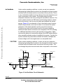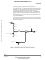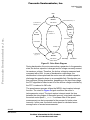
1
Freescale Semiconductor, Inc.
16
Order this document
by AN1857/D
Motorola Semiconductor Application Note
Freescale Semiconductor, Inc...
AN1857
A 3-Phase ac Induction Motor Control System
Based on the MC68HC908MR32
By: Bill Lucas and Ken Berringer
Motorola Microcontroller Division
Austin, Texas
Software Written By:
Radim Visinka, Petr Lidak, Pavel Kania, and Petr Stekl
Roznov System Application Laboratory
Roznov, Czech Republic
Introduction
The use of microcontroller technology has enabled the design of energyefficient and cost-effective motor control systems. Using
microcontrollers (MCU) with specialized pulse-width modulator
interfaces and integrated protection architecture allows a reasonable
approach to reduce total system cost and increase overall performance.
This application note describes such a system based on the Motorola
MC68HC908MR32 (MR32) motor control specific MCU, optoisolation,
and power electronics.
A discussion of the MR32 MCU, hardware design of the control board,
optoisolation interface, power electronics, and the required software to
control a 3-phase induction motor is presented.
© Motorola, Inc., 2000
AN1857
For More Information On This Product,
Go to: www.freescale.com
Freescale Semiconductor, Inc.
Application Note
A Look at the MC68HC908MR32 Motor Control Microcontroller
The MR32 is a new member of the low-cost, high-performance
M68HC08 (HC08) Family of 8-bit MCUs that are designed specifically for
midrange motor control applications.
Freescale Semiconductor, Inc...
The Motorola HC08 Family of MCUs is an enhanced, upward object
code compatible architecture that evolved from the M68HC05 (HC05)
Family. All MCUs in the family use the enhanced HC08 central
processor unit (CPU08) that includes new addressing modes, many new
instructions, and the performance improvements to existing instructions
that result from the introduction of instruction pipelining. MCUs in the
HC08 Family are available with a variety of package types, input/output
(I/O) modules, and various memory sizes and types.
Features of the MR32 motor control MCU include:
•
High-performance M68HC08 (CPU08) architecture
•
Fully upward-compatible object code with M68HC05, M146805,
and M68HC(7)05 Families
•
8-MHz internal bus frequency
•
32 Kbytes of on-chip FLASH memory
•
FLASH data security
•
768 bytes of on-chip random-access memory (RAM)
•
12-bit, 6-channel center-aligned or edge-aligned pulse-width
modulator (PWMMC) module
•
Serial peripheral interface module (SPI)
•
Serial communications interface module (SCI)
•
16-bit, 4-channel timer interface module (TIMA)
•
16-bit, 2-channel timer interface module (TIMB)
•
Clock generator module (CGM)
•
Digitally filtered low-voltage inhibit (LVI)
•
10-bit, 10-channel analog-to-digital converter (ADC)
AN1857
2
MOTOROLA
For More Information On This Product,
Go to: www.freescale.com
Freescale Semiconductor, Inc.
Application Note
A Look at the MC68HC908MR32 Motor Control Microcontroller
Freescale Semiconductor, Inc...
System protection features include:
•
Optional computer operating properly (COP) reset
•
Low-voltage detection with optional reset
•
Illegal opcode detection with optional reset
•
Illegal address detection with optional reset
•
Fault detection with optional PWM disabling
•
Low-power design, fully static with wait mode
•
Master reset pin (RST) and power-on reset (POR)
•
64-pin plastic quad flat pack (QFP)
Some CPU08 features include:
•
Enhanced M68HC05 programming model
•
Extensive loop control functions
•
16 addressing modes (eight more than the HC05)
•
16-bit index register and stack pointer
•
Memory-to-memory data transfers
•
Fast 8 by 8 bit multiply instruction
•
Fast 16/8 bit divide instruction
•
Binary-coded decimal (BCD) instructions
•
Optimization for controller applications
•
Improved C language support
This application note does not discuss in great detail each of the I/O
modules resident on the MR32. Figure 1 shows a block diagram of the
MR32. For a detailed description of the MR32, refer to 68HC908MR32,
68HC908MR16 Technical Data: Advance Information, Motorola
document order number MC68HC908MR32/D.
The MR32’s PWMMC module and its protection features make the
device an excellent choice for use in an embedded motor control
system. A review of the PWMMC module and its features is included
here.
AN1857
MOTOROLA
3
For More Information On This Product,
Go to: www.freescale.com
Freescale Semiconductor, Inc.
Application Note
TIMA
4-CH
10-CH
10-BIT
SPI
SCI
LVI
TIMB
2-CH
Freescale Semiconductor, Inc...
ADC
CPU08
32K FLASH
SIM
768 BYTES RAM
CGM
13 I/0 PIN
PWM1
PWM2
PWM3
PWM4
PWM5
PWM6
PWMMC
POLARITY
SIGNALS
FAULT
INPUTS
Figure 1. MC68HC908MR32 Block Diagram
MC68HC908MR32 Pulse-Width Modulator
The pulse-width modulator module (PWMMC) resident on the MR32 is
specifically designed to provide pulse-width modulated outputs to drive
a power stage connected to a dc servo, brushless dc, or 3-phase ac
motor system. The PWMMC module can be partitioned and configured
in several ways, depending on the specific motor control application.
Figure 2 shows a block diagram of the PWMMC module and is
referenced throughout this explanation of the PWMMC generator.
Features of the MR32 PWM include:
•
Three complementary PWM pairs or six independent PWM
signals
•
Complementary mode features include:
– Dead-time insertion
– Separate top/bottom pulse-width correction via current
sensing or programmable software bits
•
Edge-aligned PWM or center-aligned PWM signals
•
PWM signal polarity
•
20-mA current sink capability on all PWM outputs
•
Manual PWM output control through software
•
Programmable fault protection
AN1857
4
MOTOROLA
For More Information On This Product,
Go to: www.freescale.com
Freescale Semiconductor, Inc.
Application Note
MC68HC908MR32 Pulse-Width Modulator
OR
UP/DOWN
COUNTER
PRESCALER
÷ 1, 2, 4, OR 8
÷ 1, 2, 4,O R 8
PWM
GENERATORS
COMPARATORS
DOUBLE
BUFFERED
REGISTERS
Freescale Semiconductor, Inc...
PRESCALER
CONTROL
FAULT
PROTECTION
PWM
MODE
SELECT
OUTPUT
PWM1
PWM2
DEADTIME
INSERTION
FAULT
PARTITIONING
POLARITY
CONTROL
PWM3
PWM4
DIRECT
OUTPUT
CONTROL
DISTORTION
CORRECTION
MOTOR CURRENT POLARITIES
PWM RELOAD
AND INTERRUPT
INTERRUPTS
FAULT
MODE
SELECT
HIGH
CURRENT
DRIVERS
PWM5
PWM6
SYSTEM FAULTS
Figure 2. PWMMC Module Block Diagram
One of the most important features of the PWMMC is its ability to “shut
itself down” when a system fault is detected. When dealing with a system
that potentially could have hundreds of amps of peak current, reacting to
faults such as overcurrent or overvoltage conditions is an absolute
necessity. Fault protection is discussed here first. We then work our way
from the outputs of the PWM inward. A discussion of the inputs to the
PWM follows.
The six outputs of the PWMMC generator can be configured as
individual pulse-width modulated signals where each output can be
controlled as an independent output. Another option is to configure the
outputs in pairs, with the outputs complementary or not, so driving
complementary top and bottom transistors on a power stage becomes
an easy task. The outputs of the PWMMC are capable of sinking up to
20 mA. That drive capability allows for direct drive of optocouplers
without the need of additional drivers.
To prevent erroneous signals from being output from the PWMMC
module while loading new values, the bulk of the registers are double
buffered and new output is inhibited until a bit in a PWM control register,
load okay (LDOK), is set, indicating it is okay to output the new values.
AN1857
MOTOROLA
5
For More Information On This Product,
Go to: www.freescale.com
Freescale Semiconductor, Inc.
Application Note
Freescale Semiconductor, Inc...
Fault Protection
Conditions can arise in the external drive circuitry, requiring that the
PWM signals become inactive immediately. These conditions include
overcurrent, overvoltage, overtemperature, or other error conditions.
The four fault input pins on the MR32’s PWMMC module can be
configured to react in a number of different ways, upon the detection of
a fault. Each fault input has its own interrupt vector. In all fault conditions,
the output of the PWM generator is forced to a known inactive state.
A number of fault control and recovery options is available to the
systems architect. In some cases, it may be desirable to selectively
disable PWM(s) solely with software. Manual and automatic recovery
mechanisms are available that allow certain acceptable fault situations
to occur, such as starting a motor and using a fault input to limit the
maximum startup current. The fault inputs can be partitioned if the MR32
is used to control multiple motors.
PWM Output
Alignment
Depending on the system design, there is a choice between edge- or
center-aligned PWM signals output from the MR32’s PWM generator.
The PWM counter uses the value in the timer modulus register to
determine its maximum count.
In center-aligned mode, a 12-bit up/down counter is used to create the
PWM period. The PWM resolution in center-aligned mode is two clock
periods (highest resolution is 250 ns @ a processor speed of 8 MHz).
The PWM period will be equal to:
[(timer modulus) x (PWM clock period) x 2].
In edge-aligned mode, a 12-bit up-only counter is used to create the
PWM period. Therefore, the PWM resolution in edge-aligned mode is
one clock (highest resolution is125 ns @ a processor speed of 8 MHz).
Again, the timer modulus register is used to determine the maximum
count. The PWM period will be equal to:
[(timer modulus) x (PWM clock period)].
AN1857
6
MOTOROLA
For More Information On This Product,
Go to: www.freescale.com
Freescale Semiconductor, Inc.
Freescale Semiconductor, Inc...
Application Note
MC68HC908MR32 Pulse-Width Modulator
PWM Counter
Timebase
To permit lower PWM frequencies, a prescaler is provided which will
divide the PWM clock frequency by 1, 2, 4, or 8. This prescaler is
buffered and will not be used by the PWM generator until the LDOK bit
located in a PWM control register is set and a new PWM reload cycle
begins.
PWM Load
Operations
When generating sine waves to a motor, an interrupt routine is typically
used to step through a sine table located in FLASH memory, scale that
sine value, and output the result to the system from the PWM generator.
The rate at which the sine table is scanned can be derived from an
interrupt from the PWM generator. The PWM module can be
programmed to provide an interrupt rate of every one, two, four, or eight
PWM reload cycles.
Direct Output
Control
In some cases, the user may desire to bypass the PWM generator and
directly control the PWM outputs. A mechanism exists to disconnect the
PWM generator from its outputs and directly control the six PWM
outputs. When this mode is used, the PWM generator continues to run;
however, its normal PWM output is disabled, overridden by direct output.
Dead-Time
Insertion
When the PWM generator is used in complementary mode, automatic
dead-time insertion can be provided to prevent turning on both top and
bottom inverter transistors in the same phase leg at the same time.
When controlling dc-to-ac inverters, the top and bottom PWMs in one
pair must never be active at any given time.
CAUTION:
If the top and bottom transistors are turned on simultaneously, large
currents will flow through the two transistors as they attempt to discharge
the bus supply voltage. The transistors could be weakened or destroyed.
Simply forcing the two PWMs to be inversions of each other is not always
sufficient. Since a time delay is associated with turning off the transistors
in the motor drive, there must be a “dead-time” between the deactivation
of one PWM power transistor and the activation of the opposite transistor
in a top and bottom pair.
Dead-time can be specified in the dead-time write-once register. This 8bit value specifies the number of CPU clock cycles to use for the deadtime.
AN1857
MOTOROLA
7
For More Information On This Product,
Go to: www.freescale.com
Freescale Semiconductor, Inc.
Application Note
Freescale Semiconductor, Inc...
Motor Phase
Current Polarity
Sensing
Inserting dead-time to protect the top/bottom inverter transistors in a
motor drive system is almost always a necessity for ac induction motors.
However, inserting this dead-time does not come without a price. For
instance, when dead-time is inserted, the motor voltage is allowed to
float momentarily during the dead-time interval, creating distortion in the
motor’s current waveform. This distortion can be aggravated by
dissimilar turn-on and turn-off delays in the top and bottom transistors.
Three current sensing input pins on the MR32 are labeled IS1–IS3.
These inputs are sampled during the dead-time period. The user needs
to provide current direction sensing hardware and feed the sensing
hardware outputs into the IS1–IS3 inputs. The software then will
compute compensated PWM values and place the two values in an
odd/even PWM register pair. From the current direction sensing
information, the PWM module automatically selects either the odd or
even numbered PWM value register to be used by the PWM generator,
thus greatly improving upon the sine wave output quality from the power
stage.
System Hardware
The system consists of several printed circuit boards, power supplies
and a 3-phase induction motor. This section contains a brief description
of the individual printed circuit boards (PCB) that comprise the system.
WARNING:
The motor control system described in this application note is
capable of operating at dangerous voltages and is capable of
supplying high amounts of power to rotating machines. Power
transistors, PFC coil, and the motor can reach temperatures hot
enough to cause burns. To facilitate safe operation, the highvoltage input power to the power board should come from a
current-limited dc laboratory power supply. Before moving test or
oscilloscope probes, making connections, etc., it is generally
advisable to power down the high-voltage power supply. When
high voltage is applied, using only one hand for operating the test
setup minimizes the possibility of electrical shock. Operation in
laboratory setups that may have grounded tables and/or chairs
should be avoided. Wearing safety glasses, avoiding ties and
jewelry, and using shields also are advisable.
AN1857
8
MOTOROLA
For More Information On This Product,
Go to: www.freescale.com
Freescale Semiconductor, Inc.
Application Note
System Hardware
MR32 Control
Board
For a more detailed description of the MR32 control board, refer to
Motorola’s Embedded Motion Control Series MR32 Control Board User’s
Manual (Motorola document order number MEMCMR32CBUM/D) that
comes with board (kit #ECCTR908MR32).
Freescale Semiconductor, Inc...
This document can also be downloaded from the web at
http://mcu.motsps.com/documentation/hc08/devhc08.html. The control
board is designed as an aid for hardware and software design of single,
3-phase, permanent magnet, brush and brushless dc motor drive
applications.
The control board does not contain the MR32 microcontroller. The
control board is designed to be directly connected to an MR32 EM
(emulator) board, which is part of an MMDS/MMEVS emulation system
connected by an impedance matched ribbon cable. A daughter board is
designed to house the MR32 and will plug into the control board in place
of the emulator cable. With the daughter board plugged into the control
board, standalone operation of the system is possible.
Because this application note is intended for use with a 3-phase ac
induction motor, only the circuitry resident on the MR32 control board
pertaining to the 3-phase ac motor is discussed here. Applications of the
control board with other types of motors are covered in additional
application notes. Figure 3 shows a complete block diagram of the
control board.
Control board features include:
• Six motor control PWM outputs with LED indicators
• Speed control potentiometer
• Optoisolated half duplex RS-232 interface
• Start/Stop and forward/reverse switches
• Hall effect inputs (for brushless dc motor control)
• Back-EMF inputs (for brushless dc motor control)
• Tachometer input configuration jumpers
• 2-position DIP switch for user option control
• Emulator/Daughter board connectors
• Processor reset switch
• Two system fault inputs
• Nine analog inputs
AN1857
MOTOROLA
9
For More Information On This Product,
Go to: www.freescale.com
Freescale Semiconductor, Inc.
Application Note
Three software-controlled LEDs
On-board regulated power supply
Motor I/O interface via a ribbon cable connector
TERMINAL I/F
OPTO-ISOLATED FORWARD/REVERSE
RS-232
SWITCH
START/STOP
SWITCH
Freescale Semiconductor, Inc...
EMULATOR/
PROCESSOR
CONNECTOR
dc POWER
12–15 Vdc
REGULATED
POWER SUPPLY
STATUS
LEDS
CONFIG
JUMPERS
•
•
•
SPEED
POT
RESET
SWITCH
OPTION
SWITCHES
PWM
LEDS
OPTO/POWER DRIVER I/O CONNECTOR
TACH
INPUT
HALL
EFFECT
INPUTS
40-PIN
CONNECTOR
BACK-EMF
CURRENT/TEMP
INPUTS
SENSE INPUTS
PWM
MISC. PWR AND
OUTPUTS (6)
CONTROL I/O
OVERCURRENT/
OVERVOLTAGE
INPUTS
Figure 3. MC68HC908MR32 Control Board Block Diagram
For a better understanding of the control board, a description of some of
its circuits follows.
Fault Inputs
Two system fault inputs to the control board are designed to protect the
power stage: system bus overvoltage and system bus overcurrent. The
input signals for these fault comparators originate from signals on the
power board. If an optoisolation board is used in the system, these
signals are optocoupled and transparently passed to the control board
as an analog signal.
The comparator circuits provide digital signals to the MR32’s fault 1 and
fault 2 inputs, respectively. These faults, should one or both occur, will
force the PWM generator into a known inactive state, protecting the
power stage outputs. Figure 4 is a schematic of the circuit used for both
of the fault inputs. The potentiometer, connected to the inverting (–) input
of the comparator, sets its threshold. When the input from the power
board or optoisolation board exceeds the comparator threshold (voltage
at the inverting input to the comparator), the respective fault input to the
MR32 is driven to a logic 1, triggering a fault input to the PWM generator.
AN1857
10
MOTOROLA
For More Information On This Product,
Go to: www.freescale.com
Freescale Semiconductor, Inc.
Application Note
System Hardware
Adjusting the set-point of the potentiometer allows the user to vary the
acceptable system bus current and bus voltage thresholds for fault
generation. Approximately 20 mV of hysteresis is included in the circuit
to aid with noise immunity.
I_sense/
V_sense
Input
15 kΩ
15 kΩ
1MΩ
+5V_D
68 pF
+5V_A_ref
Freescale Semiconductor, Inc...
10 kΩ
7
10 kΩ
GNDA
6
+
OVERVOLTAGE
-
LM339D
I_DCB_ref/V_DCB_ref
Figure 4. Fault Generation Circuit
Speed Sensing
One method used to establish the speed of a motor is to use the analog
ac output signal from a tachometer generator that is connected to the
shaft of the motor. A 16-pole tachometer is coupled to the shaft of the
motor as shown in Figure 19. The conditioned signal can then be carried
into a timer interrupt on the MR32. The period between interrupts is used
to calculate motor shaft speed.
The circuit in Figure 5 is used to “square” the ac signal from the
tachometer output into a digital signal acceptable to the timer interrupt
input. The input of this circuit has a threshold of approximately 180 mV.
Its input hysteresis is set at approximately 20 mV to aid with noise
immunity.
330 kΩ
+5V_A_ref
+5V_D
+15V_A_ref
15 kΩ
3.3 kΩ
1
2
3.3 kΩ
10 kΩ
3
2.2 kΩ
5
4
TACHOMETER INPUT
GNDA
GNDA
MMSZ5230BT1
220 nF/100 V
560 Ω
GNDA
GNDA
+
–
2
LM339D
TO TIMER
INTERRUPT
12
GND
Figure 5. Tachometer Input Circuit
AN1857
MOTOROLA
11
For More Information On This Product,
Go to: www.freescale.com
Freescale Semiconductor, Inc.
Application Note
Optoisolated
RS-232 Interface
In the event the control board is used in a system that does not use an
optoisolation board between the control board and the power stage,
connection to a computer terminal or PC could be dangerous. The circuit
in Figure 6 is the schematic of a half-duplex optoisolated RS-232
interface used on the MR32 control board. This isolated terminal
interface provides a margin of safety between the motor control system
and a computer terminal or PC.
Freescale Semiconductor, Inc...
The EIA RS-232 specification states the signal levels can range from
3volts to 25volts. A mark is defined by the EIA RS-232 specification as
a signal that ranges from –3 volts to –25 volts. A space is defined as a
signal that ranges from +3 volts to +25 volts. Therefore, to meet the
RS-232 specification, signals to and from a terminal must transition
through 0 volts as it changes from a mark to a space. Breaking the
isolated RS-232 circuit into input and output sections makes a simpler
explanation of the circuit.
To send data from a PC to the MR32 control board, it is necessary to
satisfy the SCI input on the MR32. In the idle condition, the SCI input
must be at a logic 1. To accomplish that, the transistor in U6 must be off.
The idle state of the transmit data line (TXD) on the PC serial port is a
mark (–3 V to –25 V). Therefore, the diode in U6 is off and the transistor
in U6 is off, yielding a logic 1 to the SCI input. When the start bit is sent
to the SCI from the PC’s serial port, the PC’s TXD transitions from a
mark to a space (+3 V to +25 V), forward biasing the diode in U6.
Forward biasing the diode in D3 turns on the transistor in U6, providing
a logic 0 to the input of the SCI. Simply stated, the input half of the circuit
provides input isolation, signal inversion, and level shifting from the PC
to the MR32’s SCI port. An RS-232 line receiver, such as an MC1489,
serves the same purpose without the optoisolation function.
To send data from the MR32 control board to a PC serial port input, it is
necessary to satisfy the PC’s receive data (RXD) input requirements. In
an idle condition, the RXD input to the PC must be at mark (–3 V to
–25 V). The data terminal ready output (DTR) on the PC outputs a mark
when the port is initialized. The request to send RTS output is set to a
space (+3 V to +25 V) when the PC’s serial port is initialized. Because
the interface is half-duplex, the PC’s TXD output is also at a mark, as it
is idle. The idle state of the transmit data line (TXD) on the MR32’s SCI
AN1857
12
MOTOROLA
For More Information On This Product,
Go to: www.freescale.com
Freescale Semiconductor, Inc.
Application Note
System Hardware
Freescale Semiconductor, Inc...
is a logic 1. The logic 1 out of the SCI’s output port forces the diode in
U7 to be turned off. With the diode in U7 turned off, the transistor in U5
is also turned off. The junction of D12 and D15 are at a mark (–3 V to
–25 V). With the transistor in U5 turned off, the input is pulled to a mark
through current limiting resistor R53, satisfying the PC’s serial input in an
idle condition. When a start bit is sent from the MR32’s SCI port to the
output of the MR32’s SCI, output transitions to a logic 0. That logic 0
turns on the diode in U5, thus turning on the transistor in U7. The
conducting transistor in U5 passes the voltage output from the PC’s RTS
output, that is now at a space (+3 V to +25 V) to the PC’s receive data
(RXD) input. Capacitor C30 is a bypass capacitor used to “stiffen” the
mark signal. The output half of the circuit provides output isolation, signal
inversion, and level shifting from the MR32’s SCI output port to the PC’s
serial port. An RS-232 line driver, such as an MC1488, serves the same
purpose without the optoisolation function.
ISOLATION
BARRIER
+5V_D
1 kΩ
1 kΩ
SFH6106
5
9
8
3
7
2
TXD
RTS
RXD
RxD
+
4
GND
GND
DTR
2.2 µF
4.7 kΩ
330 Ω
6
1
(+12 Vdc)
SFH6106
+5V_D
TxD
Figure 6. Optoisolated RS-232 Circuit
AN1857
MOTOROLA
13
For More Information On This Product,
Go to: www.freescale.com
Freescale Semiconductor, Inc.
Application Note
Back-EMF
Zero-Crossing
Detection
Back-EMF zero-crossing detection enables position recognition when
controlling brushless dc motors. Sensorless brushless dc motor control
is not discussed in this application note. Rather, refer to Sensorless
Brushless dc Motor Using the MC68HC908MR32 Embedded Motion
Control Development System, Motorola document order number
AN1858/D, for more information.
Freescale Semiconductor, Inc...
To perform distortion correction when controlling a 3-phase ac induction
motor, it is necessary to provide phase current polarity information to the
MR32. That information is detected, signal conditioned on the power
board, and passed transparently through the optoisolator board to the
control board. The three zero-crossing signals from phases A, B and C
are routed into the three input current sense IS1–IS3 inputs of the MR32.
They are also routed to the back-EMF selection logic, shown in
Figure 7. The back-EMF selection logic is designed to provide an
interrupt to the MR32 channel 2 of timer A upon each phase zerocrossing, provided the other input to the NAND gate is at a logic 1. The
three open collector NAND gates shown in Figure 7 (U7A, U7B, and
U7C) are wire ORed such that any one of the these outputs transitioning
to a logic 0 will provide an interrupt to the MR32’s timer A.
The system software uses the MUXA, MUXB, and MUXC inputs to the
NAND gates to enable a particular phase to have an ability to interrupt
the processor. During system operation, the software is aware of the
window when a particular zero-crossing interrupt should occur for any
given phase. MUXA, MUXB, and MUXC inputs to the NAND gates are
enabled for each particular phase during its computed zero cross
window. Using this technique, the system is more noise robust,
eliminating noise glitches from triggering false interrupts outside of its
particular “zero cross window.”
AN1857
14
MOTOROLA
For More Information On This Product,
Go to: www.freescale.com
Freescale Semiconductor, Inc.
Application Note
System Hardware
+5V_D
5.6 kΩ
Zero_cross_A
+5V_D
1/4 MC74HC03AD
5.6 kΩ
Zero_cross_B
Freescale Semiconductor, Inc...
BEMF_z_c
1/4 MC74HC03AD
1/4 MC74HC03AD
Zero_cross_C
MUX_A
1/4 MC74HC03AD
MUX_B
MUX_C
Figure 7. Zero Cross and Back-EMF Circuit
Optoisolation
Board
The function of the optoisolation board is to provide a galvanic isolation
barrier between the control board’s I/O, both analog and digital, and the
high-voltage system power board’s I/O. These isolated signals, to and
from the optoisolation board, are connected by two 40-pin ribbon cables.
Pin assignments for both connectors are the same. Signal flow through
the optoisolation board, in both directions, is a one-to-one relation of its
source. For a more detailed description of the optoisolation board, refer
to Motorola’s Embedded Motion Control Series Optoisolation Board
User’s Manual, Motorola document order number MEMCOBUM/D.
Figure 8 shows a block diagram of the optoisolation board.
AN1857
MOTOROLA
15
For More Information On This Product,
Go to: www.freescale.com
Freescale Semiconductor, Inc.
Application Note
BACK-EMF
(ANALOG)
ZERO-CROSS
(DIGITAL)
SERIAL
BOARD ID
Freescale Semiconductor, Inc...
SIGNALS TO
CONTROL
BOARD
PFC CONTROL
PFC INHIBIT
BREAK CONTROL
AUX. I/O
PHASE A, B, C
CURRENT SENSE
SIGNALS TO
POWER
BOARD
TEMP. SENSE
BUS CURRENT
BUS VOLTAGE
PWM(6)
dc POWER
12-15 Vdc
dc TO dc
CONVERTER
Figure 8. Optoisolation Board Block Diagram
Gate Drive
Gate drive signals, from the control board to the power stage, are
passed from controller to the power stage through high-speed digital
optocouplers. Analog feedback signals from the power stage to the
controller board are passed through HCNR201 high-linearity analog
optocouplers. Ground signals between the control board and power
stage are separated by the optocouplers’ galvanic isolation barrier.
Power requirements for the control board’s circuitry are satisfied with a
single external 12-Vdc power supply.
The power supply is connected to the optoisolation board and fed to the
control board through the 40-pin ribbon cable connector. Excitation for
the power stage side circuitry is supplied to the power stage through the
40-pin output connector located on the optoisolation board.
In addition to the usual motor control signals, an MC68HC705JJ7 serves
as a serial link, which allows the controller board’s software to identify
the configuration of the optoisolation board and power stage boards and
pass configuration information to the control board for processing and
system configuration checking.
AN1857
16
MOTOROLA
For More Information On This Product,
Go to: www.freescale.com
Freescale Semiconductor, Inc.
Freescale Semiconductor, Inc...
Application Note
System Hardware
Optoisolation
Board
The optoisolation board has a number of individual circuit blocks. The
first circuit is a power supply block, supplying +5 Vdc, +3.3 Vdc,
+15 Vdc, and –15 Vdc to the board. The power circuits are comprised of
individual linear regulators. The next circuit is a digital optoisolation
circuit. The last circuit is a linear optoisolation circuit. A discussion of the
optoisolation blocks follows.
Digital
Optoisolation
Circuit
Figure 9 is a simplified schematic diagram of the basic design of the
digital optoisolation circuit used on the optoisolation board. The circuits
are used to couple several control signals from the control board to the
power board. Those signals are the six PWM signals, one spare
bidirectional optoisolation I/O, one PFC inhibit, one PFC PWM, and one
motor brake control signal from the controller board to the power stage.
Also, the optoisolation board is used to couple four digital feedback
signals from the power board to the control board. Those signals are
phases A, B, and C zero cross signals and a PFC zero cross signal.
+5V_D_PS
+5V_D_CB
+5V_D_CB
U1A
MC74HCT00AD 14
1
DIGITAL SIGNAL IN
2
R1
10 kΩ
GND_CB
ISO1
2 ANODE
8
R3
VCC
1.8 kΩ
D2
D1
3
R2
330 Ω
7
U2A
MC74HCT14AD
6 VOut
3
CATHODE
3
4
DIGITAL SIGNAL OUT
GND
5
Q1
HCPL-J454#300
GND_PS
GND_CB
Figure 9. Digital Optoisolation Circuit
The digital isolation block is based on Agilent Technologies’ HCPL-J454
high dv/dt coupler. A simplified schematic is shown in Figure 9. When
the MR32 is reset, and until its I/O has been set up by the system
software, in most cases, its outputs are three-stated. R1 sets a logic low
in the absence of a signal. Open input pull down is important for gate
drive signals, where it is desirable to keep power transistors off in case
of either a broken connection or absence of power on the control board
or until the I/O ports have been set up.
AN1857
MOTOROLA
17
For More Information On This Product,
Go to: www.freescale.com
Freescale Semiconductor, Inc.
Freescale Semiconductor, Inc...
Application Note
Next, NAND gate, U1A, inverts the input signal. Assuming a logic low at
the input (across R1), U1A’s output is high. With no forward bias on the
input diode of the optocoupler, the optocoupler’s output transistor is off,
producing a logic high. This logic high is inverted by U2A to produce a
logic low at the output. Conversely, when the input (across R1) is high,
the output of U1A is low. Forward bias at the input of the optocoupler
causes light to shine on the optocoupler’s photodiode which produces a
leakage current that flows into the optocoupler’s base. With base current
supplied, the optocoupler’s transistor is on and the optocoupler’s output
is low. That low input into U2A causes the output of U2A is go high. The
block as a whole, therefore, is non-inverting.
Analog
Optoisolation
Circuit
ANALOG INPUT
(VIn)
Figure 10 is a simplified schematic diagram of the basic design of the
analog optoisolation circuit used on the optoisolation board. The circuits
are used to couple several feedback signals from the power board to the
controller board. Those signals are the phases A, B, and C current
feedback, system bus current, and bus voltage, heatsink temperature
and phase A, B, and C back-EMF signals.
R1
5 A1
+
6 –
7
MC34072D
100 kΩ
R2
1
ISO1
LED
100 Ω
100 kΩ
2
3
6
PD1
4
GNDA_PS
R3
PD2
5
HCNR201#300
5 + A2
6 –
4
7
ANALOG OUTPUT
(VOut)
MC33502/D
GNDA_CB
Figure 10. Analog Optoisolation Circuit
AN1857
18
MOTOROLA
For More Information On This Product,
Go to: www.freescale.com
Freescale Semiconductor, Inc.
Application Note
System Hardware
Freescale Semiconductor, Inc...
The analog isolation block is based on Agilent Technologies’ HCNR201
high-linearity optocoupler. The HCNR201 consists of an LED and two
photodiodes. The LED and one of the photodiodes (PD1) is on the input
side of the optoisolation barrier, and the other photodiode (PD2) is on the
output side. The package is constructed so that each photodiode
receives approximately the same amount of light from the LED.
Feedback amplifier, A1, is configured with PD1 to monitor the light
output of the LED and automatically adjust LED current to compensate
for any non-linearity. The output photodiode then converts a stable,
linear light output of the LED into a current, which is then converted back
into a voltage by amplifier A2.
Circuit operation may not be immediately obvious from inspecting
Figure 10, particularly the input part of the circuit. Stated briefly,
amplifier A1 adjusts LED forward current (IF) such that the current in PD1
(IPD1) is equal to VIn/R1.
Analysis of the input circuit reveals that increasing the input voltage
increases the voltage at the inverting input terminal of A1. Amplifier A1
amplifies that increase, causing IF and IPD1 to increase. Given the way
that PD1 is connected, IPD1 will pull the inverting input of the op-amp
back toward ground. A1 will continue to increase IF until its inverting
input voltage stabilizes near its ground reference voltage. Assuming that
no current flows into the inputs of A1, all of the current flowing through
R1 will flow through PD1. Since the inverting input of A1 is at
approximately 0 volts, the current through R1, and therefore IPD1, is
equal to VIn /R1. Essentially, amplifier A1 adjusts IF such that
IPD1 = –VIn/R1. Note that IPD1 depends only on the input voltage and the
value of R1 and is independent of the optocoupler’s characteristics. Also
note that IPD1 is directly proportional to VIn, giving a very linear
relationship between the input voltage and the photodiode current.
The physical construction of the optocoupler’s package determines the
relative amounts of light that fall on the two photodiodes and, therefore,
the ratio of the photodiode currents. This results in a current, IPD2, that
is very nearly equal to IPD1. Amplifier A2 and resistor R3 form a transresistance amplifier that converts IPD2 back into a voltage, VOut, where
VOut = IPD2 * R3. Combining input and output equations results in an
expression that relates the output voltage to the input voltage,
VOut/VIn = (R3/R1). Therefore, with R1 = R3, the output signal closely
matches the input.
AN1857
MOTOROLA
19
For More Information On This Product,
Go to: www.freescale.com
Freescale Semiconductor, Inc.
Application Note
Power Stage
For a more detailed description of the 3-phase ac BLDC high-voltage
power stage, refer to the Motorola Embedded Motion Control Series
3-Phase BLDC High-Voltage Power Stage User’s Manual, Motorola
document order number MEMC3PBLDCPSUM/D.
Freescale Semiconductor, Inc...
The function of the power stage is to provide the high-power drive
circuitry for various types of motors. The power stage is suitable for
driving ac induction, permanent magnet, and brush and brushless dc
motors.
The power stage consists of a set of two printed circuit boards (PCB).
One of the PCBs is a power module, containing power IGBTs (insulated
gate bipolar transistors), a brake IGBT, a power factor corrector FET
(field-effect transistor), and temperature-sensing diodes. The second
PCB contains IGBT drive circuits, analog signal conditioning, lowvoltage power supplies, power factor control circuitry, and an
MC68HC705JJ7 microcontroller used for board configuration and
identification. Figure 11 shows a complete block diagram of the power
module.
Power module features include:
•
1-phase bridge rectifier
•
Power factor switch and diode
•
dc-bus brake IGBT and brake current limiting resistors
•
3-phase bridge inverter (six IGBTs)
•
Individual phase and dc bus current sensing shunt resistors with
Kelvin connections
•
Power stage temperature sensing diodes
•
IGBT gate drivers
•
Current and temperature signal conditioning
•
3-phase back-EMF voltage sensing and zero cross detection
circuitry
•
Board identification processor (MC68HC705JJ7)
•
Low-voltage on-board power supplies
•
Cooling fans
AN1857
20
MOTOROLA
For More Information On This Product,
Go to: www.freescale.com
Freescale Semiconductor, Inc.
Application Note
Power Stage
HV POWER
INPUT
SWITCH MODE
POWER SUPPLY
IGBT POWER
MODULE
SIGNALS
TO/FROM
CONTROL
BOARD
Freescale Semiconductor, Inc...
PFC CONTROL
dc BUS BRAKE
3-PHASE AC
TO
MOTOR
GATE
DRIVERS
PHASE CURRENT
PHASE VOLTAGE
BUS CURRENT
BUS VOLTAGE
MONITOR
BOARD
ID BLOCK
ZERO CROSS
BACK-EMF SENSE
Figure 11. Power Module Block Diagram
For a better understanding of the power stage, a description of several
of its circuits follows.
Power Switch
Driver Circuitry
Figure 12 is a schematic diagram of the basic design of the power switch
driver circuitry. The IGBT drivers, IR2112S, provide control of the power
IGBT power switches by shifting and transforming the PWM logic level
control signals to the levels necessary to control the power switches.
The turn-on time of the IGBT power switch is controlled by resistors
R401 and R402 which are connected to the power switch gates. Diodes
D402 and D404 aid in a fast turn off of the IGBT power switches by
providing a low-impedance path back to the IR2112S to discharge the
power switch’s gate. D401 protects the power supply and any other
circuits connected to it by preventing high voltage that could flow out of
the VB power input (pin 7) to the IR2112S.
If an overcurrent situation should occur, the overcurrent circuit on the
power module will supply a shut down signal to the IR2112S, turning off
its outputs, thus protecting the power switches. At the input, pull down
resistors, R403 and R404, set a logic low in the absence of a signal.
Open input pull down is important for gate drive signals, where it is
desirable to keep power transistors off in case of either a broken
connection or absence of power on the control board.
AN1857
MOTOROLA
21
For More Information On This Product,
Go to: www.freescale.com
Freescale Semiconductor, Inc.
Application Note
D402
MBRS130LT3
R401
U404A
DM74ALS1034M
1
PWM_AT
+5V_D
2
C401
100 nF
4
PWM_AB
Freescale Semiconductor, Inc...
C402
4.7 µF/16V
3
C419
1 nF
R403
10 kΩ
R404
10 kΩ
C420
1 nF
U404B
DM74ALS1034M
+5V_D GND
U401
9 n/c
HO 8
10 n/c
VB 7
11 VDD
VS 6
12 HIN
n/c 5
13 SD
n/c 4
14 LIN
VCC 3
15 VSS
COM 2
16 n/c
LO 1
IR2112S
D401
MURS160T3
C403
470 nF/
50 V
R414
10 kΩ
Shut_Down
R413
100 Ω
120 Ω
+15V_D D403
MMSZ5251BT1
Source_AT
D404
MBRS130LT3
C404
470 nF/ C416
50 V +33 mF/
25 V
C413
8.2 pf
R402
Gate_AB
120 Ω
GND
GND
Gate_AT
D405
MMSZ5251BT1
Source_AB
+5V_D
Figure 12. IGBT Driver Circuit
dc Bus Signal
Conditioning
Phase currents and dc bus are measured by sensing the voltage drop
across sensing shunt resistors located on the power module. Figure 13
is a schematic diagram of the design of the dc bus analog signal
conditioning circuit. The output voltage of the amplifier is proportional to
the sensed currents. The input to the circuit in Figure 13 is derived
across a 0.075-Ω shunt resistor connected in series with the particular
current being measured. The input signal to the amplifier is multiplied
times 7.5 and then the output of the amplifier is shifted up by a 1.65-volt
reference. The final output of the circuit is ±1.65 volts with an input
current of ±2.93 amps passing through the 0.075-Ω shunt resistor.
AN1857
22
MOTOROLA
For More Information On This Product,
Go to: www.freescale.com
Freescale Semiconductor, Inc.
Application Note
Power Stage
75.0 kΩ
10.0 kΩ
I_sense_A1
-
I_sense_A2
+
10.0 kΩ
75.0 kΩ
390 Ω
+3.3V_A
100 nF
+
1.65 V
3.3 µF
100 kΩ
LM285M
Freescale Semiconductor, Inc...
I_sense_A
MC33502D
33.2 kΩ
GNDA
GNDA
Figure 13. Bus Current Sensing Circuit
dc Bus
Overcurrent
Detection
CAUTION:
Excessive dc bus current can destroy the power transistors on the power
stage. Including overcurrent protection circuitry in a design is a wise
choice, if not an absolute necessity. Figure 14 is the schematic of the dc
bus overcurrent detection circuit. The input signal to this circuit is a
0.075-Ω resistor, placed in series with the dc bus and amplified by the
same type circuit as shown in Figure 13. The output of this circuit shown
in Figure 14 drives the shut down input to the IR2112S’s IGBT drivers.
Whenever the overall bus current exceeds ±2.82 amperes, the
IR2112S’s outputs are disabled.
Excessive dc bus current can destroy the power transistors on the power
stage.
1.2 kΩ
1.2 kΩ
680 kΩ
I_sense_DCB
+15V_D
680 pF
+
220 Ω
-
+3.3V_A
OVERCURRENT
THRESHOLD=
3.23 Vdc
Shut_Down_Open_C.
LM393
10 kΩ
GNDA
GND
Figure 14. dc Bus Overcurrent Detection Circuit
AN1857
MOTOROLA
23
For More Information On This Product,
Go to: www.freescale.com
Freescale Semiconductor, Inc.
Application Note
Freescale Semiconductor, Inc...
Temperature
Sensing
It is a good idea to keep track of the temperature of the power module.
The circuit shown in Figure 15 is a schematic of the temperature circuit
used to monitor temperature. A silicon diode has a temperature
coefficient of approximately –2.2 mV /degree Centigrade. The forward
bias voltage of a silicon diode is approximately 0.6 volts. Therefore, the
circuit shown in Figure 15 will output approximately 2.4 volts at 25°C
and decrease at a slope of approximately –8.8 mV/degree Centigrade.
Using this information, it is apparent that the temperature of the power
module can be monitored easily for over- temperature conditions. The
output of this temperature sensing circuit is connected to an analog
optoisolation circuit. From the analog optoisolation circuit’s output, it is
connected to the control board’s Temp_sense input and routed to the
MR32’s A/D (analog-to-digital) converter input.
+3.3V_A
R302
2.21 kΩ – 1%
Temp_sense
D13
BAV99LT1
D14
BAV99LT1
C301
100 nF
GNDA
TEMPERATURE SENSING
Figure 15. Temperature Sensing Circuit Schematic
AN1857
24
MOTOROLA
For More Information On This Product,
Go to: www.freescale.com
Freescale Semiconductor, Inc.
Application Note
Power Stage
Freescale Semiconductor, Inc...
dc Bus Brake
Under certain operating conditions, a motor can act as a generator,
delivering high voltage back into the dc bus through the inverter’s power
switches and/or the power switch source-drain recovery diodes. That is
a very undesirable condition and can damage the power transistors and
other components in the inverter. The excess energy must be
dissipated; otherwise, the dc bus voltage will rise above a safe limit. The
power module contains an IGBT and current limiting resistors, placed
across the dc bus to act as a dc bus brake and dissipate the excess
energy. Figure 16 is a schematic of the dc bus brake control circuitry.
When using the brake, care must be taken to not exceed the power
dissipation of the brake transistor and its current limit resistors.
Provisions are made on the power board for the user to install an
additional brake resistor across the one composed of R6–R9, allowing
for additional bus brake current to be imposed on the system. Again,
care must be taken not to exceed the ratings of the IGBT brake transistor
when an additional brake resistor is installed in the system. Typically, the
system software will pulse-width modulate the brake to dissipate the
excess voltage until it is brought down to an acceptable level.
CAUTION:
Under certain operating conditions, a motor can act as a generator,
delivering high voltage back into the dc bus through the inverter’s power
switches and/or the power switch source-drain recovery diodes. This
can damage the power transistors and other components in the inverter.
+15V_D
C202
DCB_Cap_Pos
+
10 µF/35 V
DC Bus +
C203
U202
1
NC
2 InA
6
VCC
100 nF
NC 8
4 InB
C212
1 nF
GND
OutB 5
R8
250 Ω
R7
250 Ω
R9
250 Ω
D11
HFA04TB60S
Brake_Res
OutA 7
Brake_control
R202
10 kΩ
GND
R6
250 Ω
Q7
SGB04N60
R204
100 Ω
MC33152D
3
D201
MMSZ5251BT1 DC Bus –
DCB_Cap_Neg
GND
GND
Figure 16. dc Bus Brake Circuit Schematic
AN1857
MOTOROLA
25
For More Information On This Product,
Go to: www.freescale.com
Freescale Semiconductor, Inc.
Application Note
Freescale Semiconductor, Inc...
dc Bus Voltage
Divider
The system software monitors a number of analog parameters when the
motor is running. Those parameters include the dc system bus voltage
and the three individual phase voltages. In all four cases, the high
voltage is divided down to a level within the measurable range of the
MR32’s A/D converter.
Figure 17 is a schematic of the voltage divider used for monitoring the
dc bus voltage. The signal labeled V_sense_DCB_5 is the divided down
dc bus voltage that is fed to A/D of the MR32 either directly or via the
optoisolator board when one is utilized in the system. The signal labeled
V_sense_DCB_half_15 is used as a reference for the individual phases
A, B, and C zero cross detection circuits.
274 kΩ–1%
R225
274 kΩ–1%
R227
DCB_Cap_pos
274 kΩ–1%
R224
C213
10 nF/3000 V
Earth_GND
C214
C208
22 nF/
630 Vdc
+
4.87 kΩ–1%
R226
R228
6.81kΩ–1%
R229
255 Ω–1%
C209
470 µF/400 V
R230
6.81 kΩ–1%
10 nF/3000 V
DCB_Cap_neg
GNDA
Figure 17. dc Bus Voltage Sensing Circuit
Individual Phase
Voltage Divider
In a similar fashion to the dc bus sensing circuit shown in Figure 17, the
individual phase A, B, and C voltages are divided down to match the
input level of the A/D. Figure 18 shows a schematic of the voltage
divider for phase A. There are additional circuits for voltage monitoring
and zero cross detection of phases B and C. This technique allows
sensing of the back-EMF from the motor. The individual phase voltage
signals are fed to separate A/D inputs of the microcontroller either
directly or via the optoisolator board if it is utilized in the system. The
signal shown is labeled BEMF_sense_A (BEMF_sense_B or
BEMF_sense_C, depending on the particular phase signal). An
additional function of the circuit shown in Figure 18 is to detect zerocrossing of phases A, B, and C. Note that the inverting input of the
AN1857
26
MOTOROLA
For More Information On This Product,
Go to: www.freescale.com
Freescale Semiconductor, Inc.
Application Note
Power Stage
comparator is set by a reference from the dc bus divider
(V_sense_DCB_half_15). Using the dc bus divider as a reference, when
phase A,B or C phase voltages reach 50 percent of the dc bus signal,
corresponding to the phase zero cross point, the output of the
comparator will transition from a logic 0 to a logic 1. That transition is
used for distortion correction information to the IS1–IS3 inputs of the
PWM generator and as an input to the zero cross widow logic for zero
cross interrupt generation.
Freescale Semiconductor, Inc...
In the case of an ac induction motor, this zero cross circuit provides the
phase current polarity signals needed as inputs for use by the dead-time
compensation algorithm.
Phase_A
R501
324 kΩ–1%
R502
274 kΩ–1%
R504
215 kΩ–1%
R506
0Ω
9
8
R507
21.0 kΩ–1%
R505
10 kΩ
+
–
14
Zero_cros_A
U501C
LM339D
BEMF_sense_A
R508
6.81 kΩ–1%
GNDA
V_sense_DCB_half_15
C505
22 pF
GNDA
Figure 18. Back-EMF and Zero Cross Detection Schematic
AN1857
MOTOROLA
27
For More Information On This Product,
Go to: www.freescale.com
Freescale Semiconductor, Inc.
Application Note
Freescale Semiconductor, Inc...
Power Factor
Correction
Power factor correction control (PFC) circuitry provides control of the
PFC switch and handles the necessary feedback to provide a sinusoidal
power line current. The capability of PFC can be enabled or disabled by
changing a jumper configuration on the power module. The jumper can
be found in proximity to the dc bus capacitor. The objective of the PFC
hardware and software is to draw sinusoidal current from the ac main
supply power in an attempt to approach as close as possible a unity
power factor. The circuitry on the power board is a boost power supply,
controlled by the MR32 on the control board. Without PFC, the current
from the ac main supply tends to draw current at the peak of the ac sine
wave.
Describing the control of the PFC circuity exceeds the scope of this
application note. A forthcoming application note will describe PFC
control in detail.
3-Phase Motor
Control System
Configuration
Figure 19 is a block diagram of the complete 3-phase motor control
system configuration with an MMDS05/08 emulation system and PC
workstation. An optional PC, connected to the MR32 control board, is
shown. The optional PC can be used to communicate control system
parameters to the system via software running on the control board. The
system may be exercised in standalone mode, without the MMDS05/08
emulator and PC workstation, by placing a programmed MR32 into the
daughter board and plugging it into the control board in place of the
MMDS05/08 emulator system.
AN1857
28
MOTOROLA
For More Information On This Product,
Go to: www.freescale.com
Freescale Semiconductor, Inc.
Application Note
Software
*
MMDS08 EMULATION SYSTEM
WITH MR32EM BOARD
The system can be run without
the workstation and emulator by
using a programmed MR32 and
a daughter board, plugged into
the MR32 controller board.
Freescale Semiconductor, Inc...
PC WORKSTATION*
40-PIN
RIBBON
68HC908MR32
CONTROLLER
BOARD
TACHOMETER
40-PIN
RIBBON
OPTOISOLATION
BOARD
HIGH-VOLTAGE
POWER BOARD
3-PHASE AC
INDUCTION MOTOR
OPTIONAL PC TERMINAL
LOW-VOLTAGE
POWER SUPPLY
HIGH-VOLTAGE
POWER SUPPLY
Figure 19. 3-Phase Motor Control System Block Diagram
Software
The software written for the system controls a 3-phase ac induction
motor. The system software includes power factor correction software
and PC-Master communication capability. Using a potentiometer
located on the control board as the motor’s speed setting, a tachometer
feedback scheme is used to close the speed control loop, using a PI loop
control algorithm.
Basic features of the control software are:
•
Controlled acceleration and deceleration
•
Speed in the range of 0 to 3000 rpm
•
Drive can run clockwise or counterclockwise.
•
Speed sensed by a tachometer/generator
•
PWM frequency of 16 kHz
•
dc bus voltage protected by use of a dc bus brake
AN1857
MOTOROLA
29
For More Information On This Product,
Go to: www.freescale.com
Freescale Semiconductor, Inc.
Application Note
Features of the PC-Master communication software include:
•
Ability to read/write any RAM (random-access memory) variable
•
Read any ROM (read-only memory) variable
•
Execute PC-Master commands
Freescale Semiconductor, Inc...
Features of the power factor correction software include:
•
Automatic calibration of the control PFC loop
•
Automatic input voltage detection 110 V/60 Hz and 230 V/50 Hz
Software Design
This section describes the design and functionality of the system
software that executes in the MMDS05/08 emulator system or in a
programmed MR32, resident on a daughter board, plugged into the
control board.
PC-Master
PC-Master communication software is intended to be used as an aid in
developing motor control software. All of the required actions of the
motor control software are manipulated by the operator when using the
PC-Master software. The PC-Master software executes on a PC that is
connected to the isolated RS-232 serial port on the control board. The
PC-Master software executing on a PC uses Microsoft Internet Explorer
as a user interface to the PC.
A small program is resident in the MR32 that communicates with the PCMaster software to parse commands, return status information to the
PC, and process control information from the PC.
The actions controlled by the PC-Master are:
•
Start/Stop control
•
Motor speed setpoint
•
Reset the drive system
•
Motor rotation direction control (CW/CCW)
AN1857
30
MOTOROLA
For More Information On This Product,
Go to: www.freescale.com
Freescale Semiconductor, Inc.
Application Note
Software
Freescale Semiconductor, Inc...
Variables read by the PC-Master software as a default and displayed to
the user are:
•
Required speed
•
Actual motor speed
•
dc bus voltage
•
Power module temperature
•
Display system status and error flags
For the latest information regarding the PC-Master software, refer to the
Motorola, Semiconductor Products Sector, Motor Control web page:
http://motorola.com/semiconductors/motor.
For the latest application note software, refer to the following web links:
http://www.mcu.motsps.com/dev_tools/appsw.html
http://motorola.com/semiconductors/motor
http://motorola.com/semiconductors
System Software
The motor drive can be controlled in two ways.
•
In the manual operation mode, speed is set by the potentiometer,
start/stop and forward/reverse controls are mounted on the control
board.
•
In the PC-Master mode of operation, all motor drive control is
performed from commands from a PC connected to the control
board.
The motor control software monitors the state of the sensors as they are
periodically scanned in the software timer loop, while the speed of the
motor is calculated utilizing the input capture interrupt. Whenever the
motor is running, a green LED located on the control board will
illuminate. According to the operational mode setup and state of the
control signals (start/stop switch, forward/reverse switch, speed
potentiometer), the speed command is calculated using an
acceleration/deceleration ramp. The comparison between the actual
speed command and the tachometer speed generates a speed error.
The speed error is passed to the speed PI controller generating a new
corrected motor frequency. Using a V/Hz ramp, the corresponding
AN1857
MOTOROLA
31
For More Information On This Product,
Go to: www.freescale.com
Freescale Semiconductor, Inc.
Application Note
voltage is calculated. The PWM generation process calculates a system
of 3-phase voltages of the required amplitude and frequency that
includes dead-time. The 3-phase PWM motor control signals are then
output to the power stage.
The dc bus voltage and dc bus current are measured during the control
process. They are used for overvoltage and overcurrent protection of the
drive. The overvoltage protection is performed by software while the
overcurrent fault signal utilizes a fault input of the microcontroller.
Freescale Semiconductor, Inc...
If any of the aforementioned faults occur, the motor control PWM outputs
are disabled to protect the drive. The system fault state also is displayed.
These faults, depending on the operating mode of the system, are output
to the LEDs on the controller and/or the PC terminal connected to the
control board.
The design of the system requires the system software to take some
values from the user interface and sensors, processes them, and
generates 3-phase PWM signals for motor control.
The control algorithm for a close loop ac drive is described in Figure 20.
It consists of processes described in following subsections. Special
attention is given to the subroutine’s 3-phase PWM calculation and volts
per hertz control algorithm. Also, initialization of the microcontroller is
described.
AN1857
32
MOTOROLA
For More Information On This Product,
Go to: www.freescale.com
Freescale Semiconductor, Inc.
Application Note
Software
Switches
Start/Stop
Forward/Reverse
A/D converters
Operation Mode Jumper
PROCESS SPEED COMMAND
PROCESS LED CONTROL
V_command
Freescale Semiconductor, Inc...
DC_bus_volt
Tacho IC
PROCESS ACCELERATION/DECELERATION RAMP
PROCESS
SPEED SENSOR
Gf_flag
V_com_actual
V_tacho
PROCESS
PI CONTROLLER
PROCESS
FAULT CONTROL
V_pi_out
PCTL1
PROCESS
V/Hz RAMP
OC Fault
Amplitude
Table_inc
PROCESS
PWM GENERATION
PVAL1
PVAL3
PVAL5
Figure 20. Data Flow
AN1857
MOTOROLA
33
For More Information On This Product,
Go to: www.freescale.com
Freescale Semiconductor, Inc.
Application Note
Freescale Semiconductor, Inc...
When the MR32 is reset, the software configures the various system I/O.
The forward/reverse switch, start/stop switch, and dc bus voltage are
checked, and the speed potentiometer’s value is input. A yellow LED
located on the control board is illuminated when the system is ready. The
identification of the connected boards (optoisolator and power boards) is
checked. The default operation mode is set to manual. The PC-Master
operation mode can be set by the PC-Master command. The PFC
algorithm is initialized. After the initialization is passed, the fault flag
(failure) is tested for any system faults. Anytime a fault is detected in the
system, a red LED located on the control board will illuminate. The
system name for dc bus voltage is Out_volt_new. The value input from
the speed pot is labeled Pot_voltage.
The input parameters of the process are evaluated and the speed
command V_command is calculated accordingly. Also, the dc bus
voltage, named dc_bus_volt, is measured. The general fault Gf_flag is
analyzed and the state of the drive is set. The drive state diagram is
shown in Figure 21. The status LEDs are controlled according the
system state.
The calculated speed command V_command is a 2-byte variable with
the format (1 Hz = 0x0100). The upper byte represents the integer
portion and the lower byte represents the fractional portion of the value.
This format is kept through all the program for all the speed variables.
The system software calculates a new speed based on the requested
speed, according to the acceleration/deceleration ramp.
AN1857
34
MOTOROLA
For More Information On This Product,
Go to: www.freescale.com
Freescale Semiconductor, Inc.
Application Note
Software
Reset
Stand-By
MCS State
General Fault Recovery = 0
PWM disabled
V_command <> 0
Start/Stop = 1
Fault
Recovery
MCS State
Start/Stop = 1
V_command = 0
Freescale Semiconductor, Inc...
Run
MCS State
PWM
disabled
General Fault = 0
PWM enabled
Fault
MCS State
Start/Stop = 0
V_command <> 0
V_command = 0
v_pi_out = 0
PWM
disabled
Stop
MCS State
PWM disabled
Over Voltage
Over Current
Figure 21. Drive State Diagram
During deceleration, the motor can work as a generator. In the generator
state, the dc bus capacitor is charged and its voltage can easily exceed
its maximum voltage. Therefore, the dc bus voltage is measured and
compared with a limit. In case of deceleration overvoltage, the
deceleration is interrupted and the motor runs with constant speed to
discharge the capacitor down to an acceptable limit. Deceleration can
then continue. During deceleration, depending on the input line voltage,
the PFC algorithm is either turned off or the dc bus voltage controlled by
the PFC is reduced to 340 volts.
The speed sensor process utilizes the MR32’s input capture interrupt
function. The circuit in Figure 5 signal conditions the motor’s
tachogenerator output. The input capture interrupt reads the time
between the rising edges of the speed sensor’s output and calculates
the actual motor speed V_tacho. A software filter of the speed
measurement can be incorporated in the process for better noise
immunity. In this case, the actual motor speed is calculated as an
average value of several measurements.
AN1857
MOTOROLA
35
For More Information On This Product,
Go to: www.freescale.com
Freescale Semiconductor, Inc.
Application Note
The general principle behind a PI control loop is shown in Figure 22.
The speed closed-loop control is characterized by the measurement of
the actual motor speed. This information is compared with the reference
set point, and the error signal is generated. The magnitude and polarity
of the error signal corresponds to the difference between the actual and
the required speed. Based on the speed error, the PI controller
generates the corrected motor frequency to compensate the error and
accomplish the required motor speed.
Freescale Semiconductor, Inc...
This PI process takes the two input parameters: actual speed command
V_com_actual and actual motor speed measured by a tachogenerator
V_tacho. The PI controller then calculates the speed error and
performs the speed PI control algorithm.
The output of the PI controller is a frequency of the fundamental sine
wave to be generated by the inverter, V_out.
REFERENCE SPEED
(V_com_actual)
CORRECTED
SPEED
(V_pi_out)
SPEED ERROR
PI CONTROLLER
CONTROLLED
SYSTEM
ACTUAL MOTOR SPEED
(V_tacho)
Figure 22. Closed Loop Control
The drive is designed as a constant volts-per-hertz drive. This means the
control algorithm keeps the magnetizing current (flux) of the motor
constant by varying the stator voltage with frequency. The ratio of voltage
divided by frequency is constant during the linear portion of the profile.
The commonly used volts-per hertz profile of a 3-phase ac induction
motor is illustrated in Figure 23.
AN1857
36
MOTOROLA
For More Information On This Product,
Go to: www.freescale.com
Freescale Semiconductor, Inc.
Application Note
Software
PHASE
VOLTAGE
BASE POINT
100%
Freescale Semiconductor, Inc...
BOOST
VOLTAGE
BOOST
FREQUENCY
BASE
FREQUENCY
FREQUENCY (rpm)
Figure 23. Volts-per-Hertz Ramp
The volts-per-hertz profile is defined by these parameters:
•
Base point — Defined by base frequency (usually 50 Hz or 60 Hz)
•
Boost — Defined by boost voltage and boost frequency
The ramp profile fits the specific motor and can be easily changed to
accommodate different ones.
This software function, RAMP.C, provides voltage calculation according
to a V/Hz ramp. The input of this software function is the generated
inverter frequency V_out.
Parameters required by the PWM generation process are the output of
this software function:
•
Table increment Table_inc that corresponds to the frequency
V_out and is used to roll through the wave table to generate the
output inverter frequency
•
Amplitude of the generated inverter voltage
The process of sine wave generation provides 3-phase sine waves,
each shifted by 120 degrees relative to each other. The sine waves can
be pure sine waves or they may include a third harmonic component.
AN1857
MOTOROLA
37
For More Information On This Product,
Go to: www.freescale.com
Freescale Semiconductor, Inc.
Application Note
Freescale Semiconductor, Inc...
The calculation is based on the wave table stored in the MCU’s ROM.
The table describes either a pure sine wave or sine wave with the third
harmonic added. The second case is often preferred because it allows
generation of a first harmonic sine voltage equal to the input ac line
voltage. Because of quarter wave symmetry, only one quadrant of the
wave period is stored in the table. The wave values for other quadrants
are calculated from the first one. The format of the stored wave table
data is from 0x00 (for 0 voltage) up to PWM modulus/2 (for the 100
percent voltage). Thus, the proper data scaling is secured.
NOTE:
It is important to note that 50 percent PWM (or 50 percent of PWM
modulus loaded to the corresponding PVAL registers) corresponds to
the zero phase voltage. But in the wave table, the ZERO phase voltage
corresponds to the number 0x00. Therefore, the fetched wave value
from the table must be added to the 50 percent PWM modulation for
quadrants 1 and 2 or subtracted from the 50 percent PWM modulation
for quadrants 3 and 4 (see point 5 of the process description that
follows). Thus, the correct PWM value is loaded.
The input parameters of the PWMCALC.C are:
•
Table increment Table_inc that is used for the wave pointer
update
•
Amplitude of the generated inverter voltage
The output parameters of the process are:
•
PWM value for phase A — PVAL1 register
•
PWM value for phase B — PVAL3 register
•
PWM value for phase C — PVAL5 register
AN1857
38
MOTOROLA
For More Information On This Product,
Go to: www.freescale.com
Freescale Semiconductor, Inc.
Application Note
Software
The process can be described by following these points:
Phase A
1. Wave pointer for phase A is updated by the TableIncrement.
2. Based on the wave pointer, the required wave quadrant is
selected.
3. The quadrant pointer is calculated from the wave pointer with
respect to the related quadrant.
Freescale Semiconductor, Inc...
4. The table value to be determined by the quadrant pointer is
fetched from the wave table.
5. The table value is added to (or subtracted from) the 50 percent
modulus with respect to the related quadrant.
6. The result is loaded to the PVAL1 register; PVAL2 register is
loaded automatically because of complementary PWM mode
selected during the PWM module initialization.
Phase B
1. The phase B wave pointer is calculated as phase A wave pointer
+1/3 of the wave period (1/3 of 0xffff equals 0x5555), which is
equivalent to 120 degrees.
2. See corresponding points of the phase A calculation steps 2
through 5.
3. The result is loaded to the PVAL3 register; PVAL4 register is
loaded automatically because of complementary PWM mode.
Phase C
1. The phase B wave pointer is calculated as phase A wave pointer
+2/3 of the wave period (1/3 of 0xffff equals 0xaaaa), which is
equivalent to 240 degrees.
2. See corresponding points of the phase A calculation steps 2
through 5.
3. The result is loaded to the PVAL5 register; PVAL6 register is
loaded automatically because of complementary PWM mode.
The process is accessed regularly in the rate given by the set PWM
frequency and the selected PWM interrupt prescaler (register PCTL2).
This process has to be repeated often enough compared to the wave
frequency to generate the correct wave shape. Therefore, for a 16-kHz
PWM frequency, it is called every fourth PWM pulse and thus the PWM
registers are updated at a 4-kHz rate (250 µs).
AN1857
MOTOROLA
39
For More Information On This Product,
Go to: www.freescale.com
Freescale Semiconductor, Inc.
Application Note
In the event of a system fault, it is important to note that the software
services the event in a timely manner. The software accommodates two
fault inputs, overcurrent and overvoltage.
Freescale Semiconductor, Inc...
Overcurrent — In case of overcurrent, the external hardware provides
a rising edge on the fault input of the microcontroller’s FAULT2 input
through the circuit described in Figure 4. This signal disables all motor
control PWM’s outputs (PWM1 through PWM6) and sets general fault
flag Gf_flag. The Over_current_flag is set in the failure register
used by the PC-Master control interface.
Overvoltage — The sensed dc-bus voltage is compared with a limit
within the software. In case of overvoltage, all motor control PWM
outputs are disabled by the software setting bits in the microcontroller’s
PWM control register (PCTL1) and setting a bit in the general fault flag
Gf_flag. The Over_voltage_flag is set in the failure register used
by the PC-Master control interface. The overvoltage fault is set only if the
motor is braking (in generator mode). In motor mode (the motor supplies
power to the load), if the overvoltage occurs, PFC is disabled; the
overvoltage failure is not detected and the motor is not blocked. It should
be noted that the PFC output voltage operates very close to 400 volts,
which is the overvoltage limit. The regulation overshoot would cause the
overvoltage failure when PFC is running. Therefore, the overvoltage is
blocked when PFC is running.
If any of these faults occur, the fault LED will flash. The system remains
disabled until the fault is cleared by switching the START/STOP switch
to the STOP position and then to the START position or the fault can be
cleared by the PC-Master by setting the ERROR_CLEAR_PMFLG bit in the
Motor_Ctrl control register. After the switch START/STOP is set to
START, the motor will restart.
The processes described earlier are implemented in a single state
machine and are illustrated in Figure 24, Figure 25, and Figure 26.
The general state diagram incorporates the main routine entered from
reset and eight interrupt states. The main routine includes the
initialization of the microcontroller and a software timer for the control
algorithm timebase. The interrupt states provide calculation of the speed
of the motor, overcurrent fault handler, PWM generation process, zeroAN1857
40
MOTOROLA
For More Information On This Product,
Go to: www.freescale.com
Freescale Semiconductor, Inc.
Application Note
Software
crossing interrupt for the PFC, an output compare to generate the input
current waveform, an A/D interrupt to control PFC output voltage, SCI
read, and transmit routines.
Freescale Semiconductor, Inc...
Initialization — The main routine provides initialization of the
microcontroller:
•
Clears RAM
•
Initializes PLL clock
•
Initializes PWM module:
– Center-aligned complementary PWM mode, positive polarity
(MOR register)
– COP and LVI enable (MOR register)
– PWM modulus — Defines the PWM frequency (PMOD
register)
– 2-µs dead-time (DEADTM register)
– PWM interrupt reload every fourth PWM cycle (PCTL2
register)
– FAULT2 (overcurrent fault) in manual mode, interrupt enabled
(FCR register)
•
Sets up I/O ports
•
Initializes timer A for input compare, output compare, and for a
software timer reference
•
Initializes timer B for PWM generation for the PFC
•
Initializes the A/D converter
•
Detects connected boards
•
Detects input line voltage limits
•
Detects input line frequency
•
Calibrates the PFC feedback offset FB_offset
•
If any error occurs, the fault LED is turned on, the failure register
is set, and the software waits for reset.
•
Enable interrupts
An example of initialization of PLL clock and motor control PWM modules for the MR32 follows.
AN1857
MOTOROLA
41
For More Information On This Product,
Go to: www.freescale.com
Freescale Semiconductor, Inc.
Application Note
/* setup PLL clock */
PBWC = 0x80;
while (~PBWC & 0x40);
PCTL = 0x30;
/* set Auto Bandwidth Control */
/* wait for PLL lock */
/* use PLL clock */
/* setup Motor Control PWM module */
Freescale Semiconductor, Inc...
MOR = 0x00;
/* pos. center PWM mode; cop and LVI enabled */
/* (0x60: neg. center PWM mode; cop and LVI enabled) */
PMOD =PWM_MODULUS; // set up PWM modulus => PWM frequency
/*7.3728MHz Bus Frequency PWM_MODULUS = 0x00e6 gives16kHz PWM */
DEADTM=15;
/* 2usec deadtime = #15 (for Bus freq. = 7.3728MHz) */
DISMAP=0xff;
/* when PWM disabled, disable PWM1-6 */
PCTL2 = 0x80;
/* PWM interrupt every 4th. pwm loads */
PCTL1 |= 0xc0;
/* disable MCPWM */
PWMOUT = 0x00;
/* output port control is PWM generator */
PCTL1 |= 0x02;
/* set LDOK bit */
FCR |= 0x08;
/* Flt2 enabled in manual mode */
PVAL1 = PWM_MODULUS/2; /* set phase A pwm to 50% */
PVAL3 = PWM_MODULUS/2; /* set phase B pwm to 50% */
PVAL5 = PWM_MODULUS/2; /* set phase C pwm to 50% */
When all modules of the microcontroller are initialized, the code will then
enable the PWM module like this:
PCTL1 |= 0x20;
PCTL1 |= 0x01;
/* enables pwm interrupts */
/* enables PWM */
AN1857
42
MOTOROLA
For More Information On This Product,
Go to: www.freescale.com
Freescale Semiconductor, Inc.
Application Note
Software
A software timer routine provides the timing sequence for required
subroutines. A software timer is performed instead of an output compare
interrupt handler. The main program has several time-demanding
interrupt routines, and more interrupt requirements can cause a software
fault.
The software timer routine has two timed outputs:
1. READ_CONST is a routine that scans inputs, calculates the speed
command, handles fault routines, and the LED driver.
Freescale Semiconductor, Inc...
2. PI_CONST is a routine that provides overvoltage protection during
deceleration, speed ramp (acceleration/deceleration), PI
controller, and V/Hz ramp, and provides parameters for PWM
generation.
The interrupt handlers have these functions:
•
The input capture interrupt handler reads the time between two
subsequent input capture edges (basic part of the process speed
sensor).
•
The fault interrupt handler takes care of overcurrent fault interrupt
(overcurrent part of the process fault control).
•
The PWM interrupt handler generates a system of 3-phase
voltages for the motor (process PWM generation).
•
The input capture interrupt handler on channel 0 timer A performs
the synchronization for the PFC.
•
Output compare interrupt handler generates the waveform of the
input current.
•
The A/D interrupt handler performs control of the PFC output
voltage.
•
The SCI read interrupt handler services receive interrupts for
PC-Master communication routines.
•
The SCI transmit interrupt handler services transmit interrupts for
PC-Master communication routines.
AN1857
MOTOROLA
43
For More Information On This Product,
Go to: www.freescale.com
Freescale Semiconductor, Inc.
Application Note
Reset
Input Capture Interrupt
IC
Interrupt
Handler
Initialize
Software
done
done
Fault Interrupt
Freescale Semiconductor, Inc...
timeout
Fault
Interrupt
Handler
Software
Timer
NO timeout
READ_CONST
done
done
done
timeout
PWM Interrupt
PWM
Interrupt
Handler
PI_CONST
done
Figure 24. State Diagram — General Overview
AN1857
44
MOTOROLA
For More Information On This Product,
Go to: www.freescale.com
Freescale Semiconductor, Inc.
Application Note
Software
Freescale Semiconductor, Inc...
READ_CONST is accessed from the main software timer in READ_CONST
rate. The following sequence is performed. See Figure 25
READ_CONST:
•
All the inputs are scanned (speed pot, start/stop switch,
forward/reverse switch, temperature, dc bus current). dc bus
voltage is measure in AD interrupt routine.
•
The speed command is calculated according to the operational
mode.
•
The dc bus voltage is compared with the overvoltage limit and
overcurrent flag is checked.
•
In case of a fault condition, the fault recovery routine is entered
and until the recovery time expires; the drive remains disabled.
•
Finally, the LED driver controls individual LEDs according to the
status of the drive.
•
The PFC hardware is enabled/disabled according to the drive
status.
•
PC-Master commands are serviced.
AN1857
MOTOROLA
45
For More Information On This Product,
Go to: www.freescale.com
Freescale Semiconductor, Inc.
Application Note
READ_CONST Timeout
Scan Inputs
done
Freescale Semiconductor, Inc...
Operational Mode
Distribution
done
done
Speed Calculation
Manual OM
Speed Calculation
Demo OM
Fault Detection
done
Run Enable
Fault Recovery
done
Fault Recovery
done
LED Driver
Return to scheduler
Figure 25. State Diagram — READ_CONST
AN1857
46
MOTOROLA
For More Information On This Product,
Go to: www.freescale.com
Freescale Semiconductor, Inc.
Application Note
Software
PI_CONST is accessed from the main software timer in PI_CONST rate.
The rate defines the time constant of the PI controller. The following
sequence is performed (see Figure 26):
1. During deceleration, the dc-bus voltage is checked, and, in case
of overvoltage, the deceleration is interrupted until the capacitor is
discharged.
2. When no deceleration overvoltage is measured, the
acceleration/deceleration speed profile is calculated.
Freescale Semiconductor, Inc...
3. The actual motor speed is calculated. It is based on the time
measurement between two subsequent rising edges of the input
capture.
4. The PI speed controller is performed and the corrected motor
frequency calculated.
The corresponding voltage amplitude is calculated according to the voltper-hertz profile. Thus, both parameters for PWM generation are
available (Table_inc, Amplitude).
AN1857
MOTOROLA
47
For More Information On This Product,
Go to: www.freescale.com
Freescale Semiconductor, Inc.
Application Note
PI_CONST Timeout
Deceleration Overvoltage
Protection
NO Overvoltage
Overvoltage
Freescale Semiconductor, Inc...
Acceleration/Deceleration
done
Tacho Speed
Calculation
done
PI Speed Controller
done
V/Hz Ramp
done
Return to Scheduler
Figure 26. State Diagram — PI_CONST Timeout
AN1857
48
MOTOROLA
For More Information On This Product,
Go to: www.freescale.com
Freescale Semiconductor, Inc.
Application Note
Software
Software Files
The software consists of the following parts:
MAIN.C — MAIN.C is the entry point following a reset and after initial
startup code. It contains the initialization software state code, the main
state machine with the software timer state code.
Freescale Semiconductor, Inc...
SPEED.C — SPEED.C contains READ_CONST code (scan inputs state;
operational mode distribution state; speed calculation, manual
operational mode state, speed calculation; PC-Master operation mode
state; fault detection state; run enable state; fault recovery state; LED
driver state; PFC enable/disable logic).
RAMP.C — RAMP.C contains code for acceleration and deceleration
rampstate, V/Hz ramp state.
PI.C — PI.C contains PI_CONST timeout code (deceleration overvoltage
protection state, tacho speed calculation state, PI speed controller state,
and calls acceleration/deceleration ramp state and V/Hz ramp state
appropriately).
FAULT.C — FAULT.C contains the fault interrupt service routine.
PWMCALC.C — PWMCALC.C contains code to service the PWM
interrupts which ultimately generate the sine outputs to the power stage.
TACHO.C — TACHO.C contains timer A channel 0 interrupt code that
calculates the time between tachometer interrupts.
MR_IDENT.C — MR_IDENT.C contains code that communicates with
the MC68HC705JJ7 microcontrollers, resident on the optoisolation and
power boards. The resulting information from this routine is used for
configuration checking and input to system run time parameters.
DigitPFC.C — DigitPFC.C contains software used to drive the power
factor correction hardware resident on the power board. The software
sets the duty cycle of timer B channel 0 that pulse-width modulates the
power board’s PFC input hardware at 125 kHz.
RAM.C — The file RAM.C contains the global RAM variable definitions
for system’s MR32 software.
AN1857
MOTOROLA
49
For More Information On This Product,
Go to: www.freescale.com
Freescale Semiconductor, Inc.
Application Note
Code_ISR.C — CODE_ISR.C contains the interrupt and reset vector
addresses for the system’s MR32 software.
SCI.C — SCI.C contains the PC-Master SCI communication routines
code.
RAM.H — The header file RAM.H contains the global RAM variable
declarations for the system’s MR32 software.
Freescale Semiconductor, Inc...
CONST.H — The header file CONST.H contains the global system
constants definitions for system’s MR32 software.
CODE_FUN.H — The header file Code_fun.H contains the prototypes
of the external functions.
3RDHQUAD.H — The header file 3RDQUAD.H contains a 256-word
one-quadrant sine table with third harmonic injection.
SCI.H — SCI.H contains the PC-Master SCI communication constant
and variables declarations.
MR24_VHz_PFC.prm — The parameter file MR24_VHz_PFC.prm
contains the interrupt and reset vector addresses for the system’s MR32
software.
AN1857
50
MOTOROLA
For More Information On This Product,
Go to: www.freescale.com
Freescale Semiconductor, Inc.
Application Note
Conclusion
Conclusion
Freescale Semiconductor, Inc...
This application note describes the design of a 3-phase ac speedcontrolled induction motor with power factor correction and optional
PC-Master communication software. The controller, optoisolation, and
power boards used in this design are part of Motorola’s tool set and can
be purchased from Motorola. The tool set enables the MR32 to be
evaluated in a system without the necessity of building prototype
hardware.
The design described in this application note illustrates the efficiency
and simplicity of using the MR32 microcontroller as the processing heart
of a robust motor control system for low-cost industrial and consumer
motor control applications.
AN1857
MOTOROLA
51
For More Information On This Product,
Go to: www.freescale.com
Freescale Semiconductor, Inc.
N O N - D I S C L O S U R E
Freescale Semiconductor, Inc...
A G R E E M E N T
R E Q U I R E D
Application Note
Motorola reserves the right to make changes without further notice to any products herein. Motorola makes no warranty, representation or guarantee regarding the suitability of its
products for any particular purpose, nor does Motorola assume any liability arising out of the application or use of any product or circuit, and specifically disclaims any and all liability,
including without limitation consequential or incidental damages. "Typical" parameters which may be provided in Motorola data sheets and/or specifications can and do vary in different
applications and actual performance may vary over time. All operating parameters, including "Typicals" must be validated for each customer application by customer's technical experts.
Motorola does not convey any license under its patent rights nor the rights of others. Motorola products are not designed, intended, or authorized for use as components in systems
intended for surgical implant into the body, or other applications intended to support or sustain life, or for any other application in which the failure of the Motorola product could create a
situation where personal injury or death may occur. Should Buyer purchase or use Motorola products for any such unintended or unauthorized application, Buyer shall indemnify and hold
Motorola and its officers, employees, subsidiaries, affiliates, and distributors harmless against all claims, costs, damages, and expenses, and reasonable attorney fees arising out of,
directly or indirectly, any claim of personal injury or death associated with such unintended or unauthorized use, even if such claim alleges that Motorola was negligent regarding the
design or manufacture of the part. Motorola and
are registered trademarks of Motorola, Inc. Motorola, Inc. is an Equal Opportunity/Affirmative Action Employer.
How to reach us:
USA/EUROPE/Locations Not Listed: Motorola Literature Distribution; P.O. Box 5405, Denver, Colorado 80217. 1-303-675-2140 or 1-800-441-2447
JAPAN: Motorola Japan Ltd.; SPS, Technical Information Center, 3-20-1, Minami-Azabu, Minato-ku, Tokyo 106-8573 Japan. 81-3-3440-3569
ASIA/PACIFIC: Motorola Semiconductors H.K. Ltd.; Silicon Harbour Centre, 2 Dai King Street, Tai Po Industrial Estate, Tai Po, N.T., Hong Kong.
852-26668334
Technical Information Center: 1-800-521-6274
HOME PAGE: http://www.motorola.com/semiconductors/
© Motorola, Inc., 2000
AN1857/D
For More Information On This Product,
Go to: www.freescale.com