1
SG380 Series
RF Signal Generators
SG382 (DC to 2.025 GHz)
SG384 (DC to 4.050 GHz)
SG386 (DC to 6.075 GHz)
User Manual
Revision 2.03
Certification
Stanford Research Systems certifies that this product met its published
specifications at the time of shipment.
Warranty
This Stanford Research Systems product is warranted against defects in materials
and workmanship for a period of one (1) year from the date of shipment.
Service
For warranty service or repair, this product must be returned to a Stanford
Research Systems authorized service facility. Contact Stanford Research Systems
or an authorized representative before returning this product for repair.
Model numbers
This document is the User Manual for three models in the SG380 series of RF
Signal Generators. The SG382, SG384 and SG386 provide front panel outputs of
frequencies up to 2.025 GHz, 4.050 GHz and 6.075 GHz respectively.
Information in this document is subject to change without notice.
Copyright © Stanford Research Systems, Inc., 2012. All rights reserved.
Stanford Research Systems, Inc.
1290-C Reamwood Avenue
Sunnyvale, California 94089
Phone: (408) 744-9040
Fax: (408) 744-9049
w w w .t hi nkSRS.com
Printed in the U.S
Stanford Research Systems
SG380 Series RF Signal Generators
Table of Contents
i
Contents
Contents
i
Safety and Preparation for Use
vii
Symbols You May Find on SRS Products
viii
Specifications
Typical Waveforms
Typical Spectra
ix
xviii
xx
Quick Start Instructions
1
Introduction
3
Feature Overview
Front-Panel Overview
Parameter and Units Display
Main Output
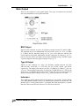
BNC Output
Type-N Output
Indicators
Modulation Modes
Parameter Selection and Adjustment
Display Navigation
Numeric Entry and Secondary Parameters
Stepping Up and Down
Step Size
Store and Recall Settings
Secondary Functions
Cancel
Power and Status
Status Indicators
REF / SYNTH
INTERFACE
POWER
Rear-Panel Overview
AC Power
Timebase
10 MHz IN
10 MHz OUT
Remote Interfaces
GPIB
RS-232
Ethernet
Modulation
IN
Stanford Research Systems
3
4
4
5
5
5
5
6
7
7
8
8
9
9
10
11
11
11
11
11
12
13
13
13
13
13
14
14
14
14
14
14
SG380 Series RF Signal Generators
Table of Contents
OUT
Rear-Panel Optional Outputs
Option 1: Clock Outputs
Option 2: 8 GHz Frequency Doubler
Option 3: I/Q Modulator
14
15
15
15
15
Operation
17
Introduction
Power-On
Setting Parameters
Frequency
Phase
Rel Phase
Amplitude and Power
DC Offset
RF ON/RF OFF
Modulation and Sweeps
Introduction
Modulation Section
Modulation On/Off
Modulation Type
Modulation Function
Modulation Rate
Modulation Deviation
Modulation Waveform Generator, Inputs and Outputs
Linear Modulation
Pulse Modulation
Linear Noise Modulation
Pulse Noise Modulation
Modulation Output
Amplitude Modulation
Setting up Amplitude Modulation:
Amplitude Modulation Example
Frequency Modulation
Setting up Frequency Modulation:
Frequency Modulation Example
Phase Modulation
Setting up Phase Modulation:
Phase Modulation Example
Pulse and Blank Modulation
Setting up Pulse Modulation:
Pulse Modulation Example
Phase Continuous Frequency Sweeps
Setting up Frequency Sweeps:
I/Q Modulation (Option 3)
Setting up External IQ Modulation:
Setting up Internal Noise IQ Modulation:
IQ Noise Modulation Example
17
17
17
18
18
19
20
21
22
23
23
24
24
24
24
25
25
26
26
26
27
27
27
28
28
29
29
31
32
33
33
34
35
35
36
38
39
40
41
42
42
Secondary (Shift) Parameters
43
Stanford Research Systems
ii
SG380 Series RF Signal Generators
Table of Contents
REL Φ=0
PRBS
STEP SIZE
Timebase
NET
TCP/IP Configuration Methods
TCP/IP Based Remote Interfaces
Link Speed
Reset the TCP/IP Interface
GPIB
GPIB Address
Reset the GPIB Interface
RS-232
RS-232 Configuration
Reset the RS-232 Interface
DATA
STATUS
TCP/IP Status
Error Status
Instrument Status
Self Test
LOCAL
INIT
CAL
43
43
43
44
44
45
45
45
45
46
46
46
47
47
47
47
48
48
48
49
49
49
49
49
Factory Default Settings
50
Remote Programming
53
Introduction
Interface Configuration
GPIB
RS-232
LAN
Network Security
Front-Panel Indicators
Command Syntax
Parameter Conventions
Numeric Conventions
Abridged Index of Commands
53
53
54
54
54
55
56
56
57
57
58
Detailed Command List
Common IEEE-488.2 Commands
Status and Display Commands
Signal Synthesis Commands
Modulation Commands
List Commands
Interface Commands
Status Byte Definitions
Serial Poll Status Byte
Standard Event Status Register
60
60
63
65
68
74
76
78
78
79
Stanford Research Systems
iii
SG380 Series RF Signal Generators
Table of Contents
Instrument Status Register
List Mode
List Instrument States
Enables/Disables
Modulation List States
Examples
79
80
80
81
82
83
Error Codes
Execution Errors
Query Errors
Device Dependent Errors
Parsing Errors
Communication Errors
Other Errors
84
84
85
85
86
87
87
Example Programming Code
88
SG380 Series Operation Verification
Overview
Equipment Required
SG380 Series Self Test
93
93
93
94
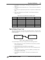
Output Power Tests
BNC Output Power Test
Type-N Output Power Test
Frequency Synthesis Tests
Frequency Generation Tests
Modulation Output Test
Modulation Input Test
Timebase Calibration
SR620 Configuration
Timebase Calibration Test
Calibration
Option Board Verifications
Option 1: Clock Output Test
Option 2: RF Doubler Test
Option 2: DAC Output Test
Option 3: IQ Modulation
94
94
95
97
97
98
99
100
101
101
102
102
102
104
105
106
Conclusions
106
Circuit Description
107
Overview
Block Diagram
Detailed Circuit Description
107
108
110
Front-Panel Display
110
Front-Panel Display EMI Filter
111
Motherboard
Timebases
LF DDS and 19 MHz Reference
111
111
112
Stanford Research Systems
iv
SG380 Series RF Signal Generators
Table of Contents
Microcontroller and Interface
Modulation Processor
Modulation ADC and DACs
RF DDS
RF Block and Rear-Panel Options Interface
Power Conditioning
v
113
114
115
116
117
118
Motherboard to RF Block Jumper
RF Output Block
RF Synthesizer
RF Dividers and Selectors
RF I/Q Modulator, Amplifiers and Attenuators
RF Output Attenuators
BNC Output
Power Supply
118
118
119
120
121
122
122
123
Rear-Panel Options
Clock Output (Options 1)
RF Doubler (Option 2)
I/Q Modulator (Option 3)
Timebase Options
124
124
125
126
126
Appendix A : Rational Approximation Synthesis 127
Phase Lock Loop Frequency Synthesizers
Phase Noise
Increasing Frequency Resolution
A Note on Fractional-N Synthesis
About YIG Oscillators
A New Approach
An Example
Elimination of Error
Conclusion
127
128
129
129
129
130
131
132
132
Appendix B : Parts List
133
Appendix C : Schematic Diagrams
153
Revisions
183
Stanford Research Systems
SG380 Series RF Signal Generators
Safety and Preperation of Use
vii
Safety and Preparation for Use
Line Voltage
The instruments operate from a 90 to 132 VAC or 175 to 264 VAC power source having a
line frequency between 47 and 63 Hz. Power consumption is less than 90 VA total. In
standby mode, power is turned off to the main board. However, power is maintained at all
times to the installed timebase. Units with the standard ovenized quartz oscillator or the
optional rubidium timebase will consume less than 15 VA and 25 VA, respectively, in
standby mode.
Power Entry Module
A power entry module, labeled AC POWER on the back panel of the instrument,
provides connection to the power source and to a protective ground.
Power Cord
The unit is shipped with a detachable, three-wire power cord for connection to the power
source and protective ground.
The exposed metal parts of the box are connected to the power ground to protect against
electrical shock. Always use an outlet which has a properly connected protective ground.
Consult with an electrician if necessary.
Grounding
BNC shields are connected to the chassis ground and the AC power source ground via the
power cord. Do not apply any voltage to the shield.
Line Fuse
The line fuse is internal to the instrument and may not be serviced by the user.
Operate Only with Covers in Place
To avoid personal injury, do not remove the product covers or panels. Do not operate the
product without all covers and panels in place.
Serviceable Parts
There are no user serviceable parts. Refer service to a qualified technician.
Stanford Research Systems
SG380 Series RF Signal Generators
Safety and Preperation of Use
viii
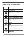
Symbols You May Find on SRS Products
Symbol
Description
Alternating Current
Caution – risk of electrical shock
Frame or Chassis terminal
Caution – refer to accompanying document
Earth (ground) terminal
Battery
Fuse
Power On
Power Off
Power Standby
Stanford Research Systems
SG380 Series RF Signal Generators
Specifications
ix
Specifications
Frequency Setting (fC)
Frequency ranges
BNC output
Type-N output
SG382
SG384
SG386
SMA rear-panel (Opt 2)
SG384
SG386
Frequency resolution
Switching speed
Frequency error
Frequency stability
DC to 62.5 MHz
950 kHz to 2.025 GHz
950 kHz to 4.050 GHz
950 kHz to 6.075 GHz
4.050 GHz to 8.100 GHz
6.075 GHz to 8.100 GHz
1 µHz at any frequency
<8 ms (to within 1 ppm)
<(10–18 + timebase error) × fC
<1:10–11 (1 second Allan variance)
Front-Panel Type-N Output (50 Ω load)
Frequency range
SG382
SG384
SG386
Output power
SG382
SG384
SG386
Power resolution
Power accuracy
Output coupling
User load
VSWR
Reverse protection
950 kHz to 2.025 GHz
950 kHz to 4.050 GHz
950 kHz to 6.075 GHz
+16.5 dBm to –110 dBm (1.5 VRMS to 0.7 µVRMS )
+16.5 dBm (–3.50 dB/GHz above 3 GHz) to –110 dBm
+16.5 dBm (–3.25 dB/GHz above 4 GHz) to –110 dBm
0.01 dBm
1 dB (±2 dB above 4 GHz and above +5 dBm)
50 Ω, AC
50 Ω
<1.6
30 VDC, +25 dBm RF
Front-Panel BNC Output (50 Ω load)
Frequency range
Amplitude
Full specs
Derated specs
Offset
Maximum excursion
Amplitude resolution
Amplitude accuracy
Offset resolution
Harmonics
Spurious
Output coupling
User load
Reverse protection
Stanford Research Systems
DC to 62.5 MHz
1.00 to 0.001 VRMS (+13 dBm to –47 dBm)
1.00 to 1.25 VRMS (+14.96 dBm)
1.50 VDC
1.817 V (amplitude + offset)
<1 %
5 %
5 mV
<–40 dBc
<–75 dBc
DC, 50 Ω 2 %
50 Ω
5 VDC
SG380 Series RF Signal Generators
Specifications
Spectral Purity of the RF Output Referenced to 1 GHz
x
(1)
Sub harmonics
None (No doublers are used below 4 GHz.)
Harmonics
<–25 dBc with <+7 dBm on Type-N output
Spurious
Within 10 kHz of carrier
<–65 dBc
More than 10 kHz from carrier <–75 dBc
Phase noise
Offset from carrier
Phase Noise (typical)
10 Hz
–80 dBc/Hz
1 kHz
–102 dBc/Hz
20 kHz
SG382 & SG384
–116 dBc/Hz
SG386
–114 dBc/Hz
1 MHz
SG382 & SG384
–130 dBc/Hz
SG386
–124 dBc/Hz
Residual FM
1 Hz rms, typical, over 300 Hz to 3 kHz bandwidth
Residual AM
0.006 % rms, typical, over 300 Hz to 3 kHz bandwidth
(1)
Spurs, phase noise and residual FM scale by 6 dB/octave to other carrier frequencies
Phase Setting of Front-Panel Outputs
Phase range
Phase resolution
DC to 100 MHz
100 MHz to 1 GHz
1 GHz to 8.1 GHz
360 °
0.01°
0.1°
1.0°
Internal Modulation Source
Waveforms
Sine THD
Ramp linearity
Rate
SG382 & SG384
fC ≤ 62.5 MHz
fC > 62.5 MHz
SG386
fC ≤ 93.75 MHz
fC > 93.75 MHz
Rate resolution
Rate error
Noise function
Noise bandwidth
Pulse generator period
Pulse generator width
Pulse timing resolution
Pulse noise function
Stanford Research Systems
Sine, ramp, saw, square, pulse, noise
–80 dBc (typical at 20 kHz)
<0.05 % (1 kHz)
1 µHz to 500 kHz
1 µHz to 50 kHz
1 µHz to 500 kHz
1 µHz to 50 kHz
1 µHz
<1:231 + timebase error
White Gaussian noise, RMS = DEV / 5
1 µHz < ENBW < 50 kHz
1 µs to 10 s
100 ns to 9999.9999 ms
5 ns
PRBS length 25 to 219. Bit period (100 + n∙5) ns
100 ns to 10 s in 5 ns steps
SG380 Series RF Signal Generators
Specifications
xi
Modulation Waveform Output
Output impedance
User load
AM, FM, ΦM
Pulse/Blank
Connector
50 Ω (for reverse termination)
Unterminated 50 Ω coax
1 V for full deviation
“Low” = 0 V, “High” = 3.3 VDC
Rear-panel BNC
External Modulation Input
Modes
Unmodulated level
AM, FM, ΦM
Modulation bandwidth
Modulation distortion
Input impedance
Input Coupling
Input offset
Pulse/Blank threshold
Connector
AM, FM, ΦM, Pulse and Blank
0 V input for unmodulated carrier
1 V input for full deviation
>100 kHz
<–60 dB
100 kΩ
AC (4 Hz high pass) or DC
<500 µV
+1 VDC
Rear-panel BNC
Frequency Modulation
Frequency deviation
Minimum
0.1 Hz
Maximum
SG382 & SG384
fC 62.5 MHz:
62.5 MHz < fC 126.5625 MHz
126.5625 MHz < fC 253.1250 MHz
253.1250 MHz < fC 506.25 MHz
506.25 MHz < fC 1.0125 GHz
1.0125 GHz < fC 2.025 GHz
2.025 GHz < fC 4.050 GHz (SG384)
4.050 GHz < fC 8.100 GHz (Opt 2)
SG386
fC 93.75 MHz:
93.75 MHz < fC 189.84375 MHz
189.84375 MHz < fC 379.6875 MHz
379.6875 MHz < fC 759.375 MHz
759.375 MHz < fC 1.51875 GHz
1.51875 GHz < fC 3.0375 GHz
3.0375 GHz < fC 6.075 GHz
6.075 GHz < fC 8.100 GHz (Opt 2)
Stanford Research Systems
Smaller of fC or (64 MHz – fC)
1 MHz
2 MHz
4 MHz
8 MHz
16 MHz
32 MHz
64 MHz
Smaller of fC or (96 MHz – fC)
1 MHz
2 MHz
4 MHz
8 MHz
16 MHz
32 MHz
64 MHz
SG380 Series RF Signal Generators
Specifications
xii
Frequency Modulation (continued)
Deviation resolution
Deviation accuracy
SG382 & SG384
fC 62.5 MHz
fC > 62.5 MHz
SG386
fC 93.75 MHz
fc > 93.75 MHz
Modulation source
Modulation distortion
Ext FM carrier offset
Modulation bandwidth
SG382 & SG384
fC ≤ 62.5 MHz
fC > 62.5 MHZ
SG386
fC ≤ 93.75 MHz
fC > 93.75 MHZ
0.1 Hz
<0.1 %
<3 %
<0.1 %
<3 %
Internal or external
<–60 dB (fC = 100 MHz, fM = 1 kHz, fD = 1 kHz)
<1:1000 of deviation
500 kHz
100 kHz
500 kHz
100 kHz
Phase Continuous Frequency Sweeps
Frequency span
Sweep ranges
SG382 & SG384
0.1 Hz to entire sweep range
DC to 64 MHz
59.375 to 128.125 MHz
118.75 to 256.25 MHz
237.5 to 512.5 MHz
475 to 1025 MHz
950 to 2050 MHz
1900 to 4100 MHz
(SG384)
3800 to 8200 MHz
(Opt. 2 only)
SG386
Deviation resolution
Sweep source
Sweep distortion
Sweep offset
Sweep function
Stanford Research Systems
DC to 96 MHz
89.0625 to 192.1875 MHz
178.125 to 384.375 MHz
356.25 to 768.75 MHz
712.5 to 1537.5 MHz
1425 to 3075 MHz
2850 to 6150 MHz
5950 to 8150 MHz
(Opt. 2 only)
0.1 Hz
Internal or external
<0.1 Hz + (deviation / 1000)
<1:1000 of deviation
Triangle, ramps, or sine up to 120 Hz
SG380 Series RF Signal Generators
Specifications
xiii
Phase Modulation
Deviation
Deviation resolution
DC < fC ≤ 100 MHz
100 MHz < fC ≤ 1 GHz
fC > 1 GHz
Deviation accuracy
SG382 & SG384
fC ≤ 62.5 MHz
fC > 62.5 MHZ
SG386
fC ≤ 93.75 MHz
fC > 93.75 MHZ
Modulation source
Modulation distortion
Modulation bandwidth
SG382 & SG384
fC ≤ 62.5 MHz
fC > 62.5 MHz
SG386
fC ≤ 93.75 MHz
fC > 93.75 MHz
0 to 360°
0.01°
0.1°
1.0°
<0.1 %
<3 %
<0.1 %
<3 %
Internal or external
<–60 dB (fC = 100 MHz, fM = 1 kHz, ΦD = 50°)
500 kHz
100 kHz
500 kHz
100 kHz
Amplitude Modulation
Range
0 to 100 % (Decreases above +7 dBm output)
Resolution
0.1 %
Modulation source
Internal or external
Modulation distortion (fM = 1 kHz, Depth = 50%)
fC 62.5 MHz, BNC output
<1 %
fC > 62.5 MHz, Type-N output <3 % typical
Modulation bandwidth
>100 kHz
Pulse/Blank Modulation
Pulse mode
Blank mode
On/Off ratio
BNC output
Type-N output
fC <1 GHz
1 GHz ≤ fC < 4 GHz
fC ≥ 4GHz
Pulse feed-through
Turn on/off delay
RF rise/fall time
Modulation source
Stanford Research Systems
Logic “high” turns BNC and RF on
Logic “high” turns BNC and RF off
70 dB
57 dB
40 dB
35 dB
10 % of carrier for 20 ns at turn-on (typical)
60 ns
20 ns
Internal or external pulse
SG380 Series RF Signal Generators
Specifications
xiv
External I/Q Modulation (Option 3)
Modulated output
Frequency Range
I/Q inputs
I or Q input offset
I/Q full scale
Carrier suppression
Modulation bandwidth
Front-panel Type-N only (+10 dBm max)
Carrier frequencies above 400 MHz
50 Ω, ±0.5 V, (rear BNCs)
<500 µV
(I2 + Q2)1/2 = 0.5 V
>40 dBc (>35 dBc above 4 GHz)
200 MHz
Square Wave Clock Outputs (Option 1)
Differential clocks
Frequency range
Transition time
Jitter (fC> 62.5 MHz)
Jitter (fC 62.5 MHz)
Amplitude
Offset
Amplitude & Offset resolution
Amplitude & Offset accuracy
Output coupling
Compliance
Rear-panel SMAs drive 50 Ω loads
DC to 4.05 GHz
<35 ps (20 % to 80 %)
300 fs rms (typical, 1 kHz to 5 MHz BW at 1 GHz)
<10-4 U.I. (1 kHz to 5 MHz or fc/2 BW)
0.4 to 1.0 VPP
2 VDC
5 mV
5 %
DC, 50 Ω 2 %
ECL, PECL, RSECL, CML & LVDS
RF Doubler Output (Option 2)
Output
Frequency range (SG384)
Frequency range (SG386)
RF amplitude
4.05 to 7 GHz
7 to 8.10 GHz
Overrange
Sub harmonic (fC / 2)
fC < 6.5 GHz
fC = 8.1 GHz
Mixing products (2fC and 3fC / 2)
Harmonics (n × fC)
Spurious (8 GHz)
Phase noise (8 GHz)
Amplitude resolution
Amplitude accuracy
4.05 to 6.5 GHz
6.5 to 8.10 GHz
Modulation modes
Output coupling
Reverse protection
Stanford Research Systems
Rear-panel SMA
4.050 to 8.10 GHz
6.075 to 8.10 GHz
–10 dBm to +13 dBm
–10 dBm to +7 dBm
+16.5 dBm
<–25 dBc typical
<–12 dBc typical
<–20 dBc
<–25 dBc
<–55 dBc ( > 10 kHz offset)
–98 dBc/Hz at 20 kHz offset, typical
0.01 dBm
1 dB
2 dB
FM, ΦM, and Sweeps
AC, 50 Ω
30 VDC, +25 dBm RF
SG380 Series RF Signal Generators
Specifications
xv
DC Bias Source (comes with Option 2)
Output
Voltage range
Offset voltage
DC accuracy
DC resolution
Output resistance
Current limit
Rear-panel SMA
10 V
<20 mV
0.2 %
5 mV
50 Ω
20 mA
Timebase Input
Frequency
Amplitude
Input impedance
10 MHz, 2 ppm
0.5 to 4 VPP (–2 dBm to +16 dBm)
50 Ω, AC coupled
Timebase Output
Frequency
Source
Amplitude
10 MHz, sine
50 Ω, DC transformer coupled
1.75 VPP 10 % (8.8 1 dBm)
Standard OCXO Timebase
Oscillator type
Stability
Aging
Oven controlled, 3rd OT, SC-cut crystal
<0.002 ppm (0 to 45°C)
<0.05 ppm/year
Rubidium Timebase (Option 4)
Oscillator type
Physics package
Stability
Aging
Oven controlled, 3rd OT, SC-cut crystal
Rubidium vapor frequency discriminator
<0.0001 ppm (0 to 45°C)
<0.001 ppm/year
Computer Interfaces (all are standard)
Ethernet (LAN)
GPIB
RS-232
10/100 Base-T. TCP/IP & DHCP default.
IEEE-488.2
4.8k-115.2k baud, RTS/CTS flow
Line power
EMI Compliance
Dimensions
Weight
Warranty
<90 W, 90 to 264 VAC, 47 to 63 Hz with PFC
FCC Part 15 (Class B), CISPR-22 (Class B)
8.5” × 3.5” × 13” (W × H × D)
<10 lbs
One year on parts and labor
General
Stanford Research Systems
SG380 Series RF Signal Generators
Specifications
xvi
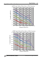
Single Sideband Phase Noise Spectra
SG384 Single Sideband Phase Noise vs Offset Frequency
-60
Phase Noise (dBc/Hz)
-70
-80
-90
-100
4GHz
-110
1GHz
-120
100MHz
-130
10MHz
-140
-150
10
100
1,000
10,000
100,000 1,000,000 10,000,000
Frequency Offset (Hz)
SG386 Single Sideband Phase Noise vs Offset Frequency
-60.0
Phase Noise (dBc/Hz)
-70.0
-80.0
-90.0
-100.0
6GHz
-110.0
1GHz
-120.0
100MHz
-130.0
10MHz
-140.0
-150.0
10
100
1,000
10,000
100,000 1,000,000 10,000,000
Frequency Offset (Hz)
Stanford Research Systems
SG380 Series RF Signal Generators
Specifications
xvii
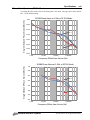
Phase Noise Spectra vs RF PLL Modes
Single Sideband Phase Noise (dBc/Hz)
To change the PLL mode, refer to the front panel CAL menu. See page 49 for more details.
PLL 1 is the default setting.
-90.0
SG384 Phase Noise at 1 GHz vs RF PLL Mode
-100.0
-110.0
RF PLL 1
-120.0
-130.0
-140.0
RF PLL 2
-150.0
-160.0
1,000
10,000
100,000
1,000,000
Single Sideband Phase Noise (dBc/Hz)
Frequency Offset from Carrier (Hz)
-90
SG386 Phase Noise at 1 GHz vs RF PLL Mode
-100
-110
RF PLL 1
-120
-130
-140
RF PLL2
-150
-160
1,000
10,000
100,000
1,000,000
Frequency Offset from Carrier (Hz)
Stanford Research Systems
SG380 Series RF Signal Generators
Typical Operating Characteristics
xviii
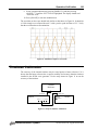
Typical Waveforms
Amplitude Modulation
Waveform 1 is a 20 kHz
carrier
being
amplitude
modulated by a 1 kHz sine
wave. The top trace is the rear
panel Modulation output,
while the bottom trace is the
front-panel BNC output:
Setup:
Frequency
Amplitude BNC
Offset BNC
Modulation
Type
Function
Rate
Depth
ON
20 kHz
1 VPP
0V
AM
Sine
1 kHz
100%
Waveform 1: AM Modulation
FSK (Frequency Shift Keying)
In Waveform 2 the internal modulator is set to FM between 1 MHz and 3 MHz with a
100 kHz square wave. The top trace is the rear panel Modulation output, while the middle and
bottom traces are the front panel BNC and Type-N outputs.
Setup:
Frequency
Amplitude
BNC
Type-N
Modulation
Type
Function
Rate
Deviation
On
2 MHz
1 VPP
2 VPP
FM
Square
100 kHz
1 MHz
Waveform 2: FSK Modulation
Stanford Research Systems
SG380 Series RF Signal Generators
Typical Operating Characteristics
xix
Pulse Modulated Outputs
Waveform 3 is a 50 MHz carrier being pulse modulated with a 1 MHz, 300 ns pulse waveform.
The upper trace is the timing signal with the middle trace being the BNC output, and the lower
trace being the RF output. There are delays of 50 ns in the gating circuitry as shown.
Setup:
Frequency
Amplitude
Type-N
BNC
Modulation
Type
Function
Period
Duty Factor
ON
50 MHz
2 VPP
2 VPP
Pulse
Square
1 µs
30%
Waveform 3: Pulse Modulated Output
Differential Clock Outputs (Option 1)
Waveform 4 shows the optional
rear panel clock outputs with the
frequency set to 100 MHz. The
top trace is front panel Type-N
output with the differential clock
outputs depicted by the lower
traces. The displayed transition
times are limited by the 1.5 GHz
bandwidth of the oscilloscope.
Setup:
Frequency
Amplitude
Type-N
Clock
Offset Clock
Modulation
100 MHz
1 VPP
1 VPP
0V
Off
Waveform 4: Clock Outputs
Stanford Research Systems
SG380 Series RF Signal Generators
Typical Operating Characteristics
xx
Typical Spectra
The following spectra show typical frequency domain performance for the SG380 series signal
generators:
Unmodulated Carrier
Waveform 5 shows a direct measurement taken on a spectrum analyzer with a 200 kHz span and
100 Hz RBW. The noise floor of the spectrum analyzer dominates over most of the 200 kHz
span.
Setup:
Frequency
1 GHz
Amplitude Type-N 0 dBm
Modulation
OFF
Spectrum Analyzer set for:
Center Frequency 1 GHz
Span
200 kHz
Resolution BW
100 Hz
Waveform 5: Unmodulated 1 GHz Output
Frequency Modulation with Modulation Index of 2.40477
Waveform 6 depicts a 50 MHz carrier frequency modulated at a rate of 10 kHz and a deviation of
24.0477 kHz, for a modulation index β = 2.40477. The carrier amplitude is proportional to the
Bessel function J 0 (β) and has its
first zero at 2.40477, and thus
suppresses the carrier.
Setup:
Frequency
Amplitude Type-N
Amplitude BNC
Modulation
Type
Function
Rate
Dev
ON
50 MHz
0 dBm
0 dBm
FM
Sine
10 kHz
24.04 kHz
Waveform 6: 50 MHz with FM Carrier Suppressed
Stanford Research Systems
SG380 Series RF Signal Generators
Typical Operating Characteristics
xxi
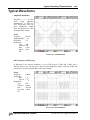
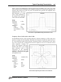
I/Q Modulation (Option 3) by an Internal Noise Source
Option 3 allows I/Q modulation for output frequencies from 400 MHz to 6.075 GHz. Two signal
sources may be used for modulation: the external I & Q inputs or an internal noise generator. The
external I & Q inputs are on the rear panel. The internal noise generator has adjustable noise
bandwidth from 1 Hz to 50
kHz. Waveform 7 is a 1 GHz
carrier being modulated by
the internal noise generator
with 1 kHz noise bandwidth.
Setup:
Frequency
Amplitude
Type-N
Modulation
Type
Function
Dev (ENBW)
ON
1 GHz
–10 dBm
I/Q
Noise
1.0 kHz
Waveform 7: I/Q Modulation using internal noise source
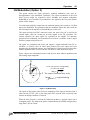
Frequency offset of 1 kHz, 100% AM at 5 kHz
An unmodulated carrier at the spectrum analyzer’s reference frequency (1 GHz in this case)
appears as a single dot in the I/Q plane. When the carrier frequency is offset, the single dot moves
in a circle about the center of the I/Q plane. The pattern shown in Waveform 8 occurs when
the carrier amplitude is modulated with 100 % depth at a rate of five times the carrier
offset frequency (creating five
lobes). The symmetry of the lobes
indicates that there is no residual
phase distortion (AM to ΦM
conversion) in the amplitude
modulator. The narrow line of the
trajectory is indicative of low phase
and amplitude noise.
Setup:
Frequency
Amplitude
Type-N
Modulation
Type
Function
Rate
Depth
ON
1.000001 GHz
0 dBm
AM
Sine
5.0 kHz
100 %
Waveform 8: I/Q Polar plot of offset carrier with AM
Stanford Research Systems
SG380 Series RF Signal Generators
Quick Start Instructions
1
Quick Start Instructions
This is intended to help the first time users get started with the RF Signal Generator and to help verify its
functionality.
Connect the rear panel AC power to the AC mains (90 to 264 VAC, 47 to 63 Hz). Then:
1. Push the power button “in” to turn on the unit.
a. The model number will be briefly displayed
b. Then the firmware version and unit serial number
c. The unit will recall the its last operating state and begin operation
It is important to realize that the SG380 series signal generators resume operating with the same settings
which were active when the unit was last turned off. There is a simple way to preset the instrument to a
default state without changing any of the stored settings or the communications configuration: Notice
that there is a “shifted function” above each key in the NUMERIC ENTRY portion of the key pad. To
initialize the unit to its default settings, in the NUMERIC ENTRY section:
2. Press the [SHIFT] key
a. The SHIFT LED will turn “on”
3. Press the number [0] (whose shifted function is “INIT”)
a. The display shows” init. PrESS EntEr”
4. Press the “ENTER” key (lowest, rightmost key [Hz % dBm])
a. The instrument will be set to its default state
The default setting displays the frequency (10 MHz) and sets the AMPL of the BNC and Type-N outputs
to 0 dBm (1 mW into 50 Ω or 0.63 VPP). Two green LEDs indicate that both the BNC and the Type-N
outputs are active, and another LED shows that the modulation is “OFF”. The “LOCK” LED in the
REF/SYNTH section should be “ON” (as should the “EXT” LED if the unit is connected to an external
10 MHz reference.)
Connect the front panel outputs to an oscilloscope. The oscilloscope timebase should be set for 50 ns/div
and vertical sensitivity 200 mV/div with DC coupling and 50 Ω input impedance. The displayed cycle
period should be 100 ns (2 divisions) and the displayed amplitude should be 630 mVPP. (The displayed
amplitude will be twice that if the oscilloscope input is not set for 50 Ω.)
Here are some things to try:
1.
2.
3.
4.
5.
6.
7.
8.
Change the frequency to 5 MHz by pressing [5] then [MHz VPP]
Press the SELECT [ ] key six times to select the 1 MHz digit
Press the ADJUST [∆] key to increase the frequency
Press the [AMPL] key to display the power at the Type-N output
Press the ADJUST [∆] key to increase the power by 1 dB
Press the [AMPL] key again to display the power at the BNC output
Press the [MHz VPP] key to change the units from dBm to VPP.
Press the ADJUST [∆] key to increase amplitude by 0.100 V
Stanford Research Systems
SG380 Series RF Signal Generators
Introduction
3
Introduction
Feature Overview
The SG380 series of RF Signal Generators consists of three models. Each instrument is
based on a new frequency synthesis technique which provides low phase noise, agile
modulation, fast settling and virtually infinite frequency resolution. (See Appendix A for
details on the Rational Approximation Frequency Synthesis technique.)
Each of the generators has two front panel outputs with overlapping frequency ranges.
The frequency resolution is 1 µHz at all frequencies. The front panel BNC output spans
DC to 62.5 MHz. The BNC output is DC coupled with an adjustable DC offset and
provides sine wave outputs from 1 mVRMS to 1 VRMS.
The front panel Type-N connector provides outputs from 950 kHz to 2.025 GHz (for the
SG382), or 4.050 GHz (for the SG384), or 6.075 GHz (for the SG386). This AC coupled
output can provide power from -110 dBm to +16.5 dBm. A rear panel option extends the
frequency range of the SG384 or SG386 to 8.1 GHz.
The SG380 generators have extensive modulation capabilities. The front panel outputs
can be amplitude, frequency, phase or pulse modulated by internally generated
waveforms (sines, ramps, triangles, pulse and noise) or by external sources. A rear panel
option allows carrier frequencies above 400 MHz to be IQ modulated by external
sources with more than 100 MHz of bandwidth.
The user interface provides single-key access to the most commonly adjusted
synthesizer parameters (frequency, amplitude, phase, modulation rate and modulation
deviation.) In addition, there are three standard communication interfaces (GPIB, RS232 and LAN) which allow for all instrument parameters to be remotely controlled.
To assist in the development of high speed digital devices, a rear panel option provides
differential clock outputs from DC to 4.05 GHz. These SMA outputs have 35 ps
transition times and can be set to standard logic levels including ECL, PECL, RSECL,
CML and LVDS.
The accuracy, stability and low phase noise of the SG380 series is supported by two
outstanding timebases. The standard timebase uses a 3rd overtone, SC-cut ovenized
10 MHz resonator. In addition to its remarkable stability (<0.002 ppm 0° to 45°C), and
low aging (<0.05 ppm/yr), this oscillator is responsible for the low phase noise close to
carrier (-80 dBc/Hz at 10 Hz offset from a 1 GHz carrier) and its short term stability
(1:10-11 1s root Allan variance).
An optional rubidium timebase reduces the frequency aging to <0.001 ppm/yr. This
timebase (a SRS PRS10 rubidium frequency standard) also improves the frequency
stability to <0.0001 ppm over 0° to 45°C.
The 10 MHz output from the internal timebase is made available on a rear panel BNC
connector. The user can also provide a 10 MHz timebase via a rear panel external
timebase input.
Stanford Research Systems
SG380 Series RF Signal Generators
Introduction
4
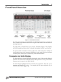
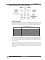
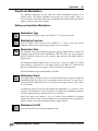
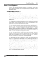
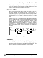
Front-Panel Overview
Figure 1: The SG384 Front Panel
The front panel operation of each SG380 series RF Signal Generator is virtually the
same, with the only substantial difference being the model number and the maximum
operating frequency.
The front panel is divided into seven sections: Parameter Display, Units Display,
OUTPUTS, MODULATION, SELECT/ADJUST, NUMERIC ENTRY, and STATUS.
The power switch is located in the lower right corner of the front panel. Pushing the
switch enables power to the instrument. Pushing the switch again places the instrument
in stand-by mode, where power is enabled only to the internal timebase.
Parameter and Units Display
The front panel has a sixteen digit display showing the value of the currently displayed
parameter. The LEDs below the display indicate which parameter is being viewed. Error
messages may also appear in the display, briefly.
The Units Display highlights the units associated with a parameter. Note that a given
parameter may have multiple views. For example, the RF output amplitude may be
viewed in units of dBm, VRMS, or VPP.
Stanford Research Systems
SG380 Series RF Signal Generators
Introduction
5
Main Output
These are the synthesizer’s main signal outputs. Two types of connectors are provided
due to the bandwidths covered by the instrument.
BNC Output
Signals on this connector are active for frequency settings between DC and 62.5 MHz.
The amplitude may be set independently for levels from 1 mVRMS to 1 VRMS (–47 dBm
to 13 dBm). Increase amplitude setting of 1.25 VRMS (14.96 dBm) are allowed with
relaxed signal specifications. Additionally, the BNC output may be offset by ± 1.5 VDC,
however non-zero offsets will reduce the maximum amplitude setting. The BNC output
is protected against externally applied voltages of up to ± 5 V.
Type-N Output
Signals on this connector are active for frequency settings between 950 kHz
and 2.025 GHz, 4.050 GHz, or 6.075 GHz (for the SG382, SG384 and SG386
respectively). The output power may be set from −110 dBm to 16.5 dBm (0.7 µVRMS to
1.5 VRMS). The maximum output power is reduced by 3.50 dB/GHz above 3 GHz for the
SG384, or by 3.25 dB/GHz above 4 GHz for the SG386. The Type-N output is protected
against externally applied voltages of up to 30 VDC and RF powers up to +25 dBm.
Indicators
Three LEDs are used to indicate which of the outputs are active: BNC, Type-N, and the
4 to 8 GHz (REAR) Doubler. (There is no doubler option available for the SG382). The
Doubler LED is lit only when Option 2 is installed and when the frequency is greater
than 4.05 GHz (for the SG384) or above 6.075 GHz (for the SG386).
Stanford Research Systems
SG380 Series RF Signal Generators
Introduction
6
Modulation Modes
The Modulation section displays the present modulation state and enables the user to
control both the type and function of the modulation.
The [ON/OFF] key enables modulation.
The [MOD TYPE] key allows selection of the type of modulation (via the ADJUST
and keys). The types of modulation available are AM, FM, ΦM, Sweep, and Pulse.
IQ modulation from an internal noise generator, or from external sources, is available as
an option.
The [MOD FCN] key allows the selection of the modulation waveform (via the
ADJUST and keys). The available waveforms include sine, ramp, triangle, square
wave, and noise.
The rear panel external modulation input can also be used in AM, FM, ΦM or Pulse
modulations. When the external source is selected, the signal level is monitored. If the
external source exceeds operational limits the overload LED turns on and remains on
until the condition is removed.
Stanford Research Systems
SG380 Series RF Signal Generators
Introduction
7
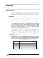
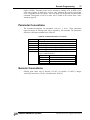
Parameter Selection and Adjustment
Display Navigation
The SELECT/ADJUST section determines which main parameter is shown on the front
panel display. The six basic displays for viewing and modifying instrument settings are
shown in Table 1. Each display is activated by pressing the correspondingly labeled key.
Table 1: Main Parameter Keys
Label
FREQ
PHASE
AMPL
DC OFFS
MOD RATE
MOD DEV
Value Shown in Main Display When Pressed
Frequency (fc)
Phase
Amplitude – sequences through outputs
Offset – sequences through the outputs
Modulation Rate (Pulse Period or ENBW)
Modulation Deviation (Pulse Width or Duty)
For Parameter menus with multiple items, repeatedly pressing the Parameter key allows
cycling through all of its parameters. For example, in the default configuration multiple
key presses of the [AMPL] key will cycle through the various available outputs BNC,
Clock, and Type-N.
Some of the parameters will have a blinking digit (the cursor). The cursor indicates
which digit will be modified when the ADJUST and keys are pressed. The
SELECT and keys allow adjusting the cursor for the desired resolution. The step
size may also set using a shifted function and a numeric entry (to set channel spacing,
for example.)
Stanford Research Systems
SG380 Series RF Signal Generators
Introduction
8
Numeric Entry and Secondary Parameters
This section is used for changing the currently displayed numeric parameter directly. A
parameter is entered numerically and completed by pressing any of the unit keys.
Corrections can be made using the BACK SPACE or the entire entry may be aborted by
pressing the CANCEL key.
For example, to set the frequency to 1.0001 GHz, press the [FREQ] key followed by the
key sequence of [ 1 ] [ ● ] [ 0 ] [ 0 ] [ 0 ] [ 1 ] [GHz].
This section also allows access to secondary (or “Shifted”) functions. The secondary
functions are listed above the key in light blue text. A secondary function is accessed by
first pressing the SHIFT key (indicated by the SHIFT LED being on) followed by
pressing the desired secondary function key.
For example, to set the incremental value for frequency to 12 kHz press [FREQ]
[SHIFT] [9 (STEP SIZE)], followed by the sequence [ 1 ] [ 2 ] [kHz].
Numeric or SHIFT entries may be CANCELed at any time by pressing the SHIFT key.
Stepping Up and Down
Most instrument settings can be stepped up or down by a programmed amount. The
blinking digit identifies the current cursor position and step size. The cursor shows the
digit that will change if the parameter is incremented or decremented via the ADJUST
keys. Pressing the ADJUST () key causes the displayed parameter to increment
(decrement).
Stanford Research Systems
SG380 Series RF Signal Generators
Introduction
9
Step Size
Pressing the ADJUST and keys increments or decrements the value of the selected
digit on the numeric display (to change the selected digit use the SELECT and
keys). To view the step size use SHIFT [ 9 ] (STEP SIZE).
The step size can be changed using the numeric keypad followed by the appropriate unit.
To set the step size to an arbitrary value use SHIFT [ 9 ] and enter the desired step size
followed by the appropriate unit type. For example, to change the frequency’s step size
to 1.25 MHz, first press [Shift] then [ 9 ] followed by 1.25 and finally the [MHz] unit
key. When the cursor is changed to another digit (using the SELECT or keys) the
step size returns to its default value.
Store and Recall Settings
The [STO] and [RCL] keys are for storing and recalling instrument settings,
respectively. Instrument settings include modulation configuration and all associated
step sizes. Up to nine different instrument settings may be stored in the locations 1 to 9.
To save the current settings to location 5, press the keys [STO], [5], [ENTER],
sequentially. To recall instrument settings from location 5, press the keys [RCL], [5],
[ENTER] sequentially. Note: the INIT key is used to recall default instrument settings.
See Default Factory Settings in the Operations chapter for additional details.
Stanford Research Systems
SG380 Series RF Signal Generators
Introduction
10
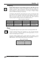
Secondary Functions
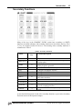
Many of the keys in the NUMERIC ENTRY section have secondary (or SHIFT)
functions associated with them. The secondary functions are listed above the keys. The [
5 ] key, for example, has RS-232 above it. The meaning of the secondary functions is
summarized in Table 2.
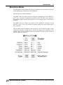
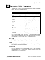
Table 2: Secondary Functions
Label
Primary
Key
CAL
+/-
REL Φ =0
7
PRBS
8
STEP SIZE
NET
GPIB
RS-232
9
DATA
6
INIT
TIMEBASE
0
1
STATUS
2
LOCAL
3
●
4
5
Function Description
Adjust the timebase, and selects the PLL filter mode
Defines the current phase to be 0 degrees and
displays phase
Allows access to the length of the Pseudo-Random
Binary Sequence generator
Set the incremental value used by the ADJUST keys
Configure the Ethernet interface
Configure the GPIB interface
Configure the RS-232 interface
Display the most recent data received over any of
the remote interfaces
Load default instrument settings
Displays the installed timebase and its status
View TCP/IP (Ethernet), error, or instrument status,
as well as running Self-Test
Go to local. Enables front panel keys if in remote
mode.
A more detailed description of each of the secondary functions is given in the Secondary
Functions section of the Operation chapter.
Stanford Research Systems
SG380 Series RF Signal Generators
Introduction
11
The secondary functions can only be accessed when the shift mode is active, which is
indicated by SHIFT LED in the main display. The SHIFT mode can be toggled on and
off by pressing the [SHIFT] key. For example, to configure the PRBS length, press
[SHIFT] [ 8 ] to access the PRBS secondary function.
For menu items with multi-parameter settings, the SELECT and keys allow
selection of the various menu items. The ADJUST and keys may be used to
modify a parameter. For example, the first option in the NET menu is TCPIP
ENABLE/DISABLE. Use the ADJUST and keys to change the setting as desired.
Then press SELECT to move to the next option which is DHCP ENABLE/DISABLE.
Continue pressing the SELECT until all TCPIP settings have been configured as
desired.
Cancel
The [SHIFT] key also functions as a general purpose CANCEL key. Any numeric entry,
which has not been completed, can be canceled by pressing the [SHIFT] key. Because of
the dual role played by the SHIFT key, the user may have to press [SHIFT] twice to
reactivate SHIFT mode. The first key press cancels the current action, and the second
key press re-activates SHIFT mode.
Power and Status
The Power and Status section encompass the power switch and displays the status of the
timebase and remote interface(s):
Status Indicators
REF / SYNTH
In the upper right portion of the front panel are two groups of LED
indicators. The upper group is labeled REF / SYNTH and indicates
the status of the internal timebase. The EXT LED indicates that the
instrument has detected an external 10 MHz reference at the
timebase input BNC on the rear panel. If detected, the instrument
will attempt to lock its internal clock to the external reference.
The LOCK LED indicates that unit has locked its internal
frequency synthesizer at the requested frequency. Normally this
LED will only extinguish momentarily when the frequency changes
or an external timebase is first applied to the rear input. If the LED
stays off, it indicates that the signal generator may be unable to lock
to the external timebase. This is most commonly caused by the
external frequency being offset by more than 2 ppm from 10 MHz.
INTERFACE
The lower group of LED indicators is labeled INTERFACE. These LEDs indicate the
current status of any active remote programming interface (Ethernet, RS-232, or GPIB).
The REM (remote) LED turns on when the unit is placed in remote mode by one of the
remote interfaces. In this mode, all the front panel keys are disabled and the instrument
Stanford Research Systems
SG380 Series RF Signal Generators
Introduction
12
can only be controlled via the remote interface. The user can return to normal, local
mode by pressing the [3] key (also labeled [LOCAL]). The ACT (activity) LED flashes
when a character is received or sent over one of the interfaces. This is helpful when
troubleshooting communication problems. If a command received over the remote
interface fails to execute due to either a parsing error or an execution error, the ERR
(error) LED will turn on. Information about the error is available in the STATUS
secondary display.
POWER
The power switch has two positions: STANDBY (button out) and ON (button in).
In STANDBY mode, power is only supplied to the internal timebase and the power
consumption will not exceed 25 watts. In ON mode, power is supplied to all circuitry but
the power consumption will not exceed 90 watts.
Stanford Research Systems
SG380 Series RF Signal Generators
Introduction
13
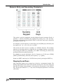
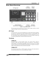
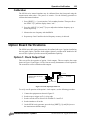
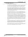
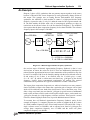
Rear-Panel Overview
Figure 2: The SG384 Rear Panel
The rear panel provides connectors for AC power, remote computer interfaces, external
frequency references, and various additional options.
AC Power
Connect the unit to a power source through the power cord provided with the instrument.
The center pin is connected to the chassis so that the entire box is earth grounded. The
unit will operate with an AC input from 90 to 264 V, and with a frequency of 47 to 63
Hz. The instrument requires 90W and implements power factor correction. Connect only
to a properly grounded outlet. Consult an electrician if necessary.
Timebase
10 MHz IN
This input accepts an external 10 MHz reference. The external reference should be
accurate to at least 2 ppm, and provide a signal of no less than 0.5 VPP while driving a
50 Ω impedance. The instrument automatically detects the presence of an external
reference, asserting the front panel EXT LED, and locking to it if possible. If the unit is
unable to lock to the reference, the LOCK LED is turned off.
10 MHz OUT
The instrument also provides a 10 MHz output for referencing other instrumentation to
the internal high stability OCXO or optional Rubidium Timebase.
Stanford Research Systems
SG380 Series RF Signal Generators
Introduction
14
Remote Interfaces
The instruments support remote control via GPIB, RS-232, or Ethernet. A computer can
perform any operation that is accessible from the front panel. Programming the
instrument is discussed in the Remote Programming chapter. Please refer to the
respective Remote Programming Configuration section before attempting to
communicate with the signal generators via any computer interface.
GPIB
The signal generators have a GPIB (IEEE-488) communications port for
communications over a GPIB bus. The instruments support the IEEE-488.1 (1978)
interface standard. It also supports the required common commands of the IEEE-488.2
(1987) standard.
RS-232
The RS-232 port uses a standard 9 pin, female, subminiature-D connector. It is
configured as a DCE and supports baud rates from 4.8 kb/s to 115 kb/s. The remaining
communication parameters are fixed at 8 Data bits, 1 Stop bit, No Parity, with RTS/CTS
configured to support Hardware Flow Control.
Ethernet
The Ethernet uses a standard RJ-45 connector to connect to a local area network (LAN)
using standard Category-5 or Category-6 cable. It supports both 10 and 100 Base-T
Ethernet connection and a variety of TCP/IP configuration methods.
Modulation
IN
External modulation is applied to this input. The input impedance is 100 kΩ with a
selectable input coupling of either DC or AC (4 Hz roll off).
For analog modulations (AM, FM, M), a signal of ±1 V will produce a full scale
modulation of the output (depth for AM or deviation for FM and M). It supports
bandwidths of 100 kHz and introduces distortions of less than –50 dB.
For Pulse/Blank modulation types, this input is used as a discriminator that has a fixed
threshold of +1 V.
OUT
This output replicates the modulation waveform and has a 50 Ω reverse termination.
When using the internal source for AM, FM, and M, it provides a waveform
determined by the function and rate settings with an amplitude of ±1 VPP into a high
impedance. During external analog modulation, this output mirrors the modulation input.
For Pulse modulation, the output is a 3.3V logic waveform that coincides with the gate
signal.
Stanford Research Systems
SG380 Series RF Signal Generators
Introduction
15
Rear-Panel Optional Outputs
Two rear panel options are available on the SG382: a high speed clock outputs and IQ
modulator inputs for the Type-N output. In addition, a frequency doubler for extending
the frequency output to 8.1 GHz is available for the SG384 and SG386.
Option 1: Clock Outputs
The clock outputs provide a digital representation of the synthesized signal for
frequencies up to 4.05 GHz on a pair of SMA type connectors. The outputs are
differential signals with transition times of 35 ps (20 % to 80 %). They are adjustable for
amplitudes from 0.40 to 1.00 V, offsets of ±2 V, with a resolution of 5 mV. The
amplitude and offsets are set with the front panel AMPL and DC OFFS keys.
For frequencies above 62.5 MHz (93.75 MHz for the SG386), the jitter on the clock
signals will be less than 300 fs with a measurement bandwidth of 5 kHz to 5 MHz. For
frequencies below 62.5 MHz (93.75 MHz for the SG386) the rms jitter will be less than
0.01 % U.I (Unit Interval).
Option 2: 8 GHz Frequency Doubler
This option extends the frequency range to 8.1 GHz with power levels of up to
16.5 dBm. A DC output port is available for providing biasing of external circuits. Both
of these signals use SMA type connectors.
RF OUT
This output is operational for frequencies from 4.05 to 8.1 GHz (on the SG384) or
6.075 GHz to 8.1 GHz (on the SG386). This output is AC coupled and is adjustable over
a range of –10 to +16.5 dBm. The frequency is set with the front panel FREQ key and
the amplitude is set with the front panel AMPL key. The RF output supports FM, ΦM,
and SWEEP modulation.
DC OUT
This output provides DC voltage which is settable over a ± 10 V range with 5 mV of
resolution. Output currents should be limited to ± 20 mA. The output voltage is set via
the front panel DC OFFS key.
Option 3: I/Q Modulator
This option allows I/Q modulation on the front panel Type-N RF output for output
frequencies above 400 MHz. Either an external source or the internal noise source may
be selected via the MOD FCN key in the front panel MODULATION section.
I/Q IN
These inputs accept signals of ±0.5 V, corresponding to full scale modulation, and have
50 Ω input impedances. Both inputs support signal bandwidths from DC to 100 MHz.
I/Q OUT
These outputs duplicate the I/Q modulation waveforms (internally or externally). All I/Q
signals utilize BNC connectors located on the rear panel.
Stanford Research Systems
SG380 Series RF Signal Generators
Operation
17
Operation
Introduction
The previous chapter provided an overview of the instrument’s features. This section
describes the setting of the frequency, phase, amplitude, offset as well as the details of
modulation, storing and recalling setups, and configuration of the computer interfaces.
Power-On
At power on, the unit will briefly display the model number followed by the firmware
version and the unit serial number. When power on initialization has completed, the
instrument will recall the last operational settings from nonvolatile memory.
The instrument continuously monitors front panel key presses and will save the current
instrument settings to nonvolatile memory after approximately five seconds of inactivity.
To prevent the nonvolatile memory from wearing out, the unit will not automatically
save instrument settings that change due to commands executed over the remote
interface. The remote commands *SAV (*RCL) may be used to explicitly save (recall)
instrument settings over the remote interface, if desired. (See the Remote Programming
section for more information about these commands.)
The signal generator can be forced to revert to factory default settings. This is
accomplished by power cycling the unit with the [BACK SPACE] depressed. All
instrument settings, except for the remote interface configurations, will be set back to
their default values. All calibration bytes will be reset to the values set at the most recent
calibration. See the Factory Default Settings section for a list of default settings.
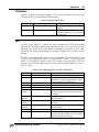
Setting Parameters
The SELECT/ADJUST section determines which parameter is shown in the main front
panel display. The six keys for selecting the display of the main instrument settings are
shown in Table 3. Each display is activated by pressing the corresponding labeled key.
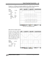
Table 3: Main Display Parameters
SELECT Key
FREQ
PHASE
AMPL
DC OFFS
MOD RATE
MOD DEV
Displayed Value
Frequency (carrier or center frequency if modulating)
Phase of BNC or Type-N outputs
Amplitude or Power – Type-N, BNC, Clock, Doubler
Offset – BNC, Clock, Rear DC Output
Modulation Rate, Pulse Period or noise bandwidth
Modulation Deviation, Pulse Width or Duty Factor
Stanford Research Systems
SG380 Series RF Signal Generators
Operation
18
Frequency
Pressing [FREQ] displays the output frequency and turns on the FREQ LED. The
frequency may be entered in any of the following units: GHz, MHz, kHz, or Hz. For
example, to set the frequency to 5 MHz press the [FREQ] key then press [5] [MHz]. The
frequency resolution is 1 µHz at all frequencies. The units for the displayed frequency
may be changed by pressing the desired unit key. For example, to change the display
from units of MHz to Hz simply press the [Hz] key.
FREQ
The frequency setting determines which outputs may be active at any given time. The
green LED next to the front panel outputs indicate which outputs are enabled. (The
output is also “off” if its amplitude is set below the minimum amplitude for the output.)
None of the outputs operate across the entire frequency range. Table 4 shows the
frequency ranges for each output connector for all models in the series.
Table 4: Frequencies of Operation
Model
Front BNC
Type-N
Rear SMA Clocks
Rear SMA Doubler
SG382
DC-62.5 MHz
950 kHz to 2.025 GHz
DC to 2.025 GHz
Not available
SG384
DC-62.5 MHz
950 kHz to 4.050 GHz
DC to 4.05 GHz
4.05 to 8.10 GHz
SG386
DC-62.5 MHz
950 kHz to 6.075 GHz
DC to 4.05 GHz
6.075 to 8.10 GHz
Phase
Pressing [PHASE] displays the output’s phase and turns on the display PHASE LED.
PHASE
The phase is displayed in degrees and is adjustable over ± 360º. If the phase adjustment
exceeds 360º, the phase is displayed modulo 360º. The displayed phase is set to 0°
whenever the output frequency is changed.
The phase resolution depends upon the current setting of the frequency. For the
frequencies up to 100 MHz the phase resolution is 0.01°, with reduced resolution for
higher frequencies. Table 5 shows the phase resolution verses frequency:
Table 5: Phase Resolution
Frequency Range
Phase Resolution
DC to 100 MHz
0.01°
100 MHz to 1 GHz
0.1°
1 GHz to 8.1 GHz
1.0°
Stanford Research Systems
SG380 Series RF Signal Generators
Operation
19
Rel Phase
In many situations it is useful to be able to define the present phase setting as 0°. The
REL Φ=0 function ([SHIFT] [7] keys) will “REL” the phase display to zero without any
change of the output’s phase.
SHIFT
When you change the phase setting, you change the phase of all outputs from the
synthesizer. This sometimes makes it difficult to see that you have done anything at all.
7
Phase adjustments are usually only made when there are more than one signal source in
a measurement situation. For example, if you have two RF synthesizers, each connected
to the same external 10 MHz timebase and set to the same frequency, you will be able to
see their relative phase by viewing them simultaneously on an oscilloscope or by
applying them both to a mixer and measuring the mixer’s IF output.
You can also see phase changes (for frequencies which are a multiple of 10 MHz) by
viewing the signal on an oscilloscope while triggering the oscilloscope from the rear
panel 10 MHz timebase output.
You can also see the phase adjustment by viewing the RF signal on a polar display of a
vector signal analyzer. (It will be important that the vector signal analyzer and the RF
synthesizer share the same timebase.)
Stanford Research Systems
SG380 Series RF Signal Generators
Operation
20
Amplitude and Power
Pressing [AMPL] displays the output amplitude or power and turns on the “AMPL”
LED.
AMPL
The amplitude has a value for each of the installed outputs, and repeated pressing of
[AMPL] sequences through the amplitude for each output (Type-N, BNC, Clock, and
RF Doubler). Note however, that only those outputs that are active for the current
frequency setting will be accessible. If an output is set below its minimum value it will
be disabled. This is indicated on the display as “off” and by extinguishing the LED
which is next to the output.
All amplitudes (except for clock) may be displayed in units of dBm, VRMS, or VPP, with
clock being restricted to VPP. All stated values assume a load termination of 50 Ω.
Output amplitudes will (approximately) double if not terminated.
The units used for the displayed power or amplitude may be changed with a single key
press. For example, if the Type-N output power is displayed as 0.00 dBm, pressing the
[VRMS] key will display 0.224 VRMS and pressing the [VPP] key will display 0.632 VPP.
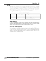
Table 6 lists the range for the various units of the outputs:
Table 6: Output Power Ranges
Output
Power
Front Type-N
Front BNC
(1) (2)
(3)
Rear Doubler
Rear Clocks
(4)
Amplitude (VRMS)
Amplitude (VPP)
-110 dBm → +16.5 dBm 0.707 µ → 1.50 VRMS
2 µ → 4.24 VPP
-47 dBm → +13 dBm
0.001 → 1.000 VRMS
.0028 → 2.82 VPP
-10 dBm → +13 dBm
0.0707 → 1.000 VRMS 0.200 → 2.82 VPP
N.A.
N.A.
0.40 VPP → 1.00 VPP
(1) For the SG384 the maximum power is reduced by 3.50 dB/GHz above 3 GHz. (The
maximum power available at 4 GHz is 13 dBm.)
(2) For the SG386 the maximum power is reduced by 3.25 dB/GHz above 4 GHz. (The
maximum power available at 6 GHz is 10 dBm.)
(3) The AMPL of the BNC may be set as high as 1.25 VRMS (+14.96 dBm), with
reduced distortion specifications, provided that the BNC DC offset is set to 0 V.
(4) The maximum specified power from the rear panel SMA doubler output is reduced
to +7 dBm above 7 GHz. Over range power up to 16.5 dBm may be achieved at
lower frequencies.
Stanford Research Systems
SG380 Series RF Signal Generators
Operation
21
DC Offset
DC
OFFS
Pressing [DC OFFS] displays output offset voltages and turns on the display OFFSET
LED.
On the front panel, only the BNC output has a settable DC offset. The Type-N RF output
is AC coupled and so has no DC offset setting.
There are two rear panel options which also use DC offset settings: The DC offset on the
differential clock outputs (Option 1) and the DC OUT bias source (which is included
with Option 2, the RF doubler).
All three DC offsets are accessed by pressing the [DC OFFS] key repeatedly. The DC
offsets for the front panel BNC, the rear panel differential clock outputs, and the rear
panel DC OUT bias source are always accessible and active (independent of the
frequency setting).
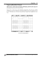
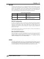
All DC offsets are displayed in VDC. Table 7 gives the DC offset range for the various
outputs:
Table 7: Offset Range
Output
Type-N
BNC
Rear DC Offset
Clock
DC Offset Range
N/A
±1.5V
±10V
±2V
The BNC output will support offsets up to 1.5V. The BNC's output is very linear over
±1.9V while driving a 50 Ω load. To maintain low distortion of AC signals in the
presence of a DC offset it is necessary to reduce the amplitude of the AC signal. The
output provides 13 dBm (2.828 VPP) at no offset, and is reduced linearly to 0 dBm
(0.632 VPP) for offsets of 1.5 V. Table 8 shows the allowed amplitude (or power
settings) for the BNC output for various DC offsets:
Table 8: BNC Output vs. DC Offset
BNC DC Offset
0.00 V
±0.25 V
±0.50 V
±0.75 V
±1.00 V
±1.25 V
±1.50 V
Max Output (VPP)
2.83 VPP
2.46 VPP
2.10 VPP
1.73 VPP
1.37 VPP
0.998 VPP
0.634 VPP
Stanford Research Systems
Max Output (VRMS)
1.00 VRMS
0.871 VRMS
0.741 VRMS
0.612 VRMS
0.483 VRMS
0.353 VRMS
0.224 VRMS
Max Output (dBm)
13.01 dBm
11.81 dBm
10.41 dBm
8.75 dBm
6.69 dBm
3.97 dBm
0.02 dBm
SG380 Series RF Signal Generators
Operation
22
RF ON/RF OFF
SHIFT
These are shifted functions of the [FREQ] and [AMPL] keys, respectively. Press the
[SHIFT] key (which lights the SHIFT LED) followed by the [AMPL] key to turn the RF
“off”, and press the [SHIFT] key followed by the [FREQ] key to turn the RF “on”.
FREQ
The RF ON and RF OFF key presses cause a momentary display of “rf on” / “rf off” on
the main display, and the status LEDs for the outputs are set or cleared accordingly.
SHIFT
The [RF OFF] turns off all RF outputs, while setting the clock output to a static “off”
state (+OUT to “low”, –OUT to “high”). When an output is selected that is “off” the
display will indicate the off status. For example, selecting the Type-N amplitude would
display “ntype off” on the main display.
The [SHIFT] [RF ON] returns all RF outputs to their previously active levels.
AMPL
Stanford Research Systems
SG380 Series RF Signal Generators
Operation
23
Modulation and Sweeps
Introduction
This section describes the instrument’s modulation capabilities. The SG380 series signal
generators have powerful and flexible built-in modulation functions, capable of AM,
FM, ΦM, frequency sweeps, Pulse, and I/Q modulation.
The modulation waveform may be an internally generated sine wave, square wave,
pulse, ramp, triangle, noise, or, may be externally sourced via a rear panel BNC input. A
rear panel BNC connector outputs the modulation waveform with a full scale range of
±1.00 V.
In addition, signal generators with Option 3 have wideband I-Q modulation. The rear
panel BNC I-Q modulation inputs and outputs have >100 MHz bandwidth, ±0.5 V full
scale range, and 50 Ω impedance.
Stanford Research Systems
SG380 Series RF Signal Generators
Operation
24
Modulation Section
This section controls the modulation of the front panel Type-N and BNC outputs and can
provide FM, ΦM, Sweep modulation for the optional rear panel doubler output to
8.10 GHz. The modulation is turned “on” or “off”, and the modulation type (AM, FM,
etc.), and the modulation function (sine, ramp, etc.), are selected in this section.
ON/
OFF
MOD
TYPE
MOD
FNC
Modulation On/Off
The [ON/OFF] key toggles the modulation on/off and the current state is reflected by the
MODULATION ON/OFF LEDs. Make sure that modulation is “OFF” if you want a CW
(unmodulated) output for the signal generator. If the signal generator ever manifests
“unexpected behavior” check the modulation status: Unintentionally enabling the
modulation will give unexpected results.
Modulation Type
The [MOD TYPE] key allows the selection of which type of modulation will be applied
to the synthesizer's output. The ADJUST keys are used to select the desired
modulation type and the current selection is indicated with an LED. The types of
modulation available are AM, FM, ΦM, Sweep, and Pulse. Optional I/Q modulation is
also available if Option 3 is installed.
Modulation Function
The [MOD FCN] key selects one of the various functions used as the modulation
waveform. The ADJUST keys are used to select the desired modulation function.
The current selection is indicated with an LED.
For all modulation types the rear panel external modulation source may be used. When
Option 3 is installed, the I/Q modulation supports separate inputs for the I and Q signals.
Not all modulation types support all modulation functions. Table 9 shows which
modulation types support which functions:
Stanford Research Systems
Noise
External
Square
AM / FM / ΦM
Sweep
Pulse
I/Q (Optional)
Triangle
Type
Ramp
Function
Sine
Table 9: Modulation Type vs. Function
SG380 Series RF Signal Generators
Operation
25
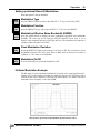
Modulation Rate
MOD
RATE
The [MOD RATE] and [MOD DEV] keys are paired in operation and their parameters
depend upon the current modulation type and function settings.
Pressing [MOD RATE] displays the modulation rate associated with the current
modulation type and turns on either the MOD RATE (for AM/FM/PM and sweep) or the
PERIOD (for pulse/blank) LEDs.
For the standard (AM/FM/ΦM) and sweep modulation types, this parameter is the
frequency of the applied modulation waveform. The allowable range depends on both
the type of modulation and the frequency selected.
For pulse modulation, this selects the period of the pulses which modulate the carrier.
The pulse period is settable in 5ns increments from 1 µs to 10 s.
For I/Q noise modulation (available with Option 3) this key sets the equivalent noise
bandwidth (ENBW) of the internal generated noise source. The ENBW may be set from
1 µHz to 500 kHz.
Modulation Deviation
MOD
DEV
Pressing [MOD DEV] displays the deviation of the current modulation function.
Depending on the modulation type, either the MOD DEV, AM DEPTH, WIDTH, or
DUTY FACTOR is displayed.
During AM modulation, the AM depth is displayed and corresponds to the peak
percentage of the output envelope deviation. For example, if the amplitude is set to 1 VPP
and the AM DEPTH is set for 50%, the amplitude envelope would span from 0.5 V to
1.5 V.
During FM and sweep modulations, the deviation corresponds to the peak frequency
excursion applied to the carrier. For example, if the carrier is set to 1.1 MHz and the
deviation is set to 0.1 MHz, the carrier will span between 1 MHz and 1.2 MHz.
During ΦM modulation, the deviation corresponds to the peak phase excursion applied
to the carrier. For example, if the deviation is set to 10°, then the carrier’s phase
deviation will span ±10°.
During pulse/blank modulation, deviation allows the pulse width or duty factor to be
changed. This parameter may be either a time (“t on” for pulse or “t_off” for blank) or a
duty factor. For example, for a 1 µs pulse period, a width of 500 ns or a duty factor of
50% would be equivalent, and result in the output being on for 50% of the 1 µs period.
Stanford Research Systems
SG380 Series RF Signal Generators
Operation
26
Modulation Waveform Generator, Inputs and Outputs
The instrument’s modulation capabilities include both internal and external modulation
sources. The modulating waveform is replicated on the rear panel Modulation Output
connector.
Linear Modulation
For AM / FM / ΦM, and Sweep, the modulation source can be either the internal
generator or the rear panel external modulation input.
The internal modulation source is capable of generating sine, ramps, triangular, or
square waves, at frequencies of up to 500 kHz. The instrument limits the modulation rate
to 50 kHz for carrier frequencies above 62.5 MHz (93.75 MHz for the SG386).
The rear panel external modulation input supports bandwidths of 500 kHz, but the
modulation bandwidth is limited to 100 kHz for fC greater than 62.5 MHz (93.75 MHz
for the SG386). The sensitivity is set such that a 1 V signal results in a full scale
deviation (depth) in the output. For example: in ΦM, if the deviation is set for 10°,
applying a level of –1 V produces a –10° shift; applying 0 V produces no shift; and
applying +1 V produces a 10° shift.
When modulation is enabled using an internal source, the rear panel modulation output
will provide a waveform of the selected function with a full scale range of ±1 V. When
external modulation is selected the modulation output tracks the applied signal.
Pulse Modulation
There are two modes of pulse modulation: Pulse and Blank. The mode is shown in the
main display and is selected with the ADJUST keys after [MOD TYPE] is
pressed.
In Pulse Mode, the RF signal is turned “on” by the internally generated or externally
applied signal. In Blank Mode, the RF signal is turned “off” by the internally generated
or externally applied signal.
The internal pulse modulation source is a digital waveform whose period and “on” time
is settable from 1 µs to 10 s with 5 ns of adjustability. The period of the digital
waveform is set via the [MOD RATE] key. The “on” time (for Pulse Mode) or “off”
time (for Blank Mode) is set via the [MOD DEV] keys.
When an external input is selected the rear panel external modulation input is set for a
threshold of 1V. The resulting signal is used in place of the internal source.
In Pulse and Blank Modes, the modulation output is a 3.3 V logic signal, which tracks
the pulse waveform.
Stanford Research Systems
SG380 Series RF Signal Generators
Operation
27
Linear Noise Modulation
For AM, FM and ΦM, the noise source is pseudo random additive white Gaussian noise
(AWGN). The bandwidth of the noise is set by the [MOD RATE] and the RMS
deviation is set by the [MOD DEV].
The peak deviation will be about five times the set RMS deviation. This forces limits on
the maximum allowed deviation corresponding to one fifth of the non-noise
counterparts. For example, at a carrier frequency of 500 MHz the maximum FM
deviation for a sine wave function is limited to 4 MHz, and so the maximum deviation
for noise modulation is limited to 800 kHz.
For linear modulation, the rear panel output will provide 200 mV RMS that will be band
limited to the selected modulation rate. Again, the peak deviation will be five times this,
or ±1 VPP.
Pulse Noise Modulation
For pulse modulation, the noise source is a Pseudo Random Bit Sequence (PRBS). The
n
bit period is set by the [MOD RATE]. The PRBS supports bit lengths of 2 , for
5 ≤ n ≤ 19 which correspond to a noise periodicity from 31 to 524287 periods. The bit
length n is set via the [Shift] [PRBS or 8] key.
During pulse PRBS modulation, the rear panel output will be a 3.3 VPP waveform with a
duty factor equal to 2n/2 / 2n-1 (approximately 50 %).
Modulation Output
A rear panel BNC provides a copy of the modulation function with ±1 V full scale
range. This output will be a sine, ramp, triangle, square wave, pulse or noise depending
on the selected internal modulation function.
When an external source is applied to the modulation input it will be bandwidth limited,
digitized, and reproduced at the modulation output. The transfer function has a
bandwidth of about 1 MHz and a latency of about 950 ns.
The modulation output is a useful source even when the RF capabilities of the
instrument are not required. The sine output is exceptionally clean, with a spur-free
dynamic range typically better than -80 dBc. It can be used as a pulse generator with
5 ns timing resolution, or a PRBS generator. It is a very convenient noise source, with
adjustable ENBW from 1 µHz to 500 kHz.
The modulation output has a 50 Ω source impedance (to reverse terminate reflections
from the user’s load) but the output should not be terminated into 50 Ω.
Stanford Research Systems
SG380 Series RF Signal Generators
Operation
28
Amplitude Modulation
The amplitude modulation can use either the internal modulation generator or an
external source. The internal modulator can generate sine, ramp, triangle, square, or
noise waveforms. Amplitude modulation is not applied to the optional rear panel doubler
output or to the rear panel clock outputs.
Setting up Amplitude Modulation:
MOD
TYPE
MOD
FNC
MOD
RATE
Modulation Type
Press the [MOD TYPE] key and use the ADJUST keys to select AM.
Modulation Function
Press the [MOD FCN] key and use the ADJUST keys to select the desired
modulation function (sine, ramp, triangle, square, noise or external).
Modulation Rate
For internally generated modulation functions, pressing [MOD RATE] displays the
modulation rate and turns on the MOD RATE LED. The value may be set using the
SELECT/ADJUST arrow keys or via a numeric entry and one of the [MHz] [kHz] or
[Hz] unit keys.
The internal modulation supports rates of 50 kHz for fC above 62.5 MHz (93.75 MHz
for the SG386) or 500 kHz for fC less than or equal to 62.5 MHz (93.75 MHz for the
SG386). The Modulation rate supports 1 µHz of resolution at all frequencies.
External modulation supports bandwidths of 100 kHz.
MOD
DEV
Modulation Depth
Press [MOD DEV] to display and set the AM modulation depth, which also lights the
AM DEPTH LED. The value may be set using the numeric entry and [ % ] unit keys, or
using the SELECT/ADJUST arrow keys. This value has a range of zero to 100 % with a
0.1 % resolution.
A modulation depth of X percent will modulate the amplitudes by ± X percent. As an
example, if the amplitude is set for 224 mVRMS (0 dBm), with a modulation depth of
50%, the resulting envelope would traverse 112 to 336 mVRMS.
NOTE: The outputs are limited to 1 VRMS (+13 dBm). If the modulation is increased
such that the peak envelope would exceed this limit, the amplitude will be automatically
reduced, and the screen will momentarily display “output reduced”.
ON/
OFF
Modulation On/Off
Press the [ON/OFF] key to turn the modulation “ON”.
Stanford Research Systems
SG380 Series RF Signal Generators
Operation
29
Amplitude Modulation Example
Illustrated below is an example of amplitude modulation. A 20 kHz carrier, with
amplitude of 1 VPP into 50 Ω, is being amplitude modulated by an internally generated
sine wave. The modulation rate is 1 kHz and the modulation depth is 100%.
Two traces are shown below. The upper trace is the 1 kHz modulation waveform (from
the rear panel Modulation Output BNC), offset up two divisions. The lower trace is the
modulated carrier (from the front panel BNC output), offset down one division.
Waveform 9: Amplitude modulation of a 20 kHz carrier
Frequency Modulation
The internal modulation generator or an external source may be used to modulate the
frequency outputs from the front panel BNC, Type-N and (optional) rear panel RF
doubler output. The internal modulator can generate sine, ramp, triangle, square, or
noise waveforms.
During FM, the output frequency traverses fC ± MOD DEV at the specified MOD
RATE. For example, if the frequency is set for 1000 MHz (1 GHz), and the modulation
rate and deviation are set for 10 kHz and 1 MHz, respectively, then the output will
traverse from 1000 MHz, up to 1001 MHz, down to 999 MHz, and back to 1000 MHz at
a rate of 10 kHz (a period of 100 µs).
The FM modulation parameters are dependent upon the frequency setting. Table 10 and
Table 11 list the FM parameters as a function of frequency. All frequency bands span
octaves except for the first band. The internal FM rates correspond to the upper range
that the internal function generator supports. The external bandwidth is defined as the
−3 dB response referenced to the external modulation source. For the bands 2 to 8, the
rates and bandwidths are similar. However, the deviation increases by a factor of two,
from 1 to 64 MHz, for octaves 2 through 8.
Stanford Research Systems
SG380 Series RF Signal Generators
Operation
30
The first band has unique FM capabilities in that it allows setting the deviation of the
carrier frequency to the nearest band edge. If the carrier is set on the upper edge of
62.5 MHz, the deviation is allowed to be set to 1.5 MHz (5 % of fC). This range also
supports a wider internal rate and bandwidth of 500 kHz.
For example, if the frequency is set for 100 kHz, the deviation may be set from zero
to 100 kHz.
Table 10: FM Modulation vs. Frequency for SG382 and SG384
Internal FM
External FM Bandwidth
FM Deviation
Rate. 1 µHz to: DC (or 4 Hz for AC) to:
Smaller of fc
500 kHz
500 kHz
or 64 MHz-fc
Frequency Range
DC 62.5 MHz
62.5 MHz 126.5625 MHz
50 kHz
100 kHz
1 MHz
126.5625 MHz 253.125 MHz
50 kHz
100 kHz
2 MHz
253.125 MHz 506.25 MHz
50 kHz
100 kHz
4 MHz
506.25 MHz 1.0125 GHz
50 kHz
100 kHz
8 MHz
1.0125 GHz 2.025 GHz
50 kHz
100 kHz
16 MHz
2.025 GHz 4.050 GHz (SG384)
50 kHz
100 kHz
32 MHz
4.050 GHz 8.100 GHz (Opt 2)
50 kHz
100 kHz
64 MHz
Table 11: FM Modulation vs. Frequency for SG386
Frequency Range
DC 93.75 MHz
Internal FM
External FM Bandwidth
FM Deviation
Rate. 1 µHz to: DC (or 4 Hz for AC) to:
Smaller of fc
500 kHz
500 kHz
or 96 MHz-fc
93.75 MHz 189.84375 MHz
50 kHz
100 kHz
1 MHz
189.84375 MHz 379.6875 MHz
50 kHz
100 kHz
2 MHz
379.6875 MHz 759.375 MHz
50 kHz
100 kHz
4 MHz
759.375 MHz 1.51875 GHz
50 kHz
100 kHz
8 MHz
1.51875 GHz 3.0375 GHz
50 kHz
100 kHz
16 MHz
3.0375 GHz 6.075 GHz
50 kHz
100 kHz
32 MHz
6.075 GHz 8.100 GHz (Opt 2)
50 kHz
100 kHz
64 MHz
Stanford Research Systems
SG380 Series RF Signal Generators
Operation
31
Setting up Frequency Modulation:
MOD
TYPE
MOD
FNC
MOD
RATE
Modulation Type
Press the [MOD TYPE] key and use the ADJUST keys to select FM.
Modulation Function
Press the [MOD FCN] key and use the ADJUST keys to select the desired
modulation function (sine, ramp, triangle, square, noise or external).
Modulation Rate
Press [MOD RATE] to display the modulation rate. The value may be set using the
SELECT/ADJUST arrow keys or via a numeric entry and one of the [MHz] [kHz] or
[Hz] unit keys.
Internal modulation supports rates of 50 kHz for fC above 62.5 MHz (93.75 MHz for
the SG386) or 500 kHz for fC less than or equal to 62.5 MHz (93.75 MHz for the
SG386), with 1 µHz of resolution.
External modulation supports bandwidths of 100 kHz.
MOD
DEV
Modulation Deviation
Press [MOD DEV] to display and set the FM deviation, which also turns on the
DEVIATION LED. The value may be set using numeric entry and [MHz] [kHz] or [Hz]
unit keys, or the SELECT/ADJUST arrow keys.
The deviation has a range that is dependent on carrier frequency band.
There are seven octaves above the lowest frequency range of DC to 62.5 MHz. The first
octave (62.5 to 125 MHz) supports deviation of 1 MHz, with each succeeding octave
doubling the deviation, thus achieving a 64 MHz of deviation at the 4 to 8 GHz octave
(if the optional doubler is installed.)
NOTE: If the frequency is changed, the deviation may be adjusted as necessary to
maintain limits imposed by the new frequency setting.
ON/
OFF
Modulation On/Off
Press the [ON/OFF] key to turn the modulation “ON”.
Stanford Research Systems
SG380 Series RF Signal Generators
Operation
32
Frequency Modulation Example
Shown below is a 2 MHz carrier being frequency modulated by a 100 kHz square wave with a
1 MHz deviation. In this example of Frequency Shift Keying (FSK) the carrier frequency is
being rapidly switched between 1 MHz and 3 MHz.
The top trace is from the rear panel Modulation Output BNC which shows the 100 kHz
modulating waveform. The middle trace is the front panel BNC output, whose amplitude was set
to 1 VPP. The bottom trace is from the front panel Type-N output, whose amplitude was set to
2 VPP.
Waveform 10: FSK Modulation
Stanford Research Systems
SG380 Series RF Signal Generators
Operation
33
Phase Modulation
The phase modulation can use either the internal modulation generator or an external
source. The internal modulator can generate sine, triangle, ramp, square, or noise
waveforms.
The phase of the output traverses the specified deviation at the modulation rate. For
example, with a frequency of 1000 MHz (1 GHz), and modulation rate and deviation set
to 10 kHz and 45 degrees, respectively, the output will be a fixed frequency with its
phase traversing ±45 degrees at a 10 kHz rate.
The optional rear panel doubler output can also be phase modulated.
Setting up Phase Modulation:
MOD
TYPE
MOD
FNC
MOD
RATE
MOD
DEV
Modulation Type
Press the [MOD TYPE] key and use the ADJUST keys to select ΦM.
Modulation Function
Press the [MOD FCN] key and use the ADJUST keys to select the desired
modulation function (sine, ramp, triangle, square, noise or external).
Modulation Rate
Press [MOD RATE] to display the modulation rate. The value may be set using the
SELECT/ADJUST arrow keys or via a numeric entry and [MHz] [kHz] or [Hz] unit
keys.
Modulation Deviation
Press [MOD DEV] to display and set the M deviation, which turns on the
DEVIATION LED. The value may be set using the numeric entry and the [DEG] unit
key.
The phase deviation resolution depends on the frequency setting. For frequencies below
100 MHz, the phase deviation resolution is 0.01°. For frequencies between 100 MHz and
1 GHz the resolution is reduced to 0.1°, and is 1° for frequencies above 1 GHz.
For frequencies less than or equal to 62.5 MHz (93.75 MHz for the SG386) the accuracy
of the phase deviation is 0.1 %. For frequencies above 62.5 MHz (93.75 MHz for the
SG386) the accuracy is reduced to 3 %.
ON/
OFF
Modulation On/Off
Press the [ON/OFF] key to turn the modulation “ON”.
Stanford Research Systems
SG380 Series RF Signal Generators
Operation
34
Phase Modulation Example
Shown below is the frequency spectrum of a 0 dBm, 50 MHz carrier, being phase
modulated by a 10 kHz sine with a deviation of 137.78°. Here, the modulation
index, β= phase deviation = 137.78° × 2π / 360° = 2.40477 radians. For phase
modulation by a sine, the carrier amplitude is proportional to the Bessel function J 0 (β),
which has its first zero at 2.40477, which suppresses the carrier to below -88 dB.
Waveform 11: Spectrum of Phase Modulated 50 MHz Carrier
Stanford Research Systems
SG380 Series RF Signal Generators
Operation
35
Pulse and Blank Modulation
Pulse modulation includes both pulse and blank modulation of the front panel BNC and
Type-N outputs. Pulse and blank modulation are logical complements of each other—
pulse modulation enables the output when the pulse waveform is “true”, while blank
modulation disables the output. The functions supported are square, noise (Pseudo
Random Binary Sequence — PRBS), and external.
For internal square wave function the instrument has a 32-bit timing generator clocked
by a 200 MHz source. This allows the period to be set from 1 µs to 10 s with 5 ns
resolution. The pulse duration can then be set from 100 ns up to the full period (less
100 ns). The internal generated pulse waveform is available at the rear panel
Modulation Output BNC.
For pulse (blank) modulation, the output is turned on (off) when the source is at logic
“high”. Pulse modulation is not applied to the optional doubler output.
Setting up Pulse Modulation:
MOD
TYPE
MOD
FNC
MOD
RATE
MOD
DEV
ON/
OFF
Modulation Type
Press the [MOD TYPE] key and use the ADJUST keys to select PULSE or
BLANK.
Modulation Function
Press the [MOD FCN] key and use the ADJUST keys to select the desired
modulation function (pulse, noise or external). If external, then CMOS logic levels
applied to the rear panel modulation input control the pulse or blanking of the outputs.
(See details on PRBS modulation below.)
Pulse Period
Press [MOD RATE] to display the pulse modulation period for the internal source. The
value may be set using the SELECT/ADJUST arrow keys or via numeric entry plus one
of the [ns] [µs] [ms] [enter] unit keys.
Pulse Width or Duty Factor
Press [MOD DEV] to display and set the pulse width of the internal source, which also
turns on either the WIDTH or DUTY FACTOR LED. The value may be set using
numeric entry and [ns] [µs] [ms] [enter] or [%] unit keys, or the SELECT/ADJUST
arrow keys.
Modulation On/Off
Press the [ON/OFF] key to turn the modulation “ON”.
Stanford Research Systems
SG380 Series RF Signal Generators
Operation
36
Pulse Modulation Example
The waveforms below show the front panel BNC and Type-N outputs for a pulse
modulated carrier frequency of 50 MHz. The internal pulse modulator was set to 1 µs
period, with a 300 ns “on” time (or a 30% duty cycle).
The output amplitudes were set to 2 VPP into 50 Ω. The top trace is the rear panel
Modulation Output signal. The middle trace is the BNC output. The bottom trace is the
Type-N output. Both traces show about 50 ns latency in their response to the gating
signal. The Type-N output also shows some gate feed-though at the leading edge if the
signal.
Waveform 12: Pulse modulated 50 MHz carrier
Stanford Research Systems
SG380 Series RF Signal Generators
Operation
37
More about PRBS Noise Modulation
When the noise function is selected for pulse modulation, the modulation source is a
pseudo random binary sequence (PRBS) generator. The PRBS is used to gate the
Type-N and BNC outputs.
The period of the PRBS may be set from 100 ns to 10 s, with 5 ns resolution via the
[MOD RATE] key. The default PRBS period is 1 kHz. At the default setting, the RF
output would be set “on” or “off”, randomly, every millisecond.
The default PRBS run length is 9 bits and so the PRBS pattern repeats after 2 9-1 = 511
periods. The PRBS run length can be changed from 5 to 19 bits for repeat cycles
between 31 and 524,287 periods.
To modify the PRBS run length:
SHIFT
Press the [Shift] key followed by the [PBRS(8)] key to display the PRBS run length (in
bits). Press the ADJUST keys or enter a number, N, between 5 and 19 followed
by the ENTER key. The PRBS will repeat after 2N-1 cycles.
8
The PRBS is available at the rear panel Modulation Output BNC. The source is 0 to
3.3 V with 50 Ω source impedance. The output should not be terminated into 50 Ω.
Stanford Research Systems
SG380 Series RF Signal Generators
Operation
38
Phase Continuous Frequency Sweeps
Frequency sweeps allow the traversing of an entire frequency band. The sweep
modulation may use the internal sine, triangle, or ramp waveforms or an external
modulation source. Sweep rates of up to 120 Hz and sweep ranges from 10 Hz up to an
entire frequency band are supported with resolutions of 1 µHz.
Frequency sweeps can require the instrument’s RF VCO to sweep through an entire
octave. For the sweep to be phase continuous the RF VCO PLL must remain in “LOCK”
during the sweep. This is why the maximum sweep rate is limited to 120 Hz and why the
frequency slew rate is internally limited for the ramp function. The slew rate of external
modulation sources should also be limited if a phase continuous sweep is required.
The RF Synthesizers have eight frequency bands as shown in Tables below:
Table 12: Sweep Frequency Bands for the SG382 and SG384
Band
1
2
3
4
5
6
7 (SG384)
8 (Option 2)
Frequency
DC ⇒ 64 MHz
59.375 ⇒ 128.125 MHz
118.75 ⇒ 256.25 MHz
237.5 ⇒ 512.5 MHz
475 ⇒ 1025 MHz
950 ⇒ 2050 MHz
1900 ⇒ 4100 MHz
3800 ⇒ 8200 MHz
Table 13: Sweep Frequency Bands for the SG386
Band
1
2
3
4
5
6
7
8 (Option 2)
Stanford Research Systems
Frequency
DC ⇒ 96 MHz
89.0625 ⇒ 192.1875 MHz
178.125 ⇒ 384.375 MHz
356.25 ⇒ 768.75 MHz
712.5 ⇒ 1537.5 MHz
1425 ⇒ 3075 MHz
2850 ⇒ 6150 MHz
5950 ⇒ 8150 MHz
SG380 Series RF Signal Generators
Operation
39
Setting up Frequency Sweeps:
MOD
TYPE
MOD
FNC
MOD
RATE
MOD
DEV
ON/
OFF
Modulation Type
Press the [MOD TYPE] key and use the ADJUST keys to select SWEEP.
Modulation Function
Press the [MOD FCN] key and use the ADJUST keys to select either sine, ramp,
triangle or external modulation function.
Sweep Rate
Press [MOD RATE] to display the modulation rate. This value may be set using the
SELECT/ADJUST arrow keys or via numeric entry followed by [Hz] unit key. The
Rate may be set from 1 µHz to 120 Hz with a resolution of 1 µHz.
Sweep Deviation
Press [MOD DEV] to display and set to the Sweep deviation. This turns on the
‘DEVIATION’ LED. The value may be set using numeric entry plus one of the hertz
unit keys, or the SELECT/ADJUST arrow keys. The deviation may be set to sweep an
entire band or any part thereof.
Modulation On/Off
Press the [ON/OFF] key to turn the modulation “ON”.
Stanford Research Systems
SG380 Series RF Signal Generators
Operation
40
I/Q Modulation (Option 3)
This option extends the signal generator’s standard modulation suite with Inphase/Quadrature (IQ) modulation capabilities. This allows modulation of the front
panel Type-N output for frequencies above 400 MHz and supports modulation
bandwidths of over 100 MHz. I/Q modulation is not applied to the rear panel doubler
option or BNC outputs.
To avoid output amplifier compression, the maximum output power setting is +10 dBm
during I/Q modulation. This guarantees that the modulator output does not exceed the
full scale output of the amplifier when both I&Q are at full scale.
This option provides four BNC connectors on the rear panel. One pair is used for the
external inputs, while the second pair provides outputs of the I/Q waveforms. For
external operation, the input signals are replicated on the outputs. For internally
generated noise modulation, the baseband noise waveform is available on the I output
with the Q output being held at zero.
The inputs are terminated with 50 Ω, and support a signal bandwidth from DC to
100 MHz. A ±500 mV level on either input produces full scale output (full scale
determined by the amplitude setting). Any combination of I and Q input levels that when
added in quadrature have a level of 500 mV will likewise result in full-scale output.
Figure 3 depicts the relationship between I and Q levels when added in quadrature and
the resulting output magnitude
Q
Circle with 500 mV corresponding
to a full-scale output
Qin
I
Iin
Mag = I 2 + Q 2
The output is instantaneously set by:
Mag
(500mV) • AmplitudeSetting
Figure 3: IQ Relationship
The inputs are designed to allow full-scale modulation. Each input is monitored and if
either exceeds 525 mV (105 %) the front panel EXT overload LED is turned on and
remains on until the condition is removed.
When the noise function is selected the instrument produces a spectral output with a
rectangular profile. The width of the profile is determined by the ENBW setting and may
range from 1 µHz to 50 kHz.
Stanford Research Systems
SG380 Series RF Signal Generators
Operation
41
There are two ways to operate the IQ modulator: From the rear panel, user supplied,
I&Q inputs or from an internal generated noise source (which is only applied to the I
modulation input). IQ modulation operates only for carrier frequencies above 400 MHz.
Setting up External IQ Modulation:
Note that Option 3 must be installed.
MOD
TYPE
MOD
FNC
MOD
RATE
MOD
DEV
Modulation Type
Press the [MOD TYPE] key and use the ADJUST keys to select I/Q (OPT).
Modulation Function
Press the [MOD FCN] key and use the ADJUST keys to select EXT.
Modulation Rate
When the external modulation function is selected there is no rate parameter and the
unit displays the message “rate etrn”.
Fixed Modulation Deviation
When the external modulation function is selected, there is no corresponding deviation
parameter. The unit displays the message “dev predefined”. (The scale is fixed at 0.5V
providing full scale on the I or Q outputs).
User modulation waveforms should be applied to the rear panel I & Q BNC inputs. The
sources should be able to provide ±500 mV full scale into a 50 Ω load. The front panel
red EXT LED will indicate an overload if the inputs exceed about ±525 mV.
ON/
OFF
Modulation On/Off
Press the [ON/OFF] key to turn the modulation “ON”.
Stanford Research Systems
SG380 Series RF Signal Generators
Operation
42
Setting up Internal Noise IQ Modulation:
Note that Option 3 must be installed)
MOD
TYPE
MOD
FNC
MOD
RATE
MOD
DEV
ON/
OFF
Modulation Type
Press the [MOD TYPE] key and use the ADJUST keys to select I/Q (OPT).
Modulation Function
Press the [MOD FCN] key and use the ADJUST keys to select NOISE..
Modulation Effective Noise Bandwidth (ENBW)
Press the [MOD RATE] to display the noise modulation equivalent noise bandwidth
(ENBW). The value may be set using the SELECT/ADJUST arrow keys or via a
numeric entry completed with one of the [Hz] unit keys. The baseband noise function is
available on the rear panel I-OUT BNC.
Fixed Modulation Deviation
Pressing [MOD DEV] displays the message “crest fact. 14 dB”. The crest factor is fixed,
and indicates that the ratio of the peak value to RMS value of the noise waveform is
14 dB (or 5×). This factor is not adjustable.
Modulation On/Off
Press the [ON/OFF] key to turn the modulation “ON”.
IQ Noise Modulation Example
The RF output is being amplitude modulated by a bipolar noise signal applied to the Ichannel only. In the frequency domain the output will appear as a flat band of noise
centered on the carrier frequency with brick-wall filtered skirts. The width of the noise
around the carrier frequency is twice the ENBW.
Waveform 13: Spectrum of I/Q modulation by internal noise source.
Stanford Research Systems
SG380 Series RF Signal Generators
Operation
SHIFT
43
Secondary (Shift) Parameters
The shifted keys are used to access parameters or functions that are less frequently
required. Table 14 gives a summary of the keys.
Table 14: Shifted Key Functions
Label
NET
Primary Key
CAL
+/-
●
INIT
TIMEBASE
0
1
STATUS
2
LOCAL
3
GPIB
RS-232
4
5
DATA
6
REL Φ =0
7
PRBS
8
STEP SIZE
9
Function Description
Configure Ethernet interface
Adjust the timebase, and selects the PLL filter
mode
Load default instrument settings
Displays the timebase configuration
View TCP/IP (Ethernet), error, or instrument
status, as well as running Self-Test
Go to local. Enables front panel keys if the
unit is in remote mode.
Configure GPIB interface
Configure RS-232 interface
Display the most recent data received over
any remote interface
Defines the current phase to be 0 degrees and
displays phase parameter (of 0)
Allows access to the parameters associated
with the Pseudo-Random Binary Sequence
generator
Set the incremental value used by the
ADJUST keys
Some of the keys in the Numeric Entry section of the front panel have secondary
functions associated with them. The names of these functions are printed above the key.
For example, the [ 4 ] key has the label “RS-232” in light blue text above it.
REL Φ=0
[SHIFT] [7] sets the phase display to 0°. The phase of the output is not changed.
PRBS
[SHIFT] [8] allows setting of the PRBS (pseudo-random binary sequence) bit length
(from 5 to 19) for pulse modulation with noise.
STEP SIZE
[SHIFT] [9] allows setting of the STEP SIZE for the ADJUST and keys for any
displayed parameter (such as frequency, phase, amplitude, modulation rate, etc.) (The
default step size is ±1 at the blinking digit.)
Stanford Research Systems
SG380 Series RF Signal Generators
Operation
44
Timebase
[SHIFT] [1] shows the installed timebase. This can be the standard ovenized crystal
oscillator (OCXO) or an optional rubidium oscillator.
Table 15: Timebase Status Menu
Parameter
Oscillator
Example Display
‘Osc. ovenized’
Rb lock
‘Rb stable’
Description
Indicates which type of timebase is
installed.
If a rubidium timebase is installed,
this item indicates if the rubidium
has stabilized.
NET
The NET menu, [SHIFT] [.], enables the user to configure the TCP/IP based remote
interfaces (the IP address, subnet mask, and default router). To see the current TCP/IP
parameters use the STATUS menu. Before connecting the instrument to your LAN,
check with your network administrator for the proper configuration of devices on your
network.
The NET menu (summarized in Table 16) has several options. Press the SELECT and
keys to cycle through the options. Use the ADJUST and keys to change an
option. Use the numeric keypad to enter an IP address when appropriate. Note that
changes to the TCP/IP configuration do not take effect until the interface is reset or
power is cycled.
Table 16: NET Menu Options for TCP/IP Configuration
Parameter
TCP/IP
DHCP
Example Display
‘TCPIP enabled’
‘DHCP enabled’
Static IP
IP
Subnet
Default
gateway
‘Static IP enabled’
‘IP 192.168.0.5’
‘Subnet 255.255.0.0’
‘Def Gty 192.168.0.1’
Bare socket
interface
Telnet
interface
VXI-11
Interface
Link speed
Reset
‘Bare enabled’
‘Telnet enabled’
‘Net instr enabled’
‘Speed 100 Base-T’
‘Reset no’
Stanford Research Systems
Description
Enable or disable all TCP/IP access
Enable or disable the DHCP client to
automatically obtain an appropriate TCP/IP
configuration from a DHCP server
Enable or disable a static IP configuration.
IP address to use if static IP is enabled.
Subnet mask to use if static IP is enabled.
Default gateway or router to use for routing
packets not on the local network if static IP
is enabled
Enable or disable raw socket access on
TCP/IP port 5025.
Enable or disable telnet access on TCP/IP
port 5024.
Enable or disable the VXI-11 net instrument
remote interface.
Set the Ethernet link speed.
Select ‘Reset yes’ and press ‘ENTER’ to
reset the TCP/IP interface to use the latest
TCP/IP configuration settings.
SG380 Series RF Signal Generators
Operation
45
TCP/IP Configuration Methods
In order to function properly on an Ethernet based local area network (LAN), the unit
needs to obtain a valid IP address, a subnet mask, and a default gateway or router
address. There are three methods for obtaining these parameters: DHCP, Auto-IP, and
Static IP. Check with your network administrator for the proper method of configuration
of instruments on your network.
If the DHCP client is enabled, the unit will try to obtain its TCP/IP configuration from a
DHCP server located somewhere on the local network. If the Auto-IP protocol is
enabled, the unit will try to obtain a valid link-local IP configuration in the 169.254.x.x
address space. If the static IP configuration is enabled, the unit will use the given TCP/IP
configuration. When all three methods are enabled, the TCP/IP configuration will be
determined in the following order of preference: DHCP, Auto-IP, and static IP. Given
that Auto-IP is virtually guaranteed to succeed, it should be disabled if a static IP
configuration is desired.
Please see the Status details on page 48 for details on viewing the TCP/IP address
obtained via DHCP or Auto-IP methods.
TCP/IP Based Remote Interfaces
Three TCP/IP based remote interfaces are supported: raw socket, telnet, and VXI-11 net
instrument. Raw socket access is available on port 5025. Telnet access is available on
port 5024. The VXI-11 interface enables IEEE 488.2 GPIB-like access to the unit over
TCP/IP. It enables controlled reads and writes and the ability to generate service
requests. Most recent VISA instrument software libraries support this protocol.
Link Speed
The physical Ethernet layer supports 10 Base-T and 100 Base-T link speeds. The default
link speed is set to 100 Base-T, but it can be set to 10 Base-T.
Reset the TCP/IP Interface
Note that changes to the TCP/IP configuration do not take effect until the TCP/IP
interface is either reset or the instrument is power cycled. To reset the TCP/IP interface,
navigate through the NET menu options until “reset no” is displayed. Press the ADJUST
key to display “reset yes” and then press ENTER. Any active connections will be
aborted. The TCP/IP stack will be re-initialized and configured using the latest
configuration options.
Stanford Research Systems
SG380 Series RF Signal Generators
Operation
46
GPIB
The GPIB menu enables the user to configure the GPIB remote interface. The GPIB
menu has several options. Press the SELECT and keys to cycle through the
options. Use the ADJUST and keys to change an option. Note that changes to the
GPIB configuration do not take effect until the interface is reset or the instrument is
power cycled. The GPIB menu parameters are summarized in Table 17:
Table 17: GPIB Menu Options
Parameter
GPIB
Address
Reset
Example Display
‘GPIB enabled’
‘Address 27’
‘Reset no’
Description
Enable or disable all GPIB access
GPIB address
Select ‘reset yes’ and press ‘ENTER’
to reset the GPIB interface.
GPIB Address
In order to communicate properly on the GPIB bus, the signal generator must be
configured with a unique address. Use the Address menu option to set the unit’s GPIB
address. Then reset the interface to make sure the new address is active.
Reset the GPIB Interface
Note that changes to the GPIB configuration do not take effect until the GPIB interface
is either reset or the instrument is power cycled. To reset the GPIB interface, navigate
through the GPIB menu options until “reset no” is displayed. Press the ADJUST key
to display “reset yes” and press ENTER.
Stanford Research Systems
SG380 Series RF Signal Generators
Operation
47
RS-232
The RS-232 menu enables the user to configure the RS-232 remote interface. The RS232 menu has several options. Press the SELECT and keys to cycle through the
options. Use the ADJUST and keys to change an option. Note that changes to the
RS-232 configuration do not take effect until the interface is reset or the instrument is
power cycled. The RS-232 menu parameters are summarized in Table 18.
Table 18: RS-232 Menu Options
Parameter
RS-232
Baud rate
Example Display
‘RS-232 enabled’
‘Baud 11500’
Reset
‘Reset no’
Description
Enable or disable all RS-232 access
The baud rate to use for RS-232
connections
Select ‘yes’ and press ‘ENTER’ to
reset the RS-232 interface.
RS-232 Configuration
In order to communicate properly over RS-232, the instrument and the host computer
both must be configured to use the same configuration. The following baud rates are
supported: 115200 (default), 57600, 38400, 19200, 9600, and 4800. The rest of the
communication parameters are fixed at 8 data bits, 1 stop bit, no parity, and RTS/CTS
hardware flow control.
Use the baud rate menu option to set the unit’s baud rate. Then reset the interface to
make sure the new baud rate is active.
Reset the RS-232 Interface
Note that changes to the RS-232 configuration do not take effect until the RS-232
interface is either reset or the instrument is power cycled. To reset the RS-232 interface,
navigate through the RS-232 menu options until “reset no” is displayed. Press the
ADJUST key display “reset yes” and press ENTER.
DATA
The DATA function enables the user to see the hexadecimal ASCII characters received
by the instrument from the most recently used remote interface. This functionality is
useful when trying to debug communication problems. Use the ADJUST and keys
to scroll through the data. The decimal point indicates the last character received.
Stanford Research Systems
SG380 Series RF Signal Generators
Operation
48
STATUS
The STATUS function enables the user to view status information. The instrument has
four status menus: TCP/IP status, error status, instrument status, and self test. Use the
ADJUST and keys to select the desired status. Then press the SELECT and
keys to view each item of status.
TCP/IP Status
TCP/IP status contains status information on the current IP configuration. Table 19
summarizes the TCP/IP status information.
Table 19: TCP/IP Status Menu
Parameter
Ethernet mac
address
Link status
Example Display
‘Phy Adr 00.19.b3.02.00.01’
IP address
Subnet mask
Default
gateway
‘IP 192.168.0.5’
‘Subnet 255.255.0.0’
‘Def Gty 192.168.0.1’
‘Connected’
Description
This is the Ethernet mac address
assigned to this unit at the factory.
Indicates if the Ethernet hardware
has established a link to the
network.
The current IP address.
The current subnet mask.
The current default gateway or
router.
Error Status
The error status menu enables the user to view the number and cause of execution and
parsing errors. Table 20 summarizes the error status items. See section Error Codes on
page 84 for a complete list of error codes.
Table 20: Error Status Menu
Parameter
Error count
Error code
Example Display
‘Error cnt 1’
‘111 Parse Error’
Description
Indicates the number of errors detected.
Provides the error number and description
of the error.
When an error is generated the front panel error LED is turned on. The ERR LED
remains on until the status is interrogated, the unit is re-initialized using INIT, or the unit
receives the remote command *CLS.
Stanford Research Systems
SG380 Series RF Signal Generators
Operation
49
Instrument Status
The instrument status menu enables the user to view the instrument configuration
including reports rear panel options.
Table 21: Instrument Status Menu
Parameter
Serial Number
Version
Options
Example Display
‘Serial 001013’
‘Version 1.00.10A’
‘Option 3 yes’
Description
Unit serial number
Firmware version
Indicates which rear options, if any,
are installed.
Self Test
The instrument self test runs a series of tests to check the operation of the unit. It tests
communication to various peripherals on the motherboard including the GPIB chip, the
PLL chips, the DDS chips, the octal DACs, the FPGA, and the serial EEPROM. If errors
are encountered, they will be reported on the front-panel display when detected. The
errors detected are stored in the instrument error buffer and may be accessed via the
error status menu after the self test completes. See section Error Codes on page 84 for a
complete list of error codes.
LOCAL
When the unit is in remote mode, the REM LED is highlighted and front-panel
instrument control is disabled. Pressing the [ 3 ] (LOCAL) key re-enables local frontpanel control.
INIT
Executing the INIT function forces the instrument to default settings. This is equivalent
to a Recall 0 or executing the *RST remote command. See Factory Default Settings on
page 50 for a list of the unit’s default settings.
CAL
This accesses the internal timebase user calibration parameter or the RF PLL Noise
Mode setting. The user calibration parameter allows adjustment of the timebase over a
range of 2 ppm (10 MHz 20 Hz).
The RF PLL Mode has two settings RF PLL 1 and 2. RF PLL1 optimizes the noise floor
of the output within 100 kHz of the carrier. This is the default setting.
RF PLL 2 optimizes the noise floor of the output for offset greater than 100 kHz from
carrier. See Phase Noise Spectra vs RF PLL Modes on page xvii of the Specifications for
more spectra showing the different characteristics of the two PLL modes.
Stanford Research Systems
SG380 Series RF Signal Generators
Operation
50
Factory Default Settings
The factory default settings are listed in Table 22. Factory default settings may be
restored by power cycling the unit with the [BACK SPACE] key depressed. This forces
all instrument settings except for communication parameters to the factory defaults. It is
similar to the INIT secondary function and the *RST remote command, which also reset
the unit to factory default settings. However the Factory Reset also performs these
additional actions:
1. Resets *PSC to 1
2. Forces nonvolatile copies of *SRE and *ESE to 0.
3. Resets all stored settings from 1 to 9 back to default settings
Table 22: Factory Default Settings
Parameter
Display
Frequency
Phase
Amplitude (BNC, NTYPE, Doubler)
Amplitude (Clock Option)
Offset (BNC, Clock, Rear DAC)
RF PLL Filter Mode
Modulation On/Off
Modulation Type
Modulation Function (AM/FM/PM)
Modulation Function (Sweep)
Modulation Function (Pulse/Blank)
Modulation Function (I/Q)
Modulation Rate (AM/FM/PM)
Modulation Rate (Sweep)
Modulation Input Coupling
AM Depth
FM Deviation
PM Deviation
Sweep Deviation
AM RMS Noise Depth
FM RMS Noise Deviation
PM RMS Noise Deviation
Pulse/Blank Period
Pulse/Blank Width
PRBS Length
PRBS Period
Stanford Research Systems
Value
Frequency
10 MHz
0 Degrees
0 dBm
0.224 VRMS
0.632 VPP
0.4 VPP
0V
1
Off
FM
Sine
Triangle
Square
External
1 kHz
100 Hz
DC
50 %
1 kHz
10 Degrees
1 MHz
10 %
1 kHz
10 Degrees
1000 μs
1 μs
9
1 μs
Step Size
1 Hz
1 Degree
1 dBm
0.1 VRMS
0.1 VPP
0.1 VPP
0.1 V
1 kHz
10 Hz
10 %
1 kHz
10 Degrees
1 MHz
10 %
1 kHz
10 Degrees
100 μs
0.1 μs
0.1 μs
SG380 Series RF Signal Generators
Operation
51
The factory default settings of the various communications interfaces are listed in
Table 23. The unit may be forced to assume its factory default communication settings
by power cycling the unit with the [NET(.)] key depressed.
Table 23: Factory Default Settings for Communications Parameters
Parameter
RS-232
RS-232 Baud Rate
GPIB
GPIB Address
TCP/IP
DHCP
Auto-IP
Static IP
IP
Subnet Mask
Default Gateway
Bare (Raw) Socket Interface at TCP/IP
port 5025
Telnet Interface at TCP/IP port 5024
VXI-11 Net Instrument Interface
Ethernet Speed
Stanford Research Systems
Setting
Enabled
115200
Enabled
27
Enabled
Enabled
Enabled
Enabled
0.0.0.0
0.0.0.0
0.0.0.0
Enabled
Enabled
Enabled
100 Base-T
SG380 Series RF Signal Generators
Remote Programming
53
Remote Programming
Introduction
The instrument may be remotely programmed via the GPIB interface, the RS-232 serial
interface, or the LAN Ethernet interface. Any host computer interfaced to the instrument
can easily control and monitor its operation.
Interface Configuration
All of the interface configuration parameters can be accessed via the front panel through
shifted functions dedicated to the interface. Table 24 identifies the shifted functions that
are used to configure each interface.
Table 24: Interface Configuration
Shifted Function
NET [●]
GPIB [4]
RS-232 [5]
Interface Configuration
LAN, TCP/IP interface
GPIB 488.2 interface
RS-232 serial interface
Each interface’s configuration is accessed by pressing [SHIFT] followed by one of the
interface keys ([NET], [GPIB], or [RS-232]). Once a given interface configuration is
activated, parameters for the interface are selected by successive SELECT key
presses. For example, pressing [SHIFT], [RS-232] activates the RS-232 configuration.
The first menu item is RS-232 Enable/Disable. Pressing SELECT moves the selection
to RS-232 baud rate.
Once a parameter is selected, it is modified by pressing the ADJUST and keys.
The only exception to this is for selections that require an internet address, such as static
IP address, network mask, and default gateway address. In this case the address is
modified by entering the new address with the numeric keys and pressing [ENTER].
All interfaces are enabled by default, but each interface may be disabled individually if
desired. Any modifications made to an interface do not take effect until the interface is
reset or the unit is power cycled.
Stanford Research Systems
SG380 Series RF Signal Generators
Remote Programming
54
GPIB
The IEEE 488 standard port is used for communicating over GPIB. The port is located
on the rear panel of the unit. The configuration parameters for the GPIB interface are
shown in Table 25.
Table 25: GPIB Configuration
Interface Parameter
GPIB Enable/Disable
GPIB Address (0-30)
Reset interface (Yes/No)
Default
Enabled
27
No
Meaning
Enable or disable the interface
Primary GPIB address.
Force a reset of the interface.
Any changes made will not take effect until the interface is reset or the unit is power
cycled.
RS-232
An RS-232 communications port is also standard. The port is located on the rear panel
of the unit. The configuration parameters for the RS-232 interface are shown in
Table 26.
Table 26: RS-232 Configuration
Interface Parameter
RS-232 enable/disable
Baud rate (4800-115200)
Reset interface (yes/no)
Default
Enabled
115200
No
Meaning
Enable or disable the interface
RS-232 baud rate
Force a reset of the interface.
The RS-232 interface connector is a standard 9 pin, type D, female connector configured
as a DCE (transmit on pin 2, receive on pin 3). The factory default communication
parameters are set to: 115200 baud rate, 8 data bits, 1 stop bit, no parity, RTS/CTS
hardware flow control. All of these communication parameters are fixed except for the
baud rate. Any changes made to the interface configuration will not take effect until the
interface is reset or the unit is power cycled.
LAN
A rear panel RJ-45 connector may be used to connect the instrument to a 10/100 Base-T
Ethernet LAN. Before connecting the instrument to your LAN, check with your network
administrator for the proper method of configuration of networked instruments on your
network. The TCP/IP configuration options for the LAN interface are shown in
Table 27.
Stanford Research Systems
SG380 Series RF Signal Generators
Remote Programming
55
Table 27: LAN Configuration
Interface Parameter
TCP/IP Enable/Disable
Default
Enabled
DHCP Enable/Disable
Enabled
Auto-IP Enable/Disable
Enabled
Static IP Enable/Disable
Enabled
IP Address
0.0.0.0
Subnet Address
0.0.0.0
Default Gateway
0.0.0.0
Bare Socket
Enable/Disable
Telnet Enable/Disable
Enabled
Net Instr. Enable/Disable
Enabled
Ethernet Speed 10/100
Reset interface (Yes/No)
100 Base-T
No
Enabled
Meaning
Enable or disable all TCP/IP based
interfaces.
Enable or disable automatic network
configuration via DHCP.
Enable or disable automatic network
configuration in the 169.254.x.x
internet address space if DHCP fails
or is disabled.
Enable manual configured network
configuration in the event that the
automatic configuration fails or is
disabled.
Static IP address to use when manual
configuration is active.
Network mask to use when manual
configuration is active. The network
mask is used to determine which IP
addresses are on the local network.
Default gateway or router to use
when manual configuration is active.
The gateway is the IP address that
packets are sent to if the destination
IP address is not on the local
network.
Enable or disable raw socket access
to the instrument via TCP port 5025.
Enable or disable access via telnet at
TCP port 5024.
Enable or disable access via VXI-11
net instrument protocols.
Ethernet physical layer link speed.
Force a reset of the interface.
Both automatic and static network configuration is supported. When more than one
configuration is enabled, the instrument selects network configuration parameters with
the following priority: DHCP, Auto-IP, and finally Manual. Since Auto-IP will virtually
always succeed, it should be disabled if static configuration is desired. Any changes
made to the interface configuration will not take effect until the interface is reset or the
unit is power cycled.
Network Security
Network security is an important consideration for all TCP/IP networks. Please bear in
mind that the unit does NOT provide security controls, such as passwords or encryption,
for controlling access. If such controls are needed, you must provide it at a higher level
on your network. This might be achieved, for example, by setting up a firewall and
operating the instrument behind it.
Stanford Research Systems
SG380 Series RF Signal Generators
Remote Programming
56
Front-Panel Indicators
To assist in programming, there are three front panel indicators located under the
INTERFACE section: REM, ACT, and ERR. The REM LED is on when the instrument
is in remote lock out. In this mode, the front panel interface is locked out and the
instrument can only be controlled via the remote interface. To go back to local mode, the
user must press the LOCAL key, [3]. The ACT LED serves as an activity indicator that
flashes every time a character is received or transmitted over one of the remote
interfaces.
The ERR LED will be highlighted when a remote command fails to execute due to
illegal syntax or invalid parameters. The user may view the cause of errors from the
front panel by pressing the keys [SHIFT], [STATUS], sequentially. Next press ADJUST
until the display reads “Error Status”. Finally, press SELECT successively, to
view the total error count followed by the individual errors. The error codes are
described in section Error Codes on page 84.
Command Syntax
All commands use ASCII characters, are 4-characters long, and are case-insensitive.
Standard IEEE-488.2 defined commands begin with the ‘*’ character followed by 3
letters. Instrument specific commands are composed of 4 letters.
The four letter mnemonic (shown in capital letters) in each command sequence specifies
the command. The rest of the sequence consists of parameters.
Commands may take either set or query form, depending on whether the ‘?’ character
follows the mnemonic. Set only commands are listed without the ‘?’, query only
commands show the ‘?’ after the mnemonic, and query optional commands are marked
with a ‘(?)’.
Parameters shown in { } and [ ] are not always required. Parameters in { } are required
to set a value, and are omitted for queries. Parameters in [ ] are optional in both set and
query commands. Parameters listed without any surrounding characters are always
required.
Do NOT send () or {} or [] or spaces as part of the command.
The command buffer is limited to 768 bytes, with 25 byte buffers allocated to each of up
to 3 parameters per command. If the command buffer overflows, both the input and
output buffers will be flushed and reset. If a parameter buffer overflows, a command
error will be generated and the offending command discarded.
Commands are terminated by a semicolon, a <CR> (ASCII 13), or a <LF> (ASCII 10).
If the communications interface is GPIB, then the terminating character may optionally
be accompanied by an EOI signal. If the EOI accompanies a character other than a
<LF>, a <LF> will be appended to the command to terminate it. Execution of the
command does not begin until a command terminator is received.
Aside from communication errors, commands may fail due to either syntax or execution
errors. Syntax errors can be detected by looking at bit 5 (CME) of the event status
Stanford Research Systems
SG380 Series RF Signal Generators
Remote Programming
57
register (*ESR?). Execution errors can be detected by looking at bit 4 (EXE) of the
event status register. In both cases, an error code, indicating the specific cause of the
error, is appended to the error queue. The error queue may be queried with the LERR?
command. Descriptions of all error codes can be found in the section Error Codes,
starting on page 84.
Parameter Conventions
The command descriptions use parameters, such as i, f, and v. These parameters
represent integers or floating point values expected by the command. The parameters
follow the conventions summarized in Table 28.
Table 28: Command Parameter Conventions
Parameter
i, j, k
f
p
t
v
u
Meaning
An integer value
A floating point value representing a frequency in Hz.
A floating point value representing a phase in degrees.
A floating point value representing time in seconds.
A floating point value representing voltage in volts.
An identifier of units. Allowed units depend on the
type as identified below:
Type
Allowed Units
Amplitude
‘dBm’, ‘rms’, ‘Vpp’
Frequency
‘GHz’, ‘MHz’, ‘kHz’, or ‘Hz’
Time
‘ns’, ‘us’, ‘ms’, or ‘s’
Numeric Conventions
Floating point values may be decimal (‘123.45’) or scientific (‘1.2345e2’). Integer
values may be decimal (‘12345’) or hexadecimal (‘0x3039’).
Stanford Research Systems
SG380 Series RF Signal Generators
Remote Programming
58
Abridged Index of Commands
Common IEEE-488.2 Commands
*CAL?
Page 60
Run auto calibration routine
*CLS
Page 60
Clear Status
*ESE(?){i}
Page 60
Standard Event Status Enable
*ESR?
Page 60
Standard Event Status Register
*IDN?
Page 60
Identification String
*OPC(?)
Page 60
Operation Complete
*PSC(?){i}
Page 61
Power-on Status Clear
*RCL i
Page 61
Recall Instrument Settings
*RST
Page 61
Reset the Instrument
*SAV i
Page 61
Save Instrument Settings
*SRE(?){i}
Page 61
Service Request Enable
*STB?
Page 62
Status Byte
*TRG
Page 62
Trigger a delay
*TST?
Page 62
Self Test
*WAI
Page 62
Wait for Command Execution
Status and Display Commands
DISP(?){i}
Page 63
Display
INSE(?){i}
Page 63
Instrument Status Enable
INSR?
Page 63
Instrument Status Register
LERR?
Page 64
Last Error
OPTN? i
Page 64
Installed Options
ORNG? [i]
Page 64
Output Over Range
TEMP?
Page 64
Temperature of the RF block
TIMB?
Page 64
Timebase
Signal Synthesis Commands
AMPC(?){v}
Page 65
Amplitude of Clock
AMPH(?){v}[u]
Page 65
Amplitude of HF (RF Doubler)
AMPL(?){v}[u]
Page 65
Amplitude of LF (BNC Output)
AMPR(?){v}[u]
Page 65
Amplitude of RF (Type-N Output)
ENBC(?){i}
Page 66
Enable Clock
ENBH(?){i}
Page 66
Enable HF (RF Doubler)
ENBL(?){i}
Page 66
Enable LF (BNC Output)
ENBR(?){i}
Page 66
Enable RF (Type-N Output)
FREQ(?){f}[u]
Page 66
Frequency
NOIS(?){i}
Page 66
Noise Mode of RF PLL Loop Filter
OFSC(?){v}
Page 66
Offset of Clock
OFSD(?){v}
Page 66
Offset of Rear DC
OFSL(?){v}
Page 67
Offset of LF (BNC Output)
PHAS(?){p}
Page 67
Phase
RPHS
Page 67
Rel Phase
Stanford Research Systems
SG380 Series RF Signal Generators
Remote Programming
Modulation Commands
ADEP(?){d}
Page 69
ANDP(?){d}
Page 69
COUP(?){i}
Page 69
FDEV(?){f}[u]
Page 69
FNDV(?){f}[u]
Page 69
MFNC(?){i}
Page 70
MODL(?){i}
Page 70
PDEV(?){p}
Page 70
PDTY(?){d}
Page 70
PFNC(?){i}
Page 70
PNDV(?){p}
Page 71
PPER(?){t}[u]
Page 71
PRBS(?){i}
Page 71
PWID(?){t}[u]
Page 71
QFNC(?){i}
Page 71
RATE(?){f}[u]
Page 72
RPER(?){t}[u]
Page 72
SDEV(?){f}[u]
Page 72
SFNC(?){i}
Page 72
SRAT(?){f}[u]
Page 72
TYPE(?){i}
Page 73
AM Modulation Depth
AM Noise Modulation Depth
Modulation Coupling
FM Deviation
FM Noise Deviation
Modulation Function for AM/FM/ΦM
Modulation Enable
ΦM Deviation
Pulse/Blank Duty Factor
Pulse Modulation Function
ΦM Noise Deviation
Pulse/Blank Period
PRBS Length for Pulse/Blank Modulation
Pulse/Blank Width
IQ Modulation Function
Modulation Rage for AM/FM/ΦM
PRBS Period for Pulse/Blank Modulation
Sweep Deviation
Sweep Modulation Function
Modulation Sweep Rate
Modulation Type
List Commands
LSTC? i
Page 74
LSTD
Page 74
LSTE(?){i}
Page 74
LSTI(?){i}
Page 74
LSTP(?) i {,<st>} Page 74
LSTR
Page 75
LSTS?
Page 75
List Create
List Delete
List Enable
List Index
List Point
List Reset
List Size
Interface Commands
EMAC?
Page 76
EPHY(?){i}
Page 76
IFCF(?)i{,j}
Page 76
IFRS i
Page 77
IPCF? i
Page 77
LCAL
Page 77
LOCK?
Page 77
REMT
Page 77
UNLK?
Page 77
XTRM i{,j,k}
Page 77
Ethernet MAC Address
Ethernet Physical Layer Configuration
Interface Configuration
Interface Reset
Active TCP/IP Configuration
Go to Local
Request Lock
Go to Remote
Release Lock
Interface Terminator
Stanford Research Systems
59
SG380 Series RF Signal Generators
Remote Programming
60
Detailed Command List
Common IEEE-488.2 Commands
*CAL?
Auto calibration
This command currently does nothing and returns 0.
*CLS
Clear Status
Clear Status immediately clears the ESR and INSR registers as well as the
LERR error buffer.
*ESE(?){i}
Standard Event Status Enable
Set (query) the Standard Event Status Enable register {to i}. Bits set in this
register cause ESB (in STB) to be set when the corresponding bit is set in the
ESR register.
*ESR?
Standard Event Status Register
Query the Standard Event Status Register. Upon executing a *ESR? query, the
returned bits of the *ESR register are cleared. The bits in the ESR register have
the following meaning:
Bit
Meaning
0
OPC – operation complete
1
Reserved
2
QYE – query error
3
DDE – device dependent error
4
EXE – execution error
5
CME – command error
6
Reserved
7
PON – power-on
Example
*ESR?
*IDN?
A return of ‘176’ would indicate that PON, CME, and EXE
are set.
Identification String
Query the instrument identification string.
Example
*IDN?
Returns a string similar to ‘Stanford Research
Systems,SG384,s/n004025,ver1.00.0B’
*OPC(?)
Operation Complete
The set form sets the OPC flag in the ESR register when all prior commands
have completed. The query form returns ‘1’ when all prior commands have
completed, but does not affect the ESR register.
Stanford Research Systems
SG380 Series RF Signal Generators
Remote Programming
61
*PSC(?){i}
Power-on Status Clear
Set (query) the Power-on Status Clear flag {to i}. The Power-on Status Clear
flag is stored in nonvolatile memory in the unit, and thus, maintains its value
through power-cycle events.
If the value of the flag is 0, then the Service Request Enable and Standard Event
Status Enable Registers (*SRE, *ESE) are stored in non-volatile memory, and
retain their values through power-cycle events. If the value of the flag is 1, then
these two registers are cleared upon power-cycle.
Example
*PSC 1
*PSC?
*RCL i
Set the Power-on Status Clear to 1.
Returns the current value of Power-on Status Clear.
Recall Instrument Settings
Recall instrument settings from location i. The parameter i may range from
0 to 9. Locations 1 to 9 are for arbitrary use. Location 0 is reserved for the recall
of default instrument settings.
Example
*RCL 3
*RST
Recall instruments settings from location 3.
Reset the Instrument
Reset the instrument to default settings. This is equivalent to *RCL 0. It is also
equivalent to pressing the keys [SHIFT], [INIT], [ENTER on the front panel.
See Factory Default Settings on page 50 for a list of default settings.
Example
*RST
*SAV i
Resets the instrument to default settings
Save Instrument Settings
Save instrument settings to location i. The parameter i may range from 0 to 9.
However, location 0 is reserved for current instrument settings. It will be
overwritten after each front panel key press.
Example
*SAV 3
Save current settings to location 3.
*SRE(?){i}
Service Request Enable
Set (query) the Service Request Enable register {to i}. Bits set in this register
cause the SG384 to generate a service request when the corresponding bit is set
in the STB register.
Stanford Research Systems
SG380 Series RF Signal Generators
Remote Programming
*STB?
62
Status Byte
Query the standard IEEE 488.2 serial poll status byte. The bits in the STB
register have the following meaning:
Bit
Meaning
0
INSB – INSR summary bit
1
Reserved
2
Reserved
3
Reserved
4
MAV – message available
5
ESB – ESR summary bit
6
MSS – master summary bit
7
Reserved
Example
*STB?
A return of ‘113’ would indicate that INSB, MAV, ESB, and
MSS are set. INSB indicates that an enabled bit in INSR is
set. MAV indicates that a message is available in the output
queue. ESB indicates that an enabled bit in ESR is set. MSS
reflects the fact that at least one of the summary enable bits
is set and the instrument is requesting service.
*TRG
Trigger
When the instrument is configured for list operation, this command initiates a
trigger. Instrument settings at the current list index are written to the instrument
and the index is incremented to the next list entry.
*TST?
Self Test
Runs the instrument self test and returns 0 if successful. Otherwise it returns
error code 17 to indicate that the self test failed. Use the LERR? command to
determine the cause of the failure.
*WAI
Wait for Command Execution
The instrument will not process further commands until all prior commands
including this one have completed.
Example
*WAI
Stanford Research Systems
Wait for all prior commands to execute before continuing.
SG380 Series RF Signal Generators
Remote Programming
63
Status and Display Commands
DISP(?){i}
Display
Set (query) the current display value {to i}. The parameter i selects the display
type.
i
Display
0
Modulation Type
1
Modulation Function
2
Frequency
3
Phase
4
Modulation Rate or Period
5
Modulation Deviation or Duty Cycle
6
RF Type-N Amplitude
7
BNC Amplitude
8
RF Doubler Amplitude
9
Clock Amplitude
10
BNC Offset
11
Rear DC Offset
12
Clock Offset
Example
DISP 2
Show carrier frequency
INSE(?){i}
Instrument Status Enable
Set (query) the Instrument Status Enable register {to i}. Bits set in this register
cause INSB (in STB) to be set when the corresponding bit is set in the INSR
register.
INSR?
Instrument Status Register
Query the Instrument Status Register. Upon executing a INSR? query, the
returned bits of the INSR register are cleared. The bits in the INSR register have
the following meaning:
Bit
Meaning
0
20MHZ_UNLK – 20 MHz PLL unlocked.
1
100MHZ_UNLK – 100 MHz PLL unlocked.
2
19MHZ_UNLK – 19 MHz PLL unlocked.
3
1GHZ_UNLK – 1 GHz PLL unlocked.
4
4GHZ_UNLK – 4 GHz PLL unlocked.
5
NO_TIMEBASE – installed timebase is not oscillating.
6
RB_UNLOCK – the installed Rubidium oscillator is unlocked.
7
Reserved
8
MOD_OVLD – external modulation overloaded.
9
IQ_OVLD – external IQ modulation overloaded.
10-15 Reserved
Example
INSR?
Stanford Research Systems
A return of ‘257’ would indicate that an external modulation
overload was detected and the 20 MHz PLL came unlocked.
SG380 Series RF Signal Generators
Remote Programming
64
LERR?
Last Error
Query the last error in the error buffer. Upon executing a LERR? query, the
returned error is removed from the error buffer. See the section Error Codes
later in this chapter for a description of the possible error codes returned by
LERR?. The error buffer has space to store up to 20 errors. If more than 19
errors occur without being queried, the 20th error will be 254 (Too Many
Errors), indicating that errors were dropped.
OPTN? i
Installed Options
Query whether option i is installed. Returns 1 if it is installed, otherwise 0. The
parameter i identifies the option.
i
Option
1
Rear clock outputs
2
RF doubler and DC outputs
3
IQ modulation inputs and outputs
4
OCXO timebase
5
Rubidium timebase
ORNG? [i]
Output Over Range (New in firmware v1.10)
Query whether output i is over its specified range. The instrument returns one if
the given output is over range, otherwise 0. The parameter i identifies the output
as follows:
i
Output
0
BNC output
1
Type-N outputs
2
Rear RF doubler output
If omitted, i defaults to 1.
TEMP?
Temperature
Query the current temperature of the RF output block in degrees C.
TIMB?
Timebase
Query the current timebase. The returned value identifies the timebase.
Value
0
1
2
3
Meaning
Crystal timebase
OCXO timebase
Rubidium timebase
External timebase
Stanford Research Systems
SG380 Series RF Signal Generators
Remote Programming
65
Signal Synthesis Commands
Signal synthesis commands enable the user to set the frequency, amplitude, and phase of
the outputs. Basic configuration can be achieved by following the steps as outlined
in Table 29.
Table 29: Basic Signal Configuration
Action
Set frequency
Set amplitude
Set offset
Adjust phase
Relevant Commands
FREQ
AMPL, AMPR, AMPC, AMPH
OFSL, OFSC, OFSD
PHAS, RPHS
All of these commands are described in detail below.
AMPC(?){v}
Amplitude of Clock
Set (query) the amplitude of the rear clock output {to v} in Vpp. Unlike the other
amplitude commands, units are always Vpp.
AMPH(?){v}[u]
Amplitude of HF (RF Doubler)
Set (query) the amplitude of the rear RF doubler {to v}. If omitted, units default
to dBm.
Example
AMPH -5.0
Set the rear RF doubler amplitude to –5.0 dBm.
AMPH 0.1 RMS
Set the rear RF doubler amplitude to 0.1 Vrms.
AMPH?
Query the rear RF doubler amplitude in dBm.
AMPH? VPP
Query the rear RF doubler amplitude in Vpp.
AMPL(?){v}[u]
Amplitude of LF (BNC Output)
Set (query) the amplitude of the low frequency BNC output {to v}. If omitted,
units default to dBm.
Example
AMPL -1.0
Set the BNC output amplitude to –1.0 dBm.
AMPL 0.1 RMS
Set the BNC output amplitude to 0.1 Vrms.
AMPL?
Query the BNC output amplitude in dBm.
AMPR(?){v}[u]
Amplitude of RF (Type-N Output)
Set (query) the amplitude of the Type-N RF output {to v}. If omitted, units
default to dBm.
Example
AMPR -3.0
Set the Type-N RF output amplitude to –3.0 dBm.
AMPR 0.1 RMS
Set the Type-N RF output amplitude to 0.1 Vrms.
AMPR?
Query the Type-N RF output amplitude in dBm.
Stanford Research Systems
SG380 Series RF Signal Generators
Remote Programming
66
ENBC(?){i}
Enable Clock
Set (query) the enable state of the rear clock output {to i}. If i is 0, the clock
output is stopped in a low state. If i is 1, the clock is enabled and oscillating at
the carrier frequency. Note that the query returns the current state of the output.
It may return 0 even if a 1 was sent if the output is not active at the current
frequency (i.e. Fcarrier > 4.05 GHz).
ENBH(?){i}
Enable HF (RF Doubler)
Set (query) the enable state of the rear RF doubler output {to i}. If i is 0, the RF
doubler is disabled and turned off. If i is 1, the rear RF doubler is enabled and
operating at the programmed amplitude for the output. Note that the query
returns the current state of the output. It may return 0 even if a 1 was sent if the
output is not active at the current frequency (i.e. Fcarrier < 4.05 GHz).
ENBL(?){i}
Enable LF (BNC Output)
Set (query) the enable state of the low frequency BNC output {to i}. If i is 0, the
BNC output is disabled and turned off. If i is 1, the rear RF doubler is enabled
and operating at the programmed amplitude for the output. Note that the query
returns the current state of the output. It may return 0 even if a 1 was sent if the
output is not active at the current frequency (i.e. Fcarrier > 62.5 MHz).
ENBR(?){i}
Enable RF (Type-N Output)
Set (query) the enable state of the Type-N RF output {to i}. If i is 0, the Type-N
RF output is disabled and turned off. If i is 1, the Type-N RF output is enabled
and operating at the programmed amplitude for the output. Note that the query
returns the current state of the output. It may return 0 even if a 1 was sent if the
output is not active at the current frequency (i.e. Fcarrier < 950 kHz).
FREQ(?){f}[u]
Frequency
Set (query) the carrier frequency {to f}. If omitted, units default to Hz.
Example
FREQ 100e6
Set the frequency to 100 MHz.
FREQ 100 MHz
Also sets the frequency to 100 MHz.
FREQ ?
Returns the current frequency in Hz.
FREQ? MHz
Returns the current frequency in MHz
NOIS(?){i}
Noise Mode of RF PLL Loop Filter
Set (query) the RF PLL loop filter mode for the instrument.
i
RF PLL Mode
0
Mode 1—minimize noise at small offsets from carrier.
1
Mode 2—minimize noise at large offsets from carrier.
This command is identical to changing the PLL mode from the front panel via
the shifted CAL function.
OFSC(?){v}
Offset of Clock
Set (query) the offset voltage of the rear clock output {to v} in volts.
OFSD(?){v}
Offset of Rear DC
Set (query) the offset voltage of the rear DC output {to v} in volts.
Stanford Research Systems
SG380 Series RF Signal Generators
Remote Programming
67
OFSL(?){v}
Offset of LF (BNC Output)
Set (query) the offset voltage of the low frequency BNC output {to v} in volts.
PHAS(?){p}
Phase
Set (query) the phase of the carrier{to p}. The phase will track to ±360°, but it
may only be stepped by 360° in one step. Thus, if the phase is currently 360°,
setting the phase to –90° will fail because the phase step is larger than 360°. On
the other hand, setting the phase to 370° will succeed but the reported phase will
then be 10°.
Example
PHAS 90.0
Set the phase to 90 degrees.
PHAS -10.0
Set the phase to –10 degrees.
RPHS
Rel Phase
Make the current phase of the carrier 0°.
Stanford Research Systems
SG380 Series RF Signal Generators
Remote Programming
68
Modulation Commands
Modulation commands enable the user to configure different type of modulations of the
carrier. Basic configuration can be achieved by following the steps outlined in Table 30.
Table 30: Basic Modulation Configuration
Modulation
On/Off
External
AM
FM
ΦM
Sweep
Pulse/Blank
IQ
Configuration
Enable modulation
AC/DC input coupling
Select AM modulation
Modulation function
Mod. rate / Noise bandwidth
Deviation
Select FM modulation
Modulation function
Mod. rate / Noise bandwidth
Deviation
Select ΦM modulation
Modulation function
Mod. rate / Noise bandwidth
Deviation
Select frequency sweep
Modulation function
Modulation rate
Deviation
Select pulse/blank mod.
Modulation function
Pulse period
Pulse width
PRBS period
PRBS length
Select IQ modulation
Modulation function
Noise bandwidth
Relevant Commands
MODL
COUP
TYPE 0
MFNC
RATE
ADEP, ANDP
TYPE 1
MFNC
RATE
FDEV, FNDV
TYPE 2
MFNC
RATE
PDEV, PNDV
TYPE 3
SFNC
SRAT
SDEV
TYPE 4 or TYPE 5
PFNC
PPER
PWID or PDTY
RPER
PRBS
TYPE 6
QFNC
RATE
All of these commands are described in detail below.
Stanford Research Systems
SG380 Series RF Signal Generators
Remote Programming
69
ADEP(?){d}
AM Modulation Depth
Set (query) the AM modulation depth {to d} in percent.
Note: see ANDP command if noise is the selected modulation function.
Example
ADEP 90.0
Set the depth to 90 %.
ADEP?
Query the current depth in percent.
ANDP(?){d}
AM Noise Modulation Depth
Set (query) the AM noise modulation depth {to d} in percent. The value
controls the rms depth of the modulation, not the peak deviation as the ADEP
command does.
Note: see ADEP command for all modulation functions other than noise.
Example
ANDP 10.0
Set the rms noise depth to 10 %.
ANDP?
Query the current rms noise depth in percent.
COUP(?){i}
Modulation Coupling
Set (query) the coupling of the external modulation input {to i}. If i is 0, the
input is AC coupled. If i is 1, the input is DC coupled. This setting has no affect
on the input if pulse modulation is active. In that case the coupling is always
DC.
FDEV(?){f}[u]
FM Deviation
Set (query) the FM deviation {to f}. If omitted, units default to Hz.
Note: see FNDV command if noise is the selected modulation function.
Example
FDEV 10e3
Set the FM deviation to 10 kHz.
FDEV?
Query the current FM deviation in Hz.
FDEV 1 kHz
Set the FM deviation to 1 kHz.
FNDV(?){f}[u]
FM Noise Deviation
Set (query) the FM noise deviation {to f}. If omitted, units default to Hz. The
value controls the rms deviation of the modulation, not the peak deviation as the
FDEV command does.
Note: see FDEV command for all modulation functions other then noise.
Example
FNDV 10e3
Set the rms FM noise deviation to 10 kHz.
FNDV?
Query the current rms FM noise deviation in Hz.
FNDV 1 kHz
Set the rms FM noise deviation to 1 kHz.
Stanford Research Systems
SG380 Series RF Signal Generators
Remote Programming
70
MFNC(?){i}
Modulation Function for AM/FM/ΦM
Set (query) the modulation function or AM/FM/ΦM {to i}. The parameter i may
be set to one of the following values:
i
Modulation Function
0
Sine wave
1
Ramp
2
Triangle
3
Square
4
Noise
5
External
Note: see SFNC, PFNC, and QFNC commands for sweeps, pulse/blank, and IQ
modulations respectively.
MODL(?){i}
Modulation Enable
Set (query) the enable state of modulation {to i}. If i is 0, modulation is
disabled. If i is 1, modulation is enabled. This command may fail if the current
modulation type is not allowed at current settings. For example, pulse
modulation is not allowed at frequencies where the RF doubler is active.
PDEV(?){p}
ΦM Deviation
Set (query) the ΦM deviation {to p} in degrees.
Note: see PNDV command if noise is the selected modulation function.
Example
PDEV 45.0
Set the ΦM deviation to 45.0 degrees.
PDEV?
Query the current ΦM deviation.
PDTY(?){d}
Pulse/Blank Duty Factor
Set (query) the duty factor for pulse/blank modulation {to d} in percent. This
value controls pulse modulation when the selected waveform is square
(see PFNC). Use PWID? to determine the actual pulse width in time.
Example
PDTY 10
Set the duty factor to 10 %.
PDTY?
Query the current duty factor.
PFNC(?){i}
Pulse Modulation Function
Set (query) the modulation function for pulse/blank modulation {to i}. The
parameter i may be set to one of the following values:
i
Modulation Function
3
Square
4
Noise (PRBS)
5
External
Note: see MFNC, SFNC, and QFNC commands for AM/FM/ΦM, sweeps, and
IQ modulations respectively.
Stanford Research Systems
SG380 Series RF Signal Generators
Remote Programming
71
PNDV(?){p}
ΦM Noise Deviation
Set (query) the ΦM noise deviation {to p} in degrees. The value controls the
rms deviation of the modulation, not the peak deviation as the PDEV command
does.
Note: see PDEV command for all modulation functions other than noise.
Example
PNDV 10.0
Set the rms ΦM noise deviation to 10.0 degrees.
PNDV?
Query the current rms ΦM noise deviation.
PPER(?){t}[u]
Pulse/Blank Period
Set (query) the pulse/blank modulation period {to t}. If omitted, units default to
seconds. This value controls pulse modulation when the selected waveform is
square (see PFNC).
Example
PPER 1e-3
Set the pulse period to 1 ms.
PPER?
Query the current pulse period in seconds.
PRBS(?){i}
PRBS Length for Pulse/Blank Modulation
Set (query) the PRBS length for pulse/blank modulation {to i}. The parameter i
may range from 8 to 19. It defines the number of bits in the PRBS generator. A
value of 8, for example, means the generator is 8 bits wide. It will generate a
sequence of pseudo random bits which repeats every 28 – 1 bits. This value
controls pulse modulation when the selected waveform is noise (see PFNC).
Example
PRBS 10
Set the PRBS length to 10.
PRBS?
Query the current PRBS length.
PWID(?){t}[u]
Pulse/Blank Width
Set (query) the pulse/blank modulation width (duty cycle) {to t}. If omitted,
units default to seconds. This value controls pulse modulation when the selected
waveform is square (see PFNC).
Example
PWID 1e-6
Set the pulse width to 1 μs.
PWID?
Query the current pulse width in seconds.
QFNC(?){i}
IQ Modulation Function
Set (query) the modulation function for IQ modulation {to i}. The parameter i
may be set to one of the following values:
i
Modulation Function
4
Noise
5
External
Note: see MFNC, SFNC, and PFNC commands for AM/FM/ΦM, sweeps, and
pulse/blank modulations respectively.
Stanford Research Systems
SG380 Series RF Signal Generators
Remote Programming
72
RATE(?){f}[u]
Modulation Rate for AM/FM/ΦM
Set (query) the modulation rate for AM/FM/ΦM {to f}. If omitted, units default
to Hz. This command also controls the noise bandwidth for AM/FM/ΦM and IQ
modulation if a noise function is selected for the given type of modulation.
Note: use the SRAT command to control the sweep rates.
Example
RATE 400
Set the modulation rate to 400 Hz.
RATE 10 kHz
Set the rate to 10 kHz.
RATE?
Query the current rate in Hz.
RATE? kHz
Query the current rate in kHz.
RPER(?){t}[u]
PRBS Period for Pulse/Blank Modulation
Set (query) the PRBS period for pulse/blank modulation{to t}. If omitted, units
default to seconds. This value controls pulse modulation when the selected
waveform is noise (see PFNC).
Example
RPER 1e-3
Set the bit period to 1 ms.
RPER?
Query the current bit period in seconds.
SDEV(?){f}[u]
Sweep Deviation
Set (query) the deviation for sweeps {to f}. If omitted, units default to Hz. The
limits for sweep deviations are controlled by the edges of the band within which
the synthesizer is operating. Sweep deviations may be as large as 1 GHz in the 2
to 4 GHz band.
Example
SDEV 100e6
Set the sweep deviation to 100 MHz.
SDEV?
Query the current sweep deviation in Hz.
SDEV 1 MHz
Set the sweep deviation to 1 MHz.
SFNC(?){i}
Sweep Modulation Function
Set (query) the modulation function for sweeps {to i}. The parameter i may be
set to one of the following values:
i
Modulation Function
0
Sine wave
1
Ramp
2
Triangle
5
External
Note: see MFNC, PFNC, and QFNC commands for AM/FM/ΦM, pulse/blank,
and IQ modulations respectively.
SRAT(?){f}[u]
Modulation Sweep Rate
Set (query) the modulation rate for sweeps {to f}. If omitted, units default to Hz.
Note: use the RATE command to control the modulation rate of AM/FM/ ΦM.
Example
SRAT 10
Set the sweep rate to 10 Hz.
SRAT?
Query the current rate in Hz.
Stanford Research Systems
SG380 Series RF Signal Generators
Remote Programming
73
TYPE(?){i}
Modulation Type
Set (query) the current modulation type {to i}. The parameter i may be set to
one of the following values:
i
Modulation Type
0
AM
1
FM
2
ΦM
3
Sweep
4
Pulse
5
Blank
6
IQ (if option 3 is installed)
Example
TYPE 2
Stanford Research Systems
Set the modulation type to phase modulation.
SG380 Series RF Signal Generators
Remote Programming
74
List Commands
For detailed information on creating and defining lists, see the section List Mode later in
this chapter. Basic steps for using lists are summarized in Table 31.
Table 31: Basic List Configuration
Action
Create list
Set instrument state for each list entry
Enable list
Trigger list
Delete list
Relevant Commands
LSTC
LSTP
LSTE
*TRG or GPIB bus trigger
LSTD
All of these commands are described in detail below.
LSTC? i
List Create
Create a list of size i. If successful, 1 is returned, otherwise 0 is returned. The
list is initialized to the no change state.
Example
LSTC? 20
Create a list of size 20. Returns 1 if successful, otherwise 0.
LSTD
List Delete
Delete the current list and free any memory dedicated to it.
Example
LSTD
Destroy a previously created list.
LSTE(?){i}
List Enable
Set (query) the list enable state {to i}. If i is 1, the list is enabled. If i is 0 it is
disabled. A list must be enabled before it can be triggered.
Example
LSTE 1
Enable a previously created list.
LSTE?
Query the current enable state of the list.
LSTI(?){i}
List Index
Set (query) the current list index pointer {to i}.The list index identifies the entry
whose state will be loaded into the instrument upon the next valid trigger.
Example
LSTI 10
Set the list index to 10.
LSTI?
Query the current list index.
LSTP(?) i {,<st>}
List Point
Set (query) the instrument state stored in entry i of the list {to <st>}. Details on
the format and meaning of instrument states <st> are discussed above in the
section List Instrument States.
Example
LSTP 5, 100e6,N,N,N,N,N,N,N,N,N,N,N,N,N,N
Set list entry 5 in the list to change the frequency to 100
MHz but leave all other settings unchanged.
LSTP? 5
Query instrument state stored in list entry 5.
Stanford Research Systems
SG380 Series RF Signal Generators
Remote Programming
75
LSTR
List Reset
Reset the list index to zero.
LSTS?
List Size
Query the current list size. This is the size requested when the list was created
with the LSTC? command.
Stanford Research Systems
SG380 Series RF Signal Generators
Remote Programming
76
Interface Commands
EMAC?
Ethernet MAC Address
Query the Ethernet MAC address.
EPHY(?){i}
Ethernet Physical Layer Configuration
Set (query) the Ethernet link speed {to i}. The parameter i may be one of the
following:
i
Link Speed
0
10 Base T
1
100 Base T
Example
EPHYS 1
Configure link for 100 Base T operation.
IFCF(?)i{,j}
Interface Configuration
Set (query) interface configuration parameter i {to j}. The parameter i may be
one of the following:
i
Configuration Parameter
0
RS-232 Enable/Disable
1
RS-232 Baud Rate
2
GPIB Enable/Disable
3
GPIB Address
4
LAN TCP/IP Enable/Disable.
5
DHCP Enable/Disable
6
Auto-IP Enable/Disable
7
Static IP Enable/Disable
8
Bare Socket Enable/Disable
9
Telnet Enable/Disable
10
VXI-11 Net Instrument Enable/Disable
11
Static IP Address
12
Subnet Address/Network Mask
13
Default Gateway
Set j to 0 to disable a setting and 1 to enable it. Valid RS-232 baud rates include
4800, 9600, 19200, 38400, 57600, and 115200. Valid GPIB addresses are in the
range 0–30. Parameters 10–12 require an IP address in the form ‘a.b.c.d’ where
each letter is a decimal integer in the range 0–255.
Example
IFCF 6,0
IFCF 1,19200
IFCF 3,16
IFCF 11,192.168.10.5
IFCF 12,255.255.255.0
IFCF 13,192.168.10.1
Stanford Research Systems
Disable Auto-IP
Set RS-232 baud rate to 19200
Set primary GPIB address to 16
Set IP address to 192.168.10.5
Set network mask to 255.255.255.0
Set default gateway to 192.168.10.1
SG380 Series RF Signal Generators
Remote Programming
IFRS i
77
Interface Reset
Reset interface i. The parameter i identifies the interface to reset:
i
Interface
0
RS-232
1
GPIB
2
LAN TCP/IP
When an interface is reset all connections on that interface are reset to the
power-on state.
IPCF? i
Active TCP/IP Configuration
Query active TCP/IP configuration parameter i. The parameter i may be one of
the following:
i
Configuration
0
Link
1
IP Address
2
Subnet Address/Network Mask
3
Default Gateway
The link parameter indicates whether the unit is physically connected to the
LAN/Ethernet network. A value of 1 indicates the unit is connected. The rest of
the parameters indicate the current TCP/IP configuration that was selected by
the appropriate configuration process: DHCP, Auto-IP, or Static IP.
LCAL
Go to Local
Go back to local control of the instrument. This enables the front panel key pad
for instrument control. This command is only active on raw socket, telnet and
RS-232 connections. The other interfaces have built in functionality for
implementing this functionality.
LOCK?
Request Lock
Request the instrument lock. The unit returns 1 if the lock is granted and 0
otherwise. When the lock is granted, no other instrument interface, including the
front panel interface, may alter instrument settings until the lock is released via
the UNLK command.
REMT
Go to Remote
Enable remote control of the instrument. In this mode, the front panel key pad is
disabled, so that control of the instrument can only occur via the remote
interface. This command is only active on raw socket, telnet and RS-232
connections. The other interfaces have built in functionality for implementing
this functionality.
UNLK?
Release Lock
Release the instrument lock previously acquired by the LOCK? command.
Returns 1 if the lock was released, otherwise 0.
XTRM i{,j,k}
Interface Terminator
Set the interface terminator that is appended to each response to i, j, k.
The default terminator is 13, 10, which is a carriage return followed by a line
feed.
Stanford Research Systems
SG380 Series RF Signal Generators
Remote Programming
78
Status Byte Definitions
The instrument reports on its status by means of the serial poll status byte and two event
status registers: the standard event status (*ESR) and the instrument event status (INSR).
These read-only registers record the occurrence of defined events inside the unit. If the
event occurs, the corresponding bit is set to one. Bits in the status registers are latched.
Once an event bit is set, subsequent state changes do not clear the bit. All bits are
cleared when the registers are queried, with a *ESR?, for example. The bits are also
cleared with the clear status command, *CLS. The bits are not cleared, however, with an
instrument reset (*RST) or a device clear.
Each of the unit’s event status registers has an associated enable register. The enable
registers control the reporting of events in the serial poll status byte (*STB). If a bit in
the event status register is set and its corresponding bit in the enable register is set, then
the summary bit in the serial poll status byte (*STB) will be set. The enable registers are
readable and writable. Reading the enable registers or clearing the status registers does
not clear the enable registers. Bits in the enable registers must be set or cleared
explicitly. To set bits in the enable registers, write an integer value equal to the binary
weighted sum of the bits you wish to set.
The serial poll status byte (*STB) also has an associated enable register called the
service request enable register (*SRE). This register functions in a similar manner to the
other enable registers, except that it controls the setting of the master summary bit (bit 6)
of the serial poll status byte. It also controls whether the unit will issue a request for
service on the GPIB bus.
Serial Poll Status Byte
Bit
0
Name
INSB
1
2
3
4
5
Reserved
Reserved
Reserved
MAV
ESB
6
MSS
7
Reserved
Meaning
An unmasked bit in the instrument status register (INSR) has been
set.
The interface output buffer is non-empty
An unmasked bit in the standard event status register (*ESR) has
been set.
Master summary bit. Indicates that the instrument is requesting
service because an unmasked bit in this register has been set.
The serial poll status byte may be queried with the *STB? command. The service
request enable register (*SRE) may be used to control when the instrument asserts the
request-for-service line on the GPIB bus.
Stanford Research Systems
SG380 Series RF Signal Generators
Remote Programming
79
Standard Event Status Register
Bit
0
Name
OPC
1
2
3
4
Reserved
QYE
DDE
EXE
5
6
7
CME
Reserved
PON
Meaning
Operation complete. All previous commands have completed. See
command *OPC.
Query error occurred.
Device dependent error occurred.
Execution error. A command failed to execute correctly because a
parameter was invalid.
Command error. The parser detected a syntax error.
Power on. The unit has been power cycled.
The standard event status register may be queried with the *ESR? command. The
standard event status enable register (*ESE) may be used to control the setting of the
ESB summary bit in the serial poll status byte.
Instrument Status Register
Bit
0
1
2
3
4
5
6
7
8
9
10-15
Name
20MHZ_UNLK
100MHZ_UNLK
19MHZ_UNLK
1GHZ_UNLK
4GHZ_UNLK
NO_TIMEBASE
RB_UNLK
Reserved
MOD_OVLD
IQ_OVLD
Reserved
Meaning
The 20 MHz PLL has come unlocked.
The 100 MHz PLL has come unlocked.
The 19 MHz PLL has come unlocked.
The 1 GHz PLL has come unlocked.
The 4 GHz PLL has come unlocked.
An installed optional timebase is not oscillating.
An installed Rubidium timebase is unlocked.
An external modulation overload was detected.
An external IQ modulation overload was detected.
The instrument status register may be queried with the INSR? command. The instrument
status enable register (INSE) may be used to control the setting of the INSB summary
bit in the serial poll status byte.
Stanford Research Systems
SG380 Series RF Signal Generators
Remote Programming
80
List Mode
The instrument supports a powerful list mode, only available via the remote interface,
which enables the user to store a list of instrument states in memory and quickly switch
between states by sending GPIB bus triggers or the *TRG command.
List Instrument States
At the heart of the list configuration is the instrument state which should be loaded upon
the reception of each valid trigger. The instrument state is downloaded to the unit via the
command: LSTP i {, <st>}. The parameter i is the index identifying the list entry to
which the instrument state, <st>, should be stored. The instrument state, <st>, consists of
an ordered, comma-separated list of 15 values. The order and description of each value
is summarized in Table 32.
Also listed in the table are related, non-list, commands that also change the given
instrument state. For example, frequency is the first parameter. Entering a value here
would change the carrier frequency to the given value just as the FREQ command would
do.
The parameter for each state is set with a floating point value or integer in the default
units as specified by the related commands. For example, entering a 100e6 in the first
position would set the frequency to 100 MHz.
Although, all parameters in <st> must be specified, each parameter may be specified as
‘N’ to leave the parameter unchanged. Thus, to leave all parameters unchanged, set the
state as follows:
<All unchanged> = N,N,N,N,N,N,N,N,N,N,N,N,N,N,N
This is the default for all entries when a list is created. To change just one item, simply
specify that one item and leave all others unchanged. For example, to only change the
BNC output amplitude use the following state:
<BNC ampl: –2 dBm> = N,N,-2.00,N,N,N,N,N,N,N,N,N,N,N,N
Performing scans of frequency or amplitude consists of storing successive instrument
list states in which only the frequency is changed, or only the amplitude is changed,
respectively. To scan frequency and amplitude simultaneously, simply specify both
frequency and amplitude for each state. For example, to change the frequency to
10 MHz and the BNC output to –2 dBm use the following state:
<Freq. and BNC ampl> = 10e6,N,-2.00,N,N,N,N,N,N,N,N,N,N,N,N
If a given setting happens to be invalid when the triggered state occurs, the parameter
will be ignored. This might happen, for instance, if one tries to enable pulse modulation
with the frequency set to 7 GHz.
Stanford Research Systems
SG380 Series RF Signal Generators
Remote Programming
81
Table 32: List State Definitions
Position
1
2
3
4
5
6
7
8
9
10
11
12
13
14
15
Instrument State
Frequency
Phase
Amplitude of LF (BNC output)
Offset of LF (BNC output)
Amplitude of RF (Type-N output)
Front panel display
Enables/Disables
Bit 0: Enable modulation
Bit 1: Disable LF (BNC output)
Bit 2: Disable RF (Type-N output)
Bit 3: Disable Clock output
Bit 4: Disable HF (RF doubler output)
Modulation type
Modulation function
AM/FM/ ΦM
Sweep
Pulse/Blank
IQ
Modulation rate
AM/FM/ΦM modulation rate
Sweep rate
Pulse/Blank period
Modulation deviation
AM
FM
ΦM
Sweep
Pulse/Blank
Amplitude of clock output
Offset of clock output
Amplitude of HF (RF doubler output)
Offset of rear DC
Related Commands
FREQ
PHAS
AMPL
OFSL
AMPR
DISP
MODL
ENBL
ENBR
ENBC
ENBH
TYPE
MFNC
SFNC
PFNC
QFNC
RATE
SRAT
PPER, RPER
ADEP, ANDP
FDEV, FNDV
PDEV, PNDV
SDEV
PWID
AMPC
OFSC
AMPH
OFSD
Enables/Disables
The enables/disables setting at position 7 in the state list is different from the others in
that multiple commands are aggregated into one value and the polarities of the disables
are opposite to that of their corresponding commands. Modulation enable is assigned to
bit 0. The output disables are assigned to bits 1 to 4. The enable/disables value is then
calculated as the binary weighted sum of all the bits.
For example, to enable modulation and disable the clock and RF doubler outputs, we
need to set bits 0, 3, and 4. The binary weighted sum is given as 20 + 23 + 24 = 1 + 8 + 16
= 25. Thus, a value of 25 in position 7 would enable the modulation and disable the
clock and RF doubler outputs.
Stanford Research Systems
SG380 Series RF Signal Generators
Remote Programming
82
Modulation List States
Virtually all modulation parameters may be specified as part of a list state, but not
simultaneously. In order to compress the size of the list, many parameters share the same
position as indicated in Table 19. Thus, in order to untangle which parameters are being
specified, the modulation type must be specified. Furthermore, if modulation rate or
deviation is specified, then both the modulation type and modulation function must also
be specified.
For example, to set AM sine wave modulation depth to 25 %, specify the list state as
follows:
<Mod AM: 25%> = N,N,N,N,N,N,N,0,0,N,25.0,N,N,N,N
Similarly, to set FM sine wave modulation deviation to 100 kHz, specify the list state as
follows:
<Mod FM: 100 kHz> = N,N,N,N,N,N,N,1,0,N,100e3,N,N,N,N
Specify a frequency sweep of 100 MHz at a 10 Hz rate with a 750 MHz carrier and
modulation enabled as follows:
<Sweep: 100 MHz at 10 Hz> = 750e6,N,N,N,N,N,1,3,1,10.0,100e6,N,N,N,N
Specify pulse modulation with a 1 ms period and 10 μs width as follows:
<Mod pulse: 1 ms period, 10 μs width> = N,N,N,N,N,N,N,4,3,1e-3,10e-6,N,N,N,N
Note that although the modulation type and modulation function must usually be
specified together, the modulation itself need not necessarily be enabled. Thus, one
could configure the modulation in one list entry and enable it in another entry.
Stanford Research Systems
SG380 Series RF Signal Generators
Remote Programming
83
Examples
Example 1: Scan frequency from 100 MHz to 1 GHz in 100 MHz steps.
LSTC? 10
LSTP 0,100e6,N,N,N,N,N,N,N,N,N,N,N,N,N,N
LSTP 1,200e6,N,N,N,N,N,N,N,N,N,N,N,N,N,N
LSTP 2,300e6,N,N,N,N,N,N,N,N,N,N,N,N,N,N
LSTP 3,400e6,N,N,N,N,N,N,N,N,N,N,N,N,N,N
LSTP 4,500e6,N,N,N,N,N,N,N,N,N,N,N,N,N,N
LSTP 5,600e6,N,N,N,N,N,N,N,N,N,N,N,N,N,N
LSTP 6,700e6,N,N,N,N,N,N,N,N,N,N,N,N,N,N
LSTP 7,800e6,N,N,N,N,N,N,N,N,N,N,N,N,N,N
LSTP 8,900e6,N,N,N,N,N,N,N,N,N,N,N,N,N,N
LSTP 9,1000e6,N,N,N,N,N,N,N,N,N,N,N,N,N,N
LSTE 1
Example 2: Scan RF Type-N output from 10 dBm to -10 dBm in 5 dBm steps.
LSTC? 5
LSTP 0,N,N,N,N,10.0,N,N,N,N,N,N,N,N,N,N
LSTP 1,N,N,N,N,5.0,N,N,N,N,N,N,N,N,N,N
LSTP 2,N,N,N,N,0.0,N,N,N,N,N,N,N,N,N,N
LSTP 3,N,N,N,N,-5.0,N,N,N,N,N,N,N,N,N,N
LSTP 4,N,N,N,N,-10.0,N,N,N,N,N,N,N,N,N,N
LSTE 1
Example 3: Configure pulse modulation with 1 ms period and scan the width from
100 μs to 900 μs in 100 μs steps.
LSTC? 9
LSTP 0,N,N,N,N,N,N,1,4,3,1e-3,100e-6,N,N,N,N
LSTP 1,N,N,N,N,N,N,N,4,3,N,200e-6,N,N,N,N
LSTP 2,N,N,N,N,N,N,N,4,3,N,300e-6,N,N,N,N
LSTP 3,N,N,N,N,N,N,N,4,3,N,400e-6,N,N,N,N
LSTP 4,N,N,N,N,N,N,N,4,3,N,500e-6,N,N,N,N
LSTP 5,N,N,N,N,N,N,N,4,3,N,600e-6,N,N,N,N
LSTP 6,N,N,N,N,N,N,N,4,3,N,700e-6,N,N,N,N
LSTP 7,N,N,N,N,N,N,N,4,3,N,800e-6,N,N,N,N
LSTP 8,N,N,N,N,N,N,N,4,3,N,900e-6,N,N,N,N
LSTE 1
Example 4: Configure AM modulation at1 kHz rate and scan the depth from 25 % to
100 % in 25 % steps.
LSTC? 4
LSTP 0,N,N,N,N,N,N,1,0,0,1e3,25,N,N,N,N
LSTP 1,N,N,N,N,N,N,N,0,0,N,50,N,N,N,N
LSTP 2,N,N,N,N,N,N,N,0,0,N,75,N,N,N,N
LSTP 3,N,N,N,N,N,N,N,0,0,N,100,N,N,N,N
LSTE 1
Stanford Research Systems
SG380 Series RF Signal Generators
Remote Programming
84
Error Codes
The instrument contains an error buffer that may store up to 20 error codes associated
with errors encountered during power-on self tests, command parsing, or command
execution. The ERR LED will be highlighted when a remote command fails for any
reason. The errors in the buffer may be read one by one by executing successive LERR?
commands. The user may also view the errors from the front panel by pressing the keys
[SHIFT], ‘STATUS’, sequentially, followed by ADJUST until the display reads
‘Error Status.’ Finally, press SELECT successively to view the error count and
individual errors. The errors are displayed in the order in which they occurred. The ERR
LED will go off when all errors have been retrieved.
The meaning of each of the error codes is described below.
Execution Errors
0
No Error
No more errors left in the queue.
10
Illegal Value
A parameter was out of range.
11
Illegal Mode
The action is illegal in the current mode. This might happen, for instance, if the user
tries to turn on IQ modulation with the ‘MODL 1’ command and the current frequency
is below 400 MHz.
12
Not Allowed
The requested action is not allowed because the instrument is locked by another
interface.
13
Recall Failed
The recall of instrument settings from nonvolatile storage failed. The instrument settings
were invalid.
14
No Clock Option
The requested action failed because the rear clock option is not installed.
15
No RF Doubler Option
The requested action failed because the rear RF doubler option is not installed.
16
No IQ Option
The requested action failed because the rear IQ option is not installed.
17
Failed Self Test
This value is returned by the *TST? command when the self test fails.
Stanford Research Systems
SG380 Series RF Signal Generators
Remote Programming
85
Query Errors
30
Lost Data
Data in the output buffer was lost. This occurs if the output buffer overflows or if a
communications error occurs and data in output buffer is discarded.
32
No Listener
This is a communications error that occurs if the unit is addressed to talk on the GPIB
bus, but there are no listeners. The unit discards any pending output.
Device Dependent Errors
40
Failed ROM Check
The ROM checksum failed. The firmware code is likely corrupted.
42
Failed EEPROM Check
The test of EEPROM failed.
43
Failed FPGA Check
The test of the FPGA failed.
44
Failed SRAM Check
The test of the SRAM failed.
45
Failed GPIB Check
The test of GPIB communications failed.
46
Failed LF DDS Check
The test of the LF DDS communications failed.
47
Failed RF DDS Check
The test of the RF DDS communications failed.
48
Failed 20 MHz PLL
The test of the 20 MHz PLL failed.
49
Failed 100 MHz PLL
The test of the 100 MHz PLL failed.
50
Failed 19 MHz PLL
The test of the 19 MHz PLL failed.
51
Failed 1 GHz PLL
The test of the 1 GHz PLL failed.
52
Failed 4 GHz PLL
The test of the top octave PLL failed.
Stanford Research Systems
SG380 Series RF Signal Generators
Remote Programming
53
86
Failed DAC
The test of the internal DACs failed.
Parsing Errors
110
Illegal Command
The command syntax used was illegal. A command is normally a sequence of four
letters, or a ‘*’ followed by three letters.
111
Undefined Command
The specified command does not exist.
112
Illegal Query
The specified command does not permit queries
113
Illegal Set
The specified command can only be queried.
114
Null Parameter
The parser detected an empty parameter.
115
Extra Parameters
The parser detected more parameters than allowed by the command.
116
Missing Parameters
The parser detected missing parameters required by the command.
117
Parameter Overflow
The buffer for storing parameter values overflowed. This probably indicates a syntax
error.
118
Invalid Floating Point Number
The parser expected a floating point number, but was unable to parse it.
120
Invalid Integer
The parser expected an integer, but was unable to parse it.
121
Integer Overflow
A parsed integer was too large to store correctly.
122
Invalid Hexadecimal
The parser expected hexadecimal characters but was unable to parse them.
126
Syntax Error
The parser detected a syntax error in the command.
127
Illegal Units
The units supplied with the command are not allowed.
Stanford Research Systems
SG380 Series RF Signal Generators
Remote Programming
128
87
Missing Units
The units required to execute the command were missing.
Communication Errors
170
Communication Error
A communication error was detected. This is reported if the hardware detects a framing,
or parity error in the data stream.
171
Over run
The input buffer of the remote interface overflowed. All data in both the input and
output buffers will be flushed.
Other Errors
254
Too Many Errors
The error buffer is full. Subsequent errors have been dropped.
Stanford Research Systems
SG380 Series RF Signal Generators
Remote Programming
88
Example Programming Code
The following program can be used as sample code for communicating with the
instrument over TCP/IP. The program is written in the C++ language and should
compile correctly on a Windows based computer. It could be made to work on other
platforms with minor modifications. In order to use the program, you will need to
connect the unit to your LAN and configure it with an appropriate IP address. Contact
your network administrator for details on how to do this. To identify the unit’s current IP
address from the front panel press [SHIFT], [STATUS], then repeat press until the
‘tcp ip status’ menu appears. Finally press the [] [] to sequence to the ‘ip’ address.
Copy the program into a file named “sg_ctrl.cpp”. To avoid typing in the program
manually, download the electronic version of this manual from the SRS website
(www.thinksrs.com). Select the program text and copy/paste it into the text editor of
your choice. Compile the program into the executable “sg_ctrl.exe”. At the command
line type something like the following:
sg_ctrl 192.168.0.5
where you will replace “192.168.0.5” with the IP address of the unit. You should see the
something like the following:
Connection Succeeded
Stanford Research Systems,SG384,s/n001013,ver1.00.10A
Closed connection
The program connects to the unit at the supplied IP address sets several parameters and
then closes. If successful, the frequency should be set to 50 MHz and the amplitudes of
Type-N and BNC outputs will be set to -10 and -5 dBm, respectively.
Stanford Research Systems
SG380 Series RF Signal Generators
Remote Programming
89
/* sg_ctrl.c : Sample program for controlling the SG384 via TCP/IP */
#include "Winsock2.h"
#include <stdio.h>
/* prototypes */
void init_tcpip(void);
int sg_connect(unsigned long ip);
int sg_close(void);
int sg_write(char *str);
int sg_write_bytes(const void *data, unsigned num);
int sg_read(char *buffer, unsigned num);
SOCKET sSG384;
unsigned sg_timeout = 6000;
/* sg384 tcpip socket */
/* Read timeout in milliseconds */
int main(int argc, char * argv[])
{
char buffer[1024];
/* Make sure ip address is supplied on the command line */
if ( argc < 2 ) {
printf("Usage: sg_ctrl IP_ADDRESS\n");
exit(1);
}
/* Initialize the sockets library */
init_tcpip();
/* Connect to the sg384 */
if ( sg_connect( inet_addr(argv[1]) ) ) {
printf("Connection Succeeded\n");
/* Get identification string */
sg_write("*idn?\n");
if ( sg_read(buffer,sizeof(buffer)) )
printf(buffer);
else
printf("Timeout\n");
/* Reset instrument */
sg_write("*rst\n");
/* Set frequency to 50 MHz */
sg_write("freq 50e6\n");
/* Set amplitude of Type-N output to -10 dBm */
sg_write("ampr -10.0\n");
/* Set amplitude of BNC output to -5 dBm */
sg_write("ampl -5.0\n");
/* Make sure all commands have executed before closing connection */
sg_write("*opc?\n");
if ( !sg_read(buffer,sizeof(buffer)) )
printf("Timeout\n");
/* Close the connection */
if (sg_close())
printf("Closed connection\n");
else
printf("Unable to close connection");
}
else
printf("Connection Failed\n");
return 0;
}
Stanford Research Systems
SG380 Series RF Signal Generators
Remote Programming
90
void init_tcpip(void)
{
WSADATA wsadata;
if ( WSAStartup(2, &wsadata) != 0 ) {
printf("Unable to load windows socket library\n");
exit(1);
}
}
int sg_connect(unsigned long ip)
{
/* Connect to the sg384 */
struct sockaddr_in intrAddr;
int status;
sSG384 = socket(AF_INET,SOCK_STREAM,0);
if ( sSG384 == INVALID_SOCKET )
return 0;
/* Bind to a local port */
memset(&intrAddr,0,sizeof(intrAddr));
intrAddr.sin_family = AF_INET;
intrAddr.sin_port = htons(0);
intrAddr.sin_addr.S_un.S_addr = htonl(INADDR_ANY);
if ( SOCKET_ERROR == bind(sSG384,(const struct sockaddr *)&intrAddr,sizeof(intrAddr)) ) {
closesocket(sSG384);
sSG384 = INVALID_SOCKET;
return 0;
}
/* Setup address for the connection to sg on port 5025 */
memset(&intrAddr,0,sizeof(intrAddr));
intrAddr.sin_family = AF_INET;
intrAddr.sin_port = htons(5025);
intrAddr.sin_addr.S_un.S_addr = ip;
status = connect(sSG384,(const struct sockaddr *)&intrAddr,sizeof(intrAddr));
if ( status ) {
closesocket(sSG384);
sSG384 = INVALID_SOCKET;
return 0;
}
return 1;
}
int sg_close(void)
{
if ( closesocket(sSG384) != SOCKET_ERROR )
return 1;
else
return 0;
}
int sg_write(char *str)
{
/* Write string to connection */
int result;
result = send(sSG384,str,(int)strlen(str),0);
if ( SOCKET_ERROR == result )
result = 0;
return result;
}
Stanford Research Systems
SG380 Series RF Signal Generators
Remote Programming
91
int sg_write_bytes(const void *data, unsigned num)
{
/* Write string to connection */
int result;
result = send(sSG384,(const char *)data,(int)num,0);
if ( SOCKET_ERROR == result )
result = 0;
return result;
}
int sg_read(char *buffer, unsigned num)
{
/* Read up to num bytes from connection */
int count;
fd_set setRead, setWrite, setExcept;
TIMEVAL tm;
/* Use select() so we can timeout gracefully */
tm.tv_sec = sg_timeout/1000;
tm.tv_usec = (sg_timeout % 1000) * 1000;
FD_ZERO(&setRead);
FD_ZERO(&setWrite);
FD_ZERO(&setExcept);
FD_SET(sSG384,&setRead);
count = select(0,&setRead,&setWrite,&setExcept,&tm);
if ( count == SOCKET_ERROR ) {
printf("select failed: connection aborted\n");
closesocket(sSG384);
exit(1);
}
count = 0;
if ( FD_ISSET(sSG384,&setRead) ) {
/* We've received something */
count = (int)recv(sSG384,buffer,num-1,0);
if ( SOCKET_ERROR == count ) {
printf("Receive failed: connection aborted\n");
closesocket(sSG384);
exit(1);
}
else if (count ) {
buffer[count] = '\0';
}
else {
printf("Connection closed by remote host\n");
closesocket(sSG384);
exit(1);
}
}
return count;
}
Stanford Research Systems
SG380 Series RF Signal Generators
Operation Verification
93
SG380 Series Operation Verification
Overview
The operation of a SG380 series RF signal generator may be evaluated by running a
series of tests designed to measure the accuracy of its inputs and outputs and comparing
the results with their associated specifications. While the verification tests presented
here are not as extensive as the tests performed at the factory, one can nevertheless have
confidence that a unit that passes these tests is functioning properly and within
specification.
The verification tests can be divided into three broad categories: output driver tests,
frequency synthesis tests, and timebase calibration tests. A brief test procedure for each
of the option boards is also included. The output driver tests are designed to test the
integrity and accuracy of the front panel outputs by measuring the output power of the
BNC and Type-N outputs. The frequency synthesis tests verify the overall frequency
generation at various points in the spectrum from DC to 6 GHz. Lastly, the timebase
calibration tests evaluate the accuracy and stability of the installed timebase.
Please allow the instrument under test to warm up for 1 hour before testing it to a
specification.
Equipment Required
In addition to the SG380 series RF signal generator under test, the following equipment
will be required to carry out the performance tests:
Agilent U2004A power meter: 9 kHz to 6 GHz
Agilent E4440A PSA Spectrum Analyzer
Agilent DSO-X-2014A oscilloscope
Agilent 34410A DVM
SRS DS345 function generator
SRS FS725 rubidium frequency standard
SRS SR620 time interval counter
Equivalent equipment may be substituted as desired as long as they have similar or
superior specifications. Standard BNC and shielded SMA and Type-N cables will be
required to connect the test equipment to the SG380 series generators. Additionally
accessories required include 50 Ω terminators and various adapters.
Stanford Research Systems
SG380 Series RF Signal Generators
Operation Verification
94
SG380 Series Self Test
The SG380 series RF signal generators include a self test that checks the functional
operation of many important internal components. If any of the tests fail, the unit will
briefly display “Failed” after the test.
The SG380 series self test may be executed from the front panel by performing the
following steps:
1. Press the keys [SHIFT], [0], and [Hz] to reset the instrument to default settings.
2. Press the keys [SHIFT], [2], ADJUST [], and [Hz] to run the self test.
The self test may also be run by sending the commands *RST;*TST? over a remote
interface. If the unit passes it will return 0 over the remote interface. If it fails, it will
return 17. Further information about the specific tests that failed may be accessed from
the front panel by pressing the keys [SHIFT], [2] and pressing ADJUST [] until the
display reads “Error Status.” Press SELECT [] successively to view each error code.
The error codes are detailed in the Remote Programming section of the operation
manual.
Output Power Tests
The output power tests are intended to test the integrity of the SG380 series output
blocks. They test the output power of the front panel BNC and Type-N outputs at
various frequencies.
BNC Output Power Test
The BNC output power test requires the setup shown in Figure 4. The power meter plus
adapter should be connected directly to the BNC output with no intervening cable.
Agilent U2004A
Power Meter
BNC to Type-N
Adapter
BNC
Type-N
SG38X
Figure 4: BNC output power test setup
To verify the integrity of the BNC output, perform the following procedures:
1. Before attaching the power meter to the SG380 series unit under test, calibrate
and zero the power meter.
2. Attach the power meter to the SG380 series unit under test.
3. Set the calibration frequency for the power meter to the test frequency given in
Table 33.
4. On the SG380 series generator, press the keys [SHIFT], [0], and [Hz] to reset
the instrument to default settings.
Stanford Research Systems
SG380 Series RF Signal Generators
Operation Verification
95
5. Press [FREQ] to select frequency. Then enter the test frequency given in
Table 33.
6. Press [AMPL] until the display shows “bnc”. Then enter the power setting given
in Table 33.
7. Record the power reported by the power meter. Verify that it is within the stated
limits.
8. Repeat step 3 followed by steps 5 through 7 for each frequency and power
setting in Table 33.
Table 33: Power level requirements for the BNC output
Frequency
10 MHz
50 MHz
Power Setting (dBm)
10.0
5.0
0.0
-5.0
-10.0
10.0
5.0
0.0
-5.0
-10.0
Measured Power (dBm)
Limits (dB)
±2
±2
±2
±2
±2
±2
±2
±2
±2
±2
Type-N Output Power Test
The Type-N output power test requires the setup shown in Figure 5. The power meter
should be attached directly to the Type-N output of the SG380 series unit under test with
no intervening cable
Agilent U2004A
Power Meter
BNC
Type-N
SG38X
Figure 5: Type-N output power test setup
To verify the integrity of the Type-N output perform the following procedures:
1. Before attaching the power meter to the SG380 series unit under test, calibrate
and zero the power meter.
2. Attach the power meter to the SG380 series unit under test.
3. Set the calibration frequency for the power meter to the test frequency given in
Table 34.
4. On the SG380 series generator, press the keys [SHIFT], [0], and [Hz] to reset
the instrument to default settings.
5. Press [FREQ] to select frequency. Then enter the test frequency given in
Table 34.
Stanford Research Systems
SG380 Series RF Signal Generators
Operation Verification
96
6. Press [AMPL] until the display shows “ntype”. Then enter the power setting
given in Table 34.
7. Record the power reported by the power meter. Verify that it is within the stated
limits.
8. Repeat step 3, followed by steps 5 through 7 for each frequency and power
setting in Table 34.
Table 34: Power level requirements for the Type-N output
Frequency
50 MHz
100 MHz
250 MHz
500 MHz
1000 MHz
2000 MHz
4000 MHz
6000 MHz
Power Setting (dBm)
10.0
5.0
0.0
-5.0
-10.0
10.0
5.0
0.0
-5.0
-10.0
10.0
5.0
0.0
-5.0
-10.0
10.0
5.0
0.0
-5.0
-10.0
10.0
5.0
0.0
-5.0
-10.0
10.0
5.0
0.0
-5.0
-10.0
10.0
5.0
0.0
-5.0
-10.0
10.0
5.0
0.0
-5.0
-10.0
Measured Power (dBm)
Limits (dB)
±2
±2
±2
±2
±2
±2
±2
±2
±2
±2
±2
±2
±2
±2
±2
±2
±2
±2
±2
±2
±2
±2
±2
±2
±2
±2
±2
±2
±2
±2
±2
±2
±2
±2
±2
±2
±2
±2
±2
±2
The measurements at 4000 MHz only apply to the SG384 and SG386. The measurements
at 6000 MHz only apply to the SG386.
Stanford Research Systems
SG380 Series RF Signal Generators
Operation Verification
97
Frequency Synthesis Tests
Basic functionality of the SG380 series generators is verified by testing the generation of
several specific frequencies from DC to 6 GHz.
Frequency Generation Tests
Frequency generation tests verify that basic frequency synthesis of the device under test
is operating correctly. This is accomplished by measuring the output frequency of the
SG380 series generator at several specific frequencies from DC to 6 GHz. The specific
frequencies selected in the test guarantee that all crystals within the device under test are
functioning properly and that all phase locked loops are locked and stable. The Agilent
E4440A PSA spectrum analyzer is used to verify frequency synthesis. This test requires
the setup shown in Figure 6.
Ext Ref IN
10 MHz OUT
Agilent E4440A
BNC
Type-N
Spectrum Analyzer
SG38X
Figure 6: Setup for frequency generation tests.
To verify the frequency generation of the device under test perform the following
procedures:
1. Connect the equipment as shown in Figure 6
2. Verify that the spectrum analyzer is locked to the 10 MHz external reference
frequency.
3. Align the spectrum analyzer by pressing the keys [System], [Alignment], [Align
All Now].
4. On the SG380 series generator, press the keys [SHIFT], [0], and [Hz] to reset
the instrument to default settings.
5. Press [AMPL] until the display shows “ntype”. Then press [0], [dBm] to set the
amplitude to 0 dBm.
6. Press [FREQ] to select frequency. Then enter the test frequency given in Table
35.
7. Verify that the measured frequency is within the limits given in Table 35.
8. Repeat steps 6 and 7 for all the frequencies given in Table 35
Note that frequencies above 2025 MHz do not apply to the SG382. Similarly,
frequencies above 4050 MHz do not apply to the SG384. All test frequencies apply to
the SG386.
Stanford Research Systems
SG380 Series RF Signal Generators
Operation Verification
98
Table 35: Test frequencies for frequency synthesis
Test Freq. (MHz)
50
99
177
250
333
498
723
1000
1522
2013
2845
3350
3999
4650
5319
6000
Measured Freq. (MHz)
Limit (Hz)
±2
±2
±2
±2
±2
±2
±2
±2
±2
±2
±2
±2
±2
±2
±2
±2
Modulation Output Test
This is test verifies the operation of the modulation engine and the modulation output. It
does not test to any specifications. This test requires the setup shown in Figure 7
Modulation Out
Agilent DSO-X-2014A
BNC
Type-N
Oscilloscope
SG38X
Figure 7: Setup for modulation output test.
To verify the operation of the modulation output, use the following procedure:
1. Connect the equipment as shown in Figure 7.
2. Set the scope to trigger on Ch 1, rising edge
3. Set the vertical scale to 500 mV/div
4. Set the timebase to 500 us/div
5. On the SG380 series generator, press the keys [SHIFT], [0], and [Hz] to reset
the instrument to default settings.
6. Press [MOD FCN] and then press ADJUST [] two times. The display should
read “func triangle.”
7. Press [ON/OFF] to turn the modulation on.
The waveform on the scope should look similar to that shown in Figure 8. It should be a
1 kHz triangle wave centered about 0 V with a peak to peak deviation of 2 V. Verify that
the waveform has no discontinuities.
Stanford Research Systems
SG380 Series RF Signal Generators
Operation Verification
99
Figure 8: Modulation output waveform.
Modulation Input Test
This is test verifies the operation of the modulation engine and modulation input. It does
not test to any specifications. This test requires the setup shown in Figure 9
Function
DS345
Function Generator
Mod Out
Mod In
BNC
Type-N
SG38X
Agilent DSO-X-2014A
Oscilloscope
Figure 9: Setup for modulation input test.
To verify the operation of the modulation input, use the following procedure:
1. Connect the equipment as shown in Figure 9.
2. Set the scope to trigger on Ch 1, rising edge
3. Set the vertical scale to 500 mV/div
4. Set the timebase to 500 us/div
5. Reset the DS345 to default settings by pressing [SHIFT], [RCL]
6. Set the DS345 for triangle waves by pressing FUNCTION [] twice.
7. Set the DS345 for a 1 Vpp output by pressing the keys [AMPL], [1], [Vpp].
8. On the SG380 series generator, press the keys [SHIFT], [0], and [Hz] to reset
the instrument to default settings.
Stanford Research Systems
SG380 Series RF Signal Generators
Operation Verification
100
9. Select external modulation by pressing [MOD FCN] and then pressing
ADJUST [] until the “EXT” LED is highlighted. The display should read
“func etrn. ac dc”
10. Press [ON/OFF] to turn the modulation on.
The waveform on the scope should look similar to that shown in Figure 10. It should be
a 1 kHz triangle wave centered about 0 V with a peak to peak deviation of 2 V. Verify
that the waveform has no discontinuities.
Figure 10: Modulation input test waveform.
Timebase Calibration
The accuracy of the internal timebase may be tested against a house reference if it is
known that the house reference has a superior stability and accuracy than the timebase
installed in the SG380 series generator. Use the setup shown in Figure 11 to test the
accuracy of the timebase.
10 MHz
Reference
10 MHz IN
SR620
EXT A
B REF
10 MHz OUT
BNC
Type-N
SG38X
Figure 11: Setup for timebase calibration
Stanford Research Systems
SG380 Series RF Signal Generators
Operation Verification
101
The accuracy and stability of the SG380 series timebase depends on the type of timebase
installed. An optional timebase, if installed, can be identified on the rear panel of SG380
series generator under the serial number with the label “Rubidium Timebase”
If the standard OCXO timebase is installed, an FS725 Rb frequency standard may be
used as the 10 MHz reference. If a rubidium timebase is installed, a cesium based
reference will be required as a reference.
SR620 Configuration
Use the following procedure to set up the SR620:
1. With the power off hold down the [CLR] button in the DISPLAY section and
turn the power on. This resets the SR620 to default settings.
2. Press [SEL] in the CONFIG section until “CAL” is flashing
3. Press [SET] in the CONFIG section until “cloc Source” is displayed
4. Press SCALE[] in the SCOPE AND CHART section until “cloc Source rear”
is displayed
5. Press MODE [] button until the selected mode is FREQ.
6. Press [SEL] in the CONFIG section until “OUT” is flashing
7. Press [SET] in the CONFIG section until “Gate Scale” is displayed
8. Press SCALE[] in the SCOPE AND CHART section until 100 is displayed.
9. Press the DISPLAY [] to return to the normal display
10. Press the GATE/ARM [] button once to set the gate to 10 s
11. If a rubidium timebase is installed in the SG380 series generator, press the
GATE/ARM [] button once more to set the gate to 100 s
12. Press the SAMPLE SIZE [] button three times to set the sample size to 1.
13. Turn the trigger level knob above the channel A input counter clockwise until
AUTO is highlighted.
14. Press the channel A [INPUT] button once to switch to 50 Ω termination.
Timebase Calibration Test
It is critical that the timebase be fully warmed up before measurements are taken. Allow
at least 1 hour of warm-up for installed timebase to stabilize.
Record the timebase frequency reported by the SR620. Compare it to the stated one-year
accuracy shown in Table 36 for the installed timebase.
Table 36: Timebase calibration test
Timebase
Standard
Opt 4: Rubidium
Freq. (MHz)
10
10
Stanford Research Systems
Measured Freq. (MHz)
Limit (Hz)
±0.5
±0.01
SG380 Series RF Signal Generators
Operation Verification
102
Calibration
The SG380 series internal timebase may be calibrated from the front panel using the
measurements taken above. The process is iterative. Use the following procedure to
calibrate the internal timebase:
1. Press [SHIFT], [+/–] to activate the CAL secondary function. Then press Press
the SELECT [] until the display shows “tcal.”
2. Press the ADJUST [] and [] keys to adjust the timebase frequency up or
down respectively.
3. Measure the new frequency with the SR620.
4. Repeat steps 2 and 3 until the desired frequency accuracy is achieved.
Option Board Verifications
The SG380 series RF signal generators may be outfitted with up to 3 options installed on
the rear panel. Option 1 provides clock outputs. Option 2 provides an RF doubler for RF
out to 8 GHz. Option 3 provides external IQ modulation capability.
Option 1: Clock Output Test
This test verifies the operation of option-1 clock outputs. This test requires the setups
shown in Figure 12 and Figure 14. The first test merely demonstrates overall operation.
The second test verifies calibration of the outputs.
–Clock Out
+Clock Out
Agilent DSO-X-2014A
Ch 1
BNC
Type-N
Oscilloscope
SG38X
Ch 2
50 Ω Terminators
Figure 12: Clock output operation test.
To verify overall operation of the option 1 clock outputs , use the following procedure:
1. Connect the equipment as shown in Figure 12.
2. Set the scope to trigger on Ch 1, rising edge
3. Set the vertical scale to 200 mV/div for both Ch 1 and Ch 2.
4. Set the timebase to 20 ns/div
5. On the SG380 series generator, press the keys [SHIFT], [0], and [Hz] to reset
the instrument to default settings.
Stanford Research Systems
SG380 Series RF Signal Generators
Operation Verification
103
The waveform on the scope should look similar to that shown in Figure 13. It should be
a 10 MHz square wave centered about 0 V with a peak to peak deviation of 0.4 V.
Verify that the waveform has 50% duty cycle and that the two waveforms are 180° out
of phase. Please note that this scope is not fast enough to resolve the actual transition
times of the clock outputs. A much higher bandwidth scope would be required for that
measurement.
Figure 13: Clock output waveform.
+ Clock Out
Agilent 34410A
Digital Voltmeter
50 Ω Terminator
BNC
Type-N
SG38X
Figure 14: Clock output level test.
To verify calibration of the option 1 clock outputs , use the following procedure:
6. Connect the equipment as shown in Figure 14.
7. On the SG380 series generator, press the keys [SHIFT], [0], and [Hz] to reset
the instrument to default settings.
8. Press the keys [FREQ], [1], and [Hz] to set the frequency to 1 Hz.
9. Press the key [AMPL] until the display shows “cloc.”
10. Press [0], [.], [4], [Vpp] to set the amplitude the first entry in Table 37
11. Record and verify the output levels meet the limits specified in Table 37
12. Repeat steps 5 and 6 for the other amplitudes given in Table 37.
Stanford Research Systems
SG380 Series RF Signal Generators
Operation Verification
104
Table 37: Amplitude level requirements for the option 1 clock outputs
Set Ampl. (Vpp)
0.400
Level (V)
–0.200
+0.200
–0.500
+0.500
1.000
Measured Level (V)
Limits (V)
±0.05
±0.05
±0.05
±0.05
Option 2: RF Doubler Test
This test verifies the signal generation of the option-2 RF doubler. It uses the Agilent
E4440A spectrum Analyzer to verify the frequency generation of the doubler. This test
requires the setup shown in Figure 15.
Ext Ref IN
10 MHz OUT
Opt 2 RF
Agilent E4440A
BNC
Type-N
Spectrum Analyzer
SG38X
Figure 15: RF doubler frequency test.
To verify the frequency generation of the option-2 RF under test perform the following
procedures:
1. Connect the equipment as shown in Figure 15
2. Verify that the spectrum analyzer is locked to the 10 MHz external reference
frequency.
3. Align the spectrum analyzer by pressing the keys [System], [Alignment], [Align
All Now].
4. On the SG380 series generator, press the keys [SHIFT], [0], and [Hz] to reset
the instrument to default settings.
5. Press [FREQ] to select frequency. Then enter the test frequency given in Table
38. Note that for the SG386, only frequencies above 6 GHz apply.
6. Verify that the measured frequency is within the limits given in Table 38.
7. Repeat steps 6 and 7 for all the frequencies given in Table 38
Note that frequencies above 2025 MHz do not apply to the SG382. Similarly,
frequencies above 4050 MHz do not apply to the SG384. All test frequencies apply to
the SG386
Stanford Research Systems
SG380 Series RF Signal Generators
Operation Verification
105
Table 38: Test frequencies for option 2 frequency synthesis
Test Freq. (MHz) 1
4000
4500
5000
5500
6000
6500
7000
7500
8000
1
Measured Freq. (MHz)
Limit (Hz)
±2
±2
±2
±2
±2
±2
±2
±2
±2
Test frequencies less than or equal to 6 GHz do not apply to the SG386
Option 2: DAC Output Test
This test verifies the operation of the option-2 DAC output. This test requires the setup
shown in Figure 16.
Opt-2 DAC Out
Agilent 34410A
BNC
Type-N
Digital Voltmeter
SG38X
Figure 16: Option-2 DAC output test.
To verify the operation of the option-2 DAC output, perform the following procedures:
1. Connect the equipment as shown in Figure 16
2. On the SG380 series generator, press the keys [SHIFT], [0], and [Hz] to reset
the instrument to default settings.
3. Press [DC OFFS] successively until the display reads “rear dc.”
4. Enter the test voltage given in Table 39.
5.
Verify that the measured voltage is within the limits given in Table 39.
6. Repeat steps 4 and 5 for all the voltages given in Table 39
Table 39: Test voltages for option 2 DAC output
Set Voltage (V)
–10.0
–5.0
0.0
5.0
10.0
Stanford Research Systems
Measured Voltage (V)
Limit (V)
±0.02
±0.02
±0.02
±0.02
±0.02
SG380 Series RF Signal Generators
Operation Verification
106
Option 3: IQ Modulation
This test verifies the operation of the option-3 IQ modulator. This test requires the setup
shown in Figure 17
Ext Ref IN
Agilent E4440A
Spectrum Analyzer
I Input
10 MHz OUT
BNC
Type-N
SG38X
Figure 17: Option 3 IQ modulator test.
To verify the operation of the IQ modulator use the following procedure:
1. Connect the equipment as shown in Figure 17
2. Verify that the spectrum analyzer is locked to the 10 MHz external reference
frequency.
3. Align the spectrum analyzer by pressing the keys [System], [Alignment], [Align
All Now].
4. On the SG380 series generator, press the keys [SHIFT], [0], and [Hz] to reset
the instrument to default settings.
5. Press [FREQ], [1], [GHz] to set the frequency to 1 GHz
6. Press [TYPE] and then press ADJUST [] until the IQ (Opt) LED is
highlighted. The display should read “iq.”
7. Press [DC OFFS] successively until the display reads “bnc”
8. Press [0], [.], [5], [Vpp] to set the DC offset to 0.5 V.
9. Measure the amplitude of the 1 GHz signal on the Agilent spectrum analyzer.
10. Press [ON/OFF] to enable external IQ modulation.
11. Measure the amplitude of the 1 GHz signal on the Agilent spectrum analyzer.
12. Disconnect the BNC cable from the rear panel I input.
13. Measure the amplitude of the 1 GHz signal on the Agilent spectrum analyzer.
The difference between the values recorded in step 9 and step 11 should be less than
1 dB. The difference between the values recorded in step 11 and step 13 should be
greater than 40 dB.
Conclusions
The tests described in this document are designed to test the basic functionality of the
unit. They are not intended to be a substitute for the complete performance test which is
performed at the factory. Nevertheless, one can have reasonable confidence that
instruments that pass the tests described in this document are operating correctly. As
always, if an instrument fails to pass a test, verify that the setup has been duplicated
correctly, and that the individual procedures have been followed as specified.
Instruments that have failed to meet specifications may be returned to SRS for repair.
Stanford Research Systems
SG380 Series RF Signal Generators
Circuit Description
107
Circuit Description
Overview
There are three RF Signal Generators in the SG380 Series: The SG382 (DC to
2.025 GHz), the SG384 (DC to 4.050 GHz) and the SG386 (DC to 6.075 GHz).
Each signal generator has extensive modulation capabilities including AM, FM, ΦM,
Sweeps, Pulse, and (optional) IQ modulation. The units’ low phase noise (–116 dBc/Hz
at 20 kHz offset at 1 GHz) and high resolution (1 µHz at all frequencies) are provided by
a unique synthesis technique that allows essentially zero channel spacing together with a
high phase comparison frequency without the noise or spurs associated with
conventional fractional-N synthesis.
Several options improve or extend the performance of the Signal Generators. Option 1
provides complimentary clock outputs with 35 ps transition times. Option 2 is a
frequency doubler that provides a rear panel SMA output up to 8.1 GHz (available on
the SG384 and SG386). Option 3 provides high bandwidth, rear panel I/Q modulation
inputs. Option 4 improves the timebase accuracy with a rubidium oscillator.
The three models (SG382, SG384 and SG386) share a common design approach. All
units use the same power supply and motherboard (which includes timebase and
frequency references, DDS synthesizers, VCXO filters, modulation generator, and
computer interfaces).
The RF Block for the SG382 and SG384 is identical, using a 1900 MHz to 4100 MHz
VCO and digital dividers to synthesize RF frequencies. The top octave is not used (or
calibrated) in the SG382, whose maximum frequency is 2.025 GHz.
The RF Block for the SG386 is different from that used in the SG382 and SG384. The
VCO in the SG386 covers from 3 GHz to 6 GHz, and the output amplifier uses a
pHEMT gain block instead of the InGaP gain block which is used in the SG382 and
SG384.
For brevity, the circuit description which follows will refer to the SG384. Differences
between the units will be detailed as required.
Stanford Research Systems
SG380 Series RF Signal Generators
Circuit Description
108
Block Diagram
(Schematic 1: Block Diagram)
Important sections of the instrument, and the interconnections between them, are
illustrated in the block diagram. We will follow the RF signal path first, and then we will
discuss the various support functions.
The RF path starts in the upper left corner with the Timebase and ends in the lower right
corner with the Output Amplifiers and Attenuators. The timebase consists of a 20 MHz
VCXO that is phase locked to an internal OCXO, to an internal rubidium timebase
(Option 4), or to an external 10 MHz reference. A 100 MHz VCXO is phase locked to
the 20 MHz timebase. The 100 MHz is divided by four to provide 25 MHz to the CPU
and FPGA. The 100 MHz is also the sample clock for a 48-bit DDS (here after referred
to as the LF DDS). The frequency resolution of the LF DDS is extended to 64 bits via
the FSK pin of the LF DDS. The output frequency of the instrument is proportional to
the frequency output of this LF DDS and so this establishes the instrument’s frequency
resolution.
The output of the LF DDS cannot serve directly as the reference for the RF synthesizer
because spurs on the LF DDS output would appear on the RF output, increased in
magnitude by 6 dB per octave between the LF DDS output and the instrument’s RF
output. Hence, one of three VCXOs is used to filter the LF DDS output to remove the
spurs. Two of the VCXOs can be tuned by ±100 ppm (around 19.5541 MHz or
19.6617 MHz), while the third VCXO can be tuned by ±10 ppm around
19.607843 MHz (collectively referred to hereafter as 19+ MHz VCXO). These
frequencies were chosen to maximize the phase comparison frequency in the RF
synthesizer’s PLL, as well as optimizing performance at canonical frequencies. The LF
DDS is programmed to operate in one of these three ranges and the corresponding
VCXO is phase locked to the LF DDS. The output of the phase locked VCXO, whose
frequency can now be set with 64 bits of resolution, becomes the timebase for the RF
synthesizer.
The selected 19+ MHz VCXO is multiplied up by ×51 to a frequency near 1 GHz by the
PLL synthesizer in the RF Reference / Baseband DDS section of the block diagram. The
1 GHz output serves as the sample clock to a 32-bit DDS (hereafter referred to as the
RFDDS). The output of the RFDDS becomes the reference frequency for the RF
synthesizer. The RFDDS is programmed to divide by an integer when it is used as a
reference for an unmodulated RF output. Dividing by an integer eliminates DDS spurs,
as the DDS repeats the exact same sequence for every cycle of its divided output and so
“spurs” collect together as harmonics which do not cause clock jitter or spurious
frequency outputs. When generating frequency or phase modulated outputs the RFDDS
provides agile modulation of the RF reference frequency via the 16-bit words from the
FPGA modulation processor, which are updated at 125 MHz.
The output of the 1 GHz, 32-bit, RFDDS is filtered and passed differentially to the RF
synthesizer in the RF Block to serve as the PLL frequency reference, f ref . A wideband
VCO (1900-4100 MHz for the SG382 and SG384, or 3 GHz to 6 GHz for the SG386) is
divided by N and phase locked to the reference divided by R, to produce and output a
frequency of fref × N / R. The output of this synthesizer clocks binary dividers to provide
square wave outputs in the 5 octaves below the RF VCO frequency . The square waves
are low-pass filtered to provide sine wave outputs over the same frequency range. An
RF multiplexer selects one of the sine waves, or the original reference sine wave (in the
Stanford Research Systems
SG380 Series RF Signal Generators
Circuit Description
109
case that the RF output is less than 62.5 MHz (less than 93.75 MHz for the SG386), as
the source to the RF output stages. Another RF multiplexer selects the corresponding
square wave to serve as the source for the rear panel clock and doubler options.
The selected RF sine wave is passed to the RF Output Amplifiers and Attenuators block.
An I/Q modulator is inserted into the signal path when I/Q modulation is being used,
otherwise the RF output is passed directly to a series of RF attenuators and amplifiers
which provide an output amplitude range from –107 dBm to +16.5 dBm. A voltage
variable attenuator is used to provide amplitude modulation. The amplified and
attenuated RF sine wave, in the frequency range of 950 kHz to 2, 4 or 6 GHz, is output
via the front panel type-N connector.
There is another signal path for output signals between dc and 62.5 MHz (93.75 MHz
for the SG386). The 32-bit RFDDS on the mother board provides signals in this range
directly. The differential signals are passed to the output block and can be amplified or
attenuated to a range from 1mVrms to 1Vrms and offset with a dc voltage. The amplified
and offset output is passed out the front panel BNC connector via 50 Ω.
There are several modulation paths. As previously described, frequency and phase
modulation is provided by the FPGA via the RFDDS’s parallel port. The source for the
modulation waveform can be a table in the FPGA, data stored in a larger memory
external to the FPGA, or up-sampled and digitally filtered data streaming from an ADC
which digitizes the rear panel modulation input. An analog copy of the modulation
waveform is output via a rear panel BNC.
Analog signals to provide I/Q modulation can originate from a table in the FPGA, or
data stored in a larger memory external to the FPGA, up-sampled to 125 MHz, digitally
filtered, and output via dual 14-bit DACs. I/Q modulation can also be provided directly
via rear panel BNC inputs (Option 3). Copies of the I&Q modulation waveforms can be
output via rear panel BNCs (Option 3).
Amplitude modulation can originate from a table in the FPGA, data stored in a larger
memory external to the FPGA, or up-sampled data streaming from an ADC which
digitizes the rear panel modulation input. RF outputs above 62.5 MHz (93.75 MHz for
the SG386) are amplitude modulated via a voltage variable attenuator in the RF output
stages. Outputs below 62.5 MHz (93.75 MHz for the SG386) are amplitude modulated
via the 16-bit parallel port on the RFDDs. An analog copy of the modulation waveform
is output via a rear panel BNC.
A Coldfire™ microcontroller is used to control all aspects of the instrument’s operation
and to interface to external computers via the Ethernet, GPIB or RS-232. The
microcontroller also responds to front panel key presses and updates front panel
displays.
The front panel display is fully static (there is one latched bit per display segment or
indicator lamp.) This approach eliminates the possibility of a display refresh spur in the
RF output. The front panel display is written to and read from serially when a change is
made or a key is pressed.
Stanford Research Systems
SG380 Series RF Signal Generators
Circuit Description
110
The system power supply is enclosed in a separate enclosure within the instrument for
safety and shielding. A universal input power supply converts the line voltage to
+24 VDC which is always present to provide power to the OCXO or optional rubidium
timebase. An inverter operates to provide ±15, ±5, and +3.3 V when the unit is
switched “on” to power the rest of the instrument.
Detailed Circuit Description
Several sub-assemblies will be described:
1.
2.
3.
4.
5.
6.
7.
8.
9.
10.
The front panel display
The front panel display EMI filter
The mother board
The RF synthesizer
The RF output amplifiers and attenuators
The power supply
Option 1 (high speed clock outputs)
Option 2 (4-8 GHz RF output)
Option 3 (I/Q modulation inputs & outputs)
Option 4 (Rubidium Timebase)
Front-Panel Display
(Schematic 2: Front Panel Display)
The front panel consists of 16 seven-segment displays, 47 LED lamps, and 33 key
conductive rubber keypads. The front panel display is fully static in that there is one
latched bit for each LED segment or lamp. Data is written to the display serially via the
SPI (Serial Peripheral Interface Bus). When a key is pressed, the input to the
corresponding latch is pulled high, and a KEYPRESS interrupt is sent to the CPU. Key
press data is latched when the CPU responds with a –CS_FRONT. As data is being
written to the display, latched key press data is also read back over the SPI.
The lamp currents (which set brightness) are equal to the +3.3 V supply, minus the ~2 V
LED voltage, divided by resistance of the current limiting network (100 Ω). The LED
display segment current (which sets segment brightness) is equal to +3.3 V supply,
minus the ~1.5 V LED voltage, minus the 0.7 V base-emitter voltage of Q1A (for
example), divided by resistance of the current limiting network (680 Ω). The intensity of
a digit can be increased by turning on the other transistor in the pair (Q1B, for example)
by setting Q7 of U43 low and asserting –INTENSIFY, which will cause the voltage on
the common anode of U16 to increase by about 0.6 V.
Stanford Research Systems
SG380 Series RF Signal Generators
Circuit Description
111
Front-Panel Display EMI Filter
(Schematic 3: Display EMI Filter)
The Front panel Display is shielded from the main box via a metal panel. The SPI
interface and power connections are filtered by a separate PCB. These help to eliminate
EMI and reduce the display interference in the main system's sensitive electronics.
Motherboard
The motherboard is the large PCB nearest to and approximately the same size as the
bottom cover of the instrument. There are eight pages of schematics for the
motherboard. Circuits include 10 MHz & 20 MHz timebases, three 19+ MHz VCXOs,
Coldfire CPU with Ethernet, GPIB, and RS-232 interfaces, FPGA modulation processor,
modulation DACs and external modulation ADC, 1 GHz VCO, an RF reference DDS,
and interfaces to the RF Block and the rear panel options.
Timebases
(Schematic 4: Mother Board 1, Frequency Refs)
The timebase reference is a 20 MHz VCXO consisting of the 3rd overtone crystal, Y100,
and the Colpitts oscillator, Q100. The crystal is designed to operate with a 20 pF load
which is the series combination of C110, the tank L103/C111, and the varactor D100. To
provide gain, both C110 and the parallel combination of L103 & C111 must have a
capacitive reactance. The L103/C111 tank has an inductive reactance below 8.9 MHz
which prevents the oscillator from operating at the fundamental frequency of the crystal.
The crystal is operated just above its series resonance, and so has an inductive reactance
that resonates with the load capacitance. The operating frequency is controlled by the dc
voltage applied to the varactor.
The oscillator’s circulating current is cascoded into the emitter of Q101 through to the
collector, which is held at dc ground by L105 and amplitude limited by the dual
Schottky, U105. The output is amplified and buffered by the low noise amplifier, U107,
which provides a (nearly) square wave output with amplitude of about 2.4 Vpp at
20 MHz. This signal is ac coupled and converted to a 3.3 V CMOS level square wave by
U114, which is powered by a low noise source, U112.
The 20 MHz square wave can be phase locked to an external timebase reference or to an
internal OCXO or optional rubidium oscillator by the PLL synthesizer, U106. The
10 MHz RF input to the PLL synthesizer is selected by the multiplexer U109. Another
multiplexer, U103, improves isolation between the internal OCXO or rubidium reference
and the external timebase reference.
The presence of an internal reference is detected by the diodes U100 and the
corresponding peak detection circuit. The presence of an external reference is detected
by the diodes U104 and the corresponding peak detection circuit. The CPU operates the
multiplexers to select the external reference whenever it is available, the internal OCXO
or rubidium next, or a fixed programming voltage to adjust the 20 MHz VCXO as a last
resort.
Stanford Research Systems
SG380 Series RF Signal Generators
Circuit Description
112
The PLL synthesizer’s charge pump output is conditioned by the loop filter U110B. The
loop filter has a bandwidth of about 140 Hz. The multiplexer U108 selects between the
charge pump output (when the PLL is active) or a fixed programming voltage,
CAL_VCO (when no better reference is available). A lock detect signal is provided to
the CPU.
The 20 MHz is divided by two by U115, which drives transformer T100 differentially.
The output of the transformer is low pass filtered (with a notch at 30 MHz) to provide
the 10 MHz sine wave timebase output on a rear panel BNC.
A 100 MHz VCXO, U119, is phase locked to the 20 MHz reference by U116, a CMOS
PLL frequency synthesizer. The differential outputs from the VCXO are used to clock a
48-bit DDS, and converted to CMOS logic levels and divided by 4 to generate 25 MHz
clocks for the CPU and FPGA sections.
LF DDS and 19 MHz Reference
(Schematic 5: Mother Board 2, 19 MHz Ref)
The singular purpose of this page of schematics is to produce a low noise
“19MHZ_REF” square wave which serves as the reference frequency for the rest of the
RF synthesizer chain. A DDS (hereafter referred to as the LF DDS) is used to provide a
frequency reference of 19 MHz and a resolution of 1:1018. Spurs and noise outside of the
PLL loop bandwidth are rejected from the DDS output by phase locking a narrowband
VCXO to the LF DDS. Spurs at all frequencies are reduced by applying a PRBS
(pseudo-random binary sequence) to the FSK (frequency-shift key) input of the LF DDS
with a repetition rate of about 98 kHz.
There are three nearly identical VCXOs. Each uses a crystal resonator in a Colpitts
oscillator. The middle VCXO (19.607843 MHz) uses a 3rd overtone crystal and so has
less phase noise and a narrower tuning range than the other VCXOs. The configuration
of the middle VCXO is identical to the 20 MHz timebase described above. The
circulating oscillator current is cascoded into the emitter of Q204. The collector load
(L204 and back-to-back Schottky diodes U204) shape the signal current into a nearly
square wave with no dc offset.
One of the three VCXOs is selected to be phase locked to the LF DDS. The selected
VCXO has its output amplifier (U209, U210 or U211) enabled. An output multiplexer
(U206, U207 or U208) connects the selected VCXO output to the input of U213, which
shapes the selected signal into a CMOS level square wave.
The 100 MHz timebase serves as the clock to a LF DDS (U215) which is programmed to
generate frequencies over three ranges: 19.5541 MHz±100ppm, 19.607843 MHz
±10 ppm and 19.6617 MHz ±100 ppm. The frequency resolution of the 48-bit LF DDS
is extended to 64-bits by toggling between two frequency tuning words with a duty cycle
that has 16 bits of resolution. The differential output of the LF DDS is transformer
coupled to a low pass filter (L217-222 and C252-254) that has a cutoff frequency of
24 MHz.
Stanford Research Systems
SG380 Series RF Signal Generators
Circuit Description
113
Spurs and broadband noise are rejected from the output of the LF DDS by phase locking
one of three VCXOs to the LF DDS output. The selected VCXO is phase locked by a
CMOS PLL synthesizer, U217. One of two loop filters is used: U216A, a loop filter with
400 Hz bandwidth, is used when the selected VCXO is one of the fundamental mode
oscillators. U216B, a loop filter with 200 Hz bandwidth, is used when the 3rd overtone
oscillator is selected.
Microcontroller and Interface
(Schematic 6: Mother Board 3, CPU)
A Coldfire™ MCF52235 microcontroller is used to control the instrument and to
interface to external computers via Ethernet, GPIB or RS-232. The microcontroller uses
a 32-bit data path, has 256k of program flash ROM, 32k of RAM, an octal 12-bit ADC,
and operates at 60 MHz from a 25 MHz clock input.
The microcontroller’s ADCs are used to detect various PLL lock states, detect 10 MHz
references, measure the control voltages applied to various VCOs, sense RF block
temperature, measure the detected RF output, and measure miscellaneous systems
voltages.
One of the microcontroller’s UARTs is translated to RS-232 levels by U311 and made
available on the rear panel for control by remote computers. The microcontroller’s
Ethernet controller is connected directly to a RJ-45 connector, U302, which is accessible
on the rear panel to connect the instrument to a local area network. An 8-bit
bidirectional port is used to interface the microcontroller to a GPIB controller, U316,
whose connector is also on the instrument’s rear panel.
The microcontroller’s SPI (serial peripheral interface bus) is expanded to 16 ports by the
decoders U308 and U309. The eight devices which are selected by U309 (PLL
synthesizers, RF and Option control) are designated as “quiet” SPI devices. The SPI data
and clock signals are only presented to these devices when one in the group is being
addressed. Doing so reduces crosstalk disturbances which can add spurs to RF outputs.
The AND gates in U312 gate “off” the QSCK and QMOSI signals unless the U309
decoder is enabled.
SPI devices include:
0) Idle, 1) spare, 2) FPGA modulation processor, 3) 19 MHz DDS, 4) RF DDS, 5) cal
ROM flash, 6) front panel display, 7) miscellaneous control bits, 8) 20 MHz PLL, 9)
100 MHz PLL, 10) 19 MHz PLL, 11) 1 GHz PLL, 12) 4 GHz PLL, 13) RF block
control, 14) Option 1&2 control, 15) system DAC.
Stanford Research Systems
SG380 Series RF Signal Generators
Circuit Description
114
Modulation Processor
(Schematic 7: Mother Board 4, Modulation Processor)
A Xilinx XC3S400A in a 320-pin BGA is used as a modulation processor in the SG384.
The FPGA is attached to two large memories via a 16-bit data bus. The
E28F320J3D75A, U402, is a Numonyx 32 MBit flash MEMORY which is used to store
FPGA configurations and user arbitrary waveforms. The CY62167DV30, U400, is a
Cypress 16 MBit, 55 ns static RAM used to store and play modulation waveforms.
Several FPGA configurations are stored in the flash MEMORY. Each configuration
allows the FPGA to perform a variety of modulation tasks depending on the instrument
configuration. For example, when EXT FM is selected, the FPGA reads digitized data
from the ADC (U502) which digitizes the rear panel modulation input, then offsets,
scales, and up-samples that data, and applies the result to the RF DDS’s (U605) parallel
input to frequency modulate the RF synthesizer’s frequency reference. Another example:
When the instrument is set to provide a wide span frequency ramp (Sweep, triangle, with
a set modulation rate and modulation deviation) the FPGA is configured as a DDS to
provide addresses that walk though a ramp of frequency values at a precise rate and
provides interpolated frequency values to the parallel input of the RF DDS (U605). The
FPGA will also control the values on the data bus LVL_DAC[0..13] which controls the
analog signals ±RF_ATTN so as to level the amplitude of the RF output during the
frequency sweep. A final example (this is a hardware provision for a future product): A
user provided I/Q modulation pattern can be loaded into the static RAM. Data pairs are
read from the RAM at a precise symbol rate, interpolated and up-sampled to about
125 MSPS, digitally filtered (by a root-raised cosine filter, for example), and the result
applied to the dual 14-bit DAC (U513). The analog outputs from the dual DAC are
filtered and applied differentially to the I/Q modulator in the RF block.
The FPGA has three clock sources whose use depends on the FPGA configuration. The
PDCLK (which originates at RF DSS, U605, operating at the RF DDS frequency/4 or
about 250 MHz) is used whenever the FPGA provides data to the RF DDS’s parallel
port. Timing is very critical in this case. The parallel data to the FPGA must arrive
within a ±1 ns window with respect to the PDCLK. One of the FPGA’s DCMs (Digital
Clock Managers) is used to adjust the phase of the parallel output data to meet this
timing requirement. The FPGA is able to measure the timing relationship between the
PDCLK and the LSB of the parallel data (MD0) via IP_L32N and IP_L32P (at the upper
right-hand corner of U401 on sheet 4 of 8.
The SYNC_CLK is used as the FPGA clock source when the FPGA is controlling the
modulation via the profile inputs on the RF DDS (U605). Changes to the profile pins
must arrive within a ±1 ns window with respect to the SYNC_CLK. One of the FPGA’s
DCMs (Digital Clock Managers) is used to adjust the phase of the parallel output data to
meet this timing requirement. The FPGA is able to measure the timing relationship
between the SYNC_CLK and the LSB of the parallel data (MD0) via IP_L32N and
IP_L28N (at the upper right-hand corner of U401 on sheet 4 of 8.
The ±25 MHZ_FPGA source is used as the FPGA clock for pulse and blanking
modulation. A DCM is used to multiply the 25 MHz clock to 200 MHz to provide 5 ns
resolution for the pulse or blanking period and width. The FPGA can blank the RF and
baseband outputs via the differential LVDS signals ±RF_BLANK and ±BB_BLANK.
Stanford Research Systems
SG380 Series RF Signal Generators
Circuit Description
115
The FPGA is initially programmed via the SPI from the CPU. Configurations are uploaded to the FPGA and stored in the flash ROM during system programming at the
factory. A 6-pin JTAG connector, J400, allows direct access to the FPGA for
development purposes.
Modulation ADC and DACs
(Schematic 8: Mother Board 5, Modulation ADC / DACs)
There is a rear panel modulation input BNC, J500, which allows user supplied signals to
modulate amplitude, frequency, or phase of the SG384 outputs. The same input can also
be used for pulse and blank modulation.
In EXT PULSE or EXT BLANK modulation modes, the rear panel modulation input is
discriminated by U501 to provide a digital input, EXT_TRIG, to the FPGA. Depending
on the operating mode and frequency, the FPGA will use EXT_TRIG to control
±RF_BLANK and/or ±BB_BLANK to pulse or blank the signal generator’s outputs.
For EXT AM, FM or M, the rear panel modulation input is limited by D501 & D502,
buffered by U500A, ac or dc coupled through U503, and low-pass filtered by a 1 MHz,
5th order, Bessel filter (L503/L504/C511-C514). The filtered signal is buffered by U504
and digitized by U502, a 12-bit ADC operating at about 31.25 MSPS. The data from the
DAC is provided to the FPGA on the 12-bit parallel data bus, ADC[0..11]. The data is
offset, scaled (and linearized in the case of amplitude modulation of RF outputs) and upsampled to modulate the amplitude, frequency or phase of the signal generator outputs.
There are four high speed (125 MSPS), high resolution (14-bit) DACs that are controlled
by the FPGA. The DACs have several purposes:
1. To mimic the modulation waveform on the rear panel modulation output BNC. 2. To
level the RF amplitude during sweeps. 3. To level the baseband output during sweeps,
or, to provide the I-component for I/Q modulation. 4. To level the doubler output during
sweeps, or, to provide the Q-component for I/Q modulation.
All of the DACs have a similar configuration. The clock to each DAC is resynchronized
to the PDCLK (from U605) to minimize sample jitter. The data to the DACs is loaded in
parallel from the FPGA. The differential outputs are filtered by a Bessel low-pass filter
(fc = 1 MHz for two of the DACs and fc = 10 MHz for the I/Q DACs). The filter outputs
are buffered by differential line drivers with a fixed gain of ×2 and a 49.9 Ω source
impedance.
Stanford Research Systems
SG380 Series RF Signal Generators
Circuit Description
116
RF DDS
(Schematic 9: Mother Board 6, RF Reference)
The RF DDS has two functions: To provide a reference frequency to the RF synthesizer
(located in the RF block), or, in the case that the output is below 62.5 MHz (93.75 MHz
for the SG386), to synthesize the output directly. The RF DDS is an AD9910 (U605),
which integrates a 1 GSPS NCO with a 14-bit DAC. The SFDR of the part is better than
–65 dBc for output frequencies below 100 MHz. This is quite adequate for direct outputs
(below 62.5 MHz) but would be unsatisfactory when multiplied up to higher
frequencies. (For example, a spur would increase in magnitude by 40 dB when a
reference is “multiplied” up from 40 MHz to 4 GHz.)
There is a neat trick to eliminate DDS spurs: If the DDS is programmed to divide by an
integer, then the output will sample the exact same DAC levels on each cycle, and so
each cycle will be the same as the others. Fourier tells us that a repetitive waveform can
be represented by a fundamental sine and its harmonics; hence a repetitive waveform has
only a fundamental and harmonics but no spurs. This is easily seen when observing a
DDS output on a spectrum analyzer. As the FTW (Frequency Tuning Word) approaches
a value that corresponds to division by an integer all of the spurs gather up to fit beneath
either the fundamental or its harmonics.
The requirement to divide by an integer requires further thought. For a 32-bit DDS, one
cycle or 360° corresponds to 232 = 4,294,967,296 in the phase accumulator. Division by
an integer is simple if the integer is a power of 2. For example, to divide by 16 the FTW
would be 4,294,967,296/16 = 268,435,456. However, to divide by 10, the FTW would
be 4,294,967,29.6. Since the FTW must be an integer, there will be a truncation error of
0.6 bits per sample, a corresponding frequency error, and spurs in the output.
To fix this (in the case of division by 10) the DDS would be programmed to use a FTW
of 429,496,729 for 9 sample clocks and 429,496,735 for 1 sample clock. Doing so
accumulates exactly 232 in the phase accumulator after 10 sample clocks and so provides
exact division by 10 with no spurs. This trick allows the RF DDS to generate a reference
frequency for the RF synthesizer that has no significant spurs and so can be “multiplied”
by the RF synthesizer without adding spurs to the RF output.
The clock to the RF DDS comes from a 1 GHz VCO which is phase locked to ×51 the
selected 19+ MHz reference to provide precision clock rates in the ranges of
997.259 MHz ±100 ppm, 1,000.000 MHz ±10 ppm, or 1002.7467 MHz ± 100 ppm.
The charge pump output from the PLL synthesizer, U604, is filtered by U603, a lownoise, high bandwidth op-amp. The loop bandwidth is about 6 kHz.
The RF DDS is programmed to divide by an integer between 10 and 50 to provide
output frequencies between 20 MHz and 100 MHz. The differential outputs are filtered
and buffered before being sent to the RF Block to serve as the reference frequency input
to the RF synthesizer.
The RF DDS has a 16-bit parallel port to allow for agile amplitude, frequency and phase
modulation. The data is passed to the RF DDS from the FPGA modulation processor.
The data on the parallel input, which is synchronized to the PDCLK, can directly
modulate the amplitude or phase, or may be scaled and added to the FTW for FM. The
DDS may also be rapidly modulated via the profile input ports, in which case the data is
synchronized to the SYNC_CLK.
Stanford Research Systems
SG380 Series RF Signal Generators
Circuit Description
117
The data presented to the parallel port can only be used to modulate one parameter. In
the case of frequency sweeps below 62.5 MHz (93.75 MHz for the SG386), the parallel
data provides frequency tuning data to the RF DDS. A separate path is used to amplitude
level low frequency sweeps: The differential ±BB_LEVEL signal converted to a singleended signal by U600 and used to level the amplitude of the RF_DDS synthesizer as
seen at the front panel BNC output.
RF Block and Rear-Panel Options Interface
(Schematic 10: Mother Board 7, Interface)
The common mode voltage on the differential output from the RF DDS is eliminated by
U700, which integrates the difference between the common mode output voltage and
ground. The integrated voltage is applied to the 100 Ω terminations so as to eliminate the
common mode voltage.
The differential DAC output is then filtered by a Chebyshev low-pass (L700, 701, 706,
707, etc) with a cutoff frequency of 150 MHz. The output of the filter is terminated and
buffered by the differential amplifier, U702. A multiplexer, U701, passes the filtered RF
DDS output to the RF block as either ±RF_REF (when the set frequency is above
62.5 MHz or 93.75 MHz for the SG386) or ±BB_OUT (when the set frequency is below
62.5 MHz or 93.75 MHz for the SG386).
The connector, J701, is used to pass signals between the motherboard and the rear panel
options. Option 1 provides clock outputs at the set frequency. The RF signal required for
this function comes directly from the RF block via an SMA cable, but power supplies
and control signals (for controlling the amplitude and offset of the clock outputs) are
provided via J701.
Option 2 provides a doubler to output a signal from 4 GHz (6 GHz for the SG386) to
8 GHz on a rear panel SMA connector. The RF signal required for this function comes
directly from the RF block via an SMA cable, but power supplies and control signals
(for controlling the amplitude of the doubler output) are provided via J701. Option 2 also
provides a DC bias output on a rear panel SMA connector.
Option 3 provides rear panel analog inputs that can be used to directly modulate the I/Q
modulator. The multiplexers U705 and U708 select between the internal I/Q modulation
sources or the external I/Q modulation sources (which are provided by Option 3). This
option also provides rear panel analog outputs which are copies of the I/Q modulation.
Stanford Research Systems
SG380 Series RF Signal Generators
Circuit Description
118
Power Conditioning
(Schematic 11: Mother Board 8, Power Supplies)
An enclosed power supply is used to provide regulated power to the motherboard via the
large header, J800. Whenever the unit is plugged into the line, the un-switched +24 V
will be present. This supply is used to maintain power to the timebase (an OCXO or an
optional rubidium oscillator) even when the front panel power button is “off”. When the
unit is switched “on” the other supplies (±15, ±5, +3.3V) become active. The inverter
that generates those other supply voltages is operated at exactly 100 kHz, synchronized
by the 100 ns wide, 200 kHz PS_SYNC pulses sourced from the CPU, U300.
The grounds and power supplies are all filtered and bypassed as they come onto the
motherboard. In addition, there are several regulators which provide other voltages used
in the system: +20, +8.5, +3.00 (which is used as a voltage reference throughout the
system), +2.5, +1.8, +1.2, and –8.5 V.
An interrupt signal, –PWR_IRQ, is generated if the +24 V supply falls below +22 V or
if the power switch is turned to “off”. This interrupt tell the CPU to “stand down” (in
particular to not start new writes to memory) as the power supplies are about to turn
“off”.
Motherboard to RF Block Jumper
(Schematic 12: Mother Board to RF Jumper)
This card provides the interface as well as filtering the signals to minimize any
interference that could impair the signal quality. Single ended control signals implement
a single order RC filter; differential signals implement a common mode choke; finally,
power lines implement an LC filter.
RF Output Block
The RF Output Block refers to the milled aluminum block (and its covers) which house
the type-N and BNC connectors which present the main front panel outputs of the
instrument. This block establishes solid RF grounds, shields the enclosed circuitry from
magnetic flux generated by the power supply and from RF signals generated by the
motherboard, as well as reducing the EMI from and the susceptibility of the enclosed
circuitry.
There are two circuit boards inside the RF block. Facing from the front of the
instrument, the PCB on the right holds the RF synthesizer and provides connections to
the motherboard via a 34-pin jumper board. The PCB on the left connects to the RF
synthesizer and amplifies or attenuates the signal from the RF synthesizer. Signals on the
type-N connector cover an amplitude range from –107 dBm to +13 dBm for signals from
950 kHz to 2.025, 4.050, or 6.075 GHz. The output board also provides outputs on the
BNC with an amplitude range from 1 mVrms to 1 Vrms from dc to 62.5 MHz (93.75 MHz
for the SG386).
Stanford Research Systems
SG380 Series RF Signal Generators
Circuit Description
119
RF Synthesizer
(Schematic 13: SG384 Synthesizer 1, 2-4 GHz and Control)
(Schematic 15: SG386 Synthesizer 1, 3-6 GHz and Control)
Control signals, frequency references, and power supplies are passed from the
motherboard via a small jumper board to the RF synthesizer on J101. Many of the
control signals flow through to the output amplifier/attenuator board via J100. The
±8.5 V power supplies are re-regulated to ±5_SYN supplies by U100 and U111.
Differential blanking signals, ±RF_BLANK and ±BB_BLANK are converted to CMOS
levels by U117 and U118. Serial SPI data is clocked into the shift registers U112 and
U113 to provide various control signals.
For output frequencies below 62.5 MHz (93.75 MHz for the SG386) the RF DDS direct
output, ±BB_OUT, is used as the source frequency output. The differential signals are
passed to the output board for conditioning before being applied to the output BNC
connector. The differential signals are also buffered by U119 to provided sine wave
outputs for type-N connector and discriminated by U120 to provide square wave outputs
for the rear panel Option 1 & Option 2.
The RF synthesizer consists of a 1900-4100 MHz VCO (3 GHz to 6 GHz for the
SG386), U105, which is phase locked by U107 to the RF reference (±RF_REF) from
the motherboard. The differential RF reference is transformer coupled into the 100 MHz
Butterworth low-pass filter (L102, C125 & C126) which is terminated by R116. The
3 VPP reference is ac coupled into the PLL synthesizer’s reference input into via C123.
The charge pump output of the PLL synthesizer is conditioned by the loop filter, U104.
The loop bandwidth is about 100 kHz for the typical phase comparison frequency of
25 MHz. The bandwidth of the loop filter, which is set to be roughly proportional to the
phase comparison frequency, is adjustable by the switches U108A-D.
The output of the RF VCO is ac coupled into a high speed PECL fanout, U106. There
are two sets of outputs from U106. The first output, ±TOP_OCT, is the differential top
octave output for the frequency synthesizer. The other output is used as feedback to the
PLL synthesizer and to control the 50/50 symmetry of the top octave output.
The symmetry control is maintained by the differential integrator, U109. If +TOP_OCT
spends more time high than –TOP_OCT, the inverting input to the integrator will ramp
up, causing the non-inverting output of the integrator to ramp down, reducing the dc
voltage at the non-inverting input of the fanout buffer, causing +TOP_OCT to ramp
down, returning the symmetry of ±TOP_OCT to 50/50.
Stanford Research Systems
SG380 Series RF Signal Generators
Circuit Description
120
RF Dividers and Selectors
(Schematic 14: SG384 Synthesizer 2, Dividers and LPF)
(Schematic 16: SG386 Synthesizer 2, Dividers and LPF)
The ±TOP_OCT PECL signals are fanned out by U200. Both outputs of the fanout are
source-terminated with 50 Ω and can be made active by grounding the string of three
series 50 Ω resistors on the open emitter outputs. (Pulling up these resistors to +3.3V
turns “off” the corresponding open-emitter output.)
For outputs between 2 GHz and 4 GHz (3 GHz and 6 GHz for the SG386), –EN_RF0 is
set low, enabling the top-half of the fanout U200. One of the differential outputs is
selected by the RF multiplexer, U216, to drive the rear panel Option 1 & Option 2 via
J201 (the SMA connector in the side of the RF Block). The other differential output of
the fanout is used for the top octave output. This signal is given some high frequency
pre-emphasis by the stubbed attenuator (R205-207), amplified by U201, then low-pass
filtered by U202 (to remove the harmonics of the square wave) to provide a 2 GHz4 GHz sine wave for RF multiplexer, U211, which passes the sine wave to the output
amplifier/attenuator board via the RF feed-thru, J200.
For outputs in the five octaves below the RF VCO, the control line –EN_1ST_DIV is set
low, enabling the bottom half of the fanout, U200. (The top half is disabled by setting –
EN_RF0 high.) This also enables the digital divider, U206, which will provide outputs
via the gate U205 for outputs between 1 GHz and 2 GHz (1.5 GHz and 3 GHz for the
SG386). Other dividers (U209, 212, 215, 218) are enabled for lower octaves. As before,
each differential square wave source has a 50 Ω source impedance, with one-half of the
differential pair being passed directly to the RF multiplexer, U216, while the other half
is low-pass filtered to provide a sine to the other RF multiplex, U211. Unused dividers
are disabled to eliminate sub-harmonic distortion.
The RF multiplexers (U211 & U216) are non-reflective multiplexers and so unselected
inputs are terminated via 50 Ω to ground. These RF multiplexers operate with a VEE of
–5 VDC and so it is necessary to translate the control signals to swing between ground
and –5 VDC. A triple 1:2 analog switch, U213, is used to translate CMOS control signals
to the 0 V/ –5V levels.
Stanford Research Systems
SG380 Series RF Signal Generators
Circuit Description
121
RF I/Q Modulator, Amplifiers and Attenuators
(Schematic 17: SG384 Output 1, Attenuation & Controls)
(Schematic 20: SG386 Output 1, Attenuation & Controls)
The PCB on the left side of the RF Block I/Q modulates, amplitude modulates,
amplifies, and attenuates the selected RF signal before passing it out the front panel
connectors. This PCB receives power, control and differential modulation signals from
the RF synthesizer PCB via J101. The selected RF signal is passed from the RF
synthesizer to this PCB via the RF feed-thru, J100.
The signal path toward the type-N connector begins at J100. If the carrier frequency is
between 400 MHz and 4.05 GHz (6 GHz for the SG386), the signal at J100 may be
multiplexed to the I/Q modulator, U110. If the signal is outside of this range, or if I/Q
modulation is not enabled, the SPDT switches, U103 and U104, bypass the I/Q
modulator.
The carrier signal is ac coupled into the I/Q modulator via C116. The modulator
converts the input signal into two phase-shifted square waves, I & Q. The each square
wave can be amplitude modulated the corresponding differential modulation inputs,
±I_MOD and ±Q_MOD. The amplitude modulated components are summed together
and appear at the RF output. The RF output is attenuated (to match its input carrier
level), given high frequency pre-emphasis (via the stubs in the pi-attenuator legs) and
low pass filtered (to remove harmonics) and directed back into the RF signal path by the
SPDT switch, U104.
Two RF voltage variable attenuators (VVA), U111 & U112, are used to amplitude level
or amplitude modulate the RF signal. The attenuation is controlled by a dc voltage
applied to the V1 input of each VVA. The attenuation increases as V1 becomes more
negative. The attenuation characteristic is not linear, which requires compensation to the
control voltage, especially for deep amplitude modulation.
The attenuator control voltage is sourced from ±RF_ATTN, which is converted to a
single-ended voltage by U114 and low-pass filtered (for noise reduction) by L106 and
C128. These attenuators are used to provide attenuation between the digital attenuator
steps and to correct for the differential non-linearity of the digital attenuators. They are
also used to amplitude level sweeps and for amplitude modulation.
The first of three RF gain blocks is U109. The gain of this amplifier is +15 dB. It is an ac
amplifier which requires a dc current bias be applied to its output. It is important that the
dc bias network be high impedance over the operating range (1 MHz to 6 GHz) and that
it not have any significant resonances. This is achieved with three series inductors, with
staggered self resonant frequencies, and with parallel damping resistors. This method is
used on all the gain blocks in the signal chain.
The output from the first gain block is ac coupled into the first of five digital attenuators,
U107. The digital attenuators are controlled in 0.5 dB steps from 0 dB to 31.5 dB. They
are powered from +5 V and are controlled by the SPI interface. The power supplies and
SPI signals are filtered from stage-to-stage to reduce signal and noise feed-through.
Stanford Research Systems
SG380 Series RF Signal Generators
Circuit Description
122
RF Output Attenuators
(Schematic 18: SG384 Output 2, RF Stage)
(Schematic 21: SG386 Output 2, RF Stage)
To achieve an amplitude dynamic range of 120 dB (from –107 dBm to +13 dBm) over
6 GHz requires extraordinary care in the design, layout and grounding of the circuit. In
particular, it is important that there be no signal paths which “go around” the intended
signal path. For example, if –100 dB of a signal can go around the attenuator chain via a
control line or power line, then the effective attenuation range will be limited.
RF grounding is reestablished in each of the four stages shown on Sheet 2 of 3, with
both the power supplies and serial control lines being filtered at each stage before being
passed to the next. Physically, the circuit layout is within a series of “rooms”, with good
ground connections, and shielded from other parts of the circuit by the milled aluminum
block.
The RF signal chain continues with the output of the attenuator on the previous page
being applied to the first attenuator, U201, on the next page. The signal chain continues
with an amplifier, two attenuators, another amplifier, and a final output attenuator. The
final amplifier, U206, has higher gain and can provide more output power than the other
gain blocks. It also requires more bias current.
BNC Output
(Schematic 19: SG384 Output 3, BNC)
(Schematic 22: SG386 Output 3, BNC)
The differential outputs, ±BB_OUT, are passed from the RF DDS on the motherboard
to the output board via the RF synthesizer board. These differential signals can be
blanked by the dual differential switches U301 & U302 by BB_BLANK_CTL.
±BB_OUT are converted to a single-ended signal by U303, whose output is low-pass
filtered (to reduce noise bandwidth and reduce high frequency spurs) by L303, C305 &
C306. The signal is then attenuated by the digitally controlled attenuator, U304, which
can provide 0 to 31 dB of attenuation in 1 dB steps. (Finer steps are provided by the RF
DDS, whose amplitude can be set with 16-bit of resolution.) A fixed 30 dB of
attenuation is provided by R302/306/307 under the control of the switch U305. The high
bandwidth switches, U301, U302 and U305, are operated from ±3 V, and so their
control lines are level shifted by U100 and U101 to ±3 V.
An output amplifier, U300B, buffers the attenuator output and provides a gain of ×3. A
final output driver, U300A, sums in an offset voltage, BB_OFFSET, and drives the
output BNC via a 49.9Ω resistor. The BNC output is sampled for measurement by the
CPU via the filtered signal BB_MON.
Stanford Research Systems
SG380 Series RF Signal Generators
Circuit Description
123
Power Supply
(Schematic 23: Power Supply)
The power supply for the unit is contained in a separate shielded enclosure. The unit
accommodates universal input voltages (90-264 VAC, 47-63 Hz) and provides a variety
of dc voltages to the motherboard (+24, +15, +5, +3.3, –5, –15 V.) The unit will lock its
dc-dc converter to a 200 kHz sync signal provided by the motherboard. The unit also has
a thermostatically controlled fan whose speed increases with increasing temperature.
An OEM power supply (CUI Inc VSBU-120-24) provides up to 5 A at +24 V from the
line voltage input. This power supply is “on” whenever the line voltage is present,
supplying +24 V to the motherboard to power the timebase (either the standard ovenized
crystal or optional rubidium oscillator.) The +24 V supplied to the motherboard is
filtered by L1 & C1 to remove ripples from the OEM power supply. The OEM supply
also provides +24 V for a dc-dc converter to generate the other regulated voltages used
in the system. The dc-dc converter and fan are “on” only when the front panel power
button is pressed “in”.
The dc-dc converter is disabled when the –DISABLE (pin 8 on the motherboard
interface) is held low. When –DISABLE is released the switching power supply
controller, U7, generates complementary square waves at about 100 kHz to drive the
MOSFETs (Q2 & Q3) into conduction during alternate half-cycles. The MOSFETs drive
the primary of a transformer. The secondary voltages are rectified, filtered, and regulated
to provide the +15, +5, +3.3, –5, & –15 V system voltages.
The regulated outputs have Schottky diodes on their outputs which prevent the power
supplies from being pulled to the wrong polarity by loads which are connected to other
supplies with opposite polarities. This is most important during start-up and to avoid
SCR action in CMOS ICs in the case that one of the supplies should fail.
A thermostatic fan speed control helps to regulate the operating temperature of the entire
instrument. This circuit uses an LM45 (10mV/deg C) as a temperature sensor. The
output from the temperature sensor is offset, multiplied, and limited to a 0-15 V range.
This voltage is drives a 12 V medium speed fan via the emitter follower, Q1.
Stanford Research Systems
SG380 Series RF Signal Generators
Circuit Description
124
Rear-Panel Options
There are three options that extend the performance of the instrument. All rear panel
options interface to the mother board via the Option Jumper PCB (Schematic 24: Rear
Panel Option Jumper).
Clock Output (Options 1)
(Schematic 25: Option #1 Clock Outputs)
These options are located on small boards attached to the rear panel and connected to the
motherboard by a small vertical board which supplies power and control signals. The
SPI is used to transfer serial data to a quad DAC and an octal shift register. A square
wave at the RF frequency comes to the option PCB directly from the RF block via a
coax cable with SMA connectors. This signal is the source for the rear panel clock and
doubler outputs.
The RF square wave is terminated and fanned out by U110. One differential pair is used
to drive the RF doubler and the other provides a clock to a laser diode driver, U109,
which in turn drives the rear panel differential clock outputs.
The clock outputs have adjustable amplitude and offset which are controlled by two 12bit DACs in U100. Since the power supply rails for the laser diode need to move with
respect to ground as the offset is changed, the RF inputs need to be ac coupled.
However, since the clocks need to work down to dc, the levels need to be dc restored
after the ac coupling. The signal is ac coupled via C113 & C114 and the four transistors,
Q102A&B and Q103A&B, provide the dc restoration. Gains and time constants are set
so that all the parts work together as a high speed level shifter.
The laser diode driver switches a constant current source between the ±OUT. The
magnitude of this current source (and so the amplitude of the clock output) is adjusted
by the voltage at the MODSET input. This voltage is set by the AMPL_CTL output from
the DAC, level shifted by the current mirror, U101B and Q100A&B.
The offset of the clock output is controlled by V_HIGH, which has been offset and
scaled by U101A from the DAC output OFFS_CTL. The pull-up resistors for ±OUT are
connected to a potential equal to 2.33×V_HIGH as sourced by the regulator U106. The
regulator only works properly when sourcing current, which would be a problem for
negative offsets. The transistor pair Q104A&B assure that the regulator will source
current by turning “on” for negative offsets.
The ±OUT from the laser diode driver are coupled to the rear panel clock outputs via a
-8.5 dB attenuator (R113-R121) which also allows for the insertion of an output offset.
The layout is important to maintain high bandwidth as the transition times of the clock
outputs are about 35 ps or 12 GHz. The clock outputs are sensed by R117 and R111 and
offset, scaled, filtered and returned to the motherboard’s CPU’s ADC via the
multiplexer, U105. This allows the microcontroller to do a system check on power-up as
well as course offset and amplitude calibration.
Stanford Research Systems
SG380 Series RF Signal Generators
Circuit Description
125
RF Doubler (Option 2)
(Schematic 26: Option #2 4-8 GHz Doubler)
The rear panel Option 2 can provide RF sine wave outputs from 4.05 GHz (6.075 GHz
for the SG386) to 8.10 GHz with amplitudes from +7 dBm to –20 dBm. When enabled
(by asserting EN_DBL), the RF gain blocks are biased “on”, enabling the RF output.
The signal path starts with the RF differential square wave, ±RF. The +RF is low-pass
filtered (to remove the square waves odd harmonics) and ac coupled into the gain block
U205. The gain block increases the signal by 15 dB to drive the doubler, U209, which is
a passive doubler with about 16 dB of insertion loss. The output of the doubler is ac
coupled into the voltage variable attenuator (VVA), U210, whose attenuation level is
controlled by the voltage applied to its V1 input.
The differential signal, ±DBL_LEVEL is converted to a single-ended signal by U213,
whose output is low-pass filtered by L210 and C226, and applied to the VVA’s control
input. The VVA is used to set output levels with higher resolution than allowed by the
digital attenuator which follows, and to level output amplitudes during sweeps.
The output of the VVA is ac coupled into the gain block U206, which provides about
12 dB of gain. The output of that amplifier is ac coupled into the digital attenuator,
U211, whose attenuation can be set in 0.5 dB steps from 0 dB to 31.5 dB. The attenuator
is controlled by 6 bits from a shift register (U216) which is operating between 0 V and
-5 V to level shift the control bits to the proper level for the digital attenuator. Serial
data, clock and register strobe are level shifted from CMOS levels to 0 V & –5 V by the
triple 2:1 analog switch, U215. Serial data out of the shift register is level shifted by
R229 & R230 and buffered by U214 to return the data loop to the CPU for testing
purposes.
The output from the digital attenuator is ac coupled into the gain block U207, which
provides about 12 dB of gain. The output from this gain block is ac coupled to the SMA
output connector, J201. The RF is detected by U204, at the final gain block for power-on
testing and to calibrate the differential non-linearity of the digital attenuator.
Option 2 also provides a ±10 VDC bias output on a rear panel SMA connector via a 50 Ω
resistor. This output is controlled by the DAC output DC_OUT which may be set from
the front panel. User loads should not exceed 20 mA on this output.
Stanford Research Systems
SG380 Series RF Signal Generators
Circuit Description
126
I/Q Modulator (Option 3)
(Schematic 27: Option #3 I/Q Modulator)
Option 3 provides for rear panel I/Q modulation inputs. These inputs allow the user to
modulate the amplitudes of the in-phase and quadrature components of RF carriers
between 400 MHz and 6.075 GHz with analog signals.
The I & Q channels use the same circuit configuration. The quadrature component,
±0.5 V or 1 Vpp, is applied to the rear panel BNC connector, J2. The input signal is
terminated into 50 Ω by the parallel combination of the 52.3 Ω input termination in
parallel with the 1125 Ω input impedance to the differential amplifier U4. The
differential outputs drive a differential transmission line returning to the motherboard via
49.9 Ω resistors and J4.
Overloads are detected at the output of the differential amplifier by the fast window
comparator, U2A&B. If an overload is detected at either the I or Q inputs, the
differential signal ±OVLD_I/Q will be asserted and passed to the motherboard via J4 for
detection by the CPU.
This option also provides rear panel I/Q modulation outputs. The modulation signals
may originate from the rear panel modulation input (Option 3) or from the internal, dual,
arbitrary modulation generator (to be implemented in future products). The modulation
signals from the motherboard, ±I_OUT and ±Q_OUT are received by U1 and U5 and
converted to single-ended signals which drive the BNC outputs via 49.9 Ω resistors.
These outputs are intended to drive 50 Ω loads to ±0.5 V or 1 Vpp.
Timebase Options
(Schematic 28: Timebase Adaptor Interface)
The standard timebase is an OCXO (SRS p/n SC-10-24-1-J-J-J-J). A rubidium frequency
standard (SRS p/n PRS10) may be ordered as Option 4. Both timebases are held by the
same mechanical bracket and connected to the system using the same adapter PCB.
The adapter PCB schematic is quite simple: J1 is the connector to the OCXO option, J2
is the connector to the rubidium option, and J3 is the connector to the main PCB. The op
amp U1 is used to scale the 0-4.095 VDC frequency calibration voltage (CAL_OPT) to
0-10 VDC for the OCXO or 0-5 VDC for the rubidium. The logic inverter, U2, is used to
invert the logic levels for the RS-232 communication between the microcontroller on the
main PCB and the PRS10 rubidium frequency standard.
Stanford Research Systems
SG380 Series RF Signal Generators
Rational Approximation Synthesis
127
Appendix A : Rational Approximation Synthesis
The SG380 Series RF synthesizers use a new approach to synthesizer design that
provides low phase noise outputs with virtually infinite frequency resolution and agile
modulation characteristics. The technique is called Rational Approximation Frequency
Synthesis. Some details of the technique will help users to understand the performance
capabilities of the instruments.
Phase Lock Loop Frequency Synthesizers
Phase lock loop (PLL) frequency synthesizers are a cornerstone technology used in
every modern communication device and signal generator. The classical PLL block
diagram is shown in Diagram 1.
PHASE
DETECTOR
f REF
R
LOOP
FILTER
VCO
f OUT
DET
f COMP
N
Diagram 1: Classical “Integer-N” PLL Frequency Synthesizer
The purpose of the PLL synthesizer is to generate precise output frequencies that are
locked to a reference frequency. As shown in Fig 1, the reference frequency, f REF, is
divided by the integer R and the voltage controlled oscillator (VCO) output, f OUT, is
divided by the integer N. A phase detector compares the phase of the divided
frequencies. The phase detector output is low-pass filtered and used to control the
frequency of the VCO so that fOUT / N is equal to fREF / R, hence fOUT = N × fREF / R.
A numerical example will help to illustrate the operation and design trade-offs of the
PLL. Suppose f REF = 10 MHz and R = 1000. If N = 10,000 then the output frequency,
fOUT = N × fREF / R = 100 MHz. As N is changed from 10,000 to 10,001 to 10,002,
fOUT will change from 100.00 MHz to 100.01 MHz to 100.02 MHz. This PLL synthesizer
has a phase comparison frequency, and a channel spacing, of fREF / R = 10 kHz.
Stanford Research Systems
SG380 Series RF Signal Generators
Rational Approximation Synthesis
128
Phase Noise
Diagram 2 shows a typical phase noise plot for a 100 MHz PLL synthesizer. The phase
noise plot shows the noise power in a 1 Hz sideband as a function of frequency offset
from the carrier. There are three dominate sources of phase noise: The reference, the
phase detector, and the VCO. The frequency reference dominates the noise close to the
carrier but falls off quickly at large offsets. The phase detector noise floor is relatively
flat vs. frequency but decreases with increasing phase comparison frequency. In fact, the
phase detector noise decreases by about 10 dB / decade, hence is about 30 dB lower for
phase comparisons at 10 MHz vs. 10 kHz. Finally, the VCO phase noise will dominate
at offset frequencies beyond the loop bandwidth. A high phase comparison frequency,
hence low R & N divisors, is required for a low phase noise design.
In a properly designed PLL the output noise tracks the reference at low offsets, matches
the phase detector noise at intermediate offsets, and is equal to the VCO noise at offsets
beyond the PLL loop bandwidth. Careful attention to the loop filter design is also
required to achieve the total noise characteristic shown in Diagram 2.
In addition to broadband noise there will be discrete spurious frequencies in the phase
noise spectrum. A dominant spur is often seen at the phase comparison frequency. It is
easier to reduce this spur in a filter when the phase comparison frequency is high.
Diagram 2: Typical Phase Noise Spectrum for a 100 MHz PLL Frequency Synthesizer
Stanford Research Systems
SG380 Series RF Signal Generators
Rational Approximation Synthesis
129
Increasing Frequency Resolution
A frequency resolution of 10 kHz, or channel spacing of 10 kHz, is adequate in many
communications applications but a higher resolution is desired in test and measurement
applications. The simplest way to increase the frequency resolution is to increase the
value of the R divider. In the above example, if R were increased from 1000 to 10,000
the frequency resolution (channel spacing) would be increased from 10 kHz to 1 kHz.
However, there are several serious drawbacks to this strategy. As the R divider is
increased the phase comparison frequency is decreased leading to higher phase detector
noise, a reduction in the loop bandwidth, and increased settling times. Increasing R will
achieve high frequency resolution at the cost of a noisy output that takes a long time to
settle.
A Note on Fractional-N Synthesis
Another strategy to increase resolution without decreasing the phase comparison
frequency is to use a Fractional-N synthesizer. In these synthesizers the value of N is
modulated so that its average value can be a non-integer. If N averages to 10,000.1 then
the output frequency, fOUT = N × fREF / R = 100.001 MHz. The frequency resolution has
been improved to 1 kHz. However, modulating the N value creates spurs in the VCO
output. Dithering techniques are able to spread most of the spur energy into broadband
noise, but the remaining noise and spurs is problematic in some applications.
About YIG Oscillators
One work-around to the trade-off between high resolution and reduced phase
comparison frequency (and so higher phase noise) is to use a YIG oscillator. YIGs are
extremely good VCOs due to the extremely high Q of their resonator which consists of a
sub-millimeter yttrium-iron-garnet sphere tuned by a magnetic field. However, YIGs
have their drawbacks including high power, slow tuning, susceptibility to environmental
magnetic fields, and high cost. The SG380 Series of RF synthesizers achieve YIG
performance from electrically tuned VCOs by arranging a very high phase comparison
frequency.
Stanford Research Systems
SG380 Series RF Signal Generators
Rational Approximation Synthesis
130
A New Approach
A new approach to synthesizer design provides high frequency resolution, fast settling,
and low phase noise. This new approach is called Rational Approximation Frequency
Synthesis. (A rational number is a number which is equal to the ratio of two integers.)
The approach has been overlooked as it relies on some surprising results of rather quirky
arithmetic which abandons neat channel spacing in exchange for a much better
performing PLL synthesizer.
Once again, a numerical example will be useful. Suppose we want to use our PLL
synthesizer to generate 132.86 MHz. We could do that by setting R = 1000 and
N = 13,286. With fREF = 10 MHz we have fOUT = N × fREF / R = 132.86 MHz. The phase
comparison frequency is 10 kHz and so the PLL loop bandwidth, which is typically
1 / 20th of the phase comparison frequency, would be only about 500Hz.
There’s another way to synthesize 132.86 MHz (or at least very close to it.) Suppose we
set R = 7 and N = 93. Then fOUT = N × fREF / R = 132.857142 MHz, which is only
21.5 ppm below the target frequency (Hence the term “Rational Approximation”. Of
course, increasing the reference frequency by 21.5 ppm will produce the target
frequency exactly, as will be described.) Momentarily suspending the question of the
general applicability of this approach, the positive benefit is clear: The phase
comparison frequency is now 10 MHz / 7 = 1.42 MHz which is 142 times higher than
that provided by the classical PLL with a 10 kHz channel spacing. This allows a PLL
bandwidth which is also 142 times wider. The higher comparison frequency of this PLL
will provide faster settling, lower phase noise, and an easily removed reference spur
which is 1.42 MHz away from the carrier.
Several questions arise.
1. Is this approach generally applicable, that is, can small values for R & N always be
found to produce an output close to any desired frequency?
2. Is there a method to find the smallest values for R & N?
3. Can the output frequency be made exact (not just “close to”) the desired frequency.
The answer to all three questions is “Yes”. Details are well illustrated by a real-world
example.
Stanford Research Systems
SG380 Series RF Signal Generators
Rational Approximation Synthesis
131
An Example
Diagram 3 shows a PLL synthesizer that can generate outputs anywhere in the octave
between 2 GHz and 4 GHz. Lower frequencies are easily generated by binary division of
this output. This example uses an Analog Devices dual-modulus PLL frequency
synthesizer, the ADF4108. A dual modulus N counter is a high-speed divider which
divides by a prescaler value, P, or by P+1 under the control of two registers named A &
B. The dual modulus N-divider adds a bit of numerological quirkiness as there are
restrictions on the allowed values for A & B as detailed in Diagram 3. The ADF4108
also requires that the phase comparison frequency be less than 104 MHz. The reference
frequency input in this example is 200 MHz.
f REF = 200 MHz
R
PHASE
DETECTOR
LOOP
FILTER
2 GHz TO 4 GHz
VCO
f COMP < 104 MHz
f OUT
DET
N=B×P+A
Dual Modulus: 3 ≤ B, 0 ≤ A ≤ B
P = 16 FOR fOUT > 2400 MHz
P = 8 FOR fOUT ≤ 2400 MHz
>
Diagram 3: A Rational Approximation Frequency Synthesizer
One curious aspect of Rational Approximation Frequency Synthesis is that it is not
obvious how to choose the values for R & N. There are mathematical techniques for
rational fraction approximation however brute enumeration of the possibilities may also
be used. For example, R & N can be found by starting with the lowest allowed value for
R and testing to see if there is an allowed value for N which gives a result,
fOUT = N × fREF / R, which is within some error band (say, ±100 ppm) of the desired
frequency. Luckily, these computational requirements are modest. The required
calculations can be performed on a typical microcontroller in under a millisecond.
The largest phase comparison frequencies are achieved when there are many numeric
choices available to improve the chance that a particular ratio of integers can be found
which will be within the error band of the desired result. This is done three ways. First,
allow a large error band. (An error band of ±100 ppm is typical because a fundamental
mode crystal oscillator, which is used to clean-up the reference source, can be tuned over
±100 ppm.) Second, use a high frequency reference oscillator. Third, provide a second
reference, detuned slightly from the first, to provide additional numeric choices.
To ascertain how well Rational Approximation Frequency Synthesis works for the
example in Diagram 3, a computer program was written to compute the R & N values
for 10,000 random frequencies in the octave band between 2 GHz and 4 GHz. Using a
single reference source at 200 MHz, and an allowed error band of ±100 ppm, the
average phase comparison frequency was 9.79 MHz and the worst case phase
comparison frequency was 400 kHz.
Stanford Research Systems
SG380 Series RF Signal Generators
Rational Approximation Synthesis
132
When a second reference frequency was available (at 201.6 MHz, as determined by trial
and error while searching for the highest worst-case phase comparison frequency) the
average phase comparison frequency increased to 12.94 MHz and the worse case phase
comparison frequency increased to 2.35 MHz (a six-fold increase.)
Elimination of Error
Rational Approximation Frequency Synthesis provides a fast settling, low phase noise,
and spur-free output, but with a troubling “error band” of typically ±100 ppm. To
eliminate this error it will be necessary to provide a low noise reference that is tunable
over ±100 ppm with very high resolution. A VCXO phase locked with narrow
bandwidth to a DDS source may be used for this reference. A 48-bit DDS provides a
frequency resolution of 1:2×10–14 and the VCXO effectively removes all of the DDS
spurs.
A tunable reference source is shown in Diagram 4. A 10 MHz timebase is multiplied in
the DDS to 100 MHz. The DDS is programmed to generate an output within ±100 ppm
of 18.1818 MHz. The VCXO is phase locked to the DDS output with a 100Hz
bandwidth. The clean 18.1818 MHz VCXO output is used as a source for an 11×
multiplier to produce a 200 MHz reference tunable over ±100ppm with a frequency
resolution of 1:2×10–14. This tunable frequency reference is used as the reference for the
Rational Approximation Frequency Synthesizer, eliminating the error band inherent in
the technique.
10 MHz
REFERENCE
PHASE
DETECTOR
LOOP
FILTER
18.181 MHz
VCO
PHASE
DETECTOR
LOOP
FILTER
200 MHz
VCO
48-bit DDS
WITH CLOCK
f REF
DET
DET
MULTIPLIER
BW = 100 Hz
BW = 1 MHz
11
Diagram 4: Tunable (±100 ppm) 200 MHz Reference
Conclusion
A new method for the operation of classical integer-N PLL frequency synthesizers has
been described. The method, Rational Approximation Frequency Synthesis, allows for
operation at much higher phase comparison rates than the classical approach. The higher
phase comparison rates allow wider PLL bandwidth to provide faster settling, lower
phase noise, and spur-free outputs with virtually infinite frequency resolution.
Stanford Research Systems
SG380 Series RF Signal Generators
Parts List
133
Appendix B : Parts List
Front Display
(Assemblies 320 & 321)
Ref
Value
Description
SRS P/N
C1
C2
C3
C4
C5
C6
C7
C8
C9
C10
C11
D1
D2
D4
D3
D5
D6
D7
D8
D9
D10
D11
D12
D13
D14
D15
D16
D17
D18
D19
D20
D21
D22
D23
D24
D25
D26
D27
D28
D29
D30
D31
D32
D33
D34
D35
D36
D37
D38
D39
D40
D41
D42
D43
D44
D45
D46
D47
JP1
PC1
4.7U - 16V X5R
0.1U
0.1U
0.1U
0.1U
0.1U
0.1U
0.1U
0.1U
0.1U
0.1U
GREEN
GREEN
GREEN
GREEN
GREEN
GREEN
GREEN
GREEN
RED
GREEN
GREEN
GREEN
GREEN
GREEN
GREEN
GREEN
GREEN
GREEN
GREEN
GREEN
GREEN
GREEN
GREEN
GREEN
GREEN
GREEN
GREEN
GREEN
GREEN
GREEN
GREEN
GREEN
GREEN
GREEN
GREEN
GREEN
GREEN
GREEN
GREEN
GREEN
GREEN
GREEN
GREEN
GREEN
GREEN
GREEN
RED
9 PIN
SG385 F/P
Ceramic, 16V, 1206, X5R
Capacitor, 0603, X7R
Capacitor, 0603, X7R
Capacitor, 0603, X7R
Capacitor, 0603, X7R
Capacitor, 0603, X7R
Capacitor, 0603, X7R
Capacitor, 0603, X7R
Capacitor, 0603, X7R
Capacitor, 0603, X7R
Capacitor, 0603, X7R
LED, T-3/4, 2mm
LED, T-3/4, 2mm
LED, T-3/4, 2mm
LED, T-3/4, 2mm
LED, T-3/4, 2mm
LED, T-3/4, 2mm
LED, T-3/4, 2mm
LED, T-3/4, 2mm
LED, T-3/4, 2mm
LED, T-3/4, 2mm
LED, T-3/4, 2mm
LED, T-3/4, 2mm
LED, T-3/4, 2mm
LED, T-3/4, 2mm
LED, T-3/4, 2mm
LED, T-3/4, 2mm
LED, T-3/4, 2mm
LED, T-3/4, 2mm
LED, T-3/4, 2mm
LED, T-3/4, 2mm
LED, T-3/4, 2mm
LED, T-3/4, 2mm
LED, T-3/4, 2mm
LED, T-3/4, 2mm
LED, T-3/4, 2mm
LED, T-3/4, 2mm
LED, T-3/4, 2mm
LED, T-3/4, 2mm
LED, T-3/4, 2mm
LED, T-3/4, 2mm
LED, T-3/4, 2mm
LED, T-3/4, 2mm
LED, T-3/4, 2mm
LED, T-3/4, 2mm
LED, T-3/4, 2mm
LED, T-3/4, 2mm
LED, T-3/4, 2mm
LED, T-3/4, 2mm
LED, T-3/4, 2mm
LED, T-3/4, 2mm
LED, T-3/4, 2mm
LED, T-3/4, 2mm
LED, T-3/4, 2mm
LED, T-3/4, 2mm
LED, T-3/4, 2mm
LED, T-3/4, 2mm
LED, T-3/4, 2mm
Connector
Fabricated component
5-00611
5-00764
5-00764
5-00764
5-00764
5-00764
5-00764
5-00764
5-00764
5-00764
5-00764
3-00424
3-00424
3-00424
3-00424
3-00424
3-00424
3-00424
3-00424
3-00425
3-00424
3-00424
3-00424
3-00424
3-00424
3-00424
3-00424
3-00424
3-00424
3-00424
3-00424
3-00424
3-00424
3-00424
3-00424
3-00424
3-00424
3-00424
3-00424
3-00424
3-00424
3-00424
3-00424
3-00424
3-00424
3-00424
3-00424
3-00424
3-00424
3-00424
3-00424
3-00424
3-00424
3-00424
3-00424
3-00424
3-00424
3-00425
1-01308
7-02099
Stanford Research Systems
Q1
Q2
Q3
Q4
Q5
Q6
Q7
Q8
Q9
Q10
Q11
Q12
Q13
Q14
Q15
Q16
R1
R2
R3
R4
R5
R6
RN1
RN2
RN3
RN4
RN5
RN6
RN7
RN8
RN9
RN10
RN11
RN12
RN13
RN14
RN15
RN16
RN17
RN18
RN19
RN20
RN21
RN22
RN23
RN24
RN25
RN26
RN27
RN28
RN29
RN30
RN31
RN32
RN33
U1
U2
U3
U4
U5
U6
U7
U8
U9
U10
U11
U12
U13
U14
U15
MBT3906DW1
MBT3906DW1
MBT3906DW1
MBT3906DW1
MBT3906DW1
MBT3906DW1
MBT3906DW1
MBT3906DW1
MBT3906DW1
MBT3906DW1
MBT3906DW1
MBT3906DW1
MBT3906DW1
MBT3906DW1
MBT3906DW1
MBT3906DW1
49.9K
20.0K
499
499
100
100
8 X 680
8 X 680
8 X 680
8 X 680
8 X 680
8 X 680
8 X 680
8 X 680
8 X 680
8 X 680
8 X 680
8 X 680
8 X 680
8 X 680
8 X 680
8 X 680
8X100
8X100
8X100
8X100
8X100
8X100
8 X 680
8 X 680
10KX4D
10KX4D
10KX4D
10KX4D
10KX4D
10KX4D
10KX4D
10KX4D
10KX4D
HDSP-A101
HDSP-A101
HDSP-A101
HDSP-A101
HDSP-A101
HDSP-A101
HDSP-A101
HDSP-A101
HDSP-A101
HDSP-A101
HDSP-A101
HDSP-A101
HDSP-A101
HDSP-A101
HDSP-A101
Dual PNP Transistor
Dual PNP Transistor
Dual PNP Transistor
Dual PNP Transistor
Dual PNP Transistor
Dual PNP Transistor
Dual PNP Transistor
Dual PNP Transistor
Dual PNP Transistor
Dual PNP Transistor
Dual PNP Transistor
Dual PNP Transistor
Dual PNP Transistor
Dual PNP Transistor
Dual PNP Transistor
Dual PNP Transistor
Resistor, 0603, Thin Film
Resistor, 0603, Thin Film
Resistor, 0603, Thin Film
Resistor, 0603, Thin Film
Resistor, 0603, Thin Film
Resistor, 0603, Thin Film
Resistor network
Resistor network
Resistor network
Resistor network
Resistor network
Resistor network
Resistor network
Resistor network
Resistor network
Resistor network
Resistor network
Resistor network
Resistor network
Resistor network
Resistor network
Resistor network
Resistor network
Resistor network
Resistor network
Resistor network
Resistor network
Resistor network
Resistor network
Resistor network
Resistor network
Resistor network
Resistor network
Resistor network
Resistor network
Resistor network
Resistor network
Resistor network
Resistor network
Seven Segment Display
Seven Segment Display
Seven Segment Display
Seven Segment Display
Seven Segment Display
Seven Segment Display
Seven Segment Display
Seven Segment Display
Seven Segment Display
Seven Segment Display
Seven Segment Display
Seven Segment Display
Seven Segment Display
Seven Segment Display
Seven Segment Display
3-01419
3-01419
3-01419
3-01419
3-01419
3-01419
3-01419
3-01419
3-01419
3-01419
3-01419
3-01419
3-01419
3-01419
3-01419
3-01419
4-02320
4-02282
4-02128
4-02128
4-02061
4-02061
4-02531
4-02531
4-02531
4-02531
4-02531
4-02531
4-02531
4-02531
4-02531
4-02531
4-02531
4-02531
4-02531
4-02531
4-02531
4-02531
4-02497
4-02497
4-02497
4-02497
4-02497
4-02497
4-02531
4-02531
4-00912
4-00912
4-00912
4-00912
4-00912
4-00912
4-00912
4-00912
4-00912
3-00290
3-00290
3-00290
3-00290
3-00290
3-00290
3-00290
3-00290
3-00290
3-00290
3-00290
3-00290
3-00290
3-00290
3-00290
SG380 Series RF Signal Generators
Parts List
U16
U17
U18
U19
U20
U21
U22
U23
U24
U25
U26
U27
U28
U29
U30
U31
U32
U33
U34
U35
U36
U37
U38
U39
U40
U41
U42
U43
U44
U45
U46
U47
U48
U49
U50
Z0
Z1
Z2
Z3
Z4
Z5
HDSP-A101
74HC595ADT
74HC595ADT
74HC595ADT
74HC595ADT
74HC595ADT
74HC595ADT
74HC595ADT
74HC595ADT
74HC595ADT
74HC595ADT
74HC595ADT
74HC595ADT
74HC595ADT
74HC595ADT
74HC595ADT
74HC595ADT
74LVC3G34DCTR
74LVC2G08DCT
74LVC2G04
74HC595ADT
74HC595ADT
74HC595ADT
74HC595ADT
74HC595ADT
74HC595ADT
74HC595ADT
74HC595ADT
74LVC1G125DBV
74HC165
74HC165
74HC165
74HC165
74HC165
ADCMP371
PS300-40
SG385,FR CHASSI
SG385 KEYPAD
SG385 LEXAN
SIM-PCB S/N
4-40X1/4PF
Seven Segment Display
Shift Register/Latch
Shift Register/Latch
Shift Register/Latch
Shift Register/Latch
Shift Register/Latch
Shift Register/Latch
Shift Register/Latch
Shift Register/Latch
Shift Register/Latch
Shift Register/Latch
Shift Register/Latch
Shift Register/Latch
Shift Register/Latch
Shift Register/Latch
Shift Register/Latch
Shift Register/Latch
Triple non-inverting buffer
Single 2-input AND gate
Dual inverting buffer
Shift Register/Latch
Shift Register/Latch
Shift Register/Latch
Shift Register/Latch
Shift Register/Latch
Shift Register/Latch
Shift Register/Latch
Shift Register/Latch
Single tri-state buffer
Shift register, PI/SO
Shift register, PI/SO
Shift register, PI/SO
Shift register, PI/SO
Shift register, PI/SO
Comparator
Fabricated component
Fabricated component
Fabricated component
Fabricated component
Label
Hardware
3-00290
3-00672
3-00672
3-00672
3-00672
3-00672
3-00672
3-00672
3-00672
3-00672
3-00672
3-00672
3-00672
3-00672
3-00672
3-00672
3-00672
3-01852
3-01656
3-01968
3-00672
3-00672
3-00672
3-00672
3-00672
3-00672
3-00672
3-00672
3-01886
3-01969
3-01969
3-01969
3-01969
3-01969
3-01970
7-00217
7-02106
7-02115
7-02116
9-01570
0-00150
________________________
Front Display EMI Filter
(Assembly 324)
Ref
Value
Description
SRS P/N
C1
C2
C3
C4
C5
C6
C7
C8
C9
C10
C11
C12
C13
C14
C15
C16
C17
J2
J3
L1
L2
L3
L4
L5
PCB1
R1
1000P
1000P
1000P
22P
22P
22P
22P
22P
22P
22P
22P
22P
22P
22P
22P
22P
22P
9 PIN R/A T-H
9P FEM/T-H
2506031517Y0
2506031517Y0
2506031517Y0
2506031517Y0
2506031517Y0
SG385 F/P FLTER
49.9
Capacitor, 0603, NPO
Capacitor, 0603, NPO
Capacitor, 0603, NPO
Capacitor, 0603, NPO
Capacitor, 0603, NPO
Capacitor, 0603, NPO
Capacitor, 0603, NPO
Capacitor, 0603, NPO
Capacitor, 0603, NPO
Capacitor, 0603, NPO
Capacitor, 0603, NPO
Capacitor, 0603, NPO
Capacitor, 0603, NPO
Capacitor, 0603, NPO
Capacitor, 0603, NPO
Capacitor, 0603, NPO
Capacitor, 0603, NPO
Connector
Connector
Inductor BEAD 0603
Inductor BEAD 0603
Inductor BEAD 0603
Inductor BEAD 0603
Inductor BEAD 0603
Fabricated component
Resistor, 0603, Thin Film
5-00740
5-00740
5-00740
5-00700
5-00700
5-00700
5-00700
5-00700
5-00700
5-00700
5-00700
5-00700
5-00700
5-00700
5-00700
5-00700
5-00700
1-01302
1-01303
6-00759
6-00759
6-00759
6-00759
6-00759
7-02208
4-02032
Stanford Research Systems
R2
R3
R4
R5
R6
R7
R8
R9
R10
R11
R12
R14
R13
Z0
49.9
49.9
49.9
49.9
49.9
49.9
49.9
49.9
49.9
49.9
49.9
49.9
49.9
SIM-PCB S/N
Resistor, 0603, Thin Film
Resistor, 0603, Thin Film
Resistor, 0603, Thin Film
Resistor, 0603, Thin Film
Resistor, 0603, Thin Film
Resistor, 0603, Thin Film
Resistor, 0603, Thin Film
Resistor, 0603, Thin Film
Resistor, 0603, Thin Film
Resistor, 0603, Thin Film
Resistor, 0603, Thin Film
Resistor, 0603, Thin Film
Resistor, 0603, Thin Film
Label
134
4-02032
4-02032
4-02032
4-02032
4-02032
4-02032
4-02032
4-02032
4-02032
4-02032
4-02032
4-02032
4-02032
9-01570
Motherboard
(Assemblies 322 & 323)
Ref
Value
Description
SRS P/N
C100
C101
C102
C103
C104
C105
C106
C107
C108
C109
C110
C111
C112
C113
C114
C115
C116
C117
C118
C119
C120
C121
C122
C123
C124
C125
C126
C127
C128
C129
C130
C131
C132
C133
C134
C135
C136
C137
C138
C139
C140
C141
C142
C143
C144
C200
C201
C202
C203
C204
C205
C206
C207
C208
C209
C210
C211
C212
1000P
0.1U
0.1U
10P
0.1U
.47U
1000P
.47U
.01U
.01U
47P
470P
.01U
0.1U
10P
.01U
1000P
100P
0.1U
1.0U
1000P
0.1U
.22U
0.1U
.047U
0.1U
0.1U
.01U
0.1U
.47U
.47U
.47U
39P
1000P
.47U
0.1U
1000P
330P
330P
100P
330P
.047U
0.1U
0.1U
1000P
0.1U
0.1U
0.1U
0.1U
.01U
0.1U
.01U
0.1U
.01U
.01U
.01U
.01U
47P
Capacitor, 0603, NPO
Capacitor, 0603, X7R
Capacitor, 0603, X7R
Capacitor, 0603, NPO
Capacitor, 0603, X7R
CAP, 1206, X7R
Capacitor, 0603, NPO
CAP, 1206, X7R
Capacitor, 0603, X7R
Capacitor, 0603, X7R
Capacitor, 0603, NPO
Capacitor, 0603, NPO
Capacitor, 0603, X7R
Capacitor, 0603, X7R
Capacitor, 0603, NPO
Capacitor, Metal film
Capacitor, 0603, NPO
Capacitor, 0603, NPO
Capacitor, 0603, X7R
Capacitor, Metal film
Capacitor, 0603, NPO
Capacitor, 0603, X7R
Capacitor, Metal film
Capacitor, 0603, X7R
Capacitor, Metal film
Capacitor, 0603, X7R
Capacitor, 0603, X7R
Capacitor, 0603, X7R
Capacitor, 0603, X7R
CAP, 1206, X7R
CAP, 1206, X7R
CAP, 1206, X7R
Capacitor, 0603, NPO
Capacitor, 0603, NPO
CAP, 1206, X7R
Capacitor, 0603, X7R
Capacitor, 0603, NPO
Capacitor, 0603, NPO
Capacitor, 0603, NPO
Capacitor, 0603, NPO
Capacitor, 0603, NPO
Capacitor, Metal film
Capacitor, 0603, X7R
Capacitor, 0603, X7R
Capacitor, 0603, NPO
Capacitor, 0603, X7R
Capacitor, 0603, X7R
Capacitor, 0603, X7R
Capacitor, 0603, X7R
Capacitor, 0603, X7R
Capacitor, 0603, X7R
Capacitor, 0603, X7R
Capacitor, 0603, X7R
Capacitor, 0603, X7R
Capacitor, 0603, X7R
Capacitor, 0603, X7R
Capacitor, 0603, X7R
Capacitor, 0603, NPO
5-00740
5-00764
5-00764
5-00692
5-00764
5-00527
5-00740
5-00527
5-00752
5-00752
5-00708
5-00732
5-00752
5-00764
5-00692
5-00052
5-00740
5-00716
5-00764
5-00245
5-00740
5-00764
5-00057
5-00764
5-00054
5-00764
5-00764
5-00752
5-00764
5-00527
5-00527
5-00527
5-00706
5-00740
5-00527
5-00764
5-00740
5-00728
5-00728
5-00716
5-00728
5-00054
5-00764
5-00764
5-00740
5-00764
5-00764
5-00764
5-00764
5-00752
5-00764
5-00752
5-00764
5-00752
5-00752
5-00752
5-00752
5-00708
SG380 Series RF Signal Generators
Parts List
C213
C214
C215
C216
C217
C218
C219
C220
C221
C222
C223
C224
C225
C226
C227
C228
C229
C230
C231
C232
C233
C234
C235
C236
C237
C238
C239
C240
C241
C242
C243
C244
C245
C246
C247
C248
C249
C250
C251
C252
C253
C254
C255
C256
C258
C259
C260
C261
C300
C301
C302
C303
C304
C305
C306
C307
C308
C309
C310
C311
C312
C313
C314
C315
C316
C317
C318
C319
C320
C321
C323
C324
C325
C326
C327
C328
C329
C330
C331
C332
47P
47P
.01U
.022U
.01U
220P
470P
220P
0.1U
0.1U
0.1U
0.1U
0.1U
0.1U
1000P
1000P
1000P
0.1U
0.1U
0.1U
0.1U
.47U
.47U
0.1U
.01U
10UF / 6.3V
0.1U
0.1U
0.1U
0.1U
0.1U
0.1U
0.1U
10UF / 6.3V
.39U - PP
100P
.01U
56P
.01U
220P
220P
120P
56P
.39U - PP
.047U
.047U
0.1U
0.1U
.22U / 16V
0.1U
0.1U
.22U / 16V
.22U / 16V
.22U / 16V
.22U / 16V
.22U / 16V
4.7UF / 50V X5R
0.1U
.22U / 16V
0.1U
.22U / 16V
100P
0.1U
0.1U
0.1U
4.7UF / 50V X5R
0.1U
0.1U
0.1U
0.1U
0.1U
0.1U
0.1U
0.1U
0.1U
0.1U
0.1U
0.1U
0.1U
.01U
Capacitor, 0603, NPO
Capacitor, 0603, NPO
Capacitor, 0603, X7R
Capacitor, 0603, X7R
Capacitor, 0603, X7R
Capacitor, 0603, NPO
Capacitor, 0603, NPO
Capacitor, 0603, NPO
Capacitor, 0603, X7R
Capacitor, 0603, X7R
Capacitor, 0603, X7R
Capacitor, 0603, X7R
Capacitor, 0603, X7R
Capacitor, 0603, X7R
Capacitor, 0603, NPO
Capacitor, 0603, NPO
Capacitor, 0603, NPO
Capacitor, 0603, X7R
Capacitor, 0603, X7R
Capacitor, 0603, X7R
Capacitor, 0603, X7R
CAP, 1206, X7R
CAP, 1206, X7R
Capacitor, 0603, X7R
Capacitor, Metal film
Capacitor, 0609
Capacitor, 0603, X7R
Capacitor, 0603, X7R
Capacitor, 0603, X7R
Capacitor, 0603, X7R
Capacitor, 0603, X7R
Capacitor, 0603, X7R
Capacitor, 0603, X7R
Capacitor, 0610
Polypropylene, 63V, SMD
Capacitor, 0603, NPO
Capacitor, Metal film
Capacitor, 0603, NPO
Capacitor, Metal film
Capacitor, 0603, NPO
Capacitor, 0603, NPO
Capacitor, 0603, NPO
Capacitor, 0603, NPO
Polypropylene, 63V, SMD
Capacitor, Metal film
Capacitor, Metal film
Capacitor, 0603, X7R
Capacitor, 0603, X7R
Capacitor, 0603, X7R
Capacitor, 0603, X7R
Capacitor, 0603, X7R
Capacitor, 0603, X7R
Capacitor, 0603, X7R
Capacitor, 0603, X7R
Capacitor, 0603, X7R
Capacitor, 0603, X7R
Capacitor, 1206, X7R
Capacitor, 0603, X7R
Capacitor, 0603, X7R
Capacitor, 0603, X7R
Capacitor, 0603, X7R
Capacitor, 0603, NPO
Capacitor, 0603, X7R
Capacitor, 0603, X7R
Capacitor, 0603, X7R
Capacitor, 1206, X7R
Capacitor, 0603, X7R
Capacitor, 0603, X7R
Capacitor, 0603, X7R
Capacitor, 0603, X7R
Capacitor, 0603, X7R
Capacitor, 0603, X7R
Capacitor, 0603, X7R
Capacitor, 0603, X7R
Capacitor, 0603, X7R
Capacitor, 0603, X7R
Capacitor, 0603, X7R
Capacitor, 0603, X7R
Capacitor, 0603, X7R
Capacitor, 0603, X7R
5-00708
5-00708
5-00752
5-00756
5-00752
5-00724
5-00732
5-00724
5-00764
5-00764
5-00764
5-00764
5-00764
5-00764
5-00740
5-00740
5-00740
5-00764
5-00764
5-00764
5-00764
5-00527
5-00527
5-00764
5-00052
5-00657
5-00764
5-00764
5-00764
5-00764
5-00764
5-00764
5-00764
5-00657
5-00837
5-00716
5-00052
5-00710
5-00052
5-00724
5-00724
5-00718
5-00710
5-00837
5-00054
5-00054
5-00764
5-00764
5-00836
5-00764
5-00764
5-00836
5-00836
5-00836
5-00836
5-00836
5-00807
5-00764
5-00836
5-00764
5-00836
5-00716
5-00764
5-00764
5-00764
5-00807
5-00764
5-00764
5-00764
5-00764
5-00764
5-00764
5-00764
5-00764
5-00764
5-00764
5-00764
5-00764
5-00764
5-00752
Stanford Research Systems
C333
C334
C335
C336
C337
C400
C401
C402
C403
C404
C406
C407
C409
C410
C412
C413
C414
C415
C416
C417
C419
C420
C421
C422
C424
C427
C429
C430
C431
C432
C433
C434
C437
C438
C439
C440
C500
C501
C502
C503
C504
C505
C506
C507
C508
C509
C510
C511
C512
C513
C514
C515
C516
C517
C518
C519
C520
C521
C522
C523
C524
C525
C526
C527
C528
C529
C530
C531
C532
C533
C534
C535
C536
C537
C538
C539
C540
C541
C542
C543
0.1U
0.1U
0.1U
100P
100P
0.1U
0.1U
.01U
.01U
.01U
.01U
.01U
.01U
.01U
.01U
.01U
.01U
0.1U
0.1U
.01U
.01U
.01U
.01U
.01U
.01U
.01U
.01U
.01U
.01U
.01U
.01U
.01U
0.1U
0.1U
0.1U
0.1U
0.1U
0.1U
0.1U
0.1U
0.1U
2.2UF 16V /0603
0.1U
2.7P
0.1U
18P
.39U - PP
100P
330P
1000P
330P
2.2UF 16V /0603
0.1U
1UF 16V /0603
1UF 16V /0603
0.1U
0.1U
0.1U
0.1U
1000P
6800P
0.1U
0.1U
0.1U
0.1U
1000P
6800P
0.1U
1000P
6800P
0.1U
0.1U
1000P
6800P
0.1U
0.1U
100P
680P
0.1U
0.1U
Capacitor, 0603, X7R
Capacitor, 0603, X7R
Capacitor, 0603, X7R
Capacitor, 0603, NPO
Capacitor, 0603, NPO
Capacitor, 0603, X7R
Capacitor, 0603, X7R
Capacitor, 0603, X7R
Capacitor, 0603, X7R
Capacitor, 0603, X7R
Capacitor, 0603, X7R
Capacitor, 0603, X7R
Capacitor, 0603, X7R
Capacitor, 0603, X7R
Capacitor, 0603, X7R
Capacitor, 0603, X7R
Capacitor, 0603, X7R
Capacitor, 0603, X7R
Capacitor, 0603, X7R
Capacitor, 0603, X7R
Capacitor, 0603, X7R
Capacitor, 0603, X7R
Capacitor, 0603, X7R
Capacitor, 0603, X7R
Capacitor, 0603, X7R
Capacitor, 0603, X7R
Capacitor, 0603, X7R
Capacitor, 0603, X7R
Capacitor, 0603, X7R
Capacitor, 0603, X7R
Capacitor, 0603, X7R
Capacitor, 0603, X7R
Capacitor, 0603, X7R
Capacitor, 0603, X7R
Capacitor, 0603, X7R
Capacitor, 0603, X7R
Capacitor, 0603, X7R
Capacitor, 0603, X7R
Capacitor, 0603, X7R
Capacitor, 0603, X7R
Capacitor, 0603, X7R
Ceramic 16V, 0603, X5R
Capacitor, 0603, X7R
Capacitor, 0603, NPO
Capacitor, 0603, X7R
Capacitor, 0603, NPO
Polypropylene, 63V, SMD
Capacitor, 0603, NPO
Capacitor, 0603, NPO
Capacitor, 0603, NPO
Capacitor, 0603, NPO
Ceramic 16V, 0603, X5R
Capacitor, 0603, X7R
Ceramic 16V, 0603, X5R
Ceramic 16V, 0603, X5R
Capacitor, 0603, X7R
Capacitor, 0603, X7R
Capacitor, 0603, X7R
Capacitor, 0603, X7R
Capacitor, 0603, NPO
Capacitor, 0603, X7R
Capacitor, 0603, X7R
Capacitor, 0603, X7R
Capacitor, 0603, X7R
Capacitor, 0603, X7R
Capacitor, 0603, NPO
Capacitor, 0603, X7R
Capacitor, 0603, X7R
Capacitor, 0603, NPO
Capacitor, 0603, X7R
Capacitor, 0603, X7R
Capacitor, 0603, X7R
Capacitor, 0603, NPO
Capacitor, 0603, X7R
Capacitor, 0603, X7R
Capacitor, 0603, X7R
Capacitor, 0603, NPO
Capacitor, 0603, NPO
Capacitor, 0603, X7R
Capacitor, 0603, X7R
135
5-00764
5-00764
5-00764
5-00716
5-00716
5-00764
5-00764
5-00752
5-00752
5-00752
5-00752
5-00752
5-00752
5-00752
5-00752
5-00752
5-00752
5-00764
5-00764
5-00752
5-00752
5-00752
5-00752
5-00752
5-00752
5-00752
5-00752
5-00752
5-00752
5-00752
5-00752
5-00752
5-00764
5-00764
5-00764
5-00764
5-00764
5-00764
5-00764
5-00764
5-00764
5-00656
5-00764
5-00677
5-00764
5-00698
5-00837
5-00716
5-00728
5-00740
5-00728
5-00656
5-00764
5-00661
5-00661
5-00764
5-00764
5-00764
5-00764
5-00740
5-00750
5-00764
5-00764
5-00764
5-00764
5-00740
5-00750
5-00764
5-00740
5-00750
5-00764
5-00764
5-00740
5-00750
5-00764
5-00764
5-00716
5-00736
5-00764
5-00764
SG380 Series RF Signal Generators
Parts List
C544
C545
C546
C547
C548
C549
C550
C551
C552
C553
C554
C555
C556
C557
C558
C559
C600
C601
C602
C603
C604
C605
C606
C607
C608
C609
C610
C611
C612
C613
C614
C615
C616
C617
C619
C620
C621
C622
C623
C624
C625
C626
C627
C628
C629
C630
C631
C632
C633
C634
C635
C636
C637
C638
C639
C640
C641
C700
C701
C702
C703
C704
C705
C706
C707
C708
C709
C710
C711
C712
C713
C714
C715
C716
C717
C718
C719
C720
C721
C722
0.1U
100P
680P
0.1U
0.1U
0.1U
0.1U
100P
680P
0.1U
0.1U
100P
680P
0.1U
0.1U
0.1U
0.1U
0.1U
1000P
4.7UF / 50V X5R
4.7UF / 50V X5R
.01U
.01U
0.1U
10UF / 6.3V
0.1U
0.1U
0.1U
0.1U
0.1U
0.1U
0.1U
10UF / 6.3V
0.1U
.047U
4.7UF / 50V X5R
10UF / 6.3V
0.1U
0.1U
0.1U
0.1U
0.1U
0.1U
0.1U
10UF / 6.3V
0.1U
100P
0.1U
.39U - PP
.01U
.01U
10P
.0033U
10P
100P
100P
4.7UF / 50V X5R
0.1U
0.1U
0.1U
0.1U
0.1U
0.1U
0.1U
2.7P
18P
7.5P
0.1U
2.7P
18P
7.5P
0.1U
100P
0.1U
0.1U
0.1U
0.1U
0.1U
0.1U
0.1U
Capacitor, 0603, X7R
Capacitor, 0603, NPO
Capacitor, 0603, NPO
Capacitor, 0603, X7R
Capacitor, 0603, X7R
Capacitor, 0603, X7R
Capacitor, 0603, X7R
Capacitor, 0603, NPO
Capacitor, 0603, NPO
Capacitor, 0603, X7R
Capacitor, 0603, X7R
Capacitor, 0603, NPO
Capacitor, 0603, NPO
Capacitor, 0603, X7R
Capacitor, 0603, X7R
Capacitor, 0603, X7R
Capacitor, 0603, X7R
Capacitor, 0603, X7R
Capacitor, 0603, NPO
Capacitor, 1206, X7R
Capacitor, 1206, X7R
Capacitor, 0603, X7R
Capacitor, 0603, X7R
Capacitor, 0603, X7R
Capacitor, 0611
Capacitor, 0603, X7R
Capacitor, 0603, X7R
Capacitor, 0603, X7R
Capacitor, 0603, X7R
Capacitor, 0603, X7R
Capacitor, 0603, X7R
Capacitor, 0603, X7R
Capacitor, 0612
Capacitor, 0603, X7R
Capacitor, Metal film
Capacitor, 1206, X7R
Capacitor, 0613
Capacitor, 0603, X7R
Capacitor, 0603, X7R
Capacitor, 0603, X7R
Capacitor, 0603, X7R
Capacitor, 0603, X7R
Capacitor, 0603, X7R
Capacitor, 0603, X7R
Capacitor, 0614
Capacitor, 0603, X7R
Capacitor, 0603, NPO
Capacitor, 0603, X7R
Polypropylene, 63V, SMD
Capacitor, Metal film
Capacitor, Metal film
Capacitor, 0603, NPO
Capacitor, Metal film
Capacitor, 0603, NPO
Capacitor, 0603, NPO
Capacitor, 0603, NPO
Capacitor, 1206, X7R
Capacitor, 0603, X7R
Capacitor, 0603, X7R
Capacitor, 0603, X7R
Capacitor, 0603, X7R
Capacitor, 0603, X7R
Capacitor, 0603, X7R
Capacitor, 0603, X7R
Capacitor, 0603, NPO
Capacitor, 0603, NPO
Capacitor, 0603, NPO
Capacitor, 0603, X7R
Capacitor, 0603, NPO
Capacitor, 0603, NPO
Capacitor, 0603, NPO
Capacitor, 0603, X7R
Capacitor, 0603, NPO
Capacitor, 0603, X7R
Capacitor, 0603, X7R
Capacitor, 0603, X7R
Capacitor, 0603, X7R
Capacitor, 0603, X7R
Capacitor, 0603, X7R
Capacitor, 0603, X7R
5-00764
5-00716
5-00736
5-00764
5-00764
5-00764
5-00764
5-00716
5-00736
5-00764
5-00764
5-00716
5-00736
5-00764
5-00764
5-00764
5-00764
5-00764
5-00740
5-00807
5-00807
5-00752
5-00752
5-00764
5-00657
5-00764
5-00764
5-00764
5-00764
5-00764
5-00764
5-00764
5-00657
5-00764
5-00054
5-00807
5-00657
5-00764
5-00764
5-00764
5-00764
5-00764
5-00764
5-00764
5-00657
5-00764
5-00716
5-00764
5-00837
5-00052
5-00052
5-00692
5-00050
5-00692
5-00716
5-00716
5-00807
5-00764
5-00764
5-00764
5-00764
5-00764
5-00764
5-00764
5-00677
5-00698
5-00689
5-00764
5-00677
5-00698
5-00689
5-00764
5-00716
5-00764
5-00764
5-00764
5-00764
5-00764
5-00764
5-00764
Stanford Research Systems
C723
C724
C725
C800
C801
C802
C803
C804
C805
C806
C807
C808
C809
C810
C811
C812
C813
C814
C815
C816
C817
C818
C819
C820
C821
C822
C823
C824
C825
C826
C827
C828
C829
C830
C831
C832
C833
D100
D101
D200
D201
D202
D500
D501
D502
D503
D504
D800
J100
J101
J102
J300
J301
J302
J303
J400
J500
J501
J700
J701
J800
L100
L101
L102
L103
L104
L105
L106
L107
L108
L109
L110
L111
L112
L200
L201
L202
L203
L204
L205
0.1U
0.1U
0.1U
4.7UF / 50V X5R
1000P
4.7UF / 50V X5R
0.1U
4.7UF / 50V X5R
0.1U
4.7UF / 50V X5R
.01U
4.7UF / 50V X5R
0.1U
4.7UF / 50V X5R
0.1U
4.7UF / 50V X5R
0.1U
10UF / 6.3V
0.1U
4.7UF / 50V X5R
0.1U
1000P
0.1U
10UF / 6.3V
0.1U
2200P
0.1U
0.1U
10UF / 6.3V
0.1U
4.7UF / 50V X5R
0.1U
.01U
0.1U
10U/T16
0.1U
4.7UF / 50V X5R
MMBV609
BAV99
MMBV609
MMBV609
MMBV609
MMBZ5222BLT1G
BAV99
BAV99
MMBZ5222BLT1G
BAV99
RED
26-48-1101
73100-0195
73100-0195
26 PIN
DEKL-9SAT-E
9 PIN
IEEE488/STAND.
TSW-106-08-G-S
73100-0195
73100-0195
34 PIN
25 PIN
10M156(LONG)
22UH -SMT
2506031517Y0
2A / 1806
.68UH
2506031517Y0
6.8UH - 1210
2506031517Y0
6.8UH - 1210
2506031517Y0
2506031517Y0
2506031517Y0
.68UH
2506031517Y0
22UH -SMT
22UH -SMT
22UH -SMT
6.8UH - 1210
6.8UH - 1210
6.8UH - 1210
Capacitor, 0603, X7R
Capacitor, 0603, X7R
Capacitor, 0603, X7R
Capacitor, 1206, X7R
Capacitor, 0603, NPO
Capacitor, 1206, X7R
Capacitor, 0603, X7R
Capacitor, 1206, X7R
Capacitor, 0603, X7R
Capacitor, 1206, X7R
Capacitor, 0603, X7R
Capacitor, 1206, X7R
Capacitor, 0603, X7R
Capacitor, 1206, X7R
Capacitor, 0603, X7R
Capacitor, 1206, X7R
Capacitor, 0603, X7R
Capacitor, 0615
Capacitor, 0603, X7R
Capacitor, 1206, X7R
Capacitor, 0603, X7R
Capacitor, 0603, NPO
Capacitor, 0603, X7R
Capacitor, 0616
Capacitor, 0603, X7R
Capacitor, 0603, X7R
Capacitor, 0603, X7R
Capacitor, 0603, X7R
Capacitor, 0617
Capacitor, 0603, X7R
Capacitor, 1206, X7R
Capacitor, 0603, X7R
Capacitor, 0603, X7R
Capacitor, 0603, X7R
SMD TANTALUM, C-Case
Capacitor, 0603, X7R
Capacitor, 1206, X7R
DUAL VARACTOR
DUAL SERIES DIODE
DUAL VARACTOR
DUAL VARACTOR
DUAL VARACTOR
2.5V Zener
DUAL SERIES DIODE
DUAL SERIES DIODE
2.5V Zener
DUAL SERIES DIODE
LED, T1 Package
Connector
Panel Mount BNC
Panel Mount BNC
Connector
9 Pin D-Sub Connector
Connector
Connector, IEEE488
Connector
Panel Mount BNC
Panel Mount BNC
Connector
Connector
Header, 10 Pins
Inductor,1210, Ferrite
Inductor BEAD 0603
BEAD SMD 1806
Inductor, Fixed, SMT
Inductor BEAD 0603
Inductor,1210, Ferrite
Inductor BEAD 0603
Inductor,1210, Ferrite
Inductor BEAD 0603
Inductor BEAD 0603
Inductor BEAD 0603
Inductor, Fixed, SMT
Inductor BEAD 0603
Inductor,1210, Ferrite
Inductor,1210, Ferrite
Inductor,1210, Ferrite
Inductor,1210, Ferrite
Inductor,1210, Ferrite
Inductor,1210, Ferrite
136
5-00764
5-00764
5-00764
5-00807
5-00740
5-00807
5-00764
5-00807
5-00764
5-00807
5-00752
5-00807
5-00764
5-00807
5-00764
5-00807
5-00764
5-00657
5-00764
5-00807
5-00764
5-00740
5-00764
5-00657
5-00764
5-00744
5-00764
5-00764
5-00657
5-00764
5-00807
5-00764
5-00752
5-00764
5-00471
5-00764
5-00807
3-00803
3-00896
3-00803
3-00803
3-00803
3-02013
3-00896
3-00896
3-02013
3-00896
3-00011
1-01057
1-01158
1-01158
1-01178
1-01031
1-01247
1-00160
1-01146
1-01158
1-01158
1-01256
1-01255
1-00555
6-00659
6-00759
6-00744
6-00988
6-00759
6-00667
6-00759
6-00667
6-00759
6-00759
6-00759
6-00988
6-00759
6-00659
6-00659
6-00659
6-00667
6-00667
6-00667
SG380 Series RF Signal Generators
Parts List
L206
L207
L208
L209
L210
L211
L212
L213
L214
L215
L216
L217
L218
L219
L220
L221
L222
L300
L301
L302
L303
L304
L305
L307
L308
L309
L310
L400
L402
L403
L404
L405
L406
L407
L408
L500
L501
L502
L503
L504
L505
L506
L507
L508
L509
L510
L511
L512
L513
L514
L515
L516
L517
L518
L519
L520
L521
L522
L523
L524
L525
L600
L601
L602
L604
L605
L606
L607
L608
L700
L701
L702
L703
L704
L705
L706
L707
L708
L709
L710
22UH -SMT
.68UH
22UH -SMT
2506031517Y0
2506031517Y0
2506031517Y0
2506031517Y0
2506031517Y0
2506031517Y0
2506031517Y0
2506031517Y0
0.33uH
0.33uH
0.33uH
0.33uH
0.33uH
0.33uH
2506031517Y0
2506031517Y0
2506031517Y0
2506031517Y0
2506031517Y0
2506031517Y0
2506031517Y0
2506031517Y0
2506031517Y0
2506031517Y0
2506031517Y0
2506031517Y0
2506031517Y0
2506031517Y0
2506031517Y0
2506031517Y0
2506031517Y0
2506031517Y0
2506031517Y0
2506031517Y0
2506031517Y0
10UH
22UH -SMT
2506031517Y0
2506031517Y0
2506031517Y0
2506031517Y0
6.8UH - 1210
6.8UH - 1210
2506031517Y0
2506031517Y0
6.8UH - 1210
6.8UH - 1210
2506031517Y0
2506031517Y0
2506031517Y0
2506031517Y0
.68UH
.68UH
2506031517Y0
2506031517Y0
.68UH
.68UH
2506031517Y0
2506031517Y0
2506031517Y0
2506031517Y0
2506031517Y0
2506031517Y0
2506031517Y0
150NH
150NH
150NH
150NH
2506031517Y0
2506031517Y0
2506031517Y0
2506031517Y0
150NH
150NH
2506031517Y0
2506031517Y0
2506031517Y0
Inductor,1210, Ferrite
Inductor, Fixed, SMT
Inductor,1210, Ferrite
Inductor BEAD 0603
Inductor BEAD 0603
Inductor BEAD 0603
Inductor BEAD 0603
Inductor BEAD 0603
Inductor BEAD 0603
Inductor BEAD 0603
Inductor BEAD 0603
Fixed inductor
Fixed inductor
Fixed inductor
Fixed inductor
Fixed inductor
Fixed inductor
Inductor BEAD 0603
Inductor BEAD 0603
Inductor BEAD 0603
Inductor BEAD 0603
Inductor BEAD 0603
Inductor BEAD 0603
Inductor BEAD 0603
Inductor BEAD 0603
Inductor BEAD 0603
Inductor BEAD 0603
Inductor BEAD 0603
Inductor BEAD 0603
Inductor BEAD 0603
Inductor BEAD 0603
Inductor BEAD 0603
Inductor BEAD 0603
Inductor BEAD 0603
Inductor BEAD 0603
Inductor BEAD 0603
Inductor BEAD 0603
Inductor BEAD 0603
Inductor,1210, Ferrite
Inductor,1210, Ferrite
Inductor BEAD 0603
Inductor BEAD 0603
Inductor BEAD 0603
Inductor BEAD 0603
Inductor,1210, Ferrite
Inductor,1210, Ferrite
Inductor BEAD 0603
Inductor BEAD 0603
Inductor,1210, Ferrite
Inductor,1210, Ferrite
Inductor BEAD 0603
Inductor BEAD 0603
Inductor BEAD 0603
Inductor BEAD 0603
Inductor, Fixed, SMT
Inductor, Fixed, SMT
Inductor BEAD 0603
Inductor BEAD 0603
Inductor, Fixed, SMT
Inductor, Fixed, SMT
Inductor BEAD 0603
Inductor BEAD 0603
Inductor BEAD 0603
Inductor BEAD 0603
Inductor BEAD 0603
Inductor BEAD 0603
Inductor BEAD 0603
Fixed inductor
Fixed inductor
Fixed inductor
Fixed inductor
Inductor BEAD 0603
Inductor BEAD 0603
Inductor BEAD 0603
Inductor BEAD 0603
Fixed inductor
Fixed inductor
Inductor BEAD 0603
Inductor BEAD 0603
Inductor BEAD 0603
6-00659
6-00988
6-00659
6-00759
6-00759
6-00759
6-00759
6-00759
6-00759
6-00759
6-00759
6-01011
6-01011
6-01011
6-01011
6-01011
6-01011
6-00759
6-00759
6-00759
6-00759
6-00759
6-00759
6-00759
6-00759
6-00759
6-00759
6-00759
6-00759
6-00759
6-00759
6-00759
6-00759
6-00759
6-00759
6-00759
6-00759
6-00759
6-00684
6-00659
6-00759
6-00759
6-00759
6-00759
6-00667
6-00667
6-00759
6-00759
6-00667
6-00667
6-00759
6-00759
6-00759
6-00759
6-00988
6-00988
6-00759
6-00759
6-00988
6-00988
6-00759
6-00759
6-00759
6-00759
6-00759
6-00759
6-00759
6-00989
6-00989
6-00989
6-00989
6-00759
6-00759
6-00759
6-00759
6-00989
6-00989
6-00759
6-00759
6-00759
Stanford Research Systems
L711
L712
L800
L801
L802
L803
L804
L805
L806
L807
L808
PC1
Q100
Q101
Q200
Q201
Q202
Q203
Q204
Q205
Q800
R100
R101
R102
R103
R104
R105
R106
R107
R108
R109
R110
R111
R112
R113
R114
R115
R116
R117
R118
R119
R120
R121
R122
R123
R124
R125
R126
R127
R128
R129
R130
R131
R132
R133
R134
R135
R136
R137
R138
R139
R140
R141
R142
R143
R144
R145
R146
R147
R148
R149
R150
R200
R201
R202
R203
R204
R205
R206
R207
2506031517Y0
2506031517Y0
2A / 1806
2A / 1806
2A / 1806
2A / 1806
2A / 1806
2A / 1806
2A / 1806
2A / 1806
2506031517Y0
SG385 M/B
MMBT5179
MMBTH81LT1
MMBT5179
MMBT5179
MMBT5179
MMBTH81LT1
MMBTH81LT1
MMBTH81LT1
MMBT5179
1.00K
4.99K
1.00K
1.00K
10.0K
1.00K
100
30.1
100K
1.00K
10
100K
10.0K
10
24.9
1.00K
10.0K
1.00K
10.0K
1.00K
10.0K
200
249
499
30.1
4.99K
10.0K
10.0K
49.9K
49.9K
100
49.9K
10.0K
10.0K
10.0K
100
100
10.0K
100
1.00K
10.0K
4.99K
10.0K
30.1
30.1
100
100
49.9
49.9
24.9
24.9
4.99K
1.00K
2.00K
1.00K
4.99K
1.00K
10.0K
10.0K
Inductor BEAD 0603
Inductor BEAD 0603
BEAD SMD 1806
BEAD SMD 1806
BEAD SMD 1806
BEAD SMD 1806
BEAD SMD 1806
BEAD SMD 1806
BEAD SMD 1806
BEAD SMD 1806
Inductor BEAD 0603
Fabricated component
MMBR5179, NPN
UHF PNP Transistor
MMBR5179, NPN
MMBR5179, NPN
MMBR5179, NPN
UHF PNP Transistor
UHF PNP Transistor
UHF PNP Transistor
MMBR5179, NPN
Resistor, 0603, Thin Film
Resistor, 0603, Thin Film
Resistor, 0603, Thin Film
Resistor, 0603, Thin Film
Resistor, 0603, Thin Film
Resistor, 0603, Thin Film
Resistor, 0603, Thin Film
Resistor, 0603, Thin Film
Resistor, 0603, Thin Film
Resistor, 0603, Thin Film
Resistor, 0603, Thin Film
Resistor, 0603, Thin Film
Resistor, 0603, Thin Film
Resistor, 0603, Thin Film
Resistor, 0603, Thin Film
Resistor, 0603, Thin Film
Resistor, 0603, Thin Film
Resistor, 0603, Thin Film
Resistor, 0603, Thin Film
Resistor, 0603, Thin Film
Resistor, 0603, Thin Film
Resistor, 0603, Thin Film
Resistor, 0603, Thin Film
Resistor, 0603, Thin Film
Resistor, 0603, Thin Film
Resistor, 0603, Thin Film
Resistor, 0603, Thin Film
Resistor, 0603, Thin Film
Resistor, 0603, Thin Film
Resistor, 0603, Thin Film
Resistor, 0603, Thin Film
Resistor, 0603, Thin Film
Resistor, 0603, Thin Film
Resistor, 0603, Thin Film
Resistor, 0603, Thin Film
Resistor, 0603, Thin Film
Resistor, 0603, Thin Film
Resistor, 0603, Thin Film
Resistor, 0603, Thin Film
Resistor, 0603, Thin Film
Resistor, 0603, Thin Film
Resistor, 0603, Thin Film
Resistor, 0603, Thin Film
Resistor, 0603, Thin Film
Resistor, 0603, Thin Film
Resistor, 0603, Thin Film
Resistor, 0603, Thin Film
Resistor, 0603, Thin Film
Resistor, 0603, Thin Film
Resistor, 0603, Thin Film
Resistor, 0603, Thin Film
Resistor, 0603, Thin Film
Resistor, 0603, Thin Film
Resistor, 0603, Thin Film
Resistor, 0603, Thin Film
Resistor, 0603, Thin Film
Resistor, 0603, Thin Film
Resistor, 0603, Thin Film
Resistor, 0603, Thin Film
137
6-00759
6-00759
6-00744
6-00744
6-00744
6-00744
6-00744
6-00744
6-00744
6-00744
6-00759
7-02098
3-00808
3-00809
3-00808
3-00808
3-00808
3-00809
3-00809
3-00809
3-00808
4-02157
4-02224
4-02157
4-02157
4-02253
4-02157
4-02061
4-02011
4-02349
4-02157
4-01965
4-02349
4-02253
4-01965
4-02003
4-02157
4-02253
4-02157
4-02253
4-02157
4-02253
4-02090
4-02099
4-02128
4-02011
4-02224
4-02253
4-02253
4-02320
4-02320
4-02061
4-02320
4-02253
4-02253
4-02253
4-02061
4-02061
4-02253
4-02061
4-02157
4-02253
4-02224
4-02253
4-02011
4-02011
4-02061
4-02061
4-02032
4-02032
4-02003
4-02003
4-02224
4-02157
4-02186
4-02157
4-02224
4-02157
4-02253
4-02253
SG380 Series RF Signal Generators
Parts List
R208
R209
R210
R211
R212
R213
R214
R215
R216
R217
R218
R219
R220
R221
R222
R223
R224
R225
R226
R227
R228
R229
R230
R231
R232
R233
R234
R235
R236
R237
R238
R239
R240
R241
R242
R243
R244
R245
R246
R247
R248
R249
R250
R251
R252
R253
R254
R255
R256
R257
R258
R259
R260
R261
R262
R263
R264
R265
R266
R267
R268
R269
R270
R271
R272
R273
R300
R301
R302
R303
R304
R305
R306
R307
R308
R309
R310
R311
R312
R313
10.0K
100
100
100
1.00K
1.00K
1.00K
10.0K
10.0K
10.0K
100K
1.00K
100K
1.00K
100K
1.00K
10
10
10
100K
100K
100K
24.9
10
24.9
24.9
24.9
24.9
10.0K
10.0K
10.0K
1.00K
1.00K
1.00K
45.3
45.3
45.3
249
499
249
499
249
499
10.0K
100K
20.0K
10.0K
2.80K
1.00K
200
49.9K
200
10.0K
100
200
4.99K
4.99K
200
4.02K
100K
49.9K
10.0K
20.0K
10.0K
49.9
49.9
12.1K
100
100
1.00K
100
100K
10.0K
10.0K
10.0K
49.9
49.9
10.0K
100
100
Resistor, 0603, Thin Film
Resistor, 0603, Thin Film
Resistor, 0603, Thin Film
Resistor, 0603, Thin Film
Resistor, 0603, Thin Film
Resistor, 0603, Thin Film
Resistor, 0603, Thin Film
Resistor, 0603, Thin Film
Resistor, 0603, Thin Film
Resistor, 0603, Thin Film
Resistor, 0603, Thin Film
Resistor, 0603, Thin Film
Resistor, 0603, Thin Film
Resistor, 0603, Thin Film
Resistor, 0603, Thin Film
Resistor, 0603, Thin Film
Resistor, 0603, Thin Film
Resistor, 0603, Thin Film
Resistor, 0603, Thin Film
Resistor, 0603, Thin Film
Resistor, 0603, Thin Film
Resistor, 0603, Thin Film
Resistor, 0603, Thin Film
Resistor, 0603, Thin Film
Resistor, 0603, Thin Film
Resistor, 0603, Thin Film
Resistor, 0603, Thin Film
Resistor, 0603, Thin Film
Resistor, 0603, Thin Film
Resistor, 0603, Thin Film
Resistor, 0603, Thin Film
Resistor, 0603, Thin Film
Resistor, 0603, Thin Film
Resistor, 0603, Thin Film
Resistor, 0603, Thin Film
Resistor, 0603, Thin Film
Resistor, 0603, Thin Film
Resistor, 0603, Thin Film
Resistor, 0603, Thin Film
Resistor, 0603, Thin Film
Resistor, 0603, Thin Film
Resistor, 0603, Thin Film
Resistor, 0603, Thin Film
Resistor, 0603, Thin Film
Resistor, 0603, Thin Film
Resistor, 0603, Thin Film
Resistor, 0603, Thin Film
Resistor, 0603, Thin Film
Resistor, 0603, Thin Film
Resistor, 0603, Thin Film
Resistor, 0603, Thin Film
Resistor, 0603, Thin Film
Resistor, 0603, Thin Film
Resistor, 0603, Thin Film
Resistor, 0603, Thin Film
Resistor, 0603, Thin Film
Resistor, 0603, Thin Film
Resistor, 0603, Thin Film
Resistor, 0603, Thin Film
Resistor, 0603, Thin Film
Resistor, 0603, Thin Film
Resistor, 0603, Thin Film
Resistor, 0603, Thin Film
Resistor, 0603, Thin Film
Resistor, 0603, Thin Film
Resistor, 0603, Thin Film
Resistor, 0603, Thin Film
Resistor, 0603, Thin Film
Resistor, 0603, Thin Film
Resistor, 0603, Thin Film
Resistor, 0603, Thin Film
Resistor, 0603, Thin Film
Resistor, 0603, Thin Film
Resistor, 0603, Thin Film
Resistor, 0603, Thin Film
Resistor, 0603, Thin Film
Resistor, 0603, Thin Film
Resistor, 0603, Thin Film
Resistor, 0603, Thin Film
Resistor, 0603, Thin Film
4-02253
4-02061
4-02061
4-02061
4-02157
4-02157
4-02157
4-02253
4-02253
4-02253
4-02349
4-02157
4-02349
4-02157
4-02349
4-02157
4-01965
4-01965
4-01965
4-02349
4-02349
4-02349
4-02003
4-01965
4-02003
4-02003
4-02003
4-02003
4-02253
4-02253
4-02253
4-02157
4-02157
4-02157
4-02028
4-02028
4-02028
4-02099
4-02128
4-02099
4-02128
4-02099
4-02128
4-02253
4-02349
4-02282
4-02253
4-02200
4-02157
4-02090
4-02320
4-02090
4-02253
4-02061
4-02090
4-02224
4-02224
4-02090
4-02215
4-02349
4-02320
4-02253
4-02282
4-02253
4-02032
4-02032
4-02261
4-02061
4-02061
4-02157
4-02061
4-02349
4-02253
4-02253
4-02253
4-02032
4-02032
4-02253
4-02061
4-02061
Stanford Research Systems
R314
R500
R501
R502
R503
R504
R505
R506
R507
R508
R509
R510
R511
R512
R513
R514
R515
R516
R517
R518
R519
R520
R521
R522
R523
R524
R525
R526
R527
R528
R529
R530
R531
R532
R533
R534
R535
R536
R537
R538
R539
R540
R541
R542
R543
R544
R545
R546
R547
R548
R549
R550
R551
R600
R601
R602
R603
R604
R605
R606
R607
R608
R609
R610
R611
R612
R613
R614
R615
R616
R617
R618
R619
R620
R621
R700
R701
R702
R703
R704
100
10.0K
1.00K
49.9K
10.0K
100
49.9K
49.9
49.9K
200
49.9
100K
249
100
100
49.9
49.9
49.9
53.6
49.9
499
402
49.9
53.6
49.9
49.9
2.00K
49.9
49.9
53.6
49.9
10KX4D
49.9
53.6
49.9
53.6
10.0K
45.3
45.3
49.9
53.6
2.00K
49.9
53.6
45.3
45.3
49.9
53.6
2.00K
2.00K
1.00K
499
100
49.9
49.9
1.00K
1.00K
10.0K
1.00K
100
10.0K
30.1
10.0K
100
1.00K
100
357
20.0K
1.00K
100
4.99K
100
49.9K
20.0K
10.0K
100
357
4.99K
100
45.3
Resistor, 0603, Thin Film
Resistor, 0603, Thin Film
Resistor, 0603, Thin Film
Resistor, 0603, Thin Film
Resistor, 0603, Thin Film
Resistor, 0603, Thin Film
Resistor, 0603, Thin Film
Resistor, 0603, Thin Film
Resistor, 0603, Thin Film
Resistor, 0603, Thin Film
Resistor, 0603, Thin Film
Resistor, 0603, Thin Film
Resistor, 0603, Thin Film
Resistor, 0603, Thin Film
Resistor, 0603, Thin Film
Resistor, 0603, Thin Film
Resistor, 0603, Thin Film
Resistor, 0603, Thin Film
Resistor, 0603, Thin Film
Resistor, 0603, Thin Film
Resistor, 0603, Thin Film
Resistor, 0603, Thin Film
Resistor, 0603, Thin Film
Resistor, 0603, Thin Film
Resistor, 0603, Thin Film
Resistor, 0603, Thin Film
Resistor, 0603, Thin Film
Resistor, 0603, Thin Film
Resistor, 0603, Thin Film
Resistor, 0603, Thin Film
Resistor, 0603, Thin Film
Network, DIP, Isolated
Resistor, 0603, Thin Film
Resistor, 0603, Thin Film
Resistor, 0603, Thin Film
Resistor, 0603, Thin Film
Resistor, 0603, Thin Film
Resistor, 0603, Thin Film
Resistor, 0603, Thin Film
Resistor, 0603, Thin Film
Resistor, 0603, Thin Film
Resistor, 0603, Thin Film
Resistor, 0603, Thin Film
Resistor, 0603, Thin Film
Resistor, 0603, Thin Film
Resistor, 0603, Thin Film
Resistor, 0603, Thin Film
Resistor, 0603, Thin Film
Resistor, 0603, Thin Film
Resistor, 0603, Thin Film
Resistor, 0603, Thin Film
Resistor, 0603, Thin Film
Resistor, 0603, Thin Film
Resistor, 0603, Thin Film
Resistor, 0603, Thin Film
Resistor, 0603, Thin Film
Resistor, 0603, Thin Film
Resistor, 0603, Thin Film
Resistor, 0603, Thin Film
Resistor, 0603, Thin Film
Resistor, 0603, Thin Film
Resistor, 0603, Thin Film
Resistor, 0603, Thin Film
Resistor, 0603, Thin Film
Resistor, 0603, Thin Film
Resistor, 0603, Thin Film
Resistor, 0603, Thin Film
Resistor, 0603, Thin Film
Resistor, 0603, Thin Film
Resistor, 0603, Thin Film
Resistor, 0603, Thin Film
Resistor, 0603, Thin Film
Resistor, 0603, Thin Film
Resistor, 0603, Thin Film
Resistor, 0603, Thin Film
Resistor, 0603, Thin Film
Resistor, 0603, Thin Film
Resistor, 0603, Thin Film
Resistor, 0603, Thin Film
Resistor, 0603, Thin Film
138
4-02061
4-02253
4-02157
4-02320
4-02253
4-02061
4-02320
4-02032
4-02320
4-02090
4-02032
4-02349
4-02099
4-02061
4-02061
4-02032
4-02032
4-02032
4-02035
4-02032
4-02128
4-02119
4-02032
4-02035
4-02032
4-02032
4-02186
4-02032
4-02032
4-02035
4-02032
4-00912
4-02032
4-02035
4-02032
4-02035
4-02253
4-02028
4-02028
4-02032
4-02035
4-02186
4-02032
4-02035
4-02028
4-02028
4-02032
4-02035
4-02186
4-02186
4-02157
4-02128
4-02061
4-02032
4-02032
4-02157
4-02157
4-02253
4-02157
4-02061
4-02253
4-02011
4-02253
4-02061
4-02157
4-02061
4-02114
4-02282
4-02157
4-02061
4-02224
4-02061
4-02320
4-02282
4-02253
4-02061
4-02114
4-02224
4-02061
4-02028
SG380 Series RF Signal Generators
Parts List
R705
R706
R707
R708
R709
R710
R711
R712
R713
R714
R715
R716
R717
R718
R719
R720
R800
R801
R802
R803
R804
R805
R806
R807
R808
R809
R810
R811
R812
R813
R814
R815
R816
R817
R818
RN100
RN101
RN103
RN104
RN300
RN301
RN302
RN303
RN304
RN400
RN700
RN701
SW800
T100
T200
U100
U101
U102
U103
U104
U105
U106
U107
U108
U109
U110
U111
U112
U113
U114
U115
U116
U118
U119
U120
U121
U122
U200
U201
U202
U203
U204
U205
U206
U207
100
4.99K
45.3
715
100
357
1.00K
1.00K
10.0K
49.9
49.9
10.0K
49.9
49.9
20.0K
10.0K
10.0K
100K
1.00K
15.8K
100K
150K
49.9K
10.0K
10.0K
1.50K
124
1.00K
715
825
1.00K
200
124
1.00K
715
10KX4D
10KX4D
8x150 OHM
4x47 OHM
100Kx4D 5%
100Kx4D 5%
4x47 OHM
10KX4D
10KX4D
4x100 ohm
10KX4D
2.2KX4D
DPDT
TC4-1T
TC4-1T
MMBD352L
LM321MF/NOPB
LP5900SD-3.3
74LVC1G3157DBVR
MMBD352L
MMBD352L
ADF4002BRUZ
ADA4860-1YRJZ
74LVC1G3157DBVR
74LVC1G3157DBVR
ADTL082ARMZ
MMBD352L
LP5900SD-3.3
LP5900SD-3.3
74LVC1GX04DCKR
74LVC2G74DCTR
ADF4002BRUZ
TLV2371IDBVR
100.000MHZ
74LVC2G74DCTR
74LVC2G74DCTR
65LVDS2DBV
LM321MF/NOPB
LM321MF/NOPB
LM321MF/NOPB
MMBD352L
MMBD352L
MMBD352L
74LVC1G3157DBVR
74LVC1G3157DBVR
Resistor, 0603, Thin Film
Resistor, 0603, Thin Film
Resistor, 0603, Thin Film
Resistor, 0603, Thin Film
Resistor, 0603, Thin Film
Resistor, 0603, Thin Film
Resistor, 0603, Thin Film
Resistor, 0603, Thin Film
Resistor, 0603, Thin Film
Resistor, 0603, Thin Film
Resistor, 0603, Thin Film
Resistor, 0603, Thin Film
Resistor, 0603, Thin Film
Resistor, 0603, Thin Film
Resistor, 0603, Thin Film
Resistor, 0603, Thin Film
Resistor, 0603, Thin Film
Resistor, 0603, Thin Film
Resistor, 0603, Thin Film
Resistor, 0603, Thin Film
Resistor, 0603, Thin Film
Resistor, 0603, Thin Film
Resistor, 0603, Thin Film
Resistor, 0603, Thin Film
Resistor, 0603, Thin Film
Resistor, 0603, Thin Film
Resistor, 0603, Thin Film
Resistor, 0603, Thin Film
Resistor, 0603, Thin Film
Resistor, 0603, Thin Film
Resistor, 0603, Thin Film
Resistor, 0603, Thin Film
Resistor, 0603, Thin Film
Resistor, 0603, Thin Film
Resistor, 0603, Thin Film
Resistor network
Resistor network
Resistor network
Resistor network
Resistor network
Resistor network
Resistor network
Resistor network
Resistor network
Resistor network
Resistor network
Resistor network
Switch
Transformer SMD
Transformer SMD
DUAL SCHOTTKY DIODE
Single Op Amp
Low noise regulator
SPDT Analog Switch
DUAL SCHOTTKY DIODE
DUAL SCHOTTKY DIODE
RF PLL Synthesizer
Current FB Op-amp
SPDT Analog Switch
SPDT Analog Switch
Dual JFET Op amp
DUAL SCHOTTKY DIODE
Low noise regulator
Low noise regulator
Crystal driver
Single D-FLOP
RF PLL Synthesizer
Single R-R Op Amp
VCXO
Single D-FLOP
Single D-FLOP
LVDS Receiver
Single Op Amp
Single Op Amp
Single Op Amp
DUAL SCHOTTKY DIODE
DUAL SCHOTTKY DIODE
DUAL SCHOTTKY DIODE
SPDT Analog Switch
SPDT Analog Switch
4-02061
4-02224
4-02028
4-02143
4-02061
4-02114
4-02157
4-02157
4-02253
4-02032
4-02032
4-02253
4-02032
4-02032
4-02282
4-02253
4-02253
4-02349
4-02157
4-02272
4-02349
4-02366
4-02320
4-02253
4-02253
4-02174
4-02070
4-02157
4-02143
4-02149
4-02157
4-02090
4-02070
4-02157
4-02143
4-00912
4-00912
4-02506
4-02505
4-01704
4-01704
4-02505
4-00912
4-00912
4-02503
4-00912
4-02462
2-00023
6-00767
6-00767
3-00538
3-02010
3-01784
3-02015
3-00538
3-00538
3-01755
3-02003
3-02015
3-02015
3-02006
3-00538
3-01784
3-01784
3-01998
3-01867
3-01755
3-02016
6-00760
3-01867
3-01867
3-01770
3-02010
3-02010
3-02010
3-00538
3-00538
3-00538
3-02015
3-02015
Stanford Research Systems
U208
U209
U210
U211
U212
U213
U214
U215
U216
U217
U218
U300
U301
U302
U303
U304
U305
U306
U307
U308
U309
U310
U311
U312
U313
U314
U315
U316
U317
U318
U319
U320
U321
U322
U323
U324
U400
U401
U402
U403
U404
U405
U406
U407
U408
U500
U501
U502
U503
U504
U505
U506
U507
U508
U509
U510
U511
U512
U513
U514
U515
U516
U517
U518
U600
U601
U603
U604
U605
U606
U700
U701
U702
U703
U704
U705
U706
U707
U708
U709
74LVC1G3157DBVR
ADA4860-1YRJZ
ADA4860-1YRJZ
ADA4860-1YRJZ
74HCT4053PW
74LVC1GX04DCKR
LP5900SD-3.3
AD9852AST
ADTL082ARMZ
ADF4002BRUZ
TS5A623157DGS
MCF52235CAL60
74HCT4051PW
J1011F21PNL
74HCT4051PW
74HCT4051PW
74LVC3G04DCTR
65LVDS2DBV
TLV2371IDBVR
74LVC138APWT
74LVC138APWT
M25PE20-VMN6TP
ADM3202ARUZ
74LVC2G08DCT
65LVDS2DBV
74LVC1G125DBV
74LVC3G04DCTR
TNT4882-BQ
74HC595ADT
74LVC245APWR
74HC595ADT
LTC2620CGN
74LVC2G08DCT
74HC595ADT
74LVC3G04DCTR
DS1816R-20
CY62167DV30LL-5
XC3S400A-4FG320
TE28F320J3D75-8
74LVC1G3157DBVR
74LVC1G3157DBVR
74LVC1G3157DBVR
74LVC1G125DBV
74LVC1G3157DBVR
74LVC1G125DBV
OPA2354AIDGKR
TLV3501AIDBVT
LTC2227CUH
74LVC1G3157DBVR
AD8131ARMZ
74AUC1G74DCUR
74LVC1G3157DBVR
AD8130ARM
AD8131ARMZ
DAC5672AIPFB
AD8131ARMZ
74AUC1G74DCUR
74HCT4053PW
DAC5672AIPFB
TS5A623157DGS
AD8131ARMZ
TS5A623157DGS
AD8131ARMZ
74AUC1G74DCUR
AD8130ARM
TPS7A4901DGN
AD797AR
ADF4108BCPZ
AD9910BSVZ
1GHZ
ADA4860-1YRJZ
TS5A623157DGS
LMH6552MAX
LM321MF/NOPB
LM321MF/NOPB
TS5A623157DGS
AD8131ARMZ
LM321MF/NOPB
TS5A623157DGS
AD8131ARMZ
SPDT Analog Switch
Current FB Op-amp
Current FB Op-amp
Current FB Op-amp
Triple 2:1 Analog MPX
Crystal driver
Low noise regulator
200 MSPS DDS
Dual JFET Op amp
RF PLL Synthesizer
Dual SPDT Analog switch
Coldfire CPU
8:1 Analog MPX
Connector
8:1 Analog MPX
8:1 Analog MPX
Triple inverter
LVDS Receiver
Single R-R Op Amp
1:8 Decoder
1:8 Decoder
2Mbit serial flash
RS232 Interface driver
Single 2-input AND gate
LVDS Receiver
Single tri-state buffer
Triple inverter
GPIB
Shift Register/Latch
Octal transceiver
Shift Register/Latch
Octal 12-Bit DAC
Single 2-input AND gate
Shift Register/Latch
Triple inverter
3.3V Reset, Open Drain
16 Mbit SRAM
Xilinx FGPA
32 Mbit Flash
SPDT Analog Switch
SPDT Analog Switch
SPDT Analog Switch
Single tri-state buffer
SPDT Analog Switch
Single tri-state buffer
100 MHZ R-R Op Amp
Fast R-R Comparator
12-bit, 40 MSPS ADC
SPDT Analog Switch
Differential Amplifier
Single D-type Flip-flop
SPDT Analog Switch
Differential Amplifier
Differential Amplifier
Dual 14-bit DACs
Differential Amplifier
Single D-type Flip-flop
Triple 2:1 Analog MPX
Dual 14-bit DACs
Dual SPDT Analog switch
Differential Amplifier
Dual SPDT Analog switch
Differential Amplifier
Single D-type Flip-flop
Differential Amplifier
LDO ADJ Regulator
Low Noise OPAMP
RF PLL Synthesizer
1 GSPS DDS
Fixed inductor
Current FB Op-amp
Dual SPDT Analog switch
1 GHz Diff Amp
Single Op Amp
Single Op Amp
Dual SPDT Analog switch
Differential Amplifier
Single Op Amp
Dual SPDT Analog switch
Differential Amplifier
139
3-02015
3-02003
3-02003
3-02003
3-01997
3-01998
3-01784
3-01122
3-02006
3-01755
3-02017
3-01676
3-01996
1-01292
3-01996
3-01996
3-01999
3-01770
3-02016
3-01779
3-01779
3-01768
3-01757
3-01656
3-01770
3-01886
3-01999
3-01019
3-00672
3-01777
3-00672
3-01185
3-01656
3-00672
3-01999
3-02084
3-02007
3-02018
3-02009
3-02015
3-02015
3-02015
3-01886
3-02015
3-01886
3-02014
3-01782
3-02012
3-02015
3-02001
3-01774
3-02015
3-02000
3-02001
3-02008
3-02001
3-01774
3-01997
3-02008
3-02017
3-02001
3-02017
3-02001
3-01774
3-02000
3-02179
3-01426
3-02004
3-02002
6-00990
3-02003
3-02017
3-02011
3-02010
3-02010
3-02017
3-02001
3-02010
3-02017
3-02001
SG380 Series RF Signal Generators
Parts List
U710
U800
U801
U802
U803
U804
U805
U806
U807
U808
Y100
Y200
Y201
Y202
Z0
Z1
Z2
Z3
Z4
Z5
Z6
Z7
Z8
Z300
Ref
Z0
Z1
Z2
Z3
Z4
Z5
Z6
Z7
Z8
Z9
Z10
Z11
Z12
TLV2371IDBVR
LM393
LP2951CMM
LP3878SD-ADJ
LM317D2T
LP3878SD-ADJ
ADR443ARMZ
LP3878SD-ADJ
LM337D2T
LD1086D2T33TR
20,000,000HZ
19.5541 MHZ
19.607843 MHZ
19.6617 MHZ
SG385 BRACKET
SG385 TOP EMI S
SG385 BOT.EMI S
SIM-PCB S/N
SHEET
4-40X1/4PP
BUMPER
1.5 WIRE
1/2 CUSTOM
CEM-1203(42)
RF Block
Value
4-40X1/4PP
4-40X3/16PP
2-56X3/16 HEX
1/2 CUSTOM
18-8 STAINL
18-8 SS SHIM, .
REAR MOUNT JACK
73100-0195
172117
SG385 RF BLOCK
SG385 LEFT COVR
SG385 RT COVER
SG384 EMI ABSOR
Single R-R Op Amp
Dual Comparator, SO-8
LP2951C, ADJ Regulator
ADJ Positive Regulator
ADJ Positive Regulator
ADJ Positive Regulator
3V Voltage reference
ADJ Positive Regulator
Neg ADJ regulator
REG POS LDO 3.3V
3RD OT, AT Cut, HC49U
Fund, AT Cut, HC49U
3RD OT, AT Cut, HC49U
Fund, AT Cut, HC49U
Fabricated component
Fabricated component
Fabricated component
Label
Hardware
Hardware
Hardware
Wire
Wire
Sounder
Assembly 343
Description
Hardware
Hardware
Hardware
Wire
Hardware
Hardware
SMA, Rear Mount
Panel Mount BNC
Connector
Fabricated component
Fabricated component
Fabricated component
Fabricated component
3-02016
3-00728
3-01415
3-01764
3-01473
3-01764
3-02005
3-01764
3-01481
3-02086
6-00643
6-00822
6-00823
6-00824
7-02113
7-02211
7-02212
9-01570
0-00140
0-00187
0-00271
0-00772
0-01259
6-00730
SRS P/N
0-00187
0-00241
0-00764
0-01259
0-01346
0-01351
1-00248
1-01158
1-01265
7-02108
7-02109
7-02110
7-02280
RF Synthesizer for SG382 and
SG384 (Assembly 327)
Ref
Value
Description
SRS P/N
C100
C101
C102
C103
C104
C105
C106
C107
C108
C109
C110
C111
C112
C113
C114
C115
C116
C117
C118
C119
C120
C121
C122
C123
C124
.01U
4.7U - 16V X5R
1000P
.47UF 16V /0603
10UF / 6.3V
10UF / 6.3V
10UF / 6.3V
1000P
0.1U
.47UF 16V /0603
0.1U
0.1U
.47UF 16V /0603
0.1U
0.1U
4.7U - 16V X5R
0.1U
100P
0.1U
0.1U
470P
100P
100P
1000P
0.1U
Capacitor, 0603, X7R
Ceramic, 16V, 1206, X5R
Capacitor, 0603, NPO
Cap, 16V, 0603, X5R
Capacitor, 0603
Capacitor, 0605
Capacitor, 0607
Capacitor, 0603, NPO
Capacitor, 0603, X7R
Cap, 16V, 0603, X5R
Capacitor, 0603, X7R
Capacitor, 0603, X7R
Cap, 16V, 0603, X5R
Capacitor, 0603, X7R
Capacitor, 0603, X7R
Ceramic, 16V, 1206, X5R
Capacitor, 0603, X7R
Capacitor, 0603, NPO
Capacitor, 0603, X7R
Capacitor, 0603, X7R
Capacitor, 0603, NPO
Capacitor, 0603, NPO
Capacitor, 0603, NPO
Capacitor, 0603, NPO
Capacitor, 0603, X7R
5-00752
5-00611
5-00740
5-00659
5-00657
5-00657
5-00657
5-00740
5-00764
5-00659
5-00764
5-00764
5-00659
5-00764
5-00764
5-00611
5-00764
5-00716
5-00764
5-00764
5-00732
5-00716
5-00716
5-00740
5-00764
Stanford Research Systems
C125
C126
C127
C128
C129
C130
C131
C132
C133
C134
C135
C136
C137
C138
C139
C140
C141
C142
C143
C144
C145
C146
C147
C200
C201
C202
C203
C204
C205
C206
C207
C208
C209
C210
C211
C212
C213
C214
C215
C216
C217
C218
C219
C220
C221
C222
C223
C224
C225
C226
C227
C228
C229
C230
C231
C232
C233
C234
C235
C236
C237
C238
C239
C240
C241
C242
D100
D101
D102
J100
J101
J200
J201
L100
L101
L102
L103
L104
L105
L106
470P
15P
15P
0.1UF - PPS
100P
22P
100P
1UF 16V /0603
1UF 16V /0603
.01U
1UF 16V /0603
1UF 16V /0603
1000P
0.1U
0.1U
0.1U
0.1U
0.1U
0.1U
0.1U
22P
0.1U
1P
0.1U
1000P
0.1U
100P
100P
100P
100P
100P
1000P
0.1U
0.1U
0.1U
0.1U
0.1U
1000P
100P
100P
100P
1000P
100P
1000P
0.1U
0.1U
0.1U
.01U
1000P
.01U
0.1U
0.1U
.01U
.01U
.01U
0.1U
0.1U
0.1U
.01U
.01U
0.1U
0.1U
.01U
.01U
0.1U
.01U
BAV99WT1
BAV99WT1
BAV99WT1
24 PIN
34 PIN
1 PIN
1 PIN RECEPT
2506031517Y0
2506031517Y0
270NH
2506031517Y0
2506031517Y0
2506031517Y0
2506031517Y0
Capacitor, 0603, NPO
Capacitor, 0603, NPO
Capacitor, 0603, NPO
CAP 0.1U FILM SMD0805
Capacitor, 0603, NPO
Capacitor, 0603, NPO
Capacitor, 0603, NPO
Ceramic 16V, 0603, X5R
Ceramic 16V, 0603, X5R
Capacitor, 0603, X7R
Ceramic 16V, 0603, X5R
Ceramic 16V, 0603, X5R
Capacitor, 0603, NPO
Capacitor, 0603, X7R
Capacitor, 0603, X7R
Capacitor, 0603, X7R
Capacitor, 0603, X7R
Capacitor, 0603, X7R
Capacitor, 0603, X7R
Capacitor, 0603, X7R
Capacitor, 0603, NPO
Capacitor, 0603, X7R
Capacitor, 0603, NPO
Capacitor, 0603, X7R
Capacitor, 0603, NPO
Capacitor, 0603, X7R
Capacitor, 0603, NPO
Capacitor, 0603, NPO
Capacitor, 0603, NPO
Capacitor, 0603, NPO
Capacitor, 0603, NPO
Capacitor, 0603, NPO
Capacitor, 0603, X7R
Capacitor, 0603, X7R
Capacitor, 0603, X7R
Capacitor, 0603, X7R
Capacitor, 0603, X7R
Capacitor, 0603, NPO
Capacitor, 0603, NPO
Capacitor, 0603, NPO
Capacitor, 0603, NPO
Capacitor, 0603, NPO
Capacitor, 0603, NPO
Capacitor, 0603, NPO
Capacitor, 0603, X7R
Capacitor, 0603, X7R
Capacitor, 0603, X7R
Capacitor, 0603, X7R
Capacitor, 0603, NPO
Capacitor, 0603, X7R
Capacitor, 0603, X7R
Capacitor, 0603, X7R
Capacitor, 0603, X7R
Capacitor, 0603, X7R
Capacitor, 0603, X7R
Capacitor, 0603, X7R
Capacitor, 0603, X7R
Capacitor, 0603, X7R
Capacitor, 0603, X7R
Capacitor, 0603, X7R
Capacitor, 0603, X7R
Capacitor, 0603, X7R
Capacitor, 0603, X7R
Capacitor, 0603, X7R
Capacitor, 0603, X7R
Capacitor, 0603, X7R
DIODE DUAL Series
DIODE DUAL Series
DIODE DUAL Series
Connector
Connector
Connector
Connector
Inductor BEAD 0603
Inductor BEAD 0603
Fixed inductor
Inductor BEAD 0603
Inductor BEAD 0603
Inductor BEAD 0603
Inductor BEAD 0603
140
5-00732
5-00696
5-00696
5-00845
5-00716
5-00700
5-00716
5-00661
5-00661
5-00752
5-00661
5-00661
5-00740
5-00764
5-00764
5-00764
5-00764
5-00764
5-00764
5-00764
5-00700
5-00764
5-00668
5-00764
5-00740
5-00764
5-00716
5-00716
5-00716
5-00716
5-00716
5-00740
5-00764
5-00764
5-00764
5-00764
5-00764
5-00740
5-00716
5-00716
5-00716
5-00740
5-00716
5-00740
5-00764
5-00764
5-00764
5-00752
5-00740
5-00752
5-00764
5-00764
5-00752
5-00752
5-00752
5-00764
5-00764
5-00764
5-00752
5-00752
5-00764
5-00764
5-00752
5-00752
5-00764
5-00752
3-02099
3-02099
3-02099
1-01269
1-01272
1-01268
1-01326
6-00759
6-00759
6-00784
6-00759
6-00759
6-00759
6-00759
SG380 Series RF Signal Generators
Parts List
L107
L109
L110
L200
L201
L202
L203
L204
L205
L206
L207
L208
L209
L210
PC1
R100
R101
R102
R103
R104
R105
R106
R107
R108
R109
R110
R111
R112
R113
R114
R115
R116
R117
R118
R119
R120
R121
R122
R123
R124
R125
R126
R127
R128
R129
R130
R131
R132
R133
R134
R135
R136
R137
R138
R139
R140
R141
R142
R143
R144
R200
R201
R202
R203
R204
R205
R206
R207
R208
R209
R210
R211
R212
R213
R214
R215
R216
R217
R218
R219
2506031517Y0
2506031517Y0
2506031517Y0
22NH
2506031517Y0
22NH
2506031517Y0
2506031517Y0
2506031517Y0
2506031517Y0
2506031517Y0
2506031517Y0
2506031517Y0
2506031517Y0
SG385 RF SYNTH
4.02K
2.32K
100
1.00K
1.00K
49.9K
10.0K
10.0K
100
10.0K
1.00K
1.00K
499
200
100
49.9
100
4.99K
499
1.00K
1.00K
1.00K
1.00K
499
1.00K
249
100
49.9
100
100
604
124
100
604
590
499
10.0K
200
301
200
604
75
750
750
4.99K
22.1
49.9
150
150
49.9
10
24.9
24.9
49.9
1.00K
49.9
2.00K
49.9
150
150
150
150
49.9
49.9
1.00K
Inductor BEAD 0603
Inductor BEAD 0603
Inductor BEAD 0603
Inductor SMD 22nH
Inductor BEAD 0603
Inductor SMD 22nH
Inductor BEAD 0603
Inductor BEAD 0603
Inductor BEAD 0603
Inductor BEAD 0603
Inductor BEAD 0603
Inductor BEAD 0603
Inductor BEAD 0603
Inductor BEAD 0603
Fabricated component
Resistor, 0603, Thin Film
Resistor, 0603, Thin Film
Resistor, 0603, Thin Film
Resistor, 0603, Thin Film
Resistor, 0603, Thin Film
Resistor, 0603, Thin Film
Resistor, 0603, Thin Film
Resistor, 0603, Thin Film
Resistor, 0603, Thin Film
Resistor, 0603, Thin Film
Resistor, 0603, Thin Film
Resistor, 0603, Thin Film
Resistor, 0603, Thin Film
Resistor, 0603, Thin Film
Resistor, 0603, Thin Film
Resistor, 0603, Thin Film
Resistor, 0603, Thin Film
Resistor, 0603, Thin Film
Resistor, 0603, Thin Film
Resistor, 0603, Thin Film
Resistor, 0603, Thin Film
Resistor, 0603, Thin Film
Resistor, 0603, Thin Film
Resistor, 0603, Thin Film
Resistor, 0603, Thin Film
Resistor, 0603, Thin Film
Resistor, 0603, Thin Film
Resistor, 0603, Thin Film
Resistor, 0603, Thin Film
Resistor, 0603, Thin Film
Resistor, 0603, Thin Film
Resistor, 0603, Thin Film
Resistor, 0603, Thin Film
Resistor, 0603, Thin Film
Resistor, 0603, Thin Film
Resistor, 0603, Thin Film
Resistor, 0603, Thin Film
Resistor, 0603, Thin Film
Resistor, 0603, Thin Film
Resistor, 0603, Thin Film
Resistor, 0603, Thin Film
Resistor, 0603, Thin Film
Resistor, 0603, Thin Film
Resistor, 0603, Thin Film
Resistor, 0603, Thin Film
Resistor, Thin Film, MELF
Resistor, 0603, Thin Film
Resistor, 0603, Thin Film
Resistor, 0603, Thin Film
Resistor, 0603, Thin Film
Resistor, 0603, Thin Film
Resistor, 0603, Thin Film
Resistor, 0603, Thin Film
Resistor, 0603, Thin Film
Resistor, 0603, Thin Film
Resistor, 0603, Thin Film
Resistor, 0603, Thin Film
Resistor, 0603, Thin Film
Resistor, 0603, Thin Film
Resistor, 0603, Thin Film
Resistor, 0603, Thin Film
Resistor, 0603, Thin Film
Resistor, 0603, Thin Film
Resistor, 0603, Thin Film
Resistor, 0603, Thin Film
6-00759
6-00759
6-00759
6-00999
6-00759
6-00999
6-00759
6-00759
6-00759
6-00759
6-00759
6-00759
6-00759
6-00759
7-02100
4-02215
4-02192
4-02061
4-02157
4-02157
4-02320
4-02253
4-02253
4-02061
4-02253
4-02157
4-02157
4-02128
4-02090
4-02061
4-02032
4-02061
4-02224
4-02128
4-02157
4-02157
4-02157
4-02157
4-02128
4-02157
4-02099
4-02061
4-02032
4-02061
4-02061
4-02136
4-02070
4-02061
4-02136
4-02135
4-02128
4-02253
4-02090
4-02107
4-02090
4-02136
4-02049
4-02145
4-02145
4-02224
4-00958
4-02032
4-02078
4-02078
4-02032
4-01965
4-02003
4-02003
4-02032
4-02157
4-02032
4-02186
4-02032
4-02078
4-02078
4-02078
4-02078
4-02032
4-02032
4-02157
Stanford Research Systems
R220
R221
R222
R223
R224
R225
R226
R227
R228
R229
R230
R231
R232
R233
R234
R235
R236
R237
R238
R239
R240
R241
R242
R243
R244
R245
R246
RN100
T100
U100
U101
U102
U103
U104
U105
U106
U107
U108
U109
U110
U111
U112
U113
U114
U115
U116
U117
U118
U119
U120
U200
U201
U202
U203
U204
U205
U206
U207
U208
U209
U210
U211
U212
U213
U214
U215
U216
U217
U218
Z0
1.00K
2.00K
2.00K
49.9
100
750
49.9
49.9
100
49.9
49.9
100
200
100
2.00K
49.9
49.9
49.9
100
100
49.9
200
49.9
150
150
49.9
49.9
27x4
TC1-1T SMT
LP3878SD-ADJ
LP5900SD-3.3
LP3878SD-ADJ
LP5900SD-3.3
AD797AR
DCMO190410-5
ADCLK925BCPZ
ADF4108BCPZ
DG411DVZ-T
TLV271DBVR
MC7805CDTG
MC79M05CDTG
74HC595ADT
74HC595ADT
74LVC2G08DCT
LM45CIM3
74LVC2G04
65LVDS2DBV
65LVDS2DBV
AD8131ARMZ
TLV3501AIDBVT
ADCLK925BCPZ
HMC311SC70E
LFCN-3800
74LVC3G34DCTR
LFCN-2000
MC100EP05
HMC361S8G
74LVC3G34DCTR
LFCN-900
MC100EP32DTR2G
LFCN-400
HMC322LP4
MC100EP32DTR2G
74HCT4053PW
LFCN-180
MC100EP32DTR2G
HMC322LP4
LFCN-80
MC100EP32DTR2G
SIM-PCB S/N
Resistor, 0603, Thin Film
Resistor, 0603, Thin Film
Resistor, 0603, Thin Film
Resistor, 0603, Thin Film
Resistor, 0603, Thin Film
Resistor, 0603, Thin Film
Resistor, 0603, Thin Film
Resistor, 0603, Thin Film
Resistor, 0603, Thin Film
Resistor, 0603, Thin Film
Resistor, 0603, Thin Film
Resistor, 0603, Thin Film
Resistor, 0603, Thin Film
Resistor, 0603, Thin Film
Resistor, 0603, Thin Film
Resistor, 0603, Thin Film
Resistor, 0603, Thin Film
Resistor, 0603, Thin Film
Resistor, 0603, Thin Film
Resistor, 0603, Thin Film
Resistor, 0603, Thin Film
Resistor, 0603, Thin Film
Resistor, 0603, Thin Film
Resistor, 0603, Thin Film
Resistor, 0603, Thin Film
Resistor, 0603, Thin Film
Resistor, 0603, Thin Film
Resistor network
Transformer SMD
ADJ Positive Regulator
Low noise regulator
ADJ Positive Regulator
Low noise regulator
Low Noise OPAMP
VCO 2-4 GHz
2:1 PECL Buffer
RF PLL Synthesizer
Quad SPST Analog Switch
Single R-R Op Amp
5V Voltage regulator
5V Voltage regulator
Shift Register/Latch
Shift Register/Latch
Single 2-input AND gate
Centigrade Temp Sensor
Dual inverting buffer
LVDS Receiver
LVDS Receiver
Differential Amplifier
Fast R-R Comparator
2:1 PECL Buffer
RF Gain Block
FILTER LP 3.8GHz
Triple non-inverting buffer
FILTER LP 2GHz
2-Input PECL AND gate
DC-10 GHz Divide-by-two
Triple non-inverting buffer
FILTER LP 900MHz
PECL 4 GHz Divide-by-two
FILTER LP 400MHz
SP8T Non-reflective MPX
PECL 4 GHz Divide-by-two
Triple 2:1 Analog MPX
FILTER LP 180MHz
PECL 4 GHz Divide-by-two
SP8T Non-reflective MPX
FILTER LP 80MHz
PECL 4 GHz Divide-by-two
Label
141
4-02157
4-02186
4-02186
4-02032
4-02061
4-02145
4-02032
4-02032
4-02061
4-02032
4-02032
4-02061
4-02090
4-02061
4-02186
4-02032
4-02032
4-02032
4-02061
4-02061
4-02032
4-02090
4-02032
4-02078
4-02078
4-02032
4-02032
4-02508
6-00671
3-01764
3-01784
3-01764
3-01784
3-01426
6-01002
3-02026
3-02004
3-02035
3-02048
3-02041
3-02042
3-00672
3-00672
3-01656
3-00775
3-01968
3-01770
3-01770
3-02001
3-01782
3-02026
3-02098
6-00996
3-01852
6-00995
3-02039
3-02033
3-01852
6-00998
3-02085
6-00997
3-02031
3-02085
3-01997
6-00994
3-02085
3-02031
6-01010
3-02085
9-01570
SG380 Series RF Signal Generators
Parts List
RF Synthesizer for SG386
(Assembly 333)
Ref
Value
Description
SRS P/N
C100
C101
C102
C103
C104
C105
C106
C107
C108
C109
C110
C111
C112
C113
C114
C115
C116
C117
C118
C119
C120
C121
C122
C123
C124
C125
C126
C127
C128
C129
C130
C131
C132
C133
C134
C135
C136
C137
C138
C139
C140
C141
C142
C143
C144
C145
C146
C147
C148
C149
C203
C205
C206
C208
C210
C211
C212
C214
C215
C216
C217
C218
C219
C220
C221
C222
C223
C224
C226
C227
.01U
4.7U - 16V X5R
1000P
.47UF 16V /0603
10UF / 6.3V
10UF / 6.3V
10UF / 6.3V
1000P
0.1U
.47UF 16V /0603
0.1U
0.1U
.47UF 16V /0603
0.1U
0.1U
4.7U - 16V X5R
0.1U
100P
0.1U
0.1U
100P
47P
100P
1000P
0.1U
47P
15P
15P
.0047U
100P
22P
100P
1UF 16V /0603
1UF 16V /0603
.01U
1UF 16V /0603
1UF 16V /0603
1000P
0.1U
0.1U
0.1U
0.1U
0.1U
0.1U
0.1U
22P
0.1U
1P
10P
10P
100P
100P
100P
1000P
0.1U
0.1U
0.1U
1000P
100P
100P
100P
1000P
100P
1000P
0.1U
0.1U
0.1U
.01U
.01U
0.1U
Capacitor, 0603, X7R
Ceramic, 16V, 1206, X5R
Capacitor, 0603, NPO
Cap, 16V, 0603, X5R
Capacitor, 0604
Capacitor, 0606
Capacitor, 0608
Capacitor, 0603, NPO
Capacitor, 0603, X7R
Cap, 16V, 0603, X5R
Capacitor, 0603, X7R
Capacitor, 0603, X7R
Cap, 16V, 0603, X5R
Capacitor, 0603, X7R
Capacitor, 0603, X7R
Ceramic, 16V, 1206, X5R
Capacitor, 0603, X7R
Capacitor, 0603, NPO
Capacitor, 0603, X7R
Capacitor, 0603, X7R
Capacitor, 0603, NPO
Capacitor, 0603, NPO
Capacitor, 0603, NPO
Capacitor, 0603, NPO
Capacitor, 0603, X7R
Capacitor, 0603, NPO
Capacitor, 0603, NPO
Capacitor, 0603, NPO
SMD PPS Film
Capacitor, 0603, NPO
Capacitor, 0603, NPO
Capacitor, 0603, NPO
Ceramic 16V, 0603, X5R
Ceramic 16V, 0603, X5R
Capacitor, 0603, X7R
Ceramic 16V, 0603, X5R
Ceramic 16V, 0603, X5R
Capacitor, 0603, NPO
Capacitor, 0603, X7R
Capacitor, 0603, X7R
Capacitor, 0603, X7R
Capacitor, 0603, X7R
Capacitor, 0603, X7R
Capacitor, 0603, X7R
Capacitor, 0603, X7R
Capacitor, 0603, NPO
Capacitor, 0603, X7R
Capacitor, 0603, NPO
Capacitor, 0603, NPO
Capacitor, 0603, NPO
Capacitor, 0603, NPO
Capacitor, 0603, NPO
Capacitor, 0603, NPO
Capacitor, 0603, NPO
Capacitor, 0603, X7R
Capacitor, 0603, X7R
Capacitor, 0603, X7R
Capacitor, 0603, NPO
Capacitor, 0603, NPO
Capacitor, 0603, NPO
Capacitor, 0603, NPO
Capacitor, 0603, NPO
Capacitor, 0603, NPO
Capacitor, 0603, NPO
Capacitor, 0603, X7R
Capacitor, 0603, X7R
Capacitor, 0603, X7R
Capacitor, 0603, X7R
Capacitor, 0603, X7R
Capacitor, 0603, X7R
5-00752
5-00611
5-00740
5-00659
5-00657
5-00657
5-00657
5-00740
5-00764
5-00659
5-00764
5-00764
5-00659
5-00764
5-00764
5-00611
5-00764
5-00716
5-00764
5-00764
5-00716
5-00708
5-00716
5-00740
5-00764
5-00708
5-00696
5-00696
5-00450
5-00716
5-00700
5-00716
5-00661
5-00661
5-00752
5-00661
5-00661
5-00740
5-00764
5-00764
5-00764
5-00764
5-00764
5-00764
5-00764
5-00700
5-00764
5-00668
5-00692
5-00692
5-00716
5-00716
5-00716
5-00740
5-00764
5-00764
5-00764
5-00740
5-00716
5-00716
5-00716
5-00740
5-00716
5-00740
5-00764
5-00764
5-00764
5-00752
5-00752
5-00764
Stanford Research Systems
C228
C229
C230
C231
C232
C233
C234
C235
C236
C237
C238
C239
C240
C241
C242
C243
C244
C245
C246
C247
C248
C249
C251
C252
C253
C254
C255
D100
D101
D102
J100
J101
J200
J201
L100
L101
L102
L103
L104
L105
L106
L107
L109
L110
L204
L205
L206
L207
L208
L209
L210
L211
L212
M1
M2
M3
M4
M5
PC1
Q100
R100
R101
R102
R103
R104
R105
R106
R107
R108
R109
R110
R111
R112
R113
R114
R115
R116
R117
R118
R119
0.1U
.01U
.01U
.01U
0.1U
0.1U
0.1U
.01U
.01U
0.1U
0.1U
.01U
.01U
0.1U
.01U
100P
0.1U
1000P
1000P
1000P
1000P
1000P
100P
0.1U
0.1U
1000P
0.1U
BAV99WT1
BAV99WT1
BAV99WT1
24 PIN
34 PIN
1 PIN
1 PIN RECEPT
2506031517Y0
2506031517Y0
270NH
2506031517Y0
2506031517Y0
2506031517Y0
2506031517Y0
2506031517Y0
2506031517Y0
2506031517Y0
2506031517Y0
2506031517Y0
2506031517Y0
2506031517Y0
2506031517Y0
2506031517Y0
2506031517Y0
2506031517Y0
5.6NH
2-56X3/16 HEX
2-56X3/16 HEX
2-56X3/16 HEX
2-56X3/16 HEX
2-56X3/16 HEX
SG386 RF Synthe
MMBT3906LT1
4.02K
2.32K
100
1.00K
1.00K
49.9K
10.0K
10.0K
100
10.0K
1.00K
1.00K
499
200
100
49.9
100
2.00K
249
4.02K
Capacitor, 0603, X7R
Capacitor, 0603, X7R
Capacitor, 0603, X7R
Capacitor, 0603, X7R
Capacitor, 0603, X7R
Capacitor, 0603, X7R
Capacitor, 0603, X7R
Capacitor, 0603, X7R
Capacitor, 0603, X7R
Capacitor, 0603, X7R
Capacitor, 0603, X7R
Capacitor, 0603, X7R
Capacitor, 0603, X7R
Capacitor, 0603, X7R
Capacitor, 0603, X7R
Capacitor, 0603, NPO
Capacitor, 0603, X7R
Capacitor, 0603, NPO
Capacitor, 0603, NPO
Capacitor, 0603, NPO
Capacitor, 0603, NPO
Capacitor, 0603, NPO
Capacitor, 0603, NPO
Capacitor, 0603, X7R
Capacitor, 0603, X7R
Capacitor, 0603, NPO
Capacitor, 0603, X7R
DIODE DUAL Series
DIODE DUAL Series
DIODE DUAL Series
Connector
Connector
Connector
Connector
Inductor BEAD 0603
Inductor BEAD 0603
Fixed inductor
Inductor BEAD 0603
Inductor BEAD 0603
Inductor BEAD 0603
Inductor BEAD 0603
Inductor BEAD 0603
Inductor BEAD 0603
Inductor BEAD 0603
Inductor BEAD 0603
Inductor BEAD 0603
Inductor BEAD 0603
Inductor BEAD 0603
Inductor BEAD 0603
Inductor BEAD 0603
Inductor BEAD 0603
Inductor BEAD 0603
Fixed inductor
Hardware
Hardware
Hardware
Hardware
Hardware
Fabricated component
PNP Transistor
Resistor, 0603, Thin Film
Resistor, 0603, Thin Film
Resistor, 0603, Thin Film
Resistor, 0603, Thin Film
Resistor, 0603, Thin Film
Resistor, 0603, Thin Film
Resistor, 0603, Thin Film
Resistor, 0603, Thin Film
Resistor, 0603, Thin Film
Resistor, 0603, Thin Film
Resistor, 0603, Thin Film
Resistor, 0603, Thin Film
Resistor, 0603, Thin Film
Resistor, 0603, Thin Film
Resistor, 0603, Thin Film
Resistor, 0603, Thin Film
Resistor, 0603, Thin Film
Resistor, 0603, Thin Film
Resistor, 0603, Thin Film
Resistor, 0603, Thin Film
142
5-00764
5-00752
5-00752
5-00752
5-00764
5-00764
5-00764
5-00752
5-00752
5-00764
5-00764
5-00752
5-00752
5-00764
5-00752
5-00716
5-00764
5-00740
5-00740
5-00740
5-00740
5-00740
5-00716
5-00764
5-00764
5-00740
5-00764
3-02099
3-02099
3-02099
1-01269
1-01272
1-01268
1-01326
6-00759
6-00759
6-00784
6-00759
6-00759
6-00759
6-00759
6-00759
6-00759
6-00759
6-00759
6-00759
6-00759
6-00759
6-00759
6-00759
6-00759
6-00759
6-00771
0-00764
0-00764
0-00764
0-00764
0-00764
7-02292
3-00580
4-02215
4-02192
4-02061
4-02157
4-02157
4-02320
4-02253
4-02253
4-02061
4-02253
4-02157
4-02157
4-02128
4-02090
4-02061
4-02032
4-02061
4-02186
4-02099
4-02215
SG380 Series RF Signal Generators
Parts List
R120
R121
R122
R123
R124
R125
R126
R127
R128
R129
R130
R131
R132
R133
R134
R135
R136
R137
R138
R139
R140
R141
R142
R143
R144
R145
R205
R219
R220
R223
R224
R228
R229
R230
R231
R232
R233
R234
R235
R236
R237
R238
R239
R240
R241
R242
R243
R244
R245
R246
R248
R250
R251
R252
R253
R254
R255
R256
R257
R258
R259
R260
R261
RN100
RN200
RN201
RN202
T100
U100
U101
U102
U103
U104
U105
U107
U108
U109
U110
U111
U112
1.00K
1.00K
1.00K
2.00K
1.00K
1.00K
499
49.9
100
100
604
124
100
604
590
499
10.0K
200
301
200
604
75
750
750
4.99K
68.1K
1000P
1.00K
1.00K
49.9
100
100
49.9
49.9
100
200
100
2.00K
49.9
49.9
49.9
100
100
49.9
200
49.9
150
150
49.9
49.9
1000P
24.9
24.9
49.9
49.9
49.9
24.9
24.9
24.9
1.00K
1.00K
249
10
27x4
8x50
8x50
8x50
TC1-1T SMT
LP3878SD-ADJ
LP5900SD-3.3
LP3878SD-ADJ
LP5900SD-3.3
OPA827AID
DCYS300600-5
ADF4108BCPZ
DG411DVZ-T
TLV271DBVR
MC7805CDTG
MC79M05CDTG
74HC595ADT
Resistor, 0603, Thin Film
Resistor, 0603, Thin Film
Resistor, 0603, Thin Film
Resistor, 0603, Thin Film
Resistor, 0603, Thin Film
Resistor, 0603, Thin Film
Resistor, 0603, Thin Film
Resistor, 0603, Thin Film
Resistor, 0603, Thin Film
Resistor, 0603, Thin Film
Resistor, 0603, Thin Film
Resistor, 0603, Thin Film
Resistor, 0603, Thin Film
Resistor, 0603, Thin Film
Resistor, 0603, Thin Film
Resistor, 0603, Thin Film
Resistor, 0603, Thin Film
Resistor, 0603, Thin Film
Resistor, 0603, Thin Film
Resistor, 0603, Thin Film
Resistor, 0603, Thin Film
Resistor, 0603, Thin Film
Resistor, 0603, Thin Film
Resistor, 0603, Thin Film
Resistor, 0603, Thin Film
Resistor, 0603, Thin Film
Capacitor, 0603, NPO
Resistor, 0603, Thin Film
Resistor, 0603, Thin Film
Resistor, 0603, Thin Film
Resistor, 0603, Thin Film
Resistor, 0603, Thin Film
Resistor, 0603, Thin Film
Resistor, 0603, Thin Film
Resistor, 0603, Thin Film
Resistor, 0603, Thin Film
Resistor, 0603, Thin Film
Resistor, 0603, Thin Film
Resistor, 0603, Thin Film
Resistor, 0603, Thin Film
Resistor, 0603, Thin Film
Resistor, 0603, Thin Film
Resistor, 0603, Thin Film
Resistor, 0603, Thin Film
Resistor, 0603, Thin Film
Resistor, 0603, Thin Film
Resistor, 0603, Thin Film
Resistor, 0603, Thin Film
Resistor, 0603, Thin Film
Resistor, 0603, Thin Film
Capacitor, 0603, NPO
Resistor, 0603, Thin Film
Resistor, 0603, Thin Film
Resistor, 0603, Thin Film
Resistor, 0603, Thin Film
Resistor, 0603, Thin Film
Resistor, 0603, Thin Film
Resistor, 0603, Thin Film
Resistor, 0603, Thin Film
Resistor, 0603, Thin Film
Resistor, 0603, Thin Film
Resistor, 0603, Thin Film
Resistor, 0603, Thin Film
Resistor network
Resistor network
Resistor network
Resistor network
Transformer SMD
ADJ Positive Regulator
Low noise regulator
ADJ Positive Regulator
Low noise regulator
OP AMP LOW NOISE
VCO 3-6 GHz
RF PLL Synthesizer
Quad SPST Analog Switch
Single R-R Op Amp
5V Voltage regulator
5V Voltage regulator
Shift Register/Latch
4-02157
4-02157
4-02157
4-02186
4-02157
4-02157
4-02128
4-02032
4-02061
4-02061
4-02136
4-02070
4-02061
4-02136
4-02135
4-02128
4-02253
4-02090
4-02107
4-02090
4-02136
4-02049
4-02145
4-02145
4-02224
4-02333
5-00740
4-02157
4-02157
4-02032
4-02061
4-02061
4-02032
4-02032
4-02061
4-02090
4-02061
4-02186
4-02032
4-02032
4-02032
4-02061
4-02061
4-02032
4-02090
4-02032
4-02078
4-02078
4-02032
4-02032
5-00740
4-02003
4-02003
4-02032
4-02032
4-02032
4-02003
4-02003
4-02003
4-02157
4-02157
4-02099
4-01965
4-02508
4-02513
4-02513
4-02513
6-00671
3-01764
3-01784
3-01764
3-01784
3-02100
6-01018
3-02004
3-02035
3-02048
3-02041
3-02042
3-00672
Stanford Research Systems
U113
U114
U115
U116
U117
U118
U119
U120
U121
U201
U202
U203
U204
U206
U207
U208
U209
U210
U211
U212
U213
U214
U215
U216
U217
U218
U219
U220
U221
U222
74HC595ADT
74LVC2G08DCT
LM45CIM3
74LVC2G04
65LVDS2DBV
65LVDS2DBV
AD8131ARMZ
TLV3501AIDBVT
ADCLK944BCPZ
SKY65013-92LF
LFCN-6000
74LVC3G34DCTR
LFCN-2850
HMC361S8G
74LVC3G34DCTR
LFCN-1400
MC100EP32DTR2G
LFCN-630
HMC322LP4
MC100EP32DTR2G
74HCT4053PW
LFCN-320
MC100EP32DTR2G
HMC322LP4
LFCN-120
MC100EP32DTR2G
74LVC3G34DCTR
LFCN-6000
SKY65013-92LF
ADCLK925BCPZ
Shift Register/Latch
Single 2-input AND gate
Centigrade Temp Sensor
Dual inverting buffer
LVDS Receiver
LVDS Receiver
Differential Amplifier
Fast R-R Comparator
Quad PECL Fanout
RF Gain Block
FILTER LP 6GHz
Triple non-inverting buffer
RF LOW PASS FILTER
DC-10 GHz Divide-by-two
Triple non-inverting buffer
RF LOW PASS FILTER
PECL 4 GHz Divide-by-two
RF LOW PASS FILTER
SP8T Non-reflective MPX
PECL 4 GHz Divide-by-two
Triple 2:1 Analog MPX
RF LOW PASS FILTER
PECL 4 GHz Divide-by-two
SP8T Non-reflective MPX
RF LOW PASS FILTER
PECL 4 GHz Divide-by-two
Triple non-inverting buffer
FILTER LP 6GHz
RF Gain Block
2:1 PECL Buffer
143
3-00672
3-01656
3-00775
3-01968
3-01770
3-01770
3-02001
3-01782
3-02182
3-02043
6-01026
3-01852
6-01050
3-02033
3-01852
6-01049
3-02085
6-01048
3-02031
3-02085
3-01997
6-01047
3-02085
3-02031
6-01046
3-02085
3-01852
6-01026
3-02043
3-02026
________________________
RF Output for SG382 and
SG384. (Assembly 328)
Ref
Value
Description
SRS P/N
C100
C101
C102
C103
C104
C105
C106
C107
C108
C109
C110
C111
C112
C113
C114
C115
C116
C117
C118
C119
C120
C121
C122
C123
C124
C125
C126
C127
C128
C129
C130
C131
C132
C133
0.1U
0.1U
1UF 16V /0603
4.7U - 16V X5R
4.7U - 16V X5R
1UF 16V /0603
0.1U
0.1U
0.1U
10P
33P
100P
100P
.01U
.01U
0.1U
2200P
0.1U
.01U
.01U
2200P
1000P
1000P
0.1U
1000P
0.1U
0.1U
0.1U
.01U
0.1U
0.1U
0.1U
0.1U
0.1U
Capacitor, 0603, X7R
Capacitor, 0603, X7R
Ceramic 16V, 0603, X5R
Ceramic, 16V, 1206, X5R
Ceramic, 16V, 1206, X5R
Ceramic 16V, 0603, X5R
Capacitor, 0603, X7R
Capacitor, 0603, X7R
Capacitor, 0603, X7R
Capacitor, 0603, NPO
Capacitor, 0603, NPO
Capacitor, 0603, NPO
Capacitor, 0603, NPO
SM0603, C0G
SM0603, C0G
Capacitor, 0603, X7R
Capacitor, 0603, X7R
Capacitor, 0603, X7R
SM0603, C0G
SM0603, C0G
Capacitor, 0603, X7R
Capacitor, 0603, NPO
Capacitor, 0603, NPO
Capacitor, 0603, X7R
Capacitor, 0603, NPO
Capacitor, 0603, X7R
Capacitor, 0603, X7R
Capacitor, 0603, X7R
SM0603, C0G
Capacitor, 0603, X7R
Capacitor, 0603, X7R
Capacitor, 0603, X7R
Capacitor, 0603, X7R
Capacitor, 0603, X7R
5-00764
5-00764
5-00661
5-00611
5-00611
5-00661
5-00764
5-00764
5-00764
5-00692
5-00704
5-00716
5-00716
5-00869
5-00869
5-00764
5-00744
5-00764
5-00869
5-00869
5-00744
5-00740
5-00740
5-00764
5-00740
5-00764
5-00764
5-00764
5-00869
5-00764
5-00764
5-00764
5-00764
5-00764
SG380 Series RF Signal Generators
Parts List
C200
C201
C202
C203
C204
C205
C206
C207
C208
C209
C210
C211
C212
C213
C214
C215
C216
C217
C218
C220
C224
C225
C226
C227
C228
C229
C300
C301
C302
C303
C304
C305
C306
C307
C308
C309
C310
C311
C312
C313
C314
CN100
CN200
CN201
CN202
CN203
CN204
CN205
CN206
CN207
D100
D200
D201
D202
D203
D204
J100
J101
L100
L101
L102
L103
L104
L105
L106
L107
L108
L109
L110
L200
L201
L202
L203
L204
L205
L206
L207
L208
L209
L210
1UF 16V /0603
1UF 16V /0603
1UF 16V /0603
1UF 16V /0603
1UF 16V /0603
1UF 16V /0603
1UF 16V /0603
1UF 16V /0603
0.1U
0.1U
0.1U
0.1U
.01U
.01U
.01U
.01U
.01U
100P
100P
1UF 16V /0603
390P
390P
390P
390P
1000P
1000P
0.1U
0.1U
0.1U
0.1U
0.1U
33P
33P
0.1U
0.1U
0.1U
100P
1000P
0.1U
33P
33P
4X0.1uF
4X0.1uF
4X0.1uF
4X0.1uF
4X0.1uF
4-100PF
4-100PF
4-100PF
4-100PF
BAV99WT1
BAV99WT1
BAV99WT1
BAV99WT1
BAV99WT1
FLZ5V6B
1 PIN
24 PIN
2506031517Y0
2506031517Y0
33UH - SMT
.47UH - SMT
82nH
2506031517Y0
1.8uH
2506031517Y0
2506031517Y0
2506031517Y0
2506031517Y0
22NH
2506031517Y0
22NH
2506031517Y0
22NH
2506031517Y0
22NH
2506031517Y0
33UH - SMT
33UH - SMT
.47UH - SMT
Ceramic 16V, 0603, X5R
Ceramic 16V, 0603, X5R
Ceramic 16V, 0603, X5R
Ceramic 16V, 0603, X5R
Ceramic 16V, 0603, X5R
Ceramic 16V, 0603, X5R
Ceramic 16V, 0603, X5R
Ceramic 16V, 0603, X5R
Capacitor, 0603, X7R
Capacitor, 0603, X7R
Capacitor, 0603, X7R
Capacitor, 0603, X7R
SM0603, C0G
SM0603, C0G
SM0603, C0G
SM0603, C0G
SM0603, C0G
Capacitor, 0603, NPO
Capacitor, 0603, NPO
Ceramic 16V, 0603, X5R
Capacitor, 0603, NPO
Capacitor, 0603, NPO
Capacitor, 0603, NPO
Capacitor, 0603, NPO
Capacitor, 0603, NPO
Capacitor, 0603, NPO
Capacitor, 0603, X7R
Capacitor, 0603, X7R
Capacitor, 0603, X7R
Capacitor, 0603, X7R
Capacitor, 0603, X7R
Capacitor, 0603, NPO
Capacitor, 0603, NPO
Capacitor, 0603, X7R
Capacitor, 0603, X7R
Capacitor, 0603, X7R
Capacitor, 0603, NPO
Capacitor, 0603, NPO
Capacitor, 0603, X7R
Capacitor, 0603, NPO
Capacitor, 0603, NPO
cap net 4 x 0.1uf
cap net 4 x 0.1uf
cap net 4 x 0.1uf
cap net 4 x 0.1uf
cap net 4 x 0.1uf
cap net 4 x 100pf
cap net 4 x 100pf
cap net 4 x 100pf
cap net 4 x 100pf
DIODE DUAL Series
DIODE DUAL Series
DIODE DUAL Series
DIODE DUAL Series
DIODE DUAL Series
DIODE ZENER 5.6V
Connector
Connector
Inductor BEAD 0603
Inductor BEAD 0603
Inductor,1210, Ferrite
Inductor, 1210, Iron
INDUCTOR 82NH
Inductor BEAD 0603
Fixed inductor
Inductor BEAD 0603
Inductor BEAD 0603
Inductor BEAD 0603
Inductor BEAD 0603
Inductor SMD 22nH
Inductor BEAD 0603
Inductor SMD 22nH
Inductor BEAD 0603
Inductor SMD 22nH
Inductor BEAD 0603
Inductor SMD 22nH
Inductor BEAD 0603
Inductor,1210, Ferrite
Inductor,1210, Ferrite
Inductor, 1210, Iron
5-00661
5-00661
5-00661
5-00661
5-00661
5-00661
5-00661
5-00661
5-00764
5-00764
5-00764
5-00764
5-00869
5-00869
5-00869
5-00869
5-00869
5-00716
5-00716
5-00661
5-00730
5-00730
5-00730
5-00730
5-00740
5-00740
5-00764
5-00764
5-00764
5-00764
5-00764
5-00704
5-00704
5-00764
5-00764
5-00764
5-00716
5-00740
5-00764
5-00704
5-00704
5-00842
5-00842
5-00842
5-00842
5-00842
5-00843
5-00843
5-00843
5-00843
3-02099
3-02099
3-02099
3-02099
3-02099
3-02080
1-01267
1-01270
6-00759
6-00759
6-00654
6-00650
6-01009
6-00759
6-01004
6-00759
6-00759
6-00759
6-00759
6-00999
6-00759
6-00999
6-00759
6-00999
6-00759
6-00999
6-00759
6-00654
6-00654
6-00650
Stanford Research Systems
L211
L212
L213
L300
L301
L302
L303
L304
L305
PC1
R100
R102
R103
R104
R105
R106
R107
R108
R109
R110
R111
R112
R113
R114
R115
R116
R117
R118
R119
R120
R121
R122
R124
R125
R126
R127
R128
R129
R130
R131
R132
R133
R134
R135
R136
R137
R138
R139
R140
R141
R142
R143
R144
R145
R146
R147
R148
R149
R150
R151
R200
R201
R202
R203
R204
R205
R206
R207
R208
R209
R210
R211
R212
R213
R214
R215
R216
R217
R218
R224
.47UH - SMT
82nH
82nH
2506031517Y0
2506031517Y0
2506031517Y0
150NH
2506031517Y0
150NH
SG385 RF OUTPUT
1.00K
100
100
649K
49.9
49.9
499
100
100
100
100
100
100
100
100
49.9
499
499
499
1.00K
499
1.00K
499
20.0K
10.0K
17.8
301
301
499
499
49.9
49.9
4.02K
4.02K
4.02K
4.02K
49.9
49.9
100
49.9
49.9
24.9
2.00K
4.02K
1.00K
10.0K
100
100K
100K
100
49.9
49.9
24.9
24.9
499
499
499
499
499
499
20.0K
20.0K
10.0K
20.0K
4.99K
4.99K
1.50K
499
499
2.00K
Inductor, 1210, Iron
INDUCTOR 82NH
INDUCTOR 82NH
Inductor BEAD 0603
Inductor BEAD 0603
Inductor BEAD 0603
Fixed inductor
Inductor BEAD 0603
Fixed inductor
Fabricated component
Resistor, 0603, Thin Film
Resistor, 0603, Thin Film
Resistor, 0603, Thin Film
Resistor, 0603, Thin Film
Resistor, 0603, Thin Film
Resistor, 0603, Thin Film
Resistor, 0603, Thin Film
Resistor, 0603, Thin Film
Resistor, 0603, Thin Film
Resistor, 0603, Thin Film
Resistor, 0603, Thin Film
Resistor, 0603, Thin Film
Resistor, 0603, Thin Film
Resistor, 0603, Thin Film
Resistor, 0603, Thin Film
Resistor, 0603, Thin Film
Resistor, 0603, Thin Film
Resistor, 0603, Thin Film
Resistor, 0603, Thin Film
Resistor, 0603, Thin Film
Resistor, 0603, Thin Film
Resistor, 0603, Thin Film
Resistor, 0603, Thin Film
Resistor, 0603, Thin Film
Resistor, 0603, Thin Film
Resistor, 0603, Thin Film
Resistor, 0603, Thin Film
Resistor, 0603, Thin Film
Resistor, 0603, Thin Film
Resistor, 0603, Thin Film
Resistor, 0603, Thin Film
Resistor, 0603, Thin Film
Resistor, 0603, Thin Film
Resistor, 0603, Thin Film
Resistor, 0603, Thin Film
Resistor, 0603, Thin Film
Resistor, 0603, Thin Film
Resistor, 0603, Thin Film
Resistor, 0603, Thin Film
Resistor, 0603, Thin Film
Resistor, 0603, Thin Film
Resistor, 0603, Thin Film
Resistor, 0603, Thin Film
Resistor, 0603, Thin Film
Resistor, 0603, Thin Film
Resistor, 0603, Thin Film
Resistor, 0603, Thin Film
Resistor, 0603, Thin Film
Resistor, 0603, Thin Film
Resistor, 0603, Thin Film
Resistor, 0603, Thin Film
Resistor, 0603, Thin Film
Resistor, 0603, Thin Film
Resistor, 0603, Thin Film
Resistor, 0603, Thin Film
Resistor, 0603, Thin Film
Resistor, 0603, Thin Film
Resistor, 0603, Thin Film
Resistor, 0603, Thin Film
Resistor, 0603, Thin Film
Resistor, 0603, Thin Film
Resistor, 0603, Thin Film
Resistor, 0603, Thin Film
Resistor, 0603, Thin Film
Resistor, 0603, Thin Film
Resistor, 0603, Thin Film
Resistor, 0603, Thin Film
Resistor, 0603, Thin Film
Resistor, 0603, Thin Film
Resistor, 0603, Thin Film
144
6-00650
6-01009
6-01009
6-00759
6-00759
6-00759
6-00989
6-00759
6-00989
7-02101
4-02157
4-02061
4-02061
4-02427
4-02032
4-02032
4-02128
4-02061
4-02061
4-02061
4-02061
4-02061
4-02061
4-02061
4-02061
4-02032
4-02128
4-02128
4-02128
4-02157
4-02128
4-02157
4-02128
4-02282
4-02253
4-01989
4-02107
4-02107
4-02128
4-02128
4-02032
4-02032
4-02215
4-02215
4-02215
4-02215
4-02032
4-02032
4-02061
4-02032
4-02032
4-02003
4-02186
4-02215
4-02157
4-02253
4-02061
4-02349
4-02349
4-02061
4-02032
4-02032
4-02003
4-02003
4-02128
4-02128
4-02128
4-02128
4-02128
4-02128
4-02282
4-02282
4-02253
4-02282
4-02224
4-02224
4-02174
4-02128
4-02128
4-02186
SG380 Series RF Signal Generators
Parts List
R225
R300
R301
R302
R303
R304
R305
R306
R307
R308
R309
R310
R311
R312
R313
R314
R315
R316
R317
R318
R319
R320
R321
R322
R323
R324
R325
RN100
RN200
RN201
RN202
U100
U101
U102
U103
U104
U105
U106
U107
U109
U110
U111
U112
U113
U114
U115
U116
U117
U200
U201
U202
U203
U204
U205
U206
U300
U301
U302
U303
U304
U305
U306
Z0
2.00K
604
49.9
768
301
499
49.9 / 1W
53.6
24.9
604
49.9
49.9
100
10.0K
10.0K
2.00K
301
1.00K
10.0K
10.0K
10.0K
1.00K
100K
100K
750
100
100
742C083151J
742C083151J
742C083151J
742C083151J
74HCT4053PW
74HCT4053PW
LT3080
HMC270MS8GE
HMC270MS8GE
HMC270MS8GE
HMC270MS8GE
HMC624LP4
SKY65014-92LF
ADL5375-05ACPZ
HMC346MS8G
HMC346MS8G
TLV2372IDGK
AD8130ARM
74HC595ADT
74LVC1G125DBV
TLV2372IDGK
LT2630CSC6-HZ8
HMC624LP4
HMC624LP4
HMC624LP4
HMC624LP4
SKY65014-92LF
SKY65017
OPA2695IDR
TS5A623157DGS
TS5A623157DGS
AD8130ARM
DAT-31
74LVC1G3157
TLV2371IDBVR
SIM-PCB S/N
Resistor, 0603, Thin Film
Resistor, 0603, Thin Film
Resistor, 0603, Thin Film
Resistor, 0603, Thin Film
Resistor, 0603, Thin Film
Resistor, 0603, Thin Film
Surface mount, Power
Resistor, 0603, Thin Film
Resistor, 0603, Thin Film
Resistor, 0603, Thin Film
Resistor, 0603, Thin Film
Resistor, 0603, Thin Film
Resistor, 0603, Thin Film
Resistor, 0603, Thin Film
Resistor, 0603, Thin Film
Resistor, 0603, Thin Film
Resistor, 0603, Thin Film
Resistor, 0603, Thin Film
Resistor, 0603, Thin Film
Resistor, 0603, Thin Film
Resistor, 0603, Thin Film
Resistor, 0603, Thin Film
Resistor, 0603, Thin Film
Resistor, 0603, Thin Film
Resistor, 0603, Thin Film
Resistor, 0603, Thin Film
Resistor, 0603, Thin Film
Resistor array, 4x150
Resistor array, 4x152
Resistor array, 4x154
Resistor array, 4x156
Triple 2:1 Analog MPX
Triple 2:1 Analog MPX
LDO POS Adj regulator
SPDT Non-reflect Switch
SPDT Non-reflect Switch
SPDT Non-reflect Switch
SPDT Non-reflect Switch
RF Atten dig 31.5dB
RF Gain Block
I-Q RF Modulator
VC RF atten
VC RF atten
Dual RRIO CMOS Op-Amp
Differential Amplifier
Shift Register/Latch
Single tri-state buffer
Dual RRIO CMOS Op-Amp
DAC Serial 8-bit
RF Atten dig 31.5dB
RF Atten dig 31.5dB
RF Atten dig 31.5dB
RF Atten dig 31.5dB
RF Gain Block
RF Gain Block
1 GHZ CFB Op amp
Dual SPDT Analog switch
Dual SPDT Analog switch
Differential Amplifier
RF Step attenuator
SPST Analog switch
Single R-R Op Amp
Label
4-02186
4-02136
4-02032
4-02146
4-02107
4-02128
4-02510
4-02035
4-02003
4-02136
4-02032
4-02032
4-02061
4-02253
4-02253
4-02186
4-02107
4-02157
4-02253
4-02253
4-02253
4-02157
4-02349
4-02349
4-02145
4-02061
4-02061
4-02454
4-02454
4-02454
4-02454
3-01997
3-01997
3-02036
3-02030
3-02030
3-02030
3-02030
3-02082
3-02044
3-02028
3-02032
3-02032
3-01434
3-02000
3-00672
3-01886
3-01434
3-02083
3-02082
3-02082
3-02082
3-02082
3-02044
3-02045
3-02089
3-02017
3-02017
3-02000
3-02050
3-02046
3-02016
9-01570
Stanford Research Systems
145
RF Output for SG386
(Assembly 334)
Ref
Value
Description
SRS P/N
C100
C101
C102
C103
C104
C105
C106
C107
C108
C109
C110
C111
C112
C113
C114
C115
C116
C117
C118
C119
C120
C121
C122
C123
C124
C125
C126
C127
C128
C129
C130
C131
C132
C133
C200
C201
C202
C203
C204
C205
C206
C207
C208
C209
C210
C211
C212
C213
C214
C215
C216
C217
C218
C220
C224
C225
C226
C227
C228
C229
C250
C251
C252
C253
C254
C255
C300
C301
C302
0.1U
0.1U
1UF 16V /0603
4.7U - 16V X5R
4.7U - 16V X5R
1UF 16V /0603
0.1U
0.1U
0.1U
10P
33P
100P
100P
0.1U
.01U
0.1U
2200P
0.1U
.01U
.01U
2200P
1000P
1000P
0.1U
1000P
0.1U
0.1U
0.1U
.01U
0.1U
0.1U
0.1U
0.1U
0.1U
1UF 16V /0603
1UF 16V /0603
1UF 16V /0603
1UF 16V /0603
1UF 16V /0603
1UF 16V /0603
1UF 16V /0603
1UF 16V /0603
0.1U
0.1U
0.1U
0.1U
.01U
.01U
.01U
.01U
.01U
100P
100P
1UF 16V /0603
390P
390P
390P
390P
1000P
1000P
.01U
.01U
.01U
.01U
.01U
.01U
0.1U
0.1U
0.1U
Capacitor, 0603, X7R
Capacitor, 0603, X7R
Ceramic 16V, 0603, X5R
Ceramic, 16V, 1206, X5R
Ceramic, 16V, 1206, X5R
Ceramic 16V, 0603, X5R
Capacitor, 0603, X7R
Capacitor, 0603, X7R
Capacitor, 0603, X7R
Capacitor, 0603, NPO
Capacitor, 0603, NPO
Capacitor, 0603, NPO
Capacitor, 0603, NPO
Capacitor, 0603, X7R
SM0603, C0G
Capacitor, 0603, X7R
Capacitor, 0603, X7R
Capacitor, 0603, X7R
SM0603, C0G
SM0603, C0G
Capacitor, 0603, X7R
Capacitor, 0603, NPO
Capacitor, 0603, NPO
Capacitor, 0603, X7R
Capacitor, 0603, NPO
Capacitor, 0603, X7R
Capacitor, 0603, X7R
Capacitor, 0603, X7R
SM0603, C0G
Capacitor, 0603, X7R
Capacitor, 0603, X7R
Capacitor, 0603, X7R
Capacitor, 0603, X7R
Capacitor, 0603, X7R
Ceramic 16V, 0603, X5R
Ceramic 16V, 0603, X5R
Ceramic 16V, 0603, X5R
Ceramic 16V, 0603, X5R
Ceramic 16V, 0603, X5R
Ceramic 16V, 0603, X5R
Ceramic 16V, 0603, X5R
Ceramic 16V, 0603, X5R
Capacitor, 0603, X7R
Capacitor, 0603, X7R
Capacitor, 0603, X7R
Capacitor, 0603, X7R
SM0603, C0G
SM0603, C0G
SM0603, C0G
SM0603, C0G
SM0603, C0G
Capacitor, 0603, NPO
Capacitor, 0603, NPO
Ceramic 16V, 0603, X5R
Capacitor, 0603, NPO
Capacitor, 0603, NPO
Capacitor, 0603, NPO
Capacitor, 0603, NPO
Capacitor, 0603, NPO
Capacitor, 0603, NPO
SM0603, C0G
SM0603, C0G
SM0603, C0G
SM0603, C0G
SM0603, C0G
SM0603, C0G
Capacitor, 0603, X7R
Capacitor, 0603, X7R
Capacitor, 0603, X7R
5-00764
5-00764
5-00661
5-00611
5-00611
5-00661
5-00764
5-00764
5-00764
5-00692
5-00704
5-00716
5-00716
5-00764
5-00869
5-00764
5-00744
5-00764
5-00869
5-00869
5-00744
5-00740
5-00740
5-00764
5-00740
5-00764
5-00764
5-00764
5-00869
5-00764
5-00764
5-00764
5-00764
5-00764
5-00661
5-00661
5-00661
5-00661
5-00661
5-00661
5-00661
5-00661
5-00764
5-00764
5-00764
5-00764
5-00869
5-00869
5-00869
5-00869
5-00869
5-00716
5-00716
5-00661
5-00730
5-00730
5-00730
5-00730
5-00740
5-00740
5-00869
5-00869
5-00869
5-00869
5-00869
5-00869
5-00764
5-00764
5-00764
SG380 Series RF Signal Generators
Parts List
C303
C304
C305
C306
C307
C308
C309
C310
C311
C312
C313
C314
CN100
CN200
CN201
CN202
CN203
CN204
CN205
CN206
CN207
D100
D200
D201
D202
D203
D204
J100
J101
J200
J300
L100
L101
L102
L103
L104
L105
L106
L107
L108
L109
L110
L200
L201
L202
L203
L204
L205
L206
L207
L209
L211
L213
L250
L251
L300
L301
L302
L303
L304
L305
M100
M101
M102
M103
M200
M201
M202
M203
M204
M205
M206
M207
M208
M209
PC1
R100
R102
R103
R104
0.1U
0.1U
33P
33P
0.1U
0.1U
0.1U
100P
1000P
0.1U
33P
33P
4X0.1uF
4X0.1uF
4X0.1uF
4X0.1uF
4X0.1uF
4-100PF
4-100PF
4-100PF
4-100PF
BAV99WT1
BAV99WT1
BAV99WT1
BAV99WT1
BAV99WT1
FLZ5V6B
1 PIN
24 PIN
172117
73100-0195
2506031517Y0
2506031517Y0
33UH - SMT
.47UH - SMT
82nH
2506031517Y0
1.8uH
2506031517Y0
2506031517Y0
2506031517Y0
2506031517Y0
22NH
2506031517Y0
22NH
2506031517Y0
22NH
2506031517Y0
22NH
2506031517Y0
33UH - SMT
.47UH - SMT
82nH
33UH - SMT
33UH - SMT
2506031517Y0
2506031517Y0
2506031517Y0
150NH
2506031517Y0
150NH
2-56X3/16 HEX
2-56X3/16 HEX
2-56X3/16 HEX
2-56X3/16 HEX
2-56X3/16 HEX
2-56X3/16 HEX
2-56X3/16 HEX
2-56X3/16 HEX
2-56X3/16 HEX
2-56X3/16 HEX
2-56X3/16 HEX
2-56X3/16 HEX
2-56X3/16 HEX
2-56X3/16 HEX
PCB for RF Outp
1.00K
100
100
649K
Capacitor, 0603, X7R
Capacitor, 0603, X7R
Capacitor, 0603, NPO
Capacitor, 0603, NPO
Capacitor, 0603, X7R
Capacitor, 0603, X7R
Capacitor, 0603, X7R
Capacitor, 0603, NPO
Capacitor, 0603, NPO
Capacitor, 0603, X7R
Capacitor, 0603, NPO
Capacitor, 0603, NPO
cap net 4 x 0.1uf
cap net 4 x 0.1uf
cap net 4 x 0.1uf
cap net 4 x 0.1uf
cap net 4 x 0.1uf
cap net 4 x 100pf
cap net 4 x 100pf
cap net 4 x 100pf
cap net 4 x 100pf
DIODE DUAL Series
DIODE DUAL Series
DIODE DUAL Series
DIODE DUAL Series
DIODE DUAL Series
DIODE ZENER 5.6V
Connector
Connector
Connector
Panel Mount BNC
Inductor BEAD 0603
Inductor BEAD 0603
Inductor,1210, Ferrite
Inductor, 1210, Iron
INDUCTOR 82NH
Inductor BEAD 0603
Fixed inductor
Inductor BEAD 0603
Inductor BEAD 0603
Inductor BEAD 0603
Inductor BEAD 0603
Inductor SMD 22nH
Inductor BEAD 0603
Inductor SMD 22nH
Inductor BEAD 0603
Inductor SMD 22nH
Inductor BEAD 0603
Inductor SMD 22nH
Inductor BEAD 0603
Inductor,1210, Ferrite
Inductor, 1210, Iron
INDUCTOR 82NH
Inductor,1210, Ferrite
Inductor,1210, Ferrite
Inductor BEAD 0603
Inductor BEAD 0603
Inductor BEAD 0603
Fixed inductor
Inductor BEAD 0603
Fixed inductor
Hardware
Hardware
Hardware
Hardware
Hardware
Hardware
Hardware
Hardware
Hardware
Hardware
Hardware
Hardware
Hardware
Hardware
PCB for RF Output.
Resistor, 0603, Thin Film
Resistor, 0603, Thin Film
Resistor, 0603, Thin Film
Resistor, 0603, Thin Film
5-00764
5-00764
5-00704
5-00704
5-00764
5-00764
5-00764
5-00716
5-00740
5-00764
5-00704
5-00704
5-00842
5-00842
5-00842
5-00842
5-00842
5-00843
5-00843
5-00843
5-00843
3-02099
3-02099
3-02099
3-02099
3-02099
3-02080
1-01267
1-01270
1-01265
1-01158
6-00759
6-00759
6-00654
6-00650
6-01009
6-00759
6-01004
6-00759
6-00759
6-00759
6-00759
6-00999
6-00759
6-00999
6-00759
6-00999
6-00759
6-00999
6-00759
6-00654
6-00650
6-01009
6-00654
6-00654
6-00759
6-00759
6-00759
6-00989
6-00759
6-00989
0-00764
0-00764
0-00764
0-00764
0-00764
0-00764
0-00764
0-00764
0-00764
0-00764
0-00764
0-00764
0-00764
0-00764
7-02293
4-02157
4-02061
4-02061
4-02427
Stanford Research Systems
R105
R106
R107
R108
R109
R110
R111
R112
R113
R114
R115
R116
R117
R118
R119
R120
R121
R122
R124
R125
R126
R127
R128
R129
R130
R131
R132
R133
R134
R135
R136
R137
R138
R139
R140
R141
R142
R143
R144
R145
R146
R147
R148
R149
R150
R151
R202
R203
R205
R207
R209
R210
R211
R213
R214
R215
R216
R217
R218
R224
R225
R250
R251
R252
R253
R254
R255
R300
R301
R302
R303
R304
R305
R306
R307
R308
R309
R310
R311
R312
49.9
49.9
499
100
100
100
100
100
100
100
100
49.9
499
499
499
1.00K
499
1.00K
499
20.0K
10.0K
17.8
301
301
499
499
49.9
49.9
4.02K
4.02K
4.02K
4.02K
49.9
49.9
100
49.9
49.9
24.9
2.00K
4.02K
1.00K
10.0K
100
100K
100K
100
24.9
24.9
499
499
499
20.0K
20.0K
20.0K
4.99K
4.99K
1.50K
499
499
2.00K
2.00K
12.4
12.4
12.4
12.4
20.0K
20.0K
604
49.9
768
301
499
49.9 / 1W
53.6
24.9
604
49.9
49.9
100
10.0K
Resistor, 0603, Thin Film
Resistor, 0603, Thin Film
Resistor, 0603, Thin Film
Resistor, 0603, Thin Film
Resistor, 0603, Thin Film
Resistor, 0603, Thin Film
Resistor, 0603, Thin Film
Resistor, 0603, Thin Film
Resistor, 0603, Thin Film
Resistor, 0603, Thin Film
Resistor, 0603, Thin Film
Resistor, 0603, Thin Film
Resistor, 0603, Thin Film
Resistor, 0603, Thin Film
Resistor, 0603, Thin Film
Resistor, 0603, Thin Film
Resistor, 0603, Thin Film
Resistor, 0603, Thin Film
Resistor, 0603, Thin Film
Resistor, 0603, Thin Film
Resistor, 0603, Thin Film
Resistor, 0603, Thin Film
Resistor, 0603, Thin Film
Resistor, 0603, Thin Film
Resistor, 0603, Thin Film
Resistor, 0603, Thin Film
Resistor, 0603, Thin Film
Resistor, 0603, Thin Film
Resistor, 0603, Thin Film
Resistor, 0603, Thin Film
Resistor, 0603, Thin Film
Resistor, 0603, Thin Film
Resistor, 0603, Thin Film
Resistor, 0603, Thin Film
Resistor, 0603, Thin Film
Resistor, 0603, Thin Film
Resistor, 0603, Thin Film
Resistor, 0603, Thin Film
Resistor, 0603, Thin Film
Resistor, 0603, Thin Film
Resistor, 0603, Thin Film
Resistor, 0603, Thin Film
Resistor, 0603, Thin Film
Resistor, 0603, Thin Film
Resistor, 0603, Thin Film
Resistor, 0603, Thin Film
Resistor, 0603, Thin Film
Resistor, 0603, Thin Film
Resistor, 0603, Thin Film
Resistor, 0603, Thin Film
Resistor, 0603, Thin Film
Resistor, 0603, Thin Film
Resistor, 0603, Thin Film
Resistor, 0603, Thin Film
Resistor, 0603, Thin Film
Resistor, 0603, Thin Film
Resistor, 0603, Thin Film
Resistor, 0603, Thin Film
Resistor, 0603, Thin Film
Resistor, 0603, Thin Film
Resistor, 0603, Thin Film
Resistor, 0603, Thin Film
Resistor, 0603, Thin Film
Resistor, 0603, Thin Film
Resistor, 0603, Thin Film
Resistor, 0603, Thin Film
Resistor, 0603, Thin Film
Resistor, 0603, Thin Film
Resistor, 0603, Thin Film
Resistor, 0603, Thin Film
Resistor, 0603, Thin Film
Resistor, 0603, Thin Film
Surface mount, Power
Resistor, 0603, Thin Film
Resistor, 0603, Thin Film
Resistor, 0603, Thin Film
Resistor, 0603, Thin Film
Resistor, 0603, Thin Film
Resistor, 0603, Thin Film
Resistor, 0603, Thin Film
146
4-02032
4-02032
4-02128
4-02061
4-02061
4-02061
4-02061
4-02061
4-02061
4-02061
4-02061
4-02032
4-02128
4-02128
4-02128
4-02157
4-02128
4-02157
4-02128
4-02282
4-02253
4-01989
4-02107
4-02107
4-02128
4-02128
4-02032
4-02032
4-02215
4-02215
4-02215
4-02215
4-02032
4-02032
4-02061
4-02032
4-02032
4-02003
4-02186
4-02215
4-02157
4-02253
4-02061
4-02349
4-02349
4-02061
4-02003
4-02003
4-02128
4-02128
4-02128
4-02282
4-02282
4-02282
4-02224
4-02224
4-02174
4-02128
4-02128
4-02186
4-02186
4-01974
4-01974
4-01974
4-01974
4-02282
4-02282
4-02136
4-02032
4-02146
4-02107
4-02128
4-02510
4-02035
4-02003
4-02136
4-02032
4-02032
4-02061
4-02253
SG380 Series RF Signal Generators
Parts List
R313
R314
R315
R316
R317
R318
R319
R320
R321
R322
R323
R324
R325
RN100
RN200
RN201
RN202
U100
U101
U102
U103
U104
U105
U106
U107
U109
U110
U111
U112
U113
U114
U115
U116
U117
U200
U201
U202
U203
U204
U250
U251
U252
U300
U301
U302
U303
U304
U305
U306
10.0K
2.00K
301
1.00K
10.0K
10.0K
10.0K
1.00K
100K
100K
750
100
100
742C083151J
742C083151J
742C083151J
742C083151J
74HCT4053PW
74HCT4053PW
LT3080
HMC270MS8GE
HMC270MS8GE
HMC270MS8GE
HMC270MS8GE
HMC624LP4
SKY65014-92LF
ADL5375-05ACPZ
HMC346MS8G
HMC346MS8G
TLV2372IDGK
AD8130ARM
74HC595ADT
74LVC1G125DBV
TLV2372IDGK
LT2630CSC6-HZ8
HMC624LP4
HMC624LP4
HMC624LP4
HMC624LP4
SKY65014-92LF
SKY65014-92LF
HMC788LP2E
OPA2695IDR
TS5A623157DGS
TS5A623157DGS
AD8130ARM
DAT-31
74LVC1G3157
TLV2371IDBVR
Resistor, 0603, Thin Film
Resistor, 0603, Thin Film
Resistor, 0603, Thin Film
Resistor, 0603, Thin Film
Resistor, 0603, Thin Film
Resistor, 0603, Thin Film
Resistor, 0603, Thin Film
Resistor, 0603, Thin Film
Resistor, 0603, Thin Film
Resistor, 0603, Thin Film
Resistor, 0603, Thin Film
Resistor, 0603, Thin Film
Resistor, 0603, Thin Film
Resistor array, 4x151
Resistor array, 4x153
Resistor array, 4x155
Resistor array, 4x157
Triple 2:1 Analog MPX
Triple 2:1 Analog MPX
LDO POS Adj regulator
SPDT Non-reflect Switch
SPDT Non-reflect Switch
SPDT Non-reflect Switch
SPDT Non-reflect Switch
RF Atten dig 31.5dB
RF Gain Block
I-Q RF Modulator
VC RF atten
VC RF atten
Dual RRIO CMOS Op-Amp
Differential Amplifier
Shift Register/Latch
Single tri-state buffer
Dual RRIO CMOS Op-Amp
DAC Serial 8-bit
RF Atten dig 31.5dB
RF Atten dig 31.5dB
RF Atten dig 31.5dB
RF Atten dig 31.5dB
RF Gain Block
RF Gain Block
RF Gain Block
2 GHZ CFB Op amp
Dual SPDT Analog switch
Dual SPDT Analog switch
Differential Amplifier
RF Step attenuator
SPST Analog switch
Single R-R Op Amp
4-02253
4-02186
4-02107
4-02157
4-02253
4-02253
4-02253
4-02157
4-02349
4-02349
4-02145
4-02061
4-02061
4-02454
4-02454
4-02454
4-02454
3-01997
3-01997
3-02036
3-02030
3-02030
3-02030
3-02030
3-02082
3-02044
3-02028
3-02032
3-02032
3-01434
3-02000
3-00672
3-01886
3-01434
3-02083
3-02082
3-02082
3-02082
3-02082
3-02044
3-02044
3-02168
3-02089
3-02017
3-02017
3-02000
3-02050
3-02046
3-02016
Motherboard to RF Block
Jumper PCB (Assembly 329)
Ref
Value
Description
SRS P/N
C1
C2
C3
C4
C5
C6
C7
C8
C9
C10
C11
C12
C13
2.2P
2.2P
2.2P
2.2P
2.2P
2.2P
2.2P
2.2P
2.2P
2.2P
2.2P
2.2P
2.2P
Capacitor, 0603, NPO
Capacitor, 0603, NPO
Capacitor, 0603, NPO
Capacitor, 0603, NPO
Capacitor, 0603, NPO
Capacitor, 0603, NPO
Capacitor, 0603, NPO
Capacitor, 0603, NPO
Capacitor, 0603, NPO
Capacitor, 0603, NPO
Capacitor, 0603, NPO
Capacitor, 0603, NPO
Capacitor, 0603, NPO
5-00675
5-00675
5-00675
5-00675
5-00675
5-00675
5-00675
5-00675
5-00675
5-00675
5-00675
5-00675
5-00675
Stanford Research Systems
C14
C15
C16
C17
C18
C19
C20
C21
C22
C23
C24
C25
C26
C27
C28
C29
C30
C31
C32
C33
C34
C35
C36
C37
C38
C39
C40
C41
C42
C43
C44
C45
C46
C47
C48
C49
C50
C51
C52
C53
C54
C55
C56
C57
C58
C59
C60
J1
J2
L1
L2
L3
L4
L5
L6
L7
L8
L9
L10
L11
L12
L13
PCB1
R1
R2
R3
R4
R5
R6
R7
R8
R9
R10
R11
Z0
2.2P
2.2P
2.2P
2.2P
2.2P
2.2P
2.2P
2.2P
2.2P
2.2P
2.2P
2.2P
2.2P
2.2P
2.2P
2.2P
2.2P
2.2P
2.2P
2.2P
2.2P
2.2P
2.2P
2.2P
2.2P
2.2P
2.2P
2.2P
2.2P
2.2P
2.2P
2.2P
2.2P
2.2P
2.2P
2.2P
2.2P
2.2P
2.2P
.01U
.01U
.01U
.01U
.01U
.01U
.01U
.01U
34 PIN
34 PIN
Choke, Common M
Choke, Common M
Choke, Common M
Choke, Common M
2506031517Y0
Choke, Common M
Choke, Common M
Choke, Common M
2506031517Y0
2506031517Y0
2506031517Y0
2506031517Y0
2506031517Y0
SG385 MB TO RF
100
100
100
100
100
100
100
100
100
100
100
SIM-PCB S/N
Capacitor, 0603, NPO
Capacitor, 0603, NPO
Capacitor, 0603, NPO
Capacitor, 0603, NPO
Capacitor, 0603, NPO
Capacitor, 0603, NPO
Capacitor, 0603, NPO
Capacitor, 0603, NPO
Capacitor, 0603, NPO
Capacitor, 0603, NPO
Capacitor, 0603, NPO
Capacitor, 0603, NPO
Capacitor, 0603, NPO
Capacitor, 0603, NPO
Capacitor, 0603, NPO
Capacitor, 0603, NPO
Capacitor, 0603, NPO
Capacitor, 0603, NPO
Capacitor, 0603, NPO
Capacitor, 0603, NPO
Capacitor, 0603, NPO
Capacitor, 0603, NPO
Capacitor, 0603, NPO
Capacitor, 0603, NPO
Capacitor, 0603, NPO
Capacitor, 0603, NPO
Capacitor, 0603, NPO
Capacitor, 0603, NPO
Capacitor, 0603, NPO
Capacitor, 0603, NPO
Capacitor, 0603, NPO
Capacitor, 0603, NPO
Capacitor, 0603, NPO
Capacitor, 0603, NPO
Capacitor, 0603, NPO
Capacitor, 0603, NPO
Capacitor, 0603, NPO
Capacitor, 0603, NPO
Capacitor, 0603, NPO
Capacitor, 0603, X7R
Capacitor, 0603, X7R
Capacitor, 0603, X7R
Capacitor, 0603, X7R
Capacitor, 0603, X7R
Capacitor, 0603, X7R
Capacitor, 0603, X7R
Capacitor, 0603, X7R
Connector
Connector
Common Mode Choke
Common Mode Choke
Common Mode Choke
Common Mode Choke
Inductor BEAD 0603
Common Mode Choke
Common Mode Choke
Common Mode Choke
Inductor BEAD 0603
Inductor BEAD 0603
Inductor BEAD 0603
Inductor BEAD 0603
Inductor BEAD 0603
Fabricated component
Resistor, 0603, Thick Film
Resistor, 0603, Thick Film
Resistor, 0603, Thick Film
Resistor, 0603, Thick Film
Resistor, 0603, Thick Film
Resistor, 0603, Thick Film
Resistor, 0603, Thick Film
Resistor, 0603, Thick Film
Resistor, 0603, Thick Film
Resistor, 0603, Thick Film
Resistor, 0603, Thick Film
Label
147
5-00675
5-00675
5-00675
5-00675
5-00675
5-00675
5-00675
5-00675
5-00675
5-00675
5-00675
5-00675
5-00675
5-00675
5-00675
5-00675
5-00675
5-00675
5-00675
5-00675
5-00675
5-00675
5-00675
5-00675
5-00675
5-00675
5-00675
5-00675
5-00675
5-00675
5-00675
5-00675
5-00675
5-00675
5-00675
5-00675
5-00675
5-00675
5-00675
5-00752
5-00752
5-00752
5-00752
5-00752
5-00752
5-00752
5-00752
1-01275
1-01275
6-01019
6-01019
6-01019
6-01019
6-00759
6-01019
6-01019
6-01019
6-00759
6-00759
6-00759
6-00759
6-00759
7-02104
4-01845
4-01845
4-01845
4-01845
4-01845
4-01845
4-01845
4-01845
4-01845
4-01845
4-01845
9-01570
SG380 Series RF Signal Generators
Parts List
Option 1&2 : Clocks and
Doubler (Assembly 332)
Ref
Value
Description
SRS P/N
C100
C101
C102
C103
C104
C105
C106
C107
C108
C109
C110
C111
C112
C113
C114
C116
C117
C118
C119
C120
C121
C122
C123
C124
C125
C126
C127
C128
C129
C130
C131
C200
C202
C203
C204
C205
C207
C208
C209
C211
C212
C213
C216
C217
C218
C219
C220
C221
C222
C223
C224
C225
C226
C227
C228
C229
C230
C231
C232
C233
C234
D100
J100
J101
J102
J103
J200
J201
L100
0.1U
0.1U
0.1U
0.1U
0.1U
0.1U
0.1U
1000P
1000P
0.1U
0.1U
0.1U
1000P
1000P
1000P
100P
100P
4.7UF / 50V X5R
4.7UF / 50V X5R
1000P
0.1U
0.1U
0.1U
0.1U
1000P
1000P
1000P
220P
0.1U
0.1U
1000P
1000P
0.1U
0.1U
0.1U
0.1U
0.1U
0.1U
0.1U
0.1U
0.1U
0.1U
100P
100P
10P
10P
10P
10P
10P
0.1U
0.1U
0.1U
4700P
1000P
0.1U
0.1U
1000P
0.1U
0.1U
1000P
100P
BAT54S
15 PIN
BULKHEAD JACK
SMA, VERTICAL
BULKHEAD JACK
BULKHEAD JACK
BULKHEAD JACK
2506031517Y0
Capacitor, 0603, X7R
Capacitor, 0603, X7R
Capacitor, 0603, X7R
Capacitor, 0603, X7R
Capacitor, 0603, X7R
Capacitor, 0603, X7R
Capacitor, 0603, X7R
Capacitor, 0603, NPO
Capacitor, 0603, NPO
Capacitor, 0603, X7R
Capacitor, 0603, X7R
Capacitor, 0603, X7R
Capacitor, 0603, NPO
Capacitor, 0603, NPO
Capacitor, 0603, NPO
Capacitor, 0603, NPO
Capacitor, 0603, NPO
Capacitor, 1206, X7R
Capacitor, 1206, X7R
Capacitor, 0603, NPO
Capacitor, 0603, X7R
Capacitor, 0603, X7R
Capacitor, 0603, X7R
Capacitor, 0603, X7R
Capacitor, 0603, NPO
Capacitor, 0603, NPO
Capacitor, 0603, NPO
Capacitor, 0603, NPO
Capacitor, 0603, X7R
Capacitor, 0603, X7R
Capacitor, 0603, NPO
Capacitor, 0603, NPO
Capacitor, 0603, X7R
Capacitor, 0603, X7R
Capacitor, 0603, X7R
Capacitor, 0603, X7R
Capacitor, 0603, X7R
Capacitor, 0603, X7R
Capacitor, 0603, X7R
Capacitor, 0603, X7R
Capacitor, 0603, X7R
Capacitor, 0603, X7R
Capacitor, 0603, NPO
Capacitor, 0603, NPO
Capacitor, 0603, NPO
Capacitor, 0603, NPO
Capacitor, 0603, NPO
Capacitor, 0603, NPO
Capacitor, 0603, NPO
Capacitor, 0603, X7R
Capacitor, 0603, X7R
Capacitor, 0603, X7R
Capacitor, 0603, X7R
Capacitor, 0603, NPO
Capacitor, 0603, X7R
Capacitor, 0603, X7R
Capacitor, 0603, NPO
Capacitor, 0603, X7R
Capacitor, 0603, X7R
Capacitor, 0603, NPO
Capacitor, 0603, NPO
Dual schottky diode, series
Connector
SMA PCB Launch
Connector
SMA PCB Launch
SMA PCB Launch
SMA PCB Launch
Inductor BEAD 0603
5-00764
5-00764
5-00764
5-00764
5-00764
5-00764
5-00764
5-00740
5-00740
5-00764
5-00764
5-00764
5-00740
5-00740
5-00740
5-00716
5-00716
5-00807
5-00807
5-00740
5-00764
5-00764
5-00764
5-00764
5-00740
5-00740
5-00740
5-00724
5-00764
5-00764
5-00740
5-00740
5-00764
5-00764
5-00764
5-00764
5-00764
5-00764
5-00764
5-00764
5-00764
5-00764
5-00716
5-00716
5-00692
5-00692
5-00692
5-00692
5-00692
5-00764
5-00764
5-00764
5-00748
5-00740
5-00764
5-00764
5-00740
5-00764
5-00764
5-00740
5-00716
3-00945
1-01264
1-00550
1-01271
1-00550
1-00550
1-00550
6-00759
Stanford Research Systems
L101
L102
L103
L104
L105
L106
L107
L108
L200
L201
L202
L203
L204
L205
L206
L207
L208
L209
L210
L211
L212
PC1
Q100
Q101
Q102
Q103
Q104
Q105
Q106
R100
R101
R102
R103
R104
R105
R106
R107
R108
R109
R110
R111
R113
R114
R115
R116
R117
R118
R119
R120
R121
R122
R123
R124
R125
R126
R127
R128
R129
R130
R131
R132
R133
R134
R135
R136
R137
R138
R139
R140
R141
R142
R143
R144
R145
R146
R147
R148
R149
R200
R201
2506031517Y0
2506031517Y0
2506031517Y0
2506031517Y0
2506031517Y0
2506031517Y0
82nH
.47UH - SMT
2506031517Y0
2506031517Y0
2506031517Y0
120NH
22NH
22NH
33NH
5.6NH
5.6NH
2506031517Y0
3.9UH
2506031517Y0
2506031517Y0
SG385 OPT.1 & 2
MBT3906DW1
MMBT3906LT1
MBT3906DW1
MBT3904DW1T1
MBT3904DW1T1
BSP52T1G
BSP52T1G
15.0K
10.0K
10.0K
10.0K
1.33K
100
453
1.00K
100
1.00K
1.00K
10.0K
110
110
110
110
10.0K
49.9
49.9
56.2
56.2
75
75
499
499
1.00K
1.00K
301
124
24.9 /0.75W
100
100
133
133
10.0K
10.0K
1
10
200
200
499
499
100
100
1.50K
499
4.99K
10.0K
10.0K
1.00K
49.9 / 1W
Inductor BEAD 0603
Inductor BEAD 0603
Inductor BEAD 0603
Inductor BEAD 0603
Inductor BEAD 0603
Inductor BEAD 0603
INDUCTOR 82NH
Inductor, 1210, Iron
Inductor BEAD 0603
Inductor BEAD 0603
Inductor BEAD 0603
Fixed inductor
Inductor SMD 22nH
Inductor SMD 22nH
Fixed inductor
Fixed inductor
Fixed inductor
Inductor BEAD 0603
Fixed inductor
Inductor BEAD 0603
Inductor BEAD 0603
Fabricated component
Dual PNP Transistor
PNP Transistor
Dual PNP Transistor
Dual NPN
Dual NPN
NPN Darlington
NPN Darlington
Resistor, 0603, Thin Film
Resistor, 0603, Thin Film
Resistor, 0603, Thin Film
Resistor, 0603, Thin Film
Resistor, 0603, Thin Film
Resistor, 0603, Thin Film
Resistor, 0603, Thin Film
Resistor, 0603, Thin Film
Resistor, 0603, Thin Film
Resistor, 0603, Thin Film
Resistor, 0603, Thin Film
Resistor, 0603, Thin Film
Resistor, 0603, Thin Film
Resistor, 0603, Thin Film
Resistor, 0603, Thin Film
Resistor, 0603, Thin Film
Resistor, 0603, Thin Film
Resistor, 0603, Thin Film
Resistor, 0603, Thin Film
Resistor, 0603, Thin Film
Resistor, 0603, Thin Film
Resistor, 0603, Thin Film
Resistor, 0603, Thin Film
Resistor, 0603, Thin Film
Resistor, 0603, Thin Film
Resistor, 0603, Thin Film
Resistor, 0603, Thin Film
Resistor, 0603, Thin Film
Resistor, 0603, Thin Film
Surface mount, Power
Resistor, 0603, Thin Film
Resistor, 0603, Thin Film
Resistor, 0603, Thin Film
Resistor, 0603, Thin Film
Resistor, 0603, Thin Film
Resistor, 0603, Thin Film
Resistor, 0603, Thick Film
Resistor, 0603, Thin Film
Resistor, 0603, Thin Film
Resistor, 0603, Thin Film
Resistor, 0603, Thin Film
Resistor, 0603, Thin Film
Resistor, 0603, Thin Film
Resistor, 0603, Thin Film
Resistor, 0603, Thin Film
Resistor, 0603, Thin Film
Resistor, 0603, Thin Film
Resistor, 0603, Thin Film
Resistor, 0603, Thin Film
Resistor, 0603, Thin Film
Surface mount, Power
148
6-00759
6-00759
6-00759
6-00759
6-00759
6-00759
6-01009
6-00650
6-00759
6-00759
6-00759
6-00991
6-00999
6-00999
6-00992
6-00771
6-00771
6-00759
6-01003
6-00759
6-00759
7-02102
3-01419
3-00580
3-01419
3-01154
3-01154
3-02101
3-02101
4-02270
4-02253
4-02253
4-02253
4-02169
4-02061
4-02124
4-02157
4-02061
4-02157
4-02157
4-02253
4-02065
4-02065
4-02065
4-02065
4-02253
4-02032
4-02032
4-02037
4-02037
4-02049
4-02049
4-02128
4-02128
4-02157
4-02157
4-02107
4-02070
4-02512
4-02061
4-02061
4-02073
4-02073
4-02253
4-02253
4-01407
4-01965
4-02090
4-02090
4-02128
4-02128
4-02061
4-02061
4-02174
4-02128
4-02224
4-02253
4-02253
4-02157
4-02510
SG380 Series RF Signal Generators
Parts List
R202
R203
R204
R205
R208
R210
R211
R214
R215
R216
R217
R218
R219
R220
R221
R222
R223
R224
R225
R226
R227
R228
R229
R230
R231
R232
R233
RN100
RN101
RN200
U100
U101
U102
U103
U105
U108
U109
U110
U111
U112
U113
U114
U115
U200
U201
U202
U203
U205
U206
U207
U208
U209
U210
U211
U212
U213
U214
U215
U216
Z0
Z1
Z2
Z3
Z4
6.98K
6.98K
2.00K
2.00K
10.0K
10
37.4
499
499
499
10.0K
49.9
499
2.00K
2.00K
49.9
499
49.9
49.9
2.00K
1.00K
499
1.00K
1.00K
100
4.02K
249
1.0KX4D
8x50
8X100
LTC2624
ADTL082ARMZ
74LVC1G157GW
74HCT595PW
74HCT4051PW
ADTL082ARMZ
MAX3942
ADCLK925BCPZ
LM337T THICK
ADA4860-1YRJZ
LM45CIM3
TLV271DBVR
74LVC1G3157
LM7171AIM
TLV2372IDGK
TS5A3166DBVR
TS5A3166DBVR
SKY65015-92LF
SKY65013-92LF
HMC788LP2E
LFCN-3800
HMC189MS8
HMC346MS8G
HMC424LP3
TLV271DBVR
AD8130ARM
74LVC1G125DBV
74HCT4053PW
74HCT595PW
4-40X1/4PP
1-32, #4 SHOULD
TO-220
SG385 BRACKET
SIM-PCB S/N
Resistor, 0603, Thin Film
Resistor, 0603, Thin Film
Resistor, 0603, Thin Film
Resistor, 0603, Thin Film
Resistor, 0603, Thin Film
Resistor, 0603, Thin Film
Resistor, 0603, Thin Film
Resistor, 0603, Thin Film
Resistor, 0603, Thin Film
Resistor, 0603, Thin Film
Resistor, 0603, Thin Film
Resistor, 0603, Thin Film
Resistor, 0603, Thin Film
Resistor, 0603, Thin Film
Resistor, 0603, Thin Film
Resistor, 0603, Thin Film
Resistor, 0603, Thin Film
Resistor, 0603, Thin Film
Resistor, 0603, Thin Film
Resistor, 0603, Thin Film
Resistor, 0603, Thin Film
Resistor, 0603, Thin Film
Resistor, 0603, Thin Film
Resistor, 0603, Thin Film
Resistor, 0603, Thin Film
Resistor, 0603, Thin Film
Resistor, 0603, Thin Film
Network, DIP, Isolated
Resistor array, 4x50
Resistor array, 8x10⁴
Quad 12-bit DAC
Dual JFET Op amp
Single 2-input MPX
8-Bit Shift register
8:1 Analog MPX
Dual JFET Op amp
10 GBPS Laser diode driver
2:1 PECL Buffer
POS ADJ voltage regulator
Current FB Op-amp
Centigrade Temp Sensor
Single R-R Op Amp
SPST Analog switch
High speed opamp
Dual RRIO CMOS Op-Amp
SPST Analog switch
SPST Analog switch
RF Gain Block
RF Gain Block
RF Gain Block
FILTER LP 3.8GHz
Passive RF Doubler
VC RF atten
DC-13 GHz 6-bit atten
Single R-R Op Amp
Differential Amplifier
Single tri-state buffer
Triple 2:1 Analog MPX
8-Bit Shift register
Hardware
Hardware
Hardware
Fabricated component
Label
4-02238
4-02238
4-02186
4-02186
4-02253
4-01965
4-02020
4-02128
4-02128
4-02128
4-02253
4-02032
4-02128
4-02186
4-02186
4-02032
4-02128
4-02032
4-02032
4-02186
4-02157
4-02128
4-02157
4-02157
4-02061
4-02215
4-02099
4-00910
4-02513
4-02497
3-02037
3-02006
3-01766
3-02169
3-01996
3-02006
3-02038
3-02026
3-02063
3-02003
3-00775
3-02048
3-02046
3-00819
3-01434
3-02049
3-02049
3-02167
3-02043
3-02168
6-00996
3-02029
3-02032
3-02034
3-02048
3-02000
3-01886
3-01997
3-02169
0-00187
0-00231
0-00243
7-02111
9-01570
Stanford Research Systems
149
Option 3: Rear panel I/Q BNCs
(Assembly 335)
Ref
Value
Description
SRS P/N
C1
C2
C3
C4
C5
C6
C7
C8
C9
C10
C11
C12
C13
J1
J2
J3
J4
J5
L1
L2
L3
L4
L5
L6
L7
L8
L9
L10
L11
L12
PCB1
R1
R2
R3
R4
R5
R6
R7
R8
R9
R10
R11
R12
R13
R14
R15
R16
R17
R18
R19
R20
R21
R22
R23
R24
R25
R26
R27
R28
R29
R30
R31
R32
R33
R34
R35
R36
R37
R38
R39
0.1U
0.1U
0.1U
0.1U
0.1U
0.1U
0.1U
0.1U
0.1U
0.1U
0.1U
0.1U
0.1U
73100-0195
73100-0195
73100-0195
15 PIN
73100-0195
2506031517Y0
2506031517Y0
2506031517Y0
2506031517Y0
2506031517Y0
2506031517Y0
2506031517Y0
2506031517Y0
2506031517Y0
2506031517Y0
2506031517Y0
2506031517Y0
SG385 OPT.3
49.9
2.00K
2.00K
2.00K
2.00K
49.9
49.9
1.37K
1.00K
1.15K
2.00K
2.00K
1.15K
10.0K
49.9
49.9
52.3
24.9
49.9
1.15K
49.9
49.9
1.37K
1.00K
2.00K
2.00K
2.00K
2.00K
1.15K
2.00K
2.00K
1.15K
10.0K
49.9
49.9
52.3
24.9
1.15K
21.5K
Capacitor, 0603, X7R
Capacitor, 0603, X7R
Capacitor, 0603, X7R
Capacitor, 0603, X7R
Capacitor, 0603, X7R
Capacitor, 0603, X7R
Capacitor, 0603, X7R
Capacitor, 0603, X7R
Capacitor, 0603, X7R
Capacitor, 0603, X7R
Capacitor, 0603, X7R
Capacitor, 0603, X7R
Capacitor, 0603, X7R
Panel Mount BNC
Panel Mount BNC
Panel Mount BNC
Connector
Panel Mount BNC
Inductor BEAD 0603
Inductor BEAD 0603
Inductor BEAD 0603
Inductor BEAD 0603
Inductor BEAD 0603
Inductor BEAD 0603
Inductor BEAD 0603
Inductor BEAD 0603
Inductor BEAD 0603
Inductor BEAD 0603
Inductor BEAD 0603
Inductor BEAD 0603
Fabricated component
Resistor, 0603, Thin Film
Resistor, 0603, Thin Film
Resistor, 0603, Thin Film
Resistor, 0603, Thin Film
Resistor, 0603, Thin Film
Resistor, 0603, Thin Film
Resistor, 0603, Thin Film
Resistor, 0603, Thin Film
Resistor, 0603, Thin Film
Resistor, 0603, Thin Film
Resistor, 0603, Thin Film
Resistor, 0603, Thin Film
Resistor, 0603, Thin Film
Resistor, 0603, Thin Film
Resistor, 0603, Thin Film
Resistor, 0603, Thin Film
Resistor, Thin Film, MELF
Resistor, 0603, Thin Film
Resistor, 0603, Thin Film
Resistor, 0603, Thin Film
Resistor, 0603, Thin Film
Resistor, 0603, Thin Film
Resistor, 0603, Thin Film
Resistor, 0603, Thin Film
Resistor, 0603, Thin Film
Resistor, 0603, Thin Film
Resistor, 0603, Thin Film
Resistor, 0603, Thin Film
Resistor, 0603, Thin Film
Resistor, 0603, Thin Film
Resistor, 0603, Thin Film
Resistor, 0603, Thin Film
Resistor, 0603, Thin Film
Resistor, 0603, Thin Film
Resistor, 0603, Thin Film
Resistor, Thin Film, MELF
Resistor, 0603, Thin Film
Resistor, 0603, Thin Film
Resistor, 0603, Thin Film
5-00764
5-00764
5-00764
5-00764
5-00764
5-00764
5-00764
5-00764
5-00764
5-00764
5-00764
5-00764
5-00764
1-01158
1-01158
1-01158
1-01264
1-01158
6-00759
6-00759
6-00759
6-00759
6-00759
6-00759
6-00759
6-00759
6-00759
6-00759
6-00759
6-00759
7-02103
4-02032
4-02186
4-02186
4-02186
4-02186
4-02032
4-02032
4-02170
4-02157
4-02163
4-02186
4-02186
4-02163
4-02253
4-02032
4-02032
4-00994
4-02003
4-02032
4-02163
4-02032
4-02032
4-02170
4-02157
4-02186
4-02186
4-02186
4-02186
4-02163
4-02186
4-02186
4-02163
4-02253
4-02032
4-02032
4-00994
4-02003
4-02163
4-02285
SG380 Series RF Signal Generators
Parts List
R40
R41
R42
R5
R6
R7
R8
R9
U1
U2
U3
U4
U5
U6
U7
U8
Z0
Z1
Z2
Z3
21.5K
21.5K
21.5K
2.00K
49.9
49.9
1.37K
1.00K
AD8130ARM
TLV3502AIDR
74LVC32AD
AD8131AR
AD8130ARM
65LVDS1DBV
TLV3502AIDR
AD8131AR
4-40X3/16PP
1/2 CUSTOM
SG385 BRACKET
SIM-PCB S/N
Resistor, 0603, Thin Film
Resistor, 0603, Thin Film
Resistor, 0603, Thin Film
Resistor, 0603, Thin Film
Resistor, 0603, Thin Film
Resistor, 0603, Thin Film
Resistor, 0603, Thin Film
Resistor, 0603, Thin Film
Differential Amplifier
R-R Comapartor
Quad 2-Input OR gate
Diff Amp
Differential Amplifier
LVDS Driver
R-R Comapartor
Diff Amp
Hardware
Wire
Fabricated component
Label
4-02285
4-02285
4-02285
4-02186
4-02032
4-02032
4-02170
4-02157
3-02000
3-02019
3-01087
3-01129
3-02000
3-01769
3-02019
3-01129
0-00241
0-01259
7-02112
9-01570
______________________________________________________________
Power Supply
(Assemblies 337 & 338)
Ref
Value
Description
SRS P/N
C1
C2
C3
C4
C5
C6
C7
C8
C9
C10
C11
C12
C13
C14
C15
C16
C17
C18
C19
C20
C21
C22
C23
D1
D2
D3
D4
D5
D6
D7
D8
D9
D10
D11
D12
D13
D14
D15
D16
J1
J2
J3
L1
L2
L3
820UF
10U/T35
330U HIGH RIPPL
10U/T35
1000P
10U/T35
330U HIGH RIPPL
10U/T35
1000P
.1U
330U HIGH RIPPL
10U/T35
1000P
.1U
330U HIGH RIPPL
10U/T35
.001U
820UF
1000P
.01U
330U HIGH RIPPL
10U/T35
1000P
RED
ES2D
MBRS230LT3G
ES2D
ES2D
MBRS230LT3G
ES2D
ES2D
MBRS230LT3G
ES2D
ES2D
MBRS230LT3G
ES2D
ES2D
MBRS230LT3G
ES2D
4 PIN, WHITE
HEADER10
2 PIN, WHITE
10 UH / SMT
10 UH / SMT
10 UH / SMT
Electrolytic, 50V, T/H
SMD TANTALUM, D-Case
Capacitor, High Ripple
SMD TANTALUM, D-Case
Capacitor, Ceramic, 1kV
SMD TANTALUM, D-Case
Capacitor, High Ripple
SMD TANTALUM, D-Case
Capacitor, Ceramic, 1kV
Capacitor, X7R, 1207
Capacitor, High Ripple
SMD TANTALUM, D-Case
Capacitor, Ceramic, 1kV
Capacitor, X7R, 1208
Capacitor, High Ripple
SMD TANTALUM, D-Case
SMD PPS Film
Electrolytic, 50V, T/H
Capacitor, Ceramic, 1kV
Capacitor, X7R, 1206
Capacitor, High Ripple
SMD TANTALUM, D-Case
Capacitor, Ceramic, 1kV
LED, T1 Package
Diode, SMB, Fast
DIODE Schottky
Diode, SMB, Fast
Diode, SMB, Fast
DIODE Schottky
Diode, SMB, Fast
Diode, SMB, Fast
DIODE Schottky
Diode, SMB, Fast
Diode, SMB, Fast
DIODE Schottky
Diode, SMB, Fast
Diode, SMB, Fast
DIODE Schottky
Diode, SMB, Fast
Header, Polarized
Header, 10 Pins
Header, Polarized
INDUCTOR 10U 2.5A
INDUCTOR 10U 2.5A
INDUCTOR 10U 2.5A
5-00844
5-00319
5-00516
5-00319
5-00143
5-00319
5-00516
5-00319
5-00143
5-00299
5-00516
5-00319
5-00143
5-00299
5-00516
5-00319
5-00442
5-00844
5-00143
5-00298
5-00516
5-00319
5-00143
3-00011
3-02090
3-02091
3-02090
3-02090
3-02091
3-02090
3-02090
3-02091
3-02090
3-02090
3-02091
3-02090
3-02090
3-02091
3-02090
1-00260
1-00554
1-00473
6-01016
6-01016
6-01016
Stanford Research Systems
L4
L5
L6
L7
PCB1
Q1
Q2
Q3
R1
R10
R11
R2
R3
R4
R5
R6
R7
R8
R9
RN1
RN2
T1
U1
U2
U3
U4
U5
U6
U7
U8
U9
Z0
Z1
Z2
Z3
Z4
Z5
Z6
Z7
Z8
Z9
Z10
Z11
Z12
Z13
Z14
Z15
Z16
Z17
Z18
Z19
Z20
Z21
Z22
Z23
Z24
Z25
Z26
Z27
Z28
Z29
10 UH / SMT
10 UH / SMT
10 UH / SMT
10 UH / SMT
SG385 P/S PCB
PZT3904
IRF530/IRF532
IRF530/IRF532
7.50K
49.9
0.15 OHM /2W
121
100K
2.00K
1.33K
49.9
1.00K
49.9
7.50K
100Kx4D 5%
100Kx4D 5%
DG645/SG385
LM358
LM45CIM3
LM1085IT-ADJ
LM2990T-15
UA78L12ACPK
LM1085IT-5.0/NO
3525A
LM2990T-5
LM1085IT-3.3/NO
13 PIN, ORANGE
2 PIN, 24AWG
4-40 KEP
36154
10-32 KEP
6-32X1/2RP
4-40X1/4PP
4-40X3/8PF
6-32X1/4PP
1-32, #4 SHOULD
TO-220
10-32X1/2PP
4-40X5/16PF
2-520184-2
4GREEN W/YELL
KDE1205PHV2
3 BLACK
3 RED
10 WHITE
10 BLACK
FN9222R-3-06
AFM03
SILICONE TUBING
5 PIN, 18AWG/OR
4 PIN, 18AWG/OR
120W - 24V
SG385 P/S ENCLO
SG385 P/S COVER
SG385 INSULATOR
SG385 SPACER BL
INDUCTOR 10U 2.5A
INDUCTOR 10U 2.5A
INDUCTOR 10U 2.5A
INDUCTOR 10U 2.5A
Fabricated component
NPN Transistor
N Channel MOSFET
N Channel MOSFET
Resistor, Thin Film, MELF
Resistor, Thin Film, MELF
Shunt, 3008 Size
Resistor, Thin Film, MELF
Resistor, Thin Film, MELF
Resistor, Thin Film, MELF
Resistor, Thin Film, MELF
Resistor, Thin Film, MELF
Resistor, Thin Film, MELF
Resistor, Thin Film, MELF
Resistor, Thin Film, MELF
Network, DIP, Isolated
Network, DIP, Isolated
Transformer
Dual op amp
Centigrade Temp Sensor
POS ADJ voltage regulator
LDO Negative regulator
REG LIN POS 12V
Positive +5V Regulator
IC Switcher
LDO Negative regulator
Positive +3.3 V Regulator
Connector, 13 Pins
Non board mount
Hardware
Hardware
Hardware
Hardware
Hardware
Hardware
Hardware
Hardware
Hardware
Hardware
Hardware
Hardware
Wire
Fan
Wire
Wire
Wire
Wire
Power entry module
Silcone fan mount
Hardware
Non board mount
Non board mount
OEM Power supply, +24V
Fabricated component
Fabricated component
Fabricated component
Fabricated component
150
6-01016
6-01016
6-01016
6-01016
7-02205
3-01664
3-00283
3-00283
4-01201
4-00992
4-02530
4-01029
4-01309
4-01146
4-01129
4-00992
4-01117
4-00992
4-01201
4-01704
4-01704
6-00765
3-00773
3-00775
3-02111
3-01787
3-02092
3-02112
3-00919
3-01789
3-02093
1-00601
1-00472
0-00043
0-00084
0-00160
0-00167
0-00187
0-00208
0-00222
0-00231
0-00243
0-00493
0-00589
0-00634
0-01014
0-01181
0-01191
0-01192
0-01231
0-01238
0-01333
0-01335
0-01345
1-00033
1-00259
6-01017
7-02198
7-02199
7-02200
7-02207
SG380 Series RF Signal Generators
Parts List
OCXO Timebase
(Assembly 605)
151
Main Chassis Kit
(Assembly 336)
Ref
Value
Description
SRS P/N
Ref
Value
Description
SRS P/N
J1
J3
PC1
R1
R2
R3
R4
U1
Z0
Z1
Z2
Z3
Z4
Z5
SSW-107-01-S-S
09-52-3101
CG635 TIMEBASE
3.01K
2.00K
3.01K
12.1K
LM358
6-32 KEP
4-40X1/4PP
3403
26-48-1101
SC10-24V - CG
CG635, OPT
Connector
Connector
Fabricated component
Resistor, Metal Film
Resistor, Metal Film
Resistor, Metal Film
Resistor, Metal Film
Dual OpAmp
Hardware
Hardware
Hardware
Connector
Crystal Oscillator
Fabricated component
1-01078
1-01058
7-01586
4-00176
4-00158
4-00176
4-00148
3-00508
0-00048
0-00187
0-01090
1-01057
6-00079
7-01614
J1
J2
J3
Z0
Z1
Z2
Z3
Z4
Z5
Z6
Z7
Z8
Z9
Z10
Z11
Z12
Z13
Z14
Z15
Z16
Z17
Z18
Z19
Z20
Z21
Z22
Z23
Z24
Z25
Z26
Z27
Z28
Z29
Z30
Z31
Z32
Z33
Z4
Z5
Z6
Z7
Z8
Z9
25 PIN
15 PIN
15 PIN
9-PIN
132360
141-14SM+
DG535-36
SG385 MB TO RP
SG385 RR CHASSI
SG385 COVER PLT
SG, OPT.COVR
SG385 TOP COVER
SG385 BOT. COVE
SG385 EMI SHIEL
SG385 BAR RF BL
SG385 LEXAN
SG385 CRYSTAL S
SG385 S/N LABEL
4-40X3/16 M/F
4-40X1/4PF
RIGHT FOOT
LEFT FOOT
6-32X3/8PP
4-40X1/4PP
F0104
REAR FOOT
4-40X3/16PP
8-32X1/4PF
10-32X3/8
6-32X7/16 PP
6-32X1/2FP BLK
554043-1
4-40X3/8PF UNDR
6-32X1/4 BLACK
10-32 x 3/8
4-40 x 1/8 UNDE
FOOT PLUG
SG385 MB TO RP
SG385 RR CHASSI
SG385 COVER PLT
SG, OPT.COVR
SG385 TOP COVER
SG385 BOT. COVE
Connector
Connector
Connector
Connector
Connector
Connector
Fabricated component
Fabricated component
Fabricated component
Fabricated component
Fabricated component
Fabricated component
Fabricated component
Fabricated component
Fabricated component
Fabricated component
Fabricated component
Label
Hardware
Hardware
Hardware
Hardware
Hardware
Hardware
Hardware
Hardware
Hardware
Hardware
Hardware
Hardware
Hardware
Hardware
Hardware
Hardware
Hardware
Hardware
Hardware
Fabricated component
Fabricated component
Fabricated component
Fabricated component
Fabricated component
Fabricated component
1-01277
1-01276
1-01276
1-01309
1-01334
1-01335
7-00122
7-02105
7-02107
7-02114
7-02134
7-02167
7-02168
7-02169
7-02170
7-02171
7-02197
9-01641
0-00079
0-00150
0-00179
0-00180
0-00185
0-00187
0-00189
0-00204
0-00241
0-00242
0-00248
0-00315
0-00492
0-00500
0-00835
0-01212
0-01331
0-01334
0-01352
7-02105
7-02107
7-02114
7-02134
7-02167
7-02168
Option 4: Rubidium Timebase
(Assembly 607)
Ref
Value
Description
SRS P/N
J1
J3
PC1
R1
R2
R3
R4
U1
Z0
Z1
Z2
Z3
Z4
Z5
SSW-107-01-S-S
09-52-3101
CG635 TIMEBASE
3.01K
2.00K
3.01K
12.1K
LM358
6-32 KEP
4-40X1/4PP
3403
26-48-1101
SC10-24V - CG
CG635, OPT
Connector
Connector
Fabricated component
Resistor, Metal Film
Resistor, Metal Film
Resistor, Metal Film
Resistor, Metal Film
Dual OpAmp
Hardware
Hardware
Hardware
Connector
Crystal Oscillator
Fabricated component
1-01078
1-01058
7-01586
4-00176
4-00158
4-00176
4-00148
3-00508
0-00048
0-00187
0-01090
1-01057
6-00079
7-01614
Stanford Research Systems
SG380 Series RF Signal Generators