1
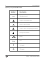
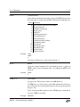
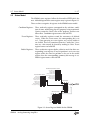
Operation and Service Manual
Analog Summing Amplifier
SIM980
Stanford Research Systems
Revision 1.8 • May 18, 2006
Certification
Stanford Research Systems certifies that this product met its published specifications at the time
of shipment.
Warranty
This Stanford Research Systems product is warranted against defects in materials and workmanship for a period of one (1) year from the date of shipment.
Service
For warranty service or repair, this product must be returned to a Stanford Research Systems
authorized service facility. Contact Stanford Research Systems or an authorized representative
before returning this product for repair.
Information in this document is subject to change without notice.
c Stanford Research Systems, Inc., 2005, 2006. All rights reserved.
Copyright Stanford Research Systems, Inc.
1290–D Reamwood Avenue
Sunnyvale, CA 94089 USA
Phone: (408) 744-9040 • Fax: (408) 744-9049
www.thinkSRS.com • e-mail: [email protected]
Printed in U.S.A.
SIM980
Analog Summing Amplifier
Contents
General Information
Symbols . . . . . . . . . . . . . . . . . . . . . . . . . . . . .
Notation . . . . . . . . . . . . . . . . . . . . . . . . . . . . .
Specifications . . . . . . . . . . . . . . . . . . . . . . . . . .
iii
iv
v
vi
1
Getting Started
1.1 Introduction to the Instrument . . . . . . . . . . . .
1.2 Front-Panel Operation . . . . . . . . . . . . . . . . .
1.3 SIM Interface . . . . . . . . . . . . . . . . . . . . . . .
1–1
. 1–2
. 1–2
. 1–4
2
Remote Operation
2.1 Index of Common Commands .
2.2 Alphabetic List of Commands .
2.3 Introduction . . . . . . . . . . .
2.4 Commands . . . . . . . . . . . .
2.5 Status Model . . . . . . . . . . .
.
.
.
.
.
2–1
. 2–2
. 2–4
. 2–6
. 2–6
. 2 – 17
.
.
.
.
.
.
3–1
. 3–2
. 3–2
. 3–2
. 3–4
. 3–6
. 3–7
Circuitry
4.1 Circuit Descriptions . . . . . . . . . . . . . . . . . . .
4.2 Parts Lists . . . . . . . . . . . . . . . . . . . . . . . .
4.3 Schematic Diagrams . . . . . . . . . . . . . . . . . .
4–1
. 4–2
. 4–4
. 4–5
3
4
.
.
.
.
.
Performance Tests
3.1 Introduction . . . . . . . . . . . .
3.2 Tools and preparation . . . . . .
3.3 Precalibration Values . . . . . . .
3.4 Calibration . . . . . . . . . . . . .
3.5 Other tests and adjustments . . .
3.6 SIM980 Performance Test Record
.
.
.
.
.
.
.
.
.
.
.
.
.
.
.
.
.
.
.
.
.
.
.
.
.
.
.
.
.
.
.
.
.
.
.
.
.
.
.
.
.
.
.
.
.
.
.
.
.
.
.
.
.
.
.
.
.
.
.
.
.
.
.
.
.
.
.
.
.
.
.
.
.
.
.
.
.
.
.
.
.
.
.
.
.
.
.
.
.
.
.
.
.
.
.
.
.
.
.
.
.
.
.
.
.
.
.
.
.
.
i
ii
Contents
SIM980 Analog Summing Amplifier
General Information
The SIM980 Summing Amplifier, part of Stanford Research Sysetems’
Small Instrumentation Modules family, is a four-input, unity-gain
amplifier for combining multiple analog signals from DC to 1 MHz.
Service
Do not install substitute parts or perform any unauthorized modifications to this instrument.
The SIM980 is a single-wide module designed to be used inside the
SIM900 Mainframe. Do not turn on the power until the module is
completely inserted into the mainframe and locked in place.
iii
iv
General Information
Symbols you may Find on SRS Products
Symbol
Description
Alternating current
Caution - risk of electric shock
Frame or chassis terminal
Caution - refer to accompanying documents
Earth (ground) terminal
Battery
Fuse
On (supply)
Off (supply)
SIM980
Analog Summing Amplifier
General Information
v
Notation
The following notation will be used throughout this manual.
WARNING
A warning means that injury or death is possible if the instructions
are not obeyed.
CAUTION
A caution means that damage to the instrument or other equipment
is possible.
Typesetting conventions used in this manual are:
• Front-panel buttons are set as [Button];
[Adjust ] is shorthand for “[Adjust ] & [Adjust ]”.
• Front-panel indicators are set as Overload.
• Remote command names are set as *IDN?.
• Literal text other than command names is set as OFF.
Remote command examples will all be set in monospaced font. In
these examples, data sent by the host computer to the SIM980 are set
as straight teletype font, while responses received by the host
computer from the SIM980 are set as slanted teletype font.
SIM980
Analog Summing Amplifier
vi
General Information
Specifications
Performance Characteristics
Number of inputs
Function
Gain
Input impedance
Bandwidth
Output voltage noise
Crosstalk
Offset voltage
Input range
Output range
Input slew rate
Total Harmonic Distortion
Output slew rate
Operating temperature
Power
4
Inverting, non-inverting, or off
1×
1 MΩ
DC to 1 MHz
√
30 nV/ Hz@ 1 kHz, max.
−80 dB @ 1 kHz
±100 µV (after 5 min. warm up)
±10 V before overload
±10 V before overload
40 V/µs
0.01% (−80 dB) max. @ 1 kHz
75 V/µs
0 ◦ C to 40 ◦ C, non-condensing
+5 V (100 mA)
±15 V (300 mA)
General Characteristics
Interface
Connectors
Weight
Dimensions
Serial (RS-232) through SIM interface
BNC (5 front, 1 rear)
DB–15 (male) SIM interface
1.5 lbs
1.500 W × 3.600 H × 7.000 D
SIM980
Analog Summing Amplifier
1
Getting Started
This chapter gives you the necessary information to get started
quickly with the SIM980 Summing Amplifier.
In This Chapter
1.1
1.2
1.3
Introduction to the Instrument
1.1.1 Overview . . . . . . . .
1.1.2 Power-on State . . . . .
Front-Panel Operation . . . . .
1.2.1 Inputs . . . . . . . . . .
1.2.2 Output . . . . . . . . . .
SIM Interface . . . . . . . . . .
1.3.1 SIM interface connector
1.3.2 Direct interfacing . . . .
.
.
.
.
.
.
.
.
.
.
.
.
.
.
.
.
.
.
.
.
.
.
.
.
.
.
.
.
.
.
.
.
.
.
.
.
.
.
.
.
.
.
.
.
.
.
.
.
.
.
.
.
.
.
.
.
.
.
.
.
.
.
.
.
.
.
.
.
.
.
.
.
.
.
.
.
.
.
.
.
.
.
.
.
.
.
.
.
.
.
.
.
.
.
.
.
.
.
.
.
.
.
.
.
.
.
.
.
1–2
1–2
1–2
1–2
1–3
1–4
1–4
1–4
1–4
1–1
1–2
1.1
Getting Started
Introduction to the Instrument
The SIM980 Summing Amplifier is a four-input, unity-gain amplifier
for combining multiple analog signals from DC to 1 MHz.
1.1.1
Overview
The basic function of the SIM980 is to add or subtract up to four
analog signals. Each input channel can be separately configured for
inverting or non-inverting operation, or switched off. Each input is
1 MΩ and DC-coupled, and accepts signals between ±10 V.
1.1.2
Power-on State
The SIM980 stores its operation state (input channel configuration)
in non-volatile memory. At power-on, the SIM980 will return to its
previous configuration after a brief system check and initialization.
1.2
Front-Panel Operation
The front panel of the SIM980 (see Figure 1.1) provides a simple
operator interface.
Figure 1.1: The SIM980 front and rear panels.
SIM980
Analog Summing Amplifier
1.2
Front-Panel Operation
1.2.1
1–3
Inputs
Each of the four input channels of the SIM980 has a front-panel block
consisting of the BNC input connector, a control button, and several
LED indicators.
1.2.1.1
Polarity toggle
Each input can be switched between inverting or non-inverting polarity by briefly pressing that channel’s control button. When inverting, the − LED is illuminated; when non-inverting, + is lit. Note
that the polarity is always displayed, independent of whether that
channel is on or off.
1.2.1.2
On/Off toggle
Each input can independently be turned on or off by holding that
channel’s control button for ∼1.5 seconds. When on, the channel is
either added to or subtracted from the output (depending on polarity,
section 1.2.1.1). When off, it does not contribute to the output signal
at all. The OFF LED is lit to indicate when a channel is off.
Unused channels should be turned off rather than simply left unconnected, as the Johnson noise of the open 1 MΩ input resistor will
dominate the output noise of the SIM980.
1.2.1.3
Offset autocalibration
The SIM980 uses an active input offset correction to trim all input
circuitry as well as the summing circuitry of DC offsets. The user
can initiate an autocalibration cycle by disconnecting all inputs and
outputs from the SIM980, and pressing and holding any of the control buttons for ∼5 seconds. The entire process takes approximately
1 minute, and is completed when the relays have stopped “clicking”
for at least 10 seconds.
Note that it is important that all inputs be open (or, preferably, shorted
to ground) before initiating an offset autocalibration cycle. If any
input channel is above ∼500 µV amplitude, the SIM980 will reject the
autocalibration request.
1.2.1.4
Input Overload
Each of the four input channels of the SIM980 has an overload detection circuit. The input is considered overloaded when the signal
magnitude exceeds ±10 V. This is indicated by the red OVLD LED at
the top of each front-panel block.
SIM980
Analog Summing Amplifier
1–4
1.2.2
Getting Started
Output
The resulting sum of the enabled input channels appears at the output
BNC connectors on the front and rear panels. Each output connection
is through a 50 Ω resistor. For normal operation, the user should not
need to terminate the output. If a 50 Ω termination is applied, note
that the output signal will be divided in half.
If the output signal exceeds ±10 V, the output overload detection is
activated. This is indicated by the red OVLD near the top of the
“OUTPUT” block on the front panel.
1.3
SIM Interface
The primary connection to the SIM980 Summing Amplifier is the
rear-panel DB–15 SIM interface connector. Typically, the SIM980 is
mated to a SIM900 Mainframe via this connection, either through
one of the internal Mainframe slots, or the remote cable interface.
It is also possible to operate the SIM980 directly, without using the
SIM900 Mainframe. This section provides details on the interface.
CAUTION
1.3.1
The SIM980 has no internal protection against reverse polarity, missing
supply, or overvoltage on the power supply pins. Misapplication of power
may cause circuit damage. SRS recommends using the SIM980 together
with the SIM900 Mainframe for most applications.
SIM interface connector
The DB–15 SIM interface connector carries all the power and communications lines to the instrument. The connector signals are specified
in Table 1.1
1.3.2
Direct interfacing
The SIM980 is intended for operation in the SIM900 Mainframe, but
users may wish to directly interface the module to their own systems
without the use of additional hardware.
The mating connector needed is a standard DB–15 receptacle, such as
Amp part # 747909-2 (or equivalent). Clean, well-regulated supply
voltages of ±15,+5 VDC must be provided, following the pin-out
specified in Table 1.1. Ground must be provided on pins 1 and 8,
with chassis ground on pin 9. The −STATUS signal may be monitored
on pin 2 for a low-going TTL-compatible output indicating a status
message.
SIM980
Analog Summing Amplifier
1.3
SIM Interface
Pin
1
2
3
4
5
6
7
8
9
10
11
12
13
14
15
1–5
Direction
Src ⇒ Dest
Signal
SIGNAL GND
−STATUS
RTS
CTS
−REF 10MHZ
−5 V
−15 V
PS RTN
CHASSIS GND
TXD
RXD
+REF 10MHz
+5 V
+15 V
+24 V
MF ⇒ SIM
SIM ⇒ MF
MF ⇒ SIM
SIM ⇒ MF
MF ⇒ SIM
MF ⇒ SIM
MF ⇒ SIM
MF ⇒ SIM
MF ⇒ SIM
SIM ⇒ MF
MF ⇒ SIM
MF ⇒ SIM
MF ⇒ SIM
MF ⇒ SIM
Description
Ground reference for signal
Status/service request (GND = asserted, +5 V= idle)
HW handshake (+5 V= talk; GND = stop)
HW handshake (+5 V= talk; GND = stop)
10 MHz reference (no connection in SIM980)
Power supply (no connection in SIM980)
Power supply
Power supply return
Chassis ground
Async data (start bit = “0”= +5 V; “1” = GND)
Async data (start bit = “0”= +5 V; “1” = GND)
10 MHz reference (no connection in SIM980)
Power supply
Power supply
Power supply (no connection in SIM980)
Table 1.1: SIM Interface Connector Pin Assignments, DB-15
1.3.2.1
Direct interface cabling
If the user intends to directly wire the SIM980 independent of the
SIM900 Mainframe, communication is usually possible by directly
connecting the appropriate interface lines from the SIM980 DB–15
plug to the RS-232 serial port of a personal computer.1 Connect RXD
from the SIM980 directly to RD on the PC, TXD directly to TD, and
similarly RTS→RTS and CTS→CTS. In other words, a null-modem
style cable is not needed.
To interface directly to the DB–9 male (DTE) RS-232 port typically
found on contemporary personal computers, a cable must be made
with a female DB–15 socket to mate with the SIM980, and a female
DB–9 socket to mate with the PC’s serial port. Separate leads from
the DB–15 need to go to the power supply, making what is sometimes
know as a “hydra” cable. The pin-connections are given in Table 1.2.
1.3.2.2
Serial settings
The initial serial port settings at power-on are: 9600 Baud, 8–bits, no
parity, 1 stop bit, and RTS/CTS flow control. The serial baud rate is
fixed, but the word size and parity may be changed with the FLOW
or PARI commands.
1
SIM980
Although the serial interface lines on the DB-15 do not satisfy the minimum
voltage levels of the RS-232 standard, they are typically compatible with desktop
personal computers
Analog Summing Amplifier
1–6
Getting Started
DB–15/F to SIM980
Name
DB–9/F
3 ←→ 7
4 ←→ 8
10 ←→ 3
11 ←→ 2
5
7 ←→
13 ←→
14 ←→
8,9 ←→
1 ←→
RTS
CTS
TxD
RxD
Computer Ground
to P/S
−15 VDC
+5 VDC
+15 VDC
Ground (P/S return current)
Signal Ground (separate wire to Ground)
Table 1.2: SIM980 Direct Interface Cable Pin Assignments
SIM980 Analog Summing Amplifier
2
Remote Operation
This chapter describes operating the SIM980 over the serial interface.
In This Chapter
2.1
2.2
2.3
2.4
2.5
Index of Common Commands . . . . . . . . . . . .
Alphabetic List of Commands . . . . . . . . . . . .
Introduction . . . . . . . . . . . . . . . . . . . . . . .
2.3.1 Power-on configuration . . . . . . . . . . . .
2.3.2 Buffers . . . . . . . . . . . . . . . . . . . . . .
2.3.3 Device Clear . . . . . . . . . . . . . . . . . . .
Commands . . . . . . . . . . . . . . . . . . . . . . .
2.4.1 Command Syntax . . . . . . . . . . . . . . . .
2.4.2 Notation . . . . . . . . . . . . . . . . . . . . .
2.4.3 Examples . . . . . . . . . . . . . . . . . . . .
2.4.4 Amplifier Commands . . . . . . . . . . . . .
2.4.5 Autocalibration Commands . . . . . . . . . .
2.4.6 Serial Communication Commands . . . . . .
2.4.7 Status Commands . . . . . . . . . . . . . . .
2.4.8 Interface Commands . . . . . . . . . . . . . .
Status Model . . . . . . . . . . . . . . . . . . . . . .
2.5.1 Status Byte (SB) . . . . . . . . . . . . . . . . .
2.5.2 Service Request Enable (SRE) . . . . . . . . .
2.5.3 Standard Event Status (ESR) . . . . . . . . .
2.5.4 Standard Event Status Enable (ESE) . . . . .
2.5.5 Communication Error Status (CESR) . . . . .
2.5.6 Communication Error Status Enable (CESE)
2.5.7 Overload Status (OVCR) . . . . . . . . . . . .
2.5.8 Overload Status (OVSR) . . . . . . . . . . . .
2.5.9 Overload Status Enable (OVSE) . . . . . . . .
2–2
2–4
2–6
2–6
2–6
2–6
2–6
2–7
2–8
2–8
2–9
2 – 10
2 – 11
2 – 11
2 – 13
2 – 17
2 – 18
2 – 19
2 – 19
2 – 19
2 – 20
2 – 20
2 – 21
2 – 21
2 – 21
2–1
2–2
2.1
Remote Operation
Index of Common Commands
symbol
i,j
z
definition
Integers
Literal token
(?)
var
{var}
[var]
Required for queries; illegal for set commands
parameter always required
required parameter for set commands; illegal for queries
optional parameter for both set and query forms
Amplifier
CHAN(?) i {,j}
READ? [i]
2 – 9 Channel Control
2 – 9 Read Offset Voltage
Autocalibration
ARMC(?) [z]
ACAL
OFST(?) i {,j}
2 – 10 Arm Autocalibration
2 – 10 Perform Offset Autocalibration
2 – 10 Offset Value
Serial Communications
FLOW(?) {z}
2 – 11 Flow Control
PARI(?) {z}
2 – 11 Parity
Status
*STB? [i]
*SRE(?) [i,] {j}
*CLS
*ESR? [i]
*ESE(?) [i,] {j}
CESR? [i]
CESE(?) [i,]{j}
OVCR? [i]
OVSR? [i]
OVSE(?) [i,]{j}
PSTA(?) {z}
2 – 11
2 – 11
2 – 12
2 – 12
2 – 12
2 – 12
2 – 12
2 – 12
2 – 13
2 – 13
2 – 13
Status Byte
Service Request Enable
Clear Status
Standard Event Status
Standard Event Status Enable
Comm Error Status
Comm Error Status Enable
Overload Condition
Overload Status
Overload Status Enable
Pulse −STATUS Mode
Interface
*RST
*IDN?
*OPC(?)
CONS(?) {z}
LEXE?
LCME?
2 – 13
2 – 14
2 – 14
2 – 14
2 – 14
2 – 15
Reset
Identify
Operation Complete
Console Mode
Execution Error
Command Error
SIM980
Analog Summing Amplifier
2.1
Index of Common Commands
LBTN?
TOKN(?) {z}
TERM(?) {z}
SIM980
Analog Summing Amplifier
2–3
2 – 15 Button
2 – 15 Token Mode
2 – 16 Response Termination
2–4
2.2
Remote Operation
Alphabetic List of Commands
?
*CLS
*ESE(?) [i,] {j}
*ESR? [i]
*IDN?
*OPC(?)
*RST
*SRE(?) [i,] {j}
*STB? [i]
2 – 12
2 – 12
2 – 12
2 – 14
2 – 14
2 – 13
2 – 11
2 – 11
Clear Status
Standard Event Status Enable
Standard Event Status
Identify
Operation Complete
Reset
Service Request Enable
Status Byte
A
ACAL
ARMC(?) [z]
2 – 10 Perform Offset Autocalibration
2 – 10 Arm Autocalibration
C
CESE(?) [i,]{j}
CESR? [i]
CHAN(?) i {,j}
CONS(?) {z}
2 – 12
2 – 12
2–9
2 – 14
Comm Error Status Enable
Comm Error Status
Channel Control
Console Mode
F
FLOW(?) {z}
2 – 11 Flow Control
L
LBTN?
LCME?
LEXE?
2 – 15 Button
2 – 15 Command Error
2 – 14 Execution Error
O
OFST(?) i {,j}
OVCR? [i]
OVSE(?) [i,]{j}
OVSR? [i]
2 – 10
2 – 12
2 – 13
2 – 13
Offset Value
Overload Condition
Overload Status Enable
Overload Status
P
PARI(?) {z}
PSTA(?) {z}
2 – 11 Parity
2 – 13 Pulse −STATUS Mode
R
READ? [i]
2 – 9 Read Offset Voltage
SIM980
Analog Summing Amplifier
2.2
Alphabetic List of Commands
2–5
T
TERM(?) {z}
TOKN(?) {z}
SIM980
Analog Summing Amplifier
2 – 16 Response Termination
2 – 15 Token Mode
2–6
2.3
Remote Operation
Introduction
Remote operation of the SIM980 is through a simple command language documented in this chapter. Both set and query forms of
most commands are supported, allowing the user complete control
of the summing amplifier from a remote computer, either through
the SIM900 Mainframe or directly via RS-232 (see Section 1.3.2.1).
See Table 1.1 for specification of the DB–15 SIM interface connector.
2.3.1
Power-on configuration
The settings for the remote interface are 9600 baud with no parity
and hardware flow control, and local echo disabled (CONS OFF).
Most of the SIM980 instrument settings are stored in non-volatile
memory, and at power-on the instrument returns to the state it was
last in when power was removed. Exceptions are noted in the command descriptions.
Reset values of parameters are shown in boldface.
2.3.2
Buffers
Incoming data from the host interface is stored in a 64-byte input
buffer. Characters accumulate in the input buffer until a command
terminator (either hCRi or hLFi) is received, at which point the message is parsed and executed. Query responses from the SIM980 are
buffered in a 64-byte output queue.
If the input buffer overflows, then all data in both the input buffer
and the output queue are discarded, and an error is recorded in the
CESR and ESR status registers.
2.3.3
Device Clear
The SIM980 host interface can be asynchronously reset to its poweron configuration by sending an RS-232-style hbreaki signal. From
the SIM900 Mainframe, this is accomplished with the SIM900 SRST
command; if directly interfacing via RS-232, then use a serial break
signal. After receiving the Device Clear, the interface is reset and
CONS mode is turned OFF. Note that this only resets the communication interface; the basic function of the SIM980 is left unchanged;
to reset the instrument, see *RST.
2.4
Commands
This section provides syntax and operational descriptions for reomote commands.
SIM980
Analog Summing Amplifier
2.4
2.4.1
Commands
2–7
Command Syntax
The four letter mnemonic (shown in CAPS) in each command sequence specifies the command. The rest of the sequence consists of
parameters.
Commands may take either set or query form, depending on whether
the “?” character follows the mnemonic. Set only commands are
listed without the “?”, query only commands show the “?” after the
mnemonic, and optionally query commands are marked with a “(?)”.
Parameters shown in { } and [ ] are not always required. Parameters in
{ } are required to set a value, and are omitted for queries. Parameters
in [ ] are optional in both set and query commands. Parameters listed
without any surrounding characters are always required.
Do not send ( ) or { } or [ ] as part of the command.
Multiple parameters are separated by commas. Multiple commands
may be sent on one command line by separating them with semicolons (;) so long as the input buffer does not overflow. Commands
are terminated by either hCRi or hLFi characters. Null commands
and whitespace are ignored. Execution of command(s) does not
begin until the command terminator is received.
tokens Token parameters (generically shown as z in the command de-
scriptions) can be specified either as a keyword or integer value.
Command descriptions list the valid keyword options, with each
keyword followed by its corresponding integer value. For example,
to set the response termination sequence to hCRi+hLFi, the following
two commands are equivalent:
TERM CRLF
—or—
TERM 3
For queries that return token values, the return format (keyword or
integer) is specified with the TOKN command.
SIM980
Analog Summing Amplifier
2–8
2.4.2
Remote Operation
Notation
The following table summarizes the notation used in the command
descriptions:
2.4.3
symbol
i,j
z
definition
Integers
Literal token
(?)
var
{var}
[var]
Required for queries; illegal for set commands
parameter always required
required parameter for set commands; illegal for queries
optional parameter for both set and query forms
Examples
Each command is provided with a simple example illustrating its
usage. In these examples, all data sent by the host computer to
the SIM980 are set as straight teletype font, while responses
received the host computer from the SIM980 are set as slanted
teletype font.
The usage examples vary with respect to set/query, optional parameters, and token formats. These examples are not exhaustive, but are
intended to provide a convenient starting point for user programming.
SIM980
Analog Summing Amplifier
2.4
2.4.4
Commands
2–9
Amplifier Commands
CHAN(?) i {,j}
Channel Control
Set (query) input channel i {to state j=(-1, 0, +1)}.
Setting channel i to j=0 will turn that channel off. Setting j=+1 (or
any positive value less than 32767) turns that channel on, and sets
the polarity to non-inverting. Setting j=-1 (or any negative value
greater than −32768) also turns that channel on, but sets the polarity
to inverting.
All four channels can be set or queried simultaneously by setting i=0.
Example: In the following, all four channels are first commanded off, then
channels 1 and 2 are turned on the opposite polarities. Finally, the
single-channel and four-channel queries are shown.
CHAN 0,0
CHAN 1,+1
CHAN 2,-1
CHAN? 2
-1
CHAN? 0
1,-1,0,0
READ? [i]
Read Offset Voltage
Query the output voltage, in tenths of microvolts.
When the offset autocalibration circuitry is active, an internal highgain amplifier is activated to monitor the SIM980 output. This signal
is digitized by an internal analog-to-digital converter. The READ?
query allows the user to directly record this measurement. When
READ? is queried, the high-gain amplifier is turned on. When the
query has finished averaging, the high-gain amplifier is turned off
again.
The optional parameter i is the averaging time, in milliseconds. The
valid range is 10 <i< 10000, with a default value of 1000 (1 second).
The query result is in integer tenths of microvolts. That is, READ?
returns Vout × 107 /V. The total range is (roughly) −1260 <READ?<
27650, corresponding to output voltages in the range −1.26 mV
through +27.6 mV.
Example: READ?
-151
SIM980
Analog Summing Amplifier
2 – 10
2.4.5
Remote Operation
Autocalibration Commands
The SIM980 has an internal offset trimming circuit (see section 1.2.1.3).
The following set of commands provides detailed control over this
subsystem.
ARMC(?) [z]
Arm Autocalibration
Test and set (or query) the armed flag for autocalibration. If z=(FORCE
1), the armed flag is set without testing.
The offset autocalibration proceedure requires that all inputs to the
SIM980 be at 0 V (that is, either open or shorted to ground). The
ARMC command performs a test of all 4 channels to ensure that each
input is less than ∼ 500 µV amplitude. If all four channels are okay,
the armed flag is set; otherwise it is cleared. The entire test takes
about 15 seconds to complete.
If ARMC FORCE is set, the armed flag will be set without performing
any test of the input channels.
Example: ARMC; ARMC?
1
ACAL
Perform Offset Autocalibration
If the armed flag is set (see ARMC, above), an ACAL command will
initiate an offset autocalibration cycle. The entire process takes between 30 s and 90 s, and should ideally be performed only after the
SIM980 has been allowed to warm up at least 30 minutes.
Example: ACAL; *OPC?
1
OFST(?) i {,j}
Offset Value
Set (query) the low-level offset trim for channel i {to j=(0. . . 255)}.
The result of the ACAL command is stored at 6 low-level offset trims.
The OFST allows direct access to these values. The input-channelspecific offset for channels 1 through 4 are stored in i=1 through 4,
respectively. For these settings, increasing j causes the input offset
adjust to decrease by about 6 µV per count.
i=5 and 6 both adjust the summing node offset voltage. Increasing
j for i=5 causes the output voltage to decrease (by about 4.4 µV per
count), while increasing j for i=6 causes the output voltage to increase
(with roughly the same sensitivity).
All 6 offset values can be simultaneously set to a single value j by
OFST 0,j. Note, however, there is no corresponding multi-channel
SIM980
Analog Summing Amplifier
2.4
Commands
2 – 11
query.
Values stored by OFST or ACAL are stored in non-volatile memory,
and are not affected by power-cycling or *RST.
Example: OFST? 4
106
2.4.6
Serial Communication Commands
FLOW(?) {z}
Flow Control
Set (query) flow control {to z=(NONE 0, RTS 1, XON 2)}.
After power-on, modules default to FLOW RTS flow control.
Example: FLOW 0
PARI(?) {z}
Parity
Set (query) parity {to z = (NONE 0, ODD 1, EVEN 2, MARK 3, SPACE 4)}.
After power-on, modules default to PARI NONE.
Example: PARI EVEN
2.4.7
Status Commands
The Status commands query and configure registers associated with
status reporting of the SIM980.
*STB? [i]
Status Byte
Reads the Status Byte register [bit i].
Execution of the *STB? query (without the optinal bit i) always causes
the −STATUS signal to be deasserted. Note that *STB? i will not clear
−STATUS, even if bit i is the only bit presently causing the −STATUS
signal. See also the PSTA command.
Example: *STB?
16
*SRE(?) [i,] {j}
Service Request Enable
Set (query) the Service Request Enable register [bit i] {to j}.
Example: *SRE 0,1
SIM980
Analog Summing Amplifier
2 – 12
*CLS
Remote Operation
Clear Status
*CLS immediately clears the ESR, CESR, and OVSR.
Example: *CLS
*ESR? [i]
Standard Event Status
Reads the Standard Event Status Register [bit i].
Upon executing *ESR?, the returned bit(s) of the ESR register are
cleared.
Example: *ESR?
64
*ESE(?) [i,] {j}
Standard Event Status Enable
Set (query) the Standard Event Status Enable Register [bit i] {to j}.
Example: *ESE 6,1
ESE?
64
CESR? [i]
Comm Error Status
Query Comm Error Status Register [for bit i].
Upon executing a CESR? query, the returned bit(s) of the CESR
register are cleared.
Example: CESR?
0
CESE(?) [i,]{j}
Comm Error Status Enable
Set (query) Comm Error Status Enable Register [for bit i] {to j}
Example: CESE?
0
OVCR? [i]
Overload Condition
Query Overload Condition Register [for bit i].
Example: OVCR?
3
SIM980
Analog Summing Amplifier
2.4
Commands
OVSR? [i]
2 – 13
Overload Status
Query Overload Status Register [for bit i].
Upon executing a OVSR? query, the returned bit(s) of the OVSR
register are cleared.
Example: OVSR? 0
1
OVSE(?) [i,]{j}
Overload Status Enable
Set (query) Overload Status Enable Register [bit i] {to j}.
Example: OVSE 16
PSTA(?) {z}
Pulse −STATUS Mode
Set (query) the Pulse −STATUS Mode {to z=(OFF 0, ON 1)}.
When PSTA ON is set, any new service request will only pulse the
−STATUS signal low (for a minimum of 1 µs). The default behavior
is to latch −STATUS low until a *STB? query is received.
At power-on, PSTA is set to OFF.
Example: PSTA?
OFF
2.4.8
Interface Commands
Interface commands provide generic control over the interface between the SIM980 and the host computer.
*RST
Reset
Reset the SIM980 to default configuration.
After *RST, all channels are set to positive polarity, and to off. This
is equivalent to the following command sequence:
CHAN 0,1; CHAN 0,0
Example: *RST
SIM980
Analog Summing Amplifier
2 – 14
*IDN?
Remote Operation
Identify
Read the device identification string.
The identification string is formatted as:
Stanford Research Systems,SIM980,s/n******,ver#.#
where ****** is the 6-digit serial number, and #.# is the firmware
revision level.
Example: *IDN?
Stanford Research Systems,SIM980,s/n003075,ver1.21
*OPC(?)
Operation Complete
Operation Complete. Sets the OPC flag in the ESR register.
The query form *OPC? writes a 1 in the output queue when complete,
but does not affect the ESR register.
Example: *OPC
CONS(?) {z}
Console Mode
Set (query) the Console mode {to z=(OFF 0, ON 1)}.
CONS causes each character received at the Input Buffer to be copied
to the Output Queue.
At power-on and Device-Clear, CONS is set to OFF.
Example: CONS?
0
LEXE?
Execution Error
Query the last execution error code. A query of LEXE? always clears
the error code, so a subsequent LEXE? will return 0. Valid codes are:
Value
0
1
2
3
16
Definition
No execution error since last LEXE?
Illegal value
Wrong token
Invalid bit
Autocalibration not armed
Example: *STB? 12; LEXE?; LEXE?
3
0
The error (3, “Invalid bit,”) is because *STB? only allows bit-specific
queries of 0–7. The second read of LEXE? returns 0.
SIM980
Analog Summing Amplifier
2.4
Commands
LCME?
2 – 15
Command Error
Query the last command error code. A query of LCME? always clears
the error code, so a subsequent LCME? will return 0. Valid codes are:
Value
0
1
2
3
4
5
6
7
8
9
10
11
12
13
14
Definition
No execution error since last LCME?
Illegal command
Undefined command
Illegal query
Illegal set
Missing parameter(s)
Extra parameter(s)
Null parameter(s)
Parameter buffer overflow
Bad floating-point
Bad integer
Bad integer token
Bad token value
Bad hex block
Unknown token
Example: *IDN
LCME?
4
The error (4, “Illegal set”) is due to the missing “?”.
LBTN?
Button
Query the channel number of the last button pressed. A query of
LBTN? always clears the button code, so a subsequent LBTN? will
return 0.
Example: LBTN?
1
TOKN(?) {z}
Token Mode
Set (query) the Token Query mode {to z=(OFF 0, ON 1)}.
If TOKN ON is set, then queries to the SIM module that return tokens will return the text keyword; otherwise they return the decimal
integer value.
Thus, the only possible responses to the TOKN? query are ON and 0.
On reset, TOKN is set to OFF.
Example: TOKN OFF
SIM980
Analog Summing Amplifier
2 – 16
TERM(?) {z}
Remote Operation
Response Termination
Set (query) the htermi sequence {to z=(NONE 0, CR 1, LF 2, CRLF 3,
LFCR 4)}. The htermi sequence is appended to all query responses
sent by the module, and is constructed of ASCII character(s) 13 (carriage return) and 10 (line feed). The token mnemonic gives the
sequence of characters.
At power-on, TERM is set to CRLF.
Example: TERM?
3
SIM980
Analog Summing Amplifier
2.5
2.5
Status Model
2 – 17
Status Model
The SIM980 status registers follow the hierarchical IEEE–488.2 format. A block diagram of the status register array is given in Figure 2.1.
There are three categories of registers in the SIM980 status model:
Condition Registers : These read-only registers correspond to the real-time condition of some underlying physical property being monitored.
Queries return the latest value of the property, and have no
other effect. Condition register names end with CR.
Event Registers : These read-only registers record the occurrence of defined
events. When the event occurs, the corresponding bit is set
to 1. Upon querying an event register, any set bits within it
are cleared. These are sometimes known as “sticky bits,” since
once set, a bit can only be cleared by reading its value. Event
register names end with SR.
Enable Registers : These read/write registers define a bitwise mask for their corresponding event register. If any bit position is set in an event
register while the same bit position is also set in the enable
register, then the corresponding summary bit message is set.
Enable register names end with SE.
Communication Error Status
Standard Event Status
DCAS: Device Clear 7
CTSH: CTS Halted 6
7
RTSH: RTS Halted 5
OVR: Input Buffer Overrun 4
5
HWOVRN: Hardware Overrun 3
NOISE: Noise Error 2
3
FRAME: Framing Error 1
PARITY: Parity Error 0
1
6
4
PON: Power On 7
URQ: User Request 6
7
CME: Command Error 5
EXE: Execution Error 4
5
DDE: Device Error 3
QYE: Query Error 2
3
2
7
7 CESB
INP: Input Buffer Error 1
OPC: Operation Complete 0
1
6
X MSS
0
5
5 ESB
ESE
4
4 IDLE
3
3 undef
ESR
6
4
CESR
2
0
CESE
Overload Status
undef X
undef X
X
X
X
X
undef X
OVLD_OUTPUT 4
X
X
4
4
OVLD_CH4 3
OVLD_CH3 2
3
3
2
2
OVLD_CH2 1
OVLD_CH1 0
1
1
0
0
Status Byte
2
2 undef
1
1 undef
0
SB
0 OVSB
SRE
OVCR OVSR OVSE
Figure 2.1: Status Register Model for the SIM980.
SIM980
Analog Summing Amplifier
-STATUS
2 – 18
2.5.1
Remote Operation
Status Byte (SB)
The Status Byte is the top-level summary of the SIM980 status model.
When masked by the Service Request Enable register, a bit set in the
Status Byte causes the −STATUS signal to be asserted on the rearpanel SIM interface connector.
Typically, −STATUS remains asserted (low) until a *STB? query is
received, at which time −STATUS is deasserted (raised)1 . After clearing the −STATUS signal, it will only be re-asserted in response to a
new status-generating condition.
Weight
Bit
1
2
4
8
16
32
64
128
0
1
2
3
4
5
6
7
Flag
OVSB
undef (0)
undef (0)
undef (0)
IDLE
ESB
MSS
CESB
OVSB : Overload Status Summary Bit. Indicates whether one or more
of the enabled flags in the Overload Status Register has become
true.
IDLE : Indicates that the Input Buffer is empty and the command
parser is idle. Can be used to help synchronize SIM980 query
responses.
ESB : Event Status Bit. Indicates whether one or more of the enabled
events in the Standard Event Status Register is true.
MSS : Master Summary Status. Indicates whether one or more of
the enabled status messages in the Status Byte register is true.
Note that while −STATUS is released by the *STB? query, MSS
is only cleared when the underlying enabled bit message(s) are
cleared.
CESB : Communication Error Summary Bit. Indicates whether one or
more of the enabled flags in the Communication Error Status
Register has become true.
Bits in the Status Byte are not cleared by the *STB? query. These
bits are only cleared by reading the underlying event registers, or by
clearing the corresponding enable registers.
1
but see the PSTA command
SIM980
Analog Summing Amplifier
2.5
2.5.2
Status Model
2 – 19
Service Request Enable (SRE)
Each bit in the SRE corresponds one-to-one with a bit in the SB
register, and acts as a bitwise AND of the SB flags to generate the
MSS bit in the SB and the −STATUS signal. Bit 6 of the SRE is
undefined—setting it has no effect, and reading it always returns 0.
This register is set and queried with the *SRE(?) command.
This register is cleared at power-on.
2.5.3
Standard Event Status (ESR)
The Standard Event Status register consists of 8 event flags. These
event flags are all “sticky bits” that are set by the corresponding event,
and cleared only by reading or with the *CLS command. Reading a
single bit (with the *ESR? i query) clears only bit i.
Weight
Bit
1
2
4
8
16
32
64
128
0
1
2
3
4
5
6
7
Flag
OPC
INP
QYE
DDE
EXE
CME
URQ
PON
OPC : Operation Complete. Set by the *OPC command.
INP : Input Buffer Error. Indicates data has been discarded from the
Input Buffer.
QYE : Query Error. Indicates data in the Output Queue has been lost.
DDE : Device Dependent Error. This bit is undefined in the SIM980.
EXE : Execution Error. Indicates an error in a command that was
successfully parsed. Out-of-range parameters are an example.
The error code can be queried with LEXE?.
CME : Command Error. Indicates a parser-detected error. The error
code can be queried with LCME?.
URQ : User Request. Indicates a front-panel button was pressed.
PON : Power On. Indicates that an off-to-on transition has occurred
2.5.4
Standard Event Status Enable (ESE)
The ESE acts as a bitwise AND with the ESR register to produce the
single bit ESB message in the Status Byte Register (SB). It can be set
and queried with the *ESE(?) command.
SIM980
Analog Summing Amplifier
2 – 20
Remote Operation
This register is cleared at power-on.
2.5.5
Communication Error Status (CESR)
The Communication Error Status register consists of 8 event flags;
each of which is set by the corresponding event, and cleared only by
reading or with the *CLS command. Reading a single bit (with the
CESR? i query) clears only bit i.
Weight
Bit
1
2
4
8
16
32
64
128
0
1
2
3
4
5
6
7
Flag
PARITY
FRAME
NOISE
HWOVRN
OVR
RTSH
CTSH
DCAS
PARITY : Parity Error. Set by serial parity mismatch on incoming data
byte.
FRAME : Framing Error. Set when an incoming serial data byte is missing
the STOP bit.
NOISE : Noise Error. Set when an incoming serial data byte does not
present a steady logic level during each asynchronous bitperiod window.
HWOVRN : Hardware Overrun. Set when an incoming serial data byte is
lost due to internal processor latency. Causes the Input Buffer
to be flushed, and resets the command parser.
OVR : Input Buffer Overrun. Set when the Input Buffer is overrun
by incoming data. Causes the Input Buffer to be flushed, and
resets the command parser.
RTSH : Undefined for the SIM980. Command Error. Indicates a parserdetected error.
CTSH : Undefined for the SIM980.
DCAS : Device Clear. Indicates the SIM980 received the Device Clear
signal (an RS-232 hbreaki). Clears the Input Buffer and Output
Queue, and resets the command parser.
2.5.6
Communication Error Status Enable (CESE)
The CESE acts as a bitwise AND with the CESR register to produce
the single bit CESB message in the Status Byte Register (SB). It can
be set and queried with the CESE(?) command.
SIM980
Analog Summing Amplifier
2.5
Status Model
2 – 21
This register is cleared at power-on.
2.5.7
Overload Status (OVCR)
The Overload Condition Register consists of 5 single-bit monitors of
conditions within the SIM980. Bits in the OVCR reflect the real-time
values of their corresponding signals. Reading the entire register, or
individual bits within it, does not affect the OVCR.
Weight
Bit
1
2
4
8
16
32
64
128
0
1
2
3
4
5
6
7
Flag
Overload Channel 1
Overload Channel 2
Overload Channel 3
Overload Channel 4
Overload Output
undef (0)
undef (0)
undef (0)
Overload Channel n : The input buffer for Channel n is overloaded (input voltage
exceeds ±10 V). Note that the overload detection is active even
if the channel is off.
Overload Output : The output of the summing amplifier is overloaded (output
voltage exceeds ±10 V). Note that the output can overload without any input channel overloading, and vice versa.
2.5.8
Overload Status (OVSR)
The Overload Status Register consists of (latching) event flags that
correspond one-to-one with the bits of the OVCR (see above). Upon
the transition 0 → 1 of any bit within the OVCR, the corresponding
bit in the OVSR becomes set.
Bits in the OVSR are unaffected by the 1 → 0 transitions in the OVCR,
and are cleared only by reading or with the *CLS command. Reading
a single bit (with the OVSR? i query) clears only bit i.
2.5.9
Overload Status Enable (OVSE)
The OVSE acts as a bitwise AND with the OVSR register to produce
the single bit OVSB message in the Status Byte Register (SB). It can
be set and queried with the OVSE(?) command.
This register is cleared at power-on.
SIM980
Analog Summing Amplifier
2 – 22
Remote Operation
SIM980 Analog Summing Amplifier
3
Performance Tests
This chapter describes how to adjust the SIM980 to improve its offset
and gain accuracy, and verify performance.
In This Chapter
3.1
3.2
3.3
3.4
3.5
3.6
Introduction . . . . . . . . . . . . .
Tools and preparation . . . . . . .
Precalibration Values . . . . . . .
3.3.1 Offset Voltages . . . . . . .
3.3.2 Calibration Words . . . . .
3.3.3 DC Gain Match . . . . . . .
3.3.4 AC Gain Match . . . . . . .
Calibration . . . . . . . . . . . . .
3.4.1 Offset Adjustment . . . . .
3.4.2 DC Gain Calibration . . . .
3.4.3 AC Gain Calibration . . . .
Other tests and adjustments . . .
SIM980 Performance Test Record
.
.
.
.
.
.
.
.
.
.
.
.
.
.
.
.
.
.
.
.
.
.
.
.
.
.
.
.
.
.
.
.
.
.
.
.
.
.
.
.
.
.
.
.
.
.
.
.
.
.
.
.
.
.
.
.
.
.
.
.
.
.
.
.
.
.
.
.
.
.
.
.
.
.
.
.
.
.
.
.
.
.
.
.
.
.
.
.
.
.
.
.
.
.
.
.
.
.
.
.
.
.
.
.
.
.
.
.
.
.
.
.
.
.
.
.
.
.
.
.
.
.
.
.
.
.
.
.
.
.
3–2
3–2
3–2
3–2
3–3
3–3
3–3
3–4
3–4
3–5
3–5
3–6
3–7
3–1
3–2
3.1
Performance Tests
Introduction
Under typical usage, only the internal autocalibration cycle is
needed to keep the SIM980 operating within specifications (see section 1.2.1.3). If further adjustment is needed, this section describes
the procedure.
3.2
Tools and preparation
The necessary tools for a complete recalibration are:
• a small flat-head screwdriver
• a voltmeter with microvolt resolution and stability (SIM970 or
equivalent)
• a quiet DC voltage source (SIM928 or equivalent)
• a 1 MHz (minimum) sine generator (DS345 or equivalent)
• a 20 MHz bandwidth (minimum) oscilloscope
• several BNC patch cables
• 4 BNC-Tee adapters, or 3 Tees and 1 F/F barrel.
For the full offset calibration procedure the module should be running for at least 15 minute. The trimpots are accessible after removing
the right side panel. It is easier to calibrate the module by connecting
it through a cable to the SIM extension port, but the calibration can
also be performed with the module located in the left-most slot (slot
1) of a SIM900 Mainframe with slots 2–5 empty.
3.3
Precalibration Values
If precalibration values are not required, skip ahead to section 3.4.
Precalibration values should be recorded on a separate copy of the
performance test record (page 3 – 7 ).
3.3.1
Offset Voltages
Begin by disconnecting all inputs from the SIM980, and connecting
the output to the voltmeter. Switch all channels to OFF, and record
the output voltage as “Offset Voltage: Output”. Enable Channel 1,
set the polarity to +, and record the output voltage. Change the
polarity to −, and subtract this output voltage from the previous
value. Record the difference as “Offset Voltage:Channel 1”. Disable
Channel 1, and repeat for the remaining 3 channels.
SIM980
Analog Summing Amplifier
3.3
3.3.2
Precalibration Values
3–3
Calibration Words
Next, query the SIM980 over the remote interface to determine the
calibration word values. Send the remote queries:
OFST? 1
...
OFST? 6
and record the results.
3.3.3
DC Gain Match
Set the DC voltage source to 2 V. Connect the BNC-Tee adapters
together to form a 1-to-4 splitter. Connect the splitter to the DC
voltage source, and connect the four SIM980 inputs to the splitter
with equal-length cables (important for AC testing, later). Enable
all four input channels, and set all input polarities to +. Note the
output voltage as V1+ . Then change all four input polarities to −,
and note the output voltage as V1− .
Now switch the DC voltage source to −2 V, and with the channel
polarities still set to − note the output voltage as V2− . Change all
four input polarities to +, and finally note the output voltage as V2+ .
Calculate the gain ratio mismatch as
!
V1+ − V2+
− 1 × 100 %
V1− − V2−
and record this value as the “DC mismatch”.
3.3.4
AC Gain Match
Using the same 1-to-4 splitter from section 3.3.3, connect all four
input channels to the sine generator, set to create a 1 MHz sine wave
at 1 Vrms or 1 Vpeak-peak amplitude (circle which). Unlike the DC
case, here it is important that all four BNC cables leading to the
channel inputs are of exactly the same length and type and that
the splitting of the signal is accomplished in a symmetric manner.
Differences in cable length will introduce phase shifts between inputs
and falsify the result.
Connect the output of the SIM980 to the oscilloscope. Separately
trigger the scope synchronously with the sine generator.
AC matching is measured pairwise between channels, with the two
channels under test set to opposite polarity and the remaining two
channels switched off. There are 12 such permutations, which can
be labeled with a +− notation. For example, setting Channel 1
SIM980
Analog Summing Amplifier
3–4
Performance Tests
non-inverting, Channel 3 inverting, and Channels 2 & 4 off is noted
as “+−”. Measure the amplitude for each permutation, and
record the results (circle either RMS or peak-to-peak)
3.4
Calibration
Prior to beginning calibration, photocopy a blank version of the performance test record (page 3 – 7 ).
3.4.1
Offset Adjustment
Calibration starts by disconnecting all inputs and resetting the electronic output offset calibration constants. This is accomplished by
issuing the remote commands:
CHAN 0,0
OFST 5, 128; OFST 6, 127
which set the electronic trim-DAC outputs to midpoint. Connect the
SIM980 output to the voltmeter, and adjust R245 to zero the voltage
reading.
After nulling R245, an unconditional autocalibration cycle should be
initiated. Issue the following remote commands:
ARMC FORCE; ACAL
to arm and start internal calibration. The autocalibration will complete in approximately one minute (wait for relays to cease switching
for at least 10 seconds). The output voltage will fluctuate during calibration but settle to less than ±20 µV.
Verify that the calibration words are within the valid range 1–254
by repeating the queries of section 3.3.2. Nominally, all calibration
words should be within the range 50–200; values of 0 or 255 indicate
that the offsets have shifted outside of the adjustable range and the
SIM980 may be damaged.
Input offset voltages should be measured directly by the procedure
of section 3.3.1. Except for short term drift, the calibration should
reduce input offset voltage errors to less than 10 µV. If the result is unsatisfactory, adjustment of the calibration constant may be attempted
by manually issuing explicit OFST commands (see section 2.4.5).
Manually adjusted constants should differ only slightly (±1 count)
from the automatic result. Otherwise the module should be powercycled and the adjustment procedure should be repeated.
Record the final offset values, and final calibration words, on the
performance test record.
SIM980
Analog Summing Amplifier
3.4
3.4.2
Calibration
3–5
DC Gain Calibration
All resistors of the SIM980 gain network have a precision of 0.1%.
Any two channels can therefore differ in their gain by up to 0.2%.
Gain between + and − polarity settings can also differ by 0.2%. The
common mode rejection of two channels set to take the difference
of two signals is therefore limited to 0.2% or approximately −54 dB
worst case. The module has one trimpot to equalize the average
positive gain (over all channels) with the average negative gain and
give the best overall match for any combination of channels.
To find the optimum setting, repeat the setup of section 3.3.3. Set
the DC voltage source to approximately 2 V output, and set all four
input channels to − polarity. Note the DC output voltage with at
least millivolt precision (the value should be ∼ −8.00 V. Now switch
all four channels to +, and adjust trimpot R268 to bring the output
voltage to the same magnitude, but opposite polarity, as previously
noted. Be aware that this procedure depends on neglecting the input
offset voltages, so be sure to perform section 3.4.1 first.
After completing the calibration, measure the DC gain match according to section 3.3.3, and record the results.
3.4.3
AC Gain Calibration
The SIM980 amplifier bandwidth rolls off around 6 MHz. This is accomplished with a combination of fixed capacitors and one trimcap.
The trimcap can be adjusted to equalize high-frequency gain below
approximately 1 MHz, maximizing the average common mode rejection between channels.
Just as in case of the DC gain, the module achieves matching on the
order of −60 dB. Above 1 MHz, high order effects begin to dominate
and AC gains will vary from channel to channel by more than −50 dB.
However, even the worst case channels typically achieve −40 dB (1%
gain difference) suppression for any frequency below their −3 dB
bandwidth as long as all amplifiers operate in small signal mode
(i.e., the slew rate limit is not exceeded). For sinusoidal signals, this
translates into 10 V amplitude at 500 kHz and 1 V at 5 MHz. Care
must be taken with non-sinusoidal signals which have high slew
rate.
For this adjustment a 1 MHz sine wave generator and an AC voltmeter or oscilloscope are necessary. Connect the instruments as
previously in section 3.3.4.
Again, it is crucial that all BNC cables are of exactly the same length
and type and that the splitting of the signal is accomplished in a
symmetric manner. Differences in cable length will introduce phase
SIM980
Analog Summing Amplifier
3–6
Performance Tests
shifts between inputs and falsify the result. If in doubt, as a check of
symmetric cabling, the measurments may be repeated with the inputs
being connected to all possible permutations of the four cables.
Inputs are pairwise set to − and + such that the overall AC signal is
nulled. There are twelve possible gain combinations for two channel
nulling:
+− and −+,
+− and −+,
+− and −+,
+− and −+,
+− and −+,
+− and −+.
The combination with the worst common mode rejection is optimized
with trimcap C217 and all other combinations are re-checked. After
a few iterations a solution with well distributed error can be found.
The residual worst case AC voltage will typically be approximately
5 mVrms for a 1 Vrms input.
After completing the adjustments, record the results.
Some users might want to improve DC and AC matching for a single
combination of channels (e.g. channels 1 & 2) while sacrificing the
matching for the others. This can be accomplished best by driving
the two channels with the same signal and operating one in positive
and the other one in negative mode while using R268 and C217 to
minimize the difference signal at the output. Please note that reversing the polarity of these two channels will not result in an equally
well matched result. The procedure works within a narrower-thanspecified temperature range, and long term drift might make frequent re-calibration necessary.
3.5
Other tests and adjustments
The SIM980 internally generates two precision power supply voltages for the input buffer amplifiers. These +13.0 V and −13.0 V voltages can be tested at test points TP401 (+13.0 V), TP402 (−13.0 V) and
TP403 (ground). R405 and R402 can be used to adjust the −13.0 V and
+13.0 V voltage. There should be no need to ever actually perform
this factory adjustment. If either voltage shows a large (> 100 mV)
deviation from its ideal value, the module might have been damaged
and should be sent to the factory for repair.
SIM980
Analog Summing Amplifier
3.6
3.6
SIM980 Performance Test Record
3–7
SIM980 Performance Test Record
This page should be photocopied to record results.
General
Offset Voltage
Calibration Words
Gain
Name:
Serial Number:
µV
µV
µV
µV
µV
Output:
Channel 1:
Channel 2:
Channel 3:
Channel 4:
OFST?
OFST?
OFST?
OFST?
OFST?
OFST?
1
2
3
4
5
6
DC mismatch:
AC mismatch:
(@ 1 MHz, 1 V
rms / peak-peak)
SIM980
Date/Time:
Analog Summing Amplifier
%
+−:
−+:
+−:
−+:
+−:
−+:
+−:
−+:
+−:
−+:
+−:
−+:
mV (rms / peak-peak)
mV
mV
mV
mV
mV
mV
mV
mV
mV
mV
mV
3–8
Performance Tests
SIM980 Analog Summing Amplifier
4
Parts Lists and Schematics
This chapter presents a brief description of the SIM980 circuit design.
A complete parts list and circuit schematics are included.
In This Chapter
4.1
4.2
4.3
Circuit Descriptions . . . . . . . . . .
4.1.1 Input circuitry . . . . . . . . . .
4.1.2 Summing circuitry . . . . . . .
4.1.3 Output circuitry . . . . . . . . .
4.1.4 Offset measurement & control
4.1.5 Digital control . . . . . . . . . .
Parts Lists . . . . . . . . . . . . . . . .
Schematic Diagrams . . . . . . . . . .
.
.
.
.
.
.
.
.
.
.
.
.
.
.
.
.
.
.
.
.
.
.
.
.
.
.
.
.
.
.
.
.
.
.
.
.
.
.
.
.
.
.
.
.
.
.
.
.
.
.
.
.
.
.
.
.
.
.
.
.
.
.
.
.
4–2
4–2
4–2
4–2
4–3
4–3
4–4
4–5
4–1
4–2
4.1
4.1.1
Circuitry
Circuit Descriptions
Input circuitry
Each channel of the SIM980 Summing Amplifier contains a JFET
unity gain input buffer amplifer (U201–U204) with input protection
(D201–D204). These input buffers have 0.1 µV/◦ C offset voltage drift
and are being automatically trimmed to zero offset voltage by means
of an eight channel digital analog converter U403. Input buffer amplifiers are powered by LDO voltage regulators U401 and U402 which
are set to +13.0 V and −13.0 V, respectively.
Discriminators U205–U208 provide under/overvoltage detection for
each channel and U209 monitors the output voltage. The OVLDALL
signal is generated by or-ing overload signals into a single channel. This signal restarts the module’s microcontroller clock which
is inactive in normal operation to minimize noise. The clock is also
automatically activated by a button push or a serial command.
4.1.2
Summing circuitry
The buffered input signals are summed into precision (0.1%) resistor
networks R200A–E and R201A–E which form a difference amplifier
with gain 1 around the fast precision amplifier U210. The signal path
is controlled by relays K201–K208. A combination of two dual-pole,
dual-throw relays per channel allows enable/disable and polarity
change with constant noise gain and signal bandwidth.
The difference amplifier U210 is buffered by the power buffer U211.
This compound amplifier can drive 10 V signals into open and 5 V
into two 50 Ω loads. The outputs on the front and back panel
can be used simultaneously with resistive isolation between them.
The independent 50 Ω series resistors at these outputs also guarantee unlimited stability for any possible passive load and overcurrent/thermal protection for shorted outputs. The combination of
U210/U211 is rolled off at a bandwith of 4 MHz by the combintion
of C220 and C202. Trim capacitor C217 is factory adjusted for best
common mode suppression at high frequencies.
4.1.3
Output circuitry
Outputs as well as inputs are equipped with common mode filters
(baluns) to reduce conducted EMI (electromagnetic interference) of
RF noise currents on the shield of BNC cables attached to the module.
For the same reason the BNCs are isolated from the SIM980’s front
and back panels. This design ensures the best DC and low frequency
performance in noisy environments. Care must be taken not to load
the ground connections with currents > 1 A which could destroy the
SIM980
Analog Summing Amplifier
4.1
Circuit Descriptions
4–3
differential pair wiring inside the module and disconnect the ground
from the isolated BNC jacks. Such a fault could result in harmful
voltages being present on the BNC shell.
The opamp/buffer combination U210/U211 does not by itself satisfy
the offset voltage specifications of the SIM980. Offset voltage stability is therefore guaranteed by U212, a differential integrator which
drives a differential current source, QN201A/B, to trim the input
offset voltage of U210. The resulting amplifier combines the AC performance of U210 with the stability of the slow amplifier U212. Offset
adjustment is performed by two outputs of digital-analog converter
U403.
4.1.4
Offset measurement & control
Chopper stabilized amplifier U404 is set at a gain of 1000 to measure output offset voltages with the 10-bit, built in analog-digitalconverter of microcontroller U101. In auto-calibration mode the microcontroller can resolve microvolt output voltages and set channels
1–6 of digital-analog-converter U403 to minimize any input and the
output offset voltage. Chopper amplifier U404 is switched off during normal operation to eliminate the potential noise generated by
its internal chopping circuit.
4.1.5
Digital control
The SIM980 is controlled by microcontroller U101.
A critical aspect of the design is the clock-stop circuitry implemented
by U103 and U105. A simple RC-oscillator is enabled or disabled at
pin 1 of U105, which is driven by synchronizing flip-flop U103B to
ensure that no “runt” clock pulses are produced that would violate
U101’s minimum clock periods. Four separate clock-starting signals
are combined by U106:
• Power-on reset
• Amplifier overload (any)
• Incoming serial data
• Front-panel button press
The fast start-time of the RC-oscillator ensures that incoming serial data will be correctly decoded by the microcontroller’s UART,
even when the clock is started by the serial start bit of the incoming
data. When the microcontroller has completed all pending activity,
it drives the STOP signal high (pin 71 of U101), effectively halting its
own processor clock. In this way, the SIM980 guarantees no digital
clock artifacts can be generated during quiescent operation.
SIM980
Analog Summing Amplifier
4–4
4.2
Circuitry
Parts Lists
Part Reference
C101,C102,C103
C104
C105
C106,C107,C108,C405
C201,C203
C202
C204-C215
C217
C218
C220
C222-C223
C401-C404,X101-106,
X108-X114,X201-X224
D101,D102,D402
D103,D104,D205-D207
D201-D204
D301-D308
D309-D313
D314-D317
D401
J101
J103
J201-J206
JS201
JS301
K201-K208
L101,L102,L103
L201-L206
Q101-Q116
Q201-Q206
QN201
R101,R118-119,R122,
R123,R213-216,R240,
R242-243,R260
R102,R201,R203,R205,
R207,R221,R224,R227,
R230,R291,R423
R103
R104,R217-R220,R241,
R261
R105,R295,R296,R298,
R299,R2101
R106,R262,R263
R107-R110,R115
R112,R113, R421,R422
R114,R120,R121,
R409-R414,R424
SRS P/N
5-00098
5-00381
5-00106
5-00387
5-00319
5-00368
5-00318
5-00104
5-00363
5-00313
5-00454
5-00299
Value
10µ T
330p
9.0--50p
1000p
10U/T35
27P
2.2U/T35
3.5-20P
10P
1P
.01U
.1U
3-00945
3-00649
3-00896
3-00424
3-00425
3-00426
3-01384
1-00367
1-00302
1-00003
1-01079
1-01080
3-01492
6-00174
6-00640
3-01421
3-00580
3-01419
4-01527
BAT54S
BAW56LT1
BAV99
GREEN
RED
YELLOW
MMBZ5232BLT1
15 Pin D
Socket 0.100" 3x2
BNC
20 pin
20 Pin
ASX2204H
FR43 Bead
ToroidChoke
MMBT2222A
MMBT3906LT1
MBT3906DW1
100k
4-01479
1.0k
4-01052
4-01495
210
4.7k
4-01511
22k
4-01431
4-01519
4-01551
4-01503
10
47K
1.0M
10K
Part Reference
R116,R124,R125
R117,R126,R127,R223,
R226,R229,R232,R238,
R284-R287,R292
R128,R246,R265,R288
R202,R204,R206,R208
R209,R211
R210,R212
R222,R225,R228,R231,
R267
R233,R239
R234-R237
R245
R249,R252,R255-R259
R250,R251,R253,R254
R266
R268
R289,R290
R401
R402,R405
R403
R404
R406
R407
R408
R415-R420
R425-R428
R431
RN200,RN201
RN301,RN302
S301-S304
U101
U102
U103
U104
U105
U106
U107-U108
U201-U204
U205-U209
U210
U211
U212
U401
U402
U403
U404
U405
SIM980
SRS P/N Value
4-01465 270
4-01455 100
4-01406
4-01405
4-01259
4-01309
4-01535
0
1.00M
30.1K
100K
220K
4-01419
4-01675
4-00617
4-01487
4-01486
4-01541
4-00901
4-01561
4-01402
4-00014
4-01308
4-01310
4-01348
4-01526
4-01517
4-01524
4-01499
4-00925
4-01649
4-00442
2-00053
3-01379
3-00903
3-00742
3-00662
3-01405
3-00663
3-00746
3-01246
3-00728
3-01278
3-01247
3-00998
3-01415
3-01248
3-01279
3-01280
3-01367
3.3
100, 5%, 1/2W
100K
2.2K
2.0K
390k
500K
2.7M
931K
5K
97.6K
102K
255K
91K
39K
75K
6.8K
10
1.000K
1.2K 1206 mini
B3F-1052
68HC912B32
MAX6348 4.4V
74HC74
74HC14
74AC00
74HC08
74HC245
AD8610AR
LM393
AD829AR
BUF634F
OPA277UA
LP2951CMM
LT1175CN8
MAX5258
LTC2050CS5
DG419DY
Analog Summing Amplifier
4.3
4.3
Schematic Diagrams
4–5
Schematic Diagrams
Schematic diagrams follow this page.
SIM980
Analog Summing Amplifier