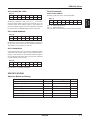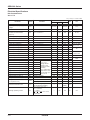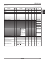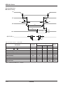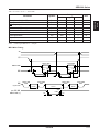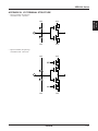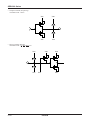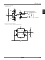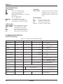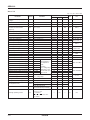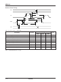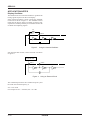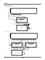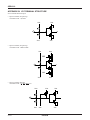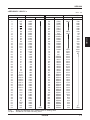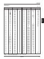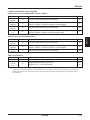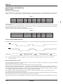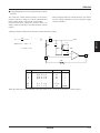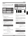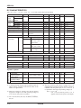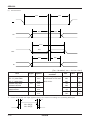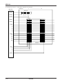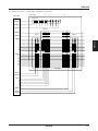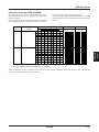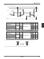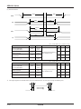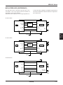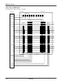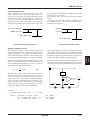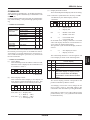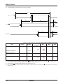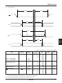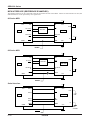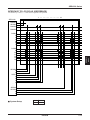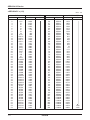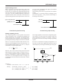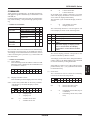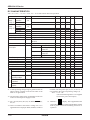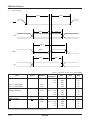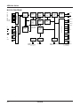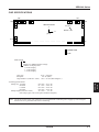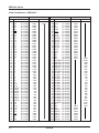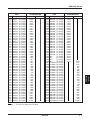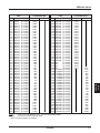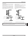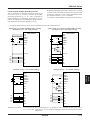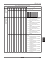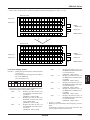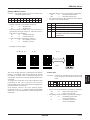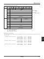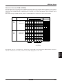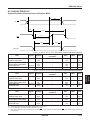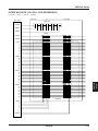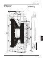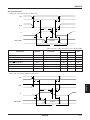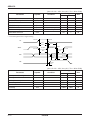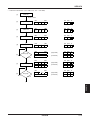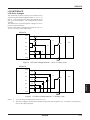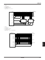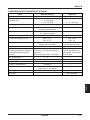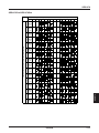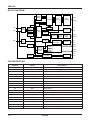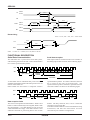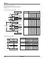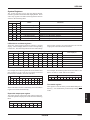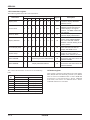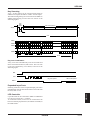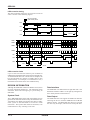
1
MF423-07 s e ri 0 0 2 1 S D E D C L e rs e S iv Co / r e l l o r t n l Dr ic M al Te n ch a a nu NOTICE No parts of this material may be reproduced or duplicated in any form or by any means without the written permission of Seiko Epson. Seiko Epson reserves the right to make changes to this material without notice. Seiko Epson does not assume any liability of any kind aristing out of any inaccuracies contained in this material or due to its application or use in any product or circuit and, further, there is no representation that this material is applicable to products requiring high level reliability, such as, medical products. Moreover, no license to any intellectual property rights is granted by implication or otherwise, and there is no representation or warranty that anything made in accordance with this material will be free from any patent or copyright infringement of a third party. This material or portions thereof may contain technology or the subject relating to strategic products under the control of the Foreign Exchange and Foreign Trade Control Law of Japan and may require an export licence from teh Ministry of International Trade and Industry or other approval from another government agency. Note the following precautions when using semiconductor devices. [Precautions for light] Due to the solar battery principle, the characteristics of the semiconductor devices generally change when the devices are irradiated. This IC, therefore, may malfunction when exposed to light. Since this IC is not completely lightproof, follow the precautions below when using a substrate or product on which it is mounted. (1) Design and mount the substrate or product so as to block out any light from reaching the IC during actual use. (2) For the inspection process, design the environments so as to block out any light from reaching the IC. (3) When blocking out light, take all surfaces of the IC chip into account. © Seiko Epson corporation 1998 All right reserved. i8088 and i8086 are registered trademarks of Intel Corporation. Z80 is registered trademark of Zilog Corporation. V20 and V30 are registered trademarks of Nippon Electric Corporation. CONTENTS 1. Selection Guide 2. SED1200 3. SED1210 4. SED1220 5. SED1225 Series 6. SED1230 Series 7. SED1234/35 Series 8. SED1240 Series 9. SED1278 10. SED1280 SED1200 Series LCD Controller/Drivers Selection Guide ■ LCD controller-drivers for Built-in character generators together with segment and common drivers simplify the small-sized displays Part number Supply voltage LCD voltage range (V) range (V) task of displaying microprocessor messages on small LCDs. Duty Segment Common Display MicroproRAM cessor (characters) interface Extension display output Package SED1200D0A Comment JIS character AI pad chip ASCII character SED1200D0B 4-bit SED1200F0A 50 20 SED1200F0B parallel – JIS character QFP1-80pin ASCII character SED1200F1B 2.5–5.5 3.5–5.5 1/8,1/16 16 QFP14-80pin SED1210D0A JIS character AI pad chip 4 or 8-bit SED1210D0B 40 40 SED1210F0A ASCII character Serial parallel JIS character QFP5-80pin ASCII character SED1210F0B SED1220DXB Au bump chip 26 TCP SED1220TXX 4 or 8-bit SED1221DXB Au bump chip parallel SED1221TXX 2.4–3.6 4.0–7.0 1/18,1/26 62 36 – TCP or 18 SED1220DXA AI pad chip Serial SED122ADXB Au bump chip SED122ATXX TCP SED1225DXB SED1225TXB 4 or 8-bit parallel or Serial SED1278D 4 or 8-bit 1.7–3.6 3.0–6.0 1/18,1/26 64 26 36 – Au bump chip TCP AI pad chip 1/18,1/11, SED1278F LCD static drive allowed Three standard characters (JIS, ASCII, Cellular) 4.5–5.5 3.0–5.5 40 16 80 parallel Serial QFP5-80pin 1/16 SED1280F Serial QFP5-100pin SED1230D Six standard characters (0A/0B/0C/0E/0G/0H) Three standard character (0A/0B/0C) Au bump chip 1/30 30 SED1230T TCP SED1231D Au bump chip 1/23 65 23 SED1231T TCP SED1232D Au bump chip 2.4–3.6 4.0–12.0 48 SED1232T TCP 1/16 16 SED1233D 4 or 8-bit Au bump chip 80 SED1233T parallel TCP – SED1234D 1/30 30 or 16 Serial Built-in power circuit for LCD Three standard characters (JIS, ASCII, Cellular) AI pad chip SED1230/31/32/33 LCD static drive allowed AI pad chip SED1234/35 LCD dynamic drive only. 62 SED1235D 1/16 SED1240DXB Au bump chip 1/34 34 SED1240TXX TCP SED1241DXB Au bump chip 1.8–5.5 5.0–16.0 1/26 80 26 80 SED1241TXX TCP SED1242DXB Au bump chip 1/18 SED1242TXX 18 TCP 1–1 SED1200 Series LCD Controller/Drivers Technical Manual Contents OVERVIEW ......................................................................................................................................................... 2–1 BLOCK DIAGRAM ............................................................................................................................................... 2–2 PINOUT ............................................................................................................................................................... 2–3 PIN DESCRIPTION ............................................................................................................................................. 2–5 COMMAND DESCRIPTION ................................................................................................................................ 2–5 SPECIFICATIONS ............................................................................................................................................... 2–7 OPERATION ...................................................................................................................................................... 2–13 APPLICATION NOTES ...................................................................................................................................... 2–17 APPENDIX A: CHARACTER CODES AND FONTS ........................................................................................ 2–25 APPENDIX B: I/O TERMINAL STRUCTURE ................................................................................................... 2–27 –i– SED1200 Series FEATURES .......................................................................................................................................................... 2–1 OVERVIEW FEATURES The SED1200 is a Liquid Crystal Display (LCD) character display controller-driver, capable of directly driving displays as large as 2 lines of 10 5×8 pixel characters, with a minimum of external components. The SED1200 has an internal character generator (CG) consisting of 160 JIS ASCII characters in ROM and four user definable characters in RAM. The internal CG, a versatile set of cursor and display control commands, mean that the system CPU is only responsible for the display data and commands, and not for the LCD display itself. • Internal display RAM to hold 20 8-bit character codes. • Internal character generator – CGROM: 160 JIS ASCII characters. – CGRAM: 4 user programmable 5×8 pixel characters – Font: 5×7 pixel characters plus the underline cursor. – JIS character set using SED1200F0A/SED1200D0A – ASCII character set using SED1200F 0B / SED1200D0B • Internal LCD driver circuitry – 50 segment driver lines – 16 common driver lines – Total size: Two lines of 10 characters each (maximum). One line of 20 characters (LCD panel dependent) • CPU interface – 4-bit CPU data bus – 13 display control commands • Low external component count – Built in RC oscillator (using one external feedback resistor) – Built in LCD driver voltage-divider network. • Implemented using low power CMOS technology – TTL compatible CPU interface • Power supply – Logic: 2.5 V to 5.5 V – LCD: 3.5 V to 5.5 V • 80 pin QFP package SED1200F and chip (SED1200D) EPSON 2–1 SED1200 Series SED1200 Series SED1200 Series BLOCK DIAGRAM XG Address counter (2) DB0 DB1 DB2 Address decoder DB3 DDRAM COM 1 Common driver CS Address control Address counter (1) Instruction register A0 Input control RD Latch WR Timing generation (2) Oscillator Common signal generator Timing generation (1) ø XD COM 16 Read/Write control Address decoder CGROM Voltage driver Address decoder Voltage level shifter CGRAM control CGRAM Read/Write control Data control Segment signal generator Segment driver SEG 1 2–2 to to EPSON SEG 50 VDD VSS VLCD SED1200 Series PINOUT 60 55 50 45 41 65 40 70 35 SED1200 Series 64 (TOP VIEW) 75 30 80 25 1 5 10 15 20 24 SED1200F Package Outline 20 15 10 5 1 25 80 30 75 35 70 40 65 45 50 55 60 SED1200D Die Outline EPSON 2–3 SED1200 Series TABLE 1. SED1200 Pinout No. 1 2 3 4 5 6 7 8 9 10 11 12 13 14 15 16 17 18 19 20 2–4 NAME SEG17 SEG16 SEG15 SEG14 SEG13 SEG12 SEG11 SEG10 SEG9 SEG8 SEG7 SEG6 SEG5 SEG4 SEG3 SEG2 SEG1 COM1 COM2 COM3 No. 21 22 23 24 25 26 27 28 29 30 31 32 33 34 35 36 37 38 39 40 NAME COM4 COM5 COM6 COM7 COM8 A0 CS RD WR Φ XD XG DB3 DB2 DB1 DB0 VSS VLCD VDD COM9 No. 41 42 43 44 45 46 47 48 49 50 51 52 53 54 55 56 57 58 59 60 EPSON NAME No. COM10 61 COM11 62 COM12 63 COM13 64 COM14 65 COM15 66 COM16 67 SEG50 68 SEG49 69 SEG48 70 SEG47 71 SEG46 72 SEG45 73 SEG44 74 SEG43 75 SEG42 76 SEG41 77 SEG40 78 SEG39 79 SEG38 80 NAME SEG37 SEG36 SEG35 SEG34 SEG33 SEG32 SEG31 SEG30 SEG29 SEG28 SEG27 SEG26 SEG25 SEG24 SEG23 SEG22 SEG21 SEG20 SEG19 SEG18 SED1200 Series CPU Interface Oscillator CS RD WR A0 OSC1, OSC2 Active low chip select input. Active low read enable input. Active low write strobe. Selects between instruction and display data access. A0 = H: Display data A0 = L: Instruction D0–D2 Active high CPU data inputs. D3 Active high CPU data input/output. Φ Clock input for command execution. Terminals for the oscillator external feedback resistor, Rf. If an externally generated clock is used, it is connected to OSC1; OSC2 is left open. Power Supply VDD VLCD VSS Logic power supply LCD power supply System ground (0 V). LCD Interface COM1–COM16 LCD common driver outputs. SEG1–SEG50 LCD segment driver outputs. COMMAND DESCRIPTION Command Summary TABLE 2. SED1200 Command Summary COMMAND NAME CS WR RD A0 D7 D6 D5 D4 D3 D2 D1 D0 REMARKS SET CURSOR DIRECTION 0 0 1 0 0 0 0 0 0 1 0 D/I CURSOR ADDRESS –1/+1 0 0 1 0 0 0 0 0 0 1 1 –1/+1 CURSOR FONT SELECT 0 0 1 0 0 0 0 0 1 0 0 A/U CURSOR BLINK ON/OFF 0 0 1 0 0 0 0 0 1 0 1 ON/OFF D0 = 1 ... ON D0 = 0 ... OFF DISPLAY ON/OFF 0 0 1 0 0 0 0 0 1 1 0 ON/OFF D0 = 1 ... ON D0 = 0 ... OFF CURSOR ON/OFF 0 0 1 0 0 0 0 0 1 1 1 ON/OFF D0 = 1 ... ON D0 = 0 ... OFF SYSTEM RESET 0 0 1 0 0 0 0 1 0 0 0 0 LINE SELECT 0 0 1 0 0 0 0 1 0 0 1 2/1 SET CGRAM ADDRESS 0 0 1 0 0 0 1 0 SET CGRAM DATA 0 0 1 0 0 1 0 SET CURSOR ADDRESS 0 0 1 0 1 SET CHARACTER CODE 0 0 1 1 BUSY FLAG CHECK 0 1 0 0 (LOWER ADDRESS) D0 = 1 ... Decrement D0 = 0 ... Increment D0 = 1 ... Cursor address –1 D0 = 0 ... Cursor address +1 D0 = 1 ... All dots blinking D0 = 0 ... Underline Data RAM & CGRAM are not affected D0 =1 ... 2 line display (1/16 duty) D0 = 0 ... 1 line display (1/8 duty) Upper address fixed at 0H (CGRAM DATA) D6 = 1 ... 2nd line N digit address D6 = 0 ... 1st line N digit address 2nd/1st (N DIGIT-1) (CHARACTER CODE) BF * * * BF EPSON * * * High impedance 2–5 SED1200 Series PIN DESCRIPTION SED1200 Series Write Commands SET CURSOR DIRECTION A0 = 0 D7 D6 0 0 D5 D4 D3 D2 D1 D0 0 0 0 1 0 D CURSOR ON/OFF A0 = 0 D7 D6 D5 D4 0 0 0 D3 D2 D1 D0 1 1 1 D 0 Sets the way in which the cursor address register changes as character data is written to the SED1200 by the CPU, and hence the direction of cursor movement. Controls the display of the cursor. D = 0: Cursor off. D = 1: Cursor on. D = 0: Address register increment direction D = 1: Address register decrement direction SYSTEM RESET A0 = 0 D7 D6 D5 CURSOR ADDRESS –1/+1 A0 = 0 D7 D6 D5 D4 D3 0 0 0 0 0 0 D2 D1 D0 1 1 D Adds one to, or subtracts one from, the current contents of the cursor address register, and hence moves the cursor. D = 0: ADDRESS = ADDRESS + 1 D = 1: ADDRESS = ADDRESS – 1 0 0 D4 D3 D2 D1 D0 1 0 0 0 0 Initializes the SED1200 to the following defaults. 1. CURSOR DIRECTION: Increment 2. CURSOR FONT: Underline 3. CURSOR BLINK: Off 4. DISPLAY: Off 5. CURSOR: Off 6. LINE SELECT: One line display 7. CURSOR ADDRESS: Address 0 (Line 1, character 0) Note: SYSTEM RESET does not affect the contents of the display data RAM, or the CGRAM. CURSOR FONT SELECT A0 = 0 D7 D6 0 0 LINE SELECT D5 D4 D3 D2 D1 D0 0 0 1 0 0 D A0 = 0 D7 D6 0 D = 0: Underline cursor D = 1: All dots blinking CURSOR BLINK ON/OFF A0 = 0 D7 D6 D5 D4 D3 0 0 0 0 1 D2 D1 D0 0 1 D 0 D5 D4 D3 D2 D1 D0 0 1 0 0 1 D Selects the number of displayed lines, and hence the LCD drive duty cycle. D = 0: 1 line display (1/8 duty cycle) D = 1: 2 line display (1/16 duty cycle) Note: The number of lines which can be displayed depends on the LCD panel used. SET CURSOR ADDRESS Controls flashing of the underline cursor. D = 0: Flashing stopped D = 1: Cursor flashing A0 = 0 D7 D6 1 L D5 D4 D3 D2 D1 D0 P5 P4 P3 P2 P1 P0 DISPLAY ON/OFF A0 = 0 D7 D6 0 0 D5 D4 D3 D2 D1 D0 0 0 1 1 0 D Presets the contents of the cursor address register, and hence the position of the cursor. L = 0: Line 1 select L = 1: Line 2 select P5–P0: Position of character in selected line. D = 0: Display Blanked D = 1: Display on Note: This command does not affect the contents of the display data RAM. 2–6 EPSON SED1200 Series Read Commands SET CHARACTER CODE C7 C6 BUSY FLAG CHECK D5 D4 D3 D2 D1 D0 C5 C4 C3 C2 C1 C0 Reading yields the status of the SED1200F. Writes the character code given by C7–C 0 into the character data RAM at the location pointed to by the contents of the cursor address register. The contents of the cursor address register are then modified as specified by the last SET CURSOR DIRECTION instruction. A0 = 0 D7 D6 BF * D5 D4 D3 D2 D1 D0 * * BF * * * BF = 0: SED1200 READY BF = 1: SED1200 BUSY Bits D2–D0 are tristate during reads of the Busy Flag. SET CGRAM ADDRESS A0 = 0 D7 D6 0 0 D5 D4 D3 D2 D1 D0 1 0 * * A1 A0 Presets the contents of the CGRAM address register to the position of one of the four user definable characters. The address is specified by A1 and A0. SET CGRAM DATA Loads the bit pattern D4–D0 into the CGRAM location specified by the current contents of the CGRAM address register. The contents of the CGRAM Address Register are incremented following each write of a SET CGRAM DATA instruction by the CPU. A0 = 0 D7 D6 0 1 D5 D4 D3 D2 D1 D0 0 D4 D3 D2 D1 D0 See section 4.3, Loading CGRAM. SPECIFICATIONS Absolute Maximum Ratings Parameter Symbol Ratings Unit Supply voltage (1) VDD –0.3 to +7.0 V Supply voltage (2) VLCD VDD–7.0 to VDD+0.3 V Input voltage VIN –0.3 to VDD+0.3 V Output voltage VOUT –0.3 to VDD+0.3 V Operating temperature Topr –10 to +70 °C Storage temperature Tstg –40 to +125 °C Soldering temperature and time Tsol 260, 10 °C, s EPSON 2–7 SED1200 Series A0 = 1 D7 D6 SED1200 Series Electrical Specifications DC Characteristics VDD = 5 V VSS = 0 V, Ta = –10 to +70°C Parameter Symbol Condition Rating min typ max Unit Pin Logic supply voltage VDD 4.5 5.0 5.5 V VDD Liquid crystal display supply voltage VLCD VDD–5.5 — VDD–3.5 V VLCD Oscillator feedback resistor Rf 240 310 380 kΩ XG, XD Operating frequency (1) oscillator or external clock frequency fOSC — 100 300 kHz XG, XD VDD = 4.5 to 5.5 V VDD = 4.5 to 5.5 V — — 3.2 MHz Φ VDD = 4.5 to 5.5 V 45 50 55 % XG, Φ tr tf VDD = 4.5 to 5.5 V — — 50 ns XG, Φ VDD = 4.5 to 5.5 V — — 50 ns XG, Φ VIH1 VDD = 4.5 to 5.5 V 2.0 — VDD V CS, RD, WR, L-level input voltage (1) VIL1 VDD = 4.5 to 5.5 V 0 — 0.8 V DB0 to DB3, Φ H-level input voltage (2) VIH2 VDD = 4.5 to 5.5 V 0.8 VDD VDD VDD V L-level input voltage (2) VIL2 VDD = 4.5 to 5.5 V 0 0 0.2 VDD V H-level input leakage current ILIH VDD = 5.5 V, VIH = 5.5 V — — |–1.0| µA Φ, XG, L-level input leakage current ILIL VDD = 5.5 V, VIL = 0 V — — 1.0 µA DB0 to DB3 Input pull-up current IIPU VDD = 5.0 V, VIL = 0 V CS, RD, WR, A0 H-level output current IOH VDD = 4.5 to 5.5 V, VOH = 2.4 V L-level output current IOL VDD = 5.5 V, VOL = 0.4 V Common driver output current (1) IOH VDD level Common driver output current (2) IOL VLCD level Common driver output current (3) IOL VL1 level Common driver output current (4) IOL VL4 level Segment driver output current (1) IOH VDD level Segment driver output current (2) IOL VLCD level Segment driver output current (3) IOL VL2 level Segment driver output current (4) IOL VL3 level Voltage-divider resistor (1) Rd1 Voltage-divider resistor (2) Rd2 Operating frequency (2) Φ VDD = 5.0 V, fOSC = 100 kHz External clock duty External clock rise time External clock fall time H-level input voltage (1) Voltage-divider resistor low impedance duty Command execution time Average operating current 2–8 tRd1/tRd2 3.0 10 30 µA |–1.0| — — mA 1.6 — — mA XG DB3 |–20| — — µA COM1 to COM16 20 — — µA COM1 to COM16 |±8| — — µA COM1 to COM16 |±8| — — µA COM1 to COM16 |–12| — — µA SEG1 to SEG50 12 — — µA SEG1 to SEG50 |±4| — — µA SEG1 to SEG50 |±4| — — µA SEG1 to SEG50 Normal conditions 30 130 300 kΩ Low impedance state 3.0 13 30 kΩ 1/8 Duty — 11/400 — — 1/16 Duty — 11/200 — — µs µA VDD=4.5 V VLCD=1.0 V Voltage-divider resistor in low impedance state. 1/16 duty 0.5 V voltage drop Measured on one pin with other pins open circuit. tcomd From WR rising edge to the end of internal processing — — 16/Φ (MHz) IDD VDD = 5.0 V, VLCD = 0 V, fOSC = 100 kHz, Φ = 1 MHz, CS = RD = WR = A0 = 5.0 V, output open — 80 150 EPSON VDD SED1200 Series VDD = 3 V Parameter Symbol Condition min typ max Unit Pin Logic supply voltage VDD 2.5 3.5 4.5 V VDD Liquid crystal display supply voltage VLCD VDD–5.5 — VDD–3.5 V VLCD Oscillator feedback resistor Rf 210 290 370 kΩ XG, XD Operating frequency (1) oscillator or external clock frequency fOSC VDD = 2.5 V — — 300 kHz XG, XD VDD = 2.5 V — — 1.0 MHz Φ VDD = 2.5v — 50 — % OSC1, Φ tr tf VDD = 2.5 V — — 50 ns OSC1, Φ VDD = 2.5 V — — 50 ns OSC1, Φ VIH1 VDD = 2.5 V 0.8 VDD — VDD V CS, RD, WR, L-level input voltage (1) VIL1 VDD = 2.5 V 0 — 0.2 VDD V DB0 to DB3, Φ H-level input voltage (2) VIH2 VDD = 2.5V 0.8 VDD — — V L-level input voltabe (2) VIL2 VDD = 2.5 V — — 0.2 VDD V H-level input leakage current ILIH VDD = 4.5 V — — |–1.0| µA Φ, XG, L-level input leakage current ILIL VDD = 4.5 V — — 1.0 µA DB0 to DB3 Input pull-up current IIPU VDD = 3.5 V 1.0 4.0 15 µA CS, RD, WR, A0 H-level output current IOH VDD = 2.5 V, VOH = 2.0 V 200 — — µA L-level output current IOL VDD = 2.5 V, VOL = 0.5 V 200 — — µA Common driver output current (1) IOH VDD level |-20| — — µA Common driver output current (2) IOL VLCD level 20 — — µA Common driver output current (3) IOL VL1 level |±8| — — µA Common driver output current (4) IOL VL4 level µA Segment drivrer output current (1) IOH VDD level Segment drivrer output current (2) IOL VLCD level Segment drivrer output current (3) IOL VL2 level Segment drivrer output current (4) IOL VL3 level Voltage-divider resistor (1) Rd1 Normal conditions Voltage-divider resistor (2) Rd2 Low impedance state 1/8 Duty 1/16 Duty Operating frequency (2) Φ VDD = 3.0 V, fOSC = 100 kHz SED1200 Series VSS = 0 V, Ta = –10 to 70°C Rating External clock duty External clock rise time External clock fall time H-level input voltage (1) Voltage-divider resistor low impedance duty Command execution time Average operating current tRd1/tRd2 tcomd IDD VDD–VLCD = 3.5 V Voltage-divider resistor in low impedance state. 1/16 duty 0.5 V voltage drop Measured on one pin with other pins open circuit. |±8| — — |–12| — — µA 12 — — µA |±4| — — µA |±4| — — µA — 130 — kΩ — 13 — kΩ — 11/400 — — — 11/200 — — µs µA From WR rise time to the end of internal processing — — 16/Φ (MHz) VDD–VSS = 3.5 V VDD–VLCD = 1.5 V fOSC = 100 kHz, Φ = 500 kHz CS = RD = WR = A0 = VDD, output open — 60 — EPSON XG DB3 COM1 to COM16 SEG1 to SEG50 VDD 2–9 SED1200 Series AC Characteristics MPU Read Timing A0 tAR tRA CS tCR tRC RD tRP tRH tRD 2.4V Busy flag DB3 0.4V tf tr (A0, CS, RD, φ) 2.0V 0.8V VDD = 4.5 to 5.5 V, Ta = –10 to 70°C. Parameter Setup time for A0 → RD Setup time for CS → RD RD delay output time Hold time for RD → A0 Hold time for RD → CS Data hold time Read pulsewidth Input fall time Input rise time Symbol tAR tCR tRD tRA tRC tRH tRP tf tr Note: Load on pin DB3 is CL = 100 pF. 2–10 EPSON Rating Unit min typ max 0 — — ns ns 0 — — — — 250 ns 20 — — ns 20 — — ns 10 — — ns 350 — — ns — — 50 ns — — 50 ns SED1200 Series VDD = 2.5 to 4.5 V, Ta = –10 to 70°C. Symbol Setup time for A0 → RD tAR tCR tRD tRA tRC tRH tRP tf tr Setup time for CS → RD RD delay output time Hold time for RD → A0 Hold time for RD → CS Data hold time Read pulsewidth Input fall time Input rise time Rating Unit min typ max 0 — — ns 0 — — ns — — 350 ns 0 — — ns 0 — — ns 10 — — ns 400 — — ns — — 50 ns — — 50 ns Note: Load on pin DB3 is CL = 100 pF. MPU Write Timing A0 CS DB0 to DB3 Upper data Lower data D4 to D7 D0 to D3 tCW tDH tDH tDS WR tDS tW1W2 tWP WR Cycle time Upper data write tAW Lower data write tW1W2 (A0, CS, WR, DB0 to DB3, φ) tWC tWP tWA Upper data write tWCYC 2.0V 0.8V tHL EPSON Lower data write tW1W2 tLH 2–11 SED1200 Series Parameter SED1200 Series VDD = 5 V, Ta = –10 to 70°C. Parameter A0 → WR setup time CS → WR setup time Data setup time WR → A0 hold time WR → CS hold time Data hold time Write pulsewidth Upper write pulse rising edge to lower write pulse falling edge time. Lower write pulse rising edge to upper write pulse falling edge time. Symbol tAW tCW tDS tWA tWC tDH tWP tW1W2 tWCYC tf tr Input fall time Input rise time Rating Unit min typ max 0 — — ns 0 — — ns 120 — — ns 20 — — ns 20 — — ns 20 — — ns 200 — — ns 200 — — ns — — ns — — 50 ns — — 50 ns 16/Φ (MHz) VDD = 3 V, Ta = –10 to 70°C. Parameter A0 → WR setup time CS → WR setup time Data setup time WR → A0 hold time WR → CS hold time Data hold time Write pulsewidth Upper write pulse rising edge to lower write pulse falling edge time. Lower write pulse rising edge to upper write pulse falling edge time. Input fall time Input rise time 2–12 Symbol tAW tCW tDS tWA tWC tDH tWP tW1W2 tWCYC tf tr EPSON Rating min typ max 0 — — Unit ns 0 — — ns 120 — — ns 0 — — ns 0 — — ns 100 — — ns 200 — — ns 200 — — ns — — ns — — 50 ns — — 50 ns 16/Φ (MHz) SED1200 Series Data Input/Output character registers or the command register, depending on the level of A0 during the low-nibble write cycle. When the busy flag is read, only one read cycle is required. New commands must not be written to the SED1200 if the device is executing one currently, so the busy flag should be checked before commands are written. It is not necessary to check the busy flag between writes of the upper and lower nibbles of commands. If the busy flag is not going to be checked between writes of individual commands then the MPU must wait long enough to allow for command execution to complete. The maximum time taken by the SED1200 to execute a command is 16/ Φ, where Φ is the system clock frequency. Because the command codes are 8-bits wide and the SED1200’s data bus is only 4-bits wide, the command codes must be split into two nibbles (4-bits), which are written separately. Nibble Data Bus Bit High-order Low-order D3 D2 D1 D0 D3 D2 D1 D0 Command Bit D7 D6 D5 D4 D3 D2 D1 D0 The high-order nibble is written first, and is latched internally by the SED1200. When the low-order nibble is written, the eight bits of data are shifted into either the System Initialization Figure 1 is a flow chart of a possible SED1200 initialization sequence. Note that busy flag checks, and busy/wait loops have been omitted for the sake of brevity. Power on 1 System reset Cursor on/off Select line Clear display Data RAM Cursor displayed? NO SET CHARACTER CODE(ENTER 20H) YES NO End of clear? Cursor font select YES CGRAM set ? YES 1 Is cursor the underline? NO YES NO Cursor blink on/off specified Set CGRAM address Set cursor direction Set CGRAM data Set cursor address NO End of Set Data? LCD display on/off (Data entered 8 times) Execute any command YES Figure 1. Initialization Flow Chart EPSON 2–13 SED1200 Series OPERATION SED1200 Series TABLE 3. Loading User Defined Character Loading CGRAM The character generator RAM is loaded with a character bit pattern using a combination of one SET CGRAM ADDRESS command and eight SET CGRAM DATA commands. For example, to load the character shown in figure 2 into the area of CGRAM corresponding to character code 01H, the sequence shown in table 3 is used. D4 D3 D2 D1 Step A0 1 0 0 21H Set address of CGRAM 01 2 0 0 40H Data for Row 1 3 0 0 41H Data for Row 2 4 0 0 45H Data for Row 3 5 0 0 49H Data for Row 4 6 0 0 5FH Data for Row 5 7 0 0 48H Data for Row 6 8 0 0 44H Data for Row 7 9 0 0 40H Data for Row 8 D0 Row 1 Row 2 Row 3 Action Notes: 1. These steps do not include busy flag checks. 2. Row 8 maybe used by the underline cursor. Row 4 Row 5 Row 6 Row 7 Row 8 Figure 2. User Defined Character 2–14 WR Data EPSON SED1200 Series Mechanical Specifications SED1200F Package Dimensions SED1200 Series 0.992±0.016 (25.2±0.4) 0.787±0.004 (20.0±0.1) 64 41 65 Index 0.079±0.004 (2.0±0.1) 0.006±0.002 (0.15±0.05) 80 0.756±0.016 (19.2±0.4) 0.551±0.004 (14.0±0.1) 40 25 1 0.031±0.006 (0.8±0.15) 24 0.014±0.004 (0.35±0.1) 0~12° 0.04 (1.2 ±07 ±0.012 .3 ) 0.102 (2.6) SED1200D Package Dimensions Chip size: Chip thickness: Pad size: Pad pitch: 5.86 mm × 3.41 mm 0.40 mm ± 0.03 mm 0.90 mm × 0.90 mm 0.19 mm 20 15 10 5 25 1 80 Y 30 75 X 35 70 40 65 45 50 55 EPSON 60 2–15 SED1200 Series Pad 2–16 X (µm) Y (µm) Pad X (µm) Y (µm) COM10 –2220 –1552 42 COM11 –2029 –1552 43 COM12 –1839 –1552 1552 44 COM13 –1648 –1552 1552 45 COM14 –1458 –1552 1170 1552 46 COM15 –1267 –1552 980 1552 47 COM16 –1077 –1552 SEG10 789 1552 48 SEG50 –886 –1552 SEG9 599 1552 49 SEG49 –696 –1552 10 SEG8 408 1552 50 SEG48 –505 –1552 11 SEG7 218 1552 51 SEG47 –315 –1552 12 SEG6 27 1552 52 SEG46 –124 –1552 13 SEG5 –163 1552 53 SEG45 66 –1552 14 SEG4 –354 1552 54 SEG44 257 –1552 15 SEG3 –544 1552 55 SEG43 447 –1552 16 SEG2 –735 1552 56 SEG42 638 –1552 17 SEG1 –925 1552 57 SEG41 828 –1552 18 COM1 –1116 1552 58 SEG40 1019 –1552 19 COM2 –1306 1552 59 SEG39 1209 –1552 20 COM3 –1497 1552 60 SEG38 1400 –1552 21 COM4 –1687 1552 61 SEG37 1590 –1552 22 COM5 –1878 1552 62 SEG36 1781 –1552 23 COM6 –2068 1552 63 SEG35 1971 –1552 24 COM7 –2259 1552 64 SEG34 2162 –1552 25 COM8 –2778 1429 65 SEG33 2777 –1385 26 A0 –2778 1238 66 SEG32 2777 –1195 27 CS –2778 1048 67 SEG31 2777 –1004 Number Name Number Name 1 SEG17 2123 1552 41 2 SEG16 1932 1552 3 SEG15 1742 1552 4 SEG14 1551 5 SEG13 1361 6 SEG12 7 SEG11 8 9 28 RD –2778 857 68 SEG30 2777 –814 29 WR –2778 667 69 SEG29 2777 –623 30 Φ –2778 476 70 SEG28 2777 –433 31 OSC2 –2778 286 71 SEG27 2777 –242 32 OSC1 –2778 95 72 SEG26 2777 –52 33 D3 –2778 –95 73 SEG25 2777 139 34 D2 –2778 –286 74 SEG24 2777 329 35 D1 –2778 –476 75 SEG23 2777 520 36 D0 –2778 –667 76 SEG22 2777 710 37 VSS –2778 –857 77 SEG21 2777 901 38 VLCD –2778 –1048 78 SEG20 2777 1091 39 VDD –2778 –1238 79 SEG19 2777 1282 40 COM9 –2778 –1429 80 SEG18 2777 1472 EPSON SED1200 Series APPLICATION NOTES Display Oscillator SED1200 Series The SED1200 has an internal oscillator to generate the timing signals required for the LCD display. If the internal oscillator is used, connect the feedback resistor Rf as shown in figure 3. The feedback resistor leads must be kept as short as possible to reduce stray capacitance and the possibility of crosstalk between the oscillator and adjoining signals. Rf OSC1 OSC2 Figure 3. Using the Internal Oscillator If an external clock is used, connect it to OSC1, as shown in figure 4. External clock OSC1 OSC2 Figure 4. Using an External Clock The relationship between the oscillator frequency and the LCD drive frame frequency is fFR = fOSC/1600 For example if fOSC = 100 kHz, fFR = 62.5 Hz EPSON 2–17 SED1200 Series Command Clock (Φ) When the system MPU issues a command to the SED1200, the timing for the execution of the command is derived from Φ, the command clock. This would normally be the system MPU clock. The maximum execution time for a command is 16/Φ. For example if Φ= 1 MHz, the maximum execution time for a command is 16 µs. LCD Drive Waveforms The SED1200 has an internal low source-impedance voltage-driver network, of the form shown in figure 5. The switches SWd are closed to switch the segment data. VLCD VDD Rd1 Rd2 VDD Rd1 Swd VL1 Rd2 Rd1 Swd VL2 Rd2 Rd1 Swd VL3 Rd2 Rd1 Swd VL4 Figure 5. Internal Voltage Divider 2–18 EPSON Rd2 Swd VLCD SED1200 Series • LCD Drive Waveform – 1 Line Display (1/8 Duty Cycle) Frame signal VDD VL1 VL2, VL3 VL4 VLCD COM1 SED1200 Series SEG 12345 COM 1 2 3 4 5 6 7 8 VDD VL1 VL2, VL3 VL4 VLCD COM2 VDD VL1 VL2, VL3 VL4 VLCD COM3 VDD VL1 VL2, VL3 VL4 VLCD COM8 VDD VL1 VL2, VL3 VL4 VLCD SEG1 VDD VL1 VL2, VL3 VL4 VLCD SEG2 4/4(VDD—VLCD) 3/4 " 2/4 " 1/4 " 0 –1/4 " –2/4 " –3/4 " –4/4 " COM1·SEG1 Not selected 4/4(VDD—VLCD) 3/4 " 2/4 " 1/4 " 0 –1/4 " –2/4 " –3/4 " –4/4 " COM2·SEG2 Selected EPSON 2–19 SED1200 Series • LCD Drive Waveform – 2 Line Display (1/16 Duty Cycle) SEG 12345 COM 1 2 3 4 5 6 7 8 9 10 11 12 13 14 15 16 Frame signal VDD VL1 VL2 VL3 VL4 VLCD COM1 VDD VL1 VL2 VL3 VL4 VLCD COM2 VDD VL1 VL2 VL3 VL4 VLCD COM3 VDD VL1 VL2 VL3 VL4 VLCD COM16 2–20 SEG1 VDD VL1 VL2 VL3 VL4 VLCD SEG2 VDD VL1 VL2 VL3 VL4 VLCD COM1·SEG1 Not selected 5/5(VDD—VLCD) 4/5 " 3/5 " 2/5 " 1/5 " 0 –1/5 " –2/5 " –3/5 " –4/5 " –5/5 " COM2·SEG2 Selected 5/5(VDD—VLCD) 4/5 " 3/5 " 2/5 " 1/5 " 0 –1/5 " –2/5 " –3/5 " –4/5 " –5/5 " EPSON SED1200 Series LCD Display Interface • 10 Characters on 1 line (1/8 duty) SED1200 Series COM 1 COM 8 SEG 1 SEG 50 • 10 Characters on 2 lines (1/16 duty) COM 1 COM 8 COM 9 COM 16 SEG 1 SEG 50 EPSON 2–21 SED1200 Series CPU Interface • 4-bits CPU with internal I/O port Output port A0 Output port RD Output port WR Output port CS Output port DB0 Output port DB1 Output port DB2 Input/output port DB3 Clock φ 4-bit or 8-bit CPU (Built in I/O port type) SED1200 • 8-bit CPU with external I/O port Output port A0 Output port RD Output port WR Output port CS Output port DB0 Output port DB1 Output port DB2 Input/output port DB3 Clock 8-bit CPU 2–22 Peripheral interface EPSON φ SED1200 SED1200 Series • Interface with Z-80A type CPU RD MREC RD AI SED1200 Series WR CS WR D Q CK R Q Z-80A® SED1200 D Q CK R Q Am RESET An D0 D1 D2 D3 Clock EPSON A0 DB0 DB1 DB2 DB3 φ 2–23 SED1200 Series • Interface with 8085A type CPU RD IO/M S0 S1 AI RD WR WR CS 8085A Am D Q CK R Q SED1200 D Q CK R Q RESET OUT An D0 D1 D2 D3 CLK 2–24 A0 DB0 DB1 DB2 DB3 φ EPSON SED1200 Series APPENDIX A: CHARACTER CODES AND FONTS SED1200F0A/SED1200D0A Lower 4 bit (D0 to D3) of Character Code (Hexadecimal) 0 1 2 3 4 5 6 7 8 9 A B C D E F SED1200 Series 0 CGRAM AREA 5 x 8 DOTS 2 Higher 4 bit (D4 to D7) of Character Code (Hexadecimal) 3 4 5 6 7 A B C D EPSON 2–25 SED1200 Series SED1200F0B/SED1200D0B Lower 4 bit (D0 to D3) of Character Code (Hexadecimal) 0 0 1 2 3 4 5 6 7 CGRAM AREA 5 x 8 DOTS Higher 4 bit (D4 to D7) of Character Code (Hexadecimal) 2 3 4 5 6 7 A B C D 2–26 EPSON 8 9 A B C D E F SED1200 Series APPENDIX B: I/O TERMINAL STRUCTURE VDD VDD VSS VSS VDD VDD SED1200 Series • Input Terminal (No pull-up) Terminals used: Φ, OSC1 • Input Terminal (No pull-up) Terminals used: D0 to D2 WR WR VSS VSS EPSON 2–27 SED1200 Series • Output Terminal (No pull-up) Terminals used: OSC2 VDD VDD VSS VSS • Input Terminal (Pull-up) Terminals used: CS, RD, WR, A0 VDD VSS 2–28 VDD VSS VDD VSS EPSON SED1200 Series • I/O Terminal (No pull-up) Terminals used: D3 VDD WR SED1200 Series VDD VDD RD Busy flag WR VSS VSS VSS • LCD Drive Terminal (No pull-up) Terminals used: SEG1 to SEG50, COM1 to COM16 VON VDD VDD VLCD VLCD VDD VOFF EPSON VLCD 2–29 SED1210 LCD Controller/Drivers Technical Manual Contents OVERVIEW ......................................................................................................................................................... 3–1 FEATURES .......................................................................................................................................................... 3–1 BLOCK DIAGRAM ............................................................................................................................................... 3–2 PINOUT ............................................................................................................................................................... 3–2 PIN DESCRIPTION ............................................................................................................................................. 3–4 SPECIFICATIONS ............................................................................................................................................... 3–6 OPERATION ...................................................................................................................................................... 3–14 APPLICATION NOTES ...................................................................................................................................... 3–16 APPENDIX A: CHARACTER CODES AND FONTS ........................................................................................ 3–22 APPENDIX B: I/O TERMINAL STRUCTURE ................................................................................................... 3–24 –i– SED1210 COMMAND DESCRIPTION ................................................................................................................................ 3–4 OVERVIEW FEATURES The SED1210F is a Liquid Crystal Display (LCD) character display controller/driver, capable of directly driving displays of up to 16 characters. If an external expansion driver is used, displays of up to 40 characters can be generated. The SED1210F has an internal character generator (CG) consisting of 160 JIS ASCII characters in ROM and four user definable characters in RAM. The internal CG, combined with a versatile set of cursor and display control commands, means that the system CPU is only responsible for the display data and commands, and not for the LCD display itself. • Internal display RAM to hold 40 8-bit character codes. • Internal character generator – CGROM: 160 JIS ASCII characters. – CGRAM: 4 user programmable 5×8 pixel characters – Font: 5×7 pixel characters plus the underline cursor, of 5×8 pixel characters alone. – JIS character set using SED1210F0A – ASCII character set using SED1210F0B • Internal LCD driver circuitry – 40 segment driver outputs – 16 common driver outputs – Total size: 2 lines of 20 characters each (maximum). One line of 40 characters (using an SED1181F for external expansion) • CPU interface – 8-bit CPU data bus – 13 display control commands • Low external component count – Built in RC oscillator (using one external feedback resistor) – Built in LCD driver voltage-divider network. • Implemented using low power CMOS technology – TTL compatible CPU interface • Power supply – Logic: 2.5 V to 5.5 V – LCD: 3.5 V to 5.5 V • 80-pin QFP package (plastic) EPSON 3–1 SED1210 SED1210 SED1210 BLOCK DIAGRAM OSC1 OSC2 Address decoder DB7 COM 1 Common signal generator DB0 to SHCL Address counter (2) CS Address control Address counter (1) Instruction register A0 Input control RD Latch WR LP Timing generation (2) Oscillator DDRAM Common driver Timing generation (1) ø to COM 16 Read/Write control FR Address decoder Address decoder CGROM Voltage driver CGRAM Voltage level shifter CGRAM control Read/Write control Segment signal generator Data control Segment driver SEG 1 to SEG 40 SO VDD VSS PINOUT 64 60 55 50 45 41 65 40 70 35 (TOP VIEW) 75 30 80 25 1 3–2 5 10 15 EPSON 20 24 VL2 VL3 VLCD SED1210 TABLE 1. SED1210F Pinout NAME SEG17 SEG16 SEG15 SEG14 SEG13 SEG12 SEG11 SEG10 SEG9 SEG8 SEG7 SEG6 SEG5 SEG4 SEG3 SEG2 SEG1 COM1 COM2 COM3 No. 21 22 23 24 25 26 27 28 29 30 31 32 33 34 35 36 37 38 39 40 NAME COM4 COM5 COM6 COM7 COM8 A0 CS RD WR Φ OSC2 OSC1 D7 D6 D5 D4 VSS VLCD VDD COM9 No. 41 42 43 44 45 46 47 48 49 50 51 52 53 54 55 56 57 58 59 60 EPSON NAME No. COM10 61 COM11 62 COM12 63 COM13 64 COM14 65 COM15 66 COM16 67 68 SO 69 LP 70 SHCL 71 FR 72 D3 73 D2 74 D1 75 D0 76 VL2 77 VL3 SEG40 78 SEG39 79 SEG38 80 NAME SEG37 SEG36 SEG35 SEG34 SEG33 SEG32 SEG31 SEG30 SEG29 SEG28 SEG27 SEG26 SEG25 SEG24 SEG23 SEG22 SEG21 SEG20 SEG19 SEG18 SED1210 No. 1 2 3 4 5 6 7 8 9 10 11 12 13 14 15 16 17 18 19 20 3–3 SED1210 PIN DESCRIPTION CPU Interface Oscillator CS RD WR A0 OSC1, OSC2 DB0–DB6 DB7 Φ Active low chip select input. Active low read enable input. Active low write strobe. Selects between instruction and display data access. A0 = H: Display data A0 = L: Instruction Active high CPU data inputs. Active high CPU data input/output. Clock input for command execution. Power Supply VDD VLCD VSS VL2, VL3 LCD Interface COM1–COM16 SEG1–SEG40 SO LP SHCL FR Terminals for the oscillator external feedback resistor, Rf. If an externally generated clock is used, it is connected to OSC1; OSC2 is left open. Logic power supply input LCD power supply input System ground (0 V) input LCD driver voltage outputs LCD command driver outputs. LCD segment driver outputs. Serial segment data output Latch output to segment driver Shift clock output to segment Frame output to segment driver COMMAND DESCRIPTION Command Summary TABLE 2. SED1210F Command Summary COMMAND NAME CS WR RD A0 D7 D6 D5 D4 D3 D2 D1 D0 REMARKS SET CURSOR DIRECTION 0 0 1 0 0 0 0 0 0 1 0 D/I CURSOR ADDRESS –1/+1 0 0 1 0 0 0 0 0 0 1 1 –1/+1 CURSOR FONT SELECT 0 0 1 0 0 0 0 0 1 0 0 A/U CURSOR BLINK ON/OFF 0 0 1 0 0 0 0 0 1 0 1 ON/OFF D0 = 1 ... ON D0 = 0 ... OFF DISPLAY ON/OFF 0 0 1 0 0 0 0 0 1 1 0 ON/OFF D0 = 1 ... ON D0 = 0 ... OFF CURSOR ON/OFF 0 0 1 0 0 0 0 0 1 1 1 ON/OFF D0 = 1 ... ON D0 = 0 ... OFF SYSTEM RESET 0 0 1 0 0 0 0 1 0 0 0 0 LINE SELECT 0 0 1 0 0 0 0 1 0 0 1 2/1 SET CGRAM ADDRESS 0 0 1 0 0 0 1 0 SET CGRAM DATA 0 0 1 0 0 1 0 SET CURSOR ADDRESS 0 0 1 0 1 SET CHARACTER CODE 0 0 1 1 BUSY FLAG CHECK 0 1 0 0 3–4 (LOWER ADDRESS) D0 = 1 ... Decrement D0 = 0 ... Increment D0 = 1 ... Cursor address –1 D0 = 0 ... Cursor address +1 D0 = 1 ... All dots blinking D0 = 0 ... Underline DATA RAM & CGRAM are not affected D0 = 1 ... 2 line display (1/16 duty) D0 = 0 ... 1 line display (1/8 duty) Upper address fixed at 0H (CGRAM DATA) D6 = 1 ... 2nd line N digit address D6 = 0 ... 1st line N digit address 2nd/1st (N DIGIT-1) (CHARACTER CODE) BF * * * * EPSON * * * * High impedance SED1210 SET CURSOR DIRECTION A0 = 0 D7 D6 0 0 D5 D4 D3 D2 D1 D0 0 0 0 1 0 D CURSOR ON/OFF A0 = 0 D7 D6 D5 D4 0 0 0 D3 D2 D1 D0 1 1 1 D 0 Sets the way in which the cursor address register changes as character data is written to the SED1210F by the CPU, and hence the direction of cursor movement. Controls the display of the cursor. D = 0: Cursor off. D = 1: Cursor on. D = 0: Address register increment direction D = 1: Address register decrement direction SYSTEM RESET A0 = 0 D7 D6 D5 CURSOR ADDRESS –1/+1 A0 = 0 D7 D6 D5 D4 D3 0 0 0 0 0 0 D2 D1 D0 1 1 D Adds one to, or subtracts one from, the current contents of the cursor address register, and hence moves the cursor. D = 0: ADDRESS = ADDRESS + 1 D = 1: ADDRESS = ADDRESS – 1 0 0 D4 D3 D2 D1 D0 1 0 0 0 0 Initializes the SED1210F to the following defaults. CURSOR DIRECTION: Increment CURSOR FONT: Underline CURSOR BLINK: Off DISPLAY: Off CURSOR: Off LINE SELECT: One line display CURSOR ADDRESS: Address 0 (Line 1, character 0) Note: SYSTEM RESET does not affect the contents of the display data RAM, or the CGRAM. CURSOR FONT SELECT A0 = 0 D7 D6 0 0 LINE SELECT D5 D4 D3 D2 D1 D0 0 0 1 0 0 D A0 = 0 D7 D6 0 D = 0: Underline cursor D = 1: All dots blinking CURSOR BLINK ON/OFF A0 = 0 D7 D6 D5 D4 D3 0 0 0 0 1 D2 D1 D0 0 1 D 0 D5 D4 D3 D2 D1 D0 0 1 0 0 1 D Selects the number of displayed lines, and hence the LCD drive duty cycle. D = 0: 1 line display (1/8 duty cycle) D = 1: 2 line display (1/16 duty cycle) Note: The number of lines which can be displayed depends on the LCD panel used. SET CURSOR ADDRESS Controls flashing of the underline cursor. D = 0: Blinking stopped D = 1: Cursor blinking A0 = 0 D7 D6 1 L D5 D4 D3 D2 D1 D0 P5 P4 P3 P2 P1 P0 DISPLAY ON/OFF A0 = 0 D7 D6 0 0 D5 D4 D3 D2 D1 D0 0 0 1 1 0 D Presets the contents of the cursor address register, and hence the position of the cursor. L = 0: Line 1 select L = 1: Line 2 select P5–P0: Position of character in selected line. D = 0: Display off D = 1: Display on Note: This command does not affect the contents of the display data RAM. EPSON 3–5 SED1210 Write Commands SED1210 Read Commands SET CHARACTER CODE A0 = 1 D7 D6 C7 C6 BUSY FLAG CHECK D5 D4 D3 D2 D1 D0 C5 C4 C3 C2 C1 C0 Reading yields the status of the SED1210F. RD = 0, A0 = 0 D7 D6 D5 Writes the character code given by C7–C 0 into the character data RAM at the location pointed to by the cursor address register. The contents of the cursor address register are then modified as specified by the last SET CURSOR DIRECTION instruction. BF * * D4 D3 D2 D1 D0 * * * * * BF = 0: SED1210F READY BF = 1: SED1210F BUSY Bits D6–D0 are tristate during reads of the Busy Flag. SET CGRAM ADDRESS WR = 0, A0 = 0 D7 D6 D5 0 0 1 D4 D3 D2 D1 D0 0 * * A1 A0 Presets the contents of the CGRAM address register to the position of one of the four user definable characters. The address is specified by A1 and A0. SET CGRAM DATA Loads the bit pattern D4–D0 into the CGRAM location specified by the current contents of the CGRAM address register. The contents of the CGRAM address register are incremented following each write of a SET CGRAM DATA instruction by the CPU. A0 = 0 D7 D6 0 1 D5 D4 D3 D2 D1 D0 0 D4 D3 D2 D1 D0 See Loading CGRAMs. SPECIFICATIONS Absolute Maximum Ratings VSS = GND = 0 V and Ta = 25°C unless otherwise specified Symbol Rating Unit Supply voltage (1) Parameter VDD –0.3 to +7.0 V Supply voltage (2) VLCD VDD–7.0 to VDD+0.3 V VIN –0.3 to VDD+0.3 V Input voltage Output voltage VOUT –0.3 to VDD+0.3 V Operating temperature Topr –20 to +70 °C Storage temperature Tstg –60 to +150 °C Soldering temperature and time Tsol 260, 10 °C, s Note: Exceeding the absolute maximum ratings can cause permanent damage to the device. Functional operation under these condition is not implied. 3–6 EPSON SED1210 Electrical Specifications DC Characteristics VDD = 5 V Parameter Liquid crystal display supply voltage Oscillator feedback resistor Symbol Condition VLCD Rf VDD = 5.0 V, fOSC = 100 kHz min typ max VDD–5.5 — VDD–3.5 Unit Pin V VLCD 240 310 380 kΩ OSC1, OSC2 Oscillator frequency fosc VDD = 5.0V V, Rf = 300 kΩ — 100 — kHz OSC1, OSC2 Operating frequency (1) oscillator or external clock frequency fOSC VDD = 4.5V — — 300 kHz OSC1 Operating frequency (2) Φ VDD = 4.5 to 5.5 V — — 3.2 MHz Φ VDD = 4.5 to 5.5 V 45 50 55 % OSC1, Φ tr tf VDD = 4.5 to 5.5 V — — 50 ns OSC1, Φ VDD = 4.5 to 5.5 V — — 50 ns OSC1, Φ VIH1 VDD = 4.5 to 5.5 V 2.0 — VDD V CS, RD, WR, L-level input voltage (1) VIL1 VDD = 4.5 to 5.5 V 0 — 0.8 V DB0 to DB7, Φ, A0 H-level input voltage (2) VIH2 VDD = 4.5 to 5.5 V 0.8 VDD VDD VDD V OSC1 L-level input voltage (2) VIL2 VDD = 4.5 to 5.5 V 0 0 0.2 VDD V OSC1 H-level input leakage current ILIH VDD = 5.5 V, VIH = 5.5 V — — |–1.0| µA Φ, OSC1, L-level input leakage current ILIL VDD = 5.5 V, VIL = 0 V — — 1.0 µA DB0 to DB7 Input pull-up current IIPU VDD = 5.0 V, VIL = 0 V 3.0 10 30 µA CS, RD, WR, A0 H-level output current (1) IOH1 VDD = 4.5 to 5.5 V, VOH = 2.4 V |–1.0| — — mA DB7 L-level output current (1) IOL1 VDD = 4.5 to 5.5 V, VOL = 0.4 V 1.6 — — mA DB7 H-level output current (2) IOH2 VDD = 4.5 V, VOH = 4.0 V 200 — — µA FR, LP L-level output current (2) IOL2 VDD = 4.5 V, VOL = 0.5V 200 — — µA XSCL, SO Common driver output current (1) IOH VDD level |–20| — — µA COM1 to COM16 Common driver output current (2) IOL VLCD level 20 — — µA COM1 to COM16 Common driver output current (3) IOL VL1 level |±8| — — µA COM1 to COM16 Common driver output current (4) IOL VL4 level |±8| — — µA COM1 to COM16 Segment driver output current (1) IOH VDD level |–12| — — µA SEG1 to SEG40 Segment driver output current (2) IOL VLCD level 12 — — µA SEG1 to SEG40 Segment driver output current (3) IOL VL2 level |±4| — — µA SEG1 to SEG40 Segment driver output current (4) IOL VL3 level |±4| — — µA SEG1 to SEG40 IOH VDD–VLCD = 3.5V — 2 — µA ICL 0.5 V voltage drop — 2 — µA Voltage-divider resistor (1) Rd1 Normal conditions 30 130 300 kΩ Voltage-divider resistor (2) Rd2 Low impedance state 3.0 13 30 kΩ 1/8 Duty — 11/400 — — 1/16 Duty — 11/200 — — From WR rising edge to the end of internal processing — — 16/Φ µs — 80 150 µA External clock duty External clock rise time External clock fall time H-level input voltage (1) Driver current Voltage-divider resistor low impedance duty Command execution time Average operating current tRd1/tRd2 tcomd IDD VDD–VLCD = 3.5 V Dividing resistor in low impedance state. 1/16 duty. 0.5 V voltage drop. Measured on one pin with other pins open circuit. VDD = 5.0 V, VLCD = 0 V, fOSC = 100 kHz, Φ = 1 MHz, CS = RD = WR = A0 = 5.0 V, output open EPSON VL2, VL3 VDD 3–7 SED1210 VSS = 0 V, Ta = –20 to +70°C Rating SED1210 VDD = 3 V VSS = 0 V, Ta = –20 to 70°C Parameter Liquid crystal display supply voltage Oscillator feedback resistor Symbol Condition Rf fOSC Operating frequency (1) oscillator or external clock frequency fOSC Pin V VLCD 370 kΩ OSC1, OSC2 — kHz OSC1, OSC2 300 kHz OSC1 typ max 3.5 — 5.5 210 290 — 100 VDD = 2.5 V — — VDD = 3.0 V, fOSC = 100 kHz VDD = 3.0 V, Rf = 300 kΩ VDD = 2.5 to 4.5 V — — 1 MHz Φ VDD = 2.5 to 4.5 V — 50 — % OSC1, Φ tr tf VDD = 2.5 to 4.5 V — — 50 ns OSC1, Φ VDD = 2.5 to 4.5 V — — 50 ns OSC1, Φ VIH1 VDD = 2.5 to 4.5 V 0.8 VDD — — V CS, RD, WR, A0 L-level input voltage (1) VIL1 VDD = 2.5 to 4.5 V — — 0.2 VDD V DB0 to DB7, Φ H-level input voltage (2) VIH2 VDD = 2.5 to 4.5 V 0.8 VDD — — V L-level input voltabe (2) VIL2 VDD = 2.5 to 4.5 V — — 0.2 VDD V H-level input leakage current ILIH VDD = 4.5 V — — — µA Φ, OSC1, L-level input leakage current ILIL VDD = 4.5 V — — — µA DB0 to DB7 Input pull-up current IIPU VDD = 3.5 V — — — µA CS, RD, WR, A0 H-level output current (1) IOH1 VDD = 2.5 V, VOH = 2.0 V 200 — — µA L-level output current (1) IOL1 VDD = 2.5 V, VOL = 0.5 V 200 — — µA H-level output current (2) IOH2 VDD = 2.5 V, VOH = 2.0 V 200 — — µA FR, LP L-level output current (2) IOL2 VDD = 2.5 V, VOL = 0.5 V 200 — — µA XSCL, SO Common driver output current (1) IOH VDD level |-20| — — µA Common driver output current (2) IOL VLCD level 20 — — µA Common driver output current (3) IOL VL1 level |±8| — — µA Common driver output current (4) IOL VL4 level µA Segment drivrer output current (1) IOH VDD level Segment drivrer output current (2) IOL VLCD level Segment drivrer output current (3) IOL VL2 level Segment drivrer output current (4) IOL VL3 level Driver current (1) IOH VDD–VLCD = 3.5 V Driver current (2) IOL 0.5 V voltage drop Voltage-divider resistor (1) Rd1 Voltage-divider resistor (2) Rd2 Operating frequency (2) Φ Unit min VLCD Oscillator frequency Rating External clock duty External clock rise time External clock fall time H-level input voltage (1) Voltage-divider resistor low impedance duty Command execuiton time Average operating current 3–8 tRd1/tRd2 tcomd IDD VDD-VLCD = 3.5 V Diving resistor in low impedance state. 1/16 duty 0.5 V voltage drop. Measured on one pin with other pins open circuit. |±8| — — |–12| — — µA 12 — — µA |±4| — — µA |±4| — — µA — 2 — µA — 2 — µA Normal conditions — 130 — kΩ Low impedance state — 13 — kΩ 1/8 Duty — 11/400 — 1/16 Duty — 11/200 — From WR rise time to the end of internal processing — — 16/Φ µs VDD–VSS = 3.5 V VDD–VLCD = 5 V Φ = 500 kHz CS = RD = WR = A0 = VDD Rf = 300 kΩ — 60 — µA EPSON OSC1 DB7 COM1 to COM16 SEG1 to SEG40 VL2, VL3 — VDD SED1210 AC Characteristics MPU Read Timing A0 t AR t RA CS t CR t RP t RC SED1210 RD t RH t RD DB7 2.4V 0.4V Busy flag Input signal (A0, CS, RD) 2.0V 0.8V tr tf VDD = 5 V, Ta = –20 to 70°C. Parameter Setup time for A0 → RD Setup time for CS → RD RD delay output time* Hold time for RD → A0 Hold time for RD → CS Data hold time Read pulsewidth Input fall time Input rise time Symbol tAR tCR tRD tRA tRC tRH tRP tf tr Rating Unit min typ max 0 — — ns 0 — — ns — — 200 ns 20 — — ns 20 — — ns 10 — — ns 300 — — ns — — 50 ns — — 50 ns Note: Load on pin DB7 is CL = 100 pF. EPSON 3–9 SED1210 VDD = 3 V, Ta = –20 to 70°C. Parameter Rating Symbol Setup time for A0 → RD tAR tCR tRD tRA tRC tRH tRP tf tr Setup time for CS → RD RD delay output time* Hold time for RD → A0 Hold time for RD → CS Data hold time Read pulsewidth Input fall time Input rise time typ max 0 — — ns 0 — — ns — — 350 ns 0 — — ns 0 — — ns 10 — — ns 400 — — ns — — 50 ns — — 50 ns Note: Load on pin DB7 is CL = 100 pF. MPU Write Timing A0 CS DB0 to DB7 t DS t DH t CW t WC t AW t WA WR t WP t WCYC Input signal (A0, CS, WR, DB0 to DB7, ø) tf 3–10 EPSON tr Unit min SED1210 VDD = 5 V, Ta = –20 to 70°C. A0 → WR setup time CS → WR setup time Data setup time WR → A0 hold time WR → CS hold time Data hold time Write pulsewidth Symbol tAW tCW tDS tWA tWC tDH tWP tWCYC tf tr Write cycle Input fall time Input rise time Rating Unit min typ max 0 — — ns 0 — — ns 120 — — ns 20 — — ns 20 — — ns 20 — — ns 200 — — ns 16/Φ — — µs — — 50 ns — — 50 ns VDD = 3 V, Ta = –20 to 70°C. Parameter A0 → WR setup time CS → WR setup time Data setup time WR → A0 hold time WR → CS hold time Data hold time Write pulsewidth Write cycle Input fall time Input rise time Symbol tAW tCW tDS tWA tWC tDH tWP tWCYC tf tr EPSON Rating Unit min typ max 0 — — ns 0 — — ns 120 — — ns 0 — — ns 0 — — ns 100 — — ns 200 — — ns 16/Φ — — µs — — 50 ns — — 50 ns 3–11 SED1210 Parameter SED1210 X-driver Control Timing FR t DFR t WHLP t WLLP LP t LT t LH t CCL XSCL t WHCL t WLCL t DSO SO VDD = 2.5 to 5.5 V, Ta = –20 to 70°C. Parameter Shift clock cycle Shift clock “H” pulsewidth Shift clock “L” pulsewidth Delay time for XSCL → SO output Latch pulse “H” pulsewidth Latch pulse “L” pulsewidth Latch time Latch hold time Delay time for frame signal Symbol tCCL tWHCL tWLCL tDSO tWHLP tWLLP tLT tLH tDFR Note: Load capacitance CL = 15 pF 3–12 EPSON Rating max Unit min typ 3.3 10 — µs 1.0 — — µs 1.0 — — µs — — 1 µs 1.0 — — µs 300 — — ns 500 — — ns 500 — — ns 500 ns — SED1210 Mechanical Specifications 0.992±0.016 (25.2±0.4) 0.787±0.004 (20.0±0.1) 64 41 0.006±0.002 (0.15±0.05) 0.079±0.004 (2.0±0.1) 80 0.756±0.016 (19.2±0.4) Index SED1210 40 0.551±0.004 (14.0±0.1) 65 25 1 0.031±0.006 (0.8±0.15) 24 0.014±0.004 (0.35±0.1) 0 to 12° 0.102 (2.6) EPSON 0.0 (1. 47±0 2±0 .01 2 .3) 3–13 SED1210 OPERATION Data Input/Output System Initialization New commands must not be written to the SED1210F if it is currently executing the last one, so the busy flag should be checked before commands are written. If the busy flag is not going to be checked between writes of individual commands then the MPU must wait long enough to allow for command execution to complete. The maximum time taken by the SED1210F to execute a command is given by 16/Φ, where Φ is the system command clock frequency. Figure 1 shows a flow chart of a possible SED1210F initialization sequence. Note that busy flag checks, and busy/wait loops have been omitted for the sake of brevity. 1 Power on System reset Cursor on/off Select line Cursor displayed ? Clear display Data RAM NO YES SET CHARACTER CODE (ENTER 20H) Cursor font select NO End of clear? Is cursor the underline ? YES CGRAM set? YES Cursor blink on/off specified NO Set CGRAM address Set cursor direction Set CGRAM data NO YES 1 Set cursor address End of Set Data? LCD display on/off (Data entered 8 times) YES Execute any command Figure 1. SED1210F Initialization 3–14 EPSON NO SED1210 Loading CGRAM D4 D3 D2 D1 Step A0 1 0 0 21H Set address of CGRAM 01 2 0 0 40H Data for Row 1 3 0 0 41H Data for Row 2 4 0 0 45H Data for Row 3 5 0 0 49H Data for Row 4 6 0 0 5FH Data for Row 5 7 0 0 48H Data for Row 6 8 0 0 44H Data for Row 7 9 0 0 40H Data for Row 8 D0 Row 1 Row 2 Row 3 Row 4 WR Data Action SED1210 The character generator RAM is loaded with a character bit pattern using a combination of one SET CGRAM ADDRESS command and eight SET CGRAM DATA commands. For example, to load the character shown in figure 2 into the area of CGRAM corresponding to character code 01H, the sequence shown below would be used. Notes: 1. These steps do not include any BUSY FLAG CHECK commands. 2. Row 8 may be used by the underline cursor. Row 5 Row 6 Row 7 Row 8 Figure 2. User Defined Characters EPSON 3–15 SED1210 APPLICATION NOTES Display Oscillator The SED1210F has an internal oscillator to generate the timing signals required for the LCD display. If the internal oscillator is used, connect the feedback resistor Rf as shown in figure 3. The feedback resistor leads must be kept as short as possible to reduce stray capacitance and the possibility of crosstalk between the oscillator and adjoining signals. Rf OSC1 OSC2 Figure 3. Using the Internal Oscillator If an external clock is used, connect it to OSC1 as shown in figure 4. External clock OSC1 OSC2 Figure 4. Using an External Clock The relationship between the oscillator frequency and the LCD drive frame frequency is fFR = fOSC/1600 For example if fOSC = 100 kHz, fFR = 62.5 Hz 3–16 EPSON SED1210 Command Clock (Φ) When the system MPU issues a command to the SED1210F, the timing for the execution of the command is derived from Φ, the command clock. This would normally be the system MPU clock. The maximum execution time for a command is given by 16/Φ. For example if Φ = 1 MHz, the maximum execution time for a command is 16 µs. LCD Drive Waveforms SED1210 The SED1210F has an internal low source-impedance voltage-driver shown in the figure below. The switches are closed to switch the segment data. VDD VLCD Rd1 Rd1 Rd2 VDD Rd1 Rd2 VL1 Rd1 Rd2 VL2 Rd1 Rd2 VL3 EPSON Rd2 VL4 VLCD 3–17 SED1210 Examples of drive waveforms are shown below. • LCD Drive Waveform – 1 Line Display (1/8 Duty Cycle) SEG 1 2 3 4 5 COM 1 2 3 4 5 6 7 8 Frame signal VDD VL1 VL2, VL3 VL4 VLCD COM 1 VDD VL1 VL2, VL3 VL4 VLCD COM 2 VDD VL1 VL2, VL3 VL4 VLCD COM 3 VDD VL1 VL2, VL3 VL4 VLCD COM 8 VDD VL1 VL2, VL3 VL4 VLCD SEG 1 VDD VL1 VL2, VL3 VL4 VLCD SEG 2 4/4(VDD—VLCD) 3/4 " 2/4 " 1/4 " 0 -1/4 " -2/4 " -3/4 " -4/4 " COM 1, SEG 1 Not Selected 4/4(VDD—VLCD) 3/4 " 2/4 " 1/4 " 0 -1/4 " -2/4 " -3/4 " -4/4 " COM 2, SEG 2 Selected 3–18 EPSON SED1210 • LCD Drive Waveform – 2 Line Display (1/16 Duty Cycle) SEG 1 2 3 4 5 COM 1 2 3 4 5 6 7 8 SED1210 9 10 11 12 13 14 15 16 Frame signal VDD VL1 VL2 VL3 VL4 VLCD COM 1 VDD VL1 VL2 VL3 VL4 VLCD COM 2 VDD VL1 VL2 VL3 VL4 VLCD --------- COM 3 VDD VL1 VL2 VL3 VL4 VLCD COM 16 VDD VL1 VL2 VL3 VL4 VLCD SEG 1 SEG 2 VDD VL1 VL2 VL3 VL4 VLCD COM 1, SEG 1 Not Selected 5/5(VDD–VLCD) 4/5 " 3/5 " 2/5 " 1/5 " 0 -1/5 " -2/5 " -3/5 " -4/5 " -5/5 " COM 2, SEG 2 Selected 5/5(VDD–VLCD) 4/5 " 3/5 " 2/5 " 1/5 " 0 -1/5 " -2/5 " -3/5 " -4/5 " -5/5 " EPSON 3–19 SED1210 LCD Display Interface • 8 Characters/2 line LCD 16 COM1 OSC1 ø CLOCK SED 1210F SO SHCL LP FR DB7 A0 CS WR RD VLCD VSS VDD OSC2 DB0-6 Rf SEG40 COM16 SEG1 40 VL2 VL3 DB0 to DB6 VDD 8 bit CPU GND • 20 Characters/2 lines LCD CLOCK DB7 A0 CS WR RD VLCD VSS VDD DB0-6 ø SED 1210F DB0 -DB6 OSC2 8 bit CPU VCC GND 3–20 EPSON SEG59 D0 XSCL LP FR V2 V3 SEG0 S0 SHCL LP FR VL2 VL3 SED 1181FLA VDD VSS VSSH COM1 OSC1 Rf 60 SEG40 COM16 SEG1 40 D1 16 DO0 SED1210 • Interface with 8-bit CPU IORQ A0 A1 to A7 Z80 R Chip Selector D0 to D6 CS DB0 to DB6 D7 DB7 RD RD WR WR SED1210F SED1210 A0 Z80 is a registered trademark of Zilog Corporation. EPSON 3–21 SED1210 APPENDIX A: CHARACTER CODES AND FONTS SED1210F0A Lower 4 bit (D0 to D3) of Character Code (Hecadecimal) 0 0 1 2 3 4 5 6 7 CGRAM AREA 5 x 8 DOTS Higher 4 bits (D4 to D7) of Character Code (Hexadecimal) 2 3 4 5 6 7 A B C D 3–22 EPSON 8 9 A B C D E F SED1210 SED1210F0B Lower 4 bit (D0 to D3) of Character Code (Hecadecimal) 0 0 1 2 3 4 5 6 7 8 9 A B C D E F CGRAM AREA 5 x 8 DOTS SED1210 Higher 4 bits (D4 to D7) of Character Code (Hexadecimal) 2 3 4 5 6 7 A B C D EPSON 3–23 SED1210 APPENDIX B: I/O TERMINAL STRUCTURE I/O Terminal Structure Input • Input Terminal (No pull-up) Terminals used: Φ, OSC1 VDD VDD VSS VSS • Input Terminal (No pull-up) Terminals used: DB0 to DB6 VDD VDD WR WR VSS VSS • Input Terminal (Pull-up) Terminals used: CS, RD, WR, A0 VDD VSS 3–24 VDD VSS VDD VSS EPSON SED1210 • I/O Terminal (No pull-up) Terminals used: DB7 VDD VDD WR VDD RD WR VSS SED1210 Busy Flug VSS VSS • Output Terminal (No pull-up) Terminals used: OSC2, SO, SHCL, LP, FR VDD VSS VDD VSS • LCD Drive Terminal (No pull-up) Terminals used: SEG1 to SEG40, COM1 to COM16 VON VDD VDD VLCD VLCD VDD VOFF EPSON VLCD 3–25 SED1220 LCD Controller/Drivers Technical Manual Contents OVERVIEW ......................................................................................................................................................... 4–1 FEATURES .......................................................................................................................................................... 4–1 BLOCK DIAGRAM .............................................................................................................................................. 4–2 CHIP SPECIFICATION ........................................................................................................................................ 4–3 DESCRIPTION OF PINS ................................................................................................................................... 4–11 FUNCTIONAL DESCRIPTION .......................................................................................................................... 4–14 COMMAND ........................................................................................................................................................ 4–21 CHARACTER GENERATOR ............................................................................................................................. 4–24 DC CHARACTERISTICS ................................................................................................................................... 4–32 TIMING CHARACTERISTICS ........................................................................................................................... 4–34 MPU INTERFACE (REFERENCE EXAMPLES) ............................................................................................... 4–37 INTERFACE TO LCD CELLS (REFERENCE) .................................................................................................. 4–38 LIQUID CRYSTAL DRIVE WAVEFORMS (B WAVEFORMS) .......................................................................... 4–42 –i– SED1220 ABSOLUTE MAXIMUM RATINGS .................................................................................................................... 4–31 OVERVIEW SED1220 is a dot matrix LCD controller/driver for character display. Using 4bits data, 8bits data or serial data being provided from the micro computer, it displays up to 36 characters, 4 user defined characters and up to 120 symbols. Up to 256 types of built-in character generator ROMs are prepared. Each character font is consisted of 5 × 8 dots. It also contains the RAM for displaying 4 user defined characters each font consisting of 5 × 8 dots. It is symbol register allows character display with high degree of freedom. This handy equipment can be operated with minimum power consumption with its low power consumption design, standby and sleeping mode. FEATURES • Built-in data display RAM – 36 characters + 4 user defined characters + 120 symbols. • CG ROM (For up to 256 characters), CG RAM (for 4 characters) and symbol register (for 120 symbols). • No. of display digit and lines < In normal mode > 1 (12 digits + 4 segments for signal) × 3 lines + 120 symbols + 5 static symbols (SED1220D**) 2 (12 digits + 4 segments for signal) × 2 lines + 120 symbols + 5 static symbols (SED1221D**) 3 12 digits × 2 lines + 120 symbols + 5 static symbols (SED1222D**) 4 (12 digits + 4 segments for signal) × 2 lines + 120 symbols + 10 static symbols (SED122AD**) < In standby mode > 1 5 static symbols 2 5 static symbols 3 5 static symbols 4 10 static symbols • Built-in CR oscillation circuit (C and R contained) • Accepts external clock input • High-speed MPU interface Affords interface with both 68/80 system MPUs Affords interface through 4 bits and 8 bits • Affords serial interface • Character font consists of 5 × 8 dots • Duty ratio 1 1/26 (SED1220D**) 2 1/18 (SED1221D**, SED1222D**) • Simplified command setting • Built-in power circuit for driving liquid crystal Power amplifier circuit, power regulation circuit and voltage followers × 4 • Built-in electronic volume function • Low power consumption 80 µA max. (In normal operation, including operating current of the power supply). 20 µA max. (In standby mode for displaying static icon). 5 µA max. (In sleeping mode when display is turned off). • Power supply –2.4 V ~ –3.6 V VDD - VSS –4.0 V ~ – 6.0 V VDD - V5 • Temperature range for wide range operation Ta = –30 ~ 85°C • CMOS process • Shipping style Chip (Al pad product) SED1222D*A Chip (Au bump product) SED122 D*B TCP SED122 T** • This unit does not employ radiation protection design EPSON * * 4–1 SED1220 SED1220 4–2 EPSON A0 SEG driving circuit COMSA SEG1~60 SEGSA, B, C, D, E SEGS1, 2, 4, 5 SEGSA, B, C, D, E, F, G, H, I, J (SED122A) Static icon drive circuit Timing generatinon circuit COM1~24 (SED1220/1221) COM1~16 (SED1222/122A) COMS1, 2 COM driving circuit Refresh address counter P/S Input buffer WR (E) Cursor control CG ROM CG RAM CS Command decoder Address counter RES V1 V2 Oscillator IF DD RAM symbol register D7 (SI) D6 (SCL) D5 D4 D3 D2 D1 D0 LCD power circuit V3 V4 V5 VOUT VR CAP2– CAP2+ CAP1– CAP1+ CK VS1 SED1220 BLOCK DIAGRAM MPU interface SED1220 CHIP SPECIFICATION SED1220D**/1221D**/122AD** 146 74 73 147 63 62 56 SED1220 55 165 54 1 :DUMY PAD :PAD SED122 D** ↑ Digits prepared for CGROM pattern changes * Chip size: 7.70 × 2.77 mm Pad pitch: 100 µm (Minimum) Chip thickness (for reference): 625 ± 25 µm (SED122 D*A) (SED122 D*B) * * 1) A1 pad specifications Pad size on Y side: Pad size on X side: 2) Au bump specifications Bump size on Y side: Bump size on X side: Bump height (for reference) <Fuse Pines> 1) Al pad. pad size 2) Au bump Bump size 75 µm × 135 µm 135 µm × 75 µm 69 µm × 129 µm 129 µm × 69 µm 22.5 µm ± 5.5 µm 86 µm × 75 µm 80 µm × 69 µm EPSON 4–3 SED1220 SED1222D** 108 52 ......... 51 ... 109 ... y 41 ... x Top View 34 125 ... 1 ......... 11 12 27 28 SED1222D** ↑ Digits prepared for CGROM pattern changes Chip size: 7.70 × 2.77 mm Pad pitch: 124 µm (Minimum) Chip thickness (for reference): 625 ± 50 µm (SED1222D*A) 1) A1 pad specifications Pad size on Y side: Pad size on X side: <Fuse Pines> 1) Al pad. pad size 90 µm × 96 µm 96 µm × 90 µm (PAD. No. 1 ~ 11, 28 ~ 32, 52 ~ 108) 175 µm ×135 µm (PAD. No. 12 ~ 27) 86 µm × 75 µm EPSON 33 ... : PAD 4–4 40 32 SED1220 <SED1220D**/1221D**> Name NC NC NC A0 WR CS D7 D6 D5 D4 D3 D2 D1 D0 VDD VDD VSS VSS V5 V5 V4 V4 V3 V3 V2 V2 V1 V1 V0 V0 VR VR VOUT VOUT CAP2– CAP2– CAP2+ CAP2+ CAP1– CAP1– CAP1+ CAP1+ VSS VSS VDD VDD CK VS1 P/S I/F RES NC NC NC COORDINATES X Y –3700 –1204 –3600 –3500 –3252 –3132 –3012 –2892 –2772 –2652 –2532 –2412 –2292 –2172 –2052 –1836 –1736 –1556 –1456 –1276 –1176 –996 –896 –716 –616 –436 –336 –156 –56 124 224 404 504 684 784 964 1064 1244 1344 1524 1624 1804 1904 2084 2184 2364 2464 2693 2821 2949 3077 3205 3500 3600 3700 –1204 PAD No. 55 56 57 58 59 60 61 62 63 64 65 66 67 68 69 70 71 72 73 74 75 76 77 78 79 80 81 82 83 84 85 86 87 88 89 90 91 92 93 94 95 96 97 98 99 100 101 102 103 104 105 106 107 108 Name VDD (FSA) (FSB) (FSC) (FS0) (FS1) (FS2) (FS3) VDD COMSA COMS1 COM1 COM2 COM3 COM4 COM5 COM6 COM7 COM8 NC NC NC SEGS1 SEGS2 SEG1 SEG2 SEG3 SEG4 SEG5 SEG6 SEG7 SEG8 SEG9 SEG10 SEG11 SEG12 SEG13 SEG14 SEG15 SEG16 SEG17 SEG18 SEG19 SEG20 SEG21 SEG22 SEG23 SEG24 SEG25 SEG26 SEG27 SEG28 SEG29 SEG30 COORDINATES X Y 3670 –910 3603 –796 –696 –596 –496 –396 –296 3603 –196 3670 –82 61 203 303 403 503 603 703 803 903 3670 1003 3700 1204 3600 3500 3319 3219 3119 3019 2919 2819 2719 2619 2519 2419 2319 2219 2119 2019 1919 1819 1719 1619 1519 1419 1319 1219 1119 1019 919 819 719 619 519 419 319 219 1204 (FS*) : Being fuse adjusting pins, maintain them on floating state. CK pins : Should be VDD when not being used. EPSON 4–5 SED1220 PAD No. 1 2 3 4 5 6 7 8 9 10 11 12 13 14 15 16 17 18 19 20 21 22 23 24 25 26 27 28 29 30 31 32 33 34 35 36 37 38 39 40 41 42 43 44 45 46 47 48 49 50 51 52 53 54 Unit: µm SED1220 PAD No. 109 110 111 112 113 114 115 116 117 118 119 120 121 122 123 124 125 126 127 128 129 130 131 132 133 134 135 136 137 138 139 140 141 142 143 144 145 146 147 148 149 150 151 152 153 154 155 156 157 158 159 160 161 162 163 164 165 4–6 Name SEG31 SEG32 SEG33 SEG34 SEG35 SEG36 SEG37 SEG38 SEG39 SEG40 SEG41 SEG42 SEG43 SEG44 SEG45 SEG46 SEG47 SEG48 SEG49 SEG50 SEG51 SEG52 SEG53 SEG54 SEG55 SEG56 SEG57 SEG58 SEG59 SEG60 SEGS4 SEGS5 COM24 COM23 COM22 NC NC NC COM21 COM20 COM19 COM18 COM17 COM16 COM15 COM14 COM13 COM12 COM11 COM10 COM9 COMS2 SEGSA SEGSB SEGSC SEGSD SEGSE COORDINATES X Y 119 1204 19 –81 –181 –281 –381 –481 –581 –681 –781 –881 –981 –1081 –1181 –1281 –1381 –1481 –1581 –1681 –1781 –1881 –1981 –2081 –2181 –2281 –2381 –2481 –2581 –2681 –2781 –2881 –2981 –3081 –3181 –3281 –3500 –3600 –3700 1204 –3670 1000 900 800 700 600 500 400 300 200 100 0 –100 –200 –300 –433 –533 –633 –733 –3670 –833 EPSON SED1220 <SED1222D**> Name A0 WR CS D7 D6 D5 D4 D3 D2 D1 D0 VDD VSS V5 V4 V3 V2 V1 V0 VR VOUT CAP2– CAP2+ CAP1– CAP1+ VSS VDD CK VS1 P/S I/F RES VDD (FSA) (FSB) (FSC) (FS0) (FS1) (FS2) (FS3) VDD COMSA COMS1 COM1 COM2 COM3 COM4 COM5 COM6 COM7 COM8 SEG1 SEG2 SEG3 COORDINATES X Y –3312 –1228 –3180 –3048 –2916 –2784 –2652 –2520 –2388 –2256 –2124 –1992 –1228 –1786 –1204 –1506 –1226 –946 –666 –386 –106 174 454 734 1014 1294 1574 1854 2134 2414 –1204 2692 –1228 2836 2980 3124 3268 –1228 3694 –919 3603 –796 –696 –596 –496 –396 –296 3603 –196 3694 –73 63 199 323 447 571 695 819 943 1067 3694 1191 3472 1228 3348 1228 3224 1228 PAD No. 55 56 57 58 59 60 61 62 63 64 65 66 67 68 69 70 71 72 73 74 75 76 77 78 79 80 81 82 83 84 85 86 87 88 89 90 91 92 93 94 95 96 97 98 99 100 101 102 103 104 105 106 107 108 Name SEG4 SEG5 SEG6 SEG7 SEG8 SEG9 SEG10 SEG11 SEG12 SEG13 SEG14 SEG15 SEG16 SEG17 SEG18 SEG19 SEG20 SEG21 SEG22 SEG23 SEG24 SEG25 SEG26 SEG27 SEG28 SEG29 SEG30 SEG31 SEG32 SEG33 SEG34 SEG35 SEG36 SEG37 SEG38 SEG39 SEG40 SEG41 SEG42 SEG43 SEG44 SEG45 SEG46 SEG47 SEG48 SEG49 SEG50 SEG51 SEG52 SEG53 SEG54 SEG55 SEG56 SEG57 COORDINATES X Y 3100 1228 2976 2852 2728 2604 2480 2356 2232 2108 1984 1860 1736 1612 1488 1364 1240 1116 992 868 744 620 496 372 248 124 0 –124 –248 –372 –496 –620 –744 –868 –992 –1116 –1240 –1364 –1488 –1612 –1736 –1860 –1984 –2108 –2232 –2356 –2480 –2604 –2728 –2852 –2976 –3100 –3224 –3348 –3472 1228 (FS*) : Being fuse adjusting pins, maintain them on floating state. CK pins : Should be VDD when not being used. EPSON 4–7 SED1220 PAD No. 1 2 3 4 5 6 7 8 9 10 11 12 13 14 15 16 17 18 19 20 21 22 23 24 25 26 27 28 29 30 31 32 33 34 35 36 37 38 39 40 41 42 43 44 45 46 47 48 49 50 51 52 53 54 Unit: µm SED1220 PAD No. 109 110 111 112 113 114 115 116 117 118 119 120 121 122 123 124 125 4–8 Name SEG58 SEG59 SEG60 COM16 COM15 COM14 COM13 COM12 COM11 COM10 COM9 COMS2 SEGSA SEGSB SEGSC SEGSD SEGSE COORDINATES X Y –3694 1191 1067 943 819 695 571 447 323 119 75 –49 –173 –335 –459 –583 –707 –3694 –831 EPSON SED1220 <SED122AD**> Name NC NC NC A0 WR CS D7 D6 D5 D4 D3 D2 D1 D0 VDD VDD VSS VSS V5 V5 V4 V4 V3 V3 V2 V2 V1 V1 V0 V0 VR VR VOUT VOUT CAP2– CAP2– CAP2+ CAP2+ CAP1– CAP1– CAP1+ CAP1+ VSS VSS VDD VDD CK VS1 P/S I/F RES NC NC NC COORDINATES X Y –3700 –1204 –3600 –3500 –3252 –3132 –3012 –2892 –2772 –2652 –2532 –2412 –2292 –2172 –2052 –1836 –1736 –1556 –1456 –1276 –1176 –996 –896 –716 –616 –436 –336 –156 –56 124 224 404 504 684 784 964 1064 1244 1344 1524 1624 1804 1904 2084 2184 2364 2464 2693 2821 2949 3077 3205 3500 3600 3700 –1204 PAD No. 55 56 57 58 59 60 61 62 63 64 65 66 67 68 69 70 71 72 73 74 75 76 77 78 79 80 81 82 83 84 85 86 87 88 89 90 91 92 93 94 95 96 97 98 99 100 101 102 103 104 105 106 107 108 Name VDD (FSA) (FSB) (FSC) (FS0) (FS1) (FS2) (FS3) VDD COMSA COMS1 COM1 COM2 COM3 COM4 COM5 COM6 COM7 COM8 NC NC NC SEGS1 SEGS2 SEG1 SEG2 SEG3 SEG4 SEG5 SEG6 SEG7 SEG8 SEG9 SEG10 SEG11 SEG12 SEG13 SEG14 SEG15 SEG16 SEG17 SEG18 SEG19 SEG20 SEG21 SEG22 SEG23 SEG24 SEG25 SEG26 SEG27 SEG28 SEG29 SEG30 COORDINATES X Y 3670 –910 3603 –796 –696 –596 –496 –396 –296 3603 –196 3670 –82 61 203 303 403 503 603 703 803 903 3670 1003 3700 1204 3600 3500 3319 3219 3119 3019 2919 2819 2719 2619 2519 2419 2319 2219 2119 2019 1919 1819 1719 1619 1519 1419 1319 1219 1119 1019 919 819 719 619 519 419 319 219 1204 (FS*) : This is a fuse adjusting terminal. Set it to floating state. CK pins : Set it to VDD when not used. EPSON 4–9 SED1220 PAD No. 1 2 3 4 5 6 7 8 9 10 11 12 13 14 15 16 17 18 19 20 21 22 23 24 25 26 27 28 29 30 31 32 33 34 35 36 37 38 39 40 41 42 43 44 45 46 47 48 49 50 51 52 53 54 Unit: µm SED1220 PAD No. 109 110 111 112 113 114 115 116 117 118 119 120 121 122 123 124 125 126 127 128 129 130 131 132 133 134 135 136 137 138 139 140 141 142 143 144 145 146 147 148 149 150 151 152 153 154 155 156 157 158 159 160 161 162 163 164 165 4–10 Name SEG31 SEG32 SEG33 SEG34 SEG35 SEG36 SEG37 SEG38 SEG39 SEG40 SEG41 SEG42 SEG43 SEG44 SEG45 SEG46 SEG47 SEG48 SEG49 SEG50 SEG51 SEG52 SEG53 SEG54 SEG55 SEG56 SEG57 SEG58 SEG59 SEG60 SEGS4 SEGS5 NC NC NC NC NC NC COM16 COM15 COM14 COM13 COM12 COM11 COM10 COM9 COMS2 SEGSA SEGSB SEGSC SEGSD SEGSE SEGSF SEGSG SEGSH SEGSI SEGSJ COORDINATES X Y 119 1204 19 –81 –181 –281 –381 –481 –581 –681 –781 –881 –981 –1081 –1181 –1281 –1381 –1481 –1581 –1681 –1781 –1881 –1981 –2081 –2181 –2281 –2381 –2481 –2581 –2681 –2781 –2881 –2981 –3081 –3181 –3281 –3500 –3600 –3700 1204 –3670 1000 900 800 700 600 500 400 300 200 67 –33 –133 –233 –333 –433 –533 –633 –733 –3670 –833 EPSON SED1220 DESCRIPTION OF PINS Power Pins VS1 I/O Description Power supply Connected to logic supply. Common with MPU power terminal VCC. Power supply 0V power terminal connected to system ground. Power supply Multi-level power supply for liquid crystal drive. The voltage determined in the liquid crystal cell is resistancedivided or impedance-converted by operational amplifier, and the resultant voltage is applied. The potential is determined on the basis of VDD and the following equation must be respected. VDD = V0 ≥ V1 ≥ V2 ≥ V3 ≥ V4 ≥ V5 VDD ≥ VSS ≥ V5 ≥ VOUT When the built-in power supply is ON, the following voltages are given to pins V1 to V4 by built-in power circuit: V1 = 1/5 V5 (1/4 V5) V2 = 2/5 V5 (2/4 V5) V3 = 3/5 V5 (3/4 V5) V4 = 4/5 V5 (4/4 V5) voltage ratings in ( ) are for optinal choices. O Power supply voltage output pin for oscillating circuit, and DC/DC source. Don’t connect this pin to an external load. Q’ty 1 1 6 SED1220 Pin name VDD VSS V0, V1 V2, V3 V4, V5 1 LCD Power Circuit Pins Pin name CAP1+ I/O O CAP1– O CAP2+ O CAP2– O VOUT O VR I Description Capacitor positive side connecting pin for boosting. This pin connects the capacitor with pin CAP1–. Capacitor negative side connecting pin for boosting. This pin connects a capacitor with pin CAP+. Capacitor positive side connecting pin for boosting. This pin connects a capacitor with pin CAP2–. Capacitor negative side connecting pin for boosting. This pin connects a capacitor with pin CAP2+. Output pin for boosting. This pin connects a smoothing capacitor with VDD pin. Voltage regulating pin. This pin gives a voltage between VDD and V5 by resistance-division of voltage. EPSON Q’ty 1 1 1 1 1 1 4–11 SED1220 Pins for System Bus Connection Pin name D7 (SI) D6 (SCL) D5 ~ D0 I/O I Description 8-bit input data bus. These pins are connected to a 8-bit or 16-bit standard MPU data bus. When P/S = “Low”, the D7 and D6 pins are operated as a serial data input and a serial clock input respectively. Q’ty 8 P/S RES I/F D7 D6 D5 D4 D3-D0 CS A0 WR “L” — — SI SCL — — OPEN CS A0 — “H” “H” “H” D7 D6 D5 D4 D3-D0 CS A0 E “H” “L” “H” D7 D6 D5 D4 D3-D0 CS A0 WR “H” “L” “L” D7 D6 D5 D4 OPEN CS A0 WR RES: Indicates the active potential. OPEN:Though “OPEN” is available, fixing the potential is recommended for noise-withstnading characteristical reason. —: Indicates that it can be set at either “H” or “L”, but fixing the potential is required. A0 I RES I CS I WR I (E) P/S I Usually, this pin connects the least significant bit of the MPU address bus and identifies a data command. 0 : Indicates that D0 to D7 are a command. 1 : Indicates that D0 to D7 are display data. In case of a 68 series MPU, initialization can be performed by changing RES . In case of an 80 series MPU, initialization can be performed by changing . A reset operation is performed by edge sensing of the RES signal. An interface type for the 68/80 series MPU is selected by input level after initialization. “L” : 68 series MPU interface “H” : 80 series MPU interface Chip select signal. Usually, this pin inputs the signal obtained by decoding an address bus signal. At the “Low” level, this pin is enabled. <When connecting an 80 series MPU> Active “Low”. This pin connects the WR signal of the 80 series MPU. The signal on the data bus is fetched at the rise of the WR signal. <When connecting a 68 series MPU> Active “High”. This pin becomes an enable clock input of the 68 series MPU. This pin switches between serial data input and parallel data input. P/S “High” “Low” 4–12 IF I CK I Chip Select Data/Command CS A0 CS A0 Data D0~D7 SI 1 1 1 1 Serial Clock – SCL Interface data length select pin for parallel data input. “High”: 8-bit parallel input “Low”: 4-bit parallel input When P/S = “Low”, connect this pin to VDD or VSS. External input terminal It must be fixed to “High” when the internal oscillation circuit is used. EPSON 1 1 1 SED1220 Liquid Crystal Drive Circuit Signals Dynamic drive terminal (SED1220D**/1221D**/122AD**) Pin name COM1~ COM24 COMS1, CMOS2 SEG1~ SEG60 SEGS1, 2 4, 5 I/O Description Q’ty O Common signal output pin (for characters) 24 O Common signal output pin (except for characters) CMOS1, CMOS2: Common output for symbol display 2 O Segment signal output pin (for characters) 60 O Segment signal output pin (except for characters) SEGS1, SEGS2: Segment output for signal output 4 Pin name COM1~ COM16 COMS1, CMOS2 SEG1~ SEG60 I/O Description Q’ty O Common signal output pin (for characters) 16 O Common signal output pin (except for characters) CMOS1, CMOS2: Common output for symbol display 2 O Segment signal output pin (for characters) 60 Static drive terminal Pin name I/O Description Q’ty COMSA O Common signal output pin (for icon) 1 SEGSA, B Segment signal output pin (for icon) 5 to C, D, E O SEGSF, G, H, I, J (only SED122A) 10 F, G, H, I, J Note: For the electrode of liquid crystal display panel to be connected to the static drive terminal, we recommend you to use a pattern in which it is separated from the electrode connected to the dynamic drive terminal. When this pattern is too close to the other electrode, both the liquid crystal display and electrode will be deteriorated. EPSON 4–13 SED1220 Dynamic drive terminal (SED1222D**) SED1220 FUNCTIONAL DESCRIPTION MPU Interface Selection of interface type In the SED1220 Series, data transfer is performed through a 8-bit or 4-bit data bus or a serial data input (SI). By selecting “High” or “Low” as P/S pin polarity, a parallel data input or a serial data input can be selected as shown in Table 1. Table 1 P/S “High” “Low” Type Parallel Input Serial Input CS CS CS A0 A0 A0 WR WR H, L SI — SI SCL — SCL D0~D7 D0~D7 — Parallel Input In the SED1220 Series, when parallel input is selected (P/S = “High”), it can be directly connected to the 80 series MPU bus or 68 series MPU bus, as shown in Table 2, if either “High” or “Low” is selected as RES pin polarity after a reset input, because the RES pin has an MPU select function. Selection between 8 bits and 4 bits is performed by command. Table 2 RES input polarity ↓ active active Type 68 series 80 series A0 A0 A0 WR E WR CS CS CS D0~D7 D0~D7 D0~D7 ↓ Interface with 4-bit MPU interface When data transfer is performed by 4-bit interface (IF = 0), an 8-bit command, data and address are divided into two parts. CS WR D7 to D4 Upper (D7 to D4) Lower (D3 to D0) Note: When performing writing in succession, reverse a time exceeding the system cycle time (tcyc) and then perform writing. Serial interface (P/S = “Low”) The serial interface consists of a 8-bit shift register and a 3-bit counter and acceptance of an SI input or SCL input is enabled in the ship selected status (CS = “Low”). When no chip is selected, the shift register and counter are reset to the initial status. Serial data is input in the order of D7, D6 .... D0 from the serial data input pin (SI) at the rise of Serial Clock (SCL). At the rising edge of the 8th serial clock, the serial data is converted into 8-bit parallel data and this data is processed. The A0 input is used to identify whether the serial data input (SI) is display data or a command. That is, when A0 = “High”, it is regarded as display data. When A0 = “Low”, it is regarded as a command. The A0 input is read in and identified at the rise of the 8 x n-th clock of Serial Clock (SCL) after chip selection. Fig. 1 shows a timing chart of the serial interface. Regarding the SCL signal, special care must be exercised about terminal reflection and external noise due to a wire length. We recommend the user to perform an operation check with a real machine. We also recommend the user to periodically refresh the write status of each command to prevent a malfunction due to noise. 4–14 EPSON SED1220 CS SI SCL D7 1 D6 2 D5 3 D4 4 D3 5 D2 6 D1 7 D0 8 D7 9 A0 Fig. 1 Identification of data bus signals The SED1220 series identifies data bus signals, as shown in Table 3, by combinations of A0 and WR (E). Common A0 1 0 68 series E 1 1 80 series WR 0 0 SED1220 Table 3 Function Writing to RAM and symbol register Writing to internal register (command) Chip select The SED1220 series has a chip select pin (CS). Only when CS = “Low”, MPU interfacing is enabled. In any status other than Chip Select, D0 to D7 and A0, WR, SI and SCL inputs are invalidated. When a serial input interface is selected, the shift register and counter are reset. However, the Reset signal is input regardless of the CS status. Power Circuit This is a low-power-consumption power circuit that generates a voltage required for liquid crystal drive. The power circuit consists of a boosting circuit, voltage regulating circuit and voltage follower. The power circuit incorporated in the SED1220 Series is set for a small-scale liquid crystal panel, so that its display quality may be greatly deteriorated if it is used for a liquid crystal panel with a large display capacity. In this case, an external power supply must be used. A power circuit function can be selected by power control command. With this, an external power supply and a part of the internal power supply can be used together. Note 1 Note 2 Note 3 Amplifying circuit ● × × × Voltage regulating circuit ● ● × × Voltage follower ● ● ● × External Amplifying voltage input system pin — Per specification VOUT OPEN V5 = VOUT OPEN V1, V2, V3, V4, V5 OPEN Note 1: When the boosting circuit is turned off, make boosting system pins (CAP1+, CAP1-, CAP2+, CAP2-) open and give a liquid crystal drive voltage to the VOUT pin from the outside. Note 2: When the voltage regulating circuit is not used with the boosting circuit OFF, make the boosting system pins open, connect between the V5 pin and VOUT pin, and give a liquid crystal drive voltage from the outside. Note 3: When all the internal power supplies are turned off, supply liquid crystal drive voltages V1, V2, V3, V4 and V5 from the outside, and make the CAP1+, CAP1-, CAP2+, CAP2- and VOUT pins open. EPSON 4–15 SED1220 Voltage Tripler Circuit If capacitors are connected between CAP+1 – CAP–1 and CAP2+,CAP2– and VSS VOUT, VDD– VSS potential is negatively tripled and generated at VOUT terminal. When the voltage is boosted double, open CAP2+ and connect CAP2– to VOUT terminal. At this time, the oscillating circuit must be operating since the amplifying circuit utilize the signal from the oscillation output. VDD=0V VDD=0V VS1 = -2V VS1 = -2V VOUT=VS1=-4V VOUT=3VS1 = -6V Potential relationship of amplified voltage Voltage regulating circuit Amplified voltage generated at VOUT outputs liquid crystal drive voltage V5 through the voltage regulation circuit.V5 voltage can be obtained from the expression 1 below by adjusting the resistors Ra and Rb within the range of V5<VOUT.calculated by the following formula: V0 Rb .............................. V5 = (1 + ) • VREG Ra VDD 1 VREG R1 Where, VREG is the constant power supply within IC. VREG is maintained constantly at VREG •=• 2.0V. Voltage regulation of V5 output is done by connecting to a variable register between V R, V DD and V5. It is recommended to combine fixed registers R1 and R3 with variable resistor R2 for fine adjustment of V5 voltage. [Sample setting on R1, R2 and R3] • R1 + R2 + R3 = 1.2 M ohm (decided from the current value I05 passed between VDD – V5. Where, I05≤5 µA is supposed). • Variable voltage range provided by R2 is from –4V to –6V (to be decided considering charecteristics of the liquid crystal). • Since VREG = 2.0V, if the electronic volume register is set at (0, 0, 0, 0, 0), followings are derived from above conditions and expression 1 : 4–16 + Ra V5 VR - R2 R3 Rb R1 = 400KΩ R2 = 200KΩ R3 = 600KΩ The voltage regulation circuit outputs VREG with the temperature gradient of approximately –0.04%/°C. Since VR terminal has high input impedance, anti-noise measures must be considered including use of shortened wiring distance and shield wire. EPSON SED1220 ● Voltage Regulation Circuit Using Electronic Volume Function When using the electronic volume function, you need to turn the voltage regulation circuit on using the supply control command. The electronic volume function allows to control the liquid crystal drive voltage V5 with the commands and thus to adjust density of the liquid crystal display. Liquid crystal drive voltage V5 can have one of 32 voltage values if 5-bit data is set to the electronic volume register. [Sample constants setting when electronic volume function is used] VDD n α Ra α = VREG / 150 .... Where VEV = VREG – α V0 2 SED1220 V5 = (1 + Rb ) • VEV ............................... Ra VREG α VEV 0 + VR V5 Rb No. 0 1 2 3 • • 30 31 Electronic volume register (0, 0, 0, 0, 0) (0, 0, 0, 0, 1) (0, 0, 0, 1, 0) (0, 0, 0, 1, 1) • • (1, 1, 1, 1, 0) (1, 1, 1, 1, 1) a 0 1α 2α 3α • • (n-1)α nα V5 Large • • • • • • Small When the electronic volume function is not used, select (0, 0, 0, 0, 0) for the electronic volume register. EPSON 4–17 SED1220 Liquid crystal voltage generating circuit V5 potential is resistive divided within IC to produce V1, V2, V3 and V4 potentials required for driving the liquid crystal. V1, V2, V3 and V4 potentials are then subject to impedance conversion and provided to the liquid crystal drive circuit. The liquid crystal drive voltage is fixed to 1/5 (1/4) bias. The liquid crystal power terminals V1 – V5 must be externally connected with the voltage regulating capacitor C2. When a built-in supply is used When voltage is doubled When voltage is tripled VSS C1 VSS CAP1+ CAP1– C1 CAP2– VOUT C1 C1 R3 R1 VDD, V0 VDD, V0 V1 V2 V3 V4 V5 VS1 SED1220D✽✽ Reference setting values: C1: 0.1 - 4.7 µF C2: 0.1 µF 4–18 V5 VR R2 R1 C2 C2 C2 C2 C2 C2 CAP2+ CAP2– VOUT R3 V5 VR R2 C1 CAP1+ CAP1– C2 C2 C2 C2 C2 C1 V1 V2 V3 V4 V5 VS1 SED1220D✽✽ We recommend the user to set the optimum values to capacitors C1 and C2 according to the panel size watching the liquid crystal display and drive waveforms. EPSON SED1220 Example 2: When using the built-in power source (VC, VF, P) = (1, 1, 0) Example 3: When using the built-in power source (VC, VF, P) = (0, 1, 0) SED1220D VSS ** VSS CAP1+ CAP1CAP2+ CAP2- CAP1+ CAP1CAP2+ CAP2VOUT VOUT External power source R3 V5 VR External power R2 source SED1220D ** VSS V5 VR R1 VDD, V0 C2 C2 C2 C2 C2 C2 V1 V2 V3 V4 V5 VS1 SED1220 C2 C2 C2 C2 C2 C2 VDD, V0 V1 V2 V3 V4 V5 VS1 Reference setting values: C1: 0.47 - 4.7 µF We suggest you to determine the most appropriate capacitance values, C2: 0.1 - 4.7 µF fitting to the panel size, for respective capacitors C1 and C2 in consideration of the liquid crystal display and drive waveforms. When a built-in supply is used VSS CAP1+ CAP1– VOUT V5 VR VDD, VDD External power supply V1 V2 V3 V4 V5 EPSON SED1220D✽✽ 4–19 SED1220 Low Power Consumption Mode Reset Circuit SED1220 is provided with standby mode and sleep mode for saving power consumption during standby period. Upon activation of the RES input, this LSI will be initialized. ● Standby Mode Switching between on and off of the standby mode is done using the power save command. In the standby mode, only static icon is displayed. 1. Liquid crystal display output COM1 ~ COM24, COMS1, COMS2 : VDD level SEG1 ~ SEG60, SEGS1, 2, 4, 5 : VDD level SEGSA, B, C, D, E, F, G, H, I, J, COMSA: Can be turned on by static drives. Use the static icon RAM for controlling the static icon display done with SEGSA, B, C, D, E, COMSA. 2. DD RAM, CG RAM and symbol register Written information is saved as it is irrespective of on or off of the stand-by mode. 3. Operation mode is retained the same as it was prior to execution of the standby mode. The internal circuit for the dynamic display output is stopped. 4. Oscillating circuit The oscillation circuit for the static display must be remained on. ● Initial State 1. Display on/off control C=0 : Cursor off B=0 : Blink off D=0 : Display off 2. Power save O=0 : Oscillation off PS = 0 : Power save off 3. Supply control VC = 0 : Voltage regulation circuit off VF = 0 : Voltage follower off P=0 : Amplifying circuit off 4. System setting N2, N1 = 0 : 2 lines S=0 : Left-hand shift CG = 0 : “CGRAM” blank 5. Electronic volume control Address : 28H Data : (0, 0, 0, 0, 0) 6. Static icon Address : 20H Data : (0, 0, 0, 0, 0) Address : 21H Data : (0, 0, 0, 0, 0) Address : 22H Data : (0, 0, 0, 0, 0) Address : 23H Data : (0, 0, 0, 0, 0) As explained in the Section “MPU interface”, the RES terminal connects to the reset terminal of the MPU and initialization is being effected together with the MPU. However, when the bus, port, etc. of the MPU maintains high-impedance for a certain duration of time after resetting, make the resetting input to the SED1220 after the inputs to the SED1220 have become definite. As the resetting signal, like explained in the Section “DC characteristics”, active level pulses of minimum 10us or more should be used. Normal operation status can be obtained after 1us from the edge of the RES signal. By making the RES terminal active, respective registers can be cleared and the aforesaid setting state can be obtained. If initialization is not effected by the RES terminal when the supply voltage is applied, it may go into a state where cancellation is unworkable. In case the built-in liquid crystal power circuit will not be used, it becomes necessary that the RES input be active when the external liquid crystal power is being applied. ● Sleep Mode To enter the sleep mode, turning off the power circuit and oscillation circuit using the commands, and then execute power save command. This mode helps to save power consumption by reducing current to almost resting current level. 1. Liquid crystal display output COM1 ~ COM24, COMS1, COMS2 : VDD level SEG1 ~ SEG60, SEGS1, 2, 4, 5 : VDD level SEGSA, B, C, D, E, F, G, H, I, J, COMSA: Clear all the data of the static icon registers to “0”. 2. DD RAM, CG RAM and symbol register Written information is saved at it is irrespective of on or off the sleep mode. 3. Operation mode mode is retained the same at it was prior to execution of the sleep mode. All internal circuits are stopped. 4. Power circuit and oscillation circuit Turn off the built-in supply circuit and oscillation circuit using the power save command and supply control command. 4–20 EPSON SED1220 COMMAND C 0 0 1 1 • Command Overview Command type Display control instruction Power control System set Address control instruction Data input instruction Command name Cusor Home Display ON/OFF Control Power Save Power Control System set Address Set Data Write A0 WR 0 0 0 0 0 0 0 0 0 0 0 0 1 (C, B) A0 WR D7 D6 D5 D4 D3 D2 D1 D0 0 0 0 0 0 1 * * * * ∗ : Don't Care (2) Display ON/OFF Control This command performs on or off of display and cursor setting. Note: Symbols driven by COMSA and SEGSA – E must be controlled through the static icon RAM. B =0 1 : Cursor blink off : Cursor blink on =0 1 (1, 1) Therefore, whenever moving the cursor, change the address counter value using the RAM address set command or the auto increment done by writing the RAM data. ISelective flashing symbol display is possible by selecting (C, B) = (1, 0) and thus locating the address counter to the position of the symbol register through selecting (since the symbol is corresponding to the character at each 5 dots). (3) Power Save This command is used to controlling the oscillation circuit and setting or resetting the sleep mode. A0 WR D7 D6 D5 D4 D3 D2 D1 D0 0 0 0 1 0 0 * * O PS ∗ : Don't Care PS = 0 : Power save off (reset) 1 : Power save on (set) O =0 1 (4) Blink displays characters in black and white, alternately. The alternating display will be repeated with approx. 1 second interval. C (1, 0) The cursor position indicates the position of address counter. A0 WR D7 D6 D5 D4 D3 D2 D1 D0 0 0 0 0 1 1 C B * D : Display off : Display on (0, 0) f Blink • Description of Commands (1) Cursor Home This command presets the address counter to 30H and moves the cursor, when it is present, to the first digit of the first line. =0 1 Cursor display Non-display Non-display Underbar cursor Alternate display of display characters in black and white. The cursor position indicates the position of address 0 Instruction execution duration of dependents on the internal process time of SED1220, therefore it is necessary to provide a duration larger than the system cycle time (tCYC) between execution of two successive instruction. D B 0 1 0 1 : Display of cursor : Does not display Following table shows relationship between B and C registers and the cursor. EPSON : Oscillating circuit off (stop of oscillation) : Oscillating circuit on (oscilla tion) Supply Control This command is used for controlling operation of the built-in power circuit. A0 WR D7 D6 D5 D4 D3 D2 D1 D0 0 0 0 1 0 1 0 VC VF P P = 0 : Amplifying circuit off 1 : Amplifying circuit on Note: The oscillation circuit must be turned on for the amplitying circuit to be active. 4–21 SED1220 Table 4 lists the commands. SED1220 identifies the data bus signal using different combinations of A0 and WR (E). High speed command interpretation and execution are possible since only the internal timing is used. SED1220 (5) VF =0 1 : Voltage follower off : Voltage follower on VC =0 1 : Voltage regulation circuit off : Voltage regulation circuit on (6) RAM Address Set This command sets addresses to write data into the DD RAM, CG RAM and symbol register in the address counter. When the cursor is displayed, the cursor is displayed at the display position corresponding to the DD RAM address set by this command. System Set This command is used for selecting display line, common shift direction and use/non-use of CR RAM. When power on or resetting is done, execute this command first. A0 WR D7 D6 D5 D4 D3 D2 D1 D0 0 0 1 ADDRESS 1 A0 WR D7 D6 D5 D4 D3 D2 D1 D0 0 0 0 1 1 0 N1 N2 S CG ∗ : Don't Care N2, N1 N2, N1 = 0, 0 : 2lines = 0, 1 : 3lines S =0 =1 : COM left shift : COM right shift CG =0 1 : Use CG RAM : Does not use RAM 2 The settable address length is ADDRESS = 00H to 7FH. Before writing data into the RAM, set the data write address by this command. Next, when data is written in succession, the address is automatically incremented. RAM Map 0 00H 10H 20H 30H 40H 50H 60H 70H 1 2 3 4 5 C G R A M (0 0 H) C G R A M (0 2 H) SI SI EV Test 4–22 6 7 A B C D E F C G R A M (0 1 H) C G R A M (0 3 H) EV Test For signals DDRAM line 1 Unused DDRAM line 2 " DDRAM line 3 " Symbol register " Symbol register " :Unused – :Output from SEGS1 to SEGS2, SEGS4, SEGS5 For signals For symbol register :Output from COMS1 to COMS2. :Static icon register :Electronic volume register :Test register (Do not use) EPSON 8 9 SED1220 (7) Data Write RAM Address Set A0 WR D7 D6 D5 D4 D3 D2 D1 D0 1 0 DATA 1 2 This command writes data the DD RAM, CG RAM or symbol register. This command automatically increases the address counter by +1, thus enabling continuous writing of data. Note: When executing NO instructions in One Line Completed? succession, reserve a time exceeding tCYC and execute the next YES instruction. SED1220 <Example of Data Writing> Following figures illustrates an example of continuous writing of one line data to DD RAM. Data Writing EPSON 4–23 SED1220 Table 4 SED1220 Series Command List Command Code Function A0 WR D7 D6 D5 D4 D3 D2 D1 D0 (1) Cursor Home 0 0 0 0 0 1 * * * (2) Display ON/OFF Control 0 0 0 0 1 1 C B * D (3) Power Save 0 0 0 1 0 0 * (4) Power Control 0 0 0 1 0 1 0 VC VF P (5) System Set 0 0 0 1 1 0 N2 N1 S CG Sets the use or non-use of CG RAM and shifting direction of display line (N1, N2) and COM CG = 1 (use of CG RAM), 0 = (Does not use CG RAM), M2, N1 = 0, 0 (2 lines) 0, 1 (3 lines). * * Moves the cursor to the home position. Sets cursor ON/OFF (C), cursor blink ON//OFF (B), and display ON/OFF (D). C = 1 (cursor ON) 0 (cursor OFF), B = 1 (blink ON) 0 (blink OFF), D = 1 (display ON) D = 0 (display OFF) 0 PS Sets power save ON/OFF (PS) and oscillating circuit ON/OFF (0). PS = 1 (power save ON) 0 (power save OFF), 0 = 1 (oscillating circuit ON) 0 (oscillating circuit OFF) Sets voltage regulating circuit ON/OFF and boosting circuit ON/OFF (P). VC = 1 (voltage regulating circuit ON) 0 (voltage regulating circuit OFF) VF = 1 (voltage follower ON) 0 (voltage follower OFF), P = 1 (boosting circuit ON) 0 (boosting circuit OFF) S = 0 (left shift), 1 (right shift). (6) RAM Address Set 0 0 1 ADDRESS Sets the DD RAM, CG RAM or symbol register address. (7) RAM Write 1 0 DATA Writes data into the DD RAM, CG RAM or symbol register address. (8) NOP 0 0 0 0 0 0 0 0 0 0 Non-operation command (9) Test Mode 0 0 0 0 0 0 * * * * Command for IC chip test. Don’t use this command. CHARACTER GENERATOR Character Generator ROM (CG ROM) Character Generator ROM (CG ROM) SED1220 cntains the character generator ROM (CG ROM) consisted of up to 256 types of characters. Character size is 5 × 8 dots. Tables 5 though 7 show the SED1220** character code. Concerning the 4 characters from 00H through 03H, the 4–24 system command selects on which of CG ROM and CG RAM they are to be used. SED1220 CG ROM is mask ROM and compatible with customized ROM. Contact us for its use in your system. Product name of modified CG ROM is defined as below: (Example) S E D 1 2 2 0 D 0 B ↑ Digit for CG ROM pattern change EPSON SED1220 SED1220DA* Lower 4 Bit of Code 0 1 2 3 4 5 6 7 8 9 A B C D E F 0 1 2 SED1220 3 4 5 Higher 4 Bit of Cord 6 7 8 9 A B C D E F EPSON 4–25 SED1220 SED1220DB* Lower 4 Bit of Code 0 1 2 3 4 5 6 7 0 1 2 3 4 5 Higher 4 Bit of Cord 6 7 8 9 A B C D E F 4–26 EPSON 8 9 A B C D E F SED1220 SED1220DG* Lower 4 Bit of Code 0 1 2 3 4 5 6 7 8 9 A B C D E F 0 1 2 SED1220 3 4 5 Higher 4 Bit of Cord 6 7 8 9 A B C D E F EPSON 4–27 SED1220 Character Generator RAM (CG ROM) CGRAM contained in SED1220 enables user programming of character patterns for display signals with higher degrees of freedom. When using CGRAM, select it using the system command. Capacity of CGRAM is 160 bits and accepts registration of any 4 5 × 8 dots patterns. Following shows relationship between the CGRAM characters, CGRAM addresses and character code. Character code CGRAM data (character pattern) RAM address D7 00H 00H~07H 0 02H 10H~17H 1 2 3 01H 08H~0FH 03H 18H~1FH 4 5 6 7 8 9 A B C D E F * * * * * * * * * * * * * * * * * * * * * * * * * * * * * * * * Unused * * * * * * * * * * * * * * * * Character display 0 1 1 1 D0 SEG 1 1 1 0 0 0 0 0 0 0 0 0 0 0 1 0 0 0 0 0 1 0 0 1 0 0 0 1 1 1 0 0 1 0 1 1 1 1 1 0 0 1 0 0 0 1 1 1 1 1 0 0 0 0 0 0 0 1 1 1 0 1 0 0 1 0 0 1 0 0 1 0 0 1 0 0 Signal display SEGS 1 2 4 5 Character data 1: Display 0: Non-display It is possible to set a 5 × 8 character size in this system. In this case, use the *7H/*FH RAM. Note that the *7H/*FH data is inverted when a under-bar cursor is used. 4–28 EPSON SED1220 Symbol Register SED1220 contains the symbol register which enable individual symbol setting for displaying on the screen. Capacity of the symbol register is 120 bits and is capable of displaying up to 120 symbols. Following shows relationship between the symbol register display patterns, RAM addresses and written data. 1 12 13 1 2 3 4 5 56 · · · 60 61 · · · 65 116 · · · 120 SED1220 13 COMS1 COMS2 SEG1 2 SEG1 2 3 4 5 SEG56 D7 0 1 D0 * * * * * * 1 6 * * * * * * * * * 56 57 58 59 60 61 62 63 64 65 66 67 68 69 70 * * * 116 117 118 119 120 0 1 3 8 4 9 5 10 ·· ·· B 2 7 ·· ·· B 70H~7BH SEGS4 5 Symbol Bits RAM address 60H~6BH 60 Note: When the symbol is 1.5 times or more than the character, it is recommended to drive it using both COMS1 and COMS2. EPSON 4–29 SED1220 up to 5 icons (SED1220/1221/1222) or 10 icons (SED122A). Following shows relationship between the static icons functions, static icon RAM addresses and written data. Static Icon Ram SED1220 contains the static icon RAM for displaying the static icons in addition to the dynamic icons. Capacity of static icon RAM is 10 bits (SED1220/1221/ 1222) or 20 bit (SED122A) and is capable of displaying < SEGSA, B, C, D, E > Function Static icon data RAM address Display D7 D0 S E G S A B C D E Display On/Off 20H * * * 0 0 1 1 1 Blink On/Off 21H * * * 1 0 0 0 1 f BLINK < SEGSF, G, H, I, J > Static icon data Display Function RAM address Display On/Off 22H * * * 0 0 1 1 1 Blink On/Off 23H * * * 1 0 0 0 1 D7 D0 S E G S F G H I J f BLINK *: Blank 1: Display or blink on 0: Display or blink off fBLINK: 1–2 Hz Electronic Volume RAM (register) crystal drive voltage V5 by writting 5-bit data to the electronic volume RAM. Following shows relationship between RAM addresses set by the electronic volume and written data. SED1220 contains the electronic volume function for controlling the liquid crystal drive voltage V5 and density of liquid crystal display. The electronic volume function enables to select one of 32 voltage status of the liquid Function Electronic volume data RAM address D7 Electronic volume data 28H D0 Condition * * 0 0 0 0 0 0 VREG–0 * * * * * * 0 0 0 0 0 0 0 0 1 0 1 2 VREG–α VREG–2α * * * * * * * * * * * * 1 1 1 1 1 1 0 1 1 1 0 1 * * 1 1 1 ·· ·· * ·· ·· 29H * : Blank Note : Do not use the address “29H”. It is for testing α = VREG/150 4–30 VEV EPSON 29 30 31 VREG–29α VREG–30α VREG–31α For testing SED1220 Item Symbol Standard value Unit VSS –6.0~+0.3 V Power supply voltage (2) V5, Vout –7.0~+0.3 V Power supply voltage (3) V1, V2, V3, V4 V5~+0.3 V Input voltage VIN VSS–0.3~+0.3 V Output voltage VO VSS–0.3~+0.3 V –30~+85 °C –55~+100 °C Power supply voltage (1) Operating temperature Storage temperature Topr TCP Bare chip Tstr (VCC) VDD –65~+125 SED1220 ABSOLUTE MAXIMUM RATINGS VDD (GND) VSS V5 Notes: 1. All the voltage values are based on VDD = 0 V. 2. For voltages of V1, V2, V3 and V4, keep the condition of VDD ≥ V1 ≥ V2 ≥ V3 ≥ V4 ≥ V5 and VDD ≥ VSS ≥ V5 ≥ VOUT at all times. 3. If the LSI is used exceeding the absolute maximum ratings, it may lead to permanent destruction. In ordinary operation, it is desirable to use the LSI in the condition of electrical characteristics. If the LSI is used out of this condition, it may cause a malfunction of the LSI and have a bad effect on the reliability of the LSI. EPSON 4–31 SED1220 DC CHARACTERISTICS VDD = 0 V, VSS = –3.6 V to –2.4 V, Ta = –30 to 85°C unless otherwise specified. Item Power Operatable supply Data retain voltage (1) voltage Power Operatable supply Operatable voltage (2) Operatable High-level input voltage Low-level input voltage Input leakage current LC driver ON resistance Symbol VSS Static current consumption Dynamic current IDD consumption IDDQ Display state V5 = –6 V without load Standby state Oscillation ON, Power OFF, VSS = –3V without load Sleep state Oscillation OFF, Power OFF, VSS = –3.0V Access state fcyc=200KHz, VSS = –3.0V CIN Ta=25°C f=1MHz Input pin capacity V5 V1, V2 V3, V4 VIHC VILC ILI RON Frame frequency External clock frequency fFR fck fck Reset time Reset pulse width Reset start time tR tRW tRES Condition min –3.6 –3.6 typ –3.0 max –2.4 –2.0 Unit V Applicable pin VSS *1 –4.0 VDD 0.4×V5 VDD 0.8×VSS 1.0 40 V V V V V µA KΩ 5.0 80 20 µA µA µA V5 *2 V1, V2 V3, V4 *3 *3 *3 COM,SEG *4 VDD VDD *5 VDD 5 µA VDD 500 µA VDD *6 5.0 8.0 pF *3 100 23.4 33.8 130 Hz KHz KHz *10 *10 *11 *10 *11 –7.0 0.6×V5 V5 0.2×VSS VSS –1.0 VIN = VDD or VSS Ta=25°C V5=–7.0V ∆V=0.1V 20 Ta=25°C VSS=–3.0V Display of 2 lines Display of 3 lines 0.1 70 µs µs ns *7 *8 *8 –1.9 –5.7 V V *9 VOUT –4.0 V –1.94 V 1.0 10 50 Built-in power supply Dynamic system Input voltage Amplified voltage output voltage Voltage follower operating voltage Reference voltage VS1 VOUT –2.3 –6.9 When voltage is tripled V5 VREG –7.0 Ta = 25°C –2.06 *1: A wide operating voltage range is guaranteed but an abrupt voltage variation in the access status of the MPU is not guaranteed. *2: When the voltage is Tripled, care must be paid to supply the voltage VSS so that operating voltage of VOUT and V5 may not be exceeded. –2.0 *4: This is a resistance value when a voltage of 0.1 V is applied between output pin SEGn, SEGSn, COMn or COMSn, and each power pin (V1, V2, V3 or V4). It is specified in the range of operating voltage (2). RON = 0.1 V / ∆I (∆I: Current flowing when 0.1 V is applied between the power and output) *3: D0 ~ D5, D6 (SCL), D7 (SI), A0, RES, CS WR (E), P/S, IF 4–32 –2.1 –6.3 EPSON SED1220 ” display. This is applicable to the case where no access is made from the MPU and the built-in power circuit and oscillating circuit are in operation. *6: Current consumption when data is always written by fcyc. The current consumption in the access state is almost proportional to the access frequency (fcyc). When no access is made, only IDD (I) occurs. *7: tR (reset time) indicates the internal circuit reset completion time from the edge of the RES signal. Accordingly, the SED1220 usually enters the operating state after tR. *8: Specifies the minimum pulse width of the RES signal. It is reset when a signal having the pulse width greater than tRW is entered. fOSC = (No. of digits) × (1/Duty) × fFR fBST = (1/2) × (1/No. of digits) × fOSC *11: When performing the operations using an external clock, not taking advantage of the built-in oscillation circuit, input the waveforms indicated below. Meanwhile, while using an external clock but when clock inputs are not being made, fix it to “H”. (Normal High) <Incase the external clock = fosc> • Duty = (th/tosc) × 100 = 20 ~ 30% • fosc = 1/tosc tosc th <Incase the external clock = 4 × fosc> • Duty = (th/tosc) × 100 = 50% • fosc = 1/tosc VDD Power Supply *10: The fOSC frequency of the oscillator circuit for internal circuit drive may differ from the fBST boosting clock on some models. The following provides the relationship between the fOSC frequency, fBST boosting clock, and fFR frame frequency. SED1220 *5: Character “ –2.4 V VSS tRES VDD RES VSS tRW tR All signal timings are based on 20% and 80% of VSS signals. tosc th *9: When operating the boosting circuit, the power supply VSS must be used within the input voltage range. EPSON 4–33 SED1220 TIMING CHARACTERISTICS (1) MPU Bus Write Timing (80 series) A0 tAC8 tAH8 CS tcyc8 tAW8 tCCL WR tCCH tDS8 tDH8 D0 to D7 Item Signal Address hold time A0, CS Address setup time CS setup time System cycle time WR Write “L” pulse width (WR) Write “H” pulse width (WR) Data setup time D0 ~ D7 Data hold time Item Signal Address hold time A0, CS Address setup time CS setup time System cycle time WR Write “L” pulse width (WR) Write “H” pulse width (WR) Data setup time D0 ~ D7 Data hold time [Ta = –30 to 85°C, VSS = –3.6 V to –2.4 V] Measuring Min. Max. Unit condition Every timing is specified 30 – ns on the basis of 20% and 60 – ns 80% of VSS. 0 – ns 650 – ns 150 – ns 450 – ns 100 – ns 50 – ns Symbol tAH8 tAW8 tAC8 tCYC8 tCCL tCCH tDS8 tDH8 [Ta = –30 to 85°C, VSS = –3.3 V to –2.7 V] Measuring Min. Max. Unit condition Every timing is specified 10 – ns on the basis of 20% and 60 – ns 80% of VSS. 0 – ns 500 – ns 100 – ns 350 – ns 100 – ns 20 – ns Symbol tAH8 tAW8 tAC8 tCYC8 tCCL tCCH tDS8 tDH8 *1: For the rise and fall of an input signal (tr and tf), set a value not exceeding 25ns (excluding RES input). tr tf VSS × 0.8 [V] VSS × 0.2 [V] *2: tCCL is specified based on an overlap period of CS and WR “L” levels. 4–34 EPSON SED1220 (2) MPU Bus Write Timing (68 series) A0 tAH6 tAC6 CS tCYC6 tEWL tEWH E tDS6 D0 to D7 Item Signal Address setup time A0, CS Address hold time CS setup time System cycle time WR Enable “L” pulse width (WR) Enable “H” pulse width (WR) Data setup time D0 ~ D7 Data hold time Item Signal Address setup time A0, CS Address hold time CS setup time System cycle time WR Enable “L” pulse width (WR) Enable “H” pulse width (WR) Data setup time D0 ~ D7 Data hold time [Ta = –30 to 85°C, VSS = –3.6 V to –2.4 V] Measuring Min. Max. Unit condition Every timing is specified 60 – ns on the basis of 20% and 30 – ns 80% of VSS. 0 – ns 650 – ns 150 – ns 450 – ns 100 – ns 50 – ns Symbol tAW6 tAH6 tAC6 tCYC6 tEWL tEWH tDS6 tDH6 [Ta = –30 to 85°C, VSS = –3.3 V to –2.7 V] Measuring Min. Max. Unit condition Every timing is specified 60 – ns on the basis of 20% and 10 – ns 80% of VSS. 0 – ns 500 – ns 100 – ns 350 – ns 100 – ns 20 – ns Symbol tAW6 tAH6 tAC6 tCYC6 tEWL tEWH tDS6 tDH6 *1: For the rise and fall of an input signal (tr and tf), set a value not exceeding 25ns (excluding RES input). tr tf VSS × 0.8 [V] VSS × 0.2 [V] *2: tEWH is specified based on an overlap period of CS “L” and E “H” levels. EPSON 4–35 SED1220 tDH6 tAW6 SED1220 (3) Serial Interface tCSS tCSH CS tSAS tSAH A0 tSCYC tSLW SCL tSHW tSDS tSDH SI Item System clock cycle SCL “H” pulse width SCL “L” pulse width Address setup time Address hold time Data setup time Data hold time CS-SCL time Signal Symbol SCL tSCYC tSHW tSLW tSAS tSAH tSDS tSDH tCSS tCSH A0 SI CS [Ta = –30 to 85°C, VSS = –3.6 V to –2.4 V] Measuring Min. Max. Unit condition Every timing is specified 1000 ns on the basis of 20% and 300 ns 80% of VSS. 300 ns 50 ns 300 ns 50 ns 50 ns 150 ns 700 ns *1: For the rise and fall of an input signal (tr and tf), set a value not exceeding 25ns (excluding RES input). tr tf VSS × 0.8 [V] VSS × 0.2 [V] 4–36 EPSON SED1220 MPU INTERFACE (REFERENCE EXAMPLES) The SED1220 Series can be connected to the 80 series MPU and 68 series MPU. When an serial interface is used, the SED1220 Series can be operated by less signal lines. 80 Series MPU VCC A0 A0 A1 to A7 IORQ CS VDD P/S MPU Decoder SED1220 D0 to D7 WR D0 to D7 WR GND RES VSS A0 A0 VDD A1 to A7 VMA CS SED1220 IF RES RESET 68 Series MPU VCC P/S MPU Decoder SED1220 D0 to D7 E D0 to D7 E IF GND RES RES VSS RESET Serial Interface VCC Port4 A0 Port3 CS VDD P/S MPU SED1220 Port1 Port2 SI SCL RES RES IF GND VSS VSS or GND RESET EPSON 4–37 SED1220 INTERFACE TO LCD CELLS (REFERENCE) 12 columns by 3 lines, 5 × 8-dot matrix segments and symbols SED 1220 LCD panel 1 . . . . . . . . . . . . . . . . . 12 static icon COMSA .. SEGSA SEGSE symbol COMS1 signal signal COMS2 COM1 2 3 4 5 6 7 8 COM9 10 11 12 13 14 15 16 COM17 18 19 20 21 22 23 24 character SEGS1 SEGS2 .. SEG1 2 3 4 5 SEG60 SEGS4 SEGS5 4–38 EPSON SED1220 12 columns by 2 lines, 5 × 8-dot matrix segments and symbols SED 1221 LCD panel 1 ............... 12 static icon COMSA .. SEGSA SEGSE symbol COMS1 signal signal SED1220 COMS2 COM1 2 3 4 5 6 7 8 COM9 10 11 12 13 14 15 16 character SEGS1 SEGS2 .. SEG1 2 3 4 5 SEG60 SEGS4 SEGS5 EPSON 4–39 SED1220 12 columns by 2 lines, 5 × 8-dot matrix segments and symbols SED 1222 LCD panel 1 • • • • • • • • • • • • • • static icon COMSA .. SEGSA SEGSE symbol COMS1 COMS2 COM1 2 3 4 5 6 7 8 COM9 10 11 12 13 14 15 16 character .. SEG1 2 3 4 5 SEG60 4–40 EPSON 12 SED1220 12 columns by 2 lines, 5 × 8-dot matrix segments and symbols SED 122A LCD Panel 1 • • • • • • • • • • • • • • 12 Static icon COMSA • • SEGSA SEGSJ Symbol COMS1 COMS2 Signal Signal SED1220 COM1 2 3 4 5 6 7 8 COM9 10 11 12 13 14 15 16 Character SEGS1 SEGS2 • • SEG1 2 3 4 5 SEG60 SEGS4 SEGS5 EPSON 4–41 SED1220 LIQUID CRYSTAL DRIVE WAVEFORMS (B WAVEFORMS) COM 1 COM 2 COM 3 COM 4 COM 5 COM 6 COM 7 COM 8 VDD V1 V2 V3 V4 V5 COM 1 VDD V1 V2 V3 V4 V5 COM 2 COM 9 COM 10 COM 11 COM 12 COM 13 COM 14 COM 15 COM 16 SEG 1 SEG 2 SEG 3 SEG 4 SEG 5 VDD V1 V2 V3 V4 V5 COM 3 VDD V1 V2 V3 V4 V5 SEG 1 VDD V1 V2 V3 V4 V5 SEG 2 V5 V4 V3 V2 V1 VDD -V1 -V2 -V3 -V4 -V5 COMO -SEG 1 V5 V4 V3 V2 V1 VDD -V1 -V2 -V3 -V4 -V5 COMO -SEG 2 4–42 EPSON SED1220 Instruction Setup Example (Reference Only) (1) Initial setup (2) Display mode VDD-VSS power ON End of initialization Power regulation Input of RAM address setup command Input of reset signal Input of RAM (data) write command Command status • Static display control: Off • Display on/off control: Off • Power save: Off • Power control: Off • System setup: Off • Electronic volume (0, 0, 0, 0, 0) • Static icon (0, 0, 0, 0, 0) • Others are undefined. SED1220 Display of written data Waiting for 10 sec or more Command input: (Asterisk indicates any command sequence.) (1) NOP command (2) System setup command ( ) Electronic volume register setup • Address: 28H • Data: ( , , , , ) ( ) Power save command • PS: Off (Power save) • O: On (Oscillation) (5) Power control commands • P, VF, VC: On (6) RAM address setup 1) (7) Data writing 1) Waiting for 20msec or more 2) Command input (8) Display on/off control command 3) • D: On (Display) Data input (9) Static icon control 3) • Address: 20H • Data: ( , , , , • Address: 21H • Data: ( , , , , ) ) End of initialization Notes 1) Commands (6) and (7) initialize the RAM. The display contents must first be set. The non-display area must satisfy the following conditions (for RAM clear). • DDRAM: Write the 20H data (character code). • CGRAM: Write the 00H data (null data). • Symbol register: Write the 00H data (null data). As the RAM data is unstable during reset signal input (after power-on), null data must be written. If not, unexpected display may result. 2) Since it is specified based on rise characteristics of the booster, power control and voltage follower circuits, time to be set differs depending on external capacity. Be sure to set it after the external capacity is confirmed. 3) A display of the dynamic drive series is turned on when the on command is input and the static icon is turned on using the static icon control command. To turn both on at the same time when the display is turned on, execute display on/off command and static icon control within 1 frame period. EPSON 4–43 SED1220 (3-1) Selecting the Standby mode (3-2) Releasing the Standby mode Standby mode End of initialization Normal operation (Power Save is released and oscillator circuit is turned ON.) (1) Input of power save command • PS: Off (Power save) • O: On (Oscillation) (2) Input of power control command • P, VF, VC: On (1) Input of display on/off control command • D: Off (Display) (2) Input of power save command • PS: On (Power save) • O: On (Oscillation) (3) Input of power control command • P, VF, VC: Off Waiting for 20msec or more 2) (3) Input of display on/off control command • D: Off (Display) Standby status Return to normal operation (initial status). Only static icon displayed (4-1) Selecting the Sleep mode (4-2) Releasing the Sleep mode End of initialization Sleep mode Normal operation (Power Save is released and oscillator circuit is turned ON.) (1) Input of power save command • PS: Off (Power save) • O: On (Oscillation) (2) Input of power control command • P, VF, VC: On (1) Input of display on/off control command • D: Off (Display) (2) Static icon control • Address: 20H • Data: (0, 0, 0, 0, 0) • Address: 21H • Data: (0, 0, 0, 0, 0) (3) Input of power save command • PS: On (Power save) • O: Off (Oscillation) (4) Input of power control command • P, VF, VC: Off Waiting for 20msec or more 2) (3) Input of display on/off control command 3) • D: Off (Display) (4) Static icon control 3) • Address: 20H • Data: ( , , , , • Address: 21H • Data: ( , , , , Enter the Sleep mode. ) ) Return to normal operation (initial status). 4–44 EPSON SED1220 Instruction Setup Example of SED1220 series (1) (2) (3) (4) (5) Initial setup display ON “EPSON” Display ON the Icon Standby Mode sequence Releasing the Standby Mode sequence <Diagram of SED1220Txx and LCD Panel> .. SEGSE .. COM9 COMS2 SEGSA ............................. SEG60 SEGS4 SEGS5 COM24 .. COM8 SEGS1 SEGS2 SEG1 COMSA COMS1 COM1 SED1220 Static Icon VDD RES I/F P/S VS1 CK VDD VSS CAP1+ CAP1CAP2+ CAP2VOUT VR V0 V1 V2 V3 V4 V5 VSS VDD D0 D1 D2 D3 D4 D5 D6 D7 CS WR A0 SED1220DAB CHIP:REVERSE VDD VSS 80series MPU EPSON 4–45 SED1220 (1) Initial setup (1.1) VDD–VSS Power ON (1.2) Power regulation (1.3) Input of RESET signal (1.4) Command Status • Display ON/OFF • Power save • Power control • System reset • Electronic Volume • Static display control • Others are undefined. :OFF :OFF :OFF :OFF :(0, 0, 0, 0, 0) :OFF (1.5) Waiting for 10µ sec or more (1.6) Command Input: ((*) indicates any command sequence.) (a) System Setup command: CGRAM→Not use, 3lines, COM Left shift A0 WR D7 D6 D5 D4 D3 D2 D1 D0 0 0 0 1 1 0 0 1 0 0 (*) Electronic volume resister setup: Data→(0, 0, 0, 0, 0, 0) A0 WR D7 D6 D5 D4 D3 D2 D1 D0 0 0 1 0 1 0 1 0 0 0 1 0 0 0 0 0 0 0 0 0 (*) Power save command: PS→0, 0→1 A0 WR D7 D6 D5 D4 D3 D2 D1 D0 0 0 0 1 0 0 0/1 0/1 1 0 (d) Power Control command: P, VF, VC→1 A0 WR D7 D6 D5 D4 D3 D2 D1 D0 0 0 0 1 0 1 0 1 1 1 (e) (f) RAM address setup, Data writing • RAM address setup: Set address is 30H 4–46 A0 WR D7 D6 D5 D4 D3 D2 D1 D0 0 0 1 0 1 1 0 0 0 0 EPSON SED1220 A0 WR D7 D6 D5 D4 D3 D2 D1 D0 1 0 0 0 1 0 0 0 0 0 1 0 0 0 1 0 0 0 0 0 1 0 0 0 1 0 0 0 0 0 1 0 0 0 1 0 0 0 0 0 1 0 0 0 1 0 0 0 0 0 1 0 0 0 1 0 0 0 0 0 1 0 0 0 1 0 0 0 0 0 1 0 0 0 1 0 0 0 0 0 1 0 0 0 1 0 0 0 0 0 1 0 0 0 1 0 0 0 0 0 1 0 0 0 1 0 0 0 0 0 1 0 0 0 1 0 0 0 0 0 1 0 0 0 1 0 0 0 0 0 SED1220 • Data writing: All data→20H (for 1 Line) • RAM address setup: Set address is 40H A0 WR D7 D6 D5 D4 D3 D2 D1 D0 0 0 1 1 0 0 0 0 0 0 • Data writing: All data→20H (for 2 line) A0 WR D7 D6 D5 D4 D3 D2 D1 D0 1 0 0 0 1 0 0 0 0 0 1 0 0 0 1 0 0 0 0 0 1 0 0 0 1 0 0 0 0 0 1 0 0 0 1 0 0 0 0 0 1 0 0 0 1 0 0 0 0 0 1 0 0 0 1 0 0 0 0 0 1 0 0 0 1 0 0 0 0 0 1 0 0 0 1 0 0 0 0 0 1 0 0 0 1 0 0 0 0 0 1 0 0 0 1 0 0 0 0 0 1 0 0 0 1 0 0 0 0 0 1 0 0 0 1 0 0 0 0 0 1 0 0 0 1 0 0 0 0 0 • RAM address setup: Set address is 50H A0 WR D7 D6 D5 D4 D3 D2 D1 D0 0 0 1 1 0 1 0 0 0 0 EPSON 4–47 SED1220 • Data writing: All data →20H (for 3 Line) A0 WR D7 D6 D5 D4 D3 D2 D1 D0 1 0 0 0 1 0 0 0 0 0 1 0 0 0 1 0 0 0 0 0 1 0 0 0 1 0 0 0 0 0 1 0 0 0 1 0 0 0 0 0 1 0 0 0 1 0 0 0 0 0 1 0 0 0 1 0 0 0 0 0 1 0 0 0 1 0 0 0 0 0 1 0 0 0 1 0 0 0 0 0 1 0 0 0 1 0 0 0 0 0 1 0 0 0 1 0 0 0 0 0 1 0 0 0 1 0 0 0 0 0 1 0 0 0 1 0 0 0 0 0 1 0 0 0 1 0 0 0 0 0 • End of Initialization (2) Display ON “EPSON” (2.1) RAM address setup command: 30H A0 WR D7 D6 D5 D4 D3 D2 D1 D0 0 0 1 0 1 1 0 0 0 0 (2.2) Data writing command: Writing “EPSON” A0 WR D7 D6 D5 D4 D3 D2 D1 D0 1 0 0 1 0 0 0 1 0 1 E: 45H 1 0 0 1 0 1 0 0 0 0 P: 50H 1 0 0 1 0 1 0 0 1 1 S: 53H 1 0 0 1 0 0 1 1 1 1 O: 4FH 1 0 0 1 0 0 1 1 1 0 N: 4EH (2.3) Waiting for 20ms or more (2.4) Display ON/OFF control command: B, C→0, D→1 A0 WR D7 D6 D5 D4 D3 D2 D1 D0 0 0 0 0 1 1 0 0 0 1 Display ON 5×7 Dots “EPSON” EPSON 4–48 EPSON SED1220 (3) Display ON The Icon: Valid in Standby mode only (3.1) Display ON/OFF command: D→OFF A0 WR D7 D6 D5 D4 D3 D2 D1 D0 0 0 0 0 1 1 0 0 0 0 (3.2) Static display control command: 1 ~ 2Hz Blink A0 WR D7 D6 D5 D4 D3 D2 D1 D0 0 0 1 0 1 0 0 0 0 0 1 0 0 0 0 1 0 0 0 0 0 0 1 0 1 0 0 0 0 1 1 0 0 0 0 1 0 0 0 0 A0 WR D7 D6 D5 D4 D3 D2 D1 D0 0 0 0 1 0 0 0/1 0/1 1 1 SED1220 (3.3) Power save command: PS→ON, 0→ON (3.4) Power control commands: P, VF, VC→OFF A0 WR D7 D6 D5 D4 D3 D2 D1 D0 0 0 0 1 0 1 0 0 0 0 Display ON the Icon e (4) Releasing the Standby Mode (4.1) Power save command: PS→0, 0→1 A0 WR D7 D6 D5 D4 D3 D2 D1 D0 0 0 0 1 0 0 0/1 0/1 1 0 (4.2) Power control commands: P, VF, VC→1 A0 WR D7 D6 D5 D4 D3 D2 D1 D0 0 0 0 1 0 1 0 1 1 1 (4.3) Waiting for 20ms or more (4.4) Display ON/OFF command: D→1 A0 WR D7 D6 D5 D4 D3 D2 D1 D0 0 0 0 0 1 1 0 0 0 1 END of Releasing the Standby mode EPSON 4–49 SED1220 Option List SED1220 provides the optional functions as described in the following. Being adaptable to the customer’s optional demand, contact the Business Department of our company when installed. o Our product name corresponding to a customer’s option is defined as shown below: (Example) SED1220D XB Shipping form: A (AL pad product) or B (metal bump product) 4. Power Supply to Booster Circuit SED1220 integrates a booster circuit. The customer can select a specification of using either the regulator output VS1 or VSS as the supply voltage to the booster circuit. Our standard specification is preset to the regulator output VS1. 5. External Clock Specifications SED1220 integrates an external clock terminal and there are two clock specifications, f and 4×f oscillation. Either of them can be selected on your request. Internal oscillation Option corresponding digit Machine type: 0 (12 digits × 3 lines) or 1 (12 digits × 2 lines) 1. Specification of Character Generator ROM (CGROM) SED1220 integrates a character generator ROM which can generate a maximum of 256 type characters. The size of these characters is composed of 5 × 7 (8) dots. Being a mask ROM, the SED1220 CGROM is adaptable to the character generator ROM exclusive for the customer, too. For our standard CGROMs, refer to the Character Fonts Table. 2. Specification of Liquid Crystal Driver Voltage Bias Value. SED1220 integrates a liquid crystal diver voltage generator circuit. Its 5-volt potential is divided into resistance inside of IC to generate 1-V, 2-V, 3-V or 4-V potential as required for the liquid crystal driver. Further, the 1-V, 2-V, 3-V or 4-Vpotential is converted into impedance by a voltage follower to be supplied to the liquid crystal driver circuit. Either 1/5 or 1/4 bias value can be selected as demanded by the customer. Our standard bias value is preset to 1/5. 3. Specification of Reference Voltage of Liquid Crystal Driver Voltage Regulation Circuit. SED1220 integrates a voltage regulation circuit using a booster voltage as its power supply to generate 5V for the liquid crystal driver via the voltage regulation circuit. The voltage regulation circuit integrates a reference voltage regulator VREG. The customer can select a specification of using either the internal reference voltage or external VSS reference voltage. Our standard specification is preset to the internal reference voltage. 4–50 External External clock f osc. clock 4×f osc. Standard ● ● × Optional ● × ● The standard external clock specification is set to fOSC. 6. Reset Signal Input Polarity Specifications SED1220 inputs reset signal from the reset terminal using edge detection and I/F specification 80/68 series can be selected according to this signal level. RES input polarity can also be selected on your request. RES input polarity Type Standard Optional 68 series 80 series 80 series 68 series is set to the 68 series and to the 80 series as the standard RES input polarities. 7. Pad Layout Specifications of COMS1 Symbol Terminal On SED1220, pad layout of COMS1 symbol terminal can be changed. COMS1 pad layout can be selected on your request. EPSON Pad No 65 66 67 68 69 70 71 72 73 Standard Pad Name COMS1 COM1 COM2 COM3 COM4 COM5 COM6 COM7 COM8 Optional Pad Name COM1 COM2 COM3 COM4 COM5 COM6 COM7 COM8 COMS1 SED1225 Series LCD Controller/Drivers Technical Manual Contents OUTLINE ............................................................................................................................................................. 5–1 FEATURES .......................................................................................................................................................... 5–1 BLOCK DIAGRAM ............................................................................................................................................... 5–2 PIN ASSIGNMENT .............................................................................................................................................. 5–3 PIN DESCRIPTION ............................................................................................................................................. 5–6 FUNCTION DESCRIPTION ................................................................................................................................. 5–9 COMMAND ........................................................................................................................................................ 5–13 COMMAND LIST ............................................................................................................................................... 5–16 BUILT-IN MEMORIES ....................................................................................................................................... 5–17 MAXIMUM ABSOLUTE RATINGS .................................................................................................................... 5–25 DC CHARACTERISTICS ................................................................................................................................... 5–26 SIGNAL TIMING CHARACTERISTICS ............................................................................................................. 5–28 LCD CELL INTERFACE .................................................................................................................................... 5–32 LCD DRIVE WAVEFORMS (B WAVEFORMS) ................................................................................................. 5–34 EXAMPLE OF INSTRUCTION SETUP (REFERENCE) .................................................................................... 5–35 OPTION LIST .................................................................................................................................................... 5–38 CAUTIONS ........................................................................................................................................................ 5–39 –i– SED1225 Series MPU INTERFACES (REFERENCE) ................................................................................................................. 5–31 OUTLINE The SED1225 dot-matrix LCD Controller Driver receives 4-bit, 8-bit, or serial data from the microprocessor and displays up to 36 characters, four user-defined characters, and up to 120 symbols. Up to 256 types of built-in character generator ROMs are provided. Each character font has a 5×8-dot structure. Also, the user-defined character RAM contains four 5×8-dot characters. In addition, a symbolic register can be used for flexible symbol display. The Driver featuring the very low power consumption can drive a handy terminal unit in either Sleep or Standby mode with the minimum power consumption. FEATURES • Built-in display data RAM Can display up to 36 characters, 4 user-defined characters, and 120 symbols. • Built-in CGROM (for 256-character display), CGRAM (for 4-character display), and symbol register (for 120 symbol display) • No. of display columns by lines Normal mode: (12 columns plus 4 signal segments) × 3 line + 120 symbols + 10 static symbols Standby mode: 10 static symbols • Built-in C&R oscillators • Available external clock input • High-speed MPU interfaces Interface to both 68- and 80-series MPUs Support of 4/8-bit interface • Support of serial interface • Character font: 5x8 dots • Duty ratio: 1/18, 1/26 • Simple command setup • Built-in LCD drive power circuit: Power amp and regulator • Built-in electronic controls • Very low power consumption 30 µA (including the operating current of the built-in power supply during normal operation) 10 µA (Static icon display during Standby operation 5 µA (Display off during Sleep operation) • Power supplies VDD – Vss: –1.7 to –3.6 V VDD – V5: –3.0 to –6.0 V • Wide operating temperature range: Ta=-30 to +85°C • CMOS process • Package design Chip (with gold bump): SED1225D✽B TCP: SED1225T✽✽ • This IC package is not designed to have a radiation or strong light resistance. EPSON 5–1 SED1225 Series SED1225 Series SED1225 Series BLOCK DIAGRAM D0 OSC D1 D4 D5 Address Counter D6(SCL) DDRAM Symbol Register Refresh Address Counter D7(SI) Timing Generator D3 XCK Input Buffer D2 VS1 CGROM CGRAM OCA LCD Driver IF XCS XWR(E) PS C86 MPU Interface RES Command Decoder Cursor Control OCB OCC OCD OCE VREG1 VREG2 A0 V1 V3 LED Driver XLE1 XLE2 5–2 Static Icon Driver COMSA SEGSA to J V4 Segment Driver SEG1 to 60 SEGS1,2,4,5 EPSON COM Driver COM1 to 24 COMS1,2 V5 SED1225 Series PIN ASSIGNMENT 154 73 .. .................... 155 72 (0,0) ............. ............. Y X Top View 171 59 .................................... 1 58 : Dummy PAD : PAD SED1225 Series SED1225D✽✽ ↑ CGROM pattern version number Chip size: 7.85 × 1.97 mm Pad pitch: 90 µm (min) Chip thickness (Reference): 625 µm Au bump specifications Bump size: Pad Nos. 59 to 72, and 155 to 171: 78 µm × 59 µm Pad Nos. 1 to 58, and 73 to 154: 59 µm × 78 µm Bump height (Reference): 22.5 µm EPSON 5–3 SED1225 Series Pad coordinates (1/2) No. 1 2 3 4 5 6 7 8 9 10 11 12 13 14 15 16 17 18 19 20 21 22 23 24 25 26 27 28 29 30 31 32 33 34 35 36 37 38 39 40 41 42 43 5–4 PAD Name Dummy Dummy A0 XWR(E) XCS D7(SI) D6(SCL) D5 D4 D3 D2 D1 D0 XLE1 XLE1 XLE2 XLE2 VDD VDD VSS VSS V5 V5 V4 V4 V3 V3 V1 V1 (VREG1) (VREG1) VREG2 VREG2 OCA OCA OCB OCB OCC OCC OCD OCD OCE OCE Coordinate X Y -3768 -3678 -3349 -3200 -3050 -2901 -2751 -2602 -2452 -2303 -2153 -2004 -1854 -1705 -1615 -1466 -1376 -1286 -1197 -1107 -1017 -868 -778 -629 -539 -389 -300 -150 -60 89 179 328 418 567 657 807 896 1046 1136 1285 1375 1524 1614 No. -822 -822 -822 -822 -822 -822 -822 -822 -822 -822 -822 -822 -822 -822 -822 -822 -822 -822 -822 -822 -822 -822 -822 -822 -822 -822 -822 -822 -822 -822 -822 -822 -822 -822 -822 -822 -822 -822 -822 -822 -822 -822 -822 44 45 46 47 48 49 50 51 52 53 54 55 56 57 58 59 60 61 62 63 64 65 66 67 68 69 70 71 72 73 74 75 76 77 78 79 80 81 82 83 84 85 86 EPSON PAD Name VSS VSS C86 PS IF RES XCK VS1 (FSA) (FSB) (FSC) (FS3) (VDD) (VDD) (VDD) (FS2) (FS1) (FS0) COMSA COMS1 COM1 COM2 COM3 COM4 COM5 COM6 COM7 COM8 COMS1 Dummy Dummy SEGS1 SEGS2 SEG1 SEG2 SEG3 SEG4 SEG5 SEG6 SEG7 SEG8 SEG9 SEG10 Coordinate X Y 1718 1808 1973 2122 2272 2421 2571 2720 2893 3065 3237 3409 3589 3678 3768 3758 3758 3758 3758 3758 3758 3758 3758 3758 3758 3758 3758 3758 3758 3768 3678 3409 3320 3230 3140 3050 2961 2871 2781 2692 2602 2512 2423 -822 -822 -822 -822 -822 -822 -822 -822 -822 -822 -822 -822 -822 -822 -822 -628 -456 -283 -179 -90 0 90 179 269 359 449 538 628 718 822 822 822 822 822 822 822 822 822 822 822 822 822 822 SED1225 Series Pad coordinates (2/2) 87 88 89 90 91 92 93 94 95 96 97 98 99 100 101 102 103 104 105 106 107 108 109 110 111 112 113 114 115 116 117 118 119 120 121 122 123 124 125 126 127 128 129 PAD Name SEG11 SEG12 SEG13 SEG14 SEG15 SEG16 SEG17 SEG18 SEG19 SEG20 SEG21 SEG22 SEG23 SEG24 SEG25 SEG26 SEG27 SEG28 SEG29 SEG30 SEG31 SEG32 SEG33 SEG34 SEG35 SEG36 SEG37 SEG38 SEG39 SEG40 SEG41 SEG42 SEG43 SEG44 SEG45 SEG46 SEG47 SEG48 SEG49 SEG50 SEG51 SEG52 SEG53 Coordinate X Y 2333 2243 2153 2064 1974 1884 1795 1705 1615 1526 1436 1346 1256 1167 1077 987 898 808 718 629 539 449 359 270 180 90 1 -89 -179 -268 -358 -448 -538 -627 -717 -807 -896 -986 -1076 -1165 -1255 -1345 -1435 No. 822 822 822 822 822 822 822 822 822 822 822 822 822 822 822 822 822 822 822 822 822 822 822 822 822 822 822 822 822 822 822 822 822 822 822 822 822 822 822 822 822 822 822 130 131 132 133 134 135 136 137 138 139 140 141 142 143 144 145 146 147 148 149 150 151 152 153 154 155 156 157 158 159 160 161 162 163 164 165 166 167 168 169 170 171 EPSON PAD Name SEG54 SEG55 SEG56 SEG57 SEG58 SEG59 SEG60 SEGS4 SEGS5 Dummy Dummy Dummy COM24 COM23 COM22 COM21 COM20 COM19 COM18 COM17 COM16 COM15 Dummy Dummy Dummy COM14 COM13 COM12 COM11 COM10 COM9 COMS2 SEGSA SEGSB SEGSC SEGSD SEGSE SEGSF SEGSG SEGSH SEGSI SEGSJ Coordinate X Y -1524 -1614 -1704 -1793 -1883 -1973 -2062 -2152 -2242 -2332 -2422 -2512 -2602 -2692 -2781 -2871 -2961 -3050 -3140 -3230 -3320 -3409 -3589 -3678 -3768 -3758 -3758 -3758 -3758 -3758 -3758 -3758 -3758 -3758 -3758 -3758 -3758 -3758 -3758 -3758 -3758 -3758 822 822 822 822 822 822 822 822 822 822 822 822 822 822 822 822 822 822 822 822 822 822 822 822 822 718 628 538 449 359 269 179 90 0 -90 -179 -269 -359 -449 -538 -628 -718 SED1225 Series No. 5–5 SED1225 Series PIN DESCRIPTION Power Supply Pins Pin Name I/O Description No. of Pins VDD Power supply Connects to the logic power supply. This is common to the Vcc power pin of the MPU. 1 VSS Power supply 0V power pin connected to system ground (GND) 2 Multi-level LCD drive power supplies. A capacitor is required for external Power supply stabilization. 4 V1, V3 V4, V5 VS1 O Output pin of oscillator (OSC) power voltage. A capacitor is required for stabilization. 1 Notes: Two VSS pins are provided. As they are commonly connected inside the IC, an input into any VSS can be used if power impedance is low. To have the enough noise resistance, however, the VSS power input from each pin is recommended. LCD Power Pins Pin Name I/O Description VREG2 O Output pins of LCD voltage and amp source power supplies. A capacitor is required for stabilization. OCA OCB OCC OCD OCE O A voltage capacitor pin. A capacitor is required for amplification. No. of Pins 1 5 LED Drive Terminal 5–6 Pin Name I/O XLE1 XLE2 O Description An Nch open drain output terminal to drive the LED. Connects to the LED cathode. EPSON No. of Pins 2 SED1225 Series System Bus Connector Pins Pin Name I/O Descrition No. of Pins An 8-bit input data bus to be connected to the standard 8- or 16-bit MPU data bus. Pins D7 and D6 function as the serial data and clock inputs respectively if PS is logical low. D7(SI) D6(SCL) D5 to D0 I PS C86 IF D7 "L" "H" "H" "H" "H" — "H" "H" "L" "L" — "H" "L" "H" "L" SI D7 D7 D7 D7 D3 to D0 XCS A0 XWR SCL OPEN OPEN OPEN XCS D6 D5 D4 D3-D0 XCS D6 D5 D4 OPEN XCS D6 D5 D4 D3-D0 XCS D6 D5 D4 OPEN XCS D6 D5 D4 A0 A0 A0 A0 A0 — E E XWR XWR 8 A0 I Usually, the most significant bit of MPU address bus is connected to identify data or command. 0: Indicates D0 to D7 are command. 1: Indicates D0 to D7 are display data. 1 RES I Initializes when RES is set to low. The system is reset at RES signal level. 1 XCS I A Chip Select signal. The address bus signal is decoded and entered. This is valid when low. 1 I - When an 80-series MPU is connected Active low. The WR signal of 80-series MPU is connected. The data bus signal is fetched at the rising edge of XWR signal. - When a 68-series MPU is connected Active high. Used as an Enable Clock input of 68-series MPU. The data bus signal is fetched at the falling edge of XWR signal. 1 XWR SED1225 Series Open : May be open. However, the potential is recommended to fix to have better noise-resistance characteristics. - : May be high or low. However, the potential must be fixed. A switching pin between serial data input and parallel data input. PS I P/S Chip select Data/Command Data "H" XCS A0 D0 to D7 Serial Clock — "L" XCS A0 SI SCL 1 IF I An interface data length select pin during parallel data input. - 8-bit parallel input if IF=high - 4-bit parallel input if IF=low This pin is connected to VDD or VSS if PS=low. 1 C86 I An MPU interface switch pin. - 68-series MPU interface if C86=high - 80-series MPU interface if C86=low This pin is connected to VDD or VSS if PS=low. 1 XCK I An external clock input pin. It must be fixed to high to use the internal oscillator. To use an external clock input, turn the internal oscillator OFF by issuing the command. 1 EPSON 5–7 SED1225 Series LCD Driver Signals Dynamic drive pins Pin I/O Name COM1 to O COM24 COMS1, O COMS2 SEG1 to O SEG60 SEGS1, 2 O 4, 5 Description No. of Pins Common signal output pins (for character display) 24 Common signal output pins (for non-character display) COMS1, COMS2: Common outputs for symbol display 3 Segment signal output pins (for character display) 60 Segment signal output pins (for non-character display) SEGS1, 2, 4, 5: Segment outputs for signal output 4 Note: As the same COMS1 signal is output at two pins, one of them must be used. Static drive pins Pin I/O Name COMSA O SEGSA, B C, D, E, F O G, H, I, J Common signal output pin (for icon display) No. of Pins 1 Segment signal output pin (for icon display) 10 Description Notes: We recommend to separate LCD panel electrodes of static drive pins from those of dynamic drive pins. If these patterns are closely located, the LCD and its electrodes may be deteriorated. 5–8 EPSON SED1225 Series FUNCTION DESCRIPTION The SED1225 can transfer data via the 4- or 8-bit data bus or via the serial data input (SI). The parallel or serial data input can be selected by setting the PS pin to high or low (see Table 1). MPU Interfaces Interface type selection Table 1 PS H L Type XCS Parallel input XCS Serial input XCS A0 A0 A0 XWR XWR H, L SI – SI SCL D0 to D7 – D0 to D7 SCL – The SED1225 has the C86 pin for MPU selection. If the parallel input is selected (PS=high), if can be connected directly to the 80-series or 68-series MPU by setting the C86 pin to high or low (see Table 2). Also, the 8-bit or 4-bit data bus can be selected by the IF pin signal. Table 2 C86 pin signal Type "L" 80 series "H" 68 series A0 A0 A0 XWR XCS D0 to D7 XWR XCS D0 to D7 E XCS D0 to D7 SED1225 Series Interface to 4-bit MPU If the 4-bit interface is selected (IF=low), the 8-bit command and data, and its address are transferred in two times. XCS XWR D7 to D4 Upper (D7 to D4) Lower (D3 to D0) Note: During continuous writing, the write time greater than the system cycle time (tcyc) must be set before the subsequent write operation. Serial interface The serial interface consists of an 8-bit shift register and a 3-bit counter. During chip select (XCS=low), an SI input and an SCL input can be accepted. During no chip select (XCS=high), the shift register and counter is initialized (reset). Serial data of D7 to D0 are fetched in this order from the serial data input pin (SI) at the rising edge of serial clock. The data is converted into 8-bit parallel data at the rising edge of the eighth serial clock. The serial data input (SI) is identified to have the display data or command by the A0 input. It is display data if A0=high, and it is command if A0=low. The A0 input is fetched and identified at the rising edge of “8 × n-th” serial clock (SCL). Figure 1 shows a serial interface timing chart. The SCL signals must be well protected from the far-end reflection and ambient noise due to increased line length. The operation checkout on the actual machine is recommended. Also, we recommend to repeat periodical command writing and status refreshing to avoid a malfunction due to noise. EPSON 5–9 SED1225 Series XCS SI D7 SCL 1 D6 2 D5 D4 3 D3 4 5 D2 D1 6 7 A0 D0 8 D7 1 A0 Figure 1 Data bus signal identification The SED1225 identifies the data bus based on a combination of A0, AWR and E signals as defined on Table 3. Table 3 Common 68 Series 80 Series A0 E XWR 1 1 0 0 1 0 Function Writes in the RAM and symbol register. Writes (commands) in the internal register. Chip Select The SED1225 has an Chip Select pin (XCS) to allow an MPU interface input only if XCS=low. During no chip select status, all of D0 to D7, A0, XWR, SI and SCL inputs are made invalid. If the serial input interface is selected, the shift register and counter are reset. However, the Reset signal is entered independent from the XCS status. Power Circuit consumption generates the required LCD drive voltages. The power circuit consists of an amp and a voltage regulator. Amp When the capacitors are connected to the OCA, OCB, OCC, OCD, OCE, VREG2 pins, the LCD drive voltages are generated. As the amp uses the signals from the oscillator, the oscillator or an external clock must be operating. The following provides the potential relationship. The built-in power circuit featuring the low power LEC drive voltages V0 = VDD VDD = 0V VREG2 V1 VSS Voltage drop V2, V3 Voltage rise V5 = 4 x VREG2 5–10 EPSON V4 V5 Voltage regulator Power Save mode • Voltage regulator using the electronic control function Use the electronic control function and set the voltages appropriate to the LCD panel driving. When a 5-bit data is set in the electronic control register, one of 32-state voltages can be set for LCD driving. Before using the electronic control function, turn ON the power circuit by issuing the power control command. The following explains how to calculate the voltages using the electronic control function. The SED1225 supports the Standby and Sleep modes to save the power consumption during system idling. • Standby mode The Standby mode is selected or released by the Power Save command. During Standby mode, only the static icon is displayed. 1. LCD display outputs COM1 to COM16, COMS1, COMS2: VDD level SEG1 to SEG60, SEGS1, 2, 4, 5: VDD level SEGSA, B, C, D, E, F, G, H, I, J, COMSA: Can light by static drive Use the Static Icon RAM to display the static icon with SEGSA, B, C, D, E, F, G, H, I, J and COMSA. 2. DDRAM, CGRAM and symbol register Their write contents do not change. The contents are kept regardless of Standby mode selection or release. 3. The operation mode before selection of Standby mode is kept. The internal circuits for dynamic display are stopped. 4. Oscillator The oscillator must be turned ON for static display. • Sleep mode To select the Sleep mode, turn OFF the power circuit and oscillator by issuing the command, and clear all data of Static Icon register to zero. Then, issue the Power Save command. The system power consumption will be minimized to almost the stopped status. 1. LCD display outputs COM1 to COM16, COMS1, COMS2: VDD level SEG1 to SEG60, SEGS1, 2, 4, 5: VDD level SEGSA, B, C, D, E, F, G, H, I, J, COMSA: Clear all data of Static Icon register to zero. 2. DDRAM, CGRAM and symbol register Their write contents do not change. The contents are kept regardless of Standby mode selection or release. 3. The operation mode before selection of Standby mode is kept. All internal circuits are stopped. 4. Oscillator Turn OFF the built-in power supply and oscillator by issuing the Power Save and power control commands. V5 = 4 × VEV Conditions: VEV = VREG2 – X where, X = nα (n=0, 1, ..., 31) α = VREG2/95 No. Electronic control register X V5 0 (0, 0, 0, 0, 0) 0 Large 1 (0, 0, 0, 0, 1) 1α • 2 (0, 0, 0, 1, 0) 2α • 3 (0, 0, 0, 1, 1) 3α • • • • • • • • • 30 (1, 1, 1, 1, 0) n-1α • 31 (1, 1, 1, 1, 1) nα Small This is reference voltage for the liquid crystal drive power circuit. The VREGZ has a temperature characteristics of about –0.05%/deg. External unit connection examples An external voltage regulation capacitor must be connected to the LCD power pin. The LCD drive voltages are fixed to 1/4 biasing. 1/4 bias example VSS VDD SED1225 VREG1 VREG2 V1 V3 V4 V5 OCA OCC OCD OCB OCE Note: We recommend to display the capacitance appropriate to the LCD panel size and set up the capacitance by observing the drive signal waveforms. Reference set value: (0.1~1.0 µF) EPSON 5–11 SED1225 Series SED1225 Series SED1225 Series Reset Circuit When the RES input is made active, this LSI is initialized. • Initialization status (1) Display ON/OFF control C=0: Cursor off B=0: Blink off DC=0: Normal display D=0: Display off (2) Power save O=0: Oscillating circuit off PS=0: Power save off (3) Power control P=0: Power circuit off (4) System set N=0: 3 lines S2, S1=0: Direction of normal display CG=0: CGRAM unused (5) Electronic control Address: 28H Data: (0,0,0,0,0) (6) Static icon Address: 20H to 23H Data: (0,0,0,0,0) 5–12 (7)LED register Address: 2AH Data: (0,0,0,0,0) (8)CG RAM, DD RAM and symbol register Address: 00H to 1FH, 30H to 7CH Data: Must be initialized by MPU after reset input because of being indefinite. Connect the RES terminal to the MPU reset terminal as described in “6-1 MPU Interface”, and execute initialization simultaneously with the MPU. However, if the MPU bus and port are put into high impedance for a certain time period by resetting, perform reset input to the SED1225 after the input to the SED1225 has been determined. When the RES terminal becomes “L”, each register is cleared and the above setup is established. If initialization by the RES terminal is not performed when power voltage is applied, resetting may be disabled. EPSON SED1225 Series COMMAND Table 4 lists the supported commands. The SED1225 identifies a data bus by a combination of A0, XWR and E signals. It features high-speed processing as the commands are analyzed and executed in the internal timing only. Table 4 Command type Display control instruction Command name Cursor Home Display On/Off Control Power Save Power Control System Setup Power control System setup Address control instruction Data input instruction A0 0 0 0 0 0 XWR 0 0 0 0 0 Address Setup 0 0 Data Write 1 0 As the execution time of each instruction depends on the internal processing time of the SED1225, an enough time greater than the system cycle time (tcyc) must be assigned for continuous instruction execution. • Explanation of commands (1) Cursor Home The Cursor Home command presets the Address counter to 30H, and shifts the cursor to column 1 of line 1 if Cursor Display is ON. A0 XWR D7 0 0 0 The following provides the relationship between the C and B registers and cursor display. C B Cursor display 0 0 Not displayed 0 1 Not displayed 1 0 Underbar cursor 1 Alternate character display normally and reversely 1 (C, B) = (0, 0) (1, 0) (1, 1) D0 0 0 1 ✽ ✽ ✽ ✽ ✽ : Don’t Care fBLNK (2) Display On/Off Control The Display On/Off Control command sets the LCD character and cursor display. A0 XWR D7 0 0 0 D0 0 1 1 C B DC D The following shows the relationship between the DC resistor and display: ✽ : Don’t Care D=0: D=1: DC=0: DC=1: B=0: B=1: The cursor display position is indicated by the address counter. Accordingly, to move the cursor, change the address counter value by automatic increment by writing the RAM address set command or RAM data. Turns the display off. Turns the display on. Selects the standard size display. Selects the double-height vertical display. Turns cursor blinking off. Turns cursor blinking on. (1) N=0 (1/26 duty) DC=0 DC=1 COM1– During blinking, the cursor character is alternately displayed normally and reversely. The normal and reverse display is repeated approximately every one second. C=0: Does not display the cursor. C=1: Displays the cursor. 1st line ... 2nd line ... ... ... ... 3rd line COM24– 1st column EPSON 12th column 1st column 12th column 5–13 SED1225 Series • Command outline SED1225 Series The character on the 3rd line will be displayed in double size on the second and third lines by setting DC=1. (2) N=1 (1/18 duty) DC=0 DC=1 (5) System Reset The System Reset command sets the display direction, the display line, and the use or no use of CGRAM. This command must first be executed after the power-on or reset. A0 XWR D7 D0 COM1– ... 1st line 0 0 0 1 1 ... COM16– 1st column 12th column 1st column 12th column The character on the 1st line will be displayed in double size on the first and second lines by setting DC=1. (3) Power Save The Power Save command controls the oscillator and sets or releases the Sleep mode. A0 XWR D7 0 0 0 D0 1 0 0 ✽ ✽ N S2 S1 CG ✽ : Don’t Care ... 2nd line 0 O N=0: N=1: S2=0: S2=1: S1=0: S1=1: CG=0: CG=1: Displays 3 lines. (1/26 duty) Displays 2 lines. (1/18 duty) Normal display Right and left reverse display Normal display Top and bottom reverse display Does not use the CGRAM. Uses the CGRAM. (1) Normal display SEG1 SEG60 COM1 ..... PS PS=0: PS=1: O=0: O=1: Turns the Power Save on. (Release) Turns the Power Save off. (Select) Turn the oscillator off. (Stop oscillation) Turns the oscillator on. (Oscillation) COM16 (N=1) COM24 (N=0) ... ✽ : Don’t Care (2) Horizontal flipping SEG1 (4) Power Control The Power Control command controls the builtin power circuit operations. 0 0 0 COM1 ..... D0 1 0 1 0 0 0 P ... A0 XWR D7 SEG60 COM16 (N=1) COM24 (N=0) ✽ : Don’t Care (3) Vertical flipping P=0: Turns the power circuit off. P=1: Turns the power circuit on. Note: The oscillator must be operating to operate the voltage amp. COM1 SEG60 ... SEG1 ..... COM16 (N=1) COM24 (N=0) 5–14 EPSON SED1225 Series (4) Horizontal vertical flipping SEG60 ... SEG1 (6) RAM Address Setup The RAM Address Setup command sets an address into the Address counter to write data into DDRAM, CGRAM and Symbol register. When the cursor display is ON, the cursor is located at a position corresponding to the DDRAM address set by this command. COM1 ..... A0 XWR D7 COM16 (N=1) COM24 (N=0) 0 0 D0 1 ADDRESS ✽ : Don’t Care 1 The 00H to 7FH address length can be set. To write data in the RAM, set the data write address by this command. When the subsequent data is written continuously, the address is automatically incremented. RAM map 1 2 3 4 5 6 7 8 A B C D CGRAM (01H) 10H CGRAM (02H) CGRAM (03H) 20H SI1 SI2 Unused EV TEST LED For signals E DDRAM line 1 40H DDRAM line 2 Unused 50H DDRAM line 3 Unused Unused 60H Symbol register Unused 70H Symbol register Unused 0 LED : LED register For signals : SEGS1, 2, 4, 5 Symbol register : COMS1, COMS2 Data write example: The following gives an example to write a single line of data continuously. (7) Data Write A0 XWR D7 F Unused 30H SI : Static Icon register EV : Electronic Control register TEST : Test register (Do not use in normal operations.) 1 9 CGRAM (00H) SED1225 Series 0 00H D0 DATA Set the RAM address ✽ : Don’t Care 1 This command writes data in the DDRAM, CGRAM or Symbol register. 2 When this command is executed, the Address counter is incremented by 1 automatically. This allows continuous data writing. Write data NO Single line completed? YES Note: Assign an enough time greater than "tcyc" before executing the next instruction. EPSON 5–15 5–16 0 0 1 0 0 (5) System Reset (6) RAM Address Setup (7) RAM Write (8) NOP (9) Test Mode 0 (3) Power Save 0 0 (2) Display On/Off Control (4) Power Control 0 EPSON 0 0 0 0 0 0 0 0 0 0 0 1 0 0 0 0 0 A0 XWR D7 (1) Cursor Home Command Table 4 SED1225 command list 0 0 1 1 1 0 0 D6 0 0 1 0 0 1 0 N S2 0 ✽ ✽ 0 B ✽ ✽ C D2 D3 0 0 0 ✽ 0 ✽ DATA ADDRESS 0 1 0 1 1 D4 Code D5 ✽ 0 S1 0 0 DC ✽ D1 ✽ 0 CG P PS D ✽ D0 This is an IC chip test command. Do not use in normal operations. This is a non-operation command. Writes data in the DDRAM, CGRAM or Symbol register. Sets an address of DDRAM, CGRAM or Symbol register. Sets the use or no use of CGRAM and the display direction. N=1: 3-line display; N=0: 2-line display CG=1: Use of CGRAM; CG=0: No use of CGRAM S2=0, S1=0: Normal display S2=0, S1=1: Top and bottom reverse display S2=1, S1=0: Right and left reverse display S2=1, S1=1: 180-degree rotation display Turns on or off the built-in power circuit and voltage follower capacity, and sets the amp frequency. P=1: Power circuit ON; P=0: Power circuit OFF Turns on or off the Power Save mode and oscillator. PS=1: Power Save ON; PS=0: Power Save OFF O=1: OSC ON; O=0: OSC OFF Turns on or off the cursor, cursor blinking, double-size display, and data display. C=1: Cursor ON; C=0: Cursor OFF B=1: Blinking ON; B=0: Blinking OFF DC=1: Double-size display; DC=0: Normal display D=1: Display ON; D=0: Display OFF Shifts the cursor to its home position. Function SED1225 Series SED1225 Series BUILT-IN MEMORIES Character Generator ROM (CGROM) The SED1225’s CGROM is a mask ROM and it can be used as a custom CGROM. Consult to our sales agency for details. The CGROM versions are identified as follows: Example: SED1225D0B ↑ CGROM pattern ID SED1225 Series The SED1225 contains up to 126 types of CGROMs. Each character has a 5×8-dot structure. Tables 5 to 8 defines the SED1225D✽✽ character codes. Four characters (00H to 03H) of character codes are used for the CGROM or CGRAM by the System Setup command. EPSON 5–17 SED1225 Series Table 5 SED1225DAB Lower 4 Bit of Code 0 1 2 3 4 5 6 7 0 1 2 3 4 5 Higher 4 Bit of Cord 6 7 8 9 A B C D E F 5–18 EPSON 8 9 A B C D E F SED1225 Series Table 6 SED1225DBB Lower 4 Bit of Code 0 1 2 3 4 5 6 7 8 9 A B C D E F 0 1 2 3 4 SED1225 Series 5 Higher 4 Bit of Cord 6 7 8 9 A B C D E F EPSON 5–19 SED1225 Series Table 7 SED1225DGB Lower 4 Bit of Code 0 1 2 3 4 5 6 7 0 1 2 3 4 5 Higher 4 Bit of Cord 6 7 8 9 A B C D E F 5–20 EPSON 8 9 A B C D E F SED1225 Series Character Generator RAM (CGRAM) store up to four 5×8-dot character patterns. The following provides the relationship between CGRAM character patterns and CGRAM addresses and character codes. Character Code 00H 01H CGRAM Data RAM Address 00H to 07H 08H to 0FH Character Display D7 D0 SEG 0 ✽ ✽ ✽ 0 1 1 1 1 1 ✽ ✽ ✽ 1 0 0 0 0 2 ✽ ✽ ✽ 1 0 0 0 0 3 ✽ ✽ ✽ 0 1 1 1 1 4 ✽ ✽ ✽ 0 0 0 0 1 5 ✽ ✽ ✽ 0 0 0 0 1 6 ✽ ✽ ✽ 1 1 1 1 0 7 ✽ ✽ ✽ 0 0 0 0 0 8 ✽ ✽ ✽ 0 0 1 0 0 9 ✽ ✽ ✽ 0 0 1 0 0 A ✽ ✽ ✽ 0 1 1 1 0 B ✽ ✽ ✽ 0 1 1 1 0 C ✽ ✽ ✽ 0 1 1 1 0 D E ✽ ✽ ✽ ✽ ✽ ✽ 1 1 1 1 1 1 1 1 1 1 F ✽ ✽ ✽ 0 0 0 0 0 Signal Display SEGS 1 2 4 5 SED1225 Series The SED1225 has a built-in CGRAM to program userdefined character patterns for highly flexible signal and character display. Issue the System Setup command to use the CGRAM. The CGRAM has the 160-bit storage capacity, and it can D7 to D5: Un used D4 to D0: Character data (1 for display; 0 for no display) The 5×8-dot character size can also be set. To do so, use the *7H and *FH RAM addresses. However, the *7H and *FH data is reversed if the underbar cursor is used. EPSON 5–21 SED1225 Series Symbol Register The SED1225 has a built-in Symbol register to allow separate symbol setup on the display panel. The Symbol register has the 120-bit storage capacity, and it can display 120 symbols. Also, the SED1225 contains a Blink register for every 5-dot blinking. 13 The following provides the relationship between the Symbol register display patterns, RAM addresses and write data. 12 1 13 1 ..... 5 56 ..... 60 61 ..... 65 116 ..... 120 2 5 ..... 60 COMS1 COMS2 SEGS1 2 SEG1 3 4 SEG56 SEGS4 5 Corresponding symbol bits RAM Address D3 D2 D1 D0 0 ✽ ✽ BL1 1 2 3 4 5 1 ✽ ✽ BL2 6 7 8 9 10 B ✽ ✽ BL12 56 57 58 59 60 0 ✽ ✽ BL13 61 62 63 64 65 1 ✽ ✽ BL14 66 67 68 69 70 ✽ ✽ BL24 116 117 118 119 120 .. D4 .. D5 B .. 70H to 7BH D6 .. 60H to 6BH D7 BL1 to BL24: Blinking setup (0 for no blinking; 1 for blinking) Note: If the symbol size is 1.5 times greater than other dots, we recommend to divide and drive the SEG* and COMS1 and COMS2 separately. 5–22 EPSON SED1225 Series Static Icon RAM The SED1225 has a built-in Static Icon RAM to display a static icon separately from the dynamic icon. The Static Icon RAM has the 20-bit storage capacity, and it can display 10 icons. The following provides the relationship between the static icon functions and the static icon, RAM address and write data. (SEGSA, B, C, D, E) Static Icon Data Function Display RAM Address D7 Display ON/OFF D0 SEGSA B C D E 20H * * * 0 0 1 1 1 21H * * * 1 0 0 0 1 Blink ON/OFF f BLINK (SEGSF, G, H, I, J) Display RAM Address D7 Display ON/OFF SED1225 Series Static Icon Data Function D0 SEGSA B C D E 22H * * * 0 0 1 1 1 23H * * * 1 0 0 0 1 Blink ON/OFF f BLINK * : Unused 1 : Display or blinking 0 : No display or no blinking f BLINK : 1 to 2HZ EPSON 5–23 SED1225 Series Electronic Control RAM (Register) The SED1225 has the electronic control functions to control LCD drive voltages and to adjust the LCD display density. One of 32-state LCD voltages can be selected when the 5-bit data is written in the Electronic Control RAM. The following provides the relationship between the RAM address and write data by electronic control setup. Electronic Control Data RAM Address D7 * * * * * * * * * * * * * * * * * 0 0 0 0 0 0 VREG-0 0 0 0 0 1 1 VREG-α 0 0 0 1 0 2 VREG-2α ..... 29H VEV * * * * ..... 28H Electronic Control Status D0 ..... Function 1 1 1 0 1 29 VREG-29α 1 1 1 1 0 30 VREG-30α 1 1 1 1 1 31 VREG-31α * * For test * : Unused α : α=VREG/95 (1/4biased) Note: Do not use address 29H as it can be used for IC chip test only. LED RAM (Register) The SED1225 has the LED drive functions to drive the LCD by controlling the XLE1 and XLE2 pins. Function RAM Address LED ON/OFF Timer 2AH D7 ✽ The following provides the relationship between the RAM address and write data by LED register setup. ✽ LED Register Data D3 D2 D1 D0 ✽ ✽ TIM2 TIM1 LED2 LED1 ✽ : Unused The following defines the XLE1 and XLE2 pin state depending on the TIM1, TIM2, LED1 and LED2 set values. LED Register Set Value TIM2 LED2 TIM1 LED1 0 0 0 1 1 0 Output Status (XLE1, XLE2) XLE = High impedance XLE = Low Keeps XLE low approximately 15 sec after input of Display ON command. 1 1 XLE = Low Note: When this function is used, minimize power supply and power cable impedance to avoid IC misoperation due to large current. 5–24 EPSON SED1225 Series MAXIMUM ABSOLUTE RATINGS Item Power voltage (1) Power voltage (2) Power voltage (3) Input voltage Output voltage Operating temperature TCP Storage temperature Bare chip Symbol VSS V5 V1, V2, V3, V4 VIN VO Topr Tstr (VCC) VDD Rating –0.6 to +0.3 –7.0 to +0.3 V5 to +0.3 VSS–0.3 to +0.3 VSS–0.3 to +0.3 –30 to +85 –55 to +100 –65 to +125 Unit V V V V V °C °C VDD (GND) VSS Notes: 1. All voltages are referenced to VDD=0 V. 2. The following voltage levels must always be satisfied: VDD ≥ V1 ≥ V2 ≥ V3 ≥ V4, and VDD ≥ VSS ≥ V5 3. If the LSI is used beyond the maximum absolute rating, the LSI may be destroyed permanently. The LSI should meet the electric characteristics during normal operations. If not, the LSI may be malfunction or the LSI reliability may be lost. EPSON 5–25 SED1225 Series V5 SED1225 Series DC CHARACTERISTICS (VSS = –3.6 to –1.7 V, Ta = –30 to +85°C unless otherwise noted.) Item Power voltage (1) Power voltage (2) Symbol Operable Data hold voltage Conditions 1/4 bias VSS 1/5 bias Min. Typ. Max. –3.6 –3.0 –1.7 –3.6 –3.0 –2.7 –3.6 –1.5 Unit Pin V VSS Operable V5 –6.0 –3.0 V V5 Operable V1, V2 0.5 × V5 VDD V V1, V2 Operable V3, V4 V5 0.5 × V5 V V3, V4 "Hi" input voltage VIHC 0.2 × VSS VDD V *2 "Lo" input voltage VILC VSS 0.8 × VDD V *2 –1.0 1.0 µA *2 20 kΩ COM, SEG *3 Ω XLE1, XLE2 Input leakage current ILI VIN = VDD or VSS LCD driver ON resistance RON (LCD) Ta=25°C ∆V=0.1V LED driver ON resistance RON (LED) VSS=–3.0V IOL=10mA Static current consumption IDDQ Dynamic current consumption IDD Input pin capacity V5=–5.0V 100 5.0 µA VDD V5 = –5V; No loading VSS=–1.8V 20 30 µA VDD *4 During display V5 = –5V; No loading VSS=–3.0V 30 45 µA VDD *4 During standby OSC On; PWR off No loading; VSS=–3.0V 10 15 µA VDD During sleep OSC Off; PWR off No loading; VSS=–3.0V 0.1 5 µA VDD During access fcyc=200KHz VSS=–3.0V 150 300 µA VDD *5 8.0 10.0 pF *3 100 130 Ta=25°C, f=1MHz Frame frequency fFR Ta = 25°C, VSS = –3.0V External clock frequency fCK Reset time tR tRW tRES Reset start time 0.1 During display CIN Reset pulse width 10 70 33.8 Hz *8 kHz *8, *9 1.0 µs *6 10 µs *6 50 ns *7 V Built-in power supply Dynamic system: 5–26 Amp output voltage V5 Ta = 25°C (during 1/4 bias) 4× VREG2 Reference voltage VREG2 Ta = 25°C (during 1/4 bias) –1.55 EPSON –1.5 –1.45 V SED1225 Series *1 Although the wide operating character range is guaranteed, a quick and excessive voltage variation may not be guaranteed during access by the MPU. The low-voltage data hold characteristics are valid during Sleep mode. No access by the MPU is allowed during this time. *2 D0 to D5, D6 (SCL), D7 (SI), A0, RES, XCS, XWR (E), PS, IF, C86 *3 The resistance if a 0.1-volt voltage is supplied between the SEGn, SEGSn, COMn or COMSn output pin and each power pin (V1, V2, V3 or V4). It is defined within power voltage (2). RON = 0.1V/∆I where, ∆I is current that flows when the 0.1-volt voltage is supplied between the power supply and output. *4 Applied if not accessed by the MPU during character display and if the built-in power circuit and oscillator are operating. Display character: VDD VSS SED1225 Series *5 Current consumption if always written in “fcyc”. The current consumption during access is roughly proportional to the access frequency (fcyc). *6 The “tR” (reset time) indicates a time period from the rising edge of RES signal to the completion of internal circuit reset. Therefore, the SED1225 enters the normal operation status after “tR”. *7 Defines the minimum pulse width of RES signal. A pulse width greater than “tRW” must be entered for reset. –2.4V tRES RES VDD VSS tRW tR All signal timings are based on 20% and 80% of Vss. *8 The following provides the relationship between the oscillator frequency (fOSC) for built-in circuit driving and the frame frequency (fFR). fOSC = 13 × 26 × fFR (3-line display) = 13 × 18 × fFR (2-line display) <Reference> fBLK = (1/128) × fFR *9 Enter the waveforms in 40% to 60% duty to use an external clock instead of the built-in oscillator. If no external clock is entered, fix it to high. (Normal high) EPSON 5–27 SED1225 Series SIGNAL TIMING CHARACTERISTICS (1) MPU bus write timing (80 series) A0 tAC8 tAH8 XCS tCYC8 tAW8 tCCL XWR tCCH tDS8 tDH8 D0 to D7 (Ta = –30 to +85°C, VSS = –3.6V to –1.7V) Item Address setup time Address hold time XCS setup time Signal Symbol A0 XCS System cycle time Write "Lo" pulse width (XWR) XWR Write "Hi" pulse width (XWR) Data setup time Data hold time D0 to D7 Conditions Min. tAW8 tAH8 tAC8 tCYC8 tCCL tCCH tDS8 tDH8 All timing must be based on 20% and 80% of VSS. Symbol Conditions 60 30 0 Max. Unit — — — ns 1850 — ns 150 — ns 1650 — ns 50 50 — — ns (Ta = –30 to +85°C, VSS = –3.3V to –2.7V) Item Address setup time Address hold time XCS setup time Signal tAW8 tAH8 tAC8 tCYC8 tCCL tCCH tDS8 tDH8 A0 XCS System cycle time Write "Lo" pulse width (XWR) XWR Write "Hi" pulse width (XWR) Data setup time Data hold time D0 to D7 Min. 60 30 0 All timing must be based on 20% and 80% of VSS. Max. Unit — — — ns 1150 — ns 100 — ns 1000 — ns 20 20 — — ns *1 The input signal rise and fall times (tr, tf) are defined to be 25 nsec max (except for RES input). tr tf VSS x 0.8 [V] VSS x 0.2 [V] *2 “tCCL” is defined by the overlap time of XCS low level and XWR low level. 5–28 EPSON SED1225 Series (2) MPU bus write timing (68 series) A0 tAH6 tAC6 XCS tCYC6 tEWH tEWL E tDS6 tDH6 tAW6 D0 to D7 Address setup time Address hold time XCS setup time Signal Symbol A0 XCS System cycle time Enable "Lo" pulse width (XWR) XWR Enable "Hi" pulse width (XWR) Data setup time Data hold time D0 to D7 Conditions Min. tAW6 tAH6 tAC6 tCYC6 tEWL tEWH tDS6 tDH6 All timing must be based on 20% and 80% of VSS. Symbol Conditions Max. Unit 60 50 0 – – – ns 1850 – ns 1650 – ns 150 – ns 20 80 – – ns SED1225 Series (Ta = –30 to +85°C, VSS = –3.6V to –1.7V) Item (Ta = –30 to +85°C, VSS = –3.3V to –2.7V) Item Address setup time Address hold time XCS setup time Signal tAW6 tAH6 tAC6 tCYC6 tEWL tEWH tDS6 tDH6 A0 XCS System cycle time Enable "Lo" pulse width (XWR) XWR Enable "Hi" pulse width (XWR) Data setup time Data hold time D0 to D7 Min. All timing must be based on 20% and 80% of VSS. Max. Unit 60 30 0 – – – ns 1150 – ns 1000 – ns 100 – ns 20 50 – – ns *1 The input signal rise and fall times (tr, tf) are defined to be 25 nsec max (except for RES input). tr tf VSS x 0.8 [V] VSS x 0.2 [V] *2 “tEWH” is defined by the overlap time of XCS low level and XWR low level. EPSON 5–29 SED1225 Series (3) Serial interface tCSS tCSH XCS tSAS tSAH A0 tSCYC tSLW SCL tSHW tSDS tSDH SI (Ta = –30 to +85°C, VSS = –3.6V to –1.7V) Item System clock cycle SCL "Hi" pulse width SCL "Lo" pulse width Signal Symbol SCL Address setup time Address hold time A0 Data setup time Data hold time SI CS-to-SCL time XCS Conditions Min. tSCYC tSHW tSLW tSAS tSAH tSDS tSDH tCSS tCSH All timing must be based on 20% and 80% of VSS. Symbol Conditions Max. Unit 3000 2850 150 — — — ns 50 800 — — ns 50 50 — — ns 400 2500 — — ns (Ta = –30 to +85°C, VSS = –3.3V to –2.7V) Item System clock cycle SCL "Hi" pulse width SCL "Lo" pulse width Signal tSCYC tSHW tSLW tSAS tSDH tSDS tSDH tCSS tCSH SCL Address setup time Address hold time A0 Data setup time Data hold time SI CS-to-SCL time XCS Min. All timing must be based on 20% and 80% of VSS. Max. Unit 1400 1300 50 — — — ns 50 500 — — ns 30 30 — — ns 200 1500 — — ns *1 The input signal rise and fall times (tr, tf) are defined to be 25 nsec max (except for RES input). tr tf VSS x 0.8 [V] VSS x 0.2 [V] 5–30 EPSON SED1225 Series MPU INTERFACES (REFERENCE) The SED1225 can be connected to the 80-series or 68series MPU. Also, it can operate with a less number of signal lines via the serial interface. If the MPU buses and ports are set to high impedance for a certain time due to RESET, the RESET signal must be entered in the SED1225 after the SED1225’s inputs have been determined. 80-Series MPU VCC A0 VDD A0 PS A1 to A7 IORQ MPU Decoder XCS SED1225 IF XWR WR D0 to D7 D0 to D7 C86 RES RES VSS A0 VDD SED1225 Series GND XRES 68-Series MPU VCC A0 PS A1 to A7 IORQ MPU Decoder XCS SED1225 IF XWR WR D0 to D7 D0 to D7 C86 GND RES RES VSS Port 4 A0 VDD Port 3 XCS XRES Serial Interface VCC PS MPU SED1225 GND Port 2 SI Port 1 SCL RES RES VSS IF C86, XWR D0 to D5 VDD or VSS XRES EPSON 5–31 SED1225 Series LCD CELL INTERFACE 12 columns by 3 lines, 5×8 dots + Symbols SED 1225 LCD panel 1 ................. 12 columns Static Icon COMSA .. SEGSA SEGSJ Symbols Symbols COMS1 Signals Signals COMS2 COM1 2 3 4 5 6 7 8 COM9 10 11 12 13 14 15 16 COM17 18 19 20 21 22 23 24 Character SEGS1 SEGS2 ... SEG1 2 3 4 5 SEG60 SEGS4 SEGS5 5–32 EPSON SED1225 Series 12 columns by 2 lines (N=1), 5×8 dots + Symbols SED 1225 LCD panel 1 • • • • • • • • • • • • • 12 columns Static icon COMSA SEGSA .. SEGSJ Symbol COMS1 Signal Signal COMS2 SED1225 Series COM1 2 3 4 5 6 7 8 COM9 10 11 12 13 14 15 16 COM17 18 19 20 21 22 23 24 Character SEGS1 SEGS2 SEG1 2 3 4 5 ... SEG60 SEGS4 SEGS5 EPSON 5–33 SED1225 Series LCD DRIVE WAVEFORMS (B WAVEFORMS) COM 1 COM 2 COM 3 COM 4 COM 5 COM 6 COM 7 COM 8 VDD V1 V2 V3 V4 V5 COM 1 VDD V1 V2 V3 V4 V5 COM 2 COM 9 COM 10 COM 11 COM 12 COM 13 COM 14 COM 15 COM 16 SEG 1 SEG 2 SEG 3 SEG 4 SEG 5 VDD V1 V2 V3 V4 V5 COM 3 VDD V1 V2 V3 V4 V5 SEG 1 VDD V1 V2 V3 V4 V5 SEG 2 V5 V4 V3 V2 V1 VDD –V1 –V2 –V3 –V4 –V5 COM1 - SEG 1 V5 V4 V3 V2 V1 VDD –V1 –V2 –V3 –V4 –V5 COM1 - SEG 2 5–34 EPSON SED1225 Series EXAMPLE OF INSTRUCTION SETUP (REFERENCE) Initialization VDD-VSS power on Power stable Reset input Command status - Static display control - Display on/off control - Power save - Power supply control - System setup - Electronic volume - Static icon Others are undefined. - off - off - off - off - 3-digit display, CGRAM unused. normal display - (0, 0, 0, 0, 0) - (0, 0, 0, 0, 0) Command input: asterisked items (*) are in no particular order. <1> NOP command <2> System setup command * Electronic volume resistor set - Address 28H, data (*, *, *, *, *) * Power save command - PS off (power save), O on (oscillation) <5> Power supply control command - P on <6> RAM address set <7> Data write Wait for 20 microseconds or more. Command input <8> Display on/off command input - D on (display) Data input <9> Static icon control - Address 20H, 22H Data (*, *, *, *, *) Address 21H, 23H Data (*, *, *, *, *) SED1225 Series Wait for 10 microseconds or more. (See Note 1) (See Note 1) (See Note 2) (See Note 3) (See Note 3) (See Note 3) End of initialization EPSON 5–35 SED1225 Series Display Mode End of initialization RAM address set input RAM (data) write input Display the written contents. Standby Mode (1) Setting the standby mode End of initialization Normal operation - Power save is cleared and oscillating circuit turns on. <1> Display on/off control command input - D off (display) <2> Power save command input - PS on (power save) O on (oscillation) <3> Power supply control command input - P off Starts the standby mode. Displays only the static icon. (2) Clearing the standby mode Standby mode <1> Power save command input - PS off (power save) O on (oscillation) <2> Power supply control command inpu - P on O on (oscillation) - P off Wait for 20 microseconds or more. <3> Display on/off command input - D on (display) Returns to normal operation (original state). 5–36 EPSON SED1225 Series Sleep Mode (1) Setting the Sleep mode. End of initialization Normal operation (Power save is cleared and oscillating circuit turns on.) <1> Display on/off control command input - D off (display) <2> Power save icon control - Address 20H, 22H Data (0, 0, 0, 0, 0) - Address 21H, 23H Data (0, 0, 0, 0, 0) <3> Power save command input - PS on (power save) O off (oscillating) <4> Power supply control command input - P off (See Note 3) (See Note 3) Starts the sleep mode. (2) Clearing the sleep mode Sleep mode - PS off (power save) O on (oscillation) <2> Power supply control command input - P on Wait for 20 microseconds or more. SED1225 Series <1> Power save command input (See Note 2) <3> Display on/off command input - D on (display) (See Note 3) <4> Static icon control - Address 20H, 22H Data (*, *, *, *, *) Address 21H, 23H Data (*, *, *, *, *) (See Note 3) Returns to normal operation (original state). Note 1. <6> and <7> of 15-1 indicate RAM initialization. Set the contents to be displayed in the beginning. For items not to be displayed (RAM Clear), use the following steps: • DD RAM - write 20H (character code). • CG RAM - write 00H (data ‘0’). • Symbol register - write 00H (data ‘0’). The RAM data is unspecified at the time of reset input (after power is turned on). If the data ‘0’ is not written at this stage, unexpected display may occur to the unset position. Note 2. Defined by the rising characteristics of the power circuit, time setting varies according to the external capacity. So be sure to make confirmation by external capacity, and set this time. Note 3. The dynamic drive system display lamp is lit up by the display on/off command when it is on. The static icon lamp is lit by the static icon control command. So to light up the lamp simultaneously with start of display, execute the display on/off control command and static icon control within one frame. EPSON 5–37 SED1225 Series OPTION LIST The SED 1225 has the following options. Options are available exclusively for users. Please contact our Sales Department for information. • The following shows how to define the name of the product compatible with options: Example: SED1225D*B ↑ Option compatibility column Specification of character generator ROM (CGROM) The SED1225 incorporates a characters generator ROM consisting of up to 256 types of characters, with each character size featuring 5 × 7 (8) dots. The SED1225 CGROM is designed as a masked ROM, and is compatible with the CGROM for exclusive use of the user. For the standard CGROM, see the Character Font Table. Specifications of external clock The SED1225 has an external clock terminal which is provided with two types of functions; fOSC and 4 × fOSC. Either fOSC or 4 × fOSC can be selected according to the user’s requirements. Built-in oscillation External clock External clock fOSC fOSC 4 × fOSC Standard ● ● × Optional ● × ● The standard external clock specifications are set on the fOSC. 5–38 EPSON SED1225 Series CAUTIONS For the use of the semi-conductor, take note of the following: “Handling cautions for light” According to the principle of the solar battery the semiconductor characteristics are changed when exposed to light. So misoperation may occur if this IC is exposed to light. For the single IC unit, measures against light are not yet completely taken. The board and the product where this IC is mounted must be provided with the following measures: (1) For designing and mounting, measures must be taken to provide the structure which ensures the light protecting properties of the IC during actual use. (2) In the inspection process, environmental design must be made with consideration given to the light protecting properties of the IC. (3) To ensure light protecting properties of the IC, consideration must be given to the surface, back and sides of the IC chip. EPSON 5–39 SED1225 Series The following points should be noted when this Development Specification is used: 1. This Development Specification is subject to modification for improvement without prior notice. 2. This Development Specification is not intended to guarantee enforcement of industrial property and other rights, or to grant license for the use of this product. Examples of applications mentioned in this Development Specification are given for effective understanding of the product. We are not responsible for any circuit problems which might occur due to use of these examples. The size of the values appearing in the characteristics table is represented by the size of the number line. 3. Part or whole of this Development Specification shall not be quoted, reproduced or used for other purposes without permission of our company. SED1230 Series LCD Controller/Drivers Technical Manual Contents OVERVIEW ......................................................................................................................................................... 6–1 FEATURES .......................................................................................................................................................... 6–1 BLOCK DIAGRAM .............................................................................................................................................. 6–2 SED1230 SERIES, CHIP SPECIFICATION ........................................................................................................ 6–3 DESCRIPTION OF PINS ................................................................................................................................... 6–12 FUNCTIONAL DESCRIPTION .......................................................................................................................... 6–15 COMMANDS ..................................................................................................................................................... 6–21 CHARACTER GENERATOR ............................................................................................................................. 6–25 ABSOLUTE MAXIMUM RATINGS .................................................................................................................... 6–32 DC CHARACTERISTICS ................................................................................................................................... 6–33 TIMING CHARACTERISTICS ........................................................................................................................... 6–35 MPU INTERFACE (REFERENCE EXAMPLES) ............................................................................................... 6–38 INTERFACE TO LCD CELLS (REFERENCE) .................................................................................................. 6–39 LIQUID CRYSTAL DRIVE WAVEFORMS (B WAVEFORMS) .......................................................................... 6–40 SED1230 Series INSTRUCTION SETUP EXAMPLE (Reference Only) ....................................................................................... 6–41 –i– OVERVIEW The SED1230 Series is a dot matrix LCD controller driver for character display, and can display a maximum of 48 characters, 4 user-defined characters, and a maximum of 64 symbols by means of 4-bit, 8-bit or serial data sent from a microcomputer. A built-in character generator ROM is prepared for 256 character types, and each character font consists of 5 × 7 dots. A user-defined character RAM for four characters of 5 × 7 dots are incorporated, and a symbol register is also incorporated. With these, it is possible to apply this Series to display with a high degree of freedom. This Series can operate handy units with a minimum power consumption by means of its low power consumption and standby mode. The SED1230 Series are classified into SED1230, SED1231, SED1232, and SED1233 depending on the duty of use and the number of display columns. FEATURES • Built-in display RAM 48 characters + 4 user-defined characters + 64 symbols • CG ROM (for up to 256 characters), CG RAM (4 characters), and symbol register (64 symbols) • Number of display columns × number of lines (12 columns + 1 column for signal) × 4 lines + 52 symbols: SED1230 (12 columns + 1 column for signal) × 3 lines + 52 symbols: SED1231 (12 columns + 1 column for signal) × 2 lines + 52 symbols: SED1232 16 columns × 2 lines + 64 symbols: SED1233 • CR oscillation circuit (on-chip C and R) • High-speed MPU interface Interfacing with both 68 series and 80 series MPU Interfacing in 4 bits/8 bits • Serial interface • Character font 5 × 7 dots • Duty ratio 1/16 (SED1232, SED1233) 1/23 (SED1231) 1/30 (SED1230) • Simple command setting • Built-in liquid crystal driving power circuit Power boosting circuit, power regulating circuit, voltage follower × 4 • Built-in electronic volume function • Low power consumption 100 µA Max. (In normal operation mode: Including the operating current of the built-in power supply) 20 µA Max. (In standby display mode) • Power supply VDD - VSS (logic section) : –2.4 V to –3.6 V VDD - V5 (liquid crystal drive section) : –5.0 V to –11.0 V • Wide operating temperature range Ta = -30 to 85°C • CMOS process • Delivery form: Chip SED123 D*B, SED123 D*E (Gold bump product) SED123 D*A, SED123 D*C (A1 pad product) TCP SED123 T** • This IC is not designed with a protection against radioactive rays. EPSON * * * * * 6–1 SED1230 Series SED1230 Series 6–2 EPSON A0 SEG1~60 SEGS1~6 SEG driving circuit COM1~28 COMS1~3 COM driving circuit Refresh address counter P/S Command decoder Address counter WR (E) Input buffer CS CG ROM Cursor control V1 V2 Oscillator RES IF RAM DD RAM CG RAM D7 (SI) D6 (SCL) D5 D4 D3 D2 D1 D0 Power circuit V3 V4 V5 VOUT VR CAP2– CAP2+ CAP1– CAP1+ VS1 SED1230 Series BLOCK DIAGRAM Timing generating circuit MPU interface SED1230 Series SED1230 SERIES, CHIP SPECIFICATION 173 86 174 85 (0,0) 193 69 1 58 SED1230D** 1/30 duty 12 columns + 1 signal column 1/23 duty 12 columns + 1 signal column SED1231D** SED1232D** 1/16 duty 12 columns + 1 signal column 1/16 duty 16 columns SED1233D** ↑ #1 Column for CG ROM pattern change 10.23 × 3.11 mm 110 µm (Min.) 625 (SED123 D*A, SED123 D*B) 525 (SED123 D*C, SED123 D*E) * * * * SED1230 Series Chip size: Pad pitch: Chip thickness: 1) A1 pad specification (SED123 D*A) Pad size: A 86 µm × 135 µm B 135 µm × 86 µm 2) Au bump specification (SED123 D*B) For reference: Bump size A 80 µm × 129 µm B 129 µm × 80 µm Bump height 22.5 µm * * EPSON 6–3 SED1230 Series <SED1230D**> Unit: µm PAD No. 1 2 3 4 5 6 7 8 9 10 11 12 13 14 15 16 17 18 19 20 21 22 23 24 25 26 27 28 29 30 31 32 33 34 35 36 37 38 39 40 41 42 43 44 45 46 47 48 49 50 51 52 53 54 6–4 Name (NC) VDD VSS V5 V4 V3 V2 V1 V0 VR VOUT CAP2- CAP2+ CAP1- COORDINATES X Y –4793 –1371 –4683 –4572 –4462 –4242 –4132 –4021 –3911 –3691 –3581 –3470 –3360 –3140 –3030 –2919 –2809 –2589 –2479 –2368 –2258 –2021 –1910 –1800 –1690 –1453 –1342 –1232 –1122 –884 –774 –664 –554 –316 –206 –96 14 235 345 455 565 803 913 1023 1133 1354 1464 1574 1684 1905 2015 2125 2235 2473 2583 PAD No. 55 56 57 58 59 60 61 62 63 64 65 66 67 68 69 70 71 72 73 74 75 76 77 78 79 80 81 82 83 84 85 86 87 88 89 90 91 92 93 94 95 96 97 98 99 100 101 102 103 104 105 106 107 108 EPSON Name CAP1– CAP1+ VSS VDD (NC) (NC) (NC) (NC) VS1 P/S IF RES COMS1 COMS2 COM 1 COM 2 COM 3 COM 4 COM 5 COM 6 COM 7 (NC) COM 8 COM 9 COM10 COM11 COM12 COM13 COM14 SEGS2 SEGS3 SEGS4 SEG 1 SEG 2 SEG 3 SEG 4 SEG 5 SEG 6 SEG 7 SEG 8 SEG 9 COORDINATES X Y 2693 –1371 2803 3024 3134 3244 3354 3592 3702 3812 3923 4143 4253 4363 4474 4883 –1343 –1233 –1123 –1013 4929 –902 –186 –76 34 255 365 475 585 696 806 916 1026 1136 4947 1382 4836 4726 4616 4347 4237 4127 4017 3906 3796 3686 3576 3466 3355 3245 3135 3025 2915 2804 2694 2584 2474 2364 PAD No. 109 110 111 112 113 114 115 116 117 118 119 120 121 122 123 124 125 126 127 128 129 130 131 132 133 134 135 136 137 138 139 140 141 142 143 144 145 146 147 148 149 150 151 152 153 154 155 156 157 158 159 160 161 162 Name SEG10 SEG11 SEG12 SEG13 SEG14 SEG15 SEG16 SEG17 SEG18 SEG19 SEG20 SEG21 SEG22 SEG23 SEG24 SEG25 SEG26 SEG27 SEG28 SEG29 SEG30 SEG31 SEG32 SEG33 SEG34 SEG35 SEG36 SEG37 SEG38 SEG39 SEG40 SEG41 SEG42 SEG43 SEG44 SEG45 SEG46 SEG47 SEG48 SEG49 SEG50 SEG51 SEG52 SEG53 SEG54 SEG55 SEG56 SEG57 SEG58 SEG59 SEG60 SEGS4 SEGS5 SEGS6 COORDINATES X Y 2253 –1382 2143 2033 1923 1813 1702 1592 1482 1372 1262 1151 1041 931 821 711 600 490 380 270 160 49 –61 –171 –281 –391 –502 –612 –722 –832 –942 –1053 –1163 –1273 –1383 –1493 –1604 –1714 –1824 –1934 –2044 –2155 –2265 –2375 –2485 –2595 –2706 –2816 –2926 –3036 –3146 –3257 –3367 –3477 –3587 PAD No. 163 164 165 166 167 168 169 170 171 172 173 174 175 176 177 178 179 180 181 182 183 184 185 186 187 188 189 190 191 192 193 EPSON Name COM28 COM27 COM26 COM25 COM24 COM23 COM22 (NC) COM21 COM20 COM19 COM18 COM17 COM16 COM15 COMS3 SEGS1 A0 WR CS D7 D6 D5 D4 D3 D2 D1 D0 COORDINATES X Y –3697 1382 –3808 –3918 –4028 –4138 –4248 –4359 –4627 –4738 –4848 –4958 –4940 1136 1026 916 806 696 585 475 365 255 34 –76 –186 –296 –406 –517 –627 –737 –847 –957 –1068 6–5 SED1230 Series SED1230 Series SED1230 Series <SED1231D**> Unit: µm PAD No. 1 2 3 4 5 6 7 8 9 10 11 12 13 14 15 16 17 18 19 20 21 22 23 24 25 26 27 28 29 30 31 32 33 34 35 36 37 38 39 40 41 42 43 44 45 46 47 48 49 50 51 52 53 54 6–6 Name (NC) VDD VSS V5 V4 V3 V2 V1 V0 VR VOUT CAP2- CAP2+ CAP1- COORDINATES X Y –4793 –1371 –4683 –4572 –4462 –4242 –4132 –4021 –3911 –3691 –3581 –3470 –3360 –3140 –3030 –2919 –2809 –2589 –2479 –2368 –2258 –2021 –1910 –1800 –1690 –1453 –1342 –1232 –1122 –884 –774 –664 –554 –316 –206 –96 14 235 345 455 565 803 913 1023 1133 1354 1464 1574 1684 1905 2015 2125 2235 2473 2583 PAD No. 55 56 57 58 59 60 61 62 63 64 65 66 67 68 69 70 71 72 73 74 75 76 77 78 79 80 81 82 83 84 85 86 87 88 89 90 91 92 93 94 95 96 97 98 99 100 101 102 103 104 105 106 107 108 EPSON Name CAP1– CAP1+ VSS VDD (NC) (NC) (NC) (NC) VS1 P/S IF RES COMS1 COMS2 COM 1 COM 2 COM 3 COM 4 COM 5 COM 6 COM 7 (NC) COM 8 COM 9 COM10 COM11 COM12 COM13 COM14 SEGS2 SEGS3 SEGS4 SEG 1 SEG 2 SEG 3 SEG 4 SEG 5 SEG 6 SEG 7 SEG 8 SEG 9 COORDINATES X Y 2693 –1371 2803 3024 3134 3244 3354 3592 3702 3812 3923 4143 4253 4363 4474 4883 –1343 –1233 –1123 –1013 4929 –902 –186 –76 34 255 365 475 585 696 806 916 1026 1136 4947 1382 4836 4726 4616 4347 4237 4127 4017 3906 3796 3686 3576 3466 3355 3245 3135 3025 2915 2804 2694 2584 2474 2364 PAD No. 109 110 111 112 113 114 115 116 117 118 119 120 121 122 123 124 125 126 127 128 129 130 131 132 133 134 135 136 137 138 139 140 141 142 143 144 145 146 147 148 149 150 151 152 153 154 155 156 157 158 159 160 161 162 Name SEG10 SEG11 SEG12 SEG13 SEG14 SEG15 SEG16 SEG17 SEG18 SEG19 SEG20 SEG21 SEG22 SEG23 SEG24 SEG25 SEG26 SEG27 SEG28 SEG29 SEG30 SEG31 SEG32 SEG33 SEG34 SEG35 SEG36 SEG37 SEG38 SEG39 SEG40 SEG41 SEG42 SEG43 SEG44 SEG45 SEG46 SEG47 SEG48 SEG49 SEG50 SEG51 SEG52 SEG53 SEG54 SEG55 SEG56 SEG57 SEG58 SEG59 SEG60 SEGS4 SEGS5 SEGS6 COORDINATES X Y 2253 1382 2143 2033 1923 1813 1702 1592 1482 1372 1262 1151 1041 931 821 711 600 490 380 270 160 49 –61 –171 –281 –391 –502 –612 –722 –832 –942 –1053 –1163 –1273 –1383 –1493 –1604 –1714 –1824 –1934 –2044 –2155 –2265 –2375 –2485 –2595 –2706 –2816 –2926 –3036 –3146 –3257 –3367 –3477 –3587 PAD No. 163 164 165 166 167 168 169 170 171 172 173 174 175 176 177 178 179 180 181 182 183 184 185 186 187 188 189 190 191 192 193 EPSON Name (NC) COM21 COM20 COM19 COM18 COM17 COM16 COM15 COMS3 SEGS1 A0 WR CS D7 D6 D5 D4 D3 D2 D1 D0 COORDINATES X Y –3697 1382 –3808 –3918 –4028 –4138 –4248 –4359 –4627 –4738 –4848 –4958 –4940 1136 1026 916 806 696 585 475 365 255 34 –76 –186 –296 –406 –517 –627 –737 –847 –957 –1068 6–7 SED1230 Series SED1230 Series SED1230 Series <SED1232D**> Unit: µm PAD No. 1 2 3 4 5 6 7 8 9 10 11 12 13 14 15 16 17 18 19 20 21 22 23 24 25 26 27 28 29 30 31 32 33 34 35 36 37 38 39 40 41 42 43 44 45 46 47 48 49 50 51 52 53 54 6–8 Name (NC) VDD VSS V5 V4 V3 V2 V1 V0 VR VOUT CAP2- CAP2+ CAP1- COORDINATES X Y –4793 –1371 –4683 –4572 –4462 –4242 –4132 –4021 –3911 –3691 –3581 –3470 –3360 –3140 –3030 –2919 –2809 –2589 –2479 –2368 –2258 –2021 –1910 –1800 –1690 –1453 –1342 –1232 –1122 –884 –774 –664 –554 –316 –206 –96 14 235 345 455 565 803 913 1023 1133 1354 1464 1574 1684 1905 2015 2125 2235 2473 2583 PAD No. 55 56 57 58 59 60 61 62 63 64 65 66 67 68 69 70 71 72 73 74 75 76 77 78 79 80 81 82 83 84 85 86 87 88 89 90 91 92 93 94 95 96 97 98 99 100 101 102 103 104 105 106 107 108 EPSON Name CAP1– CAP1+ VSS VDD (NC) (NC) (NC) (NC) VS1 P/S IF RES COMS1 COMS2 COM 1 COM 2 COM 3 COM 4 COM 5 COM 6 COM 7 (NC) COM 8 COM 9 COM10 COM11 COM12 COM13 COM14 SEGS2 SEGS3 SEGS4 SEG 1 SEG 2 SEG 3 SEG 4 SEG 5 SEG 6 SEG 7 SEG 8 SEG 9 COORDINATES X Y 2693 –1371 2803 3024 3134 3244 3354 3592 3702 3812 3923 4143 4253 4363 4474 4883 –1343 –1233 –1123 –1013 4929 –902 –186 –76 34 255 365 475 585 696 806 916 1026 1136 4947 1382 4836 4726 4616 4347 4237 4127 4017 3906 3796 3686 3576 3466 3355 3245 3135 3025 2915 2804 2694 2584 2474 2364 PAD No. 109 110 111 112 113 114 115 116 117 118 119 120 121 122 123 124 125 126 127 128 129 130 131 132 133 134 135 136 137 138 139 140 141 142 143 144 145 146 147 148 149 150 151 152 153 154 155 156 157 158 159 160 161 162 Name SEG10 SEG11 SEG12 SEG13 SEG14 SEG15 SEG16 SEG17 SEG18 SEG19 SEG20 SEG21 SEG22 SEG23 SEG24 SEG25 SEG26 SEG27 SEG28 SEG29 SEG30 SEG31 SEG32 SEG33 SEG34 SEG35 SEG36 SEG37 SEG38 SEG39 SEG40 SEG41 SEG42 SEG43 SEG44 SEG45 SEG46 SEG47 SEG48 SEG49 SEG50 SEG51 SEG52 SEG53 SEG54 SEG55 SEG56 SEG57 SEG58 SEG59 SEG60 SEGS4 SEGS5 SEGS6 COORDINATES X Y 2253 1382 2143 2033 1923 1813 1702 1592 1482 1372 1262 1151 1041 931 821 711 600 490 380 270 160 49 –61 –171 –281 –391 –502 –612 –722 –832 –942 –1053 –1163 –1273 –1383 –1493 –1604 –1714 –1824 –1934 –2044 –2155 –2265 –2375 –2485 –2595 –2706 –2816 –2926 –3036 –3146 –3257 –3367 –3477 –3587 PAD No. 163 164 165 166 167 168 169 170 171 172 173 174 175 176 177 178 179 180 181 182 183 184 185 186 187 188 189 190 191 192 193 EPSON Name (NC) COM14 COM13 COM12 COM11 COM10 COM 9 COM 8 COMS3 SEGS1 A0 WR CS D7 D6 D5 D4 D3 D2 D1 D0 COORDINATES X Y –3697 1382 –3808 –3918 –4028 –4138 –4248 –4359 –4627 –4738 –4848 –4958 –4940 1136 1026 916 806 696 585 475 365 255 34 –76 –186 –296 –406 –517 –627 –737 –847 –957 –1068 6–9 SED1230 Series SED1230 Series SED1230 Series <SED1233D**> Unit: µm PAD No. 1 2 3 4 5 6 7 8 9 10 11 12 13 14 15 16 17 18 19 20 21 22 23 24 25 26 27 28 29 30 31 32 33 34 35 36 37 38 39 40 41 42 43 44 45 46 47 48 49 50 51 52 53 54 6–10 Name (NC) VDD VSS V5 V4 V3 V2 V1 V0 VR VOUT CAP2- CAP2+ CAP1- COORDINATES X Y –4793 –1371 –4683 –4572 –4462 –4242 –4132 –4021 –3911 –3691 –3581 –3470 –3360 –3140 –3030 –2919 –2809 –2589 –2479 –2368 –2258 –2021 –1910 –1800 –1690 –1453 –1342 –1232 –1122 –884 –774 –664 –554 –316 –206 –96 14 235 345 455 565 803 913 1023 1133 1354 1464 1574 1684 1905 2015 2125 2235 2473 2583 PAD No. 55 56 57 58 59 60 61 62 63 64 65 66 67 68 69 70 71 72 73 74 75 76 77 78 79 80 81 82 83 84 85 86 87 88 89 90 91 92 93 94 95 96 97 98 99 100 101 102 103 104 105 106 107 108 EPSON Name CAP1– CAP1+ VSS VDD (NC) (NC) (NC) (NC) VS1 P/S IF RES COMS1 COMS2 COM 1 COM 2 COM 3 COM 4 COM 5 COM 6 COM 7 (NC) SEG 1 SEG 2 SEG 3 SEG 4 SEG 5 SEG 6 SEG 7 SEG 8 SEG 9 SEG10 SEG11 SEG12 SEG13 SEG14 SEG15 SEG16 SEG17 SEG18 SEG19 COORDINATES X Y 2693 –1371 2803 3024 3134 3244 3354 3592 3702 3812 3923 4143 4253 4363 4474 4883 –1343 –1233 –1123 –1013 4929 –902 –186 –76 34 255 365 475 585 696 806 916 1026 1136 4947 1382 4836 4726 4616 4347 4237 4127 4017 3906 3796 3686 3576 3466 3355 3245 3135 3025 2915 2804 2694 2584 2474 2364 PAD No. 109 110 111 112 113 114 115 116 117 118 119 120 121 122 123 124 125 126 127 128 129 130 131 132 133 134 135 136 137 138 139 140 141 142 143 144 145 146 147 148 149 150 151 152 153 154 155 156 157 158 159 160 161 162 Name SEG20 SEG21 SEG22 SEG23 SEG24 SEG25 SEG26 SEG27 SEG28 SEG29 SEG30 SEG31 SEG32 SEG33 SEG34 SEG35 SEG36 SEG37 SEG38 SEG39 SEG40 SEG41 SEG42 SEG43 SEG44 SEG45 SEG46 SEG47 SEG48 SEG49 SEG50 SEG51 SEG52 SEG53 SEG54 SEG55 SEG56 SEG57 SEG58 SEG59 SEG60 SEG61 SEG62 SEG63 SEG64 SEG65 SEG66 SEG67 SEG68 SEG69 SEG70 SEG71 SEG72 SEG73 COORDINATES X Y 2253 1382 2143 2033 1923 1813 1702 1592 1482 1372 1262 1151 1041 931 821 711 600 490 380 270 160 49 –61 –171 –281 –391 –502 –612 –722 –832 –942 –1053 –1163 –1273 –1383 –1493 –1604 –1714 –1824 –1934 –2044 –2155 –2265 –2375 –2485 –2595 –2706 –2816 –2926 –3036 –3146 –3257 –3367 –3477 –3587 PAD No. 163 164 165 166 167 168 169 170 171 172 173 174 175 176 177 178 179 180 181 182 183 184 185 186 187 188 189 190 191 192 193 EPSON Name SEG74 SEG75 SEG76 SEG77 SEG78 SEG79 SEG80 (NC) COM14 COM13 COM12 COM11 COM10 COM 9 COM 8 COMS3 SEGS1 A0 WR CS D7 D6 D5 D4 D3 D2 D1 D0 COORDINATES X Y –3697 1382 –3808 –3918 –4028 –4138 –4248 –4359 –4627 –4738 –4848 –4958 –4940 1136 1026 916 806 696 585 475 365 255 34 –76 –186 –296 –406 –517 –627 –737 –847 –957 –1068 6–11 SED1230 Series SED1230 Series SED1230 Series DESCRIPTION OF PINS Power Pins Pin name VDD VSS V0, V1 V2, V3 V4, V5 VS1 I/O Description Power supply Logic + power pin. Also used as MPU power pin VCC. Power supply Logic – power pin. Connected to the system GND. Power supply Multi-level power supply for liquid crystal drive. The voltage determined in the liquid crystal cell is resistancedivided or impedance-converted by operational amplifier, and the resultant voltage is applied. The potential is determined on the basis of VDD and the following equation must be respected. VDD = V0 ≥ V1 ≥ V2 ≥ V3 ≥ V4 ≥ V5 VDD ≥ VSS ≥ V5 ≥ VOUT When the built-in power supply is ON, the following voltages are given to pins V1 to V4 by built-in power circuit: V1 = 1/5 V5 V2 = 2/5 V5 V3 = 3/5 V5 V4 = 4/5 V5 O Power supply voltage output pin for oscillating circuit. Don’t connect this pin to an external load. Q’ty 2 2 6 1 LCD Power Circuit Pins Pin name CAP1+ I/O O CAP1– O CAP2+ O CAP2– O VOUT O VR I 6–12 Description Capacitor positive side connecting pin for boosting. This pin connects the capacitor with pin CAP1–. Capacitor negative side connecting pin for boosting. This pin connects a capacitor with pin CAP+. Capacitor positive side connecting pin for boosting. This pin connects a capacitor with pin CAP2–. Capacitor negative side connecting pin for boosting. This pin connects a capacitor with pin CAP2+. Output pin for boosting. This pin connects a smoothing capacitor with VSS pin. Voltage regulating pin. This pin gives a voltage between VDD and V5 by resistance-division of voltage. EPSON Q’ty 1 1 1 1 1 1 SED1230 Series Pins for System Bus Connection I/O I Description 8-bit input data bus. These pins are connected to a 8-bit or 16-bit standard MPU data bus. When P/S = “Low”, the D7 and D6 pins are operated as a serial data input and a serial clock input respectively. P/S “Low” “High” A0 I RES I CS I WR I (E) P/S I I D6 SCL D6 D5 ~ D0 — D5 ~ D0 CS CS CS A0 A0 A0 Usually, this pin connects the least significant bit of the MPU address bus and identifies a data command. 0 : Indicates that D0 to D7 are a command. 1 : Indicates that D0 to D7 are display data. In case of a 68 series MPU, initialization can be performed by changing RES . In case of an 80 series MPU, initialization can be performed by changing . A reset operation is performed by edge sensing of the RES signal. An interface type for the 68/80 series MPU is selected by input level after initialization. “L” : 68 series MPU interface “H” : 80 series MPU interface Chip select signal. Usually, this pin inputs the signal obtained by decoding an address bus signal. At the “Low” level, this pin is enabled. <When connecting an 80 series MPU> Active “Low”. This pin connects the WR signal of the 80 series MPU. The signal on the data bus is fetched at the rise of the WR signal. <When connecting a 68 series MPU> Active “High”. This pin becomes an enable clock input of the 68 series MPU. This pin switches between serial data input and parallel data input. P/S “High” “Low” IF D7 SI D7 Chip Select Data/Command CS A0 CS A0 Data D0~D7 SI Interface data length select pin for parallel data input. “High”: 8-bit parallel input “Low”: 4-bit parallel input When P/S = “Low”, connect this pin to VDD or VSS. EPSON Q’ty 8 1 1 1 1 1 Serial Clock – SCL 1 6–13 SED1230 Series Pin name D7 (SI) D6 (SCL) D5 ~ D0 SED1230 Series Liquid Crystal Drive Circuit Signals SED1230, SED1231, SED1232 Pin name COM1~ COM28 I/O Description Q’ty O Common signal output pin (for characters) 28 COMS1~ CMOS3 O Common signal output pin (except for characters) CMOS1: Common output for static drive. In the standby mode only, a VSS amplitude is output. CMOS2, CMOS3: Common output for symbol display 3 SEG1~ SEG60 O Segment signal output pin (for characters) 60 O Segment signal output pin (except for characters) SEGS1: Segment output for static drive. In the standby mode only, a VSS amplitude is output. SEGS2, SEGS6: Segment output for signal output 7 SEGS1~ SEGS6 SED1233 Pin name COM1~ COM14 I/O Description Q’ty O Common signal output pin (for characters) 14 COMS1~ CMOS3 O Common signal output pin (except for characters) CMOS1: Common output for static drive. In the standby mode only, a VSS amplitude is output. CMOS2, CMOS3: Common output for symbol display 3 SEG1~ SEG80 O Segment signal output pin (for characters) 80 SEGS1 O Segment signal output pin (except for characters) SEGS1: Segment output for static drive. In the standby mode only, a VSS amplitude is output. 1 6–14 EPSON SED1230 Series FUNCTIONAL DESCRIPTION MPU Interface Selection of interface type In the SED1230 Series, data transfer is performed through a 8-bit or 4-bit data bus or a serial data input (SI). By selecting “High” or “Low” as P/S pin polarity, a parallel data input or a serial data input can be selected as shown in Table 1. Table 1 P/S “High” “Low” Type Parallel Input Serial Input CS CS CS A0 A0 A0 WR WR — SI — SI SCL — SCL D0~D7 D0~D7 — Parallel Input In the SED1230 Series, when parallel input is selected (P/S = “High”), it can be directly connected to the 80 series MPU bus or 68 series MPU bus, as shown in Table 2, if either “High” or “Low” is selected as RES pin polarity after a reset input, because the RES pin has an MPU select function. Selection between 8 bits and 4 bits is performed by command. Table 2 Type 68 series 80 series A0 A0 A0 WR E WR CS CS CS D0~D7 D0~D7 D0~D7 Interface with 4-bit MPU interface When data transfer is performed by 4-bit interface (IF = 0), an 8-bit command, data and address are divided into two parts. CS WR D7 to D4 Upper (D7 to D4) Lower (D3 to D0) Note: When performing writing in succession, reverse a time exceeding the system cycle time (tcyc) and then perform writing. Serial interface (P/S = “Low”) The serial interface consists of a 8-bit shift register and a 3-bit counter and acceptance of an SI input or SCL input is enabled in the ship selected status (CS = “Low”). When no chip is selected, the shift register and counter are reset to the initial status. Serial data is input in the order of D7, D6 .... D0 from the serial data input pin (SI) at the rise of Serial Clock (SCL). At the rising edge of the 8th serial clock, the serial data is converted into 8-bit parallel data and this data is processed. The A0 input is used to identify whether the serial data input (SI) is display data or a command. That is, when A0 = “High”, it is regarded as display data. When A0 = “Low”, it is regarded as a command. The A0 input is read in and identified at the rise of the 8 x n-th clock of Serial Clock (SCL) after chip selection. Fig. 1 shows a timing chart of the serial interface. Regarding the SCL signal, special care must be exercised about terminal reflection and external noise due to a wire length. We recommend the user to perform an operation check with a real machine. We also recommend the user to periodically refresh the write status of each command to prevent a malfunction due to noise. EPSON 6–15 SED1230 Series RES input polarity active active SED1230 Series CS S1 SCL D7 1 D6 2 D5 3 D4 4 D3 5 D2 6 D1 7 D0 8 D7 9 A0 Fig. 1 Identification of data bus signals The SED1230 series identifies data bus signals, as shown in Table 3, by combinations of A0 and WR (E). Table 3 Common A0 1 0 68 series E 1 1 80 series WR 0 0 Function Writing to RAM and symbol register Writing to internal register (command) Chip select The SED1230 series has a chip select pin (CS). Only when CS = “Low”, MPU interfacing is enabled. In any status other than Chip Select, D0 to D7 and A0, WR, SI and SCL inputs are invalidated. When a serial input interface is selected, the shift register and counter are reset. However, the Reset signal is input regardless of the CS status. Power Circuit This is a low-power-consumption power circuit that generates a voltage required for liquid crystal drive. The power circuit consists of a boosting circuit, voltage regulating circuit and voltage follower. The power circuit incorporated in the SED1230 Series is set for a small-scale liquid crystal panel, so that its display quality may be greatly deteriorated if it is used for a liquid crystal panel with a large display capacity. In this case, an external power supply must be used. A power circuit function can be selected by power control command. With this, an external power supply and a part of the internal power supply can be used together. Note 1 Note 2 Note 3 Boosting circuit ● × × × Voltage regulating circuit ● ● × × Voltage follower ● ● ● × External voltage input — VOUT V5 = VOUT V1, V2, V3, V4, V5 Boosting system pin OPEN OPEN OPEN Note 1: When the boosting circuit is turned off, make boosting system pins (CAP1+, CAP1-, CAP2+, CAP2-) open and give a liquid crystal drive voltage to the VOUT pin from the outside. Note 2: When the voltage regulating circuit is not used with the boosting circuit OFF, make the boosting system pins open, connect between the V5 pin and VOUT pin, and give a liquid crystal drive voltage from the outside. Note 3: When all the internal power supplies are turned off, supply liquid crystal drive voltages V1, V2, V3, V4 and V5 from the outside, and make the CAP1+, CAP1-, CAP2+, CAP2- and VOUT pins open. 6–16 EPSON SED1230 Series Triple boosting circuit When a capacitor is connected between CAP1+ and CAP1-, between CAP2+ and CAP2-, and between VSS pin and VOUT pin respectively, the potential between the VDD pin and VSS pin is boosted triple and output to the V OUT pin. In case of double boosting, remove the capacitor between CAP2+ and CAP2- in connection for triple boosting operation and strap between CAP2- and VOUT pin. Then, a double boosted output can be obtained from the VOUT pin (CAP2-). The boosting circuit uses a signal from the oscillator output. Accordingly, it is necessary that the oscillating circuit must be in operation. The potential relationship of boosting is shown below. (VCC =+3V) VDD =0V VDD =0V (GND) VSS =-3V VSS =-3V VOUT =2VSS =-6V VOUT=3V SS=-9V Potential during triple boosting Voltage regulating circuit The voltage regulation circuit regulates the boosted voltage developed at Vout. It outputs the regulated LCD driving voltage at the V5 terminal. An internal resistor can be inserted into the regulation circuit feedback loop providing the following voltage levels at the V5 terminal. When V5 is required to be different than the above case, leave the internal feedback resistor out of the circuit. V5 can be regulated within a range of |V5|<|VOUT|. It may be calculated by the following formula: The voltage regulator circuit carries a temperature gradient of about -0.17%/ °C under VREG outputs (standard specification), about -0.04%/°C (option). When any other temperature gradient is required, connect a thermistor in series to the output voltage regulating register. Since the VR terminal has a high input impedance, it is necessary to take noise suppression measures such as shortening the input wiring and shielding the wiring run. V0 V5 = (1 + Rb) • VREG .............................. Ra VDD 1 V REG Wherein, VREG is the constant voltage source inside the SED1230 Series and the voltage is constant at VREG = 3.1V. The voltage regulation VREG = 2.1V (TYP.) in option 1, and VREG = VSS in option 2. Voltage regulation of the V5 output is accomplished by connecting a variable resistor between VR, VDD and V5. For fine adjustment of the V5 voltage, use a combination of fixed resistors R1 and R3 and a variable resistor R2. VR Ra R1 Setting: V5 - Rb R2 R3 V5 = –6 to –8V R1+R2+R3 = 8V/5µA = 1.6MΩ 8V = (1+Rb/Ra) 3.0V Rb/Ra = 1.67 6V = (1+Rb/Ra) 3.0V Rb/Ra = 1 Example 1: Condition: I(R1, R2, R3) ≤ 5µA + R1 = 600KΩ .... R2 = 200KΩ R3 = 800KΩ EPSON 6–17 SED1230 Series Potential during double boosting SED1230 Series ● Voltage Regulation Circuit Using Electronic Contrast Control Register The contrast control register controls the liquid crystal driving voltage (V5). This is accomplished by an electronic volume control register set command that adjusts the contrast of the liquid crystal display (see section 122). The commands provide 4-bits of voltage level data to the electronic volume control register. This provides for the selection of 16 different voltage levels for the liquid crystal driving voltage. When using the electronic volume control function, it is necessary to close the voltage regulation circuit using electronic control commands. For reference information, when the electronic volume control registor value is at (1, 1, 1, 1), the constant current value becomes: IREF = 3.65uA. [An exemplary constant setting when the electronic volume control function is being used] V0 VDD V5 = (1 + Rb ) • VREG ............................. Rc 2 Ra Ra × RI + Rc = Ra + RI VREG IREF + V5 VR RI = VR IREF Rb Fig. 9 (1) Determining the V5 voltage setting range by the electronic volume control Liquid crystal driving voltage V5: max. -6V ~ min. -8V V5 variable voltage range: 2V (2) Determining the Rb Rb = V5 variable voltage range/ IREF (IREF = 3.65µA Constant current) = 2V/3.65µA = 548KΩ (3) Determining the Ra Ra = = VREG (Use absolute values for VREG and V5 voltage settings.) (V5 voltage setting max - VREG) / Rb 3.1V (6V - 3.1V) / 548KΩ = 585KΩ (4) Regulating the Ra Set the electronic volume control register to (D3, D2, D1, D0) = (1, 0, 0, 0) or (0, 1, 1, 1) before matching the Ra value to the optimum contrast. Since IREF is a simplified constant voltage source, fluctuations upto ± 40% must be taken into consideration, as a dispersion range during manufacture. Meanwhile, the temperature dependency of IREF is: ∆ IREF = -0.037µA/°C. Determine the Ra and Rb for the using LCD panel in consideration of the above dispersion and the variation by the temperature. When using the electronic volume control function, in order to compensate the V5 voltage for dispersion of VREG and IREF, use a variable registor as Ra and perform optimum contrast adjustment according to the above item (4) with each IC chip. When the electronic volume control function is not being used, set the electronic volume control register to (0, 0, 0, 0) using the RES signal or the electronic volume control register setting command. 6–18 EPSON SED1230 Series Liquid crystal voltage generating circuit The V5 potential is resistance-divided inside the IC so that V1, V2, V3 and V4 potentials are generated for liquid crystal drive. Furthermore, the V1, V2, V3 and V4 are impedanceconverted by voltage follower and the then supplied to the liquid crystal drive circuit. The liquid crystal drive voltage is fixed to 1/5 bias. As shown in the diagrams below, the capacitor (C2) for voltage stabilization must be externally connected to the V1 to V5 pins of liquid crystal power pins. When a built-in power supply is used Under a triple boosting The diagram under a double boosting VSS C1 C1 VSS CAP1+ CAP1– C1 CAP2+ CAP2– VOUT R3 V5 VR R2 CAP2– VOUT C1 R3 V5 VR R2 R1 R1 VDD, V0 V1 V2 V3 V4 V5 C2 CAP1+ CAP1– CAP2+ VDD, V0 SED123✽D✽✽ C2 V1 V2 V3 V4 V5 SED123✽D✽✽ SED1230 Series C1 When an external power regulator is used (The built-in power regulator is not used) C1 External power regulator C1 C1 VSS VSS CAP1+ CAP1– CAP1+ CAP1– CAP2+ CAP2– VOUT CAP2+ CAP2– VOUT C2 V5 External power regulator VR VDD, V0 C2 V1 V2 V3 V4 V5 VR VDD, V0 SED123✽D✽✽ Reference setting values: C1: 0.1 - 4.7 µF C2: 0.1 µF V5 C2 V1 V2 V3 V4 V5 SED123✽D✽✽ We recommend the user to set the optimum values to capacitors C1 and C2 according to the panel size watching the liquid crystal display and drive waveforms. EPSON 6–19 SED1230 Series ecuted, the sleep mode is set. This mode permits reducing current consumption nearly to the static current value. 1. Liquid crystal display output COM1 ~ COM28, COMS2, COMS3 : VDD level SEG1 ~ SEG60, SEGS2 ~ SEGS6 : VDD level COMS1 ~ SEGS1 : VDD level 2. DD RAM, CG RAM and symbol register Written contents do not change and are stored regardless of whether the sleep mode is turned on or off. 3. In the operation mode, the status precedent to execution of the sleep mode is held. All the internal circuits stops. 4. Power circuit and oscillating circuit Turn off the built-in power supply and oscillating circuit by power save command and power control command. When a built-in power supply is not used VSS CAP1+ CAP1– CAP2+ CAP2– VOUT V5 VR VDD External power supply V1 V2 V3 V4 V5 SED123✽D✽✽ Reset Circuit When the RES input goes active, this LSI enters the initialization status. Low Power Consumption Mode The SED1230 Series is provided with the standby mode and sleep mode with the object of low power consumption when the unit is in the standby state. T Standby Mode The standby mode is turned on and off by power save command. In the standby mode only, static display is enabled by CMOS1 and SEGS1. 1. Liquid crystal display output COM1 ~ COM28, COMS2, COMS3 : VDD level SEG1 ~ SEG60, SEGS2 ~ SEGS6 : VDD level COMS1, SEGS1 : Lighting is enabled by static drive. Perform display control using CMOS1 and SEGS1 by static display control command. 2. DD RAM, CG RAM and symbol register Written contents do not change and are stored regardless of whether the standby mode is turned on or off. 3. In the operation mode, the status precedent to execution of the standby mode is held. The internal circuit for dynamic display output stops. 4. Oscillating circuit For static display, the oscillating circuit must be ON. T Sleep Mode After the power circuit and oscillating circuit are turned off by command and the power save command is ex- 6–20 T Initialization status 1. Static display control SD0, SD1 = 0 : Display OFF 2. Display ON/OFF control C = 0 : Cursor OFF B = 0 : Blink OFF DC = 0 : Double cursor OFF D = 0 : Display OFF 3. Power save O = 0 : Oscillating circuit OFF PS = 0 : Power save OFF 4. Power control VC = 0 : Voltage regulating circuit OFF VF = 0 : Voltage follower OFF P = 0 : Boosting circuit OFF 5. System set CG = 0 : Not use of CG RAM As described in 6.1 MPU Interface, the RES pin is connected to the MPU reset pin and performs initialization concurrently with the MPU. Regarding the reset signal, a pulse of at least 10 µs or more active level must be input as described in 9. DC Characteristics. Usually, the operation status is started in 1 µs from the edge of the RES signal. In the SED1230 Series where the built-in liquid crystal power circuit is not used, the RES input must be active when the external liquid crystal power supply is turned on. After the RES pin goes active, each register is cleared and set to the above set status. Unless initialization is performed by the RES pin when a power supply voltage is applied, the clear disable status may be provided. EPSON SED1230 Series COMMANDS (3) Table 4 shows a command list. In the SED1230 Series, each data bus signal is identified by a combination of A0 and WR (E). Command interpretation and execution are performed by only internal timing. This permits high-speed processing. Note: Control the symbols that are driven by COMS1 and SEGS1, by the Static Display Control command. A0 WR D7 D6 D5 D4 D3 D2 D1 D0 0 0 0 0 1 1 C B DC D • Outline of Commands Command name Display control instruction Cursor Home Static Display Control Display ON/OFF Control Power control Power Save Power Control Electronic Volume Register Set Address control Address Set instruction Data input Data Write instruction A0 WR 0 0 0 0 0 0 0 0 0 0 0 0 0 0 1 0 =0 1 : Display OFF : Display ON DC =0 1 : Double cursor OFF : Double cursor ON B = 0 : Cursor blink OFF 1 : Cursor blink ON In the blink state, display characters in normal video and display characters in monochrome reverse video are displayed alternately. The repetition cycle of alternate display is about 1 second. The execution time of each instruction is determined by the internal processing time of the SED1230 Series. Accordingly, to execute instructions in succession, reserve a time exceeding the cycle time (tcyc) and execute the next instruction. • Outline of Commands (1) Cursor Home This command presets the address counter to 30H. When the cursor is displayed, this command moves it to column 1 of line 1. A0 WR D7 D6 D5 D4 D3 D2 D1 D0 0 0 0 0 0 1 * * * * * : Don't Care (2) D Static Display Control This command selects display or non-display of static display symbol, and blink ON or OFF. This command is effective in the standby mode only. C =0 1 : Non-display of cursor : Display of cursor The relationship between C and B registers and cursor display is shown in the following table. C 0 0 1 B 0 1 0 1 1 Cursor display Non-display Non-display Display in monochrome reverse video Alternate display of display charac ters in normal video and display characters in monochrome reverse video The cursor display position corresponds to the position indicated by address counter. A0 WR D7 D6 D5 D4 D3 D2 D1 D0 0 0 0 0 1 0 * * SD1 SD0 ∗ : Don't Care Accordingly, to move the cursor, change the address counter value by the RAM Address Set command or auto increment by writing RAM data. SD1, SD2 = 0, 0 : Display OFF 0, 1 : Blink (1 ~ 2 Hz) SD1, SD2 = 1, 0 : Blink (3 ~ 4 Hz) 1, 1 : All Display ON If the address counter is set at the symbol register position with (C, B) = (1, 0), symbols can be caused to blink selectively. EPSON 6–21 SED1230 Series Command type Display ON/OFF Control This command performs display and cursor setting. SED1230 Series (4) Power Save This command is used to control the oscillating circuit and set and reset the standby mode or sleep mode. (7) Electronic Volume Register Set This command controls the liquid crystal driving voltage V5 output from the voltage regulating circuit of the built-in liquid crystal power supply, thereby adjusting the gradation of liquid crystal display. When data is set in the 4-bit register, the liquid crystal driving voltage can take one of 16 voltage states. A0 WR D7 D6 D5 D4 D3 D2 D1 D0 0 0 0 1 0 0 * * O PS ∗ : Don't Care PS =0 1 : Power save OFF (reset) : Power save ON (set) O =0 : Oscillating circuit OFF (stop of oscillation) : Oscillating circuit ON (oscilla tion) 1 (5) A0 WR D7 D6 D5 D4 D3 D2 D1 D0 0 0 0 1 1 1 MSB * * LSB Hex Code 70H ~7FH MSB 0 . 0 1 1 Power Control This command is used to control the operation of the built-in power circuit. A0 WR D7 D6 D5 D4 D3 D2 D1 D0 0 0 0 1 0 1 0 VC VF P P =0 1 : Boosting circuit OFF : Boosting circuit ON (8) RAM Address Set This command sets addresses to write data into the DD RAM, CG RAM and symbol register in the address counter. When the cursor is displayed, the cursor is displayed at the display position corresponding to the DDRAM address set by this command. VF =0 1 : Voltage follower OFF : Voltage follower ON VC =0 1 : Voltage regulating circuit OFF : Voltage regulating circuit ON System Set This command set the use or non-use of display lines and CG RAM. Execute this command first after turning on the power supply or after resetting. A0 WR D7 D6 D5 D4 D3 D2 D1 D0 0 0 0 1 0 0 N2 N1 * PS ∗ : Don't Care CG = 0 : Non-use of CG RAM 1 : Use of CG RAM N2 N1 0 0 : 2 lines 0 1 : 3 lines 1 0 : 4 lines 6–22 LSB | V5 | | IREF | 0 Small 0.0 µA : : : . : : : 1 1 Large About 3.65 µA When the electronic volume function is not used, set (A3, A2, A1, A0) = (0, 0, 0, 0). Note: To operate the boosting circuit of the SED1230 Series, the oscillating circuit must be in operation. (6) . 0 EPSON A0 WR D7 D6 D5 D4 D3 D2 D1 D0 0 0 1 ADDRESS 1 2 The settable address length is ADDRESS = 00H to 7FH. Before writing data into the RAM, set the data write address by this command. Next, when data is written in succession, the address is automatically incremented. SED1230 Series RAM Map (SED1230, SED1231, SED1232) 1 2 3 4 5 C G R A M (0 0 H) C G R A M (0 2 H) 6 7 8 – – Unused DDRAM line 1 DDRAM line 2 DDRAM line 3 DDRAM line 4 Symbol register 9 A B C D C G R A M (0 1 H) C G R A M (0 3 H) For signals E F – – Unused " " " " ------------- 0 00H 10H 20H 30H 40H 50H 60H 70H – : Unused For signals : Output from SEGS2 to SEGS6. RAM Map (SED1233) 1 2 3 4 5 C G R A M (0 0 H) C G R A M (0 2 H) 6 7 8 9 A B C D – C G R A M (0 1 H) – C G R A M (0 3 H) Unused DDRAM line 1 DDRAM line 2 DDRAM line 3 DDRAM line 4 Symbol register E F – – SED1230 Series 0 00H 10H 20H 30H 40H 50H 60H 70H –: Unused (9) Data Write RAM Address Set A0 WR D7 D6 D5 D4 D3 D2 D1 D0 1 0 DATA 1 2 This command writes data into the DD RAM, CG RAM or symbol register. After this command is executed, the address counter is automatically incremented by 1. This permits writing data in succession. <Example of Data Writing> The following is an example of writing one-line data into the DD RAM in succession. Data Writing NO One Line Completed? YES EPSON Note: When executing instructions in succession, reserve a time exceeding tCYC and execute the next instruction. 6–23 SED1230 Series Table 4 SED1230 Series Command List Command Code A0 WR D7 D6 D5 D4 D3 D2 D1 D0 (1) Cursor Home 0 0 0 0 0 1 * * (2) Static Display Control 0 0 0 0 1 0 * * SD1 Sets the display mode of static display symbol SD0 SD1, SD0 = 0, 0 (display OFF), 0, 1 (1 - 2 Hz blink), 1, 0 ( 3 4 Hz blink), 1, 1 (all display ON) (3) Display ON/OFF Control 0 0 0 0 1 1 C B DC D (4) Power Save 0 0 0 1 0 0 * (5) Power Control 0 0 0 1 0 1 0 VC VF P (6) System Set 0 0 0 1 1 0 N2 N1 * CG Sets the use or non-use of CG RAM and display lines (N2, N1). CG = 1 (use of CG RAM) 0 (non-use of CG RAM), N2, N1 = 0, 0 (2 lines) 0, 1 (3 lines) 1, 0 (4 lines) (7) Electronic Volume 0 Register 0 0 1 1 1 MSB (8) RAM Address Set 0 0 1 (9) RAM Write 1 0 (10) NOP 0 0 0 0 0 0 0 0 0 0 Non-operation command (11) Test Mode 0 0 0 0 0 0 1 0 1 0 Command for IC chip test. Don’t use this command. 6–24 * * * Function Moves the cursor to the home position. Sets cursor ON/OFF (C), cursor blink ON//OFF (B), double cursor ON/OFF (DC) and display ON/OFF (D). C = 1 (cursor ON) 0 (cursor OFF), B = 1 (blink ON) 0 (blink OFF) DC = 1 (double cursor ON) 0 (double cursor OFF), D = 1 (display ON) D = 0 (display OFF) 0 PS Sets power save ON/OFF (PS) and oscillating circuit ON/OFF (0). PS = 1 (power save ON) 0 (power save OFF), 0 = 1 (oscillating circuit ON) 0 (oscillating circuit OFF) Sets voltage regulating circuit ON/OFF and boosting circuit ON/OFF (P). VC = 1 (voltage regulating circuit ON) 0 (voltage regulating circuit OFF) VF = 1 (voltage follower ON) 0 (voltage follower OFF), P = 1 (boosting circuit ON) 0 (boosting circuit OFF) LSB Sets the electronic volume register value. ADDRESS Sets the DD RAM, CG RAM or symbol register address. DATA Writes data into the DD RAM, CG RAM or symbol register address. EPSON SED1230 Series CHARACTER GENERATOR Character Generator ROM (CG ROM) The CG ROM of the SED1230 Series is a mask ROM and compatible with the user-dedicated CG ROM. Please ask us for further information of it. The SED1230 Series is provided with a character generator ROM consisting of a up to 256-type characters. Each character size is 5 × 7 dots. Regarding changed CG ROM, it is defined in product name as follows: (Example) S E D 1 2 3 0 D 0 B ↑ Digit for CG ROM pattern change SED1230 Series Table 5 shows a character code table of the SED1230 Series. The 4 characters of character codes 00H to 03H are set by the System Set command to specify for which of CG ROM and CG RAM they are to be used. EPSON 6–25 SED1230 Series SED123* DA* Table 5 Lower 4 Bit of Code 0 1 2 3 4 5 6 7 8 0 1 2 3 4 5 Higher 4 Bit of Cord 6 7 8 9 A B C D E F 6–26 EPSON 9 A B C D E F SED1230 Series SED123* DB* Lower 4 Bit of Code 0 1 2 3 4 5 6 7 8 9 A B C D E F 0 1 2 3 4 5 SED1230 Series Higher 4 Bit of Cord 6 7 8 9 A B C D E F EPSON 6–27 SED1230 Series SED123* DG* Lower 4 Bit of Code 0 1 2 3 4 5 6 7 0 1 2 3 4 5 Higher 4 Bit of Cord 6 7 8 9 A B C D E F 6–28 EPSON 8 9 A B C D E F SED1230 Series Character Generator RAM (CG RAM) The SED1230 Series is provided with a CG RAM that permits user-programming character patterns so that they can be displayed with a high degree of freedom for signal display. Before using the CG RAM, select the use of CG RAM by the System Set command. The capacity of the CG RAM is 140 bits and arbitrary patterns of 4 types consisting of 5 × 7 dots can be registered. The relationship among CG RAM patterns, CG RAM addresses, and character codes is shown below. RAM address 00H 02H 00H~06H 10H~16H 01H 03H 08H~0EH 18H~1EH 0 1 2 3 4 5 6 8 9 A B C D E CGRAM data (character pattern) D7 D0 0 1 1 1 1 * * * 1 0 0 0 0 * * * 1 0 0 0 0 * * * 0 1 1 1 1 * * * 0 0 0 0 1 * * * 0 0 0 0 1 * * * 1 1 1 1 0 * * * 0 0 1 0 0 * * * 0 0 1 0 0 * * * 0 1 1 1 0 * * * 0 1 1 1 0 * * * 0 1 1 1 0 * * * 1 1 1 1 1 * * * 1 1 1 1 1 * * * Unused EPSON Display SED1230 Series Character code Character data 1: Display 0: Non-display 6–29 SED1230 Series Symbol Register The SED1230 Series is provided with a symbol register that permits displaying each symbol so that symbol display may be performed on the screen. The capacity of the symbol register is 64 bits. In case of 12 digits, 48 symbols can be displayed. In case of 16 digits, 64 symbols can be displayed. The relationship among symbol register display patterns, RAM addresses and write data is shown below. (1) SED1230, SED1231, SED1232 1 B Symbol 25 1 2 23 24 26 51 27 28 49 50 52 COMS2 COMS3 SEGS3 SEG2 SEG4 6–30 SEGS5 Symbol Bits RAM address 70H~7CH SEG57 SEG59 D7 0 1 : B C * * * * * * * * * * * * EPSON D0 27 29 1 3 : 49 23 51 25 28 30 2 4 * * 50 24 52 26 * * Bit 1: Display 0: Not display SED1230 Series SED1233 1 2 Symbol 1 2 E 3 4 31 32 27 28 63 64 COMS2 COMS3 25 26 SEG2 SEG4 SEG7 SEG9 RAM address 70H~7FH Notes 0 1 : E F SEG77 SEG79 Symbol Bits D7 D6 D5 D4 D3 D2 * * * 33 1 34 * * * 35 3 36 : 61 29 62 * * * 63 31 64 * * * D1 D0 Bit 2 * 1: Display 4 * 0: Not display 30 32 SED1230 Series (2) * * 1: If the symbol segment size is 1.5 times or more greater than the other dots, it is recommended to be divided into COMS2 and COMS3 and driven separately. 2: The segments other than symbol display must not be crossed through COMS2 or COMS3. The COMS3 symbol register must be set to all zeros if crossing. EPSON 6–31 SED1230 Series ABSOLUTE MAXIMUM RATINGS Item Symbol Standard value Unit VSS –6.0~+0.3 V Power supply voltage (2) V5 –12.0~+0.3 V Power supply voltage (3) V1, V2, V3, V4 V5~+0.3 V Input voltage VIN VSS–0.3~+0.3 V Output voltage VO VSS–0.3~+0.3 V –30~+85 °C –55~+100 °C Power supply voltage (1) Operating temperature Storage temperature Topr TCP Bare chip Tstr (VCC) VDD –65~+125 VDD (GND) VSS V5 Notes: 1. All the voltage values are based on VDD = 0 V. 2. For voltages of V1, V2, V3 and V4, keep the condition of VDD ≥ V1 ≥ V2 ≥ V3 ≥ V4 ≥ V5 and VDD ≥ VSS ≥ V5 ≥ VOUT at all times. 3. If the LSI is used exceeding the absolute maximum ratings, it may lead to permanent destruction. In ordinary operation, it is desirable to use the LSI in the condition of electrical characteristics. If the LSI is used out of this condition, it may cause a malfunction of the LSI and have a bad effect on the reliability of the LSI. 6–32 EPSON SED1230 Series DC CHARACTERISTICS VDD = 0 V, VSS = –3.6 V to –2.4 V, Ta = –30 to 85°C unless otherwise specified. Reset time Reset pulse width Reset start time Built-in power supply Input voltage Booster output voltage Voltage follower operating voltage Reference voltage (standard) Reference voltage (option 1) Reference voltage (option 2) tR tRW tRES VSS VOUT –3.6 –7.2 –10.8 –11.0 V5 VREG V V V V V *3 KΩ *1 V5 *2 V1, V2 V3, V4 *3 *3 µA µA µA COM,SEG *4 VDD VDD *5 VDD *6 µA VDD µA Hz pF VDD *7 *11 *3 µs µs ns 1.0 10 50 Double boosting state Triple boosting state Unit Applicable pin V VSS –2.4 V V –4.5 V *8 *9 *9 *10 VOUT Ta = 25°C –3.5 –3.1 –2.7 V *12 VREG(VS1) Ta = 25°C –2.4 –2.1 –1.8 V *12 VREG(VSS) Ta = 25°C VSS VSS VSS V *12 *1: A wide operating voltage range is guaranteed but an abrupt voltage variation in the access status of the MPU is not guaranteed. *2: The operating voltage range is applicable to the case where an external power supply is used. *3: D0 ~ D5, D6 (SCL), D7 (SI), A0, RES, CS WR (E), P/S, IF *4: This is a resistance value when a voltage of 0.1 V is applied between output pin SEGn, SEGSn, COMn or COMSn, and each power pin (V1, V2, V3 or V4). It is specified in the range of operating voltage (2). RON = 0.1 V / ∆I (∆I: Current flowing when 0.1 V is applied between the power and output) EPSON 6–33 SED1230 Series Item Symbol Condition min typ max Recommended –3.6 –3.0 –2.4 operation VSS Operable –5.5 –3.0 –2.4 Recommended –8.0 –5.0 operation V5 Operable –11.0 –4.5 Operable V1, V2 0.6×V5 VDD Operable V3, V4 VDD 0.4×V5 High-level input voltage VIHC 0.2×VSS VDD Low-level input voltage VILC VSS 0.8×VSS Input leakage current ILI VIN = VDD or VSS –1.0 1.0 µA LC driver ON resistance RON Ta=25°C V5=–7.0V 20 40 ∆V=0.1V Static current consumption IDDQ 0.1 5.0 Dynamic current IDD Display state V5 = –7 V without load 100 consumption Standby state Oscillation ON, 20 Power OFF Sleep state Oscillation OFF, 5 Power OFF Access state fcyc=200KHz 500 Frame frequency fFR Ta=25°C VSS=–3.0V 70 100 130 Input pin capacity CIN Ta=25°C f=1MHz 5.0 8.0 Power supply voltage (1) Power supply voltage (2) SED1230 Series *5: Character “ ” display. This is applicable to the case where no access is made from the MPU and the built-in power circuit and oscillating circuit are in operation. *11: The fOSC frequency of the oscillator circuit for internal circuit drive may differ from the fBST boosting clock on some models. The following provides the relationship between the fOSC frequency, fBST boosting clock, and fFR frame frequency. fOSC = (No. of digits) × (1/Duty) × fFR fBST = (1/2) × (1/No. of digits) × fOSC Example: The SED1230 has 13 digits of display and 1/30 duty. fOSC = 13 × 30 × 100 = 39 kHz fBST = (1/2) × (1/13) × 39 K = 1.5 kHz *6: This is applicable to the case where the built-in power circuit is OFF and the oscillating circuit is in operation in the standby mode. *7: Current consumption when data is always written by fcyc. The current consumption in the access state is almost proportional to the access frequency (fcyc). When no access is made, only IDD (I) occurs. *8: tR (reset time) indicates the internal circuit reset completion time from the edge of the RES signal. Accordingly, the SED123 usually enters the operating state after tR. * *9: Specifies the minimum pulse width of the RES signal. It is reset when a signal having the pulse width greater than tRW is entered. *12: The VREG reference voltage has the temperature characteristics of approximately –0.17%/°C (standard specifications). An optional model having the temperature characteristics of approximately –0.04%/°C is also available. The voltage of power supply terminal VSS can be selected as the reference power supply as an option without using the reference voltage inside the IC. In this case, however, a regulator is used for the external power supply (VDD – VSS). The voltage accuracy of V5 depends on that of the regulator used. The CGROM modification rules apply to the optional models. *10:When operating the boosting circuit, the power supply VSS must be used within the input voltage range. VDD Power Supply –2.4 V VSS tRES VDD RES VSS tRW tR All signal timings are based on 20% and 80% of VSS signals. 6–34 EPSON SED1230 Series TIMING CHARACTERISTICS (1) System Bus Write Characteristic I (80 series MPU) tAH8 A0, CS tAW8 tCYC8 tCC WR tDS8 tDH8 Item Address hold time Address setup time System cycle time Control pulse width (WR) Data setup time Data hold time [VSS = –3.6 V to –2.4 V, Ta = –30 to 85°C unless otherwise specified] Measuring Signal Symbol Min. Max. Unit condition A0, CS t AH8 30 ns t AW8 60 ns WR t CYC8 VSS = –3.0 500 ns –2.7 550 –2.4 650 t CC VSS = –3.0 100 ns –2.7 120 –2.4 150 D0 ~ D7 t DS8 100 ns t DH8 50 ns *1: For the rise and fall of an input signal, set a value not exceeding 25 ns. *2: Every timing is specified on the basis of 20% and 80% of VSS. *3: For A0 and CS, the same time is not required. Input signals so that A0 and CS may satisfy tAW8 and tAH8 respectively. EPSON 6–35 SED1230 Series D0 to D7 SED1230 Series (2) System Bus Write Characteristic II (68 series MPU) tCYC6 E tAW6 tEW tAH6 A0, CS tDS6 tDH6 D0 to D7 Item System cycle time Address setup time Address hold time Data setup time Data hold time Enable pulse width [VSS = –3.6 V to –2.4 V, Ta = –30 to 85°C unless otherwise specified] Measuring Signal Symbol Min. Max. Unit condition A0, CS t CYC6 VSS = –3.0 500 ns –2.7 550 –2.4 650 t AW6 60 t AH6 30 ns D0 ~ D7 t DS6 100 ns t DH6 50 ns E t EW VSS = –3.0 100 ns –2.7 120 –2.4 150 *1: tCYC6 denotes the cycle of the E signal in the CS active state. tCYC6 must be reserved after CS becomes active. *2: For the rise and fall of an input signal, set a value not exceeding 25 ns. *3: Every timing is specified on the basis of 20% and 80% of VSS. *4: For A0 and CS, the same timing is not required. Input signals so that A0 and CS may satisfy tAW6 and tAH6 respectively. 6–36 EPSON SED1230 Series (3) Serial Interface tCSS tCSH CS tSAS tSAH A0 tSCYC tSLW SCL tSHW tSDH SED1230 Series tSDS SI Item System clock cycle SCL “H” pulse width SCL “L” pulse width Address setup time Address hold time Data setup time Data hold time CS-SCL time Signal Symbol SCL tSCYC A0 SI CS tSHW tSLW tSAS tSAH tSDS tSDH tCSS tCSH [VSS = –3.6 V to –2.4 V, Ta = –30 to 85°C] Measuring Min. Max. Unit condition VSS = –3.0 700 ns –2.7 800 ns –2.4 1000 ns 300 ns 300 ns 50 ns VSS = –3.0 350 ns –2.7 400 ns –2.4 500 ns 50 ns 50 ns 150 ns VSS = –3.0 550 ns –2.7 650 ns –2.4 700 ns *1: For the rise and fall of an input signal, set a value not exceeding 25 ns. *2: Every timing is specified on the basis of 20% and 80% of VSS. EPSON 6–37 SED1230 Series MPU INTERFACE (REFERENCE EXAMPLES) The SED1230 Series can be connected to the 80 series MPU and 68 series MPU. When an serial interface is used, the SED1230 Series can be operated by less signal lines. 80 Series MPU VCC A0 A0 A1 to A7 IORQ CS VDD P/S MPU Decoder SED1230 D0 to D7 WR D0 to D7 WR IF GND RES RES VSS A0 A0 VDD A1 to A7 VMA CS RESET 68 Series MPU VCC P/S MPU Decoder SED1230 D0 to D7 E D0 to D7 E IF GND RES RES VSS Port4 A0 VDD Port3 CS RESET Serial Interface VCC P/S MPU SED1230 Port1 Port2 SI SCL RES RES IF GND VSS VSS or GND RESET 6–38 EPSON SED1230 Series INTERFACE TO LCD CELLS (REFERENCE) 12 columns by 2 lines, 5 × 7-dot matrix segments and symbols 1 • • • • • • • • • • • • • • 12 SED1232 COMS1 SEGS1 COMS2 COMS3 COM1 2 3 4 5 6 7 SED1230 Series COM8 9 10 11 12 13 14 SEGS2 3 4 SEG1 2 3 4 5 : : SEG60 SEGS4 5 6 ■ System Setup N2 0 N1 0 EPSON 6–39 SED1230 Series LIQUID CRYSTAL DRIVE WAVEFORMS (B WAVEFORMS) COM 1 COM 2 COM 3 COM 4 COM 5 COM 6 COM 7 COM 8 COM 9 COM 10 COM 11 COM 12 COM 13 COM 14 VDD V1 V2 V3 V4 V5 COM 1 VDD V1 V2 V3 V4 V5 COM 2 VDD V1 V2 V3 V4 V5 COM 3 SEG 1 SEG 2 SEG 3 SEG 4 SEG 5 VDD V1 V2 V3 V4 V5 SEG 1 VDD V1 V2 V3 V4 V5 SEG 2 V5 V4 V3 V2 V1 VDD -V1 -V2 -V3 -V4 -V5 COMO -SEG 1 V5 V4 V3 V2 V1 VDD -V1 -V2 -V3 -V4 -V5 COMO -SEG 2 6–40 EPSON SED1230 Series Instruction Setup Example (Reference Only) (1) Initial setup (2) Display mode VDD-VSS power ON End of initialization Power regulation Input of RAM address setup command Input of reset signal Input of RAM (data) write command Command status • Static display control • Display on/off control • Power save • Power control • System reset • Others are undefined. Display of written data : : : : : Off Off Off Off CG=0 Waiting for 10 µsec or more SED1230 Series Command input: (Asterisk indicates any command sequence.) (1) System setup command (*) Static display control command (Valid in Standby mode only) (*) Display on/off control command • D: On (Display) (*) Electronic volume register setup • Data: (0, 0, 0, 0) (*) Power save command • PS: Off (Power save) • O: On (Oscillation) (Note 1) (6) RAM address setup (Note 1) (7) Data writing Waiting for 20 msec or more Command input (8) Power control commands • P, VF, VC: On Command input: (9) Electronic volume register setup • Data: Appropriate value End of initialization Note 1: Commands (6) and (7) initialize the RAM. The display contents must first be set. The non-display area must satisfy the following conditions (for RAM clear). • DDRAM: Write the 20H data (character code). • CGRAM: Write the 00H data (null data). • Symbol register: Write the 00H data (null data). As the RAM data is unstable during reset signal input (after power-on), null data must be written. If not, unexpected display may result. EPSON 6–41 SED1230 Series (3-1) Selecting the Standby mode (3-2) Releasing the Standby mode End of initialization Standby mode Normal operation (Power Save is released and oscillator circuit is turned ON.) Command input: (1) Display on/off control command • D: Off (Display) (2) Power save command • PS: On (Power save) • O: On (Oscillation) (3) Power control commands • P, VF, VC: Off Command input: (1) Display on/off control command • D: On (Display) (2) Power save command • PS: Off (Power save) • O: On (Oscillation) (Note 2) (Note 2) (Note 2) Input of electronic volume register command • Data: (0, 0, 0, 0) (Note 2) Input of power control commands • P, VF, VC: Off Standby status Input of electronic volume register command • Data: Appropriate value Static display control commands can be used. Return to normal operation (initial status). Note 2: Commands (1) and (2) can be entered in any order. Also, command (1) is optional. (4-2) Releasing the Sleep mode (4-1) Selecting the Sleep mode Sleep mode End of initialization Normal operation (Power Save is released and oscillator circuit is turned ON.) Command input: (1) Display on/off control command • D: Off (Display) (2) Power save command • PS: On (Power save) • O: Off (Oscillation) (3) Power control commands • P, VF, VC: Off (Note 3) (Note 3) Command input: (1) Display on/off control command • D: On (Display) (2) Power save command • PS: Off (Power save) • O: On (Oscillation) Wait for 20 msec or more. Input of electronic volume register command • Data: (0, 0, 0, 0) Input of power control commands • P, VF, VC: On Enter the Sleep mode. Input of electronic volume register command • Data: Appropriate value Return to normal operation (initial status). Note 3: Commands (1) and (2) can be entered in any order. Also, command (1) is optional. 6–42 EPSON (Note 3) (Note 3) SED1234/35 Series LCD Controller/Drivers Technical Manual Contents OVERVIEW ......................................................................................................................................................... 7–1 FEATURES .......................................................................................................................................................... 7–1 BLOCK DIAGRAM .............................................................................................................................................. 7–2 SED1234/35 SERIES, CHIP SPECIFICATION ................................................................................................... 7–3 DESCRIPTION OF PINS ..................................................................................................................................... 7–8 FUNCTIONAL DESCRIPTION .......................................................................................................................... 7–11 COMMANDS ..................................................................................................................................................... 7–17 CHARACTER GENERATOR ............................................................................................................................. 7–21 ABSOLUTE MAXIMUM RATINGS .................................................................................................................... 7–27 DC CHARACTERISTICS ................................................................................................................................... 7–28 TIMING CHARACTERISTICS ........................................................................................................................... 7–30 MPU INTERFACE (REFERENCE EXAMPLES) ............................................................................................... 7–33 INTERFACE TO LCD CELLS (REFERENCE) .................................................................................................. 7–34 SED1234/35 Series LIQUID CRYSTAL DRIVE WAVEFORMS (B WAVEFORMS) .......................................................................... 7–35 –i– SED1234/35 Series OVERVIEW The SED1234, 1235 Series is a dot matrix LCD controller driver for character display, and can display a maximum of 48 characters, 4 user-defined characters, and a maximum of 48 symbols by means of 4-bit, 8-bit or serial data sent from a microcomputer. A built-in character generator ROM is prepared for 256 character types, and each character font consists of 5 × 7 dots. A user-defined character RAM for four characters of 5 × 7 dots are incorporated, and a symbol register is also incorporated. With these, it is possible to apply this Series to display with a high degree of freedom. This Series can operate handy units with a minimum power consumption by means of its low power consumption and sleep mode. SED1234, and 1235 depending on the duty of use and the number of display columns. FEATURES SED1234/35 Series • Built-in diplay RAM 48 characters + 4 user-defined characters + 48 symbols • CG ROM (for up to 256 characters), CG RAM (4 characters), and symbol register (48 symbols) • Number of display columns × number of lines (12 columns + 2 segment for signal) × 4 lines + 48 symbols: SED1234 (12 columns + 2 segment for signal) × 2 lines + 48 symbols: SED1235 • CR oscillation circuit (on-chip C and R) • High-speed MPU interface Interfacing with both 68 series and 80 series MPU Interfacing in 4 bits/8 bits • Serial interface • Character font 5 × 7 dots • Duty ratio 1/16 (SED1235) 1/30 (SED1234) • Simple command setting • Built-in liquid crystal driving power circuit Power boosting circuit, power regulating circuit, voltage follower × 4 • Built-in electronic volume function • Low power consumption 100 µA Max. (In normal operation mode: Including the operating current of the built-in power supply) • Power supply VDD - VSS (logic section): –2.4 V to –3.6 V VDD - V5 (liquid crystal drive section) : –5.0 V to –8.0 V • Wide operating temperature range Ta = -30 to 85°C • CMOS process (Pad Pitch) • COB assemble 126 µm min. • Delivery form: Chip SED123✽D✽A, SED123✽D✽C • This IC is not designed with a protection against radioactive rays. EPSON 7–1 7–2 EPSON A0 Input buffer SEG1~60 SEGS2, 6 SEG driving circuit COM1~28 COMS2, 3 COM driving circuit Refresh address counter P/S Command decoder Address counter WR (E) CG ROM CS RAM Cursor control V1 V2 Oscillator RES IF D7 (SI) D6 (SCL) D5 D4 D3 D2 D1 D0 Power circuit V3 V4 V5 VOUT VR CAP2– CAP2+ CAP1– CAP1+ VS1 SED1234/35 Series BLOCK DIAGRAM Timing generating circuit MPU interface SED1234/35 Series SED1234/35 SERIES, CHIP SPECIFICATION 109 33 · · · · · · · · · · · 110 32 ····· (0, 0) ·· Y X 22 21 127 · · · · · · 1 2 3 17 14 15 16 : NC (Make it floating.) ↑ 1/30 duty 1/16 duty SED1234/35 Series SED1234D** SED1235D** #1 Column for CG ROM pattern change Chip size: Pad pitch: Chip thickness: 1) A1 pad specification Pad size: 10.23 × 3.11 mm 126 µm (Min.) 625 ± 25 µm (SED123 D*A) 525 ± 25 µm (SED123 D*C) * * A 91 µm × 90 µm B 114 µm × 114 µm EPSON 7–3 SED1234/35 Series <SED1234D**> (1/2) PAD No. 1 2 3 4 5 6 7 8 9 10 11 12 13 14 15 16 17 18 19 20 21 22 23 24 25 26 27 28 29 30 31 32 33 34 35 36 37 38 39 40 41 42 43 44 45 46 47 48 49 50 51 52 53 54 7–4 Name VDD VSS V5 V4 V3 V2 V1 V0 VR VOUT CAP2– CAP2+ CAP1– CAP1+ VSS VDD (NC) (NC) (NC) (NC) VS1 P/S IF RES COMS2 COM1 COM2 COM3 COM4 COM5 COM6 COM7 COM8 COM9 COM10 COM11 COM12 COM13 COM14 SEGS2 SEG1 SEG2 SEG3 SEG4 SEG5 SEG6 SEG7 SEG8 SEG9 SEG10 SEG11 SEG12 SEG13 SEG14 Unit: µm COORDINATES X Y –4077 –1371 –3526 –2975 –2424 –1855 –1287 –719 –151 400 968 1519 2070 2638 3189 3757 4308 4883 4883 4883 4883 4929 4924 4924 4924 4950 4950 4950 4950 4950 4950 4950 4950 4896 4769 4642 4515 4388 4262 4135 4008 3881 3754 3627 3501 3374 3247 3120 2993 2866 2740 2613 2486 2359 2232 PAD No. 55 56 57 58 59 60 61 62 63 64 65 66 67 68 69 70 71 72 73 74 75 76 77 78 79 80 81 82 83 84 85 86 87 88 89 90 91 92 93 94 95 96 97 98 99 100 101 102 103 104 105 106 107 108 EPSON Name SEG15 SEG16 SEG17 SEG18 SEG19 SEG20 SEG21 SEG22 SEG23 SEG24 SEG25 SEG26 SEG27 SEG28 SEG29 SEG30 SEG31 SEG32 SEG33 SEG34 SEG35 SEG36 SEG37 SEG38 SEG39 SEG40 SEG41 SEG42 SEG43 SEG44 SEG45 SEG46 SEG47 SEG48 SEG49 SEG50 SEG51 SEG52 SEG53 SEG54 SEG55 SEG56 SEG57 SEG58 SEG59 SEG60 SEGS6 COM28 COM27 COM26 COM25 COM24 COM23 COM22 COORDINATES X Y 2106 1406 1979 1852 1725 1598 1471 1345 1218 1091 964 837 710 584 457 330 203 76 –51 –177 –304 –431 –558 –685 –812 –938 –1065 –1192 –1319 –1446 –1572 –1699 –1826 –1953 –2080 –2207 –2333 –2460 –2587 –2714 –2841 –2968 –3094 –3221 –3348 –3475 –3602 –3729 –3855 –3982 –4109 –4236 –4363 –4679 1405 –4806 1405 SED1234/35 Series <SED1234D**> (2/2) Name COM21 COM20 COM19 COM18 COM17 COM16 COM15 COMS3 A0 WR CS D7 D6 D5 D4 D3 D2 D1 D0 COORDINATES X Y –4933 1405 –4964 1094 966 839 712 584 457 330 202 75 –52 –180 –307 –434 –562 –689 –816 –943 –1071 SED1234/35 Series PAD No. 109 110 111 112 113 114 115 116 117 118 119 120 121 122 123 124 125 126 127 EPSON 7–5 SED1234/35 Series <SED1235D**> (1/2) PAD No. 1 2 3 4 5 6 7 8 9 10 11 12 13 14 15 16 17 18 19 20 21 22 23 24 25 26 27 28 29 30 31 32 33 34 35 36 37 38 39 40 41 42 43 44 45 46 47 48 49 50 51 52 53 54 7–6 Name VDD VSS V5 V4 V3 V2 V1 V0 VR VOUT CAP2– CAP2+ CAP1– CAP1+ VSS VDD (NC) (NC) (NC) (NC) VS1 P/S IF RES COMS2 COM1 COM2 COM3 COM4 COM5 COM6 COM7 COM8 COM9 COM10 COM11 COM12 COM13 COM14 SEGS2 SEG1 SEG2 SEG3 SEG4 SEG5 SEG6 SEG7 SEG8 SEG9 SEG10 SEG11 SEG12 SEG13 SEG14 Unit: µm COORDINATES X Y –4077 –1371 –3526 –2975 –2424 –1855 –1287 –719 –151 400 968 1519 2070 2638 3189 3757 4308 4883 –1343 4883 –1233 4883 –1123 4883 –1013 4929 –903 4924 –184 4924 –57 4924 70 4950 255 4950 382 4950 510 4950 637 4950 764 4950 891 4950 1019 4950 1146 4896 1406 4769 4642 4515 4388 4262 4135 4008 3881 3754 3627 3501 3374 3247 3120 2993 2866 2740 2613 2486 2359 2232 PAD No. 55 56 57 58 59 60 61 62 63 64 65 66 67 68 69 70 71 72 73 74 75 76 77 78 79 80 81 82 83 84 85 86 87 88 89 90 91 92 93 94 95 96 97 98 99 100 101 102 103 104 105 106 107 108 EPSON Name SEG15 SEG16 SEG17 SEG18 SEG19 SEG20 SEG21 SEG22 SEG23 SEG24 SEG25 SEG26 SEG27 SEG28 SEG29 SEG30 SEG31 SEG32 SEG33 SEG34 SEG35 SEG36 SEG37 SEG38 SEG39 SEG40 SEG41 SEG42 SEG43 SEG44 SEG45 SEG46 SEG47 SEG48 SEG49 SEG50 SEG51 SEG52 SEG53 SEG54 SEG55 SEG56 SEG57 SEG58 SEG59 SEG60 SEGS6 (NC) (NC) (NC) (NC) (NC) (NC) (NC) COORDINATES X Y 2106 –1406 1979 1852 1725 1598 1471 1345 1218 1091 964 837 710 584 457 330 203 76 –51 –177 –304 –431 –558 –685 –812 –938 –1065 –1192 –1319 –1446 –1572 –1699 –1826 –1953 –2080 –2207 –2333 –2460 –2587 –2714 –2841 –2968 –3094 –3221 –3348 –3475 –3602 –3729 –3855 –3982 –4109 –4236 –4363 –4679 1405 –4806 1405 SED1234/35 Series <SED1235D**> (2/2) Name COM14 COM13 COM12 COM11 COM10 COM9 COM8 COMS3 A0 WR CS D7 D6 D5 D4 D3 D2 D1 D0 COORDINATES X Y –4933 1405 –4964 1094 966 839 712 584 457 330 202 75 –52 –180 –307 –434 –562 –689 –816 –943 –1071 SED1234/35 Series PAD No. 109 110 111 112 113 114 115 116 117 118 119 120 121 122 123 124 125 126 127 EPSON 7–7 SED1234/35 Series DESCRIPTION OF PINS Power Pins Pin name VDD VSS V0, V1 V2, V3 V4, V5 VS1 I/O Description Power supply Logic + power pin. Also used as MPU power pin VCC. Power supply Logic – power pin. Connected to the system GND. Power supply Multi-level power supply for liquid crystal drive. The voltage determined in the liquid crystal cell is resistancedivided or impedance-converted by operational amplifier, and the resultant voltage is applied. The potential is determined on the basis of VDD and the following equation must be respected. VDD = V0 ≥ V1 ≥ V2 ≥ V3 ≥ V4 ≥ V5, VDD ≥ VSS ≥ V5 ≥ VOUT When the built-in power supply is ON, the following voltages are given to pins V1 to V4 by built-in power circuit: V1 = 1/5 V5 V2 = 2/5 V5 V3 = 3/5 V5 V4 = 4/5 V5 O Power supply voltage output pin for oscillating circuit. Don’t connect this pin to an external load. Q’ty 2 2 6 1 LCD Power Circuit Pins Pin name CAP1+ I/O O CAP1– O CAP2+ O CAP2– O VOUT O VR I 7–8 Description Capacitor positive side connecting pin for boosting. This pin connects the capacitor with pin CAP1–. Capacitor negative side connecting pin for boosting. This pin connects a capacitor with pin CAP+. Capacitor positive side connecting pin for boosting. This pin connects a capacitor with pin CAP2–. Capacitor negative side connecting pin for boosting. This pin connects a capacitor with pin CAP2+. Output pin for boosting. This pin connects a smoothing capacitor with VSS pin. Voltage regulating pin. This pin gives a voltage between VDD and V5 by resistance-division of voltage. EPSON Q’ty 1 1 1 1 1 1 SED1234/35 Series Pins for System Bus Connection I/O I Description 8-bit input data bus. These pins are connected to a 8-bit or 16-bit standard MPU data bus. When P/S = “Low”, the D7 and D6 pins are operated as a serial data input and a serial clock input respectively. P/S “Low” “High” A0 I RES I CS I WR I (E) P/S I I D6 SCL D6 D5 ~ D0 — D5 ~ D0 CS CS CS A0 A0 A0 Usually, this pin connects the least significant bit of the MPU address bus and identifies a data command. 0 : Indicates that D0 to D7 are a command. 1 : Indicates that D0 to D7 are display data. In case of a 68 series MPU, initialization can be performed by changing RES . In case of an 80 series MPU, initialization can be performed by changing . A reset operation is performed by edge sensing of the RES signal. An interface type for the 68/80 series MPU is selected by input level after initialization. “L” : 80 series MPU interface “H” : 68 series MPU interface Chip select signal. Usually, this pin inputs the signal obtained by decoding an address bus signal. At the “Low” level, this pin is enabled. <When connecting an 80 series MPU> Active “Low”. This pin connects the WR signal of the 80 series MPU. The signal on the data bus is fetched at the rise of the WR signal. <When connecting a 68 series MPU> Active “High”. This pin becomes an enable clock input of the 68 series MPU. This pin switches between serial data input and parallel data input. P/S “High” “Low” IF D7 SI D7 Chip Select Data/Command CS A0 CS A0 Data D0~D7 SI Interface data length select pin for parallel data input. “High”: 8-bit parallel input “Low”: 4-bit parallel input When P/S = “Low”, connect this pin to VDD or VSS. EPSON Q’ty 8 1 1 1 1 SED1234/35 Series Pin name D7 (SI) D6 (SCL) D5 ~ D0 1 Serial Clock – SCL 1 7–9 SED1234/35 Series Liquid Crystal Drive Circuit Signals SED1234 Pin name COM1~ COM28 COMS2, CMOS3 SEG1~ SEG60 SEGS2, SEGS6 SED1235 Pin name COM1~ COM14 COMS2, CMOS3 SEG2~ SEG60 SEGS2, SEGS6 7–10 I/O Description Q’ty O Common signal output pin (for characters) 28 O Common signal output pin (except for characters) CMOS2, CMOS3: Common output for symbol display 2 O Segment signal output pin (for characters) 60 O Segment signal output pin (except for characters) SEGS2, SEGS6: Segment output for signal output 2 I/O O O Description Common signal output pin (for characters) COM8~COM14:W output Common signal output pin (except for characters) CMOS2, CMOS3: Common output for symbol display Q’ty 14 (21) 2 O Segment signal output pin (for characters) 60 O Segment signal output pin (except for characters) SEGS2, SEGS6: Segment output for signal output 2 EPSON SED1234/35 Series FUNCTIONAL DESCRIPTION MPU Interface Selection of interface type In the SED1234, SED1235, data transfer is performed through a 8-bit or 4-bit data bus or a serial data input (SI). By selecting “High” or “Low” as P/S pin polarity, a parallel data input or a serial data input can be selected as shown in Table 1. Table 1 P/S “High” “Low” Type Parallel Input Serial Input CS CS CS A0 A0 A0 WR WR — SI — SI SCL — SCL D0~D7 D0~D7 — Parallel Input In the SED1234, SED1235, when parallel input is selected (P/S = “High”), it can be directly connected to the 80 series MPU bus or 68 series MPU bus, as shown in Table 2, if either “High” or “Low” is selected as RES pin polarity after a reset input, because the RES pin has an MPU select function. Selection between 8 bits and 4 bits is performed by command. Table 2 RES input polarity High-to-low active Low-to-high active Type 68 series 80 series A0 A0 A0 WR E WR CS CS CS D0~D7 D0~D7 D0~D7 Interface with 4-bit MPU interface When data transfer is performed by 4-bit interface (IF = 0), an 8-bit command, data and address are divided into two parts. SED1234/35 Series CS WR D7 to D4 Upper (D7 to D4) Lower (D3 to D0) Note: When performing writing in succession, reverse a time exceeding the system cycle time (tcyc) and then perform writing. Serial interface (P/S = “Low”) The serial interface consists of a 8-bit shift register and a 3-bit counter and acceptance of an SI input or SCL input is enabled in the ship selected status (CS = “Low”). When no chip is selected, the shift register and counter are reset to the initial status. Serial data is input in the order of D7, D6 .... D0 from the serial data input pin (SI) at the rise of Serial Clock (SCL). At the rising edge of the 8th serial clock, the serial data is converted into 8-bit parallel data and this data is processed. The A0 input is used to identify whether the serial data input (SI) is display data or a command. That is, when A0 = “High”, it is regarded as display data. When A0 = “Low”, it is regarded as a command. The A0 input is read in and identified at the rise of the 8 x n-th clock of Serial Clock (SCL) after chip selection. Fig. 1 shows a timing chart of the serial interface. Regarding the SCL signal, special care must be exercised about terminal reflection and external noise due to a wire length. We recommend the user to perform an operation check with a real machine. We also recommend the user to periodically refresh the write status of each command to prevent a malfunction due to noise. EPSON 7–11 SED1234/35 Series CS S1 SCL D7 1 D6 2 D5 3 D4 4 D3 5 D2 6 D1 7 D0 8 D7 9 A0 Fig. 1 Identification of data bus signals The SED1234, SED1235 series identifies data bus signals, as shown in Table 3, by combinations of A0 and WR (E). Table 3 Common A0 1 0 68 series E 1 1 80 series WR 0 0 Function Writing to RAM and symbol register Writing to internal register (command) Chip select The SED1234, SED1235 series has a chip select pin (CS). Only when CS = “Low”, MPU interfacing is enabled. In any status other than Chip Select, D0 to D7 and A0, WR, SI and SCL inputs are invalidated. When a serial input interface is selected, the shift register and counter are reset. However, the Reset signal is input regardless of the CS status. Power Circuit This is a low-power-consumption power circuit that generates a voltage required for liquid crystal drive. The power circuit consists of a boosting circuit, voltage regulating circuit and voltage follower. The power circuit incorporated in the SED1234, SED1235 Series is set for a small-scale liquid crystal panel, so that its display quality may be greatly deteriorated if it is used for a liquid crystal panel with a large display capacity. In this case, an external power supply must be used. A power circuit function can be selected by power control command. With this, an external power supply and a part of the internal power supply can be used together. Note 1 Note 2 Note 3 Boosting circuit ● × × × Voltage regulating circuit ● ● × × Voltage follower ● ● ● × External voltage input — VOUT V5 = VOUT V1, V2, V3, V4, V5 Boosting system pin OPEN OPEN OPEN Note 1: When the boosting circuit is turned off, make boosting system pins (CAP1+, CAP1-, CAP2+, CAP2-) open and give a liquid crystal drive voltage to the VOUT pin from the outside. Note 2: When the voltage regulating circuit is not used with the boosting circuit OFF, make the boosting system pins open, connect between the V5 pin and VOUT pin, and give a liquid crystal drive voltage from the outside. Note 3: When all the internal power supplies are turned off, supply liquid crystal drive voltages V1, V2, V3, V4 and V5 from the outside, and make the CAP1+, CAP1-, CAP2+, CAP2- and VOUT pins open. 7–12 EPSON SED1234/35 Series Triple boosting circuit When a capacitor is connected between CAP1+ and CAP1-, between CAP2+ and CAP2-, and between VSS pin and VOUT pin respectively, the potential between the VDD pin and VSS pin is boosted triple and output to the V OUT pin. In case of double boosting, remove the capacitor between CAP2+ and CAP2- in connection for triple boosting operation and strap between CAP2- and VOUT pin. Then, a double boosted output can be obtained from the VOUT pin (CAP2-). The boosting circuit uses a signal from the oscillator ourput. Accordingly, it is necessary that the oscillating circuit must be in operation. The potential relationship of boosting is shown below. (VCC=+3V) VDD=0V VDD=0V (GND) VSS=-3V VSS=-3V VOUT=2VSS=-6V VOUT=3VSS=-9V Potential during double boosting Potential during triple boosting Voltage regulating circuit The voltage regulator circuit carries a temperature gradient of about -0.17%/°C under VREG outputs. When any other temperature gradient is required, connect a thermistor in series to the output voltage regulating register. When V5 is required to be different than the above case, leave the internal feedback resistor out of the circuit. V5 can be regulated within a range of |V5|<|VOUT|. It may be calculated by the following formula: Since the VR terminal has a high input impedance, it is necessary to take noise suppression measures such as shortening the input wiring and shielding the wiring run. V5 = (1+ Rb ) • VREG ································ Ra V0 VDD 1 Wherein, VREG is the constant voltage source inside the SED1230 Series and the voltage is constant at VREG = 3.1V. Voltage regulation of the V5 output is accomplished by connecting a variable resistor between VR, VDD and V5. For fine adjustment of the V5 voltage, use a combination of fixed resistors R1 and R3 and a variable resistor R2. VREG VR Ra R1 V5 - Rb R2 R3 R1+R2+R3 = 8V/5µA = 1.6MΩ 8V = (1+Rb/Ra) 3.0V Rb/Ra = 1.67 6V = (1+Rb/Ra) 3.0V Rb/Ra = 1 ···· 123 Setting: + V5 = –6 to –8V 123 Example 1: Condition: I(R1, R2, R3) ≤ 5µA SED1234/35 Series The voltage regulation circuit regulates the boosted voltage developed at Vout. It outputs the regulated LCD driving voltage at the V5 terminal. An internal resistor can be inserted into the regulation circuit feedback loop providing the following voltage levels at the V5 terminal. R1 = 600KΩ R2 = 200KΩ R3 = 800KΩ EPSON 7–13 SED1234/35 Series ● Voltage Regulation Circuit Using Electronic Contrast Control Register The contrast control register controls the liquid crystal driving voltage (V5). This is accomplished by an electronic volume control register set command that adjusts the contrast of the liquid crystal display (see section 122). The commands provide 4-bits of voltage level data to the electronic volume control register. This provides for the selection of 16 different voltage levels for the liquid crystal driving voltage. When using the electronic volume control function, it is necessary to close the voltage regulation circuit using electronic control commands. For reference information, when the electronic volume control registor value is at (1, 1, 1, 1), the constant current value becomes: IREF = 3.65µA. [An exemplary constant setting when the electronic volume control function is being used] V0 VDD V5 = (1 + Rb ) • VREG····················· Rc 2 VREG Ra Rc = IREF Ra × RI Ra + RI + VR RI = VR IREF V5 Rb Fig. 9 (1) Determining the V5 voltage setting range by the electronic volume control Liquid crystal driving voltage V5: max. -6v ~ min. -8V V5 variable voltage range: 2V (2) Determinig the Rb Rb = V5 variable voltage range/ IREF = 2V/3.65µA = 548KΩ (3) Determining the Ra Ra = = VREG (Use absolute values for VREG and V5 voltage settings.) (V5 voltage setting max - VREG) / Rb 3.1V (6V - 3.1V) / 548KΩ = 585KΩ (4) Regulating the Ra Set the electronic volume control register to (D3, D2, D1, D0) = (1, 0, 0, 0) or (0, 1, 1, 1) before matching the Ra value to the optimum contrast. Since IREF is a simplified constant voltage source, fluctuations upto ± 40% must be taken into consideration, as a dispersion range during manufacture. Meanwhile, the temperature dependency of IREF is : ∆ IREF = -0.037µA/°C. Determine the Ra and Rb for the using LCD panel in consideration of the above dispersion and the variation by the temperature. When using the electronic volume control function, in order to compensate the V5 voltage for dispersion of VREG and IREF, use a variable registor as Ra and perform optimum contrast adjustment according to the above item (4) with each IC chip. When the electronic volume control function is not being used, set the electronic volume control register to (0, 0, 0, 0) using the RES signal or the electronic volume control register setting command. 7–14 EPSON SED1234/35 Series Liquid crystal voltage generating circuit The V5 potential is resistance-divided inside the IC so that V1, V2, V3 and V4 potentials are generated for liquid crystal drive. Furthermore, the V1, V2, V3 and V4 are impedanceconverted by voltage follower and the then supplied to the liquid crystal drive circuit. The liquid crystal drive voltage is fixed to 1/5 bias. As shown in the diagrams below, the capacitor (C2) for voltage stabilization must be externally connected to the V1 to V5 pins of liquid crystal power pins. When a built-in power supply is used Under a triple boosting C1 C1 VSS VSS CAP1+ CAP1– C1 CAP2+ CAP2– VOUT C1 VOUT R3 R3 V5 VR R2 CAP1+ CAP1– CAP2+ CAP2– V5 VR R2 R1 R1 VDD, V0 VDD, V0 SED123✽D✽✽ SED123✽D✽✽ V1 V2 V3 V4 V5 C2 C2 When an external power regulator is used (The built-in power regulator is not used) C1 External power regulator C1 C1 V1 V2 V3 V4 V5 When a built-in power supply is not used VSS CAP1+ CAP1– VSS CAP1+ CAP1– CAP2+ CAP2– VOUT CAP2+ CAP2– VOUT V5 V5 VR VR VDD, V0 VDD SED123✽D✽✽ C2 SED123✽D✽✽ V1 V2 V3 V4 V5 Reference setting values: C1: 0.1 - 4.7 µF C2: 0.1 µF External power supply V1 V2 V3 V4 V5 We recommend the user to set the optimum values to capacitors C1 and C2 according to the panel size watching the liquid crystal display and drive waveforms. EPSON 7–15 SED1234/35 Series C1 The diagram under a double boosting SED1234/35 Series Low Power Consumption Mode Reset Circuit The SED1234, SED1235 Series is provided with the standby mode and sleep mode with the object of low power consumption when the unit is in the standby state. When the RES input goes active, this LSI enters the initialization status. ● Sleep Mode After the power circuit and oscillating circuit are turned off by command and the power save command is executed, the sleep mode is set. This mode permits reducing current consumption nearly to the static current value. 1. Liquid crystal display output COM1 ~ COM28, COMS2, COMS3 : VDD level SEG1 ~ SEG60, SEGS2, SEGS6 : VDD level 2. DD RAM, CG RAM and symbol register Written contents do not change and are stored regardless of whether the sleep mode is turned on or off. 3. In the operation mode, the status precedent to execution of the sleep mode is held. All the internal circuits stops. 4. Power circuit and oscillating circuit Turn off the built-in power supply and oscillating circuit by power save command and power control command. 7–16 1. Display ON/OFF control C = 0 : Cursor OFF B = 0 : Blink OFF DC = 0 : Double cursor OFF D = 0 : Display OFF 2. Power save O = 0 : Oscillating circuit OFF PS = 0 : Power save OFF 3. Power control VC = 0 : Voltage regulating circuit OFF VF = 0 : Voltage follower OFF P = 0 : Boosting circuit OFF 4. System set CG = 0 : No use of CG RAM As described in 6.1 MPU Interface, the RES pin is connected to the MPU reset pin and performs initialization concurrently with the MPU. Regarding the reset signal, a pulse of at least 10 µs or more active level must be input as described in 9. DC Characteristics. Usually, the operation status is started in 1 µs from the edge of the RES signal. In the SED 1230 Series where the built-in liquid crystal power circuit is not used, the RES input must be active when the external liquid crystal power supply is turned on. EPSON SED1234/35 Series COMMANDS B = 0 : Cursor blink OFF 1 : Cursor blink ON In the blink state, display characters in normal video and display characters in monochrome reverse video are displayed alternately. The repetition cycle of alternate display is about 1 second. Table 4 shows a command list. In the SED1230 Series, each data bus signal is identified by a combination of A0 and WR (E). Command interpretation and execution are performed by only internal timing. This permits high-speed processing. C • Outline of Commands Address control instruction Data input instruction Command name A0 Cursor Home 0 Display ON/OFF Control 0 Power Save 0 Power Control 0 Electronic Volume 0 Register Set Address Set 0 Data Write 1 WR 0 0 0 0 0 The relationship between C and B registers and cursor display is shown in the following table. 0 0 C 0 0 1 B 0 1 0 1 1 The execution time of each instruction is determined by the internal processing time of the SED1230 Series. Accordingly, to execute instructions in succession, reserve a time exceeding the cycle time (tcyc) and execute the next instruction. A0 WR D7 D6 D5 D4 D3 D2 D1 D0 0 0 0 0 0 1 * * * * * : Don't Care Accordingly, to move the cursor, change the address counter value by the RAM Address Set command or auto increment by writing RAM data. If the address counter is set at the symbol register position with (C, B) = (1, 0), symbols can be caused to blink selectively. (3) Display ON/OFF Control This command performs display and cursor setting. Note: Control the symbols that are driven by COMS1 and SEGS1, by the Static Display Control command. A0 WR D7 D6 D5 D4 D3 D2 D1 D0 0 0 0 0 1 1 C B DC D D =0 1 : Display OFF : Display ON DC =0 1 : Double cursor OFF : Double cursor ON Cursor display Non-display Non-display Display in monochrome reverse video Alternate display of display charac ters in normal video and display characters in monochrome reverse video The cursor display position corresponds to the position indicated by address counter. • Outline of Commands (1) Cursor Home This command presets the address counter to 30H. When the cursor is displayed, this command moves it to column 1 of line 1. (2) : Non-display of cursor : Display of cursor Power Save This command is used to control the oscillating circuit and set and reset sleep mode. A0 WR D7 D6 D5 D4 D3 D2 D1 D0 0 0 0 1 0 0 * * O PS * : Don't Care PS =0 1 : Power save OFF (reset) : Power save ON (set) O =0 : Oscillating circuit OFF (stop of oscillation) : Oscillating circuit ON (oscilla tion) 1 EPSON 7–17 SED1234/35 Series Command type Display control instruction Power control =0 1 SED1234/35 Series (4) thereby adjusting the gradation of liquid crystal display. When data is set in the 4-bit register, the liquid crystal driving voltage can take one of 16 voltage states. Power Control This command is used to control the operation of the built-in power circuit. A0 WR D7 D6 D5 D4 D3 D2 D1 D0 0 0 0 1 0 1 0 VC VF P P =0 1 A0 WR D7 D6 D5 D4 D3 D2 D1 D0 0 0 0 1 1 1 MSB * * LSB Hex Code 70H ~7FH : Boosting circuit OFF : Boosting circuit ON Note: To operate the boosting circuit the oscillating circuit must be in operation. (5) MSB . 0 0 VF =0 1 : Voltage follower OFF : Voltage follower ON VC =0 1 : Voltage regulating circuit OFF : Voltage regulating circuit ON 1 | V5 | Small : : Large | IREF | 0.0µA : : 3.65µA When the electronic volume function is not used, set (A3, A2, A1, A0) = (0, 0, 0, 0). System Set This command set the use or non-use of display lines and CG RAM. Execute this command first after turning on the power supply or after resetting. (7) A0 WR D7 D6 D5 D4 D3 D2 D1 D0 0 0 0 1 0 0 N2 N1 * PS * : Don't Care CG = 0 : Use of CG RAM 1 : Non-use of CG RAM N2 N1 0 0 : 2 lines 0 1 : 3 lines 1 0 : 4 lines (6) 1 . LSB 0 0 : . : 1 1 RAM Address Set This command sets addresses to write data into the DD RAM, CG RAM and symbol register in the address counter. When the cursor is displayed, the cursor is displayed at the display position corresponding to the DDRAM address set by this command. A0 WR D7 D6 D5 D4 D3 D2 D1 D0 ADDRESS 0 0 1 1 2 Electronic Volume Register Set This command controls the liquid crystal driving voltage V5 output from the voltage regulating circuit of the built-in liquid crystal power supply, The settable address length is ADDRESS = 00H to 7FH. Before writing data into the RAM, set the data write address by this command. Next, when data is written in succession, the address is automatically incremented. RAM Map 0 00H 10H 20H 30H 40H 50H 60H 70H 1 2 3 4 5 C G R A M (0 0 H) C G R A M (0 2 H) 6 7 8 9 A B C D C G R A M (0 1 H) C G R A M (0 3 H) F Unused DDRAM line 1 DDRAM line 2 DDRAM line 3 DDRAM line 4 Symbol register For signals : Unused – For signals : Output from SEGS2 to SEGS6. 7–18 E EPSON Unused " " " " SED1234/35 Series (8) Data Write RAM Address Set A0 WR D7 D6 D5 D4 D3 D2 D1 D0 DATA 1 0 1 2 This command writes data into the DD RAM, CG RAM or symbol register. After this command is executed, the address counter is automatically incremented by 1. This permits writing data in succession. NO One Line Completed? YES Note: When executing instructions in succession, reserve a time exceeding tCYC and execute the next instruction. SED1234/35 Series <Example of Data Writing> The following is an example of writing one-line data into the DD RAM in succession. Data Writing EPSON 7–19 SED1234/35 Series Table 4 SED1234/SED1235 Command List Command Code A0 WR D7 D6 D5 D4 D3 D2 D1 D0 (1) Cursor Home 0 0 0 0 0 1 (2) Display ON/OFF Control 0 0 0 0 1 1 C B DC D (3) Power Save 0 0 0 1 0 0 * (4) Power Control 0 0 0 1 0 1 0 VC VF P (5) System Set 0 0 0 1 1 0 N2 N1 * CG Sets the use or non-use of CG RAM and display lines (N2, N1). CG = 1 (use of CG RAM) 0 (non-use of CG RAM), N2, N1 = 0, 0 (2 lines) 0, 1 (3 lines) 1, 0 (4 lines) (6) Electronic Volume 0 Register 0 0 1 1 1 (7) RAM Address Set 0 0 1 (8) RAM Write 1 0 (9) NOP 0 0 0 0 0 0 0 0 0 0 Non-operation command (10) Test Mode 0 0 0 0 0 0 1 0 1 0 Command for IC chip test. Don’t use this command. 7–20 * * * * * Function Moves the cursor to the home position. Sets cursor ON/OFF (C), cursor blink ON//OFF (B), double cursor ON/OFF (DC) and display ON/OFF (D). C = 1 (cursor ON) 0 (cursor OFF), B = 1 (blink ON) 0 (blink OFF) DC = 1 (double cursor ON) 0 (double cursor OFF), D = 1 (display ON) D = 0 (display OFF) 0 PS Sets power save ON/OFF (PS) and oscillating circuit ON/OFF (0). PS = 1 (power save ON) 0 (power save OFF), 0 = 1 (oscillating circuit ON) 0 (oscillating circuit OFF) MSB LSB Sets voltage regulating circuit ON/OFF and boosting circuit ON/OFF (P). VC = 1 (voltage regulating circuit ON) 0 (voltage regulating circuit OFF) VF = 1 (voltage follower ON) 0 (voltage follower OFF), P = 1 (boosting circuit ON) 0 (boosting circuit OFF) Sets the electronic volume register value. ADDRESS Sets the DD RAM, CG RAM or symbol register address. DATA Writes data into the DD RAM, CG RAM or symbol register address. EPSON SED1234/35 Series CHARACTER GENERATOR Character Generator ROM (CG ROM) The CG ROM of the SED1234/1235 is a mask ROM and compatible with the use-dedicated CG ROM. Please ask us for further information of it. The SED1234/1235 is provided with a character generator ROM consisting of a up to 256-type characters. Each character size is 5 × 7 dots. Regarding changed CG ROM, it is defined in product name as follows: (Example) S E D 1 2 3 4 D 0 A ↑ Digit for CG ROM pattern change SED1234/35 Series Table 5 shows a character code table of the SED1230 Series. The 4characters of character codes 00H to 03H are set by the System Set command to specify for which of CG ROM and CG RAM they are to be used. EPSON 7–21 SED1234/35 Series Table 5 SED123 DA* * Lower 4 Bit of Code 0 1 2 3 4 5 6 7 0 1 2 3 4 5 Higher 4 Bit of Cord 6 7 8 9 A B C D E F 7–22 EPSON 8 9 A B C D E F SED1234/35 Series SED123 DB* * Lower 4 Bit of Code 0 1 2 3 4 5 6 7 8 9 A B C D E F 0 1 2 3 4 5 7 SED1234/35 Series Higher 4 Bit of Cord 6 8 9 A B C D E F EPSON 7–23 SED1234/35 Series SED123 DG* * Lower 4 Bit of Code 0 1 2 3 4 5 6 7 8 0 1 2 3 4 5 Higher 4 Bit of Cord 6 7 8 9 A B C D E F 7–24 EPSON 9 A B C D E F SED1234/35 Series Character Generator RAM (CG RAM) The SED1230 Series is provided with a CG RAM that permits user-programming character patterns so that they can be displayed with a high degree of freedom for signal display. Before using the CG RAM, select the use of CG RAM by the System Set command. The capacity of the CG RAM is 140 bits and arbitrary patterns of 4 types consisting of 5 × 7 dots can be registered. The relationship among CG RAM patterns, CG RAM addresses, and character codes is shown below. RAM address 00H 02H 00H~06H 10H~16H 01H 03H 08H~0EH 18H~1EH 0 1 2 3 4 5 6 8 9 A B C D E CGRAM data (character pattern) D7 D0 1 1 1 1 0 * * * 0 0 0 0 1 * * * 0 0 0 0 1 * * * 1 1 1 1 0 * * * 1 0 0 0 0 * * * 1 0 0 0 0 * * * 0 1 1 1 1 * * * 0 0 1 0 0 * * * 0 0 1 0 0 * * * 0 1 1 1 0 * * * 0 1 1 1 0 * * * 0 1 1 1 0 * * * 1 1 1 1 1 * * * 1 1 1 1 1 * * * Unused EPSON Display Character data 1: Display 0: Non-display SED1234/35 Series Character code 7–25 SED1234/35 Series Symbol Register The SED1234, 1235 provided with a symbol register that permits displaying each symbol so that symbol display may be performed on the screen. The capacity of the symbol register is 48 bits. In case of 48 symbols can be displayed. The relationship among symbol register display patterns, RAM addresses and write data is shown below. 12 1 1 2 23 24 25 26 47 48 COMS2 COMS3 SEGS2 SEG2 SEG4 SEGS6 Symbol Bits RAM address 70H~7BH SEG57SEG59 D7 0 1 D0 1 3 26 28 2 4 * * * * * * * 47 23 48 24 * ·· * * ·· B 25 27 Bit * 1: Display * 0: Not display Notes: 1. We recommend to drive a symbol by dividing it into COMS2 and COMS3 separately if it is larger than other dots for 1.5 times or more. 2. Do not cross a segment (other than those used for symbol display) with COMS2 or COMS3. If segment crossing is required, set the symbol registers of COMS3 to all zeros (0s). 7–26 EPSON SED1234/35 Series ABSOLUTE MAXIMUM RATINGS Item Symbol Standard value Unit VSS –6.0~+0.3 V Power supply voltage (2) V5 –16.0~+0.3 V Power supply voltage (3) V1, V2, V3, V4 V5~+0.3 V Input voltage VIN VSS–0.3~+0.3 V Output voltage VO VSS–0.3~+0.3 V Operating temperature Topr –30~+85 °C –55~+100 °C Power supply voltage (1) Storage temperature TCP Bare chip Tstr (VCC) VDD –65~+125 VDD (GND) VSS V5 SED1234/35 Series Notes: 1. All the voltage values are based on VDD = 0 V. 2. For voltages of V1, V2, V3 and V4, keep the condition of VDD ≥ V1 ≥ V2 ≥ V3 ≥ V4 ≥ V5 and VDD ≥ VSS ≥ V5 ≥ VOUT at all times. 3. If the LSI is used exceeding the absolute maximum ratings, it may lead to permanent destruction. In ordinary operation, it is desirable to use the LSI in the condition of electrical characteristics. If the LSI is used out of this condition, it may cause a malfunction of the LSI and have a bad effect on the reliability of the LSI. EPSON 7–27 SED1234/35 Series DC CHARACTERISTICS VDD = 0 V, VSS = –3.6 V to –2.4 V, Ta = –30 to 85°C unless otherwise specified. Item Symbol Condition min typ max Recommended –3.6 –3.0 –2.4 operation VSS Operable –5.5 –3.0 –2.4 Recommended –8.0 –5.0 operation V5 Operable –11.0 –4.5 Operable V1, V2 0.6×V5 VDD Operable V3, V4 VDD 0.4×V5 High-level input voltage VIHC 0.2×VSS VDD Low-level input voltage VILC VSS 0.8×VSS Input leakage current ILI VIN = VDD or VSS –1.0 1.0 µA LC driver ON resistance RON Ta=25°C V5=–7.0V 20 40 ∆V=0.1V Static current consumption IDDQ 0.1 5.0 Dynamic current IDD Display state V5 = –7 V without load 100 consumption Standby state Oscillation ON, 20 Power OFF Sleep state Oscillation OFF, 5 Power OFF Access state fcyc=200KHz 500 Frame frequency fFR Ta=25°C VSS=–3.0V 70 100 130 Input pin capacity CIN Ta=25°C f=1MHz 5.0 8.0 Unit Applicable pin V VSS Reset time Reset pulse width Reset start time Built-in power supply Power supply voltage (1) Power supply voltage (2) Input voltage Booster output voltage Voltage follower operating voltage Reference voltage (standard) Reference voltage (option) tR tRW tRES VSS VOUT –3.6 –7.2 –10.8 –11.0 V5 VREG *2 V1, V2 V3, V4 *3 *3 µA µA µA µA VDD µA Hz pF VDD *7 *11 *3 µs µs ns *8 *9 *9 –2.4 V V *10 VOUT –4.5 V Ta = 25°C –3.5 –3.1 –2.7 V *12 VREG(VS1) Ta = 25°C –2.4 –2.1 –1.8 V *12 *1: A wide operating voltage range is guaranteed but an abrupt voltage variation in the access status of the MPU is not guaranteed. COMSn, and each power pin (V1, V2, V3 or V4). It is specified in the range of operating voltage (2). RON = 0.1 V / ∆I (∆I: Current flowing when 0.1 V is applied between the power and output) *2: The operating voltage range is applicable to the case where an external power supply is used. *3: D0 ~ D5, D6 (SCL), D7 (SI), A0, RES, CS WR (E), P/S, IF *5: Character “ *4: This is a resistance value when a voltage of 0.1 V is applied between output pin SEGn, SEGSn, COMn or 7–28 V V V V *3 KΩ *1 V5 COM,SEG *4 VDD VDD *5 VDD *6 1.0 10 50 Double boosting state Triple boosting state V EPSON ” display. This is applicable to the case where no access is made from the MPU and the built-in power circuit and oscillating circuit are in operation. SED1234/35 Series *6: This is applicable to the case where the built-in power circuit is OFF and the oscillating circuit is in operation in the standby mode. *10: When operating the boosting circuit, the power supply VSS must be used within the input voltage range. *7: Current consumption when data is always written by fcyc. The current consumption in the access state is almost proportional to the access frequency (fcyc). When no access is made, only IDD (I) occurs. *11: The fOSC frequency of the oscillator circuit for internal circuit drive may differ from the fBST boosting clock on some models. The following provides the relationship between the fOSC frequency, fBST boosting clock, and fFR frame frequency. tR (reset time) indicates the internal circuit reset completion time from the edge of the RES signal. Accordingly, the SED123✽ usually enters the operating state after tR. fOSC = (No. of digits) × (1/Duty) × fFR fBST = (1/2) × (1/No. of digits) × fOSC Example: The SED1230 has 13 digits of display and 1/30 duty. fOSC = 13 × 30 × 100 = 39 kHz fBST = (1/2) × (1/13) × 39 K = 1.5 kHz *9: Specifies the minimum pulse width of the RES signal. It is reset when a signal having the pulse width greater than tRW is entered. *12: The VREG reference voltage has the temperature characteristics of approximately –0.17%/°C (standard specifications). An optional model having the temperature characteristics of approximately –0.04%/°C is also available. The CGROM modification rules apply to the optional models. VDD Power Supply –2.4 V VSS tRES VDD RES VSS tRW SED1234/35 Series *8: tR All signal timings are based on 20% and 80% of VSS signals. EPSON 7–29 SED1234/35 Series TIMING CHARACTERISTICS (1) System Bus Write Characteristic I (80 series MPU) tAH8 A0, CS tAW8 tCYC8 tCC WR tDS8 tDH8 D0 to D7 Item Address hold time Address setup time System cycle time Control pulse width (WR) Data setup time Data hold time [VSS = –3.6 V to –2.4 V, Ta = –30 to 85°C unless otherwise specified] Measuring Signal Symbol Min. Max. Unit condition A0, CS t AH8 30 ns t AW8 60 ns WR t CYC8 VSS = –3.0 500 ns –2.7 550 –2.4 650 t CC VSS = –3.0 100 ns –2.7 120 –2.4 150 D0 ~ D7 t DS8 100 ns t DH8 50 ns *1: For the rise and fall of an input signal, set a value not exceeding 25 ns. *2: Every timing is specified on the basis of 20% and 80% of VSS. *3: For A0 and CS, the same time is not required. Input signals so that A0 and CS may satisfy tAW8 and tAH8 respectively. 7–30 EPSON SED1234/35 Series (2) System Bus Write Characteristic II (68 series MPU) tCYC6 E tAW6 tEW tAH6 A0, CS tDS6 tDH6 Item System cycle time Address setup time Address hold time Data setup time Data hold time Enable pulse width [VSS = –3.6 V to –2.4 V, Ta = –30 to 85°C unless otherwise specified] Measuring Signal Symbol Min. Max. Unit condition A0, CS t CYC6 VSS = –3.0 500 ns –2.7 550 –2.4 650 t AW6 60 t AH6 30 ns D0 ~ D7 t DS6 100 ns t DH6 50 ns E t EW VSS = –3.0 100 ns –2.7 120 –2.4 150 *1: tCYC6 denotes the cycle of the E signal in the CS active state. tCYC6 must be reserved after CS becomes active. *2: For the rise and fall of an input signal, set a value not exceeding 25 ns. *3: Every timing is specified on the basis of 20% and 80% of VSS. *4: For A0 and CS, the same timing is not required. Input signals so that A0 and CS may satisfy tAW6 and tAH6 respectively. EPSON 7–31 SED1234/35 Series D0 to D7 SED1234/35 Series (3) Serial Interface tCSS tCSH CS tSAS tSAH A0 tSCYC tSLW SCL tSHW tSDS tSDH SI [VSS = –3.6 V to –2.4 V, Ta = –30 to 85°C] Measuring Item Signal Symbol Min. Max. Unit condition System clock cycle SCL tSCYC VSS = –3.0 700 ns –2.7 800 ns –2.4 1000 ns SCL “H” pulse width tSHW 300 ns SCL “L” pulse width tSLW 300 ns Address setup time A0 tSAS 50 ns Address hold time tSAH VSS = –3.0 350 ns –2.7 400 ns –2.4 500 ns Data setup time SI tSDS 50 ns Data hold time tSDH 50 ns CS-SCL time CS tCSS 150 ns tCSH VSS = –3.0 550 ns –2.7 650 ns –2.4 700 ns *1: For the rise and fall of an input signal, set a value not exceeding 25 ns. *2: Every timing is specified on the basis of 20% and 80% of VSS. 7–32 EPSON SED1234/35 Series MPU INTERFACE (REFERENCE EXAMPLES) The SED1234, 1235 can be connected to the 80 series MPU and 68 series MPU. When an serial interface is used, the SED1234, 1235 Series can be operated by less signal lines. 80 Series MPU VCC A0 A0 A1 to A7 IORQ CS VDD P/S MPU Decoder SED1234/35 D0 to D7 WR D0 to D7 WR IF GND RES RES VSS A0 A0 VDD A1 to A7 VMA CS RESET 68 Series MPU VCC P/S Decoder SED1234/35 D0 to D7 E SED1234/35 Series MPU D0 to D7 E IF GND RES RES VSS Port4 A0 VDD Port3 CS RESET Serial Interface VCC P/S MPU SED1234/35 Port1 Port2 SI SCL RES RES IF GND VSS VSS or GND RESET EPSON 7–33 SED1234/35 Series INTERFACE TO LCD CELLS (REFERENCE) 12 columns by 2 lines, 5×7-dot matrix segments and symbols • • • • 1 • • • • • • • • • • 12 SED 1235 COMS2 COMS3 COM1 2 3 4 5 6 7 COM8 9 10 11 12 13 14 SEGS2 SEG1 2 3 4 5 ·· ·· SEG60 SEGS4 ■ System Setup 7–34 N2 N1 0 0 EPSON SED1234/35 Series LIQUID CRYSTAL DRIVE WAVEFORMS (B WAVEFORMS) COM 8 COM 9 COM 10 COM 11 COM 12 COM 13 COM 14 SEG 1 SEG 2 SEG 3 SEG 4 SEG 5 VDD V1 V2 V3 V4 V5 COM 1 VDD V1 V2 V3 V4 V5 COM 2 VDD V1 V2 V3 V4 V5 COM 3 VDD V1 V2 V3 V4 V5 SEG 1 VDD V1 V2 V3 V4 V5 SEG 2 V5 V4 V3 V2 V1 VDD -V1 -V2 -V3 -V4 -V5 COMO -SEG 1 V5 V4 V3 V2 V1 VDD -V1 -V2 -V3 -V4 -V5 COMO -SEG 2 EPSON 7–35 SED1234/35 Series COM 1 COM 2 COM 3 COM 4 COM 5 COM 6 COM 7 SED1234/35 Series Instruction Setup Example (Reference Only) (1) (2) Initial setup Display mode VDD-VSS power ON End of initialization Power regulation Input of RAM address setup command Input of reset signal Input of RAM (data) write command Command status • Static display control • Display on/off control • Power save • Power control • System reset • Others are undefined. Display of written data : : : : : Off Off Off Off CG=0 Waiting for 10 µsec or more Command input: (Asterisk indicates any command sequence.) (1) System setup command (*) Static display control command (Valid in Standby mode only) (*) Display on/off control command • D: On (Display) (*) Electronic volume register setup • Data: (0, 0, 0, 0) (*) Power save command • PS: Off (Power save) • O: On (Oscillation) (6) RAM address setup (Note 1) (7) Data writing (Note 1) Waiting for 20 msec or more Command input (8) Power control commands • P, VF, VC: On Command input: (9) Electronic volume register setup • Data: Appropriate value End of initialization Note 1: Commands (6) and (7) initialize the RAM. The display contents must first be set. The non-display area must satisfy the following conditions (for RAM clear). • DDRAM: Write the 20H data (character code). • CGRAM: Write the 00H data (null data). • Symbol register: Write the 00H data (null data). As the RAM data is unstable during reset signal input (after power-on), null data must be written. If not, unexpected display may result. 7–36 EPSON SED1234/35 Series (3-2) Releasing the Standby mode (3-1) Selecting the Standby mode End of initialization Standby mode Normal operation (Power Save is released and oscillator circuit is turned ON.) Command input: (1) Display on/off control command • D: Off (Display) (2) Power save command • PS: On (Power save) • O: On (Oscillation) (3) Power control commands • P, VF, VC: Off Command input: (1) Display on/off control command • D: On (Display) (2) Power save command • PS: Off (Power save) • O: On (Oscillation) (Note 2) (Note 2) (Note 2) (Note 2) Input of electronic volume register command • Data: (0, 0, 0, 0) Input of power control commands • P, VF, VC: Off Standby status Input of electronic volume register command • Data: Appropriate value Static display control commands can be used. Return to normal operation (initial status). Note 2: Commands (1) and (2) can be entered in any order. Also, command (1) is optional. (4-2) Releasing the Sleep mode (4-1) Selecting the Sleep mode End of initialization Sleep mode Command input: (1) Display on/off control command • D: Off (Display) (2) Power save command • PS: On (Power save) • O: Off (Oscillation) (3) Power control commands • P, VF, VC: Off (Note 3) (Note 3) Command input: (1) Display on/off control command • D: On (Display) (2) Power save command • PS: Off (Power save) • O: On (Oscillation) (Note 3) (Note 3) Wait for 20 msec or more. Input of electronic volume register command • Data: (0, 0, 0, 0) Input of power control commands • P, VF, VC: On Enter the Sleep mode. Input of electronic volume register command • Data: Appropriate value Return to normal operation (initial status). Note 3: Commands (1) and (2) can be entered in any order. Also, command (1) is optional. EPSON 7–37 SED1234/35 Series Normal operation (Power Save is released and oscillator circuit is turned ON.) SED1240 Series LCD Controller/Drivers Technical Manual Contents OVERVIEW .......................................................................................................................................................... 8-1 FEATURES ........................................................................................................................................................... 8-1 BLOCK DIAGRAM ................................................................................................................................................ 8-2 CHIP SPECIFICATIONS ...................................................................................................................................... 8-3 DESCRIPTION OF PINS .................................................................................................................................... 8-10 DESCRIPTION OF FUNCTIONS ....................................................................................................................... 8-13 DESCRIPTION OF COMMANDS ....................................................................................................................... 8-22 CHARACTER GENERATOR .............................................................................................................................. 8-37 ABSOLUTE MAXIMUM RATINGS ..................................................................................................................... 8-52 DC CHARACTERISTICS .................................................................................................................................... 8-53 AC CHARACTERISTICS .................................................................................................................................... 8-55 MPU INTERFACE CONNECTION EXAMPLES ................................................................................................. 8-58 INTERFACE WITH LCD CELL ........................................................................................................................... 8-59 LIQUID CRYSTAL DRIVE WAVEFORM ............................................................................................................ 8-62 OPTIONS LIST ................................................................................................................................................... 8-65 SED1240 Series EXAMPLE OF TCP ARRANGEMENT ................................................................................................................ 8-66 –i– OVERVIEW The SED1240 Series is a character display dot matrix LCD controller driver. This driver can display up to 64 characters and 6 user-defined characters, and up to 160 symbols according to the 4-bit, 8-bit or serial data which is sent from a microcomputer. The built-in character generator ROM is provided with up to 544 types of character fonts having a structure of 5 × 8 dots. Up to 256 types can be continuously called by register option selection. This can cope with many different character fonts by uses and countries and permits a wider range of use. This driver incorporates a userdefined character RAM for 6 characters of 5 × 8 dots and can be used for the display of higher degree of freedom by means of a symbol register. The driver can operate handy units at the minimum power consumption by using its merit of lower power consumption, standby mode, and sleep mode. FEATURES • Built-in display data RAM 80-character + 6-character user-defined characters + 160 symbols • CGROM (for up to 544 characters), CGRAM (6 characters), symbol register (160 symbols) • Display digits × Number of lines <Ordinary mode> 1 (16 digits) × 4 lines + 160 symbols + 10 static irons (SED1240) 2 (16 digits) × 3 lines + 160 symbols + 10 static icons (SED1241) 3 (16 digits) × 2 lines + 160 symbols + 10 static icons (SED1242) <Standby mode> 1 10 static icons (SED1240) 2 10 static icons (SED1241) 3 10 static icons (SED1242) • Vertical double-size display function • Line vertical scroll function • Line blink function • Symbol blink function • Built-in CR oscillating circuit (Built-in C, R) • External clock input • High-speed MPU interface Interface with both MPUs of 68 series/80 series Interface by 4 bits/8 bits • Serial interface • Character font 5 × 8 dots • Duty ratio 1 1/34 (SED1240) 2 1/26 (SED1241) 3 1/18 (SED1242) • Simple command setup • Built-in liquid crystal drive power circuit The boosting circuit, voltage regulating circuit, voltage follower × 4, and resistor for power regulating circuit for bias select commands are incorporated. • Built-in electronic volume function • Lower power consumption 80 µA max (at ordinary operation (during display): Including the internal power supply operating current) 500 µA max (at ordinary operation (during access): fcyc = 200 KHz, including the internal power supply operating current) 20 µA max (in standby mode: Oscillation ON, power OFF, static icon display) 5 µA max (in sleep mode: oscillation OFF, power OFF, display OFF) • Power supply: 1.8 V to 5.5 V VDD - VSS VDD - VSS2 1.8 V to 5.5 V 5.5 V to 16.0 V VDD - V5 • Wide operating temperature range Ta = –30 to +85°C • CMOS process • Pad pitch 90 µm Min • Delivery form Chip (gold bump product) SED124 D** TCP SED124 T** • This IC is not designed against radiation and strong light and noise. EPSON * * 8–1 SED1240 Series SED1240 Series SED1240 Series D0 D1 D2 D3 D4 D5 D6 (SCL) D7 (SI) Input buffer BLOCK DIAGRAM IR register (extended register) Address counter DDRAM symbol register Refresh address counter Vertical double-size display control circuit CGROM CGRAM Line scroll control circuit Timing generating circuit Oscillating circuit VS 1 CK CAP 1+ CAP 1– CAP2+ Command decoder CS WR (E) P/S A0 C86 Line/cursor blink control circuit MPU interface RES To each power control circuit LCD power circuit CAP2– IF VR VOUT V1 V2 V3 Static icon drive circuit SEG drive circuit COM drive circuit V4 V5 VSS2 COMS A SEGS A, B, C, D, E F, G, H, I, j 8–2 SEG 1 to 80 EPSON COM 1 to 12 (24) [16] COMS 1, 2 Note) In the COM terminal; [ ]: 1/18 Duty ( ): 1/26 Duty SED1240 Series CHIP SPECIFICATIONS 185 101 ........................ 186 100 SED1240 Series ..... ..... D124XDXX Y Die No. X (0, 0) 210 ........................ 1 2 3 4 5 75 6 74 : DUMMY PAD : PAD SED124 ** ** ↑ ↑ Digits for CGROM pattern change Number of display lines 0: 4-line display 1: 3-line display 2: 2-line display Chip size: 8.70 × 2.80 mm Pad pitch: 90 µm (Min.) Chip thickness (reference value): 625 ± 50 µm (SED124 D**) * SED1240 Series Au bump specifications Bump size A TYPE 60.0 µm × 81.5 µm B TYPE 81.5 µm × 60.0 µm C TYPE 85.0 µm × 85.0 µm D TYPE 60.0 µm × 85.0 µm Bump height (reference value) 22.5 µm ± 5.5 µm (For bump types, refer to the pad coordinate diagram.) Note: The board of this IC has VDD potential. It is recommended to stabilize power supply by connecting the board to the VDD potential at the time of mounting. EPSON 8–3 SED1240 Series <Pad Coordinates> SED1240*** No. 1 2 3 4 5 6 7 8 9 10 11 12 13 14 15 16 17 18 19 20 21 22 23 24 25 26 27 28 29 30 31 32 33 34 35 36 37 38 39 40 41 42 43 44 45 46 47 48 49 50 51 52 53 54 8–4 PAD Name [BUMP TYPE] NC [B TYPE] NC [C TYPE] NC [C TYPE] NC [C TYPE] A0 [C TYPE] WR [C TYPE] CS [C TYPE] D7 [C TYPE] D6 [C TYPE] D5 [C TYPE] D4 [C TYPE] D3 [C TYPE] D2 [C TYPE] D1 [C TYPE] D0 [C TYPE] [D TYPE] VDD VDD [D TYPE] [D TYPE] VDD [D TYPE] VSS VSS [D TYPE] [D TYPE] V5 [D TYPE] V5 V4 [D TYPE] [D TYPE] V4 [D TYPE] V3 V3 [D TYPE] [D TYPE] V2 [D TYPE] V2 V1 [D TYPE] [D TYPE] V1 [D TYPE] V0 V0 [D TYPE] [D TYPE] VR [D TYPE] VR VOUT [D TYPE] [D TYPE] VOUT CAP2– [D TYPE] CAP2– [D TYPE] CAP2+ [D TYPE] CAP2+ [D TYPE] CAP1– [D TYPE] CAP1– [D TYPE] CAP1+ [D TYPE] CAP1+ [D TYPE] [D TYPE] VSS [D TYPE] VSS VSS2 [D TYPE] [D TYPE] VSS2 [D TYPE] VDD VDD [D TYPE] [D TYPE] VDD CK [C TYPE] [C TYPE] VS1 [C TYPE] VSS COORDINATES X Y –4191 –1250 –3941 –1237 –3836 –3555 –3403 –3283 –3163 –3043 –2922 –2802 –2682 –2562 –2441 –2321 –2201 –2089 –1999 –1909 –1820 –1730 –1641 –1551 –1461 –1371 –1282 –1192 –1102 –1013 –923 –833 –744 –654 –564 –474 –385 –295 –205 –116 –26 64 153 243 333 423 512 602 692 781 871 961 1050 1183 1303 1423 No. 55 56 57 58 59 60 61 62 63 64 65 66 67 68 69 70 71 72 73 74 75 76 77 78 79 80 81 82 83 84 85 86 87 88 89 90 91 92 93 94 95 96 97 98 99 100 101 102 103 104 105 106 107 108 EPSON PAD Name [BUMP TYPE] P/S [C TYPE] [C TYPE] VDD IF [C TYPE] [C TYPE] VSS C86 [C TYPE] [C TYPE] VDD RES [C TYPE] [C TYPE] VDD (FSA) [C TYPE] (FSB) [C TYPE] (FSC) [C TYPE] (FS0) [C TYPE] (FS1) [C TYPE] (FS2) [C TYPE] (FS3) [C TYPE] [C TYPE] VDD [C TYPE] VDD NC [C TYPE] NC [C TYPE] NC [C TYPE] NC [B TYPE] COMSA [B TYPE] SEGSF [B TYPE] SEGSG [B TYPE] SEGSH [B TYPE] SEGSI [B TYPE] SEGSJ [B TYPE] COMS1 [B TYPE] COM1 [B TYPE] COM2 [B TYPE] COM3 [B TYPE] COM4 [B TYPE] COM5 [B TYPE] COM6 [B TYPE] COM7 [B TYPE] COM8 [B TYPE] COM9 [B TYPE] COM10 [B TYPE] COM11 [B TYPE] COM12 [B TYPE] COM13 [B TYPE] COM14 [B TYPE] COM15 [B TYPE] COM16 [B TYPE] COMS1 [B TYPE] NC [B TYPE] NC [A TYPE] NC [A TYPE] SEG1 [A TYPE] SEG2 [A TYPE] SEG3 [A TYPE] SEG4 [A TYPE] SEG5 [A TYPE] SEG6 [A TYPE] COORDINATES X Y 1543 –1237 1664 1784 1904 2024 2145 2265 2385 2505 2636 2767 2897 3028 3159 3289 3420 3550 3689 3794 3899 4191 –1250 –1098 –978 –858 –737 –617 –497 –394 –305 –215 –125 –36 54 144 234 323 413 503 592 682 772 861 951 1041 1131 1251 3915 1240 3810 3547 3458 3368 3278 3188 3099 PAD COORDINATES PAD X Y No. Name [BUMP TYPE] No. Name [BUMP TYPE] 109 SEG7 [A TYPE] 3009 1240 160 SEG58 [A TYPE] 110 SEG8 [A TYPE] 2919 161 SEG59 [A TYPE] 111 SEG9 [A TYPE] 2830 162 SEG60 [A TYPE] 112 SEG10 [A TYPE] 2740 163 SEG61 [A TYPE] 113 SEG11 [A TYPE] 2650 164 SEG62 [A TYPE] 114 SEG12 [A TYPE] 2561 165 SEG63 [A TYPE] 115 SEG13 [A TYPE] 2471 166 SEG64 [A TYPE] 116 SEG14 [A TYPE] 2381 167 SEG65 [A TYPE] 117 SEG15 [A TYPE] 2291 168 SEG66 [A TYPE] 118 SEG16 [A TYPE] 2202 169 SEG67 [A TYPE] 119 SEG17 [A TYPE] 2112 170 SEG68 [A TYPE] 120 SEG18 [A TYPE] 2022 171 SEG69 [A TYPE] 121 SEG19 [A TYPE] 1933 172 SEG70 [A TYPE] 122 SEG20 [A TYPE] 1843 173 SEG71 [A TYPE] 123 SEG21 [A TYPE] 1753 174 SEG72 [A TYPE] 124 SEG22 [A TYPE] 1664 175 SEG73 [A TYPE] 125 SEG23 [A TYPE] 1574 176 SEG74 [A TYPE] 126 SEG24 [A TYPE] 1484 177 SEG75 [A TYPE] 127 SEG25 [A TYPE] 1394 178 SEG76 [A TYPE] 128 SEG26 [A TYPE] 1305 179 SEG77 [A TYPE] 129 SEG27 [A TYPE] 1215 180 SEG78 [A TYPE] 130 SEG28 [A TYPE] 1125 181 SEG79 [A TYPE] 131 SEG29 [A TYPE] 1036 182 SEG80 [A TYPE] 132 SEG30 [A TYPE] 946 183 NC [A TYPE] 133 SEG31 [A TYPE] 856 184 NC [A TYPE] 134 SEG32 [A TYPE] 767 185 NC [A TYPE] 135 SEG33 [A TYPE] 677 186 NC [B TYPE] 136 SEG34 [A TYPE] 587 187 COMS2 [B TYPE] 137 SEG35 [A TYPE] 497 188 COM32 [B TYPE] 138 SEG36 [A TYPE] 408 189 COM31 [B TYPE] 139 SEG37 [A TYPE] 318 190 COM30 [B TYPE] 140 SEG38 [A TYPE] 228 191 COM29 [B TYPE] 141 SEG39 [A TYPE] 139 192 COM28 [B TYPE] 142 SEG40 [A TYPE] 49 193 COM27 [B TYPE] 143 SEG41 [A TYPE] –41 194 COM26 [B TYPE] 144 SEG42 [A TYPE] –130 195 COM25 [B TYPE] 145 SEG43 [A TYPE] –220 196 COM24 [B TYPE] 146 SEG44 [A TYPE] –310 197 COM23 [B TYPE] 147 SEG45 [A TYPE] –400 198 COM22 [B TYPE] 148 SEG46 [A TYPE] –489 199 COM21 [B TYPE] 149 SEG47 [A TYPE] –579 200 COM20 [B TYPE] 150 SEG48 [A TYPE] –669 201 COM19 [B TYPE] 151 SEG49 [A TYPE] –758 202 COM18 [B TYPE] 152 SEG50 [A TYPE] –848 203 COM17 [B TYPE] 153 SEG51 [A TYPE] –938 204 COMS2 [B TYPE] 154 SEG52 [A TYPE] –1027 205 SEGSA [B TYPE] 155 SEG53 [A TYPE] –1117 206 SEGSB [B TYPE] 156 SEG54 [A TYPE] –1207 207 SEGSC [B TYPE] 157 SEG55 [A TYPE] –1297 208 SEGSD [B TYPE] 158 SEG56 [A TYPE] –1386 209 SEGSE [B TYPE] 159 SEG57 [A TYPE] –1476 210 COMSA [B TYPE] (FS*) : This is a FUSE adjusting pin. Set it is the floating state. CK pin : Fix it to VDD when it is not used. EPSON COORDINATES X Y –1566 1240 –1655 –1745 –1835 –1924 –2014 –2104 –2194 –2283 –2373 –2463 –2552 –2642 –2732 –2821 –2911 –3001 –3091 –3180 –3270 –3360 –3449 –3539 –3704 –3810 –3915 –4191 1251 1131 1041 951 861 772 682 592 503 413 323 234 144 54 –36 –125 –215 –305 –394 –497 –617 –737 –858 –978 –1098 8–5 SED1240 Series SED1240 Series SED1240 Series <Pad coordinates> SED1241*** No. 1 2 3 4 5 6 7 8 9 10 11 12 13 14 15 16 17 18 19 20 21 22 23 24 25 26 27 28 29 30 31 32 33 34 35 36 37 38 39 40 41 42 43 44 45 46 47 48 49 50 51 52 53 54 8–6 PAD Name [BUMP TYPE] NC [B TYPE] NC [C TYPE] NC [C TYPE] NC [C TYPE] A0 [C TYPE] WR [C TYPE] CS [C TYPE] D7 [C TYPE] D6 [C TYPE] D5 [C TYPE] D4 [C TYPE] D3 [C TYPE] D2 [C TYPE] D1 [C TYPE] D0 [C TYPE] [D TYPE] VDD [D TYPE] VDD VDD [D TYPE] [D TYPE] VSS [D TYPE] VSS V5 [D TYPE] [D TYPE] V5 [D TYPE] V4 V4 [D TYPE] [D TYPE] V3 [D TYPE] V3 [D TYPE] V2 V2 [D TYPE] [D TYPE] V1 [D TYPE] V1 V0 [D TYPE] [D TYPE] V0 [D TYPE] VR VR [D TYPE] [D TYPE] VOUT [D TYPE] VOUT CAP2– [D TYPE] CAP2– [D TYPE] CAP2+ [D TYPE] CAP2+ [D TYPE] CAP1– [D TYPE] CAP1– [D TYPE] CAP1+ [D TYPE] CAP1+ [D TYPE] [D TYPE] VSS [D TYPE] VSS [D TYPE] VSS2 [D TYPE] VSS2 VDD [D TYPE] [D TYPE] VDD [D TYPE] VDD CK [C TYPE] [C TYPE] VS1 [C TYPE] VSS COORDINATES X Y –4191 –1250 –3941 –1237 –3836 –3555 –3403 –3283 –3163 –3043 –2922 –2802 –2682 –2562 –2441 –2321 –2201 –2089 –1999 –1909 –1820 –1730 –1641 –1551 –1461 –1371 –1282 –1192 –1102 –1013 –923 –833 –744 –654 –564 –474 –385 –295 –205 –116 –26 64 153 243 333 423 512 602 692 781 871 961 1050 1183 1303 1423 No. 55 56 57 58 59 60 61 62 63 64 65 66 67 68 69 70 71 72 73 74 75 76 77 78 79 80 81 82 83 84 85 86 87 88 89 90 91 92 93 94 95 96 97 98 99 100 101 102 103 104 105 106 107 108 EPSON PAD Name [BUMP TYPE] P/S [C TYPE] [C TYPE] VDD IF [C TYPE] [C TYPE] VSS C86 [C TYPE] [C TYPE] VDD RES [C TYPE] [C TYPE] VDD (FSA) [C TYPE] (FSB) [C TYPE] (FSC) [C TYPE] (FS0) [C TYPE] (FS1) [C TYPE] (FS2) [C TYPE] (FS3) [C TYPE] [C TYPE] VDD [C TYPE] VDD NC [C TYPE] NC [C TYPE] NC [C TYPE] NC [B TYPE] COMSA [B TYPE] SEGSF [B TYPE] SEGSG [B TYPE] SEGSH [B TYPE] SEGSI [B TYPE] SEGSJ [B TYPE] COMS1 [B TYPE] COM1 [B TYPE] COM2 [B TYPE] COM3 [B TYPE] COM4 [B TYPE] COM5 [B TYPE] COM6 [B TYPE] COM7 [B TYPE] COM8 [B TYPE] COM9 [B TYPE] COM10 [B TYPE] COM11 [B TYPE] COM12 [B TYPE] COM13 [B TYPE] COM14 [B TYPE] COM15 [B TYPE] COM16 [B TYPE] COMS1 [B TYPE] NC [B TYPE] NC [A TYPE] NC [A TYPE] SEG1 [A TYPE] SEG2 [A TYPE] SEG3 [A TYPE] SEG4 [A TYPE] SEG5 [A TYPE] SEG6 [A TYPE] COORDINATES X Y 1543 –1237 1664 1784 1904 2024 2145 2265 2385 2505 2636 2767 2897 3028 3159 3289 3420 3550 3689 3794 3899 4191 –1250 –1098 –978 –858 –737 –617 –497 –394 –305 –215 –125 –36 54 144 234 323 413 503 592 682 772 861 951 1041 1131 1251 3915 1240 3810 3547 3458 3368 3278 3188 3099 No. 109 110 111 112 113 114 115 116 117 118 119 120 121 122 123 124 125 126 127 128 129 130 131 132 133 134 135 136 137 138 139 140 141 142 143 144 145 146 147 148 149 150 151 152 153 154 155 156 157 158 159 PAD Name [BUMP TYPE] SEG7 [A TYPE] SEG8 [A TYPE] SEG9 [A TYPE] SEG10 [A TYPE] SEG11 [A TYPE] SEG12 [A TYPE] SEG13 [A TYPE] SEG14 [A TYPE] SEG15 [A TYPE] SEG16 [A TYPE] SEG17 [A TYPE] SEG18 [A TYPE] SEG19 [A TYPE] SEG20 [A TYPE] SEG21 [A TYPE] SEG22 [A TYPE] SEG23 [A TYPE] SEG24 [A TYPE] SEG25 [A TYPE] SEG26 [A TYPE] SEG27 [A TYPE] SEG28 [A TYPE] SEG29 [A TYPE] SEG30 [A TYPE] SEG31 [A TYPE] SEG32 [A TYPE] SEG33 [A TYPE] SEG34 [A TYPE] SEG35 [A TYPE] SEG36 [A TYPE] SEG37 [A TYPE] SEG38 [A TYPE] SEG39 [A TYPE] SEG40 [A TYPE] SEG41 [A TYPE] SEG42 [A TYPE] SEG43 [A TYPE] SEG44 [A TYPE] SEG45 [A TYPE] SEG46 [A TYPE] SEG47 [A TYPE] SEG48 [A TYPE] SEG49 [A TYPE] SEG50 [A TYPE] SEG51 [A TYPE] SEG52 [A TYPE] SEG53 [A TYPE] SEG54 [A TYPE] SEG55 [A TYPE] SEG56 [A TYPE] SEG57 [A TYPE] COORDINATES X Y 3009 1240 2919 2830 2740 2650 2561 2471 2381 2291 2202 2112 2022 1933 1843 1753 1664 1574 1484 1394 1305 1215 1125 1036 946 856 767 677 587 497 408 318 228 139 49 –41 –130 –220 –310 –400 –489 –579 –669 –758 –848 –938 –1027 –1117 –1207 –1297 –1386 –1476 No. 160 161 162 163 164 165 166 167 168 169 170 171 172 173 174 175 176 177 178 179 180 181 182 183 184 185 186 187 188 189 190 191 192 193 194 195 196 197 198 199 200 201 202 203 204 205 206 207 208 209 210 PAD Name [BUMP TYPE] SEG58 [A TYPE] SEG59 [A TYPE] SEG60 [A TYPE] SEG61 [A TYPE] SEG62 [A TYPE] SEG63 [A TYPE] SEG64 [A TYPE] SEG65 [A TYPE] SEG66 [A TYPE] SEG67 [A TYPE] SEG68 [A TYPE] SEG69 [A TYPE] SEG70 [A TYPE] SEG71 [A TYPE] SEG72 [A TYPE] SEG73 [A TYPE] SEG74 [A TYPE] SEG75 [A TYPE] SEG76 [A TYPE] SEG77 [A TYPE] SEG78 [A TYPE] SEG79 [A TYPE] SEG80 [A TYPE] NC [A TYPE] NC [A TYPE] NC [A TYPE] NC [B TYPE] COMS2 [B TYPE] *COM32 [B TYPE] *COM31 [B TYPE] *COM30 [B TYPE] *COM29 [B TYPE] *COM28 [B TYPE] *COM27 [B TYPE] *COM26 [B TYPE] *COM25 [B TYPE] *COM24 [B TYPE] *COM23 [B TYPE] *COM22 [B TYPE] *COM21 [B TYPE] *COM20 [B TYPE] *COM19 [B TYPE] *COM18 [B TYPE] *COM17 [B TYPE] COMS2 [B TYPE] SEGSA [B TYPE] SEGSB [B TYPE] SEGSC [B TYPE] SEGSD [B TYPE] SEGSE [B TYPE] COMSA [B TYPE] COORDINATES X Y –1566 1240 –1655 –1745 –1835 –1924 –2014 –2104 –2194 –2283 –2373 –2463 –2552 –2642 –2732 –2821 –2911 –3001 –3091 –3180 –3270 –3360 –3449 –3539 –3704 –3810 –3915 –4191 1251 1131 1041 951 861 772 682 592 503 413 323 234 144 54 –36 –125 –215 –305 –394 –497 –617 –737 –858 –978 –1098 (FS*) : This is a FUSE adjusting pin. Set it in the floating state. CK pin : Fix it to VDD when it is not used. *: Don’t connect COM17 to COM32. EPSON 8–7 SED1240 Series SED1240 Series SED1240 Series <Pad coordinates> SED1242*** No. 1 2 3 4 5 6 7 8 9 10 11 12 13 14 15 16 17 18 19 20 21 22 23 24 25 26 27 28 29 30 31 32 33 34 35 36 37 38 39 40 41 42 43 44 45 46 47 48 49 50 51 52 53 54 8–8 PAD Name [BUMP TYPE] NC [B TYPE] NC [C TYPE] NC [C TYPE] NC [C TYPE] A0 [C TYPE] WR [C TYPE] CS [C TYPE] D7 [C TYPE] D6 [C TYPE] D5 [C TYPE] D4 [C TYPE] D3 [C TYPE] D2 [C TYPE] D1 [C TYPE] D0 [C TYPE] [D TYPE] VDD [D TYPE] VDD VDD [D TYPE] [D TYPE] VSS [D TYPE] VSS V5 [D TYPE] [D TYPE] V5 [D TYPE] V4 V4 [D TYPE] [D TYPE] V3 [D TYPE] V3 [D TYPE] V2 V2 [D TYPE] [D TYPE] V1 [D TYPE] V1 V0 [D TYPE] [D TYPE] V0 [D TYPE] VR VR [D TYPE] [D TYPE] VOUT [D TYPE] VOUT CAP2– [D TYPE] CAP2– [D TYPE] CAP2+ [D TYPE] CAP2+ [D TYPE] CAP1– [D TYPE] CAP1– [D TYPE] CAP1+ [D TYPE] CAP1+ [D TYPE] [D TYPE] VSS [D TYPE] VSS [D TYPE] VSS2 [D TYPE] VSS2 VDD [D TYPE] [D TYPE] VDD [D TYPE] VDD CK [C TYPE] [C TYPE] VS1 [C TYPE] VSS COORDINATES X Y –4191 –1250 –3941 –1237 –3836 –3555 –3403 –3283 –3163 –3043 –2922 –2802 –2682 –2562 –2441 –2321 –2201 –2089 –1999 –1909 –1820 –1730 –1641 –1551 –1461 –1371 –1282 –1192 –1102 –1013 –923 –833 –744 –654 –564 –474 –385 –295 –205 –116 –26 64 153 243 333 423 512 602 692 781 871 961 1050 1183 1303 1423 No. 55 56 57 58 59 60 61 62 63 64 65 66 67 68 69 70 71 72 73 74 75 76 77 78 79 80 81 82 83 84 85 86 87 88 89 90 91 92 93 94 95 96 97 98 99 100 101 102 103 104 105 106 107 108 EPSON PAD Name [BUMP TYPE] P/S [C TYPE] [C TYPE] VDD IF [C TYPE] [C TYPE] VSS C86 [C TYPE] [C TYPE] VDD RES [C TYPE] [C TYPE] VDD (FSA) [C TYPE] (FSB) [C TYPE] (FSC) [C TYPE] (FS0) [C TYPE] (FS1) [C TYPE] (FS2) [C TYPE] (FS3) [C TYPE] [C TYPE] VDD [C TYPE] VDD NC [C TYPE] NC [C TYPE] NC [C TYPE] NC [B TYPE] COMSA [B TYPE] SEGSF [B TYPE] SEGSG [B TYPE] SEGSH [B TYPE] SEGSI [B TYPE] SEGSJ [B TYPE] COMS1 [B TYPE] COM1 [B TYPE] COM2 [B TYPE] COM3 [B TYPE] COM4 [B TYPE] COM5 [B TYPE] COM6 [B TYPE] COM7 [B TYPE] COM8 [B TYPE] COM9 [B TYPE] COM10 [B TYPE] COM11 [B TYPE] COM12 [B TYPE] COM13 [B TYPE] COM14 [B TYPE] COM15 [B TYPE] COM16 [B TYPE] COMS1 [B TYPE] NC [B TYPE] NC [A TYPE] NC [A TYPE] SEG1 [A TYPE] SEG2 [A TYPE] SEG3 [A TYPE] SEG4 [A TYPE] SEG5 [A TYPE] SEG6 [A TYPE] COORDINATES X Y 1543 –1237 1664 1784 1904 2024 2145 2265 2385 2505 2636 2767 2897 3028 3159 3289 3420 3550 3689 3794 3899 4191 –1250 –1098 –978 –858 –737 –617 –497 –394 –305 –215 –125 –36 54 144 234 323 413 503 592 682 772 861 951 1041 1131 1251 3915 1240 3810 3547 3458 3368 3278 3188 3099 No. 109 110 111 112 113 114 115 116 117 118 119 120 121 122 123 124 125 126 127 128 129 130 131 132 133 134 135 136 137 138 139 140 141 142 143 144 145 146 147 148 149 150 151 152 153 154 155 156 157 158 159 PAD Name [BUMP TYPE] SEG7 [A TYPE] SEG8 [A TYPE] SEG9 [A TYPE] SEG10 [A TYPE] SEG11 [A TYPE] SEG12 [A TYPE] SEG13 [A TYPE] SEG14 [A TYPE] SEG15 [A TYPE] SEG16 [A TYPE] SEG17 [A TYPE] SEG18 [A TYPE] SEG19 [A TYPE] SEG20 [A TYPE] SEG21 [A TYPE] SEG22 [A TYPE] SEG23 [A TYPE] SEG24 [A TYPE] SEG25 [A TYPE] SEG26 [A TYPE] SEG27 [A TYPE] SEG28 [A TYPE] SEG29 [A TYPE] SEG30 [A TYPE] SEG31 [A TYPE] SEG32 [A TYPE] SEG33 [A TYPE] SEG34 [A TYPE] SEG35 [A TYPE] SEG36 [A TYPE] SEG37 [A TYPE] SEG38 [A TYPE] SEG39 [A TYPE] SEG40 [A TYPE] SEG41 [A TYPE] SEG42 [A TYPE] SEG43 [A TYPE] SEG44 [A TYPE] SEG45 [A TYPE] SEG46 [A TYPE] SEG47 [A TYPE] SEG48 [A TYPE] SEG49 [A TYPE] SEG50 [A TYPE] SEG51 [A TYPE] SEG52 [A TYPE] SEG53 [A TYPE] SEG54 [A TYPE] SEG55 [A TYPE] SEG56 [A TYPE] SEG57 [A TYPE] COORDINATES X Y 3009 1240 2919 2830 2740 2650 2561 2471 2381 2291 2202 2112 2022 1933 1843 1753 1664 1574 1484 1394 1305 1215 1125 1036 946 856 767 677 587 497 408 318 228 139 49 –41 –130 –220 –310 –400 –489 –579 –669 –758 –848 –938 –1027 –1117 –1207 –1297 –1386 –1476 No. 160 161 162 163 164 165 166 167 168 169 170 171 172 173 174 175 176 177 178 179 180 181 182 183 184 185 186 187 188 189 190 191 192 193 194 195 196 197 198 199 200 201 202 203 204 205 206 207 208 209 210 PAD Name [BUMP TYPE] SEG58 [A TYPE] SEG59 [A TYPE] SEG60 [A TYPE] SEG61 [A TYPE] SEG62 [A TYPE] SEG63 [A TYPE] SEG64 [A TYPE] SEG65 [A TYPE] SEG66 [A TYPE] SEG67 [A TYPE] SEG68 [A TYPE] SEG69 [A TYPE] SEG70 [A TYPE] SEG71 [A TYPE] SEG72 [A TYPE] SEG73 [A TYPE] SEG74 [A TYPE] SEG75 [A TYPE] SEG76 [A TYPE] SEG77 [A TYPE] SEG78 [A TYPE] SEG79 [A TYPE] SEG80 [A TYPE] NC [A TYPE] NC [A TYPE] NC [A TYPE] NC [B TYPE] COMS2 [B TYPE] *COM32 [B TYPE] *COM31 [B TYPE] *COM30 [B TYPE] *COM29 [B TYPE] *COM28 [B TYPE] *COM27 [B TYPE] *COM26 [B TYPE] *COM25 [B TYPE] *COM24 [B TYPE] *COM23 [B TYPE] *COM22 [B TYPE] *COM21 [B TYPE] *COM20 [B TYPE] *COM19 [B TYPE] *COM18 [B TYPE] *COM17 [B TYPE] COMS2 [B TYPE] SEGSA [B TYPE] SEGSB [B TYPE] SEGSC [B TYPE] SEGSD [B TYPE] SEGSE [B TYPE] COMSA [B TYPE] COORDINATES X Y –1566 1240 –1655 –1745 –1835 –1924 –2014 –2104 –2194 –2283 –2373 –2463 –2552 –2642 –2732 –2821 –2911 –3001 –3091 –3180 –3270 –3360 –3449 –3539 –3704 –3810 –3915 –4191 1251 1131 1041 951 861 772 682 592 503 413 323 234 144 54 –36 –125 –215 –305 –394 –497 –617 –737 –858 –978 –1098 (FS*) : This is a FUSE adjusting pin. Set it in the floating state. CK pin : Fix it to VDD when it is not used. *: Don’t connect COM17 to COM32. EPSON 8–9 SED1240 Series SED1240 Series SED1240 Series DESCRIPTION OF PINS Power Pins Pin name I/O Description Q’ty Board potential IC board is based on VDD potential. To lock the board potential with VDD. VDD Power supply Connected to the logic power supply. This is used in common with 6 the MPU power pin VCC. VSS Power supply 0 V power pin that is connected to system GND. 4 V0, V1 Power supply Multi-level power supply for liquid crystal drive. 6 V2, V3 The voltage determined for the liquid crystal cell is applied by V4, V5 resistance-division or impedance conversion by operational amplifier. The potential is determined on VDD and the following relations must be observed. VDD = V0 ≥ V1 ≥ V2 ≥ V3 ≥ V4 ≥ V5 VDD ≥ V5 ≥ VOUT VDD ≥ VSS ≥ VSS2 ≥ VOUT When the built-in power supply is ON, the following voltages are given to V1 to V4 by command selection. V1 = 1/5 V5 1/4 V5 V2 = 2/5 V5 2/4 V5 V3 = 3/5 V5 2/4 V5 V4 = 4/5 V5 3/4 V5 VS1 O Supply voltage output pin for oscillating circuit. 1 Don’t connect a load to the outside. LCD Power Circuit Pins Pin name CAP1+ I/O O CAP1– O CAP2+ O CAP2– O VOUT O VR I VSS2 I 8–10 Description Boosting condenser positive side connecting pin. Condenser is connected with the CAP1– pin. Boosting condenser negative side connecting pin. Condenser is connected with the CAP1+ pin. Boosting condenser positive side connecting pin. Condenser is connected with the CAP2– pin. A boosting condenser negative side connecting pin. Condenser is connected with the CAP2+ pin. Output pin for boosting. Smoothing condenser is connected with VDD. Voltage adjusting pin. Voltage between VDD and V5 is given by resistance-division. Boosting power pin. The voltage between VDD and VSS2 is boosted by a specified multiple. EPSON Q’ty 1 1 1 1 1 1 1 SED1240 Series System Bus Connecting Pins I/O I Description 8-bit input data bus which is connected to the 16-bit standard MPU data bus. Pin D7 and pin D6 function as a serial data input and a serial clock input at P/S = “L”, respectively. Pin Mode Serial I/F 68I/F 8bit 68I/F 4bit 80I/F 8bit 80I/F 4bit A0 I RES I C86 I CS I WR (E) I P/S I IF I CK I P/S C86 I/F D7 D6 D5 D4 D3-D0 CS A0 WR “L” H or L “H” “H” “H” “H” “H” “L” “H” “L” — “H” “L” “H” “L” SI SCL OPEN OPEN OPEN CS D7 D6 D5 D4 D3-D0 CS D7 D6 D5 D4 OPEN CS D7 D6 D5 D4 D3-D0 CS D7 D6 D5 D4 OPEN CS A0 A0 A0 A0 A0 — E E WR WR C86: An MPU selecting pin OPEN: OPEN is allowable, but it is recommend to fix it to one of potentials as a matter of noise-resistance characteristic. —: Either “H” or “L” is allowable, but the potential should be fixed. Usually used to distinguish data from a command to which the LSB of the MPU address bus is connected. “L” : Indicates that D0 to D7 are of a command. “H” : Indicates that D0 to D7 are of data. Reset pin for initializing the whole IC. Be sure to input it once when the power supply is turned on. A reset operation is performed at the “L” level of the RES signal. MPU selecting pin. Fix it to “H” or “L” depending on the MPU to be used. “L” : 80 series MPU interface “H” : 68 series MPU interface Chip selecting pin. Usually, it inputs a signal that is obtained by decoding an address signal. Chip selection is enabled at the “L” level. <When the 80 series MPU is selected> Active “L” A pin for connecting the WR signal of the 80 series MPU. The signal on the data bus is latched at the rise of the WR signal. <When the 68 series MPU is connected> Active “H” Becomes an enable clock input of the 68 series MPU. A pin for selecting either serial interface or parallel interface. “L” : Serial interface “H” : Parallel interface A data bit length selecting pin at parallel interface. “H” : 8-bit parallel interface “L” : 4-bit parallel interface At P/S = “L”, set pins D3 to D0 to VDD or VSS, or OPEN. An external clock input pin. When using the internal oscillating circuit, fix it to “H”. When using an external clock input, the internal oscillating circuit must be turned off by command. EPSON Q’ty 8 1 1 1 1 1 1 1 1 8–11 SED1240 Series Pin name D7 (SI) D6 (SCL) D5 to D0 SED1240 Series Liquid Crystal Drive Circuit Signals Dynamic Drive Pins [SED1240] Pin name COM1 to COM32 COMS1, COMS2 SEG1 to SEG80 I/O Description Q’ty O Common signal output pins (for characters) 32 O Common signal output pins (for others than characters) COMS1, COMS2: Symbol output command output 4 O Segment signal output pins (for characters) 80 Dynamic Drive Pins [SED1241] Pin name COM1 to COM24 COMS1, COMS2 SEG1 to SEG80 I/O Description Q’ty O Common signal output pins (for characters) 16 O Common signal output pins (for others than characters) CMOS1, CMOS2: Symbol display common output 4 O Segment signal output pins (for characters) 80 Dynamic Drive Pins [SED1242] Pin name COM1 to COM16 COMS1, COMS2 SEG1 to SEG80 I/O O O Description Common signal output pins (for characters) (Keep COM17 to COM32 unconnected.) Common signal output pins (for others than characters) CMOS1, CMOS2: Symbol display common output Q’ty 16 4 O Segment signal output pins (for characters) 80 I/O O Description Common signal output pin (for static icons) Q’ty 2 O Segment signal output pins (for static icons) 10 Static Drive Pins Pin name COMSA SEGS A to J Note: For the electrode of the liquid crystal display panel connected to the static drive terminal, it is recommended use the pattern separated from the electrode connected to the dynamic drive terminal. If this pattern is too close, the liquid crystal and electrode may be deteriorated. 8–12 EPSON SED1240 Series DESCRIPTION OF FUNCTIONS MPU Interfaces In the SED1240 series, an MPU type, interface bit length and interface method can be selected depending on pins IF, P/ S and C86. Selection of MPU In the SED1240 series, when parallel input is selected (P/S = “H”), pin C86 has an MPU selecting function. When either “H” or “L” is selected as the polarity of pin C86, the 80 series MPU or 68 series MPU can be selected as shown in Table 1. Selection of an interface bit length (8 bits, 4 bits) is performed by pin IF. Table 1 MPU type Pin C86 state Polarity of RES function input 68 series 80 series High level Low level Low level active A0 A0 A0 MPU connection WR CS D0 to D7 E CS D0 to D7 WR CS D0 to D7 Selection of interface type In the SED1240 series, it is possible to select an 8-bit or 4-bit parallel interface or a serial interface that permits a data transfer through a serial input (SI). As the selecting method, set the polarity of pins of P/S and IF to “H” or “L”. Table 2 Interface Interface type bit length Parallel 8 bits Parallel 4 bits Serial 1 bit Selecting pin state P/S IF H H H L L H or L CS CS CS CS A0 WR A0 WR A0 WR A0 H or L Pin state D7 D6 D5 D4 D3 D2 D1 D0 D7 D6 D5 D4 D3 D2 D1 D0 D7 D6 D5 D4 OPEN or H or L SI SCL OPEN or H or L Interface with 4-bit MPU When data is transferred by a 4-bit interface (IF = 0), 8-bit commands, data and addresses are divided into 2 parts for transfer. A timing example of the 80 series MPU is shown below. SED1240 Series CS WR D7 to D4 Upper (D7 to D4) Lower (D3 to D0) Note: For continuous writing, perform it after securing a time exceeding the system cycle time (tcyc). Serial interface (P/S = “L”) The serial interface consists of an 8-bit shift register and a 3-bit counter, and becomes ready to accept an SI input or SCL input in the chip selected state (CS = “L”). Unless any chip is selected, the shift register and the counter are reset to the initial state. (Refresh state) Data is input in the order of D7, D6, .... D0 from the serial data input pin (SI) at the rise of the serial clock (SCL). At the rising edge of the 8th serial clock, the data is converted into parallel data. Whether the serial data input (SI) is display data or a command is identified and judged by A0 input. When A0 = “H”, the data becomes display data. When A0 = “L”, the data becomes a command. The A0 input is read and identified at the rise of the 8 × nth serial clock (SCL) after chip selection. EPSON 8–13 SED1240 Series Fig. 1 shows a timing chart of the serial interface. In case of the SCL signal, extreme care should be taken about terminal reflection and external noise due to a wiring length. Accordingly, it is recommended to make an operation check. It is also recommended to periodically refresh the each command write state to prevent a malfunction from being caused by noise. CS D7 (SI) D7 D6 (SCL) D6 1 2 D5 3 D4 4 D3 5 D2 6 D1 7 D0 8 D7 1 A0 Fig. 1 Serial Interface Input Timing Identification of data bus signals The SED1240 series identifies each data bus signal by a combination of A0 and WR (E) as shown in Table 3. Table 3 Common A0 1 0 68 series (E) 1 1 80 series WR 0 0 Function Writes into the RAM and symbol register. Writes into the internal register (commands) Chip select The SED1240 series has chip select pin CS. Only when CS = “L”, the MPU interface is enabled. In the other states than the chip select state, D0 to D7 and A0, WR, SI, and SCL inputs are invalidated. When an serial input interface is selected, the shift register and the counter are reset. However, the RES input can be performed regardless of the CS state. Power Circuit The power circuit built in the SED1240 series is a low power consumption power circuit that generates a voltage required for liquid crystal drive, and consists of a boosting circuit, voltage regulating circuit, and voltage follower. The power circuit capacity is set for a small-scale liquid crystal panel. In the case of a liquid crystal panel with a large display capacity, the display quality may be remarkably degraded. In this case, an external power supply is required. Functional selection is performed by power control commands. Some parts of the external power supply and the internal power supply can be used together. Table 4 Note 1 Note 2 Note 3 Boosting circuit ● × × × Voltage regulating circuit ● ● × × Voltage follower ● ● ● × External voltage input VSS2 VOUT, VSS2 V5, VSS2 V1, V2, V3, V4, V5 Boosting system pin USE OPEN OPEN OPEN Note 1: When the boosting circuit is turned off, set the boosting system pins (CAP1+, CAP1–, CAP2+, CAP2–) to OPEN so that liquid crystal drive voltages may be applied to the VOUT pin from the outside. Note 2: When the voltage regulating circuit is not used with the boosting circuit OFF, set the VOUT pin and the boosting system pins to OPEN and connect the V5 pin to give liquid crystal drive voltages from the outside. Note 3: When all the built-in power supplies are turned off, liquid crystal drive voltages V1, V2, V3, V4, and V5 are supplied from the outside and set the CAP1+, CAP1–, VSS2 and VOUT pins to OPEN. 8–14 EPSON SED1240 Series Boosting circuit The SED1240 series is provided with a boosting circuit for triple boosting and double boosting for the potential between VDD and VSS2. For triple boosting, connect a capacitor between CAP1+ and CAP1–, between CAP2+ and CAP2–, and between VDD and VOUT, and the VDD - VSS2 potential is tripleboosted to the negative side and output to the VOUT pin. For double boosting, connect a capacitor between CAP1+ and CAP1– and between VDD and VOUT, set CAP2+ to OPEN, and connect CAP2– to VOUT, and the VDD - VSS2 potential is double-boosted to the negative side and output to the VOUT pin. Because the boosting circuit uses signals from the oscillator output, the internal oscillating circuit or the external clock must be in operation. The relation of boosting voltages is shown below. Set the potential between the VDD and VSS2 to ensure that the VOUT does not exceed the permissible operating voltage range of VSS - VOUT (V5) when double or triple boosted. VSS2 VSS2 VOUT VOUT CAP2– CAP2– CAP2+ OPEN CAP2+ CAP1– CAP1– CAP1+ CAP1+ VDD = 0V VDD = 0V . . VSS2 =. –3V VSS2 =. –3V . VOUT = 2VSS2 =. –6V . VOUT =. 3VSS2 = –9V Potential relation of triple boosting voltages Potential relation of double boosting voltages EPSON SED1240 Series * Set the VSS2 voltage range to ensure that VOUT terminal voltage does not exceed the permissible operating voltage range of VSS - VOUT and absolute maximum rating. 8–15 SED1240 Series Voltage regulating circuit The boosting voltage generated at VOUT is output as a liquid crystal drive voltage of V5 through the voltage regulating circuit. The SED1240 series is provided with a high-precision constant-voltage source, a 32-step electronic volume function, and a V5 voltage regulating resistor. This permits constructing a high-precision voltage regulating circuit with a small quantity of parts. The voltage regulating circuit outputs VEV and has a temperature gradient of about –0.04%. As the V5 voltage regulating resistor, a built-in resistor or an external resistor can be selected by command as a matter of configuration. [When using an external resistor (No use of V5 voltage regulating built-in resistor is set by command.)] The V5 voltage can be obtained from the following expression 1 by adjusting resistors Ra and Rb within the range of | V5 | < | VOUT |. V0 V5 = (1 + VDD VEV (constant-voltage source + electronic volume) VR R1 Ra R2 + V5 - In this case, VEV is determined by the constant-voltage source in the IC and by setting the electronic volume. When the electronic volume value is (00000), VREG ·=· 2.0 V, being constant. For voltage adjustment of V5 output, connect a variable resistor among V R, V DD, and V 5. For fine voltage adjustment of V5 output, it is recommended to combine fixed resistors R1 and R3 with variable resistor R2. R3 Rb [R1, R2 and R3 setup example] • R1 + R2 + R3 = 1.2 MΩ (Determined by the current value I05 flowing between VDD and V5. Supposing I05 ≤ 5 µA) • Minimum voltage of V5: –6 V (Determined by liquid crystal characteristic) • Variable voltage range by R2: –4 to –6 V (Determined by the liquid crystal characteristic) • When the electronic volume register is set to (0, 0, 0, 0, 0), VEV = 2.0 V (TYP). Accordingly, each resistor value can be calculated by the above conditions and expression 1 as follows. 8–16 Rb .............................. 1 ) • VEV Ra R1 = 400 KΩ R2 = 200 KΩ R3 = 600 KΩ Note 1: The input impedance of the VR pin is high, so it is necessary to take a proper measure against noise for short wiring and shielding wiring. EPSON SED1240 Series [When using the V5 voltage regulating built-in resistor (Use of V5 voltage regulating built-in resistor is set by command.)] When the V5 voltage regulating built-in resistor and the electronic volume function are used, the liquid crystal supply voltage V5 can be controlled and the density of liquid crystal display can be controlled by commands only without adding any external resistor. The V5 voltage can be obtained by the following expression 2 by adjusting resistors Ra and Rb within the range of | V5 | < | VOUT |. V5 = (1 + Rb ) • VEV .............................. 2 Ra In this case, VEV is determined by the constant-voltage source within the IC and by setting the electronic volume. When the electronic volume value is (00000), VREG ·=· 2.0 V, being constant. V0 The voltage range of the V5 output can be adjusted by changing the built-in resistor ratio (1 + Rb/Ra) by command. Reference values are shown in Table 5 and Fig. 2. VDD VEV (constant-voltage source + electronic volume) Table 5 V5 voltage regulating built-in resistor ratio set values (reference values) + V5 - Built-in Ra Ra Command IR1 IR0 0 0 0 1 1 0 1 1 Built-in Rb Rb (1 + Rb/Ra) 2.81 3.27 3.72 4.21 V5 voltage by V5 voltage regulating built-in resistor ratio set value and electronic volume resistor value (reference value) [Fig. 2] –9 (00) (01) (10) (11) SED1240 Series V5 voitage regulating built-in resistor ratio set value (IRI. IRO) –10 –8 –7 V5[V] –6 –5 –4 –3 –2 –1 0 0 8 16 Electronic volume resistor value(decimal) 24 32 Fig. 2 EPSON 8–17 SED1240 Series • Voltage regulating circuit using the electronic volume function When the electronic volume function is used, the liquid crystal drive voltage V5 can be controlled by the command to adjust the density of liquid crystal display. Regarding this method, set 5-bit data in the electronic volume register, and the liquid crystal drive voltage V5 can take one of 32 states of voltage value. When the electronic volume function is used, the voltage regulating circuit must be turned on by the power control command. [Constant setup example when using the electronic volume function] V0 VDD Ra VREG • • na α 0 VR V5 = (1 + Rb ) × VEV Ra VEV + However: VEV = VREG – α − α = VREG / 150 Rb V5 Table 6 No. 0 1 2 3 • • 30 31 Electronic volume register (0, 0, 0, 0, 0) (0, 0, 0, 0, 1) (0, 0, 0, 1, 0) (0, 0, 0, 1, 1) • • (1, 1, 1, 1, 0) (1, 1, 1, 1, 1) α 0 1α 2α 3α • • n-1α nα V5 Large • • • • • • Small When the electronic volume function is not used, set the electronic volume register to (0,0,0,0,0). 8–18 EPSON SED1240 Series Liquid crystal voltage generating circuit The V5 potential is resistance-divided by the built-in resistor of the IC or external resistors Ra and Rb, generating potentials V1, V2, V3, and V4 required for liquid crystal drive. Furthermore, potentials V1, V2, V3, and V4 are impedance-converted by the voltage follower and supplied to the liquid crystal drive circuit. Regarding the liquid crystal drive voltage, the 1/5 bias or 1/4 bias can be selected by command. For liquid crystal power pins, capacitors C2 for voltage stabilization must be connected to pins V1 to V5 externally. A reference circuit example of each case is shown below. 1 Using all of the boosting circuit, power regulating circuit, and voltage follower [When using a V5 voltage regulating built-in resistor] (Example of VSS2 = VSS, triple boosting) C1 C1 C1 [When using no V5 voltage regulating built-in resistor] (Example of VSS2 = VSS, triple boosting) SED124XDXX VSS VSS2 CAP1+ CAP1– CAP2+ CAP2– VOUT SED124XDXX VSS VSS2 CAP1+ CAP1– CAP2+ CAP2– VOUT C1 C1 C1 R3 V5 VR V5 VR R2 R1 VDD, V0 C2 C2 C2 C2 C2 V1 V2 V3 V4 V5 VS1 (Example of VSS2 = VSS, double boosting) C1 C1 V1 V2 V3 V4 V5 VS1 (Example of VSS2 = VSS, double boosting) SED124XDXX VSS VSS2 CAP1+ CAP1– CAP2+ CAP2– VOUT C1 C1 SED124XDXX VSS VSS2 CAP1+ CAP1– CAP2+ CAP2– VOUT SED1240 Series C2 C2 C2 C2 C2 VDD, V0 R3 V5 VR V5 VR R2 R1 VDD, V0 C2 C2 C2 C2 C2 VDD, V0 C2 C2 C2 C2 C2 V1 V2 V3 V4 V5 VS1 V1 V2 V3 V4 V5 VS1 Reference set values: C1: 0.47 to 4.7 µF It is recommended to set optimum values suitable for the panel size in C2: 0.1 to 4.7 µF capacitors C1 and C2 while watching the liquid crystal display and drive waveforms. EPSON 8–19 SED1240 Series 2 Using only the voltage regulating circuit and the voltage follower. [When using no V5 voltage regulating built-in resistor] (Example of VSS2 = VSS) SED124XDXX VSS VSS2 CAP1+ CAP1– CAP2+ CAP2– VOUT SED124XDXX VSS VSS2 CAP1+ CAP1– CAP2+ CAP2– VOUT External power supply External power supply [When using a V5 voltage regulating built-in resistor] (Example of VSS2 = VSS) R3 V5 VR V5 VR R2 R1 VDD, V0 VDD, V0 C2 C2 C2 C2 C2 C2 C2 C2 C2 C2 V1 V2 V3 V4 V5 VS1 V1 V2 V3 V4 V5 VS1 C2 C2 C2 C2 C2 (Example of VSS2 = VSS) SED124XDXX VSS VSS2 CAP1+ CAP1– CAP2+ CAP2– VOUT SED124XDXX VSS VSS2 CAP1+ CAP1– CAP2+ CAP2– VOUT V5 VR VR VDD, V0 VDD, V0 V1 V2 V3 V4 V5 VS1 V1 V2 V3 V4 V5 VS1 External power supply External power supply (Example of VSS2 = VSS) Reference set values: C1: 0.47 to 4.7 µF It is recommended to set optimum values suitable for the panel size in C2: 0.1 to 4.7 µF capacitors C1 and C2 while watching the liquid crystal display and drive waveforms. *1 Because the input impedance of the VR pin is high, use a short wire and a shielding wire. *2 Determine C1 and C2 values depending on the size of the LCD panel to be driven. Set proper values that permit stabilizing the liquid crystal drive voltages. [Setting example] • Turn on the voltage regulating circuit and the voltage follower and give a voltage to VOUT from the outside. • Display a LCD heavy load pattern like horizontal stripes and determine a C2 value so that the liquid crystal drive voltages (V1 to V5) may be stabilized. However, it is necessary to set the same capacity value in C2 in every case. • Next, turn on the built-in power supply and determine a C1 value. 8–20 EPSON SED1240 Series Low Power Consumption Mode The SED1240 series is provided with the standby mode/ sleep mode to attain low power consumption in the standby status of the unit. ● Standby mode The standby mode is turned on and off by the power save command and display off/booster circuit off command. Only static icons can be displayed. 1. Liquid crystal display output COM1 to COM32, COMS1, COMS2: VDD level SEG1 to SEG80: VDD level SEGSA, B, C, D, E, F, G, H, I, J, COMSA: Can be caused to come on by static drive. Control the static icon display by SEGSA, B, C, D, E, F, G, H, I, J, COMSA by the static icon RAM. 2. Contents of DDRAM, CGRAM, and symbol register The written contents are kept in memory regardless of the ON/OFF status of the standby mode. 3. The operation mode remains in the status provided before execution of the standby mode. The internal circuit for dynamic display output is stopped. 4. Oscillating circuit For static display, the oscillating circuit must be ON. ● Sleep mode Turn off the power circuit and the oscillating circuit, set ‘0’ in all the data of the static icon register, and execute the power save command. Then, the sleep mode is set and the current consumption can be reduced to a value close to the static current. 1. Liquid crystal display output COM1 to COM32, COMS1, COMS2: VDD level SEG1 to SEG80, SEGS1, 2, 4, 5: VDD level SEGSA, B, C, D, E, F, G, H, I, J, COMSA: Set ‘0’ in all the data of the static icon register and blink ON/ OFF (for static icons). 2. Contents of SSRAM, CGRAM and symbol register The written contents can be kept in memory regardless of the ON/OFF status of the sleep mode. 3. The operation mode remains in the status provided before execution of the sleep mode. All the internal circuits are stopped. 4. Power circuit and oscillating circuit Turn off the built-in power supply and oscillating circuit by the power save command and the power control command. * Caution: If the oscillating circuit is stopped with the static icon register data and blinking kept off, previous display will remain on the icon. To avoid this, be sure to turn off the data and blinking before stopping the oscillating circuit. Reset Circuit When the RES input becomes active, this LSI will be put into the initial setup status. Resetting is performed at the ‘L’ level of the RES input signal. ● Initial setup status 1. Line scroll register LS1, 0 = 0 : Scroll amount 0 line 2. Line blink control LB4 = 0 : DDRAM line 4 blink OFF LB3 = 0 : DDRAM line 3 blink OFF LB2 = 0 : DDRAM line 2 blink OFF LB1 = 0 : DDRAM line 1 blink OFF 3. Vertical double-size display register DD4 = 0 : Line 4 is displayed in standard form. DD3 = 0 : Line 3 is displayed in standard form. DD2 = 0 : Line 2 is displayed in standard form. DD1 = 0 : Line 1 is displayed in standard form. 4. Display ON/OFF register C=0 : Cursor OFF B=0 : Blink OFF D=0 : Display OFF RE = 0 : Extended register OFF 5. Power save register O=0 : Oscillating circuit OFF PS = 0 : Power save OFF 6. Power control register HPM = 0 : High power mode OFF VC = 0 : Voltage regulating circuit OFF VF = 0 : Voltage follower OFF P=0 : Boosting circuit OFF IRS = 1 : For built-in resistor BAS = 0 : 1/5 bias IR1,0 = 00 : Rb/Ra = small 7. System set register CG = 0 : CGRAM not used CS = 0 : Left shift SS = 0 : Normal display R1, 0 = 0 : Standard ROM + OPTION ROM1 8. Electronic volume (0,0,0,0,0) 9. Static icon ON/OFF control (SEGSA, B, C, D, E, F, G, H, I, J) = (0,0,0,0,0,0,0,0,0,0): Display OFF 10. Static icon blink control (SEGSA, B, C, D, E, F, G, H, I, J) = (0,0,0,0,0,0,0,0,0,0): Blink OFF As seen in MPU Interface, the RES pin inputs data at the same timing as MPU resetting and performs initialization concurrently with the MPU. However, if this pin is put into the high impedance for a certain period after the MPU bus and ports are reset, perform a reset input after the input to the SED1240 series is definitively set. For the reset signal, it is necessary to input ‘0’ level EPSON 8–21 SED1240 Series High power mode The power circuit built-in the SED1240 series is a low power consumption type. (when the high power mode is OFF) Accordingly, in the case of a large load liquid crystal or panel, the display quality may be degraded. In this case, the display quality can be improved by entering HPM = ‘1’ by command. Before determining whether or not to use this mode, it is recommended to make a display check with a real machine. In case the display quality cannot be improved satisfactorily though the high power mode is set, a liquid crystal drive power must be supplied from the outside. SED1240 Series pulses at least for 10 µs as described in DC Characteristics. The ordinary operation will be started in 1 µs or more after the rising edge of the RES signal. When the RES pin becomes active, each register will be cleared and set to the above setup status. If initialization is not executed by the RES pin when the supply voltage is applied, a clear disable status may appear. In case the built-in liquid crystal power circuit is not used, the RES input must be active when the external liquid crystal power supply is turned on. DESCRIPTION OF COMMANDS Table 7 shows a command table. The SED1240 series identifies each data/command by a combination of A0 and WR (E). An extended command can be selected by the RE bit in the command. Interpreting and executing commands are performed only at the internal timing. This permits high-speed processing. Overview of Commands Table 7 Command type Display control instructions Power control System set Address control instructions Data input instruction Command name Cursor Home Display ON/OFF Control Line Blink Control Line Scroll Control Static Icon Display Control Static Icon Display Blink Control Vertical Double-size Display Control Power Save Power Control (1) Power Control (2) Electronic Volume Control System Set (1) System Set (2) DDRAM, Symbol Register CGRAM Data Write The execution time of each instruction is determined by the internal processing time of the SED1240 series. 8–22 RE 0 0/1 0 1 0 0 1 0/1 0 1 0 0 1 0 1 0/1 A0 0 0 0 0 1 1 0 0 0 0 1 0 0 0 0 1 WR 0 0 0 0 0 0 0 0 0 0 0 0 0 0 0 0 Accordingly, for executing an instruction, secure a time exceeding the cycle time (tcyc) and then execute the instruction. EPSON SED1240 Series Table 8 SED1240 Series Command Table (1) Cursor Home/ Line Scroll Control (2) Line Blink/ Vertical Doublesize Display Control RE 0 A0 0 WR 0 D7 0 D6 0 1 0 0 0 0 Code D5 D4 0 1 0 1 D3 * D2 * * * Function D0 * Moves the cursor to the home position. (Set the address to 30H.) LS1 LS0 Specifies the number of display scrolls in units of line. D1 * LS1 LS0 Function 0 0 Scroll amount 0 line 0 1 One-line upward scroll 1 0 Two-line upward scroll 1 1 Three-line upward scroll 0 0 0 0 0 1 0 1 0 0 0 0 1 0 LB4 LB3 LB2 LB1 Exerts blink control for each specified line. LB4 = 1 (Blinks the display for line 4 of DDRAM in black-and-white reverse form.) LB4 = 0 (Does not blink the display for line 4 of DDRAM.) LB3 = 1 (Blinks the display for line 3 of DDRAM in black-and-white reverse form.) LB3 = 0 (Does not blink the display for line 3 of DDRAM.) LB2 = 1 (Blinks the display for line 2 of DDRAM in black-and-white-reverse form.) LB2 = 0 (Does not blink the display for line 2 of DDRAM.) LB1 = 1 (Blinks the display for line 1 of DDRAM in black-and-white reverse form.) LB1 = 0 (Does not blink the display for line 1 of DDRAM.) DD4 DD3 DD2 DD1 Displays the specified DDRAM line in vertical doublesize form. DD4 = 1(Displays the data for line 4 of DDRAM in vertical double-size form.) DD4 = 0(Displays the data for line 4 of DDRAM in standard form.) DD3 = 1(Displays the data for line 3 of DDRAM in vertical double-size form.) DD3 = 0( Displays the data for line 3 of DDRAM in standard form.) DD2 = 1(Displays the data for line 2 of DDRAM in vertical double-size form.) DD2 = 0(Displays the data for line 2 of DDRAM in standard form.) DD1 = 1(Displays the data for line 1 of DDRAM in vertical double-size form.) DD1 = 0(Displays the data for line 1 of DDRAM in standard form.) EPSON 8–23 SED1240 Series Command SED1240 Series Command Code D5 D4 1 1 RE 0/1 A0 0 WR 0 D7 0 D6 0 (4) Power Save Control 0/1 0 0 0 1 0 0 (5) Power Control 0 0 0 0 1 0 1 HPM VC 1 0 0 0 1 0 1 IRS BAS IR1 0 0 0 0 1 1 0 R1 (3) Display ON/OFF/ Extended Register ON/OFF Control (6) System Set D3 C D2 B D1 RE * * 0 R0 VF CS Function D0 D Sets cursor ON/OFF, cursor blink ON/OFF (B), display ON/OFF (D), use/no-use of extended register (RE), and electronic volume LBS (RE). C= 1 (cursor ON) C = 0 (cursor OFF) B = 1 (blink ON) B = 0 (blink OFF) D = 1 (display ON) D = 0 (display OFF) RE = 1 (extended RE = 0 (extended register ON) register OFF) PS Sets power save ON/OFF (PS) and oscillating circuit ON/OFF (O). PS = 1 (power save ON) PS = 0 (power save OFF) O = 1 (oscillation ON) O = 0 (oscillation OFF) P Sets high power mode ON/OFF (HPM), voltage regulating circuit ON/OFF (VC), voltage follower ON/ OFF (VF), and boosting circuit ON/OFF (P). HPM = 1 (high power HPM = 0 (high power mode ON) mode OFF) VC = 1 (voltage VC = 0 (voltage regulating regulating circuit ON) circuit OFF) VF = 1 (voltage VF = 0 (voltage follower ON) follower OFF) P = 1 (boosting P = 0 (boosting circuit ON) circuit OFF) IR0 Sets V5 voltage regulating resistor selection (IRS), LCD bias set (BAS), and V5 voltage regulating built-in resistor ratio set (IR1, IR0). IRS = 1 (use of builtIRS = 0 (no use of builtin resistor) in resistor) BAS = 1 (1/4 bias) BAS = 0 (1/5 bias) (IR1, IR0) = ... (Rb/Ra ratio (11, 10, 01, 00) large to small) CG Sets ROM option (R1, R0), use/no use of CGRAM (CG), and COM shift direction (CS) CG = 1 (use of CG = 0 (no use of CGRAM) CGRAM) CS = 1 (right shift) CS = 0 (left shift) R1 0 0 1 1 (7) RAM Address Set 8–24 1 0 0 0 1 1 0 * * 0 0 0 1 ADDRESS 1 0 0 1 ADDRESS SS EPSON * R0 0 1 0 1 Function Standard ROM + OPTION ROM1 Standard ROM + OPTION ROM2 Standard ROM + OPTION ROM3 Standard ROM + OPTION ROM4 Sets the normal/reverse display (SS) of each segment character. SS = 1 (reverse) SS = 0 (normal) Sets the address of DDRAM, static icon RAM or electronic volume RAM. Sets the address of CGRAM or symbol register RAM. SED1240 Series Command A0 1 WR 0 D7 (9) NOP 0/1 0 0 0 0 0 0 0 0 0 0 (10) Test Mode 0/1 0 0 0 0 0 0 * * * * (8) RAM Data Write D6 Code D5 D4 D3 DATA RE 0/1 D2 D1 Function D0 Writes data into the DDRAM, CGRAM, symbol register RAM, static icon RAM or electronic volume RAM. This is determined by the address set instruction executed immediately before writing data. A command for NON-OPERATION. This also serves as a test mode clear command, so it is recommended to input it periodically. A command for IC chip test. Don’t use this command. Description of Command Functions Line scroll control Cursor home Function: Presets the address counter to 30H. Only when the previous RAM access is made to the area of RE = 0 of the RAM map, the cursor is moved to digit 1 on line 1 if the cursor is displayed. If line scroll is set, it is cleared to the scroll amount = 0 line. Function: Controls the display scroll amount for each line. RE A0 WR D7 D6 D5 D4 D3 D2 D1 D0 1 0 0 0 0 0 1 * * LS1 LS0 ∗ : Don't Care SED1240 Series RE A0 WR D7 D6 D5 D4 D3 D2 D1 D0 0 0 0 0 0 0 1 * * * * ∗ : Don't Care LS1 LS0 Function 0 0 Scroll amount 0 line Scrolls 1 line upward. 0 1 (display line 1 from DDRAM line 2) Scrolls 2 lines upward. 1 0 (display line 1 from DDRAM line 3) Scrolls 3 lines upward. 1 1 (display line 1 from DDRAM line 4) EPSON 8–25 SED1240 Series • When 2-line scroll has been performed upward at the 4-line display [Before line scroll] Display line 1 30H 31H 32H 33H 34H 35H 36H 37H 38H 39H 3AH 3BH 3CH 3DH 3EH 3FH Display line 2 40H 41H 42H 43H 44H 45H 46H 47H 48H 49H 4AH 4BH 4CH 4DH 4EH 4FH Display line 3 50H 51H 52H 53H 54H 55H 56H 57H 58H 59H 5AH 5BH 5CH 5DH 5EH 5FH Display line 4 60H 61H 62H 63H 64H 65H 66H 67H 68H 69H 6AH 6BH 6CH 6DH 6EH 6FH 70H 71H 72H 73H 74H 75H 76H 77H 78H 79H 7AH 7BH 7CH 7DH 7EH 7FH XXH • • DDRAM address area • • Display area : DDRAM address • • DDRAM address area • • Display area [After line scroll] Display line 4 30H 31H 32H 33H 34H 35H 36H 37H 38H 39H 3AH 3BH 3CH 3DH 3EH 3FH 40H 41H 42H 43H 44H 45H 46H 47H 48H 49H 4AH 4BH 4CH 4DH 4EH 4FH Display line 1 50H 51H 52H 53H 54H 55H 56H 57H 58H 59H 5AH 5BH 5CH 5DH 5EH 5FH Display line 2 60H 61H 62H 63H 64H 65H 66H 67H 68H 69H 6AH 6BH 6CH 6DH 6EH 6FH Display line 3 70H 71H 72H 73H 74H 75H 76H 77H 78H 79H 7AH 7BH 7CH 7DH 7EH 7FH 8–26 EPSON XXH : DDRAM address SED1240 Series • When 2-line scroll has been performed upward at the 2-line display [(LS1, LS2) = (1, 0)] [Before line scroll] Display line 1 30H 31H 32H 33H 34H 35H 36H 37H 38H 39H 3AH 3BH 3CH 3DH 3EH 3FH Display line 2 40H 41H 42H 43H 44H 45H 46H 47H 48H 49H 4AH 4BH 4CH 4DH 4EH 4FH • • DDRAM address area • • Display area 50H 51H 52H 53H 54H 55H 56H 57H 58H 59H 5AH 5BH 5CH 5DH 5EH 5FH 60H 61H 62H 63H 64H 65H 66H 67H 68H 69H 6AH 6BH 6CH 6DH 6EH 6FH 70H 71H 72H 73H 74H 75H 76H 77H 78H 79H 7AH 7BH 7CH 7DH 7EH 7FH XXH : DDRAM address • • DDRAM address area • • Display area [After line scroll] 30H 31H 32H 33H 34H 35H 36H 37H 38H 39H 3AH 3BH 3CH 3DH 3EH 3FH 40H 41H 42H 43H 44H 45H 46H 47H 48H 49H 4AH 4BH 4CH 4DH 4EH 4FH 50H 51H 52H 53H 54H 55H 56H 57H 58H 59H 5AH 5BH 5CH 5DH 5EH 5FH Display line 2 60H 61H 62H 63H 64H 65H 66H 67H 68H 69H 6AH 6BH 6CH 6DH 6EH 6FH 70H 71H 72H 73H 74H 75H 76H 77H 78H 79H 7AH 7BH 7CH 7DH 7EH 7FH Line blink display control Function: Displays the specified line in back-and-while reverse form. The specified line corresponds to the address line of the DDRAM. (Not the display line) RE A0 WR D7 D6 D5 D4 D3 D2 D1 D0 0 0 0 0 0 1 0 LB4 LB3 LB2 LB1 • Displays the specified line of the DDRAM in blackand-white form by setting LB4 to LB1. LB4 = 0 : Displays the data for line 4 of the DDRAM in standard form. (no blink) [DDRAM 60H to 6FH] LB4 = 1 : Displays the data for line 4 of DDRAM in black-and-white reverse blink form. [DDRAM 60H to 6FH] LB3 = 0 : Displays the data for line 3 of the DDRAM in standard form. (no blink) [ DDRAM 50H to 5FH] LB3 =1 LB2 =0 LB2 =1 LB1 =0 LB1 =1 XXH : DDRAM address : Displays the data for line 3 of the DDRAM in black-and-white reverse blink form. [DDRAM 50H to 5FH] : Displays the data for line 2 of the DDRAM in standard form. (no blink) [DDRAM 40H to 4FH] : Displays the data for line 2 of the DDRAM in black-and-white reverse blink form. [DDRAM 40H to 4FH] : Displays the data for line 1 of the DDRAM in standard form. (no blink) [DDRAM 30H to 3FH] : Displays the data for line 1 of the DDRAM in black-and-white reverse blink form. [DDRAM 30H to 3FH] • fBLINK = 1 to 2Hz. • Blinking is performed at the same frequency as cursor blink. If blinking is caused to occur at the same time, the cursor position will be hard to know. EPSON 8–27 SED1240 Series Display line 1 SED1240 Series Vertical double-size display control Function: Displays the specified line in vertical doublesize form. The specified line corresponds to the address of the DDRAM. (Not the display line) RE A0 WR D7 D6 D5 D4 D3 D2 D1 D0 1 0 0 0 0 1 0 DD4 DD3 DD2 DD1 • Displays the specified line of the DDRAM in vertical double-size form by setting DD4 to DD1. DD4 = 0 : Displays the data for line 4 of the DDRAM in standard form. [DDRAM 60H to 6FH] DD4 = 1 : Displays the data for line 4 of the DDRAM in vertical doublesize form. [DDRAM 60H to 6FH] 8–28 EPSON DD3 =0 DD3 =1 DD2 =0 DD2 =1 DD1 =0 DD1 =1 : Displays the data for line 3 of the DDRAM in standard form. [DDRAM 50H to 5FH] : Displays the data for line 3 of the DDRAM in vertical doublesize form. [DDRAM 50H to 5FH] : Displays the data for line 2 of the DDRAM in standard form. [DDRAM 40H to 4FH] : Displays the data for line 2 of the DDRAM in vertical doublesize form. [DDRAM 40H to 3FH] : Displays the data for line 1 of the DDRAM in standard form. [DDRAM 30H to 3FH] : Displays the data for line 1 of the DDRAM in vertical doublesize form. [DDRAM 30H to 3FH] SED1240 Series • Example of vertical double-size display An example of 4-line display will be cited for explanation. 1 [Initial status] 2 [Set DD4, DD3, DD2, DD1 = 1010.] 3 [1-line scroll] 30H • • • • • • 3FH 30H • • • • • • 3FH 30H • • • • • • 3FH 40H • • • • • • 4FH 40H • • • • • • 4FH 40H • • • • • • 4FH 60H • • • • • • 6FH 50H • • • • • • 5FH 50H • • • • • • 5FH 70H • • • • • • 7FH 60H • • • • • • 6FH 60H • • • • • • 6FH 70H • • • • • • 7FH 70H • • • • • • 7FH 50H • • • • • • 5FH Double size display 4 [2-line scroll] 5 [3-line scroll] 30H • • • • • • 3FH 30H • • • • • • 3FH 40H • • • • • • 4FH 40H • • • • • • 4FH XXH 50H • • • • • • 5FH 50H • • • • • • 5FH 60H • • • • • • 6FH 60H • • • • • • 6FH 70H • • • • • • 7FH 70H • • • • • • 7FH EPSON • • • DDRAM area • • • Display area : DDRAM address • In the status 3 , only the half of the vertical double-size display appears because vertical double-size display is specified for the DDRAM address corresponding to display line 4. Accordingly, when vertical double-size display is specified every other line for 2 lines, half-lack characters are displayed by line scroll. SED1240 Series Normal display 8–29 SED1240 Series • Example of vertical double-size display (characters) [Standard display] [Vertical double-size display] When the under-bar cursor is displayed, this will also be of double-size. 8–30 EPSON SED1240 Series Display ON/OFF control Function: Sets both display and cursor ON/OFF, and extended register access. RE A0 WR D7 D6 D5 D4 D3 D2 D1 D0 0/1 0 0 0 0 1 1 C B RE D • Extended register access is specified by setting RE. RE = 0 : Extended register OFF RE = 1 : Extended register ON • The relation between C/B register and cursor display is shown in the following table. C 0 0 1 1 • Display ON/OFF is specified by setting D. D = 0 : Display ON D = 1 : Display ON • Character blink ON/OFF at the cursor position is specified by setting B. However, when the cursor is OFF, this bit is invalidated. B = 0 : Cursor blink OFF B = 1 : Cursor blink ON • Cursor ON/OFF is specified by setting C. C = 0 : No display of cursor C = 1 : Display of cursor B 0 1 0 1 Cursor display No display (fixed) No display (fixed) Display of under-bar cursor Alternate display of display characters and black-and-white reversed display characters • Example of cursor display (C, B) = (0, 0) (1, 0) (1, 1) f Blink Power save Function: Controls the oscillating circuit and sets and resets the power save mode and the sleep mode. RE A0 WR D7 D6 D5 D4 D3 D2 D1 D0 0/1 0 0 0 1 0 0 * * O PS ∗ : Don't Care • Power save mode ON/OFF is specified by setting PS. PS = 0 : Power save OFF (reset) PS = 1 : Power save ON (set) • Oscillating circuit ON/OFF is specified by setting O. O = 0 : Oscillating circuit OFF (stop of oscillation) O = 1 : Oscillating circuit ON (start of oscillation) EPSON 8–31 SED1240 Series The cursor display position is indicated by the address counter. Accordingly, when moving the cursor, change the address counter value by the RAM address set command or the auto increment by the RAM data write command. To display the under-bar cursor when character data (CGRAM) at the cursor position, the position corresponding to the cursor position will be displayed in black-and-white reverse form. If the address counter is set to the symbol register position at (C, B) = (1, 1), symbols can be caused to blink selectively (every 5 dots because symbols correspond to characters). SED1240 Series Power control (1) Function: Controls the operation of the built-in power circuit. RE A0 WR D7 D6 D5 D4 D3 D2 D1 D0 0 0 0 0 1 0 1 HPM VC VF P ∗ : Don't Care RE A0 WR D7 D6 D5 D4 D3 D2 D1 D0 0 0 0 0 1 1 0 R1 R0 CS CG • Boosting circuit ON/OFF is specified by setting P. For operating the boosting circuit, the oscillating circuit must be in operation. P = 0 : Boosting circuit OFF P = 1 : Boosting circuit ON • Voltage follower ON/OFF is specified by setting VF. VF = 0 : Voltage follower OFF VF = 1 : Voltage follower ON • Voltage regulating circuit ON/OFF is specified by setting VC. VC = 0 : Voltage regulating circuit OFF VC = 1 : Voltage regulating circuit ON. • High power mode ON/OFF is specified by setting HPM. HPM = 0 : High power mode OFF HPM = 1 : High power mode ON Power control (2) Function: Controls the operation of the built-in power circuit. RE A0 WR D7 D6 D5 D4 D3 D2 D1 D0 1 0 0 0 1 0 1 IRS BAS IR1 IR0 ∗ : Don't Care • The relation of IR0 and option combinations is shown in the following table. IR1 IR0 0 0 0 1 1 0 1 1 • The relation of R1 and R0 combinations is shown in the following figure. R1 0 R0 0 0 1 1 0 1 1 ROM combination Standard ROM (160 characters or 154 characters) + option ROM1 (96 characters) Standard ROM (160 characters or 154 characters) + option ROM2 (96 characters) Standard ROM (160 characters or 154 characters) + option ROM3 (96 characters) Standard ROM (160 characters or 154 characters) + option ROM4 (96 characters) • The COM shift direction is specified by setting CS. CS = 0 : COM left shift (COM1 → COM32 → COMS1 → COMS2) CS = 1 : COM right shift (COM32 → COM1 → COMS1 → COMS2) • The use/no use of CGRAM is specified by setting CG. CG = 0 : No use of CGRAM CG = 1 : Use of CGRAM System set (1) Function: sets the normal/reverse display of SEG characters. This function operates for each character. (1 + Rb/Ra) Small ↓ Large • Bias selection is performed by setting BAS. BAS = 0 : 1/5 bias BAS = 1 : 1/4 bias • Either built-in V5 voltage regulating resistor or external resistor (no use of built-in resistor) is selected by setting IRS. IRS = 0 : No use of built-in resistor IRS = 1 : Use of built-in resistor 8–32 System set (1) Function: Selects an option ROM and sets the common shift direction and the use/no use of CGRAM. RE A0 WR D7 D6 D5 D4 D3 D2 D1 D0 1 0 0 0 1 1 0 * * SS * ∗ : Don't Care • The normal/reverse display of SEG is specified by setting SS. SS = 0 : Normal display of SEG SS = 1 : Reverse display of SEG • For the symbol register RAM output, only the normal display is available. EPSON SED1240 Series • Example of display (compared by the same mounting method) (SS, CS) = (0, 0) (SS, CS) = (1, 0) (SS, CS) = (0, 1) (SS, CS) = (1, 1) RAM address set (1) [DDRAM, static icon RAM, electronic volume RAM] RAM address set (2) [CGRAM, symbol register RAM] Function: Sets the address for writing data into the DDRAM, static icon RAM (including blink control), and electronic volume RAM in the address counter. When the cursor appears, it is displayed at the display position corresponding to the DDRAM address set by this command. (When the static icon RAM or electronic volume RAM is specified, the cursor disappears on the display.) Function: Sets the address for writing data into the CGRAM or symbol register RAM in the address counter. When the CGRAM address is set, the cursor will disappear on the display. When the symbol register RAM is set, the cursor moves to the corresponding symbol position, causing this symbol to blink selectively. When the cursor home command is executed immediately after execution of this instruction (before execution of RAM Address Set (1)), the cursor will not be displayed. (Because the address is set at address 30H of RE-1 of the RAM map.) RE A0 WR D7 D6 D5 D4 D3 D2 D1 D0 0 0 0 1 ADDRESS 1 The settable address is the address 00H to 7FH in D6 to D0. 2 When writing data in the RAM, set the address for writing data by this command. Next, when data is written in succession, the address will be automatically incremented. (00H to 7FH → 00H) 3 RE = 0, 09H is for testing. Be sure not to use it! RE A0 WR D7 D6 D5 D4 D3 D2 D1 D0 1 0 0 1 ADDRESS 1 The settable address of the address of 00H to 7FH in D6 to D0. 2 When writing data in the RAM, set the address for writing data by this command. Next, if data is written in succession, the address will be automatically incremented. (00H to 7FH → 00H) 3 RE = 1, 30H - 5FH i8s set to No Use. It is not available. EPSON 8–33 SED1240 Series ROM font SED1240 Series <Example of Address Set> NO Write in RAM? YES Set RE bit Be sure to set the RE bit and the address in a pair. Set address Write YES Note: When making access to the RAM after a change of the RE bit, be sure to set the address. If not, the contents of the RAM will be abnormal on the display. Write completed? NO [SED1240 RAM map] (4-line 16-digit display) Low RE High order order 0XH 0 1 SI 2 3 4 SIB 5 6 Unused 7 8 9 EV TEST 1XH Unused 2XH Unused 3XH DDRAM line 1 4XH DDRAM line 2 5XH DDRAM line 3 6XH DDRAM line 4 7XH DDRAM line 5 A B C D Symbol register: COMS1, 2 For static icon: COMSA, SEGSA - J 0XH CGROM(00H) CGROM(01H) 1XH CGROM(02H) CGROM(03H) 2XH CGROM(04H) CGROM(05H) 3XH Unused 4XH Unused 5XH Unused 6XH Symbol register 7XH Symbol register : Static icon RAM SI SIB : Static icon blink control RAM EV : Electronic volume RAM TEST : Testing register. Don't use it. 8–34 EPSON F Unused 0 1 E SED1240 Series [SED1240 Series RAM map] (2-line 16-digit display) Low RE High order order 0XH 0 1 SI 2 3 4 SIB 5 6 Unused 7 8 9 A B Unused 2XH Unused 3XH DDRAM line 1 4XH DDRAM line 2 5XH DDRAM line 3 6XH DDRAM line 4 7XH DDRAM line 5 D E F Unused EV TEST 1XH C Symbol register: COMS1, 2 For static icon: COMSA, SEGSA - J 0 0XH CGROM(00H) CGROM(01H) 1XH CGROM(02H) CGROM(03H) 2XH CGROM(04H) CGROM(05H) 3XH Unused 4XH Unused 1 5XH Unused 6XH Symbol register 7XH Symbol register : Static icon RAM SI SIB : Static icon blink control RAM EV : Electronic volume RAM TEST : Testing register. Don't use it. SED1240 (4 lines by 16 columns) 1st line on display 2nd line on display 3rd line on display 4th line on display RE = 0 RE = 0 RE = 0 RE = 0 30H to 3FH 40H to 4FH 50H to 5FH 60H to 6FH SED1241 (3 lines by 16 columns) 1st line on display 2nd line on display 3rd line on display RE = 0 RE = 0 RE = 0 30H to 3FH 40H to 4FH 50H to 5FH SED1242 (2 lines by 16 columns) 1st line on display 2nd line on display RE = 0 RE = 0 30H to 3FH 40H to 4FH EPSON SED1240 Series [Display range of each master] The following shows the display range for the DDRAM area when the vertical double size is unspecified and scroll amount is 0 line: 8–35 SED1240 Series RAM data write Function: Writes data in the RAM areas of the DDRAM, CGRAM, symbol register RAM, static icon RAM, and electronic volume RAM. Before this command, be sure to execute the address set command. After that, each time data is written, the address will be automatically incremented. (Regarding the RE bit, the contents set by the command will be kept in memory.) 1 Data is written into the DDRAM, CGRAM, symbol register RAM, static icon RAM, or electronic volume RAM. 2 The address counter is automatically incremented by 1, so data can be written in succession. However, the address counter advances from 00H to 7FH to 00H. Accordingly, when writing data into the CGRAM, take care not to write it at the addresses subsequent to 30H. RE A0 WR D7 D6 D5 D4 D3 D2 D1 D0 0/1 1 0 DATA <Data write example> An example of writing one line of data into the DDRAM continuously is shown below. Set RAM address Write data NO End of 1 line? Note: Before executing instructions in succession, secure a time exceeding tCYC and then execute them. YES NOP Function: A no-operation command. No operation is performed functionally. However, because a test mode reset function exists inside, the test mode can be reset if the IC is put into this mode by an effect of noise. It is recommended to add this command at each breakpoint of the program. Test mode Function: An IC test mode set command. Don’t use it in any case. RE A0 WR D7 D6 D5 D4 D3 D2 D1 D0 0/1 0 0 0 0 0 0 * * * * RE A0 WR D7 D6 D5 D4 D3 D2 D1 D0 0/1 0 0 0 0 0 0 0 0 0 0 8–36 EPSON SED1240 Series CHARACTER GENERATOR Character Generator ROM (CGROM) The SED1240 series is provided with a character generator ROM consisting of up to 544 types of characters. Each character size is of a structure of 5 × 8 dots. A character code table of the SED1240 series is shown in CGROM Table X to X. In this case, which of CGROM and CGRAM should be used for the 6 characters of 00H to 05H of the character code is specified by the system set command. The CGROM of the SED1240 series is a mask ROM and is compatible with the user’s own CGROM. Please ask our sales department for further information. Regarding a changed product of CGROM, the product name is defined as follows: Example: SED1240DAB ↑ Digits corresponding to CGROM pattern change The following shows the standard font specified for SED1240 series: SED1240DAB, SED1240T0A: JISS1 (Font A) SED1240DBB, SED1240T0B : ASCII (Font B) SED1240DGB, SED1240T0G: JISS2 (Font G) SED1241DAB, SED1241T0A: JISS1 (Font A) SED1241DBB, SED1241T0B : ASCII (Font B) SED1241DGB, SED1241T0G: JISS2 (Font G) SED1240 Series SED1242DAB, SED1242T0A: JISS1 (Font A) SED1242DBB, SED1242T0B : ASCII (Font B) SED1242DGB, SED1242T0G: JISS2 (Font G) EPSON 8–37 SED1240 Series [SED1240D0A CGROM Font] Standard ROM Font Lower 4 Bit of Code 0 H i g h e r 4 B i t 1 2 3 4 5 6 7 8 9 A B C D E F 0 0 1 1 2 2 3 3 4 4 5 5 6 6 7 7 8 8 9 9 o f C o d e 0 8–38 1 2 3 4 5 6 7 8 EPSON 9 A B C D E F SED1240 Series OPTION ROM1 (when R1, R0 = 0, 0 is selected) Lower 4 Bit of Code 0 1 2 3 4 5 6 7 8 9 A B C D E F A A B B 4 C C B i t D D E E F F H i g h e r o f C o d e 0 1 2 3 4 5 6 7 8 9 A B C D E F 9 A B C D E F OPTION ROM2 (when R1, R0 = 0, 1 is selected) 0 1 2 3 4 5 6 7 8 A A B B 4 C C B i t D D E E F F H i g h e r o f C o d e 0 1 2 3 4 5 6 7 8 EPSON 9 A B C D E F 8–39 SED1240 Series Lower 4 Bit of Code SED1240 Series OPTION ROM3 (when R1, R0 = 1, 0 is selected) Lower 4 Bit of Code 0 1 2 3 4 5 6 7 8 9 A B C D E F A A B B 4 C C B i t D D E E F F H i g h e r o f C o d e 0 1 2 3 4 5 6 7 8 9 A B C D E F 9 A B C D E F OPTION ROM4 (R1, R0 = 1,1 is selected) Lower 4 Bit of Code 0 1 2 3 4 5 6 7 8 A A B B 4 C C B i t D D E E F F H i g h e r o f C o d e 0 8–40 1 2 3 4 5 6 7 8 EPSON 9 A B C D E F SED1240 Series [CGROM Font (ASCII: Font B)] Standard ROM Font Lower 4 Bit of Code 0 H i g h e r 1 2 3 4 5 6 7 8 9 A B C D E F 0 0 1 1 2 2 3 3 4 4 5 5 6 6 7 7 8 8 9 9 4 B i t C o d e 0 1 2 3 4 5 6 7 EPSON 8 9 A B C D E F 8–41 SED1240 Series o f SED1240 Series OPTION ROM1 (when R1, R0 = 0, 0 is selected) Lower 4 Bit of Code 0 H i g 1 2 3 4 5 6 7 8 9 A B C D E F A A h e r B B 4 C C B i t D D E E F F o f C o d e 0 1 2 3 4 5 6 7 8 9 A B C D E F 9 A B C D E F OPTION ROM2 (when R1, R0 = 0, 1 is selected) Lower 4 Bit of Code 0 H i g 1 2 3 4 5 6 7 8 A A h e r B B 4 C C B i t D D E E F F o f C o d e 0 8–42 1 2 3 4 5 6 7 8 EPSON 9 A B C D E F SED1240 Series OPTION ROM3 (when R1, R0 = 1, 0 is selected) Lower 4 Bit of Code 0 H i g h e r 1 2 3 4 5 6 7 8 9 A B C D E F A A B B C C D D E E F F 4 B i t o f C o d e 0 1 2 3 4 5 6 7 8 9 A B C D E F 9 A B C D E F OPTION ROM4 (R1, R0 = 1,1 is selected) 0 1 2 3 4 5 6 7 8 H i g h e r A A B B 4 C C B i t D D E E F F o f C o d e 0 1 2 3 4 5 6 7 8 EPSON 9 A B C D E F 8–43 SED1240 Series Lower 4 Bit of Code SED1240 Series [CGROM Font (JISS2: Font G)] Standard ROM Font Lower 4 Bit of Code 0 H i g h e r 1 2 3 4 5 6 7 8 9 A B C D E F 0 0 1 1 2 2 3 3 4 4 5 5 6 6 7 7 8 8 9 9 4 B i t o f C o d e 0 8–44 1 2 3 4 5 6 7 EPSON 8 9 A B C D E F SED1240 Series OPTION ROM1 (when R1, R0 = 0, 0 is selected) Lower 4 Bit of Code 0 H i g h e r 4 B i t o f C o d e 1 2 3 4 5 6 7 8 9 A B C D E F A A B B C C D D E E F F 0 1 2 3 4 5 6 7 8 9 A B C D E F 9 A B C D E F OPTION ROM2 (when R1, R0 = 0, 1 is selected) 0 H i g h e r 1 2 3 4 5 6 7 8 A A B B C C D D E E F F 4 B i t o f C o d e 0 1 2 3 4 5 6 7 8 EPSON 9 A B C D E F 8–45 SED1240 Series Lower 4 Bit of Code SED1240 Series OPTION ROM3 (when R1, R0 = 1, 0 is selected) Lower 4 Bit of Code 0 H i g h e r 1 2 3 4 5 6 7 8 9 A B C D E F A A B B C C D D E E F F 4 B i t o f C o d e 0 1 2 3 4 5 6 7 8 9 A B C D E F OPTION ROM4 (R1, R0 = 1,1 is selected) Lower 4 Bit of Code 0 1 2 3 4 5 6 7 8 9 A B C D E F H i g h e r A A B B 4 C C B i t D D E E F F o f C o d e 0 8–46 1 2 3 4 5 6 7 8 EPSON 9 A B C D E F SED1240 Series Character Generator RAM (CGRAM) The SED1240 series is provided with a CGROM that permits the user to program character patterns so as to attain a character display with a high degree of freedom. When using the CGRAM, select Use of CGRAM by the system set command. The CGRAM capacity is 240 bits having a structure of 5 × 8 dots and optional 6 types of patterns can be registered. The relation among CGRAM character patterns, CGRAM addresses, and character codes is shown below. Character code CGRAM data (character pattern) Character display RAM Address (CGRAM selection: RE = 1) D7 D0 SEG 00H (00H to 07H) 0 * * * 0 1 1 1 1 02H 04H (10H to 17H) 1 * * * 1 0 0 0 0 (20H to 27H) 2 * * * 1 0 0 0 0 3 * * * 0 1 1 1 1 4 * * * 0 0 0 0 1 5 * * * 0 0 0 0 1 6 * * * 1 1 1 1 0 7 * * * 0 0 0 0 0 01H (08H to 0FH) 8 * * * 0 0 1 0 0 03H (18H to 1FH) 9 * * * 0 0 1 0 0 05H (28H to 2FH) A * * * 0 1 1 1 0 B * * * 0 1 1 1 0 C * * * 0 1 1 1 0 D E * * * * * * 1 1 1 1 1 1 1 1 1 1 F * * * 0 0 0 0 0 Unused Character data 1: Display 0: No display SED1240 Series The character size of 5 × 8 can also be set. In this case, use the RAM of *7H, *FH of the CGRAM address. However, when the under-bar cursor is used, the data of *7H, *FH is displayed in reverse form. EPSON 8–47 SED1240 Series Symbol Register RAM The SED1240 series is provided with a symbol register RAM that permits setting each symbol so that symbols may be displayed individually on the screen. The symbol register capacity is 160 bits in both SED1240, SED1241 and SED1242 series and up to 160 symbols can be displayed. Each symbol can be blink-controlled in units of bit by using D7 and D6. The relation among symbol register display patterns, RAM address and write data is shown by citing an example. [SED1240 (4-line 16-digit display), SED1241 (2-line 16-digit display)] 15 1 1 2 3 4 16 5 71 75 76 80 65 151 155 156 160 COMS1 COMS2 61 SEG1 2 3 4 SEG71 5 SEG76 75 80 Bits for symbol RAM address [RE = 1] D0 BONF IORH * 1 2 3 4 5 1 BONF IORH * 6 7 8 9 10 F BONF IORH * 76 77 78 79 80 0 BONF IORH * 81 82 83 84 85 1 BONF IORH * 86 87 88 89 90 BONF IORH * 156 157 158 159 160 F 8–48 • • • • 70H to 7FH • • 0 • • 60H to 6FH D7 EPSON SED1240 Series Note 1: When a symbol is 1.5 times as large as other bits, it is recommended to divide it into COMS1 and COMS2 for driving. D6 (IORH) * 0 1 Function No blink D4 to D0 blink in black-and-white reverse form. The bits of “1” out of D4 to D0 blink. fBLINK : 1 to 2Hz SED1240 Series D7 (BONF) 0 1 1 EPSON 8–49 SED1240 Series Static Icon RAM The SED1240 series can display static icons in the standby mode. Each of 10 icons can be set in respect of ON/OFF and blink by using the pins of COMSA to SEGSA to J. The relation between static icon functions and static icon RAM write data is shown below. Display SI data RAM address [RE = 0] OFF D7 D6 D5 D4 D3 D2 D1 D0 00H 01H 0 0 0 0 0 0 0 0 0 0 0 1 0 1 0 1 1 1 1 1 0 0 0 0 0 0 0 0 0 0 0 1 0 1 0 1 1 1 1 1 ON SEGSA B C D E SEGSF G H I J For static icons, blink ON/OFF control can be exerted independently for each pin. RAM address [RE = 0] ISB data VS pin Function D7 D6 D5 D4 D3 D2 D1 D0 02H SEGSA SEGSB SEGSC SEGSD SEGSE 03H SEGSF SEGSG SEGSH SEGSI SEGSJ Blink 1 = ON 0 = OFF The following table shows a static icon ON/OFF function and static icon blink control. RAM address [RE = 0] SI data Display OFF D7 D6 D5 D4 D3 D2 D1 D0 00H 1 0 1 1 0 02H 0 1 0 1 0 SEGSA B ON C D E fBLINK fBLINK: 1 to 2Hz <Cautions for static icon operation> • Be sure to write static icon data when the oscillating circuit is on. If the data is written when the oscillating circuit is off (Sleep Mode), previous display may remain and instantaneous lighting may occur. • To perform resetting on the RES terminal except at the time of turning on power, turn off the static icon and blinking in advance, then turn off the oscillating circuit. If resetting is performed when the static icon or blinking is on, instantaneous lighting may be caused by stopping of the oscillating circuit. 8–50 EPSON SED1240 Series Electronic Volume RAM The SED1240 series is provided with an electronic volume function that permits controlling the liquid crystal drive voltage V 5 and adjusting the density of liquid crystal display. The electronic volume function can select one of 32 states of the liquid crystal drive voltage by writing 5-bit data into the electronic volume RAM. When a V5 voltage regulating built-in resistor is used, this function can attain a wider adjustment if the resistor ratio set command is used together. The relation between electronic volume set RAM addresses and write data is shown below. Electronic volume data Function Electronic volume RAMaddress [RE=0] D7 D6 D5 State VEV 0 0 VREG–0 0 1 1 VREG–α 0 1 0 2 VREG–2α 1 1 0 1 29 VREG–29α 1 1 1 1 0 30 VREG–30α 1 1 1 1 1 31 VREG–31α T4 T2 T1 T0 – For test D4 D3 D2 D1 D0 0 0 0 0 0 0 0 0 0 1 08H 09H SED1240 Series :Unused α :α=VREG/150 Note :Address"09H"(RE=0)isusedfortest.Don'tuseit. EPSON 8–51 SED1240 Series ABSOLUTE MAXIMUM RATINGS Item Symbol Standard value Unit VSS –7.0 to +0.3 V Supply voltage (1) –7.0 to +0.3 VSS2 –7.0 to +0.3 Supply voltage (2) V5, VOUT –18.0 to +0.3 Supply voltage (3) V1, V2, V3, V4 V5 to +0.3 V VIN VSS–0.3 to +0.3 V Output voltage VO VSS–0.3 to +0.3 V Operating temperature Topr –30 to +85 °C –55 to +100 °C Supply voltage (2) Double boosting Triple boosting –6.0 to +0.3 Input voltage Storage temperature V TCP Tstr Bare chip V –65 to +125 (VCC) VDD VDD (GND) VSS [VSS2] V5 Notes: 1. All the voltage values are based on VDD = 0 V. 2. The voltages of V1, V2, V3, and V4 must always meet the condition of VDD ≥ V1 ≥ V2 ≥ V3 ≥ V4 ≥ V5 and the condition of VDD ≥ V5 ≥ VOUT, VDD ≥ (VSS, VSS2) ≥ VOUT. 3. If the LSI is used exceeding the absolute maximum ratings, it may result in permanent destruction. It is desirable to use the LSI in the condition of electric characteristics at ordinary operation. If this condition is exceeded, a malfunction may be caused to the LSI, having a bad effect on its reliability. !" ● Operating voltage range for VSS system (VSS and VSS2) and V5 system (V5) Set the VSS2 to ensure that the VOUT does not exceed the following operating voltage range: It applies when an external power supply is used. When using an internal power supply, make sure to set VSS in such that VOUT may not exceed the operating voltage range of V5 system given below. –16.0V –16.0V –10 –10 –5.4V –5.4V –1.8V –5.5V –1.8V –5.0V –5 –2 –3 –4 VSS–VDD[V] –5 –6 EPSON –1 –4.5V –5.5V –5 –1 Operating range V5–VDD[V] –15 Operating range V5–VDD[V] –15 8–52 –5.5V When 1/5 bias is used –5.5V When 1/4 bias is used –2 –3 –4 VSS–VDD[V] –5 –6 SED1240 Series DC CHARACTERISTICS [VSS = –5.5 V to –1.8 V, Ta = –30 to 85°C unless otherwise specified] Item Recommended operation Recommended operation Recommended operation Symbol VSS Condition — VSS2 — V5 When 1/4 bias used When 1/5 bias used — — VSS = –2.4V to –1.8V V1, V2 V3, V4 VIHC VILC VIHC VILC ILI RON High-level input voltage (1) Low-level input voltage (1) High-level input voltage (2) VSS = –5.5V to –2.4V Low-level input voltage (2) Input leak current VIN = VDD or VSS Liquid crystal driver ON Ta=25°C V5=–7.0V resistance ∆V=0.1V Static current consumption IDDQ — Dynamic IDD During display V5=–6V no load current At standby Oscillation ON, consumption power OFF At sleep Oscillation OFF, power OFF During access fcyc=200KHZ Input pin capacity CIN Ta=25°C f=1MHZ Item Frame frequency External clock frequency Symbol fFR fCK fCK fCK Item Symbol Minimum reset pulse width tRW Reset start time tRES Condition Ta=25°C VSS=–3.0V 2-line display (SED1242) 3-line display (SED1241) 4-line display (SED1240) Condition — — min –3.6 –5.5 –3.6 –5.5 –16.0 –16.0 0.6×V5 V5 0.1×VSS VSS 0.2×VSS VSS –1.0 — typ — Unit V — — — — — — — — — 20 max –2.4 –1.8 –2.4 –1.8 –5.0 –4.5 VDD 0.4×V5 VDD 0.9×VSS VDD 0.8×VSS 1.0 40 — — — 0.1 — — 5.0 80 20 µA µA µA *3 COM,SEG *4 VDD VDD *5 VDD *6 — — 5 µA VDD — — — 5.0 500 8.0 µA pF VDD *7 *3 min 70 — — — typ 100 28.8 41.6 54.4 max 130 — — — Unit Hz KHz KHz KHz Applicable pin *10 *10 *11 *10 *11 *10 *11 min 10 — typ — — max — 50 Unit µs ns Applicable pin *8 *8 min –5.5 –5.5 –11.0 –16.5 –16.5 typ — — — — — max –1.8 –1.8 — — –5.4 Unit V Applicable pin VSS2 — V V V V V V V V V µA KΩ Applicable pin VSS *1 VSS2 *2 *9 V5 *2 V1, V2 V3, V4 *3 Dynamic system Built-in power supply Item Input voltage Boosting output voltage Voltage regulating circuit operating voltage Voltage follower operating voltage Reference voltage Symbol VSS2 VOUT VOUT Condition Double boosting Triple boosting Double boosting Triple boosting — V VOUT V VOUT V5 — –16.0 — –4.5 V V5 *12 VREG Ta = 25°C –0.05%/°C –2.06 –2.0 –1.94 V — EPSON 8–53 SED1240 Series Supply voltage (1) Supply voltage (2) Supply voltage (3) SED1240 Series *1: The wide operating voltage range is guaranteed except the case where a sudden voltage change occurs during MPU access. In the low-supply voltage data holding characteristic, it is applied in the sleep mode and MPU access cannot be guaranteed *2: At triple boosting, take care about supply voltage VSS2 so that it may not exceed the V5 operating voltage range. *3: D0 to D5, D6 (SCL), D7 (SI), A0, RES, CS, WR (E), P/S, IF. C86. CK *4: This is a resistance value when a voltage of 0.1 V is applied between output pins SEGn, SEGSn, COMn, and COMSn, and each power pin (V1, V2, V3, V4). This is specified within the range of operating voltage (2). RON = 0.1 V / ∆I (∆I: A current flowing when 0.1 V is applied between the power supply and the output) *5: Applies under the following conditions: • No access from MPU during all characters ‘H’ display • The built-in circuit and oscillating circuit are operating. • CGRAM unused, HPM = 0 specified, VSS = -3.0 *6: Applies under the following conditions: • Standby mode • ALl the built-in power circuit off • Display off • Oscillating circuit on *7: Indicates that fcyc is used for writing at all times. The current consumption during access is approximately proportional to the access frequency (fcyc). *8: Specifies the RES signal minimum pulse width. To perform resetting, it is necessary to input the pulse having a width of tRW or more. Original, the method for reset case 1 is used, but the method for reset case 2 can also be used if the reset start time condition of tRES or less is satisfied. Power supply *9: The boosting circuit performs boosting, using voltage between the VDD and VSS2 as source voltage. Check the VSS2 input voltage to ensure that it does not exceed VOUT absolute maximum rating, or the operating voltage range of the VSS system (VSS) and V5 system (V5). *10: Frequency f OSC of the internal circuit drive oscillating circuit and boosting clock fBST vary according to the type. The following shows the relationship between the oscillating circuit fOSC and boosting clock f BST: • fOSC = (number of digits) × (1/duty) × fFR • fBST = (1/2) × (1/number of digits) × fOSC *11: Enter the following input when performing operations by the external clock, without using the built-in oscillating circuit: • Duty = (th/tOSC) × 100 = 20 to 30% • fOSC = 1/tOSC tOSC th *12: Adjust the V5 voltage regulating circuit within the voltage follower operating voltage range. Reset case 1 VDD VSS VDD RES VSS tRW Power supply VDD Reset case 2 VSS tRES VDD RES tRW * All timing are specified on the basis of 20% and 80% of VSS. 8–54 EPSON SED1240 Series AC CHARACTERISTICS System Bus Write Characteristics I (80 series MPU) tAH8 A0, CS tAH8 tCYC8 tCC WR tDS8 tDH8 D0 to D7 Address hold time Address setup time System cycle time Control pulse width (WR) Data setup time Data hold time Item Address hold time Address setup time System cycle time Control pulse width (WR) Data setup time Data hold time Item Address hold time Address setup time System cycle time Control pulse width (WR) Data setup time Data hold time [VSS = –4.5 V to –2.4 V, Ta = –30 to 85°C unless otherwise specified] Measuring Signal Symbol Min. Max. Unit condition – 30 – ns A0, CS tAH8 tAW8 – 60 – ns – 500 – ns WR tCYC8 tCC – 100 – ns – 100 – ns D0 to D7 tDS8 tDH8 – 50 – ns [VSS = –2.4 V to –1.8 V, Ta = –30 to 85°C unless otherwise specified] Measuring Signal Symbol Min. Max. Unit condition – 30 – ns A0, CS tAH8 – 60 – ns tAW8 WR tCYC8 – 1000 – ns – 200 – ns tCC D0 to D7 tDS8 – 200 – ns – 50 – ns tDH8 *1: At the fall and rise time of input signals, set 15 ns or less. *2: Every timing is specified on 20% and 80% of VSS. *3: The same timing is not required for A0 and CS. Input signals so that A0 and CS may satisfy respectively. EPSON tAW8 and tAH8 8–55 SED1240 Series Item [VSS = –5.5 V to –4.5 V, Ta = –30 to 85°C unless otherwise specified] Measuring Signal Symbol Min. Max. Unit condition – 30 – ns A0, CS tAH8 – 60 – ns tAW8 – 300 – ns WR tCYC8 – 60 – ns tCC – 60 – ns D0 to D7 tDS8 – 50 – ns tDH8 SED1240 Series System Bus Write Characteristics II (68 series MPU) tCYC6 E tEWL tAW6 tEWH tAH6 A0,CS tDS6 tDH6 D0 to D7 Item System cycle time Address setup time Address hold time Data setup time Data hold time Enable H pulse width Enable L pulse width Item System cycle time Address setup time Address hold time Data setup time Data hold time Enable H pulse width Enable L pulse width Item System cycle time Address setup time Address hold time Data setup time Data hold time Enable H pulse width Enable L pulse width *1: [VSS = –5.5 V to –4.5 V, Ta = –30 to 85°C unless otherwise specified] Measuring Signal Symbol Min. Max. Unit condition A0, CS tCYC6 – 300 – ns tAW6 60 – ns 30 – ns tAH6 D0 to D7 tDS6 – 60 – ns – 50 – ns tDH6 E tEWH – 60 – ns – 60 – ns E tEWL [VSS = –4.5 V to –2.4 V, Ta = –30 to 85°C unless otherwise specified] Measuring Signal Symbol Min. Max. Unit condition – 500 – ns A0, CS tCYC6 60 – ns tAW6 tAH6 30 – ns – 100 – ns D0 to D7 tDS6 – 50 – ns tDH6 – 100 – ns E tEWH – 100 – ns E tEWL [VSS = –2.4 V to –1.8 V, Ta = –30 to 85°C unless otherwise specified] Measuring Signal Symbol Min. Max. Unit condition – 1000 – ns A0, CS tCYC6 60 – ns tAW6 tAH6 30 – ns – 200 – ns D0 to D7 tDS6 – 50 – ns tDH6 – 200 – ns E tEWH – 200 – ns E tEWL tCYC6 indicates the cycle of the E signal in the CS active state. It is necessary to secure tCYC6 after CS becomes active. *2: For the rise and fall time of input signals, set 15 ns or less. *3: Every timing is specified on 20% and 80% of VSS. *4: The same timing is not required for A0 and CS. Input signals so that A0 and CS may satisfy respectively. 8–56 EPSON tAW6 and tAH6 SED1240 Series Serial Interface tCSS tCSH CS tSAS tSAH A0 tSCYC tSLW SCL tSHW tSDS tSDH SI System clock cycle SCL “H” pulse width SCL “L” pulse width Address setup time Address hold time Data setup time Data hold time CS-SCL time Item System clock cycle SCL “H” pulse width SCL “L” pulse width Address setup time Address hold time Data setup time Data hold time CS-SCL time Item System clock cycle SCL “H” pulse width SCL “L” pulse width Address setup time Address hold time Data setup time Data hold time CS-SCL time Signal Symbol SCL tSCYC tSHW tSLW tSAS tSAH tSDS tSDH tCSS tCSH A0 SI CS Signal Symbol SCL tSCYC tSHW tSLW tSAS tSAH tSDS tSDH tCSS tCSH A0 SI CS Signal [VSS = –4.5 V to –2.4 V, Ta = –30 to 85°C] Measuring Min. Max. Unit condition – 1000 – ns – 300 – ns – 300 – ns – 50 – ns – 300 – ns – 50 – ns – 50 – ns – 150 – ns – 700 – ns [VSS = –2.4 V to –1.8 V, Ta = –30 to 85°C] Measuring Min. Max. Unit condition – 2000 – ns – 300 – ns – 300 – ns – 50 – ns – 500 – ns – 50 – ns – 50 – ns – 150 – ns – 900 – ns Symbol SCL tSCYC tSHW tSLW A0 tSAS tSAH SI tSDS tSDH CS tCSS tCSH *1: For the rise and fall time of input signals, set 15 ns or less. *2: Every timing is specified on 20% and 80% of VSS. *3: To validate a command or data immediately before the rise of CS, tCSH must be satisfied at the latch timing of D0 data. If CS is started at another data latch timing, the previous command or data will not be input. EPSON 8–57 SED1240 Series Item [VSS = –5.5 V to –4.5 V, Ta = –30 to 85°C] Measuring Min. Max. Unit condition – 700 – ns – 250 – ns – 250 – ns – 50 – ns – 250 – ns – 50 – ns – 50 – ns – 150 – ns – 500 – ns SED1240 Series MPU INTERFACE CONNECTION EXAMPLES (FOR REFERENCE) The SED1240 series can be connected to the 80 series MPU or 68 series MPU. Furthermore, it can be operated with less signal lines if the serial interface is used. When an MPU bus, port, etc. are put into high-impedance for a certain period by RESET, input RESET into this machine after the input to the SED1240 series becomes definitive. 80 Series MPU VDD VCC VDD A1 to A7 C86 A0 Decoder CS MPU IORQ D0 to D7 RD D0 to D7 WR RES WR RES SED1240 Series A0 IF P/S VSS GND RESET VSS 68 Series MPU VDD VCC VDD A1 to A15 C86 A0 Decoder CS MPU VMA R/W D0 to D7 D0 to D7 E RES E RES SED1240 Series A0 IF P/S VSS GND RESET VSS Serial Interface VDD VCC VDD Decoder CS MPU A1 to A7 GND C86 A0 Port 1 S1 Port 2 RES SCL RES SED1240 Series A0 VDD or VSS IF P/S VSS RESET VSS 8–58 EPSON SED1240 Series INTERFACE WITH LCD CELL (FOR REFERENCE) [16 digits × 4 line 5 × 8 dots + symbol] SED 1240 LCD panel 1st • • • • • • • • • • • • • • • • • • • 16th digits Static icon COMSA SEGSA • • SEGSJ Symbol COMS1 COMS2 COM1 2 3 4 5 6 7 8 COM9 10 11 12 13 14 15 16 SED1240 Series COM17 18 19 20 21 22 23 24 COM25 26 27 28 29 30 31 32 Character SEG1 2 3 4 5 •••• SEG80 EPSON 8–59 SED1240 Series [16 digits × 3 line 5 × 8 dots] LCD panel 1 • • • • • • • • • • • SED 1241 COMSA SEGSA • • • SEGSJ Symbol COMS1 COMS2 COM1 2 3 4 5 6 7 8 COM9 10 11 12 13 14 15 16 COM17 18 19 20 21 22 23 24 Character SEG1 SEG2 SEG3 SEG4 SEG5 • • SEG80 8–60 EPSON • 16 columns SED1240 Series [16 digits × 2 line 5 × 8 dots] LCD panel 1 • • • • • • • • • • • • 16 columns SED 1242 COMSA SEGSA • • • SEGSJ Symbol COMS1 COMS2 COM1 2 3 4 5 6 7 8 SED1240 Series COM9 10 11 12 13 14 15 16 Character SEG1 SEG2 SEG3 SEG4 SEG5 • • SEG80 EPSON 8–61 SED1240 Series LIQUID CRYSTAL DRIVE WAVEFORM (B WAVEFORM) COM 1 COM 2 COM 3 COM 4 COM 5 COM 6 COM 7 COM 8 VDD V1 V2 V3 V4 V5 COM 1 VDD V1 V2 V3 V4 V5 COM 2 COM 9 COM 10 COM 11 COM 12 COM 13 COM 14 COM 15 COM 16 SEG 1 SEG 2 SEG 3 SEG 4 SEG 5 VDD V1 V2 V3 V4 V5 COM 3 VDD V1 V2 V3 V4 V5 SEG 1 VDD V1 V2 V3 V4 V5 SEG 2 V5 V4 V3 V2 V1 VDD –V1 –V2 –V3 –V4 –V5 COM1 - SEG 1 V5 V4 V3 V2 V1 VDD –V1 –V2 –V3 –V4 –V5 COM1 - SEG 2 8–62 EPSON SED1240 Series Example of Setting the Instructions (Reference) (1) Initialization This IC has no power-on reset function when power is turned on. Accordingly, the IC internal status is indefinite when the power has been turned on. Be sure to initialize the system. If electric charge remains in the smoothing capacitor connected between the liquid crystal drive voltage output terminal (V1 to V5) and VDD terminal, such a trouble as temporary blackening will occur when power is turned on. To avoid such a trouble, follow the steps given below: Turn on VDD-VSS power when RES terminal="L". Power stabilizes. After power and input level to this IC have been stabilized, change RES "L" to RES "H" subsequent to tRW holding. (Reset clear) Wait for 20 microseconds or more Command input:Asterisked items (*) are in no particular order. (0) NOP(Note 0) (1) System set (2) Power save control -PS : off(power save) -O : on(oscillating circuit) (*) Line scroll control set (*) Line blink vertical double size display control set (*) power control set -IRS,BAS,IRI,IRO (*) Electronic volume resistor set -Address :00H -Data (* ,* ,* ,* ,*) (7) RAM set (Note 1) -RAM address set -Data write Note 0 : (0) is a NOP command. This command has a function to clear the test mode. After resetting, it is recommended to execute this command several times before starting input. It is also recommended to execute it on a periodic basis at a proper position of the insutruction. Note 1: The RAM data is unspecified at the time of RES input (after power is turned on). If the data "0" is not written at this stage, unexpected display may occur to the unset position. Note 2: Defined by the rising characteristics of the boosting circuit, power regulating circuit and voltage and follower circuit, time setting varies according to the external capacity. So be sure to make confirmation by external capacity, and set this time. Note 3: The dynamic drive system display lamp is lit up by the display on/off command when it is on. The static icon lamp is lit by the static icon control command. So to light up the lamp simultaneously with start of display, execute the display on/off control command and static icon control within one frame. Note 4: Static icon control must be operated when the oscillating circuit is on. (This is mandatory.) Note 5: (0) to (8) must be performed when display is off. (8) Power circuit ON Wait for 500 microseconds or more. (Note 2) Display ON )D=1) (Note 3) (10) Static icon control (Notes 3 and 4) -Address : 00H -Data (* ,* ,* ,* ,*) -Address : 01H -Data (* ,* ,* ,* ,*) -Address : 02H -Data (* ,* ,* ,* ,*) -Address : 03H -Data (* ,* ,* ,* ,*) (7) denotes RAM initialization. Set the contents to be displayed in the beginning. For items not to be displayed (RAM clear), use the following steps: - DDRAM write 20H (character code). - CGRAM write 00H (data "0"). - Symbol register - write 00H (data "0"). End of initializarion EPSON 8–63 SED1240 Series Command state (initial state) "See this specification No.21". SED1240 Series (2-1) Setting the Standby mode (2-1) Resetting the Standby mode End of initialization Standby mode Normal operation (Power save is cleared and oscillating circuit is on.) (1) Power save command input -PS : off (power save) -O : on (oscillate) (2) Power control command input -P, VF, VC : on (1) Display on/off control command input -D : off (display) (2) Power conrtol command input - P, VF, VC : off (3) Power save command input - PS : on (power save) -O : on (oscillate) Wait for 500 microseconds or more. (3) Display on/off control command input -D : off (display) Enters Standby status. Returns to normal operation (original state). Displays only the static icon (3-1) Setting the Sleep mode (3-1) Resetting the Sleep mode Sleep mode End of initialization Normal operation (Power save is cleared and oscillating circuit is on.) (1) Power save command input - PS : off (power save) -O : on (oscillate) (2) Power control command input - P, VF, VC : on (1) Display on/off control command input -D : off (display) (2) Static icon control - Address : 00H - Data (0, 0, 0, 0, 0) - Address : 01H - Data (0, 0, 0, 0, 0) - Address : 02H - Data (0, 0, 0, 0, 0) - Address : 03H - Data (0, 0, 0, 0, 0) (3) Power control command input - P, VF, VC : off (4) Power save command input - PS : on (power save) -O : on (oscillate) Wait for 500 microseconds or more. (3) Display on/off control command input -D : on (display) (1) Static icon control - Address : 00H - Address : 01H - Address : 02H - Address : 03H - Data (*, *, *, *, *) - Data (*, *, *, *, *) - Data (*, *, *, *, *) - Data (*, *, *, *, *) Enters Sleep status. Returns to normal operation (original state). All displays off 8–64 EPSON SED1240 Series (4) Power off sequence Similar to the case of power on sequence, if this IC power is turned off when the built-in power is on, power supply to the built-in liquid crystal drive circuit may continue for a very little time, adversely affecting the liquid crystal panel display quality. To prevent this, strictly follow the power off sequence. Any given state OPTIONS LIST The SED 1240 series has the following options. Options are available exclusively for users. Please contact our Sales Department. ● The following shows how to define the name of the product compatible with options: (Example) SED124XXXX CGROM option compatibility column (1) Display on/off control command input -D : off (display) (2) Static icon control - Addredd : 00H-Data (0,0,0,0,0) - Addredd : 00H-Data (0,0,0,0,0) - Addredd : 00H-Data (0,0,0,0,0) - Addredd : 00H-Data (0,0,0,0,0) Wait for 500 microseconds or more (3) Power control command input -P, VF, VC : off (4) Power save command input -PS : on(power save) -O : off(oscillate) T : TCP D : chip Model: 0(16 columns x 4 lines) 1(16 columns x 4 lines) 2(16 columns x 4 lines) Character Generator ROM (CGROM) Specifications The SED1240 series is provided with a character generator ROM for up to 544 types of characters. Each character size is of a structure of 5 × 7 (8) dots. This CGROM is designed as a masked ROM, and is compatible with the CGROM for exclusive use of the user. For the standard CGROM, see the Character Font Table. VDD-VSS power off TCP Specifications SED1240 Series The SED1240 series is compatible with the TCP specifications exclusive to the user, in addition to our standard TCP. Please contact our Sales Department for information. EPSON 8–65 SED1240 Series Example of TCP Arrangement Note: The following does not specify the TCP external view. REFERENCE NC NC NC COMSA SEGSF SEGSG SEGSH RES SEGSI C86 SEGSJ IF COMS1 P/S COM1 V S1 . CK . V SS2 . V SS . CAP1+ COM16 CAP1– COMS1 CAP2+ SEG1 CAP2– . V OUT . V0 V1 CHIP VR V2 V4 V5 V DD D1 D2 VIEW D0 . . . TOP V3 . SEG80 COMS2 [COM32] [.] [.] [COM25] D3 (COM24) (.) D4 (.) D5 (COM17) D6 COMS2 D7 SEGSA CS SEGSB WR SEGSC A0 SEGSD SEGSE COMSA NC NC NC SED1240TXX: COM1 to 16, (COM17 to 24) and [COM25 to 32] are used. SED1241TXX: COM1 to 16 and (COM17 to 24) are used. [COM25 to 32] is for NC. SED1242TXX: COM1 to 16 is used. (COM17 to 24) and [COM25 to 32] are for NC. 8–66 EPSON Output terminal section pattern shape EPSON SED1240 Series Specification: • Base Yurex 75µm • Copper foil electrolytic foil 25µm • Sn coating • Resist position tolerance ±0.3 • Pitch 4IP (19mm) TCP External View Note 1: The dimensions are measured after placing the product in the environment of 25°C x 60% x 72H. *Punching for nonconformance A hole of 4 x 10mm or more shall be punched at a point near (0,0). (Mold, marking area) SED1240 Series EXAMPLE OF TCP REFERENCE 8–67 (Mold, marking area) SED1278 LCD Controller/Drivers Technical Manual Contents OVERVIEW ......................................................................................................................................................... 9–1 FEATURES .......................................................................................................................................................... 9–1 BLOCK DIAGRAM ............................................................................................................................................... 9–2 PACKAGE OUTLINE ........................................................................................................................................... 9–2 PINOUT ............................................................................................................................................................... 9–3 PIN DESCRIPTION ............................................................................................................................................. 9–4 TERMINAL CONFIGURATION ........................................................................................................................... 9–5 INSTRUCTION DESCRIPTION ........................................................................................................................... 9–6 SPECIFICATIONS ............................................................................................................................................. 9–10 OPERATION ...................................................................................................................................................... 9–16 THE CHARACTER GENERATOR .................................................................................................................... 9–21 LCD INTERFACE .............................................................................................................................................. 9–23 MPU INTERFACE ............................................................................................................................................. 9–30 COMPARISON WITH HD44780 BY HITACHI ................................................................................................... 9–31 APPENDIX A: CHARACTER CODES AND FONTS ........................................................................................ 9–32 SED1278 APPENDIX B: PIN CONSTRUCTION .............................................................................................................. 9–38 –i– SED1278 OVERVIEW FEATURES The SED1278 is a dedicated character display controller/ driver which, when used with the SED1181F or the SED1681 segment drivres, is able to display up to 80 characters under 4- or 8-bit MPU control. The internal character generator (CG) ROM has an extended 240, 5×10 pixel, character set, plus CGRAM space for an additional eight user definable 5×8 pixel characters. These memory features combined with the rich set of control instructions offer the potential for a highly flexible character display system. The SED1278 features a guaranteed minimum LCD drive voltage of 3 V making it suitable for use with low voltage LCD panels. • Interface for 4- and 8-bit MPUs • Display RAM – 80 bytes (80 characters) • Character generator ROM – 240 characters – 5×8 pixel font • Character genrator RAM – 64 bytes – 5×8 pixel font, 8 characters. – 5×10 pixel font, 4 characters. • Number of characters used Duty SED1278F SED1181FLA One-line 1/8, display 1/11 1 0 6 Two-line 1/16 display 1 0 3 No. of characters used 8 columns × 1 line 80 columns × 1 line 8 columns × 2 lines 40 columns × 2 lines • Powerful display control instructions • LCD driver outputs – 40 segment driver outputs – 16 common driver outputs • Low LCD drive voltage – 3 V minimum (VDD–V5) • Dual-frame AC drive • On-chip power-on reset • On-chip RC oscillator • Single 5 V operation • Chip (SED1278D) and 80-pin QFP (SED1278F) packages (Compatible with HD 44780 and HD 66780 by Hitachi Limited) SED1278 The SED1278 is equivalent to the HD 44780 and HD 66780 by Hitachi Limited. Before use, make sure that there is no problem for practical use. It should be noted that this is not intended to guarantee enforcement of industrial property and other rights, or to grant license for the use of this product. EPSON 9–1 SED1278 BLOCK DIAGRAM OSC1 Instruction Decoder Cursor/ Printer Control Address Counter ACC I/O Buffer Instruction Register DB 0 to DB 7 I/O Control R/W RS Oscillation Circuit Refresh Address Counter 7 Daia Register E OSC2 7 MPX Timing Generator Display Data RAM DDRAM 80 Bytes Shift Register 16 Bits XSCL LP FR Common Driving Output Circuit 8 MPX Character Generator RAM (CGRAM) 64 Bits VSS VDC V1 Character Generator RAM (CGROM) 5 x 10 x 240 Bits 5 COM 1 to COM 16 SEG 1 to SEG 40 Segment Driving Output Circuit 5 V2 Latch Circuit 40 Bits MPX V3 5 V4 Parallel/Serial Data Converter V5 Shift Register 40 Bits DO PACKAGE OUTLINE 64 41 65 40 80 25 1 9–2 24 EPSON SED1278 24 1 25 80 SED1278D 40 65 41 64 PINOUT Name SEG22 SEG21 SEG20 SEG19 SEG18 SEG17 SEG16 SEG15 SEG14 SEG13 SEG12 SEG11 SEG10 SEG9 SEG8 SEG7 SEG6 SEG5 SEG4 SEG3 Number 21 22 23 24 25 26 27 28 29 30 31 32 33 34 35 36 37 38 39 40 Pin Pin Name SEG2 SEG1 GND OSC1 OSC2 V1 V2 V3 V4 V5 LP XSCL VDD FR DO RS R/W E DB0 DB1 Number 41 42 43 44 45 46 47 48 49 50 51 52 53 54 55 56 57 58 59 60 EPSON Name DB2 DB3 DB4 DB5 DB6 DB7 COM1 COM2 COM3 COM4 COM5 COM6 COM7 COM8 COM9 COM10 COM11 COM12 COM13 COM14 Number 61 62 63 64 65 66 67 68 69 70 71 72 73 74 75 76 77 78 79 80 Name COM15 COM16 SEG40 SEG39 SEG38 SEG37 SEG36 SEG35 SEG34 SEG33 SEG32 SEG31 SEG30 SEG29 SEG28 SEG27 SEG26 SEG25 SEG24 SEG23 9–3 SED1278 Pin Pin Number 1 2 3 4 5 6 7 8 9 10 11 12 13 14 15 16 17 18 19 20 SED1278 PIN DESCRIPTION MPU Interface RS R/W E Register select signal input. Selects between the data and instruction registers during CPU access. RS = 0: Instruction register access cycle RS = 1: Data register access cycle This input selects between SED1278 register read and write cycles. R/W = 0: Register write cycle R/W = 1: Register read cycle Read/write execute signal input. DB0 to DB7 TTL level data input/output lines, for connection to the system MPU data bus. TABLE 1 The Function of the E Signal RS R/W 0 0 0 1 1 0 1 1 Operation E Instruction write cycle Busy flag read cycle Address counter read cycle 1 DDRAM or CGRAM data write cycle 1 DDRAM or CGRAM data read cycle LCD Panel Interface External Segment Driver Interface COM1 to COM16 Common driver outputs to the LCD panel. SEG1 to SEG40 Segment driver outputs to the LCD panel. OSC1 If the internal RC oscillator is used to generate the LCD drive signals, the feedback resistor, R f , is connected to this pin. If an external clock source is used, the clock is connected to this pin. OSC2 If the internal RC oscillator is used to generate the LCD drive signals, the feedback resistor, R f , is connected to this pin. If an external clock source is used, this pin is left open. LP 9–4 XSCL FR DO EPSON Data latch pulse output for an external X-driver. Data shift clock output for an external X-driver. LCD AC-drive waveform for an external X-driver. Display data output for an external X-driver. SED1278 TERMINAL CONFIGURATION 1. Input terminal configuration (1) VDD Applicable terminal ·E · OSCI Internal VSS 2. Input terminal configuration (2) With pull-up MOS resistor VDD Applicable terminal · RS, R/W Internal VSS Output terminal configuration VDD Applicable terminal · OSC2 · XSCL, LP, FR, DO SED1278 3. Internal VSS EPSON 9–5 SED1278 4. Input/Output terminal configuration VDD Applicable terminal · DBO to DB7 Internal VSS INSTRUCTION DESCRIPTION Instruction Summary Instruction Clear Display Code RS R/W DB7 DB6 DB5 DB4 DB3 DB2 DB1 DB0 0 0 0 0 0 0 0 0 0 Description Cycle Time (max.) 1 Clears all display data and sets DDRAM address 0 in the address counter. 410 clocks 410 clocks Return Home 0 0 0 0 0 0 0 0 1 * Set DDRAM address 0 in the address counter. Also returns any shifted data to home. The contents of DDRAM remain unchanged. Entry Mode Set 0 0 0 0 0 0 0 1 I/D S Specifies the direction in which the cursor moves and whether the display is to be shifted or not, when data is writen to or read from memory 10 clocks Display ON/OFF 0 0 0 0 0 0 1 D C B Sets all display on/off (D) cursor on/off (C), and character blinking in the cursor position (B). 10 clocks Cursor or Display Shift 0 0 0 0 0 1 * * Moves the cursor and shifts the display without changing the contents of DDRAM. System Set 0 0 0 0 1 IF * * Sets the interface data length (IF), number of characters to be displayed (N), and character font (F). 10 clocks Set CGRAM Address 0 0 0 1 Set CGRAM addresses, followed by transfer of CGRAM data. 10 clocks Set DDRAM Address 0 0 1 ADD Sets DDRAM address, followed by transfer of DDRAM data. 10 clocks Read Busy Flag and Address 0 1 BF ACC Reads the busy flag (BF) which indicates internal operation and the contents of the address counter. Write Data to CG or DDRAM 1 0 Write Data Writes data to DDRAM or CGRAM. 10 clocks Read Data from CG or DDRAM 1 1 Read Data Reads data from DDRAM or CGRAM. 10 clocks S/C R/L N F ACG * Don’t care 9–6 EPSON 10 clocks 0 SED1278 Write Only Instructions writing the CGRAM always shifts the cursor. Note that if a two line display is used both lines will be shifted simultaneously. Clear Display DB7 DB6 DB5 DB4 DB3 DB2 DB1 DB0 0 0 0 0 0 0 1 01H Display ON/OFF This instruction 1. loads all locations in the display data (DD) RAM with 20H. 2. clears the contents of the address counter to 0H. 3. sets the display for zero character shift. 4. sets the address counter to point to the DDRAM. 5. , if the cursor is displayed, moves the cursor to the left most character in the display or, if a two line display is used, moves the cursor to the leftmost character in the top line (line 1). 6. sets the address counter to increment on each access of DDRAM or CGRAM. DB7 DB6 DB5 DB4 DB3 DB2 DB1 DB0 Cursor Home DB7 DB6 DB5 DB4 DB3 DB2 DB1 DB0 0 0 0 0 0 0 1 * 02H, 03H RS = 0 This instruction 1. clears the contents of the address counter to 0H. 2. sets the address counter to point to the DDRAM. 3. sets the display for zero character shift. 4. , if the cursor is displayed, moves the cursor to the left most character in the display or, if a two line display is used, the left most character in the top line (line 1). Entry Mode Set DB7 DB6 DB5 DB4 DB3 DB2 DB1 DB0 0 0 0 0 0 1 I/D S 04H to 07H RS = 0 • The I/D bit selects the way in which the contents of the address counter are modified after every access to DDRAM or CGRAM. • I/D = 1: The address counter is incremented. • I/D = 0: The address counter is decremented. • The S bit enables display shift, instead of cursor shift, after each write or read to the DDRAM. • S = 1: Display shift enabled. • S = 0: Cursor shift enabled. The direction in which the display is shifted is opposite in sense to that of the cursor. For example if S = 0 and I/D = 1 the cursor would shift one character to the right after an MPU write to DDRAM. However if S = 1 and I/D = 1, the display would shift one character to the left and the cursor would maintain its position on the panel. The cursor will already be shifted in the direction selected by I/D during reads of the DDRAM, irrespective of the value of S. Similarly reading and 0 0 0 0 1 D C B 08H to 0FH RS = 0 This instruction controls various features of the display. • The D bit turns the entire display on or off. • D = 1: Display on • D = 0: Display off • The C bit turns the cursor on or off. • C = 1: Cursor on • C = 0: Cursor off • The B bit enables blinking of the character the cursor coincides with. • B = 1: Blinking on • B = 0: Blinking off Blinking is achieved by alternating between a normal and all dark display of a character. The blinking period is set at 204800 fOSC. For example if fOSC = 250 kHz the cursor will blink with a period of 0.8192 seconds, or about 1.2 Hz. Cursor/Display Shift DB7 DB6 DB5 DB4 DB3 DB2 DB1 DB0 0 0 0 1 S/C R/L * * 10H to 1FH RS = 0 This instruction shifts the display and/or moves the cursor, on character to the left or right, regardless of a DDRAM ready/write. • The S/C bit selects movement of the cursor or movement of both the cursor and the display. • S/C = 1: Shift both cursor and display • S/C = 0: Shift cursor only • The R/L bit selects leftward or rightward movement of the display and/or cursor. • R/L = 1: Shift one character right • R/L = 0: Shift one character left System Set DB7 DB6 DB5 DB4 DB3 DB2 DB1 DB0 0 0 1 IF N F * * 20H to 3FH RS = 0 This instruction initializes the system, and must be the first instruction executed after power-on. • The IF bit selects between an 8-bit or a 4-bit MPU interface. • IF = 1: 8-bit MPU interface using DB7 to DB0. • IF = 0: 4-bit MPU interface using DB7 to DB4. • The N and F bits select the number of display lines and the corresponding duty cycle, as listed in table 2. EPSON 9–7 SED1278 0 RS = 0 SED1278 TABLE 2 Combinations of Display Lines and Duty Cycle N F Number of Line Duty Ratio Common Output Signal 0 0 1 line 1/8 COM1 to COM8 COM9 to COM16 0 1 1 line 1/11 COM1 to COM11 COM12 to COM16 1 * 2 lines 1/16 COM1 to COM16 — TABLE 3 Valid CGRAM Address Ranges Set CGRAM Address DB7 DB6 DB5 DB4 DB3 DB2 DB1 DB0 0 1 ACR This instruction 1. loads a new 6-bit address into the address counter. 2. sets the address counter to address CGRAM. Once “Set CGRAM Address” has been executed, the contents of the address counter will be automatically modified after every access of CGRAM, as determined by the “Entry Mode Set” instruction. If the “Set CGRAM Address” instruction is issued by the system MPU while the display is enabled, and if either the cursor is on or blink is on, pseudo-cursor or pseudoblink appears. To prevent this, turn both the cursor and display blink off before loading a new CGRAM address. The active width of the address counter, when it is addressing CGRAM, is 6-bits so the counter will wrap around to 00H from 3FH if more than 64 bytes of data are written to CGRAM. Set DDRAM Address DB7 DB6 DB5 DB4 DB3 DB2 DB1 DB0 1 Characters ADR 1-line 2-line 80 00H to 4FH 1st line 40 00H to 27H 2nd line 40 40H to 67H Write Data DB7 DB6 DB5 DB4 DB3 DB2 DB1 DB0 DATA RS = 1 This instruction writes the data in DB7 to DB0 into either the CGRAM or the DDRAM. The RAM space (CG or DD), and the address in that space, that is accessed depends on whether a “Set CGRAM Address” or a “Set DDRAM Address” instruction was last executed, and on the parameters of that instruction. The contents of the address counter will be automatically modified after each “Write Data”, as determined by “Entry Mode Set”. When data is written to the CGRAM, the DB7, DB6 and DB5 bits are not displayed directly as characters. ADD 80H to CFH … 1 line 80H to A7H line 1 … 2 line C0H to E7H line 2 … 2 line This instruction 1. loads a new 7-bit address into the address counter. 2. sets the address counter to point to the DDRAM. Once the “Set DDRAM Address” instruction has been executed, the contents of the address counter will be automatically modified after each access of DDRAM, as selected by the “Entry Mode Set” instruction. The SED1278 has only 80 DDRAM locations. The valid address spaces for various display configurations are listed in table 3. 9–8 Number of Lines 40H to 7FH RS = 0 RS = 0 Non-Selected Common Output Signal EPSON SED1278 Read Only Instructions Read Busy Flag/Address Counter Read Data DB7 DB6 DB5 DB4 DB3 DB2 DB1 DB0 DB7 DB6 DB5 DB4 DB3 DB2 DB1 DB0 BF ACC DATA RS = 1 Reading the instruction register yields the current value of the address counter and the busy flag. This instruction must be executed prior to any other instructions. • ACC, the address counter value, will point to a location in either CGRAM or DDRAM, depending on the type of “Set RAM Address” instruction last sent. In “Busy Flag Check” immediately after executing “RAM Address Set” instruction, a valid address counter value can be read 5 clock cycles after the busy flag (BF) goes low. In “Busy Flag Check” immediately after executing “Write Data” instruction, a valid address counter value can be ready as soon as BF goes low. • The BF bit shows the status of the busy flag. • BF = 1: SED1278 busy. • BF = 0: SED1278 ready for next instruction. This instruction reads data from either CGRAM or DDRAM, depending on the type of “Set RAM Address” instructions last sent. The address in that space depends on the “Set RAM Address” instructions parameters. Immediately before executing “Read Data”, “Set CGRAM Address” or “Set DDRAM Address” must be executed. The contents of the address counter are modified after each “Read Data”, as determined by “Entry Mode Set”. Display shift is not executed, independently of “Entry Mode Set”. SED1278 RS = 1 EPSON 9–9 SED1278 SPECIFICATIONS Absolute Maximum Ratings Parameter Symbol Rating Unit Supply voltage (1) VDD –3 to +7.0 V Supply voltage (2)* V1 to V5 –0.3 to VDD+0.3 V Input voltage VIN –0.3 to VDD+0.3 V Operating temperature Topr –20 to +75 °C Storage temperature Tstg –65 to +150 °C Soldering temperature × time** Tsol 260, 10 °C, s Power dissipation PD 300 mW Notes: 1. VDD > V1 > V2 > V3 > V4 > V5 > VSS 2. A flat package product can become less resistant to moisture if exposed to extreme temperatures. When mounting this package on a printed circuit board, use a soldering technique which avoids excessive thermal loading of the package resin. 3. All voltages assume VSS = 0 V. DC Characteristics (VDD = 5.0 V ± 10%, VSS = 0 V, Ta = –20 to +75°C) Parameter Symbol Condition Rating min typ max Unit Applicable Pins “H” level input voltage (1) (TTL) VIH1 2.0 — VDD V DB0 to DB7, RS, “L” level input voltage (1) (TTL) VIL1 VSS — 0.8 V R/W, E “H” level input voltage (2) (CMOS) VIH2 VDD–1.0 — VDD V “L” level input voltage (2) (CMOS) VIL2 VSS — 1.0 V “H” level output voltage (1) (TTL) VOH1 –IOH = 0.205 mA 2.4 — — V “L” level output voltage (1) (TTL) VOL1 IOL = 1.6 mA — — 0.4 V “H” level output voltage (2) (CMOS) VOH2 –IOH = 0.04 mA 0.9VDD — — V “L” level output voltage (2) (CMOS) VOL2 IOL = 0.04 mA — — 0.1VDD V Driver-on resistor (COM) RCOM | VCOM–Vn | = 0.5 V — 2 10 kΩ COM1 to COM16 Driver-on resistor (SEG) RSEG | VSEG–Vn | = 0.5 V — 2.5 10 kΩ SEG1 to SEG40 VIN = 0 to VDD — — 1 µA OSC1 DB0 to DB7 XSCL, LP, DO I/O leakage current IIL Pull-up MOS current –IP VDD = 5 V 50 125 250 µA DB0 to CB7, RS, R/W Supply current IOP Rf oscillation, from external clock VDD = 5 V, fOSC = fCP = 270 kHz — 0.5 0.8 mA VDD 9–10 EPSON SED1278 AC Characteristics • MPU write cycle timing (write to SED1278) RS VIH1 VIL1 tAH tAS R/W VIL1 tWEH tAH tFE VIH1 E VIL1 tDS trE VIH1 VIL1 DB0 to DB7 tDH Valid Data tcycE (VDD = 5.0 V ± 10%, VSS = 0 V, Ta = –20 to 70°C) Parameter Symbol Rating Condition tcycE tWEH trE, tfE tAS tAH tDS tDH Enable cycle time Enable “H” level pulsewidth Enable rise/fall time RS, R/W setup time RS, R/W address hold time Data setup time Write data hold time Unit min max 500 — ns 220 — ns — 25 ns 40 — ns 10 — ns 60 — ns 10 — ns • MPU read cycle timing (read from SED1278) VIH1 VIL1 tAS R/W tAH VIH1 SED1278 RS tAH tWEH tfE E VIH1 VIL1 trE tDHR tRD DB0 to DB7 VOH1 VOL1 Valid Data tcycE EPSON 9–11 SED1278 (VDD = 5.0 V ± 10%, VSS = 0 V, Ta = –20 to 75°C) Parameter Enable cycle time Enable “H” level pulsewidth Enable rise/fall time RS, R/W setup time RS, R/W address hold time Read data setup time Read data hold time Symbol Rating Condition tcycE tWEH trE, tfE tAS tAH tRD tDHR CL = 100 pF Unit min max 500 — ns 220 — ns — 25 ns 40 — ns 10 — ns — 120 ns 20 — ns • External segment driver signal timing LP 0.9 VDD 0.9 VDD tWCLH tWCLH tDSLP XSCL 0.1 VDD 0.9 VDD 0.1 VDD 0.9 VDD 0.1 VDD tWCLL tDSLP 0.9 VDD 0.1 VDD DO tOSX FR 0.9 VDD 0.1 VDD tDHX 0.1 VDD tDFR (VDD = 5.0 V ± 10%, VSS = 0 V, Ta = –20 to 70°C) Parameter Symbol Condition Rating min max Unit Clock pulsewidth: High level tWCLH 0.8/2fOSC — ns Clock pulsewidth: Low level tWCLL 0.8/2fOSC — ns Latch pulse setup time tDSLP 0.7/2fOSC — ns Data setup time tOSX 0.7/2fOSC — ns Data hold time tDHX 0.7/2fOSC — ns FR delay tDFR –1000 1000 ns 9–12 EPSON SED1278 • Power-on reset timing 4.5V 0.2V tr toff 0.1ms ≤ tr ≤ 10ms toff ≥ 1ms (Ta = –20 to 75 deg. C) LCD Drive Voltages Pin Duty 1/8 or 1/11 Duty 1/16 V1 3/4 (VDD – V5) 4/5 (VDD – V5) V2 2/4 (VDD – V5) 3/5 (VDD – V5) V3 2/4 (VDD – V5) 2/5 (VDD – V5) V4 1/4 (VDD – V5) 1/5 (VDD – V5) V5 V5 V5 Mechanical Specifications SED1278F Package Dimensions 0.992±0.016 (25.2±0.4) 0.787±0.004 (20.0±0.1) 64 41 Index 25 1 0.031±0.006 (0.8±0.15) SED1278 0.006±0.002 (0.15±0.05) 0.079±0.004 (2.0±0.1) 80 0.756±0.016 (19.2±0.4) 40 0.551±0.004 (14.0±0.1) 65 24 0.014±0.004 (0.35±0.1) 0 to 12° 0.102 (2.6) EPSON 0.0 (1. 47±0 2±0 .01 2 .3) 9–13 SED1278 SED1278D Package Dimensions Chip size: 4.50 mm × 3.67 mm Chip thickness: 400 µm Pad size: 109 µm × 109 µm Pad pitch: 182 µm 24 1 25 80 Y X 40 65 41 9–14 64 EPSON Pad X (µm) Y (µm) Pad X (µm) Y (µm) DB2 –2087 –1671 42 DB3 –1905 –1671 43 DB4 –1723 –1671 1671 44 DB5 –1541 –1671 1671 45 DB6 –1359 –1671 1177 1671 46 DB7 –1177 –1671 995 1671 47 COM1 –995 –1671 SEG15 814 1671 48 COM2 –814 –1671 SEG14 633 1671 49 COM3 –633 –1671 10 SEG13 452 1671 50 COM4 –452 –1671 11 SEG12 272 1671 51 COM5 –272 –1671 Number Name Number Name 1 SEG22 2087 1671 41 2 SEG21 1905 1671 3 SEG20 1723 1671 4 SEG19 1541 5 SEG18 1359 6 SEG17 7 SEG16 8 9 12 SEG11 91 1671 52 COM6 –91 –1671 13 SEG10 –91 1671 53 COM7 91 –1671 14 SEG9 –272 1671 54 COM8 272 –1671 15 SEG8 –452 1671 55 COM9 452 –1671 16 SEG7 –633 1671 56 COM10 633 –1671 17 SEG6 –814 1671 57 COM11 814 –1671 18 SEG5 –995 1671 58 COM12 995 –1671 19 SEG4 –1177 1671 59 COM13 1177 –1671 20 SEG3 –1359 1671 60 COM14 1359 –1671 21 SEG2 –1541 1671 61 COM15 1541 –1671 22 SEG1 –1723 1671 62 COM16 1723 –1671 23 GND –1905 1671 63 SEG40 1905 –1671 24 OSC1 –2087 1671 64 SEG39 2087 –1671 25 OSC2 –2087 1365 65 SEG38 2087 –1365 26 V1 –2087 1183 66 SEG37 2087 –1183 27 V2 –2087 1001 67 SEG36 2087 –1001 28 V3 –2087 819 68 SEG35 2087 –819 29 V4 –2087 637 69 SEG34 2087 –637 30 V5 –2087 455 70 SEG33 2087 –455 31 LP –2087 273 71 SEG32 2087 –273 32 XSCL –2087 91 72 SEG31 2087 –91 33 VDD –2087 –91 73 SEG30 2087 91 34 FR –2087 –273 74 SEG29 2087 273 35 DO –2087 –455 75 SEG28 2087 455 36 RS –2087 –637 76 SEG27 2087 637 37 R/W –2087 –819 77 SEG26 2087 819 38 E –2087 –1001 78 SEG25 2087 1001 39 DB0 –2087 –1183 79 SEG24 2087 1183 40 DB1 –2087 –1365 80 SEG23 2087 1365 EPSON SED1278 SED1278 9–15 SED1278 OPERATION The Busy Flag System Initialization The SED1278 takes between 10 and 410 clock cycles to execute instructions. During that period additional instructions should not be issued. The device is provided with a busy flag to let the user check the internal state of the chip. BF should be 0 before another instruction is issued. If the busy flag is not checked between instructions the user must arrange for a guaranteed delay of more than the instruction execution time, before issuing the next instruction. Power-on reset Although the SED1278 has no external reset input, it will automatically reset on system power-on. The sequence starts once VDD < 4.5 V. While the SED1278 is resetting the busy flag is set to 1. The reset takes about 3,750 clock cycles. For example if fOSC = 250 kHz, the reset sequence takes about 30 ms. Reset places the SED1278 in a state where • the display is clear. • the system configuration corresponds to • IF = 1: 8-bit MPU interface • N = 0: 1-line display • F = 0: 1/8 duty cycle • the display configuration corresponds to • D = 0: Display off • C = 0: Cursor off • B = 0: Blink off • the entry mode is set to • I/D = 1: Increment • S = 1: No display shift 4-Bit MPU Interface If a “System Set” instruction is issued with bit 4 set to 0, then the SED1278 will operate with a 4-bit MPU data bus interface. If a 4-bit interface is used, the 8-bit instructions are written nibble by nibble; the high-order nibble being written first, followed by the low-order nibble. It is not necessary to check the busy flag between writing separate nibbles of individual instructions. Reading the Busy Flag/Address Counter yields the highorder nibble first, followed by the low-order nibble. 9–16 EPSON SED1278 Software initialization Initialization during power-on reset involves several unstable factors related to power-supply output fluctuations. For this reason it is strongly recommended that a software initialization sequence is followed. • Software Initialization (8-bit MPU bus, fOSC = 250 kHz) Power-on [1] 30 ms or more [2] System set DB7 0 · · · · · · 0 1 1 * * * DB0 * RS 0 R/W 0 E DB0 * RS 0 R/W 0 E 4.1 ms or more [3] System set DB7 0 · · · · · · 0 1 1 * * * 100 µs or more [4] System set DB7 0 · · · · · · 1 1 * * * DB0 * RS 0 R/W 0 E 0 · · · · · · DB0 RS 0 R/W 1 E 1 40 µs or more Busy flag [5] BF=1 DB7 BF ACC BF=0 [6] System set DB7 0 [7] Busy flag DB7 BF BF=1 · · · · · · 1 1 N F * DB0 * RS 0 R/W 0 E 0 · · · · · · DB0 RS 0 R/W 1 E 1 ACC SED1278 BF=0 EPSON 9–17 SED1278 DB7 0 Display on/off [8] · · · · · · 0 0 1 0 0 DB0 0 RS 0 R/W 0 E 0 · · DB0 RS 0 R/W 0 E Display off Busy flag [9] BF=1 DB7 BF · · · · ACC BF=0 [10] Display Clear DB7 0 [11] Busy flag DB7 BF BF=1 · · · · · · 0 0 0 0 0 DB0 1 RS 0 R/W 0 E 0 · · · · · · DB0 RS 0 R/W 1 E 1 ACC BF=0 [12] Entry Mode set DB7 0 [13] Busy flag DB7 BF BF=1 · · · · · · 0 0 0 1 I/D DB0 S RS 0 R/W 0 E 0 · · · · · · DB0 RS 0 R/W 1 E 1 ACC BF=0 [14] 9–18 Initialize end EPSON SED1278 • Software Initialization (4-bit MPU bus, fOSC = 250 kHz) Power-on [1] 30 ms or more [2] System set DB7 0 · · 0 1 DB4 1 RS 0 R/W 0 E DB4 1 RS 0 R/W 0 E DB4 1 RS 0 R/W 0 E RS 0 R/W 0 E 4.1 ms or more [3] System set DB7 0 · · 0 1 100 µs or more [4] System set DB7 0 · · 0 1 40 µs or more [5] System set DB7 0 · · 0 1 DB4 0 · DB4 40 µs or more Busy flag [6] DB7 BF · BF=1 ACC (High-order) RS 0 R/W 1 E 1 ACC (Low-order) 0 1 1 E BF=0 [7] DB7 0 · · 0 1 DB4 0 (High-order) RS 0 R/W 0 N F * * (Low-order) 0 0 DB7 BF · · DB4 ACC (High-order) RS 0 R/W 1 E 1 ACC (Low-order) 0 1 1 System set Busy flag BF=1 BF=0 SED1278 [8] EPSON 9–19 SED1278 Display on/off [9] [10] Busy flag DB7 0 · · 0 0 DB4 0 (High-order) RS 0 R/W 0 1 0 0 0 (Low-order) 0 0 DB7 BF · · DB4 ACC (High-order) RS 0 R/W 1 E 1 ACC (Low-order) 0 1 1 E BF=1 E BF=0 [11] [12] DB7 0 · · 0 0 DB4 0 (High-order) RS 0 R/W 0 0 0 0 1 (Low-order) 0 0 DB7 BF · · DB4 ACC (High-order) RS 0 R/W 1 E 1 ACC (Low-order) 0 1 1 E Display clear Busy flag BF=1 BF=0 [13] [14] Entry Mode set DB7 0 · · 0 0 DB4 0 (High-order) RS 0 R/W 0 0 1 I/D S (Low-order) 0 0 DB7 BF · · DB4 ACC (High-order) RS 0 R/W 1 E 1 ACC (Low-order) 0 1 1 Busy flag BF=1 BF=0 [15] 9–20 Initialize end EPSON SED1278 THE CHARACTER GENERATOR Character Generator ROM (CGROM) Character Generator RAM (CGRAM) The SED1278 contains a 240 character, masked CGROM. Each character is 5×10 pixels, for 1/11 duty cycle compatibility. Refer to Appendix A for available codes and their corresponding fonts. Because the CGROM is masked, customers may arrange to have their own CGROM masks made. A custom mask allows the user to have • their own character set. • a character set of up to 256 characters. The SED1278 has 64 bytes of CGRAM, allowing the user to program up to 8 characters. Please contact the SEIKO EPSON Marketing Department for further information. If a custom CGROM is used, two things should be noted. 1. The “Clear Display” instruction relies on the character whose code is 20H being a blank. 2. If more than 240 ROMed characters are specified, then the number of CGRAM characters available is correspondingly reduced. The physical RAM space is still available, and is available for use as memory, however it will no longer have an associated character code. 3. The character ROM implemented in a particular chip is indicated by a two character suffix attached to the device number, for example SED1278F0A. 5×8 pixel font (1/8 or 1/16 duty cycle) The maximum character height is 8 pixels, however if a cursor is used row 7 should be all zeros. 8 such characters are available to the user. The CGRAM address is made up of the following components. • The least significant three bits, a2 to a0, specify the row number of the character data. • Bits a5 to a3 are made up of the least significant three bits of the character code. • The most significant bit, a7, is ignored. Figure 1 shows an example 5×8 pixel font. CGRAM data (Character pattern) CGRAM address · · · · A0 DB7 · · · · · · DB0 0 0 0 0 0 0 * * * 0 0 0 0 1 0 0 0 0 0 1 * * * 0 0 0 0 1 0 0 0 0 1 0 * * * 0 1 0 0 1 0 0 0 0 1 1 * * * 1 1 1 1 1 0 0 0 1 0 0 * * * 0 1 0 0 0 0 0 0 1 0 1 * * * 0 0 0 0 0 0 0 0 1 1 0 * * * 0 0 0 0 0 0 0 0 1 1 1 * * * 0 0 0 0 0 SED1278 A5 Figure 1 A 5×8 Pixel Font EPSON 9–21 SED1278 5×11 pixel font (1/11 duty cycle) The maximum character height is 11 pixels, however if a cursor is used row 10 must be left blank. The SED1278 requires that, although the maximum character height is 11 rows, each character is allocated 16 rows (bytes) of address space. The last five bytes are ignored. The CGRAM address is made up of the following components. • The least significant 4 bits, a3 to a0, specify the row number of the character data. • Bits a5 and a4 correspond to bits 2 and 3, respectively, of the character code. • The most significant bit, a7, is ignored. Figure 2 shows an example 5×11 pixel font. CGRAM address CGRAM data A5 · · · · A0 DB7 · · · · · · DB0 0 0 0 0 0 0 * * * 0 0 0 0 1 0 0 0 0 0 1 * * * 0 0 0 0 1 0 0 0 0 1 0 * * * 0 0 0 0 1 0 0 0 0 1 1 * * * 0 0 1 0 1 0 0 0 1 0 0 * * * 0 1 0 0 1 0 0 0 1 0 1 * * * 1 1 1 1 1 0 0 0 1 1 0 * * * 0 1 0 0 0 0 0 0 1 1 1 * * * 0 0 1 0 0 0 0 1 0 0 0 * * * 0 0 0 0 0 0 0 1 0 0 1 * * * 0 0 0 0 0 0 0 1 0 1 0 * * * 0 0 0 0 0 0 0 1 0 1 1 * * * * * * * * 0 0 1 1 0 0 * * * * * * * * 0 0 1 1 0 1 * * * * * * * * 0 0 1 1 1 0 * * * * * * * * 0 0 1 1 1 1 * * * * * * * * Figure 2 A 5×11 Pixel Font 9–22 EPSON SED1278 LCD INTERFACE LCD Drive Voltages The SED1278 generates segment and common drive signals using the voltages supplied to pins V1, V2, V3, V4 and V5. The voltage levels at these pins depend on the duty cycle of the display. The specifications of these voltages. The simplest way of producing these voltages is to use a resistive dividing network. Figures 3 and 4 show examples of networks for 1/8, or 1/ 11, and 1/16 duty cycles respectively. SED1278 VDD R V1 C R CO V2 VR R C V3 V4 C R V5 C VSS Figure 3 LCD Drive Voltage Network – 1/8 or 1/11 Duty Cycle SED1278 VDD V1 V2 R C R CO VR V4 V5 R C C R SED1278 V3 C R C VSS Figure 4 LCD Drive Voltage Network – 1/16 Duty Cycle Notes: 1. V5 is set using a potentiometer and (VDD–VSS). 2. The power supply to the SED1278 should be bypassed with a capacitor, CO, of at least 0.1 µF placed as close to the chip as possible. EPSON 9–23 SED1278 LCD Drive Signal Waveforms The segment and common drive waveforms generated by the SED1278, for various duty cycle ratios, are shown in figures 5, 6 and 7. tFR tFR .... VDD .... VSS FR .... .... .... .... VDD V1 V4 V5 COM 2 .... .... .... .... VDD V1 V4 V5 .... .... .... .... VDD V1 V4 V5 ······ COM 1 COM 8 .... VDD .... V2, V3 SEG 1 .... V5 Figure 5 1/8 Duty Cycle Drive Waveforms tFR tFR FR COM 1 ······ COM 2 COM 11 SEG 1 Figure 6 1/11 Duty Cycle Drive Waveforms 9–24 EPSON .... .... VDD VSS .... .... .... .... VDD V1 V4 V5 .... .... .... .... VDD V1 V4 V5 .... .... .... .... VDD V1 V4 V5 .... VDD .... V5, V3 .... V5 SED1278 tFR tFR .... VDD .... VSS FR .... .... .... .... VDD V1 V4 V5 COM 2 .... .... .... .... VDD V1 V4 V5 COM 16 .... .... .... .... VDD V1 V4 V5 SEG 1 .... VDD .... V5, V3 .... V5 ······ COM 1 Figure 7 1/16 Duty Cycle Drive Waveforms LCD Interface Configurations The SED1278 has 16 common and 40 segment drive outputs, enabling the chip to drive up to 16 characters by itself. The drive capability can be expanded to 80 characters, by using SED1181FLA external segment drivers. • 1 line • 8 characters • 5×7 pixels + cursor • 1/8 duty cycle • System set: N = 0, F = 0 1 SED1278 · · · · · · · · · · · · · ........ No. of characters SED1278 ···· COM 1 8 COM 7 LCD panel COM 8 ···· ···· SEG 1 · · · · · · · · · · · · · SEG 40 EPSON 9–25 SED1278 • • • • • 1 line 8 characters 5×10 pixels + cursor 1/11 duty cycle System set: N = 0, F = 1 1 SED1278 · · · · · · · · · · · · · 8 ........ No. of characters ······· COM 1 COM 10 LCD panel COM 11 · · · · · · · · · · · · · ···· ···· SEG 1 SEG 40 • • • • • 1 line 20 characters 5×7 pixels + cursor 1/8 duty cycle System set: N = 0, F = 0 SED1278 1 · · · 9 8 · · · · · 20 ........ No. of characters ···· COM 1 COM 7 COM8 LCD panel ·· ·· SEG 1 · · · · · · NC SEG40 SEG 0 DO DO0 D1 XSCL LP FR 9–26 SEG59 D0 EPSON SED1181FLA XSCL LP SEG60 to SEG63 DO1 FR Open SED1278 • • • • • 1 line 80 characters 5×7 pixels + cursor 1/8 duty cycle System set: N = 0, F = 0 1 ........ 9 8 ........ 80 ........ No. of characters ........ COM 1 COM 7 COM8 LCD panel ... SEG 1 SEG40 SEG 0 .......SEG63 DO1 D0 DO0 SED1181FLA D1 XSCL LP FR DO .... .... .... (1) XSCL LP FR ....... SEG39 D0 Open DO1 DO0 SED1181FLA D1 XSCL LP FR (6) 2 line 8 characters 5×7 pixels + cursor 1/16 duty cycle System set: N = 1, F = don’t care SED1278 1 · · · · · · · · · · · · · ···· COM1 8 ........ No. of characters 1st line COM7 COM8 COM9 ···· 2nd line COM15 ·· SEG 1 SED1278 LCD panel COM16 ·· • • • • • SEG 0 .... · · · · · · · · · · · · · SEG40 EPSON 9–27 SED1278 • • • • • 2 line 20 characters 5×7 pixels + cursor 1/16 duty cycle System set: N = 1, F = don’t care SED1278 1 · · · 8 9 · · · · · 20 ........ No. of characters ···· COM1 1st line COM7 COM8 ···· COM9 2nd line COM15 COM16 LCD panel ·· ·· SEG 1 · · · · · · · · · NC SEG40 DO SEG0 D0 DO0 D1 · · · · · XSCL LP FR 9–28 EPSON SEG59 SEG60 XSCL LP ... SEG63 DO1 SED1181FLA FR Open SED1278 2 line 40 characters 5×7 pixels + cursor 16 duty cycle System set: N = 1, F = don‘t care 1 · · · · 9 8 · · · · · · · · · 40 ........ ···· SED1278 COM 1 No. of characters 1st line COM 7 COM 8 COM 9 ···· 2nd line COM15 COM16 ··· LCD panel SEG 1 ··· · · · · · · · · · SEG40 NC SEG 0 DO XSCL · · · SEG 0 ..SEG31 SEG32 SEG63 DO1 D0 DO0 LA D 1 SED1181F XSCL LP FR (1) ...... to D0 SEG63 Open DO0 DO1 D 1 SED1181FLA XSCL LP FR (3) LP FR SED1278 • • • • • EPSON 9–29 SED1278 MPU INTERFACE The SED1278 has selectable 8- or 4-bit MPU interface. An example of a typical 8-bit MPU interface is shown figure 8. Z80 SED1278 RS A0 G1 A4 A A5 B A6 C A7 G2A IORQ G2B Y0 E RD WR R/W D0 to D7 DB0 to DB7 Figure 8 Interfacing the SED1278 to the Zilog Z80® 9–30 EPSON SED1278 COMPARISON WITH HD44780 BY HITACHI Item Data display RAM Character generator ROM Character font Character generator RAM LCD drive output Character font (with cursor) Conversion to duty LCD drive voltage (VDD–V5) LCD drive waveform E pulse width Timing to change the address counter subsequent to CGRAM and DDRAM data writing and reading HD44780 (Hitachi) SED1278 80 bytes ← 192 types 5 × 7: 160 types 5 × 10: 32 types 240 types 5 × 10: 240 types 64 bytes ← 16 common driver outputs 40 segment drive outputs ← 5 × 8 dots (1/8 and 1/16 duty) 5 × 11 dots (1/1 duty) ← 1/8, 1/11, 1/16 ← Max. 13.5 V Min. 4.6 V Max. 1 VDD Min. 3 V Waveform A (Single frame AC drive) Waveform D (Dual frame AC drive) 450 nsec The contents of address counter are determined 1.5 clock after release of busy state (6 microseconds at fOSC = 250 kHz). 220 nsec The contents of address counter are determined immediately after release of busy state. 11 ← Reset terminal Not provided ← Chip selector terminal Not provided ← Provided ← Hitachi HD44100: 40 outputs SED1181FLA: 64 outputs ← 80-pin plastic flat package ← No. of instructions Power-on reset terminal Extension segment driver Package Pin compatible SED1278 Pin layout EPSON 9–31 SED1278 APPENDIX A: CHARACTER CODES AND FONTS SED1278F0A/SED1278D0A Higher 4-bit (D4 to D7) of Character Code (Hexadecimal) Lower 4-bit (D0 to D3) of Character Code (Hexadecimal) 0 9–32 0 CG RAM (1) 1 CG RAM (2) 2 CG RAM (3) 3 CG RAM (4) 4 CG RAM (5) 5 CG RAM (6) 6 CG RAM (7) 7 CG RAM (8) 8 CG RAM (1) 9 CG RAM (2) A CG RAM (3) B CG RAM (4) C CG RAM (5) D CG RAM (6) E CG RAM (7) F CG RAM (8) 1 2 3 4 5 6 7 EPSON 8 9 A B C D E F SED1278 SED1278F0B/SED1278D0B Higher 4-bit (D4 to D7) of Character Code (Hexadecimal) 0 1 CG RAM (2) 2 CG RAM (3) 3 CG RAM (4) 4 CG RAM (5) 5 CG RAM (6) 6 CG RAM (7) 7 CG RAM (8) 8 CG RAM (1) 9 CG RAM (2) A CG RAM (3) B CG RAM (4) C CG RAM (5) D CG RAM (6) E CG RAM (7) F CG RAM (8) 1 2 3 4 5 6 7 8 9 A B C D E F SED1278 Lower 4-bit (D0 to D3) of Character Code (Hexadecimal) 0 CG RAM (1) EPSON 9–33 SED1278 SED1278F0C/SED1278D0C Higher 4-bit (D4 to D7) of Character Code (Hexadecimal) Lower 4-bit (D0 to D3) of Character Code (Hexadecimal) 0 9–34 0 CG RAM (1) 1 CG RAM (2) 2 CG RAM (3) 3 CG RAM (4) 4 CG RAM (5) 5 CG RAM (6) 6 CG RAM (7) 7 CG RAM (8) 8 CG RAM (1) 9 CG RAM (2) A CG RAM (3) B CG RAM (4) C CG RAM (5) D CG RAM (6) E CG RAM (7) F CG RAM (8) 1 2 3 4 5 6 7 EPSON 8 9 A B C D E F SED1278 SED1278F0E/SED1278D0E Higher 4-bit (D4 to D7) of Character Code (Hexadecimal) 0 1 CG RAM (2) 2 CG RAM (3) 3 CG RAM (4) 4 CG RAM (5) 5 CG RAM (6) 6 CG RAM (7) 7 CG RAM (8) 8 CG RAM (1) 9 CG RAM (2) A CG RAM (3) B CG RAM (4) C CG RAM (5) D CG RAM (6) E CG RAM (7) F CG RAM (8) 1 2 3 4 5 6 7 8 9 A B C D E F SED1278 Lower 4-bit (D0 to D3) of Character Code (Hexadecimal) 0 CG RAM (1) EPSON 9–35 SED1278 SED1278F0G/SED1278D0G Higher 4-bit (D4 to D7) of Character Code (Hexadecimal) Lower 4-bit (D0 to D3) of Character Code (Hexadecimal) 0 9–36 0 CG RAM (1) 1 CG RAM (2) 2 CG RAM (3) 3 CG RAM (4) 4 CG RAM (5) 5 CG RAM (6) 6 CG RAM (7) 7 CG RAM (8) 8 CG RAM (1) 9 CG RAM (2) A CG RAM (3) B CG RAM (4) C CG RAM (5) D CG RAM (6) E CG RAM (7) F CG RAM (8) 1 2 3 4 5 6 7 EPSON 8 9 A B C D E F SED1278 SED1278F0H/SED1278D0H Higher 4-bit (D4 to D7) of Character Code (Hexadecimal) 0 CG RAM (1) 1 CG RAM (2) 2 CG RAM (3) 3 CG RAM (4) 4 CG RAM (5) 5 CG RAM (6) 6 CG RAM (7) 7 CG RAM (8) 8 CG RAM (1) 9 CG RAM (2) A CG RAM (3) B CG RAM (4) C CG RAM (5) D CG RAM (6) E CG RAM (7) F CG RAM (8) 1 2 3 4 5 6 7 8 9 A B C D E F SED1278 Lower 4-bit (D0 to D3) of Character Code (Hexadecimal) 0 EPSON 9–37 SED1278 APPENDIX B: PIN CONSTRUCTION Input Pin Type 1 • E • OSC1 VDD VSS Input Pin Type 2 • RS • R/W VDD Pin VSS 9–38 EPSON SED1278 Output Pin • OSC2 • XSCL, LP, FR, DO VDD VSS I/O Pin • DB0 to DB7 VDD Pin SED1278 VSS EPSON 9–39 SED1280 Dot-Matrix LCD Controller Technical Manual Contents OVERVIEW ....................................................................................................................................................... 10–1 FEATURES ........................................................................................................................................................ 10–1 BLOCK DIAGRAM ............................................................................................................................................. 10–2 PIN DESCRIPTION ........................................................................................................................................... 10–2 SPECIFICATIONS ............................................................................................................................................. 10–3 FUNCTIONAL DESCRIPTION .......................................................................................................................... 10–6 DESIGN INFORMATION ................................................................................................................................. 10–14 SED1280 APPLICATION CIRCUITS ............................................................................................................................... 10–15 –i– SED1280 OVERVIEW FEATURES The SED1280 is an enhanced version of the SED1278 dot-matrix LCD controller. In addition to the SED1278 functionality, the SED1280 also incorporates a keymatrix controller, LED drivers and additional input and output ports. The SED1280 comprises the SED1278 core, display data and character generator RAM, character generator ROM, LCD segment and common drivers, LED-matrix and key-matrix inputs and outputs, extended input and output ports and a serial microcontroller interface. The SED1280 operates from a 5 V supply and is available in 100-pin QFP5s. • LCD controller • 80-byte, 80-character display data RAM • Character generator ROM – 240, 5 × 10-pixel characters • Character generator RAM – 64 bytes – Eight selectable 5 × 7-pixel or 5 × 8-pixel characters. – Four selectable 5 × 10-pixel or 5 × 11-pixel characters • Outputs – 40 segment outputs – 16 common outputs • Modes Number of Character SED1181F configuration common drivers (columns × rows) One line 1/8 or 0 8×1 1/11 6 80 × 1 Two lines 1/16 0 8×2 3 40 × 4 Display type Duty SED1280 • Key matrix scan controller • Eight key-scan outputs • Ten key-scan inputs • Can control an 8 × 10 key matrix. • LED controller • Five LED driver outputs • Eight LED driver commons • Can control a 5 × 8-LED matrix • I/O ports • Three input ports • Two output ports • Serial microcontroller interface • Single 5 V supply • 100-pin QFP5 EPSON 10–1 SED1280 BLOCK DIAGRAM Address register SWS generator LED register SID SCK Input controller Receive buffer 1 Receive buffer 2 SWS1 to SWS8 LE driver LE1 to LE5 Key input buffer SWC1 to SWC10 Address counter Timing generator Key-scan counter Address decoder SOD SWS decoder Key register SOD output controller SOD driver 1/4 driver BUSY detector 1278 write control Test mode register Instruction register 8 Chatter protection Expansion input port register Input buffer 1278 core Data register EI1 to EI3 SEG1 to SEG40 COM1 to COM16 EO1 Expansion output port register Output buffer EO2 PIN DESCRIPTION Number Name 1 VSS 2 to 6 V1 to V5 7 LP 8 XSCL 9 VDD LCD controller power supply inputs Data latch pulse output Data transfer clock 5 V supply 10 FR LCD AC controller output 11 DO Serial data output 12 SCK 1 MHz system clock input 13 SID Serial data input Reset input 14 RST 15 to 24 SWC10 to SWC1 25 to 30, 32, 33 SWS8 to SWS1 34 to 36 EI3 to EI1 37 to 41 LE5 to LE1 42 SOD 10–2 Description Ground Key-scan inputs Multiplexed key-scan and LED output ports Expanded input ports LED controller outputs Key- and expanded-input port status serial data output 43, 44 EO2, EO1 Expanded output ports 45 to 60 COM1 to COM16 Common driver outputs 61 to 100 SEG40 to SEG1 Segment driver outputs EPSON SED1280 SPECIFICATIONS Absolute Maximum Ratings Parameter Supply voltage range Input voltage range Symbol Rating Unit VDD –0.3 to 7.0 V V1 to V5 –0.3 to VDD+0.3 V VI –0.3 to VDD+0.3 V Operating temperature range Topg –20 to 75 °C Storage temperature range Tstg –65 to 150 °C Symbol Rating Unit Note: VDD ≥ V1 ≥ V2 ≥ V3 ≥ V4 ≥ V5 ≥ VSS = 0 V Recommended Operating Conditions Ta = 25°C Parameter VDD 5 V Supply voltage range VDD 4.5 to 5.5 V SED1280 Supply voltage EPSON 10–3 SED1280 DC Electrical Characteristics Parameter Symbol Supply current SCK and SID LOW-level input voltage EI1 to EI3 LOW-level input voltage SCK and SID HIGH-level input voltage EI1 to EI3 HIGH-level input voltage EI1 to EI3 hysteresis voltage XSCL, LP and DO LOW-level output voltage SWS1 to SWS8 LOW-level output voltage LE1 to LE5 LOW-level output voltage SOD, EO1 and EO2 LOW-level output voltage XSCL, LP and DO HIGH-level output voltage SWS1 to SWS8 HIGH-level output voltage LE1 to LE5 HIGH-level output voltage SOD, EO1 and EO2 HIGH-level output voltage SWC1 to SWC10 pull-up resistance RST pull-up resistance COM1 to COM16 driver ON resistance SEG1 to SEG40 driver ON resistance SCK frequency SCK duty cycle SCK rise time SCK fall time SWC1 to SEC10 input debounce time SWS1 to SWS8 instantaneous output current SWS1 to SWS8 total output current LCD driver output voltage IOP VIL1 VIL2 VIH1 VIH2 VHYS VOL1 VOL2 VOL3 VDD = 5.0 V, VSS = 0 V, Ta = –20 to 75°C Rating Condition Unit min typ max – – 1 mA – – 0.8 V Vss – 1.0 V 2.0 – – V VDD–1.0 – VDD V 1 – – V IOL = 0.04 mA – – 0.1VDD V IOL = 25 mA – – 1.25 V IOL = 2.0 mA – – 0.4 V VOL4 IOL = 2.0 mA – – 0.4 V VOH1 VOH2 VOH3 IOH = –0.04 mA IOH = –200 µA IOH = –200 µA 0.9VDD 4.0 2.4 – – – – – – V V V VOH4 IOH = –200 µA 2.4 – – V 5 50 – – 0.5 45 – – 16 – – 3.0 10 100 2 2.5 1.0 50 – – – – – – 20 200 10 10.0 1.4 55 200 200 – 25 100 VDD kΩ kΩ kΩ kΩ MHz % ns ns µs mA mA V RUP1 RUP2 RCOM RSEG fSCK Duty IVSEG–Vnl = 0.5 V IVSEG–Vnl = 0.5 V tr tf tKIN ISWS ΣISWS VLCD VLCD = VDD–V5 Latch-up endurance Parameter Input DC trigger current Output DC trigger current Symbol Condition ITI ITO min –40 –40 VDD = 5 V, Ta = 25°C Rating Unit typ max – 40 mA – 40 mA min –250 –250 –250 VDD = 5 V, Ta = 25°C Rating Unit typ max – 250 V – 250 V – 250 V Static breakdown resistance Parameter Input terminal breakdown voltage Output terminal breakdown voltage VDD, VSS and V1 to V5 breakdown voltage 10–4 Symbol Condition VSI VSO VS C = 200 pF, R = 0 Ω C = 200 pF, R = 0 Ω C = 200 pF, R = 0 Ω EPSON SED1280 Measurement conditions The measurement circuit is shown in the following figure. The switch is in position A until capacitor C charges to VC volts. It then switches to position B and the capacitor discharges through the device under test (DUT), applying a surge voltage to the test pin. All other pins are left open. The supply voltages, VC, increases in 50 V steps from 50 V to a maximum of 1 kV, or until the device breaks down. Breakdown has occurred if the leakage current between the test pin and the GND pin increases by 0.1 µA when the absolute maximum rated voltage is applied to the test pin. A SW B R Signal measurement pin (other pins open) C VC Device under test (DUT) GND AC Electrical Characteristics Serial data timing Parameter Symbol Condition tWL tWH tSU tH tPZY SCK LOW-level pulsewidth SCK HIGH-level pulsewidth Data setup time Data hold time Output delay time VDD = 5 V, VSS = 0 V, Ta = –20 to 75°C Rating Unit min typ max 0.35 – 0.65 µs 0.35 – 0.65 µs 200 – – ns 200 – – ns – – 200 ns VIH SCK VIL tWL tWH tsu tH VIH SID VIL tpzv SOD VOH VOL Parameter LP and XSCL LOW-level pulsewidth LP and XSCL HIGH-level pulsewidth XSCL to LP and LP to XSCL setup time DO to XSCL setup time XSCL to DO hold time FR delay time Symbol tWCLL tWCLH tDSLP tOSX tDHX tDFR EPSON Condition VDD = 5.0 V, VSS = 0 V, Ta = –20 to 75°C Rating Unit min typ max 0.8×2/fc – – ns 0.8×2/fc – – ns 0.7×2/fc – – ns 0.7×2/fc – – ns 0.7×2/fc – – ns –1 – 1 µs 10–5 SED1280 Expanded segment output timing SED1280 LP 0.9VDD tWCLH 0.1VDD tDSLP FR tDFR tDSLP XSCL 0.9VDD tWCLL tWCLH 0.1VDD tOSX tDXH 0.9VDD DO 0.1VDD Reset timing VDD = 5.0 V, VSS = 0 V, Ta = –20 to 75°C 4.5 V VDD 0.2 V tRST tf 4.5 V tr RST 0.2 V Note: 0.1 ms ≤ tr ≤ 10 ms, tf ≥ 1 ms, tRST ≥ 30 ms. FUNCTIONAL DESCRIPTION Serial Data Communication Serial data reception The SED1280 uses a synchronous serial data system, with all timing referenced to SCK. Data communication uses a 4-bit synchronization pattern. Data input on SID is clocked into the receiver buffer on the falling edge of SCK as shown in the following figure. SCK SID 0 0 1 0 Sync character RA0 RA1 RA2 DB0 DB1 DB2 DB3 DB4 DB5 DB6 Register address DB7 Data Block data As the buffer state is undefined after power-ON, RST should be momentarily held LOW after power-ON to set all bits of the buffer to 1. Data loaded into the buffer is compared with the synchronization pattern. If a match is detected, the next bit is treated as the start of the data block. The synchronization pattern should be repeated between consecutive blocks as shown in the following figure. SCK RA0 SID Sync character DB7 RA0 Block data Sync character DB7 Block data Data reception limits The receiver incorporates two data buffers—buffer 1 and buffer 2. When continuously receiving data, buffer 1 fills first, then buffer 2. New data blocks are only received when both buffers are empty. New data is lost if it is sent while the controller is processing data in one or both 10–6 buffers. The busy status bit, ST1, is set to 1 while the controller is processing data. Note that new data cannot be recieved while data is being transmitted, and that two data blocks received consecutively are treated as a single block. EPSON SED1280 Serial data transmission SWC1 to SWC10 and EI1 to EI3 are scanned and their input logic levels transmitted serially from SOD as shown in the following figure. Data is clocked out on the falling edge of SCK. SCK ST SB0 SB1 SB2 KB0 KB1 KB2 DB0 DB1 DB 2 DB3 DB4 DB5 DB6 DB7 DB 8 DB9 SOD Sync character Key input data Input port data Key register address SWC10 SWC9 to SWC1 Status bit As the state of SOD is undefined after power-ON, RST should be momentarily held LOW after pow-ON to set SOD HIGH. SOD remains HIGH until the first command from the host is received and returns HIGH when data transmission is complete. Data transmission and reception timing Data transmission starts from the first falling edge of SCK after a block of data has been received. If two blocks of data are received consecutively, data transmission starts from the first falling edge of SCK after the first block has been received, as shown in the following figure. SCK SID SOD Transmission start Status bit SED1280 The ST1 status bit indicates that the controller is processing received data and cannot receive new data. When ST1 is HIGH, data is being processed and the host should not transmit new data until ST1 is LOW. The host shoulld begin checking ST1, as shown in the following figure, as soon as it transmits new data. EPSON 10–7 SED1280 After resetting Register address DB7 System set 0 0 0 1 1 X X X X 0 0 0 1 1 X X X X 0 0 0 1 1 X X X X System set 0 0 0 1 1 Display ON/OFF 0 0 0 0 0 N 1 F 0 X 0 X 0 0 0 0 0 0 0 0 0 0 0 0 0 0 1 0 1/D 1 S 2 X X X X X X X X to DB0 > 4.1 ms System set > 100µs System set > 40 µs NO Finished receiving? YES 1 Busy bit? 0 NO Finished receiving? YES Display clear Entry mode set 1 Busy bit? 0 NO Finished receiving? YES Dummy command Busy bit? 1 0 Initialization complete 10–8 EPSON SED1280 If the host does not check ST1, it should determine when to send new data by calculating the processing time of each data block as shown in the following figure. After resetting Register address DB7 System set 0 0 0 1 1 X X X X System set 0 0 0 1 1 X X X X System set 0 0 0 1 1 X X X X System set Display ON/OFF 0 0 0 0 0 0 1 0 1 0 N 1 F 0 X 0 X 0 Display clear Entry mode set 0 0 0 0 0 0 0 0 0 0 0 0 0 1 0 1/D 1 S to DB0 5 ms 5 ms 5 ms 5 ms 5 ms Initialization complete Key switch and input data The SED1280 scans the key inputs and expanded input ports once every 5 ms. The scanned data is then output on SOD as shown in the following figure. The status bit is updated each time data is transmitted. 5 ms SWS1 SWS2 SWS3 SWS8 Read timing SOD Data Data Data Data Data Data EPSON Data SED1280 Read data Data 10–9 SED1280 Data transmission flow charts The following figures show the 1278 core display data RAM processing when data is transferred from the host to the SED1280. Transmission using the busy bit Register address DB7 Start Data transmission check to DB0 Finished receiving? NO YES 1278 instruction register 1278 data register Data Check if receiving 0 1 1 2 X Address data DDRAM write data Busy bit? 1 0 Confirmation that processing is finished Data transmission check Finished receiving? NO YES Dummy command Data Check if receiving 1 X X X X X X Busy bit? 0 End Timed access transmission Register address DB7 5 ms to Initialization complete 1278 instruction register 0 1278 data register 1 1 Address data 5 ms 5 ms Initialization complete 10–10 EPSON DDRAM write data DB0 X SED1280 System Registers The system registers access the data display RAM, character generator RAM and LED display RAM. These write-only registers are addressed using RA0 to RA2 as shown in the following table. Address Name RA2 RA1 RA0 0 0 0 1278 instruction register 0 0 1 1278 data register 0 1 0 Not used 1 1 0 Not used 1 0 0 LED address register 1 0 1 LED data register 1 1 0 Expanded output port register 1 1 1 Test mode register Function Sets the 1278 core command and RAM address. Writes to the 1278 character generator RAM and display data RAM. Sets the LED display register address. Writes to the LED display address. Controls the expanded output ports. Used for factory inspection prior to delivery. LED address and data registers These five, 8-bit registers control an external 5 × 8-LED display. When a display data bit is set, the corresponding LED is ON. The following table shows the relationships LED address register between the registers, the LED output drivers and the output ports associated with each LED. LED data register DB1 DB0 0 0 0 LE1 0 0 1 LE2 0 1 0 LE3 0 1 1 LE4 1 0 0 Column output pin DB7 DB6 DB5 DB4 DB3 DB2 DB1 Row output pin DB2 DB0 LE5 SWS8 SWS7 SWS6 SWS5 SWS4 SWS3 SWS2 SWS1 Note: LED address register bits DB3 to DB7 are ignored. For example, the following table shows the address and data sequence to turn ON the two LEDs connected between LE3 and SW3, and LE3 and SW7. For example, the following table shows the address and data to set EO1 to LOW and EO2 to HIGH. Step Address Address Data Data RA2 RA1 RA0 DB7 DB6 DB5 DB4 DB3 DB2 DB1 DB0 RA2 RA1 RA0 DB7 DB6 DB5 DB4 DB3 DB2 DB1 DB0 1 1 0 0 × × × × × 0 1 0 2 1 0 1 0 1 0 0 0 1 0 0 1 1 0 × × × × × × 1 0 Note: × = don’t care Note: × = don’t care Test mode register When LED data is written continuously, the LED address register increments automatically. This register is used to factory test the SED1280 prior to delivery. It is initialized by momentarily holding RST LOW. SED1280 Expanded output port register This 2-bit register contains the data output on the EO1 and EO2 expanded output ports as shown in the following table. Expanded output port data register DB7 DB6 DB5 DB4 DB3 DB2 DB1 DB0 × × × × × × EO2 EO1 Note: × = don’t care EPSON 10–11 SED1280 1278 instruction register The following table shows the 1278 instructions. Instruction Code Cycles DB7 DB6 DB5 DB4 DB3 DB2 DB1 DB0 Display Clear 0 0 0 0 0 0 0 1 1640 Cursor Home 0 0 0 0 0 0 1 × 1640 Set Entry Mode 0 0 0 0 0 1 I/D S 40 Display Attributes 0 0 0 0 1 D C B 40 Cursor/display Shift 0 0 0 1 S/C R/L × × 40 System Setup 0 0 1 IF N F × × 40 Select CGRAM 0 1 Character generator RAM address 40 Select DDRAM 1 Display data RAM address 40 Description Clears the entire display and resets the display data RAM address counter. Resets the display data RAM address counter and returns a shifted display to its original position. The RAM contents are not changed. Enables the display shift and sets the display shift direction. Bit D enables/disables the entire screen, bit C enables/disables the cursor and bit B enables/ disables character blinking at the cursor position. Shifts the display when a cursor move that does not alter the display data RAM occurs. Bit iF sets the interface data length, bit N the number of display rows, and bit F, the font. Sets. the CGRAM address. Successive write instructions will address CGRAM. Sets the DDRAM address. Successive write instructions will address DDRAM. Note: × = don’t care The control bit functions are shown in the following table. Control bit I/D S S/C R/L IF N F 10–12 Function 0 Decrement No display shift Cursor movement Left shift 4-bit interface One row 5 × 7 pixels 1 Increment Disply shift Display shift Right shift 8-bit interface Two rows 5 × 10 pixels 1278 data register This register is used for writing data to the 1278 display data (DD) RAM and character generator (CG) RAM. Data is written to DDRAM when a Select DDRAM instruction is executed before a Select CGRAM instruction, and written to CGRAM when a Select CGRAM instruction is executed. EPSON SED1280 Key Scanning An 8 × 10-key matrix can be scanned using SWS1 to SWS8 scan outputs and SWC1 to SWC10 scan inputs. The SWS1 timing during one scan interval and SWS1 to SWS8 timing during several scans are shown in the following figures. Key scan period LED control period SWS1 80 µs 5ms SWS1 SWS2 SWS3 SWS8 . . . 5 ms . . . 5 ms 40 ms Key scan initialization A key scan starts automatically once the first block of data is received from the host, after a reset. The 5 ms scan cycle runs continuously, once started, as shown in the following figure. RST SID Key scan period LED control period SWS1 Expanded Input Ports Scanning of the EO1 to EO3 expanded input ports starts automatically once the first block of data is received from the host, after a reset. SED1280 LED Controller Up to 40 LEDs can be connected to SWS1 to SWS8 and LE1 to LE5 to form an 8 × 5 matrix. To control the LEDs, LE1 to LE5 are connected to the based of external pnp transistors, and SWS1 to SWS8, to the LED anodes. EPSON 10–13 SED1280 LED controller timing The LED controller timing for one scan and a series of scans is shown in the following figures. Key scan period LED control period RST 1.0 ms 1.0 ms 1.0 ms LE1 0.9 ms LE2 0.9 ms 0.9 ms LE5 SWS1 SWS2 SWS3 . . . . . . SWS8 LE1 LE2 LE5 5 ms 5 ms 40 ms LED controller limits Up to 25 mA can be drawn from any one of SWS1 to SWS8 with a maximum total of 100 mA for all eight pins. As the SED1280 does not current limit its outputs, the host should limit the number of LEDs that are ON simultaneously. For example, if a LED draws 5 mA, a maximum of 20 LEDs can be ON simultaneously. DESIGN INFORMATION Although the SED1280 contains an SED1278 core, there are some important differences. The following points should be noted when designing a system using an SED1280. System Clock The 1 MHz SED1280 system clock is divided by four to generate the 250 kHz clock used by the SED1278 core. Accordingly, the SED1278 requires four times as many clock cycles as the SED1280 to execute the same instruction. The system clock must be connected, even if data transfer or key scanning is not used. 10–14 Data Interface The SED1280 core data interface is eight bits wide. The SED1278 interface width is set to eight by setting the IF bit in the System Set instruction to 1. Data Output The SED1280 does not support the SED1278 function allowing the host to read the DDRAM and CGRAM address counter. The SED1280 does, however, provide the ST1 busy bit output, which can be read by the host. EPSON SED1280 APPLICATION CIRCUITS LCD Controller Resistor Divider VDD V1 V2 5V C0 V3 SED1280F V4 V5 VSS EO1 EO2 SED1280 Note: C0 is connected between VDD and VSS to prevent noise, and should be 0.1 µF or greater. EPSON 10–15 SED1280 LCD Connections (2 × 20 character, 5 × 7 dots/character) COM1 1 8 9 20 to COM8 COM9 SED1280F 21 40 to COM16 SEG1 to D0 XSCL LP FR DO0 D1 Note: SEG60 to SEG63 and DO1 are open. 10–16 EPSON to SEG55 SEG56 SEG57 SEG58 SEG59 D0 XSL LP FR SEG0 SEG1 SEG2 SEG3 SEG4 SEG40 SED1181F LA SED1280 LED Matrix Connections VDD LE1 LE2 to LE5 SWS1 SED1280F SWS2 to SWS8 To key matrix Key Switch Matrix Connections SWS1 To LED matrix SWS2 to SWS8 SWC1 SED1280F SWC2 SED1280 to SWC10 Note: Do not press two or more keys simultaneously. EPSON 10–17 InternationalSalesOperations AMERICA ASIA S-MOS SYSTEMS, INC. - HONG KONG, CHINA EPSON HONG KONG LTD. 150 River Oaks Parkway San Jose, CA 95134, U.S.A. Phone: +1-408-922-0200 Fax: +1-408-922-0238 Telex: 176079 SMOS SNJUD S-MOS SYSTEMS, INC. EASTERN AREA SALES AND TECHNOLOGY CENTER 301 Edgewater Place, Suite 120 Wakefield, MA 01880, U.S.A. Phone: +1-617-246-3600 Fax: +1-617-246-5443 S-MOS SYSTEMS, INC. SOUTH EASTERN AREA SALES AND TECHNOLOGY CENTER 20/F., Harbour Centre, 25 Harbour Road Wanchai, HONG KONG Phone: +852-2585-4600 Fax: +852-2827-4346 Telex: 65542 EPSCO HX - CHINA SHANGHAI EPSON ELECTRONICS CO., LTD. 4F, Bldg., 27, No. 69, Gui Jing Road Caohejing, Shanghai, CHINA Phone: 21-6485-5552 Fax: 21-6485-0775 - TAIWAN, R.O.C. EPSON TAIWAN TECHNOLOGY & TRADING LTD. 4300 Six Forks Road, Suite 430 Raleigh, NC 27609, U.S.A. Phone: +1-919-781-7667 Fax: +1-919-781-6778 10F, No. 287,Nanking East Road, Sec. 3 Taipei, TAIWAN, R.O.C. Phone: 02-2717-7360 Fax: 02-2712-9164 Telex: 24444 EPSONTB S-MOS SYSTEMS, INC. CENTRAL AREA SALES AND TECHNOLOGY CENTER EPSON TAIWAN TECHNOLOGY & TRADING LTD. HSINCHU OFFICE 1450 E.American Lane, Suite 1550 Schaumburg, IL 60173, U.S.A. Phone: +1-847-517-7667 Fax: +1-847-517-7601 13F-3,No.295,Kuang-Fu Road,Sec.2 HsinChu 300,TAIWAN,R.O.C. Phone: 03-573-9900 Fax: 03-573-9169 EUROPE - SINGAPORE EPSON SINGAPORE PTE., LTD. - HEADQUARTERS EPSON EUROPE ELECTRONICS GmbH No. 1 Temasek Avenue, #36-00 Millenia Tower, SINGAPORE 039192 Phone: +65-337-7911 Fax: +65-334-2716 Riesstrasse 15 80992 Muenchen, GERMANY Phone : +49-(0)89-14005-0 Fax : +49-(0)89-14005-110 - GERMANY EPSON EUROPE ELECTRONICS GmbH SALES OFFICE Breidenbachstrasse 46 D-51373 Leverkusen, GERMANY Phone : +49-(0)214-83070-0 Fax : +49-(0)214-83070-10 - UNITED KINGDOM EPSON EUROPE ELECTRONICS GmbH UK BRANCH OFFICE G6 Doncastle House, Doncastle Road Bracknell, Berkshire RG12 8PE, ENGLAND Phone:+44-(0)1344-381700 Fax:+44-(0)1344-381701 - FRANCE EPSON EUROPE ELECTRONICS GmbH FRENCH BRANCH OFFICE 1 Avenue de l' Atlantique, LP 915 Les Conquerants Z.A. de Courtaboeuf 2, F-91976 Les Ulis Cedex, FRANCE Phone:+33-(0)1-64862350 Fax:+33-(0)1-64862355 - KOREA SEIKO EPSON CORPORATION KOREA OFFICE 10F, KLI 63 Bldg., 60 Yoido-Dong Youngdeungpo-Ku, Seoul, 150-010, KOREA Phone: 02-784-6027 Fax: 02-767-3677 - JAPAN SEIKO EPSON CORPORATION ELECTRONIC DEVICES MARKETING DIVISION Electronic Device Marketing Department Card Products & Marketing Group 421-8, Hino, Hino-shi, Tokyo 191-8501, JAPAN Phone: +81-(0)42-587-7503 Fax: +81-(0)42-587-8423 ED International Marketing Department I (Europe & U.S.A.) 421-8, Hino, Hino-shi, Tokyo 191-8501, JAPAN Phone: +81-(0)42-587-5812 Fax: +81-(0)42-587-5564 ED International Marketing Department II (Asia) 421-8, Hino, Hino-shi, Tokyo 191-8501, JAPAN Phone: +81-(0)42-587-5814 Fax: +81-(0)42-587-5110 In pursuit of “Saving” Technology, Epson electronic devices. Our lineup of semiconductors, liquid crystal displays and quartz devices assists in creating the products of our customers’ dreams. Epson IS energy savings. SED1200 Series LCD Controller/Drivers ELECTRONIC DEVICES MARKETING DIVISION ■ Electronic Devices Information on the EPSON WWW Server http://www.epson.co.jp First issue Nov. 1990 U Printed May, 1998 in Japan H B