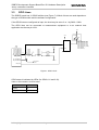
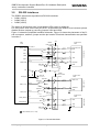
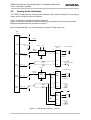
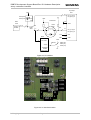
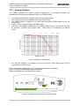
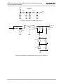
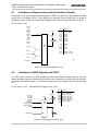
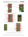
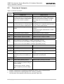
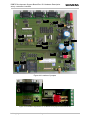
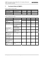
1
DSB75 Development Support Board Rev. B1 Version: DocID: v08 DSB75_hd_v08 Hardware Description s DSB75 Development Support Board Rev. B1 Hardware Description Strictly confidential / Released s Document Name: DSB75 Development Support Board Rev. B1 Hardware Description Version: v08 Date: September 29, 2005 DocId: DSB75_hd_v08 Status: Strictly confidential / Released General Notes Product is deemed accepted by Recipient and is provided without interface to Recipient’s products. The documentation and/or Product are provided for testing, evaluation, integration and information purposes. The documentation and/or Product are provided on an “as is” basis only and may contain deficiencies or inadequacies. The Documentation and/or Product are provided without warranty of any kind, express or implied. To the maximum extent permitted by applicable law, Siemens further disclaims all warranties, including without limitation any implied warranties of merchantability, completeness, fitness for a particular purpose and non-infringement of third-party rights. The entire risk arising out of the use or performance of the Product and documentation remains with Recipient. This Product is not intended for use in life support appliances, devices or systems where a malfunction of the product can reasonably be expected to result in personal injury. Applications incorporating the described product must be designed to be in accordance with the technical specifications provided in these guidelines. Failure to comply with any of the required procedures can result in malfunctions or serious discrepancies in results. Furthermore, all safety instructions regarding the use of mobile technical systems, including GSM products, which also apply to cellular phones must be followed. Siemens or its suppliers shall, regardless of any legal theory upon which the claim is based, not be liable for any consequential, incidental, direct, indirect, punitive or other damages whatsoever (including, without limitation, damages for loss of business profits, business interruption, loss of business information or data, or other pecuniary loss) arising out the use of or inability to use the Documentation and/or Product, even if Siemens has been advised of the possibility of such damages. The foregoing limitations of liability shall not apply in case of mandatory liability, e.g. under the German Product Liability Act, in case of intent, gross negligence, injury of life, body or health, or breach of a condition which goes to the root of the contract. However, Claims for Damages arising from a breach of a condition which goes to the root of the contract shall be limited to the foreseeable damage which is intrinsic to the contract, unless caused by intent or gross negligence or based on liability for injury of life, body or health. The above provision does not imply a change on the burden of proof to the detriment of the Recipient. Subject to change without notice at any time. The interpretation of this general note shall be governed and construed according to German law without reference to any other substantive law. Copyright Copying of this document and giving it to others and the use or communication of the contents thereof, are forbidden without express authority. Offenders are liable to the payment of damages. All rights reserved in the event of grant of a patent or the registration of a utility model or design. Copyright © Siemens AG 2005 DSB75_hd_v08 Page 2 of 94 29.09.2005 DSB75 Development Support Board Rev. B1 Hardware Description Strictly confidential / Released s Contents 0 Document History .........................................................................................................7 1 Introduction .................................................................................................................11 2 3 1.1 Supported Products .............................................................................................11 1.2 Related Documents .............................................................................................11 1.3 Scope of Delivery.................................................................................................12 1.4 Terms and Abbreviations.....................................................................................12 General Overview........................................................................................................14 2.1 Key Features at a Glance ....................................................................................14 2.2 System Overview .................................................................................................16 2.3 Location of Connectors, Switches, Jumpers, LEDs, Adjustable Resistors ..........17 2.4 Block Diagram .....................................................................................................18 2.5 Interface Overview...............................................................................................19 Description of DSB75 Interfaces ...............................................................................21 3.1 GSM Module Interface (Board-to-Board Connector) ...........................................21 3.2 Test Points...........................................................................................................23 3.3 GPIO Lines ..........................................................................................................25 3.4 SIM Card Interface...............................................................................................27 3.5 RS-232 Interfaces................................................................................................29 3.5.1 Serial Interface 1 (COM1) ......................................................................31 3.5.2 Serial Interface 2 (COM2) ......................................................................32 3.5.3 Debug Interface (COM3)........................................................................33 3.6 Analog Audio Interfaces.......................................................................................34 3.6.1 Audio Interface 1 (Handset) ...................................................................35 3.6.2 Audio Interface 2 (Headset or Speakerphone Operation)......................36 3.6.2.1 Recommended Headset ........................................................36 3.6.2.2 Speakerphone Operation.......................................................37 3.6.3 Microphone Circuit (Feeding Bridges) ...................................................38 3.7 Digital Audio Interface..........................................................................................39 3.8 USB Device Interface ..........................................................................................41 3.9 I²C Interface .........................................................................................................43 3.10 SD Card Interface ................................................................................................46 3.10.1 SD 4 Bit Mode........................................................................................48 3.10.2 SD 1 Bit Mode........................................................................................49 3.10.3 SPI Bus Mode ........................................................................................50 3.11 Serial Peripheral Interfaces .................................................................................51 3.12 Analog Interface...................................................................................................53 3.13 Antenna Interface ................................................................................................55 3.14 Power Supply Interfaces......................................................................................56 3.14.1 Internal Supply Voltages ........................................................................58 3.14.2 Power Supply for DSB75 and GSM Module ..........................................60 3.14.3 Battery Powered Operation of GSM Module..........................................61 3.14.3.1 Charging the Battery..............................................................61 DSB75_hd_v08 Page 3 of 94 29.09.2005 DSB75 Development Support Board Rev. B1 Hardware Description Strictly confidential / Released 3.14.4 3.14.5 4 5 6 4.1 Indication of Asynchronous Serial Interface Signals............................................66 4.2 Indication of GPIO Signals and SYNC.................................................................66 4.3 Indication of Power ..............................................................................................67 4.4 Indication of I²C Lines ..........................................................................................67 Overview of Switches and Jumpers..........................................................................68 5.1 Overview of Switches ..........................................................................................68 5.2 Overview of Jumpers ...........................................................................................73 Connecting Antenna and GSM Module to DSB75....................................................75 Turn on / off the GSM Module .............................................................................77 6.1.1 Turn on the GSM Module.......................................................................77 6.1.2 Turn off the GSM Module.......................................................................78 6.1.3 Emergency Restart ................................................................................78 Technical Data of DSB75............................................................................................79 7.1 8 3.14.3.2 Charging Circuit .....................................................................62 Real Time Clock Supply.........................................................................63 Adjusting the VBATT+ Supply Voltage for the GSM Module .....................64 Status LEDs .................................................................................................................65 6.1 7 s Cable Requirements ............................................................................................82 Appendix......................................................................................................................83 8.1 List of Parts and Accessories ..............................................................................83 8.2 Circuit Diagrams of DSB75..................................................................................84 8.3 Floor Plan of the DSB75 ......................................................................................93 Figures Figure 1: System overview ..................................................................................................... 16 Figure 2: Location of the connectors, switches, jumpers, LEDs and adjustable resistors...... 17 Figure 3: Block diagram ......................................................................................................... 18 Figure 4: Pin assignment of the B2B connector ..................................................................... 21 Figure 5: Overview of B2B connector pins and the corresponding test points....................... 23 Figure 6: Location of the test points ....................................................................................... 23 Figure 7: GPIO circuit............................................................................................................. 25 Figure 8: GPIO - location of switches and LEDs .................................................................... 26 Figure 9: SIM card interface ...................................................................................................27 Figure 10: Pin location of the Molex SIM card holder and test pins ....................................... 28 Figure 11: RS-232 interfaces ................................................................................................. 29 Figure 12: Location of the RS-232 interfaces and switches ................................................... 30 Figure 13: Recommended adapter cable from PC to COM2 on DSB75 ................................ 33 Figure 14: Analog audio interface – overview ........................................................................ 34 Figure 15: Location of the audio connectors and switches .................................................... 35 Figure 16: Siemens Car Kit Portable HKP-500 ...................................................................... 37 Figure 17: Circuit of microphone feeding bridges................................................................... 38 Figure 18: DAI interface ......................................................................................................... 39 DSB75_hd_v08 Page 4 of 94 29.09.2005 DSB75 Development Support Board Rev. B1 Hardware Description Strictly confidential / Released s Figure 19: Location of DAI connector X703 ........................................................................... 39 Figure 20: Example for connecting measurement equipment................................................ 40 Figure 21: USB device interface............................................................................................. 41 Figure 22: Location of the USB interface, switches and jumper............................................. 42 Figure 23: I²C interface........................................................................................................... 44 Figure 24: I²C interface location ............................................................................................. 44 Figure 25: SD card interface .................................................................................................. 46 Figure 26: Location of slide switches and card reader pins ................................................... 47 Figure 27: SPI interfaces........................................................................................................ 51 Figure 28: SPI interfaces location and related switches......................................................... 52 Figure 29 PWM filter characteristics....................................................................................... 53 Figure 30: Analog interface location and related switches ..................................................... 53 Figure 31: Analog interface ....................................................................................................54 Figure 32: Power supply interfaces ........................................................................................ 56 Figure 33: Location of the power supply connectors, switches and jumpers ......................... 57 Figure 34: Input circuit schematic (5V DC/DC converter) for power supply ........................... 58 Figure 35: Schematic for audio supply (5V0_I) ...................................................................... 59 Figure 36: Schematic for GSM module supply (3V3_4V5 or BATT+) .................................... 59 Figure 37: Battery screw terminal........................................................................................... 61 Figure 38: Schematic of charging circuit ................................................................................ 63 Figure 39: Location of jumpers and resistors for adjusting BATT+ voltage (3V3_4V5) ......... 64 Figure 40: Location of LEDs................................................................................................... 65 Figure 41: ASC signal indication circuit.................................................................................. 66 Figure 42: GPIO signal indication circuit ................................................................................ 66 Figure 43: Location, signal names and switch positions of the slide switches ....................... 72 Figure 44: Location of jumpers............................................................................................... 74 Figure 45: Illustration of positions to cut the trace for jumpers X203 and X122 ..................... 74 Figure 46: Mounting GSM module onto the DSB75 ............................................................... 75 Figure 47: Top view on DSB75 with connected GSM module and RF cable ......................... 76 Figure 48: Turn on circuit ....................................................................................................... 77 Figure 49: Schematic of page signals .................................................................................... 84 Figure 50: Schematic of position list....................................................................................... 85 Figure 51: Schematic sheet 1 – B2B connector, test points, USB interface .......................... 86 Figure 52: Schematic sheet 2 – ASC0, ASC1 and ASC2 interface........................................ 87 Figure 53: Schematic sheet 3 – SD card reader .................................................................... 88 Figure 54: Schematic sheet 4 – GPIOs, power supply........................................................... 89 Figure 55: Schematic sheet 5 – SIM card, I2C, SPI, analog and antenna interface .............. 90 Figure 56: Schematic sheet 6 – charging interface ................................................................ 91 Figure 57: Schematic sheet 7 – audio interface ..................................................................... 92 Figure 58: Floor plan top side.................................................................................................93 Figure 59: Floor plan bottom side........................................................................................... 94 Tables Table 1: Key features ............................................................................................................. 14 Table 2: Interfaces of the DSB75 ........................................................................................... 19 Table 3: Pin assignment of B2B connector X100................................................................... 22 Table 4: Pin assignment – B2B connector X100 and test points X101 .................................. 24 Table 5: Pin assignment – B2B connector X100 and test points X102 .................................. 24 Table 6: LED indication of GPIO status.................................................................................. 25 Table 7: GPIO assignment and switch position...................................................................... 26 Table 8: Pin assignment – SIM card holder X503 and test pins X501 ................................... 28 Table 9: Pin assignment of 1st serial interface COM1 (X201) ............................................... 31 DSB75_hd_v08 Page 5 of 94 29.09.2005 DSB75 Development Support Board Rev. B1 Hardware Description Strictly confidential / Released s Table 10: Pin assignment of 2nd serial interface COM2 (X202) ............................................ 32 Table 11: Pin assignment of debug interface COM3 (X205).................................................. 33 Table 12: Pin assignment of handset audio interface 1 (X502).............................................. 35 Table 13: Pin assignment of audio interface 2 (X700, X701) ................................................. 36 Table 14: Pin assignment of the USC/DAI interface X703 ..................................................... 40 Table 15: Pin assignment of USB device interface X110....................................................... 42 Table 16: Pin assignment of the I²C interface X511............................................................... 45 Table 17: Pin assignment of SD card interface X301 (SD 4 bit mode) .................................. 48 Table 18: Pin assignment of SD card interface X301 (SD 1 bit mode) .................................. 49 Table 19: Pin assignment of SD card interface X301 (SPI bus mode)................................... 50 Table 20: Alternative configuration of SPI interface lines....................................................... 51 Table 21: Pin assignment of the SPI interfaces X510 ............................................................ 52 Table 22: Pin assignment of the analog interface .................................................................. 54 Table 23: Description of power supply units........................................................................... 58 Table 24: Recommended specification of the laboratory PSU............................................... 60 Table 25: Connecting the laboratory PSU to X400 and X401 ................................................ 60 Table 26: Pin assignment of the screw terminal X602 ........................................................... 61 Table 27: Pin assignment of the X700 jack for the plug-in charger........................................ 62 Table 28: Pin assignment of the X701 jack for the plug-in charger........................................ 62 Table 29: Adjusting BATT+ voltage (3V3_4V5) ..................................................................... 64 Table 30: Overview of switch positions .................................................................................. 68 Table 31: Overview of jumpers............................................................................................... 73 Table 32: DSB75 maximum ratings........................................................................................ 79 Table 33: DSB75 technical data............................................................................................. 79 Table 34: List of parts and accessories.................................................................................. 83 DSB75_hd_v08 Page 6 of 94 29.09.2005 DSB75 Development Support Board Rev. B1 Hardware Description Strictly confidential / Released 0 s Document History Preceding document: "DSB75 Development Support Board Rev B1 Hardware Description", v07 New document: "DSB75 Development Support Board Rev. B1 Hardware Description" Version v08 Chapter What is new 3.6.2 Added description of EPREF. 3.6.2.2, 3.6.3 Added information about required bias voltage for speakerphone operations. 3.7 Table 14: Updated pin description of PCM interface. Preceding document: "DSB75 Development Support Board Rev B1 Hardware Description", v06 New document: "DSB75 Development Support Board Rev. B1 Hardware Description" Version v07 Chapter What is new 6.1.1 Modified section “Toggling low-high state of DTR”. 7 Table 33: DSB75 technical data: Added Ignition key, Emergency key, Ignition via DTR, Ignition via USB Preceding document: "DSB75 Development Support Board Rev B1 Hardware Description", v05 New document: "DSB75 Development Support Board Rev. B1 Hardware Description" Version v06 Chapter What is new 8.2 Figure 56: Schematic sheet 6 – charging interface – corrected value of R604 Preceding document: "DSB75 Development Support Board Rev B1 Hardware Description", v04 New document: "DSB75 Development Support Board Rev. B1 Hardware Description" v05 Chapter What is new 2.2 Modified Figure 2: Location of the connectors, switches, jumpers, LEDs and adjustable resistors 3.1 Corrected Table 3: Pin assignment of B2B connector X100 and Table 4: Pin assignment – B2B connector X100 and test points X101 Board-to-board connector X100 will be supplied by Molex 3.3 Added note that the status of GPIOs 1 – 6 and 9 – 10 will be indicated by LEDs. Deleted test pin X102 for connecting measurement equipment or an external application. Corrected Table 7: GPIO assignment and switch position 3.5.1 Table 9: Pin assignment of 1st serial interface COM1 (X201) – modified note on DTR line 3.11 Table 20: Alternative configuration of SPI interface lines – deleted GPIO as alternative interface Table 21: Pin assignment of the SPI interfaces X510 – corrected pin names 5.1 Table 30: Overview of switch positions – corrected the functions of several switches DSB75_hd_v08 Page 7 of 94 29.09.2005 DSB75 Development Support Board Rev. B1 Hardware Description Strictly confidential / Released s Preceding document: "DSB75 Development Support Board Rev B1 Hardware Description", v03 New document: "DSB75 Development Support Board Rev. B1 Hardware Description" v04 Chapter What is new 1.4 Updated table: “Terms and Abbreviations” 2.5 Deleted “for ORGA test device” in table 2, row “SIM” 3.3 Deleted line: “It is important to switch the used GPIO lines to the LED driver (S450 – S459 pos.3).” 3.6.2 Updated table 12. Added description for pin 1 – 8 (X700), pin 1 – 7, 9 (X701) 3.6.2.2 Added “The plug of “Siemens Car Kit portable HKP-500” is compatible to Lumberg connector X701. The plug of “Siemens Car Kit Portable” is compatible to Lumberg connector X700. Changed Siemens ordering number for HKP-500. 3.6.3 Modified figure: ”Circuit of microphone feeding bridges” 3.8 Corrected switch position for a direct connection of the USB lines to the GSM module. Table 14: deleted column “Remark” 3.9 Deleted section “I2C is a serial, 8-bit oriented data transfer bus for bit rates up to 400 kbps in Fast mode. It consists of two lines: the serial data line I²CDAT and the serial clock line I²CCLK. The electrical characteristics comply with the I²C standard.” Deleted section “A master is the device which initiates a data transfer on the bus and generates the clock signals to permit that transfer. At this time, any device addressed is considered a slave. The master can operate as a master transmitter or as a master receiver.” Changed: VEXT to VDD Modified figure: “I²C interface” Corrected table 15: Pin assignment of the I²C interface X511 3.10 Modified figures: “SD card interface” and “Location of slide switches” 3.11 Modified figure: “SPI interfaces” Corrected figure: “SPI interfaces location and related switches” 3.12 Deleted list item “The filter characteristic depends on the signal frequency range.” Added new figure: “PWM filter characteristics” Modified figures: “Analog interface” and “Analog interface location and related switches” 3.14 Modified figure: “Power supply interfaces” 3.14.1 Corrected Table 23, row “GSM module supply”: 4.7F to 4700µF. 3.14.3.2 Modified figure: “Schematic of charging circuit” 3.14.5 Replaced “slide switches” with “jumpers” Deleted constraints: “The maximum voltage is set only via the slide switches, it cannot be adjusted via the resistors. 4.1 Modified figure: “ASC signal indication circuit” 4.2 Modified figure: “GPIO signal indication circuit” 8.2 Added figures: “Schematic of page signals” and “Schematic of position list” Modified figure: “Schematic sheet 6 – charging interface” DSB75_hd_v08 Page 8 of 94 29.09.2005 DSB75 Development Support Board Rev. B1 Hardware Description Strictly confidential / Released s Preceding document: ”DSB75 Development Support Board Hardware Description", v02 New document: "DSB75 Development Support Board Rev. B1 Hardware Description" v03 Chapter What is new 2.2 Modified figure: “System overview” 2.3 Modified figure: “Placement of connectors, switches, jumpers, LEDs and adjustable resistors” 2.4 Modified figure: “Block diagram” 3.3 Modified figure: “GPIO circuit” 3.5.1 Corrected value of level converter D200 (COM1). Added information: “Therefore the PWR_IND signal is used for enabling and shut down converters.” 3.5.2, 3.5.3 Corrected value of level converter D201 (COM2, COM3). Added information: Therefore the PWR_IND signal is used for enabling and shut down converters. 3.6 Modified figure: “Analog audio interface – overview”; modified figure: “Location of the audio connectors and switches” 3.6.2.2 New speakerphone added. 3.8 Added information about second USB interface X111. Modified figure: “USB device interface”. 3.9 Added information about functionality of LEDs V503, V504. Modified figure: ”I²C interface”. 3.10 Modified figure: ”SD card interface” 3.12 Modified figure: ”Analog interface” 3.14 Modified figure: ”Power supply interface” 3.14.1 Modified information in Table 23, row “Power supply of digital part of DSB75”. Added new row in Table 23: “Digital IO supply (VDD)”” 3.14.2 Corrected information about power indication. 3.14.3 Changed information about battery operation. Added recommendations for batteries. 3.14.3.1 Added Siemens ordering number and technical data for plug-in charger. Added new table: “Pin assignment of the X701 jack for the plug-in charger”. 3.14.3.2 Corrected: Imax=150mV / 0.3Ohm = 500mA @ Jumper X600 open; Imax =150mV / 0.15Ohm =1A @ Jumper X600 closed Modified figure: “Schematic of charging circuit”. 3.14.4 New chapter: “Real Time Clock Supply” 4.2 Modified information about indication of GPIO signals. Modified figure: “GPIO signal indication circuit”. 4.3 Corrected information about indication of power. 4.4 New chapter: “Indication of I²C Lines” 5.1 Completely updated table: “Overview of switch positions”. 5.2 Table 31: added jumpers X122, X203, X204, X206, X420, X421 X562, X600 and footnotes 2, 3. Added figure: “Location of jumpers”. 6 Added mounting description and figure: “Mounting GSM module onto the DSB75”. 6.1.1 Deleted constraints: “Start-up by DTR0 toggling is only effective if the USB host is not active. Start-up by plugging the USB cable is only effective if the RS-232 lines are DSB75_hd_v08 Page 9 of 94 29.09.2005 DSB75 Development Support Board Rev. B1 Hardware Description Strictly confidential / Released Chapter s What is new deactivated by the host application (e.g. if the terminal program is closed). In later releases of DSB75 this problem will be solved.” Modified figure: “Turn on circuit”. 6.1.2 Added information about automatic restart of the module. 7 Updated technical data. 7.1 More detailed list of cable requirements. 8.2 Modified figures “Schematic sheet1” … “Schematic sheet7” 8.3 Modified figure: “Floor plan top side”; added figure: “Floor plan bottom side” Preceding document: ”DSB75 Development Support Board Hardware Description", v01 New document: ”DSB75 Development Support Board Hardware Description", v02 Chapter What is new Completely revised and updated all chapters and technical specifications. Added new chapters and appendix. DSB75_hd_v08 Page 10 of 94 29.09.2005 DSB75 Development Support Board Rev. B1 Hardware Description Strictly confidential / Released 1 s Introduction This document describes the DSB75 Development Support Board Rev. B1 The DSB75 Development Support Board is designed to assist system integrators in developing and evaluating products based on Siemens GSM modules. Furthermore, it is part of the Siemens reference equipment submitted for Type Approval GSM modules. This document describes all interfaces of the DSB75, provides technical specifications and presents guidelines for connecting and operating the GSM modules to be evaluated. At present, the DSB75 has not been approved to comply with the CE marking regulations and can be used for laboratory purposes only. Also, please note that the DSB75 and the connected GSM module are not ESD protected. Because of these current limitations, take care that the device is only used by authorized staff. Note: The document is only valid for the DSB75 Rev. B1. DSB75 Rev. A2 boards are no longer considered in the document. 1.1 Supported Products DSB75 comes as a universal evaluation kit for variety of different Siemens GSM modules. At present these are the following: MC75 TC63 TC65 The diversity of the supported products implies that, due to hardware or software specific properties, major differences occur regarding the availability of interfaces and the implementation of features. Therefore, please consult the specifications supplied with your module, especially [1] and [2], to make sure whether or not a described interface, signal, operating mode or function offered by the DSB75 is supported. 1.2 [1] [2] [3] Related Documents Hardware Interface Description of your GSM module AT Command Set of your GSM module Application 07: Rechargeable Lithium Batteries in GSM Applications DSB75_hd_v08 Page 11 of 94 29.09.2005 DSB75 Development Support Board Rev. B1 Hardware Description Strictly confidential / Released 1.3 Scope of Delivery Quantity 1.4 s Description 1 DSB75 Development Support Board 1 MiniMag antenna (850 MHz – 1990 MHz) 1 Adapter cable for MiniMag antenna 2 RF adapter cable 150mm 1 Votronic handset 2 Hexagon nuts (DIN 934 – ISO 4032) 2 Screws M2 (DIN 84 – ISO 1207) 2 Insulating spacers for M2, self-gripping Terms and Abbreviations Abbreviation Description ADC Analog-to-Digital Converter ASC Asynchronous Serial Controller B2B Board-to-Board connector CE Conformité Européene (European Conformity) CSD Circuit Switched Data CTS Clear to Send DAC Digital-to-Analog Converter DAI Digital Audio Interface DRX Discontinuous Reception DSB Development Support Board DSR Data Set Ready DTR Data Terminal Ready DTX Discontinuous Transmission EMC Electromagnetic Compatibility ESD Electrostatic Discharge GPIO General Purpose Input/ Output GPRS General Packet Radio Service GSM Global Standard for Mobile Communications IGT Ignition I/O Input/Output kbps kbits per second LDO Low Drop Out Regulator LED Light Emitting Diode DSB75_hd_v08 Page 12 of 94 29.09.2005 DSB75 Development Support Board Rev. B1 Hardware Description Strictly confidential / Released Abbreviation Description Li-Ion Lithium-Ion MMC Multi Media Card NTC Negative Temperature Coefficient PCB Printed Circuit Board PCM Pulse Code Modulation PSU Power Supply Unit PTT Push-To-Talk PWM Pulse Width Modulation RF Radio Frequency ROM Read-only Memory RTC Real Time Clock RTS Request to Send Rx Receive Direction SAR Specific Absorption Rate SCLK Serial Clock SD Secure Digital SELV Safety Extra Low Voltage SIM Subscriber Identification Module SMA RF connector system: SubMiniature version A SPI Serial Peripheral Interface Tx Transmit Direction USB Universal Serial Bus DSB75_hd_v08 s Page 13 of 94 29.09.2005 DSB75 Development Support Board Rev. B1 Hardware Description Strictly confidential / Released 2 General Overview 2.1 Key Features at a Glance s Table 1: Key features Feature Implementation GSM module interface • Direct connection and mechanical fixing of GSM module via 80-pin board-to-board connector and screws. Power supply • Laboratory PSU (9V…15V) or • Battery 3.3V…4.5V • Implemented charging circuit (FET) • Operation with plug-in charging adapter Antenna interface • Integrated connection between module’s Hirose connector and SMA connector SIM interface • SIM card connector with front tray loading and card detection • Supported SIM cards: 3V and 1.8V • SD card connector with front slot, card detection indication and write protection indication • Supply voltage: 2.9V • Supported modes: SD mode or SPI mode • Two analog audio interfaces (both with microphone supply) for connecting a handset, headset or speakerphone. • One digital audio interface (DAI) • Host mode • Supports 3V or 5V devices (configurable) • Connected I²C EEPROM (128kBit) with adjustable addresses SPI interface • Two interfaces to be used alternatively to other interfaces (option) • Host mode Serial interfaces • • Three RS-232C interfaces: COM1 - serial interface for data communication COM2 - serial interface for control purposes COM3 - serial interface for debug purposes Max. baud rate: 460800 bps • Autobauding at TBD bps USB interfaces • USB 1.1 Full Speed (12 Mbit/s) device interface at B receptacle (default) GPIOs • 10 GPIOs at pins • Switchable pull-up/down resistors (for 8 GPIO’s) • LED signaling (for 8 GPIO’s) Battery charging SD Card interface Audio interfaces I²C interface DSB75_hd_v08 Page 14 of 94 29.09.2005 DSB75 Development Support Board Rev. B1 Hardware Description Strictly confidential / Released Feature ADC inputs DAC output Signal indication Configuration facilities Temperature range Implementation • 2 analog inputs • Switchable loop with DAC output at each line • One analog output for DC or AC voltages • Filtered PWM signal • 23 LEDs are available for signal indication • Two LEDs for on/off indication • Several module signal lines have multiple functions (depending on the GSM module and its configuration). Those lines are switchable to the right interfaces by slide switches and jumpers. • Adjustable module supply voltage • Normal operation: 15°C to +35°C • Storage: -40°C and +85°C Size: 177mm x 160mm x 36mm (PCB) Physical characteristics • DSB75_hd_v08 s Page 15 of 94 29.09.2005 s DSB75 Development Support Board Rev. B1 Hardware Description Strictly confidential / Released System Overview PC COM3 (RS-232C) Debug interface ASC0 2 LEDs for I2C 12 LEDs for ASC0, ASC1 GSM module X501 80 Test points Audio interface 1 X503 Card holder Emergency restart SD card SIM card RF X100 B2B Flex cable (option) + Battery X602 SMA LED module On S420 Card holder X502 Ignition RF SIM test X301 RF cable V242 - V243, V450 - V455 - LED DSB On Measurement equipment X101,X102 D500 Battery connector V230 - V241 X505 I2C EEPROM DSB75 V503, V504 X506 Jumper X120, X121, X203, X405, X410, X411, X420, X421, X500, X710 S421 X400 X401 Power supply 9V...15V 8 LEDs for GPIOs I2C X110 USB B ASC2 RF cable SPI X205 X201 X202 ASC1 USB A USB device COM3 alternative module connection X703 COM1 X510 DAI interface X511 I2C device SPI1/2 device Digital aud io measurement equipment or codec Remote control Relay box COM2 COM1 (RS-232C) COM4 COM2 (RS-232C) Lab Power Supply Audio interface 2 or charging interface 2.2 V431 V430 Lumberg X700 or X701 RF or Handset GSM module Plug-in charger ORGA SIM test RF Antenna or GSM tester Figure 1: System overview DSB75_hd_v08 Page 16 of 94 29.09.2005 s DSB75 Development Support Board Rev. B1 Hardware Description Strictly confidential / Released 2.3 Location of Connectors, Adjustable Resistors Switches, X201 X202 Jumpers, LEDs, (X111 bottom side) X205 X110 X401 X400 X203 X120 S112 S5 01 S50 0 1 39 2 40 X101 S 455 S 456 S4 57 S46 0 S 461S4 62 S 450 S 451 S4 54 S 453 S4 52 V452 SD_D2 (GPIO3) SD_D1 (GPIO2) V453 SD_CLK (GPIO5) V455 SD_CMD (GPIO6) 1 3 1 3 C413 X410 X405 X411 X561 X560 X562 (1) 39 40 SD_D0 (GPIO1) R414 X 510 V 240 V23 8 3 3 V450 V451 (40) C414 1 2 X10² (80) R415 1 3 S111 1 3 X 551 1 X121 3 SD_D3 (GPIO4) X 552 1 1 X703 3 S110 1 3 V454 S5 04 X554 3 1 S 503 S200 3 V 239 V 241 V2 42 S201 1 S 502 X204 X 511 X206 not_used V457 not_used V456 I2CDAT V504 I2CCLK V503 RXD2_GPIO9 TXD2_GPIO10 V244 V 243 3 S 465 S 464 S 463 3 1 3 1 S 468 S 467 S 466 V23 0 V 234 V23 1 V 235 V23 2 V2 36 V23 3 V 237 1 S 458 S 459 S46 9 1 C415 S713 S712 3 X4 20 X 421 3 1 1 3 1 X122 X602 S301 S303 S305 S307 3 S601 S730 1 3 S731 1 3 1 3 S300 S302 S304 S306 S717 S716 1 1 3 X6 00 (41) X500 X501 S714 X710 S715 S710 X301 (bottom side) X502 S711 1 3 40 1 S4 2 0 S 421 X505 X100 80 41 X506 V431 V430 X700 X503 (X701 bottom side) Figure 2: Location of the connectors, switches, jumpers, LEDs and adjustable resistors DSB75_hd_v08 Page 17 of 94 29.09.2005 s DSB75 Development Support Board Rev. B1 Hardware Description Strictly confidential / Released 2.4 Block Diagram Test points 2x40 pole SIM /6 SIM 8 pin CCxxx SIM for future use USB-OTG Chip USB /3 USB_DN, USB_DP, VUSB_IN USB Mini A/B 3x VBUS_B USB B ASC2/GPIO /2 RXD2_GPIO9,TXD2_GPIO10 SD / GPIO /8 SD_xxx(GPIO1-6) SPICS, SPIDI Digital baseband processor SYNC /2 /1 ASC1 /4 SD_DET(GPIO8), SD_WP(GPIO7) PWR_IND I 8x EN /6 SDXX_I /2 SPI2_CS, SPI2_DI 11x SYNC VEXT /4 SD /2 SD /4 /4 ASC1 EN EN RTS0,CTS0,RING0,DCD0,DSR0,DTR0 RXD0,TXD0 SD SD /8 (RXD0,TXD0)_I I EN1 VDD /4 /4 SPI1/2 2x10pin RS232 ASC0 EN USC(1,2) USC(0:6) VDD /7 RS232 I EN2 I 2x USC SD-Card 4x 12x /6 ASC2 (Debug) SD_DET(GPIO8), SD_WP(GPIO7) RXD1, TXD1, RTS1, CTS1 RXD0 ... RING0 /2 VDD /6 10x PWR_IND /8 EN2 VDD /4 ASC0 SD I RS232 EN /2 DTR SD / GPIO 2x 5V SD SD /9 /7 DAI /2 I2CCLK, I2CDAT DAC (PWM) /1 DAC_OUT 10pin 5V I2C VDD SPI1_CS,SPI1_DI Level Shifter I2C 10pin ADC (MUX) /2 BATT+ /5 BATT+ Charge /1 VCHARGE Charge /3 CHARGEGATE, VSENSE, ISENSE Charge /1 BATTEMP Audio /1 Audio /1 ADC(1,2)_IN /1 EEPROM 2x 3V3-4V5 Battery 5V Feeding Bridge 5V Feeding Bridge /2 MIC2(N,P) Audio1 /2 EP2(N,P) ext. Supply /1 VEXT Audio2 /2 MIC1(N,P) Audio2 /2 EP1(N,P) 2x JP Switch TP_ENV Audio1 (Screw terminal) Charging VMIC AGND Analog baseband AGND Charger, AGND AGND EMC EMC Headset Handset EMRG_RST Reset /1 EMERG_RST On /1 IGT RTC Supply /1 VDDLP IGT BATT+ Adj. Reg. 3V3-4V5 LDO 3V0 DTR d/dt gn VBUS_B /8 VDD LDO PWR_IND /1 PWR_IND ge EN EN1 JP 80 pole B2B EN2 5V DC/DC 5V JP PSU 9V RF SD RF Cable GSM module Hirose SMA Figure 3: Block diagram DSB75_hd_v08 Page 18 of 94 29.09.2005 DSB75 Development Support Board Rev. B1 Hardware Description Strictly confidential / Released 2.5 s Interface Overview Table 2: Interfaces of the DSB75 Interface Reference number Description IGT S421 Ignition push button Emergency reset S420 Emergency reset push button Handset X502 Audio interface 1 (4-pin western jack). Intended for connecting a handset. SIM X503 SIM card holder RF X506 RF signal (SMA connector) Green LED V431 DSB ON. Power LED that indicates the operating voltage for the DSB75. Yellow LED V430 Module ON. Power LED that indicates the operating voltage for the GSM module. SD card X301 SD card holder Charger, X700, X701 Two different functions provided by the same connector (Lumberg connector): Headset, a) Input for plug-in charger Carkit b) Audio 2 interface for headset or speakerphone X700 for old, X701 for new Siemens accessories. 9V X400 (red) GND X401 (black) COM1 X201 Supply voltage nominal +9V. Connectors used to attach a laboratory PSU. Serial interface 1 (9-pin SubD connector). RS-232C interface with 8 data and modem control lines. Intended for GPRS data, circuit switched data, multiplexed data, AT commands. Connects to the module’s serial interface ASC0. COM2 X202 Serial interface 2 (9-pin SubD connector). RS-232C interface with 2 data and 2 modem control lines: TXD1 and RXD1 plus RTS1 and CTS1 for hardware handshake. Intended for GPRS data and AT commands. Connects to the module’s serial interface ASC1. COM3 X205 Debug interface (9-pin SubD connector). RS-232C interface with 2 data lines: TXD2 and RXD2. Connects to the module’s serial interface ASC2 (for Siemens internal use only). USB B X110, X111 USB device interface (type B receptacle) GSM module X100 80 pole board-to-board connector for GSM module RF X505 RF connector for connecting GSM module via RF cable Battery X602 Battery connector Test points X101, X102 80 test pins (80 pole dual strip1); 1:1 connection to B2B connector X100, Terminal for GPIO’s, ADCn_IN lines I²C X511 3V and 5V I²C interface (10 pole dual strip1) DSB75_hd_v08 Page 19 of 94 29.09.2005 DSB75 Development Support Board Rev. B1 Hardware Description Strictly confidential / Released Interface Reference number s Description SPI1/2 X510 SPI interface 1 and 2 (10 pole dual strip1) DAI X703 DAI (digital audio interface) Intended for digital audio measurements. SIM X501 SIM test interface (8 pole single strip1) Remote control X120, X121, X203, X405, X410, X411, X420, X421, X500, X710 Jumpers used to connect special PC controlled relay box. DAC filter X560 - X562 Jumpers used to insert a customized DAC filter. BATT+ current X122 Jumpers used for BATT+ current measurement. 1 Grid of the strip connectors: 0.1 inch DSB75_hd_v08 Page 20 of 94 29.09.2005 DSB75 Development Support Board Rev. B1 Hardware Description Strictly confidential / Released s 3 Description of DSB75 Interfaces 3.1 GSM Module Interface (Board-to-Board Connector) The Molex board-to-board connector X100 on the DSB75 is an 80-pin double-row receptacle. Figure 4 shows the names and positions of the pins on the DSB75. The pin allocation is identical to the GSM module, but pin names may be different. Several pins have multiple functions depending on the type of GSM module and alternate configuration. Figure 4: Pin assignment of the B2B connector DSB75_hd_v08 Page 21 of 94 29.09.2005 DSB75 Development Support Board Rev. B1 Hardware Description Strictly confidential / Released s Table 3: Pin assignment of B2B connector X100 Pin no. Signal name Signal name Pin no. 80 GND GND 1 79 DAC_OUT ADC1_IN 2 78 PWR_IND ADC2_IN 3 77 TP_ENV GND 4 76 RXD2_GPIO9 TXD2_GPIO10 5 75 SPICS SD_WP(GPIO8) 6 74 SD_3(GPIO4) SPIDI 7 73 SD_2(GPIO3) SD_DET(GPIO7) 8 72 SD_1(GPIO2) SD_CMD(GPIO6) 9 71 SD_0(GPIO1) SD_CLK(GPIO5) 10 70 I2CDAT I2CCLK 11 69 USB_DP VUSB_IN 12 68 USB_DN USC5 13 67 VSENSE ISENSE 14 66 VMIC USC6 15 65 EPN2 CCCLK 16 64 EPP2 VSIM 17 63 EPP1 CCIO 18 62 EPN1 CCRST 19 61 MICN2 CCIN 20 60 MICP2 CCGND 21 59 MICP1 USC4 22 58 MICN1 USC3 23 57 AGND USC2 24 56 IGT USC1 25 55 EMERG_RST USC0 26 54 DCD0 BATTEMP 27 53 CTS1 SYNC 28 52 CTS0 RXD1 29 51 RTS1 RXD0 30 50 DTR0 TXD1 31 49 RTS0 TXD0 32 48 DSR0 VDDLP 33 47 RING0 VCHARGE 34 46 VEXT CHARGEGATE 35 45 BATT+ GND 36 44 BATT+ GND 37 43 BATT+ GND 38 42 BATT+ GND 39 41 BATT+ GND 40 DSB75_hd_v08 Page 22 of 94 Note: The electrical characteristics of this interface meet the requirements of GSM module’s application interface. 29.09.2005 s DSB75 Development Support Board Rev. B1 Hardware Description Strictly confidential / Released 3.2 Test Points All module pins at the B2B connector X100 are connected 1:1 to pin headers X101, X102. They may be used for connecting measurement equipment, customized host interfaces or as access points to GPIOs, DAC, ADCs, audio lines, etc. 1 40 39 40 X101 1 39 2 40 1 2 X10² 41 80 1 40 X100 80 41 Figure 5: Overview of B2B connector pins and the corresponding test points 39 40 X101 1 39 2 40 X102 1 2 Figure 6: Location of the test points DSB75_hd_v08 Page 23 of 94 29.09.2005 DSB75 Development Support Board Rev. B1 Hardware Description Strictly confidential / Released s Table 4: Pin assignment – B2B connector X100 and test points X101 X100 pin number Signal name Signal name X100 pin number 80 GND 40 39 GND 1 79 DAC_OUT 38 37 ADC1_IN 2 78 77 PWR_IND 36 35 ADC2_IN 3 TP_ENV 34 33 GND 4 76 RXD2_GPIO9 32 31 TXD2_GPIO10 5 SPICS 30 29 SD_WP(GPIO8) 6 75 X101 test point SD_3(GPIO4) 28 27 SPIDI 7 73 SD_2(GPIO3) 26 25 SD_DET(GPIO7) 8 72 SD_1(GPIO2) 24 23 SD_CMD(GPIO6) 9 71 SD_0(GPIO1) 22 21 SD_CLK(GPIO5) 10 70 I2CDAT 20 19 I2CCLK 11 69 USB_DP 18 17 VUSB_IN 12 68 USB_DN 16 15 USC5 13 67 VSENSE 14 13 ISENSE 14 66 VMIC 12 11 USC6 15 65 EPN2 10 9 CCCLK 16 64 EPP2 8 7 VSIM 17 63 EPP1 6 5 CCIO 18 62 EPN1 4 3 CCRST 19 61 MICN2 2 1 CCIN 20 74 Note: The electrical characteristics of this interface meet the requirements of GSM module’s application interface. Table 5: Pin assignment – B2B connector X100 and test points X102 X100 pin number Signal name Signal name X100 pin number 60 MICP2 40 39 CCGND 21 59 MICP1 58 MICN1 38 37 USC4 22 36 35 USC3 23 57 AGND 34 33 USC2 24 56 IGT 32 31 USC1 25 55 EMERG_RST 30 29 USC0 26 54 DCD0 28 27 BATTEMP 27 53 CTS1 26 25 SYNC 28 52 CTS0 24 23 RXD1 29 51 RTS1 22 21 RXD0 30 50 DTR0 20 19 TXD1 31 49 RTS0 18 17 TXD0 32 48 DSR0 16 15 VDDLP 33 47 RING0 14 13 VCHARGE 34 46 VEXT 12 11 CHARGEGATE 35 45 BATT+ 10 9 GND 36 44 BATT+ 8 7 GND 37 43 BATT+ 6 5 GND 38 42 BATT+ 4 3 GND 39 41 BATT+ 2 1 GND 40 DSB75_hd_v08 X102 test point Page 24 of 94 29.09.2005 DSB75 Development Support Board Rev. B1 Hardware Description Strictly confidential / Released 3.3 s GPIO Lines The DSB75 board has 10 GPIO facilities (see Figure 7). Which of them are used depends on the type of GSM module and the software configuration. If the GPIO lines are configured as input, the level may be set to 0 or 1 by S460 - S469. The GPIO lines can be connected to measurement equipment or to an external host application via the test pin X101. 3V0 3V0 8x LED Buffer B2B X100 SD_DO(GPIO1) SD_D1(GPIO2) SD_D2(GPIO3) SD_D3(GPIO4) SD_CLK(GPIO5) SD_CMD(GPIO6) RXD2_GPIO9 TXD2_GPIO10 VDD 8 8 S450 S451 S452 S453 S454 S455 S458 S459 SD_WP(GPIO7) SD_DET(GPIO8) S460 S461 S462 S463 S464 S465 S468 S469 1 3 1 8x10K Enable V450 (GPIO1; SD_D0 ) V451 (GPIO2; SD_D1) V452 (GPIO3; SD_D2) V453 (GPIO4; SD_D3) V454 (GPIO5; SD_CLK) V455 (GPIO6; SD_CMD) V242 (GPIO9) V243 (GPIO10) D450, D221 8x10K 3 Test points X101 PWR_IND Figure 7: GPIO circuit GPIO status is indicated by LEDs (for GPIOs 1-6 and 9-10). Table 6: LED indication of GPIO status GPIO level LED status 0 (low) on 1 (high) off DSB75_hd_v08 Page 25 of 94 29.09.2005 s DSB75 Development Support Board Rev. B1 Hardware Description Strictly confidential / Released 1 V457 10 1 2 9 I2CDAT V504 I2CCLK V503 S455 S4 56 S457 V450 V451 V452 V456 S 500 X 511 9 S454 S4 53 S452 S450 S451 S460 S4 61 S462 S465 S464 S463 S468 S467 S4 66 S458 S4 59 S469 X 5 10 2 S 501 V 230 V 2 40 V 238 V 241 V 2 39 R XD 2_G P IO 9 V 242 T X 2_G P IO 1 0 V 2 43 1 V 24 4 S110 V 2 34 V 231 V 235 V 232 V 236 V 233 V 2 37 3 SD_D0 (GPIO1) SD_D1 (GPIO2) SD_D2 (GPIO3) V454 V453 SD_D3 (GPIO4) SD_CLK (GPIO5) V455 SD_CMD (GPIO6) 10 Figure 8: GPIO - location of switches and LEDs Table 7: GPIO assignment and switch position X100 pin 1 Signal name GPIO S450-459 S460-469 71 SD_D0 1 S450:3 S460:x1 72 SD_D1 2 S451:3 S461:x 73 SD_D2 3 S452:3 S462:x 74 SD_D3 4 S453:3 S463:x 10 SD_CLK 5 S454:3 S464:x 9 SD_CMD 6 S455:3 S465:x 8 SD_WP 7 6 SD_CD 8 76 RXD2_GPIO9 9 S458:3 S468:x 5 TXD2_GPIO1 0 10 S459:3 S469:x Switch position x may be position 1 or 3. high level input: x=1 low level input: x=3 Electrical characteristics are specified in section 7. DSB75_hd_v08 Page 26 of 94 29.09.2005 s DSB75 Development Support Board Rev. B1 Hardware Description Strictly confidential / Released 3.4 SIM Card Interface The DSB75 has an integrated SIM card interface. An appropriate SIM card (3V or 1.8V) is required to start the GSM module. The SIM card holder X503 placed on the DSB75 is from type Molex. To open the card holder simply press the yellow pin. In parallel to the SIM card holder X503, the test points X501 are connected, e.g. for SIM test equipment. In series to the recognition switch (holder pins 7 and 8) there is a jumper X500 connected. It must set for normal operation and may be used for testing the SIM card detection ability from a remote device. Figure 9 shows the simplified interface schematic. The pin location of the SIM card holder and SIM test pins is shown in Figure 10. The pin assignment is given in Table 8. SIM test pins CCGND VSIM CCRST CCIO CCCLK CCIN X501 Card holder B2B X100 4,5,7 1 2 6 3 8 X503 SIM card 4 1 21 17 CCGND VSIM 2 6 3 7 19 18 16 20 CCRST CCIO CCCLK CCIN X500 8 Figure 9: SIM card interface DSB75_hd_v08 Page 27 of 94 29.09.2005 DSB75 Development Support Board Rev. B1 Hardware Description Strictly confidential / Released s X500 1 X501 8 1 2 3 7 4 5 6 8 X503 Figure 10: Pin location of the Molex SIM card holder and test pins Table 8: Pin assignment – SIM card holder X503 and test pins X501 Pin number on holder X503 X501 test points Signal name I/O Function 1 1 VSIM O Supply voltage U = 2.93V (typ.) or 1.8V for SIM card, generated by the module. 2 2 CCRST O Chip card reset, prompted by the module 3 3 CCCLK O Chip card clock 4,8 4, 5, 7 CCGND - Separate ground line for the SIM card to improve EMC 5 - CCVPP - Not connected 6 6 CCIO I/O Serial data line, bi-directional 7 8 CCIN I Chip card detection 0 = Chip card drawer is inserted 1 = Chip card drawer is not inserted DSB75_hd_v08 Page 28 of 94 29.09.2005 s DSB75 Development Support Board Rev. B1 Hardware Description Strictly confidential / Released 3.5 RS-232 Interfaces The DSB75 offers three asynchronous RS-232 interfaces: • COM1 (ASC0) • COM2 (ASC1) • COM3 (ASC2) The status of all interface lines is indicated by LEDs (refer to section 4). For using ASCx lines on the test pins X101, X102 without the DSB75 level converter please disable receiver outputs by removing jumpers X204 and X206. Figure 11 shows the simplified interface schematic. Figure 12 shows the placement of the Dsub connectors, switches, jumper and the pin location. Electrical characteristics are specified in section 7. 3V0 9 pole D-sub X201 RS232 level converter D200 TXD0 USC2 RTS0,DTR0 3 32 1 ASC_SD 1 200 1 200 2 3 1 3 JP 49,50 2 JP PWR_IND 78 RXD1, CTS1 29,53 RXD2_GPIO9 TXD2_GPIO10 RTS,DTR GND DTR RS232 level converter D201 S303,307 9 pole D-sub X202 2,8 1 S302,306 3 2 2 200 2 2 200 RXD, CTS 3 1 S301,305 TXD1, RTS1 5 3V0 ASC_SD V200 200 EN d/dt V420 PWR_IND PWR_IND 56 TXD 7,4 X203 X204 IGT RXD SD S201 1 24 200 S300,304 1 3 3 31,51 1 76 S458 3,7 ASC_SD SD S459 2 1 200 1 200 3 1 3 JP PWR_IND TXD, RTS GND 9 pole D-sub X205 3 1 5 5 5 RXD TXD GND COM3 (ASC2) USC1 4 S200 1 25 8,6,1,9 CTS,DSR, DCD, RING 4 COM2 (ASC1) CTS0, DSR0, 52,48,54,47 DCD0, RING0 30 RXD0 COM1 (ASC0) B2B X100 EN X206 LED indication (0=on, 1=off) Figure 11: RS-232 interfaces DSB75_hd_v08 Page 29 of 94 29.09.2005 s DSB75 Development Support Board Rev. B1 Hardware Description Strictly confidential / Released Common COM1 (X201) COM2 (X202) X201 X202 6 9 1 6 5 COM3 (X205) X205 6 9 1 9 1 5 5 X203 1 X120 1 S455 S456 S457 S454 S453 S452 S450 S451 S460 S461 S462 S458 S459 S469 S468 S467 S466 3 S465 S464 S463 S110 1 2 X510 1 9 10 X562 39 40 X101 1 1 39 2 40 X551 X554 X552 S200 S502 S201 10 9 X703 10 S504 X511 9 1 2 S501 2 1 X204 S503 X206 1 S500 1 1 X561 1 X560 X102 1 2 S713 S712 S300 S302 S304 S306 S717 S716 S301 S303 S305 S307 S731 S730 Figure 12: Location of the RS-232 interfaces and switches DSB75_hd_v08 Page 30 of 94 29.09.2005 DSB75 Development Support Board Rev. B1 Hardware Description Strictly confidential / Released 3.5.1 s Serial Interface 1 (COM1) The 1st serial interface COM1 (X201) of the DSB75 is intended for the communication between the GSM module and the host application. This RS-232C interface is a data and control interface for transmitting data, AT commands and providing multiplexed channels etc. All modem status lines are available. A level converter D200 adapts and inverts the V.24 signals (2.9V level) from the GSM module to RS-232C level. The output lines are switched off (high impedance) while the GSM module is in POWER DOWN mode. Therefore the PWR_IND signal is used to enable and shut down converters. The rising edge of the DTR line voltage generates an ignition signal (impulse) via the V420 differential circuit so that it is possible to turn on the GSM module from the host, by plugging in the serial cable or by remote control. The USC lines (USC1, USC2) can be used as an alternative to the standard ASC0 lines (RXD0, TXD0). In this case the switches S200, S201 have to be set to position 3. The usability of the USC lines depends on the software configuration of the GSM module and is for Siemens internal use only. Table 9: Pin assignment of 1st serial interface COM1 (X201) X201 pin Name I/O 1 DCD O Data Carrier Detected DCD0 2 RXD O Receive Data RXD0 S200:1 USC1 S200:3 TXD0 S201:1 USC2 S201:3 3 4 TXD DTR I I Description Transmit Data Data Terminal Ready X100 signal name Config. switches Remark For Siemens internal use only For Siemens internal use only DTR0 Note: Low-to-high transition of the DTR line activates the ignition signal of the GSM module. 5 GND - Ground GND 6 DSR O Data Set Ready DSR0 Attention: Switch DSR0_I (X122) must be set to DSR0_I position. 7 RTS I Request To Send RTS0 8 CTS O Clear To Send CTS0 9 RING O Ring Indication RING0 DSB75_hd_v08 Page 31 of 94 29.09.2005 DSB75 Development Support Board Rev. B1 Hardware Description Strictly confidential / Released 3.5.2 s Serial Interface 2 (COM2) The 2nd serial interface COM2 (X202) of the DSB75 is intended for the communication between the GSM module and the host application. This RS-232C interface includes only the data lines RXD/TXD for transmitting GPRS data and AT commands, and the two control lines RTS/CTS. A level converter D201 adapts and inverts the V.24 signals (2.9V level) from the GSM module to the RS-232C level. The output lines are switched off (high impedance) if the GSM module is in POWER DOWN mode. Therefore the PWR_IND signal is used to enable and shut down converters. There are two alternative approaches to configure the ASC1 lines: • as SD card interface (see section 3.10.2) • as SPI interface (see section 3.10.3) For using ASC1 lines at the test pins X101/X102 without a RS-232 level shifter, the switches S300, S302, S304 and S306 have to be set to position 1. Table 10: Pin assignment of 2nd serial interface COM2 (X202) X202 pin Name I/O Description X100 signal name Config. switches 2 RXD O Receive Data RXD1 S302:3 S303:1 3 TXD I Transmit Data TXD1 S300:3 S301:1 5 GND - Ground GND 7 RTS I Request To Send RTS1 S304:3 S305:1 8 CTS O Clear To Send CTS1 S306:3 S307:1 1, 4, 6, 9 nc Remark nc= not connected DSB75_hd_v08 Page 32 of 94 29.09.2005 DSB75 Development Support Board Rev. B1 Hardware Description Strictly confidential / Released s As the X202 interface has only four lines, you may need a customized adapter cable for the RS-232 connection. This is useful, for example, if your application also requires the lines DSR, DCD, RING. In such a case it is recommended to use the following pin assignment: 9 pole Sub-D on DSB75 side (male) 9 pole Sub-D on PC side (female) 1 2 3 4 5 6 7 8 9 1 6 9 5 DCD RXD TXD DTR GND DSR RTS CTS RING RXD TXD GND RTS CTS 1 2 3 4 5 6 7 8 9 1 6 9 5 Figure 13: Recommended adapter cable from PC to COM2 on DSB75 3.5.3 Debug Interface (COM3) The debug interface COM3 (X205) of the DSB75 is reserved for Siemens internal software debugging. It is a two wire interface with data lines only. A level converter D201 adapts and inverts the V.24 signals (2.9V level) from the GSM module to RS-232C level. The output lines are switched off (high impedance) if the GSM module is in POWER DOWN mode. The ASC2 lines of the GSM module are used by default as GPIOs (see section 3.3) Table 11: Pin assignment of debug interface COM3 (X205) Pin Name I/O Description X100 signal name Config. switches 2 RXD O Receive Data RXD2_GPIO9 S458:1 3 TXD I Transmit Data TXD2_GPIO10 S459:1 5 GND - Ground GND 1, 4, 6, 7, 8, 9 nc Remark nc= not connected DSB75_hd_v08 Page 33 of 94 29.09.2005 s DSB75 Development Support Board Rev. B1 Hardware Description Strictly confidential / Released 3.6 Analog Audio Interfaces The DSB75 comprises two analog audio interfaces. Both audio interfaces are providing a supply circuit to feed an active microphone. Figure 14 shows the simplified interface schematic. Figure 15 shows the location of switches and the pin assignment of the audio connectors. Electrical characteristics are specified in section 7. Note: All specified data, e.g. load resistance are valid in TALK mode only. B2B X100 VMIC 3 66 S730 AGND 1 3 57 S731 1 AGND_I MICP1, MICN1 59,58 VMIC_I 2 S716,717 VMIC_I MICP1_I, MICN1_I 3 5V0 Western Jack X502 4 Feeding Bridge 1 Audio Interface 1: MICP + MICN 1 Handset AGND_I 3 EPP 6R8 EPP1, EPN1 63,62 2 S712,713 2 3 6R8 1 Lumberg X700 VMIC_I MICP2_I, MICN2_I MICP2, MICN2 60,61 2 S714,715 >=8 Ohm EPN 3 Audio Interface 2: 10 Feeding Bridge MICP 9 1 + AGND AGND_I Headset AGND_I 11 EPP 6R8 EPP2, EPN2 64,63 2 S710,711 12 3 EPN 6R8 Lumberg X701 1 12 11 AGND_I 10 8 MICP 32 Ohm or + AGND Headset EPP EPN 32 Ohm Figure 14: Analog audio interface – overview DSB75_hd_v08 Page 34 of 94 29.09.2005 s DSB75 Development Support Board Rev. B1 Hardware Description Strictly confidential / Released 1 S713 S712 X122 1 S300 S302 S304 S306 S717 S716 X602 S301 S303 S305 S307 X420 X421 1 1 1 1 X501 S240 X500 5 8 1 2 3 2 4 1 3 S421 S601 S730 S731 1 X710 S714 8 S715 1 S710 3 S711 X503 12 X100 X506 X502 V431 V430 1 X700 X701 (bottom side) 4 5 6 7 Figure 15: Location of the audio connectors and switches 3.6.1 Audio Interface 1 (Handset) This balanced interface has been optimized for use with the Votronic handset supplied with the DSB75. The Votronic handset is a passive handset. Power supply for its microphone is provided by the DSB75. The handset connects to the 4-pin Western jack X502. The pin assignment of the X502 jack is shown in Table 12. Table 12: Pin assignment of handset audio interface 1 (X502) Signal name Pin I/O Description MICN 1 I Microphone inverted EPN 2 O Loudspeaker inverted EPP 3 O Loudspeaker not inverted MICP 4 I Microphone not inverted The Votronic handset is the reference handset used with the DSB75. Acoustic approval of the Siemens DSB75 module applies to the reference configuration comprising the Votronic handset and the DSB75. GSM applications that incorporate audio devices other than the reference handset must be submitted for additional type approval. DSB75_hd_v08 Page 35 of 94 29.09.2005 DSB75 Development Support Board Rev. B1 Hardware Description Strictly confidential / Released 3.6.2 s Audio Interface 2 (Headset or Speakerphone Operation) The unbalanced audio interface 2 is designed for use with headsets or speakerphones. The interface is available on the 12-pin Lumberg connectors X700 and X701. The pin assignment of the Lumberg jacks is shown in Table 13. The power for the microphone (VMIC) is supplied by the GSM module. EPREF may be used for single ended loudspeaker configurations saving an additional coupling capacitor. Table 13: Pin assignment of audio interface 2 (X700, X701) Signal name X700 pin X701 pin I/O GND 1 2 - Ground Not relevant for audio. R 2 - 4.7k resistor to pin 3, necessary for old charger types. Not relevant for audio VCharge 3 1 I Supply voltage provided by the plug-in charger. Not relevant for audio n.c. 4, 6, 7, 8 3, 4, 6, 7 - Not connected. Not relevant for audio EPREF - 9 - 100µF capacitor to AGND. AC coupled loudspeaker ground GND 5 5 - 5kOhm to GND. AGND 9 11 - Microphone and stereo loudspeaker ground MICP 10 12 I Microphone not inverted. EPP 11 10 O Loudspeaker not inverted. EPN 12 8 O Loudspeaker inverted. 3.6.2.1 Description Recommended Headset A standard headset interface for mobile applications offered by Siemens is, for example, the PTT headset, ordering number L36880-N4001-A123 or Headset PTT HHS-510. Please note that the headset interface has no detections for a device plug or Push-To-Talk key (PTT). DSB75_hd_v08 Page 36 of 94 29.09.2005 DSB75 Development Support Board Rev. B1 Hardware Description Strictly confidential / Released 3.6.2.2 s Speakerphone Operation The recommended speakerphones which are currently available for the audio interface 2 are the “Siemens Car Kit Portable” and “Siemens Car Kit Portable HKP-500” (ordering number is L36880-N5601-A109). The plug of “Siemens Car Kit portable HKP-500” is compatible to Lumberg connector X701. The plug of “Siemens Car Kit Portable” is compatible to Lumberg connector X700. The required bias voltage for the MICP2 pin of the GSM module has to be achieved by an additional 2.2-kOhmresistor (see chapter 3.6.3, description of microphone interface 2). Figure 16: Siemens Car Kit Portable HKP-500 DSB75_hd_v08 Page 37 of 94 29.09.2005 DSB75 Development Support Board Rev. B1 Hardware Description Strictly confidential / Released 3.6.3 s Microphone Circuit (Feeding Bridges) This section describes the microphone signal path through feeding bridges. The location of the audio connectors can be seen in Figure 14. Figure 17 shows the principal circuit of microphone feeding bridges. The bridge for the audio interface 1 is optimized for feeding the Votronic headset. The balanced microphone is supplied with filtered 5V. The bridge for the unbalanced interface 2 is supplied directly from VMIC_I (2.5V). The GSM module requires a bias voltage of 1V…1.6V between MICP2_I and AGND_I. This is normally achieved by the voltage drop of the electret microphone in the case of headset operation. Please note for speakerphone operation, that no voltage drop occurs using the “Siemens Car Kit Portable” or “Siemens Car Kit portable HKP-500”. In this case an additional 2.2 kOhm resistor has to be connected between MICP2_I and AGND_I. It is recommended to connect this resistor between X102, pin 34 (AGND) and X102, pin 40 (MICP2). VMIC_I 4.7k 5V0_I 4.7k 2.2k 10µF MICP1_I 47k 10n X502 47k AGND_I MICP 100nF 600R/200MHz 1n MICN MICN1_I 600R/200MHz 100nF 10n 2.2k EMC-Filter VMIC_I 2.2k X700, X701 (Lumberg) 2.2k MICP2_I MICP 600R/200MHz MICN2_I 2.2nF 5.6k 2.2nF AGND AGND_I 600R/200MHz Figure 17: Circuit of microphone feeding bridges DSB75_hd_v08 Page 38 of 94 29.09.2005 DSB75 Development Support Board Rev. B1 Hardware Description Strictly confidential / Released 3.7 s Digital Audio Interface The Digital Audio Interface (DAI) can be used for acoustic approval or for transferring PCM digital audio data between the GSM module and the customer application. The DAI of the GSM module is designed for use with a codec or a DSP. The DSB75 provides different possibilities for connections between the GSM module and the system environment. This includes the 10 pin DAI connector X703 as well as the possibility to use the pin headers (X101, X102). Note: The DAI signals DAI0… DAI6 are connected to the signals USC0… USC6. The table below shows the pin assignment of the 10 pin DAI connector X703. Figure 18 shows the simplified interface schematic. Figure 19 shows the pin location of DAI connector. Electrical characteristics are specified in section 7. B2B X100 5V0 USC0 USC1 USC2 USC3 USC4 USC5 USC6 26 25 24 23 22 13 15 VDD 1 2 3 4 5 6 7 8 9 7 10 2x5 pin X703 5V0 2.9V DAI0 DAI1 DAI2 DAI3 DAI4 DAI5 DAI6 GND Figure 18: DAI interface 1 9 X703 2 10 Figure 19: Location of DAI connector X703 DSB75_hd_v08 Page 39 of 94 29.09.2005 s DSB75 Development Support Board Rev. B1 Hardware Description Strictly confidential / Released Table 14: Pin assignment of the USC/DAI interface X703 Signal name Pin PCM Interface Type Approval DAI I/O Remark I/O 5V0 1 O O VDD 2 O O DAI0 (USC0) 3 TXDAI O Clock 104kHz O DAI1 (USC1) 4 RXDAI I RX I DAI2 (USC2) 5 FS O TX O DAI3 (USC3) 6 BITCLK O Reset I DAI4 (USC4) 7 nc I Test1 I DAI5 (USC5) 8 nc I Test2 I DAI6 (USC6) 9 nc I Reset2 I GND 10 - - - - 5.0V supply for external circuit 2.9V supply for external circuit Optional: FS_OUT Ground DAI adapter X703 10 pole 25 pole D-Sub 5V0 1 DSB75 USC0 USC2 3 5 USC1 USC6 4 9 10 2x 2 e.g. 74HCT4050 2 2x 3k3 2x 6k8 24 23 25 22 12 GSM audio tester (e.g. R&S UPL16) with GSM 11.10 DAI interface Figure 20: Example for connecting measurement equipment DSB75_hd_v08 Page 40 of 94 29.09.2005 s DSB75 Development Support Board Rev. B1 Hardware Description Strictly confidential / Released 3.8 USB Device Interface DSB75 supports a USB 1.1 Full Speed (12 Mbit/s) device interface. It is primarily intended for use as command and data interface and for downloading firmware. The second USB interface with mini AB connector (X111) is reserved for future use and has been not described. Figure 21 shows the simplified interface schematic. Figure 22 shows the placement of the USB connectors, switches, jumper and the pin location. Electrical characteristics are specified in section 7. DSB75 provides a USB B receptacle to connect a host device. The USB lines VBUS, D+, Dare connected directly to the GSM module via slide switches S110 - S112 (position 3). In series to VBUS line there is a jumper (X120) connected. It is set during normal operation and may be used for remote control facilities. The rising edge of VBUS voltage generates an ignition signal (impulse) via the differential circuit V420. This way it is possible to turn on GSM module from the host, by plugging in the serial cable or by remote control. The EMC circuit protects the DSB75 and the GSM module against overvoltage (e.g. ESD). The USB I/O pins are capable of driving the signal at minimum 3.0V. They are protected from 5V input voltage driven from the host according to the USB specifications. B2B X100 IGT 56 d/dt V420 USB-B X110 Jumper VUSB_IN USB_DN USB_DP 12 68 69 S110 3 1 S111 S112 1 VBUS X120 EMC 2 3 1 3 3 1 4 D- D+ GND Figure 21: USB device interface DSB75_hd_v08 Page 41 of 94 29.09.2005 s DSB75 Development Support Board Rev. B1 Hardware Description Strictly confidential / Released X201 X205 X110 6 1 9 6 1 5 9 5 1423 X120 1 1 3 S455S456S457 S454S453S452 S450S451 S460S461S462 S465S464S463 S468S467S466 X400 1 1 S112 X121 1 S110 S458S459S469 X401 S111 Figure 22: Location of the USB interface, switches and jumper Table 15: Pin assignment of USB device interface X110 X110 pin Name I/O Description X100 signal name Config. switches 1 VBUS I (Supply) USB bus voltage VUSB_IN S110:3 2 D- Diff. I/O Data line minus USB_DN S111:3 3 D+ Data line plus USB_DP S112:3 4 GND GND GND DSB75_hd_v08 Supply Page 42 of 94 29.09.2005 DSB75 Development Support Board Rev. B1 Hardware Description Strictly confidential / Released 3.9 s I²C Interface The GSM module is the bus master device. The I2CDAT and I2CCLK lines have to be connected on the slave side to a positive supply voltage via a current source or pull-up resistor. The number of interfaces connected to the bus is only dependent on the bus capacity limit of 400pF. Each device connected to the bus is software addressable by a unique address, and simple master/slave relationships exist at all times. On the DSB75 both I²C lines can alternatively be used as SPI interface lines (if supported by the GSM module, see section 3.11). The I²C interface lines are available on the DSB75 at the 10 pin header X511. A level shifter V500/V501 converts from 3V up to 5V logic. The 3V logic lines are connected directly to the pins of the pin header X511, if switches S500 and S501 are set to position 1. Attention: Two external pull-up resistors must be installed in the host application. There are no on-board pull-up resistors. The 5V compliant lines are an alternative to the 3V lines available on the X511 pin header. To use 5V lines, set the switches S500 and S501 to position 3. The two logic voltages 5V0 and VDD are available at the X511 pin header for supplying the external I²C device driver. For a simple test facility a 128kBit EEPROM device (D500) with adjustable address area (S502 - S504) is implemented. Accordingly the switches S500 and S501 are set to position 3 (see Figure 23). The LED V503 indicates that I2CCLK line is active (low). The LED V504 indicates that I2CDAT line is active (low). Figure 23 shows the simplified interface schematic. Figure 24 shows the placement of the I²C switches and the pin location. Electrical characteristics are specified in section 7. DSB75_hd_v08 Page 43 of 94 29.09.2005 s DSB75 Development Support Board Rev. B1 Hardware Description Strictly confidential / Released 10 pole pin X511 VDD 2 V504 (DAT) V503 (CLK) 5V 0 VDD 0=on 1=off level shifter: B2B X100 I2CCLK, I2CDAT 11,70 1 2 S500, S501 3 2,4 3k3 8,10 GND V500/ V501 3k3 2 2 1,3 5V0 D500 2 VDD 7 I2C_CLK_5V, I2C_DAT_5V 5V0 9 VDD VDD SCL,SDA A(0:2) I2C_CLK_3V, I2C_DAT_3V Address 3 3 1 EEPROM 128kBit S502 (A0), S503 (A1), S504 (A2) AT24C128N V504 V503 Figure 23: I²C interface S501 S504 S503 S502 S500 2 1 10 X511 9 Figure 24: I²C interface location DSB75_hd_v08 Page 44 of 94 29.09.2005 DSB75 Development Support Board Rev. B1 Hardware Description Strictly confidential / Released s Table 16: Pin assignment of the I²C interface X511 X511 pin Name I/O Description X100 signal name Config. switches Remark 1 I2C_CLK_5V O Clock, (5V logic) I2CCLK S500:3 EEPROM accessible 2 I2C_CLK_3V O Clock, (3V logic) I2CCLK S500:1 External pull-up resistor required 3 I2C_DAT_5V I/O Data, (5V logic) I2CDAT S501:3 EEPROM accessible 4 I2C_DAT_3V I/O Data, (3V logic) ISCDAT S501:1 External pull-up resistor required 5 n.c. 6 n.c. 7 5V0 O 5V0 supply voltage 8 GND 9 VDD 10 GND DSB75_hd_v08 ON when DSB75 is supplied Ground O 2.9V supply voltage ON when GSM module is active Ground Page 45 of 94 29.09.2005 s DSB75 Development Support Board Rev. B1 Hardware Description Strictly confidential / Released 3.10 SD Card Interface The SD card interface provides a card reader for SD (Secure Digital) memory cards. It has a smooth push-push mechanism with front cover retention for temper-resistant card insertion. There are two contacts for card detection and write protect detection. The SD card interface can be operated in three modes: • SD 4 bit mode • SD 1 bit mode • SPI bus mode The supported operation mode depends on the type of GSM module and the selected configuration (see subsections 3.10.1, 3.10.2 and 3.10.3). Each mode has to be set and configured on the DSB75 by slide switches. Figure 25 shows the simplified interface schematic. Figure 26 shows the location of card reader pins and slide switches. Electrical characteristics are specified in section 7. B2B X100 4) 8 10 S450-455 SD_xx N412 71-74,10,9 1 6 3 47k 8 8 7 7 6 6 5 5 4 4 3 3 2 2 SD_D3_I 1 1 SD_D2_I 9 9 SD_D1_I SD_D0_I SD_CLK_I VDD alternative SD_CMD_I 3 ASC1 1) 53,51,31,29 4 3 1 1 S301,303, S305,307 3) card detect SD_D0_I write protect slide DAT1 unlock SD_DET 11 lock SD_WP X301 6 DAT0 GND 2) CLK VDD GND 50k CMD CD/DAT3 DAT2 SD Card SD_CLK_I SD card holder SD_CMD_I SD_D3_I 1) ASC1= TXD1, RXD1, RTS1, CTS1 2) Internal switch is closed after power up and open during regular data transfer, used for card detection, if GPIO8 not available for card detection. 3) Card detect switch is closed when card is inserted. 4) Write protect switch is closed when card is unlocked or MMC is inserted. S300,302 S304,306 Figure 25: SD card interface DSB75_hd_v08 Page 46 of 94 29.09.2005 s DSB75 Development Support Board Rev. B1 Hardware Description Strictly confidential / Released 1 S455S456S457 S454S453S452 S450S451 S460S461S462 X510 S465S464S463 S458S459S469 2 1 S468S467S466 S110 3 9 10 39 40 1 1 39 2 40 X101 X551 S501 X562 X552 S200 S504 S201 S502 9 10 9 1 X703 X554 10 2 S503 S500 X511 1 2 1 X561 1 X560 X102 1 2 S713S712 S717S716 S300S302S304S306 S301S303S305S307 S731 S730 1 X500 11 10 8 7 6 5 4 3 2 1 9 X301 Figure 26: Location of slide switches and card reader pins DSB75_hd_v08 Page 47 of 94 29.09.2005 s DSB75 Development Support Board Rev. B1 Hardware Description Strictly confidential / Released 3.10.1 SD 4 Bit Mode Table 17: Pin assignment of SD card interface X301 (SD 4 bit mode) X301 pin 1 X301 signal name CD/DAT3 I/O I/O Description Data line bit 3, Card detect Remark Card detect at power on: 0 or open = card removed 1 or 50k pull-up = card inserted X100 signal name SD_D3 Configuratio n switches S453:1 S301:1 Note: This is no removal detection during card operation! 2 CMD O Command / Response SD_CM D GND 3 VSS1 Supply Ground 4 VDD Supply Supply voltage 2.9V 5 CLK O Clock 25.4kHz …13MHz (depends on SW performance) SD_CLK S455:1 S303:1 S454:1 S305:1 6 VSS2 Supply Ground GND 7 DAT0 I/O Data line bit 0 SD_D0 S450:1 S307:1 8 DAT1 I/O Data line bit 1 SD_D1 S451:1 9 DAT2 I/O Data bus bit 2 SD_D2 S452:1 10 CD I Card detection 0 = card inserted 1 = card removed SD_DET Note: On each edge an interrupt will be generated. Removing the card will stop its operation before disconnecting it. 11 WP DSB75_hd_v08 I Write protect detection 0 = unlocked 1 = locked Page 48 of 94 SD_WP 29.09.2005 s DSB75 Development Support Board Rev. B1 Hardware Description Strictly confidential / Released 3.10.2 SD 1 Bit Mode Table 18: Pin assignment of SD card interface X301 (SD 1 bit mode) X301 pin X301 signal name 1 - I/O I/O Description Remark Not used X100 signal name SD_D3 Configuratio n switches S453:3 S301:1 2 CMD O Command / Response SD_CM D GND 3 VSS1 Supply Ground 4 VDD Supply Supply voltage 2.9V 5 CLK O Clock 25.4kHz …13MHz (depends on SW performance) SD_CLK S455:1 S303:1 S454:1 S305:1 6 VSS2 Supply Ground GND 7 DATA I/O Data line SD_D0 S450:1 S307:1 8 - Not used 9 - Not used 10 CD I Card detection 0 = card inserted 1 = card removed SD_DET Note: On each edge an interrupt will be generated. Removing the card will stop its operation before disconnecting it. 11 WP DSB75_hd_v08 I Write protect detection 0 = unlocked 1 = locked Page 49 of 94 SD_WP 29.09.2005 s DSB75 Development Support Board Rev. B1 Hardware Description Strictly confidential / Released 3.10.3 SPI Bus Mode This interface is an option and an alternative to the ASC1 and SPI2 interfaces. It has to be reconfigured via AT commands as SPI bus mode SD card interface. For further information refer to section 3.11. Table 19: Pin assignment of SD card interface X301 (SPI bus mode) X301 pin X301 signal name 1 CS I/O O Description Chip select Remark Active low X100 signal name TXD1 Configuratio n switches S300:3 S301:3 S453:3 2 DI I Data input Data out (DO) at SD card side CTS1 S306:3 S307:3 S450:3 3 VSS1 Supply Ground GND 4 VDD Supply Supply voltage 2.9V 5 SCLK O Clock up to 3.25MHz RTS1 S304:3 S305:3 S454:3 6 VSS2 Supply Ground 7 DO O Data output GND Data in (DO) at SD card side RXD1 S302:3 S303:3 S455:3 8 - Not used 9 - Not used 10 CD I Card detection 0 = card inserted 1 = card removed SD_DET Note: On each edge an interrupt will be generated. Removing the card will stop its operation before disconnecting it. 11 WP DSB75_hd_v08 I Write protect detection 0 = unlocked 1 = locked Page 50 of 94 SD_WP 29.09.2005 s DSB75 Development Support Board Rev. B1 Hardware Description Strictly confidential / Released 3.11 Serial Peripheral Interfaces The Serial Peripheral Interface (SPI) system consists of one master device and one or more slave devices. The master is defined as a microcomputer providing the SPI clock, and the slave as any integrated circuit receiving the SPI clock from the master. The GSM module always operates as a master device in master-slave operation mode. The SPI has a 4-wire synchronous serial interface. Data communication is enabled with a low active Slave Select or Chip Select wire (CS). Data are transmitted with a 3-wire interface consisting of wires for serial data input (DI), serial data output (DO) and serial clock (SCLK). The GSM module may provide two different SPI interfaces available alternatively to the I²C-, and ASC1- lines (depending on software configuration). On the DSB75, they are available on the 10 pin X510 pin header. In order to use the SPI interfaces some switches have to be set (see Figure 27). The logic voltage VDD is available at the X510 pin header for the supply of the external SPI device driver. Table 20: Alternative configuration of SPI interface lines SPI interfaces SPI1 Alternative interfaces CS1 DI1 DO1 I2C I2CDAT SCLK1 SPI2 CS2 I2CCLK ASC1 TXD1 DI2 RXD1 DO2 CTS1 SCLK2 RTS1 Figure 27 shows the simplified interface schematic. Figure 28 shows the placement of the SPI related switches and the pin location. Electrical characteristics are specified in section 7. B2B X100 TXD1 RXD1 RTS1 CTS1 SPICS SPIDI I2CCLK I2CDAT 31 29 51 53 75 7 11 70 4 S300 S302 S304 S306 10 pin X510 4 1 3 4 S456 S457 S500 S501 4 1 3 VDD 1 3 5 7 CS2 DI2 SCLK2 DO2 2 4 6 8 CS1 DI1 SCLK1 DO1 9 10 SPI2 SPI1 VDD GND Figure 27: SPI interfaces DSB75_hd_v08 Page 51 of 94 29.09.2005 s DSB75 Development Support Board Rev. B1 Hardware Description Strictly confidential / Released S455S456S457 S454S453S452 S450S451 X510 S460S461S462 2 1 S465S464S463 S458S459S469 3 S468S467S466 S110 1 9 10 9 1 X703 10 2 S501 X562 39 40 1 39 2 40 X101 1 X551 X554 X552 S200 S504 S201 S502 9 10 S503 S500 X511 1 2 1 X561 1 X560 1 2 X10² S713S712 S717S716 S300S302S304S306 S301S303S305S307 Figure 28: SPI interfaces location and related switches Table 21: Pin assignment of the SPI interfaces X510 X510 pin Name I/O Description X100 signal name Config. switches 1 CS2 O Chip select 2 TXD1 S300:1 2 CS1 O Chip select 1 SPICS S456:1 3 DI2 I Data in 2 RXD1 S302:1 4 DI1 I Data in 1 SPIDI S457:1 5 SCLK2 O Clock 2 RTS1 S304:1 6 SCLK1 O Clock 1 I2CCLK S500:1 7 DO2 O Data out 2 CTS1 S306:1 8 DO1 O Data out 1 I2CDAT S501:1 9 VDD O 2.9V supply out 10 GND DSB75_hd_v08 Page 52 of 94 Remark 29.09.2005 s DSB75 Development Support Board Rev. B1 Hardware Description Strictly confidential / Released 3.12 Analog Interface The DSB75 provides an analog interface allowing you to efficiently evaluate the characteristics of the analog baseband codec of the GSM module: • • • • • This analog interface has 2 analog inputs and one analog output. The analog input lines are available on the pin header X101. The analog output is available as a pulse width modulation (PWM) signal on the pin header X101. A filter circuit 2nd order smoothes the PWM signal. The filter on the DSB75 is optimized for 8.125kHz PWM frequency and can be removed by customer. Therefore the jumpers X560 - X562 have to be replaced by customer circuit. 0,1 1 10 100 1000 10000 100000 0 -10 Filter attenuation [dB] -20 -30 -40 -50 -60 -70 -80 -90 PWM frequency [Hz] Figure 29 PWM filter characteristics • For self test facilities it is possible to turn on test loops. Each analog input can be connected to the filter output. X562 39 40 X101 1 1 39 2 40 1 X551 X552 S501 S503 S200 9 1 X703 X554 10 2 S504 S201 S502 9 10 S500 X511 Figure 30 shows the placement of the related switches and the pin location. Figure 31 shows the simplified interface schematic. Electrical characteristics are specified in section 7. 3 1 X561 1 X560 X102 1 2 Figure 30: Analog interface location and related switches DSB75_hd_v08 Page 53 of 94 29.09.2005 s DSB75 Development Support Board Rev. B1 Hardware Description Strictly confidential / Released Test point strips X101 B2B X100 79 DACOUT 38 Filter: 41 GND 40 GND 2 X560 1 2 X561 X562 3 3 1 X551 DACOUT_F DACOUT_F 1 1 X552 2 37 3 35 57 34 AD1_IN AD2_IN AGND DACOUT AD1_IN AD2_IN AGND Figure 31: Analog interface Table 22: Pin assignment of the analog interface Pin Name I/O Description X100 signal name Switch setting for loop Remark X101/37 AD1_IN I ADC Input 1 AD1_IN X551:3 X101/35 AD2_IN I ADC Input 2 AD2_IN X552:3 If no loop required Keep switches in position 1 X101/34 AGND Ground for ADC Inputs AGND X101/38 DACOUT O DAC Output (PWM) DACOUT X561/1 DACOUT_F O DAC Output (filtered) DACOUT X101/40 GND DSB75_hd_v08 If no loop required: Jumper bridge X561 can be removed Ground for DAC Output Page 54 of 94 29.09.2005 DSB75 Development Support Board Rev. B1 Hardware Description Strictly confidential / Released 3.13 s Antenna Interface The RF signal of the GSM module is connected via the supplied RF adapter cable to the Hirose RF jack X505 located on the DSB75. Furthermore, in order to send or receive data, connect an external RF antenna to the SMA jack X506 which is internally connected to the Hirose RF connector X505. To obtain optimum send and receive performance, a steel grounding plate (at least 300mm x 300mm) should be placed underneath the antenna. Please consider that the supplied antenna equipment has been chosen to achieve optimum RF performance when operating the GSM module at the DSB75. Siemens does not accept warranty claims for damage caused by inappropriate equipment connected to the antenna connectors. Electrical characteristics are specified in section 7. DSB75_hd_v08 Page 55 of 94 29.09.2005 s DSB75 Development Support Board Rev. B1 Hardware Description Strictly confidential / Released 3.14 Power Supply Interfaces The constant voltage supply on the PCB provides all the supply voltages required for operating DSB75 and the GSM module. The power supply source can be a 9V…15V laboratory PSU or mains adapter and, in addition, an external battery used to feed only the GSM module. The DSB75 has three power supply interfaces: • Interface X400/X401 – connects to a laboratory PSU for supplying the DSB75 itself and the connected GSM module. See section 3.14.2. • Interface X602 (screw terminal block) - connects to an external battery for supplying only the GSM module, while DSB75 is powered from the laboratory PSU. See section 3.14.3. • Interface X700 or X701 (Lumberg connector) – input for charging the battery. See section 3.14.3.1. The S601 toggle switch selects whether to feed the GSM module from the laboratory PSU or a battery. If no battery is connected the S601 switch must be flipped down to supply voltage (BATT+) for the GSM module. Vice versa, if a battery is present, it must be flipped up. Figure 32 shows the simplified power supply interfaces schematic. Figure 33 shows the placement of the power supply connectors, switches, jumpers and the pin location. 5V0 N412 LDO PWR_IND VDD (2.9V) EN V200 N400 + PSU 9-15V - red X400 black - 5.0V-8V 5.0V DC LDO 3V0 DC X401 X700 Charger + N411 PWR_IND 1 3 X701 - X405 2 4 41-45 V60x, N600 6 X710 S601 5V0 4,5 33 100µF + adj. 3V3_4V5 S601 regulator 3 SD 1 1 + VBAT Charging circuit 3 34 35 14 67 27 1,2 Battery 78 N410 B2B X100 PWR_IND VDDLP BATT+ VCHARGE CHARGEGATE ISENSE VSENSE BATTEMP X602 Figure 32: Power supply interfaces DSB75_hd_v08 Page 56 of 94 29.09.2005 DSB75 Development Support Board Rev. B1 Hardware Description Strictly confidential / Released s X110 1423 X401 X400 1 1 X120 S112 X121 1 S111 N400 C413 V 601 N410 V 602 X410 X405 1 1 1 X411 V 600 N6 00 C414 C415 1 X122 1 X602 S601 5 1 X710 S714 S715 X505 S710 TP105 S711 1 12 TP106 X506 V431 V430 X700 Figure 33: Location of the power supply connectors, switches and jumpers DSB75_hd_v08 Page 57 of 94 29.09.2005 s DSB75 Development Support Board Rev. B1 Hardware Description Strictly confidential / Released 3.14.1 Internal Supply Voltages This section describes the internal supply voltages generated by the power supply unit of DSB75. A simplified block diagram of the power supply concept is shown in section 3.14. Table 23: Description of power supply units Power Supply Unit Description General supply 5V0 (see Figure 34) DSB75 accepts an input voltage between 9V and 15V DC on jacks X400 and X401. These ports are protected against polarity reversal by a simple diode V400. To reduce power dissipation, a DC/DC converter N400 provides a constant voltage of 5.0V. This voltage is used for supplying 3 LDOs and the audio section with power and is available for battery charging, supplying I2C and DAI interface. Audio supply (5V0_I) (see Figure 35) Audio power supply is decoupled with simple low pass filters from 5V0 supply. GSM module supply (3V3_4V5 or BATT+) (see Figure 36) For supplying the GSM module with regulated voltage the toggle switch S601 must be flipped down. In addition, the LDO for battery voltage N410 is adjustable for three voltage values (please refer to Table 29 and Figure 39). Two capacitors at 4700µF suppress voltage drops and ripples at GSM burst. For remote control, the jumper X405 has to be set to shut down the voltage. Power supply to digital part of DSB75 (3V0) (see Figure 32) The simple LDO (N411) regulates the 5V0 voltage down to 3.0V. Digital IO supply (VDD) (see Figure 32) The simple LDO (N412) regulates the 5V0 voltage down to 2.9V but this voltage is enabled by inverted PWR_IND signal. Therefore VDD is only present when the GSM module is operating. This voltage supplies the digital devices (RS232 driver, LED-driver). This voltage supplies the digital IO pull-up resistors, EEPROM, SD card and the digital interfaces: I²C, SPI, DAI. 3N3 C402 8K25 LM2596S-ADJ 2-POL 2 47U 2 5 1 2 GND1 GND2 V400 1 X401 OUT 1 C400,401,405 3 6 N400 V401 2-POL 1SR154-400 2 1 2 X400 ZJYS51R5-2PT 4 40V/1A 1 R401 2K7 R400 5V0 C403,410,413 470,473 L401 4812µF 661µF L400 GND GND GND GND GND Figure 34: Input circuit schematic (5V DC/DC converter) for power supply DSB75_hd_v08 Page 58 of 94 29.09.2005 s DSB75 Development Support Board Rev. B1 Hardware Description Strictly confidential / Released 5V0 GND GND GND 100µF 5V0_I C753 C752 R751 100µF R750 C751 100R 100N 100R C750 100N AUDIO GND Figure 35: Schematic for audio supply (5V0_I) SD GND 3 5 ADJ 3V3_4V5 N410 C412,414,415 C411 1 4 VOUT R410 R409 LP3856-ADJ 1N 10K 2 5V0 VIN 2K7 2 9410µF 1 X405 GND 2 R414 R411 GND 1K GND 2 R415 1 1K X410 1 1K X411 GND Figure 36: Schematic for GSM module supply (3V3_4V5 or BATT+) DSB75_hd_v08 Page 59 of 94 29.09.2005 DSB75 Development Support Board Rev. B1 Hardware Description Strictly confidential / Released 3.14.2 s Power Supply for DSB75 and GSM Module The voltage provided by the 9V…15V PSU generates all supply voltages required for the DSB75 and the connected GSM module when battery operation is disabled. The output power of the laboratory PSU has to satisfy the SELV requirements in accordance to EN 60950. Table 24: Recommended specification of the laboratory PSU Parameters Value Unit Min. Typical Max. Output voltage 8.5 12 15.5 Output current 1.5 V A Table 25: Connecting the laboratory PSU to X400 and X401 Voltage Connector Color Supply voltage +9V…+15V 4 mm PCB jack Red (X400) Ground 4 mm PCB jack Black (X401) If no battery is present and the GSM module is powered from the laboratory PSU be sure that the S601 toggle switch is in down position. The green LED (V431) on the DSB75 is driven by 3V0 voltage and indicates that the DSB75 is supplied with power and switched on. See also 4.3. DSB75_hd_v08 Page 60 of 94 29.09.2005 s DSB75 Development Support Board Rev. B1 Hardware Description Strictly confidential / Released 3.14.3 Battery Powered Operation of GSM Module - 1 Battery Battery Connector The external battery connects to the screw terminal block X602 (see Figure 37). 3 5 + X602 Figure 37: Battery screw terminal For battery operation, the toggle switch S601 must be flipped up (position 3). In this case, the GSM module is powered only from the battery. Furthermore, it is necessary to keep the laboratory PSU connected for operating parts of the DSB75. Table 26: Pin assignment of the screw terminal X602 X602 pin. Function 1, 2 GND 4, 5 VBAT (BATT+) 3 Thermal resistor (NTC) The following batteries meet the requirements of the GSM module: Lithium Ion with 10k NTC Lithium Polymer with 10k NTC See module specification [1] for details. 3.14.3.1 Charging the Battery The battery charging current should be supplied from an external plug-in charger connected to the Lumberg connector X700 or X701 on the DSB75. Please note that the plug-in charger is not part of the delivery scope of the DSB75. It can be purchased on request from your local Siemens dealer: Siemens ordering number: A5BHTN00127458 (connector compatible to X701) Charging can be accomplished regardless whether the battery was deeply or partly discharged. The charger has to meet the following requirements: Output voltage: 4.75V … 10V Output current: ≥550mA or ≥1050mA DSB75_hd_v08 Page 61 of 94 29.09.2005 DSB75 Development Support Board Rev. B1 Hardware Description Strictly confidential / Released s Table 27: Pin assignment of the X700 jack for the plug-in charger Pin no. Name I/O Description 1 GND - Ground 2 R - 4.7k resistor to pin 3 (necessary for old charger types) 3 VCharge I Supply voltage provided by the plug-in charger 4 -12 - - Not relevant for charger (keep not connected) Table 28: Pin assignment of the X701 jack for the plug-in charger Pin no. Name I/O Description 1 VCharge I Supply voltage provided by the plug-in charger 2 GND - Ground 3 -12 - - Not relevant for charger (keep not connected) 3.14.3.2 Charging Circuit If a battery is used, it is possible to charge the battery by the charger circuitry on the DSB75. The charger circuitry provides trickle charge to the battery when the mobile is in deep discharge lockout or undervoltage lockout (when the battery condition is not suitable), and provides fast charging at normal charging conditions. This section describes the charging circuit of the DSB75 only. The battery management and charging algorithm is described in [1]. Figure 38 shows the charging circuit of DSB75. For supplying the GSM module by battery the toggle switch S601 must be flipped up to connect the module’s supply voltage pin BATT+ to the battery and to be ready for connecting the external charger. The jumper X710 selects either the voltage from the external charger or the 5V0 board voltage for battery charging. Trickle Charging: The 5.0V LDO regulator N600 protects the VCHARGE line against not allowed voltages >5V. The diode V600 prevents reverse battery discharging if the charger is removed. The GSM module delivers the trickle current back to the battery if a valid battery is recognized chargeable and VCHARGE > VBATT+. There are two trickle charge currents possible: 5mA (battery is deep discharged) or 30mA (battery has undervoltage). Fast Charging: The charge current is controlled by the GSM module (via CHARGEGATE). The CHARGEGATE is a current sink (operation range 0…0.6mA). Because CARGEGATE needs overvoltage protection (>4.5V), FET V601 reduces the control voltage. VCHARGEGATE= VBATT+ - VGS(V601) = max 3.5V The CHARGEGATE control current flows through the R604. This resistor determines the gate source voltage VGS(V602). The value of R604 is dimensioned for driving the maximal fast charge current of 1A at 0.5mA control current. In this case the fast-charging-FET V602 reaches only the beginning of the saturation region. The current is measured differentially via the sense lines VSENSE, ISENSE (voltage drop at shunt resistors R602 and R603). DSB75_hd_v08 Page 62 of 94 29.09.2005 s DSB75 Development Support Board Rev. B1 Hardware Description Strictly confidential / Released The battery voltage is measured at the VSENSE line. The battery temperature is measured at the BATTEMP line (voltage drop at NTC in battery pack). The diode V603 prevents reverse battery discharging in fast charging path if the power failed. Current calculation: The current will be ramped up and down by battery management and reaches the maximum at VISENSE = 150mV. Imax =150mV / 0.3Ohm = 500mA @ Jumper X600 open =150mV / 0.15Ohm = 1A @ Jumper X600 closed DSB75 B2B X100 N600 LDO 5.0V GSM module VCHARGE Charging On Trickle charge current 5mA or 30mA 5mA or 30mA Trickle curent control 3 4 X600 POWER 3 R602 0R15 10k 6 X602 V603 + - T + - BATTEMP 4,5 1,2 V602 Charger supply 5V...8V U ISENSE MUX 2 3 VSENSE VISENSE 5V0 R604 + S601 1 10k 1 max.150mV R603 0R15 X710 1.2V I BATT+ ADC +A - D Sense Battery management 3V3_4V5 BATT+ B ATT+ S601 X700, X701 Fast charge current I=VISENSE/(R603+R602) + BATT+ V601 CHARGEGATE Control current 0...0.6mA Charging current control Figure 38: Schematic of charging circuit 3.14.4 Real Time Clock Supply A 100µF capacitor placed on the DSB75 is charged by the VDDLP line of the GSM module as long as the voltage BATT+ is applied. In case of power failure, the real time clock of the GSM module is supplied by the capacitor for approx. 40 seconds. DSB75_hd_v08 Page 63 of 94 29.09.2005 DSB75 Development Support Board Rev. B1 Hardware Description Strictly confidential / Released 3.14.5 s Adjusting the VBATT+ Supply Voltage for the GSM Module For test purposes, the VBATT+ voltage supplied to the GSM module can be adjusted using jumpers and variable resistors. The jumpers X410 and X411 serve to set the VBATT+ voltage range, and the variable resistors R414 and R415 are used to adjust the supply voltage within the selected range. Therefore, first set the range (lower limit or normal). Then turn the screw of the associated resistor R414 or R415 to reduce or increase the desired voltage, while measuring the module’s input voltage at its test points BATT+ and GND. Take into account that voltage drops and ripples may occur. The maximum voltage is set only via the jumpers, it cannot be adjusted via the resistors. Figure 39 shows the location of the jumpers and variable resistors on the DSB75. The settings for adjusting the supply voltage of the GSM module are described in Table 29. Table 29: Adjusting BATT+ voltage (3V3_4V5) Voltage type Jumper X410 Jumper X411 Variable Resistor Voltage range Default setting Upper limit closed closed --- 4.5V +-5% fixed Normal closed open R415 2.85V. to 4.5V 4.1V +- 5% Lower limit open closed R414 2.85V. to 4.5V 3.5V +- 5% Figure 39: Location of jumpers and resistors for adjusting BATT+ voltage (3V3_4V5) DSB75_hd_v08 Page 64 of 94 29.09.2005 DSB75 Development Support Board Rev. B1 Hardware Description Strictly confidential / Released 4 s Status LEDs TXD0 / USC1 CTS0 RING0 RXD0 / USC2 RTS0 DSR0 DTR0 DCD0 The DSB75 comprises several status LEDs. The position, the corresponding signal and the color of the LEDs can be seen in Figure 40. RXD1 RTS1 CTS1 TXD1 TXD2 / GPIO10 RXD2 GPIO9 SYNC GPIO1 / SD_DO I2CDAT I2CCLK GPIO2 / SD_D1 GPIO3 / SD_D2 GPIO4 / SD_D3 SD_CLK / GPIO5 SD_CMD / GPIO6 Figure 40: Location of LEDs DSB75_hd_v08 Page 65 of 94 29.09.2005 DSB75 Development Support Board Rev. B1 Hardware Description Strictly confidential / Released 4.1 s Indication of Asynchronous Serial Interface Signals All signals of the asynchronous interfaces ASC0, ASC1 and ASC2 are connected to buffers which drive 16 indicator LEDs. These buffers are enabled via the PWR_IND line which is activated by the module. As a result, the indication only is active if the module is turned on. For all: 0=on, 1=off RTS0, CTS0, DSR0, DTR0, DCD0, RING0, RXD1, TXD1, RTS1, CTS1 RXD2 TXD2 3V0 12 14x 14x 14 RXD0 LED Signal V235 V230 V233 V234 V237 V232 V236 V231 RXD0 / USC2 TXD0 / USC1 RTS0 CTS0 DSR0 DTR0 DCD0 RING0 V238 V240 V241 V239 RXD1 TXD1 RTS1 CTS1 V242 V243 RXD2 / GPIO9 TXD2 / GPIO10 USC2 TXD0 USC1 PWR_IND EN Figure 41: ASC signal indication circuit 4.2 Indication of GPIO Signals and SYNC If no SD card is in use, the GPIO signals provided at the B2B connector can be used for status indication. Buffers connected to these lines are enabled by the PWR_IND line which is activated by the GSM module. As a result, the indication only is active if the module is turned on. For all: 0=on, 1=off excepted SYNC signal: 0=off, 1=on 3V0 SD_DO SD_D1 SD_D2 SD_D3 SD_CLK SD_CMD RXD2_GPIO9 TXD2_GPIO10 LED Signal V450 V451 V452 V453 V454 V455 V242 V243 GPIO1 / SD_DO GPIO2 / SD_D1 GPIO3 / SD_D2 GPIO4 / SD_D3 GPIO5 / SD_CLK GPIO6 / SD_CMD GPIO9 / RXD2 GPIO10 / TXD2 8x 3V0 8x 8 8 SYNC PWR_IND EN V244 Figure 42: GPIO signal indication circuit DSB75_hd_v08 Page 66 of 94 29.09.2005 DSB75 Development Support Board Rev. B1 Hardware Description Strictly confidential / Released 4.3 s Indication of Power There are two power control LEDs on the DSB75. The green power control LED V431 is connected to the DSB75 supply voltage 3V0 which is always available when the DSB75 receives an input voltage. The yellow power control LED V430 is driven from the supply voltage VDD that is only active if a module is connected and turned on. 4.4 Indication of I²C Lines The LED V503 indicates that I2CCLK line is active (low). The LED V504 indicates that I2CDAT line is active (low). For detailed information see Figure 23. DSB75_hd_v08 Page 67 of 94 29.09.2005 DSB75 Development Support Board Rev. B1 Hardware Description Strictly confidential / Released 5 s Overview of Switches and Jumpers This section provides an overview of all switches and jumpers located on DSB75. The exact location of each switch and jumper is shown in Figure 2 and Figure 43. 5.1 Overview of Switches Table 30: Overview of switch positions Reference Function Switch position 1 S110 Do not use this position! (reserved for future use) Switch position 3 Connects the VUSB_IN line directly to USB connector X110 (VBUS) Source of VUSB_IN voltage is the DSB75 (5V) S111 Do not use this position! (reserved for future use) Connects the USB_DN line directly to USB connector X110 (D-) Connects the USB_DN line to the USBOTG interface (D110, X111) S112 Do not use this position! (reserved for future use) Connects the USB_DP line directly to USB connector X110 (D+) Connects the USB_DP line to the USBOTG interface (D110, X111) S200 S201 S300 Using RXD0 line as ASC0-RXD Using USC2 line as ASC0-RXD Connects B2B connector signal RXD0 to the RS-232 transceiver D200 used for asynchronous serial interface ASC0 Connects B2B connector signal USC2 to the RS-232 transceiver D200 instead of RXD0 Using TXD0 line as ASC0-TXD Using USC1 line as ASC0-TXD Connects B2B connector signal TXD0 to the RS-232 transceiver D200 used for asynchronous serial interface ASC0 Connects B2B connector signal USC1 to the RS-232 transceiver D200 instead of TXD0 Using TXD1 line as SPI2 chip select Using TXD1 line as ASC1-TXD or SD card chip select (SPI mode) Connects B2B connector signal TXD1 to the signal SPI2_CS at connector X510 pin 1 S301 Using TXD1 line as ASC1-TXD Connects B2B connector signal TXD1 to the RS-232 transceiver D201 used for asynchronous serial interface ASC1 if S300 is in position 3 S302 Using RXD1 line as SPI2 data in Switch position 2: Connects B2B connector signal RXD1 to the signal SPI2_DI at connector X510 pin 3 DSB75_hd_v08 Page 68 of 94 Connects B2B connector signal TXD1 to S301 pin 2 Using TXD1 line as SD card chip select (SPI mode) Connects B2B connector signal TXD1 to the card reader connector X301 pin 1 if S300 is in position 3 Using RXD1 line as ASC1-RXD or SD card data in (SPI mode) Connects B2B connector signal RXD1 to S303 pin 2 29.09.2005 DSB75 Development Support Board Rev. B1 Hardware Description Strictly confidential / Released Reference Function Switch position 1 S303 Using RXD1 line as ASC1-RXD Connects B2B connector signal RXD1 to the RS-232 transceiver D201 used for asynchronous serial interface ASC1 if S302 is in position 3 S304 Using RTS1 line as SPI2 clock Connects B2B connector signal RTS1 to the signal SPI2_SCLK at connector X510 pin 5 S305 Using RTS1 line as ASC1-RTS Connects B2B connector signal RTS1 to the RS-232 transceiver D201 used for asynchronous serial interface ASC1 if S304 is in position 3 S306 Using CTS1 line as SPI2 data out Connects B2B connector signal CTS1 to the signal SPI2_DO at connector X510 pin 7 S307 Using CTS1 line as ASC1-CTS Connects B2B connector signal CTS1 to the RS-232 transceiver D201 used for asynchronous serial interface ASC1 if S306 is in position 3 S450 S451 S452 S453 S454 S455 S456 s Switch position 3 Using RXD1 line as SD card data in (SPI mode) Connects B2B connector signal RXD1 to the card reader connector X301 pin 2 if S302 is in position 3 Using RTS1 line as ASC1-RTS or SD card clock (SPI mode) Connects B2B connector signal TXD1 to S305 pin 2 Using RTS1 line as SD card clock (SPI mode) Connects B2B connector signal RTS1 to the card reader connector X301 pin 5 if S304 is in position 3 Using CTS1 line as ASC1-RCS or SD card data out (SPI mode) Connects B2B connector signal TXD1 to S307 pin 2 Using CTS1 line as SD card clock (SPI mode) Connects B2B connector signal CTS1 to the card reader connector X301 pin 7 if S306 is in position 3 Using SD_D0 line as SD card data0 Using SD_D0 line as GPIO1 Connects B2B connector signal SD_D0 to SD card connector X301 pin 7 Connects B2B connector signal SD_D0 to S460 pin 2 Using SD_D1 line as SD card data1 Using SD_D1 line as GPIO2 Connects B2B connector signal SD_D1 to SD card connector X301 pin 8 Connects B2B connector signal SD_D1 to S461 pin 2 Using SD_D2 line as SD card data2 Using SD_D2 line as GPIO3 Connects B2B connector signal SD_D2 to SD card connector X301 pin 9 Connects B2B connector signal SD_D2 to S462 pin 2 Using SD_D3 line as SD card data3 Using SD_D3 line as GPIO4 Connects B2B connector signal SD_D3 to SD card connector X301 pin 1 Connects B2B connector signal SD_D3 to S463 pin 2 Using SD_CLK line as SD card clock Using SD_CLK line as GPIO5 Connects B2B connector signal SD_CLK to SD card connector X301 pin 5 Connects B2B connector signal SD_CLK to S464 pin 2 Using SD_CMD line as SD card command Using SD_CMD line as GPIO6 Connects B2B connector signal SD_CMD to SD card connector X301 pin 2 Connects B2B connector signal SD_CMD to S465 pin 2 Using SPICS line as SPI1 chip select Don’t use! Connects B2B connector signal GPIO7 to pin 2 of the SPI connector X510 (signal GPIO7_SPI) Connects B2B connector signal SPICS to S466 pin 2 DSB75_hd_v08 Page 69 of 94 29.09.2005 DSB75 Development Support Board Rev. B1 Hardware Description Strictly confidential / Released Reference Function Switch position 1 S457 s Switch position 3 Using SPIDI line as SPI1 data in Don’t use! Connects B2B connector signal GPIO8 to pin 4 of the SPI connector X510 (signal GPIO8_SPI) Connects B2B connector signal SPIDI to S467 pin 2 Using RXD2 line as ASC2-RXD Using RXD2 line as GPIO9 Connects B2B connector signal RXD2_GPIO9 to the RS-232 transceiver D201 used for asynchronous serial interface ASC2 Connects B2B connector signal RXD2_GPIO9 to S468 pin 2 Using TXD2 line as ASC2-TXD Using TXD2 line as GPIO10 Connects B2B connector signal TXD2_GPIO10 to the RS-232 transceiver D201 used for asynchronous serial interface ASC2 Connects B2B connector signal TXD2_GPIO10 to S469 pin 2 S460 Pulls up GPIO1 Pulls down GPIO1 S461 Pulls up GPIO2 Pulls down GPIO2 S462 Pulls up GPIO3 Pulls down GPIO3 S463 Pulls up GPIO4 Pulls down GPIO4 S464 Pulls up GPIO5 Pulls down GPIO5 S465 Pulls up GPIO6 Pulls down GPIO6 S466 Don’t use! Don’t use! S467 Don’t use! Don’t use! S468 Pulls up GPIO9 Pulls down GPIO9 S469 Pulls up GPIO10 Pulls down GPIO10 S500 Activates 3 Volt I2CCLK line at connector X511 Activates 5 Volt I2CCLK line at connector X511 S501 Activates 3 Volt I2CDAT line at connector X511 Activates 5 Volt I2CDAT line at connector X511 S502 EEPROM address line A0 is low EEPROM address line A0 is high S503 EEPROM address line A1 is low EEPROM address line A1 is high S504 EEPROM address line A2 is low EEPROM address line A2 is high X551 AD1_IN signal is open AD1_IN signal is connected to the filtered DAC_OUT signal X552 AD2_IN signal is open AD2_IN signal is connected to the filtered DAC_OUT signal X554 Module boots from flash (normal operation) For Siemens internal use only! S458 S459 DSB75_hd_v08 Page 70 of 94 Module boots from ROM based flash loader (necessary if flash is empty or corrupt) 29.09.2005 DSB75 Development Support Board Rev. B1 Hardware Description Strictly confidential / Released Reference Function Switch position 1 S7101) S711 S7121) S713 S7141) S715 S7161) S717 S7301) Switch position 3 Disconnects a speaker connected to the Lumberg connector X700 or X701 (audio interface 2) Activates a speaker connected to the Lumberg connector X700 or X701 (audio interface 2) Disconnects a speaker connected to the handset connector X502 (audio interface 1) Activates a speaker connected to the handset connector X502 (audio interface 1) Disconnects a microphone connected to the Lumberg connector X700 or X701 (audio interface 2) Activates a microphone connected to the Lumberg connector X700 or X701 (audio interface 2) Disconnects a microphone connected to the handset connector X502 (audio interface 1) Activates a microphone connected to the handset connector X502 (audio interface 1) Connects voltage VMIC to the microphone feeding bridges Disconnects voltage VMIC (necessary for using audio inputs) S7311) s Connects analog ground AGND to the microphone feeding bridges (necessary for using audio inputs) Audio (microphone) inputs at X502,700,701 doesn’t work Disconnects analog ground AGND Audio (microphone) inputs at X502, X700, X701 does not work 1) Set the switch to position 3 (disconnect state) using a separate customized audio circuit connected to the pin headers X101, X102. DSB75_hd_v08 Page 71 of 94 29.09.2005 s DSB75 Development Support Board Rev. B1 Hardware Description Strictly confidential / Released EEPROM A0 S500 =0 1 S502 =1 3 EEPROM A1 =0 1 S503 =1 3 EEPROM A2 =0 1 =1 3 S504 VUSB_IN 3 5V; on EEPROM 1 3V; on SPI1_CLK I2CCLK USB_DN S501 3 5V; on EEPROM 1 3V; on SPI1_CLK from X111 1 S110 from X110 3 S111 I2CDAT USB_DP AD2_IN from X110 3 from X111 1 from X110 3 from X111 1 S112 open 1 on DAC_OUT 3 S552 open 1 AD1_IN on DAC_OUT RXD2_GPIO9 Don't Use GPIO9 GPIO6 GPIO2 GPIO1 SD_D0 / GPIO1 SD_D1 / GPIO2 SD_CLK / GPIO5 SD_CMD / GPIO6 S551 3 RXD2 1 GPIO9 3 pull-up 1 pull-down 3 3 S459 1 S458 S 46 3 pull-up 1 pull-down 3 pull-up 1 pull-down 3 S4 3 pull-down Don't use 6 S 4 6 1 pull-up 68 S 46 3 pull-down GPIO5 S 4 6 4 1 pull-up 5 S461 pull-down 3 pull-up 1 SD_D0 1 GPIO1 3 GPIO2 3 SD_D1 1 GPIO5 3 SD_CLK 1 GPIO6 3 SD_CMD 1 TXD2_GPIO10 3 pull-down GPIO10 9 S 4 6 1 pull-up 7 pull-up 1 pull-down GPIO10 TXD2 1 pull-up GPIO4 S 46 3 3 pull-down S711 1 pull-up GPIO3 3 pull-down S710 S462 S460 3 GPIO4 S451 S452 54 S457 55 S 45 6 S4 S4 SD_D3 / GPIO4 S 4 5 3 1 SD_D3 S450 3 GPIO3 SD_D2 / GPIO3 1 SD_D2 3 Don't use 1 SPI1_DI 1 SPI1_CS 3 Don't use 1 TXD0 S201 TXD0_I off 1 on 1 RXD0 TXD1/SD RXD0_I 3 USC2 SD-CardSPI-Mode S713 S717 S712 S730 S716 S301 S300 3 off 3 S200 S731 on 1 VMIC CS 3 SD-Card SPI-Mode DO 3 S303 S302 1 open 3 VEXT (boot load) SYNC RTS1/SD SD-Card SPI-Mode SCLK 3 S305 S304 RTS1 1 CTS1/SD SD-Card SPI-Mode DI 3 on 1 off 3 on 1 off EPP2 MICN2 MICP2 1 off 3 on 1 off EPN1 EPP1 3 on 1 off 3 on MICP1 3 TXD1/SD TXD1 3 RXD1/SD RXD1 1 SPI2_DI RXD1 1 X554 1 off 1 SPI2_CS TXD1 1 RXD1/SD 3 on EPN2 SPICS off 3 MICN1 3 USC1 S714 1 off SPIDI on 1 AGND S715 3 on 3 RTS1/SD 1 3 S307 CTS1 1 S306 RTS1 SPI2_SCLK 3 CTS1/SD CTS1 1 SPI2_DO Figure 43: Location, signal names and switch positions of the slide switches DSB75_hd_v08 Page 72 of 94 29.09.2005 DSB75 Development Support Board Rev. B1 Hardware Description Strictly confidential / Released 5.2 s Overview of Jumpers Table 31: Overview of jumpers Referenc e Function Jumper set Jumper not set X120 1) Voltage that is delivered by an USB host connected to X110 can be used as source for the module’s USB interface, switch S110 must be in position 3 X121 1) Voltage that is delivered by an USB Voltage that is delivered by an USB host host connected to X111 can be used as connected to X111 cannot be used as source source for the module’s USB interface for the module’s USB interface X122 Connects BATT+ voltage to GSM module Voltage that is delivered by an USB host is disconnected to the module’s USB interface, switch S110 must be in position 1 to deliver that voltage from the 5-volt supply on the DSB75 Disconnects BATT+ voltage from GSM module Jumper pins can be used for BATT+ current measurements 3) X203 1) Enables DTR at COM1 interface Disables DTR at COM1 interface 3) X204 Enables receiver outputs of COM1 Disables receiver outputs of COM1 Enables receiver outputs of COM2 Disables receiver outputs of COM2 Disables BATT+ generation Enables BATT+ generation X206 X405 1) X410 1) X411 1) Both jumpers set: maximal BATT+ voltage is generated (4.5 Volt) Jumper on X410 set: nominal BATT+ voltage is generated (4.1 Volt) Jumper on X411 set: minimal BATT+ voltage is generated (3.5 Volt) X420 1) Ignition on Ignition off EMERG_RST on EMERG_RST off Enables SIM card detection Disables SIM card detection Connects signal DAC_OUT to filter circuit Disconnects signal DAC_OUT from filter circuit X561 2) Enables the loop back of the filtered signal DAC_OUT_F to the ADCx_IN signals Filtered signal DAC_OUT_F terminates on this jumper pin 1 (access point) X562 2) Ground pins X600 Resistor R602 (150mΩ) shorted Resistor R602 (150mΩ) not shorted Jumper set to pin 1 and 2: charger circuit is supplied by external charger interface voltage Charger circuit is not supplied X421 1) X500 1) X560 X710 2) 1) Jumper set to pin 2 and 3: charger circuit is supplied by internal voltage 5V0 1) 2) 3) Jumper is intended for controlling the described function from a remote device. Jumper is intended for replacing DAC-OUT- filter by customer. Cut the trace of the jumper at the first use (see also Figure 45). DSB75_hd_v08 Page 73 of 94 29.09.2005 DSB75 Development Support Board Rev. B1 Hardware Description Strictly confidential / Released X203 s X120 X121 X206 X204 X405 X410 X411 X561 X562 X560 X122 X600 X500 X420 X710 X421 Figure 44: Location of jumpers X122 X203 Figure 45: Illustration of positions to cut the trace for jumpers X203 and X122 DSB75_hd_v08 Page 74 of 94 29.09.2005 DSB75 Development Support Board Rev. B1 Hardware Description Strictly confidential / Released 6 s Connecting Antenna and GSM Module to DSB75 To prevent mechanical damage, be careful not to force, bend or twist the module. In order to prevent short-circuits, ensure that the GSM module does not come into contact with any part of the DSB75. Follow these steps to connect the components: • Connect the supplied RF cable to the appropriate RF connector on the GSM module. • Plug the opposite end of the RF cable to the Hirose RF jack X505 located on the component side of DSB75. • Connect the 80-pin B2B connector of the GSM module to the 80-pin board-to-board connector X100 of the DSB75. • Insert the M2 screws (1) from the bottom side into the small holes of the DSB75 (5). Push the self-gripping spacers (3) onto the screws as far as possible. • Mount the GSM module (4) upside down onto the M2 screws and spacers and secure it with the M2 nuts (2). • Connect the external antenna to the SMA jack X506 of the DSB75. • Plug the power cables to the connectors X400 and X401 of the DSB75. Figure 46: Mounting GSM module onto the DSB75 The pin assignment of the B2B connector can be found in Figure 4. Figure 47 shows a GSM module directly connected to the DSB75. DSB75_hd_v08 Page 75 of 94 29.09.2005 DSB75 Development Support Board Rev. B1 Hardware Description Strictly confidential / Released s Figure 47: Top view on DSB75 with connected GSM module and RF cable DSB75_hd_v08 Page 76 of 94 29.09.2005 s DSB75 Development Support Board Rev. B1 Hardware Description Strictly confidential / Released 6.1 Turn on / off the GSM Module All the hardware driven solutions described in [1] for turning on and off the GSM module are implemented on DSB75 and can be used by as follows: 6.1.1 Turn on the GSM Module There are several ways to turn on the GSM module: Non-locking ignition key S421: The major approach is to switch on the connected GSM module by pressing the ignition (IGT) switch S421 for at least 400ms. The ignition switch is located on the component side of the DSB75. A 2-pin jumper (X420) connected in parallel to switch S421 makes it possible to control the IGT signal from a remote unit. Toggling low-to-high state of DTR: As an alternative to the ignition key S421, the GSM module can be activated by toggling the DTR line available on COM1. The high signal of DTR generates a low pulse on IGT which switches the module on. For this purpose, the DSB75 uses a differentiator circuit comprising the RC combination C420, R420, R421 and the transistor V420. Note: Before activating DTR keep the lines inactive for at least 500 milliseconds (see chapter 7). IGT VBUS_AB Board to Board connector 220K 2u2 1M Jumper X420 Jumper X120 USB connector 1 X100 X110 DSUB9 RS232 (ASC0) Plugging the USB cable: Plugging in the USB cable to one of the two USB connectors triggers the IGT signal in the same manner as DTR0. In this case, the USB supply voltage delivered from the USB host starts the GSM module. The 2-pin jumper (X120) connected in series with the USB voltage lines makes this function remote controllable. X201 100k d/dt Ignition switch S421 DTR 220K Jumper X203 2u2 100k PWR_IND d/dt PWR_IND enables the LED-drivers, RS232 drivers, pull-up resistors Figure 48: Turn on circuit DSB75_hd_v08 Page 77 of 94 29.09.2005 DSB75 Development Support Board Rev. B1 Hardware Description Strictly confidential / Released 6.1.2 s Turn off the GSM Module Normal Power-off The best and safest approach to switch off the module is using the AT command AT^SMSO. This procedure lets the GSM module log off from the network and safe data before it shuts down. Emergency-off The emergency-off (9V power shut off or battery power off) option is reserved only for use in the case of emergency. It should be used only exceptionally when, due to serious problems, the software is not responding for more than 5 seconds. After normal power-off or emergency-off, the module can be restarted by pressing the ignition key S421. If the power supply is restarted within one minute, the module may start automatically. 6.1.3 Emergency Restart The emergency restart option is reserved only for use in the case of emergency. It should be used only exceptionally when, due to serious problems, the software is not responding for more than 5 seconds. Pulling down the module’s EMERG_RST pin by pressing the key S420 causes at release a reset of the GSM module (0 -> 1 edge). This may cause the loss of information stored in the volatile memory since the reset is initialized. The 2-pin jumper X421 connected in parallel to the key S420 can be used to shut off the module from a remote unit. DSB75_hd_v08 Page 78 of 94 29.09.2005 s DSB75 Development Support Board Rev. B1 Hardware Description Strictly confidential / Released 7 Technical Data of DSB75 Table 32: DSB75 maximum ratings Parameter Supply voltage Condition Min. Laboratory PSU Max. Unit -30 +30 V Operating temperature +15 +35 °C Storage temperature -40 +85 °C Table 33: DSB75 technical data Parameters Supply current peak Supply current average Condition Min. *) for module MC75, adjusted values dependent on module hardware VEXT Switched logic high level voltage (on if GSM module on) Max. Unit 1 A 300 400 mA 9.0 15 V Nominal supply voltage 2.85 for the GSM module (adjustable) 4.1 *) 4.55 V Minimum supply voltage for GSM module (adjustable) 2.85 3.5*) 4.55 V Maximum supply voltage for GSM module 4.45 4.5 4.55 V 2.75 2.93 3.05 V 2.95 2.975 3.00 V Laboratory PSU at 9V requirements during GSM transmission Supply voltage VBATT+ output voltage Typical 8.5 IOmax = 50mA 3V0 Supply voltage for DSB75 circuits VDD Supply voltage for the pull-up resistors and external use IOmax = 50mA 2.8 2.9 3.0 V +5V Audio interface supply voltage Audio interface supply voltage 4.75 5.0 5.25 V DSB75_hd_v08 Page 79 of 94 29.09.2005 s DSB75 Development Support Board Rev. B1 Hardware Description Strictly confidential / Released Parameters Charging interface Battery interface Condition Min. Typical 4.75 6.6 10 V Fast charging current (Jumper X600 not set) 450 500 550 mA Fast charging current (Jumper X600 set) 950 1000 1050 mA Trickle charge current (Deep Discharge Lockout) 4 5 7 mA Trickle charge current 25 (Undervoltage Lockout) 30 35 mA Battery voltage 3.8 4.2 V 3.3 10 See module specification [1] for detail. Peak current COM1 to COM3 Output voltage range (load resistance 5kΩ) ± 4.9 I C interface 5V ± 5.0 A ± 5.4 V mA Output resistance 520 Ω Input voltage range -25 Input resistance 3.2 5.2 Input threshold low 0.65 1.25 1.6 VOL 2.8 VIL VIH I C interface 3V 2.5 ± 19 VOH 2 kΩ Output short-circuit current Input threshold high 2 Unit Charger voltage NTC to ground at BATTEMP (near battery) @ 25˚C RS-232 interfaces Max. 2.4 25 V 7.2 kΩ V 2.5 V 0.4 V 5.0 V 0.8 V 5.3 V Internal pull-up resistor 3.3 kΩ External pull-up resistor 3.3 kΩ required Voltage levels DSB75_hd_v08 See module specification [1] for detail. Page 80 of 94 29.09.2005 DSB75 Development Support Board Rev. B1 Hardware Description Strictly confidential / Released Parameters Audio interface 1 (balanced input) Handset Mode (AT^SNFS=1) Audio interface 1 (balanced input) General Information Condition Min. Typical Max. Unit Differential output voltage at full scale sine 1kHz 1.6 Vpp Differential input voltage for 0dBm0 (after settling) 30 mV Maximum differential output voltage, no load 6.0 Differential output resistance Vpp 15 Differential output load Ω 0 Ω Differential input voltage 1.6 V Input impedance 4.0 kΩ Microphone supply voltage 5.0 V Microphone supply DC resistance 4.6 kΩ Audio interface 2 Output voltage (single ended input) Differential output resistance General Information s 3.4 Vpp 15 Differential output load Ω 16 Ω Input voltage 1.6 V Input impedance 2.0 kΩ Microphone supply voltage 2.5 V Microphone supply DC resistance 2.2 kΩ SPI interface Digital audio interface SIM interface USB interface The interface lines are connected directly to the GSM module See module specification [1] for details. SD card interface Ignition (Key) Emergency Restart (Key) Ignition via DTR line @COM1 VI = ±3V…±9V: signal VI >±9V: ~~~ |________|~~~~~~~~~~~~~~~ | ≥ 1s | ≥ 0.5s | signal ~~~ |________|~~~~~~~~~~~~~~~ | ≥ 0.5s | ≥ 0.5s | Rise time ≤ 1ms. Low high transition of this signal switches the module on. DSB75_hd_v08 Page 81 of 94 29.09.2005 DSB75 Development Support Board Rev. B1 Hardware Description Strictly confidential / Released Parameters Ignition via VBUS line @USB-Interface Condition Min. s Typical Max. Unit VImin = 4V signal ~~~ |________|~~~~~~~~~~~~~~~ | ≥ 1s | ≥ 0.5s | Rise time ≤ 1ms Low high transition of this signal switches the module on. RF attenuation Adapter between RF 0.1 connector X505 (type Hirose U.FL-R-SMT) and RF connector X506 (type SMA) Antenna GSM 8501) Frequency range 0.2 dB 0.1 824 894 MHz GSM 900 880 960 MHz GSM 1800 1710 1880 MHz GSM 1900 1850 1990 MHz Antenna VSWR 2:1 Antenna gain Dimensions of DSB75 PCB 0 dBd Depth 177 mm Width 160 mm Height with feet 43 mm 240 g Weight 1) 7.1 Although the provided antenna is rated for a frequency range from 890MHz to 1990MHz (2170MHz), its coverage also includes the 850MHz frequency band, sufficient ground plane and mounting provided. Cable Requirements The DSB75 has been tested and approved for use with a maximum cable length of 3m for following interfaces: - USB interface (shielded) - Serial interfaces COM1 to COM3 (RS232) - Power supply - Charger - Analog audio interface - Antenna interface - ADC inputs - DAC output It is recommended to keep the digital lines for I²C-, SPI- and DAI- interfaces as short as possible. DSB75_hd_v08 Page 82 of 94 29.09.2005 DSB75 Development Support Board Rev. B1 Hardware Description Strictly confidential / Released 8 Appendix 8.1 List of Parts and Accessories s Table 34: List of parts and accessories Description Supplier Ordering information Votronic Handset VOTRONIC Votronic HH-SI-30.3/V1.1/0 VOTRONIC Entwicklungs- und Produktionsgesellschaft für elektronische Geräte mbH Saarbrücker Str. 8 66386 St. Ingbert Germany Phone : Fax : Email : RF Cable Antenna Hirose +49-(0)6 89 4 / 92 55-0 +49-(0)6 89 4 / 92 55-88 [email protected] http://www.hirose.de Ordering number: U.FL-2LP-066-A(150) KÖBEL Mobile SMARTEQ-MiniMAG Dualband, 0dBd, 2.6m RG174, SMA (m) Communication Sesamstrasse 12 Ordering number: 1140.26 with crimped SMA D-24632 connector Lentföhrden Travel Charger Siemens Siemens ordering number: A5BHTN00127458 Headset Siemens Car Kit Siemens Siemens ordering number: L36880-N4001-A123 or PTT HHS-510 Siemens Car Kit Portable HKP-500 ordering number: L36880-N5601-A109 DSB75_hd_v08 Page 83 of 94 29.09.2005 DSB75_hd_v08 Page 84 of 94 EPN2_I /sheet7 5 E /sheet7 6 D CC IO /sheet1 4 A /sheet1 2 F /sheet5 6 B CC CLK /sheet1 4 B BAT TEMP /sheet1 2 C /sheet1 2 E /sheet6 2 D BAT T+ /sheet1 4 D /sheet6 5 B /sheet6 4 D ASC_SD /sheet2 1 F /sheet2 12 A /sheet2 12 C ASC_EN2 /sheet2 12 C /sheet2 9 F ASC_EN1 /sheet2 12 B /sheet2 9 E AGND_I /sheet7 8 C /sheet7 6 C DC D0 /sheet1 /sheet1 /sheet2 /sheet2 AGND /sheet1 2 C /sheet1 3 F /sheet7 8 C EMERG_RST /sheet1 2 C /sheet1 3 F /sheet1 7 B GPIO8 /sheet1 /sheet1 /sheet4 /sheet4 4C 2G 12 F 2E GPIO7_SPI /sheet5 7 C /sheet4 12 E 2B 3E 10 B 6B DT R0 /sheet1 /sheet1 /sheet2 /sheet2 4C 3G 12 F 2E GPIO7_I /sheet4 12 F /sheet4 14 F 2B 3E 10 B 5B GPIO7 /sheet1 /sheet1 /sheet4 /sheet4 GPIO6_I /sheet4 12 E /sheet4 14 E GPIO5_I /sheet4 14 E /sheet4 12 E GPIO4_I /sheet4 12 E /sheet4 14 D GPIO3_I /sheet4 14 D /sheet4 12 D GPIO2_I /sheet4 12 D /sheet4 14 D GPIO1_I /sheet4 12 C /sheet4 14 C GPIO10_I /sheet4 14 G /sheet4 12 G EPP2_I /sheet7 5 E /sheet7 6 C EPP2 /sheet1 4 B /sheet1 3 F /sheet7 4 E EPP1_I /sheet7 5 E /sheet7 8 D DT R /sheet4 1 F /sheet2 13 B DSR0 /sheet1 /sheet1 /sheet2 /sheet2 DP_B /sheet1 5 D /sheet1 11 A DM_B /sheet1 5 C /sheet1 11 A 2C 3E 10 B 5B DAC_OUT /sheet1 4 D /sheet1 3 G /sheet5 7 A AD2_IN /sheet1 4 C /sheet1 2 G /sheet5 10 B 2C 3E 3D 5E CT S1 /sheet1 /sheet1 /sheet3 /sheet2 CT S1_I /sheet3 5 D /sheet2 9 D 2C 3E 10 B 5B CT S0 /sheet1 /sheet1 /sheet2 /sheet2 CH AR GEGAT E /sheet1 2 B /sheet1 2 E /sheet6 1 C EPP1 /sheet1 4 A /sheet1 3 F /sheet7 4 E EPN2 /sheet1 4 B /sheet1 3 F /sheet7 4 E CC IN /sheet1 4 A /sheet1 2 F /sheet5 6 B CC RST /sheet1 4 A /sheet1 2 F /sheet5 6 B EPN1_I /sheet7 5 F /sheet7 8 D MICP2_I /sheet7 5 F /sheet7 6 C MICP2 /sheet1 2 D /sheet1 3 F /sheet7 4 F MICP1_I /sheet7 5 G /sheet7 8 C MICP1 /sheet1 2 D /sheet1 3 F /sheet7 4 G MICN 2_I /sheet7 5 F /sheet7 6 C MICN 2 /sheet1 4 A /sheet1 3 F /sheet7 4 F MICN 1_I /sheet7 5 G /sheet7 8 D MICN 1 /sheet1 2 D /sheet1 3 F /sheet7 4 G ISENSE /sheet1 4 B /sheet1 2 F /sheet6 5 B IGT /sheet1 2 C /sheet1 3 F /sheet4 1 F I2C_D AT_5V /sheet5 7 C /sheet5 5 D I2C_D AT_3V /sheet5 7 C /sheet5 7 C /sheet5 5 D I2C_C LK_5V /sheet5 5 C /sheet5 7 C I2C_C LK_3V /sheet5 7 C /sheet5 7 C /sheet5 5 D I2CD AT /sheet1 4 B /sheet1 3 G /sheet5 1 D I2CC LK /sheet1 4 B /sheet1 2 G /sheet5 1 C GPIO9_I /sheet4 12 F /sheet4 14 F GPIO8_SPI /sheet5 7 C /sheet4 12 F GPIO8_I /sheet4 14 F /sheet4 12 F 3 D G D E B E 2 3 3 5 C E C E 2B 3E 10 B 5B 2B 3E 10 B 5B 4 3 2 5 5 9 2 2 2 5 C E C E 4B 2G 2E 11 E 4C 2G 11 E 2E SD_D0 /sheet1 4 C SD_CMD _I /sheet4 12 E /sheet3 3 D SD_CMD /sheet1 /sheet1 /sheet4 /sheet4 SD_CLK_I /sheet4 12 E /sheet3 3 D SD_CLK /sheet1 /sheet1 /sheet4 /sheet4 RXD2_I /sheet4 12 F /sheet2 9 D RXD2_GPIO9 /sheet1 4 C /sheet1 3 G /sheet4 11 F /sheet2 5 E RXD1_I /sheet3 5 C /sheet2 9 D RXD1 /sheet1 /sheet1 /sheet3 /sheet2 RXD0_I /sheet2 10 B /sheet2 7 B /sheet2 5 B RXD0 /sheet1 2 B /sheet1 2 E /sheet2 9 B RT S1_ I /sheet3 5 C /sheet2 10 D RT S1 /sheet1 /sheet1 /sheet3 /sheet2 RTS0 /sheet1 /sheet1 /sheet2 /sheet2 RIN G0 /sheet1 /sheet1 /sheet2 /sheet2 PWR_IND /sheet1 /sheet1 /sheet4 /sheet2 /sheet2 /sheet2 POWER /sheet6 1 A /sheet6 4 E 4C 3G 2E 11 D 4C 3G 2E 11 D 4C 3G 2E 11 D 4 2 3 8 C G D C 2C 2E 10 C 5E TXD 1 TXD 0_I /sheet2 7 B /sheet2 10 B /sheet2 5 B TXD 0 /sheet1 2 B /sheet1 2 E /sheet2 9 B TP_ENV /sheet1 4 C /sheet1 3 G SYNC /sheet1 /sheet1 /sheet5 /sheet2 SPI2_SCLK /sheet5 7 C /sheet3 3 C SPI2_DO /sheet5 7 C /sheet3 3 D SPI2_DI /sheet5 7 C /sheet3 3 C SPI2_CS /sheet5 7 C /sheet3 3 B SD_WP /sheet1 /sheet1 /sheet3 /sheet3 SD_DET /sheet1 4 C /sheet1 2 G /sheet3 3 C SD_D3_I /sheet4 12 D /sheet3 3 D SD_D3 /sheet1 /sheet1 /sheet4 /sheet4 SD_D2_I /sheet4 12 D /sheet3 3 E SD_D2 /sheet1 /sheet1 /sheet4 /sheet4 SD_D1_I /sheet4 12 D /sheet3 3 D SD_D1 /sheet1 /sheet1 /sheet4 /sheet4 SD_D0_I /sheet4 12 C /sheet3 3 D /sheet1 3 G /sheet4 2 E /sheet4 11 C 4 2B 2E 2B 5E VDD /sheet7 11 F /sheet5 7 C /sheet5 1 B /sheet5 3 C /sheet5 2 B VCHARGE /sheet1 2 B /sheet1 2 E /sheet6 5 A VBUS_B /sheet1 7 C /sheet1 14 A /sheet4 1 F VBAT /sheet6 2 D /sheet6 4 D USC6 /sheet1 4 B /sheet1 2 F /sheet7 11 F USC5 /sheet1 4 B /sheet1 2 F /sheet7 11 F USC4 /sheet1 2 D /sheet1 2 F /sheet7 11 F USC3 /sheet1 2 C /sheet1 2 F /sheet7 11 F USC2 /sheet1 2 C /sheet1 2 F /sheet7 11 F /sheet2 9 B USC1 /sheet1 2 C /sheet1 2 F /sheet7 11 F /sheet2 9 B USC0 /sheet1 2 C /sheet1 2 F /sheet7 11 F USB_DP /sheet1 4 B /sheet1 5 D /sheet1 3 G USB_DN /sheet1 4 B /sheet1 5 C /sheet1 3 F TXD 2_I /sheet4 12 G /sheet2 10 D TXD 2_GPIO10 /sheet1 4 C /sheet1 2 G /sheet4 11 G /sheet2 5 E TXD 1_I /sheet3 5 B /sheet2 10 D /sheet1 /sheet1 /sheet3 /sheet2 /sheet5 4 D /sheet5 7 D /sheet4 15 A /sheet4 15 C /sheet4 2 B /sheet3 2 B /sheet3 9 C /sheet2 9 C /sheet2 6 B VUSB_IN /sheet1 2 G /sheet1 4 B /sheet1 5 C VUSB_3V3 /sheet1 9 B /sheet1 10 C VUSB /sheet1 7 C /sheet1 12 C /sheet1 12 C /sheet1 10 C /sheet4 5 B VSIM /sheet1 2 F /sheet1 4 A /sheet5 6 B VSENSE /sheet1 4 B /sheet1 3 F /sheet6 5 B VMIC_I /sheet7 8 B /sheet7 6 B VMIC /sheet1 4 B /sheet1 3 F /sheet7 8 B VEXT /sheet1 3 E /sheet1 2 B /sheet5 9 D VDD_EN /sheet4 13 A /sheet2 8 E VDDLP /sheet1 2 B /sheet1 2 E /sheet4 1 F 5 6 7 06.07.2004 Siemens AG DATE USER APPR'D 8 SCHEMATIC DSB75 B1 TOP HIERARCHY LEVEL 9 10 netlist1 1:1 E D C B A Strictly confidential / Released E D C /sheet4 1 G EPN1 /sheet1 4 A /sheet1 3 F /sheet7 4 F 1F 2D 4B 4B 6B 6B AD1_IN /sheet1 4 D /sheet1 2 G /sheet5 10 B 6V6 /sheet7 7 A /sheet6 4 E 5V0_I /sheet7 11 C /sheet7 12 B 5V0 /sheet7 10 B /sheet7 8 A /sheet7 11 F /sheet5 4 C /sheet5 7 D /sheet4 7 A /sheet4 13 A /sheet4 4 B 3V3_4V5 /sheet6 4 D /sheet4 11 A /sheet1 2 F /sheet5 6 B CC GND /sheet1 /sheet1 /sheet5 /sheet5 /sheet5 /sheet5 2 8.2 B A 3V0 /sheet1 10 E /sheet4 2 D /sheet4 6 D /sheet4 3 B /sheet4 8 B /sheet2 12 C /sheet2 5 A /sheet2 8 E /sheet2 1 D /sheet2 12 A /sheet2 12 A /sheet2 2 A /sheet2 9 E /sheet2 8 D /sheet2 12 C /sheet2 5 D /sheet2 6 E /sheet2 9 F 1 DSB75 Development Support Board Rev. B1 Hardware Description s Circuit Diagrams of DSB75 Figure 49: Schematic of page signals 29.09.2005 DSB75_hd_v08 Page 85 of 94 /sheet1 /sheet1 /sheet1 /sheet1 /sheet1 /sheet1 /sheet1 /sheet1 /sheet1 /sheet1 /sheet1 /sheet1 /sheet1 /sheet1 /sheet1 /sheet1 /sheet1 /sheet1 /sheet1 /sheet1 /sheet2 /sheet2 /sheet2 /sheet2 /sheet2 /sheet2 /sheet2 /sheet2 /sheet2 /sheet2 /sheet2 /sheet2 /sheet2 /sheet2 /sheet2 /sheet3 /sheet3 /sheet3 /sheet3 /sheet4 /sheet4 /sheet4 /sheet4 /sheet4 /sheet4 /sheet4 /sheet4 /sheet4 /sheet4 /sheet4 /sheet4 /sheet4 /sheet4 /sheet4 /sheet4 /sheet4 /sheet4 /sheet4 /sheet4 /sheet4 /sheet4 /sheet4 /sheet4 /sheet4 /sheet4 /sheet4 /sheet4 /sheet4 /sheet4 /sheet5 /sheet5 /sheet5 /sheet5 /sheet5 /sheet5 /sheet5 /sheet5 /sheet6 /sheet6 /sheet6 /sheet6 /sheet6 /sheet7 /sheet7 /sheet7 /sheet7 /sheet7 15 A 14 D 9D 10 E 7 D 7D 9D 8D 10 D 10 D 11 B 11 B 12 D 13 D 6C 6D 6D 3E 3E 8B 10 A 10 A 12 A 12 A 12 A 10 C 10 C 12 C 12 C 12 C 8B 8B 5A 5D 6F 2C 2C 2B 3B 4A 4A 5A 6A 4A 7A 10 A 10 A 6A 11 A 11 A 13 A 14 A 2F 2F 2D 7B 9B 9B 7B 5C 11 D 11 D 11 D 11 E 11 E 11 E 11 F 11 G 2F 1D 1D 5B 5B 6B 4E 9A 9A 1C 4B 3B 2B 1B 5C 6C 5C 6C 8C C731 C732 C733 C734 C735 C736 C737 C738 C739 C740 C750 C751 C752 C753 D110 D200 D201 D220 D221 D450 D500 L111 L112 L114 L115 L116 L201 L202 L203 L400 L401 L402 L480 L700 L701 L702 L703 L704 L705 L730 L731 L732 L733 N400 N410 N411 N412 N600 R110 R111 R112 R113 R114 R115 R116 R117 R118 R119 R120 R200 R201 R202 R203 R204 R205 R206 R207 R208 R209 R210 R211 R212 R213 R214 R215 R220 R221 R230 R231 R232 R233 R234 R235 R236 R237 R238 R239 /sheet7 /sheet7 /sheet7 /sheet7 /sheet7 /sheet7 /sheet7 /sheet7 /sheet7 /sheet7 /sheet7 /sheet7 /sheet7 /sheet7 /sheet1 /sheet2 /sheet2 /sheet2 /sheet2 /sheet4 /sheet5 /sheet1 /sheet1 /sheet1 /sheet1 /sheet1 /sheet2 /sheet2 /sheet2 /sheet4 /sheet4 /sheet4 /sheet4 /sheet7 /sheet7 /sheet7 /sheet7 /sheet7 /sheet7 /sheet7 /sheet7 /sheet7 /sheet7 /sheet4 /sheet4 /sheet4 /sheet4 /sheet6 /sheet1 /sheet1 /sheet1 /sheet1 /sheet1 /sheet1 /sheet1 /sheet1 /sheet1 /sheet1 /sheet1 /sheet2 /sheet2 /sheet2 /sheet2 /sheet2 /sheet2 /sheet2 /sheet2 /sheet2 /sheet2 /sheet2 /sheet2 /sheet2 /sheet2 /sheet2 /sheet2 /sheet2 /sheet2 /sheet2 /sheet2 /sheet2 /sheet2 /sheet2 /sheet2 /sheet2 /sheet2 /sheet2 /sheet2 2 9C 9C 10 C 11 C 11 D 11 D 11 D 11 D 11 D 10 D 10 B 11 B 11 B 12 B 9C 11 B 11 D 4B 4F 2E 4E 14 A 14 A 14 B 14 B 14 B 13 B 14 D 14 C 2A 6A 6A 4B 6A 4C 4C 4C 5C 5D 12 C 12 D 12 D 12 D 4A 8A 7B 13 A 2B 6C 7 C 7C 6D 7D 12 C 12 C 12 D 11 B 12 B 11 B 14 B 13 B 13 B 14 B 14 B 13 B 13 B 14 B 14 C 13 C 13 C 14 C 14 D 13 D 7B 7B 12 A 12 C 2B 2A 2B 2B 2B 2A 2C 2B 2D 2E R240 R241 R242 R243 R244 R246 R250 R251 R252 R260 R261 R262 R263 R264 R266 R267 R270 R271 R272 R300 R302 R303 R400 R401 R409 R410 R411 R414 R415 R416 R417 R418 R420 R421 R450 R451 R452 R453 R454 R455 R456 R457 R460 R461 R462 R463 R464 R465 R466 R467 R468 R469 R470 R471 R472 R473 R474 R475 R476 R477 R478 R479 R480 R481 R482 R483 R484 R485 R486 R487 R488 R489 R492 R494 R495 R502 R503 R507 R508 R509 R510 R511 R512 R551 R552 R554 R555 /sheet2 /sheet2 /sheet2 /sheet2 /sheet2 /sheet2 /sheet2 /sheet2 /sheet2 /sheet2 /sheet2 /sheet2 /sheet2 /sheet2 /sheet2 /sheet2 /sheet2 /sheet2 /sheet2 /sheet3 /sheet3 /sheet3 /sheet4 /sheet4 /sheet4 /sheet4 /sheet4 /sheet4 /sheet4 /sheet4 /sheet4 /sheet4 /sheet4 /sheet4 /sheet4 /sheet4 /sheet4 /sheet4 /sheet4 /sheet4 /sheet4 /sheet4 /sheet4 /sheet4 /sheet4 /sheet4 /sheet4 /sheet4 /sheet4 /sheet4 /sheet4 /sheet4 /sheet4 /sheet4 /sheet4 /sheet4 /sheet4 /sheet4 /sheet4 /sheet4 /sheet4 /sheet4 /sheet4 /sheet4 /sheet4 /sheet4 /sheet4 /sheet4 /sheet4 /sheet4 /sheet4 /sheet4 /sheet4 /sheet4 /sheet4 /sheet5 /sheet5 /sheet5 /sheet5 /sheet5 /sheet5 /sheet5 /sheet5 /sheet5 /sheet5 /sheet5 /sheet5 2E 2E 2E 2F 2F 6F 1F 6E 8E 9C 9C 10 C 6B 10 D 9F 9E 8D 8E 8E 8C 2B 2C 5A 5A 7A 9A 9B 10 B 10 B 8B 8C 8C 2F 3G 5D 5E 5E 5E 5E 5E 5E 5E 14 C 15 C 14 D 15 D 14 D 15 D 14 D 15 E 14 E 15 E 14 E 15 E 14 E 15 F 14 F 15 F 14 F 15 F 14 G 15 G 2C 3C 11 C 11 D 11 D 11 D 11 E 11 E 11 F 11 G 2F 2G 2G 3C 4C 3D 5D 5D 5C 1C 1D 9B 9B 9D 8A 3 R556 /sheet5 9 A R557 /sheet5 8 A R558 /sheet5 8 A R560 /sheet5 2 B R561 /sheet5 2 B R562 /sheet5 2 C R563 /sheet5 2 C R601 /sheet6 4 B R602 /sheet6 3 B R603 /sheet6 4 B R604 /sheet6 2 C R700 /sheet7 4 B R701 /sheet7 3 B R702 /sheet7 5 B R703 /sheet7 5 B R704 /sheet7 5 C R705 /sheet7 6 C R707 /sheet7 6 D R730 /sheet7 9 B R731 /sheet7 9 C R732 /sheet7 10 C R733 /sheet7 10 C R734 /sheet7 11 C R735 /sheet7 10 D R736 /sheet7 10 D R737 /sheet7 11 D R750 /sheet7 11 B R751 /sheet7 12 B S110 /sheet1 5 C S111 /sheet1 5 C S112 /sheet1 5 D S200 /sheet2 8 B S201 /sheet2 8 B S300 /sheet3 3 B S301 /sheet3 4 B S302 /sheet3 3 C S303 /sheet3 4 C S304 /sheet3 3 C S305 /sheet3 4 C S306 /sheet3 3 D S307 /sheet3 4 D S420 /sheet4 2 G S421 /sheet4 4 F S450 /sheet4 12 C S451 /sheet4 12 D S452 /sheet4 12 D S453 /sheet4 12 D S454 /sheet4 12 E S455 /sheet4 12 E S456 /sheet4 12 F S457 /sheet4 12 F S458 /sheet4 12 F S459 /sheet4 12 G S460 /sheet4 14 C S461 /sheet4 14 D S462 /sheet4 14 D S463 /sheet4 14 D S464 /sheet4 14 E S465 /sheet4 14 E S466 /sheet4 14 F S467 /sheet4 14 F S468 /sheet4 14 F S469 /sheet4 14 G S500 /sheet5 2 C S501 /sheet5 2 D S502 /sheet5 5 E S503 /sheet5 5 E S504 /sheet5 5 E S601 /sheet6 4 D S710 /sheet7 5 E S711 /sheet7 5 E S712 /sheet7 5 E S713 /sheet7 5 F S714 /sheet7 5 F S715 /sheet7 5 F S716 /sheet7 5 G S717 /sheet7 5 G S730 /sheet7 8 B S731 /sheet7 8 C TP101 / sheet1 9 G TP104 / sheet1 9 G TP106 / sheet1 10 G TP105 / sheet1 8 G TP103 / sheet1 9 G TP102 / sheet1 8 G TP501 / sheet5 3 C TP502 / sheet5 3 D 4 TP401 / sheet4 8 B V110 /sheet1 12 C V111 /sheet1 13 B V112 /sheet1 12 B V200 /sheet2 7 E V230 /sheet2 3 B V231 /sheet2 3 A V232 /sheet2 3 B V233 /sheet2 3 B V234 /sheet2 3 B V235 /sheet2 3 A V236 /sheet2 3 C V237 /sheet2 3 B V238 /sheet2 2 D V239 /sheet2 2 E V240 /sheet2 2 E V241 /sheet2 2 E V242 /sheet2 2 E V243 /sheet2 2 F V244 /sheet2 3 F V400 /sheet4 3 A V401 /sheet4 6 A V420 /sheet4 3 G V430 /sheet4 2 C V431 /sheet4 3 C V450 /sheet4 5 D V451 /sheet4 5 E V452 /sheet4 4 E V453 /sheet4 4 E V454 /sheet4 5 E V455 /sheet4 5 E V456 /sheet4 4 E V457 /sheet4 4 E V500 /sheet5 4 C V501 /sheet5 4 D V502 /sheet5 2 B V503 /sheet5 2 B V504 /sheet5 2 B V600 /sheet6 3 A V601 /sheet6 2 C V602 /sheet6 2 B V603 /sheet6 1 B X100 /sheet1 3 E X101 /sheet1 4 D X102 /sheet1 2 D X110 /sheet1 15 A X111 /sheet1 15 C X120 /sheet1 14 A X121 /sheet1 13 D X122 /sheet1 3 D X201 /sheet2 14 B X202 /sheet2 14 C X203 /sheet2 13 B X204 /sheet2 9 E X205 /sheet2 14 D X206 /sheet2 9 F X301 /sheet3 7 C X400 /sheet4 2 A X401 /sheet4 2 A X405 /sheet4 8 A X410 /sheet4 9 B X411 /sheet4 9 B X420 /sheet4 5 G X421 /sheet4 2 G X500 /sheet5 4 B X501 /sheet5 4 A X502 /sheet7 13 D X503 /sheet5 4 B X505 /sheet5 8 D X506 /sheet5 8 D X510 /sheet5 7 C X511 /sheet5 7 D X551 /sheet5 9 B X552 /sheet5 9 B X554 /sheet5 10 C X560 /sheet5 7 A X561 /sheet5 9 A X562 /sheet5 7 A X600 /sheet6 3 B X602 /sheet6 3 D X700 /sheet7 3 B X701 /sheet7 3 D X703 /sheet7 12 F X710 /sheet7 7 B Z 110 /sheet1 8 D 5 6 7 Siemens AG DATE 06.07.2004 USER APPR'D 8 SCHEMATIC DSB75 B1 TOP HIERARCHY LEVEL 9 10 poslist1 1:1 E D C B E Strictly confidential / Released E D C B A C100 C101 C109 C110 C111 C112 C113 C114 C115 C116 C117 C118 C120 C121 C122 C123 C124 C125 C126 C130 C200 C201 C202 C203 C204 C205 C206 C207 C208 C209 C210 C211 C230 C231 C232 C302 C303 C304 C305 C400 C401 C402 C403 C405 C410 C411 C412 C413 C414 C415 C416 C417 C420 C421 C450 C470 C471 C472 C473 C480 C481 C482 C483 C484 C485 C486 C487 C488 C492 C510 C511 C513 C521 C522 C550 C551 C552 C601 C602 C603 C604 C605 C700 C701 C702 C705 C730 1 DSB75 Development Support Board Rev. B1 Hardware Description s Figure 50: Schematic of position list 29.09.2005 Page 86 of 94 Figure 51: Schematic sheet 1 – B2B connector, test points, USB interface 29.09.2005 1 AD2_IN AD1_IN CCIN CCRST CCIO VSIM CCCLK USC6 ISENSE USC5 VUSB_IN I2CCLK SD_CLK SD_CMD SD_DET GPIO8 SD_WP TXD2_GPIO10 TXD0 TXD1 RXD0 RXD1 SYNC BATTEMP USC0 USC1 USC2 USC3 USC4 CHARGEGATE VCHARGE VDDLP 2 GND MICP2 USC3 MICN1 USC4 MICP1 40 39 38 37 36 35 34 33 32 31 30 29 28 27 26 25 24 23 22 21 20 19 18 17 16 15 14 13 12 11 10 9 8 7 6 5 4 3 2 1 ST80 X100 2-20POL 40 39 38 37 36 35 34 33 32 31 30 29 28 27 41 42 43 44 45 46 47 48 49 50 51 52 53 54 55 56 57 58 59 60 61 62 63 64 65 66 67 68 69 70 71 72 73 74 75 76 77 78 79 80 GND 3 X122 2-20POL 40 39 38 37 36 4 DM_B DP_B USB_DP USB_DN 35 34 33 VUSB_IN 32 31 30 29 28 27 26 25 24 23 22 21 20 19 18 17 16 15 14 13 12 11 10 9 8 7 BATT+ MICN1 MICP1 MICP2 MICN2 EPN1 EPP1 EPP2 EPN2 VMIC VSENSE USB_DN USB_DP I2CDAT SD_D0 SD_D1 SD_D2 SD_D3 GPIO7 RXD2_GPIO9 TP_ENV PWR_IND DAC_OUT RING0 DSR0 RTS0 DTR0 RTS1 CTS0 CTS1 DCD0 EMERG_RST IGT VEXT C126 33P 2 4 TP_ENV AD2_IN PWR_IND AD1_IN DAC_OUT C125 33P 1 3 VSIM EPP2 CCCLK EPN2 USC6 VMIC ISENSE VSENSE USC5 USB_DN VUSB_IN USB_DP I2CCLK I2CDAT SD_CLK SD_D0 SD_CMD SD_D1 SD_DET SD_D2 GPIO8 SD_D3 SD_WP GPIO7 TXD2_GPIO10 RXD2_GPIO9 6 5 4 3 2 5 S112 2 S111 2 S110 2 3 1 3 1 3 1 GND GND GND 47P 6 R110 33R GND GND R112 33R R111 33R 7 VBUS_B VUSB EMERG_RST 7 GND NB_C130 1N GND GND 8 DTG OTG DP DM VP_DAT VM_SE0 VP VM BODY GND 2 4 7 C114 3 Z110 GND ISP1261BS GND 8 GND 9 TP102 TP105 TP101 TP103 TP104 - 1 CX91-F/13MHZ 16 15 14 13 12 11 10 9 33 GND 9 GND 25 26 27 28 29 30 31 32 TP106 - CP_OUT VREF_5V OTG_ID VREG_1V8 VREG_3V3 VIO ATX FREQSEL D110 10 10 GND 3V0 GND GND R120 33R R118 1K GND V110 33R R119 12 SI1413DH NB = not mounted VUSB GND VUSB_3V3 VUSB 6 GND DM_B DP_B 11 Siemens AG DATE 06.07.2004 USER APPR'D GND GND R117 0R R116 1 1 6 X121 2 5 0R 3 4 ESDA6V1-5W6 V111 13 2 L111 0R GND 47P C101 L115 0R 0R GND 1 SCHEMATIC 2 2 3 4 1 15 5 X110 GND X111 MINI-USB 1 2 3 4 5 sheet1 1:1 GND GND GND 47P C100 X120 TOP HIERARCHY LEVEL B1 L116 0R L114 DSB75 0R L112 VBUS_B 14 F E D C B A Strictly confidential / Released G F E D C 26 25 24 23 22 21 20 19 18 17 16 15 14 13 12 11 10 9 8 7 6 5 4 3 2 15K 1 10U C122 R113 CCIN MICN2 CCRST EPN1 CCIO EPP1 6 R114 1 X101 5 47P C111 5 2 4 47P C112 B AGND CCGND 6 4 3 Test equipment measurement X102 GND GND AGND 2 ESDA6V1-5W6 47P C117 1 47P C118 GND GND NB_ C123 V112 R115 3 GND 3 22P CHARGEGATE VEXT VCHARGE RING0 VDDLP DSR0 TXD0 RTS0 TXD1 DTR0 RXD0 RTS1 RXD1 CTS0 SYNC CTS1 BATTEMP DCD0 USC0 EMERG_RST USC1 IGT USC2 2 6 5 2 1 A CCGND GND 47P NB_C124 15K 8 RCV XTAL1 5 GND2 GND4 19 PSW XTAL2 4 GND1 GND5 20 VUSB 10K 4 VUSB_3V3 3 RESET CP_CAP_B 21 CFG2 CP_CAP_A 22 1 24 OE GND3 18 22P 17 C113 100N C120 CFG1 VBAT 23 470N C109 GND 2U2 C116 2U2 C115 C110 10U 4U7 C121 DSB75_hd_v08 GND 1 DSB75 Development Support Board Rev. B1 Hardware Description s 1 ASC_SD 3V0 GND 47K 2 R244 220R R243 220R R242 220R R241 220R R239 220R R240 220R R238 220R V231 2 2 V239 V242 2 1 1 1 1 1 1 1 1 1 1 1 1 1 1 1 2 LYT679-CO V244 LST679-CO V243 LYT679-CO 2 V241 LST679-CO 2 2 V240 LGT679-CO LST679-CO V238 V236 2 LST679-CO V232 2 LGT679-CO V237 2 LST679-CO V233 2 LYT679-CO V234 2 LYT679-CO V230 2 LGT679-CO V235 2 LST679-CO LGT679-CO R236 220R R232 220R R237 220R R233 220R R234 220R R230 220R R235 220R R231 2 3 3 5 7 9 3 5 7 9 12 14 16 18 12 14 16 18 D220 1A3 1Y3 2A3 2A4 2Y4 D221 4 2A4 2Y4 GND 2A3 2Y3 2A2 2A1 2Y1 2Y2 1A4 1A3 1Y3 1Y4 1A2 1A1 2OE 1Y2 1Y1 1OE VCC SN74LVC244A GND 2A2 2Y3 2A1 2Y2 2Y1 1A4 1A2 1Y2 1Y4 1A1 1Y1 2OE 1OE VCC SN74LVC244A GND 10 17 15 13 11 8 6 4 2 19 1 20 GND 10 17 15 13 11 8 6 4 2 19 1 20 GND C230 100N GND C231 100N LGT679-CO 5 R263 100K VDD RXD1 TXD1 CTS1 RTS1 RXD2_GPIO9 TXD2_GPIO10 SYNC PWR_IND 3V0 DCD0 RING0 RXD0_I TXD0_I CTS0 RTS0 DSR0 PWR_IND 3V0 6 DTR0 GND 3 2 1 C2 B1 E1 7 V200 BC847 E2 B2 C1 VDD_EN TXD0_I RXD0_I GND 4 5 6 R215 0R R214 0R 33P GND GND 100K R272 8 3V0 2 S201 2 S200 8 RXD1_I RXD2_I CTS1_I 3 1 3 1 9 100K R266 100K R267 USC1 TXD0 USC2 RXD0 9 100K R262 3V0 19 17 DSR0 RXD0_I 10 TXD2_I RTS1_I C206 100N 18 RTS0 GND 18 20 21 16 17 19 22 23 24 3 1 25 28 20 C205 21 DTR0 TXD0_I 16 22 DCD0 24 3 1 25 28 23 100N 100N 100N CTS0 TXD1_I 100K PWR_IND 3V0 C201 C200 RING0 10 V- V+ T3OUT T4OUT T5OUT T3IN T4IN T5IN R3IN R3OUT T3OUT T4OUT T5OUT T3IN T4IN T5IN R3IN R3OUT 2 11 9 8 12 10 7 6 5 13 14 15 4 27 26 2 11 9 8 12 10 7 6 5 13 14 R220 0R 3V0 ASC_SD ASC_EN1 C204 0R GND 13 220R DTR R208 220R 220R R212 R211 220R 9 8 7 6 5 4 3 2 1 9 8 7 6 5 4 3 2 1 9 8 7 6 5 4 3 2 1 X205 X202 X201 DSB75 B1 TOP HIERARCHY LEVEL SCHEMATIC L202 R213 600R/100MHZ 220R R210 220R L203 R209 600R/100MHZ 220R 220R R205 220R R206 R207 R204 220R R203 220R R200 220R 14 220R L201 R201 R202 600R/100MHZ 220R 06.07.2004 GND Siemens AG APPR'D USER DATE 3V0 3V0 3V0 ASC_SD ASC_EN2 R221 C208 100N C209 100N GND 27 C203 4 100N 100N 15 26 GND 12 NB = not mounted GND R2IN R2OUT D201 R1IN R1OUT R1OUTB T2OUT EN T2IN SHDN T1OUT T1IN C2- MBAUD V- V+ VCC C2+ C1- C1+ MAX3237ECAI GND R2IN R2OUT D200 R1IN R1OUT R1OUTB T2OUT T1OUT EN SHDN MBAUD T2IN T1IN C2- C2+ C1- C1+ VCC MAX3237ECAI 11 ASC2 ASC1 ASC0 15 sheet2 1:1 F E D C B A Strictly confidential / Released G F E D C B 3V0 R250 7 R270 NB_ C210 NB_C211 6 R260 33P 3V0 10K VDD 100K R261 220R 5 R264 100N C202 100N C207 4 R252 R271 100K 2 1 GND X203 GND A 3 4K7 100K ASC_EN1 2 1 2 2 R251 33R 3V0 100K R246 C232 10U X204 X206 Page 87 of 94 1 GND GND 9pol SubD 9pol SubD 9pol SubD DSB75_hd_v08 ASC_EN2 1 DSB75 Development Support Board Rev. B1 Hardware Description s Figure 52: Schematic sheet 2 – ASC0, ASC1 and ASC2 interface 29.09.2005 GND GND C RXD1 TXD1 VDD R303 0R R302 0R GND GND NB_C302 2 220N C304 33P GND 33P DSB75_hd_v08 Page 88 of 94 CTS1 RTS1 SD_DET GND 100P C305 2 S306 2 S304 2 S302 2 S300 3 3 1 3 1 3 1 3 1 SPI2_DO SPI2_SCLK SPI2_DI SPI2_CS 4 2 S307 2 S305 2 S303 2 S301 3 1 3 1 3 1 3 1 CTS1_I RTS1_I RXD1_I TXD1_I 5 6 GND X301 NB_ = not mounted 15 14 11 10 9 8 7 6 5 4 3 2 1 13 12 CCM05-5770 7 06.07.2004 Siemens AG APPR'D USER DATE SD_WP 8 47K VDD DSB75 B1 TOP HIERARCHY LEVEL SCHEMATIC R300 9 10 sheet3 1:1 E D C B A Strictly confidential / Released SD_D2_I SD_D3_I SD_D1_I SD_D0_I SD_CLK_I SD_WP SD_CMD_I NB_C303 A 1 DSB75 Development Support Board Rev. B1 Hardware Description s Figure 53: Schematic sheet 3 – SD card reader 29.09.2005 G F E D C MODULE "ON" Figure 54: Schematic sheet 4 – GPIOs, power supply 29.09.2005 1 EMERG_RST DTR VBUS_B IGT VDDLP VDD SD_D2 SD_D3 SD_CLK SD_CMD GPIO7 GPIO8 SD_D0 SD_D1 PWR_IND GND 3V0 R480 2 GND 2 GND S420 GND 3 1 2 2U2 C420 2U2 C492 GND X401 2 GND 2-POL 1 2 1 10 2 4 6 8 11 13 15 17 19 1 220K R492 R420 220K GND GND 2A4 2A3 2A2 2A1 1A4 1A3 1A2 1A1 2OE 1OE VCC D450 3 GND GND 3 2 1 C2 B1 E1 2Y4 2Y3 2Y2 2Y1 1Y4 1Y3 1Y2 1Y1 SN74LVC244A GND 20 GND L400 V400 V420 E2 B2 C1 GND C400 330U BC847 18 16 14 12 9 7 5 3 ZJYS51R5-2PT 1SR154-400 2 1 C405 330U 4 5 6 1 V457 1 V453 5V0 GND 1 1 4 GND 3 1 S421 2 1 2 2K7 LGT679-CO GND R401 LGT679-CO 2 IGT 5 LGT679-CO 2 1 V454 2 5 6 N400 LGT679-CO LGT679-CO 2 V455 1 OUT GND V450 L480 1U V451 2 LGT679-CO 2 V456 FB VIN ON_OFF GND1 GND2 LGT679-CO LGT679-CO 2 V452 GND 4 1 40V/1A 1 R457 R456 R455 R454 R453 R452 R451 R450 VUSB 47U 3V0 L401 220R 220R 220R 220R 220R 220R 220R 220R V401 GND 2 X400 2-POL R400 C413 4700U C403 1U 6 GND GND NB_L402 1U GND C473 100U LM2596S-ADJ 6 7 5V0 C470 1U 7 GND C410 10U 3 GND 10K X405 VOUT1 1 GND N411 ADJ/GND VOUT2 VIN 8 8 4 2 GND LM1086ISX R409 2 1 3N3 C402 8K25 3 TP401 GND GND 6 LP3856-ADJ SD GND1 VIN 3V0 1 2 GND GND C472 100U 5 C480 100U 4 R416 9 N410 ADJ VOUT 9 5 4 R410 GND R411 3 100R 10 1K 1K 4 C415 4700U SD_CMD SD_CLK SD_D3 SD_D2 SD_D1 SD_D0 TXD2_GPIO10 RXD2_GPIO9 4 GND GND 10 11 GND GND GND GND GND GND GND S459 2 S458 2 S457 2 S456 2 S455 2 S454 2 S453 2 S452 2 S451 2 S450 2 5V0 3 1 3 1 3 1 3 1 3 1 3 1 3 1 3 1 3 1 3 1 VDD_EN NB = not mounted GND R489 0R R488 0R GPIO8 GPIO7 R487 0R R486 0R R485 0R R484 0R R483 0R R482 0R 3V3_4V5 12 10N C416 VIN GPIO9_I GPIO8_I GPIO7_I GPIO6_I GPIO5_I GPIO4_I GPIO3_I GPIO2_I GPIO1_I BYPASS 06.07.2004 GND S469 2 S468 2 S467 2 S466 2 S465 2 S464 2 S463 2 S462 2 S461 2 S460 2 N412 5 3 1 3 1 3 1 3 1 3 1 3 1 3 1 3 1 3 1 3 1 R478 10K R476 10K R474 10K R472 10K R470 10K R468 10K R466 10K R464 10K R462 10K R460 10K GND C417 1U DSB75 B1 TOP HIERARCHY LEVEL SCHEMATIC GND 14 VOUT LP3985IM5X-2.9 VEN GPIO10_I Siemens AG APPR'D USER DATE GPIO10_I TXD2_I GPIO9_I RXD2_I GPIO8_I GPIO8_SPI GPIO7_I GPIO7_SPI GPIO6_I SD_CMD_I GPIO5_I SD_CLK_I GPIO4_I SD_D3_I GPIO3_I SD_D2_I GPIO2_I SD_D1_I GPIO1_I SD_D0_I GND 1 3 4 13 2 2 C471 1U B R495 X410 X411 2K7 1K 2 1 2 1 C412 10U R414 C414 4700U R415 A 220R V430 R494 X421 C421 100U 100K DSB "ON" 100U C450 220R V431 120R 18R R417 R418 3V0 R481 2 1 1M 1 100K 2 1 R421 1 X420 NB_C481 NB_C482 NB_C483 NB_C484 NB_C485 NB_C486 C401 1U 3 2 1 2 1 33P 33P 33P 33P 33P 33P 33P Page 89 of 94 NB_C487 DSB75_hd_v08 33P R479 10K R477 10K R475 10K R473 10K R471 10K R469 10K R467 10K R465 10K R463 10K R461 10K VDD VDD GND 15 sheet4 1:1 F E D C B D Strictly confidential / Released NB_C488 DSB75 Development Support Board Rev. B1 Hardware Description s 1N C411 E D C B I2CDAT I2CCLK NB_C511 33P GND VDD NB_C510 GND 33P GND R512 0R R511 0R V503 1 2 6 1 R562 47K VDD E2 5 C1 E1 2 B2 B1 R561 47K R563 220R GND S501 2 S500 2 3 1 3 1 V502 BC857S/UMT1N V504 4 LGT679-CO 3 C2 2 1 CCDET2 CCDET1 GND CCRST CCCLK CCIO CCVPP CCVCC VDD SIM X503 R502 6 5 1 CCGND 8 7 4 2 3 6 5 1 FDG313N V500 VSS WC E2 E1 E0 VCC AT24C128N-10SI-2.7 SCL SDA D500 V501 FDG313N X500 2 X501 8 4 7 3 2 1 8 5V0 CCGND 5 GND C550 100N 4 R508 VDD 1 2 Figure 55: Schematic sheet 5 – SIM card, I2C, SPI, analog and antenna interface 29.09.2005 S504 2 S503 2 S502 2 100R R509 100R R510 1 3 1 3 1 3 SIM GND I2C_DAT_5V I2C_DAT_3V I2C_CLK_3V I2C_CLK_5V 100P C513 220N C521 1N C522 CCGND 6 8 10 9 X562 X560 HIROSE 6 7 4 5 2 9 3 8 10 7 1 6 5 2 4 X511 X510 3 1 GND 1 1 NB = not mounted VDD 5V0 I2C_DAT_5V I2C_CLK_5V VDD SPI2_DO SPI2_SCLK SPI2_D1 SPI2_CS CCGND CCRST CCCLK CCIO VSIM CCIN DAC_OUT 7 R557 0R Siemens AG APPR'D USER DATE GND GND 1 2 3 4 06.07.2004 50 Ohm 1 X505 VEXT R555 1K ANTENNA I2C_DAT_3V I2C_CLK_3V I2C_DAT_3V NB_R558 GND 1K I2C_CLK_3V GPIO8_SPI GPIO7_SPI GND 2 2 8 X506 R554 100R 2 X552 2 X551 3 1 1 2 2 X554 R552 100R R551 100R X561 DSB75 B1 TOP HIERARCHY LEVEL SCHEMATIC 1-POL SMA 3 1 3 GND GND 1 R556 1K 9 1U C552 5 1U C551 4 7 R503 R560 220R 3 3K3 R507 6 3K3 2 4 3K3 4 3 3K3 A 1 3 3 1 2 5 6 1 2 5 Page 90 of 94 6 GND GND GND DSB75_hd_v08 5 SYNC AD2_IN AD1_IN 10 sheet5 1:1 E D C B A Strictly confidential / Released 4 3 2 DSB75 Development Support Board Rev. B1 Hardware Description s TP502 TP501 s DSB75 Development Support Board Rev. B1 Hardware Description Strictly confidential / Released A CHARGE LP2985IM5X-5.0 1 3 VIN VOUT EN GND C604 10N GND GND N600 VCHARGE V600 2 C605 2U2 BYP 0R 5 C603 2U2 POWER GND GND ISENSE 2 0R 2 3 S D G 0R15 0R15 R602 R603 X600 1 BATT+ 220N C602 FDD5614P R604 100N C601 4K7 1 GND B VSENSE R601 V602 1 V603 CRS04 2 GND 3 SI1012X 1 C 2 V601 CHARGEGATE D ACCU S601 5-POL VBAT GND BATTEMP 6 3V3_4V5 4 VBAT 3 2 1 3 1 2 6 4 5 BATT+ POWER E 6V6 X602 DATE 06.07.2004 USER APPR'D DSB75 B1 TOP HIERARCHY LEVEL 1:1 SCHEMATIC Siemens AG sheet6 Figure 56: Schematic sheet 6 – charging interface DSB75_hd_v08 Page 91 of 94 29.09.2005 Page 92 of 94 1 2 X701 12-POL X700 8 9 10 11 12 14 13 1 2 3 4 5 6 7 3 4K7 L701 Figure 57: Schematic sheet 7 – audio interface 29.09.2005 4 MICN1 S717 2 S716 2 MICP1 2 S714 2 S713 S715 2 MICP2 EPN1 S712 2 L702 EPP1 S710 2 L703 S711 2 600R/100MHZ EPN2 EPP2 600R/100MHZ MICN2 10K R700 GND 600R/100MHZ 600R/100MHZ R701 L704 R702 C702 100U 2K2 5 1 3 1 3 1 3 1 3 1 3 1 3 1 3 1 3 600R/100MHZ L705 C700 2N2 MICN1_I MICP1_I MICN2_I MICP2_I EPN1_I EPP1_I EPN2_I EPP2_I R705 6R8 C701 2N2 R707 6 SG1 GND 6R8 100N C705 L700 ZJYS51R5-2PT EPN2_I EPP2_I AGND_I MICP2_I MICN2_I VMIC_I 3 1 7 2 X710 5V0 6V6 MICN1_I EPN1_I EPP1_I MICP1_I AGND_I AGND VMIC VMIC_I 2 S731 2 S730 8 1 1 3 3 C730 10U 9 C731 100N 9 C732 10U 10 5V0 GND 100N C740 R736 6R8 R735 6R8 100N C733 AUDIO 10 GND R750 100R GND 11 GND GND 5V0 VDD USC0 USC1 USC2 USC3 USC4 USC5 USC6 GND 5V0_I GND GND GND R751 100R 12 C753 100U 1 2 3 4 5 6 7 8 9 10 X703 L733 DAI 600R/100MHZ L732 600R/100MHZ L731 600R/100MHZ L730 600R/100MHZ GND X502 06.07.2004 4 3 2 1 Siemens AG APPR'D USER DATE 5V0_I 13 DSB75 B1 TOP HIERARCHY LEVEL SCHEMATIC 14 15 sheet7 1:1 F E D C B A Strictly confidential / Released G F E D C B POWER SUPPLY 12-POLIG 13 1 2 3 4 5 6 7 8 9 10 11 12 14 R703 U = 6,6 V Iin=500mA 2K2 5K6 R704 LUMBERG 12 POL 8 47K 7 R733 6 R730 5 4K7 4K7 R731 100N C750 4 R732 100N C751 1N 3 R734 2 47N 1N 47N C735 C736 C738 10N C734 C737 10N C739 C752 100U 2K2 2K2 DSB75_hd_v08 R737 A 1 DSB75 Development Support Board Rev. B1 Hardware Description s 47K GND s DSB75 Development Support Board Rev. B1 Hardware Description Strictly confidential / Released 8.3 Floor Plan of the DSB75 X205 X201 X202 X110 R205 R206 R201 R202 R203 R204 R207 R208 R209 R250 R210 R211 L203 C209 R260 R261 R262 TP103 C206 D200 C208 R264 C205 C230 D220 V233 V232 V231 V230 V237 V236 V235 V234 R494 R495 R492 C492 R233 R232 R231 R230 R237 R236 R235 R234 R244 R239 R240 R243 R242 R241 R238 V244 C211 V238 R245 V200 V243 V242 V241 V239 V240 C231 R266 X206 R251 C232 V290 R246 X204 R267 C750 D221 R252 C751 C753 R272 R271 C752 R750 R270 R215 R751 C210 R214 S201 S200 X554 X703 R554 X101 R212 L115 L111 L114 L116 L205 X400 C101 R213 C201 X203 X401 L112 C100 V111 C114 V112 X120 C117 R118 V400 L400 R120 TP102 C113 S463 C203 R489 S464 Z110 R119 C109 S112 C118 R464 C401 C200 R468 R465 S466 R466 X121 C115 C110 D110 R462 R472 R467 C112 R263 C124 C116 S462 S453 C121 R473 C111 C123 S461 S110 S469 S452 S457 C405 R478 R483 S111 R114 R484 C130 C482 R113 C400 R479 C120 R111 V110 R474 S451 C483 V401 R112 R117 R116 S459 R485 R489 C480 R115 C488 C484 C122 L401 N400 S467 R486 S456 R475 R110 L480 R487 S458 R401 N412 R476 C486 R400 C402 S450 R482 C485 S468 C416 R470 S455 R461 C403 C481 S454 X510 R488 R477 C487 S460 S465 C410 C417 R460 R471 R508 V502 R457 + R463 C450 V450 R450 R509 R561 R456 V457 L402 C473 R503 C413 R562 V456 V451 R451 N411 R510 D450 V500 R409 V452 R452 V504 V501 X511 R507 V503 R563 N410 V453 R453 R418 R502 V601 R417 R560 V454 R454 S500 C412 R416 D500 C550 R411 R455 S501 V455 C603 C470 X552 X551 TP501 R410 N600 X405 C510 C472 C411 X410 R511 V600 X411 S502 V603 C605 C471 R552 R551 S503 R414 X561 C551 S504 TP502 C552 C421 C511 X560 R512 X562 R556 R558 R557 R555 - C414 + R415 X102 - C415 + C204 R221 C207 D201 L201 R200 R220 C202 C125 C126 S713 S712 C731 S717 S716 C732 C730 S730 S731 R731 R733 R736 X421 C737 C736 C738 X420 V420 TP101 S301 S303 C420 L730 L731 R420 L732 R421 C739 L733 R737 R601 S306 S305 S307 R730 R732 C735 X500 X501 X602 X600 R602 S601 C305 C601 R300 C513 C521 C522 C304 C734 R734 R604 X505 S421 S240 X710 C705 L700 R704 TP105 S715 R705 R703 R702 S710 R707 C701 C700 C702 S711 S714 V602 X100 X502 X122 R603 S300 S302 S304 C740 C733 R735 TP104 C602 R302 R303 C302 C303 X503 R481 TP106 X506 V431 L705 R480 V430 L701 L704 R700 L702 L703 R701 X700 Figure 58: Floor plan top side DSB75_hd_v08 Page 93 of 94 29.09.2005 DSB75 Development Support Board Rev. B1 Hardware Description Strictly confidential / Released s X111 TP104 X301 X701 Figure 59: Floor plan bottom side DSB75_hd_v08 Page 94 of 94 29.09.2005