1
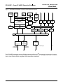
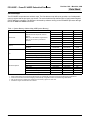
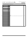
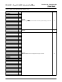
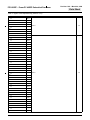
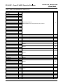
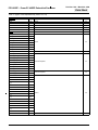
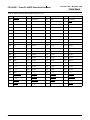
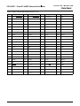
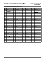
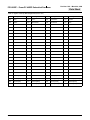
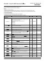
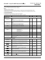
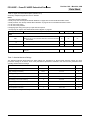
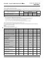
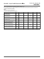
PPC405EP – PowerPC 405EP Embedded Processor
Revision 1.08 – March 24, 2008
Data Sheet
Table 6. Signal Functional Description (Sheet 1 of 6)
Secondary multiplexed signals are shown in brackets.
Notes:
1. Receiver input has hysteresis.
2. Must pull up. See “Pull-Up and Pull-Down Resistors” on page 29 for recommended termination values.
3. Must pull down. See “Pull-Up and Pull-Down Resistors” on page 29 for recommended termination values.
4. If not used, must pull up.
5. If not used, must pull down.
6. Strapping input during reset; pull up or pull down as required.
7. Pull-up may be required. See “External Bus Control Signals” on page 30.
Signal Name
Description
I/O
Type
PCI Address/Data Bus. Multiplexed address and data bus.
Note: The target device number is driven on PCIAD11:31 for PCI
Type 0 configuration transactions.
Connect the target IDSEL associated with device:
1 to PCIAD16
2 to PCIAD17
...
21 to PCIAD31.
I/O
5V tolerant
3.3V PCI
PCI bus command and byte enables.
I/O
5V tolerant
3.3V PCI
I
5V tolerant
3.3V PCI
Notes
PCI Interface
PCIAD00:31
PCIC3:0/BE3:0
PCIClk
PCIFrame
PCIFrame is driven by the current PCI bus master to indicate the
beginning and duration of a PCI access.
I/O
5V tolerant
3.3V PCI
PCIParity
PCI parity. Parity is even across PCIAD00:31 and PCIC3:0/BE3:0.
PCIParity is valid one cycle after either an address or data phase.
The PCI device that drove PCIAD00:31 is responsible for driving
PCIParity on the next PCI bus clock.
I/O
5V tolerant
3.3V PCI
PCIIRDY
PCIIRDY is driven by the current PCI bus master. Assertion of
PCIIRDY indicates that the PCI initiator is ready to transfer data.
I/O
5V tolerant
3.3V PCI
2
PCITRDY
The target of the current PCI transaction drives PCITRDY. Assertion
of PCITRDY indicates that the PCI target is ready to transfer data.
I/O
5V tolerant
3.3V PCI
2
PCIStop
The target of the current PCI transaction can assert PCIStop to
indicate to the requesting PCI master that it wants to end the current
transaction.
I/O
5V tolerant
3.3V PCI
2
PCIDevSel
PCIDevSel is driven by the target of the current PCI transaction. A
PCI target asserts PCIDevSel when it has decoded an address and
command encoding and claims the transaction.
I/O
5V tolerant
3.3V PCI
2
PCIIDSel
PCIIDSel is used during configuration cycles to select the PCI slave
interface for configuration.
I
5V tolerant
3.3V PCI
PCIINT
PCI interrupt. Open-drain output (two states; 0 or open circuit)
or
Peripheral write enable. Low when any of the four PerWBE0:3 write
byte enables are low.
O
5V tolerant
3.3V PCI
PCISErr
PCISErr is used for reporting address parity errors or catastrophic
failures detected by a PCI target.
I/O
5V tolerant
3.3V PCI
2
PCIPErr
PCIPErr is used for reporting data parity errors on PCI transactions.
PCIPErr is driven active by the device receiving PCIAD00:31,
PCIC3:0/BE3:0, and PCIParity, two PCI clocks following the data in
which bad parity is detected.
I/O
5V tolerant
3.3V PCI
2
PCI specific reset.
O
5V tolerant
3.3V PCI
Multipurpose signal, used as PCIReq0 when internal arbiter is used,
and as Gnt when external arbiter is used.
I
5V tolerant
3.3V PCI
PCIReset
PCIReq0/Gnt
AMCC
PCIClk is used as the asynchronous PCI clock when in asynch mode.
2
31