1
required to return the capacitor on pin 2 to the high level
voltage is duplicated and used to charge the capacitor connected to pin 3. Thus in one cycle of input the capacitor on
pin 3 gets charged twice with a charge of CV.
Input Hysteresis Amplifier
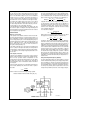
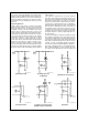
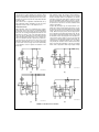
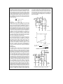
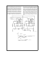
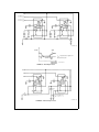
The equivalent schematic diagram is shown in Figure 2. Q1
through Q11 comprise the input hysteresis amplifier. Q1
through Q4 comprise an input differential amplifier which, by
virtue of PNP level shifting, enables the circuit to operate
with signals referenced to ground. Q7, Q8, D4, and D5 comprise an active load with positive feedback. This load behaves as a bi-stable flip-flop which may be set or reset depending upon the currents supplied from Q2 and Q3. Consider the situation where Q2 and Q3 are conducting equally,
i.e. the input differential voltage is zero. Assuming Q7 to be
conducting, it will be noted that the current from Q3 will be
drawn by Q7 and Q8 will be in the ‘‘OFF’’ state. This allows
the current from Q2 to drive Q7 in parallel with D4 and a
small resistor. D4 and Q7 are identical geometry devices, so
that the resistor causes Q7 to be biased at a higher level
than D4. Thus Q7 will be able to conduct more current than
Q3 provides. In order to reverse the state of Q7 and Q8, it
will be necessary to reduce the current from Q2 below that
provided by Q3 by an amount which is established by R1. It
can be shown that this requires a differential input to Q1 and
Q4, of approximately 15mV. Since the circuit is symmetrical,
the threshold voltage to reverse the state is 15 mV in the
other direction. Thus the input amplifier has built-in hysteresis at g 15 mV. This provides clean switching where noise
may be present on the input signal, and allows total rejection of noise below this amplitude where there is no input
signal.
Thus the total charge pumped into the capacitor on pin 3
per cycle is:
Q e 2 CV
(2)
Now, since V e VCC/2
then
Q e CVCC
(3)
A resistor connected between pin 3 and ground causes a
discharge of the capacitor on pin 3, where the total charge
drained per cycle of input signal is equal to:
V3 # T
R
where V3 e the average voltage on pin 3
T e period of input signal
R e resistor connected to pin 3
In equilibrium Q e Q1
V3 # T
i.e., CVCC e
R
Q1 e
RC
T
or
V3 e VCC # R # C # f
where f e input frequency
and
CV
I
(5)
(6)
Op Amp/Comparator
Again referring to Figure 2, the op amp/comparator includes
Q35 through Q45. A PNP input stage again provides input
common-mode voltages down to zero, and if pin 8 is connected to VCC and the output taken from pin 5, the circuit
behaves as a conventional, unity-gain-compensated operational amplifier. However, by allowing alternate connections
of Q45 the circuit may be used as a comparator in which
loads to either VCC or ground may be switched. Q45 is capable of sinking 50 mA. Input bias current is typically 50 nA,
and voltage gain is typically 200 V/mV. Unity gain slew rate
is 0.2 V/ms. When operated as a comparator Q45 emitter
will switch at the slew rate, or the collector of Q45 will
switch at that rate multiplied by the voltage gain of Q45,
which is user selectable.
Charge Pump
The charge pump is composed of Q12 through Q32. R4, R5,
and R6 provide reference voltages equal to 1/4 and 3/4 of
supply voltage to Q12 and Q13. When Q10 turns ‘‘ON’’ or
‘‘OFF,’’ the base voltage at Q16 changes by an amount
equal to the voltage across R5, that is 1/2 VCC. A capacitor
connected between Pin 2 and ground is either charged by
Q21 or discharged by Q22 until its voltage matches that on
the base of Q16. When the voltage on Q16 base goes low,
Q16 turns ‘‘ON,’’ which results in Q18 and Q26 turning on,
which causes the current, sourced by Q19 and Q20, to be
shunted to ground. Thus Q21 is unable to charge pin 2.
Meanwhile, Q27 and Q30 are turned off permitting the
200 mA sourced by Q28 and Q29 to enter the emitters of
Q31 and Q32 respectively. The current from Q31 is mirrored
by Q22 through Q24 resulting in a 200 mA discharge current
through pin 2. The external capacitor on pin 2 is thus discharged at a constant rate until it reaches the new base
voltage on Q16. The time taken for this discharge to occur is
given by:
te
V3 e VCC #
(4)
Active Zener Regulator
The optional active zener regulator is also shown in Figure
2. D8 provides the voltage reference in conjunction with
Q33. As the supply voltage rises, D8 conducts and the base
voltage on Q33 starts to rise. When Q33 has sufficient base
voltage to be turned ‘‘ON,’’ it in turn causes Q34 to conduct
current from the power source. This reduces the current
available for D8 and the negative feedback loop is thereby
completed. The reference voltage is therefore the zener
voltage on D8 plus the emitter base voltage of Q33. This
results in a low temperature coefficient voltage.
(1)
where
C e capacitor on pin 2
V e change in voltage on Q16 base
I e current in Q22
During this time, Q32 sources an identical current into pin 3.
A capacitor connected to pin 3 will thus be charged by the
same current for the same amount of time as pin 2. When
the base voltage on Q16 goes high, Q18 and Q26 are
turned off while Q27 and Q30 are turned ‘‘ON.’’ In these
conditions, Q21 and Q25 provide the currents to charge the
capacitors on pins 2 and 3 respectively. Thus the charge
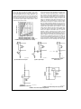
Input Levels and Protection
In 8-pin versions of the LM2907, LM2917, the non-inverting
input of the op amp/comparator is connected to the output
of the charge pump. Also, one input to the input hysteresis
amplifier is connected to ground. The other input (pin 1) is
then protected from transients by, first a 10kX series resis-
2