1
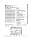
National Semiconductor
Application Note 260
January 1981
By combining an ‘‘inferior’’, 20 year old A/D conversion
technique with a microprocessor, a developmental A/D
converter achieves 1 part-per-million (20-bit) linearity. The
absolute accuracy of the converter is primarily limited by the
voltage reference available. The precision achieved by the
unlikely combination of technologies surpasses conventional approaches by more than an order of magnitude. The
approach used points the way towards a generation of
‘‘smart’’ converters, which would feature medium to high
resolution (12 bits and above) with high accuracy over extended temperature range. The conversion technique employed, while slow speed, suits transducer based measurement systems which require high resolution over widely
varying conditions of time and temperature. In addition, extensions of the basic converter have achieved 15-bit digitization of signal inputs of only 30 mV full-scale with no sacrifice in linearity or stability. This offers the prospect of an
‘‘instrumentation converter’’ which could interface directly
with low level analog signals.
One of the many A/D techniques utilized in the late 50’s and
early 60’s was the single-slope-integrating converter. One
form of this circuit compares a linear reference ramp to the
unknown voltage input (see About Integrating Converters
and Capacitors). When the ramp potential crosses the unknown input voltage a comparator changes state. The
length of time between the start of the ramp and the comparator changing state is proportional to the input voltage.
This length of time is measured digitally and presented as
the converter output. The inherent strengths of this type of
converter are simplicity and high linearity. Although singleslope-integrators were used in early A/Ds and voltmeters
their dependence on an integrating capacitor for stability
was considered an intolerable weakness. The advent of the
dual-slope converter (see About Integrating Converters and
Capacitors) solved the problem of integrating capacitor drift
with time and temperature by error cancellation techniques.
In a dual-slope converter the output represents the ratio of
the time required to integrate the unknown voltage for a
fixed time and then, using a reference voltage of opposing
polarity, measures the amount of time required to get back
to the original starting point (see About Integrating Converters and Capacitors). The technique eliminates capacitor
drift as an error term.
rent flow in the capacitor, including the magnitude, duration
and direction of current flow (see About Integrating Converters and Capacitors).
The nature of operation of dual-slope and related converters requires the instantaneous reversal of current in the integrating capacitor. This puts a substantial burden on the
dielectric absorption characteristics of the capacitor. Although dual-slope and related techniques go far to cancel
zero and full-scale drifts, residual non-linearity exists due to
the effects of dielectric absorption. In addition to non-linearity, dielectric absorption can also cause the converter to give
different outputs with a fixed input as the conversion rate is
varied over any significant range. Various compensation arrangements are employed to partially offset these effects in
present converters. What is really needed for high precision,
however, is a conversion scheme which inherently acts to
cancel the effects of dielectric absorption, while simultaneously correcting for zero and full-scale drifts.
Limitations of Dual-Slope Converters
The dual-slope converter, and variants on it, have been refined to a point where 16 and 17-bit resolution units are
available. A primary detriment to linearity in these converters is a parasitic effect in capacitors called dielectric absorption. Dielectric absorption can be conceptualized as a
slight hysteresis of response by the capacitor to charging
and discharging. It is influenced by the recent history of cur-
Overcoming Dual-Slope Limitations
Figure 1 diagrams a converter which meets the requirement
noted previously. In this arrangement a microprocessor is
used to sequentially switch zero, full-scale reference and EX
signals into one input of a comparator. The other comparator input is driven from the ramp output of an operational
amplifier integrator. With no convert command applied to
the microprocessor, the circuit is at quiescence. In this state
the microprocessor sends a continuous, regularly spaced
signal to the integrator reset switch. This results in a relatively fixed frequency, period and height ramp at the amplifier’s output. This relationship never changes, regardless of
the converter’s operating state. In addition, the time between ramps is lengthy, resulting in an effective and repeatable reset for the capacitor. When a convert command is
applied, the microprocessor switches the comparator input
to the zero position, waits for the next available ramp and
then measures the amount of time required for the ramp to
cross zero volts. This information is stored in memory. The
microprocessor then repeats this procedure for the fullscale reference and EX switch positions. With all this information, and the assumption that the integrator ramps are
highly linear, the absolute value of EX is determined by the
processor according to the following equation.
[CEX b CZERO]
c K mV
EX e
[CFULL-SCALE b CZERO]
where C e count obtained
and K e a constant, typically 107
After this equation is solved and the answer presented as
the converter’s output, the conversion is complete and the
microprocessor is ready to receive the next convert command.
A 20-Bit (1 ppm) Linear Slope-Integrating A/D Converter
A 20-Bit (1 ppm) Linear
Slope-Integrating A/D
Converter
AN-260
C1995 National Semiconductor Corporation
TL/H/5625
RRD-B30M115/Printed in U. S. A.
TL/H/5625 – 1
FIGURE 1
The converter arrangement shares many of the characteristics of a dual-slope type and also provides some significant
advantages. The key operating features are as follows:
1. It continuously corrects for zero and full-scale drift in all
components in the A/D circuit, regardless of changes in
time or temperature. The primary limitation on accuracy is
the stability of the full-scale reference. The zero signal is
derived through conventional high quality grounding technique. These features are similar to a dual-slope converter.
2. Because the integrating capacitor is always charged in a
continuous pattern and in the same direction, the dielectric absorption induced error will be relatively small, constant, and will appear as an offset term. This offset term
will be removed during the microprocessor’s calibration
cycle. This feature is unique to this converter and is the
key to high linearity.
3. The comparator always sees the ramp voltage approaching the trip point from the same direction and at the same
slew rate, regardless of operating conditions. This helps
maintain repeatability at the trip point in the face of noise
and gain-bandwidth limitations in the comparator.
3. Unlike a dual-slope, this converter has no inherent noise
rejection capability. The EX input signal is directly coupled to the comparator input with no filtering. This is a
decided disadvantage because most ‘‘real world’’ signals
require some smoothing. If a filter was placed at the input
substantial time lag due to settling requirements would
occur. This is unacceptable because the converter relies
on short time intervals between multiplexer states to effectively cancel drift. The solution is to use the microprocessor to filter the signal digitally, using averaging techniques.
Filling Out the Blocks
The detailed schematic diagram of the prototype 20-bit linear A/D conveter is shown in Figure 2 . For clarity, the details of the INS8070 microprocessor and its associated logic
are shown in block from. Note that the entire analog section
of the converter is fully floating from the digital section to
eliminate noise due to digital current spiking and clock
noise. The analog and digital circuits communicate via optoisolators. The full-scale reference for the converter is provided by the LM199A-20-LM108A combination. This circuit,
using the components specified, will typically deliver 0.25
ppm/§ C performance with drift of several ppm per year. The
accuracy to which this reference can be maintained is the
primary limitation on absolute accuracy in this converter.
The output of this reference is fed to an FET-switched multiplexer which also receives the EX and zero signals. Because all these sources are at low impedance, and only one
is switched on at a time, the leakage and ON resistances do
not contribute significant error. The A4 combination provides a low bias current unity gain follower with greater than
1,000,00:1 (120 dB) of CMRR, preserving converter linearity. Drifts in this follower are not significant because they will
be cancelled out by the microprocessor’s calibration cycle.
The microprocessor’s digital commands to the FET
switches are received by the 4N28 opto-isolators. The
LM148 quad op-amp (A5) is used to generate the voltage
swing necessary to control the FET switches. The discrete
components at each amplifier output are used to generate
one-way time delays to give the FET switches break-beforemake action. This prevents cross talk between the zero, fullscale reference and EX sources.
2
TL/H/5625 – 2
FIGURE 2
The requirement for a comparator with 1 ppm (1 LSB at 20
bits e 1 ppm) of trip point noise cannot be met by any standard device. At 10V full-scale this is only a 10 mV LSB. The
50 ms-10V ramp’s relatively slow slew rate means that the
gain-bandwidth and noise characteristics of a standard differential input comparator will cause considerable uncertainty at the trip point. Also, as the common-mode voltage at which the ramp vs EX crossing occurs changes,
the trip point of the comparator will shift, introducing
overall non-linearity.
Another FET is used to reset the integrator and is biased by
a ‘‘brute-force’’ level shifting-edge speed-up network
formed by the 2N2222-2N2369 pair. A 4N28 opto-isolator
biases this network when it receives the reset signal
from the INS8070 processor. A1, an LF356, has its ‘‘ a ’’
input biased at about negative 1V, ensuring that
the ramp will start far enough below ground to determine a
true zero signal.
3
These problems are addressed by the A2-A3 configuration,
which forms a high precision comparator. A4’s negative output is resistively summed with the positive output of the A1
ramp at A2. A2 normally operates at a low gain due to the
diode bounding in its feedback loop. When the currents produced by the ramp potential and A4’s output very nearly
balance the potential at A2’s summing junction will go low
enough so that A2 comes out of bound and operates at a
gain determined by the 499k feedback resistor (about 100).
A2 remains in this high-gain state as long as the ramp and
A4 output caused currents are nearly equal. As the ramp
continues in its positive going direction the current into A2’s
summing junction will go to zero and then move positive
until the A2 output bounds negative. The output of A2 drives
A3, an LM311 comparator which is set up as a zero crossing
detector. The components in the positive feedback path at
A3 insure a sharp transition. Figure 3 shows the waveforms
of operation. The ramp (a) is shown in highly expanded
form. The A2 output (b) can be seen to come cleanly out of
diode-bound just before the ramp balances A4’s output and
then return to bound after the crossing occurs. Waveform
(c) is A3’s output. The A2 pre-amplifier makes the A3 comparator’s job much easier in a number of ways. It amplifies
the voltage difference of the two signals to be compared by
a factor of 100. This knocks down the effect of A3’s input
uncertainties. It also produces an apparent 100 fold increase in the ramp slew rate at the trip point. This means A3
spends that much less time with its inputs nearly balanced
in an uncertain and noise sensitive condition. Finally, A2
presents the difference signal as a single ended zero crossing signal. This eliminates errors due to changing commonmode voltages that a differential comparator’s input would
face. Such errors would manifest themselves as overall
converter non-linearity.
Converter Performance and Testing
Figure 4 shows the convert at work. A complete conversion
cycle is captured in the photograph. Waveform (a) is the
integrator reset out of the INS8070. (b) is the ramp at A1’s
output. Waveform (c) is the multiplexer output at A4, showing the zero, full-scale reference and EX states. For each
state ample time is allowed before the ramp begins. The
width output is shown in waveform (d).
TL/H/5625 – 4
FIGURE 4
The converter was tested with the arrangement shown in
Figure 5 . The Kelvin-Varley voltage divider, a primary standard type, has a guaranteed linearity of within 1 ppm. The
LM11 op amp provides a low bias current, low drift follower
to unload the Kelvin divider’s output impedance. Because
the LM11 gives greater than 120 dB common-mode rejection, its voltage output should track the linearity of the Kelvin
divider. To test this the LM11 was adjusted for offset null
and a battery-powered mV meter connected between its inputs. 20-bit linear (1 ppm) transfer characteristics were verified by running the Kelvin divider through its range and noting less than 10 mV (1 LSB at 10V full-scale) shift under all
conditions. Then, the converter reference was used to drive
the Kelvin divider input and the LM11 output to the EX input
of the A/D converter.
TL/H/5625–3
FIGURE 3
The output of the A3 comparator feeds a 2N2369 transistor,
which functions as a level shifter-gate. This transistor gates
out that portion of the width output pulse which would be
due to the length of the integrator reset pulse. The 2N2369,
a low storage capacitance device, provides high speed,
even in the relatively slow common emitter configuration.
The HP-2602 high speed opto-coupler transmits the width
information to the digital circuitry.
TL/H/5625 – 5
FIGURE 5
4
bridge output for a given bridge drive level. In this manner,
even if the bridge drive varies, the gain of the system remains calibrated by ratiometric error cancellation. The zero
signal is derived by shorting both amplifier inputs to the
common-mode voltage at the bridge output. This system
has been built and has maintained 15-bit accuracy over a
75§ F temperature range.
Prospective constructors of this converter are advised that
construction technique is extremely critical. In order for the
converter to operate properly, the greatest care must be
taken in grounding, guarding and shielding techniques. Useful sources of information are listed in the References
A typical output on the Hewlett-Packard 2644A CRT terminal display is shown in Figure 6 . For each convert command
to the INS8070 the number of counts of zero, full-scale reference and EX are shown along with the final computed
answer. Note that the final count is computed to one part in
ten million and the last digit is insignificant. Note also that
the 4 final counts are all within g 1 ppm . . . despite the fact
that they were individually spaced almost 1 hour apart in a
varying thermal environment. Linearity of the converter over
a 10V range was verified at 10 points by varying the MSB of
the Kelvin divider. Although the prototype converter takes
300 ms to complete a cycle, faster speed is attainable by
increasing the 20 MHz clock rate. Perhaps more practically,
higher conversion speeds at lower resolutions are easily attainable by simply shortening the ramp time. The converter
output word length and conversion time may be varied over
a wide dynamic range by juggling clock speed and ramp
time.
References
1. ‘‘Grounding and Shielding Techniques in Instrumentation’’, R. Morrison; Wiley Interscience.
2. ‘‘Designing Sensitive Circuits? Don’t Take Grounds for
Granted!’’, A. P. Brokaw; EDN, October 5, 1975.
3. ‘‘Input Connection Practices for Differential Amplifiers’’,
J. H. Hueckel; Neff Inst. Corp.
4. ‘‘Prevent Low Level Amplifier Problems’’, J. Williams;
Electronic Design, February 15, 1975.
5. ‘‘Signal Conditioning’’, Gould Inc., Brush Insts. Div.,
Cleveland, Ohio.
6. ‘‘On Computing Errors of an Integrator’’, T. Miura, et. al;
Proc. 2nd ALCA Conf. Strasbourg, France. 1958. Presses Academiques Europeennes, Brussels.
7. ‘‘Comparator I.C. Forms 10-Bit A/D Converter’’, J. Williams: Electronics, April 17, 1975.
8. ‘‘Low Cost, Linear A/D Conversion Uses Single-Slope
Techniques’’, J. Williams: EDN, August 5, 1978.
9. Component Research Corp.ÐCatalog JB.
10. ‘‘The Secret Life of Capacitors’’, ECD Corp., Cambridge,
Massachusetts.
11. ‘‘An Analysis of Errors in Single Slope Integrators’’, R. A.
Eckhardt; S. B. Thesis, M.I.T., 1974.
12. ‘‘Characterization, Measurement and Compensation of
Errors in Capacitors . . . a compendium of study, hacks,
some good stuff and a few pearls’’, J. Williams; Massachusetts Institute of Technology, Cambridge, Massachusetts, 1975.
13. ‘‘Operating and Service Manual Ð HP3440 D.V.M.’’;
Hewlett-Packard Co., 1961.
TL/H/5625 – 6
FIGURE 6
Although demonstrating a 20-bit converter is useful, there
are other applications which do not require this degree of
precision. The basic technique is readily adaptable to the
practical solution of common transducer and other low-level
interface problems. Figure 7 shows the block diagram of the
converter used to generate a 15-bit output directly from a 30
mV full-scale input. In this application the converter input is
a differential input amplifier with a nominal gain of 300. Note
that the amplifier’s offset and gain drift will be cancelled by
the microprocessor’s calibration loop. The EX signal is the
output of the transducer bridge. The full-scale reference signal is derived by measuring across the middle resistor of a
string which has the same voltage across it as the nominal
FIGURE 7
5
TL/H/5625 – 7
Both of these converters are dependent to varying degrees
on capacitor characteristics. The single-slope type requires
stability in the capacitor over time and temperature while the
dual-slope gets around this limitation. The effects of a phenomenon in capacitors called dielectric absorption, however, have direct impact on dual-slope performance. Dielectric
absorption is due to the capacitor dielectric’s unwillingness
to accept or give up charge instantaneously. It is commonly
and simply modeled as a parasitic series RC (Figure C )
across the terminals of the main capacitor.
If a charged capacitor is discharged, even through a dead
short, some degree of time will be required to remove all of
the charge in the parasitic capacitance due to the parasitic
series resistance. Conversely, some amount of charge will
be absorbed by the parasitic capacitor after a charging of
the main capacitor has ceased unless the charge source is
maintained for many parasitic RC time constants. Various
dielectrics offer differing performance with respect to dielectric absorption. Teflon, polystyrene and polypropylene are
quite good, while paper, mylar and glass are relatively poor.
Electrolytics are by far the worst offenders. Anyone who has
received a shock after discharging a high voltage electrolytic in a television set has experienced the effect of dielectric
absorption.
About Integrating Converters and Capacitors
The simplest form of integrating converter is the singleslope type (Figure A ). In the single-slope unit shown, a linear
reference ramp is compared against the unknown input, EX.
When the switch across the integrator capacitor is opened,
the ramp begins. The time interval between the opening of
the integrator reset switch and the comparator changing
state (when ERAMP e EX) is directly proportional to the value of EX. This converter requires that the integrating capacitor and the clock used to measure the time interval be stable over time and temperature . . . a significant drawback
under normal circumstances.
The dual-slope integrator (Figure B ) overcomes these problems by effectively normalizing the capacitor value and
clock rate each time a conversion is made. It does this by
integrating the EX input for a pre-determined time. Then, the
voltage reference is switched to the integrator input which
proceeds to integrate in a negative going direction from the
EX slope. The length of time the reference slope requires to
get back to zero is proportionate to the EX signal value.
These slopes are both established with the same integrating
capacitor and measured with the same clock, so both parameters need only be stable over one conversion cycle.
TL/H/5625 – 9
FIGURE A
TL/H/5625 – 8
FIGURE C
FIGURE B
6
7
A 20-Bit (1 ppm) Linear Slope-Integrating A/D Converter
LIFE SUPPORT POLICY
NATIONAL’S PRODUCTS ARE NOT AUTHORIZED FOR USE AS CRITICAL COMPONENTS IN LIFE SUPPORT
DEVICES OR SYSTEMS WITHOUT THE EXPRESS WRITTEN APPROVAL OF THE PRESIDENT OF NATIONAL
SEMICONDUCTOR CORPORATION. As used herein:
AN-260
1. Life support devices or systems are devices or
systems which, (a) are intended for surgical implant
into the body, or (b) support or sustain life, and whose
failure to perform, when properly used in accordance
with instructions for use provided in the labeling, can
be reasonably expected to result in a significant injury
to the user.
National Semiconductor
Corporation
1111 West Bardin Road
Arlington, TX 76017
Tel: 1(800) 272-9959
Fax: 1(800) 737-7018
2. A critical component is any component of a life
support device or system whose failure to perform can
be reasonably expected to cause the failure of the life
support device or system, or to affect its safety or
effectiveness.
National Semiconductor
Europe
Fax: (a49) 0-180-530 85 86
Email: cnjwge @ tevm2.nsc.com
Deutsch Tel: (a49) 0-180-530 85 85
English Tel: (a49) 0-180-532 78 32
Fran3ais Tel: (a49) 0-180-532 93 58
Italiano Tel: (a49) 0-180-534 16 80
National Semiconductor
Hong Kong Ltd.
13th Floor, Straight Block,
Ocean Centre, 5 Canton Rd.
Tsimshatsui, Kowloon
Hong Kong
Tel: (852) 2737-1600
Fax: (852) 2736-9960
National Semiconductor
Japan Ltd.
Tel: 81-043-299-2309
Fax: 81-043-299-2408
National does not assume any responsibility for use of any circuitry described, no circuit patent licenses are implied and National reserves the right at any time without notice to change said circuitry and specifications.