1
q SERVICE MANUAL
CODE : 00ZERA520USME
ELECTRONIC
CASH REGISTER
ER-A520
MODEL ER-A530
ER-A520
(U, A version)
ER-A530
CONTENTS
CHAPTER 1. SPECIFICATIONS . . . . . . . . . . . . . . . . . . . . . . . . . . . . 1
CHAPTER 2. OPTIONS . . . . . . . . . . . . . . . . . . . . . . . . . . . . . . . . . . . 5
CHAPTER 3. MASTER RESET AND PROGRAM RESET. . . . . . . . . 6
CHAPTER 4. HARDWARE DESCRIPTION . . . . . . . . . . . . . . . . . . . . 7
CHAPTER 5. DIAGNOSTIC PROGRAM . . . . . . . . . . . . . . . . . . . . . 14
CHAPTER 6. IPL FROM EP-ROM . . . . . . . . . . . . . . . . . . . . . . . . . . 19
CHAPTER 7. CIRCUIT DIAGRAM AND PWB LAYOUT . . . . . . . . . 20
PARTS GUIDE
Parts marked with "!" are important for maintaining the safety of the set. Be sure to replace these parts with specified
ones for maintaining the safety and performance of the set.
SHARP CORPORATION
This document has been published to be used
for after sales service only.
The contents are subject to change without notice.
CHAPTER 1. SPECIFICATIONS
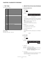
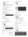
1. APPEARANCE
3-2. KEY LAYOUT
ER-A520
ER-A520
Front view
Printer
cover lock
(left side)
Customer display (Pop-up type)
Printer cover
Receipt paper
Journal window
■ STANDARD KEY LAYOUT
Rear view
Operator
display
SLIP
PLU/UPC
RCPT PBLU
@
FOR
CL
5
10
15
20
Mode
switch
Printer cover
Receipt paper
Journal window
FS AUTO
TEND
2
RA
FINAL
7
8
9
4
9
14
19
NS
CH1
%1
TAX
4
5
6
3
8
13
18
CHK
CH2
TAX
SHIFT
1
2
3
2
7
12
17
MDSE
SBTL
SBTL
00
1
6
11
16
CA/AT
0
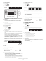
■ TEXT PRESET KEY LAYOUT
`
Customer display
(Pop-up type)
(Back
Space)
NUM
Rear cover
V
^
Printer
cover lock
(left side)
CL
@/FOR
A
~
7
8
9
'
`
4
5
6
:
1
2
3
+
00
<
O
Rear view
Operator
display
-2
0
B
C
D
E
F
*
;
G
H
>
I
J
#
@
,
=
Pt
K
L
M
N
O
$
/
.
P
Q
R
Rear cover
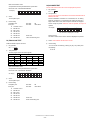
2. RATING
2 RECEIPT
Receipt paper feed key
2 JOURNAL
Journal paper feed key
[0]~[9], [00]
Numeric keys
[•]
Decimal point key
CL
Clear key
@/FOR
Multiplication key
RFND
Refund key
VOID
Void key
AMT
Amount entry key
Model
ER-A520/530
CASH#
Cashier code entry key
Weight
31.7lbs (14.4kg)
PLU/UPC
PLU/UPC key
Dimensions
421 (W) x 427 (D) x 297 (H) mm
16.6 (W) x 16.8 (D) x 11.7 (H) inch
INQ
PLU/UPC inquiry key
Power source
120V m10%, AC 60Hz
PRICE CHANGE
UPC price change key
Stand-by 11W, Operating 47W (max.)
-
Discount 1 key
Power consumption
%1, %2
Percent 1 and 2 keys
Working temperature
0°C~40°C (32°F to 104°F)
NC
New check key
PBLU
Previous balance key
FINAL
Final key
NS
No-sale key
TAX SHIFT
TAX 1 shift key
3-1. KEYBOARD LAYOUT
TAX
Manual tax key
ER-A520
MDSE SBTL
Merchandise subtotal key
1 ~ 20
Department keys
3. KEYBOARD
Normal keyboard
Key stroke
3.5 m 0.5 mm
Key pitch
19 (W) x 19 (H) mm
ER-A530
Type
Flat key
Key stroke
0.8 m 0.2 mm
Key pitch
18 (W) x 15 (H) mm
(
!
U
V
W
&
)
?
X
Y
Z
S
£
T
■Standard Key names and Descriptions
Mode
switch
Type
%
Note: All keys except the receipt paper feed and journal paper feed
keys can be re-positioned.
Keyboard
Drawer
Drawer lock
AUTO
1
PO
ER-A530
Front view
AMT INQ SHIFT
CONV
RFND VOID #/TM
Drawer
Drawer lock
FS
CASH#
%2
Keyboard
PRICE
CHANGE
NC
ER-A520U/ER-A530U
AUTO1~AUTO2
Automatic sequencing 1 and 2 keys
RA
Received-on-account 1 key
PO
Paid-out 1 key
FS SHIFT
Food stamp shift key
FS TEND
Food stamp tender key
CH1, CH2
Charge 1and 2 keys
CONV
Currency conversion key
CHK
Check 1 key
SBTL
Subtotal key
CA/AT
Cash/Amount tendered key
RCPT
Receipt print key
SPECIFICATIONS
–1–
SLIP
Slip printer key
ER-A530
#/TM
Non-add code/Date & time display key
■ STANDARD KEY LAYOUT
RECEIPT
Note: The following function keys can optionally be incorporated in place
of those shown in the figure of the standard keyboard layout. For
details, please consult your authorized SHARP dealer.
JOURNAL
91
92
93
94
95
97
96
98
99
79
80
81
82
83
84
85
86
87
88
89
90
67
68
69
70
71
72
73
74
75
76
77
78
65
SERV
#
66
56
57
58
59
60
61
62
63
64
L1
L2
RCPT
%
100
VOID
INQ
RFND
PLU/
SUB
@
45
■ Optional Key Names and Descriptions
46
47
48
49
50
51
52
53
54
55
FOR
8
CL
9
38
39
40
41
42
43
44
26
27
28
29
30
31
32
33
4
5
6
FINAL
CH3
3
MDSE
SBTL
CHK
SBTL
CA/AT
%3 ~ %5
Percent 3 thru 5 keys
16
17
18
19
20
21
22
1
2
- 2 ~ -5
Discount 2 thru 5 keys
1
2
3
4
5
6
7
8
9
10
11
0
00 000
CH3 ~ CH9
Charge 3 thru 9 keys
CA2 ~ CA5
Cash 2 thru 5 keys
CONV2 ~ CONV4
Currency conversion 2 thru 4 keys
RA2
■ TEXT PRESET KEY LAYOUT
Ñ
RECEIPT JOURNAL
¿
{
}
>
[
BACK
SPEACE
]
”
”
?
<
!
@
#
$
%
^
&
(
)
=
Received-on-account 2 key
1
2
3
4
5
6
7
8
9
0
-
PO2
Paid-out 2 key
Q
W
E
R
T
Y
U
I
O
P
/
AUTO3 ~ AUTO10
Automatic sequencing 3 thru 10 keys
A
S
D
F
G
H
J
K
L
:
7
8
9
SRVC
Service key
Z
X
C
V
B
N
M
,
;
.
_
4
5
6
1
2 3
00 000
Transfer out key
TRANS IN
Transfer in key
CA TIP
Cash tip key
CH TIP
Charge tip key
TIP PAID
Tip paid key
EAT IN1~EAT IN3
Eat in 1 thru 3 keys
TAX2 SHIFT~TAX4 SHIFT
Tax 2 thru 4 shift keys
DEPO
Deposit key
DEPORFND
Deposit refund key
LEVEL#
PLU level shift number key
RP SEND
Remote printer send key
GRT EXEMPT
Gratuity exempt key
OPEN TARE
Tare entry key
REPEAT
Repeat entry key
GASSBTL
Gasoline sales subtotal key
P-SHIFT#
Price shift number key
■Standard Key Names and Descriptions
P1~P6
Price level shift 1 thru 6 keys
PRINT
Validation print key
CVCNT
Cover count entry key
NO DEL
No delete key
BS
Bill separation key
BT
Bill totalize/Bill transfer key (CHECK-ADD)
BIRTH
Birthday entry key
RFND SALES
Refund sales key
C CANCEL
Condiment cancel key
EDIT TIP
Edit tip key
GLU RECALL
Table# recall key
000
Numeric key
CA/AT
• Please note that the Price lookup/subdepartment/UPC key
([PLU/SUB]) and the previous balance key ([PBLU]) are shown
as [PLU/UPC] and [PBLU] respectively in this manual.
PLU/UPC PBAL
Scale entry key
Condiment next key
SBTL
Note: • All keys except the receipt paper feed and journal paper feed
keys may be re-positioned.
If you want to change the keyboard layout, please consult your
dealer.
PLU level shift 1 thru 5 keys
Waste mode key
CL
FOR
0
L1~L5
C NEXT
+
@
(SHIFT) (DC)
SCALE
WASTE
CH2
37
15
Check 2 through 5 keys
CH1
SRVC
25
14
TRANS OUT
CONV
36
13
CHK2~CHK5
NC
PBAL
24
12
Tray subtotal key
AUTO
3
35
Dept. number key
Return key
RP
SEND
34
DEPT#
RETURN
AUTO
1
AUTO
2
7
23
TRAY SBTL
L3
2 RECEIPT
2 JOURNAL
[0] ~ [9], [00], [000]
[•]
CL
@/FOR
RCPT
RFND
VOID
PLU/SUB
[ 1] ~ [100]
L1~L3
NC
SRVC
FINAL
PBAL
%
INQ
SERV#
AUTO1 ~ AUTO3
CONV
CH1 ~ CH3
CHK
MDSE SBTL
SBTL
CA/AT
RP SEND
Note: The department and direct PLU keys may be expanded. If you
require expansion of the department or direct PLU keys, please
contact your dealer.
Receipt paper feed key
Journal paper feed key
Numeric keys
Decimal point key
Clear key
Multiplication key
Receipt print key
Refund key
Void key
Price lookup/subdepartment/UPC key
Direct price lookup keys
PLU level shift 1 thru 3 keys
New check key
Service key
Final key
Previous balance key
Discount 1 key
Percent 1 key
PLU/UPC inquiry key
Server code entry key
Automatic sequencing 1 thru 3 keys
Currency conversion key
Charge 1 thru 3 keys
Check 1 key
Merchandise subtotal key
Subtotal key
Cash/amount tendered key
Remote printer send key
Note: The following function keys can optionally be added in place of
those shown in the figure of the standard keyboard layout. For
details, please consult your authorized SHARP dealer.
ER-A520U/ER-A530U
SPECIFICATIONS
–2–
4. MODE SWITCH
■ Optional Keys and Descriptions
DEPT#
Dept. number key
%2 ~ %5
Percent 2 thru 5 keys
- 2 ~ -5
Discount 2 thru 5 keys
CH4 ~ CH9
Charge 4 thru 9 keys
4-1. MODE SWITCH AND MODE KEYS
Operative range
CA2 ~ CA5
Cash 2 thru 5 keys
MA
CONV2 ~ CONV4
Currency conversion 2 thru 4 keys
SM
RA1, RA2
Received-on-account 1 and 2 keys
PO1, PO2
Paid-out 1 and 2 keys
AUTO4 ~ AUTO10
Automatic sequencing4 thru 10 keys
CHK2 ~ CHK5
Check 2 through 5 keys
OP X / Z
TRANS OUT
Transfer out key
OFF
TRANS IN
Transfer in key
PGM1
CA TIP
Cash tip key
CH TIP
Charge tip key
PGM2
(SRV)
TIP PAID
Tip paid key
REG
EAT IN1 ~ EAT IN3 Eat in 1 thru 3 keys
TAX1 SHIFT ~
TAX4 SHIFT
TAX
Manual tax key
TRAY SBTL
Tray subtotal key
RETURN
Return key
GAS SBTL
Gasoline sales subtotal key
No-sale key
SCALE
Scale entry key
PLU level shift number key
PLU level shift 4 and 5 keys
P-SHIFT#
Price shift number key
P1 ~ P6
Price level shift 1 thru 6 keys
PRINT
Validation print key
CV CNT
Cover count entry key
SLIP
Slip printer key
BS
Bill separation key
OP
Non-add code/Date & time display key
NS
L4, L5
• Submanager key (SM)
• Operator key (OP)
#/TM
LEVEL#
(SRV')
SM
Deposit refund key
X2/Z2
MA
Deposit key
DEPO RFND
X1 /Z1
• Manager key (MA)
Tax 1 thru 4 shift keys
DEPO
MGR
The mode switch has these settings:
OFF:
This mode locks all register operations.
No changes may occur to register data.
BT
Bill totalize/Bill transfer key (CHECK-ADD)
NO DEL
No delete key
GRT EXEMPT
Gratuity exempt key
OP X/Z: This setting allows cashiers to take an X or Z reports for their
sales information. This mode can also be used for displaying
the date/time and printing the employee's arrival/departure
times. This mode can be also used to toggle receipt state "ON"
and "OFF" by pressing the [RCPT] key. (To utilize this function, the register must be programmed for "OP X/Z mode available" in the PGM2 mode.)
OPEN TARE
Tare entry key
REG:
REPEAT
Repeat entry key
AMT
Amount entry key
PRICE CHANGE
UPC price change key
BIRTH
Birthday entry key
RFND SALES
For entering sales
PGM1: To program those items that need to be changed often: e.g.,
unit prices of departments or PLUs, and percentages.
Refund sales key
PGM2: To program all PGM1 programs and those items that do not
require frequent changes: e.g., date, time, or a variety of register functions.
WASTE
Waste mode key
MGR:
C NEXT
Condiment next key
C CANCEL
Condiment cancel key
For manager’s and submanager’s entries
The manager can use this mode to make entries that are not
permitted to be made by cashiers in the REG mode.
– for example, after-transaction voiding and override entries.
X1/Z1:
To take the X/Z reports for various daily totals.
X2/Z2:
To take the X/Z reports for various periodic (weekly or monthly)
consolidation of totals.
EDIT TIP
Edit tip key
GLU RECALL
Table# recall key
FS SHIFT
Food stamp shift key
FS TEND
Food stamp tender key
Note: Department and direct PLU keys can be expanded. If you require
expansion of the department or direct PLU keys, please contact
your authorized SHARP dealer.
ER-A520U/ER-A530U
SPECIFICATIONS
–3–
5. DISPLAY
6. PRINTER
1) PRINTER (PR-58HM)
5-1. OPERATOR DISPLAY
Display device:
LCD
Number of lines:
2 lines
Item
Number of positions: 16 positions
Color of display:
Description
No. of station
2: Receipt and Journal
Validation
No
Printing system
Line thermal
No. of dot
Receipt:
Yellow / Green
Character font:
5 x 7 dot
Character size:
4.84 (W) x 8.06 (H) mm
Dot pitch
Layout:
360 dots
Journal
360 dots
Horizontal:
0.125mm
Vertical:
0.125mm
Font
10 dots (W) x 24 dots (H)
Printing capacity
Receipt:
Max. 30 characters
Journal:
Max. 30 characters
1.25 mm (W) x 3.0 mm (H): At 10 x 24 dots
Character size
Print pitch
Column distance: 1.5 mm
Row distance:
Paper feed speed
5-2. CUSTOMER DISPLAY
3.75 mm
Approximate 65 mm/s
Reliability
Mechanism:
Paper end sensor
Yes (Receipt and Journal)
Cutter
Manual
Paper near end sensor
No
MCBF 5million lines
Printing area
Display device:
LED
Number of lines:
1 line
106(848dots)
(7.0)
(5.5)
360dots
(45)
Number of positions: 7 positions
Yellow / Green
Style:
Pop up type
Character form:
7 segment + decimal point
Character size:
14.2mm (H) x 7.9mm (W)
0.125
(5.5)
57.5 ± 0.5
Printing format
12 x 24
font
1.5 (12dots)
UNIT: mm
1.5 (12dots)
0.125
3.75 (30dots)
3.75 (30dots)
0.125
Layout:
5.0
(7.0)
3.0 (24dots)
Color of display:
UNIT: mm
2) PAPER
Item
ER-A520U/ER-A530U
Heat-quality paper
Roll dimension
57.5 m 0.5 mm in width
Thickness
0.06 mm to 0.08 mm
SPECIFICATIONS
–4–
Description
Name
7. DRAWER
7-3. LOCK (LOCK KEY: LKGIM7331BHZZ)
[OUTLINE]
• Location of the lock: Front
• Standard equipment: Yes
• Method of locking and unlocking:
• Max. number of additional drawers: 1
To lock, insert the drawer lock key into the lock and turn
it 90 degrees counter clockwise.
To unlock, insert the drawer lock key and turn it 90
degrees clockwise.
• The drawer consists of:
1) Drawer box (outer case) and drawer
2) Money case
SK1-1
Model name of the drawer
box
SK1-1
7-1. DRAWER BOX AND DRAWER
SK423
Size
420 (W) x 427 (D) x 112 (H) mm
color
Gray 368
Material
Metal
Bell
–
Release lever
Standard equipment: located on the
bottom
Drawer open sensor
YES
Lo
[SPECIFICATION]
ck
unlo
Key No:
3) Lock (attached to the drawer)
7-2. MONEY CASE
For U version
Separation from the drawer
Separation of the coin compartments from the money case
Bill separator
Number of compartments
For A version
Allowed
Allowed
Disallowed
Allowed
No
No
5B/5C
5B/6C
For U version
For A version
5B/5C
5B/6C
CHAPTER 2. OPTIONS
1.OPTIONS
NO
CLASSIFICATION
COMPONENT NAME
MODEL NAME
1
Drawer
Remote drawer
ER-03DW
2
Key kit
1 x 1 key top kit (30)
ER-11KT7
1 x 2 key top kit (30)
ER-12KT7
2 x 2 key top kit (10)
ER-22KT7
REMARK
ER-04DW
1 x 1 dummy key kit (30)
ER-11DK7G
5 x 1 dummy key kit (10)
ER-51DK7G
3
Display
Customer Pole Display
4
Memory
RAM board
UP-P16DP
UP-S02MB
ER-A520U/ER-A530U
–5–
OPTIONS
ER-A520 only
ck
CHAPTER 3. MASTER RESET AND PROGRAM RESET
3. PROGRAM RESET
The SRV key is used for performing entries in the SRV mode.
A MASTER RESET clears the entire memory and resumes initial values.
Please use either “Procedure A”, “Procedure B” or “Procedure C”
A PROGRAM RESET resumes the initial program without clearing the
memory.
Procedure A: 1) Set the mode switch to the (SRV’) position.
2) Plug in the AC power cord to the wall outlet.
There are 2 kinds of MASTER RESET operations.
3) Without pressing the JOURNAL FEED key, turn the
mode switch to (SRV) position from the (SRV’) position.
MASTER RESET 1: Normal MASTER RESET
Clears the entire memory and resumes initial
values.
Procedure B: 1) Unplug the AC power cord from the wall outlet.
MASTER RESET 2: It enables the layout of fixed keys in addition to
MASTER RESET 1.
2) Set the mode switch to the (SRV) position.
3) Without pressing the JOURNAL FEED key, plug in
the AC power cord from the wall outlet.
Fixed keys: [0] [1] [2] [3] [4] [5] [6] [7] [8] [9]
[00] [000] [.] [CL] [@/FOR] [SBTL]
[CA/AT]
Procedure C: 1) Unplug the AC power cord from the wall outlet.
2) Set the mode switch to the PGM2 position.
3) While holding down the JOURNAL FEED key & the
RECEIPT FEED key, plug in the AC power cord to the
wall outlet.
1. MASTER RESET 1
Please use “Procedure A” or “Procedure B”
* “Procedure C” can be executed when SRV#916-B is +4: PROGRAM
RESET in PGM2 = ENABLE.
Procedure A: 1) Set the mode switch to the (SRV’) position.
Note: Procedure B and C cannot reset the hardware.
Procedure A must be used to reset the hardware.
2) Plug in the AC power cord to the wall outlet.
3) While holding down the JOURNAL FEED key, turn
the mode switch to (SRV) position from the (SRV’)
position.
Procedure B: 1) Unplug the AC power cord from the wall outlet.
2) Set the mode switch to the (SRV) position.
3) While holding down the JOURNAL FEED key, plug in
the AC power cord to the wall outlet.
Note: Procedure B cannot reset the hardware.
Procedure A must be used to reset the hardware.
2. MASTER RESET 2
Please use “Procedure A” or “Procedure B”
Procedure A: 1) Set the mode switch to the (SRV’) position.
2) Plug in the AC power cord to the wall outlet.
3) While holding down the JOURNAL FEED & the
RECEIPT FEED keys, turn the mode switch to the
(SRV) position from the (SRV’) position.
4) Program the [0] [1] [2] [3] [4] [5] [6] [7] [8] [9] [00] [000]
[.] [CL] [@/FOR] [SBTL] [CA/AT] keys by depressing
the keys in this order.
Note: If the [000] key is not required, press the same
key in the next step, and the [000] key will be
inhibited.
Procedure B: 1) Unplug the AC power cord from the wall outlet.
2) Set the mode switch to the (SRV) position.
3) While holding down the JOURNAL FEED & the
RECEIPT FEED key, plug in the AC power cord to the
wall outlet.
4) Repeat the same sequence as in “Procedure A”
Note: Procedure B cannot reset the hardware.
Procedure A must be used to reset the hardware.
ER-A520U/ER-A530U
MASTER RESET AND PROGRAM RESET
–6–
CHAPTER 4. HARDWARE DESCRIPTION
1. BLOCK DIAGRAM
2. MEMORY MAP
ER-A520 and ER-A530
2-1. ADDRESS MAP
DRAWER1
000000h
000400h
Microprocessor mode : MODE0
IPLION0# "L" IPLON0# "H"
SFR AREA
INTERNAL RAM AREA(10KB)
INTERNAL RESERVE AREA
DRAWER2
㪧㪦㪮㪜㪩㩷㪪㪦㪬㪚㪜
000800h
RAM
OPT RAM
NOT USED
100000h
FROM
CPU
RAM 10KB
EXTERNAL I/O
200000h
1MB
2MB
1MB
NOT USED
300000h
LCD
16 digits
x 2LINE
DRIVER, SENSOR
SEG DRIVER
PRINTER
DIG DRIVER
STD SRAM(1MB)
EXTERNAL
AREA1
(3BCLK:2WAIT)
500000h EXPANSION SRAM(UP-S02MB)
400000h - 5FFFFFh
600000h
KEY SCAN
CI
5V
EXTERNAL
AREA0
(2BCLK:1WAIT)
400000h
POPUP
PUP
7 digits
LED
4 to 16
DECODER
KEY RETURN
INTERNAL
AREA
(1BCLK:0WAIT)
EXPANSION SRAM
(UP-S04MB)
700000h
KEY & SW
400000h - 5FFFFFh
RS232C CH1
800000h
RS232C CH2
900000h
A00000h
EXTERNAL
AREA2
(3BCLK:2WAIT)
NOT USED
CPU
B00000h
MITSUBISHI M30802GP 12MHz
(INTERNAL RAM 10KB)
C00000h
EXTERNAL MEMORY
STD RAM
1MB
OPT RAM
2MB
FLASH ROM
1MB
NOT USED
D00000h
EPROM(1MB)
F-ROM(1MB)
E00000h
PRINTER
PR58HM
NOT USED
F00000h
F-ROM(1MB)
FFFFFFh
ER-A520U/ER-A530U
HARDWARE DESCRIPTION
–7–
EPROM(1MB)
EXTERNAL
AREA3
(2BCLK:1WAIT)
3. CPU PIN TABLE
M16C/80 PORT
PORT
PIN Pin
No. name
Signal
name
USED IN PROCESSOR MODE: MICROPROCESSOR MODE (SEPARATE BUS 8bit WIDTH)
I/O
Initial
value
After
POFF
O
−
Out L
Address Bus A23
P50
65
WR#
WR#
O
−
Out L
WRITE STROBE
SIGNAL
P51
64
BHE#
BHE#
O
−
Out L
NOT USED
P52
63
RD#
RD#
O
−
Out L
READ STROBE
SIGNAL
DATA BUS D6
P53
62
BCLK
BCLK
O
−
Out L
BCLK CLOCK
DATA BUS D7
P54
55 HLDA#
HLDA#
O
−
Out L
NOT USED
RECEIPT
PAPER FEED A
P55
54 HOLD#
HOLD#
I
−
In
NOT USED
P56
53
ALE
ALE
O
−
Out L
NOT USED
−
In
DATA BUS D0
−
In
DATA BUS D1
P02 120
D2
D2
I/O
−
In
DATA BUS D2
P03 119
D3
D3
I/O
−
In
DATA BUS D3
P04 113
D4
D4
I/O
−
In
DATA BUS D4
P05 112
D5
D5
I/O
−
In
DATA BUS D5
P06 111
D6
D6
I/O
−
In
−
In
P10 109
P10
RAS
O
L
Out L
P11 108
P11
RBS
O
L
Out L
RECEIPT
PAPER FEED B
P12 107
P12
RCS
O
L
Out L
RECEIPT
PAPER FEED C
P13 106
P13
RDS
O
L
Out L
RECEIPT
PAPER FEED D
P14 105
P14
JAS
O
L
Out L
JOURNAL
PAPER FEED A
P15 104
P15
/INT3#
JBS
O
L
Out L
JOURNAL
PAPER FEED B
P16
/INT4#
JCS
P16 103
O
L
Out L
Function
A23#
I/O
I/O
I/O
After
POFF
A23#
/CS0#
D0
D1
D7
Initial
I/O value
69
D0
D1
D7
Signal
name
P47
P00 122
P01 121
P07 110
PIN Pin
PORT No. name
Function
JOURNAL
PAPER FEED C
P57
52
RDY#
RDY#
I
−
In
NOT USED
P60
47 RTS0#
RS2#
O
H
In
RS-232 RS2
P61
46
CLK0
CI2#
I
−
In
RS-232 CI2
P62
45
RxD0
RD2
I
−
In
RS-232 RD2
P63
44
TxD0
TD2
O
H
In
RS-232 TD2
P64
43 RTS1#
RS1#
O
H
In
RS-232 RS1
P65
42
CLK1
CI1#
I
−
In
RS-232 CI1
P66
40
RxD1
RD1
I
−
In
RS-232 RD1
P67
38
TxD1
TD1
O
H
In
RS-232 TD1
37
P70/
TA0out
KR0#
I
−
In
KEY RETURN
SIGNAL 0
P17 102
P17
/INT5#
JDS
O
L
Out L
JOURNAL
PAPER FEED D
P70
P20 101
A0
A0
O
−
Out L
Address Bus A0
P71
36
P71/
TA0in
KR1#
I
−
In
KEY RETURN
SIGNAL 1
P21 100
A1
A1
O
−
Out L
Address Bus A1
P72
35
I
In
A2
A2
O
−
−
99
Out L
Address Bus A2
P72/
TA1out
KR2#
P22
KEY RETURN
SIGNAL 2
P23
98
A3
A3
O
−
Out L
Address Bus A3
P73
34
KR3#
I
−
In
P24
97
A4
A4
O
−
Out L
Address Bus A4
P73/
TA1in
KEY RETURN
SIGNAL 3
P25
96
A5
A5
O
−
Out L
Address Bus A5
P74
33
P74/
TA2out
KR4#
I
−
In
KEY RETURN
SIGNAL 4
P26
95
A6
A6
O
−
Out L
Address Bus A6
P75
32
I
−
In
94
A7
A7
O
−
Out L
Address Bus A7
P75/
TA2in
KR5#
P27
KEY RETURN
SIGNAL 5
P30
92
A8
A8
O
−
Out L
Address Bus A8
P76
31
P76/
TA3out
KR6#
I
−
In
KEY RETURN
SIGNAL 6
P31
85
A9
A9
O
−
Out L
Address Bus A9
P77
30
I
−
In
84
A10
A10
O
−
Out L
Address Bus A10
P77/
TA3in
KR7#
P32
KEY RETURN
SIGNAL 7
P33
83
A11
A11
O
−
Out L
Address Bus A11
P80
29
O
L
In
BUZZER SIGNAL
P34
82
A12
A12
O
−
Out L
Address Bus A12
P81
28
I
In
A13
A13
O
−
−
81
Out L
Address Bus A13
P81/
TA4in
DSEN
P35
DRAWER OPEN
SENSE SIGNAL
P36
80
A14
A14
O
−
Out L
Address Bus A14
P82
27
POFF#
I
−
In
P-OFF SIGNAL
P37
79
A15
A15
O
−
Out L
Address Bus A15
P82/
INT0#
P40
78
A16
A16
O
−
Out L
Address Bus A16
P83
26
P83
/INT1#
SHEN#
I
−
In
UP-P16DP
SHEN# SINGNAL
P41
77
A17
A17
O
−
Out L
Address Bus A17
P84
25
I
−
In
NOT USED
P42
75
A18
A18
O
−
Out L
Address Bus A18
P84
/INT2#
P43
73
A19
A19
O
−
Out L
Address Bus A19
P85
24
P85
/NMI#
NMI#
I
−
In
P44
72
A20
/CS3#
A20
O
−
Out L
Address Bus A20
NMI (CONNECTED TO
VDD)
P86
18
O
−
Out
71
A21
/CS2#
A21
O
−
Out L
Address Bus A21
P86/
Xcout
Xcout
P45
SUB CLOCK
(32.768kHz)
P87
17
I
−
In
70
A22
/CS1#
A22
O
−
Out L
Address Bus A22
P87/
Xin
Xcin
P46
SUB CLOCK
(32.768kHz)
P90
7
P90/
CLK3
SCK
O
L
Out L
ER-A520U/ER-A530U
P80/
BUZZER
TA4out
HARDWARE DESCRIPTION
–8–
UP-P16DP
CLOCK SIGNAL
PORT
P91
P92
PIN Pin
No. name
6
5
Signal
name
I/O
Initial
value
After
POFF
P91/
RxD3
STH
I
−
In
P92/
TxD3
HTS
O
L
Out L
Function
PORT
UP-P16DP STH
SIGNAL
UP-P16DP HTS
SIGNAL
PIN Pin
No. name
Signal
name
I/O
Initial
value
After
POFF
Function
P134 51
P134
ER1#
O
H
In
RS-232 ER1
P135 50
P135
CD1#
I
−
In
RS-232 CD1
P136 49
P136
CS1#
I
−
In
RS-232 CS1
P137 48
P137
DR1#
I
−
In
RS-232 DR1
P140 14
P140
KR8#
I
−
In
KEY RETURN
SIGNAL 8
P141 13
P141
KR9#
I
−
In
KEY RETURN
SIGNAL 9
P142 12
P142
MODE#
I
−
In
MODE KEY
RETURN SIGNAL
P143
FSR#
I
−
In
FEED SENSE
SIGNAL
P93
4
P93/ DRAWER1 O
RTS3#
L
Out L
DRAWER 1
DRIVE SIGNAL
P94
3
P94/ DRAWER2 O
RTS4#
L
Out L
DRAWER 2
DRIVE SIGNAL
P95
2
P95/
CLK4
PCLK
O
L
Out L
PRINTER
CLOCK
P96
1
P96/
TxD4
SO
O
L
Out L
PRINTER DATA
OUT
P97/
RxD4
SI
I
−
In
PRINTER DATA
IN
P143 11
P100 141 P100/
AN0
TM
I
−
In
PRINTER HEAD
TEMPERATURE
MONITOR
P144 10
P144
WP#
I
−
In
Flash ROM WP#
P145
9
P145
RY/BY#
I
−
In
NOT USED
P101 139 P101/
AN1
VPTEST
I
−
In
PRINTER HEAD
VOLTAGE MONITOR
P146
8
P146
CKDCR
O
H
In
UP-P16DP
RESET SIGNAL
P150 131
P150
KS0
O
L
Out L
P102 138 P102/
AN2
VREF
I
−
In
REFERENCE
VOLTAGE
KEY STROBE
SIGNAL 0
P151 129
P151
KS1
O
L
Out L
P103 137 P103/
AN3
PHUPS
I
−
In
PRINTER HEAD
UP DETECTION
KEY STROBE
SIGNAL 1
P152 128
P152
KS2
O
L
Out L
P104 136 P104/
AN4
RPES
I
−
In
PRINTER
RECEIPT PAPER
EMPTY DETECTION
KEY STROBE
SIGNAL 2
P153 127
P153
KS3
O
L
Out L
KEY STROBE
SIGNAL 3
P105 135 P105/
AN5
JPRS
P154 126
P154
LEDS0
O
L
Out L
LED STROBE
SIGNAL 0
P155 125
P155
LEDS1
O
L
Out L
LED STROBE
SIGNAL 1
P106 134 P106/
AN6
VHCOM
P156 124
P156
LEDS2
O
L
Out L
LED STROBE
SIGNAL 2
P157 123
P157
LEDS3
O
L
Out L
LED STROBE
SIGNAL 3
P97 144
P107 133 P107/
AN7
I
−
In
PRINTER JOURNAL PAPER
EMPTY DETECTION
O
L
Out L
PRINTER
POWER CONTROL
I
−
In
NOT USED
P110 118
P110
STRB1#
O
H
In
PRINTER
STROBE 1
P111 117
P111
STRB2#
O
H
In
PRINTER
STROBE 2
PORT
PIN No.
Xin
22
I
Xin
P112 116
P112
STRB3#
O
H
In
PRINTER
STROBE 3
Xout
20
O
Xout
P113 115
P113
STRB4#
O
H
In
PRINTER
STROBE 4
RESET#
19
I
RESET#
BYTE
15
I
BYTE
Connected to VDD
P114 114
P114
LATCH#
O
H
In
PRINTER
LATCH
P120 90
P120
BLON
O
L
Out L
LCD BACK
LIGHT ON
P121 89
P121
LCDON
O
L
Out L
LCD POWER
ON
P122 88
P122
LRS
O
L
Out L
LCD RS
P123 87
P123
LR/W#
O
L
Out L
LCD R/W#
P124 86
P124
LE
O
L
Out L
LCD ENABLE
P125 68
P125
LWDL
O
L
Out L
LCD WRITE
DATA LATCH
IPLON0
IPL from ROM
I
−
In
O
−
Out L
NOT USED
ER2#
O
H
In
RS-232 ER2
CD2#
I
−
In
RS-232 CD2
−
In
RS-232 CS2
−
In
RS-232 DR2
P126 67
P126
P127 66
P127
P130 61
P130
P131 60
P131
P132 58
P132
CS2#
I
P133 56
P133
DR2#
I
POWER SUPPLY/CONTROL PINS
ER-A520U/ER-A530U
PIN NAME
FUNCTION
SYSTEM CLOCK IN
NC
RESET
CNVss
16
CNVss
Connected to VDD
Vref
142
Vref
Connected to VDD
HARDWARE DESCRIPTION
–9–
I/O
4. PRINTER CONTROL
4-2. HEAD CONTROL
HEAD: All864dot
The PR-58HM printer is incorporated.
Printable area:RECEIPT side, 360dot;
JOURNAL side, 360dot
4-1. STEPPING MOTOR CONTROL
The stepping motor is driven at a constant current by SMA7036M (made
by Sanken).
Related PORT
No.
1step: 0.125mm, 1dot: 1step
Printing speed: 50mm/s
<CPU PORT>
CPU PORT
Signal to be used
2
P95/CLK2
PCLK
1
P96/TXD4
SO
144
P97/RXD4
SI
P110
STRB1#
No.
CPU PORT
Signal to be used
118
109
P10
RAS
117
P111
STRB2#
116
P112
STRB3#
115
P113
STRB4#
108
P11
RBS
107
P12
RCS
106
P13
RDS
105
P14
JAS
104
P15
JBS
103
P16
JCS
102
P17
JDS
STB1#: 1~288dot:
288 dots in all
STB2#: 289~432dot:144 dots in all
STB3#: 433~576dot:144 dots in all
Total 864 dots
STB4#: 577~864dot:288 dots in all
* When turning off the printer power supply, make sure to turn
/STB1,2,3,4 to “H.”
<DRIVING STEP>
* Do not turn on the printer under paper empty state.
RECEIPT MOTOR
Driver IC input (CPU output)
Motor drive signal
* During printing or paper feeding, after 10ms of turning on the printer
head power, A/D conversion must be performed to check that the
voltage is stabilized before starting the operation.
STEP
RAS
RBS
RCS
RDS
1
L
H
L
H
ON
OFF
ON
OFF
2
L
H
H
L
ON
OFF
OFF
ON
3
H
L
H
L
OFF
ON
OFF
ON
No.
4
H
L
L
H
OFF
ON
ON
OFF
/RPFA /RPFB /RPFC /RPFD
Driver IC input (CPU output)
4-3. OTHER PORTS
Motor drive signal
CPU PORT
Signal to be used
136
P103
PHUPS
135
P104
PRES
134
P105
PJES
133
P106
VHCOM
STEP
JAS
JBS
JCS
JDS
/JPFA
/JPFB
1
L
H
H
L
ON
OFF
OFF
ON
2
L
H
L
H
ON
OFF
ON
OFF
PHUPS: "1" Head up
3
H
L
L
H
OFF
ON
ON
OFF
PRES : "0" Receipt paper end
4
H
L
H
L
OFF
ON
OFF
ON
PJES :
/JPFC /JPFD
* When the motor is stopped, rush conduction must be performed for
10ms in the same phase as the last excitation phase to turn off conduction to all the phases.
3 RAS~RDS and JAS~JDS are turned to "L".
Allow at least 30ms before boosting after stopping.
When boosting, rush conduction must be performed for 10ms in the
first excitation phase to start the motor by acceleration control.
ER-A520U/ER-A530U
"0" Journal paper end
VHCOM: "1" Thermal head power control: On at "H" and OFF at "L".
Turn off the power conduction when printing is completed (the
motor is stopped).
HARDWARE DESCRIPTION
– 10 –
5. A/D CONVERSION
6. KEY/DISPLAY
In the ER-A520/530, the following three kinds of signals are input to
the A/D conversion port.
6-1. LCD CONTROL
The LCD control is same as the ER-A275P.
<CPU PORT>
LCD-related Register
No.
CPU PORT
Signal to
be used
130
AN0
TM
138
AN1
VPTEST
137
AN2
VREF
Function
Function
PRINTER HEAD TEMPERATURE
MONITOR
PRINTER HEAD VOLTAGE MONITOR
5-1. PRINTER HEAD TEMPERATURE MONITOR
A voltage divided by the temperature detection thermistor of the printer
head and the resistor is input to AN0 pin.
The printer head conduction must be controlled as shown below.
OPERATION
-10°C or below
929~1023
MOTOR LOCK
-10°C ~ 0°C
869~928
PRINT IN ENERGIZING
TIME AT 0°C
0°C ~ 70°C
232~868
PRINT FOR CONDUCTION
TIME SPECIFIED ON PR58H CONTROL SPEC.
70°C or above
0~231
R/W
LCD Write Data
100001h
W
LCD Read Data
100001h
R
<CPU PORT>
REFERENCE VOLTAGE
HEAD
A/D CONVERSION
TEMPERATURE
VALUE (DEC)
Address
Signal to
be used
No.
CPU PORT
Function
90
P120
BLON
89
P121
LCDON
LCD ON SIGNAL
88
P122
LRS
LCD RS SIGNAL
87
P123
LR/W#
86
P124
LE
85
P125
DATALE
LCD BACK LIGHT ON SIGNAL
LCD R/W# SIGNAL
LCD E SIGNAL
LCD WRITE DATA LATCH
P125: LWDL
L : LCD write data latch
P124: E
Enable Signal
P123: R/W#
H: Data read
MOTOR LOCK
P122
LRS
H: Data input
Enable
L: Data Write
L: Instruction Input
5-2. PRINTER HEAD VOLTAGE MONITOR
DATA WRITE (CPU 3 LCD)
The voltage is supplied by the printer head power source, passed through
the printer, and divided by the resistor is inputted to AN1 pin.
LRS
The A/D conversion value must be read after turning VHCOM signal
(CPU P106) to "H" and stabilizing the voltage (after 10msec).
LR/W#
The printable voltage range of the printer is 15V~26V. The voltage is
calculated from the AN1 value and the A/D conversion value of the reference voltage.
LE
DB0-7
Valid Data
5-3. REFERENCE VOLTAGE
The reference voltage (2.495Vm0.085V) generated by KIA431F is supplied
to AN2 pin.
LWDL
P122 "x" 100001h P124 "H"
P123 "L"
DATA
WRITE
469 (DEC) t VREF t 557 (DEC)
VREF 469 (DEC) corresponds to VREF = 2.41V at VCC = 5.25V
P124 "L"
P123 "H"
DATA READ (CPU 1 LCD)
VREF 557 (DEC) corresponds to VREF = 2.58V at VCC = 4.75V
LRS
LR/W#
LE
Valid Data
DB0-7
LWDL
P122 "x" P125 "H" P124 "H" 100001h P124 "L" P125 "L"
P123 "H"
DATA
READ
When the read busy flag of the LCD display remains busy for more than
500ms, the LCDON (P121) is turned off for 1ms and initialization is performed.
ER-A520U/ER-A530U
HARDWARE DESCRIPTION
– 11 –
6-2. KEY/DISPLAY SCAN
The Key/display scan and key read are performed at the following timing.
1 Key/display scan cycle: 10ms
2 Blanking time: 50us
3 KEY DATA READ timing: Read before 10~100us of strobe signal
OFF.
Key/Display-related Register
Function
LED Segment Signal
Address
R/W
100000h
W
<LED Segment Signal> Write
Address
Bit7
Bit6
Bit5
Bit4
Bit3
Bit2
Bit1
Bit0
100000h
DP
g
f
e
d
c
B
a
<CPU PORT>
No.
CPU PORT
Signal to
be used
KEY STROBE SIGNAL 0
12
P142
MODE#
MODE KEY SIGNAL
KS1
KEY STROBE SIGNAL 1
11
P143
FSR#
FEED SENS SIGNAL
KS2
KEY STROBE SIGNAL 2
P153
KS3
KEY STROBE SIGNAL 3
The mode key switch and other signals are read at CPU ports P142 and
P143 at the key strobe timing.
126
P154
LS0
LED STROBE SIGNAL 0
Reading is made 10~100us before the strobe signal OFF..
125
P155
LS1
LED STROBE SIGNAL 1
124
P156
LS2
LED STROBE SIGNAL 2
No.
CPU PORT
Signal to
be used
131
P150
KS0
129
P151
128
P152
127
Function
P142
123
P157
LS3
LED STROBE SIGNAL 3
KS3~0 : KEY strobe signal is generated.
LS3~0 : POP UP Display strobe signal is generated.
No.
CPU PORT
Signal to
be used
Function
46
P70
KR0#
KEY RETURN SIGNAL 0
45
P71
KR1#
KEY RETURN SIGNAL 1
44
P72
KR2#
KEY RETURN SIGNAL 2
43
P73
KR3#
KEY RETURN SIGNAL 3
42
P74
KR4#
KEY RETURN SIGNAL 4
41
P75
KR5#
KEY RETURN SIGNAL 5
40
P76
KR6#
KEY RETURN SIGNAL 6
39
P77
KR7#
KEY RETURN SIGNAL 7
14
P140
KR8#
KEY RETURN SIGNAL 8
P143
Function
ST0 :
MODE Key SRV
“0” SRV mode
ST1 :
MODE Key PGM
“0” PGM mode
ST2 :
MODE Key VOID
“0” VOID mode
ST3 :
MODE Key OP X/Z
“0” OP X/Z mode
ST4 :
MODE Key REG
“0” REG mode
ST5 :
MODE Key MGR
“0” MGR mode
ST6 :
MODE Key X1/Z1
“0” X1/Z1 mode
ST7 :
MODE Key X2/Z2
“0” X2/Z2 mode
ST10 : Receipt feed
“0” Receipt feed
ST11: Journal feed
“0” Journal feed
ST13 : Keypad select
“1” Flat key
“1” JNormal key
The Flat Keyboard takes key data in twice during the strobe period.
For read timing, refer to the timing chart below.
13
P141
KR9#
KEY RETURN SIGNAL 9
R0#~KR9# : Flat Keyboard KEY Return signal
KR0#~KR7# : Normal Keyboard KEY Return signal
588us ±20us
KS0 - 3
(0h~Fh repeat)
0h
950 25us
(0h~9h repeat)
LED Segment
Signal
0h
10 - 100us
Key Return Sinnal
LS0 - 3
Fh
2h
1h
0h
50 10us
Fh
1h
Fh
9h
Fh
0h
Max.10us
1ST DIGIT
DISPLAY DATA
2nd DIGIT
DISPLAY DATA
BLANK
ER-A520U/ER-A530U
HARDWARE DESCRIPTION
– 12 –
1ST DIGIT
DISPLAY DATA
BLANK
BLANK
8. POWER
6-3. DISPLAY
The ER-A520/530 is provided with the LCD display of 5 x 7 dot, 2 line,
16 digit on the operator side, and the LED display of 7 digit on the customer
side.
Service interruption should be performed
within 10ms after generation of /POFF.
Operator (Front):
24V
LM2574 + TR
TRANS.
DRAWER
PRINTER
ON/OFF control
(MODE SW)
PQ1CG2032
VLED 5.7V
VCC 5.0V
Customer (Pop up Type):
VDD 5.0V
/POFF detection point
BATTERY
• DISPLAY DIGIT SIGNAL
The above ST0~ST6 are DIGIT signals.
9. FLASH MEMORY REWRITE PROCEDURE
ST0:1st digit~ST6:7th digit
The Fujitsu MBM29F800TA-90 Flash ROM is incorporated.
• DISPLAY SEGMENT SIGNAL
The LED segment signal can be outputted by writing segment data
to 4000h.
DATA~SEGMENT assignment
D0~D6 3 a~g
D7
3 DP
No.
CPU PORT
Signal to
be used
67
P126
IPLON0
66
P127
IPLON1
10
P144
WP#
F ROM Write Protect signal
9
P145
RY/BY#
F ROM Ready/Busy signal
Function
IPL from EP-ROM
IPL from COM
IPLONO# :"1"; IPL from EP-ROM. Executed from ER ROM.
7. SERIAL I/O
IPLON1# :"1"; IPL from COM
The ER-A520/530 is provided with 2 each RS-232 ports standard provision.
The Ch1 and Ch2 of RS-232 are assigned to the following CPU ports.
WP#:
Ch1
RY/BY# : Ready/Busy signal from the FLASH ROM
Not used in the ER-A520/530
in the ER-A520/530.
Pin No.
CPU PORT
Signal to be used
42
/RTS1#
RS1#
41
P65
CI1#
40
RXD1
RD1
39
TxD1
SD1
51
P134
ER1#
50
P135
CD1#
10. DRAWER
49
P136
CS1#
The ER-520/530 is provided with 2 drawer ports.
48
P137
DR1#
IPL from EPROM : After setting the IPL SW to the ON side, turn on
the AC power to start the update from the EPROM.
IPL from COM : Data from PC are written into the FLASH ROM through
the COM port. (Max. 38.4kbps)
The drive time of the drawer solenoid is as follows:
Ch2
50ms (max) 45ms(min)
Pin No.
CPU PORT
Signal to be used
47
/RTS0#
RS2#
46
P61
CI2#
45
RXD0
<CPU PORT>
Signal to
be used
No.
CPU PORT
RD2
4
P93
DRAWER1 DRAWER1 OPEN SIGNAL
P94
DRAWER2 DRAWER2 OPEN SIGNAL
P81
44
TxD0
SD2
3
61
P130
ER2#
28
60
P131
CD2#
58
P132
CS2#
56
P133
DR2#
DRAWER OPEN SIGNAL
DRAWER1 : "1", DRAWER 1 OPEN
DRAWER2 : "1", DRAWER 2 OPEN
DSEN :
ER-A520U/ER-A530U
DSEN
Function
"1", DRAWER OPEN
HARDWARE DESCRIPTION
– 13 –
11. RISTRICTIONS ON PRINT RATIO
15. POFF
Max. 288dot/1line x 140line (Corresponds to black background LOG print)
The POFF signal is changed from 0 to 1 when the 5V power and the
24V power reach the operating voltage level.
Ave. 108dot/1line or less (Corresponds to 12.5% of all dots)
It is changed from 0 to 1 when the power falls below the operating voltage level.
12. BUZZER
POFF, RESET TIMING CHART
+5V
Oscillation frequency is 2.048kHz (2.0kHz~2.2kHz).
20.8V
<CPU PORT>
+24V
No.
CPU PORT
Signal to
be used
29
P80
BUZZER
Function
/RESET
min.10ms
BUZZER SIGNAL
min.10ms
/POFF
/EFTRES
13. UP-P16DP I/F
POWER ON
The ER-A520/530 is provided with I/F with CKDC on the option display
of UP-P16DP.
<CPU PORT>
No.
CPU PORT
Signal to
be used
26
INT1#
SHEN#
CKDC interface shift enable signal
7
CLK3
SCK
CKDC interface synchronizing shift
clock
6
RxD3
STH
CKDC interface shift input data
5
TxD3
HTS
8
P126
CKDCR
Function
CKDC interface shift output data
CKDC reset signal
The CKDCR "HIGH" time to input RESET to the UP-P16DP is min
30us.
14. RESET
The RESET signal is generated under the following condition.
1) When the MODE key switch position is changed from SRV' to any
other position (excluding OFF position).
ER-A520U/ER-A530U
HARDWARE DESCRIPTION
– 14 –
Instant service
interruption
MODE
SRV'
MODE
POWER OFF
Other than
SRV'
CHAPTER 5. DIAGNOSTIC PROGRAM
1. TEST ITEMS
2. DESCRIPTION OF EACH DIAG PROGRAM
The test items are as follows:
Code
1) DISPLAY BUZZER TEST
Description
1)
100
Display buzzer test
2)
101
Key code
3)
102
Printer test
4)
104
Keyboard test
5)
105
Mode switch test
6)
106
Printer sensor test
7)
107
Clock test
8)
110
Drawer 1 open & sensor test
1 Key operation
100 3 CA/AT
2 Test procedure
OP display
D I S P BUZZER SRV
0 1 2 3 4 5 6 7 8 9ABCDEF
4.5.6.7.8.9.0.
Rear display
9)
111
Drawer 2 open & sensor test
10)
116
LCD CG test
11)
120
Standard RAM test
12)
121
OPTION RAM test
13)
122
CPU internal RAM test
14)
130
FLASH ROM test
15)
160
AD conversion port test
16)
400
POLE DISPLAY test
A) Each position is correctly displayed.
17)
500
RS232 ch1 test
B) The brightness of each number is uniform.
18)
501
RS232 ch2 test
19)
510
SCANNER test
The decimal point on the LED and the cursor on the LCD will shift
from the lower digit to the upper digit in steps of 1 digit (every 200
msec)
After that, all segments will turn on (about 1 sec)
These two modes are repeated.
At the same time, the buzzer sounds continuously.
3 Check that:
C) The buzzer sound is normal.
4 End of testing
* Starting DIAG.
You can exit the test mode by pressing any key. The following is
printed.
Mode switch: SRV
key operation: Above code + “CA/AT” key
1 0 0
2) KEY CODE
1 Key operation
101 3 CA/AT
2 Test procedure
OP display
KEY
CODE
KEYBOARD
SRV
KEY CODE
3 Check that:
KEYBOARD: 1: Normal type 0: Flat type
KEY code:
Every time a key is pressed, the hard code of that key
is displayed as a decimal number.
When a key is pressed twice or pressed in an incorrect manner, --- will be displayed.
4 End of testing
You can exit the test mode by turning the mode switch to a position
other than the PGM mode. The printer prints as follows:
1 0 1
ER-A520U/ER-A530U
DIAGNOSTIC PROGRAM
– 15 –
3) PRINTER TEST
5) MODE SWITCH TEST
1 Key operation
1 Key operation
102 3 CA/AT
105 3 CA/AT
2 Test procedure
2 Test procedure
OP display
R / J
SRV
P R I N T E R
OP display
Enlargement
MODE
1 0 5
SRV
SW
X
MODE: SRV_PGM2_PGM1_OFF_OP X/Z_REG_MGR_X1/Z1_X2/Z2__SRV
1
2
9
3
4
5
6
7
0
X : 0
The above X must be read in the correct order. (If the contact is
open, 9 will be displayed.)
3 Check:
5 lines of 24 digits are printed.
The display during testing and the content of the completion print.
At the receipt side, the logo is also printed and the receipt is issued.
4 End of testing
When an error occurs:
The print is free from contamination, blur, and uneven density.
4 End of testing
E–~–
1 0 5
6) PRINTER SENSOR TEST
The test will end automatically.
1 Key operation
4) KEYBOARD TEST
106 3 CA/AT
2 Test procedure
1 Key operation
Check the status of the paper end sensor and head up sensor.
_ _ _ _104 3 CA/AT
2
KEY check sum code
OP display
2 Test procedure
The keyboard is checked using the sum check code of the key
code.
Y: 1 - Paper present at the journal side
O - No paper at the journal side
4 End of testing
You can exit the test mode by pressing any key and the printer
prints the following.
SRV
BOARD
1 0 6
KEY CODE
3 Check:
A) The content of completion print
4 End of testing
1 0 4
When the test ends normally:
When an error occurs:
E–~–
1 0 4
Note: Calculation of key sum check data
Hard codes (hexadecimal number) at the position (excluding
feed key) where there is an input data contact are added.
However, the end key (TL) is not added.
This data to which hard codes have been added is converted into
a decimal number value, which will become the sum check data
that will be entered when DIAG is started.
ER-A520U/ER-A530U
SRV
X Y
O - No paper at the receipt side
If both data are different, the printer prints the error message.
KEY
1 0 4
SENSOR
X: 1 - Paper present at the receipt side
The sum check data for each model is entered to the front 4 digits
of the DIAG code, and that data is compared with the key data
added until the final key (CA/AT) is pressed.
Both data are the same, the test ends, printing the number given
below.
R / J
1 0 6
3 Check the following.
If the sum check code is not entered, the check is made using the
sum check code of the default keyboard arrangement
OP display
1 0 5
When the test ends normally
3 Check that:
DIAGNOSTIC PROGRAM
– 16 –
7) CLOCK TEST
9) DRAWER 2 OPEN & SENSOR TEST
1 Key operation
1 Key operation
107 3 CA/AT
111 3 CA/AT
2 Test procedure
2 Test procedure
OP display
T I ME R
1 0 7
Hour
OP display
SRV
CHECK
Min.
DRAWER
2
SRV
X
X : O = DRAWER OPENED
Sec.
C = DRAWER CLOSED
Blinks at an interval of 0.5 sec.
3 Check that:
A) That drawer 2 opens normally.
3 Check that:
B) The sensor correctly indicates the status of the drawer 2.
“–“ blinks and the clock counts up.
4 End of testing
4 End of testing
You can exit the test mode by pressing any key. The printer prints
the following.
When any key is pressed, the date and time are printed and the
test mode will be terminated.
X X X X X X
X X X X X X
year
month
hour
day
min.
1 1 1
107
10) LCD CG TEST
1 Key operation
sec.
116 3 CA/AT
2 Test procedure
8) DRAWER 1 OPEN & SENSOR TEST
To check the display CG, 256 pieces of built-in CG's are grouped
into 16 blocks and each 16 characters is displayed on the dot display.
At first, CG code of 00H ~ 0FH is displayed. By pressing any key,
each block is displayed in sequence.
1 Key operation
110 3 CA/AT
2 Test procedure
OP display
DRAWER
1
SRV
OP display
SRV
XY
X
"O" indicates the CG display position.
X : O = DRAWER OPENED
"XY" indicates the code at the head of each block
in hexadecimal number.
(Example: 10, A0)
C = DRAWER CLOSED
3 Check that:
A) That drawer 1 opens normally.
3 Check that:
B) The sensor correctly indicates the status of the drawer 1.
A) Displays are clear.
4 End of testing
B) Free from blur, chip-off, unevenness.
You can exit the test mode by pressing any key. The printer prints
the following.
4 End of testing
You can exit the test mode by pressing any key. The printer prints
the following.
1 1 0
1 1 6
ER-A520U/ER-A530U
DIAGNOSTIC PROGRAM
– 17 –
11) STANDARD RAM TEST
12) OPTION RAM TEST
1 Key operation
1 Key operation
120 3 CA/AT
121 3 CA/AT
2 The standard RAM is checked.
2 The standard RAM is checked.
The test program tests internal RAM (10 Kbytes) of the CPU.
The contents of memory must be stored before and after this test.
RAM (00400H ~ 02BFFH area) is tested in the following procedure.
The contents of memory must be the same before and after this test.
RAM (100000H~1FFFFFH area) is tested in the following procedure:
a) Store data in the test areas
a) Store data in the test area.
b) Write “00H”
b) Write “00H”
c) Read and compare “00H” and then write”55H”
c) Read and compare “00H” and then write “55H”
d) Read and compare “55H” and then write “AAH”
d) Read and compare “55H” and then write “AAH”
e) Read and compare “AAH”
f)
e) Read and compare “AAH”
Restore stored data
If an error occurs at a step, the error is printed.
f)
Restore stored data
If an error does not occur, the following addresses are checked in turns.
If an error occurs at a step, the error is printed.
Addresses to be checked:
If an error does not occur, the following addresses are checked
in turns.
300000H, 300001H, 300002H, 300004H, 300008H, 300010H,
Addresses to be checked:
300020H, 300040H, 300080H, 300100H, 300200H, 300400H,
300800H, 301000H, 302000H, 304000H, 308000H, 310000H,
400000H, 400001H, 400002H, 400004H, 400008H, 400010H,
320000H, 340000H, 380000H,
400020H, 400040H, 400080H, 400100H, 400200H, 400400H,
400800H, 401000H, 402000H, 404000H, 408000H, 410000H,
OP display
420000H, 440000H, 480000H, 500000H,
SRV
RAM
1 2 0
OP display
3 Check: A) The completion print.
CPU
1 2 1
RAM
SRV
3 Check: The completion print.
4 End of testing
The program ends after printing as follows:
4 End of testing
The test program ends after printing.
When the test ends normally:
When the test end abnormally:
Ex – ~ –
1 2 0
When the test ends normally:
1 2 0
When the test ends abnormally:
1 2 1
Ex – ~ –
*****
1 2 1
*****
x = 1: Data error
x = 1: Data error
x = 2: Address error
x = 2: Address error
When an error occurs, an error message is printed and the
If an error occurs, an error message is printed and the
address where the error has occurred in the area *****.
address where the error has occurred in the area *****.
ER-A520U/ER-A530U
DIAGNOSTIC PROGRAM
– 18 –
13)
CPU INTERNAL RAM TEST
15)
AD CONVERSION PORT TEST
1 Key operation
1 Key operation
122 3 CA/AT
160 3 CA/AT
2 Test procedure
2 Test procedure
The test program tests internal RAM (10 Kbytes) of the CPU.
The contents of memory must be stored before and after this test.
RAM (00400H ~ 02BFFH area) is tested in the following procedure.
The test program displays the voltage of each AD conversion port.
Display
a) Store data in the test area.
b) Write “00H”
OP display
T M
1 6 0
=
SRV
OP display
VRF
1 6 0
=
SRV
OP display
V P T E S T=
1 6 0
SRV
c) Read and compare “00H” and then write “55H”
Repeat
d) Read and compare “55H” and then write “AAH”
e) Read and compare “AAH”
f)
Restore stored data
If an error occurs at a step, the error is printed.
If an error does not occur, the following addresses are checked
in turns.
3 End of testing
Addresses to be checked:
You can exit the test mode by pressing any key. The printer prints
the following.
01000H, 01001H, 01002H, 01004H, 01008H
01010H, 01020H, 01040H, 01080H,
01100H, 01200H, 01400H, 01800H,
02000H
OP display
CPU
1 2 2
1 6 0
SRV
RAM
16)POLE DISPLAY TEST
UP-P16DP is attached in DISPLAY CN.
3 Check:
1 Key operation
400 3 CA/AT
The completion print.
4 End of testing
The test program ends after printing.
When the test ends normally:
When the test ends abnormally: Ex – ~ –
*****
x = 1: Data error
x = 2: Address error
2 Test procedure
Displayed in the following procedure A test pattern.
Progresses to the following pattern by pushing random keys.
i ) The following test pattern is displayed.
122
122
DOT DISPLAY
: 0123456789;AaBbC
7SEG DISPLAY
: 0.1.2.3.4.5.6.7.8.9.-.
ccccccccccc
ii) The test pattern of all-point lights is displayed.
If an error occurs, an error message is printed and the
address where the error has occurred in the area *****.
3 Check:
14) FLASH ROM TEST
A) The display of each position is correct.
1 Key operation
B) Be uniform in the luminosity of each display and there needs to
be no MURA in it.
130 3 CA/AT
4 End of testing
2 Test procedure
You can exit the test mode by pressing any key. The printer prints
the following.
The test program checks that the checksum of the flash ROM
(F00000H ~ FFFFFH).
4 0 0
The lower two digits of the checksum should be 10H. (pending)
OP display
F L A S H
1 3 0
ROM
17) RS232 CH1 TEST
SRV
Install the RS232 loopback connector.
3 Check: The completion print.
1 Key operation
4 End of testing
500 3 CA/AT
The test will automatically be terminated and the printer prints as
follows:
2 Test procedure
The test program checks the control signals.
When the test ends normally:
ROM
When the test ends
abnormally:
130
******** (Model name)
******** (Version)
E––~––
130
ROM
OUTPUT
/ER1
/RS1
OFF
OFF
OFF
ON
ON
OFF
ON
ON
******** (Model name)
******** (Version)
ER-A520U/ER-A530U
DIAGNOSTIC PROGRAM
– 19 –
/DR1
OFF
OFF
ON
ON
/CI1
OFF
OFF
ON
ON
INPUT
/CD1
OFF
ON
OFF
ON
/CS1
OFF
ON
OFF
ON
19)SCANNER TEST
Data communication check
A loopback test of 256-byte data between is performed.
DATA: $00 - $FF BAUD RATE:9600 BPS
OP display
RS 2 3 2
5 0 0
T E S T
The bar code data read from the scanner is displayed and printed.
SRV
1 Key operation
510 3 CA/AT
OK
**NG**ERxx
2 Test procedure
The bar code scanner is tested while connected with RS-232 PORT of
ERA520, ER-A530.
Scanner initialization command "R" is transmitted, Tsu Te reading
beginning command "E" is transmitted, and reading the scanner is
begun. When data is read, data except STX and CR are displayed
and the receipt is printed. Whenever read and updated, the output is
updated.
3 Check:
The completion print.
4 End of testing
Completion print
Error print
xx Contents of error
01 ER DR error
02 ER CI error
03 RS CD error
04 RS CD error
05 SD RD error
06 SD RD error
RS TEST
RS TEST
OP display
SRV
SCANNER
* ** ** ** ** ** ** **
The read data is displayed on the left.
Receipt printing:
The data is read from the scanner and then displayed and printed
.
DATA error
DATA error/framing error
18) RS232 CH2 TEST
3 Check: Check whether the data read is correct.
Install the RS232 loopback connector.
4 End of testing
1 Key operation
You can exit the test mode by pressing any key. The printer prints
the following.
501 3 CA/AT
5 1 0
2 Test procedure
The test program checks the control signals.
OUTPUT
INPUT
/ER2
/RS2
/DR2
/CI2
/CD2
/CS2
OFF
OFF
OFF
OFF
OFF
OFF
OFF
ON
OFF
OFF
ON
ON
ON
OFF
ON
ON
OFF
OFF
ON
ON
ON
ON
ON
ON
Data communication check
A loopback test of 256-byte data between is performed.
DATA: $00 - $FF BAUD RATE: 9600 BPS
OP display
RS 2 3 2
5 0 1
T E S T
SRV
3 Check:
The completion print.
4 End of testing
Completion print
RS TEST
OK
Error print
RS TEST
**NG**ERxx
xx
Contents of error
01
ER DR error
02
ER CI error
03
RS CD error
04
RS CD error
05
SD RD error
DATA error
06
SD RD error
DATA error/framing error
ER-A520U/ER-A530U
DIAGNOSTIC PROGRAM
– 20 –
CHAPTER 6. IPL FROM EP-ROM
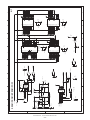
Before installation, unplug the AC power cord from the AC outlet.
6. Unplug the AC power cord from the AC outlet.
1. Open the top cabinet.
7. Remove the IPL ROM from to the IC socket of the MAIN PWB.
2. Set the IPL switch (S1) to the ROM COPY position.
8. Set the IPL switch (S1) to GND position.
ROM COPY
ROM COPY
GND
GND
VCC
VCC
S1
S1
S1
S1
IPL switch
IPL switch
9. Replace the top cabinet.
3. Install the IPL ROM in the IC socket of the MAIN PWB.
10. Perform a master reset.
Turn the mode key switch to the SRV’ position, insert the AC power
cord into the AC outlet.
While holding down the Journal feed key, turn the mode key from
the SRV position to the SRV’ position.
IPL ROM
pin-1
4. Turn the mode key switch to SRV’ position, and insert the AC power
cord into the AC outlet.
5. Turn the mode key switch to SRV position. The IPL procedure is
started.
When the procedure is completed, the message of “Completed” is
shown.
ER-A520U/ER-A530U
IPL FROM EP-ROM
– 21 –
ER-A520U/ER-A530U
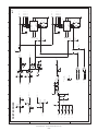
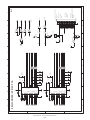
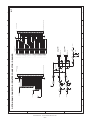
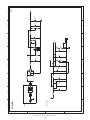
CIRCUIT DIAGRAM AND PWB LAYOUT
– 22 –
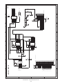
A
B
C
D
7
6
5
27pF
C40
X1
R61
330
SHEN#
8
32.768KHz
PLACE NEAR CPU! !!
C39
18pF
5
5
5
5
CPU
SCK
STH
HTS
KR6#
KR7#
3
3
C49
VCC
2
+
WP#
R83
RPES
JPES
4
4
47K
3 KR8#
R73
R74
VDD
47K
0
117
118
133
134
135
136
137
330pF
2
3.3K
R86
1
3
CST12.0MTW
6 LATCH#
1
2
3
4
C46
C47
C48
8
7
6
5
7
VDD
S0
FSOUT
VSS
FS781
XIN
XOUT
S1
LF
IC3
PLACE NEAR CPU!!!
330pF 330pF 330pF 330pF 330pF
C45
0.1uF
C53
C138
10uF/10V,OS 100pF
C52
R172
100
6
RESET#
5 CKDCR
2 RY/BY#
3 FSR#
3 MODE#
3 KR9#
16
15
19
20
22
8
9
10
11
12
13
14
10K
PHUPS
4
4 VHCOM
VREF
4
138
139
141
144
1
SO
SI
2
3
4
5
6
7
17
18
24
PCLCK
10K
114
10K
R79
R69
47K
VPTEST
TM
R53
25
26
27
28
4,6 STRB4#
10K
R78
R68
47K
4
4
BUZZER
29
30
31
32
33
34
35
36
37
38
40
42
43
44
45
46
47
41
21
57
130
4,6 STRB3#
10K
10K
R77
330pF
330pF
VCC
C43
C42
6 DRAWER2
6 DRAWER1
C3
115
R76
330pF
C41
VCC
R60
10K
POFF#
2,3
10K
DSEN
6
R51
C2
4,6 STRB2#
C54
X2
KR5#
3
R75
6 SI
6 SO
6 PCLK
KR4#
3
R59
10K
KR3#
3
R58
10K
KR2#
+
116
R55
47K
KR1#
3
C1
10uF/10V,OS 10uF/16V 0.1uF
+
93
76
140
142
143
59
74
91
132
39
23
4,6 STRB1#
R54
47K
330pF
C32
R43
10K
VCC
KR0#
3
RXD1
3
CI1#
5
5
TXD1
RS1#
5
RXD2
TXD2
5
5
CI2#
5
5
RS2#
5
R21 R22 R23 R24
10K 10K 10K 10K
NOT USE
VCC
VDD
VDD
P35/A13(MA5)(/D13)
P36/A14(MA6)(/D14)
Vss
Vss
P41/A17(MA9)
5
P125
P106/AN6/KI2
P132
P133
P134
P135
P136
P113
P114
P140
P141
P142
P157
CNVss
VHI30802SB-1(M30802SGP)
P156
P155
BYTE
RESET
P154
P152
Xin
Xout
P151
P153
P146
P150
P145
P144
P137
P131
P112
P143
P130
P111
P127
P124
P105/AN5/KI1
P110
P123
P104/AN4/KI0
P126
P122
P103/AN3
P107/AN7/KI3
P121
P120
P55/HOLD
P54/HLDA/ALE
P56/ALE/RAS
P57/RDY
P53/BCLK/ALE/CLKout
P102/AN2
P101/AN1
P100/AN0
P97/ADtrg/RxD4/SCL4/STxD4
P96/ANEX1/TxD4/SDA4/SRxD4
P95/ANEX0/CLK4
P94/DA1/TB4in/CTS4/RTS4/SS4
P52/RD/DW
P92/TB2in/TxD3/SDA3/SRxD3
P93/DA0/TB3in/CTS3/RTS3/SS3
P50/WRL/WR/CASL
P51/WRH/BHE/CASH
P91/TB1in/RxD3/SCL3/STxD3
P47/CS0/A23
P46/CS1/A22
P87/Xcin
P90/TB0in/CLK3
P45/CS2/A21
P44/CS3/A20(MA12)
P17/D15/INT5
P16/D14/INT4
P15/D13/INT3
P14/D12
P13/D11
P12/D10
P11/D9
P10/D8
P07/D7
P06/D6
P05/D5
P04/D4
P03/D3
P02/D2
P01/D1
P00/D0
P86/Xcout
P85/NMI
P84/INT2
P83/INT1
P82/INT0
P81/TA4in/U
P80/TA4out/U
P77/TA3in
P76/TA3out
P75/TA2in/W
P74/TA2out/W
P73/CTS2/RTS2/TA1in/V
P72/CLK2/TA1out/V
P71/RxD2/SCL2/TA0in/TB5in
P70/TxD2/SDA2/TA0out
P67/TxD1
P66/RxD1
P65/CLK1
P43/A19(MA11)
P42/A18(MA10)
P64/CTS1/RTS1/CTS0/CLKS1
P63/TxD0
P40/A16(MA8)
P62/RxD0
P61/CLK0
P37/A15(MA7)(/D15)
P34/A12(MA4)(/D12)
Vss
P60/CTS0/RTS0
P33/A11(MA3)(/D11)
P32/A10(MA2)(/D10)
Vss
Vss
P31/A9(MA1)(/D9)
P27/A7(/D7)
P30/A8(MA0)(/D8)
Vref
AVss
P26/A6(/D6)
AVcc
Vss
P25/A5(/D5)
P24/A4(/D4)
Vcc
P23/A3(/D3)
P22/A2(/D2)
Vcc
Vcc
P21/A1(/D1)
Vcc
Vcc
P20/A0(/D0)
Vcc
IC1
123
124
125
126
127
128
129
131
48
49
50
51
56
58
60
61
66
67
68
86
87
88
89
90
54
55
53
52
62
63
64
65
69
70
71
72
102
103
104
105
106
107
108
109
110
111
112
113
119
120
121
122
73
75
77
78
79
80
81
82
83
84
85
92
94
95
96
97
98
99
100
101
ER2#
KS 7
KS 6
KS 5
KS 4
KS 3
KS 2
KS 1
KS 0
DR1#
CS1#
CD1#
10K
R87
ER1#
DR2#
CS2#
CD2#
10K
R88
10K
10K
IPLON0#
R67
R62
R52
R46
R45
R44
R42
R41
R40
R39
R38
R37
R36
R35
R34
R33
CHAPTER 7. CIRCUIT DIAGRAM AND PWB LAYOUT
8
33
33
10K
R89
DR1#
CS1#
CD1#
DR2#
CS2#
CD2#
10K
R90
5
5
5
5
5
5
IPLON0 2
VDD
VCC
100
100
100
100
100
100
33
33
33
33
33
33
10K
R91
4
10K
R92
4
10K
R93
10K
R80
33pF
C38
10K
R2
C5
10K
R3
C6
10K
R4
C7
10K
R5
C8
10K
R6
C9
10K
R7
3
C10
10K
R8
C11
10K
R9
C12
10K
R10
C13
5
5
WR#
RD#
47K
LEDS3
LEDS2
LEDS1
10K
3
3
3
3
3
3
3
3
47K
IC34
3 M_RESET#
3
10K
470
R85
3
VCC
10K
C15
10K
R13
C16
10K
R14
C17
10K
R15
C18
10K
R16
10K
R17
C19
2
C20
10K
R18
C21
10K
R19
C22
10K
R20
C23
JDS
JBS
JAS
3
3
VDD
R153
330
0.1uF
C51
R82
22K
DATALE 3
LE
LR/W# 3
LRS
LCDON 3
3
RDS
RBS
RAS
33pF
C26
10K
R28
BLON
33pF
C25
10K
4
4
4
4
4
4
33pF
C27
10K
R29
5
4
C31
C34
10K
R49
C35
10K
R50
C36
D0
D1
D2
D3
D4
D5
D6
D7
6
C50
1000pF
2
74LV00A
IC2B
R71
47K
A21
A20
A22
2
1
R72
12K
3
2
74HC02
IC21A
74LV00A
IC2A
IC2 7Pin : G
ND
14Pin : VD D
2.2K
R70
100pF*4
100pF 100pF 100pF 100pF
C33
10K
33pF*8
33pF 33pF
C30
BUZZER
10K
R32
10K
R48
VCC
33pF
C29
10K
R31
R47
33pF
C28
10K
R30
100pF*10
100pF 100pF 100pF 100pF 100pF 100pF 100pF 100pF 100pF 100pF
C14
R27
10K
R12
VCC
R11
33pF
C24
10K
R26
VCC
R25
KIA7045F
2
1
10K
R66
VCC
10K
R65
47K
10K
R64
VCC
R63
47K
LEDS0
KS3
KS2
KS1
KS0
47K
2,3,6
2,6
47K
R166 R167 R168 R169 R170 R171
100pF*10
100pF 100pF 100pF 100pF 100pF 100pF 100pF 100pF 100pF 100pF
C4
ER2#
ER1#
VCC
NOT USED
10K
R57
10K
R94
10K
R81
VCC
33pF
C37
10K
R56
VCC
10K
R1
VCC
3
Q1
1
+
A20
A21
A22
2048BH
RES#
RESET 5
C2412K
B
BZ1
1SS355
D1
2,3
D [0..7] 2,3,6
A23#
A0
A1
A2
A3
A4
A5
A6
A7
A8
A9
A10
A11
A12
A13
A14
A15
A16
A17
A18
A19
1/7
0.1uF
C44
1
2,3
RESET#
VCC
A[0..22] 2,3,6
1
A
B
C
D
CIRCUIT DIAGRAM AND PWB LAYOUT
– 23 –
A
B
C
D
7
R96
9.1KF
C60
A23#
1,3
8
A19
A20
A21
A22
1,6
1,3,6
1,3,6
1,3
ZD1
UDZ5.1B
VCC
R100
6.2KF
+
NOT USE
1uF/50V
R95
3.9K
+24V
1,3,6 A[0..22]
1,3,6 D[0..7]
2
3
VDD
-
+
1,3
1
C69
0.1uF
P-OFF
IC8A
BA10393 F
R99
10KF
A21
A22
R98
1
56K
A
B
C
G2A
G2B
G1
Y7
GND
IC35
VCC
Y0
Y1
Y2
Y3
Y4
Y5
Y6
9
7
A
B
C
G2A
G2B
G1
Y7
GND
IC6
VCC
Y0
Y1
Y2
Y3
Y4
Y5
Y6
6
5
16
15
14
13
12
11
10
9
-
+
8
VDD
74HC138
IC2 7Pi n : GND
14Pin : VDD
74LV00A
IC2C
74HC138
10
1
2
3
4
5
6
7
8
VLED
1
2
3
4
5
6
7
8
IC8B
BA10393F
R97
2.7K
VCC
A23#
IPLON0
C56
0.1uF
+ C55
10uF/50V
7
16
15
14
13
12
11
10
9
6
6
C68
0.1uF
100p
100p
VDD
C140
1,3
74LV08
IC7D
74LV08
IC7B
74LV08
RAMCS2 #
RAMCS1 #
13
12
5
4
2
1
IC7A
6
3
11
VCC
C57
0.1uF
5
5
FROMCS#
EPROMC S#
RAMCS 3# 6
IC7 7Pi n : GND
14Pin : VCC
C139
POFF#
VCC
C63
1000pF
SRAM / FROM / EPROM / POFF
8
8
4
8
4
ER-A520U/ER-A530U
13
12
74LV00A
IC2D
D0
D1
D2
11
WR#
RES#
A19
A16
A15
A12
A7
A6
A5
A4
A3
A2
A1
A0
1
WP#
1 A19 RY/BY#
A18
A8
A7
A6
A5
A4
A3
A2
1,3,6
1,3
A16
A15
A14
A13
A12
A11
A10
A9
A20
C61
4
VCC
A18/PGM
A17
A14
A13
A8
A9
A11
OE
A10
CE
D7
D6
D5
D4
D3
+
VCC
48
47
46
45
44
43
42
41
40
39
38
37
36
35
34
33
32
31
30
29
28
27
26
25
0.1uF
C70
C67
0.1uF
32
31
30
29
28
27
26
25
24
23
22
21
20
19
18
17
C62
0.1uF
ROM SOCKET( 32Pin)
VPP
A16
A15
A12
A7
A6
A5
A4
A3
A2
A1
A0
D0
D1
D2
GND
IC10
+
VCC
16M FLASH ROM
IPLON0
10uF/50V
C66
1
2
3
4
5
6
7
8
9
10
11
12
13
14
15
16
A16
BYTE
VSS
DQ15/A-1
DQ7
DQ14
DQ6
DQ13
DQ5
DQ12
DQ4
VCC
DQ11
DQ3
DQ10
DQ2
DQ9
DQ1
DQ8
DQ0
OE
VSS
CE
A0
IC4
MBM29F160TE90
A15
A14
A13
A12
A11
A10
A9
A8
A19
NC
WE
RESET
NC
WP
RY/BY
A18
A17
A7
A6
A5
A4
A3
A2
A1
10uF/50V
1
2
3
4
5
6
7
8
9
10
11
12
13
14
15
16
17
18
19
20
21
22
23
24
4
2
A0
3
VCC
3
R104
10K
VCC
A10
EPROMC S#
A18
A17
A14
A13
A8
A9
A11
1,6
1 ROM COPY
SHORTPIN
SP1
D7
D6
D5
D4
D3
VCC
FROMCS#
A1
RD#
D0
D1
D2
D3
D4
D5
D6
D7
A17
3
A18
A16
A14
A12
A7
A6
A5
A4
A3
A2
A1
A0
A18
A16
A14
A12
A7
A6
A5
A4
A3
A2
A1
A0
D0
D1
D2
D0
D1
D2
2
10uF/50V
C64
16
13
14
15
1
2
3
4
5
6
7
8
9
10
11
12
10uF/50V
C58
16
13
14
15
1
2
3
4
5
6
7
8
9
10
11
12
2
D7
D6
D5
D4
D3
RD
A10
CS
VCC
A15
A17
WR
A13
A8
A9
A11
21
20
19
18
17
24
23
22
32
31
30
29
28
27
26
25
D7
D6
D5
D4
D3
RD
A10
CS
VCC
A15
A17
WR
A13
A8
A9
A11
C59
0.1uF
21
20
19
18
17
24
23
22
32
31
30
29
28
27
26
25
+
VDD
C65
0.1uF
4MRAM HY628400A LLT2-70
GND
D0
D1
D2
A18
A16
A14
A12
A7
A6
A5
A4
A3
A2
A1
A0
IC9
+
VDD
4MRAM HY628400A LLT2-70
GND
D0
D1
D2
A18
A16
A14
A12
A7
A6
A5
A4
A3
A2
A1
A0
IC5
VDD
VDD
D7
D6
D5
D4
D3
RD#
WR#
D7
D6
D5
D4
D3
RD#
WR#
2/7
1
1,6
A10
RAMCS2 #
A15
A17
1,3,6
A13
A8
A9
A11
1,6
A10
RAMCS1 #
A15
A17
1,3,6
A13
A8
A9
A11
1
A
B
C
D
ER-A520U/ER-A530U
CIRCUIT DIAGRAM AND PWB LAYOUT
– 24 –
A
B
C
D
8
WR#
A0
A20
A21
A22
A23#
1
KS0
1
KS1
1
KS2
1
KS3
1 M_RESET#
1
LEDS0
1
LEDS1
1
LEDS2
1
LEDS3
1
KR0#
1
KR1#
1
KR2#
1
KR3#
1
KR4#
1
KR5#
1
KR6#
1
KR7#
1
KR8#
1
KR9#
1
MODE#
1
FSR#
1,2,6
1,2,6
1,2,6
1,2,6
1,2
1,2
a
b
c
d
e
f
g
dp
VLED
VCC
0.1uF
C82
C75
0.1uF
LCD I/F / KEY I/F
8
7
VCC
Y0
Y1
Y2
Y3
Y4
Y5
Y6
16
15
14
13
12
11
10
9
6
R106
10K
VCC
6
C76
100pF
1,2,6 D[0..7]
TO POP UP & KEY I/F
C80
100pF
R109
10K
VCC
VCC
52045-4045
KEY I/F R ELAY CN
1
2
3
4
5
6
7
8
9
10
11
12
13
14
15
16
17
18
19
20
21
22
23
24
25
26
27
28
29
30
31
32
33
34
35
36
37
38
39
40
CN1
74HC138
A
B
C
G2A
G2B
G1
Y7
GND
IC14
+ C74
10uF/50V
1
2
3
4
5
6
7
8
9
10
11
12
13
14
KS0
15
KS1
16
KS2
17
KS3
18
M_RESET#
19
LS0
20
LS1
21
LS2
22
LS3
23
KR0
24
KR1
25
KR2
26
KR3
27
KR4
28
KR5
29
KR6
30
KR7
31
KR8
32
KR9
33
MODE# 34
FSR#
35
36
37
38
39
40
1
2
3
4
5
6
7
8
7
DB3
DB1
DB2
DB0
1
D0
D1
D2
D3
D4
D5
D6
D7
C78
0.1uF
D2
D3
D0
D1
DATALE
C73
0.1uF
5
1
2
3
4
5
6
7
8
9
10
1
2
3
4
5
6
7
8
9
10
5
74HC245
DIR
A1
A2
A3
A4
A5
A6
A7
A8
GND
IC16
VCC
Q7
D7
D6
Q6
Q5
D5
D4
Q4
LE
VCC
1G
B1
B2
B3
B4
B5
B6
B7
B8
10uF/50V
+ C77
74HC374
QE
Q0
D0
D1
Q1
Q2
D2
D3
Q3
GND
IC13
+ C72
10uF/50V
D[0. .7]
20
19
18
17
16
15
14
13
12
11
20
19
18
17
16
15
14
13
12
11
VCC
VCC
D5
D4
D7
D6
DB0
DB1
DB2
DB3
DB4
DB5
DB6
DB7
4
DB4
DB5
DB7
DB6
4
DB[0..7]
1
3
BLON
VLED
3
1
D[0..7]
LCDON
1
1
1
R108
10K
1
2
LRS
LR/W#
LE
VCC
IC15
BA00ASFP
D0
D1
D2
D3
D4
D5
D6
D7
3
+
11
1
3
4
7
8
13
14
17
18
Q1
Q2
Q3
Q4
Q5
Q6
Q7
Q8
VCC
2
R111
12K
+
1,2
1,2
a
b
c
d
e
f
g
dp
1
1
22uF/10V,OS
C79
RES#
POFF#
LCD CN(16Pin)5483-16X
LRS
LR/W#
LE
DB0
DB1
DB2
DB3
DB4
DB5
DB6
DB7
1
2
3
4
5
6
7
8
9
10
11
12
13
14
15
16
CN2
R110
2.4KF
R107
5.6K
10
9
*IC 14
VCC:20pin
GND:10pin
2
5
6
9
12
15
16
19
C71
0.1uF
74LV08
IC7C
GND
VCC
C81
22uF/16V
5
4
8
74HC273
CLK
CLR
D1
D2
D3
D4
D5
D6
D7
D8
IC12
2
3/7
A
B
C
D
A
B
C
D
STRB2#
STRB3#
STRB4#
1,6
1,6
1,6
8
STRB1#
VHCOM
1,6
1
PHUPS
1 VPTEST
1
6 TM 1
1SS355
D9
1SS355
D8
1SS355
D7
1SS355
D6
1SS355
D5
C89
R118
1K
4.7K
R114
R112
18KF
VCC
0
R116
7
C95
22uF/16V
1SS355
R126
3.6KF
R122
16KF
1K
D5
VCC
D4
1SS355
R176
R128
1K
VCC
1000pF
C84
100pF
VCC
PRINTER DRIVER
R132
15K
0.1uF
C85
FVHS
6
6
1
R129
5.6K
Q1
2SK2731
+24V
PHUPS1
TM
G
6
D
S
RPES
JPES
Q2
MTD2955V
10K
R127
1
1
6
RAS
RBS
1
JBS
1
1
JAS
1
VCC
C96
0.1uF
VCC
+24V
5
6
3
2
5
12
11
9
8
74HC02
IC21D
74HC02
IC21C
C91
1000pF
10uF/50V
C94
240
R121
BA10393 F
IC17B
7
+24V
BA10393 F
IC17A
1
R117
4.7K
VCC
IC21 7Pi n : GND
14Pin : VCC
T1.6A/25 0V
F1
C92
2200uF/35V
C88
330pF
C83
330pF
R113
4.7K
VCC
5
8
4
8
4
7
FB2
KIA431F
IC19
2
0.1uF
C90
0.1uF
13
10
BFR601009C8NG
R130
20K
3
1
100K
R119
100K
R115
C86
VH
4
4
6
RPES#
JPES#
VREF
1
6
6
FB1
1SS355
D11
BFR601009C8NG
1SS355
D10
+24V
3
3
1
1
JDS
1
R134
1kF
9.1kF
R133
RDS
RAS
R123
1kF
9.1kF
R120
JAS
1
10uF/50V
C93
10uF/50V
C87
RDS
14
5
14
JDS
RAS
5
JAS
+
+
2
INB
INA
INB
INA
2
8
11
2
IC18
1F(1W)
1F(1W)
1F(1W)
R135
11
2
1F(1W)
R136
SMA7036M
SYNCB
SYNCA
IC20
R125
R124
SMA7036M
SYNCB
SYNCA
VS
8
10
15
1
6
OUTB
OUT/B
OUTA
OUT/A
GB
GA
RSB
REFB
REFA
RSA
12
4
9
13
3
7
8
VS
10
15
1
6
OUTB
OUT/B
OUTA
OUT/A
– 25 –
GB
GA
RSB
REFB
REFA
RSA
+
-
CIRCUIT DIAGRAM AND PWB LAYOUT
12
4
9
13
3
7
+
-
ER-A520U/ER-A530U
6
6
6
RPFB#
RPFC#
RPFD#
1
6
RPFA#
JPFD#
6
6
JPFC#
VRCOM
6
6
JPFB#
6
6
4/7
JPFA#
VJCOM
1
A
B
C
D
CIRCUIT DIAGRAM AND PWB LAYOUT
A
B
C
D
7
CD1#
1
ER2#
TxD2
RxD2
CD2#
CI2#
DR2#
CS2#
1
1
1
1
1
1
1
8
RS2#
CS1#
1
1
DR1#
RxD1
1
1
TxD1
1
CI1#
ER1#
1
1
RS1#
1
14
15
16
C101
0.1uF
14
15
16
C111
0.1uF
C113
0.1uF
24
19
22
26
5
8
21
20
6
7
12
24
19
22
26
5
8
21
20
6
7
12
C99
0.1uF
7
IC24
HIN211
/EN
R5OUT
R4OUT
R3OUT
R2OUT
R1OUT
T4IN
T3IN
T2IN
T1IN
C2-
C2+
C1-
C1+
0.1uF
C108
IC23
HIN211
/EN
R5OUT
R4OUT
R3OUT
R2OUT
R1OUT
T4IN
T3IN
T2IN
T1IN
C2-
C2+
C1-
C1+
0.1uF
C97
VCC
VCC
/SHDN
R5IN
R4IN
R3IN
R2IN
R1IN
T4OUT
T3OUT
T2OUT
T1OUT
V-
V+
/SHDN
R5IN
R4IN
R3IN
R2IN
R1IN
T4OUT
T3OUT
T2OUT
T1OUT
V-
V+
C104
25
18
23
27
4
9
28
C119
R146
6
1000p F*5
C115
100oh m*5
R150
R149
R148
R147
5
CS2
DR2
CI2
CD2
RD2
ER2
SD2
C118
C107
100oh m*5
R142
R140
R139
R138
R137
1
C117
C112
10uF/50V
C106
C100
10uF/50V
3
C116
+
VCC
C105
+
VCC
5
RS2
0.1uF
C114
C110
0.1uF
1000p F*5
C103
0.1uF
C102
6
2
17
13
25
18
23
27
4
9
28
1
3
2
17
13
C98
0.1uF
RS232C DRIVER / UP-P16DP CN
8
11
VCC
10
10
11
VCC
10
10
– 26 –
CS1
DR1
CI1
CD1
RD1
SD1
ER1
RS1
4
4
1
1
+24V
F7
1
1
CI1
F2
3
18K
R144
18K
R143
R145
1K
R141
4.7K
9
5
3
1
+
VCC
CI
IC22D
IC22C
IC22B
IC22A
CI2
S1
QCNCM1060AC03
VCC
HTS
10uF/50V
NOT USE
C120
4
SCK
470pF
C109
74HC02
T500mA/250V
VCC
6
IC21B
T500mA/250V(LT5)
SHENA
STHA#
CKDCR
RESET
5
3
1
2
3
ER-A520U/ER-A530U
13
11
2
SHENA
STHA#
HTSA#
SCKA#
RESA
RESA#
ER2
CS2
SD2
RS2
RD2
DR2
CD2
ER1
CS1
SD1
RS1
RD1
DR1
CD1
IC22F
12
10
IC22(74LV14A)
IC22E
8
6
4
2
2
1
2
3
4
5
6
7
8
9
10
11
12
13
14
15
16
17
18
19
20
21
22
23
24
25
26
27
28
29
30
1
1
5/7
FOR UPP16DP
1
FOR ETHERNET(RJ45),UPP16DP,MCR
RELAYPWB
* CN6 24P in-30Pin
CHANN
EL 2
FOR D-SUB 9Pin
* CN6 13P in-20Pin
CHANN
EL 1
FOR D-SUB 9Pin
* CN6 4Pi n-11Pin
* CN6 29Pin
IPL SW
FOR RS232C UP-1 6DP RELAY PWB
52045-3045
CN3
SHEN#
STH
7Pin : GND
14Pin : VCC
HTSA#
SCKA#
RESA
RESA#
1
A
B
C
D
– 27 –
A
B
C
D
7
6
5
8
1 DRAWER2
1 DRAWER1
VDD
1,2,3 D[0..7]
1,2,3 A[0..21]
C136
C137
22uF/16V
7
22uF/16V
D19
6
BFR601009C8NG
Q5
2SD2143
FB30
BFR601009C8NG
2SD2143
FB29
FB28
BFR601009C8NG
R165
1.8K
1SS355
TO OPTION RAM PWB
UP-S02MB
C123
0.1uF
0.1uF
D13
1SR154-400
C121
5
D12
1SR154-400
OPTION RAM STACK CN.35774-4050
F3
Q4
A21
A20
A19
A18
A17
A16
A15
A14
A13
A12
A11
A10
A9
A8
A7
A6
A5
A4
A3
A2
A1
A0
RD#
D7
D6
D5
D4
D3
D2
D1
D0
RAMCS3#
VDD
WR#
1
2
3
4
5
6
7
8
9
10
11
12
13
14
15
16
17
18
19
20
21
22
23
24
25
26
27
28
29
30
31
32
33
34
35
36
37
38
39
40
CN4
T400mA/250V
R164
R152
1SS355
1.8K
R151
+24V
D18
RD#
WR#
2 RAMCS3#
1,2
1,2,3
VCC
FB31
BFR601009C8NG
JPES#
TM1
STRB4#
STRB3#
SO
VH
SI
PCLK
4
4
1,4
1,4
1
4
1
1
RPES#
VRCOM
RPFA#
RPfB#
RPFC#
RPFD#
PHUPS1
FVHS
4
4
4
4
4
4
4
4
R155
2.2K
10K
R153
C124
0.1uF
C122
0.1uF
STRB1#
1,4
STANDARD
DRAWER1
DRAWER2
OPTION
4
C125
1000pF
47K
R154
5046-03A
RIGHT-ANGLE CON
3
2
1
CN7
FB27
FB26
FB25
FB24
FB23
FB22
FB21
FB20
FB19
FB18
FB17
FB16
FB15
FB14
FB13
FB12
FB11
FB10
FB9
FB8
FB7
FB6
FB5
FB4
FB3
EFCB322513TS X 25
4
5046-03A
RIGHT-ANGLE CON
3
2
1
CN6
STRB2#
1,4
LATCH#
JPFD#
1
JPFC#
4
JPFB#
JPFA#
VJCOM
VH
4
4
4
4
4
OPTION RAM CONNECTOR / PRINTER CONNECTOR / DRAWER
8
+
CIRCUIT DIAGRAM AND PWB LAYOUT
+
ER-A520U/ER-A530U
DSEN
1
3
3
VCC
TO PRINTER PR58HM
2
T_PRINTER CN(40Pin)00 6229 640 003 800
40
39
38
37
36
35
34
33
32
31
30
29
28
27
26
25
24
23
22
21
20
19
18
17
16
15
14
13
12
11
10
9
8
7
6
5
4
3
2
1
CN5
2
1
1
6/7
A
B
C
D
CIRCUIT DIAGRAM AND PWB LAYOUT
A
B
C
D
8
[+5V, VLED]
[+24V]
POWER
+24V
F6
7
C133
220uF/50V
T1.0A/250V
CORE
POWERUNIT
7
+
1
IC26
C134
0.01uF
5
2
PQ1CG2032FZ
IC1:HEA T SINK
PS CN
1
2
CN8
C126
M0.033u
6
RB060L40
D17
180uH
IPEAK>2.2A
L2
F4
UL.CSA
3.15A/125V
6
C130
CP301
+
1000uF
/16V
+
BD1
T2A/250V(LT5)
5
PTZ6.2A
ZD3
1SR159-200
D15
F5
5
C127
R163
1KF
3KF
R160
VLED
6800uF/50V
+
1
330uF
/16V
+ C131
1SR159-200
D16
C129
0.1uF
4
VCC +5V
VLED + 5.8V
R158
18K
TP1
VO
4
C132
47uF
/16V
+
5
1
0.1uF
C135
R162
150
VDD
VCC
1
2
CN9
10(FUSE)
R156
D14
3
L1
180uH
RB160L-60
HEAT SINK
3
BT CN(2Pin)5267-02A(BLUE)
Q6
KTD998
LM2574HVN
6,8PIN :NC
7
IC25
R161
180
4
2
3
8
4
– 28 –
3
ER-A520U/ER-A530U
R159
1.2KF
2
R157
22KF
2
+
C128
2200uF/35V
ZD2
PTZ30B
1
1
+24V
7/7
A
B
C
D
PWB LAYOUT
ER-A520U/ER-A530U
CIRCUIT DIAGRAM AND PWB LAYOUT
– 29 –
ER-A520U/ER-A530U
CIRCUIT DIAGRAM AND PWB LAYOUT
– 30 –
ER-A520U/ER-A530U
CIRCUIT DIAGRAM AND PWB LAYOUT
– 31 –
q
COPYRIGHT © 2004 BY SHARP CORPORATION
All rights reserved.
Printed in Japan.
No part of this publication may be reproduced,
stored in a retrieval system, or transmitted.
In any form or by any means,
electronic, mechanical, photocopying, recording, or otherwise,
without prior written permission of the publisher.
SHARP CORPORATION
Digital Document Systems Group
Products Quality Assurance Department
Yamatokoriyama, Nara 639-1186, Japan
2004 March Printed in Japan t