1
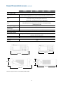
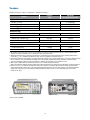
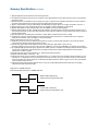
Agilent 53200A Series
RF/Universal Frequency
Counter/Timers
Data Sheet
53210A 350 MHz RF Frequency Counter, 10 digits/sec
53220A 350 MHz Universal Frequency Counter/Timer, 12 digits/sec, 100 ps
53230A 350 MHz Universal Frequency Counter/Timer, 12 digits/sec, 20 ps
Imagine Your Counter Doing More!
Introduction
Frequency counters are depended on in R&D and in manufacturing for the fastest, most accurate frequency and time
interval measurements. The 53200 Series of RF and universal frequency counter/timers expands on this expectation to
provide you with the most information, connectivity and new measurement capabilities, while building on the speed and
accuracy you’ve depended on with Agilent’s decades of time and frequency measurement expertise.
Three available models offer resolution capabilities up to 12 digits/sec frequency resolution on a one second gate. Singleshot time interval measurements can be resolved down to 20 psec. All models offer new built-in analysis and graphing
capabilities to maximize the insight and information you receive.
Measurement by model
More Bandwidth
• 350 MHz baseband frequency
• 6 or 15 GHz optional microwave
channels
More Resolution & Speed
• 12 digits/sec
• 20 ps single-shot time resolution
• Up to 75,000 and 90,000 readings/
sec (frequency and time interval)
More Insight
• Datalog trend plot
• Cumulative histogram
• Built-in math analysis and statistics
• 1M reading memory and USB Flash
storage
More Connectivity
• LXI-C/Ethernet LAN, USB, GPIB
• Optional battery for unstable AC
power or timebase accuracy
More Measurement Capability
(53230A only)
• Continuous gap-free measurements
• Basic measurement and
timestamps for modulation domain
analysis (MDA)
• Optional pulse/burst microwave
measurement
Measurements
Model
Standard
350 MHz Input
Channel(s)
Opt MW Inputs
(53210A: Ch 2,
53220A/30A: Ch 3)
Frequency
53210A,
53220A,
53230A
●
●
Frequency ratio
53210A,
53220A,
53230A
●
●
Period
53210A,
53220A,
53230A
●
●
Minimum/maximum/
peak-to-peak input
voltage
53210A,
53220A,
53230A
●
RF signal strength
53210A,
53220A,
53230A
Single period
53220A,
53230A
●
Time interval A to B, B
to A, A, B
53220A,
53230A
●
Positive/negative
pulse width
53220A,
53230A
●
Rise/fall time
53220A,
53230A
●
Positive/negative duty
53220A,
53230A
●
Phase A to B,
B to A
53220A,
53230A
●
Totalize
(continuous or timed)
53220A,
53230A
●
Continuous/gap-free
53230A
●
●
Timestamp
53230A
●
●
Pulse/burst measurement software1
53230A
(Option 150)
●
●
1. Burst carrier frequency, pulse repetition frequency (PRF), pulse repetition interval (PRI),
burst positive width (“on” time), burst negative width (“off” time).
2
Input Channel Characteristics
53210A
53220A
53230A
Input characteristics (nom)
Channels
Standard (DC - 350 MHz)
Ch 1
Ch 1 & Ch 2
Optional (6 or 15 GHz)
Ch 2
Ch 3
Standard inputs (nom)
Frequency range
DC coupled
DC (1 mHz) to 350 MHz (2.8 ns to 1000 sec)
AC coupled, 50 Ω or 1 MΩ
10 Hz - 350 MHz
1
Input
Connector
Front panel BNC(f). Option 201 adds parallel rear panel BNC(f) inputs2
Input impedance (typ)
Selectable 1 MΩ ± 1.5% or 50 Ω ± 1.5% || <25 pF
Input coupling
Input filter
Selectable DC or AC
Selectable 100 kHz cut-off frequency low pass
10 Hz (AC coupling) cut-off frequency high pass filter
Amplitude range
Input range
±5 V (±50 V) full scale ranges
Sensitivity (typ)
DC - 100 MHz: 20 mVpk
> 100 MHz: 40 mVpk
3,4
Noise3
500 µVrms (max), 350 µVrms (typ)
Input event thresholds
Threshold levels
±5 V (±50 V) in 2.5 mV (25 mV) steps
Selectable On/ Off
Noise reject
4
Slope
Auto-scale
Auto-level
Minimum signal frequency
for auto level
Selectable Positive or Negative
Acquires signal for current measurement channel,
selects range (5 V or 50 V), sets auto-level 50%
Selectable On or Off
On: Sets auto-level (% of Vpp) operation
Occurs once for each INIT or after a timeout.
Measures signal Vpp and sets Trigger level to 50%
Off: Selectable user set level (Volts)
User selectable (Slow (50 Hz), Fast (10 kHz))
Minimum signal for auto
level
300 mVpp
Maximum input
50 Ω damage level
50 Ω protection threshold
1 M Ω damage level
1W
Will not activate below 7.5 Vpk
50 Ω internal termination auto-protects
by switching to 1 M Ω
DC - 5 kHz: 350 Vpk (AC + DC)
5 kHz - 100 kHz: Derate linearly to 10 Vpk (AC + DC)
>100 kHz: 10 Vpk (AC + DC)
3
Input Channel Characteristics continued
53210A
53220A
53230A
Optional microwave inputs (nom)
Frequency range
Option 106
100 MHz - 6 GHz
Option 115
300 MHz - 15 GHz
Input
Connector
Front panel precision Type-N(f)
Option 203 moves the input connector to a rear panel SMA(f)
Input impedance (typ)
50 Ω ± 1.5% (SWR < 2.5)
Input coupling
AC
Continuous wave
amplitude range
Option 106
Autoranged to +19 dBm max. (2 Vrms)
Option 115
Autoranged to +13 dBm max. (1.0 Vrms)
Sensitivity (typ)5
6 GHz (Opt 106): -27 dBm (10 mVrms)
15 GHz (Opt 115):
< 3 GHz: -23 dBm
3 – 11 GHz: -27 dBm
> 11 GHz: -21 dBm
Input event thresholds
Level range
Auto-ranged for optimum sensitivity and bandwidth
50% modulation depth
AM tolerance6
Maximum input
Damage level
6 GHz (Opt 106): > +27 dBm (5 Vrms)
15 GHz (Opt 115): > +19 dBm (2 Vrms)
1. AC coupling occurs after 50 Ω termination.
2. When ordered with optional rear terminals, the standard/baseband channel inputs are active on both the front and rear of the
universal counter though the specifications provided only apply to the rear terminals. Performance for the front terminals with rear
terminals installed is not specified.
3. Multiply value(s) by 10 for the 50 V range.
4. Stated specification assumes Noise Reject OFF. Noise Reject ON doubles the sensitivity minimum voltage levels.
5. Assumes sine wave.
6. CW only. Assumes AM Rate > 10/gate. For Option 106, spec applies for input powers > -20 dBm; use a tolerance of 15% modulation
depth for frequencies less than 900 MHz. For Option 115, spec applies for input powers > -10 dBm.
4
Measurement Characteristics
53210A
53220A
53230A
Measurement range (nom)
Frequency, period (average) measurements
Common
Channels
Ch 1 or optional Ch 2
Digits/s
10 digits/s
12 digits/s
12 digits/s
12 digits
15 digits
15 digits
Reciprocal
Reciprocal and resolution
enhanced
Reciprocal, resolutionenhanced or continuous
(gap-free)
Maximum display
Resolution1
Measurement technique
Signal type
Ch 1, Ch 2 or optional Ch 3
Continuous Wave (CW)
Level & slope
Automatically preset or user selectable
Gate
Gate time2
Advanced gating3
CW and pulse/burst
(Option 150)
Internal or external
1 ms to 1000 s in 10 µs
steps
100 µs to 1000 s in 10 µs
steps
N/A
1 µs to 1000 s in 1 µs steps
Start delay (time or events) and stop hold-off
(time or events)
FM tolerance
± 50%
Frequency, period
DC (1 mHz) to 350 MHz (2.8 ns to 1000 s)
Range9
Microwave input (optional)
Option 106 - 100 MHz to 6 GHz (166 ps to 10 ns)
Option 115 - 300 MHz to 15 GHz ( 66 ps to 3.3 ns)
Frequency ratio4
Range
1015 Displayable range
Timestamp/modulation domain
Sample rate5
N/A
N/A
1 MSa/s, 800 kSa/s,
100 kSa/s, 10 kSa/s
#Edges/timestamp
N/A
N/A
Auto-acquired per
acquisition
Acquisition length
N/A
N/A
up to 1 MSa or
100,000 s (max)
Time interval (single-shot) measurements11
Common
Channels
N/A
Ch 1 or 2
Single-shot time resolution
N/A
Gating
N/A
Internal or external gate
Start delay (time or events) and stop hold-off
(time or events)
Slope
N/A
Independent start, stop slopes
Level
N/A
Independent start, stop slopes
Channel-to-channel time
skew (typ)
N/A
100 ps
100 ps
5
20 ps
50 ps
Measurement Characteristics continued
53210A
53220A
53230A
Time interval A to B, B to A
N/A
-1 ns to 100,000 s (nom)
-0.5 ns to 100,000 s (min)
Range
N/A
2 ns to 100,000 s (min)
Minimum width
N/A
2 ns
Minimum edge repetition
rate
N/A
6 ns
Level & slope
N/A
Auto-level or user selectable
Range9
Time interval A or B
Single-period, pulse-width, rise time, fall time
Range
N/A
0 s to 1000 s
Minimum width
N/A
2 ns
Minimum edge repetition
Rate
N/A
6 ns
Level & slope
N/A
Auto-level or user selectable
Range
N/A
.000001 to .999999 or 0.0001% to 99.9999%
Minumim width
N/A
2 ns
Level & slope
N/A
Auto-level or user selectable
N/A
-180.000º to 360.000º
Channels
N/A
Ch 1 or Ch 2
Range
N/A
0 to 1015 events
Duty
Phase A to B, B to A
Range6
Totalize measurements
9
Rate
N/A
0 - 350 MHz
Gating
N/A
Continuous, timed, or external gate input
Gate accuracy is 20 ns
Level measurements
Voltage level - standard
input channels
Microwave power level
(microwave channel option)
±5.1 Vpk with 2.5 mV resolution or ±51 Vpk with 25 mV resolution
0 to 4 relative signal power
6
Measurement Characteristics continued
53210A
53220A
53230A
6 GHz (Option 106)
15 GHz (Option 115)
12
Pulse/burst frequency and pulse envelope detector (Option 150)
Pulse/burst measurements
N/A
N/A
Carrier frequency, carrier period, pulse repetition interval (PRI),
pulse repetition frequency (PRF), positive and negative width
Pulse/burst width
for carrier frequency
measurements10
N/A
N/A
>200 ns
Narrow: <17 µs
Wide: >13 µs
> 400 ns
Narrow: <17 μs
Wide: >13 μs
Minimum pulse/burst
width for envelope
measurements
N/A
N/A
>50 ns
> 100 ns
Acquisition
N/A
N/A
PRF, PRI range
N/A
N/A
1 Hz – 10 MHz
1 Hz - 5 MHz
Pulse detector response
time (typ)8
N/A
N/A
15 ns rise/fall
40 ns rise/fall
Pulse width accuracy
N/A
N/A
20 ns + (2*carrier period)
75 ns
Power ratio (typ)
N/A
N/A
Power range and
sensitivity (sinusoidal) typ)
N/A
N/A
Auto, Manual7
>15 dB
+13 dBm (1 Vrms) to
-13 dBm (50 mVrms)
< 3 GHz: +7 dBm (500 mVrms) to
-6 dBm (115 mVrms)
3 - 11 GHz: +9 dBm (630 mVrms) to
-8 dBm (90 mVrms)
> 11 GHz: +7 dBm (500 mVrms) to
-6 dBm (115 mVrms)
1. Maximum display resolution for frequency and period. Totalize display resolution is 15 digits, time interval based measurements
are 12 digits.
2. Continuous, gap-free measurements limits the gate time setting to 10 µs to 1000 s in 10 µs steps.
3. Refer to the gate characteristics section for more details on advanced gate capabilities.
4. Measurements on each input channel are performed simultaneously using one gate interval. The actual measurement gate interval
on each channel will be synchrounous with edges of each input signal.
5. Maximum sample rate. Actual sample rate will be limited by the input signal edge rate for signals slower than the selected sample
rate. Maximum timestamp rate offers minimal FM tolerance. If high FM tolerance is required, use lower timestamp rates.
6. Assumes two frequencies are identical, only shifted in phase.
7. Manual control of gate width and gate delay are allowed only for wide pulsed mode.
8. For pulsed signals > -7 dBm (100 mVrms) while gated on.
9. For totalize, time interval and frequency measurements, you may get measurement readings beyond the
range stated, but the accuracy of those readings is not specified.
10. Applies when burst width * Carrier Freq >80.
11. Specifications apply if measurement channels are in 5 V range, DC coupled, 50 Ω terminated and at fixed level for: time interval
single and dual channel, pulse width, duty, phase, single period and rise/fall time measurements.
12. Option 150 microwave pulse/burst measurement descriptions:
-6 dB Detector Level
-12 dB Detector Level
(Option 106 only)
Burst carrier frequency
+ width burst (on)
Burst carrier frequency
+ width burst (on)
- 6 dB
p-p
amplitude
- 12 dB
- width burst (off)
- width burst (off)
PRF
PRI = 1/PRF
PRF
PRI = 1/PRF
7
Gate, Trigger and Timebase Characteristics
53210A
53220A
53230A
Gate characteristics (nom)
Gate
Source
Time, external
Gate time (step size)
1
Time, external or advanced
1 ms - 1000 s (10 µs)
100 µs - 1000 s (10 µs)
1 µs - 1000 s (1 µs)
Advanced: gate start
Source
Slope
Delay time
1
Delay events (edges)
N/A
Internal or external, Ch 1/Ch 2
(unused standard channel input)
N/A
Positive or negative
N/A
0 s to 10 s in 10 ns steps
N/A
0 to 108 for signals up to 100 MHz
N/A
Internal or external, Ch 1/Ch 2
(unused standard channel input)
N/A
Positive or negative
N/A
Hold-off Time settable from 60 ns to 1000 s
N/A
0 to 108 (minimum width (positive or negative) >60 ns)
Advanced: gate stop hold-off
Source
Slope
Hold-off time
1
Hold-off events (edges)
External gate input characteristics (typ)
Connector
Rear panel BNC(f)
Selectable as external gate input or gate output signal
Impedance
1 kΩ when selected as external gate input
Level
TTL compatible
Slope
Selectable positive or negative
Gate to gate timing
3 µs gate end to next gate start
Damage level
<-5 V, >+10 V
Gate output characteristics (typ)
Connector
Rear panel BNC(f)
Selectable as external gate input or gate output signal
Impedance
50 Ω when selected for gate output
Level
TTL compatible
Slope
Selectable positive or negative
Damage level
<-5 V, >+10 V
8
Trigger and Timebase Characteristics (nom)
53210A
53220A
53230A
Trigger characteristics (nom)
General
Trigger source
Internal, external, bus, manual
Trigger count
1 to 1,000,000
Trigger delay
0 s to 3600 s in 1 µs steps
Samples/trigger
1 to 1,000,000
External trigger input (typ)
Connector
Rear panel BNC(f)
Impedance
1 kΩ
Level
TTL compatible
Slope
Selectable positive or negative
Pulse width
> 40 ns min.
Frequency, period: 1 µs + 3 periods
time interval, totalize: 100 ns
Latency2
External trigger rate
300/s max
1 k/s max
Damage level
10 k/s max
<-5 V, >+10 V
Timebase characteristics (nom)
Timebase reference
Internal, external, or auto
Timebase adjustment
method
Closed-box electronic adjustment
Timebase adjustment
Resolution
10-10 (10-11 for Option 010 U-OCXO timebase)
External timebase input (typ)
Impedance
1 kΩ AC coupled
Level (typ)
100 mVrms to 2.5 Vrms
Lock frequencies
10 MHz, 5 MHz, 1 MHz
Lock range
±1 ppm (±0.1 ppm for Option 010 U-OCXO timebase)
Damage level
7 Vrms
Timebase output (typ)
Impedance
50 Ω ± 5% at 10 MHz
Level
0.5 Vrms into a 50 Ω load
1.0 Vrms into a 1 kΩ load
Signal
10 MHz sine wave
Damage level
7 Vrms
1. Continuous, gap-free measurements limits the Gate Time setting to 10 µs to 1000 s in 10 µs steps.
2. Latency does not include delays due to auto-leveling.
9
Math, Graphing and Memory Characteristics (nom)
53210A
53220A
53230A
Math operations
Smoothing (averaging) 1
Selectable 10 (slow), 100 (medium), 1,000 (fast) reading moving average
Selectable filter reset .1% /1000 ppm (fast), .03%/300 ppm (medium), .01%/100 ppm
(slow) change from average
Scaling
mX-b or m(1/X)-b
User settable m and b (offset) values
Δ-change
(X-b)/b scaled to %, ppm, or ppb
User settable b (reference) value
Null
(X-b)
User settable b (reference) value
Statistics 1
Mean, standard deviation,
Max, Min, Peak-to-Peak,
count
Mean, standard deviation, Allan deviation2, Max, Min, Peakto-Peak, count
Limit test 3
Displays PASS/ FAIL message based on user defined Hi/ Lo limit values.
Operation
Individual and simultaneous operation of smoothing, scaling, statistics, and limit test
Graphical display selections
Digits
Numeric result with input level shown
Trend
Strip chart (measurements vs. readings over time)
Selectable screen time
Histogram
Cumulative histogram of measurements; manual reset
HI/LO limit lines shown
Selectable bin and block size
Limit test
Measurement result, tuning bar-graph, and PASS/FAIL message
Markers
Available to read values from trend & histogram displays
Memory
Data log
Instrument state
Guided setup of # of readings/counts;
automatically saves acquisition results to non-volatile memory
Save & recall user-definable instrument setups
Power-off
Automatically saved
Power-on
Selectable power-on to reset (Factory), power-off state or user state
Volatile reading memory
Non-volatile internal
memory
USB file system
Capability
1 M readings (16 MBytes)
75 Mbytes (up to 5 M readings)
Front-panel connector for USB memory device
Store/recall user preferences and instrument states, reading memory,
and bit map displays
10
Speed Characteristics4 (meas)
53210A
Measurement/IO timeout
(nom)
53220A
53230A
no timeout or 10 ms to 2000 s, in 1 ms steps
Auto-level speed
Slow mode (50 Hz): 350 ms (typ)
Fast mode (10 kHz): 10 ms (typ)
Configure-change speed
Frequency, Period, Range, Level: 50 ms (typ)
5
Single measurement throughput : readings/s
(time to take single measurement and transfer from volatile reading memory over I/O bus)
Typical (Avg. using READ?):
LAN (VXI-11)
110
120
LAN (sockets)
200
200
USB
200
200
GPIB
210
220
Optimized (Avg. using *TRG;DATA:REM? 1, WAIT):
LAN (VXI-11)
160
180
LAN (sockets)
330
350
USB
320
350
GPIB
360
420
5
Block reading throughput : readings/s (Example uses: 50,000 readings)
(time to take blocks of measurements and transfer from volatile reading memory over I/O bus)
Typical (Avg. using READ?):
LAN (VXI-11)
300
990
8700
LAN (sockets)
300
990
9700
USB
300
990
9800
GPIB
300
990
4600
Optimized (Avg. using *TRG;DATA:REM? 1, WAIT):
LAN (VXI-11)
300
990
34700
LAN (sockets)
300
990
55800
USB
300
990
56500
GPIB
300
990
16300
11
Speed Characteristics4 (meas) continued
53210A
53220A
53230A
6
Maximum measurement speed to internal non-volatile memory : (readings/s)
Timestamp
Frequency, period, totalize
Frequency ratio
N/A
N/A
1,000,000
75,000
300
44,000
Time interval, rise/fall,
width, burst width
N/A
Duty cycle
N/A
48,000
Phase
N/A
37,000
PRI, PRF
N/A
1000
N/A
90,000
75,000
Transfer from memory to PC via:
LAN (sockets)
600,000 readings/sec
LAN (VXI-11)
150,000 readings/sec
USB
800,000 readings/sec
GPIB
22,000 readings/sec
1. These Math operations do not apply for Continuous Totalize or Timestamp measurements.
2. Allan Deviation is only calculated for Frequency and Period measurements. Allan Deviation calculation is available on both 53220A
and 53230A, it is only gap free on 53230A.
3. Limit Test only displays on instrument front panel. No hardware output signal is available.
4. Operating speeds are for a direct connection to a >2.5 GHz dual core CPU running Windows® XP Pro SP3 or better with 4 GB RAM and
a 10/100/1000 LAN interface.
5. Throughput data based on gate time. Typical reading throughput assumes ASCII format, Auto level OFF with READ? SCPI command. For
improved reading throughput you should also consider setting (FORM:DATA REAL,64), (DISP OFF), and set fastest gate time available.
6. Maximum 53230A rates represent >= 20 MHz input signals with min gate times, no delays or holdoffs. Measurement rates for the
53210A & 53220A are limited by min gate time. Actual meas rates are limited by the repetition rate of the input being measured.
12
General Characteristics (nom)
53210A
53220A
Warm-up time
Display
User interface and help
languages
53230A
45-minutes
4.3" Color TFT WQVGA (480 x 272), LED backlight
English, German, French, Japanese, Simplified Chinese, Korean
USB flash drive
FAT, FAT32
Programming language
SCPI
532xx Series and 53131A/53132A/53181A Series compatibility mode
Programming interface
LXI-C 1.3
USB 2.0 device port
GPIB interface
10/ 100/ 1000 LAN (LAN Sockets and VXI-11 protocol)
USB 2.0 (USB-TMC488 protocol)
GPIB (IEEE-488.1, IEEE-488.2 protocol)
Web user interface
LXI Class C Compatible
Mechanical
Bench dimensions
Rack mount dimensions
Weight
261.1 mm W x 103.8 mm H x 303.2 mm D
212.8 mm W x 88.3 mm H x 272.3 mm D (2U x 2 width)
3.9 kg (8.6 lbs) fully optioned
3.1 kg (6.9 lbs) without Option 300 (battery option)
Environmental
Storage temperature
- 30 °C to +70 °C
Operating environment
EN61010, pollution degree 2; indoor locations
Operating temperature
0 °C to +55 °C
Operating humidity
5% to 80% RH, non-condensing
Operating altitude
Up to 3000 meters or 10,000 ft
Regulatory
Safety
Complies with European Low Voltage Directive and carries the CE-marking
Conforms to UL 61010-1, CSA C22.2 61010-1, IEC 61010-1:2001, CAT I
EMC
Complies with European EMC Directive for test and measurement products.
IEC/EN 61326-1
CISPR Pub 11 Group 1, class A
AS/NZS CISPR 11
ICES/NMB-001
Complies with Australian standard and carries C-Tick Mark
This ISM device complies with Canadian ICES-001
Cet appareil ISM est conforme a la norme NMB-001 du Canada
Acoustic noise (nom)
SPL 35 dB(A)
Line power
Voltage
Power consumption
100V - 240V ± 10%, 50-60 Hz ±5%
100 V - 120 V, 400 Hz ±10%
90 VA max when powered on or charging battery;
6 VA max when powered off/standby
13
General Characteristics (nom) continued
53210A
53220A
53230A
Battery (Option 300)
Technology
Internal lithium ion battery with integrated smart battery monitor & charger
Use for maintaining timebase accuracy or environments with unstable AC power
Operating temperature
limits
0 to 55 °C. Battery will only charge under 35 °C.
Instrument running on battery power above 50 °C
will turn off to minimize battery capacity degradation.
Storage temperature
limits
-10 °C to 60 °C.
Extended exposure to temperatures above 45 °C could degrade battery
performance and life
Operating time (typ)
3 hours when operated below +35 °C
Standby time - OCXO
powered (typ)
24 hours
Recharge time (typ) 1
4 hours to 100% capacity; 2 hours to 90% capacity
Accessories included
CD
User's guide, SCPI/programmers reference, programming examples, drivers (IVI-COM,
LabView), IO library instructions
Cables
Power line cord, 2 m USB 2.0
Warranty
Standard
1 year
1. Assumes calibrated battery.
212.8 mm
261.2 mm
103.8 mm
88.3 mm
272.3 mm
302.2 mm
Dimensions apply to all three models: 53210A, 53220A, 53230A.
14
Timebase
Timebase Uncertainty = ( Aging + Temperature + Calibration Uncertainty )
Standard
TCXO
Timebase
Option 010
Ultra-High Stability OCXO
Aging 1 (spec)
24-hour, TCAL ±1 °C
± 0.3 ppb (typ)
30-day, TCAL ±5 °C
± 0.2 ppm (typ)
± 10 ppb
1-year, TCAL ±5 °C
± 1 ppm
± 50 ppb
2-year, TCAL ±5 °C
± 0.5 ppm
± 25 ppb
± 1 ppm
± 5 ppb
Initial factory calibration (typ)
± 0.5 ppm
± 50 ppb
Settability error
± 0.1 ppb
± 0.01 ppb
5-min. warm-up error 4
± 1 ppm
± 10 ppb
72-hour retrace error
< 50 ppb
< 2 ppb
1 ppb
0.01 ppb
Temperature (typ)
2
0 °C to TCAL - 5 °C and TCAL + 5 °C to 55 °C
Calibration uncertainty
3
Supplemental characteristics (typ)
5
Allan deviation t = 1s
1. All Timebase Aging Errors apply only after an initial 30-days of continuous powered operation and for a constant altitude ±100 m.
After the first 1-year of operation, use ½ x (30-day and 1-year) aging rates shown.
2. Additional temperature error is included in the time base uncertainty equation if the temperature of the operating environment is
outside the TCAL ± 5 °C (calibration temperature) range. The error is applied in its entirety, not per °C.
3. Initial factory calibration error applies to the original instrument calibration upon receipt from the factory. This error is applied until the
first re-calibration occurs after shipment. Settability error is the minimum adjustment increment (resolution) achievable during
electronic adjustment (calibration) of the instrument. It is added to the uncertainty of your calibration source.
4. Warm-up error applies when the instrument is powered on in a stable operating environment.
When moved between different operating environments add the Temperature error during the initial 30-minutes of powered operation
5. Retrace error may occur whenever the instrument line-power is removed or whenever the instrument is battery operated and the
battery fully discharges. Retrace error is the residual timebase shift that remains 72-hours after powering-on an instrument that has
experienced a full power-cycle of the timebase. Additional frequency shift errors may occur for instrument exposure to severe
impact shocks >50 g.
Front/rear view of 53230A
15
Accuracy Specifications
Definitions
Random Uncertainty
The RSS of all random or Type-A measurement errors expressed as the total RMS or 1-σ measurement uncertainty. Random
uncertainty will reduce as 1/√N when averaging N measurement results for up to a maximum of approximately 13-digits or 100 fs.
Systematic Uncertainty
The 95% confidence residual constant or Type-B measurement uncertainty relative to an external calibration reference.
Generally, systematic uncertainties can be minimized or removed for a fixed instrument setup by performing relative measurements to
eliminate the systematic components.
Timebase Uncertainty
The 95% confidence systematic uncertainty contribution from the selected timebase reference. Use the appropriate uncertainty for the
installed timebase or when using an external frequency reference substitute the specified uncertainty for your external frequency
reference.
Basic accuracy 1 = ± [(k * Random Uncertainty) + Systematic Uncertainty + Timebase Uncertainty]
Measurement Function
1-σ Random Uncertainty
Systematic Uncertainty
Timebase
Uncertainty2
Frequency 3
Period (parts error)
1.4* (TSS2 + TE2)2
If RE ≥ 2: 10 ps / gate (max), 2 ps / gate (typ)4
If RE < 2 or REC mode (RE = 1): 100 ps / gate
●
Option 106 & 115:
Frequency 3
Period (parts error)
1.4* (TSS2 + TE2)2
RE * gate
If RE ≥ 2: 10 ps / gate (max), 2 ps / gate (typ)4
If RE < 2 : 100 ps / gate
Frequency Ratio A/B (typ) 5
(parts error)
1.4* Random Uncertainty
of the worst case Freq input
Uncertainty of Frequency A plus Uncertainty
of Frequency B
Single Period
(parts error)17
1.4* (TSS 2 + TE2) 2
Taccuracy
Period Measurement
Period Measurement
1.4* (TSS 2 + TE2) 2
Linearity 6 + Offset 8
|TI Measurement|
|TI Measurement|
Time Interval (TI)17, Width 17, or
Rise/Fall Time 7, 17 (parts error)
RE * gate
Linearity = Taccuracy
Offset (typ) = TLTE + skew + Taccuracy
Duty
(fraction of cycle error)
2 2
2* (TSS + TE ) * Frequency
(TLTE + 2*Taccuracy)*Frequency
Phase 5, 9, 17 (Degrees error)
2* (TSS 2 + TE2) 2 * Frequency
* 360º
(TLTE+skew+2*Taccuracy)*Frequency*360º
Totalize11 (counts error)
± 1 count11
5, 9, 10, 17
Volts pk to pk (typ)
5 V range
12
2
DC, 100 Hz - 1 kHz: 0.15% of reading + 0.15% of range
1 kHz - 1 MHz: 2% of reading + 1% of range
1 MHz - 200 MHz: 5% of reading + 1% of range
+ 0.3 * (Freq/250 MHz) * reading
16
●
●
●
Accuracy Specifications continued
Measurement Function
1-σ Random Uncertainty
Systematic Uncertainty
Timebase
Uncertainty2
6 GHz (Option 106): Optional Microwave Channel Opt 150 - Pulse/Burst Measurements3, 13
PRF, PRI (parts error) 14
Pulse/Burst Carrier Frequency 15
(Narrow Mode) (parts error)
Pulse/Burst Carrier Frequency 16
(Wide Mode) (parts error)
If RE = 1: 500 ps / gate
200 ps
RE * gate
100 ps
200 ps
Burst Width
Burst Width
40 ps
100 ps
RE * Burst Width
RE * Burst Width
If RE > 1: 200 ps / (RE * gate)
●
●
●
15 GHz (Option 115): Optional Microwave Channel Opt 150 - Pulse/Burst Measurements3, 13
PRF, PRI (parts error) 14
Pulse/Burst Carrier Frequency 15
(Narrow Mode) (parts error)
Pulse/Burst Carrier Frequency 16
(Wide Mode) (parts error)
1 ns
(RE * gate)
200 ps
RE * gate
100 ps
400 ps
Burst Width
Burst Width
75 ps
200 ps
RE * Burst Width
RE * Burst Width
17
●
●
●
Accuracy Specifications continued
1. Apply the appropriate errors detailed for each measuring function.
2. Use Timebase Uncertainty in Basic Accuracy calculations only for Measurement Functions that show the ● symbol in the Timebase
Uncertainty column.
3. Assumes Gaussian noise distribution and non-synchronous gate, non-gaussian noise will effect Systematic Error. Note all optional
microwave channel specifications (continuous wave and pulse/burst) assume sine signal.
4. Typical is achieved with an average of 100 readings with 100 samples per trigger. Worst case is trigger and sample count set to 1.
5. Improved frequency ratio, duty and phase specifications are possible by making independent measurements.
6. Minimum Pulse Width for using stated linearity is 5 ns; Pulse Widths of 2-5 ns use linearity=400 ps.
7. Residual instrument Rise/ Fall Time 10%-90% 2.0 ns (typ). Applies to fixed level triggering. Threshold can still be set based on % of
auto-level detected peaks, but since these peak levels may contain unknown variations, accurate measurements need to be based on
absolute threshold levels.
8. Input signal slew rates and settling time have effects on offset. Offset is calibrated with rise times < 100 ps.
9. Constant Duty or Phase are required during the measurement interval. Duty and Phase are calculated based on two automated
sequential measurements - period and width or TI A to B, respectively.
10. Duty is represented as a ratio (not as a percent).
11. Additional count errors need to be added for gated totalize error, latency or jitter. If gated, add gate accuracy term (See Totalize
measurements in the Measurement Characteristics section).
12. Volts pk error apply for signal levels between full range and 1/10th range. Spec applies to sine wave only.
50 V range reading accuracy is 2% at DC-1 KHz, 5% 1 KHz -1 MHz band. Accuracy above 200 MHz is not specified on both ranges.
13. For 6 GHz (Opt 106): Specifications apply to signals from ±13 dBm, operable to ±19 dBm. For 15 GHz (Opt 115): Specifications apply to
input powers as listed under “Pulse/burst frequency and pulse envelope detector (Option 150) measurement characteristics”,
operable from +13 dBm to -8 dBm.
14. Use the RE equation, but use the input PRF for FIN. Assume sharp envelope transition.
15. Applies when Burst Width * Carrier Freq > 80.
16. Specifications based on gate and width for automated detection. If in manual mode, delay and width selected will impact accuracy
specification. For approximate accuracy for manual gate, use the RE calculation, but FIN is now 106 and use gate as burst width. For
input signals where PRI < 250 μs, double the 1-σ Random Uncertainty specification, unless a Trigger Count of 1 and a large Sample
Count acquisition method are used.
17. Specifications apply if measurement channels are in 5 V range, DC coupled, 50Ω terminated and at fixed level. The following
minimum pulse width requirements apply:
Single-Period: <250 MHz, 50% Duty
Phase, Dual Channel Time Interval: <160 MHz, 50% Duty
> 2 ns
> 4 ns
> 2 ns
> 4 ns
Negative width, Negative duty,
Single Channel Time Interval Fall to Rise
Positive width, Positive duty,
Single Channel Time Interval Rise to Fall
18
Definition of Measurement Error Sources and Terms used in Calculations
53210A
53220A
53230A
RE
1
use RE equation
use RE equation
TSS
100 ps
100 ps
20 ps
Skew
100 ps
50 ps
Taccuracy
200 ps
100 ps
Confidence Level (k)
For 99% Confidence use k= 2.5 in accuracy calculations.
For 95% Confidence use k= 2.0 in accuracy calculations.
Resolution enhancement factor (RE)
The resolution enhancement (RE) calculates the added frequency resolution beyond the basic reciprocal measurement
capability that is achieved for a range of input signal frequencies and measurement gate times. The maximum enhancement factor shown is for input signals where TSS > TE and is limited due to intrinsic measurement limitations. For signals
where TSS << TE, RE may be significantly higher than the specified levels. RE will always be >=1.
For signals where TSS >> TE, RE = √(FIN * Gate/16) RE is limited by gate time as show below
Gate time > 1 s, RE max of 6
Gate time 100 ms, RE max of 4
Gate time 10 ms, RE max of 2
Gate time < 1 ms, RE = 1
Interpolation between listed gate times allowed.
Single shot timing (TSS)
Timing resolution of a start/stop measurement event.
Skew
Skew is the additional time error if two channels are used for a measurement. It is not used for width, rise/fall time, and
single channel time interval.
Taccuracy
Taccuracy is the measurement error between two points in time.
Threshold error (TE)
Threshold error (TE) describes the input signal dependent random trigger uncerFor 5v (500µV2 + EN2+Vx2)2
tainty or jitter. The total RMS noise voltage divided by the input signal slew rate
SR-TRIG POINT
(V/s) at the trigger point gives the RMS time error for each threshold crossing.
For simplicity TE used in the Random Uncertainty calculations is the worst TE
of all the edges used in the measurement. RSS of all edge’s TE is an acceptable
For 50v (5000µV2 + EN2+Vx2)2
alternative. Vx is the cross talk from the other standard input channel. Typically
this is -60 dB. Vx = 0 on 53210A, and when no signal is applied to other stanSR-TRIG POINT
dard input channel on 53220A/53230A. (Note: the best way to eliminate cross
talk is to remove the signal from the other channel).
Threshold level timing error (TLTE)
This time interval error results from trigger level setting errors and input hyster± TLSE-start ± TLSE-stop ± 2 VH - 2 VH
esis effects on the actual start and stop trigger points and results in a combined
SR-start SR-stop SR-start SR-stop
time interval error. These errors are dependant on the input signal slew rate at
each trigger point.
VH = 20 mV hysteresis or 40 mV when Noise Reject is turned ON. Double VH values for frequencies > 100 MHz.
[
19
]
Definition of Measurement Error Sources and Terms
used in Calculations continued
Phase Noise and Allan Deviation
The input signal’s jitter spectrum (Phase noise) and low-frequency wander characteristics (Allan variation) will limit the achievable measurement resolution and
accuracy. The full accuracy and resolution of the counter can only be achieved
when using a high-quality input signal source or by externally filtering the input
signal to reduce these errors.
Threshold level setting error (TLSE)
Threshold level setting error (TLSE) is the uncertainty in the actual signal threshold point due to the inaccuracies of the threshold circuitry.
Slew rate (SR)
Slew rate (SR) describes the input signal’s instantaneous voltage rate of change
(V/s) at the chosen threshold point at customer BNC.
For sine wave signals, the maximum slew rate SR= 2πF*V0 to PK.
For Square waves and pulses, the max slew rate = 0.8 Vpp/ tRISE 10-90
Using the 100 kHz low pass filter will effect Slew Rate.
Signal noise (EN)
The input signal RMS noise voltage (EN) measured in a DC - 350 MHz bandwidth.
The input signal noise voltage is RSS combined with the instruments equivalent
input noise voltage when used in the Threshold Error (TE)
calculation.
20
±(0.2%-of setting + 0.1%-of range)
V/s (at threshold point)
Ordering Information
Model numbers
53210A 350 MHz, 10-digits/s RF Frequency Counter
53220A 350 MHz, 12 digits/s, 100 ps Universal Frequency Counter/Timer
53230A 350 MHz, 12-digits/s, 20 ps Universal Frequency Counter/Timer
All models include:
• Certificate of Calibration and 1-year standard warranty
• IEC Power Cord, USB cable
• CD including: Programming Examples, Programmer's Reference Help File,
User's Guide, Quick Start Tutorial, Service Guide
• Agilent IO Library CD
Available options
Option 010 Ultra-high-stability OCXO timebase
Option 106 6 GHz microwave input
Option 115 15 GHz microwave input
Option 150 Pulse microwave measurements (53230A only)
Option 201 Add rear panel parallel inputs for baseband channels1
Option 202 Optional microwave input - front Type N
(default if 106 or 115 ordered)
Option 203 Optional microwave input - rear panel SMA(f) connector
Option 300 Add internal lithium ion smart battery and charger for unstable
AC power or timebase stability
Recommended accessories2
1250-1476 BNC(f) to type-N adapter
N2870A
Passive probe, 1:1, 35 MHz, 1.3 m
N2873A
Passive probe, 10:1, 500 MHz, 1.3 m
N2874A
Passive probe, 10:1, 1.5 GHz, 1.3 m
34190A
Rack mount kit; Use for mounting one 2U instrument by itself,
without another instrument laterally next to it. Includes one
rack flange and one combination rack flange-filler panel.
34191A
2U dual flange kit; Use for mounting two 2U instruments
side-by-side. Includes two standard rack flanges. Note:
Mounting two instruments side-by-side will require the 34194A
Dual-lock link kit and a shelf for the instruments to sit on.
34194A
Dual-lock link kit; for side-by-side combinations of instruments,
and includes links for instruments of different depths.
34131A
Transit case
Support options
3-year Extended warranty
5-year Extended warranty
3-year Annual calibration service
5-year Annual calibration service
1. When ordered with optional rear terminals, the standard/baseband channel inputs
are active on both the front and rear of the universal counter though the specifications
provided only apply to the rear terminals. Performance for the front terminals with rear
terminal options is not specified.
2. All probes must be compatible with a 20 pf input capacitance.
21
Appendix A - Worked Example
Basic Accuracy Calculation for Frequency Measurement
Parameter assumptions:
• 53220A
• 95% confidence
• 100 MHz signal, 1 sec gate
• AUTO frequency mode
• Level: 5 V input signal amplitude
• TCXO standard timebase for unit plugged in for 30 days
• Assume operating temperature is within TCAL ± 5 °C
• Instrument has been re-calibrated so Factory Calibration Uncertainty term is not required.
Process:
Basic accuracy = ± [(k * Random Uncertainty) + Systematic Uncertainty + Timebase Uncertainty]
1. Use k=2 for 95% confidence and k=2.5 for 99% confidence calculations)………………..k = 2
2. Random uncertainty for frequency measurement =
TSS = 100 ps
=
TE (for 5 V)
(500 μV2 + EN2+Vx2)2
SR-TRIG POINT
1.4* (TSS2 + TE2)2
RE * Gate Time
=
(500 μV2)2
3.14 * 109
=
=
1.4* (100ps2 + .159ps2)2
6*1s
=
23.3 E-12
parts error
.159 ps
EN = Assume input signal RMS noise voltage is 0.
Vx = N/A (remove signal from other channel)
SR-TRIG POINT = maximum slew rate (sine)SR= 2πF*V0 to PK = 2π(100 MHz)*5 V = 3.14*109 Volts/Hz
Since TSS >> TE, we use the RE equation. Value is much greater than 6. so we limit RE to 6 due to gate time. RE = 6
Gate time = 1 sec
3. Systematic uncertainty for frequency measurement = If RE >= 2: 10 ps/gate max, 2 ps/gate (typ) = 2 E-12 parts error
0.2 E-6
4. Timebase uncertainty = aging = 0.2 ppm =
parts error
Aging: 0.2 ppm
Basic accuracy = ± [(k * random uncertainty) + systematic uncertainty + timebase uncertainty] =
± [(2 * (23.3 E-12)) + 2 E-12 + 0.2 E-6] = ± 0.2 E-6 parts error
Note: Using a higher accuracy timebase or locking to an external timebase standard will have the biggest impact on
improvement to accuracy calculations.
22
Definitions
The following definitions apply to the specifications and characteristics described throughout.
Specification (spec)
The warranted performance of a calibrated instrument that has been stored for a minimum of 22 hours within the operating
temperature range of 0 °C - 55 °C and after a 45-minute warm up period. Automated calibration (*CAL?) performed within ±5 °C before
measurement. All speciications were created in compliance with ISO-17025 methods.
Data published in this document are speciications unless otherwise noted.
Typical (typ)
The characteristic performance, which 80% or more of manufactured instruments will meet. This data is not warranted, does not
include measurement uncertainty, and is valid only at room temperature (approximately 23 °C). Automated calibration (*CAL?)
performed within ±5 °C before measurement.
Nominal (nom)
The mean or average characteristic performance, or the value of an attribute that is determined by design such as a connector type,
physical dimension, or operating speed. This data is not warranted and is measured at room temperature (approximately 23 °C).
Automated calibration (*CAL?) performed within ±5 °C before measurement.
Measured (meas)
An attribute measured during development for purposes of communicating the expected performance.
This data is not warranted and is measured at room temperature (approximately 23 °C).Automated calibration (*CAL?) performed within
±5 °C before measurement.
Stability
Represents the 24-hour, ±1 °C short-term, relative measurement accuracy.
Includes measurement error and 24-hour ± 1°C timebase aging error.
Accuracy
Represents the traceable measurement accuracy of a measurement for TCAL ± 5 °C. Includes measurement error, timebase error, and
calibration source uncertainty.
Random measurement errors are combined using the root-sum-square method and are multiplied by K for the desired conidence level.
Systematic errors are added linearly and include time skew errors, trigger timing errors, and timebase errors as appropriate for each
measurement type.
TCAL
Represents the ambient temperature of the instrument during the last adjustment to calibration reference standards.
TCAL must be between 10 °C to 45 °C for a valid instrument calibration.
TACAL
Represents the temperature of the instrument during the last automated calibration (*CAL?) operation.
All information in this document are subject to change without notice.
23
www.agilent.com
www.agilent.com/find/frequencycounters
myAgilent
myAgilent
For more information on Agilent
Technologies’ products, applications or
services, please contact your local Agilent
office. The complete list is available at:
www.agilent.com/find/contactus
www.agilent.com/find/myagilent
A personalized view into the information most relevant to you.
www.axiestandard.org
AdvancedTCA® Extensions for Instrumentation and Test (AXIe)
is an open standard that extends the AdvancedTCA for general
purpose and semiconductor test. Agilent is a founding member of
the AXIe consortium.
Americas
Canada
Brazil
Mexico
United States
(877) 894 4414
(11) 4197 3600
01800 5064 800
(800) 829 4444
Asia Pacific
PCI eXtensions for Instrumentation (PXI) modular instrumentation
delivers a rugged, PC-based high-performance measurement and
automation system.
Australia
China
Hong Kong
India
Japan
Korea
Malaysia
Singapore
Taiwan
Other AP Countries
Three-Year Warranty
Europe & Middle East
www.agilent.com/find/ThreeYearWarranty
Belgium
Denmark
Finland
France
www.lxistandard.org
LAN eXtensions for Instruments puts the power of Ethernet and the
Web inside your test systems. Agilent is a founding member of the
LXI consortium.
www.pxisa.org
Agilent’s combination of product reliability and three-year warranty
coverage is another way we help you achieve your business goals:
increased confidence in uptime, reduced cost of ownership and
greater convenience.
Agilent Advantage Services
www.agilent.com/find/AdvantageServices
Accurate measurements throughout the life of your instruments.
www.agilent.com/quality
Agilent Electronic Measurement Group
DEKRA Certified ISO 9001:2008
Quality Management System
Germany
Ireland
Israel
Italy
Netherlands
Spain
Sweden
United Kingdom
1 800 629 485
800 810 0189
800 938 693
1 800 112 929
0120 (421) 345
080 769 0800
1 800 888 848
1 800 375 8100
0800 047 866
(65) 375 8100
32 (0) 2 404 93 40
45 45 80 12 15
358 (0) 10 855 2100
0825 010 700*
*0.125 €/minute
49 (0) 7031 464 6333
1890 924 204
972-3-9288-504/544
39 02 92 60 8484
31 (0) 20 547 2111
34 (91) 631 3300
0200-88 22 55
44 (0) 118 927 6201
For other unlisted countries:
Agilent Channel Partners
www.agilent.com/find/contactus
www.agilent.com/find/channelpartners
(BP-09-27-13)
Get the best of both worlds: Agilent’s measurement expertise and
product breadth, combined with channel partner convenience.
Product specifications and descriptions in
this document subject to change without
notice.
© Agilent Technologies, Inc. 2013
Published in USA, October 16, 2013
5990-6283ENEN