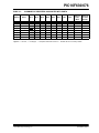
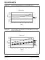
1
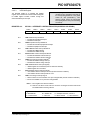
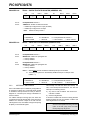
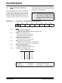
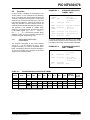
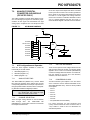
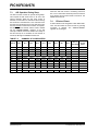
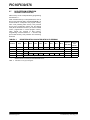
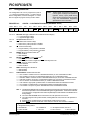
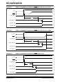
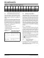
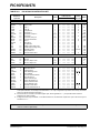
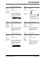
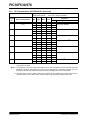
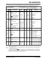
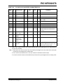
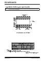
PIC16F630/676 8.1 EEADR The EEADR register can address up to a maximum of 128 bytes of data EEPROM. Only seven of the eight bits in the register (EEADR<6:0>) are required. The MSb (bit 7) is ignored. The upper bit should always be ‘0’ to remain upward compatible with devices that have more data EEPROM memory. 8.2 EECON1 AND EECON2 REGISTERS of the read or write operation. The inability to clear the WR bit in software prevents the accidental, premature termination of a write operation. The WREN bit, when set, will allow a write operation. On power-up, the WREN bit is clear. The WRERR bit is set when a write operation is interrupted by a MCLR Reset, or a WDT Time-out Reset during normal operation. In these situations, following Reset, the user can check the WRERR bit, clear it, and rewrite the location. The data and address will be cleared, therefore, the EEDATA and EEADR registers will need to be re-initialized. EECON1 is the control register with four low order bits physically implemented. The upper four bits are nonimplemented and read as ‘0’s. The Interrupt flag bit EEIF in the PIR1 register is set when the write is complete. This bit must be cleared in software. Control bits RD and WR initiate read and write, respectively. These bits cannot be cleared, only set, in software. They are cleared in hardware at completion EECON2 is not a physical register. Reading EECON2 will read all ‘0’s. The EECON2 register is used exclusively in the data EEPROM write sequence. REGISTER 8-3: EECON1 — EEPROM CONTROL REGISTER (ADDRESS: 9Ch) U-0 U-0 U-0 U-0 R/W-x R/W-0 R/S-0 R/S-0 — — — — WRERR WREN WR RD bit 7 bit 0 bit 7-4 Unimplemented: Read as ‘0’ bit 3 WRERR: EEPROM Error Flag bit 1 = A write operation is prematurely terminated (any MCLR Reset, any WDT Reset during normal operation or BOD detect) 0 = The write operation completed bit 2 WREN: EEPROM Write Enable bit 1 = Allows write cycles 0 = Inhibits write to the data EEPROM bit 1 WR: Write Control bit 1 = Initiates a write cycle (The bit is cleared by hardware once write is complete. The WR bit can only be set, not cleared, in software.) 0 = Write cycle to the data EEPROM is complete bit 0 RD: Read Control bit 1 = Initiates an EEPROM read (Read takes one cycle. RD is cleared in hardware. The RD bit can only be set, not cleared, in software.) 0 = Does not initiate an EEPROM read Legend: S = Bit can only be set DS40039F-page 52 R = Readable bit W = Writable bit U = Unimplemented bit, read as ‘0’ - n = Value at POR ’1’ = Bit is set ’0’ = Bit is cleared x = Bit is unknown 2010 Microchip Technology Inc.