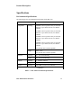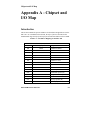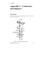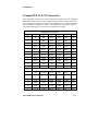
1
EPC -100 Hardware Reference RadiSys Corporation 5445 NE Dawson Creek Drive Hillsboro, OR 97124 Phone: (503) 615-1100 Fax: (503) 615-1150 http://www.radisys.com _____________________________________________________________________ 07-0930-00 August 1997 EPC-100 Hardware Reference Ray-O-Vac is a registered trademark of Ray-O-Vac, Inc. Portions of this manual are Copyright 1993-1994 Cirrus Logic, Inc. IBM, OS/2, and PC/AT are trademarks of International Business Machines Corporation. Intel and Pentium are registered trademarks of Intel Corp. Microsoft and MS-DOS are registered trademarks of Microsoft Corporation. PhoenixBIOS and NuBIOS are trademarks of Phoenix Technologies, Ltd. RadiSys and EPC are registered trademarks and EPConnect is a trademark of RadiSys Corporation. All other trademarks and registered trademarks are the property of their respective owners. August 1997 Copyright 1994, 1995, 1996, 1997 by RadiSys Corporation All rights reserved. Page ii EPC-100 Hardware Reference Table of Contents Chapter 1 - Product Description........................................................................1-1 About this Manual ........................................................................................1-1 Overview ......................................................................................................1-3 cPCI bus ......................................................................................................1-4 cPCI Device Interface ..........................................................................1-5 Specifications ...............................................................................................1-6 Environmental Specifications ..............................................................1-6 Other Specifications.............................................................................1-8 Chapter 2 - Installation.......................................................................................2-1 Introduction ..................................................................................................2-1 Inserting the EPC-100...................................................................................2-2 Removing the EPC-100 ................................................................................2-2 Configuring the EPC-100 .............................................................................2-2 Connecting Peripherals to the EPC-100...............................................2-2 SCSI Termination ................................................................................2-3 System Software Installation ........................................................................2-3 Operating System Software..................................................................2-3 Video Driver Software .........................................................................2-3 Ethernet Software.................................................................................2-3 Chapter 3 - BIOS Configuration........................................................................3-1 Introduction ..................................................................................................3-1 BIOS Setup Screens......................................................................................3-1 Main Setup Menu .........................................................................................3-3 System Time:/System Date:.................................................................3-3 Diskette A:/Diskette B: ........................................................................3-3 IDE Adapter 0/1 Master/Slave: Sub-menus .........................................3-3 Video System:......................................................................................3-4 Memory Cache Sub-menu....................................................................3-4 Memory Shadow Sub-menu.................................................................3-4 Boot Sequence Sub-menu ....................................................................3-4 Keyboard Features (Numlock) Sub-menu............................................3-4 System Memory ...................................................................................3-4 Extended Memory................................................................................3-4 Page iii EPC-100 Hardware Reference IDE Adapter Sub-menu ................................................................................3-5 Type .....................................................................................................3-6 Multi-Sector Transfers .........................................................................3-6 LBA Mode Control ..............................................................................3-6 32-bit I/O..............................................................................................3-6 Transfer Mode......................................................................................3-7 Boot Options Sub-menu................................................................................3-8 Boot Delay: ..........................................................................................3-8 Boot Sequence:.....................................................................................3-8 Setup Prompt:.......................................................................................3-9 POST Errors:........................................................................................3-9 Floppy Check: ......................................................................................3-9 Summary Screen: .................................................................................3-9 Extended Memory Test:.......................................................................3-9 Keyboard Features Menu..............................................................................3-10 Numlock...............................................................................................3-10 Key Click: ............................................................................................3-10 Keyboard auto-repeat rate: ...................................................................3-10 Keyboard auto-repeat delay: ................................................................3-11 Advanced Menu............................................................................................3-12 Integrated Peripherals Sub-menu .........................................................3-12 Advanced Chipset Control Sub-menu ..................................................3-12 Plug & Play OS ....................................................................................3-13 Reset Configuration Data .....................................................................3-13 Halt on watchdog reset.........................................................................3-13 Watchdog Timer Interrupt....................................................................3-13 Large Disk Access Mode: ....................................................................3-13 User BIOS Extensions..........................................................................3-13 BIOS Extension Offset in FBD:...........................................................3-14 Destination Address: ............................................................................3-14 BIOS Extension Size:...........................................................................3-14 Integrated Peripherals Sub-menu..................................................................3-15 COM A port .........................................................................................3-15 COM B port .........................................................................................3-15 LPT port ...............................................................................................3-16 LPT Mode ............................................................................................3-16 Diskette Controller ...............................................................................3-16 Local Bus IDE adapter .........................................................................3-16 Onboard Ethernet controller.................................................................3-16 Onboard SCSI controller......................................................................3-16 Page iv EPC-100 Hardware Reference Advanced Chipset Control Sub-menu...........................................................3-17 DRAM Speed.......................................................................................3-17 DMA Aliasing......................................................................................3-17 8-bit I/O Recovery ...............................................................................3-18 16-bit I/O Recovery .............................................................................3-18 IRQ 12 used by ....................................................................................3-18 ECC/Parity Config ...............................................................................3-18 Memory Cache Sub-menu ............................................................................3-19 Internal Cache ......................................................................................3-19 External Cache .....................................................................................3-19 Cache System BIOS Area ....................................................................3-19 Cache Video BIOS Area ......................................................................3-20 Cache Memory Regions.......................................................................3-20 Memory Shadow Sub-menu .........................................................................3-21 System Shadow....................................................................................3-21 Video Shadow......................................................................................3-21 Shadow Memory Regions....................................................................3-22 Power Management Menu............................................................................3-23 APM.....................................................................................................3-23 Power Savings......................................................................................3-23 Standby Timeout..................................................................................3-24 Suspend Timeout..................................................................................3-24 Standby CPU Speed.............................................................................3-24 Fixed Disk Timeout .............................................................................3-24 CRT......................................................................................................3-24 Standby Timer Reset Events ................................................................3-24 Standby Break Events ..........................................................................3-25 Standby Wakeup Events.......................................................................3-27 Exit Menu .....................................................................................................3-28 Save Changes & Exit ...........................................................................3-28 Exit Without Saving Changes ..............................................................3-28 Get default values ................................................................................3-28 Backup CMOS to Flash .......................................................................3-29 Restore CMOS from Flash...................................................................3-29 Restore CMOS Condition ....................................................................3-29 Load previous values............................................................................3-29 Save Changes.......................................................................................3-29 Exit & Update BIOS ............................................................................3-29 Page v EPC-100 Hardware Reference Chapter 4 - Theory of Operation .......................................................................4-1 Introduction ..................................................................................................4-1 Block Diagram..............................................................................................4-2 Processor Module Daughterboard.................................................................4-2 Cache Memory .............................................................................................4-2 Main System Memory ..................................................................................4-2 Upgrading Main System Memory.................................................................4-4 Memory Map ................................................................................................4-4 Interrupt Usage .............................................................................................4-5 Watchdog Timer ...........................................................................................4-6 Flash Boot Device.........................................................................................4-7 Keyboard/Mouse Controller .........................................................................4-7 BIOS ROM and ROM Shadowing................................................................4-8 CMOS Save and Restore...............................................................................4-9 Ethernet Controller .......................................................................................4-9 Battery ..........................................................................................................4-10 Peripheral Ports.............................................................................................4-11 RS-232 Ports.................................................................................................4-12 Parallel Port ..................................................................................................4-13 Floppy Controller..........................................................................................4-13 USB Ports .....................................................................................................4-13 Front Panel Indicators...................................................................................4-14 Appendix A - Chipset and I/O Map ...................................................................A-1 Introduction ..................................................................................................A-1 Appendix B - Interrupts......................................................................................B-1 Appendix C - Connectors and Jumpers.............................................................C-1 Introduction ..................................................................................................C-1 Keyboard andn Mouse Connectors..............................................................C-2 RS-232 Ports (COM A, COM B)..................................................................C-3 Parallel Port ..................................................................................................C-3 SVGA Connector..........................................................................................C-4 RJ45 Connector ............................................................................................C-4 Dual USB Connector ....................................................................................C-5 SCSI-2 Connector.........................................................................................C-6 EIDE (Primary) Connector ...........................................................................C-7 Floppy Disk Drive Connector.......................................................................C-8 CompactPCI J1 & J2 Connectors..................................................................C-9 Fan Failure Detect Enable Jumper................................................................C-12 SCSI Terminator Disable Jumper .................................................................C-12 Floppy Power Jumper ...................................................................................C-12 Page vi EPC-100 Hardware Reference Appendix D - Error Messages ............................................................................D-1 Introduction ..................................................................................................D-1 Boot Failures ................................................................................................D-1 Page vii EPC-100 Hardware Reference List of Illustrations Figure 3-1. BIOS Setup Screen Menu Map............................................................... 3-2 Figure 3-2. Main BIOS Setup Menu ......................................................................... 3-3 Figure 3-3. IDE Adapter Sub-Menu. ........................................................................ 3-5 Figure 3-4. Boot Options Sub-menu.......................................................................... 3-8 Figure 3-5. Keyboard Features Sub-menu...............................................................3-10 Figure 3-6. Advanced Menu....................................................................................3-12 Figure 3-7. Integrated Peripherals Sub-menu. .........................................................3-15 Figure 3-8. Advanced Chipset Control Sub-menu...................................................3-17 Figure 3-9. Memory Cache Sub-menu. ...................................................................3-19 Figure 3-10. Memory Shadow Sub-menu................................................................3-21 Figure 3-11. Advanced Power Management Sub-menu. .........................................3-23 Figure 3-12. Exit Menu. ..........................................................................................3-28 Figure 4-1. Block Diagram of the EPC-100. ............................................................ 4-3 Page viii Product Description Chapter 1 - Product Description About this Manual This manual assumes that the reader has good familiarity with PC sytems based on the Intel x86 architecture and some familiarity with CompactPCI (cPCI) bus architecture. This manual was written to provide detailed hardware reference information for OEMs, system integrators, and others who use the EPC-100 as a component of their cPCI bus systems. The reader should be able to install the EPC-100 and configure the BIOS based on the information in this manual. The information in this manual is organized into the following sections: Front Matter Table of Contents, List of Figures, List of Tables Chapter 1 Introduction. Provides an introduction to the EPC-100, a brief descripions of the features provided, and a table of specifications. Chapter 2 Installation and Configuration. Covers the details of installing the EPC-100 in a cPCI mainframe and installing driver software. Chapter 3 BIOS Configuration. Describes the process of BIOS configuration using the built-in BIOS setup menus. Chapter 4 Theory of Operation. Describes how the components of the EPC-100 operate to provide an ISA/ cPCI bus compatible embedded computer with standard PC peripherals and a PCI interface. Chapter 5 Service and Support. Describes how to obtain technical support and service from RadiSys Corp. EPC-100 Hardware Reference 1-1 Product Description Appendix A Chipset and I/O Map. Maps the addresses used for I/O and by the chipset registers. Appendix B Interrupts and DMA Channels. Shows the DMA channel and IRQ assignments to the peripherals supported by the EPC-100. Appendix C Connectors. Details the location, form, and pin-outs of the connectors used in the EPC-100. Appendix D Error Messages and Diagnosis. Explanations of common error messages and start-up codes. EPC-100 Hardware Reference 1-2 Product Description Overview The EPC-100 is a highly integrated PC-compatible computer designed for use in the full 32-bit CompactPCI (cPCI) bus environment. The EPC-100 is a two-slot 6U cPCI bus module that supports up to seven 3U/6U cPCI peripheral slots via a DEC 21150 PCI-PCI bridge chip. It is compatible with all major PC software environments, including Microsoft DOS, Microsoft Windows 95, and NT 4.0, and IBM OS/2, plus others. The PC-compatible portion of the architecture includes the following PC-standard features: • Intel Pentium 100, 133, 166, or 200 MHz processors. • 256 KB secondary (L2) cache (512KB optional). • 8, 16, 32, 64, 128, or 256 MB of memory, using dual 72-pin socket SODIMM DRAM. • Two EIDE channels drive four devices through on-board headers with no external power required. • Desktop power management compliant with the APM 1.1 specification. • System BIOS support for Plug-and-Play peripherals is compliant with the 1.0a PnP BIOS specification. • Tested compatibility with the Microsoft Windows NT 4.0 Workstation Hardware Compatibility Test (HCT). The EPC-100 will be listed in the Hardware Compatibility List (HCL). • All other standard PC architectural features, including an on-board speaker. • Phoenix NuBIOS with RadiSys enhancements to support the additional on-board features and cPCI bus environment. EPC-100 Hardware Reference 1-3 Product Description Standard front panel PC peripheral interfaces with standard interface connectors include: • two RS232 serial ports • a bi-directional IEEE 1284 ECP/EPP parallel port • two USB ports • a fast SCSI-II controller with front panel interface • 10/100BaseTX and 10BASE2 Ethernet ports • PS/2 style mouse and keyboard connectors Additional features include: • SVGA interface. This PCIbus interface is based on the Cirrus Logic CL-GD5446 chip, with up to 4MB of video RAM providing local bus graphics performance and resolutions up to 1280x1024, with 64K colors. The standard 15-pin connector for this port is enhanced with a programmable output on pin 15, which is not connected on a standard VGA interface. • 10BASE2 and 10/100Base-TX Ethernet interfaces. The interface is based on the Digital 21143 Ethernet controller. Interface configuration (Emulation mode and address/interrupt control) is software controlled. • A watchdog timer. This device can be configured to generate an IRQ9 interrupt and either halt or perform a warm reboot of the processor, depending on a BIOS setup option. The timer is implemented as a software-retriggerable one-shot, with a programmable reset interval ranging from 128 ms to 8.2 sec. • Optional on-board 2.5" ATA hard drive. cPCI bus The cPCI bus is accessed from the EPC-100’s PCI bus via a DEC 21150 PCI-PCI bridge. This bridge connects the onboard PCI bus (bus 0) with the mainframe’s cPCI bus (bus 1), which may have as many as seven additional cPCI devices connected to it. This is described in the following sections covering the system controller functions and the interface to cPCI devices. The cPCI standard was developed by a consortium of manufacturers known as the PCI Industrial Computer Manufacturers Group (PICMG). For further information EPC-100 Hardware Reference 1-4 Product Description about PICMG and the cPCI standard consult the PICMG website at http://www.picmg.org. cPCI Device Interface The EPC-100 implements a 32 bit CompactPCI system slot board capable of driving seven CompactPCI slots. A DEC 21150 PCI-PCI bridge chip is used to interface between the base board’s local PCI bus and the CompactPCI bus. The bridge chip controls a layer of buffers between it and the CompactPCI bus and has a glueless interface to the local PCI bus. PCI interrupts (INT[A:D]#) are directly handled by the CPU sub-module’s interrupt controller. The CompactPCI bus interface uses the standard 2 mm-pitch, 7-row Hard Metric connector. This connector has a 7 column by 47 row array of pins divided into two groups corresponding to the physical implementation. The two outside columns are used as a ground shield for EMI protection. Of the remaining columns, J1 pins 1-25 provide 32 bit PCI and connector keying implemented as one connector. J2 pins 122 provide 64 bit support, clocking, and arbitration with a portion reserved for future use. The CompactPCI bus interface includes the following features: • The DEC 21150 PCI-PCI bridge provides full CompactPCI bus System Controller (Slot 1) features including bus arbitration, signal pull-ups, device configuration, idle bus parking, and clock generation and buffering. • Support for CompactPCI Signal Additions (to the PCI specification): push-button reset, power supply status, system slot identification, and separate primary and secondary interrupts. • The EPC-100 presents a double load on each CompactPCI bus signal as allowed by the CompactPCI standard. EPC-100 Hardware Reference 1-5 Product Description Specifications Environmental Specifications The following are the environmental specifications for the EPC-100. Characteristic Temperature operating Value 100MHz: 0-60°C at point of entry of forced air derated 2°C per 1000 ft (300 m) over 6600 ft (2000m) 133MHz: 0-60°C at point of entry of forced air derated 2°C per 1000 ft (300 m) over 6600 ft (2000m) 166MHz: 0-45°C at point of entry of forced air derated 2°C per 1000 ft (300 m) over 6600 ft (2000m) 200MHz: 0-40°C at point of entry of forced air derated 2°C per 1000 ft (300 m) over 6600 ft (2000m) 2°C per hour max excursion gradient storage -40°C - 85°C 5°C per hour max excursion gradient Humidity Altitude Airflow operating 5% - 95% noncondensing storage 5% - 95% noncondensing operating 0 - 10,000 ft (3000 m) storage 0 - 40,000 ft (12,000 m) operating 300 LFPM, (Linear Feet Per Minute) ----continued---- Table 1-1. EPC-100 Environmental Specifications. EPC-100 Hardware Reference 1-6 Product Description Vibration operating 2.5 g acceleration over 5-300 Hz sine wave, 1 oct/min sine sweep without HDD storage 5 g acceleration over 5-2K Hz sine wave, oct/min sine sweep Shock operating 30 g, 11 ms duration, half-sine shock pulse without HDD storage 50 g, 11 ms duration, half-sine shock pulse Vibration operating 0.5mm P-P (5 - 22 Hz) 0.5G (max.) (22 - 400 Hz) with HDD storage 5mm P-P (5 - 22 Hz) 5G (max.) (22 - 400 Hz) Shock operating 1470m/s2 (150G) (2ms half sine wave) with HDD storage 2450m/s2 (250G) (2ms half sine wave) 1 Table 1-1 (continued). EPC-100 Environmental Specifications EPC-100 Hardware Reference 1-7 Product Description Other Specifications The following table contains additional specifications. A typical system is assumed, with SVGA and 32 MB of RAM. Characteristic Value Electrical TBD Current +5V 2.6A. typical, depending on processor +12V 0.1A typical +3.3V 3.1A typical, EPC100-100 3.2A typical, EPC 100-133 5.4A typical, EPC-100-166 3.4A typical, EPC-100-200MT -12V 0.2A typical Weight 2.7 lb. (1.3 kg) Dimensions see cPCI Specification Rev. 1.0 for a 6U 2-slot module. Mechanical Safety UL 1244 (not tested) IEC 1010.1 (1990) Incl. Amend 1 (1992)/EN61010 (1993) CSA C22. #1010.1 (1992) (not tested) Table 1-2. Additional EPC-100 Specifications. EPC-100 Hardware Reference 1-8 Product Description EMC CE Mark CISPR 11:1990/EN 55011(1991): Group 1 Class A IEC 801-2:1991/EN50082-1 (1992): 4kV CD, 8kV AD IEC 801-3:1984/EN50082-1 (1992): 3V/m IEC 801-4:1988/EN50082-1 (1992): 1kV Power Line Low Voltage Directive 89/336/EEC Table 1-2. Additional EPC-100 Specifications. (cont’d) EPC-100 Hardware Reference 1-9 Installation Chapter 2 - Installation Introduction This chapter tells you how to install the EPC-100 in a Compact PCI (cPCI) chassis. There are three user-configurable jumpers. One enables/disables the CPU fan failure test during Power On Self-test (POST). The second enables/disables the SCSI termination, so that the EPC-100 can be used as any element in a SCSI daisy-chain. The third jumper determines whether an external floppy disk drive will be powered by the on-board floppy drive connector or not. These jumpers are described in Appendix C- Connectors and Jumpers. You will also need to install device drivers for the SVGA video adapter and the Ethernet adapter. These procedures are described in System Software Installation in this chapter. All other setup is done by configuring BIOS options as described in Chapter 3 BIOS Configuration. ! ▲ ▲ DO NOT REMOVE THE EPC-100 MODULE FROM ITS ANTI-STATIC BAG UNLESS YOU ARE IN A STATIC-FREE ENVIRONMENT. The EPC-100, like most electronic devices, is susceptible to electrostatic discharge (ESD) damage. ESD damage is not always immediately obvious. It can cause a partial breakdown in semiconductor devices that might not result in immediate failure. ! ▲ DURING ALL OF THIS INSTALLATION PROCESS, MAKE SURE THAT POWER TO YOUR SYSTEM IS OFF. The EPC-100 is not designed to be inserted or removed while the chassis is powered up. EPC-100 Hardware Reference 2-1 Installation Inserting the EPC-100 ! WHEN HANDLING OR INSERTING THE EPC-100 MODULE, AVOID ▲ TOUCHING THE CIRCUIT BOARD AND CONNECTOR PINS, AND MAKE SURE THE ENVIRONMENT IS STATIC-FREE. To install the EPC-100 in the cPCI chassis, make sure that the extractor handles on the front panel are pulled away from each other to their maximum extent. Engage the chassis guides with the EPC-100 and push it in until the extractor handles rest on the latch rail extrusion of the cPCI chassis. Complete the insertion by pressing the extractor handles inwards towards the center of the front panel until the EPC-100 is fully seated in the chassis and the extractor handles lock into place. Removing the EPC-100 To remove the EPC-100 from the cPCI chassis, press the latch part of the extractors inward until the extractor handle swings out and pivots freely. Then pull outward on the extractor handles until the EPC-100 disengages from the rear connector. Slide the EPC-100 out of the cPCI chassis and place it in the anti-static bag that it came in. Configuring the EPC-100 Connecting Peripherals to the EPC-100 ! ▲ DO NOT PLUG IN ANY CABLE OR CONNECTOR INTO THE FRONT PANEL CONNECTORS WHILE THE SYSTEM IS POWERED UP. ELECTRONICS EQUIPMENT IS GENERALLY NOT DESIGNED TO WITHSTAND FLUCTUATIONS IN POWER. THUS DAMAGE COULD ARISE FROM PLUGGING IN A DEVICE OR BOARD WHILE POWER IS ON. NEVER PLUG IN A SERIAL OR PARALLEL DEVICE, KEYBOARD, TRANSCEIVER, MONITOR OR OTHER COMPONENT WHILE THE SYSTEM IS ON. EPC-100 Hardware Reference 2-2 Installation The next step of installation is connecting peripherals, typically a video display and keyboard, and perhaps a mouse, modem, printer, etc. Pin-outs for the EPC-100 front-panel connectors are specified in Appendix C - Connector and Jumpers. SCSI Termination When you configure SCSI peripherals to work with the EPC-100, you need to consider the placement of the EPC-100 in the SCSI chain. If the EPC-100 is to be the last device in the SCSI chain, it must be terminated. The SCSI termination jumper placement is described in Appendix C - Connectors and Jumpers. System Software Installation Operating System Software The EPC-100 is shipped without operating system software installed on its optional hard disk. To load the operating system software of your choice, use the floppy drive connector located at the rear of the main circuit board to connect a temporary floppy disk drive, then boot from a bootable floppy disk. ! ▲ THE FLOPPY DRIVE CONNECTOR CAN BE CONFIGURED TO SUPPLY POWER TO THE FLOPPY DRIVE VIA THE FLOPPY CABLE. YOUR FLOPPY DRIVE MAY OR MAY NOT REQUIRE THIS. PLEASE REFER TO FLOPPY POWER JUMPER IN APPENDIX C FOR MORE INFORMATION BEFORE YOU ATTEMPT TO CONNECT A FLOPPY DRIVE. You can then use the SCSI-2 connector on the front panel to connect an external SCSI CDROM drive and load the operating system software from it. Video Driver Software The video driver software is supplied on a diskette with part number 80-1676-00 labeled Video Drivers, Cirrus Logic CL-GD5446/Windows NT 4.0. If you need to install a different driver for an operating system other than Windows NT 4.0, consult Cirrus Logic at http://www.cirrus.com/support/. EPC-100 Hardware Reference 2-3 Installation Ethernet Software The Ethernet driver software is supplied on a diskette with part number 80-1677-00 labeled Ethernet Drivers, DEC 21143/Windows NT 4.0. If you need to install a different driver for an operating system other than Windows NT 4.0, consult Digital Equipment Corporation at http://www.digital.com/info/semiconductor/support.htm. EPC-100 Hardware Reference 2-4 BIOS Configuration Chapter 3 - BIOS Configuration Introduction The EPC-100 uses the Phoenix NuBIOS to configure and select various system options. This section details the various menus and sub-menus that are used to configure the system. This section is written as though you are setting up each field in sequence and for the first time. Your system may be correctly pre-configured and require very little setup. Note: If at any time you wish to revert to the original BIOS settings, select Get Default Values from the Exit Menu, described in this chapter. This restores the original BIOS settings. Some error messages might occur during the execution of the BIOS initialization sequence. If errors occur during the power-on self-test (POST), the BIOS will display the error on the appropriate line of the screen display and, depending on how your system is configured, will either pause or attempt to continue. Refer to Appendix D - Error Messages & Diagnosis. BIOS Setup Screens The EPC-100’s BIOS contains a setup function to display and modify the system configuration. This information is maintained in the EPC-100’s nonvolatile CMOS RAM and is used by the BIOS to initialize the EPC-100 hardware. The BIOS Setup can only be entered during the system reset process, following a power-up, front panel reset, or equivalent. Press the F2 key when prompted to enter Setup. Note: The "Press F2 to enter Setup" prompt may be suppressed (see Boot Options Sub-Menu, SETUP Prompt) , but the F2 key still invokes the BIOS Setup program during system reset. EPC-100 Hardware Reference 3-1 BIOS Configuration BIOS setup is accomplished by making selections from a series of menus, shown in Figure 3-1. Figure 3-1. BIOS Setup Screen Menu Map. Access to the setup screen is possible only during a short time during bootup when a message is displayed indicating that the "F2" key may be pressed to enter setup. This provides consistency of operation across all supported operating systems, and forces a direct correspondence between the displayed System BIOS setup settings and the hardware. The up and down cursor (arrow) keys to move from field to field while the right and left arrows move from menu to menu, as noted in the menu bar at the top of each setup screen. If the arrow keys are used to leave a menu and then return, the active field is always at the beginning of the menu. Fields with a triangle to the left are sub-menu headings. Press Enter when the cursor rests on one of these headings to reach that sub-menu. Most fields consist of a series of selectable choices. Position the cursor at the field and use the + and - keys on the numeric keypad to rotate through the available choices. Once the desired entry appears, use the up and down arrow to move to the next field. The fields in each menu and sub-menu are explained below the menu. Additional help information is available in the help area on the Setup screen. EPC-100 Hardware Reference 3-2 BIOS Configuration Main Setup Menu The Main Setup Menu is shown below: PhoenixBIOS Setup - Copyright 1985-96 Phoenix Technologies Ltd. Main Advanced System Time: System Date: Diskette A: Diskette B: IDE Adapter 0 Master: IDE Adapter 0 Slave: IDE Adapter 1 Master: IDE Adapter 1 Slave: Video System: Memory Cache Memory Shadow Boot Sequence: Numlock: Power [16:17:18] [03/01/96] [Not Installed] [Not Installed] (C: 1440 Mb) (None) (None) (None) [EGA / VGA] Help Exit Item Specific Help <Tab>, <Shift-Tab>, or <Enter> selects field. [A: then C:] [Off] System Memory: Extended Memory: F1 ESC Exit ↑↓ Select Item ←→ Select Menu 640 KB 31 MB -/+ Change Values Enter Select Sub-Menu F9 Setup Defaults F10 Previous Values Figure 3-2. Main BIOS Setup Menu System Time:/System Date: These values are changed by moving to each field and typing in the desired entry. The TAB key moves from hours to minutes to seconds, or from months to days to years. Diskette A:/Diskette B: This field identifies the type of floppy disk drive installed as the A:/B: drive. Possible settings are “Not Installed”, “360 KB, 5¼””, “720 KB, 3½””, “1.2 MB, 5¼””, “1.44 MB, 3½””, and “2.88 MB, 3½””. The BIOS defaults to “Not Installed” for drive A: and B:. IDE Adapter 0/1 Master/Slave: Sub-menus These fields are headings for menus that allow entering complete disk drive information. Once the information is entered for the drive, the entry in the Main Menu shows the drive selected. See “IDE Adapter Sub-menu” on page 3-5 for more information. EPC-100 Hardware Reference 3-3 BIOS Configuration Video System: This field is used to select the video type. Possible selections are: “EGA/VGA”, “CGA 80x25”, and “Monochrome”. The default is “EGA/VGA”. Memory Cache Sub-menu The term “Memory Cache” refers to the technique of caching BIOS images. See “Memory Cache Sub-menu” on page 3-20 for more information. Memory Shadow Sub-menu The term “Memory Shadow” refers to the technique of copying information from an extension ROM into DRAM and accessing it in this alternate memory location. See “Memory Shadow Sub-menu” on page 3-22 for more information. Boot Sequence Sub-menu The Boot Sequence Sub-menu allows changing the boot delay, boot sequence, and disabling several displays during the boot process, such as the SETUP prompt, POST errors, floppy drive check, and summary screen. Once the boot sequence has been set, it displays in this entry in the Main menu. Keyboard Features (Numlock) Sub-menu This menu enables or disables various keyboard features, including enabling the Numlock key, enabling the key click, and setting the keyboard auto-repeat rate and delay. The Numlock setting displays for this entry in the Main Menu. System Memory This field is not editable and displays the amount of conventional memory (below 1MB). No user interaction is required. Extended Memory This field is not editable and displays the amount of extended memory (above 1MB). No user interaction is required. EPC-100 Hardware Reference 3-4 BIOS Configuration IDE Adapter Sub-menu There are a total of four IDE adapter sub-menus for the primary and secondary hard disk controllers, each having a master and slave drive screen. The detailed characteristics of the drive connected to the adapter are available in the IDE Adapter 0 sub-menu, which displays the following screen: PhoenixBIOS Setup - Copyright 1985-96 Phoenix Technologies Ltd. IDE Adapter 0 Master (C: None) Item Specific Help Autotype Fixed Disk: [Press Enter] Type: Cylinders: Heads: Sectors/Track: Write Precomp: [None] [] [] [] [None] Multi-Sector Transfers: LBA Mode Control: 32 Bit I/O: Transfer Mode: [Disabled] [Disabled] [Enabled] [Standard] F1 ESC Help Exit ↑↓ Select Item ←→ Select Menu <Tab>, <Shift-Tab>, or <Enter> selects field. -/+ Change Values Enter Select Sub-Menu F9 Setup Defaults F10 Previous Values Figure 3-3. IDE Adapter Sub-Menu. This option is used when setting up new disks and allows the Setup to determine the proper settings of the disk based on information on the disk, which is detected by Setup for drives that comply with ANSI specifications. The ENTER key is used to invoke this function. Existing (formatted) disks must be set up using the same parameters that were used originally when the disk was formatted. The specific cylinder, head, sector information as listed on the label attached to the drive at the factory must be manually entered on this screen using a “User” type described below. EPC-100 Hardware Reference 3-5 BIOS Configuration Type “None” is selected if there is no IDE hard disk drive for this adapter. In the case for which there is an IDE disk but the “Autotype” feature cannot be employed, then the “User” type is selected and the correct drive values for cylinders, heads, sectors/track, and write precompensation for the drive are entered. Selecting “Auto” for this option causes the System BIOS to automatically autotype the hard disk every time POST is executed. The default is “Auto”. Multi-Sector Transfers This option allows the user to configure the System BIOS to read ahead by the specified number of sectors whenever a disk access is performed. This has the effect of reading more data at once to reduce the absolute number of discrete disk reads performed by the operating system, which may increase system performance. The possible selections are “Disabled”, “2 sectors”, “4 sectors”, “8 sectors”, or “16 sectors” . Note that autotyping may change this value if the hard disk reports that it supports block accesses. The default is “Disabled”. LBA Mode Control When enabled, this option allows the System BIOS to reference hard disk data as logical blocks instead of using the traditional Cylinders/Heads/Sectors (CHS) method. This option can only be used if both the hard disk being configured and the operating system support Logical Block Addressing (LBA). If disabled, then CHS mode is used. Note that autotyping may change this value if the hard disk reports that it supports LBA. The default is “Disabled”. 32-bit I/O This option allows the System BIOS to access the hard disk controller with 32-bit I/O accesses, increasing system performance. This selection is not affected by autotyping. If the PCI IDE controller in the T2 chipset is being used, then this option should be set to “Enabled” to maximize system performance. The default is “Enabled”. EPC-100 Hardware Reference 3-6 BIOS Configuration Transfer Mode This option selects the mode that the System BIOS uses to access the hard disk. The selections are: Standard (default) Fast PIO 1 Fast PIO 2 Fast PIO 3 Fast PIO 4 Fast DMA A Fast DMA B Fast DMA F Older hard disks only support “Standard”. Newer hard disks adhering to “Fast ATA” or “Enhanced IDE” specifications may support the fast programmed I/O or DMA modes. Note that autotyping may change this value depending on the transfer modes that the hard disk reports it supports. The fast DMA modes take full advantage of the onboard bus mastering hard disk controller and should yield the highest performance when used in conjunction with multitasking operating systems that support it. The default is “Standard”. EPC-100 Hardware Reference 3-7 BIOS Configuration Boot Options Sub-menu The Boot Options Sub-menu allows changing the boot sequence options. The Boot Options Sub-menu shown in Figure 3-4. Boot Options Sub-menu.displays: PhoenixBIOS Setup - Copyright 1985-96 Phoenix Technologies Ltd. Boot Options Item Specific Help Boot Delay: Boot Sequence: SETUP Prompt: POST Errors: Floppy Check: Summary Screen: Extended Memory Test: F1 ESC Help Exit ↑↓ Select Item ← → Select Menu [0] [A:then C:] [Enabled] [Enabled] [Enabled] [Enabled] [Enabled] <Tab>, <Shift-Tab>, or <Enter> selects field. -/+ Change Values Enter Select Sub-Menu F9 Setup Defaults F10 Previous Values Figure 3-4. Boot Options Sub-menu. Boot Delay: This option is used to set the system to delay booting for a time period in seconds. This allows for long start up times on older boot devices that spin up slowly and ranges from 0 through 255 seconds. The default is “0” seconds. Boot Sequence: This option is used to define how the system treats floppy drive A: when booting. Booting can occur from a floppy in the A: drive or directly from the fixed disk drive. To reduce the amount of time required to boot, the boot sequence should be set to “C: only”. Note that the C: drive may be either an IDE or SCSI drive. EPC-100 Hardware Reference 3-8 BIOS Configuration The options are as follows: A: then C: Used to boot from the floppy drive, or if no floppy disk is present in the A: drive, boot from the C: drive. C: then A: Used to boot from the C: drive, or if none is present, boot from the A: drive. C: only: Used to boot from the C: drive without searching for an A: drive. The default is “A: then C:”. The setting chosen here displays in the Boot Sequence Sub-menu prompt. Setup Prompt: This option is used to enable or disable the message “Press F2 to enter Setup.” Even if the message is disabled, the F2 key can still be pressed at the appropriate time to enter the Setup Menu. The default is “Enabled”. POST Errors: This option is used to stop during the boot process if the POST encounters errors. Otherwise, the system continues to attempt to boot despite any startup error messages that display. Note that this option only affects those errors defined in the section on Boot Failures in Appendix D. The default is “Enabled”. Floppy Check: This option is used to enable or disable the floppy drive search during the boot. To speed up the boot process, the floppy check should be disabled. It is still possible to boot from the A: drive even with the floppy check disabled. The default is “Enabled”. Summary Screen: This option is used to enable or disable a summary of the system configuration, which displays before the operating system starts to load. To speed up the boot process, the summary screen should be disabled. The default is “Enabled”. EPC-100 Hardware Reference 3-9 BIOS Configuration Extended Memory Test: This option enables or disables testing of memory above 1MB during boot-up. To speed up the boot process, disable the extended memory test. The default is “Enabled”. EPC-100 Hardware Reference 3-10 BIOS Configuration Keyboard Features Menu Use this sub-menu to enable or disable various keyboard features. PhoenixBIOS Setup - Copyright 1985-96 Phoenix Technologies Ltd. Keyboard Features Item Specific Help NumLock: Key Click: Keyboard auto-repeat rate: Keyboard auto-repeat delay: F1 ESC Help Exit [Off] [Disabled] [30/sec] [1/4 sec] ↑↓ Select Item ← → Select Menu <Tab>, <Shift-Tab>, or <Enter> selects field. -/+ Change Values Enter Select Sub-Menu F9 Setup Defaults F10 Previous Values Figure 3-5. Keyboard Features Sub-menu. Numlock This option is used to enable or disable the Numlock feature of the keyboard on booting. This enables the use of the keypad numbers. The default is “Off”, which automatically disengages the Numlock key at boot time. Key Click: This option is used to enable or disable the key click feature on the keyboard. If enabled, the system produces an audible click each time a key is pressed. The default is “Disabled”. Keyboard auto-repeat rate: This option is used to set the auto-repeat rate if holding a key down on the keyboard. The rates can be set to one of: “2/sec”, “6/sec”, “10/sec”, “13.3/sec”, “18.5/sec”, “21.8/sec”, 26.7/sec”, and “30/sec”. The default rate is “30/sec”. EPC-100 Hardware Reference 3-11 BIOS Configuration Keyboard auto-repeat delay: This option is used to set the delay between when a key is pressed and when the autorepeat feature begins. Options are “1/4 sec”, “1/2 sec”, “3/4 sec”, and “1 sec” . The default delay is “1/4 sec”. EPC-100 Hardware Reference 3-12 BIOS Configuration Advanced Menu The Advanced Menu contains settings for integrated peripherals, memory shadow, cache, and large disk access mode. PhoenixBIOS Setup - Copyright 1985-96 Phoenix Technologies Ltd. Main Advanced Power Exit Warning! Item Specific Help Setting items on this menu to incorrect values may cause your system to malfunction. Integrated Peripherals Advanced Chipset Control Plug & Play O/S: Reset Configuration Data: Halt on Watchdog Timer: Watchdog Timer Interrupt: [No] [No] [Disabled] [IRQ9] Large Disk Access Mode: [DOS] User BIOS Extensions BIOS Extension 1 BIOS Extension Offset in FBD: Destination Address: BIOS Extension Size: [Disabled] [D0000h] [2000h] F1 ESC Help Exit ↑↓ Select Item ← → Select Menu <Tab>, <Shift-Tab>, or <Enter> selects field. -/+ Change Values Enter Select Sub-Menu F9 Setup Defaults F10 Previous Values Figure 3-6. Advanced Menu. Integrated Peripherals Sub-menu This option is used to select the Integrated Peripherals sub-menu in order to configure the onboard I/O ports, IDE controller, and Ethernet controller. Advanced Chipset Control Sub-menu This option is used to select the Advanced Chipset Control sub-menu in order to configure the chipset. EPC-100 Hardware Reference 3-13 BIOS Configuration Plug & Play OS If enabled, this option informs the System BIOS that the operating system that is booted supports Plug and Play. This forces the Plug and Play portion of the System BIOS to only configure motherboard devices and those peripherals that are necessary for booting (display, hard disk, etc.). Thus the operating system must configure the other devices and peripherals. The default is “No”. Reset Configuration Data If enabled, this option clears the Extended System Configuration Data (ESCD) block residing in FBD main block #2. This is necessary the first time a system is turned on or if the ESCD becomes corrupted. The default is “No”. This option is automatically reset to “No” after the ESCD is cleared. Halt on watchdog reset If enabled, this option causes the System BIOS to halt the boot process if it detects that a watchdog timer reset occurred. The default is “Disabled”. Watchdog Timer Interrupt This option specifies how IRQ9 is used by the watchdog timer. The possible selections are “Auto” and “Watchdog Timer”. When set to “Auto”, IRQ9 is available for use by PCI devices. When set to “Watchdog Timer”, IRQ9 is reserved for use by the watchdog timer. The default is”Auto”. Large Disk Access Mode: If a hard disk larger than 528MB is being used, this selection should be set to “DOS” if running MS-DOS, or set to “Other” if using a different operating system. When set to “DOS”, this selection causes the System BIOS to perform cylinder/head translation if the drive is configured in Setup to have more than 1024 cylinders. This allows MS-DOS systems to use hard disks up to 8GB (1024C x 255H x 63S) in size without special drivers or LBA. The default is “DOS”. User BIOS Extensions These items control the loading (shadowing) of BIOS extensions contained in the FBD main block #3. Note that there are actually three groups of Setup items to control the shadowing of up to three BIOS extensions. The screen graphic only shows the first group. EPC-100 Hardware Reference 3-14 BIOS Configuration BIOS Extension Offset in FBD: This option selects the source address of the BIOS extension located in the FBD. The address is an offset from the base of the FBD. The offset range is between 4A000h through 5E000h in 8KB increments. The default is “Disabled”. Destination Address: This option selects the target address of the BIOS extension which can range from CC0000h through DFFFFh in 8KB increments. The default is “D0000h”. BIOS Extension Size: This option selects the number of bytes to copy from the FBD into shadow memory. BIOS extension sizes can be selected in 8KB increments from 2000h through 10000h. The default is “2000h”. EPC-100 Hardware Reference 3-15 BIOS Configuration Integrated Peripherals Sub-menu The options in this sub-menu are used to configure the onboard serial and parallel port and disk controllers. PhoenixBIOS Setup - Copyright 1985-96 Phoenix Technologies Ltd. Integrated Peripherals Item Specific Help COM A port: COM B port: LPT port: LPT Mode: Diskette Controller: Local Bus IDE adapter: Onboard Ethernet controller: Onboard SCSI Controller: F1 ESC Help Exit [3F8, IRQ4] [2F8, IRQ3] [378, IRQ7] [Output Only] [Enabled] [Enabled] [Enabled] [Enabled] ↑↓ Select Item ← → Select Menu <Tab>, <Shift-Tab>, or <Enter> selects field. -/+ Change Values Enter Select Sub-Menu F9 Setup Defaults F10 Previous Values Figure 3-7. Integrated Peripherals Sub-menu. COM A port This option is used to configure the serial port labeled on the front panel as “COM A”. The choices for I/O base addresses and IRQs are: “Disabled”, “3F8, IRQ4”, “2F8, IRQ3”, “3E8, IRQ4”, “2E8, IRQ3”, and “Auto”. “Auto” causes the System BIOS to choose a base address and IRQ setting that avoids conflicting with the other ports. The default I/O base and IRQ for this COM port are “3F8, IRQ4”. COM B port This option is used to configure the serial port labeled on the front panel as “COM B”. The choices for I/O base addresses and IRQs are: “Disabled”, “3F8, IRQ4”, “2F8, IRQ3”, “3E8, IRQ4”, “2E8, IRQ3”, and “Auto”. “Auto” causes the System BIOS to choose a base address and IRQ setting that avoids conflicting with the other ports. The default I/O base and IRQ for this COM port are “2F8, IRQ3”. EPC-100 Hardware Reference 3-16 BIOS Configuration LPT port This option is used to configure the parallel port labeled on the front panel as “LPT”. The choices for I/O base addresses and IRQs are: “Disabled”, “378, IRQ7”, “278, IRQ5”, and “Auto”. “Auto” causes the System BIOS to choose a base address and IRQ setting that avoids conflicting with the other ports. The default I/O base and IRQ for this LPT port are “378, IRQ7”. LPT Mode This option sets the mode under which the bi-directional LPT port operates. The selections are: Output only (the default) Use this setting when the LPT port is used only to drive an output device, typically a printer. Bi-directional Allows bi-directional data flow on the LPT port, such as when a mass storage device shares the LPT port. ECP Diskette Controller This option enables or disables the onboard floppy disk controller. The default is “Enabled”. Local Bus IDE adapter This option enables or disables the onboard PCIbus IDE hard disk controller channels. This option must be set to “Disabled” if a CompactPCI hard disk controller is installed in the system. The default is “Both”, which enables both the primary and secondary IDE channels. Onboard Ethernet controller This option enables or disables the onboard PCIbus Ethernet controller. The default is “Enabled”. Onboard SCSI controller This option enables or disables the onboard PCIbus SCSI controller. The default is “Enabled”. EPC-100 Hardware Reference 3-17 BIOS Configuration Advanced Chipset Control Sub-menu The options on this screen allow control over selected chipset settings that affect performance or function. The Advanced Chipset Control Sub-menu is shown below. PhoenixBIOS Setup - Copyright 1985-96 Phoenix Technologies Ltd. Advanced Chipset Control Item Specific Help DRAM Speed: DMA Aliasing: 8-bit I/O Recovery: 16-bit I/O Recovery: IRQ 12 used by: ECC/Parity Config: F1 ESC [70 ns] [Enabled] [4.5] [4.5] [PS/2 Mouse] [Disabled] ↑↓ Select Item ← → Select Menu Help Exit <Tab>, <Shift-Tab>, or <Enter> selects field. -/+ Change Values Enter Select Sub-Menu F9 Setup Defaults F10 Previous Values Figure 3-8. Advanced Chipset Control Sub-menu. DRAM Speed This option selects the speed of the installed DRAM SODIMMs. Selecting 70ns for 60ns SODIMMs decreases performance. Selecting 60ns for 70ns SODIMMs is invalid. The default is “70 ns”. DMA Aliasing This option allows I/O accesses to the range 90-9Fh (except 92h) to alias to 80-8Fh. If an ISAbus device uses the address range 90-9Fh, then this option must be disabled to access the device. The default is “Enabled”. EPC-100 Hardware Reference 3-18 BIOS Configuration 8-bit I/O Recovery This option selects the number of ISAbus SYSCLKs to be inserted by the chipset between 8-bit back-to-back I/O accesses. Increasing the number of clocks decreases I/O performance but may allow slow devices to be accessed properly. This option can range from 3.5 through 11.5 SYSCLKs in 1 SYSCLK increments. The default is “4.5” SYSCLKs. 16-bit I/O Recovery This option selects the number of ISAbus SYSCLKs to be inserted by the chipset between 16-bit back-to-back I/O accesses. Increasing the number of clocks decreases I/O performance but may allow slow devices to be accessed properly. This option can range from 3.5 through 7.5 SYSCLKs in 1 SYSCLK increments. The default is “4.5” SYSCLKs. IRQ 12 used by This option selects the routing of IRQ12. For systems without a PS/2 mouse, this option may be set to “PCI bus” to allow an ISAbus peripheral to use this interrupt line. Systems using a PS/2 mouse must have this option set to “PS/2 Mouse” for the mouse to operate correctly. Since the EPC-100 supports the PS/2 mouse connector, the default is “PS/2 Mouse”. ECC/Parity Config This option configures the DRAM controller to use no parity (“Disabled”), parity (“Parity”), or Error Checking and Correction (“ECC”) when accessing DRAM. Use of parity or ECC may improve system reliability since DRAM errors are likely to be detected by the chipset. Use of ECC allows for the detection of single and dual bit errors and the correction of single bit errors during DRAM reads. The parity and ECC selections require that all SODIMMs be x36 instead of x32. The “Disabled” selection can use either x32 or x36 SODIMMs. The default is “Disabled”. EPC-100 Hardware Reference 3-19 BIOS Configuration Memory Cache Sub-menu The options in this screen allow you to control whether or not certain memory regions are cached and whether or not the external Level 2 (L2) cache is enabled or disabled. The Memory Cache Sub-menu is shown below. PhoenixBIOS Setup - Copyright 1985-96 Phoenix Technologies Ltd. Memory Cache Item Specific Help Internal Cache L1: External Cache L2: [Enabled] [Enabled] Cache System BIOS Area: Cache Video BIOS Area: [Enabled] [Enabled] Cache Memory Regions: C800-CBFF: CC00-CFFF: D000-D3FF: D400-D7FF: D800-DBFF: DC00-DFFF: [Disabled] [Disabled] [Disabled] [Disabled] [Disabled] [Disabled] F1 ESC Help Exit ↑↓ Select Item ← → Select Menu <Tab>, <Shift-Tab>, or <Enter> selects field. -/+ Change Values Enter Select Sub-Menu F9 Setup Defaults F10 Previous Values Figure 3-9. Memory Cache Sub-menu. Internal Cache This option enables or disables the Level 1 (L1) cache. The default is “Enabled”. External Cache This option enables or disables the Level 2 (L2) cache. The default is “Enabled”. Cache System BIOS Area This option enables or disables caching of the System BIOS area in the E0000h through FFFFFh DRAM area. The default is “Enabled”. EPC-100 Hardware Reference 3-20 BIOS Configuration Cache Video BIOS Area This option enables or disables caching of the VGA BIOS area in the C0000h through C7FFFh region. The default is “Enabled”. Cache Memory Regions These options enable or disable caching of the associated memory regions. When BIOS extensions are present in these regions, enabling caching for that region increases performance. The default is “Disabled”. EPC-100 Hardware Reference 3-21 BIOS Configuration Memory Shadow Sub-menu The term “shadowing” refers to the technique of copying BIOS extensions from ROM into DRAM and accessing them from DRAM. This allows the CPU to access the BIOS extensions much more quickly and generally increases system performance if many calls to the BIOS extensions are made. The Memory Shadow Sub-menu is shown below. PhoenixBIOS Setup - Copyright 1985-96 Phoenix Technologies Ltd. Memory Shadow Item Specific Help System Shadow: Video Shadow: Enabled Enabled <Tab>, <Shift-Tab>, or <Enter> selects field. Regions with Legacy Expansion ROMs: D000-D3FF: [Disabled] D400-D7FF: [Disabled] D800-DBFF: [Disabled] DC00-DFFF: [Disabled] F1 ESC Help Exit ↑↓ Select Item ← → Select Menu -/+ Change Values Enter Select Sub-Menu F9 Setup Defaults F10 Previous Values Figure 3-10. Memory Shadow Sub-menu. The shadow regions should be used only if an CompactPCI card is installed in the system that contains a BIOS extension (ROM) although there is no effect on the system if a region is shadowed that does not contain a BIOS extension. Note that each shadow region in the setup menu is 16KB in size. Multiple shadow regions may have to be enabled if the BIOS extension to be shadowed is larger than 16KB. System Shadow This option is not editable since the System BIOS is always shadowed. Video Shadow This option is not editable since the VGA BIOS is always shadowed. EPC-100 Hardware Reference 3-22 BIOS Configuration Shadow Memory Regions These options enable or disable shadowing for the associated memory region. The default is “Disabled”. EPC-100 Hardware Reference 3-23 BIOS Configuration Power Management Menu The options in this menu provide control over the power management facilities. As the screen graphic below shows, only about one-half of the Power Management Menu Screen entries are visible at any one time; however, for completeness, all of the Power Management Menu entries are listed and annotated below. System BIOS Power Management supported states are: Fully On, Standby Mode (partial power reduction), and Suspend Mode (maximum power reduction). PhoenixBIOS Setup - Copyright 1985-96 Phoenix Technologies Ltd. Main Advanced Power Savings: Power [Off] Standby Timeout: Auto Suspend Timeout: Hard Disk Timeout: ACTIVITY CONTROL DETECTION IRQ1(Break Event): IRQ3(Break Event): IRQ4(Break Event): IRQ5(System Event): IRQ6(System Event): IRQ7(System Event): IRQ8(Break Event): IRQ9(System Event): IRQ9(System Event): IRQ9(System Event): F1 ESC Help Exit Off Off Off Exit Item Specific Help <Tab>, <Shift-Tab>, or <Enter> selects field. [Enabled] [Disabled] [Disabled] [Disabled] [Disabled] [Disabled] [Disabled] [Disabled] [Disabled] [Disabled] ↑↓ Select Item ← → Select Menu -/+ Change Values Enter Select Sub-Menu F9 Setup Defaults F10 Previous Values Figure 3-11. Advanced Power Management Sub-menu. Power Savings This option enables and selects the kind of power management, or it disables power management. The options are: “Off”, “Customize”, “Maximum Performance”, and “Maximum Power Savings. The default is “Off”. EPC-100 Hardware Reference 3-24 BIOS Configuration Standby Timeout This option enables and sets the inactivity duration required to elapse before the system is placed into Standby Mode, or it disables the Standby Timeout. The options are: “Off”, “2 min”, “15 min”, “30 min”, “1 hour”, “2 hours”, “3 hours”, and “4 hours”. The default is “Off”. Auto Suspend Timeout This option enables and sets the inactivity duration required to elapse before the system is placed into Suspend Mode from Standby Mode, or it disables the Suspend Timeout. The options are the same as for the Standby Timeout, enumerated above. The default is “Off”. Hard Disk Timeout This option specifies the duration of fixed disk access inactivity required to elapse before the system shuts off the disk drive, or it disables the Hard Disk Timeout. The options are: “Off”, “1 min”, “2 min”, “3 min”, “4 min”, “5 min”, “10 min”, and “16 min”. The default is “Off”. Activity Detection Control This option enables or disables a System or Break Event for the specified IRQ. A Break Event allows the system to run at full speed for the duration of the specified IRQ. Note that no such events are associated with IRQ0 and IRQ2, which are used by the PIIX3 bridge chip as system timer and cascade input interrupts, respectively. IRQ1 (Break Event, Keyboard Controller) This option enables or disables the Break Event for IRQ1. The options are: “Disabled” and “Enabled”. The default is “Enabled”. IRQ3 (Break Event, COM B) This option enables or disables the Break Event for IRQ3. The options are: “Disabled” and “Enabled”. The default is “Disabled”. IRQ4 (Break Event, COM A) This option enables or disables the Break Event for IRQ4. The options are: “Disabled” and “Enabled”. The default is “Disabled”. EPC-100 Hardware Reference 3-25 BIOS Configuration IRQ5 (System Event, unused) This option enables or disables the System Event for IRQ5. The options are: “Disabled” and “Enabled”. The default is “Disabled”. IRQ6 (System Event, Floppy Disk Drive) This option enables or disables the System Event for IRQ6. The options are: “Disabled” and “Enabled”. The default is “Disabled”. IRQ7 (System Event, LPT1) This option enables or disables the System Event for IRQ7. The options are: “Disabled” and “Enabled”. The default is “Disabled”. IRQ8 (Break Event, Real-time Clock) This option enables or disables the Break Event for IRQ8. The options are: “Disabled” and “Enabled”. The default is “Disabled”. IRQ9 (System Event, Watchdog Timer) This option enables or disables the System Event for IRQ9. The options are: “Disabled” and “Enabled”. The default is “Disabled”. IRQ10 (System Event, unused) This option enables or disables the System Event for IRQ10. The options are: “Disabled” and “Enabled”. The default is “Disabled”. IRQ11 (System Event, unused) This option enables or disables the System Event for IRQ11. The options are: “Disabled” and “Enabled”. The default is “Disabled”. IRQ12 (Break Event, Mouse Controller) This option enables or disables the Break Event for IRQ12. The options are: “Disabled” and “Enabled”. The default is “Disabled”. IRQ13 (System Event, Numeric Coprocessor) This option enables or disables the System Event for IRQ13. The options are: “Disabled” and “Enabled”. The default is “Disabled”. EPC-100 Hardware Reference 3-26 BIOS Configuration IRQ14 (System Event, Primary IDE Controller) This option enables or disables the System Event for IRQ14. The options are: “Disabled” and “Enabled”. The default is “Disabled”. IRQ15 (System Event, unused or MIRQ for Secondary IDE Controller) This option enables or disables the System Event for IRQ15. The options are: “Disabled” and “Enabled”. The default is “Disabled”. SMI (System Event, Power Management or Watchdog Timer Event) This option enables or disables the System Event for SMI. The options are: “Disabled” and “Enabled”. The default is “Disabled”. NMI (System Event, PIIX3 Bridge when SERR# or IOCHK# is asserted by software) This option enables or disables the System Event for NMI. The options are: “Disabled” and “Enabled”. The default is “Disabled”. EPC-100 Hardware Reference 3-27 BIOS Configuration Exit Menu The options in this menu allow saving settings and exiting, or abandoning changes and exiting to the system, or controlling the backup and restoration of CMOS RAM to the FBD. PhoenixBIOS Setup - Copyright 1985-96 Phoenix Technologies Ltd. Main Advanced Power Exit Item Specific Help Save Changes & Exit Exit Without Saving Changes Get Default Values Backup CMOS to Flash Restore CMOS from Flash Restore CMOS Condition Load Previous Values Save Changes Exit & Update BIOS F1 ESC Help Exit <Tab>, <Shift-Tab>, or <Enter> selects field. [CMOS Corruption] ↑↓ Select Item ← → Select Menu -/+ Change Values Enter Select Sub-Menu F9 Setup Defaults F10 Previous Values Figure 3-12. Exit Menu. Save Changes & Exit This option is used to save into CMOS the values that have been entered and reboots. Exit Without Saving Changes This option is used to discard the changes just made and revert to the state when Setup was entered. The system reboots with the old values. Get default values This option is used to reset the Setup values to the original, default values that were set at the factory, before any suppliers or other end users made changes. EPC-100 Hardware Reference 3-28 BIOS Configuration Backup CMOS to Flash This option is used to immediately save current Setup settings to CMOS RAM and into FBD main block #1. Restore CMOS from Flash This option is used to immediately restore CMOS RAM and update current Setup settings from FBD main block #1. Restore CMOS Condition This option is used to determine under what conditions the System BIOS restores CMOS RAM from FBD main block #1 when booting. The restore conditions are: “Always”, “Never”, and “CMOS Corruption”. The default is “CMOS Corruption”. Load previous values This option is used to load the system with the previous values before an editing session started. Save Changes This option is used to save the edits made during a session. Exit & Update BIOS This option is used to initiate a System BIOS update. EPC-100 Hardware Reference 3-29 Theory of Operation Chapter 4 - Theory of Operation Introduction The EPC-100 is a double-slot 6U size module designed to the cPCI Revision 1.0 specification. It consists of a main board with the following connectors: On the front panel: PS/2 style Keyboard Connector PS/2 style Mouse Connector Dual USB Connector 50-pin SCSI-II Connector 2 9-pin Serial Connectors DB-25 BiDirectional Parallel Port DB-15 SVGA Video Connector BNC and RJ45 Base 10/100 Ethernet Connectors And on the rear panel: J1 cPCI Connector J2 cPCI Connector The 100-200MHz Pentium Processor Module Daughter Board contains the following core functionality: 100-200 MHz Pentium Processor 256 or 512 KB of L2 Cache Intel TXC System Controller up to 256 MB of SODIMM DRAM EPC-100 Hardware Reference 4-1 Theory of Operation EIDE Controller consisting of two master and two slave drive controllers System BIOS implemented as a Flash ROM supporting BIOS extensions Block Diagram Figure 4-1 shows the division and interconnection of EPC-100 functions. These are described below. Processor Module Daughterboard An Intel Pentium processor (with integral FPU) runs at 100, 133, 166, or 200 MHz. The processor, the TXC system controller, and the L2 cache all operate on a 60/66MHz local bus. The PCIbus runs at half the local bus speed (30/33MHz) and the ISA bus runs at one quarter the PCI bus speed (7.5/8.25 MHz). Cache Memory A second-level (L2) write-back 256 or 512KB main-memory cache is implemented by the Intel 82430HX chipset’s TXC system controller. Main System Memory Main memory is implemented as SODIMM 72-pin socketed 3.3 volt DRAM. The main memory controller supports up to 256MB of 60 or 70 ns Fast Page Mode or EDO DRAM in two dual 72-pin SODIMM sockets. The CPU memory bus is 64 bits wide, so the SODIMM sockets must be populated with identical pairs of 32 bit DRAM modules. The TXC controller generates all of the required control signals, such as RAS#, CAS#, and WE#, as well as the multiplexed addresses for the DRAM array. EPC-100 Hardware Reference 4-2 Theory of Operation Figure 4-1. Block Diagram of the EPC-100. EPC-100 Hardware Reference 4-3 Theory of Operation Upgrading Main System Memory At the time of writing, the the following sizes of 60 or 70ns Fast Page Mode or EDO DRAM were useable: Type Row/Column Total Size (MB) Number of SODIMMs 512Kx32 10/9 4 2 1Mx32 10/9 or 10/10 8 2 2Mx32 10/10 or 10/11 16 2 4Mx32 11/10, 11/11, or12/10 32 2 4Mx32 11/10, 11/11, or12/10 64 4 8Mx32 12/11 128 4 16Mx32 12/12 256 4 Table 4-1. Memory Upgrade DRAMs. Memory Map The 232 byte physical address space seen by the Intel Pentium occupies three areas: 1. The area between 0 and 1 MB is largely defined by the IBM PC/AT architecture. 2. The area between 1 MB and 256 MB depends on how much DRAM is installed in the EPC-100. Memory addresses from the Pentium or Pentium Pro between 0 and 4 MB (0FFFFFFFh) is mapped as follows: EPC-100 Hardware Reference 4-4 Theory of Operation Range 00000000 - 0009FFFF 000A0000 - 000BFFFF 000C0000 - 000C7FFF 000C8000 - 000CFFFF 000D0000 - 000DFFFF 000E0000 - 000FFFFF 10000000 - FFF7FFFF FFF80000 - FFFFFFFF Content First 640 KB of DRAM (DOS memory) VGA video DRAM, mapped to the Video Module Write-protected DRAM containing shadowed video BIOS SCSI BIOS extension BIOS Extensions System BIOS Shadow ISA Bus (aliased) BIOS Cacheable yes no yes yes yes yes no no Table 4-2. System Memory Map. Interrupt Usage The EPC-100 PC-compatible interrupt usage is as follows: Interrupt Interrupt Function IRQ0 System timer (internal PIIX3 connection) IRQ1 Keyboard controller IRQ2 Cascade interrupt input (internal PIIX3 connection) IRQ3 COM B (if enabled) IRQ4 COM A (if enabled) IRQ5 unused IRQ6 Floppy (if enabled) IRQ7 LPT1 (if enabled) IRQ8 Real time clock IRQ9 Watchdog (if enabled) (cont’d) EPC-100 Hardware Reference 4-5 Theory of Operation Interrupt Interrupt Function IRQ10 unused IRQ11 unused IRQ12 Mouse IRQ13 Numeric coprocessor FERR# (internal PIIX3 connection) IRQ14 Primary IDE IRQ15 unused (MIRQ0 for secondary IDE) NMI PIIX3 when SERR# or IOCHK# is asserted (software controlled) SMI Power management / Watchdog Timer Event. PIRQA CompactPCI Bus PIRQB Ethernet & CompactPCI Bus PIRQC SCSI & CompactPCI Bus PIRQD USB & CompactPCI Bus Note that PIRQ[A-D] correspond directly to the PCI interrupts INT[A-D]. The software may steer these interrupts to any of the 11 interrupts (IRQ[15,14, 12-9, 7-3]) using the MBIRQx Route Control Register. Note also that the secondary IDE channel is assigned to MIRQ0 by the PIIX3 (when not using the APIC, as on EPC-100). Table 4-3. Interrupt Usage. Watchdog Timer The watchdog timer is a binary counter which, upon overflow, will signal a watchdog timer event. The counter will cause a watchdog event after 128 ms, 1.02 second or 8.2 seconds (depending on the value of WDTV, bits 0 and 1 in register 8150h) if the application software does not reset the timer by writing to I/O location 8150h before the set time passes. An I/O write to address 8150h resets the counter. If WDTV (bits 1 and 0 of register 8150h) are nonzero, the following occurs in response to a time-out event: The watchdog event register is set. If WDIE (bit 2 of register 8150h) is zero, IRQ9 is taken high to signal a watchdog time-out via interrupt. If WDIE (bit 2 of register 8150h) is set, a local “warm” hardware reset occurs. This reset clears the WDIE bit removing the reset condition. When exiting a hardware reset condition, the BIOS can check the WDEV bit. If this bit is set, then a EPC-100 Hardware Reference 4-6 Theory of Operation watchdog time-out caused the hardware reset (as opposed to SYSRESET or poweron reset). Depending on the value of a setup option the BIOS will then either HALT the CPU or allow the boot process to continue. Service of a watchdog interrupt is signaled to the counter by writing the register at I/O 8150h. This will reset the counter and reset the signal driving IRQ9. Flash Boot Device The Intel E28F004BX-T is used as a Flash Boot Device (FBD). This is flashupdatable BIOS containing the boot, main, and parameter blocks shown in Figure 4-2 and shadowed at the top of 32-bit address space. The use of the FBD allows reprogramming of the main and parameter blocks of the BIOS. The Plug-and-Play ESCD is also stored in the Boot-Block flash device in the block addressed from FFFA0000h-FFFBFFFFh. This block is always accessible for reprogramming. The boot block is NEVER reprogrammed by the user, even when the main and parameter blocks are reprogrammed. The capability to program the boot block is provided to facilitate changes by RadiSys manufacturing. A “force recovery” jumper is provided that is connected to the P1-3 input of the 82C4PE keyboard controller. This jumper is readable by the boot block and can force the boot block to initiate a recovery sequence at power-up should other methods of initiating the sequence become inaccessible. (i.e. crisis recovery) The system BIOS is shadowed in write protected DRAM at 000E0000h-000FFFFFh during system boot. The flash BIOS device is memory addressed and resides in the last 512KB of system memory at address FFF80000h to FFFFFFFFh. Keyboard/Mouse Controller The Intel 82C42PE mouse/keyboard controller can interface to most standard PC mice and keyboards with PS/2-style connectors. The keyboard controller uses interrupt IRQ1 and the mouse uses IRQ12. EPC-100 Hardware Reference 4-7 Theory of Operation BIOS ROM and ROM Shadowing The EPC-100 utilizes a Flash Boot Device (FBD) as its BIOS ROM. The BIOS ROM is mapped into the top of the processor’s 32-bit address space. The BIOS consists of a 16 KByte boot block and the System BIOS in the 96KB Main block and both 8KB parameter blocks. The layout is described in Figure 4-2. Physical Address FFFFFFFFh FFFFC000h FFFFA000h FFFF8000h FFFE0000h FFFC0000h FFFA0000h FFF80000h Device Offset Boot Block 16 KB BIOS Recovery Code Parameter Block 2 8 KB System BIOS Parameter Block 1 8 KB System BIOS Main Block 4 96 KB System BIOS, PCI BIOS Plug n Play BIOS Main Block 3 128 KB User Extensions (88KB) Manufacturing BIOS (8KB) SCSI BIOS (32KB) Main Block 2 128 KB ESCD (4KB) Main Block 1 128 KB CMOS Data (1KB) 7FFFFh 7C000h 7BFFFh 7A000h 79FFFh 78000h 77FFFh 60000h 5FFFFh 40000h 3FFFFh 20000h 1FFFFh 00000h Figure 4-2. Flash Boot Device Memory EPC-100 Hardware Reference 4-8 Theory of Operation The BIOS initialization software copies the ROM contents into DRAM (a process called shadowing) at addresses E0000h-FFFFFh. The VGA BIOS is copied into C0000h-C7FFFh of DRAM. After copying into these areas, the BIOS write-protects them. Subsequent writes to these areas complete successfully but do not alter the data in DRAM. There are two parameter blocks, each 8KB in size, used for BIOS code. CMOS Save and Restore (CSR) CMOS memory is backed up to and restored from Main Block 1 of the FBD as determined by the settings in the BIOS Setup Exit Menu. This allows you to save your settings to nonvolatile flash memory and to specify the conditions under which CMOS is to be restored from the FBD. For more information, see the Exit Menu section of Chapter 3 - BIOS Configuration. Ethernet Controller The EPC-100 implements 10/100BaseT Ethernet communications by using the DEC 21143-TA Ethernet Controller chip coupled to a QSI 6611 Physical Interface (PHY) chip that provides wave shaping and line filtering for both 10- and 100-Mbps operation, adaptive equalization, baseline wander compensation, 10/100 switching, and clock generation and recovery. The 21143 chip interfaces to the 32-bit PCI bus and the QS6611 provides the line driver and receiver for a 10BASE-T and 100BASE-TX Fast Ethernet connection to Category 5 unshielded twisted-pair cable via an RJ45 connector. 10BASE2 is supported through a BNC connector on the front panel. This controller uses PCI INTB and REQ0/GNT0. It is configured through the PCI Configuration Space. The Ethernet driver for Windows NT/4.0 is supplied by Digital Equipment Corporation and is supplied on a separate floppy diskette. Product: DC21X4.SYS Software revision: 4.15 Document release date: 1-6-97 EPC-100 Hardware Reference 4-9 Theory of Operation Battery The battery powers the CMOS RAM and TOD clock when system power is not present. At 60°C, the battery should have a shelf life of over four years. In a system that is powered on much of the time and where the ambient power-off temperature is less than 60°C, the battery is estimated to have a life of 10 years. If system power is present, the +5V voltage also powers the CMOS RAM and TOD clock. This is done with the RTC chip's internal isolation diodes, so that either the onboard battery or the +5V power supply voltage can supply power and neither power source affects the other. The 3.0V lithium battery supplied with the EPC-100 is a Renata CR2032 “coin cell” or equivalent. It is mounted on the main circuit board, beneath the EPC-100 Video Board. Should the battery fail, you may obtain and install a replacement. Write down all of the CMOS setup parameters while the battery is still good, or save them, using the CMOS save and restore feature of the BIOS configuration Exit Menu. To replace the battery: 1. + Turn off the power and remove the EPC-100 from the cPCI chassis. IMPORTANT: You should perform all of these steps in a static-free or ESD-protected environment. 2. Remove the two jack screws securing the SVGA connector to the front panel. 3. Remove the five screws securing the I/O board (the narrow board with the serial and parallel port connectors) to the main board and the six jack screws securing the serial and parallel port connectors to the front panel. 4. Remove the I/O board. 5. Remove the two screws securing the video board to the main board. 6. Remove the video board. 7. Locate the battery, then slide the old battery out in the direction shown in Figure 4-3. 8. Slide the new battery into place, positive (+) side up 9. Reassemble the EPC-100. EPC-100 Hardware Reference 4-10 Theory of Operation Figure 4-3. Replacing the Lithium CMOS Battery. + CAUTION: There is danger of explosion if battery is incorrectly replaced. Replace only with same or equivalent type recommended by RadiSys. Dispose of used batteries according to manufacturer’s instructions. Peripheral Ports The I/O address and IRQ of the peripheral ports are determined by the CMOS parameters established by default and modified via BIOS Setup screens. These include (2) RS-232 Serial Ports, a bidirectional parallel port, and (2) Universal Serial Bus (USB) ports. The RS-232 ports and the parallel ports, along with the floppy disk controller, are implemented by the SMC FDC37C665IR Super I/O Chip. The address map for the Super I/O Chip is shown in Figure 4-4. EPC-100 Hardware Reference 4-11 Theory of Operation Address Block Name Notes 03F0-03F1h Configuration Write only1,2 03F0-03F1h Floppy Disk Read only2 03F2-03F5h, 03F7h Floppy Disk 2 03F8-03FFh Serial Port, COM1 2 02F8-02FFh Serial Port, COM2 2 0278-027Ah Parallel Port, LPT1 2 01F0-01F7h, 03F6h, 03F7h IDE (not used) AT Mode2,3 Table 4-4. Super I/O Chip Address Blocks. Notes: 1 Configuration registers can only be modified by writing a security code sequence to 3F0h. The configuration registers can only be read in configuration mode by accessing 3F1h. Access to status registers A and B of the floppy disk is disabled in configuration mode. Outside of configuration mode, a read of 3F0h accesses status register A and a read of 3F1h accesses status register B of the floppy disk. 2 Default address. These addresses can be changed in configuration setup. 3 Addresses 320-323h and 3F5-3F7h for XT Mode. This is selected in configuration setup. This Super I/O chip only decodes the I/O address space with the 10 LSBs. Additional circuitry gates the address enable with the upper six bits of the I/O address range (which must be all zero to allow AEN to pass.) The ECP registers located 77877Ah are also decoded and allowed to pass to the Super I/O chip. Therefore, the address of the chip is decoded to 16 bits, with the top six expected to be zero. RS-232 Ports The RS-232 ports are standard PC COM serial ports based on the 16550 architecture. COM A is normally mapped to I/O address 3F8h-3FFh and uses interrupt IRQ4. If not needed, COM B can be disabled in the BIOS Setup Integrated Peripherals SubMenu to free up the I/O address and interrupt for usage by other expansion products. COM B is mapped to I/O address 2F8h-2FFh and uses interrupt IRQ3. EPC-100 Hardware Reference 4-12 Theory of Operation Parallel Port The printer port is a bi-directional IEEE1284-C PC parallel port. The parallel port supports bi-directional communication compatible with the PS/2 definition. It is configured as LPT1 and mapped to I/O address 378h-37Fh and uses interrupt IRQ7. If not needed, LPT1 can be disabled in the BIOS Setup Integrated Peripherals SubMenu to free up the I/O address and interrupt for usage by other expansion products. Floppy Controller The SMC FC37C665IR Super I/O chip, used to implement the serial and parallel ports, is also used to implement a standard PC floppy disk port. The device resides on the ISA bus, and is accessed at the standard PC I/O addresses of 3F0h-3F7h. Interrupts are signaled on IRQ6. The floppy interface connector is located on the I/O board and is not available at the front panel because it is normally only used for diagnostics or for initializing the hard disk(s). USB Ports The Universal Serial Bus (USB) controller is a host/hub controller and moves data between the main system memory and devices on the serial bus. The USB controller also includes the first level hub. This permits connection of two USB peripheral devices directly to the PIIX3 without an external hub. If more devices are required, an external hub can be connected to any one of the built in ports. USB architecture has the concept of all devices connected to it being serviced through two software layers known as SBS (serial bus services) and HCS (host controller services). SBS allocates the necessary bandwidth for every device connected on the bus and builds a scheduler to service these devices at the required intervals. SBS passes the schedule information to the HCS layer. The HCS uses this information to build a schedule table and command blocks that hardware understands. The schedule table and command blocks are located in the system memory and contain information including the addresses for data movements to/from system memory. The current implementation of the USB support software may not support these features at initial product availability. Two host-side USB ports are provided on the front panel. The USB root hub is built into the PIIX3 chip as part of the 82430HX chip set. The USB’s PCI configuration EPC-100 Hardware Reference 4-13 Theory of Operation registers are located as function 2 of the PIIX3 configuration space and utilize PCI INTD. Front Panel Indicators 6 LEDs on the front panel are used as system activity indicators: RUN (green) The RUN LED is lit whenever a write access to DRAM is made. This provides a normally lit LED indicating that the CPU is running. It is not lit if the CPU is halted or is executing entirely out of the on-chip cache. cPCI (green) The cPCI LED is lit whenever there is activity on the CompactPCI bus. The LED is tied to the FRAME# signal on the CompactPCI bus. This provides a normally lit LED indicating an access to resources on the CompactPCI bus SCSI (green) The SCSI LED is lit whenever the SCSI controller is active. This LED indicates the SCSI controller’s chip select has been activated. IDE (green) The IDE LED is lit whenever a primary or secondary channel hard disk is accessed. This signal indicates a hard disk’s chip select has been activated. It is asserted when an access to any of the hard drive addresses occurs. ETHERNET (green) The ETHERNET green LED indicates the Ethernet activity. The LED indicates the transmit or receive activity for the 10BASE–T, 100BASE– TX, or 10BASE2 network connections. When on, a packet is being transmitted or received. When off, there is no transmission activity. ETHERNET (yellow) The ETHERNET yellow LED indicates the Ethernet link status. When on, the adapter has a valid link on its network connection and is ready for normal operation (10BASE–T link or 100BASE–TX link). When off, the adapter did not find a valid 10/100BASE-TX link on its network connection; transmit and receive are not possible. Note that this LED is always off when using 10BASE2. EPC-100 Hardware Reference 4-14 Support and Service Chapter 5 Support and Service In North America Technical Support RadiSys maintains a technical support phone that is staffed weekdays (except holidays) between 8:00 AM and 5:00 PM Pacific time. If you require assistance outside these hours, you can leave a message on voice-mail using the same phone number. You can also request help via electronic mail or by FAX addressed to RadiSys Technical Support Department. See the cover of this manual for the RadiSys telephone and FAX numbers. The RadiSys e-mail address on the Internet is [email protected]. If you are sending e-mail or a FAX, please include information on both the hardware and software being used and a detailed description of the problem, specifically how the problem can be reproduced. We will respond by e-mail, phone or FAX by the next business day. Technical support services are designed for customers who have purchased their products from RadiSys or an authorized sales representative. If your RadiSys product is part of a piece of OEM equipment, or was integrated by someone else as part of a system, support will be better provided by the OEM or system vendor that did the integration and understands the final product and environment. World Wide Web RadiSys maintains an active site on the World Wide Web. The home-page URL is http://www.radisys.com. The site contains current information about the company and locations of sales offices, new and existing products, contacts for sales, service, and technical support information. You can also send e-mail to RadiSys using the web site. Requests for sales, service, and technical support information receive prompt response. EPC-100 Hardware Reference 5-1 Support and Service Repair Services RadiSys provides Factory Repair Service for the entire RadiSys product line. Standard service for all RadiSys products covers factory repair with customers paying shipping to the factory and RadiSys paying for return shipment. Overnight return shipment is available at customer expense. Normal turn-around time for repair and re-certification is five working days. Quick Exchange services (immediate shipment of a loaner unit while the failed product is being repaired) are available. Negotiate these or other extra-cost services in advance to allow RadiSys to pool the correct product configurations. RadiSys does not maintain a general “loaner” pool: units are available only for customers who have negotiated this service in advance. RadiSys does not provide a fixed-price “swap-out” repair service. Many customers indicate that issues of serial number tracking and version control make it more convenient to receive their original products back after repair. Warranty Repairs RadiSys will repair at no charge products having manufacturing defects during the warranty period. See the warranty information at the front of this manual. Products without fault sent in for warranty repair will be subject to a recertification charge. Extended warranties are available at a standard price for any product still under original warranty. RadiSys will gladly quote prices for extended warranties on products with lapsed original warranties; contact the factory if this applies. Customer induced damage (resulting from misuse, abuse, or exceeding the product specifications) is not covered by warranty. Non-Warranty Services There are several classes of non-warranty service. These include repair of customer induced problems, repairs of failures for products outside the warranty period, recertification (functional testing) of a product either in or out of warranty, and procurement of spare parts. All non-warranty repairs are subject to service charges. RadiSys has determined that pricing repairs based on time and materials is more cost-effective for the customer than a flat-rate repair charge. RadiSys analyzes the product after it is received. When instructed to do so, RadiSys informs the customer of repair costs for authorization. After the customer authorizes repairs and makes billing arrangements, RadiSys repairs the product and returns it to the customer. EPC-100 Hardware Reference 5-2 Support and Service RadiSys provides a recertification service for products either in or out of warranty. This service verifies correct operation of a product by inspecting and testing the product using standard manufacturing tests. There is a product-dependent charge for recertification. Generally, very few components are field-repairable. However, since RadiSys understands that some customers want or need the option of repairing their own equipment, all components are available in a spares program. RadiSys charges a minimum billing for this program. Arranging Service To schedule service for a product, please call the RadiSys RMA Dispatcher. The telephone number appears on the cover of this manual. Have the product model and serial numbers available, along with a description of the problem. The RMA Dispatcher will issue a Returned Materials Authorization (RMA) number, a code number by which RadiSys tracks the product while it is being processed. Once you receive the RMA number, follow the instructions of the technical support representative and return the product to RadiSys, freight prepaid. Mark the RMA number clearly on the exterior of the package. If possible, re-use original shipping containers and packaging. In any case, be sure you follow good ESD-control practices when handling the product. Use anti-static bags and packing materials with adequate padding and shock-absorbing properties. Before you ship the product, include the following information: return address, contact names and phone numbers in purchasing and engineering, and a description of the problem. If available, include ancillary information related to the problem. Ship the product, freight prepaid, to the RadiSys Product Service Center at the address shown on the front cover of this manual. EPC-100 Hardware Reference 5-3 Support and Service Other Countries Use the RadiSys web site to contact us, or contact the sales organization from which you purchased your RadiSys product for service and support. EPC-100 Hardware Reference 5-4 Chipset and I/O Map Appendix A - Chipset and I/O Map Introduction This section contains the port I/O addresses for the address-mapped devices in the EPC-100. As is standard for the ISA bus, the A[15:0] bits are decoded for the 0200h-03FFh range and A[15] and A[9:0] are decoded for addresses above 8000h. Table A-1. I/O Address Mapping for the EPC-100 First (8-bit) DMA controller I/O Addr 000 Functional group DMA Usage Channel 0 address 001 Channel 0 count 002 Channel 1 address 003 Channel 1 count 004 Channel 2 address 005 Channel 2 count 006 Channel 3 address 007 Channel 3 count 008 Command/status 009 DMA request 00A Command register (R) Single-bit DMA req mask(W) 00B Mode 00C Set byte pointer (R) Clear byte pointer (W) EPC-100 Hardware Reference A-1 Chipset and I/O Map First (8-bit) DMA controller (cont’d) I/O Addr Functional group 00D Usage Temporary register (R) Master clear (W) 00E Clear mode reg counter (R) Clear all DMA req mask(W) 00F 020 021 040 All DMA request mask First Interrupt controller Interrupt controller 1 Port 0 Port 1 Counter-Timer functions Timer Counter 0 041 Counter 1 042 Counter 2 043 Control (W) Keyboard Port 060 Keyboard controller 061 NMI status 064 Keyboard controller EPC-100 Hardware Reference Data I/O register PIIX3 Command/status register resets IRQ1 and 12/M A-2 Chipset and I/O Map Time-of-Day Clock I/O Addr Functional group Usage 070 Real-time clock RTC index reg / NMI enable 071 RTC data register (64 bits) 0 seconds 1 seconds alarm 2 minutes 3 minutes alarm 4 hours 5 hours alarm 6 day of week 7 date of month 8 month 9 year A status A B status B C status C D status D E…3F RAM Phoenix NuBIOS 080 EPC-100 Hardware Reference Phoenix BIOS Status Information A-3 Chipset and I/O Map DMA Page Registers I/O Addr Functional group 081 DMA Usage Channel 2 page register 082 Channel 3 page register 083 Channel 1 page register 087 Channel 0 page register 089 Channel 6 page register 08A Channel 7 page register 08B Channel 5 page register 08F Refresh page register Second Interrupt Controller 0A0 Interrupt controller 2 0A1 Port 0 Port 1 Power Management Controller 0B2 Power Management 0B3 Control Status DMA Controller 0C0 DMA Channel 4 address 0C2 Channel 4 count 0C4 Channel 5 address 0C6 Channel 5 count 0C8 Channel 6 address 0CA Channel 6 count 0CC Channel 7 address 0CE Channel 7 count 0D0 Command/status 0D2 DMA request EPC-100 Hardware Reference A-4 Chipset and I/O Map DMA Controller (cont’d) I/O Addr Functional group 0D4 Usage Command register (R) Single-bit DMA req mask(W) 0D6 Mode 0D8 Set byte pointer (R) Clear byte pointer (W) 0DA Temporary register (R) Master clear (W) 0DC Clear mode reg counter (R) Clear all DMA req mask (W) 0DE All DMA request mask 0E0 Phoenix BIOS Status Information Coprocessor Interface 0F0 Coprocessor Clear coprocessor busy 0F1 Reset coprocessor IDE Control 170 172 173 174 175 176 177 1F0 1F2 1F3 1F4 1F5 1F6 1F7 Secondary IDE Control Primary IDE Control EPC-100 Hardware Reference Data Register Sector Count Sector Number Cylinder LSB Cylinder MSB Drive/ Head Status/ Command Data Register Sector Count Sector Number Cylinder LSB Cylinder MSB Drive/ Head Status/ Command A-5 Chipset and I/O Map ISA Plug and Play I/O Addr Functional group 279 Plug and Play Usage A79 Data Register CF8 Configuration Address Register CF9 Turbo reset control register CFC Configuration data register Serial I/O (COM B) Port 2F8 COM B serial port Receiver/transmitter buffer Baud rate divisor latch (LSB) 2F9 Interrupt enable register Baud rate divisor latch (MSB) 2FA Interrupt ID register 2FB Line control register 2FC Modem control register 2FD Line status register 2FE Modem status register Parallel I/O (LPT1) Port 378 LPT1 parallel port Printer data register 379 Printer status register 37A Printer control register EPP Registers 37B EPP Address Port 37C Data Port 0 37D Data Port 1 37E Data Port 2 37F Data Port 3 EPC-100 Hardware Reference A-6 Chipset and I/O Map VGA I/O Addr Functional group 3B4 VGA Usage CRT Controller index 3B5 CRT Controller data 3BA Feature control output, Input status 3C0 Attribute controller Index/Data 3C1 Attribute controller Index/Data 3C2 Miscellaneous output, Input status 3C3 Sleep 3C4 Sequencer Index 3C5 Sequencer Data 3C6 Video DAC pixel mask, Hidden DAC register 3C7 Pixel address read mode, DAC state 3C8 Pixel mask write mode 3C9 Pixel data 3CA Feature control readback 3CC Miscellaneous output readback 3CE Graphics controller index 3CF Graphics controller data 3D4 CRT controller index 3D5 CRT controller data 3DA Feature control, pinput status 3F0 Configuration 37C651 Super I/O Combo chip 3F1 Configuration 37C651 Super I/O Combo chip 46E8 VGA EPC-100 Hardware Reference Adapter Sleep A-7 Chipset and I/O Map Serial I/O (COM A) Port I/O Addr Functional group 3F8 COM A serial port Usage Receiver/transmitter buffer Baud rate divisor latch (LSB) 3F9 Interrupt enable register 3FA Interrupt ID register 3FB Line control register 3FC Modem control register 3FD Line status register 3FE Modem status register Baud rate divisor latch (MSB) Interrupt Control Registers 4D0 Interrupt 4D1 PIIX3 Edge/ level control - Int1 PIIX3 Edge/ level control - Int2 ECP Registers 778 ECP Data FIFO/ Config Register A 779 Data FIFO/ Config Register B 77A Extended Control Register Watchdog Control and System Slot ID 8150 Watchdog Control and System Slot ID EPC-100 Hardware Reference Bit Usage 0 WDTV - Watchdog Timer Value 1 WDTV 2 WDIE - Watchdog Timer Interrupt Event 3 WDEV - Watchdog Event 4 ENEV - ENUM# Event 5 ENIE - ENUM# Interrupt Event 6 Reserved 7 Reserved A-8 Chipset and I/O Map ENIE ENUM# interrupt enable. If 1, the cPCI signal ENUM# is allowed to generate a hotswap event which will generate an interrupt (if the watchdog interrupt is also disabled). If 0, no hotswap events are signaled. Power up and reset state: 0. ENEV Read only bit that indicates a hotswap (ENUM#) event occurred. A high indicates a hotswap event occurred. Any write to I/O locations 8150-815Fh will reset this bit. Power up and reset state: 0. WDEV Read only bit that indicates a watchdog event occurred. A high indicates a watchdog event occurred. Any write to I/O locations 8150-815Fh will reset this bit. Power up state: 0. Reset state: the state of the bit before reset. WDIE If set, this bit causes a warm reset on a watchdog event. If reset, this bit causes an interrupt on a watchdog event. Power up and reset state: 0. WDTV Watchdog timer value. If not disabled, the watchdog timer is allowed to generate a watchdog event which will generate an interrupt or a warm reset depending on the state of the WDIE bit. If disabled, no watchdog events are signaled. A write to this register setting the timer length to a value (other than the disabled setting) will reset the watchdog counter to zero so that an inadvertent watchdog event does not occur sooner than expected after enabling the watchdog timer. This field produces the following time-out values: Bit 1, Bit 0 Notes: Watchdog Timer Length 0,0 Disabled 0,1 8.2 seconds 1,0 128 ms 1,1 1.02 seconds A write of the this register has a side effect of resetting the watchdog timer and the watchdog event indication register (bit 3) and the hotswap indication register (bit 4). Please refer to the Watchdog Timer section of Chapter 4, Theory of Operation for more information about the watchdog timer. EPC-100 Hardware Reference A-9 Chipset and I/O Map If you are using the watchdog timer, it is required to write to this register within the defined period of the timer to prevent generating either an interrupt or a warm reset. EPC-100 Hardware Reference A-10 Interrupts Appendix B - Interrupts Interrupt Source IRQ0 Timer IRQ1 Keyboard Controller IRQ2 Cascade Interrupt Input IRQ3 COM B, COM A, or Unassigned IRQ4 COM A, COM B, or Unassigned IRQ5 Unassigned IRQ6 Floppy Disk or Unassigned IRQ7 LPT1: or Unassigned IRQ8 Real Time Clock IRQ9 Watchdog Timer IRQ10 Unassigned IRQ11 Unassigned IRQ12 PS/2 Mouse IRQ13 Floating Point Unit IRQ14 Primary IDE IRQ15 Secondary IDE NMI ISAbus IOCCHK/Memory Parity Error SMI Power Management/ECC/USB EPC-100 Hardware Reference B-1 Connectors Appendix C - Connectors and Jumpers Introduction This section details the connectors and jumpers used by the EPC-100 and gives the signal pinout of each connector. 581 ,'( 1(7 5(6(7 &3&, 6&6, 1(7 9*$ 6&6, &20$ %$6( &20% %$6(7;%$6(7; 86% .%' /37 0286( Figure C-1. EPC-100 Front Panel Connectors. EPC-100 Hardware Reference C-1 Connectors Keyboard Connector The PS/2 keyboard connector is a 6-pin mini-DIN connector defined as follows: Pin 1 2 3 Signal Data not used Ground Pin 4 5 6 Signal +5V Clock not used Table C-1. Keyboard Pin-Out. Mouse Connector The PS/2 mouse connector is a 6-pin mini-DIN connector defined as follows: Pin 1 2 3 Signal Data not used Ground Pin 4 5 6 Signal +5V Clock not used Table C-2. Mouse Pin-Out. EPC-100 Hardware Reference C-2 Connectors RS-232 Ports (COM A, COM B) The RS-232 serial port male DB-9 DTE connectors are defined as follows: Pin 1 2 3 4 5 Signal Carrier detect Receive data Transmit data Data terminal ready Signal Ground Pin 6 7 8 9 Signal Data set ready Request to send Clear to send Ring indicator Table C-3. DB-9 Pin-Out. Parallel Port The LPT1 parallel port is an IEEE1284 EPC/EPP bi-directional female DB-25 connector defined as follows: Pin 1 2 3 4 5 6 7 8 9 10 11 12 13 Signal Pin Strobe 14 DB0 15 DB1 16 DB2 17 DB3 18 DB4 19 DB5 20 DB6 21 DB7 22 Acknowledge 23 Busy 24 Paper End 25 Select Signal Auto line feed Error Initialize printer Select in Signal ground Signal ground Signal ground Signal ground Signal Ground Signal ground Signal ground Signal ground Table C-4. DB-25 Pin-Out. EPC-100 Hardware Reference C-3 Connectors SVGA Connector The SVGA monitor port is a DB-15 connector defined as follows: Pin 1 2 3 4 5 6 7 8 Signal Red Green Blue (not used) Ground Ground Ground Ground Pin 9 10 11 12 13 14 15 Signal (key) Ground (not used) (not used) Horizontal sync Vertical sync programmable output Table C-5. DB-15 Pin-Out. RJ45 Connector The DTE RJ45 phone jack that supplies the 10Base-TX/100Base-TX interface to the Ethernet controller is defined as follows: Pin 1 2 3 4 5 6 7 8 Signal Tx+ TxRxNo connect No connect Rx+ No connect No connect Table C-6. RJ45 Phone Jack Pin-Out. EPC-100 Hardware Reference C-4 Connectors Dual USB Connector The USB (Universal Serial Bus) connector is a dual, stacked 4-pin connector defined as follows: Pin Mechanical Solder Lug 1 2 3 4 Mechanical Solder Lug Description Shield Ground VCC (1Amp Fused) DATADATA+ Signal Ground Shield Ground Table C-7. Dual USB Connector EPC-100 Hardware Reference C-5 Connectors SCSI-2 Connector The SCSI-2 port is a female 50-conductor .050 center mini-D style connector defined in the following table. To disable the SCSI terminator, see SCSI Terminator Disable Jumper, later in this appendix. Pin 1 3 5 7 9 11 13 15 17 19 21 23 25 27 29 31 33 35 37 39 41 43 45 47 49 Signal Signal GND Signal GND Signal GND Signal GND Signal GND Signal GND Signal GND Signal GND Signal GND Signal GND Signal GND Signal GND NC Signal GND Signal GND Signal GND Signal GND Signal GND Signal GND Signal GND Signal GND Signal GND Signal GND Signal GND Signal GND Pin 2 4 6 8 10 12 14 16 18 20 22 24 26 28 30 32 34 36 38 40 42 44 46 48 50 Signal ~DB0 ~DB1 ~DB2 ~DB3 ~DB4 ~DB5 ~DB6 ~DB7 ~DBP Signal GND Signal GND Signal GND Terminator Power Signal GND Signal GND ~ATN Signal GND ~BSY ~ACK ~RST ~MSG ~SEL ~C/D ~REQ ~I/O Table C-8. SCSI-2 Connector EPC-100 Hardware Reference C-6 Connectors EIDE (Primary) Connector The Primary EIDE Connector is a male 44-pin right-angle header. If an optional hard disk drive is installed, it is installed on the primary channel. A slave drive may be attached also using a ribbon cable (user supplied). The optional hard disk is 2.5” style using power supplied by pins 41-44 of the connector. If you wish to connect a 40-pin connector, omit these power supply lines. The pins and signals are defined in the following table: Pin 1 3 5 7 9 11 13 15 17 19 21 23 25 27 29 31 33 35 37 39 41 43 Signal ~RST D7 D6 D5 D4 D3 D2 D1 D0 GND DRQ ~IOW ~IOR IORDY ~DAK IRQ A1 A0 ~CS0 ACT Vcc GND Pin 2 4 6 8 10 12 14 16 18 20 22 24 26 28 30 32 34 36 38 40 42 44 Signal GND D8 D9 D10 D11 D12 D13 D14 D15 N.C. GND GND GND PPU GND IOCS16 N.C. A2 ~CS1 GND Vcc GND Table C-9. Primary EIDE Connector EPC-100 Hardware Reference C-7 Connectors Floppy Disk Drive Connector The Floppy disk drive connector is a male 34-pin. The pins and signals are defined in the following table: Pin 1 3 5 7 9 11 13 15 17 19 21 23 25 27 29 31 33 Signal GND N.C. N.C. Vcc* Vcc* Vcc* GND GND GND GND GND GND GND GND GND GND GND Pin 2 4 6 8 10 12 14 16 18 20 22 24 26 28 30 32 34 Signal DENSEL N.C. RATE0 INDEX MTR1 DS0 DS1 MTR0 DIR STEP WDATA WGATE TRK0 WRPRT RDATA HDSEL DSKCHG * - Vcc if jumper JP2 is installed (RadiSys floppy drive) N.C. if jumper JP2 is not installed. Table C-11. Floppy Disk Drive Connector. EPC-100 Hardware Reference C-8 Connectors CompactPCI J1 & J2 Connectors The CompactPCI J1connector is a female 2mm-pitch 6 column by 25 row right angle Hard Metric (HM) connector. The CompactPCI J2 connector is exactly the same as the J1 connector except there are only 22 rows numbered 26-47. All of these signals have the standard CompactPCI revision 1.0 bus definitions. The symbol * before or after a signal indicates a note exists for this signal on the next page. CompactPCI J1 Connector* Pin A B C D E F 1 5V -12V TRST# +12V 5V GND 2 TCK 5V TMS TDO TDI GND 3 INTA# INTB# INTC# 5V INTD# GND 4 BRSV GND V(I/O) INTP INTS GND 5 BRSV BRSV RST# GND GNT0# GND 6 REQ0# GND 3.3V CLK AD[31] GND 7 AD[30] AD[29] AD[28] GND AD[27] GND 8 AD[26] GND V(I/O) AD[25] AD[24] GND 9 C/BE[3]# IDSEL AD[23] GND AD[22] GND 10 AD[21] GND 3.3V AD[20] AD[19] GND 11 AD[18] AD[17] AD[16] GND C/BE[2]# GND 12-14 Key Area 15 3.3V FRAME# IRDY# GND * TRDY# GND 16 DEVSEL # GND V(I/O) × STOP# LOCK# GND 17 3.3V SDONE SBO# GND PERR# GND 18 SERR# GND 3.3V PAR C/BE[1]# GND 19 3.3V AD[15] AD[14] GND AD[13] GND 20 AD[12] GND V(I/O) AD[11] AD[10] GND EPC-100 Hardware Reference C-9 Connectors CompactPCI J1 Connector* Pin A B C D * E F C/BE[0]# GND 21 3.3V AD[9] AD[8] M66EN 22 AD[7] GND 3.3V AD[6] AD[5] GND 23 3.3V AD[4] AD[3] 5V AD[2] GND 24 AD[1] 5V V(I/O) AD[0] ACK64# GND 25 5V REQ64# BRSV 3.3V 5V GND CompactPCI J2 Connector* Pin A B C D E F REQ1# GNT1# REQ2# GND SYSEN# GNT2# REQ3# GND 26 * CLK1 GND 27 * CLK2 CLK3 28 * CLK4 GND GNT3# REQ4# GNT4# GND 29 V(I/O) BRSV C/BE[7]# GND C/BE[6]# GND 30 C/BE[5]# GND V(I/O) C/BE[4]# PAR64 GND 31 AD[63] AD[62] AD[61] GND AD[60] GND 32 AD[59] GND V(I/O) AD[58] AD[57] GND 33 AD[56] AD[55] AD[54] GND AD[53] GND 34 AD[52] GND V(I/O) AD[51] AD[50] GND 35 AD[49] AD[48] AD[47] GND AD[46] GND 36 AD[45] GND V(I/O) AD[44] AD[43] GND 37 AD[42] AD[41] AD[40] GND AD[39] GND 38 AD[38] GND V(I/O) AD[37] AD[36] GND 39 AD[35] AD[34] AD[33] AD[32] GND * GNT5# GND BRSV GND GNT6# GND USR GND * 40 BRSV GND FAL# 41 BRSV BRSV DEG# 42 BRSV GND PRST# 43 USR USR USR EPC-100 Hardware Reference GND * REQ5# GND * REQ6# USR * C-10 Connectors CompactPCI J2 Connector* Pin A B C D E F 44 USR USR USR USR USR GND 45 USR USR USR USR USR GND 46 USR USR USR USR USR GND 47 USR USR USR USR USR GND × Notes: 1. This diagram defines the pinout from the front of the system chassis. All pins are medium length (level 2) except C16 and D15 which are long (level 3) and short (level 1), respectively. The V(I/O) signals are either 5V or 3.3V, depending on the system implementation. 2. Pin D15 (short, level 1) is used as BD_SEL# for hot-swap capable boards. 3. Pin C16 (long, level 3) is used for early power to hot-swap capable boards for controlling the buffer logic. 4. Pin D21 is defined as GND for 33MHz backplanes. Use of this signal in 66MHz systems will be as a bussed signal to all slots. 5. Rows 26-28 are only implemented on the system board. 6. C27 is grounded at the system slot only. Remaining slots leave C27 unconnected. 7. System slot adapters that do not support seven REQ#/GNT# signals must provide a mechanism to connect any of the Peripheral Slots 2-8 that may need arbitration service depending on the adapter installed. EPC-100 Hardware Reference C-11 Connectors Fan Failure Detect Enable Jumper The Fan Failure Detect Enable Jumper, labelled Fail Fail Conn, is located at the bottom of the Main board, behind the front panel mouse connector as shown in Figure C-1. The jumper is installed to enable detection of fan failure during POST. SCSI Terminator Disable Jumper The SCSI Terminator Disable Jumper is located behind the top ejector on the Main board. To disable the SCSI terminator, apply a jumper. The last module in a SCSI chain must have an active terminator, while all other modules must have the terminator disabled. The EPC-100 is shipped with the jumper removed, enabling the SCSI terminator. Floppy Power Jumper To accommodate different floppy disk drives, a jumper is provided to enable/disable power from the floppy drive connector to the floppy cable and the floppy disk drive to which it is connected. Labelled P10 Floppy Pwr Conn, this jumper is located near the middle of the back edge of the main circuit board, immediately in front of the floppy drive connector. When this jumper is installed, power to the floppy cable is enabled. When this jumper is removed, power to the floppy cable is disabled. The default factory setting is installed, enabling power to the floppy drive cable. EPC-100 Hardware Reference C-12 Error Messages Appendix D - Error Messages Introduction Boot Failures The System BIOS attempts to display an error message on the VGA and halts when it encounters the following error conditions: 1. 2. Fixed disk error • No drive connected • Configured for 0 cylinders • Controller reset failed • Drive not ready • Track 0 seek timed out • Drive initialization failed • Drive recalibration failed • Last track seek failed Video error • 3. Timer error • 4. Color/Mono switch not set correctly System timer (0) failed Diskette error • Floppy type does not match setup EPC-100 Hardware Reference D-1 Error Messages 5. I/O chip error • 6. I/O conflicts exist for serial and parallel ports, floppy, hard disk (any or all) Other error • IRQ conflict, unsupported COM port configuration, keyboard locked • Pentium cooling fan has failed The System BIOS prints an error message but does not halt when it encounters the following error conditions: 1. 2. Keyboard error • Keyboard reset failed • Keyboard not found • Keyboard interrupts failed • RTC error • RTC lost power • CMOS error • RTC battery failed • CMOS checksum failed Configuration error • Previous POST execution was incomplete • User BIOS Extension Region X exceeds DFFFFh EPC-100 Hardware Reference D-2