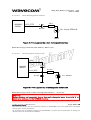
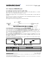
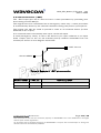
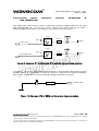
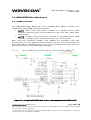
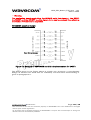
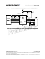
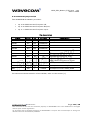
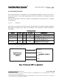
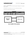
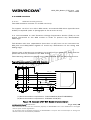
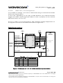
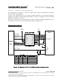
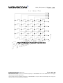
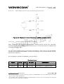
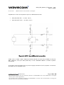
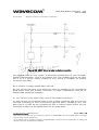
1
WISMO Quik Q25 series
WISMO Quik Q2501
Customer Design Guidelines
Reference : WM_PRJ_Q2501_PTS_002
Revision : 001
Date : March 2004
confidential ©
Page :
1 / 79
This document is the sole and exclusive property of WAVECOM. Not to be distributed or divulged
without prior written agreement.
Ce document est la propriété exclusive de WAVECOM. Il ne peut être communiqué ou divulgué à
des tiers sans son autorisation préalable.
WM_PRJ_Q2501_PTS_002 - 001
March 2004
Document Information
Revision
001
Date
History of the evolution
March 04
Preliminary version
confidential ©
Page: 2 / 79
This document is the sole and exclusive property of WAVECOM. Not to be distributed or divulged
without prior written agreement.
Ce document est la propriété exclusive de WAVECOM. Il ne peut être communiqué ou divulgué à
des tiers sans son autorisation préalable.
WM_PRJ_Q2501_PTS_002 - 001
March 2004
Overview
The WISMO Quik Q2501 module is an E-GSM/DCS - GPRS 900/1800 MHz dual
band module with 16 channels GPS receiver. It is dedicated to automotive
applications, driven by AT commands.
The WISMO Quik Q2501 memory configuration is:
GSM/GPRS part: 32 Mbits of Flash memory and 4 Mbits of SRAM,
GPS part: 8 Mbits of Flash memory.
This document gives recommendations and general guidelines to design an
application using the WISMO Quik Q2501 module.
It gives some recommendations for:
Base Band design rules and typical implementation examples,
RF design rules and typical implementation examples,
Mechanical constraints for module fitting,
PCB routing recommendations,
Test and download recommendations.
It also recommends some manufacturers and suppliers for the peripheral
devices which can be used with the WISMO Quik Q2501 modules.
For further information about the WISMO Quik Q2501 module, refer to the
Product Technical Specification (document [2]).
confidential ©
Page: 3 / 79
This document is the sole and exclusive property of WAVECOM. Not to be distributed or divulged
without prior written agreement.
Ce document est la propriété exclusive de WAVECOM. Il ne peut être communiqué ou divulgué à
des tiers sans son autorisation préalable.
WM_PRJ_Q2501_PTS_002 - 001
March 2004
Contents
Document Information......................................................................... 2
Overview ............................................................................................. 3
Contents.............................................................................................. 4
Table of figures ................................................................................... 6
Cautions .............................................................................................. 8
Trademarks ......................................................................................... 8
1
References .................................................................................... 9
1.1
Reference Documents .............................................................................9
1.2
Glossary ..................................................................................................9
1.3
Abbreviations ........................................................................................10
2
General Information .................................................................... 14
2.1
Features ................................................................................................14
2.2
Functional architecture ..........................................................................16
3
Functional Design ....................................................................... 17
3.1
Power supply part .................................................................................17
3.1.1
Main power supply and ground plane ...........................................17
3.1.2
RTC Back-up supply ......................................................................20
3.2
Common GSM/GPS part ........................................................................22
3.2.1
Module activation function (ON/~OFF)...........................................22
3.2.2
Alternative download control function (BOOT)...............................22
3.2.3
Reset function (~RST)....................................................................23
3.2.4
Activity status indication function (FLASH_LED & GPS_TIMEPULSE)24
3.3
GSM/GPRS Base Band part ...................................................................25
3.3.1
GSM serial links.............................................................................25
3.3.2
General purpose I/O .......................................................................28
3.3.3
Peripheral buses ............................................................................29
3.3.4
SIM interface .................................................................................31
3.3.5
Keyboard interface .........................................................................35
3.3.6
Audio interface ..............................................................................37
3.3.7
Buzzer interface .............................................................................43
3.3.8
Digital Power Supply for External Devices (VCC)............................44
3.3.9
GSM transmission activity status ..................................................44
3.3.10 GSM Base Band Activation indicator .............................................45
3.3.11 External Interrupt...........................................................................45
3.3.12 Auxiliary Analog Signals ................................................................46
3.4
GPS Base Band part ..............................................................................47
3.4.1
GPS activation function .................................................................47
Page: 4 / 79
confidential ©
This document is the sole and exclusive property of WAVECOM. Not to be distributed or divulged
without prior written agreement.
Ce document est la propriété exclusive de WAVECOM. Il ne peut être communiqué ou divulgué à
des tiers sans son autorisation préalable.
WM_PRJ_Q2501_PTS_002 - 001
March 2004
3.4.2
3.4.3
3.4.4
3.4.5
3.4.6
GPS serial links ..............................................................................48
Dead reckoning interface ...............................................................50
1.8 V Digital Power Supply for External Devices ............................52
GPS External Interruption ..............................................................52
GPS Antenna Power Supply ..........................................................52
3.5
RF part ..................................................................................................53
3.5.1
Antenna connection possibilities ...................................................53
3.5.2
GSM/GPRS antenna connection.....................................................54
3.5.3
GPS antenna connection ...............................................................55
3.5.4
Single coax connection ..................................................................59
4
4.1
PCB Design ................................................................................. 60
General Rules and Constraints ..............................................................60
4.2
Specific Routing Constraints .................................................................60
4.2.1
System Connector .........................................................................60
4.2.2
Power Supply ................................................................................60
4.2.3
SIM interface routing constraints...................................................62
4.2.4
Audio circuit routing constraints....................................................62
4.2.5
RF circuit routing constraints.........................................................63
4.3
Pads design...........................................................................................67
5
Mechanical Specifications .......................................................... 68
6
EMC and ESD recommendations................................................. 70
7
Firmware upgrade requirements ................................................. 71
8
Embedded Testability.................................................................. 72
8.1
Access to the serial link .........................................................................72
8.2
RF output accessibility for diagnostic ....................................................74
9
Manufacturers and suppliers ...................................................... 75
9.1
System connector .................................................................................75
9.2
SIM Card Reader ...................................................................................75
9.3
Microphone ...........................................................................................75
9.4
Speaker .................................................................................................76
9.5
RF cable ................................................................................................76
9.6
GSM antenna ........................................................................................76
9.7
GPS antenna .........................................................................................77
9.8
Buzzer ...................................................................................................77
10
Appendix .................................................................................. 78
10.1
80-pin PCB receptacle ...........................................................................79
confidential ©
Page: 5 / 79
This document is the sole and exclusive property of WAVECOM. Not to be distributed or divulged
without prior written agreement.
Ce document est la propriété exclusive de WAVECOM. Il ne peut être communiqué ou divulgué à
des tiers sans son autorisation préalable.
WM_PRJ_Q2501_PTS_002 - 001
March 2004
Table of figures
Figure 1: Functional architecture .................................................................... 16
Figure 2: Typical Power supply voltage in GSM/GPRS mode .......................... 18
Figure 3: RTC supplied by a super capacitor................................................... 20
Figure 4: RTC supplied by a non rechargeable battery.................................... 21
Figure 5: RTC supplied by a rechargeable battery cell .................................... 21
Figure 6: Example of ON/~OFF pin connection ............................................... 22
Figure 7: Example of BOOT pin connection .................................................... 22
Figure 8: Example of ~RST pin connection ..................................................... 23
Figure 9: Example N°1 of GSM and GPS activity status implementation ......... 24
Figure 10: Example N°2 of GSM activity status implementation ..................... 24
Figure 11: Example of RS232 level shifter implementation for GSM UART1 ... 25
Figure 12: Example of V24/CMOS serial link implementation for UART1 ........ 26
Figure 13: Example of RS232 level shifter implementation for GSM UART2 ... 27
Figure 14: Example of SPI bus application...................................................... 29
Figure 15: example of 2 wire bus application ................................................. 30
Figure 16: Example of 3V SIM Socket implementation.................................... 31
Figure 17: Example of 1.8 V / 3 V SIM interface implementation .................... 33
Figure 18: Example of 3 V / 5 V SIM interface implementation ....................... 34
Figure 19: Example of keyboard implementation ............................................ 36
Figure 20: Example of main microphone (MIC2) implementation.................... 38
Figure 21: MIC1 input differential connection ................................................. 39
Figure 22: MIC1 input single ended connection ............................................. 40
Figure 23: Speaker differential connection ...................................................... 41
Figure 24: Speaker single-ended connection .................................................. 42
confidential ©
Page: 6 / 79
This document is the sole and exclusive property of WAVECOM. Not to be distributed or divulged
without prior written agreement.
Ce document est la propriété exclusive de WAVECOM. Il ne peut être communiqué ou divulgué à
des tiers sans son autorisation préalable.
WM_PRJ_Q2501_PTS_002 - 001
March 2004
Figure 25: Example of buzzer implementation ................................................ 43
Figure 26: LED driven by the BUZ output ....................................................... 43
Figure 27: ~INTR driving example .................................................................. 45
Figure 28: Example of ADC application........................................................... 46
Figure 29: GPS activation function implementation ........................................ 47
Figure 30: Example of RS232 level shifter implementation for GPS UART2 .... 48
Figure 31: Example of RS232 level shifter implementation for GPS UART0 .... 49
Figure 32: SPI interface implementation for the dead reckoning function ....... 50
Figure 33: Block diagram of the GPS antenna connection .............................. 55
Figure 34: GPS reception jammed by GSM/GPRS transmission ...................... 57
Figure 35: Example of Q2501 module and GPS antenna integrated application
...................................................................................................................... 58
Figure 36 :Example of power supply routing .................................................. 60
Figure 37: Burst simulation circuit.................................................................. 61
Figure 38: AppCad Screenshot for MicroStrip design ..................................... 63
Figure 39: Example of PCB routing for pigtail connection ............................... 66
Figure 40: Pads design................................................................................... 67
Figure 41: GSM UART1 serial link debug access ............................................ 72
Figure 42: Module connection for RF measurements...................................... 74
confidential ©
Page: 7 / 79
This document is the sole and exclusive property of WAVECOM. Not to be distributed or divulged
without prior written agreement.
Ce document est la propriété exclusive de WAVECOM. Il ne peut être communiqué ou divulgué à
des tiers sans son autorisation préalable.
WM_PRJ_Q2501_PTS_002 - 001
March 2004
Cautions
Information furnished herein by Wavecom are accurate and reliable. However
no responsibility is assumed for its use. Please read carefully the safety
precautions for an application based on a WISMO Quik Q2501 module.
In addition, Wavecom reserves the right to modify this information with an aim
of improving the accuracy of information provided herein.
General information about Wavecom and its range of products is available at
the following internet address: http://www.wavecom.com
Trademarks
WAVECOM and WISMO are trademarks or registered trademarks of Wavecom
S.A. All other company and/or product names mentioned may be trademarks or
registered trademarks of their respective owners.
confidential ©
Page: 8 / 79
This document is the sole and exclusive property of WAVECOM. Not to be distributed or divulged
without prior written agreement.
Ce document est la propriété exclusive de WAVECOM. Il ne peut être communiqué ou divulgué à
des tiers sans son autorisation préalable.
WM_PRJ_Q2501_PTS_002 - 001
March 2004
1 References
1.1 Reference Documents
[1]
Automotive Environmental Control Plan for WISMO Quik Q2501
WM_PRJ_Q2501_DCP_001
[2]
WISMO Quik Q2501 Product Technical Specification
WM_PRJ_Q2501_PTS_001
[3]
WISMO Quik Q2501 Process Customer Guidelines
WM_PRJ_Q2501_PTS_003
1.2 Glossary
Term
Definition
Performing a FIX
Means the GPS receiver is able to compute a
position
Dead reckoning
GPS Feature that allows navigation with poor/no
satellites view by the aid of external sensors that
provide
course
(odometer)
and
heading
(gyroscope).
Single Coax
WAVECOM concept that allows the user to use
only one single coaxial cable for both GSM and
GPS RF signal to connect the WISMO Quik Q2501
module to the antennas.
The antennas are most of the time physically
distinct but connected to the WISMO Quik Q2501
module by a single coaxial cable through an
antenna switch system, saving a second coaxial
cable.
Cold Start
Powering up a unit after it has been turned off for
an extended period of time and no longer contains
current ephemeris data. In Cold Start Scenario, the
receiver has no knowledge on last position,
approximate time or satellite constellation. The
receiver starts to search for signals blindly. This is
normal behavior, if no backup battery is connected.
Cold Start time is the longest startup time for GPS
receivers and can be several minutes.
confidential ©
Page: 9 / 79
This document is the sole and exclusive property of WAVECOM. Not to be distributed or divulged
without prior written agreement.
Ce document est la propriété exclusive de WAVECOM. Il ne peut être communiqué ou divulgué à
des tiers sans son autorisation préalable.
WM_PRJ_Q2501_PTS_002 - 001
March 2004
Term
Definition
Hot Start
Start mode of the GPS receiver when current
position, clock offset, approximate GPS time and
current ephemeris data are all available. In Hot
Start Scenario, the receiver was off for less than
2 hours. It uses its last Ephemeris data to calculate
a position fix.
Warm Start
Start mode of a GPS receiver when current
position, clock offset and approximate GPS time are
known. Almanac data is retained, but the
ephemeris data is cleared. In Warm Start Scenario,
the receiver knows - due to a backup battery or by
other techniques – his last position,
approximate time and almanac. Thanks to this, it
can quickly acquire satellites and get a
position fix faster than in cold start mode.
Coarse Acquisition
Code (C/A Code)
The standard positioning signal the GPS satellite
transmits to the civilian user. It contains the
information the GPS receiver uses to fix its position
and time. Accurate to 24 meter. This code is a
sequence of 1023 pseudorandom binary biphase
modulations on the GPS carrier (L1) at a chipping
rate of 1.023 MHz, thus having a code repetition
period of 1 millisecond. The code was selected to
provide good acquisition properties. Also known as
the "civilian code.".
1.3 Abbreviations
Abbreviation Definition
AC
Alternative Current
ADC
Analogue to Digital Converter
A/D
Analogue to Digital conversion
AF
Audio-Frequency
AT
ATtention (prefix for modem commands)
AUX
AUXiliary
CAN
Controller Area Network
CB
Cell Broadcast
CEP
Circular Error Probable
CLK
CLocK
confidential ©
Page: 10 / 79
This document is the sole and exclusive property of WAVECOM. Not to be distributed or divulged
without prior written agreement.
Ce document est la propriété exclusive de WAVECOM. Il ne peut être communiqué ou divulgué à
des tiers sans son autorisation préalable.
WM_PRJ_Q2501_PTS_002 - 001
March 2004
Abbreviation Definition
CMOS
Complementary Metal Oxide Semiconductor
CS
Coding Scheme
CTS
Clear To Send
DAC
Digital to Analogue Converter
dB
Decibel
DC
Direct Current
DCD
Data Carrier Detect
DCE
Data Communication Equipment
DCS
Digital Cellular System
DR
Dynamic Range
DSR
Data Set Ready
DTE
Data Terminal Equipment
DTR
Data Terminal Ready
EFR
Enhanced Full Rate
E-GSM
Extended GSM
EMC
ElectroMagnetic Compatibility
EMI
ElectroMagnetic Interference
EMS
Enhanced Message Service
EN
ENable
ESD
ElectroStatic Discharges
FIFO
First In First Out
FR
Full Rate
FTA
Full Type Approval
GND
GrouND
GPI
General Purpose Input
GPIO
General Purpose Input Output
GPO
General Purpose Output
GPRS
General Packet Radio Service
GPS
Global Positioning System
GSM
Global System for Mobile communications
HR
Half Rate
I/O
Input / Output
LED
Light Emitting Diode
LNA
Low Noise Amplifier
confidential ©
Page: 11 / 79
This document is the sole and exclusive property of WAVECOM. Not to be distributed or divulged
without prior written agreement.
Ce document est la propriété exclusive de WAVECOM. Il ne peut être communiqué ou divulgué à
des tiers sans son autorisation préalable.
WM_PRJ_Q2501_PTS_002 - 001
March 2004
Abbreviation Definition
MAX
MAXimum
MIC
MICrophone
MIN
MINimum
MMS
Multimedia Message Service
MO
Mobile Originated
MT
Mobile Terminated
NF
Noise Factor
NMEA
National Marine Electronics Association
NOM
NOMinal
PA
Power Amplifier
Pa
Pascal (for speaker sound pressure measurements)
PBCCH
Packet Broadcast Control CHannel
PC
Personal Computer
PCB
Printed Circuit Board
PDA
Personal Digital Assistant
PFM
Power Frequency Modulation
PSM
Phase Shift Modulation
PWM
Pulse Width Modulation
RAM
Random Access Memory
RF
Radio Frequency
RFI
Radio Frequency Interference
RHCP
Right Hand Circular Polarization
RI
Ring Indicator
RST
ReSeT
RTC
Real Time Clock
RTCM
Radio Technical Commission for Maritime services
RTS
Request To Send
RX
Receive
SIM
Subscriber Identification Module
SMS
Short Message Service
SPI
Serial Peripheral Interface
SPL
Sound Pressure Level
SPK
SPeaKer
SRAM
Static RAM
confidential ©
Page: 12 / 79
This document is the sole and exclusive property of WAVECOM. Not to be distributed or divulged
without prior written agreement.
Ce document est la propriété exclusive de WAVECOM. Il ne peut être communiqué ou divulgué à
des tiers sans son autorisation préalable.
WM_PRJ_Q2501_PTS_002 - 001
March 2004
Abbreviation Definition
TBC
To Be Confirmed
TDMA
Time Division Multiple Access
TP
Test Point
TVS
Transient Voltage Suppressor
TX
Transmit
TYP
TYPical
UART
Universal Asynchronous Receiver-Transmitter
USB
Universal Serial Bus
USSD
Unstructured Supplementary Services Data
VSWR
Voltage Stationary Wave Ratio
confidential ©
Page: 13 / 79
This document is the sole and exclusive property of WAVECOM. Not to be distributed or divulged
without prior written agreement.
Ce document est la propriété exclusive de WAVECOM. Il ne peut être communiqué ou divulgué à
des tiers sans son autorisation préalable.
WM_PRJ_Q2501_PTS_002 - 001
March 2004
2 General Information
2.1 Features
WISMO Quik Q2501 is self-contained E-GSM/DCS-GPRS 900/1800 dual-band
module with 16 bits GPS receiver.
Following table reminds the WISMO Quik Q2501 features:
Feature
Information
Physical
characteristics
Size: 58.4 x 32.2 x 6.3 mm.
Weight: 11 g.
Complete shielding.
Module control
Full set of AT commands for GSM/GPRS including
GSM 07.07 and 07.05 AT command sets.
Specific AT commands for GPS management on same
link as GSM/GPRS AT commands.
Direct reception of GPS data through serial link.
Status indication for GSM and for GPS functions.
GSM/DCS
Frequency bands:
•
Rx (E-GSM 900): 925 to 960 MHz.
•
Rx (DCS 1800): 1805 to 1880 MHz.
•
Tx (E-GSM 900): 880 to 915 MHz.
• Tx (DCS 1800): 1710 to 1785 MHz.
Transmit power:
•
Class 4 (2 W) at E-GSM
•
Class 1 (1 W) at DCS
GPRS
GPRS multislot class 10.
Multislot class 2 supported.
PBCCH support.
Coding schemes: CS1 to CS4.
Voice Features
GSM Voice Features with Emergency calls 112.
Full Rate (FR)/ Enhanced Full Rate (EFR) / Half Rate
(HR).
Echo cancellation and noise reduction.
Full duplex Hands free.
SMS
SMS MT, MO and SMS CB
SMS storage into SIM card
confidential ©
Page: 14 / 79
This document is the sole and exclusive property of WAVECOM. Not to be distributed or divulged
without prior written agreement.
Ce document est la propriété exclusive de WAVECOM. Il ne peut être communiqué ou divulgué à
des tiers sans son autorisation préalable.
WM_PRJ_Q2501_PTS_002 - 001
March 2004
Feature
Information
GSM Supplementary
Services
Call Forwarding, Call Barring.
Multiparty.
Call Waiting, Call Hold.
USSD.
Data / Fax
Data circuit asynchronous, transparent, and nontransparent up to 14400 bits/s.
Fax Group 3 compatible.
SIM interface
3 V only SIM interface.
1.8 & 5 V SIM interfaces are available with external
adaptation.
SIM Tool Kit Release 99.
GPS
GPS L1 civil frequency 1575.42 MHz.
16 channels GPS receiver.
Accuracy:
•
2.5 m CEP.
•
GPS 2 m CEP (depending on accuracy of
correction data); SBAS/WAAS supported.
Start-up times :
•
Hot start: < 3.5 sec.
•
Warm start: 33 sec.
• Cold start: 34 sec.
Signal reacquisition < 1 s.
Protocols:
•
NMEA-0183 input/output.
•
UBX binary input/output.
• RTCM in.
Interface available for Dead Reckoning.
Real Time Clock
Real Time Clock with calendar and alarm.
RTC update with GPS information.
Temperature sensor
Internal sensor for module temperature monitoring via
AT commands or embedded OpenAT application.
Advanced
antennas Single Coax connectivity.
management
GPS active antenna management (3 V / 5 V
compatible) with internal protection circuit.
Possible use of an auto-powered GPS active antenna.
confidential ©
Page: 15 / 79
This document is the sole and exclusive property of WAVECOM. Not to be distributed or divulged
without prior written agreement.
Ce document est la propriété exclusive de WAVECOM. Il ne peut être communiqué ou divulgué à
des tiers sans son autorisation préalable.
WM_PRJ_Q2501_PTS_002 - 001
March 2004
2.2 Functional architecture
POWER SUPPLY INTERFACE
RF GSM
FRONT END
W
I
S
M
O
GSM / GPRS
Audio filter
Q
2
5
0
1
BASEBAND
GSM / GPS
ANTENNA
ANTENNAS
S
Y
S
T
E
M
C
N
N
E
C
T
O
R
CONTROL
GPS
ANTENNA
GSM Flash memory
GPS
BASEBAND
RF PORTS
RF GPS
FRONT END
GPS Flash memory
Figure 1: Functional architecture
confidential ©
Page: 16 / 79
This document is the sole and exclusive property of WAVECOM. Not to be distributed or divulged
without prior written agreement.
Ce document est la propriété exclusive de WAVECOM. Il ne peut être communiqué ou divulgué à
des tiers sans son autorisation préalable.
WM_PRJ_Q2501_PTS_002 - 001
March 2004
3 Functional Design
Some of the WISMO interface signals are multiplexed in order to limit the
number of pins but this architecture implies some restrictions.
All external signals must be inactive when the WISMO module is OFF to avoid
any damage when starting the module.
3.1 Power supply part
3.1.1 Main power supply and ground plane
3.1.1.1
Electrical constraints
The main power supply (VBATT) is the only external power supply source used
to supply both the GSM/GPRS and GPS RF parts and Base Band parts.
The power supply is one of the key issues in the design of a GSM terminal.
Due to the bursted emission in GSM / GPRS, the power supply must be able to
deliver high current peaks in a short time (rising time is around 10 µs).
In communication mode, the GSM RF Power Amplifier current flows with a
ratio of (Figure 2):
•
Max current 1/8 of the time (around 577 µs every 4.615 ms for
GSM/GPRS class 2 – 2RX / 1TX),
•
Max current 2/8 of the time (around 1154 µs every 4.615 ms for
GSM/GPRS class 10 – 3RX / 2TX).
confidential ©
Page: 17 / 79
This document is the sole and exclusive property of WAVECOM. Not to be distributed or divulged
without prior written agreement.
Ce document est la propriété exclusive de WAVECOM. Il ne peut être communiqué ou divulgué à
des tiers sans son autorisation préalable.
WM_PRJ_Q2501_PTS_002 - 001
March 2004
Vmax
VBATT
Uripp
Uripp
Vmin
IBATT
T=577µs
T = 4.615ms
Legend:
In GSM or GPRS class 2 modes
In GPRS class 10 mode
Figure 2: Typical Power supply voltage in GSM/GPRS mode
During these peaks the ripple (Uripp) on the supply voltage must not exceed a
certain limit (refer to document [2]).
Because VBATT supplies directly the GSM RF power amplifier component, it is
essential to keep a minimum voltage ripple at this connection in order to avoid
any phase error or spectrum modulation degradation.
On the other hand, insufficient power supply voltage could dramatically affect
some RF performances: TX power, modulation spectrum, EMC (ElectroMagnetic Compatibility) performances, spurious emission and frequency error.
The power supply voltage features given in the table hereunder will guarantee
nominal functioning of the module.
Power Supply Voltage
VBATT
VMIN
VNOM
VMAX
Uripp max
3.4 V (*)
3.6 V
4.5 V (**)
50 mVpp for freq<200 kHz
5 mVpp for freq>200 kHz
(*): This value has to be guaranteed during the burst (with 2.0 A Peak in GSM
or GPRS mode).
(**): max operating Voltage Stationary Wave Ratio (VSWR) 2:1.
confidential ©
Page: 18 / 79
This document is the sole and exclusive property of WAVECOM. Not to be distributed or divulged
without prior written agreement.
Ce document est la propriété exclusive de WAVECOM. Il ne peut être communiqué ou divulgué à
des tiers sans son autorisation préalable.
WM_PRJ_Q2501_PTS_002 - 001
March 2004
3.1.1.2
Design requirements
A Careful attention should be paid to:
Quality of the power supply:
o
linear regulation (recommended) or PWM (Pulse
Modulation) converter (usable) are preferred for low noise.
o
PFM (Power Frequency modulation)
Modulation) systems must be avoided.
or
PSM
(Phase
Width
Shift
Capacity to deliver high current peaks in a short time (bursted radio
emission).
The VBATT line must support peak currents with an acceptable voltage
drop which guarantees a VBATT minimal value of 3.4 V (lower limit of
VBATT).
For PCB design constraints related to power supply tracks, ground planes and
shielding, refer to paragraph 4.2.2.
3.1.1.3
Decoupling of power supply signals
Decoupling capacitors on VBATT lines are imbedded in the module. So it
should not be necessary to add decoupling capacitors close to the module.
However, in case of EMI/RFI problem, VBATT signal may require some EMI/RFI
decoupling: parallel 33 pF capacitor close to the module or a serial ferrite bead
(or both to get better results).
In case a ferrite bead is used, the recommendation given for the power supply
connection must be carefully followed (high current capacity and low
impedance).
confidential ©
Page: 19 / 79
This document is the sole and exclusive property of WAVECOM. Not to be distributed or divulged
without prior written agreement.
Ce document est la propriété exclusive de WAVECOM. Il ne peut être communiqué ou divulgué à
des tiers sans son autorisation préalable.
WM_PRJ_Q2501_PTS_002 - 001
March 2004
3.1.2 RTC Back-up supply
3.1.2.1
Design requirements
VCC_RTC pin is used to provide a back-up power supply for the internal Real
Time Clock (RTC).
The RTC is supported by the WISMO Quik Q2501 module when powered on,
but a back-up power supply is needed to save date and time information
when the module is switched off.
If the RTC is not used this pin can be left open.
Back-up Power Supply can be provided by:
A super capacitor,
A non rechargeable battery,
A rechargeable battery cell.
3.1.2.2
3.1.2.2.1
Typical application electrical diagram
Super Capacitor
WISMO
Q2501
VCC_RTC
470 Ω
+
Ex: EECEOEL474S
(Panasonic)
GND
Figure 3: RTC supplied by a super capacitor
Estimated range with 0.47 Farad Gold Cap: 25 minutes min.
Note: the Gold Capacitor maximum voltage is 2.5 V.
confidential ©
Page: 20 / 79
This document is the sole and exclusive property of WAVECOM. Not to be distributed or divulged
without prior written agreement.
Ce document est la propriété exclusive de WAVECOM. Il ne peut être communiqué ou divulgué à
des tiers sans son autorisation préalable.
WM_PRJ_Q2501_PTS_002 - 001
March 2004
3.1.2.2.2
WISMO
Q2501
Non Rechargeable battery
VCC_RTC
1
3
10 Ω
BAS16
Ex: Varta CR2016
GND
Figure 4: RTC supplied by a non rechargeable battery
Estimated range with 85 mAh battery: 800 h min.
3.1.2.2.3
Rechargeable battery cell
3
WISMO
Q2501
BAS40
1
VCC
2.2 kΩ
VCC_RTC
Ex: ML621
2.2 µF
GND
GND
Figure 5: RTC supplied by a rechargeable battery cell
Estimated range with 2 mAh rechargeable battery: ~15 hours.
Warning:
Before battery cell assembly insure that cell voltage is lower than 2.75 V to
avoid any damage to the WISMO module.
confidential ©
Page: 21 / 79
This document is the sole and exclusive property of WAVECOM. Not to be distributed or divulged
without prior written agreement.
Ce document est la propriété exclusive de WAVECOM. Il ne peut être communiqué ou divulgué à
des tiers sans son autorisation préalable.
WM_PRJ_Q2501_PTS_002 - 001
March 2004
3.2 Common GSM/GPS part
3.2.1 Module activation function (ON/~OFF)
The ON/~OFF input (pin 26) is used to switch ON (ON/~OFF=1) or OFF
(ON/~OFF=0) the WISMO Quik Q2501 module.
A high level signal has to be provided on the pin ON/~OFF to swith ON the
module.
The level of the voltage of this signal has to be maintained between 2.4 V and
VBATT during a minimum of 500 ms.
This signal can be left at high level until switch OFF.
SW500
1
2
VBATT
ON/~OFF
3
Figure 6: Example of ON/~OFF pin connection
3.2.2 Alternative download control function (BOOT)
If the standard X-modem download procedure does not work correctly, an
alternative download procedure can be selected with the BOOT input (pin 32).
This alternative download procedure requires a specific downloading software
tool.
The alternative download procedure is started when the BOOT pin is low
during the reset of the module. A low level of BOOT input has to be set
through a 1 kΩ resistor.
If used, this input has to be driven by an open collector or an open drain output
as shown in the diagram hereunder:
1 kΩ
BOOT pin
Switch BOOT
1 kΩ
OR
BOOT pin
Switch BOOT
Figure 7: Example of BOOT pin connection
Switch BOOT
BOOT pin
1
0
Alternative download mode (use of BOOT input)
0
1
Normal download mode (use of X-modem protocol)
confidential ©
Operating mode
Page: 22 / 79
This document is the sole and exclusive property of WAVECOM. Not to be distributed or divulged
without prior written agreement.
Ce document est la propriété exclusive de WAVECOM. Il ne peut être communiqué ou divulgué à
des tiers sans son autorisation préalable.
WM_PRJ_Q2501_PTS_002 - 001
March 2004
3.2.3 Reset function (~RST)
The ~RST input (pin 34) is used to force a reset procedure by providing low
level during at least 500 µs.
This signal has to be considered as an emergency reset only: a reset procedure
is automatically driven by an internal hardware during the power-up sequence.
This signal can also be used to provide a reset to an external device (it then
behaves as an output).
If no external reset is necessary this input can be left open.
If used (emergency reset), it has to be driven by an open collector or an open
drain output (due to the 4.7 kΩ internal pull-up resistor embedded into the
module) as shown in the diagram hereunder.
~RST: Pin 34
Switch RESET
Figure 8: Example of ~RST pin connection
Switch RESET
~RST pin
1
0
Reset activated
0
1
Reset inactive
confidential ©
Operating mode
Page: 23 / 79
This document is the sole and exclusive property of WAVECOM. Not to be distributed or divulged
without prior written agreement.
Ce document est la propriété exclusive de WAVECOM. Il ne peut être communiqué ou divulgué à
des tiers sans son autorisation préalable.
WM_PRJ_Q2501_PTS_002 - 001
March 2004
3.2.4 Activity
status
GPS_TIMEPULSE)
indication
function
(FLASH_LED
&
The GSM and GPS activity status indication signals (FLASH_LED pin 72 and
GPS_TIMEPULSE pin 17) can be used to drive two LEDs through an opencollector digital transistor according to the module activity status.
« GSM »
U700
GND
FLASH_LED
1
6
2
R700
470 Ω
U700
GND
GPS_TIMEPULSE
4
2
1
VBATT
D700
« GPS »
3
5
R702
470 Ω
2
1
VBATT
D702
Figure 9: Example N°1 of GSM and GPS activity status implementation
In addition, given the electrical characteristics of the FLASH_LED output signal
(CMOS 2.8 V), it is possible to directly connect a LED and a resistor between
this output and VBATT to avoid adding a digital transistor inverter.
2
1
470 Ω
FLASH_LED
GND
Figure 10: Example N°2 of GSM activity status implementation
confidential ©
Page: 24 / 79
This document is the sole and exclusive property of WAVECOM. Not to be distributed or divulged
without prior written agreement.
Ce document est la propriété exclusive de WAVECOM. Il ne peut être communiqué ou divulgué à
des tiers sans son autorisation préalable.
WM_PRJ_Q2501_PTS_002 - 001
March 2004
3.3 GSM/GPRS Base Band part
3.3.1 GSM serial links
The GSM/GPRS Base Band part of the WISMO Quik Q2501 includes two
independent V24/CMOS serial link interfaces:
UART1 (main serial link) which consists in a flexible 8-wire serial
interface complying with V24 standard (TX, RX, CTS, RTS, DSR, DTR,
DCD and RI),
UART2 (auxiliary serial link) which consists in a flexible 4-wire serial
interface complying with V24 standard (TX, RX, CTS and RTS).
Both serial link interfaces (UART1 and UART2) are compliant with V24
standard but not with V28 (electrical interface) due to a 2.8 Volt interface. To
get a V24/V28 (i.e. RS232) interface, the use of an RS232 level shifter device is
required as shown in the following paragraphs.
3.3.1.1
Main GSM Serial Link implementation (GSM_UART1)
Figure 11: Example of RS232 level shifter implementation for GSM UART1
confidential ©
Page: 25 / 79
This document is the sole and exclusive property of WAVECOM. Not to be distributed or divulged
without prior written agreement.
Ce document est la propriété exclusive de WAVECOM. Il ne peut être communiqué ou divulgué à
des tiers sans son autorisation préalable.
WM_PRJ_Q2501_PTS_002 - 001
March 2004
Warning:
The application board must allow the WISMO serial link signals + the BOOT,
the RESET and the ON/OFF module signals to be easily accessed thus allowing
the module firmware to be upgraded.
V24/CMOS possible design:
Host Microprocessor
Figure 12: Example of V24/CMOS serial link implementation for UART1
The design given in the Figure above is a basic one. However, a more flexible
design to access this serial link for testability and firmware downloading is
given in paragraph 8.1.
confidential ©
Page: 26 / 79
This document is the sole and exclusive property of WAVECOM. Not to be distributed or divulged
without prior written agreement.
Ce document est la propriété exclusive de WAVECOM. Il ne peut être communiqué ou divulgué à
des tiers sans son autorisation préalable.
WM_PRJ_Q2501_PTS_002 - 001
March 2004
3.3.1.2
Auxiliary GSM Serial Link implementation (GSM_UART2)
GND
1
C204
100 nF
2
C200
470 nF
C0805
1
2
C201
470 nF
C0805
3V3
16
1
2
1
C203
470 nF
C0805
2
C202
470 nF
C0805
1
3
4
5
WISMO
GSM_CTS2
GSM_RXD2
Q2501
11
10
GSM_RTS2
12
GSM_TXD2
9
VCC
C1+
C1C2+
C2-
V+
3232
U200
SSOP16
V-
T1IN
T1OUT
T2IN
T2OUT
R1OUT
R1IN
R2OUT
R2IN
GND
15
2
J200
SUB-D9F-C
6
14
S_CTS2
7
S_RXD2
13
S_RTS2
8
S_TXD2
8
2
6
NC
GND
9
1
5
7
4
3
GND
Figure 13: Example of RS232 level shifter implementation for GSM UART2
confidential ©
Page: 27 / 79
This document is the sole and exclusive property of WAVECOM. Not to be distributed or divulged
without prior written agreement.
Ce document est la propriété exclusive de WAVECOM. Il ne peut être communiqué ou divulgué à
des tiers sans son autorisation préalable.
WM_PRJ_Q2501_PTS_002 - 001
March 2004
3.3.2 General purpose I/O
The WISMO Quik Q2501 provides:
up to 6 GSM General Purpose I/O,
up to 4 GSM General Purpose Output,
up to 1 GSM General Purpose Input.
Pin description
Signal
Pin #
I/O
I/O type
Description
GPIO0
44
I/O
CMOS3X
GPIO1
22
I/O
CMOS/2X
GPIO2
24
I/O
CMOS/2X
GPIO3
53
I/O
CMOS/2X
GPIO4
73
I/O
CMOS/2X
GPIO5
55
I/O
CMOS/3X
GPO0
46
O
3X
Multiplexed with SPI_AUX
GPO1
42
O
3X
Multiplexed with 1V8/3V or 3V/5V
SIM card management signal
GPO2
40
O
3X
Multiplexed with GSM_RXD2
GPO3
48
O
3X
Multiplexed with SPI_EN
GPI
38
I
CMOS
Multiplexed with GSM_CTS2
Multiplexed with GSM_RTS2
Multiplexed with GSM_TXD2
For electrical characteristics of the GPIOs, refer to document [1].
confidential ©
Page: 28 / 79
This document is the sole and exclusive property of WAVECOM. Not to be distributed or divulged
without prior written agreement.
Ce document est la propriété exclusive de WAVECOM. Il ne peut être communiqué ou divulgué à
des tiers sans son autorisation préalable.
WM_PRJ_Q2501_PTS_002 - 001
March 2004
3.3.3 Peripheral buses
One peripheral bus is available on the WISMO Quik Q2501 System Connector.
It can be used to drive SPI peripherals (3-wire interface) or standard 2-wire
peripherals.
The choice between these two types of peripherals is exclusive due to signal
multiplexing.
3.3.3.1
SPI Bus
The SPI bus includes clock (SPI_CLK), I/O (SPI_IO) and enable signals (SPI_EN,
SPI_AUX) complying with SPI bus standard. The maximum speed transfer is
3.25 Mb/s.
Pin description
Signal
Pin #
I/O
I/O type
Description
SDA/SPI_IO
28
I/O
CMOS/3X
SCL/SPI_CLK
30
O
3X
SPI clock
SPI_EN
48
O
3X
Main SPI enable signal
Multiplexed with GPO3
SPI_AUX
46
O
3X
Auxiliary SPI enable signal
Multiplexed with GPO0
SPI data signal
SDA/SPI_IO
Application
processor
(DTE)
SCL/SPI_CLK
WISMO Q2501
SPI_AUX
SPI_EN
Figure 14: Example of SPI bus application
confidential ©
Page: 29 / 79
This document is the sole and exclusive property of WAVECOM. Not to be distributed or divulged
without prior written agreement.
Ce document est la propriété exclusive de WAVECOM. Il ne peut être communiqué ou divulgué à
des tiers sans son autorisation préalable.
WM_PRJ_Q2501_PTS_002 - 001
March 2004
3.3.3.2
Two-wire bus
The 2-wire interface includes clock and data signals complying with a standard
96 kHz interface.
Each signal has to be pulled-up to VCC via an external 2.2 kΩ resistor.
The maximum speed transfer is 400 kbits/s.
Pin description
Signal
Pin #
I/O
I/O type
Description
SCL/SPI_CLK
30
O
3X
Serial Clock
SDA/SPI_IO
28
I/O
CMOS/3X
Serial Data
SDA/SPI_IO
Application
processor
(DTE)
WISMO Q2501
SCL/SPI_CLK
Figure 15: example of 2 wire bus application
confidential ©
Page: 30 / 79
This document is the sole and exclusive property of WAVECOM. Not to be distributed or divulged
without prior written agreement.
Ce document est la propriété exclusive de WAVECOM. Il ne peut être communiqué ou divulgué à
des tiers sans son autorisation préalable.
WM_PRJ_Q2501_PTS_002 - 001
March 2004
3.3.4 SIM interface
3.3.4.1
SIM 3V management
The SIM interface controls a 3 V SIM card only.
To support 1.8 V/3 V or 3 V/5 V SIM cards, an external SIM driver (specific level
shifter) is required (refer to paragraphs 3.3.4.2 and 3.3.4.3).
It is recommended to add Transient Voltage Suppressor diodes (TVS) on the
signal connected to the SIM socket in order to prevent any ElectroStatic
Discharge.
TVS diodes with low capacitance (less than 10 pF) have to be connected on
SIM_CLK and SIM_DATA signals to avoid any disturbance of the rising and
falling edge.
These types of diodes are mandatory for the Full Type Approval. They shall be
placed as close as possible to the SIM socket.
The following references can be used: DALC208SC6 from ST Microelectronics.
Typical implementation with SIM detection:
SIM_VCC
1
SIM_RST
2 RST
VCC
SIM_CLK
3
CLK
VCC
4
CC4
5 GND
C
100 nF
GND
VPP
SIM_DATA
7
SIM_PRES
8
I/O
CC8
100
kΩ
(1)
(2)
470pf
GND
GND
GND
(1) Recommended components: DALC208SC6 (SGS-THOMSON).
(2) Recommended components: ESDA6V1SC6 (ST).
Figure 16: Example of 3V SIM Socket implementation
confidential ©
Page: 31 / 79
This document is the sole and exclusive property of WAVECOM. Not to be distributed or divulged
without prior written agreement.
Ce document est la propriété exclusive de WAVECOM. Il ne peut être communiqué ou divulgué à
des tiers sans son autorisation préalable.
WM_PRJ_Q2501_PTS_002 - 001
March 2004
SIM socket connection:
Pin description
Signal
Pin number
Description
VCC
1
SIM_VCC
RST
2
SIM_RST
CLK
3
SIM_CLK
CC4
4
VCC module
GND
5
GROUND
VPP
6
Not connected
I/O
7
SIM_DATA
CC8
8
SIM_PRES with 100 kΩ pull down resistor
The capacitor placed on the SIM_VCC line must not exceed 470 nF.
confidential ©
Page: 32 / 79
This document is the sole and exclusive property of WAVECOM. Not to be distributed or divulged
without prior written agreement.
Ce document est la propriété exclusive de WAVECOM. Il ne peut être communiqué ou divulgué à
des tiers sans son autorisation préalable.
WM_PRJ_Q2501_PTS_002 - 001
March 2004
3.3.4.2
SIM 1.8 V / 3 V management
It is possible to manage 1.8 V and 3 V SIM cards using an external level shifter
device (see Figure below).
In this case, depending on the type of SIM detected, the module firmware
triggers the GPO1 output signal (pin #42) in order to properly set the external
SIM driver level (1.8 V or 3 V).
As for 3 V SIM, it is recommended to add Transient Voltage Suppressors on
the signals connected to the SIM socket (refer to Figure 16).
Typical implementation:
VCC
2.8 V
VCC
2.8 V
LEVEL SHIFTER
4
5
WISMO
Q2501
GPO1
6
7
SIM_VCC
8
CIN
CLK
RIN
RST
DATA
I/O
DDRV
VCC
DVCC
VIN
M2
C1+
M1
C1-
M0
GND
16
3
15
2
14
7
13
1
RST
I/O
VCC = 1.8 V or 3 V
IVCC = 10 mA
12
11
10
9
VCC
LTC1555L-1.8
100 kΩ
470 pF
SIM_PRES
Truth table:
CLK
2.2 µF
VCC
2
1 µF
3
1
100 nF
SIM_CLK
SIM_RST
SIM_DATA
SIM
Socket
1Ω
to
4.7 Ω
6
VPP
4
CC4
8
CC8
5
GND
DVCC = 2.8 V
M0
M1
M2
0V
0V
0V or DVCC
Shutdown (VCC = 0V)
0V or DVCC
VCC = VIN
0V
DVCC
DVCC
0V
0V
DVCC
0V
DVCC
DVCC
DVCC
0V or DVCC
Operating Mode
VCC = 3 V
VCC = 1.8 V
VCC = 5 V
Figure 17: Example of 1.8 V / 3 V SIM interface implementation
confidential ©
Page: 33 / 79
This document is the sole and exclusive property of WAVECOM. Not to be distributed or divulged
without prior written agreement.
Ce document est la propriété exclusive de WAVECOM. Il ne peut être communiqué ou divulgué à
des tiers sans son autorisation préalable.
WM_PRJ_Q2501_PTS_002 - 001
March 2004
3.3.4.3
SIM 3 V / 5 V management
It is possible to manage 3 V and 5 V SIM cards using an external level shifter
device (see Figure below).
In this case, depending on the type of SIM detected, the module firmware
triggers the GPO1 output signal (pin #42) in order to properly set the external
SIM driver level (3 V or 5 V).
As for 3 V SIM, it is recommended to add Transient Voltage Suppressors on
the signals connected to the SIM socket (refer to Figure 16).
Typical implementation:
VCC
2.8 V
VCC
2.8 V
LEVEL SHIFTER
4
5
WISMO
Q2501
6
GPO1
SIM_VCC
7
8
CIN
CLK
RIN
RST
DATA
I/O
DDRV
VCC
DVCC
VIN
M2
C1+
M1
C1-
M0
GND
16
3
15
2
14
7
13
1
12
11
10
RST
I/O
VCC = 3 V or 5 V
IVCC = 10 mA
9
VCC
LTC1555L-1.8
100 kΩ
470 pF
SIM_PRES
Truth table:
CLK
2.2 µF
VCC
2
1 µF
3
1
100 nF
SIM_CLK
SIM_RST
SIM_DATA
SIM
Socket
1Ω
to
4.7 Ω
6
VPP
4
CC4
8
CC8
5
GND
DVCC = 2.8 V
M0
M1
M2
0V
0V
0V or DVCC
Shutdown (VCC = 0V)
0V
DVCC
0V or DVCC
VCC = VIN
DVCC
0V
0V
VCC = 3 V
DVCC
0V
DVCC
DVCC
DVCC
0V or DVCC
Operating Mode
VCC = 1.8 V
VCC = 5 V
Figure 18: Example of 3 V / 5 V SIM interface implementation
confidential ©
Page: 34 / 79
This document is the sole and exclusive property of WAVECOM. Not to be distributed or divulged
without prior written agreement.
Ce document est la propriété exclusive de WAVECOM. Il ne peut être communiqué ou divulgué à
des tiers sans son autorisation préalable.
WM_PRJ_Q2501_PTS_002 - 001
March 2004
3.3.5 Keyboard interface
This interface provides 10 connections:
5 rows (ROW0 to ROW4),
5 columns (COL0 to COL4).
The scanning is a digital one, and the debouncing is done in the WISMO
module. No discrete components like resistors or capacitors are needed.
The keyboard scanner is equipped with internal pull-down resistors for the
rows and pull-up resistors for the columns. Current only flows from the
column pins to the row pins. This allows a transistor to be used in place of the
switch for power-on functions.
Pin description
Signal
Pin #
I/O
I/O type
Description
ROW0
33
I/O
CMOS / 1X
Row scan
ROW1
35
I/O
CMOS / 1X
Row scan
ROW2
37
I/O
CMOS / 1X
Row scan
ROW3
39
I/O
CMOS / 1X
Row scan
ROW4
41
I/O
CMOS / 1X
Row scan
COL0
43
I/O
CMOS / 1X
Column scan
COL1
45
I/O
CMOS / 1X
Column scan
COL2
47
I/O
CMOS / 1X
Column scan
COL3
49
I/O
CMOS / 1X
Column scan
COL4
51
I/O
CMOS / 1X
Column scan
Electrical characteristics
Parameter
Input
type
VIL
VIH
Output
type
Min
Max
CMOS
-0.5 V
0.8 V
CMOS
2.1 V
3.0 V
VOL
1X
VOH
1X
confidential ©
0.2 V
2.6 V
Condition
IOL = -1 mA
IOH = 1 mA
Page: 35 / 79
This document is the sole and exclusive property of WAVECOM. Not to be distributed or divulged
without prior written agreement.
Ce document est la propriété exclusive de WAVECOM. Il ne peut être communiqué ou divulgué à
des tiers sans son autorisation préalable.
WM_PRJ_Q2501_PTS_002 - 001
March 2004
Figure 19: Example of keyboard implementation
confidential ©
Page: 36 / 79
This document is the sole and exclusive property of WAVECOM. Not to be distributed or divulged
without prior written agreement.
Ce document est la propriété exclusive de WAVECOM. Il ne peut être communiqué ou divulgué à
des tiers sans son autorisation préalable.
WM_PRJ_Q2501_PTS_002 - 001
March 2004
3.3.6 Audio interface
3.3.6.1
General
Two different microphone inputs and two different speaker outputs are
supported.
The WISMO Quik Q2501 also includes echo cancellation and noise reduction
features improving quality of hands-free function.
In some cases, ESD protection must be added on the audio interface lines.
3.3.6.2
Microphone inputs
3.3.6.2.1
General description
The difference between main microphone inputs (MIC2) and auxiliary
microphone inputs (MIC1) is the availability of an internal biasing for an electret
microphone.
For both microphone paths the connection can be either differential or singleended but using a differential connection in order to reject common mode noise
and TDMA noise is strongly recommended.
When using a single-ended connection, be sure to have a very good ground
plane, a very good filtering as well as shielding in order to avoid any
disturbance on the audio path.
3.3.6.2.2
Main Microphone Inputs (MIC2)
MIC2 inputs include an internal convenient biasing for an electret microphone.
This electret microphone can be directly connected on these inputs, either in
differential or single-ended mode.
AC coupling is already embedded in the module.
Pin description
Signal
Pin #
I/O
I/O type
MIC2P
66
I
Analog
Microphone 2 positive input
MIC2N
68
I
Analog
Microphone 2 negative input
confidential ©
Description
Page: 37 / 79
This document is the sole and exclusive property of WAVECOM. Not to be distributed or divulged
without prior written agreement.
Ce document est la propriété exclusive de WAVECOM. Il ne peut être communiqué ou divulgué à
des tiers sans son autorisation préalable.
WM_PRJ_Q2501_PTS_002 - 001
March 2004
3.3.6.2.3
Main Microphone input typical implementation
Figure 20: Example of main microphone (MIC2) implementation
3.3.6.2.4
Auxiliary Microphone Inputs (MIC1)
MIC1 inputs do not include internal bias, making these inputs the standard
ones for an external headset or a hands-free kit, connected either in differential
or single-ended mode.
To use these inputs with an electret microphone, bias has to be generated
outside the WISMO Quik Q2501 module according to the characteristics of this
electret microphone.
AC coupling is already embedded in the module.
Pin description
Signal
Pin #
I/O
I/O type
MIC1P
62
I
Analog
Microphone 1 positive input
MIC1N
64
I
Analog
Microphone 1 negative input
confidential ©
Description
Page: 38 / 79
This document is the sole and exclusive property of WAVECOM. Not to be distributed or divulged
without prior written agreement.
Ce document est la propriété exclusive de WAVECOM. Il ne peut être communiqué ou divulgué à
des tiers sans son autorisation préalable.
WM_PRJ_Q2501_PTS_002 - 001
March 2004
3.3.6.2.5
Differential connection example
Impedance of the microphone input in differential mode:
•
Module ON: Rin = 10 kΩ ± 30 %,
•
Module OFF: Rin > 10 MΩ ± 30 %.
Figure 21: MIC1 input differential connection
L300, L301, C304, C305, C306 should be placed as close as possible to the pin
#62 (MIC1P) and pin #64 (MIC1N) of the WISMO Q2501 module system
connector.
It is better using another 2.8 V power supply instead of VCC (system connector
pin #60) due to TDMA noise.
confidential ©
Page: 39 / 79
This document is the sole and exclusive property of WAVECOM. Not to be distributed or divulged
without prior written agreement.
Ce document est la propriété exclusive de WAVECOM. Il ne peut être communiqué ou divulgué à
des tiers sans son autorisation préalable.
WM_PRJ_Q2501_PTS_002 - 001
March 2004
3.3.6.2.6
Single ended connection example
Figure 22: MIC1 input single ended connection
VCC_AUDIO must be very “clean” to avoid bad performance in case of singleended implementation. That is the reason why VCC_AUDIO must be an other
2.8 V to 3 V power supply instead of VCC which is available on system
connector (pin #60).
R1 is used as a voltage supply filter with C4.
R1, R2, C4 and C5 have to be placed as close as possible to the microphone
(PCB tracks from the module connector to these components must be as
straight and parallel as possible).
C1, C2, C3 have to be placed very close to the module connector.
L1 and L2 have to be placed close to the module connector and they can be
removed according to their environment (ground plane, shielding...etc). The
best way is to plan all the components and to remove those which are not
necessary to filter out the TDMA noise on the audio path.
confidential ©
Page: 40 / 79
This document is the sole and exclusive property of WAVECOM. Not to be distributed or divulged
without prior written agreement.
Ce document est la propriété exclusive de WAVECOM. Il ne peut être communiqué ou divulgué à
des tiers sans son autorisation préalable.
WM_PRJ_Q2501_PTS_002 - 001
March 2004
3.3.6.3
Speaker outputs
These outputs are differential and the output power can be adjusted by step of
2 dB. Speaker outputs can be directly connected to a speaker.
The gain of the speaker outputs is internally adjusted and can be tuned using
an AT command (refer to AT commands documentation).
Pin description
Signal
Pin #
I/O
I/O type
Description
SPK2P
65
O
Analog
Speaker 2 positive output
SPK2N
67
O
Analog
Speaker 2 negative output
Pin description
Signal
Pin #
I/O
I/O type
SPK1P
61
O
Analog
Speaker 1 positive output
SPK1N
63
O
Analog
Speaker 1 negative output
3.3.6.3.1
Description
Common speaker output characteristics
The connection can be either differential or single-ended but using a differential
connection to reject common mode noise and TDMA noise is strongly
recommended. When using a single-ended connection, be sure to have a very
good ground plane, a very good filtering as well as shielding in order to avoid
any disturbance on the audio path.
3.3.6.3.2
Differential connection
SPKxP
SPKxN
Figure 23: Speaker differential connection
Impedance of the speaker amplifier output in differential mode:
R ≤ 1Ω +/-10 %.
The connection between the module pins and the speaker must be designed to
keep the serial impedance lower than 3 Ω in differential mode.
confidential ©
Page: 41 / 79
This document is the sole and exclusive property of WAVECOM. Not to be distributed or divulged
without prior written agreement.
Ce document est la propriété exclusive de WAVECOM. Il ne peut être communiqué ou divulgué à
des tiers sans son autorisation préalable.
WM_PRJ_Q2501_PTS_002 - 001
March 2004
3.3.6.3.3
Single-ended connection
Typical implementation:
C1
+
Speaker
Zhp
33 pF
to
100 pF
C3
SPKxP
C2
+
R1
SPKxN
Figure 24: Speaker single-ended connection
4.7 µF < C1 < 47 µF (depending on speaker characteristics and output power).
C1 = C2.
R1 = Zhp.
Using a single-ended connection includes losing of the output power (- 6 dB)
compared to a differential connection.
Nevertheless in a 32-Ohm speaker case, you should use a cheaper and smaller
solution: R1 = 82 Ohms and C2 = 4.7 µF (ceramic).
The connection between the module pins and the speaker must be designed to
keep the serial impedance lower than 1.5 Ω in differential mode.
3.3.6.3.4
Recommended characteristics for the speaker
Type: 10 mW, electro-magnetic.
Impedance:
Z = 8 Ω for handset,
Z = 32 Ω for headset or hands-free kit.
Sensitivity: 110 dB SPL min. (0 dB = 20 µPa).
Frequency response compatible with the GSM specifications.
confidential ©
Page: 42 / 79
This document is the sole and exclusive property of WAVECOM. Not to be distributed or divulged
without prior written agreement.
Ce document est la propriété exclusive de WAVECOM. Il ne peut être communiqué ou divulgué à
des tiers sans son autorisation préalable.
WM_PRJ_Q2501_PTS_002 - 001
March 2004
3.3.7 Buzzer interface
The buzzer output (BUZ) is a digital one. A buzzer can be directly connected
between this output and VBATT.
Pin description
Signal
Pin #
I/O
I/O type
BUZ
69
O
Open
collector
Description
Buzzer output
The maximum peak current is 80 mA and the maximum average current is
40 mA. A diode against transient peak voltage must be added as described
below.
VBATT
R1
WISMO
C1
D1
Q2501
BUZ
Figure 25: Example of buzzer implementation
R1 must be chosen in order to limit the current at IPEAK max.
C1 = 0 to 100 nF (depending on the buzzer type).
Recommended characteristics for the buzzer:
Type: electro-magnetic.
Impedance: 7 to 30 Ω.
Sensitivity: 90 dB SPL min @ 10 cm.
Current: 60 to 90 mA.
The BUZ output can also be used to drive a LED as shown in the Figure Below:
« BUZZER »
BUZ
R701
470 Ω
2
1
VBATT
D701
C700
100 nF
Figure 26: LED driven by the BUZ output
confidential ©
Page: 43 / 79
This document is the sole and exclusive property of WAVECOM. Not to be distributed or divulged
without prior written agreement.
Ce document est la propriété exclusive de WAVECOM. Il ne peut être communiqué ou divulgué à
des tiers sans son autorisation préalable.
WM_PRJ_Q2501_PTS_002 - 001
March 2004
3.3.8 Digital Power Supply for External Devices (VCC)
This output can be used to power some external functions. VCC has to be used
as a 2.8 V digital power supply. This power supply is available when the
module is on.
Pin description
Signal
Pin #
I/O
I/O type
Description
VCC
60
O
Supply
2.8 V Power supply for external
digital devices
VCC digital power supply is mainly used to:
pull-up signals such as I/O,
supply the digital transistors driving LEDs,
supply the SIM_PRES signal,
act as a voltage reference for ADC interface (AUXADC),
etc.
The maximal current being able to be provided by VCC output is 10 mA.
3.3.9 GSM transmission activity status
WISMO Quik Q2501 provides a status
transmission activity (GSM_PAC_EN).
indication
about
the
GSM
RF
This output can be used for example as a power supply synchronization in
order to guarantee a correct current supply during transmission bursts.
Pin description
Signal
Pin #
I/O
I/O type
GSM_PAC_EN
20
O
Digital
Description
GSM transmission activity status
This signal indicates the following status:
GSM_PAC_EN=0: no operation,
GSM_PAC_EN=1:
transmission.
indicates
confidential ©
increased
power
consumption
during
Page: 44 / 79
This document is the sole and exclusive property of WAVECOM. Not to be distributed or divulged
without prior written agreement.
Ce document est la propriété exclusive de WAVECOM. Il ne peut être communiqué ou divulgué à
des tiers sans son autorisation préalable.
WM_PRJ_Q2501_PTS_002 - 001
March 2004
3.3.10 GSM Base Band Activation indicator
The GSM Base Band activation indicator (GSM_BBEN) is available on system
connector.
This output signal is driven and supplied by RTC part and can be used as an
external information allowing the main power supply (VBATT) to be externally
switched OFF.
Pin description
Signal
Pin #
I/O
I/O type
GSM_BBEN
6
O
CMOS
VCC_RTC /
1X
Description
Indicator of
activation
GSM
Base
Band
3.3.11 External Interrupt
The WISMO module provides an external interrupt input (~INTR).
This input can be used for instance to automatically power off the module by
an external event.
Pin description
Signal
Pin #
I/O
I/O type
~INTR
36
I
CMOS
Description
External Interrupt
An interrupt is activated on high to low edge and detection of a transition is
very sensitive.
If this signal is not used it can be left open.
If used this input has to be driven by an open collector or an open drain output
as shown in the diagram hereunder.
~INTR: Pin 36
Switch ~INTR
Figure 27: ~INTR driving example
confidential ©
Page: 45 / 79
This document is the sole and exclusive property of WAVECOM. Not to be distributed or divulged
without prior written agreement.
Ce document est la propriété exclusive de WAVECOM. Il ne peut être communiqué ou divulgué à
des tiers sans son autorisation préalable.
WM_PRJ_Q2501_PTS_002 - 001
March 2004
3.3.12 Auxiliary Analog Signals
3.3.12.1
Analog To Digital Converter Input
WISMO Quik Q2501 provides an analog to digital converter.
It is a 10 bit resolution ADC ranging from 0 V to 2.8 V.
AUXADC input can be used, for example, to monitor external temperature,
useful for safety power off in case of application over heating.
Pin description
Signal
Pin #
I/O
I/O type
AUXADC
58
I
Analog
Description
A/D converter
VCC
AUXADC
NTC
GND
Figure 28: Example of ADC application
3.3.12.2
Digital To Analog Converter output
WISMO Quik Q2501 provides a Digital to Analog Converter output.
Pin description
Signal
Pin #
I/O
I/O type
AUXDAC
31
O
Analog
Description
D/A converter
This converter is a 8-bit resolution, ranging from 0.15 V to 2.64 V.
AUXDAC output can be used as a programmable voltage generator.
confidential ©
Page: 46 / 79
This document is the sole and exclusive property of WAVECOM. Not to be distributed or divulged
without prior written agreement.
Ce document est la propriété exclusive de WAVECOM. Il ne peut être communiqué ou divulgué à
des tiers sans son autorisation préalable.
WM_PRJ_Q2501_PTS_002 - 001
March 2004
3.4 GPS Base Band part
3.4.1 GPS activation function
The GPS function can be activated either by software or by hardware
command.
Hardware control of the GPS activation function is defined by the software.
Pin description
Signal
Pin #
I/O
I/O type
Description
GPS_EN
21
I
CMOS
External activation of the GPS
function.
VCC
GPS_EN
WISMO
Q2501
GND
Figure 29: GPS activation function implementation
Hardware activation pin for GPS function is available on the system connector
(pin # 21):
GPS_EN = high logic level: GPS section is enabled,
GPS_EN = low logic level: GPS section is disabled.
confidential ©
Page: 47 / 79
This document is the sole and exclusive property of WAVECOM. Not to be distributed or divulged
without prior written agreement.
Ce document est la propriété exclusive de WAVECOM. Il ne peut être communiqué ou divulgué à
des tiers sans son autorisation préalable.
WM_PRJ_Q2501_PTS_002 - 001
March 2004
3.4.2 GPS serial links
3.4.2.1
Main GPS Serial Link implementation (GPS_UART2)
This 2-wire serial interface is a 3 V interface.
In
default
configuration,
communications.
this
interface
allows
GPS
NMEA
frame
Pin Description
Signal
Pin #
I/O
I/O type
Description
GPS_RXD2
1
O
Open
Collector
with 10 kΩ
internal
pull-up
GPS_TXD2
2
I
CMOS
2.8 V
CT104- Receive Serial Data
CT103- Transmit Serial Data
GND
1
C204
100 nF
2
C200
470 nF
C0805
1
2
C201
470 nF
C0805
3V3
16
1
2
1
C203
470 nF
C0805
2
C202
470 nF
C0805
1
3
4
5
WISMO
11
GPS_RXD2
Q2501
10
12
GPS_TXD2
9
VCC
C1+
C1C2+
C2-
V+
3232
U200
SSOP16
V-
T1IN
T1OUT
T2IN
T2OUT
R1OUT
R1IN
R2OUT
R2IN
GND
15
2
J200
SUB-D9F-C
6
14
7
8
S_RXD2
2
6
13
9
S_TXD2
NC
GND
9
1
5
7
4
3
GND
Figure 30: Example of RS232 level shifter implementation for GPS UART2
confidential ©
Page: 48 / 79
This document is the sole and exclusive property of WAVECOM. Not to be distributed or divulged
without prior written agreement.
Ce document est la propriété exclusive de WAVECOM. Il ne peut être communiqué ou divulgué à
des tiers sans son autorisation préalable.
WM_PRJ_Q2501_PTS_002 - 001
March 2004
3.4.2.2
Auxiliary GPS Serial Link implementation (GPS_UART0)
This 2-wire serial interface is a 1.8 V interface.
Default protocol on this serial link is RTCM.
However, NMEA protocol can be available on this serial link by software
configuration via the GPS Base Band section.
Pin Description
Signal
Pin #
I/O
I/O type
GPS_RXD0
3
O
GPS_1X
GPS_TXD0
4
I
CMOS
1.8 V
Description
CT104- Receive Serial Data
CT103- Transmit Serial Data
R2
2V8
R1
GND
R1=0
R2=NC => Autoshutdown
R1=NC R2=0 => Force On
GPS_RXD0
S_GPS_RXD0
NC
GND
GPS_TXD0
S_GPS_TXD0
Figure 31: Example of RS232 level shifter implementation for GPS UART0
confidential ©
Page: 49 / 79
This document is the sole and exclusive property of WAVECOM. Not to be distributed or divulged
without prior written agreement.
Ce document est la propriété exclusive de WAVECOM. Il ne peut être communiqué ou divulgué à
des tiers sans son autorisation préalable.
WM_PRJ_Q2501_PTS_002 - 001
March 2004
3.4.3 Dead reckoning interface
3.4.3.1
SPI interface for gyroscope and temperature sensors
The WISMO Q2501 module is configured as a SPI master.
The SPI interface consists in five signals as described in the table below.
Pin Description
Signal
Pin #
I/O
I/O type
Description
GPS_SCK
5
I
GPS_MOSI
8
I/O
CMOS
1.8V/1X
Serial Data (Master Out/Slave In)
GPS_MISO
11
I/O
CMOS
1.8V/1X
Serial Data (Master In/Slave Out)
GPS_PCS0_N
13
O
CMOS
1.8V/1X
Selects temperature sensor
GPS_PCS1_N
15
O
CMOS
1.8V/1X
Select
A/D
converter
Gyroscope signal
CMOS 1.8V SPI Clock
for
The figure hereafter gives the block diagram of the GPS SPI interface connected
to:
A/D converter for gyroscope sensor,
Temperature sensor.
WISMO
Q2501
GPS_VCORE (pin 19)
GPS_PCS1_N (pin 15)
100K
GPS_PCS0_N (pin 13)
GPS_SCK (pin 5)
GPS_MISO (pin 11)
GPS_MOSI (pin 8)
Figure 32: SPI interface implementation for the dead reckoning function
confidential ©
Page: 50 / 79
This document is the sole and exclusive property of WAVECOM. Not to be distributed or divulged
without prior written agreement.
Ce document est la propriété exclusive de WAVECOM. Il ne peut être communiqué ou divulgué à
des tiers sans son autorisation préalable.
WM_PRJ_Q2501_PTS_002 - 001
March 2004
Note that a 1.8 V/ 5 V voltage level adaptation is implemented between the
WISMO Q2501 signals and the sensor devices (A/D converter and temperature
sensor). Voltage level adaptation is implemented using open-drain buffers and
pull-up resistors connected to the open-drain outputs.
The 100 kΩ resistor connected between PCS1_N signal and VDD18_OUT is
required to keep PCS1_N high (inactive) during power up when PCS1_N is
temporarily in high impedance state.
To get better results, it is recommended to filter (low pass filter) a dedicated
5 Volt voltage used to:
supply the gyroscope,
provide the reference voltage to the A/D converter (VREF input).
Even smallest voltage drops on the 5 V supply (due to load changes in the
WISMO Q2501 module) can have a negative impact on the DR accuracy in
case of prolonged outages (i.e. long tunnels).
Appropriate coupling capacitors must be added as well according to the
recommendations given in the data sheets of the illustrated semiconductor
devices.
All the resistors used will have 5 % accuracy or better. In the same way
capacitors (X7R type) will have 10 % accuracy or better.
Notes:
for correct operation with the GPS EKF (Enhanced Kalman Filters)
firmware provided, the diagram given in Figure 32 must be adopted
without making any modifications like (but not limited to) using different
types of semiconductor devices and changing signal assignment.
The following gyroscopes have been approved, so do not use any
others:
MURATA:
ENV-05F,
ENV-05G,
PANASONIC :
EWTS82.
Please
follow
the
design
recommendations
manufacturers for proper analog signal conditioning.
confidential ©
from
gyroscope
Page: 51 / 79
This document is the sole and exclusive property of WAVECOM. Not to be distributed or divulged
without prior written agreement.
Ce document est la propriété exclusive de WAVECOM. Il ne peut être communiqué ou divulgué à
des tiers sans son autorisation préalable.
WM_PRJ_Q2501_PTS_002 - 001
March 2004
3.4.3.2
Reverse Indicator Input
Information not available for preliminary version.
3.4.3.3
Odometer Input
Information not available for preliminary version.
3.4.4 1.8 V Digital Power Supply for External Devices
Information not available for preliminary version.
3.4.5 GPS External Interruption
Information not available for preliminary version.
3.4.6 GPS Antenna Power Supply
Information not available for preliminary version.
confidential ©
Page: 52 / 79
This document is the sole and exclusive property of WAVECOM. Not to be distributed or divulged
without prior written agreement.
Ce document est la propriété exclusive de WAVECOM. Il ne peut être communiqué ou divulgué à
des tiers sans son autorisation préalable.
WM_PRJ_Q2501_PTS_002 - 001
March 2004
3.5 RF part
3.5.1 Antenna connection possibilities
The GSM/GPRS & GPS antennas can be connected to the module in two
different ways:
Connection Block diagram
Description
Normal connection
Two dedicated antennas
are used
Single Coax connection
One specific antenna is
used, connected to the
GSM/GPRS connector.
The Single Coax feature allows to save a coaxial feeder. Obviously, a specific
antenna is used.
For more information
WAVECOM Support.
about
Single
Coax
Antenna,
please
contact
Notes:
The WISMO Quik Q2501 module does not include any antenna switch
for a car kit but this function can be implemented externally and it can
be driven using a GPIO.
The antenna cable and connector should be chosen in order to minimize
losses in the frequency bands used for E-GSM 900 MHz and DCS
1800 MHz.
confidential ©
Page: 53 / 79
This document is the sole and exclusive property of WAVECOM. Not to be distributed or divulged
without prior written agreement.
Ce document est la propriété exclusive de WAVECOM. Il ne peut être communiqué ou divulgué à
des tiers sans son autorisation préalable.
WM_PRJ_Q2501_PTS_002 - 001
March 2004
0.5 dB can be considered as a maximum value for loss between the
module and an external connector.
3.5.2 GSM/GPRS antenna connection
3.5.2.1
Antenna specifications
The GSM/GPRS antenna must fulfil the requirements given in the table
hereafter.
A dual-Band antenna will work in these frequency bands and must have the
following characteristics:
Characteristics
E-GSM 900
DCS 1800
Frequency TX
880 to 915 MHz
1710 to 1785 MHz
Frequency RX
925 to 960 MHz
1805 to 1880 MHz
Impedance
VSWR
50 Ohms
Rx max
1.5 : 1
Tx max
1.5 : 1
Polarization
Typical radiated
gain
Linear
0 dBi in one direction at least
Note:
WAVECOM recommends a VSWR max. of 1.5:1 for the Rx and Tx.
Nevertheless, all aspects of this specification will be fulfilled even with a
VSWR max. of 2:1 for the Rx and the Tx.
the DC impedance presented by the GSM/GPRS connection is floating.
Nevertheless, there is no problem when using antennas that present a
short to ground.
GSM antenna providers:
Refer to paragraph 9.6.
confidential ©
Page: 54 / 79
This document is the sole and exclusive property of WAVECOM. Not to be distributed or divulged
without prior written agreement.
Ce document est la propriété exclusive de WAVECOM. Il ne peut être communiqué ou divulgué à
des tiers sans son autorisation préalable.
WM_PRJ_Q2501_PTS_002 - 001
March 2004
3.5.2.2
Antenna implementation
The antenna should be isolated as much as possible from the analog & digital
circuitry (including the interface signals).
On applications embedding an internal antenna, a poor shielding could
dramatically affect the sensitivity of the terminal. Moreover, the power emitted
through the antenna could affect the application (TDMA noise for instance).
As a general recommendation, all components or chips operated at high
frequencies (microprocessors, memories, DC/DC converter), or other active RF
parts shall not be placed too close to the module. In such a case, correct
supply and ground decoupling areas shall be designed and validated.
One shall avoid placing components around the RF connection and close to the
RF line (between the module and the antenna).
RF lines shall be as short as possible in order to minimize losses.
3.5.3 GPS antenna connection
3.5.3.1
Active antenna specifications
Compared to the GSM antenna, the GPS antenna is active, what means it
embeds a LNA just after the antenna (ceramic patch) itself in order to have
better performance (lower NF).
Figure 33: Block diagram of the GPS antenna connection
confidential ©
Page: 55 / 79
This document is the sole and exclusive property of WAVECOM. Not to be distributed or divulged
without prior written agreement.
Ce document est la propriété exclusive de WAVECOM. Il ne peut être communiqué ou divulgué à
des tiers sans son autorisation préalable.
WM_PRJ_Q2501_PTS_002 - 001
March 2004
The GPS active antenna must fulfil the following requirements:
GPS
Characteristic
Frequency RX
L1 = 1575.42
MHz
50
ohms
1.5 : 1
/
RHCP
/
Impedance
VSWR
Rx max
Polarization
Antenna gain
(including cable losses)
Min.
15
Max.
45
dB
5
(at zenith)
dBi
40 min (@ ± 130 MHz of L1)
(rejection of GSM & DCS Tx band.
dB
3 or 5
V
Typical radiated gain
Filtering
Typ.
25
Supply voltage
With GPS antenna external supply
Min.
Supply current
Typ.
30
Max.
50
mA
With GPS antenna internal supply
Min.
Typ.
10
Max.
mA
GPS Active antenna providers:
Refer to paragraph 9.7.
3.5.3.2
Active antenna implementation
Antenna implementation is more critical than GSM, since it directly impacts:
the received signal strength (far more lower than GSM),
the number of satellites seen by the receiver (the positioning error).
The following rules of thumb should be observed:
it should be in the same plan as the horizon,
it should have a full view of the sky,
the sky view must not be obstructed.
confidential ©
Page: 56 / 79
This document is the sole and exclusive property of WAVECOM. Not to be distributed or divulged
without prior written agreement.
Ce document est la propriété exclusive de WAVECOM. Il ne peut être communiqué ou divulgué à
des tiers sans son autorisation préalable.
WM_PRJ_Q2501_PTS_002 - 001
March 2004
even more compared to the GSM antenna, the GPS deals with very low
signals. Consequently, the antenna must be placed far from wide band
jammers like micro-controllers, RAM, DC-DC Converter.
One main source of GPS jamming is the GSM/GPRS transmission (especially
when using DCS1800 band that is only at 135 MHz from GPS signals):
Figure 34: GPS reception jammed by GSM/GPRS transmission
Even if the Q2501 module has been designed to minimize the influence of
GSM/GPRS on the GPS performance, user must pay special attention to the
GSM & GPS antenna proximity. As a rule of thumb, the level “seen” by the
GPS antenna must not exceed –10 dBm.
Practically speaking, it is advised to have a minimum distance of 1 meter
between GPS & GSM antennas.
If Combo antenna is used (GSM & DCS antennas are gathered in the same
mechanic), the GPS part must use notch filters prior the LNA in order not to
saturate it. This point has to be discussed with the antenna designer.
Fortunately, once the GPS is synchronized (it has performed a location), it is
robust against jamming.
confidential ©
Page: 57 / 79
This document is the sole and exclusive property of WAVECOM. Not to be distributed or divulged
without prior written agreement.
Ce document est la propriété exclusive de WAVECOM. Il ne peut être communiqué ou divulgué à
des tiers sans son autorisation préalable.
WM_PRJ_Q2501_PTS_002 - 001
March 2004
3.5.3.3
Passive Antenna implementation
It is not advised to use a passive antenna because:
If there is some cable length between the GPS ceramic patch and the
Q2501 module, those losses will not be hidden (no LNA), so the GPS
signal will be lowered, resulting in poor performances.
Even if there is few cable length (< 5 cm), the Noise Factor at the GPS
input connector is the 3 dB Range. The connection between the Q2501
module and the passive antenna could easily add 1 dB (taking into
account losses in the cable and the connectors, mismatch losses).
Consequently the total NF would be degraded to 4 dB Range. Compared
to active antennas, which have typically 1.1 dB NF, there is a 3 dB
losses, that will degrade GPS performances.
The Q2501 module, even shielded, will radiate wideband spectrum
(mostly through the system connector). Even if it complies with EMC
regulations, this noise may degrade the GPS performances.
3.5.3.4
Active Antenna design
Because active antennas are now quite available “on the shelf”, there is no
great interest to build its own active antenna.
Nevertheless, if one wants to design an integrated application (like PDA,
localization tools) that embeds the Q2501 module and a GPS antenna, the
schematic given in Figure 35 is proposed.
Figure 35: Example of Q2501 module and GPS antenna integrated application
confidential ©
Page: 58 / 79
This document is the sole and exclusive property of WAVECOM. Not to be distributed or divulged
without prior written agreement.
Ce document est la propriété exclusive de WAVECOM. Il ne peut être communiqué ou divulgué à
des tiers sans son autorisation préalable.
WM_PRJ_Q2501_PTS_002 - 001
March 2004
The LNA used (AM50-0002 from MACOM) is traditionally used in many GPS
active antennas. This LNA is very simple to use, but the consumption is fairly
high (20 mA), that is not well suited for handheld devices.
Similar LNA (with lower consumption) from other manufacturers can be used
(NEC, Maxim, RFMD…).
Some basic RF rules must be observed for the PCB layout:
the distance between the ceramic patch antenna and the LNA must be
as short as possible in order to minimize losses,
A large ground plane is recommended for the ceramic patch antenna
(typically 25 to 50 cm²),
Avoid other components on the antenna side.
If you want to design an active antenna on your application, please contact
WAVECOM Support in order to organize a complete design review.
3.5.4 Single coax connection
If you want to design a single coax connection on your application, please
contact WAVECOM Support in order to organize a complete design review.
confidential ©
Page: 59 / 79
This document is the sole and exclusive property of WAVECOM. Not to be distributed or divulged
without prior written agreement.
Ce document est la propriété exclusive de WAVECOM. Il ne peut être communiqué ou divulgué à
des tiers sans son autorisation préalable.
WM_PRJ_Q2501_PTS_002 - 001
March 2004
4 PCB Design
4.1 General Rules and Constraints
On the application board, it is strongly recommended to avoid routing any
signals under the module.
Clock and other high frequency digital signals (e.g. serial buses) should be
routed as far as possible from the WISMO analog signals.
If the application design makes it possible, all analog signals should be
separated from digital signals by a Ground line on the PCB.
4.2 Specific Routing Constraints
4.2.1 System Connector
Refer to the datasheet of the 80-pin receptacle (from MOLEX) given in
paragraph 10.1.
More detailed information is also available at the following internet
address: http://www.molex.com.
4.2.2 Power Supply
4.2.2.1
Routing constraints
Since the maximum peak current can reach 2 A, WAVECOM strongly
recommends a large width for the layout of the power supply signal (to
avoid voltage loss between the external power supply and the module
supply).
Pins 75, 77, 78, 79 and 80 should be gathered in a same piece of
copper, as shown in the figure hereafter.
VBATT Pin: 75, 77, 78, 79, 80
External power supply track
Figure 36 :Example of power supply routing
confidential ©
Page: 60 / 79
This document is the sole and exclusive property of WAVECOM. Not to be distributed or divulged
without prior written agreement.
Ce document est la propriété exclusive de WAVECOM. Il ne peut être communiqué ou divulgué à
des tiers sans son autorisation préalable.
WM_PRJ_Q2501_PTS_002 - 001
March 2004
Filtering capacitors, near the module power supply, could also be
added.
Attention shall be paid to the ground track or the ground plane on the
application board for the power supply which supplies the module.
The ground track or the ground plane on the application board must
support current peaks as for the VBATT track.
If the ground track between the module and the power supply, is a
ground plane, it must not be parceled out.
The routing must be done in such a way that the total line impedance
must be ≤ 10 mΩ @ 217 Hz. This impedance must include the via
impedances.
Same care shall be taken when routing the ground supply.
If these design rules are not followed, phase error (peak) and power loss could
occur.
In order to test the supply tracks, a burst simulation circuit is given hereafter.
This circuit simulates burst emissions, equivalent to bursts generated when
transmitting at full power.
Figure 37: Burst simulation circuit
confidential ©
Page: 61 / 79
This document is the sole and exclusive property of WAVECOM. Not to be distributed or divulged
without prior written agreement.
Ce document est la propriété exclusive de WAVECOM. Il ne peut être communiqué ou divulgué à
des tiers sans son autorisation préalable.
WM_PRJ_Q2501_PTS_002 - 001
March 2004
4.2.2.2
Application Ground Plane and Shielding connection
The WISMO Quik Q2501 module shielding case is linked to the ground. The
ground has to be connected on the mother board through a complete layer on
the PCB.
A ground plane must be available on the application board to provide efficient
connection to the module shielding:
The bottom side shielding of the WISMO module is achieved through
the top cold rolled steel cover connected to the internal ground plane of
the module. This one is connected through the shielding to the
application ground plane.
Best shielding performance will be achieved if the application ground plane is a
complete layer of the application PCB:
To ensure a good shielding of the module, a complete ground plane
layer on the application board must be available, with no trade-off.
Connections between other ground planes shall be done with vias.
Without this ground plane, external Tx spurious or Rx blockings could appear.
4.2.3 SIM interface routing constraints
For the SIM interface, length of the tracks between the WISMO module
and the SIM socket should be as short as possible. Maximum length
recommended is 10 cm.
ESD protection is mandatory on the SIM lines if access from outside of
the SIM socket is possible.
The capacitor on SIM_VCC signal (100 nF) must be placed as close as
possible to the DALC208SC6 component on the PCB (refer to paragraph
3.3.4).
4.2.4 Audio circuit routing constraints
To get better
followings:
acoustic
performances,
basic
recommendations
are
the
The speaker lines (SPKxx) must be routed in parallel, without any wire
in between.
The microphone lines (MICxx) must be routed in parallel, without any
wire in between.
All the filtering components (RLC) must be placed as close as possible to the
associated MICxx and SPKxx pins.
confidential ©
Page: 62 / 79
This document is the sole and exclusive property of WAVECOM. Not to be distributed or divulged
without prior written agreement.
Ce document est la propriété exclusive de WAVECOM. Il ne peut être communiqué ou divulgué à
des tiers sans son autorisation préalable.
WM_PRJ_Q2501_PTS_002 - 001
March 2004
4.2.5 RF circuit routing constraints
4.2.5.1
General recommendations
If RF signals need to be routed on the application board, the following
recommendations must be observed for the PCB layout:
The RF signals must be routed using traces with 50 Ω characteristic
impedance.
Basically, the characteristic impedance depends on: the dielectric, the
width of the trace and the height between the ground plane.
In order to respect this constraint, WAVECOM recommends to use
MicroStrip or StripLine structure and compute the Trace width with a
simulation tool (like AppCad shown in the Figure below and that is
available free of charge at the following internet address:
http://www.agilent.com).
Figure 38: AppCad Screenshot for MicroStrip design
confidential ©
Page: 63 / 79
This document is the sole and exclusive property of WAVECOM. Not to be distributed or divulged
without prior written agreement.
Ce document est la propriété exclusive de WAVECOM. Il ne peut être communiqué ou divulgué à
des tiers sans son autorisation préalable.
WM_PRJ_Q2501_PTS_002 - 001
March 2004
If multi-layer PCB is used, the RF path on the board must not cross any
signals (digital, analog or supply).
If necessary, use StripLine structure and route the digital line(s)
“outside” the RF structure as shown in the figure below:
Bad routing
Correct Routing
The yellow traces cross the RF There is no signal around the RF
trace.
path.
Stripline and Coplanar design require to have a correct ground plane at
both sides. Consequently, it is necessary to add some vias along the RF
path.
It is recommended to use Stripline design if the RF path is fairly long
(more than 3 cm), since MicroStrip design is not shielded.
Consequently, the RF signal (when transmitting) may interfere with
neighboring electronics (AF amplifier…). In the same way, the
neighboring electronics (micro-controller) may degrade the reception
performances.
confidential ©
Page: 64 / 79
This document is the sole and exclusive property of WAVECOM. Not to be distributed or divulged
without prior written agreement.
Ce document est la propriété exclusive de WAVECOM. Il ne peut être communiqué ou divulgué à
des tiers sans son autorisation préalable.
WM_PRJ_Q2501_PTS_002 - 001
March 2004
4.2.5.2
Connection possibilities
If the GSM/GPRS or GPS RF connections need to be implemented on the
application board (for mechanical purposes for instance), there are two main
connection possibilities:
Connection using a soldered pigtail connection,
Connection using a dedicated cable assembly.
Soldered Pigtail Connection
Dedicated cable assembly
Cable used
One side of the coaxial cable
is fitted with a male MMS
connector, the other one is
Description
soldered
directly
on
the
application board.
A specific cable is used to make
the connection between the
module and the customer board
(MMS in this example, but other
connectors can be used)
Picture
example
This is the default connection
that
is
used
for
the
WAVECOM Starter Kit.
cable cheaper
Benefits
mechanically stronger
manual soldering needed
Drawbacks
affordable for high volumes
two connectors needed per
system: a MMS plus a boardto-board.
specific cable (length depends
on application).
weaker than soldered pigtail.
in both cases, pay a special attention to the radius curve of the cable
assembly, the MMS plug connector must sustain minimal stress in order that
it mates correctly.
Page: 65 / 79
confidential ©
This document is the sole and exclusive property of WAVECOM. Not to be distributed or divulged
without prior written agreement.
Ce document est la propriété exclusive de WAVECOM. Il ne peut être communiqué ou divulgué à
des tiers sans son autorisation préalable.
WM_PRJ_Q2501_PTS_002 - 001
March 2004
If soldered pigtail connection is used on
recommended to use the following routing:
the
application
board,
it
is
Main conductor
• Use 50 Ω traces (StripLine or
MicroStrip)
Braid: Ground Connection
• use thermal breaks in order to ease
soldering process
• the braid must be soldered over 5 mm
long.
Please solder it as shown in the
picture.
• The cable must «go» straight forward,
do not stress it (it may break).
Figure 39: Example of PCB routing for pigtail connection
Note: if a 2.5 mm diameter cable is used as pigtail, it is recommended to use
cable made with PTFE insulator type (Poly-Tetra-Fluoric-Ethylene, also called
“Teflon” like RG316) instead of PE (Poly-Ethylene, like RG174). Effectively,
during the manual soldering process, the PE is subject to melt because of the
high temperature.
4.2.5.3
RF circuit for GSM/GPRS function
The GSM/GPRS connector is intended to be directly connected to an antenna.
No special electronics is necessary between the two.
4.2.5.4
RF circuit for GPS function
Like the GSM/GPRS connector, the GPS connector is intended to be directly
connected to an antenna. As mentioned before, it is strongly recommended to
use an active antenna.
For more information, refer to paragraph 3.5.3 GPS antenna connection.
confidential ©
Page: 66 / 79
This document is the sole and exclusive property of WAVECOM. Not to be distributed or divulged
without prior written agreement.
Ce document est la propriété exclusive de WAVECOM. Il ne peut être communiqué ou divulgué à
des tiers sans son autorisation préalable.
WM_PRJ_Q2501_PTS_002 - 001
March 2004
4.3 Pads design
Figure 40: Pads design
confidential ©
Page: 67 / 79
This document is the sole and exclusive property of WAVECOM. Not to be distributed or divulged
without prior written agreement.
Ce document est la propriété exclusive de WAVECOM. Il ne peut être communiqué ou divulgué à
des tiers sans son autorisation préalable.
WM_PRJ_Q2501_PTS_002 - 001
March 2004
5 Mechanical Specifications
The next page shows the mechanical drawing which specifies the area needed
for module fitting in an application.
That drawing gives, among other things:
the drill template for the four pads to be soldered on the application
board,
the dimensions and tolerance for correctly placing the 80-pin female
connector on the application board.
In addition, it is strongly recommended to plan a free area (no components)
around the module in order to facilitate the removal/reassembly of the module
on the application board.
confidential ©
Page: 68 / 79
This document is the sole and exclusive property of WAVECOM. Not to be distributed or divulged
without prior written agreement.
Ce document est la propriété exclusive de WAVECOM. Il ne peut être communiqué ou divulgué à
des tiers sans son autorisation préalable.
WM_PRJ_Q2501_PTS_002 - 001
March 2004
6 EMC and ESD recommendations
The EMC tests have to be performed as soon as possible on the application to
detect any possible problem.
When designing, special attention should be paid to:
Possible spurious emission radiated by the application to the RF receiver
in the receiver band
ESD protection on SIM (if accessible from outside), serial link, etc. Refer
to paragraph 3.3.4 SIM interface.
Length of the SIM interface lines (preferably <10cm)
EMC protection on audio input/output (filters against
emissions), refer to paragraph 3.3.6 audio interface.
900
MHz
Bias of the Microphone inputs, refer to paragraph 3.3.6.2 audio
interface.
Ground plane : WAVECOM recommends to have a common ground
plane for analog / digital / RF grounds.
Metallic case or plastic casing with conductive paint are recommended
Note:
The module does not include any protection against overvoltage.
confidential ©
Page: 70 / 79
This document is the sole and exclusive property of WAVECOM. Not to be distributed or divulged
without prior written agreement.
Ce document est la propriété exclusive de WAVECOM. Il ne peut être communiqué ou divulgué à
des tiers sans son autorisation préalable.
WM_PRJ_Q2501_PTS_002 - 001
March 2004
7 Firmware upgrade requirements
The firmware upgrade process consists in downloading a GSM/GPRS software
or a GPS software into the corresponding flash memories internal to the
WISMO Q2501 module.
For both GSM/GPRS and GPS softwares, the downloading is done through the
GSM Main Serial link port (UART1) connected to a PC.
There are two ways for downloading a software into the WISMO Q2501
module:
normal download mode: use of XMODEM protocol,
alternative download mode: use of a specific downloading software tool
in association with the BOOT pin.
The alternative download mode is used when the normal download mode does
not work correctly.
The alternative download procedure is started when the BOOT pin is low while
powering ON (or resetting) the module.
Access to the following signals is required to carry out a downloading:
GSM Main serial link signals:
GSM_TXD1,
GSM_RXD1,
GSM_CTS1,
GSM_RTS1,
GND,
BOOT signal (used for alternative download),
~RST signal (used for alternative download),
ON/~OFF signal (used for alternative download).
Consequently, it is very important to plan an easy access to these signals
during the hardware design of the application board.
confidential ©
Page: 71 / 79
This document is the sole and exclusive property of WAVECOM. Not to be distributed or divulged
without prior written agreement.
Ce document est la propriété exclusive de WAVECOM. Il ne peut être communiqué ou divulgué à
des tiers sans son autorisation préalable.
WM_PRJ_Q2501_PTS_002 - 001
March 2004
8 Embedded Testability
8.1 Access to the serial link
Direct access to GSM UART1 serial link is very useful for:
Testability operations,
Firmware download.
To allow that access, the following design is recommended:
GND
C400
100 nF
R412
3.3 Ω
C402
2.2 µF
C401
2.2 µF
DVCC_MAX
VCC_STK
26
1
C404
2.2 µF
2
28
C403
2.2 µF
25
2
1
3
WISMO
GSM_RI1
GSM_DCD1
24
GSM_RXD1
22
GSM_CTS1
19
GSM_DSR1
17
VCC
C1+
C1C2+
C2-
MAX3237
U400
V-
27
GND
4
10
5
CT125 / S_RI
6
CT109 / S_DCD
1
7
CT104 / S_RXD
2
10 CT106 / S_CTS
T4OUT
T4IN
12 CT107 / S_DSR
T5IN
VCC_STK T5OUT
6
T1IN
23
V+
T1OUT
T2IN
T2OUT
T3IN
T3OUT
9
8
GND
Q2501
16
GSM_DTR1
GSM_TXD1
GSM_RTS1
21
R410
2.2 kΩ
R411
2.2 kΩ
18
R2IN
R2OUT
R3IN
INVALID
R3OUT
FOCROFF
8
CT108-2 / S_DTR
9
CT103 / S_TXD
11 CT105 / S_RTS
7
14
11
GND
VCC_STK
TP400
TP401
TP403
TP402
TP405
TP404
TP406
TP407
VCC
3
15
R404
1 kΩ
GND
GND
R1IN
R1OUT
13 FORCEON
BOOT
~RST
20
R1OUTB
5
4
J400
SUB-D9F-C
1
SERIAL LINK
DEBUG CONNECTOR
Figure 41: GSM UART1 serial link debug access
confidential ©
Page: 72 / 79
This document is the sole and exclusive property of WAVECOM. Not to be distributed or divulged
without prior written agreement.
Ce document est la propriété exclusive de WAVECOM. Il ne peut être communiqué ou divulgué à
des tiers sans son autorisation préalable.
WM_PRJ_Q2501_PTS_002 - 001
March 2004
When it is necessary to download a firmware into the WISMO module without
going through the RS232 interface, access to the module is forced via the
debug connector. In such a case, input signals coming from this connector
mask the input signals coming from the MAX3237 device.
VCC and GND are available on the debug connector to allow the powering of
an external RS232 transceiver (such as MAX3237 or MAX3238) in order to, for
example, communicate with a PC via a COM port (COM1 or COM2).
Through the debug connector, it is also possible to spy the signals on the serial
link.
Note: the presence of both R410 and R411 (2.2 kΩ resistors) does not limit the
serial link speed.
An economical solution consists in making the debug connection using 8 Test
points (TP) and placing these points to the edge of the application board.
confidential ©
Page: 73 / 79
This document is the sole and exclusive property of WAVECOM. Not to be distributed or divulged
without prior written agreement.
Ce document est la propriété exclusive de WAVECOM. Il ne peut être communiqué ou divulgué à
des tiers sans son autorisation préalable.
WM_PRJ_Q2501_PTS_002 - 001
March 2004
8.2 RF output accessibility for diagnostic
During the integration phase of the module, it can be helpful to connect the
Q2501 module to a GSM/GPRS simulator in order to check some critical RF Tx
parameters.
Even though the module has been certified, some parameters can be degraded
because some basic precautions have not been taken (poor power supply for
example).
Most of the time, this will not affect the functionality of the product, but the
product will not comply with the GSM specifications.
The following parameters can be checked with a GSM/GPRS simulator:
phase & frequency error,
output power & GSM burst time template,
output spectrum (modulation & switching).
Typical GSM/GPRS simulators available are:
CMU200 from Rhode & Schwarz,
8960 from Agilent.
Figure 42: Module connection for RF measurements
Because of the high price associated with the GSM/GPRS simulator and the
necessary required GSM know-how, the customer can check its application in
WAVECOM laboratory.
Please feel free to contact WAVECOM support team.
confidential ©
Page: 74 / 79
This document is the sole and exclusive property of WAVECOM. Not to be distributed or divulged
without prior written agreement.
Ce document est la propriété exclusive de WAVECOM. Il ne peut être communiqué ou divulgué à
des tiers sans son autorisation préalable.
WM_PRJ_Q2501_PTS_002 - 001
March 2004
9 Manufacturers and suppliers
This section contains a list of recommended manufacturers or suppliers for the
peripheral devices to be used with the WISMO Quik Q2501 module.
9.1 System connector
The system connector is a 80-pin 50 Ω SMT connector with 0.5 mm pitch from
MOLEX. For further details about this connector, refer to document [2].
The matting connector from MOLEX has the following part number:
52991-0801
For further details about this connector, refer to appendix 10.1.
More information is also available from http://www.molex.com
9.2 SIM Card Reader
ITT CANNON CCM03 series
(see http://www.ittcannon.com)
AMPHENOL C707 series
(see http://www.amphenol.com)
JAE
(see http://www.jae.com)
Drawer type:
MOLEX:
(see http://www.molex.com)
Connector: MOLEX 99228-0002,
Holder: MOLEX 91236-0002.
9.3 Microphone
The microphone selected must comply with the GSM recommendations in
terms of frequency response.
A list of possible suppliers is given hereafter:
HOSIDEN
(see http://www.hosiden.co.jp/)
PANASONIC
(see http://www.panasonic.com/industrial/components/)
confidential ©
Page: 75 / 79
This document is the sole and exclusive property of WAVECOM. Not to be distributed or divulged
without prior written agreement.
Ce document est la propriété exclusive de WAVECOM. Il ne peut être communiqué ou divulgué à
des tiers sans son autorisation préalable.
WM_PRJ_Q2501_PTS_002 - 001
March 2004
9.4 Speaker
The speaker selected must comply with the GSM recommendations in terms of
frequency response.
A list of possible suppliers is given hereafter:
SANYO
(see http://www.sanyo.com/industrial/components/)
HOSIDEN
(see http://www.hosiden.co.jp/)
PRIMO
(see http://www.primo.com.sg/)
PHILIPS
(see http://www.semiconductors.philips.com/)
9.5 RF cable
A wide variety of cables fitted with MMS connectors is proposed by RADIALL
(refer to the MMS datasheet in document [2]):
MMS pigtails,
MMS cable assemblies,
Between series cable assemblies.
More information is also available from http://www.radiall.com/).
9.6 GSM antenna
Provider
Reference
Mat
Equipement
MA112VX00
ProComm
MU
901/1801/UMTS
-MMS
+
2M FME
Adress
Z.I. La Boitardière
Chemin du Roy
37400 Amboise
FRANCE
Contact
Laurent.LeClainche@mat
equipement.com
Tel: +33 2 47 30 69 70
Fax: +33 2 47 57 35 06
Europarc
Tel: +33 1 49 80 32 00
121, Chemin des
Bassins
Fax: +33 1 49 80 12 54
F-94035 CRETEIL CEDEX [email protected]
GSM antennas and support for antenna adaptation can also be obtained from
other manufacturers such as:
ALLGON
(see http://www.allgon.com )
MOTECO
(see http://www.moteco.com )
GALTRONICS
(see http://www.galtronics.com )
confidential ©
Page: 76 / 79
This document is the sole and exclusive property of WAVECOM. Not to be distributed or divulged
without prior written agreement.
Ce document est la propriété exclusive de WAVECOM. Il ne peut être communiqué ou divulgué à
des tiers sans son autorisation préalable.
WM_PRJ_Q2501_PTS_002 - 001
March 2004
9.7 GPS antenna
Provider
Reference
Type
Adress
u-blox Europe Ltd Mobile
Barham Court
Teston Maidstone
uBlox UK
ANN-ST-0-005-0
3V/5V
Tel: +44 (0) 1622 618628
Fax: +44 (0) 1622 618629
England
Europarc
GPS 100 KT
+
5V
FME-SMA
AMC Centurion
[email protected]>
Immeuble FEMTO
[email protected]
1, avenue de Norvège
Tel: +33 1 69 59 22 22
ZA de Courtaboeuf BP 79
Fax: +33 1 69 07 67 12
91943 LES ULIS CEDEX
MicroPuissance
ProComm
Kent ME18 5BZ
Contact
MAF95001
MAF95009
3V
5V
121, Chemin des Bassins
F-94035 CRETEIL CEDEX
P.O. Box 500, SE-184 25
Åkersberga SWEDEN
Tel: +33 1 49 80 32 00
Fax: +33 1 49 80 12 54
[email protected]
Tel: +46 8 555 722 00
Fax: +46 8 555 722 10
More detailed information about U-BLOX Active GPS antennas can be obtained
at the following internet address: http://[email protected]/.
9.8 Buzzer
SAMBU
(see http://www.sambuco.co.kr/)
confidential ©
Page: 77 / 79
This document is the sole and exclusive property of WAVECOM. Not to be distributed or divulged
without prior written agreement.
Ce document est la propriété exclusive de WAVECOM. Il ne peut être communiqué ou divulgué à
des tiers sans son autorisation préalable.
WM_PRJ_Q2501_PTS_002 - 001
March 2004
10 Appendix
confidential ©
Page: 78 / 79
This document is the sole and exclusive property of WAVECOM. Not to be distributed or divulged
without prior written agreement.
Ce document est la propriété exclusive de WAVECOM. Il ne peut être communiqué ou divulgué à
des tiers sans son autorisation préalable.
0.50mm (.020") Pitch
Board-to-Board
Receptacle
FEATURES AND SPECIFICATIONS
Features and Benefits
Stacking Heights: 3.0 and 4.0mm
Sizes 20 to 80 circuits
Locking feature provides secure mating
High temperature housing
Durable blade on beam contact interface
Anti-flux design
Electrical
Voltage: 50V
Current: 0.5A
Contact Resistance: 50mΩ max.
Dielectric Withstanding Voltage: 500V AC
Insulation Resistance: 100 MΩ min.
■
■
■
■
■
■
Physical
Housing: White glass-filled LCP plastic, UL 94V-0
Contact: Phosphor Bronze
Plating: Gold over Nickel
Operating Temperature: -40 to +105˚C
Micro Connectors
Reference Information
Packaging: Embossed tape
Mates With: 53748 (H=3.0mm)
53916 (H=4.0mm)
Designed In: Millimeters
52991
SMT, Dual Row
Vertical Stacking
CATALOG DRAWING (FOR REFERENCE ONLY)
I
ORDERING INFORMATION AND DIMENSIONS
Circuits
Order No.
20
30
40
50
60
70
80
52991-0208
52991-0308
52991-0408
52991-0508
52991-0608
52991-0708
52991-0808
Dimension
A
8.80 (.346)
11.30 (.170)
13.80 (.444)
16.30 (.641)
18.80 (.740)
21.30 (.838)
23.80 (.937)
Note: Contact Molex for embossed tape specifications
Note: Use only one connector per daughterboard in order to insure proper mating alignment
I-8
MX01
4.50
7.00
9.50
12.00
14.50
17.00
19.50
B
(.177)
(.275)
(.374)
(.472)
(.570)
(.669)
(.767)
Carrier Tape Width
16.00
24.00
24.00
32.00
32.00
44.00
44.00
(.630)
(.945)
(.945)
(1.260)
(1.260)
(1.732)
(1.732)