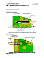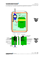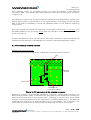
1
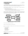
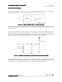
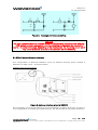
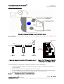
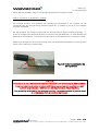
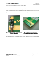
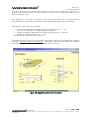
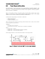
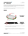
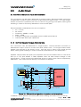
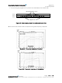
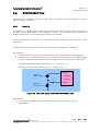
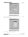
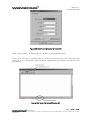
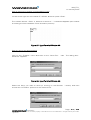
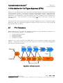
WISMO DESIGN GUIDELINES Reference : Level : Date : confidential © WM_FTA_GUIDELINES Version 1.0 13 January 2003 Page : 1 / 48 This document is the sole and exclusive property of WAVECOM. Not to be distributed or divulged without prior written agreement. WM_FTA_ 13 January 2003 Document Information Level Ver.1.0 Date History of the evolution 13/01/03 Written by Checked by Approved by Writer WISMO Design Guidelines Name David TAN Function Technical Support HW Group SW Group Christophe SEVEAU Deputy Director Engineering confidential © Date 13 Jan 2003 13 Jan 2003 Signature 13 Jan 2003 Page : 2 / 48 This document is the sole and exclusive property of WAVECOM. Not to be distributed or divulged without prior written agreement. WM_FTA_ 13 January 2003 Contents 1. Introduction 2. Hardware Design Consideration 2.1. RF Interface 2.1.1. Antenna Interface Characteristics 2.1.2. Antenna Matching 2.1.3. QUIK Module Antenna Interface 2.1.3.1. Antenna Connection of WISMO QUIK 2.1.3.2. Mechanical Connection of Coaxial Cable on QUIK 2.1.4. PAC Module Antenna Interface 2.1.5. General Design Guideline of Antenna Interface 2.2. Power Supply & Grounding 2.2.1. GPRS Class 2 VS Class 10 2.2.2. WISMO Grounding 2.3. SIM Interface 2.3.1. Mechanical Consideration of SIM Holder 2.3.2. SIM Card Voltage 2.4. Audio Circuit 2.4.1. Common Microphone Inputs Characteristics 2.4.2. Common Speaker Outputs Characteristics 2.5. BOOT/RESET Pins 2.5.1. Boot Pin 2.5.2. Reset Pin 2.6. Serial Interface 2.7. ESD Immunity 2.8. PCB Layout Suggestion 2.8.1. ESD Consideration 2.8.2. Layout Tactic against ESD 2.8.3. Mechanical Design Recommendations 2.8.4. Stretch Cabinet Wall 3. Software Design Consideration 3.1. SMS Design Consideration 3.2. IMEI Download 3.2.1. IMEI Number 3.2.2. Before Starting 3.2.3. Downloader Installation 3.2.4. Execute Downloader 3.3. Software Upgrade 3.3.1. Background Information 3.3.2. Upgrade Procedure (using HyperTerminal) 3.3.3. Recovery Procedure 4. Guideline for Full Type Approval (FTA) 4.1. FTA Procedure 4.2. FTA Phase Description 4.2.1. Product Definition Phase 4.2.2. Preliminary Phase 4.2.3. Evaluation Phase 4.2.4. Reaction Phase 4.2.5. Preparation Phase 4.2.6. Regulatory Testing Phase confidential © Page : 3 / 48 This document is the sole and exclusive property of WAVECOM. Not to be distributed or divulged without prior written agreement. WM_FTA_ 13 January 2003 4.2.7. Administrative Procedure confidential © Page : 4 / 48 This document is the sole and exclusive property of WAVECOM. Not to be distributed or divulged without prior written agreement. WM_FTA_ 13 January 2003 1.0 Introduction The aim of this document is to highlight important points from the design aspect that need to be taken into account and also provides some relevant information to client integrating Wavecom WISMO (QUIK or PAC series) in their application. When designing an application based on WISMO module, it is really important to consider the application field: Define what type of application. Consider the associated mechanical constrains. Consider the environment constrains (especially temperature) for the application and check if they are compatible with WISMO HW specification. Wavecom WISMO is designed as a plug-in module to fit in very small terminates and only some custom functions have to be added to make a complete wireless communicate solution, as shown below. For WISMO to function properly, attention should be pay on the design of these extra elements. Client’s Hardware Audio Interface RF Interface WISMO Serial Interface Power Supply SIM Interface Figure 1: External elements integrated with WISMO This document is divided into 4 sections. Section 1 is a brief introduction of this document. Section 2 concentrates on integration advices, PCB routing and components mapping for: Antenna Interface Power Supply SIM Interface Audio Circuit BOOT/RESET Pins Serial Interface ESD Immunity Section 3 covers the software aspect on: SMS confidential © Page : 5 / 48 This document is the sole and exclusive property of WAVECOM. Not to be distributed or divulged without prior written agreement. WM_FTA_ 13 January 2003 IMEI Download Software Upgrade The last section concerns about the application perform the Full Type Approval (FTA) test and Product Qualification test. Please Note: This document does not target to replace the Hardware specification that has to be read anyway carefully. 2.0 Hardware Design Consideration 2.1 RF Interface 2.1.1 Antenna Interface Characteristics When designing an antenna interface for the application, attention should be paid to: Choice of the antenna cable (type, length, performances, thermal resistance, & etc). Antenna choice Antenna connector (type + losses). These elements could affect GSM performances such as sensitivity and emitted power. Warning: Wavecom strongly recommends to work with an antenna manufacturer either to develop an antenna adapted to the application or to adapt an existing solution to the application. The antenna adaptation (mechanical and electrical adaptation) is one of the key issues in the design of a GSM terminal. The antenna interface circuit of QUIK and PAC series module is different. Refer to section 2.1.3 and 2.1.4 for more information of the antenna connection of WISMO modules. confidential © Page : 6 / 48 This document is the sole and exclusive property of WAVECOM. Not to be distributed or divulged without prior written agreement. WM_FTA_ 13 January 2003 2.1.2 Antenna Matching The goal of the matching circuit is to link the antenna (impedance ZA) to the receiver and transmitter access of the module (impedance ZL = 50 ohm real). Figure 2: Typical configuration of matching circuit The matching circuit is composed by four elements implemented (Figure 2) on the module connecting the “Antenna PAD” to the “Round PAD” (access to the receiver and the transmitter). The four elements of the matching circuit are not yet fixed (defined), and depend on each antenna and mechanical integration. The matching circuit must be verified in these frequency bandwidths (depends on the module used): E-GSM 900 (880 to 960 MHz), DCS 1800 (1710 to 1880 MHz) and PCS 1900 (1850 to 1990MHz). Module Impedance Figure 3: Equivalent schematic, the components must be defined Proper antenna matching is essential for WISMO module’s performance and ESD (Electrostatic Discharge) compatibility. It is a must to choose a matching circuit to keep the antenna “DC” connected to the ground. Two topologies are proposed: confidential © Page : 7 / 48 This document is the sole and exclusive property of WAVECOM. Not to be distributed or divulged without prior written agreement. WM_FTA_ 13 January 2003 Figure 4: Topology of antenna matching Warning: For each release of antenna, chassis (mechanical/grounding including metal coating), PCB, battery, antenna connection, and the matching components are needed to retune. In some of the case, depending of the modification, the matching circuit return may not be sufficient, an antenna modification will be necessary. 2.1.3 QUIK Module Antenna Interface The configuration of antenna interface circuit for 2C/2C2 and 2D series module is difference to each other. As shown below: WISMO QUIK 2C/2C2 series: Figure 5: Antenna interface circuit of 2C/2C2 The equivalent circuit of the matching circuit of 2C/2C2 is a same as shown in Figure 3. The configuration of matching components (Z1, Z2, Z3 and Z4) is the same as shown. confidential © Page : 8 / 48 This document is the sole and exclusive property of WAVECOM. Not to be distributed or divulged without prior written agreement. WM_FTA_ 13 January 2003 WISMO QUIK 2D series: Figure 6: Antenna interface circuit of 2D (Top View) The equivalent circuit of 2D matching circuit is slightly difference to 2C module, as shown below: To Antenna Pad Antenna Pad R "A" Z1 Z4 Round Pad Z2 Z2 Z3 Z1 Z3 ZL = 50Ω "A" Physical not connected Z4 ESD R Round Pad Ground Pad Ground Pad Ground Pad Figure 7a: Equivalent circuit of 2D matching circuit Ground Plane Figure 7b: PCB layout of the 2D matching circuit (Bottom View) The descriptions of the pads on antenna interface of QUIK series are: Antenna Pad: This pad is for antenna spring contact if matching component is on the module. Round Pad: A 50 Ohms interface for RF connection. Z1, Z2, Z3 and Z4 is a matching circuit component, the matching components of 2D is at the other side of the module (shown in the Figure 7b). Ground Pad: The grounding for antenna. 2.1.3.1 Antenna Connection of WISMO QUIK confidential © Page : 9 / 48 This document is the sole and exclusive property of WAVECOM. Not to be distributed or divulged without prior written agreement. WM_FTA_ 13 January 2003 There are two possible way to connect an antenna to the QUIK module: Direct connection of antenna to module For 2C/2C2 module, the antenna can directly be connected to the module on the “Antenna Pad” by using a spring contact (Figure 8). A matching circuit on the module must be equipped. For 2D module, the Antenna Pad and the Round Pad is disconnected physically. In order to configure the antenna directly to module, the gap between “A” Pad and Round Pad has to be soldered. See Figure 7a and 7b for more detail of the connection setup. Wavecom strongly recommend working with the antenna manufacturer for the proper value of the matching components. Figure 8: Antenna connection by spring contact Spring Contact Warning: An antenna is not a standard component it must be tune specifically for each product. Antenna matching must be checked with the same component supplies and part number as production. Different source may introduce miss-matching. If the matching is defined by the antenna supplier, it is recommended to provide a set of components from production warehouse. confidential © Page : 10 / 48 This document is the sole and exclusive property of WAVECOM. Not to be distributed or divulged without prior written agreement. WM_FTA_ 13 January 2003 Indirect connection of antenna through coaxial cable The antenna can be connected to the module through a coaxial wire. A matching circuit on the module is not necessary to equip. For 2D, the gap between the “A” Pad and Round Pad has to be physical disconnected. Figures below show some of the example of using coaxial cable for antenna connection. Figure 9a: Coaxial cable soldered on the top of the 2D module Figure 9b: New design of antenna connection for automotive application Next paragraph shows more detail of these coaxial cable connections on 2C/2C2 and 2D module. confidential © Page : 11 / 48 This document is the sole and exclusive property of WAVECOM. Not to be distributed or divulged without prior written agreement. WM_FTA_ 13 January 2003 2.1.3.2 Mechanical Connection of Coaxial Cable on QUIK For an antenna connected through a coaxial cable to QUIK module, the core of the cable must connected to the Round Pad, and the shielding of the cable must grounded to the Ground Pad, as shown below: WISMO QUIK 2C/2C2 Series: Solder shielding (ground contact mandatory) Solder shielding on this pad for machanical maintaining Cable shielding RF 50Ω Cable Connect coaxial cable (core) No components, only pads Figure 10a: Coaxial cable connected to 2C/2C2 module antenna interface WISMO QUIK 2D Series: Solder shielding (ground contact mandatory) RF 50Ω Cable Cable shielding Connect coaxial cable (core) Antenna Pad Figure 10b: Coaxial cable connected to 2D module antenna interface confidential © Page : 12 / 48 This document is the sole and exclusive property of WAVECOM. Not to be distributed or divulged without prior written agreement. WM_FTA_ 13 January 2003 For application has to put antenna matching components and antenna connection pad on the main PCB. See below Figures for the detail of the connection: Ante nna Connection Pad 50 Ω Round Pad Antenna Matching Circuit Connect coaxial cable to gorund Figure 11a: 50Ω Pad Example of Matching circuit on PCB WISMO RG178 Coaxial Cable MAIN PCB TOP VIEW SIDE VIEW BOTTOM VIEW Contact spring for antenna Matching components A Ground Via holes A B B A Connect cable shielding to ground This area must be free from ground plane or signal in any layers Ground Via holes Figure 11b: Close up of the matching circuit on PCB Ground plane Ground plane 50 ohm coax cable To WISMO Module confidential © Page : 13 / 48 This document is the sole and exclusive property of WAVECOM. Not to be distributed or divulged without prior written agreement. WM_FTA_ 13 January 2003 The matching circuit on the PCB must be as close as possible to the antenna connection pad. And coaxial cable and matching circuit must be grounded, as shown in Figure 11a. As indicated in Figure 11b, the ground plane must be as wide as possible. Please note that an open area (no ground plane, or any signal tracks in any layers) on the opposite side of the PCB is necessary to avoid the capacitive effect on the antenna matching components. The size of pads connected the matching components is around 3.5 x 3.5 mm, and the pads isolation from ground is 2mm (See the indication A and B in Figure 11b for more information). A particular attention has to be paid at the RF losses. Wavecom recommend that RF losses are to be less than 1 dB between the module output and application output. 2.1.4 PAC Module Antenna Interface WISMO PAC 3A/3AD series: The way to connect the antenna for WISMO PAC series is as shown below: Q35 Microstrip (50 Ohm) Gnd vias Matching circuit has to close to antenna Figure 12: RF connection to the antenna connector Wavecom strongly recommends additional matching components between the antenna and the RF output of WISMO PAC (pin Q35) for the application including an antenna like mobile phone and wireless PDA. Topology is a PI structure plus a serial element; components assume to be capacitors or inductors depending on the antenna matching (see section 2.1.2 Antenna Matching for more detail). But if the pad is 50 Ohms and is connected to 50 Ohms load, the matching circuitry is not needed. confidential © Page : 14 / 48 This document is the sole and exclusive property of WAVECOM. Not to be distributed or divulged without prior written agreement. WM_FTA_ 13 January 2003 The RF connection should be short enough to minimize losses and must have a characteristic impedance of 50 Ohms until F ≥ 2 GHz. A micro strip line, as above, or a strip line can be used. The geometry of the strip line (width of the track and isolation to ground) must be computed with PCB material dielectric properties and stacking height of the PCB. Example for 50 Ohms line calculation For a FR4 substrate with relative dielectric permittivity of r = 4.6 Bottom or inside layer is used as a ground plane Height of dielectric (between RF line and ground plane) = 300 µm Height of metal in the RF line = 17 µm Result: Width of the RF line is 530 µm. Freeware software for RF line impedance calculation can be downloaded from Agilent web site (http://www.agilent.com/view/rf). See below Figure for the AppCAD software (Please note, the calculation is for an example reference only). Figure 13: AppCAD software from Agilent confidential © Page : 15 / 48 This document is the sole and exclusive property of WAVECOM. Not to be distributed or divulged without prior written agreement. WM_FTA_ 13 January 2003 2.1.5 General Design Guideline of Antenna Interface The following list is the general guide line (applicable for QUIK and PAC if suit) which application designers have to consider while they are designing RF section. The antenna should be isolated as much as possible from the PCB circuitry (power supply, audio, SIM, digital). It is strongly recommended to shield the terminal. The length of coaxial cables should be reasonably short (application designer has to consider manufacturing processes and repair requirements). The components for Antenna Matching Circuit should have a good frequency response at or greater than 2GHz. Application designer should avoid placing components around the RF connection point on the main PCB and close to the RF lines. The RF cable should be placed as far as possible to audio section (audio amplifier, filter), and LCD circuit. If there is no more space to separate these circuits, it is better to separate the RF section from these circuits with a space of good ground. As a general recommendation, all components or chips operated at high frequencies (microprocessors, memories, DC/DC converter), or other active RF parts (FM receiver, GPS system) shall not be placed too close to the module. In such a case, correct supply and ground decoupling areas shall be designed and validated. The distance between the RF connection point of the main PCB and the Antenna Matching Circuit should be as short as possible. If the distance is long, micro strip line should be used (Freq >= 2GHz). Some signals like Vbatt and charger line may require some EMI/RFI decoupling: parallel 33pF capacitor close to the module, or a serial ferrite bead (or both to get better results). In case a ferrite bead is used, the recommendations given for the power supply connection must be carefully followed (high current capacity and low impedance). confidential © Page : 16 / 48 This document is the sole and exclusive property of WAVECOM. Not to be distributed or divulged without prior written agreement. WM_FTA_ 13 January 2003 2.2 Power Supply & Grounding The power supply is one of the key issues in the design of wireless terminal. The technical choice is highly dependant on the application field and the available overall dimensions. Several architectures are possible: linear regulators, switching regulator, DC-DC converter, or batteries. Due to the bursted emission, the power supply must be able to deliver high current peaks in a short time. During these peaks the ripple and the drop on the supply voltage must not exceed a certain limit (see below parameters). A weak power supply design could affect in particular: EMC performances Spurious emission Phase and frequency error When choosing power supply the following criteria must be met in order for the module to work at optimum performance. Condition: ¾ Average current is 355mA ¾ During the burst (577µs), 3.4Vminimum / 2A Max is mandatory Result: ¾ Vdrop max = 300mV ¾ Ripple max = 2mV at 200KHz (to avoid if possible) ¾ Ripple max = 50mV less than 200KHz Power supply waveform when observed at VBATT line during bursted. Figure 14: Waveform of the drop VBATT and max ripple authorized confidential © Page : 17 / 48 This document is the sole and exclusive property of WAVECOM. Not to be distributed or divulged without prior written agreement. WM_FTA_ 13 January 2003 Other than the criteria listed above, special attention should be paid to: Quality of the power supply: low ripple, PFM, or PSM systems should be avoided (PWM converter preferred). The width of the power track (at least 3mm). The number of via between two power tracks (at least 4 vias). The area of ground plate. When supplying the module with a battery, the internal impedance of the battery should be as low as possible. Include a low internal impedance of PCM (Protection Circuit Module) circuit for battery protection. The recommendation of the battery parameters are: ¾ Total impedance (cell + PCM + battery connector + PCB track) should be < 150m Ohms. Wavecom strongly recommended: Cell ≅ 70m Ohms PCM ≅ 50m Ohms (Max) Battery connector ≅ 20m Ohms PCB track ≅ 10m Ohms ¾ Over Charge Delay Time > 1.1s. 2.2.1 GPRS Class 2 VS Class 10 Due to the GPRS Class 10 has up to 2 uplink timeslot, and 3 downlink timeslot (3Rx/2Tx). The power consumption requires is higher than GPRS Class 2, which has one uplink timeslot, and 1 downlink timeslot (1Rx/1Tx) – Peak current is the same (2A Max), but average current is higher. Care should be pay on the power supply when design an application using GPRS Class 10 module. confidential © Page : 18 / 48 This document is the sole and exclusive property of WAVECOM. Not to be distributed or divulged without prior written agreement. WM_FTA_ 13 January 2003 2.2.2 WISMO Grounding The WISMO QUIK and PAC series is equipped with a shielding case, this case must be connected to the ground plane, acting as a protection to the internal components (i.e. RF circuit) from an external interference. The ground has to be connected on the mother board through a complete layer on the PCB. It is recommended to use a common ground plane for all signals (analog / digital / RF). Refer to section 2.8 for the ground plane of PCB. WISMO QUIK Ground Pin Figure 15a: Ground pins of WISMO WISMO Module Figure 15b: The ground pin has solder on both sides of PCB Soldering Points The grounding connection is done through the shielding only; the four ground pins have to be soldered to the ground plane. The ground pins has to be soldered on both sides of the PCB, as shown in Figure 15b. This is help to speed up the process of heat dissipation from the module. confidential © Page : 19 / 48 This document is the sole and exclusive property of WAVECOM. Not to be distributed or divulged without prior written agreement. WM_FTA_ 13 January 2003 WISMO PAC It is mandatory to route a complete ground plane on the PCB under the WISMO PAC. It has to be connected to all ground pins. The top side shielding of WISMO PAC series is achieved through the top metallic cover connected to the WISMO PAC internal ground plane. This one is connected through the WCGA (Wavecom Column Grid Array) connector to the application ground plane. The bottom side shielding of WISMO PAC series is achieved through the GND pins of the WCGA connector. It is strongly recommended to avoid routing any signals under the module. Any signal passing under the WISMO PAC shall be place under the ground plane, or only passing through a via holes. To ensure a good shielding of the module, a complete ground plane layer, as below, must be available, with no trade-off. Connections between others ground planes shall be done with vias. Without this ground plane, external TX spurious or Rx blockings could appear. Figure 15c: The ground pin has solder on both sides of PCB confidential © Page : 20 / 48 This document is the sole and exclusive property of WAVECOM. Not to be distributed or divulged without prior written agreement. WM_FTA_ 13 January 2003 2.3 SIM Interface For the SIM interface, length of the track between the module and the SIM connector should be as short as possible (preferable < 10cm). It is recommended to add Transient Voltage Suppression diodes on the signal connected to the SIM socket in order to prevent an Electrostatic Discharge (ESD) Æ Not applicable for WISMO 5. TVS diodes with low capacitance (less than 10pF) have to be connected on SIMCLK and SIMDATA to avoid any disturbance of the rising and falling edge. They shall be placed as close as possible to the SIM socket (see Figure 16). The following reference can be used: DALC208SC6 from ST Microelectronics. 100nF (1 ) (2 ) (3 ) (4 ) (5 ) (6 ) (7 ) (8 ) SIM V CC SIM RST SIM CLK V CC SIM D A T A SIM PRES 470pF 100K V CC RST CLK3 CC4 GN D V PP I/O CC8 SIM HOLDER ESDA-6V1L DALC208SC6 Figure 16: SIM with ESD When not used SIMPRES has to be tied to VCC. When used, a low to high transition means that the SIM card is inserted and a high to low transition means that the SIM card is removed. confidential © Page : 21 / 48 This document is the sole and exclusive property of WAVECOM. Not to be distributed or divulged without prior written agreement. WM_FTA_ 13 January 2003 2.3.1 Mechanical Consideration of SIM Holder Sequentially to prevent SIM failure/bad SIM contact to occur during the use of any application, it is strongly recommended to pay attention to SIM card holder design and ensure SIM contact properly. All applications should include a system to secure the contact by adding some pressure system on the back cover (cushion, nervures and etc), or create a “knob” on the battery to force the contact firmly between the SIM and the SIM holder pins (see examples below). An elastic “knob” is strongly recommended. Figure 17a : An example showing the “knob” created on the battery Figure 17b : This is how the “knob” pressing the SIM firmly contacts to the holder pin confidential © Page : 22 / 48 This document is the sole and exclusive property of WAVECOM. Not to be distributed or divulged without prior written agreement. WM_FTA_ 13 January 2003 2.3.2 SIM Card Voltage Below table shows the supported SIM voltage for WISMO QUIK and PAC: SIM Voltage WISMO 3 V SIM All QUIK series (2C, 2C2, 2D), and PAC series (3A, 3AD, 5). 5 V SIM Not supported by default. 1.8 V SIM Only PAC 5. In order to manage a 3V and 5V SIM in the application, Wavecom is recommended a solution by using an external level shifter (see Figure 18). Figure 18: Typical implementation of level shifter The activation of the LTC1555 (DVcc) is controlled by the WISMO module by connecting to module’s VCC; DDRV and DVcc should not be connected to SIMVCC. GPO0 and SIMVCC are used to control the voltage level for SIM card (3V or 5V). The following reference can be used: LTC1555 from Linear Technology Corporation. confidential © Page : 23 / 48 This document is the sole and exclusive property of WAVECOM. Not to be distributed or divulged without prior written agreement. WM_FTA_ 13 January 2003 2.3 Audio Circuit 2.4.1 Common Microphone Inputs Characteristics The connection can be either differential or single-ended. Recommended connection is differential in order to reject common mode noise and TDMA noise. If in case singleended connection is preferred, be sure to have a very good ground plane, filtering and shielding in order to avoid any disturbance on the audio path. Recommended characteristics for the microphone: 2.4.2 2V – 0.5mA 2K Ohms Sensitivity -38dB to -50dB SNR > 50dB Frequency response compatible with the GSM specifications Internal 33pF and 15pF capacitors Common Speaker Outputs Characteristics The connection can be differential or single-ended. Recommended connection is differential to reject common mode noise and TDMA noise. For single ended mode, please note that half of the power is lost. Also be sure to have a very good ground plane, filtering and shielding in order to avoid any disturbance on the audio path. Speaker outputs SPK2 are push-pull amplifiers and can be loaded down to 150 Ohms and up to 1nF (see details in table Speaker Gain VS Max Output Voltage in HW specification). These outputs are differential and the output power can be adjusted by 2dB steps. The output can be directly connected to a speaker. Internal Cap 15pF + 33pF Microphone 33pF 100nH 33pF 100nH 33pF 33pF MICxP 33pF MICxN 33pF WISMO Module ESD Diode 33pF 33pF Speaker 33pF ESD Diode 33pF SPKxP 33pF SPKxN 33pF Place to module pin as close as possible Place to Mic and Spk as close as possible Figure 19: Differential configuration of speaker and microphone In addition, some attention should be paid when dealing with audio circuit, such as: confidential © Page : 24 / 48 This document is the sole and exclusive property of WAVECOM. Not to be distributed or divulged without prior written agreement. WM_FTA_ 13 January 2003 When laying out the PCB, it is advisable to keep the audio circuit away from the VBATT line and antenna matching circuit (to avoid TDMA noise). If extra audio amplifier is needed to drive a speaker, it is recommended to prepare a dedicated speaker for WISMO module without passing through the amplifier; this will help to reduce the chance of TDMA noise build up in the application. If an application requires an audio amplifier to drive a loud speaker, and this speaker is share with WISMO and the application. Care should be taken in order to avoid TDMA noise built in the application. It is strongly recommended to use a speaker and microphone with correct frequency response. The detailed information is provided by ETSI 30.1-30.4. In order to reduce air leakage and make good frequency response, both speaker and microphone mechanical part must be added rubber cushions. See below. Figure 20: Another example microphone. of rubber cushion Connect all the audio grounding to the board’s main grounding. The positive and negative PCB track of speaker and microphone should keep in parallel all the time. When choosing microphones, it is recommended to use with internal capacitors (33pF and 15pF) to eliminate TDMA noise. confidential © Page : 25 / 48 This document is the sole and exclusive property of WAVECOM. Not to be distributed or divulged without prior written agreement. on WM_FTA_ 13 January 2003 Avoid routing any digital line or power line underneath of the audio lines. Microphone/Speaker tracks Layer 1 Layer 2 Layer 3 Digital tracks Figure 21: Avoid placing digital line underneath audio line Below shown the receiver and microphone with good frequency response: Figure 22: Frequency response of receiver Figure 23: Frequency response of microphone confidential © Page : 26 / 48 This document is the sole and exclusive property of WAVECOM. Not to be distributed or divulged without prior written agreement. WM_FTA_ 13 January 2003 2.5 BOOT/RESET Pins Please Note: In addition of the following, refer to module’s HW specification for the pin layout of Reset and Boot. 2.5.1 Boot Pin The BOOT pin is essential for Wavecom customer support team and used to download software in the Flash ROM of the WISMO module. The internal boot procedure is started when this pin is low during the reset of the module. Even this input pin is optional, it is recommended to implement this input pin in the application. There are number of ways to implement this, either by software or hardware. By hardware: A switch can be connected to the BOOT pin, this switch has to be accessible. The BOOT pin can be routed to serial connector and a special downloading cable can be manually activate the Boot and Reset pins, such as shown in Figure 24. Activate download mode: BOOT switch = 1, BOOT pin = 0. Activate normal mode: BOOT switch = 0, BOOT pin = 1. RESET RESET Switch WISMO 1K BOOT Switch Module BOOT Figure 24: Alternate way of implement Boot/Reset pins By Software: It is completely dependant of customer side to implement through its application. confidential © Page : 27 / 48 This document is the sole and exclusive property of WAVECOM. Not to be distributed or divulged without prior written agreement. WM_FTA_ 13 January 2003 2.5.2 Reset Pin It is recommended not to use this pin or only for emergency case. This signal is used to force a reset procedure by providing low level during at least 100us. It has to be considered as an emergency reset only, and driven by an open collector or an open drain, as shown in Figure 24. Activate reset mode: RESET switch = 1, RESET pin =0. This pin can not used as an On/Off switch. 2.6 Serial Interface A flexible 6 wires serial interface is available complying with V24 protocol signalling but not with V28 (electrical interface) due to a 2.8V interface. Four signal lines are mandatory, TXD, RXD, RTS and CTS. These signal lines are essential for serial communication, such as IMEI downloading, software upgrade, AT command testing and Tracer tools. Test points must be provided and easily accessible for validation (see Figure 25 for detail). Refer to module HW specification for the pin layout of the serial interface. VC TP5 TP3 TP6 TP4 WISMO Module TXD RXD uP CTS TP2 TP1 Figure 25: Serial link configuration confidential © Page : 28 / 48 This document is the sole and exclusive property of WAVECOM. Not to be distributed or divulged without prior written agreement. WM_FTA_ 13 January 2003 2.7 ESD Immunity Plastic enclosures, air space and insulation can prevent ESD arcs to equipment. Ensure >= 5mm path length between the electronics and - Any points that the user can touch, including seams, ventilation openings and mounting holes. At a given voltage, arcs can travel farther over the surface of a dielectric than they can through open air. - Any ungrounded metal that the user can touch-fasteners, switches, control and indicators. Cover seams and mounting holes with Mylar tape inside the enclosure, extending past the edge of the seam/hole, to increase the path length where clearance is limited. Cover unused or rarely used connectors with metal caps or insulating plastic dust covers. Use switched and controls with plastic shafts, or put plastic knobs or “tophats” on them, to increase the path length. Avoid knobs with metal setscrews. Recess LEDs and other indicators; cover them with tape or caps extending past the edge of the holes, or use light pipes to increase the path length. Extend the border on membrane keyboards >= 12mm outside the metal traces, or use a plastic bezel to increase the path length. Round the corners and edges on heat sinks and other metal parts that are close to seams, ventilating holes or mounting holes in the enclosure. Do not let metal fasteners protrude inside a plastic enclosure if they will be anywhere close to the electronics or ungrounded metal. Put taller feet on a product to raise it off the table/floor if the product fails indirect ESD tests to the table/floor or horizontal coupling plane. On tactile rubber keypads, keep the traces in tight and extend the rubber pieces to increase path length. Use adhesive/sealant around the circuitry layers of membrane keyboards. Use a high-voltage-proof silicone or poron gasket to provide an airtight, ESDproof, waterproof, dustproof seal between pieces of the enclosure. confidential © Page : 29 / 48 This document is the sole and exclusive property of WAVECOM. Not to be distributed or divulged without prior written agreement. WM_FTA_ 13 January 2003 2.8 PCB Layout Suggestions 2.8.1 ESD Consideration Circuit board layout is a critical design step in the suppression of ESD induced transients. The following guidelines are recommended: The ESD diodes should be placed as close as possible to the input terminals or connectors. All conductive loops, including power and ground loops should be minimized. The ESD transient return path to ground should be kept as short as possible. Ground planes should be used whenever possible. A main precaution to take is to put the protection device closer to the disturbance source (generally the connector). The path length between the ESD suppressor and the protected line should be minimized (see below Figure). GPC CONNECTOR Q2403 ESD DIODE GPC CONNECTOR Q2403 ESD DIODE CONNECTOR to external environment CONNECTOR to external environment PIN TO PROTECT PIN TO PROTECT Figure 26a: Shorter track to ESD Diode confidential © Figure 26b: Configured way to avoid Page : 30 / 48 This document is the sole and exclusive property of WAVECOM. Not to be distributed or divulged without prior written agreement. WM_FTA_ 13 January 2003 2.8.2 Layout Tactic against ESD For a better ESD (Electrical Static Discharge) protection, good grounding planes should be presented around the PCB. It is recommended to add the ground planes to Top and Bottom layers as figure below. The ground plane is marked by red colour. Best grounding will be achieved if the ground planes (marked by red colour) have many GND vias. It is recommended to increase the GND vias inside the red area. Figure 27: Top and Bottom Layers with ground plane 2.8.3 Mechanical Design Recommendations An air insulating layer should be existed for protecting from ESD damage. It is strongly recommended to increase the gap between PCB and casing. The gap should be at least 2mm. Figure 28: PCB is isolated by air insulating layer confidential © Page : 31 / 48 This document is the sole and exclusive property of WAVECOM. Not to be distributed or divulged without prior written agreement. WM_FTA_ 13 January 2003 2.8.4 Stretch Cabinet Wall To be a good isolation from the outside world, increasing the height of wall is very important against to ESD. There are two solutions to fabricate the front and rear cabinets. It is recommended to stretch the height of inner wall. They are illustrated by Figure 29 and 30. Figure 29: Stretch the height of inner wall Figure 30: Stretch the height of inner wall confidential © Page : 32 / 48 This document is the sole and exclusive property of WAVECOM. Not to be distributed or divulged without prior written agreement. WM_FTA_ 13 January 2003 3.0 Software Design Consideration 3.1 SMS Design Consideration For the application support SMS (Short Message Service) feature, it’s important for customer to ensure the application can handle GSM function when submitting or receiving Short Messages between application and a short message service centre. Table below shows all the 7-bit alphabets to be supported by SMS. The default alphabet is mandatory. Additional alphabets are optional. Irrespective of support of an individual alphabet, an application shall have the ability to store a short message coded in any alphabet on the SIM. Figure 31: 7-bit alphabets table For more information regarding the SMS alphabet coding, please refer to ETSI GSM 03.38 version. confidential © Page : 33 / 48 This document is the sole and exclusive property of WAVECOM. Not to be distributed or divulged without prior written agreement. WM_FTA_ 13 January 2003 3.2 IMEI Download This section shows how to use the Wavecom IMEI downloader for downloading the IMEI to the application. It’s important to follow the step-by-step show in the following paragraphs. 3.2.1 IMEI Number The IMEI number is composed of the following items: TAC: Type Approval Code FAC: Final Assembly Code VL: Version Level 3.2.2 Before Starting The IMEI downloading program is specific and adapted to only one user and one application. The user has to inform Wavecom to order his corresponding IMEI downloading program. In particular, the user must provide the following information concerning IMEI number assigned to him by official test lab: TAC: written on the FTA certificate of the application (6 digits). FAC: written on the FTA certificate of the application (2 digits). VL: Version Level of the application. A downloading speed (2400 Bps, 4800 Bps, 9600 Bps, 19200 Bps, 38400 Bps, 57600 Bps, 115200 Bps, auto-bauding). Com port for downloading. Wavecom will return the corresponding software including: A User_name: associated name to the downloading. A Password: used to protect the downloading procedure. N.B.: IMEI Downloader will not function if serial link is not properly implemented (RX/TX/RTS/CTS are mandatory). confidential © Page : 34 / 48 This document is the sole and exclusive property of WAVECOM. Not to be distributed or divulged without prior written agreement. WM_FTA_ 13 January 2003 3.2.3 Downloader Installation Step1: Copy the following files in the same directory: - setup.exe - ch_imei.001 - ch_imei.002 - user_name.bat1 - user_name.cfg1 1- See before starting paragraph to get the user_name Step2: Launch the user_name.bat executable program and follow the instruction. Once a dialog box appears with the words “WAVECOM: Writing IMEI installation successful!” you can click on the “OK” button to finish the installation. All the programming files have been stored in the folder of your choice (“wm_imei” by default). 3.2.4 Execute Downloader To Check the Version of Downloader To know the IMEI downloading program version, type the DOS command under the folder where is located the IMEI downloading program ch_imei.exe: Then the version number and its delivery date are written in the file “ret_code.txt”. Downloading the IMEI The program is protected by a password (refer to Before Starting section for password). To launch the download, type the DOS command under the folder where is located the IMEI downloading program ch_imei.exe: For example: ch_imei gsm 45645622123560 Once the program ran, a feedback code is returned in the “ret_code.txt” file. Refer to following table for the meaning of feedback code. Page : 35 / 48 confidential © This document is the sole and exclusive property of WAVECOM. Not to be distributed or divulged without prior written agreement. WM_FTA_ 13 January 2003 Figure 32: Table of feedback code After each successful downloading, all the information on this downloading is stored in the file user_name.txt (see the Before Starting paragraph to get the user_name). Important remarks: The IMEI number to download must be composed of the TAC, FAC and VL number corresponding to the user application. The module (modem) implemented in the user application must have a default IMEI number. It is recommend to reset the module (modem) implemented in the user application before starting the IMEI downloading program. confidential © Page : 36 / 48 This document is the sole and exclusive property of WAVECOM. Not to be distributed or divulged without prior written agreement. WM_FTA_ 13 January 2003 3.3 Software Upgrade This section covers the procedure and relevant information about the software (firmware) upgrading of WISMO GSM module. Warning: After finish downloading and power on WISMO, you have to wait for 10 seconds without carrying out any power off, download, rest, IMEI download allowing the auto initialization to be done, otherwise it is highly risky to corrupt parameters and damaged WISMO module. 3.3.1 Background Information The software package shall include the followings: Documentation: The AT software release note, informing you on the major modifications. The AT specification document corresponding to the software release (see Annex 1 for the links) Firmware (download in using Xmodem protocol or 1K Xmodem): pro-lib.dwl: The software release for WISMO module Configuration files: (some of those files may not exist depending on software version) wm12550.dwl: To set up the module to 900/1900 MHz bands wmmodem.dwl: To set up the external WMOD2 modem (force the audio 2 by default). This file shall not be downloaded for internal modem WMOi3. wm12792.dwl: Activate the Wavecom echo cancellation wm12793.dwl: Force the module in 900MHz band vxxx.dwl: Configure the software to the PCB version. Please check your PCB reference number by using the AT command: AT+WHWV. PCB version = yyy The following rules MUST be applied when downloading the vxxx.dwl file: Dowmload vxxx.dwl, if PCB hardware version yyy = xxx In other cases, download vzzz.dwl. Where zzz is the highest number just below yyy Example: If PCB version 4.27, yyy = 427 If the only available configuration files are: v400.dwl / v417.dwl / v500.dwl The only files which can be download is v417.dwl dwl.dwl: The latest downloader Wavecom strongly recommends updating the downloader. version can be checked with AT+WDWL? confidential © The downloader Page : 37 / 48 This document is the sole and exclusive property of WAVECOM. Not to be distributed or divulged without prior written agreement. WM_FTA_ 13 January 2003 Attention: If a problem occurs during the downloading of the firmware (accepted the downloader), please refer to the paragraph 3 for recovery process. If the sentence “BAD SOFTWARE” is sent through the serial link, at power up. It does not mean the software is “bad” or the download failed. The module cannot start and need to be unlocked. In such case send the module back to Wavecom for upgrade. If a problem happens during the downloading of the downloader, the module or modem cannot be downloaded anymore, it must be send to the nearest Wavecom support centre for recovery. 3.3.2 Upgrade Procedure (using HyperTerminal) Before Starting In the following example the connection is called “WM2C Download”. To start, the RS232 link is set up at 9600 Bps, with 8 data bits, no parity, one stop bit and a hardware flow control (RTS/CTS). The “COM1” is used as serial communication port. Step 1: Set up the download speed to 115200 Bps To speed up the download process, you can set up the communication speed at 115200 Bps maximum. Once you open the “Windows Hyper Terminal” program, on the screen type the command AT+IPR = 115200 and then press “Enter”. (That sets the speed on the module side). In the “File” menu, click on the “Properties” tab. The following dialog box appears on the screen. confidential © Page : 38 / 48 This document is the sole and exclusive property of WAVECOM. Not to be distributed or divulged without prior written agreement. WM_FTA_ 13 January 2003 Figure 33: Com port property window #1 Press the “Configure” button (just under the communication port). Properties” dialog box appears. The “COM1 Figure 34: Com port property window #2 Change the speed from 9600 Bps to 115200 Bps. confidential © Page : 39 / 48 This document is the sole and exclusive property of WAVECOM. Not to be distributed or divulged without prior written agreement. WM_FTA_ 13 January 2003 Figure 35: Com port property window #3 Press “Apply button”, and then the “OK” button on the next dialog box. To be sure the link is correctly set up; press the “Disconnect” icon and then the “Connect” icon. (“Windows Hyper Terminal” applies the new setting only after a new connection). Figure 36: HyperTerminal Window #1 confidential © Page : 40 / 48 This document is the sole and exclusive property of WAVECOM. Not to be distributed or divulged without prior written agreement. WM_FTA_ 13 January 2003 Step 2: Set up the module in downloading mode On the screen type the command AT+WDWL and then press “Enter”. The module answer +DWL: 0, and then a series of “ ” characters appears (the module is sending the first characters of the Xmodem protocol). Figure 37: HyperTerminal Window #2 Step 3: Launch the downloading Click on the “Transfer” menu and then on the “Send File …” tab. The dialog box “ Send File” appears. Figure 38: HyperTerminal Window #3 Select the file(1) you want to send (in clicking on the Browse…” button) and then choose the “Xmodem” protocol on the second line. confidential © Page : 41 / 48 This document is the sole and exclusive property of WAVECOM. Not to be distributed or divulged without prior written agreement. WM_FTA_ 13 January 2003 Figure 39: HyperTerminal Window #4 Click the “send” button. The following dialog box appears on the screen. Figure 40: HyperTerminal Window #5 You can see the downloading processing. The downloading lasts around 3 to 4 minutes, after that the dialog box closes automatically. Note: If you want to download two files in one operation (for example to configure the dual band external modem WMOD2), you can merge the files to download in using the DOS command “Copy” + the option “-b”: Ex: To create the new file “onefile.dwl”, type: Copy /b pro-lib.dwl + wmmodem.dwl onefile.dwl Step 4: Restart the module On the screen type: AT+CFUN=1 and then press “Enter”. The module is automatically set up to communicate at 9600 Bps with 8 data bits, no parity, one stop bit and a hardware flow control (RTS/CTS). Also to type AT command, you must set the communication port with those parameters. confidential © Page : 42 / 48 This document is the sole and exclusive property of WAVECOM. Not to be distributed or divulged without prior written agreement. WM_FTA_ 13 January 2003 In the “File” menu, click on the “Properties” tab. The dialog box “…properties” appears on the screen, press the “Configure” button (just under the communication port). The “COM1 Properties” dialog box appears. Change the speed from 115200 Bps to 9600 Bps. Press “Apply button”, and then the “OK” button on the next dialog box. To be sure the link is correctly set up; press the “Disconnect” icon and then the “Connect” icon. (“Windows Hyper Terminal” applies the new setting only after a new connection). Now, you can check the new software release in typing the command AT+CGMR + “Enter”. For example the module answers “401_M11B.55 ….” Is the software release is the V4.01. Figure 41: HyperTerminal Window #6 Note: The first restart can be little bit long from1-2 s up to 15-20s. 3.3.3 Recovery Procedure In case of failure or crash during the downloading process do the following: I. II. III. IV. V. VI. VII. Stay logged on your Windows Hyper Terminal session Hard reset the module or modem (connect the RESET pin to the ground) Then type continuously the capital letter “A” on your keyboard After few second the module or modem will echo the “A” Then type “AT” <CR> The module will respond either “ERROR” or “OK”, if “ERROR” it displays start again from the step v- until “OK” finally appears Finally follow the downloading procedure from the paragraph 2.3 Attention: confidential © Page : 43 / 48 This document is the sole and exclusive property of WAVECOM. Not to be distributed or divulged without prior written agreement. WM_FTA_ 13 January 2003 This procedure is not applicable if a failure occurs during the download of the downloader. If for whatever reasons, the recovery process does not work, the module or modem must be send to the nearest Wavecom support centre for recovery. confidential © Page : 44 / 48 This document is the sole and exclusive property of WAVECOM. Not to be distributed or divulged without prior written agreement. WM_FTA_ 13 January 2003 4.0 Guideline for Full Type Approval (FTA) Wavecom has obtained through international Notified Bodies a worldwide certification for the WISMO module. This allows a quicker and cheaper FTA (Full Type Approval) procedure for any product including a WISMO GSM/CDMA module. Based on this certification, any application using the WISMO will have to pass only a reduced set of validation tests. This procedure will last between shorter times than normal FTA procedure. Due to the FTA test is performed at the officially certified test house. Please be aware that there might be a significant lead-time to book a time-slot for FTA in any of the lab (typical lead-time: 6 weeks). 4.1 FTA Procedure Before starting the FTA tests, an evaluation phase is to be planned in Wavecom to check the customer’s design. The phases are: Product definition phase Preliminary phase Evaluation phase Preparation phase Wavecom will give a Go/No Go statement on the customer’s design after these phases. Figure 42 shows the FTA test sequence, and the following paragraphs discussed the phases in detail. Figure 42: FTA test sequence confidential © Page : 45 / 48 This document is the sole and exclusive property of WAVECOM. Not to be distributed or divulged without prior written agreement. WM_FTA_ 13 January 2003 4.2 FTA Phase Descriptions 4.2.1 Product Definition Phase Customer and Wavecom will get together to define applications features to cover both hardware and software part, in order to prevent any delay that could lead to gone astray market time. 4.2.2 Preliminary Phase After the project is defined, the customer is needed to submit a complete schematic diagram and PCB layout of the application for analysis. The document should include: Block diagram Product brief operation Gerber file Power PCB file (preferable in Power PCB V4). Once the preliminary checking is done, the customer is authorized to start to work on its prototype. This phase usually takes 1 week. 4.2.3 Evaluation Phase This phase will start once the customer is ready to provide a prototype, and this prototype must be built based on the recommendation or comment from Wavecom in preliminary phase, if it any. The aims of this phase are: To check if the product is ready to perform the FTA tests. To report any problem noticed during the expertise. To give advice on possible improvement. Customer is responsible to provide Wavecom with the following elements: At least 2 samples for an evaluation purpose. Reference handset, certified for telecom applications. A complete technical documentation: sample specification, user manual, MMI description and a list of oscillators used in the sample. Appropriate accessory such as: battery charger cable, communication cable, connectors and etc. CE Marking tests report and certificate. In addition, the sample submitted must have a fully tested and functional MMI (if the sample offers MMI capabilities). The sample must include a temporary access to the audio interface (MIC1/SPK1) of the module (if the sample offers audio capabilities). The application software should run even when external access activated (except the communication to the GSM module). This is to generate electronic activity on the confidential © Page : 46 / 48 This document is the sole and exclusive property of WAVECOM. Not to be distributed or divulged without prior written agreement. WM_FTA_ 13 January 2003 communication bus in order to validate the EMC performances in a nominal configuration. The application software will not be tested by Wavecom. The evaluation tests perform on the sample are: RF test Acoustic test SIM test ESD test SMS test TDMA noise test PCB impedance test Battery test Serial test Antenna matching test The phase period is very depends on customer’s design. 4.2.4 Reaction Phase For each of the evaluation, Wavecom recommends to the customer to stand back for a period of time to judge his product. The customer may realise some required modification on his design. The eventual changes will be checked and approved by Wavecom before the preparation phase. 4.2.5 Preparation Phase To past the FTA tests, at least 7 samples must be prepared at Wavecom: One One One One One One One product product product product product product spare for for for for for for RF conducted test RF radiated test acoustic tests, LVD tests safety tests SIM tests Once the samples are prepared, the samples will be tested using Wavecom’s test laboratory. Before sample go to the laboratory the customer must provide a folder including: The PIXIT files: this is a complete check list of the software use and embeds to run the product (e.g. MMI software). The final schematic: it has to be clean and easy to read, a BOM can be added. The product user guide or user manual (the one which will include in the sold box). Some PCBs details, such as fire class (for instance FR4 is the most common class). This folder will be submitted to the laboratory. confidential © Page : 47 / 48 This document is the sole and exclusive property of WAVECOM. Not to be distributed or divulged without prior written agreement. WM_FTA_ 13 January 2003 If the pre-test failed, the samples are returned to the customer with a complete report on the failure. Wavecom will help the customer to modify the product. Then the customer shall resubmit the samples for the preparation. 4.2.6 Regulatory Testing Phase Once the samples prepared and checked, Wavecom submits the samples to the authorized FTA test house and follows the whole testing at the test house. To speed up the process, one Wavecom engineer will stay during the tests at the test house. Only the final product, mass production unit is tested; the PCBs must be perfect NO jumping wire and NO soft tooling cabinet (pictures of the PCBs and the product are taken and keep by the laboratory for reference). The sample is tested using an external control unit to drive the module with AT commands. Nevertheless, on the request of the test house, some tests might be performed using the MMI. After test completed Wavecom can return the products to the customer, excepted one for reference (generally the one use during RF radiated test). 4.2.7 Administrative Procedure In parallel of the FTA technical process, the customer, with the support of Wavecom, must prepare the administrative approval procedure. This procedure is based on a folder including administrative and technical information. The folder includes form of PIXIT, IMEI Allocation and GSM application. Authorized test house will issue: GSM Test Report EMC report Safety Report Official Type Examination Certificate is issued in accordance with Annex IV of R&TTE Directive 1999/5/EC IMEI number Wavecom will then immediately after the tests completed deliver the IMEI numbers with the corresponding downloading software and a photocopy of the certificate to customer. confidential © Page : 48 / 48 This document is the sole and exclusive property of WAVECOM. Not to be distributed or divulged without prior written agreement.