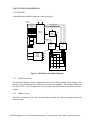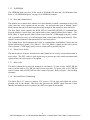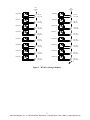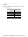
1
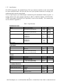
U S E R ’ S M A N U A L 16-CHANNEL FORM A SWITCH M-MODULE MODEL M218 (FORMERLY HP E2270A) Document Part No: 11029534 C&H Technologies, Inc. <> 445 Round Rock West Drive <> Round Rock, Texas 78681 <> www.chtech.com COPYRIGHT C&H Technologies, Inc. (C&H) provides this manual "as is" without warranty of any kind, either expressed or implied, including but not limited to the implied warranties of merchantability and fitness for a particular purpose. C&H may make improvements and/or changes in the product(s) and/or program(s) described in this manual at any time and without notice. This publication could contain technical inaccuracies or typographical errors. Changes are periodically made to the information herein; these changes will be incorporated in new editions of this publication. Copyright © 2006 by C&H Technologies, Inc. Portions of this manual have been copied from relevant Hewlett-Packard (Agilent) User Manual’s with their expressed written permission. The information and/or drawings set forth in this document and all rights in and to inventions disclosed herein which might be granted thereon disclosing or employing the materials, methods, techniques, or apparatus described herein, are the exclusive property of C&H Technologies, Inc. A Reader's Comment Form is provided at the back of this publication. If this form has been removed address comments to: C&H Technologies, Inc. Technical Publications 445 Round Rock West Drive Austin, Texas 78681-5012 Or visit our web site for support information at: http://www.chtech.com. C&H may use or distribute any of the information you supply in any way that it believes appropriate without incurring any obligations. ii C&H Technologies, Inc. <> 445 Round Rock West Drive <> Round Rock, Texas 78681 <> www.chtech.com AMENDMENT NOTICE C&H Technologies, Inc. makes every attempt to provide up-to-date manuals with the associated equipment. Occasionally, changes are made to the equipment wherein it is necessary to provide amendments to the manual. If any amendments are provided for this manual they are printed on colored paper and will be provided with the module and manual. Manual updates may also be found on out web site at www.chtech.com. NOTE The contents of any amendment may affect operation, maintenance, or calibration of the equipment. iii C&H Technologies, Inc. <> 445 Round Rock West Drive <> Round Rock, Texas 78681 <> www.chtech.com INTRODUCTION This manual describes the operation and use of the C&H Model M218 16-Channel Form A Switch M-Module (Part Number 11029530). This module was formerly manufactured by HP (Agilent) as Model E2270A. C&H obtained the manufacturing rights from Agilent and now manufacturers it as C&H Model M218. This mezzanine module is designed to interface within any M/MA-Module carrier adhering to the ANSI/VITA 12-1996 M-Module specification. These carriers are available in many formats such as Ethernet, VME, VXI, PXI, cPCI, and the PC. Contained within this manual are the physical and electrical specifications, installation and startup procedures, functional description, and configuration and programming guidelines to adequately use the product. This manual is based on a low level register access, and is written in such a manner to provide understanding to the user based on this type of access. If a driver is provided, please refer to the driver documentation for instruction using the higher level interface provided by the driver. iv C&H Technologies, Inc. <> 445 Round Rock West Drive <> Round Rock, Texas 78681 <> www.chtech.com TABLE OF CONTENTS 1.0 GENERAL DESCRIPTION................................................................................................ 1 1.1 PURPOSE OF EQUIPMENT ................................................................................... 1 1.2 SPECIFICATIONS OF EQUIPMENT...................................................................... 1 1.2.1 Key Features ............................................................................................ 1 1.2.2 Specifications ........................................................................................... 2 1.2.3 Mechanical............................................................................................... 3 1.2.4 Bus Compliance ....................................................................................... 3 1.2.5 Applicable Documents.............................................................................. 3 2.0 INSTALLATION................................................................................................................ 5 2.1 UNPACKING AND INSPECTION .......................................................................... 5 2.2 HANDLING PRECAUTIONS.................................................................................. 5 2.3 INSTALLATION OF M/MA MODULES................................................................. 5 2.4 PREPARATION FOR RESHIPMENT...................................................................... 6 3.0 FUNCTIONAL DESCRIPTION ......................................................................................... 7 3.1 OVERVIEW ............................................................................................................. 7 3.1.1 M-Module Interface ................................................................................. 7 3.1.2 Module Control........................................................................................ 7 3.1.3 ID EEPROM............................................................................................ 8 3.1.4 Row and Column Drivers ......................................................................... 8 3.1.5 Driver Power Switch................................................................................ 8 3.2 IDENTIFICATION AND CONFIGURATION REGISTERS ................................. 10 3.2.1 I/O Registers.......................................................................................... 10 3.2.2 Module Identification ............................................................................. 13 4.0 OPERATION.................................................................................................................... 14 4.1 FIFO STRUCTURE................................................................................................ 14 4.2 RELAY SET/RESET .............................................................................................. 14 4.3 MATRIX DRIVE TO CHANNEL MAPPINGS ...................................................... 15 4.4 INTERRUPTS ........................................................................................................ 15 APPENDIX A: CONNECTORS ............................................................................................ A-1 v C&H Technologies, Inc. <> 445 Round Rock West Drive <> Round Rock, Texas 78681 <> www.chtech.com LIST OF FIGURES Figure 1. Figure 2. Figure 3. Figure 4. M-MODULE Installation ............................................................................................ 5 M218 Functional Block Diagram................................................................................. 7 M218 Switching Schematic ......................................................................................... 9 M218 I/O Registers................................................................................................... 11 Figure A-1. Front Panel I/O Signals......................................................................................... A-1 LIST OF TABLES Table I. Specifications ................................................................................................................ 2 Table II. I/O Address Map/Command Summary....................................................................... 10 Table III. M/MA Module PROM IDENT Words...................................................................... 13 Table IV. Matrix Drive............................................................................................................. 15 vi C&H Technologies, Inc. <> 445 Round Rock West Drive <> Round Rock, Texas 78681 <> www.chtech.com 1.0 GENERAL DESCRIPTION The M218 provides 16 one-wire switches on a single wide M-Module adhering to the ANSI/VITA 12-1996 specification for M-Modules. The M218 may be installed on any carrier board supporting the M-Module specification. Carriers are available that allow the M218 to be used in Ethernet, VXI, VME, PCI, cPCI and other system architectures. 1.1 PURPOSE OF EQUIPMENT The M218 is a general purpose relay switch that can be used to connect test points on a device under test to instrumentation or to switch factory automation and fixturing. CAUTION: This module uses latching relays that retain their last programmed state whenever power is removed (closed relays will remain closed until opened via your test program). CAUTION: This module DOES NOT have provisions for on-board current limiting components (if input current can exceed 2A DC or 2A AC, you must install external current limiting circuitry) 1.2 SPECIFICATIONS OF EQUIPMENT 1.2.1 Key Features 16 Latching Relays Connector Type: 44-pin D-Sub Interrupts when requested relay movements have completed Latching relays retain last programmed state FIFO register structure allows fast system operation Single-width M-Module provide high-density and maximum flexibility of configuration 1 C&H Technologies, Inc. <> 445 Round Rock West Drive <> Round Rock, Texas 78681 <> www.chtech.com 1.2.2 Specifications The M218 incorporates the standard 40-pin, 20x2 row connector interfaces to the carrier board for power and data/control, but does not have the 24-pin optional connector for carrying userconnections back onto the carrier board. The user input/output is provided through a standard 44-pin D-subminiature female receptacle. A mating connector kit can be ordered separately as AM111 (C&H Part Number 11029700-0001). CONEC part number 302A10889X (or equivalent) is used on the assembly. The connector pinouts are shown in Appendix A. Table I. Specifications MAXIMUM RATINGS Parameter Condition Voltage Clean room Environment (any terminal to any other terminal) Rating Units Current (non-inductive) Per Switch, DC Per Switch, AC Per Module, DC Per Module, AC 200 125 175 60 48 68 2 2 8 8 Power Per Switch, DC Per Switch, AC Per Module, DC Per Module, AC 50 50 200 200 W VA W VA < 3 typ µV Non-Clean room Environment (any terminal to any other terminal) Thermal Offset VDC VACrms VAC peak VDC VACrms VAC peak A A peak A A peak RESISTANCE Parameter Condition Closed Channel Initial End of Life Between any two points ≤40°C, ≤65% relative humidity ≤25°C, ≤40% relative humidity Insulation Rating < 0.2 typ <2 Units 10 typ 8 10 typ Rating Units 8 RELAYS Parameter Condition Relay Life Time to open/close Insulation at rated load register programming Between any two points ≤40°C, ≤65% relative humidity ≤25°C, ≤40% relative humidity 5 10 8 8 10 typ 8 10 typ operations ms AC CHARACTERISTICS Parameter Condition Typical Bandwidth Crosstalk (channel-to-channel) -3dB <100 KHz <1 MHz <10 MHz Channel-to-Channel Channel-to-Common Closed Channel Capacitance Rating > 10 -64 typ -44 typ -24 typ < 15 typ < 25 typ Units MHz dB dB dB pF pF 2 C&H Technologies, Inc. <> 445 Round Rock West Drive <> Round Rock, Texas 78681 <> www.chtech.com 1.2.3 Mechanical The mechanical dimensions of the module are in conformance with ANSI/VITA 12-1996 for single-wide M-Module modules. The nominal dimensions are 5.687” (144.5 mm) long 2.082” (52.9 mm) wide. 1.2.4 Bus Compliance The module complies with the ANSI/VITA 12-1996 Specification for single-wide M-Modules and the MA-Module trigger signal extension. The module also supports the optional IDENT and VXI-IDENT functions. Module Type: Addressing: Data: Interrupts: DMA: Triggers: Identification: Manufacturer ID: Model Number: VXI Model Number: M-Module A08 D16 supported not supported not supported IDENT 0FFF16 (See note below) 068616 025B16 Note: C&H obtained the manufacturing rights from Hewlett Packard (Agilent) for this module. The ID’s have been retained as Hewlett Packard to provide compatibility with existing SW drivers. 1.2.5 Applicable Documents ANSI/VITA 12-1996 Standard for The Mezzanine Concept M-Module Specification, Approved May 20, 1997, American National Standards Institute and VMEbus International Trade Association, 7825 E. Gelding Dr. Suite 104, Scottsdale, AZ 85260-3415, http://www.vita.com 3 C&H Technologies, Inc. <> 445 Round Rock West Drive <> Round Rock, Texas 78681 <> www.chtech.com 4 C&H Technologies, Inc. <> 445 Round Rock West Drive <> Round Rock, Texas 78681 <> www.chtech.com 2.0 INSTALLATION 2.1 UNPACKING AND INSPECTION Verify that there has been no damage to the shipping container. If damage exists then the container should be retained, as it will provide evidence of carrier caused problems. Such problems should be reported to the shipping courier immediately, as well as to C&H. If there is no damage to the shipping container, carefully remove the module from its box and anti static bag and inspect for any signs of physical damage. If damage exists, report immediately to C&H. 2.2 HANDLING PRECAUTIONS The module contains components that are sensitive to electrostatic discharge. When handling the module for any reason, do so at a static-controlled workstation, whenever possible. At a minimum, avoid work areas that are potential static sources, such as carpeted areas. Avoid unnecessary contact with the components on the module. 2.3 INSTALLATION OF M/MA MODULES All M-Modules must be installed into the carrier before the carrier is installed into the host system. To install a module, firmly press the connector on the M/MA-Module together with the connector on the carrier as shown in Figure 1. Secure the module through the holes in the bottom shield using the original screws. CAUTION: M/MA-Module connectors are NOT keyed. Use extra caution to avoid misalignment. Applying power to a misaligned module can damage the M/MA-Module and carrier. M/MA-Module A B Row not used Carrier Figure 1. M-MODULE Installation 5 C&H Technologies, Inc. <> 445 Round Rock West Drive <> Round Rock, Texas 78681 <> www.chtech.com 2.4 PREPARATION FOR RESHIPMENT If the module is to be shipped separately it should be enclosed in a suitable water and vapor proof anti-static bag. Heat seal or tape the bag to insure a moisture-proof closure. When sealing the bag, keep trapped air volume to a minimum. The shipping container should be a rigid box of sufficient size and strength to protect the equipment from damage. If the module was received separately from a C&H system, then the original module shipping container and packing material may be re-used if it is still in good condition. 6 C&H Technologies, Inc. <> 445 Round Rock West Drive <> Round Rock, Texas 78681 <> www.chtech.com 3.0 FUNCTIONAL DESCRIPTION 3.1 OVERVIEW A simplified functional block diagram is shown in Figure 2. VCC Carrier Interface DGND A(7:1) ROW _SET(4:1) D(15:0) ROW _RESET(4:1) /CS /IACK VCC /WRITE /DS0 /DS1 Module Control SYSCLK /DTACK Driver Power Switch DR_EN /IRQ +5VDR /RST ROM COL(4:1) ID EEPROM +12V /DACK /DREQ N.C. Column Drivers N.C. N.C. COL_DR(4:1) +5V GND /RESET Row Drivers ROW_DR(4:1) VCC Reset & Power Supply Conditioning DGND ZGND /RST Relay Coils Figure 2. M218 Functional Block Diagram 3.1.1 M-Module Interface The M-Module Interface allows communication between the M218 and the carrier module. The interface is an asynchronous 16-bit data bus with interrupt capabilities. The interface adheres to the ANSI/VITA 12-1996 Standard for The Mezzanine Concept M-Module Specification for MA modules. 3.1.2 Module Control This block contains all of the logic for the module including all registers, interrupt control and carrier interface. 7 C&H Technologies, Inc. <> 445 Round Rock West Drive <> Round Rock, Texas 78681 <> www.chtech.com 3.1.3 ID EEPROM The EEPROM holds sixty-four 16-bit words of M-Module ID data and VXI M-Module data. Refer to “ID EEPROM Register” on page 10 for EEPROM contents. 3.1.4 Row and Column Drivers The module uses a matrix drive scheme (rows and columns) in which a maximum of four of the relays (one row) can be operated at any one time. An on-board timer (part of Module Control block) ensures the relay coils have been driven long enough for the contacts to move and settle. The Row Driver block translates the ROW_SET(4:1) and ROW_RESET(4:1) command lines from the Module Control block into bipolar and tri-state capable buffered drive signals. The ROW_DR(4:1) signals provide either current source from the +5VDR supply (relay set), current sink to ground (relay reset), or tri-stated output (both current-source and current-sink off). Each output is tri-stated whenever that particular row is not being driven. The Column Driver block translates the COL(4:1) command lines from Module Control into the bipolar buffered drive signals, COL_DR(4:1). The COL_DR(4:1) signals provide either current source from the +5VDR supply (relay reset) or current sink to ground (relay set). 3.1.5 Driver Power Switch This block removes all power from the Row and Column Driver circuitry except when needed to move relays. This FET switch is open at power-up to prevent any relay contact movement until register writes cause drive-power to be applied. 3.1.7 Relay Coils This block contains the 16 relay coils arranged as a 4x4 matrix. To close a relay, a ROW_DR line sources current while a COL_DR line sinks current to ground. To open a relay, a COL_DR line sources current while a ROW_DR line sinks current to ground. Refer to Figure 3 for switching schematic. 3.1.8 Reset and Power Conditioning This block filters +5V power to produce VCC power (+5V) for logic and isolates the various grounds used by the module. This block also processes the /RESET signal from the Carrier Interface and monitors power to produce the /RST reset signal for the module. 8 C&H Technologies, Inc. <> 445 Round Rock West Drive <> Round Rock, Texas 78681 <> www.chtech.com User Connector Pins User Connector Pins Channel 0 Channel 8 1 16 CH0_NO CH0_COM 2 17 CH1_NO CH1_COM 3 18 CH2_NO CH2_COM 4 19 CH3_NO CH3_COM 5 20 CH4_NO CH4_COM 6 21 CH5_NO CH5_COM 7 22 CH6_NO CH6_COM 8 23 CH7_NO CH7_COM Channel 1 9 24 CH8_NO CH8_COM 10 25 CH9_NO CH9_COM 11 26 CH10_NO CH10_COM 12 27 CH11_NO CH11_COM 13 28 CH12_NO CH12_COM 14 29 CH13_NO CH13_COM 15 30 CH14_NO CH14_COM 43 44 CH15_NO CH15_COM Channel 9 Channel 2 Channel 10 Channel 11 Channel 3 Channel 4 Channel 12 Channel 5 Channel 13 Channel 14 Channel 6 Channel 7 Channel 15 31 - 42 Figure 3. M218 Switching Schematic 9 C&H Technologies, Inc. <> 445 Round Rock West Drive <> Round Rock, Texas 78681 <> www.chtech.com 3.2 IDENTIFICATION AND CONFIGURATION REGISTERS 3.2.1 I/O Registers There are a variety of registers used to configure and control the module. These registers are located in the IOSpace. The address map of the registers is shown in Table II. Details of the registers are provided in Figure 4. Table II. I/O Address Map/Command Summary Register Name 00h 02h 04h-0Eh 10h 12h 14h 16h 18h 1Ah 1Ch 1Eh 20h - 7Eh 80h - FEh Status Register Control Register Reserved Row 0 Set Register Row 0 Reset Register Row 1 Set Register Row 1 Reset Register Row 2 Set Register Row 2 Reset Register Row 3 Set Register Row 3 Reset Register Unused ID EEPROM Register Type Read Only Read/Write NA Read/Write Read/Write Read/Write Read/Write Read/Write Read/Write Read/Write Read/Write NA Read/Write FIFO-able Register (Y/N) N N N Y Y Y Y Y Y Y Y N N 10 C&H Technologies, Inc. <> 445 Round Rock West Drive <> Round Rock, Texas 78681 <> www.chtech.com Reg. 00 Bit Write Read Status 15 14 13 12 11 10 9 7 6 5 4 3 INIT MPS 2 1 0 Read-only Reserved INIT MPS FIFOE FIFOF INT FIFOE FIFOF INT Init Status (1 = initialized since last power up, 0 = not initialized since last power up) Multiplexer Size (Not used on M218) FIFO Empty Status (1 = FIFO currently empty, up to 8 writes available and not busy) FIFO Full Status (1 = FIFO currently full, additional writes are lost) Interrupt Status (if enabled; 1 = interrupt line asserted, 0 = interrupt line not asserted) Reg. 02 Bit Write Read 8 Control 15 14 13 12 11 10 9 8 7 Reserved 6 5 4 TM 3 2 1 0 DPE STE INTE RST Reserved TM Timer Mode (proper operation is guaranteed only for the time = 8ms) 0 0 8ms 0 1 2ms 1 0 4ms 1 1 64ms DPE Driver Power Enable (1 = enables power to relay drivers, 0 = removes power) STE Self-Test Enable (1 = disable power to all row & column drivers and allows testing the operation of the FIFO without causing relay movement, 0 = allows row & column drivers to be powered (if driver power is enabled). Be sure the FIFO is empty before returning this bit to 0. INTE Interrupt Enable (1 = enables interrupts, 0 = disables interrupts) RST Reset (1 = initiates a soft reset, 0 = releases module from reset condition) Figure 4. M218 I/O Registers 11 C&H Technologies, Inc. <> 445 Round Rock West Drive <> Round Rock, Texas 78681 <> www.chtech.com Reg. 10 Bit Write Read Row 0 Set Register 15 14 13 12 11 10 9 Unused Unused 15 14 13 12 11 10 9 Unused Unused 15 14 13 12 11 10 9 Unused Unused 15 14 13 12 11 10 9 Unused Unused 15 14 13 12 11 10 9 Unused Unused 15 14 13 12 11 10 9 Unused Unused 15 14 13 12 11 10 9 Unused Unused 15 14 13 12 11 10 9 Unused Unused Reg. 12 Bit Write Read 8 7 6 5 4 3 2 1 0 R0C3 R0C2 R0C1 R0C0 R0C3 R0C2 R0C1 R0C0 8 7 6 5 4 3 2 1 0 R1C3 R1C2 R1C1 R1C0 R1C3 R1C2 R1C1 R1C0 8 7 6 5 4 3 2 1 0 R1C3 R1C2 R1C1 R1C0 R1C3 R1C2 R1C1 R1C0 8 7 6 5 4 3 2 1 0 R2C3 R2C2 R2C1 R2C0 R2C3 R2C2 R2C1 R2C0 8 7 6 5 4 3 2 1 0 R2C3 R2C2 R2C1 R2C0 R2C3 R2C2 R2C1 R2C0 5 4 3 2 1 0 R3C3 R3C2 R3C1 R3C0 R3C3 R3C2 R3C1 R3C0 5 4 3 2 1 0 R3C3 R3C2 R3C1 R3C0 R3C3 R3C2 R3C1 R3C0 Row 3 Set Register Reg. 1E Bit Write Read 3 2 1 0 R0C3 R0C2 R0C1 R0C0 R0C3 R0C2 R0C1 R0C0 Row 2 Reset Register Reg. 1C Bit Write Read 4 Row 2 Set Register Reg. 1A Bit Write Read 5 Row 1 Reset Register Reg. 18 Bit Write Read 6 Row 1 Set Register Reg. 16 Bit Write Read 7 Row 0 Reset Register Reg. 14 Bit Write Read 8 8 7 6 Row 1 Reset Register 8 7 6 RxCy Row x, Column y (1 = close relay, 0 = open relay) Note: The Switch M-Modules use a row and column relay drive scheme. To close a particular relay, write a logic “1” to the corresponding column in a Row n Set register. To open a relay, write a logic “0” in the corresponding column in a Row n Reset register. For example, to close the Channel 04 relay on the M218 (Row 1, Column 0 in relay drive scheme) place a logic “1” in bit 00 of the Row 1 Set register. To open this relay, place a logic “0” in bit 00 of the Row 1 Reset register. Table V shows the correlation of the matrix drive rows and columns to Switch M-Module channels. Figure 4. M218 I/O Registers (continued) 12 C&H Technologies, Inc. <> 445 Round Rock West Drive <> Round Rock, Texas 78681 <> www.chtech.com 3.2.2 Module Identification The M218 supports the identification function called IDENT. This IDENT function provides information about the module and is stored in a sixteen-word deep (32 byte) serial PROM. Access is accomplished with read/write operations on the last address in IOSpace (hex FE) and the data is read one bit at a time. The PROM is compatible with a standard IC 9603 type PROM. For specific timing information refer to the 9603 or compatible PROM data sheet. Data should not be written to the PROM. The module also supports the VXI-IDENT function. This function is not part of the approved ANSI/VITA 12-1996 standard. This extension to the M-module IDENT function increases the size of the PROM to 64 words and includes VXI compatible ID and Device Type Registers. Details are shown in Table III. Table III. M/MA Module PROM IDENT Words Word 0 1 2 3 4-7 8-15 16 17 18 19-31 32-63 Description Sync Code Module Number Revision Number 1 Module Characteristics 2 Reserved M-Module Specific VXI Sync Code VXI ID VXI Device Type 3 Reserved M-Module Specific Value (hex) 5346 0686 0001 0868 0000 0000 ACBA 0FFF 3 F25B (M218) 0000 0000 Notes: 1) The Revision Number is the functional revision level of the module. It does not necessarily correspond to the hardware assembly level. 2) The Module Characteristics bit definitions are: Bit(s) Description 15 0 = no burst access 14/13 unused 12 0 = does not need 12V 11 1 = needs +5V 10 0 = no trigger outputs 9 0 = no trigger inputs 8/7 00 = no DMA requestor 6/5 11 = interrupt type 4/3 01 = 16-bit data 2/1 00 = 8-bit address 0 0 = no memory access 3) The VXI ID of 0xFFF is the identification value for Hewlett-Packard. C&H has left the ID equal to this value to allow operation with existing E2270A software drivers. The revision number (see note 1) can be used to identify the module as manufactured by C&H. 4) The VXI Device Type word contains the following information: Description Bit(s) 15-12 F16 = 256 bytes of required memory 11-0 26016 = C&H specified VXI model code for M218 13 C&H Technologies, Inc. <> 445 Round Rock West Drive <> Round Rock, Texas 78681 <> www.chtech.com 4.0 OPERATION The M218 is a register-based instrument that is controlled through a series of I/O registers described in Section 3.2.1. The exact method of accessing and addressing the I/O registers is dependent on the M-Module carrier used to interface the module to your data acquisition or test system. Refer to the carrier’s documentation for information on the address mapping of an MModule’s I/O registers and to your system software documentation for details on data access. Typically a high level driver is available to aid in control of the module. Refer to the software driver documentation for instructions on using the driver. 4.1 FIFO STRUCTURE The FIFO (First-In-First-Out) structure allows multiple writes to the module to be stacked-up. This helps reduce interrupt overhead by allowing an interrupt only after the completion of the last relay operation in a sequence of up to eight operations. Eight was chosen because it allows at least one open and one close to each of the four relay rows, allowing a complete change of all relay states. If the M-Module is enabled to interrupt, it asserts the INT line on the M-Module interface to the Carrier when the last commanded relay operation in the FIFO has completed. For example, if relays in only one row were instructed to move, the module asserts an interrupt after that one row has been driven. If four rows were instructed to move (four writes to the FIFO--see note below), then the module asserts an interrupt only after the completion of the fourth operation. Note: The module asserts an interrupt after the relay drive time is complete (relay drive timer) and no other operations have been stored in FIFO. The above example assumes the four writes are stored in FIFO one after the other with very little time between the writes. If, in the above example, the amount of time between writes is greater than the relay drive time (8 ms), the module would actually interrupt four times--one interrupt after driving each relay. 4.2 RELAY SET/RESET When the FIFO is empty (no relay operations pending) bits 03, 02, 01, and 00 in the above registers indicate the state of the corresponding relay. Logic “1” means the relay in Row n Column n is closed or soon will be (depending on the FIFO Empty Status bit’s state). Logic “0” means the corresponding relay is open. Following are some general notes on relay operation: 1. Writing to a Row n Set register closes the relays only in the bit positions set to logic “1.” Writing logic “0” to a Row n Set register has no effect on relay position. Writing to a Row n Reset register opens relays only for the bit positions set to logic “0.” Writing logic “1” to a Row n Reset register has no effect on relay position. 2. Reading either the Row n Set or Row n Reset register addresses returns identical data because they are actually mapped to the same register. When you write to one of these registers (and FIFO is not full), the data is stored in the register and stored in FIFO. 14 C&H Technologies, Inc. <> 445 Round Rock West Drive <> Round Rock, Texas 78681 <> www.chtech.com 3. The Row n Set/Reset readback registers return the programmed relay state only if you use the module correctly. Since the driver power can be disabled (the power-on state), the Row n Set and Row n Reset registers can be written to and read from without moving any relay contacts. 4. When the module loses power, any closed relays remain closed (latching relays). When power is restored, the relays remain closed but the Row n Set and Row n Reset registers have lost their relay state information. This relay information is lost whenever power is cycled or the carrier asserts /RESET. You must initialize the module after a power-up or /RESET to achieve correlation between the Row n Set/Reset readback registers and the actual relay positions. To initialize the module: a. Enable driver power. b. Write all four column bits to zero in each Row n Reset register. You can check for initialization by reading the Init Status bit. If the module has not been initialized since the last power-up or /RESET, the Init Status bit will be logic “0”. The Init Status bit is set to logic “1” whenever the module has been successfully initialized. 1. To guarantee break-before-make relay operation, write to the Row n Reset registers before writing to the Row n Set registers. 2. It is important to use the FIFO status bits when writing to the Row n Set/Reset registers, especially when writing in bursts (such as when resetting the module’s relays). Writing to a Row n Set/Reset register when the FIFO is full results in the loss of data since the FIFO has no room to hold it. You should always check the FIFO FULL status to ensure that FIFO is not full before writing to a Row n Set/Reset register. 4.3 MATRIX DRIVE TO CHANNEL MAPPINGS Table IV correlates the matrix drive rows and columns to channel numbers on the M218. Table IV. Matrix Drive Matrix Drive Column 0 Column 1 Column 2 Column 3 Row 0 Channel 0 Channel 1 Channel 2 Channel 3 Row 1 Channel 4 Channel 5 Channel 6 Channel 7 Row 2 Channel 8 Channel 9 Channel 10 Channel 11 Row 3 Channel 12 Channel 13 Channel 14 Channel 15 4.4 INTERRUPTS Module interrupts are enabled by setting the INTE bit in the Control register; however, routing of the m-module interrupt request to your system is dependent on the m-module carrier and the system interface. Refer to user manuals for those devices for details. 15 C&H Technologies, Inc. <> 445 Round Rock West Drive <> Round Rock, Texas 78681 <> www.chtech.com If the M-Module is enabled to interrupt, it asserts the INT line on the M-Module interface to the Carrier when the last commanded relay operation in the FIFO has completed. For example, if relays in only one row were instructed to move, the module asserts an interrupt after that one row has been driven. If four rows were instructed to move (four writes to the FIFO--see note below), then the module asserts an interrupt only after the completion of the fourth operation. Note: The module asserts an interrupt after the relay drive time is complete (relay drive timer) and no other operations have been stored in FIFO. The above example assumes the four writes are stored in FIFO one after the other with very little time between the writes. If, in the above example, the amount of time between writes is greater than the relay drive time (8 ms), the module would actually interrupt four times--one interrupt after driving each relay. 16 C&H Technologies, Inc. <> 445 Round Rock West Drive <> Round Rock, Texas 78681 <> www.chtech.com APPENDIX A: CONNECTORS MAXIMUM VOLTAGE/CURRENT. The maximum voltage that may be applied to any connector on the M218, M219, or M220 is 200 VDC, 125 VAC rms, or 175 VAC peak--these limits apply only if the product is installed in a humiditycontrolled (<60% RH) environment where airborne contaminants and transients are controlled, and there is NOT a relay connection made to power mains. If these conditions CANNOT be maintained, then the maximum voltage is 60 VDC, 48 VAC-rms or 68 VAC-peak. The maximum current (non-inductive) that may be applied to the M218, M219, or M220 is: Per Switch: 2 ADC, 2 AAC peak Per Module: 8 ADC, 8 AAC peak Pin # 1 2 3 4 5 6 7 8 9 10 11 12 13 14 15 Use CH0_NO CH1_NO CH2_NO CH3_NO CH4_NO CH5_NO CH6_NO CH7_NO CH8_NO CH9_NO CH10_NO CH11_NO CH12_NO CH13_NO CH14_NO Pin # 16 17 18 19 20 21 22 23 24 25 26 27 28 29 30 Use CH0_COM CH1_COM CH2_COM CH3_COM CH4_COM CH5_COM CH6_COM CH7_COM CH8_COM CH9_COM CH10_COM CH11_COM CH12_COM CH13_COM CH14_COM Pin# 31 32 33 34 35 36 37 38 39 40 41 42 43 44 Use Chassis Chassis Chassis Chassis Chassis Chassis Chassis Chassis Chassis Chassis Chassis Chassis CH15_NO CH15_COM Figure A-1. Front Panel I/O Signals A-1 C&H Technologies, Inc. <> 445 Round Rock West Drive <> Round Rock, Texas 78681 <> www.chtech.com A-2 C&H Technologies, Inc. <> 445 Round Rock West Drive <> Round Rock, Texas 78681 <> www.chtech.com N O T E S: C&H Technologies, Inc. <> 445 Round Rock West Drive <> Round Rock, Texas 78681 <> www.chtech.com . C&H Technologies, Inc. <> 445 Round Rock West Drive <> Round Rock, Texas 78681 <> www.chtech.com READER'S COMMENT FORM Your comments assist us in improving the usefulness of C&H's publications; they are an important part of the inputs used for revision. C&H Technologies, Inc. may use and distribute any of the information that you supply in any way that it believes to be appropriate without incurring any obligation whatsoever. You may, of course, continue to use the information, which you supply. Please refrain from using this form for technical questions or for requests for additional publications; this will only delay the response. Instead, please direct your technical questions to your authorized C&H representative. COMMENTS: Thank you for helping C&H to deliver the best possible product. Your support is appreciated. Sincerely, F. R. Harrison President and CEO C&H Technologies, Inc. <> 445 Round Rock West Drive <> Round Rock, Texas 78681 <> www.chtech.com INSTRUCTIONS In its continuing effort to improve documentation, C&H Technologies, Inc. provides this form for use in submitting any comments or suggestions that the user may have. This form may be detached, folded along the lines indicated, taped along the loose edge (DO NOT STAPLE), and mailed. Please try to be as specific as possible and reference applicable sections of the manual or drawings if appropriate. Also, indicate if you would like an acknowledgment mailed to you stating whether or not your comments were being incorporated. NOTE: This form may not be used to request copies of documents or to request waivers, deviations, or clarification of specification requirements on current contracts. Comments submitted on this form do not constitute or imply authorization to waive any portion of the referenced document(s) or to amend contractual requirements. (Fold along this line) (Fold along this line) ______________________ ______________________ ______________________ Place Stamp Here C&H Technologies, Inc. Technical Publications 445 Round Rock West Drive Round Rock, Texas 78681-5012 C&H Technologies, Inc. <> 445 Round Rock West Drive <> Round Rock, Texas 78681 <> www.chtech.com