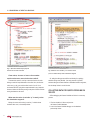
1
Verification Academy
module: “Acceleration
of SystemVerilog
Testbenches with
Co-Emulation”...page 6
A publication of mentor graphics FEB 2011—Volume 7, ISSUE 1
Add the power of emulation to your
existing verification methodology.....
more
Towards Transforming
Verification for the Better
By Tom Fitzpatrick, Editor
and Verification Technologist
Hardware-Assisted Acceleration
of OVM and UVM Testbenches...
the scope of the problem, requirements for
a viable solution, and how to partition your
design and verification hierarchy. page 8
Unique Combo Improves Embedded
Software Integration...we stay in the
emulation world but transform the debug
environment into a software developer’s
dream using Questa ® Codelink. page 14
Accellera UVM1.0 standard... trans-
form verification methodology with some new
capabilities to your toolbox. page 19
Flawless UVM Testbench Creation
...Combining templates and UVM-aware code
entry gets you up and running quickly. page
23
“Boot Camp” training class... finding
qualified verification engineers. page 28
Accelerate Debug of Asynchronous
SystemVerilog Designs... take
advantage of Questa’s transaction recording
API, along with Tiempo’s asynchronous
channel library. page 31
Developing and Deploying OVM
Compliant VIP... useful whether you’re
currently using OVM or plan to move to UVM
in the near future. page 38
The Phase Locked Loop... how to
capture in Verilog this, the most elusive of
all HDL creatures. page 43
Document Driven Verification...
transform your verification planning exercise
into a series of manageable steps. page 46
Hi everyone, and welcome back to Verification
Horizons. For those of you receiving the issue at
DVCon 2011, welcome to the conference! For the rest
of you, you should really plan to attend DVCon next
year. I promise you’ll get a lot out of it and I always
like to meet fellow verification enthusiasts in person.
Here in New England, aside from being hit by yet
another snowstorm (bringing our season total to over five feet and rising), we’re also dealing
with New England Patriots’ playoff loss. So, while
we’re snowed in with nothing else to distract us,
“I was thinking
the attention around here naturally falls once
again to our beloved Red Sox.
about this idea
There’s quite a sense of optimism this year (isn’t
there always?) because the Red Sox have acquired
two very good players for the upcoming season.
Carl Crawford will make the team faster than it has
ever been, especially with Jacoby Ellsbury (one of
my son’s favorites) healthy again after missing most
of last season. Also, Adrian Gonzalez will add some
power that we’ve missed the past year or so. The
transformation of the team should be pretty fun to
watch as the season progresses.
of transformation —
taking something
familiar and adding
a new twist that
makes it better...”
—Tom Fitzpatrick
I was thinking about this idea of transformation—taking something familiar and adding
a new twist that makes it better—as I was reviewing the articles we’re pleased to bring you
in this issue. Just as the Red Sox will still be playing baseball, but playing much better (I hope),
we verification engineers need to transform the way we do verification. I think you’ll find some
helpful tips in this issue.
The first transformation we’ll talk about is adding the power of emulation to your existing
verification methodology. In our first article, my good friend Harry Foster introduces you to our
newest Verification Academy module, “Acceleration of SystemVerilog Testbenches with CoEmulation.” Stay tuned for more of Harry’s insights into the industry this year.
On a related note, my friend Hans van der Schoot and his colleagues in Mentor Graphics’
Emulation Division take us on a detailed walkthrough of “A Methodology for Hardware-Assisted
Acceleration of OVM and UVM Testbenches.” In part one of the twopart series, which forms the basis for the Verification Academy module
described by Harry, you’ll get a good feel for the scope of the problem,
the requirements for a viable solution, and how to partition your
design and verification hierarchy to take advantage of this powerful
technology. In the DAC 2011 issue, we’ll see how to actually implement
the transaction-level interface between simulation and emulation that
lets us take advantage of the emulation performance using our familiar
transaction-based verification environment.
In the next article, “Improving Embedded Software Integration with
Veloce Emulation and the Questa Codelink Debug Environment,”
we stay in the emulation world but transform the debug environment
into a software developer’s dream using Questa Codelink. Using the
same TestBench Xpress (TBX) technology described by Hans, Veloce
can dump out all the information needed to let Codelink display the
software view of the processor(s) in your model, alongside all the other
standard design and testbench debug you need to do.
Next we turn to the standards world where some of us have been
diligently working to complete the Accellera UVM1.0 standard (which is
out for ballot as I write this). By officially adopting the Open Verification
Methodology (OVM) as its foundation, the UVM will transform
verification methodology by adding some new capabilities to your
verification toolbox and becoming the first industry-wide verification
methodology to be adopted as a standard. Mark Glasser gives us an
overview of these capabilities, and commentary on the collaborative
effort by many companies and individuals in this standardization
process, in the “UVM Update” article.
As verification engineers, we’ve all faced the daunting task of
transforming that blank screen (remember when it used to be a
piece of paper?) into a useful testbench. Our next article, “Achieving
Flawless UVM Testbench Creation,” shows how Mentor’s Certe™
Testbench Studio tool can help you do just that. Combining templates
and UVM-aware code entry, Certe gets you up and running quickly. It
also lets you auto-generate register code for your design and look at
the whole thing as a block diagram or UML.
We open our Partners’ Corner in this issue with an account of a
recent “Boot Camp” training class delivered in India by our friends at
DKOP Ltd. All of you managers out there who think it’s too hard to find
qualified verification engineers might want to take a look.
2
Asynchronous designs are always tricky, but in our next article, our
partners at Tiempo explain “How Transaction Viewing Accelerates
Debug of Asynchronous SystemVerilog Designs.” Starting with a
high-level synthesizable design of an asynchronous circuit, the article
shows you how to take advantage of Questa’s transaction recording
API, along with Tiempo’s asynchronous channel library, to make
debugging a snap.
Next, our friends at Test and Verification Solutions share with you
some “Lessons in Developing and Deploying OVM Compliant VIP”
that they learned working on a recent project. These lessons should
prove useful to you, whether you’re currently using OVM or plan to
move to UVM in the near future. And last but not least, my new friend
Mohammed at Vericon, an independent verification consulting firm,
shares with you how to capture in Verilog that most elusive of all HDL
creatures, the Phase Locked Loop.
We close this issue with our Consultants’ Corner, in which our own
Peet James shares his vision of Document Driven Verification, a
process which can transform your verification planning exercise into a
series of manageable steps. Peet’s been doing this a long time and I
think you’ll find his advice both practical and extremely useful.
So, just as we here in Boston hope the Red Sox’s offseason
acquisitions will transform them into a championship team this
year, we at Mentor hope the information you’ll acquire in this issue
of Verification Horizons will help transform your verification team
into champions too. If you’re at DVCon, be sure to visit the Mentor
Graphics booth to find out more, or just stop by to say “hi.”.
Respectfully submitted,
Tom Fitzpatrick
Editor, Verification Horizons
Hear from
the Verification
Horizons team
weekly online at,
VerificationHorizonsBlog.com
3
Table of Contents
Page 6
SystemVerilog Testbench Acceleration
with Co-Emulation
by Harry Foster, Chief Verification Scientist, Design Verification Technology,
Mentor Graphics Corporation
Page 8
A Methodology for Hardware-Assisted
Acceleration of OVM and UVM Testbenches
by Hans van der Schoot, Anoop Saha, Ankit Garg, Krishnamurthy Suresh,
Emulation Division, Mentor Graphics Corporation
Page 14
Improving Embedded Software Integration
with Veloce Emulation and the Questa
Codelink Debug Environment
by Tomasz Piekarz, Technical Marketing Engineer, Mentor Graphics and Joe Rodriguez,
Technical Marketing Engineering Manager, Mentor Graphics Corporation
Page 19
UVM:The Next Generation
in Verification Methodology
by Mark Glasser, Methodology Architect
Page 23
Achieving Flawless UVM Testbench Creation
by Tom Dewey, Technical Marketing Engineer, Mentor Graphics Corporation
4
Partners’ Corner
Page 28
Verification Horizons is a publication
of Mentor Graphics Corporation,
all rights reserved.
by Manu Lauria, DKOP Labs Pvt. Ltd.
Editor: Tom Fitzpatrick
Program Manager: Rebecca Granquist
SystemVerilog Boot Camp
Page 31
How Transactions Viewing
Accelerates Debug of Asynchronous
SystemVerilog Designs
Wilsonville Worldwide Headquarters
8005 SW Boeckman Rd.
Wilsonville, OR 97070-7777
Phone: 503-685-7000
by Nicolas Leblond, Tiempo
To subscribe visit:
www.mentor.com/horizons
Page 38
To view our blog visit:
VERIFICATIONHORIZONSBLOG.COM
Lessons in Developing and Deploying
OVM Compliant VIP
by Mike Bartley, Test and Verification Solutions
and Andy Bond, Lead Verification Engineer, Icera
Page 43
A Full Function Verilog
PLL Logic Model
by Mohammad Ashraf, VeriCon
Consultant’s Corner
Page 46
Document Driven Verification (DDV):
Ready to Throw Out Your Verification Plan?
by Peet James, Mentor Graphics Consulting
5
SystemVerilog Testbench Acceleration with Co-Emulation
by Harry Foster, Chief Verification Scientist, Design Verification Technology, Mentor Graphics Corporation
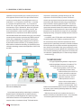
What’s driving today’s SoC design complexity? It’s today’s
consumer demand for devices that handle more and more content—
that include integrated digital, audio, and data—always on and
connected—anytime, anywhere. In fact, today we are seeing that
78% of all new designs fall under the SoC category—containing
multiple embedded processors, lots of internal and external IP reuse,
and embedded software. Verification and validation of these devices,
by nature, is complex.
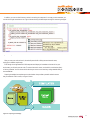
Figure 1 illustrates the typical development and verification/
validation phases for today’s SoC designs. The left-hand column
represents the various development phases, while the bottom
represents various targeted platforms used in the verification/validation
phases. The orange color highlights (in general) the preferred
verification/validation platform for each of the development phases.
As design teams move from the HW IP Development verification
phase into the full SoC Integration verification phase (shown in
Figure 1), performance becomes a critical issue. For example, let’s
consider an SoC that is specifically targeted at a video application.
During the SoC Integration verification and system validation phases,
the verification team will need to verify that the SoC can properly
handle a full frame of video data—ideally in a matter of minutes
versus waiting for days of simulation to complete. Hardware-assisted
speedup in testbench execution becomes compelling under these
circumstances. However, acceleration becomes even more compelling
when it is accomplished without sacrificing other important aspects
and techniques of a comprehensive functional verification flow,
such as coverage-driven, constrained-random, and assertion-based
verification techniques.
This month, to help understand how to
effectively scale verification performance from
the HW IP Development phase through the SoC
Integration and system validation phases, we are
releasing a new Verification Academy module
titled: Acceleration of SystemVerilog Testbenches
with Co-Emulation. In this module, Dr. Hans van
der Schoot demonstrates how to construct a
SystemVerilog transaction-level testbench that
works interchangeably between simulation and
acceleration.
Figure 1. SoC Development and Verification Phases
The new Acceleration of SystemVerilog
Testbenches with Co-Emulation module consists
of 1 hour of content, and it is divided into four
sessions ranging from 7 to 25 minutes in length.
The module should be of general interest;
however, it is particularly targeted at design and verification engineers.
Managers will also find this module interesting.
In releasing the Acceleration of SystemVerilog Testbenches with
Co-Emulation module, our goal is to raise your skill level to the
point where you have sufficient confidence in your own technical
understanding. In turn, this confidence will position you to start the
process of adopting advanced functional verification techniques.
6
As shown in Table 1, the Verification Academy covers a wide variety
of topics, which enables you to start evolving your advanced functional
verification skills.
Table 1. Verification Academy Modules
Module Name
Description
Evolving Capabilities
This module provides a framework for all the modules within the Verification Academy,
while introducing a tool for assessing and improving an organization’s advanced
functional verification capability
Assertion-Based Verification
This module provides a comprehensive introduction to ABV techniques, include an
introduction to SystemVerilog Assertions
CDC Verification
This module provides an understanding of the clock-domain crossing problem, in
terms of metastability and reconvergence, and then introduces verification solutions
FPGA Verification
This module, although targeted at FPGA engineers, provides an excellent introduction
to anyone interested in learning various functional verification techniques
Basic OVM
This module provides a step-by-step introduction to the basics of OVM
Advanced OVM
This module provides the next level of understanding beyond the skills introduced in
the Basic OVM module
Verification Planning
The aim of this module is to define terms, logically divide up the verification effort, and
lay the foundation for actual verification planning and management on a real project
SystemVerilog Testbenches
Acceleration
This module demonstrate how to create a modern testbenches that pairs with coemulation to emable verification productivity improvements in terms of raw performance
I would like to encourage you to check out all our new
and existing content at the Verification Academy by visiting
www.verificationacademy.com.
7
A Methodology for Hardware-Assisted Acceleration
of OVM and UVM Testbenches
by Hans van der Schoot, Anoop Saha, Ankit Garg, Krishnamurthy Suresh, Emulation Division, Mentor Graphics Corporation
Editor’s Note: This is part 1 of a two-part article on this topic.
Part 2 will appear in the DAC edition of Verification Horizons.
This article should serve as a great companion piece to the new
Verification Academy module, Acceleration of SystemVerilog
Testbenches with Co-Emulation.
A methodology is presented for writing modern SystemVerilog
testbenches that can be used not only for software simulation,
but especially for hardware-assisted acceleration. The methodology
is founded on a transaction-based co-emulation approach and
enables truly single source, fully IEEE 1800 SystemVerilog compliant,
transaction-level testbenches that work for both simulation and
acceleration. Substantial run-time improvements are possible in
acceleration mode and without sacrificing simulator verification
capabilities and integrations including SystemVerilog coverage-driven,
constrained-random and assertion-based techniques as well as
prevalent verification methodologies like OVM or UVM.
INTRODUCTION
This article describes a methodology for writing modern
SystemVerilog testbenches that can be used not only for software
simulation, but especially for hardware-assisted acceleration.
Hardware-assisted speedup in testbench execution is compelling
when one considers that ever growing verification complexity, coupled
with short time to market windows and scarce engineering resources,
makes the need for fast simulation run times increasingly critical. For
instance, think of viewing a full frame of graphics in a matter of minutes
instead of a day of simulation. Simply put, faster testbenches enable
longer and more test cases to be run in less time, allowing more
requirements to be covered and more bugs uncovered.
Hardware-assisted testbench acceleration can in principle be
achieved with full emulation through a fully synthesizable testbench, or
more conventionally with co-simulation where an RTL DUT is mapped
onto an emulation platform that interacts with the simulated testbench
on a workstation at a clock cycle basis. With today’s advanced
transaction-level testbenches, however, the pragmatic approach is to
have certain testbench components – the lower pin-level components
8
like drivers, monitors etc. – synthesized into real hardware and
running inside the emulator together with the DUT, while other nonsynthesizable testbench components – the higher transaction-level
components like generators, scoreboards, coverage collectors etc.
– remain in software running inside the simulator. Communication
between simulator and emulator is consequently transaction-based,
not cycle-based, reducing communication overhead and increasing
performance because data exchange is infrequent and informationrich and high frequency pin activity is confined to run at full emulator
clock rates.
The methodology presented herein promotes this so-called
co-emulation (also known as co-modeling) approach and aims to
maximize reuse between pure simulation-based verification and
hardware-assisted acceleration. It enables truly single source, fully
IEEE 1800 SystemVerilog compliant, transaction-level testbenches
that work interchangeably for both simulation and acceleration.
In acceleration mode it offers substantial run-time improvements
while retaining all simulator verification capabilities and integrations.
This includes in particular support for modern coverage-driven,
constrained-random and assertion-based techniques in SystemVerilog
as well as prevalent verification methodologies like OVM or UVM, and
VMM. The subsequent sections lay out the details of and illustrate
the proposed transaction-based acceleration methodology for
SystemVerilog in terms of the testbench architecture and modeling
rules and guidelines.
TERMINOLOGY
Co-emulation, or (transaction-level) co-modeling, is the process of
modeling and simulating untimed behavioral models in conjunction
with synthesizable hardware models running on an emulator,
intercommunicating through transactions or function/task calls. The
untimed transaction-based behavioral models are collectively referred
to as the HVL side, while the cycle-accurate synthesizable hardware
models constitute the HDL side.
SCE-MI 2, or Standard Co-Emulation Modeling Interface 2, is a
set of standard modeling interfaces defined within Accellera for multichannel communication between software models describing system
behavior (i.e. the HVL side) and structural models describing the
implementation of a hardware design (i.e. the HDL side). It is based
on SystemVerilog-DPI as the foundation to realize communication
between HDL code running in an emulator and C/C+/SystemC code
running on a workstation.
A transactor is a component responsible for converting untimed
transactions into a series of cycle-accurate clocked events to be
applied to a given pin interface, and/or conversely, for converting
cycle-accurate pin activity observed into higher level transactions. In
the specific context of hardware-assisted verification, a transactor is a
SystemVerilog interface or module on the HDL side that has a signallevel interface to the DUT and a transaction-level interface to the HVL
testbench. Transactors are sometimes also referred to as BFMs (Bus
Functional Models) and the two terms are henceforth considered
synonymous.
TBXTM, or TestBench XpressTM, is the third generation hardwareassisted acceleration solution from Mentor Graphics, enabling
state-of-the-art, comprehensive transaction-based co-emulation
coupled to Mentor Graphics’ Veloce emulation
platform. It includes synthesis support of a rich
extension of the RTL subset of SystemVerilog
with behavioral clock generation and reset
logic, initial and final blocks, implicit FSMs,
SystemVerilog-DPI functions and tasks,
synchronization events, waits, system tasks
and more, thereby offering maximum HDL
modeling flexibility without performance
penalties.
accurate signal level of abstraction near the DUT and the transaction
level of abstraction in the rest of the testbench. A co-emulation
flow enforces this separation and requires that the transactor layer
components are included on the HDL side to run alongside the DUT
on the emulator. It further requires that the HDL and HVL sides are
completely separated hierarchies with no cross module or signal
references, and with the code on the HVL side strictly untimed.
This means that the HVL side cannot include any explicit time
advance statements like clock synchronizations, # delays and wait
statements, which may occur only on the HDL side. Abstract event
synchronizations and waits for abstract events are permitted on the
untimed HVL side, and it is still time aware in the sense that the current
time as communicated with every context switch from HDL to HVL side
can be read. As a result of the HDL-HVL partitioning, performance
can be maximized because testbench and communication overhead
is reduced and all intensive pin wiggling takes place in the grey area in
Figure 1 targeted to run at emulation speeds.
REQUIREMENTS
Several requirements are at play when
devising a transaction-based acceleration
methodology for SystemVerilog. Firstly, it must
adhere to the principles of co-emulation which
implies the need to partition a testbench into a synthesizable HDL
side and a distinct HVL side handled by separate tools running on two
different physical devices – emulator and workstation – and interacting
at the transaction-level. The HDL side, then, must bear the limitations
of modern day synthesis technology, and the communication with the
HVL side must be fast and efficient so as to minimize impact on raw
emulator performance.
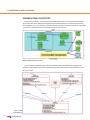
Today’s transaction-based testbenches like OVM/UVM testbenches
have a layered foundation that exhibits a separation between timed
and untimed (or partially timed) aspects of the testbench. As illustrated
in Figure 1, a transactor layer forms the bridge between the cycle-
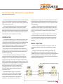
Figure 1. Transaction-based testbench
Another important methodology requirement is that it yields ‘singlesource’ testbenches for both simulation and acceleration. This means
that the HVL-HDL partitioning must function the same in co-emulation
and in simulation alone, yet without the use of hooks like compile-time
or run-time switches that would disable entire branches of code and
pretty well implement two separate code bases. It also implies that the
benefits of using SystemVerilog and verification methodologies like
OVM or UVM for creating modular, reusable verification components
and testbenches must be preserved along with associated simulator
9
capabilities for analysis and debug. Key to achieving that proves to
be the application of what is known in the object oriented world as
a remote proxy design pattern. In this design pattern access to a
remote object – e.g. a component on the HDL side – is controlled
by a surrogate in the application domain – e.g. a component on
the HVL side – through some indirect reference to uniquely access
the remote object. Figure 2 illustrates this, where driver, responder
and monitor components in blue act as proxies on the HVL side
for the real transactors in yellow on the HDL side implementing
synthesizable driver, responder and monitor BFMs, respectively.
Communication between each transactor and its proxy occurs through
a remote procedure invocation mechanism using BFM-like task and
function calls, as detailed later. The mechanism is inspired by the
known Accellera SCE-MI 2 function model and has the same kind
of performance benefits as SCE-MI 2 [1]. This modeling practice in
effect enables an acceleration methodology for SystemVerilog that is
verification methodology neutral and thus applicable to OVM or UVM,
and VMM.
components in SystemVerilog, optionally derived from the TLM
components in the OVM class library. It provides TLM fifos and
channels, ports and exports that are enhanced for message passing
across the HVL-HDL abstraction boundary using an intermediate C
layer and SCE-MI 2 compliant SystemVerilog DPI-C. The rationale
was that with the Accellera SCE-MI 2 standard already defining the
communication semantics between HDL transactors and C models [1],
XTLM implements an extra layer above the C layer to make the latter
transparent to the user. Because of its usage of C as an intermediate
language layer though, this approach naturally inherits the restrictions
of that language.
In comparison, where XTLM enables a set of fabricated HVL-HDL
connections built from the XTLM library components with a fixed
API, the transaction transport mechanism presented here utilizes
exclusively built-in SystemVerilog constructs for a flexible user-defined
API that is simpler and more intuitive and therefore generally easier to
learn. And with the intermediate C layer gone, it proposes just a small
structural change at the boundary between DUT and testbench as part
of the verification methodology used, where XTLM is structurally much
more obtrusive. A detailed description of XTLM and usage examples
can be found in [5].
THE METHODOLOGY
Figure 2. Transaction-based testbench
with transactor/BFM proxies
A prior attempt towards enabling a methodology for accelerating
SystemVerilog and OVM testbenches was made by Saha et al.
in [5], proposing a considerably different use model for HVL-HDL
communication referred to as XTLM (eXtended TLM). XTLM
comprises a library of ‘acceleration-friendly’ TLM-based interface
10
For a typical SystemVerilog testbench a single top level
module encapsulates all elements of the testbench. This
includes all verification environment components,
clock and reset generators, the RTL DUT, and
any SystemVerilog interfaces used to
bundle the external pins of the DUT for
access by environment components.
In the common case of class-based
verification components, such as
OVM components, the access to
the pins to drive or sample values is
through a virtual interface handle – a
pointer to a concrete interface. Virtual
interfaces are the established means to connect an OVM testbench or
any dynamic, object-oriented SystemVerilog testbench to a statically
elaborated HDL model.
While this practice works fine for simulation it falls short for coemulation, demanding two separated hierarchies – one synthesizable
– that transact together without direct cross signal accesses.
A methodology that does meet the requirements for co-emulation can
be defined in terms of three high level steps as follows:
1. Employ two distinct HVL and HDL top level module hierarchies;
2. Identify the timed testbench portions and model for synthesis
under the HDL top level hierarchy;
3. Implement a transaction-level interface between the
HVL and HDL top level hierarchies.
The next sections describe each of these steps in detail.
Creating Two Distinct HVL
And HDL Top Level Module Hierarchies
As the conventional single top testbench architecture is not suited
for co-emulation, the first step is to rearrange and create dual HVL
and HDL top level module hierarchies. This is conceptually quite
simple, as shown in Figure 3. The HDL side must be synthesizable
and should contain essentially all clock synchronous code, namely the
RTL DUT, clock and reset generators, and the BFM code for driving
and sampling DUT interface signals. The HVL side should contain all
other (untimed) testbench code including the various transaction-level
testbench generation and analysis components and proxies for the
HDL transactors.
This modeling paradigm is facilitated by virtue of advancements
made in synthesis technology across multiple tools. For example,
Mentor Graphics’ TBXTM provides technology that can synthesize not
only SystemVerilog RTL but also implicit FSMs, initial and final blocks,
named events and wait statements, import and export DPI-C functions
and tasks, system tasks, memory arrays, behavioral clock and reset
specification along with variable clock delays, assertions, and more.
All supported constructs can be mapped on a hardware accelerator,
and all models synthesized with TBXTM run at full emulator clock rate
for high performance. Moreover, they can be simulated natively on
any IEEE 1800 SystemVerilog compliant simulator. This synthesis
advancement was a precursor to the SCE-MI 2 standard developed
within Accellera to enable effective development
of ‘emulation-friendly’ transactors [1].
Figure 4 on the following page illustrates
the rearrangement of a conventional single top
hierarchy (module top in Figure 4.a) into a dual
HDL-HVL top hierarchy (modules hdl_top and
hvl_top in Figure 4.b) for co-emulation. This code
example and subsequent code examples are
based on a SystemVerilog testbench for a floating
point unit (FPU) design adopted from the OVM
cookbook [2]. As one can see, the FPU design
and pin interface have moved to the HDL top level
module (i.e. lines 10-17 and 12-19 in Figure 4.a.
and 4.b), together with the clock generator (i.e.
lines 26-33 and 21-25 in Figure 4.a. and 4.b).
The clock generator has changed slightly with
the use of a specific initial block in place of the
non-synthesizable fork-join block.
Figure 3. Separated HVL and
HDL top level module hierarchies
11
1
2
3
4
5
6
7
8
9
10
11
12
13
14
15
16
17
18
19
20
21
22
23
24
25
26
27
28
29
30
31
32
33
34
35
36
37
38
module top;
parameter int HALF_PERIOD = 12;
parameter int DATA_SIZE = 8;
parameter int ADDR_SIZE = 10;
env #(DATA_SIZE, ADDR_SIZE) e;
fpu_vif fpu_vif_obj;
bit clk;
fpu_pin_if #(32) fpu_if (clk);
fpu fpu_dut(fpu_if.clk,
fpu_if.opa,
...,
fpu_if.snan
);
initial begin
e = new(“env”);
fpu_vif_obj = new(fpu_if);
set_config_object(
“*”, “fpu_vif”, fpu_vif_obj, 0);
// start the clock running
clk = 0;
fork
forever begin
#HALF_PERIOD;
clk = !clk;
end
join_none
run_test();
end
endmodule
(a) Single top hierarchy
1 package test_params_pkg;
2
parameter int HALF_PERIOD = 12;
3
parameter int DATA_SIZE = 8;
4
parameter int ADDR_SIZE = 10;
5 endpackage
6
7
8 module hdl_top;
9
10
import test_params_pkg::*;
11
12
bit clk;
13
fpu_pin_if #(32) fpu_if (clk);
14
15
fpu fpu_dut(fpu_if.clk,
16
fpu_if.opa,
17
...,
18
fpu_if.snan
19
);
20
21
// tbx clkgen
22
initial begin // Clock generator
23
clk = 0;
24
forever #(HALF_PERIOD) clk = ~clk;
25
end
26
27 endmodule
28
29
30 module hvl_top;
31
32 import test_params_pkg::*;
33
34 env #(DATA_SIZE, ADDR_SIZE) e;
35 fpu_vif fpu_vif_obj;
36
37 initial begin
38
e = new(“env”);
39
40
fpu_vif_obj = new(hdl_top.fpu_if);
41
set_config_object(
42
“*”, “fpu_vif”, fpu_vif_obj, 0);
43
44
run_test();
45 end
46
47 endmodule
(b) Dual top hierarchy
Figure 4. From conventional single top to dual top hierarchy for co-emulation
12
A common package has also been introduced for convenient
sharing of test parameters between the separate HDL and HVL top
level hierarchies (i.e. lines 3-5 and 1-5, 10, 32 in Figure 4.a. and 4.b).
The remainder of the single top hierarchy has been preserved under
the HVL top level module including a virtual pin interface connection,
now by hierarchical cross reference hdl_top.fpu_if into the HDL top
level module (i.e. line 40 in Figure 4.b). Certainly, neither a pin-level
HVL-HDL interface nor an HVL-HDL cross module reference is
permitted in the dual top co-emulation architecture, but this will be
remedied in the next step where each transactor layer component is
split into a synthesizable BFM on the HDL side and a corresponding
untimed testbench component on the HVL side using a purely
transaction-based communication mechanism.
It is worth pointing out that, besides hardware-assisted acceleration,
there are other good reasons to adopt a dual top testbench
architecture. For instance, it can facilitate the use of multi-processor
platforms for simulation, the use of compile and run-time optimization
techniques, or the application of good software engineering practices
for the creation of highly portable, configurable VIP as discussed in [3].
Modeling The Timed Testbench
Under The HDL Top Level Module
Forming the abstraction bridge between the timed signal level and
untimed transaction level of abstraction, transactor layer testbench
components like drivers, monitors or responders convert ‘what is
being transferred’ into ‘how it must be transferred’, or vice versa, in
accordance with a given interface protocol. The timed portion of such
a component is reminiscent of a conventional BFM, a collection of
threads and associated tasks and functions for the (sole) purpose
of translating to and from timed pin-level activity on the DUT.
In SystemVerilog object-oriented testbenches this is commonly
modeled inside classes, e.g. classes derived from the ovm_driver or
ovm_monitor base classes in OVM. The DUT pins are bundled inside
SystemVerilog interfaces and accessed directly from within these
classes using the virtual interface construct. Virtual interfaces thus
act as the link between the dynamic object-oriented testbench and the
static SystemVerilog module hierarchy.
for example a transaction-level interface to upstream components in
the testbench layer. All BFMs must therefore be ‘surgically’ extracted
and modeled instead as synthesizable SystemVerilog HDL modules or
interfaces.
Using this principle it is possible without much difficulty to
write powerful state machines to implement synthesizable BFMs.
Furthermore, when modeling these BFMs as SystemVerilog
interfaces it is possible to continue to utilize virtual interfaces to
bind the dynamic HVL and static HDL sides. The key difference with
conventional SystemVerilog object-oriented testbenches is that the
BFMs have moved from the HVL to the HDL side and the HVL-HDL
connection must now be a transaction-level link between testbench
objects and BFM interfaces. That is, testbench objects may no longer
access signals in an interface directly, but only indirectly by calling
(transaction-level) functions and tasks declared inside a BFM interface.
This yields the testbench architecture already discussed briefly in
Section 2 and depicted in Figure 2. It works natively in simulation and
it has been demonstrated to work also in co-emulation (i.e. with Mentor
Graphics’ Veloce TBXTM acceleration solution). The next article will
detail the concrete mechanism for HVL-HDL communication using
remote function/task calls.
REFERENCES
[1] Accellera – Interfaces Technical Committee, “Standard CoEmulation Modeling Interface (SCE-MI) Reference Manual,” Version
2.1 (Review Copy), October 21, 2010
[2]
M. Glasser, “Open Verification Methodology Cookbook,”
Springer, 2009. (Associated example kit available at www.ovmworld.
org/contribution-detail/24891)
[3]
A. Rose, M. Glasser, B. Osman, “OVM Configuration and
Virtual Interfaces,” White Paper, Mentor Graphics, 2010.
[4]
H. van der Schoot, J. Bergeron, “Transaction-Level
Functional Coverage in SystemVerilog,” DVCon, 2006.
[5]
A. Saha, K. Suresh, A. Jain, V. Kulshrestha, S. Gupta, “An
Acceleratable OVM Methodology Based on SCE-MI 2,” DVCon, 2008.
With regard to co-emulation, BFMs are naturally timed and must
be part of the HDL top level module hierarchy, while dynamic class
objects are generally not synthesizable and must be part of the HVL
hierarchy. In addition, a transactor layer component usually has some
high level code next to its BFM portion that is not synthesizable either,
13
Improving Embedded Software Integration with Veloce
Emulation and the Questa Codelink Debug Environment
by Tomasz Piekarz, Technical Marketing Engineer, Mentor Graphics and Joe Rodriguez,
Technical Marketing Engineering Manager, Mentor Graphics Corporation
Today’s system-on-chip (SoC) designs are increasingly dependent
on firmware and device drivers. Accordingly, leading semiconductor
companies are looking to more closely integrate software development
and validation with silicon design and verification. One obstacle to
such integration addressed in this article, is the difficulty in effectively
debugging early-stage embedded software. What follows is a
description of a new software debugging methodology for software
and system-level integration teams called Questa Codelink. When tied
with Mentor Graphics Veloce hardware emulation platform, Questa
Codelink reduces debug closure time and effort required to develop
SoC firmware and device drivers.
Debugging software when using Veloce
Emulation has a solid performance record. Its clock speed is
generally high enough to boot an OS and then load and execute
application-level software from a flash card. Emulators experience
little performance dropoff even as the design grows. For this reason,
at both the early and late stage of development, emulation can make
sense for debugging embedded software.
Of course there is a catch. Today it’s possible to attach a software
debugger via JTAG or parallel interfaces to the processor running in
Veloce. While these methods work, it can be impractical for embedded
software teams to allocate time on Veloce which is often a highly
utilized resource in a development flow. Throughout the duration of
many projects, the emulation queue is mostly full with batch jobs
scheduled to run more or less continuously. Questa Codelink now
makes it easier to add software-related batch jobs to this queue and
then debug the results later offline.
Imagine you are developing software for printing a scanned picture.
The workflow of the imagined end user is to boot up the operating
system, configure the hardware, and scan and ready the picture for
printing. Debugging this workflow takes time. Depending on the size
of the operating system, booting the design may take anywhere from
minutes to hours. A typical process of getting to the problematic
14
portion of the software might be to set the breakpoint and run
simulation, start and configure the design until hitting that breakpoint,
and then start debugging from there. Getting to the breakpoint may
take time. Also, debugging usually is not done in one run since it
takes multiple iterations to focus in on the problem. Nothing is more
frustrating during debugging than being almost there, almost able to
see the problem, but ultimately making one step too many and having
to start all over again.
Let’s imagine that it takes 20 minutes for the print/scan software
example to run on the emulator, but it takes four hours to debug and
fix the problem. If debug could be taken off Veloce and done offline,
then during the four hours spent diagnosing the problem, 12 other runs
could be performed on the emulator or 12 other engineers could have
access to the emulator. Now with Questa Codelink, offline debug is a
reality.
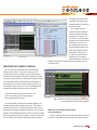
Improving software debug with Questa
Codelink and Veloce
The combination of Questa Codelink and Veloce creates a debug
environment that connects to the database generated from the
CPU code execution during the emulation run. Given the emulator’s
speed, it’s entirely possible you’ll be looking at a large amount of
source code. (Think here of booting an OS.) It is important to have an
environment that allows you to quickly pan through large swathes of
code and identify where you want to look deeper. The Questa Codelink
debugger allows for stepping through the design forward or backwards
at the high level source or the assembly level. The debugger displays
the CPU registers as well as variables, memory contents and call
stack view. It is fully synchronized with the hardware environment by
connecting to the cursor in the waveform window. Stepping forward or
backward updates all other displays in the debugger and moves the
cursor in the waveform to the correct time when the data was sampled
during the run. (The inverse holds true as well: by moving the cursor in
the waveform, all the debugger views will update accordingly.)
is triggered to see what caused
it. But again, from looking at the
hardware waveform, how does he
know when to stop?
Fig. 1: Questa Codelink debug environment.
Now, imagine you’re the
engineer and you’ll use Questa
Codelink to help with debugging
this problem. For starters, you
don’t have to re-run the emulation
because the tool already gathered
all the data you need. You can
start debugging the output from
Veloce right away, starting at the
failure and methodically moving
backwards to find the cause.
You also won’t have to work on
Veloce since you can debug
offline. Guiding your work are four
questions and answers to which will lead you to the state of the CPU
just before it failed:
Debugging with Questa Codelink
Let’s look at how this environment can be used to debug a
relatively common failure. The processor is executing code
normally and then there is a problem in communication between
the software and the hardware in the design. Perhaps the software
was trying to get data from the un-initialized ASIC register and read
a corrupted value. When the software tries to perform some ALU
operation based on this value, it freezes, producing a “flat line” in
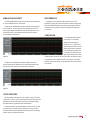
the hardware waveform (see Fig 2). To even start debugging what
happened, the software engineer will have to understand:
1. What was the software doing at the end of the run?
2. What was the last good line of code executed?
3. What caused the CPU to freeze
FIG. 2: Processor “flat lines” at the end of the emulation
run. See the flat lines at the end of waveform.
Let’s assume (hardly a stretch) that the software engineer is not
familiar with the hardware verification environment. This means it is
extremely difficult for him to correlate his software to what he sees
happening in the hardware waveforms. Perhaps he’d opt to re-run the
emulation with the debugger attached to the CPU. However this would
take time (possibly hours to redo the whole run). What he really needs
to do is to stop the CPU execution immediately before the problem
What line of code was last executed
in the simulation?
To find out, move the cursor to the last executed instruction and look
at the source code. Below, that’s line number 135 in demo_diag.c file:
15
Fig. 3: Questa Codelink helps pinpoint
the last line of code executed.
Fig. 4: Mouse over variable “p” to show its value
(zero as shown above) when simulation stopped
From where, in terms of source line number
and function name, was the function called?
To answer this question, scroll up to see what function the code
belongs to and then step backwards to the caller. Here, the function
call is send_to_dbg_port and the caller is main.c line 411. In an
environment like this, being able to step backwards is very important
because it allows for efficiently starting at the place of failure and then
tracing backwards to the cause.
What was the value of variable “p” in main() when
the simulation stopped?
Moving the cursor and hovering it over the “p” variable shows
the latest value: zero, in the example below.
16
So, taking the debug process offline and allowing for replaying
emulation brings many benefits. It not only presents a high level
software debug environment familiar to embedded software engineers,
but also keeps Veloce in use all the time.
Collecting data for Questa Codelink on
Veloce
Offline debugging with Questa Codelink and Veloce is a two-step
process:
1. Run the simulation in Veloce and produce
the Questa Codelink database.
2. Launch the Questa Codelink debugger on the database
produced by Veloce.
Non-intrusiveness is one of Questa Codelink’s main benefits.
Using the the tool with data generated by Veloce doesn’t require any
additional hardware or design changes, thus preserving your system’s
behavior. Properly deployed, the Questa Codeline-Veloce resource
can be a virtual grid resource that is leveraged from anywhere on the
globe. Logging is done through the TBX monitor, which is attached
to the design and compiled into Veloce. This emulated monitor sits
outside the design and observes the pins and CPU register changes
directly inside the CPU.
To maintain emulation speed, the Veloce-generated data is not the
final Questa Codelink database but rather a raw data stream called
Codelink Change List file. This file is later post-processed to create
the final Questa Codelink replay log file that can be used to replay the
emulation run. The final log file taken to the developer’s local machine
is used for debugging, thus freeing up Veloce for other runs.
Multi Core and Multi CPU support
Questa Codelink also provides support for simultaneous logging
of multiple CPUs or cores. In either case, the process is exactly the
same as previously described with one exception: one log file per core
is generated. So if there are two cores being logged in Veloce – a
process that happens simultaneously – then two Questa Codelink
replay files will be generated. This is efficient since the files can
then be analyzed individually. For example, consider an ARM design
with two cores, each of which will run unique software written by a
developer. (That is, a different developer is responsible for each core
and its associated software.) Presumably, each developer would only
be interested in debugging the CPU that he is working on, which the
tools and workflow I’m describing in this article do allow.
Fig. 5: Questa Codelink – collecting data on Veloce.
Once the database is created, it can be
analyzed offline via the Questa Codelink debugger:
Questa Codelink connects to both Questa
and Verdi waveform viewers. So, to see hardware signals
and correlate them to software execution, either use the Verdis
database or convert the VCD file to the Questa wlf format. And
of course if hardware logs are not needed,
then Questa Codelink will not require waveform files
generated by Veloce.
During the debug session, Questa Codelink allows for viewing of
multiple CPUs side by side. Each view is synchronized, which means
that stepping in one core (and waveform window) will adjust the
second core accordingly.
17
Fig. 7 : Questa Codelink supports multi core architecture with
a user interface that provides side-by-side viewing of each core.
Conclusion
Questa Codelink allows for a better, more flexible offline software
debug environment and can increase Veloce throughput. The
approach – logging the CPU activity during simulation in Veloce and
replaying it outside of the emulator – allows for Veloce to be constantly
used for different emulation runs or by different engineers. Questa
Codelink is nonintrusive and doesn’t require design changes. The
tool preserves original design behavior and allows for logging and
debugging multi-core and multi-CPU designs in one user-friendly
environment. It also can be used for debugging RTL in the logic
simulator, thus extending the same debug environment across
different verification boundaries.
18
UVM:The Next Generation in Verification Methodology
by Mark Glasser, Methodology Architect
UVM is a new verification methodology that was developed by the
verification community for the verification community. UVM represents
the latest advancements in verification technology and is designed to
enable creation of robust, reusable, interoperable verification IP and
testbench components.
One of the most novel and exciting aspects of UVM is how it was
developed. Rather than being developed by a single EDA vendor
and rolled out as part of a marketing campaign, it was developed by a
collection of industry experts representing microprocessor companies,
networking companies, verification consultants, as well as EDA
vendors. All the work was done under the auspices of Accellera.
Within the umbrella of a standards organization, companies, some
of whom compete with each other in the market place, were able to
come together in a collaborative environment to address the technical
challenges of building a sophisticated verification methodology.
Each representative brought in expertise and perspectives from their
segment of the industry. The result is a powerful, multi-dimensional
software layer and methodology for building verification environments.
Of course, UVM has been tested on all simulators of the major EDA
vendors. UVM is truly an industry initiative, one in which Mentor is
proud to participate.
UVM was not built from scratch. It is the culmination of many
independent efforts in the verification methodology space.
Its heritage includes AVM, URM, VMM, and OVM.
These previous methodology libraries provide a rich legacy upon
which UVM is built. Most notably, OVM-2.1.1 was the “starting point”
for UVM, the code base that seeded the development effort.
As a result, UVM most closely resembles OVM, and is largely
backward compatible with OVM. The RAL package that was
part of VMM was transformed into the register facility in UVM.
While these methodologies were the seed from which UVM
grew, the final product is not simply a conglomeration of code
drawn from its predecessors. UVM moves the
state-of-the-art forward by providing
new facilities and new use models for
testbench construction.
Figure 1: UVM Heritage
Registers
In modern SoC designs, a collection of registers is the interface
to a design. It is through the registers that devices are reset and
configured, and data transmitted and received. Modeling its registers
is critical to verifying the functionality of any device. UVM provides a
comprehensive facility for modeling registers of all types. The facility
includes “back door access”, the ability to access a register in the RTL
through its corresponding UVM model.
To use the register facility you must create a map that contains a set
of registers and the bus address to which each is mapped. A register
sequence uses the map to locate registers and determine their bus
addresses. Register methods such as read() and write() cause a
19
bus transaction to be generated and sent to the sequencer. The bus
transaction contains the addresses of the register gleaned from the
register map.
the shutdown phase and run is also
completed will execution reconverge as
the extract phase starts.
Registers are contained in a structure called a register block.
Register blocks contain not only registers, but also register files and
other register blocks. In this way register blocks can be composed
hierarchically, just as systems are. Registers in sub-blocks are
relocated within the address space of the parent.
It is also possible to jump backwards
to execute a phase again or to
jump forward to skip a phase. This
feature enables you to model resets,
for example or other asynchronous
behavior.
A leaf block, one that doesn’t contain other register blocks,
typically represents a device on a bus – i.e within an address space.
A composite block, one that does contain other register blocks,
represents a system or subsystem. When a block is added to a parent
block the new block’s address are relocated automatically within the
parent’s address space.
Phasing
The execution of a UVM testbench is orchestrated by a centralized
controller. The controller steps the testbench through each of its
phases. UVM enables the construction of complex phasing schemes
that are required to properly stimulate and respond to SoCs. UVM
specifies a collection of base phases that will accommodate a large
segment of SoC design styles. For those segments where the base
set is not sufficient, UVM provides a means for users to add their own
phases and specify their ordering relative to other phases.
A phase is a function or task that executes some portion of the
testbench. You can think of it as a step in testbench execution. The
phasing executive steps through each phase. When all the phases
finish then the testbench execution is complete. As execution
proceeds, each component in the testbench is in the same phase.
When all the tasks or functions finish, then the phasing executive
transitions to the next phase. In this way all of the components stay
synchronized as during testbench execution.
UVM brings some innovation to the phasing mechanism. Instead
of a straight-line ordering of phases, UVM organizes phases as a
directed graph. The graph structure enables phases to be partially
ordered, that is some phases operate together in parallel, while others
operate sequentially. The graph shown on the right is an example.
Most of the phases operate sequentially. Notice that after start-ofsimulation the reset-init-main-shutdown1 branch operates in parallel
with the run phase. When start_of_simulation finishes then both the
reset and run phases are started. The branch on the left operates
independently of the run phase. Only when the left branch completes
1
20
UVM provides a set of built-in phases
that testbench builders can use to
create the steps necessary to execute
their testbench. Additionally, users can
create their own phases to customize a
testbench for their particular purpose.
Resources
Configuring a testbench is a critical
part of its operation. It involves making
pieces of information available to
various testbench elements. UVM
provides a facility called resources that
enables you to configure a testbench
efficiently and elegantly.
A resource is a container that
holds an object of an arbitrary type.
The object can be a bit, an integer,
a class object, a virtual interface, or
anything else. Resources are stored
in a centralized database called
the resource pool. Any object in a
testbench can access the resource
pool to set or get resources.
Each resource has a regular expression that represents the set of
scopes over which it is visible. A regular expression is a shorthand
notation for a set of strings. In this case, those strings are names
of scopes. Scope names are hierarchical names that contain dots
as separators of the hierarchical elements. E.g. top.env.agent has
three elements, top, env, and agent. The regular expression top.env.*
represents all the strings that begin with top.env. This notation refers
to all the scopes that are subordinate to top.env.
Each of these phases also has a pre- and post- phase associated with it (ie. pre_reset, reset, post_reset). These were left off to simplify the diagram.
When an object looks up a resource in the resource pool, it
identifies itself as belonging to a particular scope. This is referred
to as the current scope. The lookup function asks whether or not
a resource that matches all other search criteria also matches the
current scope. If it does then the resource is returned.
Resources are stored both by name and by type. You can store
and retrieve a resource by its name or by its type. Retrieval by type
is useful for cases where you know the type is unique. Consider , for
example, an agent that uses a configuration object and the type of the
configuration object is supplied as a class parameter.
class some_agent #(type CONFIG=int) extends uvm_component;
endclass
The agent can simply retrieve its configuration object from the
resource pool by type, confident that the object whose type is
specified by the CONFIG class parameter is the one it needs.
A name is not necessary in this case.
Since the resource pool is a centralized singleton structure
any testbench element can access it. This includes components,
sequences, or any other element. Sequences, for example
can obtain information from the resource pool to guide their
operation. Register sequences can obtain register maps from
the resource pool.
In TLM-2.0 the mechanism for moving transactions between
components is based on three interfaces:
function uvm_tlm_sync_e nb_transport_fw(T t, ref P p, input uvm_tlm_
time delay);
function uvm_tlm_sync_e nb_transport_bw(T t, ref P p, input uvm_tlm_
time delay);
task b_transport(T t, uvm_tlm_time delay);
nb_transport_fw() and nb_transport_bw() are used for bidirectional
nonblocking communication. the b_transport() task is a blocking
transport, similar to put() or get() in TLM-1.0. An essential difference
between TLM-1.0 and TLM-2.0 is that transaction objects are
passed by reference in TLM-2.-0. This can make for more efficient
communication as less copying of data is required.
These interfaces are contained in sockets, port-like objects that are
used to make connections between components. A socket contains
both the forward and backward path.
Because of the generalized nature of resources, there are
many use models possible. Some of them are described in [1].
TLM2
Transaction-level modeling has long been at the heart of modern
verification methodologies. Keeping as much of the testbench
as possible at a high level of abstraction is important for building
robust and reusable testbench elements. As a step forward toward
improving the transaction-level modeling facilities UVM includes an
implementation of TLM-2.0. TLM-2.0 is a standard methodology
for building and connecting transaction-level components that
was developed by OSCI (Open SystemC Initiative) and will be part
of the IEEE-1666-2011 standard. The UVM implementation is in
SystemVerilog, of course, and includes the essential elements of
the TLM-2.0 standard. A detailed discussion on how TLM-2.0 was
translated from SystemC to SystemVerilog is in [2].
Figure 3: TLM-2.0 Sockets
21
TLM-2.0 supports different kinds of sockets. A socket is an initiator
or a target, a terminator or a passthrough, has blocking or nonblocking
interfaces. This leads to eight different kinds of sockets as listed in the
following table:
blocking-initiator-terminator
nonblocking-initiator-terminator
blocking-target-terminator
nonblocking-target-terminator
blocking-intiator-passthrough
nonblocking-initiator-passthrough
blocking-target-passthrough
nonblocking-target-passthrough
Passthrough sockets are used for making socket connections
across hierarchical boundaries. Terminator can be initiators, which
initiate transactions, or targets, which received transactions and send
responses in the backward path. Blocking sockets use the blocking
interface and may consume time, nonblocking sockets use the
nonblocking interfaces which are functions and do not consume time.
Summary
UVM represents the next generation in verification methodology.
It was created not by a single organization, rather it was built by many
industry organizations working collaboratively. UVM moves the state
of the art forward for verification methodology with new features
such as a sophisticated phasing mechanism, a facility for modeling
registers, a comprehensive configuration facility called resources, and
a SystemVerilog implementation of the new transaction-level modeling
standard, TLM-2.0.
Bibliography
[1] M. Glasser, Advanced Testbench Configuration With Resources,
Proceedings of DVCon 2011
[2] M. Glasser and J. Bergeron, TLM-2.0 in SystemVerilog,
Proceedings of DVCon 2011
[3] M. Glasser, The OVM Cookbook, Springer, 2009
[4] A. Erickson, “Are Macros in OVM and UVM evil?
A Cost Benefit Analysis”, Proceedings of DVCon 2011
[5] G. Allan, “Verification Patterns in the Multicore SoC Domain”,
Proceedings of DVCon 2011
[6] IEEE-1800-2009, SystemVerilog Language Reference Manual,
2009
[7] Accellera, UVM-1.0 Reference Manual, 2011
22
Achieving Flawless UVM Testbench Creation
by Tom Dewey, Technical Marketing Engineer, Mentor Graphics Corporation
Introduction
Capture Knowledge and Get Help
Perhaps you have created many testbenches and it is time to
reflect on how you can improve the creation process based on
your experiences and by adopting the UVM (Universal Verification
Methodology). In order to achieve a flawless UVM testbench, you need
a method to:
Knowledge about creating the ideal testbench can typically be
found in best practices or coding standards documents, golden code
samples, or in an engineer’s head. You can capture all these sources
of information in templates. This allows your testbenches to leverage
collective knowledge and to focus on the code that actually makes
your particular testbench unique.
• Automate as many creation steps as possible
• If automation is not possible, have reliable advice
readily available for every decision point
Mentor Graphics created Certe™ Testbench Studio specifically
to help you create near-perfect testbenches every step of the way
through your UVM testbench project. And, if you are utilizing AVM
(Advanced Verification Methodology) or OVM (Open Verification
Methodology), the tool supports those methodologies as well.
This article shows you how to approach creation perfection
by using Certe Testbench Studio.
Typically, one person creates templates to share across teams and
corporations. This person decides what elements of UVM that are
typically reused in any testbench, such as agents, scoreboards, or
even file headers.
Certe Testbench Studio allows you to create templates for any
language. These templates can be as simple or as complex as
required. For example, you can use scripting to create conditional
code, call other templates, or query variables or the results of external
software. All this is accomplished using a simple template language.
Then, the user community selects a template of interest, and Certe
Testbench Studio presents a dialog box to fill out, making the resultant
generated code unique, as Figure 1 shows.
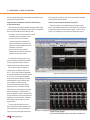
Figure 1: Using Templates
23
After the tool generates the code, you simply drag and drop the component into your environment file and Certe
Testbench Studio inserts the appropriate statements and then helps you fill out the instance name. If you change
a name, that value is propagated to the statements, as Figure 2 shows.
Figure 2: Adding the Generated Component
After you add the generated component into your environment, you typically need to write some of your own code,
such as filling out methods. Certe Testbench Studio lets you use Auto-Complete to correctly enter that code. At any
time, you can ask the tool to help you fill out a construct. Figure 3 shows the progression of Auto-Complete steps for
filling out the construction of a UVM component m_agent within a build method.
Figure 3: Using Auto-Complete
24
In addition, you can use Auto-Connect to assist in connecting the component. In an empty connect statement, you
can ask for the legal connections to use. Figure 4 shows that only the listed exports are legal for connecting the agent.
Figure 4: Using Auto-Connect
After you enter your code and save it, the tool will parse the file to find syntax and semantic errors,
saving you a simulator compile step.
Even though the tool generated the UVM component and helped you instantiate and connect it into your
environment, you did write your own code. To ensure that code is correct, use the built-in code checker (linter)
to find any violations. You can choose which rules that you want to run to match any coding standards that you
have established.
Capturing knowledge into templates and as code checker rules provides a powerful method to ensure
that your testbench code is correct, as Figure 5 shows.
Figure 5: Capturing Knowledge
25
Examine Several Perspectives
As you write your testbench, it often requires getting different perspectives on the code to ensure that mistakes
are not being made. Certe Testbench Studio provides you with several techniques to look at the same code from
several perspectives. You can visualize your UVM code structure to quickly see common errors such as unconnected
components or components that are not connected correctly, as Figure 6 shows.
Figure 6: UVM Testbench Structure
You can visualize any SystemVerilog or UVM class in standard UML (Universal Modeling Language) format
to detect common mistakes, such as inheriting from the wrong class or that you have a missing method in a class,
as Figure 7 shows.
Figure 7: UVM
Class Diagram
26
Finally, Certe Testbench Studio provides you with browsers that can be filtered to concentrate on particular data,
trace class hierarchy, or view available class methods. You can also create your own browsers.
Automate Register Generation
The register layer for the design and the testbench can contain thousands of registers. For example, 1000 registers
results in over 35,000 lines of code. Using Register Assistant, an option to Certe Testbench Studio, you can save many
hours of coding and opportunities to make mistakes, by letting Register Assistant generate the UVM register package
of your register layer and the associated documentation. If required, you can also generate the OVM register package
and the synthesizable RTL code using the same register descriptions as input, as Figure 8 shows. And, if there is any
change to the register descriptions, Register Assistant updates the register layer and documentation in seconds.
The automated register documentation is always up to date with the code and can be shared between all team
members. This documentation makes it easy to quickly spot missing registers or incorrect field definitions.
Figure 8: The Register Assistant Flow
Review the Code
Teams need to understand code relationships, navigate through references, and trace code through visualized
environments for design reviews. Instead of hand-drawing diagrams and poring over code printouts, you can use Certe
Testbench Studio to perform an interactive code review. This ensures that you are reviewing the actual code and saves
you significant time, by eliminating preparation time from the review process.
Conclusion
By using the automation and guidance features of Certe Testbench Studio, you can streamline
your testbench creation process and eliminate mistakes. These techniques should bring you much closer
to creating a flawless UVM testbench.
27
SystemVerilog Boot Camp
by Manu Lauria, DKOP Labs Pvt. Ltd.
This article will discuss how within a short time, students learned a
new set of Verilog constructs, and how to use them to solve specific
problems. We started with 30 students, fresh graduates from 25
different schools, chosen to undergo a “Verification Engineer” training
program as part of Mentor Graphics HEP (Higher Education Program)
initiative. The task – use an NCSU (North Carolina State University)
developed course to teach the chosen 30 students “SystemVerilog for
Verification”, enabling them to find good jobs in the industry.
This meant first teaching them the set of constructs that are
(loosely) part of the verification subset of SystemVerilog, and then use
all of those in verifying a given design. The design was a pipelined
16-bit microprocessor, the LC3, often used in universities for teaching
various courses. The functional parts of this design had been
protected, so the whole DUT was a black box for the students. The
design had been infused with tens of bugs, each of which could be
turned on and off by the instructors. Each student had a different set
of bugs, and the objective was to find all bugs using SystemVerilog
testbenches.
The course involved teaching them new data types (queues,
associative and dynamic arrays, structures, enumerated types
and strings), interfaces, procedures, object oriented programming,
randomizations, threads, interprocess communication and building
verification environments.
28
This was an intensive 30 days course, of 8 hour days. The lectures
took 52 hours, the labs and assignments another 48, and the two
projects were spread over 144 hours. The course spanned 6 weeks,
a much more compressed version than what is offered to students at
NCSU, who do the same over a 15 week period.
There were a total of 11 labs. The first 6 were small ones, designed
to reinforce the individual lectures. In Lab1, students wrote small
snippets to understand the new data types – enumerated types,
dynamic arrays, associative arrays, queues and strings – plus
operations and built-in functions for creating, reading, modifying and
deleting these new data types. In the second Lab, students worked
with tasks, functions, interfaces and clocking blocks. Lab3 was all
about OOPS – declaring classes, creating class objects, inheritance,
polymorphism, operations on class objects, properties and methods,
static-ness – all of this with an example from hardware design. In
Lab4, we delved into inter-process communication – semaphores,
mailboxes, and the new versions of fork/joins. Lab5 was all about
assertions, while Lab6 was a small exercise on functional coverage.
After these simple labs, we began the bigger ones, 5 of them. In
these, the objective was to put together more and more components
of the SystemVerilog language to verify actual designs. In the first of
these, the design-under-test was a small ALU and its pre-processor
in Verilog, and this had a few bugs inserted in the code. The first
lab had a test-bench that used classes, interfaces, some of the new
data types, programs, and stimuli, and put them together for the
purpose of exercising the DUT and discovering deviations from the
design specification. The second lab built on the first one, adding
object-oriented “send” structures, data payloads, randomization, tasks
and functions. In the third lab, another layer was added to the testbench – constraints were added to the random input variables, class
objects were extended to make them more specific - we approached
the typical structure for a comprehensive randomized self-testing
environment on the stimulus creation and driving side. Checking was
performed using probes into the internals of the DUT in a pipelined
manner. In the next lab, the checking of the response was also made
more structured and object-oriented, creating a comprehensive objectoriented, constrained-random, re-usable test and debug verification
environment. In the last lab, the aim was to get students acquainted
with some of the basic coverage features that Questa supports - the
creation of covergroups, coverpoints and cross coverage options - to
measure the completeness of checking DUT operations.
After these two sets of labs, we started with the projects. The first
of the project spanned 9 working days over 2 weeks. The DUT was a
simple non-pipelined 16 bit CPU with 16 instructions, separate units
for fetch, decode, execute, control and write-back, and two external
data and instruction memories. A much more complex example
than the one in the labs, the students had to spend quite some time
understanding the data sheet of the CPU before they could attack the
project itself. As mentioned, the task was to find bugs scattered all
over the Verilog code, which was protected from the students’ view
by using Verilog’s ‘protect directives. Students were required to use
all of what had been done in the labs – send and receive structures,
tasks, functions, constrained random stimulus generation, interfaces,
clocking blocks, mailboxes, concurrent and sequential assertions,
classes, inheritance, enumerated data types, associative/sparse
arrays. Each student was required to find 10-12 bugs.
This first project was somewhat easy, because bugs could be found
by applying each of the 16 instructions separately, even if with a variety
of data inputs (whether immediate data or from the memories). The
first few bugs could be found by focused and directed testbenches, but
some of the bugs were such that only a set of random inputs could find
them fast enough. The students were thus forced to use all the new
tools in their command – the whole gamut of SystemVerilog constructs
and methodologies covered in the course.
In the pipelined version of the CPU, each instruction was one
cycle after the other, and all the units – fetch, decode, control, writeback and execute – had to work in tight synchronization. Except that
in some cases, the pipeline was required to stall/wait, which made
the whole design much more complex. Moreover, the errors that
were introduced spanned multiple instructions, and only a particular
sequence of instructions would expose the introduced fault in the
Verilog code. This is where constrained randomization showed its
true powers, and where students could observe the power of the
constraints solver within Questa. They were also required to measure
coverage, so they used coverage assertions, metrics and score boards
to get a sense of how near they were to completion.
Some code snippets, indicating the kind of work done by the
students, are included at the end of this note.
The element of competition - “who finds all their bugs the fastest”
- turned the entire course into an intense game. It was observed that
the directed goal – finding bugs – made the learning of SystemVerilog
almost a corollary. Contrary to our observations in other courses,
where students retain only a small percentage of the course, this
course forced students to use almost all of what had been taught. For
many of them, the most difficult part was the object oriented aspects
and the assertions.
Within a span of 6 weeks, the students were ready to venture out
and verify the big bad designs the world would present to them, all
inside the powerful Questa verification environment.
Some of the students from this batch found jobs that actually use
SystemVerilog for IP verification. For many others, this was a useful
addition to their resume, making them more attractive for potential
employers.
Here are comments from the top 4 students of the class -
“The HEP program was very helpful. It brightened our
future, enabling us to enter the design/EDA industry.” Jitendra Aggarwal (now working at DKOP Labs, India)
“The HEP program was very well conceived and
executed. It gave us some useful experience, important for
our future career growth” - Amitav Banerjee (now working
at DKOP Labs, India)
29
“The program was very beneficial – gave us a sound
foundation, taught us the basics of the language & its
usage, & exposed us to real-life industrial challenges.”
- Vikas Tomar (topped the class, now working at Mentor
Graphics, India)
“The HEP program was not just a theoretical classroom training
program – there were logical and practical sessions based on a
“learning by doing” approach. The course material and real “scenariobased” lab exercises helped students understand verification
concepts easily” - Ruchi Bora (topped the class, now working at ST
Microelectronics, India)
Example 1 – The definition of a transaction class
class Transaction;
rand bit [15:0] Instr_dout;
constraint limit {Instr_dout [15:12] inside {1,5,9,14};}
constraint regvalue {
if(Instr_dout [15:12] == ‘LEA)
((Instr_dout[11:8] inside {[1:8]})&&(Instr_dout[8:0]
inside {[0:255]}));
else if((Instr_dout [15:12] == ‘ADD) && (Instr_dout [15:12]
== ‘AND) && (Instr_dout [15:12] == ‘NOT))
((Instr_dout[11:9] inside {[0:7]})&&(Instr_dout[8:6]
inside{[0:7]})&&
(Instr_dout[5] inside {0,1})&&(Instr_dout[4:2] inside
{[0:3]})&&(Instr_dout[2:0] inside {[0:7]}));
}
constraint last {
if((Instr_dout [15:12] == ‘ADD) && (Instr_dout [15:12]
== ‘AND) && (Instr_dout [15:12] == ‘NOT))
Instr_dout[11:9] != Instr_dout[2:0];
}
endclass
30
Example 2 – A Generator class definition
class Generator;
mailbox #(Transaction) gen2drv;
Transaction tr;
function new (mailbox #(Transaction) gen2drv);
this.gen2drv = gen2drv;
endfunction
task run;
tr = new();
assert(tr.randomize());
gen2drv.put(tr);
endtask
endclass
Example 3 – A Driver class definition
class Driver;
mailbox #(Transaction) gen2drv;
mailbox #(Transaction) drv2gol;
Transaction tr;
function new(mailbox #(Transaction) gen2drv, drv2gol);
this.gen2drv = gen2drv;
this.drv2gol = drv2gol;
endfunction
task drive_reset;
m1.reset = 1’b1;
#20;
m1.reset <= 1’b0;
endtask
task drive ;
gen2drv.get(tr);
this.tr = tr;
m1.complete_instr <= 1’b1;
m1.IR=tr.Instr_dout;
m1.IR1=tr.Instr_dout;
drv2gol.put(tr);
endtask
endclass
How Transactions Viewing Accelerates Debug
of Asynchronous SystemVerilog Designs
by Nicolas Leblond, Tiempo
This paper describes how Questa’s Verilog APIs for transaction
recording and viewing, allow the designer to create an effective debug
environment for asynchronous/clockless circuits utilizing Tiempo
technology.
It first introduces how to write high-level synthesizable models
of asynchronous circuits, and then shows how to use Questa’s
Verilog APIs to record transaction streams and attributes. It finally
illustrates how to debug clockless designs using those records.
As a result, the designer can see how the design, simulation and
debug of asynchronous circuits using Tiempo SystemVerilog coding
style, together with the Mentor Graphics Questa transaction-based
simulation environment is no more difficult than for conventional
synchronous circuits.
Transaction level models and coding
style for asynchronous circuits
Models are written in un-timed Transaction Level Modeling (TLM),
using the standard IEEE 1800 SystemVerilog language, while the
ACC netlist output is in standard gate-level Verilog format. Using
those formats provides a seamless integration of Tiempo clockless
technology into verification platforms like Questa, and lets the designer
access any required debug tools to find out the cause of possible
design mistakes.
Channels represent the basic medium for communication between
asynchronous design entities and processes. A channel allows
point-to-point communication between two processes, where each
communication through a channel involves a token exchange between
the two processes, via a “handshake”.
Handshake protocols can be of two kinds: push or pull. Each mode
defines which of the two processes involved in the token exchange is
the initiator of the handshake: the one writing data to the channel or
the one reading them.
Channels are modeled as SystemVerilog interfaces. Tiempo
developed SystemVerilog definition files and macros to predefine an
interface (i.e., channel type) for each of the SystemVerilog data types
(bit, byte, integer, etc…) as well as for user-defined types (e.g. typedef
or enumerated type).
Channel communications are modeled as read and write operations
using methods automatically created with each channel type. Those
operations can be blocking or non-blocking. Further information with
regards to Tiempo SystemVerilog coding style can be found in [2],
in which a simple FSM-ALU structure and its testbench are detailed.
Transaction support in Questa [3] is used to give a high level view
of the communication involved in the asynchronous design, through
those channels. The transaction view of the system is particularly
convenient as it hides the low-level implementation of those channels,
and gathers only the necessary information in a convenient format.
Using this higher level view, one can represent the channel state
(whether active or inactive), the start and end time of each channel
operation, and finally the relevant attributes characterizing it, such as
the occurrence of the operation or the token value at a given time.
Specifically, Questa transactions improve the simulation
and debugging of an asynchronous design by:
• detailing the sequences of token exchanges between
the different system modules in the design, whether
they are in the control-path or data-path
• providing the necessary fields for proper data monitoring
and verification
• giving a clear picture of the capacity and utilization
of the different channels in the system, when activated
To take advantage of this high-level view, a specific implementation
based on the usage of the appropriate Questa’s Verilog APIs is
necessary. The next section explains how this implementation
was done using Tiempo SystemVerilog definition files.
Using Questa’s Verilog APIs to record
channels transactions
Instrumentation of Tiempo SystemVerilog
definition files
The next two steps below detail how channel transactions are
recorded. They are illustrated with an example based on Tiempo
SystemVerilog code snippets of a bit-type, push-mode channel,
called “push_channel_bit”.
31
1st step, Creation of a channel stream
// bit-type and push-mode asynchronous channel declaration
interface push_channel_bit;
// Stream and Transaction Handle declaration
integer Stream_Op_Handle;
// One transaction handle is defined
// for each kind of channel operation: Read and Write
integer Transaction_Read_Handle, Transaction_Write_Handle;
integer ReadCount, WriteCount;
// Stream and counters initialization,
// ChOps stands for Channel Operations
initial begin
Stream_Op_Handle = $create_transaction_stream(“ChOps”);
ReadCount = 0; WriteCount = 0;
end
// push_channel_bit body, including Read and Write tasks
// see next figures for further details
task Read(output bit d)
//…
endtask
task Write(input bit d)
//…
endtask
We can note also, the declaration and initialization of two counters,
“ReadCount” and “WriteCount”, that will keep track of the occurrence
of Read and Write transactions.
2nd step, Read and Write transactions record
In Figure 2, and Figure 3, we show the transaction recording
process, associated with each kind of channel operation whether Read
or Write. Both of them relate to the “ChOps” stream, and operate in a
concurrent manner.
// non-blocking Read task
task Read(output bit d);
// Creating a READ transaction using the
‘push_channel_bit’ Stream
Transaction_Read_Handle = $begin_transaction
(Stream_Op_Handle, “READ”);
// Updating the transaction Id attribute with ‘ReadCount’
// to monitor the amount of Read transaction
ReadCount++;
$add_attribute(Transaction_Read_Handle,ReadCount,”Id”);
// body of asynchronous Read transaction
...
// end of body
// Once Read is done, closing and freeing transactions
// to avoid mem leakage
$end_transaction(Transaction_Read_Handle);
$free_transaction(Transaction_Read_Handle);
endtask
endinterface
Figure 2: Read transaction record
Figure 1: Defining the transaction stream for a channel interface
The first step of the transaction record is the creation of the
transaction stream for the given channel, using $create_transaction_
stream API as it appears in the “initial” block of Figure 1. This stream
is called “ChOps”. In this step, we store the handle returned by the
API into an integer variable, “Stream_Op_Handle”, which will be used
further for the creation of transaction sub-streams. Additional variables
are declared as well to designate Read and Write transaction handles.
They will be used when recording transaction attributes (as referred to
in the 2nd step).
32
// Write task
task Write(input bit d);
// Reusing the same Stream handle to create “WRITE” transaction
Transaction_Write_Handle =
$begin_transaction(Stream_Op_Handle, “WRITE”);
WriteCount++;
$add_attribute(Transaction_Write_Handle,WriteCount,”Id”);
// body of asynchronous Write transaction
...
// end of body
//adding “data“ attribute, ending and freeing
$add_attribute(Transaction_Write_Handle,d,”Data”);
$end_transaction(Transaction_Write_Handle);
$free_transaction(Transaction_Write_Handle);
endtask
Figure 3: Write transaction record
In each channel task, we simply start the related transaction with
a call to $begin_transaction, implement the body of the channel
operation, add the relevant attributes with $add_attribute, then end the
transaction and free it with $end_transaction and $free_transaction
calls. Attributes recorded in the Write transaction are “Id”, labeling the
transaction occurrence, and “Data”, carrying the value of the token. On
the other hand, the Read transaction attribute is only “Id”. This avoids
duplication of the Data field, which contains the same information as in
the Write transaction.
With such code instrumentation, each time a channel operation
such as Read or Write is triggered, a transaction is defined that logs
the different sequences of events within that channel. This information
can be further exploited in Questa, leveraging the different views of the
Graphical User Interface (GUI).
Those two simple steps show how easily one can create a
transaction level debug environment, for clockless SystemVerilog
designs.
Simulation flow setup to view
and debug channel transactions
With such an implementation, each channel instance has its own
record of transactions, and the different exchanges occurring into
the asynchronous circuit, when operating, are fully logged for further
analysis. But before moving further into the debug process itself, let’s
take a look at the simulation flow which can be applied to do so.
The design and debug flow of asynchronous systems can be divided
into the following steps:
• specify the system requirements, write the clockless design model
using Tiempo SystemVerilog coding guidelines, and set up
a testbench to verify against the specification
• run the simulation and record channel transactions
• post-process the results using Questa GUI and its transaction
level debug capabilities
Questa commands to run the simulation and record transactions
for further processing, are shown in Figure 4, following a two-step flow:
compile (vlog) then simulate (vsim).
We can also use the command line mode of the simulation, (i.e.
the “-c” switch), and perform analysis of the results in the GUI, with
the “-view” switch and with the data stored into the default “vsim.wlf”
dataset.
# work lib definition
vlib work
# compilation
vlog -sv -work work -mfcu -timescale “1ns/1ps” -64
+define+__STD_ASYNC_ENABLE_TRANSACTION
_RECORDING__
+define+CHANNEL_DELAY=#5
+incdir+${TIEMPO_INCDIR}
-v ${TIEMPO_LIB}/std_async_channels.sv
./testbench.sv ./dut.sv
# running simulation in command line mode
vsim top -c -do “run -all; quit -f”
# using GUI and generated dataset for post-processing debug
vsim -view vsim.wlf
Figure 4: Commands for a two-step flow and post-sim debug
It is worth noting the following switches for use during the vlog
compilation:
• -sv: makes the compiler compliant with SystemVerilog
•-mfcu: instructs the compiler to create one compilation unit from
multiple files. This is required due to the inclusion of Tiempo
SystemVerilog definition files
• +incdir+${TIEMPO_INCDIR} and -v ${TIEMPO_LIB}: these link
with Tiempo SystemVerilog definition files to define
and use any type of asynchronous channels
• +define+CHANNEL_DELAY=#5: sets the propagation delay
of channel transactions
• +define+__STD_ASYNC_ENABLE_TRANSACTION_
RECORDING__: triggers the transaction recording
of Tiempo channels
With regard to the simulation step, it’s not necessary to make
the transactions visible with the “-voptargs” switch or using the
“log” command. Indeed, as soon as the record tasks are called,
33
they are automatically logged into the dataset, provided the “nolog”
command has not been issued.
token flowing into a serial structure, with the red and blue rectangles
showing the first three sequences.
Asynchronous channels and their transactions
in the Questa GUI
Towards more instrumentation using TCL
Once transaction recording is enabled, the asynchronous design
can be debugged using the different views of the GUI. Transactions
data can be accessed across the following views:
Transaction objects are accessible through the full path of their
stream, sub-stream and attributes. One can develop TCL procedures
to improve the efficiency of the transaction debug. The TCL script in
Figure 7 is an example of a script which recursively seeks asynch-
• the “objects” view from which the user can select
the desired transaction object to monitor
• the “wave” view from which the user
can picture sequences of transactions,
figure out their data at a given time, and
perform a fine-grain analysis of the token
exchanges over the time
• the “list” view which gives a textual
representation of transaction events and
transitions over the time as well
The transactions viewing support in the
wave view offers the designer the possibility
to monitor graphically and over the time,
multiple transactions and their properties.
We can see in Figure 5 the display of
transactions of two different channel “OP”
and “Z”. The “ChOps” stream is expandable
to issue Read and Write sub-streams, labeled
as “C0” and “C1”, themselves expandable
to show their attributes. We can notice that
the Data attribute can be of different type:
in this example, the Data carried by
Z channel is based on a decimal radix (it
displays value -27), while Data carried by
OP channel is in enumerated type. From this
feature, the designer can easily perform a
fine-grain diagnostic, adding in the wave view
channel transactions that are suspected to be
implied in an incorrect operation, controlling
their attributes and that they occur in the
expected order.
Figure 5: how channel transactions look in the Wave view
The wave view also allows the user to
efficiently identify the different sequences of
token exchanges occurring in the design. In
Figure 6, we can picture eight sequences of
Figure 6: tokens flowing throughout the structure, in the Wave view
34
ronous channel instances in the design, and then adds to the wave
the associated “ChOps” stream. Such a procedure avoids the user
having to do this task manually.
handling the required type of data, using a simple macro (“DEF_
CHANNEL”), accessible with Tiempo SystemVerilog definition files.
// Inclusion of Tiempo SystemVerilog definition files
# tcl procedure to add to the wave view all channel transactions
// which enable the use of DEF_CHANNEL macro
# of an asynchronous design
`include “std_async_defs.sv”
proc {add_wave_chan_ops} {} {
set ch_inst_list [lsort [find instances -r -bydu *_channel_* -nodu]]
if {[llength $ch_inst_list] == 0} {
echo “no channel instances have been found”
} else {
foreach inst $ch_inst_list {
set st [find nets $inst/ChOps]
if {[llength $st] != 0} {
add wave $inst/ChOps
}}}}
// Types definitions
typedef bit [3:0] bit4_t;
typedef bit [5:0] bit6_t;
// Channels in push and pull modes defined thanks to a call
// to DEF_CHANNEL macro
`DEF_CHANNEL(bit4_t)
`DEF_CHANNEL(bit6_t)
// Example of channel instances in push mode,
// carrying the user-defined types of interest
push_channel_bit6_t A1 ();
push_channel_bit4_t Z1 (), Z2 (), Z3 ();
Figure 7: tcl script example to add transactions to the wave view
Figure 8: defining and instantiating channels
From these capabilities, the verification engineer can rapidly put in
place a set of procedures to augment the instrumentation of channel
transactions, and for example monitor the channel states, check the
token values, figure out root causes of a deadlock, and so forth. More
information on TCL scripting commands can be found in the Questa
reference manual [4].
handling user-defined type of data
Figure 8 gives the required steps to follow, when the designer needs
to create channels with user-defined types. The code also provides
an example of four channel instantiations A1, Z1, Z2 and Z3 being the
communication medium of the asynchronous unit further analyzed
below.
Application use-case
Asynchronous process of the unit
In this section, we describe issues that one can face when designing
a clockless circuit and how they can be debugged using transaction
views. A simple example is proposed to aid with understanding.
The computing unit in this example is a simple substitute box.
Figure 9 gives the SystemVerilog code of the “always” block modeling
its behavior.
A simple computing unit example
We first create asynchronous channels of user-defined type, and
then give the process details, used to access those channels and
perform the required computation.
User-defined type channels definition
User-defined types are preferred to model this example. The
following code shows how the designer can quickly create the channel
always begin : compute
// local variables storing input and output values
bit6_t a; bit4_t z;
// retrieving inputs
A1.Read(a);
// computing outputs with a macro
35
`SBOX_COMP
// sequentially sending results to three different channels
Z1.Write(z);
Z2.Write(z);
Z3.Write(z);
end
Figure 9: asynchronous process SystemVerilog code example
The unit produces a 4-bit value, given a 6-bit input and according
to a given constant table (refer to the text macro “SBOX_COMP”
provided in the annex). The computed result is sequentially issued
into three different channels.
The input data is retrieved from
A1 channel while the resulting
computation is produced on Z1,
Z2 and Z3 channels.
Assuming that EndRead() call was omitted, the related channel
would be blocked, which would lead to a deadlock situation. It would
have two consequences:
• a premature end of the simulation. Indeed as soon as the
EndRead() call is never issued, the process which performs
the corresponding Write operation on the same channel
will never get the hand back and would never proceed with
its remaining statements.
• additionally, no Data attribute would show up in the related
Write transaction. This situation is highlighted by the waveforms
in the top right corner of Figure 11, enabling to immediately
pinpoint channels implied in the deadlock. We can also use
“examine” command to display at the time of interest the content
of “ChOps” stream as shown in the bottom right corner.
Examples of asynchronous design debug
We briefly show in this part, two
different simple design mistakes
and how one can debug them
using the Wave view.
Deadlock issue
In this example, let’s assume the asynchronous process reading Z3
channel makes use of a blocking transaction to maximize the forward
latency of the unit. Blocking transaction can be modeled thanks to
the additional BeginRead() and EndRead() channel operations, which
respectively starts and ends the Read operation, holding the channel
access until EndRead() is issued. The code pattern in that case would
be the following:
Z3.BeginRead(data);
// process data
Z3.EndRead();
Figure 11: missing Data attribute when
blocking transaction never ends
Once the channel instance showing this symptom has been
identified, the designer can now go back to the SystemVerilog code,
look for the process that reads the channel if there is a missing
EndRead() call, and finally fix the issue.
It is also worth noting that this kind of mistake is flagged by Tiempo
ACC checker as a design error. The designer using this tool would see
the file, line number and channel name, which leads to the deadlock.
Incorrect computed data value
Figure 10: code pattern for blocking transaction
36
Another mistake which could occur would be an incorrect
computed value, in case for example, when a typo was introduced
in the substitution table. Say that, in correct operation, when the
input data is “110100”, the computed result should be “1001” (or 9 in
unsigned radix). Assuming that the actual value is 3, we would need
the necessary tool to track this issue, and understand its root cause.
Thanks to the display transaction Data field into the waveform, the
designer can more easily find out the mistake and investigate its
root cause. In Figure 12, we show the waveforms resulting from the
comparison of two runs, one which is incorrect, the other being the
gold reference. We can use Questa waveform compare tools, exactly
like it is done when debugging a synchronous system, to exhibit the
issue. The transcript window on the bottom-left of the figure and
in the waveform in the bottom-right corner show the result of this
comparison.
About Tiempo
Tiempo offers an innovative asynchronous and delay-insensitive
design technology [1], with a portfolio of powerful asynchronous IP
cores and a fully automated synthesis tool supporting these cores and
their design technology.
Chips designed in this technology and/or integrating these
asynchronous cores show outstanding physical properties such as
ultra-low power consumption, improved latency, and high robustness
to PVT variations.
Tiempo has developed a
comprehensive environment to
design asynchronous cores within
state-of-the art design flow. It
includes tools to:
• model asynchronous cores,
check their compliancy for
synthesis,
• perform their logic synthesis with
the Tiempo Asynchronous Circuit
Compiler (ACC) tool.
Annex
SystemVerilog macro
of the substitute box
Figure 12: comparing two waveforms
to figure out incorrect computation
Conclusion
Tiempo innovative technology nicely integrates into the Questa
verification and debug environment. The transaction support
significantly improves the productivity of the designer of clockless
systems, by offering the necessary views to efficiently diagnose design
failures.
References
Tiempo White-Papers: http://www.tiempo-ic.com/company/
technology.html
Technology Introduction
Introduction to SystemVerilog Asynchronous Modeling
Questa’s Documentation:
Questa SV/AFV User Manual
Questa SV/AFV Reference Manual
`define SBOX_COMP unique case (a)\
6’b000001,
6’b100010,
6’b001011,
6’b010000,
6’b000010,
6’b110001,
6’b101010,
6’b000101,
6’b011111,
6’b101011,
6’b010001,
6’b001100,
6’b100011,
6’b000100,
6’b000000,
6’b100001,
6’b111011,
6’b000110,
6’b100111,
6’b110101,
6’b100000,
6’b011000,
6’b010011,
6’b101111,
6’b100101,
6’b110100,
6’b010010,
6’b101110,
6’b110010,
6’b101000,
6’b100100,
6’b000011,
6’b011100,
6’b101101,
6’b001000,
6’b111000,
6’b000111,
6’b011011,
6’b010100,
6’b110110,
6’b100110,
6’b011001,
6’b111001,
6’b110011,
6’b010101,
6’b001101,
6’b001001,
6’b001010,
6’b111110:
6’b001111:
6’b101100:
6’b011101:
6’b101001:
6’b111100:
6’b111101:
6’b011110:
6’b001110:
6’b011010:
6’b111010:
6’b010111:
6’b010110:
6’b111111:
6’b110111:
6’b110000:
z=4’b0000;\
z=4’b0001;\
z=4’b0010;\
z=4’b0011;\
z=4’b0100;\
z=4’b0101;\
z=4’b0110;\
z=4’b0111;\
z=4’b1000;\
z=4’b1001;\
z=4’b1010;\
z=4’b1011;\
z=4’b1100;\
z=4’b1101;\
z=4’b1110;\
z=4’b1111;\
endcase
37
Lessons in Developing and Deploying OVM Compliant VIP
by Mike Bartley, Test and Verification Solutions and Andy Bond, Lead Verification Engineer, Icera
Using external VIP (Verification IP) brings several advantages
including availability, independence in both checkers and coverage,
robustness from use in several environments. However, the VIP
must be developed so that it is easy for the user to incorporate the
VIP into their environment. In this paper we look at practical lessons
learned in both the development and deployment of VIP for use in
complex OVM (Open Verification Methodology) SoC (System-on-Chip)
verification environments.
The VIP in question was deployed by Icera, a fabless semiconductor
company that develops chipsets for high-performance mobile broadband applications. Icera had a need for two new pieces of verification
IP. The first VIP they required was to be used in the verification of a
new SDCard interface they were adding to their chipset. They had
brought in the design IP from a supplier and wanted to source the
SDCard VIP from a different supplier for use in their chip level test
environment. The purpose of the verification environment was partly to
validate the design IP, but mostly to verify the integration of the IP into
the SoC and develop the lower levels of a SDC driver. The VIP was
able to mimic a number of SDCard standards (SDC, SDHC, SDXC)
and was also highly configurable thus enabling Icera to verify the
chip and their software in a wide range of configurations and settings.
The protocol checkers delivered with the VIP gave Icera confidence
that the design IP met the relevant specification. And the functional
coverage built into the VIP allowed Icera to ensure that they had
covered all the necessary scenarios in their verification.
Despite the lack of real-time constraints, simulation speeds
prevented Icera from actually running a full device driver. The level
of SW threading/context switching etc. is too complex, resulting in
excessive run times for even the simplest of tests. However, basic
routines such as card identification or individual SDC commands
upon which the driver is constructed may all be tested. In addition,
the nature of an SDC driver is advantageous for this style of top level
testing. The device driver must first identify available/connected SD
cards before establishing their capabilities. This allows the verification
engineer to construct a test program (or series of test programs) that
by their very nature should be agnostic to the SD card it detects.
As such the testbench was constructed to instance specific variants
of SD cards, similar to physically inserting different cards on an
evaluation board. These instances were configured using “ovm_test”
38
extensions, each with an individual set of factory overrides defining
the VIP’s capability. All other card characteristics, such as response
times, error responses etc. are left to be randomized using the
standard OVM sequencing seeded from the supplied SV seed. Using
this approach allows the same test program to be run varying only the
“ovm_test” configurations and random seed. Each simulation run is
equally valid, but each alters the execution flow through the SW and
HW. For example, under the SDC protocol, by default the card sends
the response “R1” for CMD11. However, the protocol allows for the
situation where the card does not respond. In order to program this
scenario into the SDCard VIP, the user sets the following command
in the test
set_config_int(“sve.tvs_sdc0.slaves[0].slave_engine”,
“hold_cmd11_resp”, user_val);
where user_val is either 0 (response enabled), and
1(response disabled)
This simple setting allows Icera to test that the design IP and
software correctly handles this corner case.
Icera already used OVM in their verification environment and so this
made it possible to get the VIP developed externally and then easily
integrated into their environment. The VIP was developed by TVS
(Test and Verification Solutions) who have many years of experience in
both developing and using VIP.
The VIP followed the OVM development guidelines but there were
also a number of lessons that were learned regarding the delivery and
integration of the VIP. For example, when delivering VIP the supplier
has to respect the fact that they don’t own the compile line. Each
switch the supplier requires on a command line is a switch that may
conflict with one that the customer is already using. Thus the supplier
should avoid any command line switches. In addition, the directory
structure / file-naming is important for several reasons.
• There must be an easy distinction between “deliverable” code
(code which makes up the VIP which will be used in other testbenches) and example usage code provided to prove the VIP.
In particular if the supplier does not take care the typedef’s,
constant declarations and define’s can find themselves in testbench code that won’t be part of a higher level test-bench,
but are required by the actual VIP.
• In order to easily integrate the VIP into a higher level build
structure, the “deliverable” directories must be easily isolated,
as the customer may only want to copy the VIP into their source
repository.
• Some simulators make distinctions between SystemVerilog and
Verilog code by file extensions, this can cause issues when built
into a higher level compile.
• Code that must be compiled should be easily identifiable from code
that must be included.
• Files that contain package declarations must be compiled before
code that uses that package. As such these files should be
identifiable by name.
Companies often also have their own mechanisms for such things
as messaging and objections and the supplier cannot assume that the
OVM mechanisms (“ovm_report”, “ovm_objection”, etc) are ubiquitous.
This is very common in companies with lots of C, C++, Specman,
etc. components in their test bench. A simple solution to this is to
use macros for each message / objection, defined in a separate file.
This allows the customer the ability to easily override these macro
definitions for simpler integration.
The second piece of VIP Icera that Icera required was OVM VIP
for several serial protocols (e.g. SPI, I2C, I2S). The Icera Livanto
digital baseband chip is a soft modem in
regards to digital processing. However,
by supporting a large number of off-chip
interface standards Icera can provide their
customers with more flexibility in their board
level design. For example, by providing
support for a large variety of serial protocols
for communication with PAs, PMICs, audio
chips etc. Icera customers can use the best,
most easily available and most cost efficient
components for their product. However,
this chip level flexibility is at the cost of the
verification effort required in proving each
individual protocol.
level packet, but the fundamental movement of data through a channel
is common. This opened up the prospect of creating a generic UVC
which can distinguish between the data-pump and the protocol so that
the majority of the testbench design can be re-used across standards.
The monitor/driver must be extended to understand the finer points as
do the protocol checkers and coverage, but the data score-boarding
can be completely re-used. By providing the test-bench integrator with
a common (pre-verified) score-boarding interface for connectivity/
integration testing not only is the total effort in test-bench development
reduced, but the verification engineers confidence in the VIP is also
increased.
Icera thus decided to take a novel approach to serial protocol
verification and asked TVS to develop a generic piece of OVM VIP
that could then be adapted to the various protocols. Figure 1 below
shows the typical structure of a block level test bench where the
generic serial IO VIP would be used. Of course, however, the generic
VIP would first need to be converted into a particular serial protocol
– I2C in this example. The object oriented features and factory
mechanism built into SystemVerilog and OVM enabled such an
approach as explained below. Below we discuss how to design
the VIP to allow for this specialization.
Figure 1: Generic Serial IO Slave VIP
Unfortunately there aren’t any shortcuts
with protocol verification. There can be an
element of re-use for related standards, but
fundamentally you have to treat each with
the same level of attention. That said, all
serial interfaces just basically move data
from one point to another, the packet format
may change or even be wrapped in a higher
39
The object oriented features allow us to create generic classes that
will be specialized for the various protocols. For example, generic
sequence items are generated to be used by the sequencer for
sending to the driver in the generic test bench. Figure 2 below shows
how these are then specialized for the SPI protocol
ovm_analysis_port #(tvs_sio_generic_slave_sequence_item)
slave_monitor_port;
Figure 3: Code demonstrating generic slave monitor
class tvs_sio_spi_slave_sequence_item extends
tvs_sio_generic_slave_sequence_item;
// Random Variable selecting which mode
of CPOL_CPHA Operation
rand spi_cpol_cpha_mode_e spi_cpol_cpha_mode;
// Random Variable selecting mode of data transmission:
MSB or LSB
rand spi_lsbfe_e
spi_lsbfe;
// Random Variable selecting mode of spi:
NORMAL or BI-DIRECTIONAL
rand spi_opr_e
spi_opr;
// etc
Figure 2: Code demonstrating specializing sequence item for SIO
Also, the slave monitor has an analysis port that allows it to connect
to the scoreboard. Figure 3 below shows how the analysis port sends
a generic sequence item to the scoreboard. This means that the user’s
scoreboard only has to deal with the generic sequence items rather
than sequence items for each protocol.
class tvs_sio_generic_slave_monitor extends ovm_monitor;
// Instantiatio of the Generic Virtual Interface
virtual tvs_sio_generic_intf generic_s_if;
// Instantiation of the Generic Slave Sequence Item
tvs_sio_generic_slave_sequence_item generic_xaction;
//PORT DECLARATION
40
Figure 4 below shows how the VIP user is able to connect
multiple slaves to the main test bench scoreboard.
class tvs_sio_top_scoreboard extends ovm_scoreboard;
// PORT DECLARATION
tlm_analysis_fifo #(apb_master_sequence_item)
prot_master_monitor_fifo;
ovm_analysis_export #(apb_master_sequence_item)
prot_master_monitor_export;
tlm_analysis_fifo #(tvs_sio_generic_slave_sequence_item)
spi_slave_monitor_fifo;
ovm_analysis_export #(tvs_sio_generic_slave_sequence_item)
spi_slave_monitor_export;
tlm_analysis_fifo #(tvs_sio_generic_slave_sequence_item)
i2c_slave_monitor_fifo;
ovm_analysis_export #(tvs_sio_generic_slave_sequence_item)
i2c_slave_monitor_export;
function void connect;
prot_master_monitor_export.connect(prot_master_monitor_
fifo.analysis_export);
spi_slave_monitor_export.connect(spi_slave_monitor_
fifo.analysis_export);
i2c_slave_monitor_export.connect(i2c_slave_monitor_
fifo.analysis_export);
endfunction: connect
Figure 4: Code demonstrating connecting multiple slaves to a
scoreboard
The DUT and the VIP are connected using a System Verilog
interface. The generic interface is adapted to specific protocols using
the “modport” mechanism. Now that TVS has completed the generic
slave code, the only changes required to the generic code to add an
additional protocol is to add the required signals and define a modport
specific for the protocol. The generic code then has to be extended for
the particular protocol.
3. Instantiate the tvs_sio_env in the top level environment.
4. Create the object of the tvs_sio_env in the top level environment
and pass the number of generic agents you want to create as
shown below.
interface tvs_sio_generic_intf(input logic clock);
// variables for the various interface signals
// Instance of the SPI Slave Driver Modport
modport spi_sd_mp (input spi_sck, spi_ss, spi_mosi_en,
output spi_miso_en);
5. Create the necessary connections for the tvs_sio_env:
// Instance of the SPI Slave Monitor Modport
modport spi_sm_mp (input spi_sck, spi_ss, spi_mosi_en,
spi_miso_en);
// Instance of the I2C Slave Driver Modport
modport i2c_sd_mp(input clock, scl_s_in, sda_s_in, output scl_s_out, sda_s_out);
// Instance of the I2C Slave Monitor Modport
modport i2c_sm_mp(input clock, scl_s_in, sda_s_in,
scl_s_out, sda_s_out);
endinterface: tvs_sio_generic_intf
Figure 5: Code for using the interface
The user of the VIP has a few very simple steps to go through.
1. Instantiate the tvs_sio_generic_intf instance in the test bench top.
2. Use the ovm function set_config_object to replace the generic
interface present globally with top level instance as show below.
a. Connect the user top level virtual sequencer with the generic
sequencer used inside the tvs_sio_env.
b. Connect the generic monitor output ports to the user
scoreboard.
6. The user can make the necessary configurations in their virtual
sequence.
7. The necessary configurations to be done by the user at the test
case are as shown below.
a. Setting the number of generic slave to be used.
b. Setting the generic slave agent to be in the active mode.
c. Setting the generic agent sequencer count to be zero, as the
sequence operations are going to be controlled from the virtual
sequencer.
41
d. Use the set type override instance by type function to factory
override the generic slave components using the protocol
specific components.
e. Variable setting necessary for the protocol agent monitor.
This paper has considered the issues beyond those covered in the
OVM manual to ease integrating OVM VIP into an OVM test bench.
It has demonstrated how a well constructed VIP can allow the user
to easily adjust the configuration settings to test both their hardware
and software in various corner cases. It has also demonstrated
how the object oriented features and factory mechanism built into
SystemVerilog and OVM has allowed TVS to build a generic serial
interface VIP that is easily adapted for different protocols.
42
A Full Function Verilog PLL Logic Model
by Mohammad Ashraf, VeriCon
This paper describes the full function model of a phase locked loop
(PLL) in a logic simulator. In contrast to conventional models that
bypass the PLL function, this Verilog model accurately represents all
major characteristics of a PLL.
nothing more than a bypass mux. This method is useful to the extent
that the designer can implement his/her logic without having to worry
about the special issues surrounding a PLL, such as lock-up, jitter and
other phenomena.
It allows the simulation of the effect of the actual filter elements.
It can accurately model clock deskew of a clock tree as well as
synthesize other frequencies from the input clock. It produces a lock
detect signal after a realistic lock sequence. The user has the option
to add jitter to the PLL output. The model performs three orders of
magnitude faster than an equivalent circuit model.
However, such workarounds do not adequately represent the real
time behavior of the actual PLL and in some cases do not allow the
simulation of a larger system at all. The latter is particularly true where
the PLL is used for frequency synthesis with dynamic frequency
switching.
Introduction
On-chip phase-locked loops (PLLs) have become common place
in Application Specific Integrated Circuits (ASICs). Initially esoteric
circuitry required custom design techniques, they are today standard
offerings in gate array and standard cell libraries of most ASIC
vendors. Their main functions in digital circuitry are clock-deskew,
frequency synthesis and clock recovery from data signals.
Even though PLLs are well established they are still advancing
rapidly in various performance parameters such as frequency range,
jitter and lock time. Other advances are adding filters sensitivity or
reduction of power supply.
However, there is one lingering shortcoming of PLLs that is
associated with their logic model. Because of the intricate inner
workings of a PLL, an accurate representation of its function has
commonly only been achieved with circuit type simulators such as
SPICE. Circuit models are necessary for the design of the PLL itself
but unfortunately, for chi level simulations a circuit type model is not
useful because a) the model typically is not compatible
with a logic simulator, and b) even if a mixed mode
(analog/digital) simulator is used, the simulation times
for the PLL are exorbitant amounting sometimes to
days to achieve lock.
This article describes a Verilog logic model of the PLL that allows
the Verilog simulation of all relevant PLL phenomena such as real
clock deskew, frequency synthesis, lock-up behavior including lockdetection, effects of the filter parameters on the PLL behavior and
even jitter.
Model Structure
Figure 1 shows the building blocks of a Verilog PLL model. The
phase detector takes two clock inputs and generates the up/down
pulses.
The width of the up/down pulses is directly proportional to the
phase differences of the clock input. The up/down pulses are then
applied to the input of an up/down counter which increment/decrement
the count proportional to the width of up/down pulses. The numeric
controlled oscillator generates an output clock signal whose frequency
is proportional to the input count.
Fig 1. Building blocks of Verilog PLL model
Most digital designers “bypass” the problem in
the true sense of the word. Rather than attempting
to simulate PLL behavior in the context of a digital
chip or system, they bypass the PLL by means of a
multiplexer. In fact mostlogic models of PLLs are
43
Frequency Phase Detector (FPD)
It compares the phase of the reference (input) clock “ref”, with the
phase of the feedback clock generated “fb” from the NCO. It creates
an up pulse when “fb” clock input has phase lags “ref” input. Similarly it
creates a down pulse when “fb” clock input has phase leads “ref” input.
Pseudo Verilog code for Frequency Phase Detector.
always @(posedge ref)
if (fb == 1’b0)
begin
ref_up_time = $realtime;
if (ref_up_time > fb_up_time)
up = 1’b1;
if (down == 1’b1) down = 1’b0;
end
//
always @(posedge fb)
if (ref == 1’b0)
begin
fb_up_time = $realtime;
if (fb_up_time > ref_up_time) down = 1’b1;
if (up == 1’b1) up = 1’b0;
end
always @(negedge up)
if (up_time != 0.0)
begin
width = $realtime - up_time;
count = count + width ;
end
//*********************************
// Measure the width of down pulse
//*********************************
always @(posedge down) down_time = $realtime;
// Measure pulse width in ns, ignoring first pulse at 0
// simulation time
always @(posedge down)
if (down_time != 0.0)
begin
width = $realtime - down_time;
count = count - width ;
end
Numeric Controlled Oscillator (NCO)
//
always @(negedge ref) ref_up_time = 0.0;
//
always @(negedge fb) fb_up_time = 0.0;
Up/Down Counter
Start with an initial count, it measures the width of up/down pulses
generated by Phase detector and increments/decrements the count
accordingly.
Pseudo Verilog code for Up/Down Counter.
//********************************
// Measure the width of up pulse
//********************************
always @(posedge up) up_time = $realtime;
// Measure pulse width in ns, ignoring first pulse at 0
// simulation time
44
It generates the clock whose frequency is proportional to the input
count value.
Pseudo Verilog code for Numeric Controlled Oscillator.
initial
begin
ck = 1’b0;
forever #(next_phase)
ck = !ck;
end
//
always @count next_phase = Constant/count ;
SIMULATION SNAPSHOT
Performance
The following Modelsim results show the typical signal waveforms
for a clock deskew behavior of the model.
Compared to circuit simulators the performance of our PLL
simulation in Verilog was improved by almost 3 orders of magnitude.
While an HSPICE simulation would require approximately 48 hours
to achieve lock, the Verilog model would complete the same task
in 4 minutes.
The figure 2 is the Modelsim waveform snapshot at the beginning
of the simulation. The first signal is the input reference clock. The
second signal depicts the feedback clock that attempts to lock onto
the reference clock. It is apparent that both clocks are far apart
in their respective frequencies.
Figure 2
The figure 3 is the Modelsim waveform snapshot at the end
of the simulation when feedback clk has achieved perfect lock with
the reference clock and the lock detect signal is asserted.
Conclusion
The presented Verilog model
of an analog PLL accurately
reflects all relevant physical
features of a PLL. In particular it
allows realistic simulation of clock
deskew and frequency synthesis.
It also represents accurately the
lock sequence including the lock
detect signal, based on the choice
of filter elements. Finally, at the user’s discretion, an arbitrary amount
of random jitter can be added to the PLL output signal. The model
performs almost three orders of magnitude faster than an equivalent
circuit model.
Figure 3
Other Features
We have added other features to our Verilog PLL model. The filter
components, R and C, can be entered by the user into the model, thus
emulating the actual lock behavior of the circuit including damping
phenomena due to the particular filter characteristics.
One other feature is the optional addition of jitter to the PLL output
by making use of a random function generator in Verilog, the user
can add any desired jitter amplitude to the NCO period, thus allowing
realistic worst case system simulations.
45
Document Driven Verification (DDV):
Ready to Throw Out Your Verification Plan?
by Peet James, Mentor Graphics Consulting
Introduction
Not having a good list of specifications for a large SOC design
kills the project before it starts. The verification team, as the first
customer of such a design, relies on the specs to build a set of realistic
scenarios around the design. These scenarios comprise a verification
world that is almost always bigger and more complicated then the
design being verified. Accordingly, building this world often requires
more effort and time than building the design itself.
Verification is not a linear or deterministic process. Theoretically we
could verify forever and still not verify everything. Since schedules are
always constrained and deadlines are a fact of life, decisions must be
made to determine how to get the best and most verification done in
the allotted time. To do this, successful verification teams think through
and document their verification plan upfront, a difficult but ultimately
worthwhile process.
Building a “verification plan” is fraught with challenges, including
disagreement about what the phrase means. To some it is a short list
46
of features or testcases to try. To others it is a 1,000-page reference
document.
Instead of fretting over definitions, it’s more productive to begin
thinking in terms of how verification will be documented quickly and
in such a way to drive the overall verification effort. We call this
document driven verification, or DDV, and the idea can be summarized
in three short exhortations:
• plan early
• plan together
• then capture the plan in a family of easy to make
and maintain documents.
This article focuses on the second and third points. The first point,
on why and how to plan early, is addressed in a verification planning
and management series of videos on Mentor Graphics Verification
Academy (http://verification-academy.mentor.com).
The nature of documentation
Let’s be realistic. Documentation is not the most exciting part
of engineering. It is a necessary evil, full of potential pitfalls and
challenges. Among these:
1. The creation dilemma: In some companies, one person is more or
less sequestered for several months writing all the documentation.
When at last the document is done, everyone involved (except the
author) typically will peruse the tome once, then use it only as a
reference manual, due to lack of collective ownership.
2. The format dilemma: A verification plan ranges from high-level
information presented in a narrative flow with illustrations to lowerlevel details that demand lists or spreadsheets. Piecing all this
content together is seldom done well.
3. The language dilemma: The English language is inherently
ambiguous and imprecise, a situation compounded by the jargon
in EDA and semiconductor design. Accordingly, the list of easy-tointroduce errors is long: errors of omission, errors of commission,
errors of clarity, errors of understanding and so on. Check any
technical publication for terms like “system”, “component” and
“error”. How often are there multiple ways to interpret each?
4. The engineer dilemma: Engineers aren’t known for their writing
skills. We use a lot of technical jargon and occasionally make up
our own words. When we get tired of writing out the words, we
turn them into acronyms, or even acronyms embedded in other
acronyms. Remember VHDL – VHSIC hardware description
language? Engineers also tend to skip the step of describing a
problem and instead dive right into implementation. Finally, like
most people, engineers believe that spending time writing planning
documents will cause delays. Actually the opposite is true. The
Crawford Greenewalt adage – “every moment in planning saves
three or four in execution” – is often accurate.
5. The length dilemma: Any technical document that exceeds 40
pages in length is hard to write, read and maintain. This doesn’t
stop most organizations from producing such documents,
which ostensibly offer the benefit of putting all their verification
information in one location. It is far superior, for readers and
editors to deal with several shorter documents.
6. The company dilemma: Most organizations do not emphasize
technical writing, which is why engineers so often wind up doing
the documentation in the first place. It’s almost always more
productive to have a good engineer do engineering work and
to maintain at least a small staff of writers to support their more
technical counterparts. Another key role, rarely emphasized, is
that of the facilitator, whose job it is to keep things focused and
gracefully handle the inevitable conflicts.
7. The maintenance dilemma: Even if you create good documents,
they have to be kept up-to-date in order to remain useful. Unless
maintenance is part of the established process, the pressures of
other “more important” tasks will crowd in.
With all of these working against us, how do we create
documentation as efficiently as possible? Most important by far
is sharing the burden of creation. Many perspectives – those of
architects, designers, tools people, IT engineers, technical writers,
etc.) – are better than one. The issues that come up while soliciting
different viewpoints are usually those that turn into problems later. And
the process of creating the document, which invariably fosters a sense
of shared ownership, is actually more important than the contents of
the document.
Each document in a plan needs to have a purpose that is clear to
its intended audience, which can range from verification managers to
debuggers. Taken together, the documents should address building
(what we will build and in what order), running (run management,
results analysis, bug finding and tracking) and functional coverage
(modeling, analysis and closure).
A family of verification documents
It’s possible to borrow techniques used by engineers working on
SOC designs. Some of these engineers eschew documentation
completely, which is problematic if the key person on the project gets
hit by a bus. Some go a little farther and make quick informal lists
of features to implement. This approach can be sufficient for small
designs but inadequate as complexity grows. On the other end of the
spectrum, engineers working on very large SOC designs typically
end up using a family of documents to describe their design. Figure 1,
below, shows an example of a common document structure.
47
The document family typically starts out with a single design
architecture document (DAD) that gives a system level picture of the
design. The primary purpose is to show the entire SOC and how
each subsystem is interconnected. Often the size and/or complexity
of the design results in a DAD that is unwieldy. If this is the case, it
is split into sub-system DADs, each with its own micro-architecture
information showing how the subsystem blocks are interconnected.
When these get too big and more detail is necessary, design
implementation documents (DIDs) are usually needed. These detail
the actual state machines, timing diagrams, registers and so on.
covered. The verification requirements spreadsheet is often called a
trace matrix. Other traceable information, (priorities, status, author,
owner and so on) can be added for each requirement and the data
used to produce a metric dashboard.
Figure 3 shows how these big-picture and granular-detail documents come together to create a family of verification documents.
The main challenge: properly characterizing each piece of information (high- or low-level) and then placing it in the correct level
of the hierarchy.
Figure 2 shows how verification teams can borrow the family of
design document architecture and implementation approach, modify it,
and reuse it for their own purposes.
Figure 3: A Family of Verification Documents
Figure 2: Hierarchy of verification documents
Successful verification teams create and use a hierarchical family
of documents, starting with a single parent document. This verification
architecture document (VAD) is used to describe the overall strategies
and architectures of the verification project. When it gets too long (in
excess of 40 pages), we start breaking off verification implementation
documents (VIDs). Typical VIDs address generation, scoreboard
checking, assertion checking and/or functional coverage. Other
verification piloting documents, such as user information, coding rules
(conventions, templates, etc.), wikis and how-to information start off in
the VAD and are eventually broken off into separate child documents.
The lowest-level details – these include scoreboarding elements,
assertion and coverage items, and so on – are captured outside the
VIDs, usually in a spreadsheet. Each verification requirement on the
spreadsheet can be linked to a functional coverage group or item, an
assertion, a directed test or other links. Questa’s Verification Manager
with its universal coverage database (UCDB) can then track and trace
each requirement, gathering and analyzing until each has been fully
48
What’s in a VAD?
To keep it accessible, the top-level VAD should not exceed a
maximum length of 40 pages. Where information is pulled from the
VAD, a paragraph is inserted summarizing the new child document
and referencing its location. And when a document is pulled out of the
VAD, it is a good time to assign the new child document to another
person on the verification team. This spreads the maintenance efforts,
and allows a broader ownership of the information. Most projects
use an internal, secure project website and keep the parent and child
documents together.
A VAD typically starts out with an introduction section that includes
a mission, goals and scope. Next comes a strategy section that might
address several of the following categories.
1. General approach: “Full self checking is a goal of this verification
effort, but a reference model is not available, so an overall endto-end scoreboard cannot be built. Instead, the plan is to build
simple scoreboards over the abc input data path, as well as the
xyz outbound path, along with several sets of strategically placed
assertions in the def, ghi, and jkl blocks.”
2. Reuse: “Build a block-level testbench that is coded in such a way
to be easily reusable at both the subsystem and system level.”
3. Libraries: This might be a description of which parts of OVM you
will use or avoid, and how they will be used. Another example
might be a migration strategy from OVM to UVM.
4. Change management: “Last project we used SVN for the first
time and it was worthwhile, but we did not have a universal set of
check-in rules or consequences for everyone to follow. This cost
us many wasted regression runs. So …”
5. IP qualification: “We have had quality IP in the past and we have
had garbage. An IP qualification process will be created to weed
out the garbage.”
for the trace matrix. These preliminary implementation descriptions
are eventually broken off as VIDs once they have grown to a
substantial size.
What’s in a VID?
Because of similarities to C++, VIDs are typically modeled after
software implantation documents. The aim of such documents is to
show data-fields and methods of all major code interfaces. Unified
modeling language (UML) diagrams are used as a format to show
code extending, encapsulation, polymorphism and interfacing.
Sequence UML diagrams are also useful here.
Next is the VAD’s architecture
section, which usually includes:
1. Block diagrams: One or
more testbench-level diagrams
that show the overall verification
components and their
interconnections.
2. Component tables: A corresponding (to the block diagram) list of
testbench files (test, top, env, etc.),
components (agent, sequencer,
driver, monitor), transactions, scoreboards, and coverage files,
each with lines of code (LOC) estimates. These estimates can be
reworked into a schedule if needed.
3. Layers: Typically a column is added to the component table citing
the defined layering approach. If object oriented programming
(OOP) code, such as SV, is not encapsulated and layered
(extended) properly, it quickly turns into spaghetti.
4. Phases: Most testbenches require a lot of code writing. In order
to get results quickly, we want to build the testbench in a logical
set of sequences, each of which builds on the previous one. This
section of the VAD lists each milestone. Phases are added to the
component table, as well.
Next is the implementation section of the VAD, which includes
use models for generation/sequencers and scoreboarding architecture.
General locations of assertion and coverage groups are provided,
including how they will be named and controlled. The specific list of
assertions and coverage detailed verification requirements are left
What’s in a Trace Matrix?
Figure 4 above shows an advanced trace matrix example.
The light blue columns at left hold the design requirements (DRs).
The green columns are the verification requirements (VRs) that
correspond to (and have been translated from) that row’s DR. The VRs
are divided into generation, checking (scoreboard and/or assertions)
and straight functional coverage. The red columns link to Questa’s
Verification manager and have a name (of the actual assertion,
coverage group, coverage item, or test name) and a link (there is a list
of about 10 types in the Questa documentation). The purple columns
are extra traceable information, such as priority or author, added for
each requirement to facilitate gathering requirement metrics.
Simpler trace matrices are limited to gathering and placing
verification requirements, one per row, into the spreadsheet. Such
metrices are typically divided into sections for generation/sequences,
checking (scoreboarding and assertions) and straight functional
coverage groups. Capturing all requirements in one spreadsheet
49
can be difficult given design complexity. If more than one spreadsheet
is used for any reason, each can be linked by strategic labeling and/or
numbering. (For more information on linking requirement spreadsheets
to Questa, see the Questa verification manager documentation.
Reqtracer also is a useful tool to store and keep track of requirements.)
Summary
This article outlines the family of documents that can comprise
a useful verification plan. We did not focus on how to create the
documents themselves, which is something best learned by working
together in a group. Mentor Consulting has a verification planning and
management consulting module that shows a team how to implement
DDV on their project. It includes best practices and tactics applied
directly on the actual design, including making a real VAD and/or test
matrix. But for now, here’s the bottom line on process: Start with a
VAD and then break out any sections that grow too lengthy into VIDs
or other child documents. Keep each document relatively short and
focused. Regularly review and maintain all documents . And always
ask if your documentation will actually drive the building, running and
closing of a maximum verification effort in a minimum amount time.
50
51
Editor: Tom Fitzpatrick
Program Manager: Rebecca Granquist
Wilsonville Worldwide Headquarters
8005 SW Boeckman Rd.
Wilsonville, OR 97070-7777
Phone: 503-685-7000
To subscribe visit:
www.mentor.com/horizons
To view our blog visit:
VERIFICATIONHORIZONSBLOG.COM
52