1
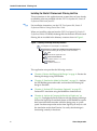
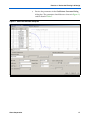
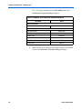
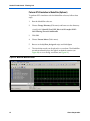
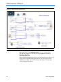
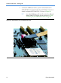
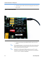
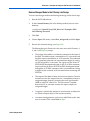
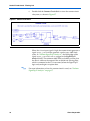
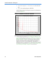
Stratix II Professional
Filtering Lab
Application Note 393
August 2005, version 1.0
Introduction
The Stratix ® II filtering lab design in the DSP Development Kit, Stratix II
Professional Edition, shows you how to use the Altera® DSP Builder for
system design, simulation, and board-level verification. The DSP Builder
digital signal processing (DSP) development tool interfaces
The MathWorks industry’s leading model-based design tool, Simulink,
with the Altera Quartus® II development software. DSP Builder provides
a seamless design flow in which you can perform algorithmic design and
system integration in The MathWorks MATLAB and Simulink software
and then port the design to hardware description language (HDL) files
for use in the Quartus II software.
Using DSP Builder, you can automatically generate a register transfer
level (RTL) design and a testbench from Simulink. These files are
pre-verified RTL output files that are optimized for use in the Altera
Quartus II software for rapid prototyping. The built-in DSP Builder
SignalTap® II Analysis block allows you to capture signal activity from
internal device nodes, while the system under test runs at system speed
in hardware. You can import the SignalTap II data into the MATLAB
Workspace browser for further analysis.
The Stratix II Professional filtering lab uses the following items:
■
■
■
■
■
■
■
■
Altera Corporation
AN-393
Quartus II software
DSP Builder with the SignalTap II logic analyzer read-back feature
Altera FIR Compiler MegaCore® function
Altera NCO Compiler MegaCore function
The MathWorks MATLAB and Simulink system design and
modeling tools
Stratix II EP2S180 DSP development board
Stratix II Professional II filtering lab design
(Optional) Mentor Graphics® ModelSim®-Altera, ModelSim PE, or
ModelSim SE simulation software
1
Stratix II Professional Filtering Lab
Installing the Stratix II Professional Filtering Lab Files
These instructions in this application note assume that you have already
installed the software provided with the DSP Development Kit, Stratix II
Professional Edition on your PC.
f
For installation instructions, see the DSP Development Kit, Stratix II
Professional Edition Getting Started User Guide.
When you install the software from the DSP Development Kit, Stratix II
Professional Edition CD-ROM, the design files for the Stratix II Professional
filtering lab are installed in the directory structure shown in Figure 1.
Figure 1. Filtering Lab Design Directory Structure
<install-path> The default path is C:\altera\kits\
StratixII_Pro_DSP_Kit-v1.0.0\Examples\HW\Lab\Filtering
Contains the filtering lab design files and documentation
Doc
Contains this application note
Exercises1and2and3
Contains exercise 1, 2, and 3
Exercise4
Contains exercise 4
This application note provides the following exercises:
2
■
“Exercise 1: Review the Filtering Lab Design” on page 4—Review the
filtering lab design using DSP Builder.
■
“Exercise 2: Simulate the Model in Simulink” on page 21—Analyze
the DSP Builder-generated models and simulate the filtering lab
design in Simulink.
■
“Exercise 3: Perform RTL Simulation (Optional)” on page 25—
Perform RTL simulation using the ModelSim simulation tool.
■
“Exercise 4: Analyze & Compare the Results in Hardware” on
page 29—Configure the Stratix II device with the filtering lab design
and use the SignalTap II read-back feature in DSP Builder to capture
data from internal device nodes while the design runs at system
speed. You then compare the results from SignalTap II analysis with
the simulation results from Exercise 2 to verify that the design is
functioning correctly in hardware.
Altera Corporation
Stratix II Professional Filtering Lab
Before You
Begin
You must have the following software installed on your PC:
■
■
■
■
■
■
1
Quartus II software version 5.0 Service Pack 1
DSP Builder version 5.0.1
FIR Compiler MegaCore function version 3.2.1
NCO Compiler MegaCore function version 2.2.2
The MathWorks Release 14 with Service Pack 2 (R14SP2):
●
MATLAB version 7.0.4
●
Simulink version 6.2
(Optional) ModelSim-Altera, ModelSim PE, or ModelSim SE version
6.0c
ModelSim-Altera is not included with the Quartus II Software
Development Kit Edition (DKE) version 5.0 that is bundled with
the DSP Development Kit, Stratix II Professional Edition.
This application note assumes that you have installed the
software into the default locations.
You must run the DSP Builder setup script once, following the
installation of MegaCore functions. The script updates DSP Builder for
newly installed or upgraded cores.
f
For more information see the Using MegaCore Functions chapter in the
DSP Builder User Guide.
To run the setup script, follow these steps:
1.
Run the MATLAB software.
2.
In the Current Directory list in the desktop toolbar (see Figure 2),
browse to the directory:
<dsp-builder-install-dir>\DSPBuilder\AltLib
3.
Type the following script in the MATLAB Command Window (see
Figure 2):
setup_dspbuilder r
3
Altera Corporation
Stratix II Professional Filtering Lab
Figure 2. Setting the MATLAB Current Directory to DSPBuilder\AltLib and Running the Setup Script
4.
Exercise 1:
Review the
Filtering Lab
Design
When you see “DSP Builder v5.0.1 setup completed,” as shown in
Figure 2, this procedure is complete. You can now use the exercises
in the filtering lab design.
To review the filtering lab design, follow these steps:
1.
Run the MATLAB software.
2.
In the Current Directory list in the desktop toolbar (see Figure 3),
browse to the directory:
<install-path>\StratixII_Pro_DSP_Kit-v1.0.0\Examples\HW\
Lab\Filtering\Exercises1and2and3
1
MATLAB file operations use the current directory and the
MATLAB search path as reference points. Any file you want
to run must either be in the current directory or on the
search path. The search path is set with the Set Path
command (Tools menu).
Figure 3. Setting the MATLAB Current Directory to Exercises1and2and3
3.
4
Choose Open (File menu), select filter_design.mdl, and click Open.
Altera Corporation
Stratix II Professional Filtering Lab
4.
Review the Simulink design (see Figure 4).
The filtering lab design contains a combination of
OpenCore® Plus DSP MegaCore functions and DSP Builder blocks.
The OpenCore Plus feature lets you test-drive Altera
MegaCore functions for free. You can verify the functionality of a
MegaCore function quickly and easily, as well as evaluate its size and
speed before purchasing the software. The OpenCore Plus feature
also provides a free hardware evaluation feature, which allows you
to generate time-limited programming files for designs that include
Altera MegaCore functions. You can perform board-level design
verification before deciding to purchase licenses for each used
MegaCore function. You only need to purchase a license when you
are completely satisfied with a core’s functionality and performance,
and will take your design to production.
f
5
For more information on the OpenCore Plus hardware evaluation, see
AN320: OpenCore Plus Evaluation of Megafunctions.
Altera Corporation
Stratix II Professional Filtering Lab
Figure 4 shows the top-level schematic for the filtering lab design. Two
numerically controlled oscillators (NCOs) generate a 1-MHz sinusoidal
signal and a 10-MHz sinusoidal signal respectively. The signals are added
together and then passed to a low-pass filter with a cut-off frequency of 3
MHz. The low-pass filter removes the 10-MHz sinusoidal signal and
allows the 1-MHz sinusoidal signal through to the fir_result output.
Figure 4. Simulink Design for Exercises 1, 2 & 3
6
Altera Corporation
Stratix II Professional Filtering Lab
Review the NCO_1MHz MegaCore Function Instance
To review the parameters for the NCO_1MHz MegaCore function, follow
these steps:
1.
Double-click the NCO_1MHz block (see Figure 4) to launch IP
Toolbench for the NCO Compiler MegaCore function, as shown in
Figure 5.
Figure 5. IP Toolbench for NCO Compiler MegaCore Function v2.2.2
2.
7
Click Step 1: Parameterize to review the parameters for the
NCO_1MHz block (see Figure 6 and Figure 7 on page 10). The
NCO_1MHz block generates a 1-MHz sinusoidal signal and is
implemented using the multiplier-based architecture, which
reduces memory usage by using the hardware multipliers in the
Stratix II device.
Altera Corporation
Stratix II Professional Filtering Lab
a.
Review the parameters in the Parameters tab. The parameters
should be set as shown in Figure 6, and are listed in Table 1.
Figure 6. 1-MHz Sinusoidal Signal - Parameters Tab
8
Altera Corporation
Stratix II Professional Filtering Lab
Table 1 lists the parameters for the NCO_1MHZ block that you
can set in the Parameters tab.
Table 1. NCO_1MHz Compiler - Parameters Tab
Parameter
Value
Under Generation Algorithm
Multiplier-Based
Select
Under Precisions
Accumulator Precision (in bits)
32
Angular Precision (in bits)
12
Magnitude Precision (in bits)
13
Under Phase Dithering
Implement Phase Dithering
Dither Level
Turn on
4
Under Generated Output Frequency Parameters
Clock Rate
Desired Output Frequency
9
100 MHz
1 MHz
Altera Corporation
Stratix II Professional Filtering Lab
b.
Review the parameters in the Implementation tab. The
parameters should be set as shown in Figure 7, and are listed in
Table 2.
Figure 7. 1-MHz Sinusoidal Signal - Implementation Tab
10
Altera Corporation
Exercise 1: Review the Filtering Lab Design
Table 2 lists the parameters for the NCO_1MHz block that you
can set in the Implementation tab.
Table 2. NCO_1MHz Compiler - Implementation Tab
Parameter
Value
Under Device Family
Target
Stratix II
Under Outputs
Single Output
Select
Under Multi-Channel NCO
Number of Channels
1
Under Multiplier-Based Architecture
Use Dedicated Multiplier(s)
Clock Cycles Per Output
Altera Corporation
Select
1
3.
When you are finished reviewing the parameter settings, click
Cancel to close the Parameterize - NCO Compiler MegaCore
Function dialog box.
4.
Close the window to exit IP Toolbench.
11
Stratix II Professional Filtering Lab
Review the NCO_10MHz MegaCore Function Instance
To review the parameters for the NCO_10MHz MegaCore function,
follow these steps:
1.
Double-click the NCO_10MHz block (see Figure 4 on page 6) to
launch IP Toolbench for the NCO Compiler MegaCore function, see
Figure 5 on page 7.
2.
Under Hardware Compilation, under Single step compilation,
click Step 1: Parameterize to review the parameters for the
NCO_10MHz block (see Figure 8 and Figure 9 on page 14). The
NCO_10MHz block generates a 10-MHz sinusoidal signal.
a.
Review the parameters in the Parameters tab. The parameters
should be set as shown in Figure 8, and are listed in Table 3.
Figure 8. 10 MHz Sinusoidal Signal - Parameters Tab
12
Altera Corporation
Exercise 1: Review the Filtering Lab Design
Table 3 lists the parameters for the NCO_10MHz block that you
can set in the Parameters tab.
Table 3. NCO_10MHz Compiler - Parameters Tab
Parameter
Value
Under Generation Algorithm
Multiplier-Based
Select
Under Precisions
Accumulator Precision (in bits)
32
Angular Precision (in bits)
12
Magnitude Precision (in bits)
13
Under Phase Dithering
Implement Phase Dithering
Dither Level
Turn on
4
Under Generated Output Frequency Parameters
Clock Rate
100 MHz
Desired Output Frequency
10 MHz
The NCO_10MHz block contains the same parameter values as the
NCO_1MHz block, except for the constant value that is input to the
Phase Increment Value. The constant value determines the frequency
of the NCO sinusoidal output. The NCO Compiler MegaCore
function calculates the constant value when you enter the Clock Rate
and the Desired Output Frequency in the wizard. Figure 6 on page 8,
shows the calculated result for a 1-MHz sine wave at 42,949,673. The
Clock Rate corresponds to the 100-MHz on-board oscillator on the
Stratix II EP2S180 DSP development board. Similarly, the Desired
Output Frequency of 10 MHz yields a Phase Increment Value of
429,496,730 (see Figure 8).
Altera Corporation
13
Stratix II Professional Filtering Lab
b.
Review the parameters in the Implementation tab. The
parameters should be set as shown in Figure 9, and are listed in
Table 4.
Figure 9. 10-MHz Sinusoidal Signal - Implementation Tab
14
Altera Corporation
Exercise 1: Review the Filtering Lab Design
Table 4 lists the parameters for the NCO_10MHz block that you
can set in the Implementation tab.
Table 4. NCO_10MHz Compiler - Implementation Tab
Parameter
Value
Under Device Family
Target
Stratix II Professional
Under Outputs
Single Output
Select
Under Multi-Channel NCO
Number of Channels
1
Under Multiplier-Based Architecture
Use Dedicated Multiplier(s)
Clock Cycles Per Output
Altera Corporation
Select
1
3.
When you finish reviewing the parameter settings, click Cancel to
close the Parameterize - NCO Compiler MegaCore Function dialog
box.
4.
Close the window to exit IP Toolbench.
15
Stratix II Professional Filtering Lab
Review the FIR_3MHz MegaCore Function Instance
To review the parameters for the FIR_3MHz MegaCore function, follow
these steps:
1.
Double-click the FIR_3MHz block (see Figure 4 on page 6) to launch
IP Toolbench for the FIR Compiler MegaCore function, as shown in
Figure 10.
Figure 10. IP Toolbench for FIR Compiler MegaCore Function v3.2.1
2.
Click Step 1: Parameterize to review the parameters for the
FIR_3MHz block (see Figure 12 on page 19). The FIR_3MHz block
is a 35-tap, low-pass filter with a cut-off frequency of 3 MHz. It is
designed to filter out the 10-MHz sinusoidal signal.
For the FIR_3MHz block, you must first review the characteristics of
the filter in the Edit Coefficient Set tab. Click Edit Coefficient Set
(see Figure 12 on page 19). This opens the FIR filter parameters in the
Coefficients Generator Dialog dialog box (see Figure 11).
16
Altera Corporation
Exercise 1: Review the Filtering Lab Design
a.
Review the parameters in the Coefficients Generator Dialog
dialog box. The parameters should be set as shown in Figure 11,
and are listed in Table 5.
Figure 11. Coefficients Generator Dialog Box
Altera Corporation
17
Stratix II Professional Filtering Lab
Table 5 lists the parameters for the FIR_3MHz block in the
Coefficients Generator Dialog dialog box.
Table 5. Parameters in the Coefficients Generator Dialog Box
Parameter
Value
Under Coefficients
Name
Low Pass Set
Under Floating Coefficients Set
Rate Specification
Single Rate
Filter Type
Low Pass
Window Type
Blackman
Coefficients
35
Cutoff Freq. 1
3.0E6 Hz
Sample Rate
1.0E8 Hz
b.
18
Select
When you finish reviewing the parameter settings, click Cancel
to close the Coefficients Generator Dialog dialog box.
Altera Corporation
Exercise 1: Review the Filtering Lab Design
c.
Review the architecture and implementation options for the
FIR_3MHz block in the Parameterize - FIR Compiler
MegaCore Function dialog box. The parameters should be set
as shown in Figure 12, and are listed in Table 6.
Figure 12. Parameterize - FIR Complier MegaCore Function Dialog Box
Altera Corporation
19
Stratix II Professional Filtering Lab
Table 6 lists the parameters for the FIR_3MHz block in the Parameterize
- FIR Compiler MegaCore Function dialog box.
Table 6. Parameters in the Parameterize - FIR Complier MegaCore Function
Dialog Box
Parameter
Value
Under Coefficients Specification - (Low Pass Set [1])
Coefficients Scaling
Auto
Bit Width (Coefficients)
14
Under Architecture Specification
Device Family
Structure
Stratix II
Distributed Arithmetic : Fully Parallel
Filter
Pipeline Level
1
Data Storage
Logic Cells
Coefficient Storage
Logic Cells
Under Rate Specification
Single Rate
Under Input Specification
Number of Input Channels
Input Number System
Input Bit Width
1
Signed Binary
12
Under Output Specification
Based on Method
Actual Coefficients
Output Number System
Custom Resolution
Bits to Keep
20
17 bits
Most Significant Bit (MSB)
0 bits, Truncate
Least Significant Bit (LSB)
12-bits, Round
3.
Click Cancel to close the Parameterize - FIR Compiler MegaCore
Function dialog box.
4.
Close the window to exit IP Toolbench.
Altera Corporation
Exercise 2: Simulate the Model in Simulink
Exercise 2:
Simulate the
Model in
Simulink
To simulate the model in the Simulink software, follow these steps:
1.
Choose Configuration Parameters (Simulation menu, see Figure 4
on page 6). The settings for the Simulink simulation parameters
should be the same as those shown in Figure 13.
Figure 13. Configuration Parameters: filter_design/Configuration Dialog Box
Altera Corporation
2.
Click OK.
3.
Start the simulation by choosing Start (Simulation menu).
4.
Double-click the Scope block to view the filtered and unfiltered
signals in the time domain.
21
Stratix II Professional Filtering Lab
5.
Click the binocular icon to auto-scale the waveforms.
Figure 14 shows the scaled waveforms in the time domain for the
unfiltered data.
Figure 14. Time Domain Plot of adder_result_sim—Unfiltered Data
Figure 15 shows the scaled waveforms in the time domain for the
filtered data.
Figure 15. Time Domain Plot of fir_result_sim—Filtered Data
6.
Switch to the MATLAB Command Window.
7.
To view the frequency response of the filtered and unfiltered signals,
use the plot_fft.m file, which is included with the lab.
a.
To view the unfiltered data, type the following command in the
MATLAB Command Window:
plot_fft(adder_result_sim,'Frequency Response – Unfiltered Data',10e7) r
22
Altera Corporation
Exercise 2: Simulate the Model in Simulink
Parameters in this command line include the following:
•
•
•
adder_result_sim is the name of the signal at the output
of the adder.
Frequency Response – Unfiltered Data is the title
of the plot.
10e7 is the sampling frequency (100 MHz), which is well
above the Nyquist frequency.
A MATLAB plot displays the frequency response of the
unfiltered data, as shown in Figure 16.
Figure 16. FFT Response of adder_result_sim - Unfiltered Data
b.
To view the frequency response of the filtered data, type the
following command in the MATLAB Command Window:
plot_fft(fir_result_sim,'Frequency Response – Filtered Data',10e7) r
Altera Corporation
23
Stratix II Professional Filtering Lab
Parameters in this command line include the following:
•
•
•
fir_result_sim is the name of the signal at the output of
the FIR filter.
Frequency Response – Filtered Data is the title of
the plot.
10e7 is the sampling frequency (100 MHz), which is well
above the Nyquist frequency.
A MATLAB plot displays the frequency response of the filtered
data, as shown in Figure 17.
Figure 17. FFT Response of fir_result_sim - Filtered Data
24
Altera Corporation
Exercise 3: Perform RTL Simulation (Optional)
Exercise 3:
Perform RTL
Simulation
(Optional)
Exercise 3 performs RTL simulation using the ModelSim simulation tool.
Generate Simulation Files (Optional)
To generate the simulation files for the filtering lab design example,
follow these steps:
1.
Double-click the SignalCompiler block (see Figure 4 on page 6) to
display the SignalCompiler dialog box, as shown in Figure 18.
Figure 18. SignalCompiler 5.0.1- page 1 of 2, Analyze Feature
Altera Corporation
2.
Turn on Re-run update diagram to solve workspace parameters.
3.
Click Analyze. This opens the SignalCompiler 5.0.1 - page 2 of 2
dialog box. (see Figure 19).
25
Stratix II Professional Filtering Lab
Figure 19. Signal Compiler 5.0.1 - page 2 of 2, Hardware Compilation Feature
26
4.
Under Project Settings Options, in the Synthesis tool list, select
Quartus II.
5.
Under Project Settings Options, click the Testbench tab and turn
on Generate Stimuli for VHDL Testbench.
6.
Under Hardware Compilation, under Single step compilation,
click 1 - Convert MDL to VHDL. The SignalCompiler generates a
simulation script, tb_filter_design.tcl, and a VHDL testbench that
imports the Simulink input stimuli, tb_filter_design.vhd.
7.
Click OK.
8.
Run the simulation in Simulink to generate the input stimulus files
by choosing Start (Simulation menu).
9.
When you are finished generating the input stimulus files, close the
filtering lab design file.
Altera Corporation
Stratix II Professional Filtering Lab
Perform RTL Simulation in ModelSim (Optional)
To perform RTL simulation with the ModelSim software, follow these
steps:
1.
Run the ModelSim software.
2.
Choose Change Directory (File menu) and browse to the directory:
<install-path>\StratixII_Pro_DSP_Kit-v1.0.0\Examples\HW\
Lab\Filtering\Exercises1and2and3
3.
Click OK.
4.
Choose Execute Macro (Tools menu).
5.
Browse to the tb_filter_design.tcl script and click Open.
6.
The simulation results are displayed in a waveform. The ModelSim
waveform editor displays the signals in decimal notation (see
Figure 20) or as an analog waveform (see Figure 21).
Figure 20. ModelSim Waveform Editor
27
Altera Corporation
Stratix II Professional Filtering Lab
To display as an analog waveform, right-click on the signal and select
Format > Analog. This opens the Wave Analog window. Turn on
Analog Step and click OK.
Figure 21. ModelSim Analog Waveform
28
Altera Corporation
Stratix II Professional Filtering Lab
Exercise 4:
Analyze &
Compare the
Results in
Hardware
In Exercise 4, you will do the following tasks:
1.
“Set Up the Stratix II EP2S180 DSP Development Board for
Hardware Analysis”.
2.
“Review Changes Made to the Filtering Lab Design” on page 35.
3.
“Configure the EP2S180 FPGA With the Filtering Lab Design” on
page 37.
4.
“Perform SignalTap II Analysis” on page 37.
Figure 22 shows the top-level schematic for the filtering lab design you
will use in this exercise. Two numerically controlled oscillators (NCOs)
generate a 1-MHz sinusoidal signal and a 10-MHz sinusoidal signal
respectively. The signals are added together on-chip before they pass
through a digital-to-analog (D/A) converter on the Stratix II Professional
EP2S180 DSP development board. The resulting analog signal is looped
back to an analog-to-digital (A/D) converter on the Stratix II Professional
EP2S180 DSP development board and then passed to an on-chip, lowpass filter with a cut-off frequency of 3 MHz. The low-pass filter removes
the 10-MHz sinusoidal signal and allows the 1-MHz sinusoidal signal
through to the fir_result output.
29
Altera Corporation
Stratix II Professional Filtering Lab
Figure 22. Simulink Design for Exercise 4
Set Up the Stratix II EP2S180 DSP Development Board for
Hardware Analysis
Before performing hardware analysis, you must connect two cables to the
Stratix II EP2S180 DSP development board, the SMA cable and the
USB-Blaster™ cable. The DSP Development Kit, Stratix II Professional
Edition includes both cables.
30
Altera Corporation
Exercise 4: Analyze & Compare the Results in Hardware
To connect the cables, follow these steps (see Figure 23):
1.
Connect the SLP-50 anti-aliasing filter to one end of the SMA cable.
a.
Connect the anti-aliasing filter to the D/A converter labeled
DAC CHANNEL A (J31).
b.
Connect the other end of the SMA cable to the A/D converter
labeled ADC CHANNEL A (J32).
Figure 23. SMA Cable and SLP-50 Filter Installed to Connect DAC B OUT with ADC A IN
Altera Corporation
31
Stratix II Professional Filtering Lab
2.
Connect the USB-Blaster cable to your PC and to the Stratix II
EP2S180 DSP development board’s 10-pin JTAG (J21) connector to
directly configure the EP2S180 FPGA, as shown in Figure 24.
1
Insert the USB-Blaster cable into J21, so that the cable end
labeled TARGET SIDE faces upward as shown in “JTAG
Connector (J21) and USB-Blaster Cable” on page 32.
Figure 24. JTAG Connector (J21) and USB-Blaster Cable
32
Altera Corporation
Exercise 4: Analyze & Compare the Results in Hardware
3.
Add jumpers to J3 and J19 (see Figure 25):
a.
Place a jumper on pins 1 and 2 on J3 to connect the on-board
100 MHz oscillator to ADC CHANNEL A.
b.
Place a jumper on pins 1 and 2 on J19 to connect the on-board
100 MHz oscillator to DAC CHANNEL B.
Figure 25. Jumpers J3 & J19 on the Stratix II EP2S180 DSP Development Board
Altera Corporation
33
Stratix II Professional Filtering Lab
4.
Connect the power cable to the board and plug the other end into a
power outlet.
Figure 26. Connected Power Cable
5.
34
To power-up the board, place SW1 (POWER switch) in the ON
position.
f
For detailed instructions on connecting the cables and powering up the
Stratix II EP2S180 DSP development board, see the Stratix II EP2S180
DSP Development Board Reference Manual.
f
For details on installing the USB-Blaster driver on your PC, see the
USB-Blaster Download Cable User Guide. The driver files are installed at
<quartus-install-dir>\drivers\usb-blaster.
Altera Corporation
Exercise 4: Analyze & Compare the Results in Hardware
Review Changes Made to the Filtering Lab Design
To review the changes made to the filtering lab design, follow these steps:
1.
Run the MATLAB software.
2.
In the Current Directory list in the desktop toolbar, browse to the
directory:
<install-path>\StratixII_Pro_DSP_Kit-v1.0.0 \Examples\HW\
Lab\Filtering\Exercise4
3.
Click OK.
4.
Choose Open (File menu), select filter_design.mdl, and click Open.
5.
Review the schematic design (see Figure 22).
The filtering design in Exercise 4 is the same one used in Exercises 1,
2, and 3 (see Figure 4), except:
Altera Corporation
●
The output of the adder is not directly connected to the input of
the filter. The adder output is connected to a D/A converter and
the filter input is connected to an A/D converter. The combined
NCO-generated sinusoids are converted from digital to analog
via the on-board D/A converter. The signal exits the Stratix II
EP2S180 DSP development board via the D/A SMA connector,
loops back into the Stratix II EP2S180 DSP development board
through the A/D SMA connector, and is converted from analog
to digital by the on-board A/D converter before re-entering the
EP2S180.
●
The output of the adder is fed to a bitwise XOR function. The XOR
function converts the output from two’s complement format to
unsigned integer format by inverting the most significant bit
(MSB) to add a DC offset of 213. This conversion is needed
because the D/A converter assumes the input samples are
unsigned integers.
●
A register is placed after the bitwise XOR function to reduce the
tCO (clock to output delay) of the transmit circuitry.
●
A counter circuit generates a pulse every 4,095 clock cycles after
reset is asserted. This is described in step 6.
35
Stratix II Professional Filtering Lab
6.
Double-click the Counter Circuit block to view the counter circuit
subsystem, as shown in Figure 27.
Figure 27. Counter Circuit Block
When the clken input signal is high, the counter circuit generates a
signal count_reached that generates a pulse every 4,095 clock
cycles. In “Perform SignalTap II Analysis”, the falling edge of the
signal count_reached is set as a trigger in the SignalTap II
Analysis block. The minimum 4,095 clock cycle delay ensures that
the data is stable on the output of the on-board anti-aliasing filter,
which is connected to the D/A converter, before the SignalTap II
logic analyzer begins to capture data.
f
36
For more information on how the counter circuit is used, see “Perform
SignalTap II Analysis” on page 37.
Altera Corporation
Exercise 4: Analyze & Compare the Results in Hardware
Configure the EP2S180 FPGA With the Filtering Lab Design
To configure the EP2S180 FPGA, follow these steps:
1.
Double-click the SignalCompiler block (see Figure 22).
2.
In the SignalCompiler 5.0.1 - page 1 of 2 dialog box, turn on Re-run
update diagram to solve workspace parameters.
3.
Click Analyze.
4.
In the SignalCompiler 5.0.1 - page 2 of 2 dialog box, under
Hardware Compilation, under Single step compilation, click
1 - Convert MDL to VHDL. SignalCompiler generates a tool
command language (Tcl) script that you can use in “Perform
SignalTap II Analysis”.
1
The filtering lab design is precompiled at the factory. Therefore,
you can skip the synthesis and fitting steps. If you choose to
recompile the design, you have to run IP Toolbench for all three
IP blocks (NCO_1MHz, NCO_10MHz, and in the FIR_3MHz
blocks) as described in “Exercise 1: Review the Filtering Lab
Design” on page 4, click Finish in the Parameterize step, and
Generate to regenerate the design.
5.
Click 4 - Program Device to configure the EP2S180 FPGA.
6.
Click OK to exit the SignalCompiler window.
Perform SignalTap II Analysis
In filter_design.mdl, to specify the falling edge as the trigger condition
for count_reached_tap, follow these steps:
Altera Corporation
1.
Double-click the SignalTap II Analysis block. The SignalTap II logic
analyzer displays all of the nodes connected to SignalTap II blocks
as signals to be analyzed.
2.
Click count_reached_tap under Signal Name.
3.
Choose Falling Edge in the Trigger Condition list.
4.
Click Change. The condition is updated.
37
Stratix II Professional Filtering Lab
5.
Right-click on adder_result_tap and select Unsigned Decimal as
the radix, as shown in Figure 28.
Figure 28. Specify the Radix as Unsigned Decimal for adder_result_tap
38
6.
In the Select your JTAG cable list, select USB-Blaster.
7.
To run the analyzer, click Start Analysis. DSP Builder runs a Tcl
script to instruct the SignalTap II logic analyzer to begin analyzing
the data and wait for the trigger conditions to occur.
8.
Press SW4 (see Figure 29) on the Stratix II EP2S180 DSP
development board to generate a pulse on the reset input signal.
9.
Press SW5 (see Figure 29) on the Stratix II EP2S180 DSP
development board to assert clken and to enable the counter
circuit. Setting the clken input signal high after generating a pulse
on the reset input signal ensures that the trigger condition, the first
falling edge of count_reached, occurs no sooner than 4,095 clock
cycles after the design has been reset. This minimum delay
requirement of 4,095 clock cycles allows the data at the output of the
anti-aliasing filter sufficient time to stabilize before the SignalTap II
logic analyzer begins acquiring data.
Altera Corporation
Exercise 4: Analyze & Compare the Results in Hardware
Figure 29 shows the locations of SW4 and SW5 on the Stratix II EP2S180
DSP development board.
Figure 29. SW4 & SW5 on the Stratix II Professional EP2S180 DSP Development Board
SW4
SW5
10. To display the results in a MATLAB plot, click OK in the
SignalTap II Analysis dialog box (see Figure 28 on page 38), after
the SignalTap II logic analyzer finishes acquiring data and displays
the message “SignalTap II Analysis is complete.” Two MATLAB
plots display the captured data, in binary format, and in the radix
you specified. The MATLAB plots display the captured data in the
time domain.
Altera Corporation
39
Stratix II Professional Filtering Lab
11. Close the MATLAB plot of the data displayed in binary format.
Examine the MATLAB plot of the data displayed in the radix you
specified. Zoom in on the fir_result_tap signal, as shown in
Figure 30. The fir_result_tap signal is a scaled version of the
1-MHz sinusoid.
Figure 30. SignalTap II Signals in the Time Domain
12. Return to the MATLAB Workspace browser.
13. Type the following command in the MATLAB Command Window:
filter_design_tap_variables r
This command runs a DSP Builder-generated script that reads the
SignalTap II data into the MATLAB Workspace browser.
40
Altera Corporation
Exercise 4: Analyze & Compare the Results in Hardware
14. To view the fast Fourier transform (FFT) of the unfiltered data, type
the following command in the MATLAB Command Window:
plot_fft(adder_result_tap,'Frequency Response - Unfiltered Data',10e7) r
Parameters in this command line include the following:
●
●
●
adder_result_tap is the name of the signal represented by
the adder_result_tap SignalTap II block in the Simulink model.
Frequency Response - Unfiltered Data is the title of
the plot.
10e7 is the sampling frequency (100 MHz).
A MATLAB plot displays the frequency response of the unfiltered
data, as shown in Figure 31.
Figure 31. FFT Response of adder_result_tap—Unfiltered Data
15. To view the frequency response of the filtered data, type the
following command in the MATLAB Command Window:
plot_fft(fir_result_tap,'Frequency Response - Filtered Data',10e7) r
where:
●
Altera Corporation
fir_result_tap is the name of the signal represented by the
fir_result_tap SignalTap II block in the Simulink model.
41
Stratix II Professional Filtering Lab
●
●
Filtered Response – Filtered Data is the title of the
plot.
10e7 is the sampling frequency (100 MHz).
A MATLAB plot displays the frequency response of the filtered data,
as shown in Figure 32.
Figure 32. FFT Response of fir_result_tap—Filtered Data
16. Compare the plots generated in step 14 on page 41 and step 15 on
page 41 with the plot generated in step 7 of “Exercise 2: Simulate the
Model in Simulink” on page 21. The hardware results match the
Simulink simulation results, with the exception of the impulse at
frequency 0 in the plot of the unfiltered data. The impulse at
frequency 0 occurs as a result of the DC offset added to the output of
the adder (see the second bullet in step 5 of “Review Changes Made
to the Filtering Lab Design” on page 35 for more details).
42
Altera Corporation
Troubleshooting
Troubleshooting
This section contains the following troubleshooting questions and
solutions.
Why do I get errors when I load the Simulink design
filter_design.mdl?
In order to load the filter_design.mdl successfully, you must have the
correct versions of the DSP Builder, MATLAB/Simulink, and IP cores.
Refer to the section “Before You Begin” on page 3 for details.
Why is my SignalTap II filtered signal different from the one
Figure 30 shows?
If the SMA cable is not securely connected between DAC CHANNEL A
and ADC CHANNEL A, you will not see a signal at the output of the FIR
filter during SignalTap II analysis. Ensure the correct settings for the
jumpers J30, J35 and J37, as specified in “Set Up the Stratix II EP2S180 DSP
Development Board for Hardware Analysis” on page 30. Figure 25 on
page 33 shows the jumper settings.
Conclusion
101 Innovation Drive
San Jose, CA 95134
(408) 544-7000
www.altera.com
Applications Hotline:
(800) 800-EPLD
Literature Services:
[email protected]
Altera Corporation
The Stratix II Professional filtering lab design provides a basic design
example using the on-board A/D converter and the on-board D/A
converter. It demonstrates SignalTap II analysis as a real-time FPGA
signal acquisition feature in the DSP Builder environment of Simulink.
Copyright © 2005 Altera Corporation. All rights reserved. Altera, The Programmable Solutions Company,
the stylized Altera logo, specific device designations, and all other words and logos that are identified as
trademarks and/or service marks are, unless noted otherwise, the trademarks and service marks of Altera
Corporation in the U.S. and other countries. All other product or service names are the property of their respective holders. Altera products are protected under numerous U.S. and foreign patents and pending
applications, maskwork rights, and copyrights. Altera warrants performance of its semiconductor products
to current specifications in accordance with Altera's standard warranty, but reserves the right to make changes to any products and services at any time without notice. Altera assumes no responsibility or liability
arising out of the application or use of any information, product, or service described
herein except as expressly agreed to in writing by Altera Corporation. Altera customers
are advised to obtain the latest version of device specifications before relying on any published information and before placing orders for products or services.
43