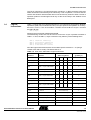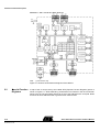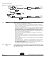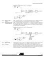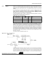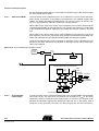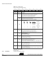
1
Atmel 8051 Microcontrollers Hardware Manual Section 1 The C51 Instruction Set ........................................................................ 1-1 1.1 1.2 Program Status Word................................................................................1-1 Addressing Modes ....................................................................................1-2 1.2.1 Direct Addressing ..............................................................................1-2 1.2.2 Indirect Addressing............................................................................1-2 1.2.3 Register Instructions ...........................................................................1-2 1.2.4 Register-specific Instructions..............................................................1-2 1.2.5 Immediate Constants..........................................................................1-3 1.2.6 Indexed Addressing...........................................................................1-3 1.3 1.4 1.5 Arithmetic Instructions...............................................................................1-4 Logical Instructions ...................................................................................1-5 Data Transfers .........................................................................................1-6 1.5.1 1.6 1.7 1.8 Internal RAM......................................................................................1-6 External RAM ...........................................................................................1-9 Lookup Tables .........................................................................................1-9 Boolean Instructions ...............................................................................1-10 1.8.1 Relative Offset ..................................................................................1-11 1.9 Jump Instructions ....................................................................................1-11 1.10 Instruction Table .....................................................................................1-13 Section 2 Common Features Description ........................................................... 2-16 2.1 2.2 Introduction ............................................................................................2-16 Special Function Registers .....................................................................2-17 2.2.1 Accumulator......................................................................................2-18 2.2.2 B Register.........................................................................................2-18 2.2.3 Program Status Word .......................................................................2-18 2.2.4 Stack Pointer ....................................................................................2-19 2.2.5 Data Pointer......................................................................................2-19 2.2.6 Ports 0 to 3 .......................................................................................2-19 2.2.7 Serial Data Buffer .............................................................................2-19 2.2.8 Timer Registers ................................................................................2-19 2.2.9 Capture Registers.............................................................................2-19 2.2.10 Control Registers.............................................................................2-20 2.3 Oscillator and Clock Circuit .....................................................................2-20 2.3.1 2.4 More about the On-chip Oscillator ....................................................2-20 CPU Timing.............................................................................................2-21 2.4.1 X1 Mode (Standard Mode) ...............................................................2-21 2.4.2 X2 Mode ...........................................................................................2-22 Atmel 8051 Microcontrollers Hardware Manual 1 4316A–8051–01/04 Table of Contents 2.5 Port Structures and Operation ................................................................2-23 2.5.1 I/O Configurations............................................................................2-23 2.5.2 Writing to a Port...............................................................................2-24 2.5.3 Port Loading and Interfacing ............................................................2-26 2.5.4 Read-Modify-Write Feature ..............................................................2-26 2.6 2.7 2.8 Accessing External Memory ...................................................................2-27 PSEN ......................................................................................................2-28 ALE .........................................................................................................2-28 2.8.1 Overlapping External Program and Data Memory Spaces...............2-29 2.8.2 ALE Disable Mode............................................................................2-29 2.9 Timer/Counters .......................................................................................2-30 2.9.1 Timer/Counter Operations ................................................................2-30 2.10 Timer 0....................................................................................................2-30 2.10.1 Mode 0 (13-bit Timer) .......................................................................2-31 2.10.2 Mode 1 (16-bit Timer) .......................................................................2-31 2.10.3 Mode 2 (8-bit Timer with Auto-Reload).............................................2-32 2.10.4 Mode 3 (Two 8-bit Timers) ...............................................................2-32 2.11 Timer 1....................................................................................................2-32 2.11.1 Mode 0 (13-bit Timer) .......................................................................2-33 2.11.2 Mode 1 (16-bit Timer) .......................................................................2-34 2.11.3 Mode 2 (8-bit Timer with Auto Reload).............................................2-34 2.11.4 Mode 3 (Halt)....................................................................................2-34 2.11.5 Interrupt ............................................................................................2-34 2.11.6 Timer Registers ................................................................................2-35 2.12 Timer 2....................................................................................................2-38 2.12.1 Introduction.......................................................................................2-38 2.12.2 Auto-reload Mode .............................................................................2-39 2.12.3 Programmable Clock-output.............................................................2-39 2.12.4 Timer Registers ................................................................................2-41 2.13 Serial Interface........................................................................................2-43 2.13.1 Baud Rates.......................................................................................2-45 2.13.2 Baud Rate Selection Table for UART...............................................2-46 2.13.3 Internal Baud Rate Generator (BRG) ...............................................2-46 2.13.4 Using Timer 1 to Generate Baud Rates ...........................................2-48 2.13.5 Using Timer 2 to Generate Baud Rates ...........................................2-48 2.13.6 More About Mode 0 ..........................................................................2-50 2.13.7 More About Mode 1 ..........................................................................2-51 2.14 Framing Error Detection..........................................................................2-53 2.15 Automatic Address Recognition ..............................................................2-54 2 4316A–8051–01/04 Atmel 8051 Microcontrollers Hardware Manual Table of Contents 2.15.1 Multiprocessor Communications ......................................................2-54 2.15.2 Given Address ..................................................................................2-54 2.15.3 Broadcast Address ...........................................................................2-55 2.15.4 Reset Addresses ..............................................................................2-55 2.16 Interrupts .................................................................................................2-61 2.16.1 How Interrupts Are Handled .............................................................2-62 2.16.2 External Interrupts ............................................................................2-63 2.16.3 Response Time ................................................................................2-63 Atmel 8051 Microcontrollers Hardware Manual 3 4316A–8051–01/04 Section 1 The 8051 Instruction Set The 8051 instruction set is optimized for 8-bit control applications. It provides a variety of fast addressing modes for accessing the internal RAM to facilitate byte operations on small data structures. The instruction set provides extensive support for one-bit variables as a separate data type, allowing direct bit manipulation in control and logic systems that require Boolean processing. An overview of the 8051 instruction set is presented below, with a brief description of how certain instructions might be used. 1.1 Program Status Word The Program Status Word (PSW) contains several status bits that reflect the current state of the CPU. The PSW, shown in Table 1-1 on page 2, resides in SFR space. It contains the Carry bit, the Auxiliary Carry (for BCD operations), the two register bank select bits, the Overflow flag, a parity bit, and two user-definable status flags. The Carry bit, other than serving the functions of a Carry bit in arithmetic operations, also serves as the “Accumulator” for a number of Boolean operations. The bits RS0 and RS1 are used to select one of the four register banks shown below. A number of instructions refer to these RAM locations as R0 through R7. The selection of which of the four banks is being referred to is made on the basis of the bits RS0 and RS1 at execution time. The parity bit reflects the number of 1’s in the Accumulator: P = 1 if the Accumulator contains an odd number of 1’s, and P = 0 if the Accumulator contains an even number of 1’s. Thus the number of 1’s in the Accumulator plus P is always even. Two bits in the PSW are uncommitted and may be used as general purpose status flags. The PSW register contains program status information as detailed in Table 1-1. Atmel 8051 Microcontrollers Hardware Manual 1-1 Rev. 4316A–8051–01/04 The 8051 Instruction Set Table 1-1. PSW: Program Status Word Register (MSB) (LSB) CY AC F0 RS1 RS0 OV - Symbol Position CY PSW.7 Carry flag AC PSW.6 Auxiliary Carry flag. (For BCD operations.) F0 PSW.5 Flag 0 (Available to the user for general purposes.) P Name and Significance Register bank Select control bits 1 & 0. Set/cleared by software to determine working register bank (see Note). RS1 PSW.4 RS0 PSW.3 OV PSW.2 Overflow flag. - PSW.1 (reserved) P PSW.0 Parity flag. Set/cleared by hardware each instruction cycle to indicate and odd/even number of “one” bits in the accumulator, i.e., even parity. Note: The contents of (RS1, RS0) enable the working register banks as follows: (0.0)-Bank 0(00H-07H) (0.1)-Bank 1(08H-0FH) (1.0)-Bank 2(10H-17H) (1.1)-Bank 3(18H-1FH) 1.2 Addressing Modes The addressing modes in the 8051 instruction set are as follows: 1.2.1 Direct Addressing In direct addressing the operand is specified by an 8-bit address field in the instruction. Only 128 Lowest bytes of internal Data RAM and SFRs can be directly addressed. 1.2.2 Indirect Addressing In indirect addressing the instruction specifies a register which contains the address of the operand. Both internal and external RAM can be indirectly addressed. The address register for 8-bit addresses can be R0 or R1 of the selected register bank, or the Stack Pointer. The address register for 16-bit addresses can only be the 16-bit “data pointer” register, DPTR. 1.2.3 Register Instructions The register banks, containing registers R0 through R7, can be accessed by certain instructions which carry a 3-bit register specification within the opcode of the instruction. Instructions that access the registers this way are code efficient, since this mode eliminates an address byte. When the instruction is executed, one of the eight registers in the selected bank is accessed. One of four banks is selected at execution time by the two bank select bits in the PSW. 1.2.4 Register-specific Instructions Some instructions are specific to a certain register. For example, some instructions always operate on the Accumulator, or Data Pointer, etc., so no address byte is needed 1-2 4316A–8051–01/04 Atmel 8051 Microcontrollers Hardware Manual The 8051 Instruction Set to point to it. The opcode does this itself. Instructions that refer to the Accumulator as ‘A’ assemble as accumulator-specific opcodes. 1.2.5 Immediate Constants The value of a constant can follow the opcode in Program Memory. For example; MOV A, # 100 loads the Accumulator with the decimal number 100. The same number could be specified in hex digits as 64H. 1.2.6 Indexed Addressing Only Program Memory can be accessed with indexed addressing, and it can only be read. This addressing mode is intended for reading look-up tables in Program Memory. A 16-bit base register (either DPTR or the Program Counter) points to the base of the table, and the Accumulator is set up with the table entry number. The address of the table entry in Program Memory is formed by adding the Accumulator data to the base pointer. Another type of indexed addressing is used in the “case jump” instruction. In this case the destination address of a jump instruction is computed as the sum of the base pointer and the Accumulator data. Atmel 8051 Microcontrollers Hardware Manual 1-3 4316A–8051–01/04 The 8051 Instruction Set 1.3 Arithmetic Instructions The menu of arithmetic instructions is listed in Table 1-2. The table indicates the addressing modes that can be used with each instruction to access the <byte> operand. For example, the ADD A, <byte> instruction can be written as: ADD ADD ADD ADD A,7FH (direct addressing) A,@ R0(indirect addressing) A,R7 (register addressing) A,# 127(immediate constant) Table 1-2. A list of the Atmel 8051 Arithmetic Instructions. Mnemonic Operation Execution Time in X1 Mode @12 MHz (µs) Addressing Modes Dir Ind Reg Im m ADD A, <byt>e A = A + <byte> X X X X ADDC A, <byte> A = A + <byte> + C X X X X 1 SUBB A, <byte> A = A – <byte> – C X X X X 1 INC A A=A+1 Accumulator only 1 INC <byte> <byte> = <byte> + 1 X X 1 INC DPTR DPTR = DPTR + 1 Data Pointer only 2 DEC A A=A–1 Accumulator only 1 DEC <byte> <byte> = <byte> – 1 X 1 MUL AB B:A = B × A ACC and B only 4 DIV AB A = Int [A/B] B = Mod [A/B] ACC and B only 4 DA A Decimal Adjust Accumulator only 1 X X X The execution times listed in Table 1-2 assume a 12 MHz clock frequency and X1 mode. All of the arithmetic instructions execute in 1 µs except the INC DPTR instruction, which takes 2 µs, and the Multiply and Divide instructions, which take 4 µs. Note that any byte in the internal Data Memory space can be incremented or decremented without going through the Accumulator. One of the INC instructions operates on the 16-bit Data Pointer. The Data Pointer is used to generate 16-bit addresses for external memory, so being able to increment it in one 16-bit operation is a useful feature. The MUL AB instruction multiplies the Accumulator by the data in the B register and puts the 16-bit product into the concatenated B and Accumulator registers. The DIV AB instruction divides the Accumulator by the data in the B register and leaves the 8-bit quotient in the Accumulator, and the 8-bit remainder in the B register. Oddly enough, DIV AB finds less use in arithmetic “divide” routines than in radix conversions and programmable shift operations. An example of the use of DIV AB in a radix conversion will be given later. In shift operations, dividing a number by 2n shifts its n bits to the right. Using DIV AB to perform the division completes the shift in 4 µs leaves the B register holding the bits that were shifted out. 1-4 4316A–8051–01/04 Atmel 8051 Microcontrollers Hardware Manual The 8051 Instruction Set The DA A instruction is for BCD arithmetic operations. In BCD arithmetic ADD and ADDC instructions should always be followed by a DA A operation, to ensure that the result is also in BCD. Note that DAA will not convert a binary number to BCD. The DA A operation produces a meaningful result only as the second step in the addition of two BCD bytes. 1.4 Logical Instructions Table 1-3 shows the list of logical instructions. The instructions that perform Boolean operations (AND, OR, Exclusive OR, NOT) on bytes perform the operation on a bit-bybit basis. That is, if the Accumulator contains 00110101B and <byte> contains 01010011B, then ANL A,<byte> will leave the Accumulator holding 00010001B. The addressing modes that can be used to access the <byte> operand are listed in Table 1-3. Thus, the ANL A, <byte> instruction may take any of the following forms. ANL ANL ANL ANL A, A, A, A, 7FH(direct addressing) @ R1(indirect addressing) R6(register addressing) # 53H(immediate constant) All of the logical instructions that are Accumulator specific execute in 1 µs (using a 12 MHz clock and X1 mode). The others take 2 µs. Table 1-3. A list of the Atmel 8051 Logical Instructions Mnemonic Operation Execution Time @ 12MHz (µs) Addressing Modes Dir Ind Reg Imm X X X ANL A, <byte> A = A AND <byte> X ANL <byte>, A <byte> = <byte> AND A X 1 ANL <byte>, # data <byte> = <byte> AND # data X 2 ORL A, <byte> A = A OR <byte> X ORL <byte>, A <byte> = <byte> OR A X 1 ORL <byte>, # data <byte> = <byte> OR # data X 2 XRL A, <byte> A = A XOR <byte> X XRL <byte>, A <byte> = <byte> XOR A X 1 XRL <byte>, # data <byte> = <byte> XOR # data X 2 CLR A A = 00H Accumulator only 1 CLP A A = NOT A Accumulator only 1 RL A Rotate ACC Left 1 bit Accumulator only 1 RLC A Rotate Left through Carry Accumulator only 1 RR A Rotate ACC Right 1 bit Accumulator only 1 RRC A Rotate Right through Carry Accumulator only 1 SWAP A Swap Nibbles in A Accumulator only 1 Atmel 8051 Microcontrollers Hardware Manual X X X X X X 1 1 1 1-5 4316A–8051–01/04 The 8051 Instruction Set Note that Boolean operations can be performed on any byte in the internal Data Memory space without going through the Accumulator. The XRL <byte>, # data instruction, for example, offers a quick and easy way to invert port bits, as in XRL P1, #OFFH If the operation is in response to an interrupt, not using the Accumulator saves the time and effort to stack it in the service routine. The Rotate instructions (RL A, RLC A, etc.) shift the Accumulator 1 bit to the left or right. For a left rotation, the MSB rolls into the LSB position. For a right rotation, the LSB rolls into the MSB position. The SWAP A instruction interchanges the high and low nibbles within the Accumulator. this is a useful operation in BCD manipulations. For example, if the Accumulator contains a binary number which is known to be less than 100, it can be quickly converted to BCD by the following code: MOV B, #10 DIV AB SWAP A ADD A,B Dividing the number by 10 leaves the tens digit in the low nibble of the Accumulator, and the ones digit in the B register. The SWAP and ADD instructions move the tens digit to the high nibble of the Accumulator, and the ones digit to the low nibble. 1.5 Data Transfers 1.5.1 Internal RAM Table 1-4 shows the menu of instructions that are available for moving data around within the internal memory spaces, and the addressing modes that can be used with each one. With a 12 MHz clock and X1 mode, all of these instructions execute in either 1 or 2 µs. The MOV <dest>, <src> instruction allows data to be transferred between any two internal RAM or SFR locations without going through the Accumulator. Remember the Upper 128 bytes of data RAM can be accessed only by indirect, and SFR space only by direct addressing. Note that in all 8051 devices, the stack resides in on-chip RAM, and grows upwards. The PUSH instruction first increments the Stack Pointer (SP), then copies the byte into the stack. PUSH and POP use only direct addressing to identify the byte being saved or restored, but the stack itself is accessed by indirect addressing using the SP register. 1-6 4316A–8051–01/04 Atmel 8051 Microcontrollers Hardware Manual The 8051 Instruction Set This means the stack can go into the Upper 128, if they are implemented, but not into SFR space. Table 1-4. Atmel 8051 Data Transfer Instructions that Access Internal Data Memory Space Mnemonic Operation Execution Time @ 12MHz (µs) Addressing Modes Dir Ind Reg Imm X MOV A, <src> A = <src> X X X MOV <dest>, A <dest> = A X X X MOV <dest>, <src> <dest> = <src> X X X MOV DPTR, # data 16 DPTR = 16-bit immediate constant PUSH <src> INC SP: MOV “@SP”, <scr> X 2 POP <dest> MOV <dest>, “@SP”: DEC SP X 2 XCH A, <byte> ACC and <byte> Exchange Data X XCHD A, @Ri ACC and @ Ri exchange low nibbles X X X 1 1 X 2 X 2 1 1 The Upper 128 are not implemented in the 8 standard 8051, nor in their ROMless. With these devices, if the SP points to the Upper 128 PUSHed bytes are lost, and POPped bytes are indeterminate. The Data Transfer instructions include a 16-bit MOV that can be used to initialize the Data Pointer (DPTR) for look-up tables in Program Memory, or for 16-bit external Data Memory accesses. The XCH A, <byte> instruction causes the Accumulator and addressed byte to exchange data. The XCHD A, @ Ri instruction is similar, but only the low nibbles are involved in the exchange. The see how XCH and XCHD can be used to facilitate data manipulations, consider first the problem of shifting an 8-digit BCD number two digits to the right. Table 1-5 shows how this can be done using direct MOVs, and for comparison how it can be done using XCH instructions. To aid in understanding how the code works, the contents of the registers that are holding the BCD number and the content of the Accumulator are shown alongside each instruction to indicate their status after the instruction has been executed. After the routine has been executed, the Accumulator contains the two digits that were shifted out on the right. Performing the routine with direct MOVs uses 14 code bytes and 9 µs of execution time (assuming a 12 MHz clock and X1 mode). The same operation with XCHs uses less code and executes almost twice as fast. Atmel 8051 Microcontrollers Hardware Manual 1-7 4316A–8051–01/04 The 8051 Instruction Set Table 1-5. Shifting a BCD Number Two Digits to the Right MOV A,2EH MOV 2EH, 2DH MOV 2DH, 2CH MOV 2CH, 2BH MOV 2BH, # 0 Note: 2B 2C 2D 2E ACC 00 00 00 00 00 12 12 12 12 00 34 34 34 12 12 56 56 34 34 34 78 56 56 56 56 78 78 78 78 78 2A 2B 2C 2E 2E ACC 00 00 00 00 00 12 00 00 00 00 34 34 12 12 12 56 56 56 34 34 78 78 78 78 56 00 12 34 56 78 Using direct MOVs: 14 bytes, 9 µs CLR A XCH A,2BH XCH A,2CH XCH A,2DH XCH A,2EH Note: 2A Using XCHs: 9 bytes, 5 µs Table 1-6. Shifting a BCD Number One Digit to the Right 2A 2B 2C 2D 2E ACC MOV R1,# 2EH 00 12 34 56 78 XX MOV R0, # 2DH 00 12 34 56 78 XX LOOP: MOV A, @R1 00 12 34 56 78 78 XCHD A, @R0 00 12 34 58 78 76 SWAP A 00 12 34 58 78 67 MOV @R1, A 00 12 34 58 67 67 DEC R1 00 12 34 58 67 67 DEC R0 00 12 34 58 67 67 loop for R1 = 2DH: 00 12 38 45 67 45 loop for R1 = 2CH: 00 18 23 45 67 23 loop for R1 = 2BH: 08 01 23 45 67 01 CLR A 08 01 23 45 67 00 XCH A,2AH 00 01 23 45 67 08 loop for R1 = 2EH: CJNE R1, #2AH, LOOP To right-shift by an odd number of digits, a one-digit shift must be executed. Table 1-6 shows a sample of code that will right-shift a BCD number one digit, using the XCHD instruction. Again, the contents of the registers holding the number and of the Accumulator are shown alongside each instruction. First, pointers R1 and R0 are set up to point to the two bytes containing the last four BCD digits. Then a loop is executed which leaves the last byte, location 2EH, holding the last two digits of the shifted number. The pointers are decremented, and the loop is 1-8 4316A–8051–01/04 Atmel 8051 Microcontrollers Hardware Manual The 8051 Instruction Set repeated for location 2DH. The CJNE instruction (Compare and Jump if Not Equal) is a loop control that will be described later. The loop is executed from LOOP to CJNE for R1 = 2EH, 2DH, 2CH and 2BH. At that point the digit that was originally shifted out on the right has propagated to location 2AH. Since that location should be left with 0s, the lost digit is moved to the Accumulator. 1.6 External RAM Table 1-7 shows a list of the Data Transfer instructions that access external Data Memory. Only indirect addressing can be used. The choice is whether to use a one-byte address, @Ri, where Ri can be either R0 or R1 of the selected register bank, or a twobyte address, @DPTR. The disadvantage to using 16-bit addresses if only a few Kbytes of external RAM are involved is that 16-bit addresses use all 8 bits of Port 2 as address bus. On the other hand, 8-bit addresses allow one to address a few Kbytes of RAM, as shown in Table 1-7, without having to sacrifice all of Port 2. All of these instructions execute in 2 µs, with a 12 MHz clock (and X1 mode). Note that in all external Data RAM accesses, the Accumulator is always either the destination or source of the data. The read and write strobes to external RAM are activated only during the execution of a MOVX instruction. Separately these signals are inactive, and in fact if they’re not going to be used at all, their pins are available as extra I/O lines. Table 1-7. Data Transfer Instructions that Access External Data Memory Space 1.7 Lookup Tables Execution Time @ 12MHz (µs) Address Width Mnemonic Operation 8 bits MOVX A, @Ri Read external RAM @ Ri 2 8 bits MOVX @ Ri, A Write external RAM @ Ri 2 16 bits MOVX A, @ DPTR Read external RAM @ DPTR 2 16 bits MOVX @ DPTR, A Write external RAM @ DPTR 2 Table 1-8 shows the two instructions that are available for reading lookup tables in Program Memory. Since these instructions access only Program Memory, the lookup tables can be read, not updated. The mnemonic is MOVC for “move constant”. If the table access is to external Program Memory, then the read strobe is PSEN. The first MOVC instruction in Table 1-8 can accommodate a table of up to 256 entries, numbered 0 through 255. The number of the desired entry is loaded into the Accumulator, and the Data Pointer is set up to point to beginning of the table. Then MOVC A, @A + DPTR copies the desired table entry into the Accumulator. The other MOVC instruction works the same way, except the Program Counter (PC) is used as the table base, and the table is accessed through a subroutine. First the number of the desired entry is loaded into the Accumulator, and the subroutine is called: Atmel 8051 Microcontrollers Hardware Manual 1-9 4316A–8051–01/04 The 8051 Instruction Set MOV A, ENTRY_NUMBER CALLTABLE The subroutine “TABLE” would look like this: TABLE:MOVC A, @A + PC RET The table itself immediately follows the RET (return) instruction in Program Memory. This type of table can have up to 255 entries, numbered 1 through 255. Number 0 cannot be used, because at the time the MOVC instruction is executed, the PC contains the address of the RET instruction. An entry numbered 0 would be the RET opcode itself. Table 1-8. Lookup Table Read Instructions 1.8 Boolean Instructions Mnemonic Operation Execution Time @ 12MHz (µs) MOVC A, @A + DPTR Read Pgm Memory at (A + DPTR) 2 MOVC A, @A + PC Read Pgm Memory at (A + PC) 2 8051 devices contain a complete Boolean (single-bit) processor. The internal RAM contains 128 addressable bits, and the SFR space can support up to 128 other addressable bits. All of the port lines are bit-addressable, and each one can be treated as a separate single-bit port. The instructions that access these bits are not just conditional branches, but a complete menu of move, set, clear, complement, OR and AND instructions. These kinds of bit operations are not easily obtained in other architectures with any amount of byte-oriented software. The instruction set for the Boolean processor is shown in Table 1-9. All bit accesses are by direct addressing. Bit addresses 00H through 7FH are in the Lower 128, and bit addresses 80H through FFH are in SFR space. Table 1-9. 8051 Boolean Instructions Mnemonic Operation Execution Time @ 12MHz (µs) ANL C,bit ANL C,/bit ORL C,bit ORL C,/bit MOV C,bit MOV bit,C CLR C CLR bit SETB C SETB bit CPL C CPL bit JC rel JNC rel JB bit,rel JNB bit,rel JBC bit,rel C = C AND bit C = C AND (NOT bit) C = C OR bit C = C OR (NOT bit) C = bit bit = C C=0 bit = 0 C=1 bit = 1 C = NOT C bit = NOT bit Jump if C = 1 Jump if C = 0 Jump if bit = 1 Jump if bit = 0 Jump if bit = 1 ; CLR bit 2 2 2 2 1 2 1 1 1 1 1 1 2 2 2 2 2 Note how easily an internal flag can be moved to a port pin: MOV C, FLAG MOV P1.0, C 1-10 4316A–8051–01/04 Atmel 8051 Microcontrollers Hardware Manual The 8051 Instruction Set In this example, FLAG is the name of any addressable bit in the lower 128 or SFR space. An I/O line (the LSB of Port 1, in the case) is set or cleared depending on whether the flag bit is 1 or 0. The Carry bit in the PSW is used as the single-bit Accumulator of the Boolean processor. Bit instructions that refer to the Carry bit as C assemble as Carry-specific instructions (CLR C, etc.). The Carry bit also has a direct address, since it resides in the PSW register, which is bit-addressable. Note that the Boolean instruction set includes ANL and ORL operations, but not the XRL (Exclusive OR) operation. An XRL operation is simple to implement in software. Suppose, for example, it is required to form the Exclusive OR of two bits: C= bit1 XRL bit2 The software to do that could be as follows: MOV C, bit1 JNB bit2, OVER CPL C OVER: (continue) First, bit 1 is moved to the Carry. If bit 2 = 0, then C now contains the correct result. That is, bit 1 XRL bit2 = bit1 if bit2 = 0. On the other hand, if bit2 = 1 C now contains the complement of the correct result. It need only be inverted (CPL C) to complete the operation. This code uses the JNB instruction, one of a series of bit-test instructions which execute a jump if the addressed bit is set (JC, JB, JBC) or if the addressed bit is not set (JNC, JNB). In the above case, bit2 is being tested, and if bit2 = 0 the CPL C instruction is jumped over. JBC executes the jump if the addressed bit is set, and also clears the bit. Thus a flag can be tested and cleared in one operation. All the PSW bits are directly addressable, so the Parity bit, or the general purpose flags, for example, are also available to the bit-test instructions. 1.8.1 Relative Offset The destination address for these jumps is specified to the assembler by a label or by an actual address in Program Memory. However, the destination address assembles to a relative offset byte. This is a signed (two’s complement) offset byte which is added to the PC in two’s complement arithmetic if the jump is executed. The range of the jump is therefore -128 to +127 Program Memory bytes relative to the first byte following the instruction. 1.9 Jump Instructions Table 1-10 shows the list of unconditional jumps. Table 1-10. Unconditional Jumps in Atmel 8051 Mnemonic Operation Execution Time @ 12MHz (µs) JMP addr JMP @A + DPTR CALL addr RET RETI NOP Jump to addr Jump to A + DPTR Call subroutine at addr Return from subroutine Return from interrupt No operation 2 2 2 2 2 1 The table lists a single “JMP addr” instruction, but in fact there are three -SJMP, LJMP, AJMP -which differ in the format of the destination address. JMP is a generic mnemonic which can be used if the programmer does not care how the jump is encoded. Atmel 8051 Microcontrollers Hardware Manual 1-11 4316A–8051–01/04 The 8051 Instruction Set The SJMP instruction encodes the destination address as relative offset, as described above. The instruction is 2 bytes long, consisting of the opcode and the relative offset byte. The jump distance is limited to range of -128 to + 127 bytes relative to the instruction following the SJMP. The LJMP instruction encodes the destination address as a 16-bit constant. The instruction is 3 bytes long, consisting of the opcode and two address bytes. The destination address can be anywhere in the 64K Program Memory space. The AJMP instruction encodes the destination address as an 11-bit constant. The instruction is 2 bytes long, consisting of the opcode, which itself contains 3 of the 11 address bits, followed by another byte containing the low 8 bits of the destination address. When the instruction is executed, these 11 bits are simply substituted for the low 11 bits in the PC. The high 5 bits stay the same. Hence the destination has to be within the same 2K block as the instruction following the AJMP. In all cases the programmer specifies the destination address to the assembler in the same way: as a label or as a 16-bit constant. The assembler will put the destination address into the correct format for the given instruction. If the format required by the instruction will not support the distance to the specified destination address, a “Destination out of range” message is written, into the list file. The JMP @ A + DPTR instruction supports case jumps. The destination address is computed at execution time as the sum of the 16-bit DPTR register and the Accumulator. Typically, DPTR is set up with the address of a jump table, and the Accumulator is given an index to the table. In a 5-way branch, for example, an integer 0 through 4 is loaded into the Accumulator. The code to be executed might be as follows: MOV MOV RL JMP DPTR, # JUMP_TABLE A, INDEX_NUMBER A @ A + DPTR The RLA instruction converts the index number (0 through 4) to an even number on the range 0 through 8, because each entry in the jump table is 2 bytes long: JUMP_TABLE: AJMP CASE_0 AJMP CASE_1 AJMP CASE_2 AJMP CASE_3 AJMP CASE_4 Table 1-10 shows a single “CALL addr” instruction, but there are two of them -LCALL and ACALL -which differ in the format in which the subroutine address is given to the CPU. CALL is a generic mnemonic which can be used if the programmer does not care which way the address is encoded. The LCALL instruction uses the 16-bit address format, and the subroutine can be anywhere in the 64K Program Memory space. The ACALL instruction uses the 11-bit format, and the subroutine must be in the same 2K block as the instruction following the ACALL. In any case the programmer specifies the subroutine address to the assembler in the same way: as a label or as a 16-bit constant. The assembler will put the address into the correct format for the given instructions. Subroutines should end a RET instruction, which returns execution following the CALL. RETI is used to return from an interrupt service routine. The only difference between RET and RETI is that RETI tells the interrupt control system that the interrupt in progress is 1-12 4316A–8051–01/04 Atmel 8051 Microcontrollers Hardware Manual The 8051 Instruction Set done. If there is no interrupt in progress at the time RETI is executed, then the RETI is functionally identical to RET. Table 1-11 shows the list of conditional jumps available to the Atmel 8051 user. All of these jumps specify the destination address by the relative offset method, and so are limited to a jump distance of -128 to + 127 bytes from the instruction following the conditional jump instruction. Important to note, however, the user specifies to the assembler the actual destination address the same way as the other jumps: as a label or a 16-bit constant. Table 1-11. Conditional Jumps in Atmel 8051 Devices Mnemonic Operation Execution Time @ 12MHz (µs) Addressing Modes DIR IND REG IMM JZ rel Jump if A = 0 Accumulator only 2 JNZ rel Jump if A ≠ 0 Accumulator only 2 DJNZ <byte>,rel Decrement and jump if not zero X CJNZ A,<byte>,rel Jump if A = <byte> X CJNE <byte>,#data,rel Jump if <byte> = #data X 2 X X X 2 2 There is no Zero bit in the PSW. The JZ and JNZ instructions test the Accumulator data for that condition. The DJNZ instruction (Decrement and Jump if Not Zero) is for loop control. To execute a loop N times, load a counter byte with N and terminate the loop with DJNZ to the beginning of the loop, as shown below for N = 10: MOV COUNTER, # 10 LOOP:(begin loop) * * * (end loop) DJNZ COUNTER, LOOP (continue) The CJNE instruction (Compare and Jump if Not Equal) can also be used for loop control as in Table 1-11. Two bytes are specified in the operand field of the instruction. The jump is executed only if the two bytes are not equal. In the example of Figure 12, the two bytes were the data in R1 and the constant 2AH. The initial data in R1 was 2EH. Every time the loop was executed, R1 was decremented, and the looping was to continue until the R1 data reached 2AH. Another application of this instruction is in “greater than, less than” comparisons. The two bytes in the operand field are taken as unsigned integers. If the first is less than the second, then the Carry bit is set (1). If the first is greater than or equal to the second, then the Carry bit is cleared. 1.10 Instruction Table Table 1-12 shows the Hex value of each instruction detailing the: byte size number of cycles flags modified by the instruction Atmel 8051 Microcontrollers Hardware Manual 1-13 4316A–8051–01/04 1-14 4316A–8051–01/04 MOV A,R0 1-1 MOVX R0,A 1-1 Fx SUBB A,R0 1-1,C,OV,AC 9x Ex MOV dir,R0 2-2 8x DJNZ R0,rel 2-2 MOV R0,#imm 2-1 7x Dx XRL A,R0 1-1 6x XCH A,R0 1-1 ANL A,R0 1-1 5x Cx ORL A,R0 1-1 4x CJNE R0,#imm,rel 3-2,C ADDC A,R0 1-1,C,OV,AC 3x Bx ADD A,R0 1-1,C,OV,AC 2x MOV R0,dir 2-2 DEC R0 1-1 1x Ax INC R0 1-1 Ox x8 MOVX R1,A 1-1 MOV A,R1 1-1 DJNZ R1,rel 2-2 XCH A,R1 1-1 CJNE R1,#imm,rel 3-2,C MOV R1,dir 2-2 SUBB A,R1 1-1,C,OV,AC MOV dir,R1 2-2 MOV R1,#imm 2-1 XRL A,R1 1-1 ANL A,R1 1-1 ORL A,R1 1-1 ADDC A,R1 1-1,C,OV,AC ADD A,R1 1-1,C,OV,AC DEC R1 1-1 INVC R1 1-1 x9 MOVX R2,A 1-1 MOV A,R2 1-1 DJNZ R2,rel 2-2 XCH A,R2 1-1 CJNE R2,#imm,rel 3-2,C MOV R2,dir 2-2 SUBB A,R2 1-1,C,OV,AC MOV dir,R2 2-2 MOV R2,#imm 2-1 XRL A,R2 1-1 ANL A,R2 1-1 ORL A,R2 1-1 ADDC A,R2 1-1,C,OV,AC ADD A,R2 1-1,C,OV,AC DEC R2 1-1 INC R2 1-1 xA MOVX R3,A 1-1 MOV A,R3 1-1 DJNZ R3,rel 2-2 XCH A,R3 1-1 CJNE R3,#imm,rel 3-2,C MOV R3,dir 2-2 SUBB A,R3 1-1,C,OV,AC MOV dir,R3 2-2 MOV R3,#imm 2-1 XRL A,R3 1-1 ANL A,R3 1-1 ORL A,R3 1-1 ADDC A,R3 1-1,C,OV,AC ADD A,R3 1-1,C,OV,AC DEC R3 1-1 INC R3 1-1 xB MOVX R4,A 1-1 MOV A,R4 1-1 DJNZ R4,rel 2-2 XCH A,R4 1-1 CJNE R4,#imm,rel 3-2,C MOV R4,dir 2-2 SUBB A,R4 1-1,C,OV,AC MOV dir,R4 2-2 MOV R4,#imm 2-1 XRL A,R4 1-1 ANL A,R4 1-1 ORL A,R4 1-1 ADDC A,R4 1-1,C,OV,AC ADD A,R4 1-1,C,OV,AC DEC R4 1-1 INC R4 1-1 xC MOVX R5,A 1-1 MOV A,R5 1-1 DJNZ R5,rel 2-2 XCH A,R5 1-1 CJNE R5,#imm,rel 3-2,C MOV R5,dir 2-2 SUBB A,R5 1-1,C,OV,AC MOV dir,R5 2-2 MOV R5,#imm 2-1 XRL A,R5 1-1 ANL A,R5 1-1 ORL A,R5 1-1 ADDC A,R5 1-1,C,OV,AC ADD A,R5 1-1,C,OV,AC DEC R5 1-1 INC R5 1-1 xD MOVX R6,A 1-1 MOV A,R6 1-1 DJNZ R6,rel 2-2 XCH A,R6 1-1 CJNE R6,#imm,rel 3-2,C MOV R6,dir 2-2 SUBB A,R6 1-1,C,OV,AC MOV dir,R6 2-2 MOV R6,#imm 2-1 XRL A,R6 1-1 ANL A,R6 1-1 ORL A,R6 1-1 ADDC A,R6 1-1,C,OV,AC ADD A,R6 1-1,C,OV,AC DEC R6 1-1 INC R6 1-1 xE MOVX R7,A 1-1 MOV A,R7 1-1 DJNZ R7,rel 2-2 XCH A,R7 1-1 CJNE R7,#imm,rel 3-2,C MOV R7,dir 2-2 SUBB A,R7 1-1,C,OV,AC MOV dir,R7 2-2 MOV R7,#imm 2-1 XRL A,R7 1-1 ANL A,R7 1-1 ORL A,R7 1-1 ADDC A,R7 1-1,C,OV,AC ADD A,R7 1-1,C,OV,AC DEC R7 1-1 INC R7 1-1 xF The 8051 Instruction Set Table 1-12. 8051 Instruction Table Atmel 8051 Microcontrollers Hardware Manual NOP 1-1 JBC bit,rel 3-2 JB bit,rel 3-2 JNB bit,rel 3-2 JC rel 2-2 JNC rel 2-2 JZ rel 2-2 JNZ rel 2-2 SJMP rel 2-2 MOV DPTR,#imm16 3-2 ORL C,/bit 2-2,C ANL C,/bit 2-2,C PUSH dir 2-2 POP dir 2-2 MOVX A,@DPTR 1-2 MOVX @DPTR,A 1-2 Ox 1x 2x 3x 4x 5x 6x 7x 8x 9x Ax Bx Cx Dx Ex Fx x0 Atmel 8051 Microcontrollers Hardware Manual ACALL addr11 2-2 AJMP addr11 2-2 ACALL addr11 2-2 AJMP addr11 2-2 ACALL addr11 2-2 AJMP addr11 2-2 ACALL addr11 2-2 AJMP addr11 2-2 ACALL addr11 2-2 AJMP addr11 2-2 ACALL addr11 2-2 AJMP addr11 2-2 ACALL addr11 2-2 AJMP addr11 2-2 ACALL addr 2-2 AJMP addr 2-2 x1 MOVX @R0,A 1-2 MOVX A,@R0 1-2 SETB bit 2-1 CLR bit 2-1 CPL bit 2-1 MOV C,bit 2-1,C MOV bit,C 2-2 ANL C,bit 2-2,C ORL C,bit 2-2,C XRL dir,A 2-1 ANL dir,A 2-1 ORL dir,A 2-1 RETI 1-2 RET 1-2 LCALL code 3-2 LJMP code 3-2 x2 MOVX @R1,A 1-2 MOVX A,@R1 1-2 SETB C 1-1,c=1 CLR C 1-1,C=0 CPL C 1-1,C INC DPTR 1-2 MOVC A,@A+DPTR 1-2 MOVC A,@A+PC 1-2 JMP @A+DPTR 1-2 XRL dir,#imm 3-2 ANL dir,#imm 3-2 ORL dir,#imm 3-2 RLC A 1-1,C RL A 1-1 RRC A 1-1.C RR A 1-1 x3 CPL A 1-1 CLR A 1-1 DA A 1-1,C SWAP A 1-1 CJNE A,#imm,rel 3-2,C MUL AB 1-4,C=0,OV SUBB A,#imm 2-1,C,OV,AC DIV AB 1-4,C=0,OV MOV A,#imm 2-1 XRL A,#imm 2-1 ANL A,#imm 2-1 ORL A,#imm 2-1 ADDC A,#imm 2-1,C,OV,AC ADD A,#imm 2-1,C,OV,AC DEC A 1-1 INC A 1-1 x4 MOV dir,A 2-1 MOV A,dir 2-1 DJNZ dir,rel 3-2 XCH A,dir 2-1 CJNE A,dir,rel 3-2,C SUBB A,dir 2-1,C,OV,AC MOV dir,dir 3-2 MOV dir,#imm 3-2 XRL A,dir 2-1 ANL A,dir 2-1 ORL A,dir 2-1 ADDC A,dir 2-1,C,OV,AC ADD A,dir 2-1,C,OV,AC DEC dir 2-1 INC dir 2-1 x5 MOVX @R0,A 1-1 MOV A,@R0 1-1 XCHD A,@R0 1-1 XCH A,@R0 1-1 CJNE @R0,#imm,rel 3-2,C MOV @R0,dir 2-2 SUBB A,@R0 1-1,C,OV,AC MOV dir,@R0 2-2 MOV @R0,#imm 2-1 XRL A,@R0 1-1 ANL A,@R0 1-1 ORL, A,@R0 1-1 ADDC A,@R0 1-1,C,OV,AC ADD A,@R0 1-1,C,OV,AC DEC @R0 1-1 INC @R0 1-1 x6 MOVX @R1,A 1-1 MOV A,@R1 1-1 XCHD A,@R1 1-1 XCH A,@R1 1-1 CJNE @R1,#imm,rel 3-2,C MOV @R1,dir 2-2 SUBB A,@R1 1-1,C,OV,AC MOV dir,@R1 2-2 MOV @R1,#imm 2-1 XRL A,@R1 1-1 ANL A,@R1 1-1 ORL A,@R1 1-1 ADDC A,@R1 1-1,C,OV,AC ADD A,@R1 1-1,C,OV,AC DEC @R1 1-1 INC @R1 1-1 x7 The 8051 Instruction Set Table 1-12. 8051 Instruction Table (Continued) 1-15 4316A–8051–01/04 Atmel 8051 Microcontrollers Hardware Manual 1-16 Rev. 4316A–8051–01/04 Section 2 Common Features Description 2.1 Introduction This chapter presents a comprehensive description of the on-chip hardware features of the Atmel 8051 microcontrollers. Included in this description are: The port drivers and how they function both as ports and, for Ports 0 and 2, in bus operations The Timer/Counters The serial Interface The Interrupt System Reset The reduced Power Modes Atmel 8051 Microcontrollers Hardware Manual 2-17 Rev. 4316A–8051–01/04 Common Features Description Figure 2-1. 8051 Architecture Block Diagram Note: (*)For Timer 2 only. Figure 2-1 shows a functional block diagram of the 80C51s. 2.2 Special Function Registers 2-18 4316A–8051–01/04 A map of the on-chip memory area called SFR (Special Function Register) space is shown in Figure 2-1. SFRs marked by parentheses are resident in the microcontroller which have the Timer2 feature.Note that not all of the addresses are occupied. Read accesses to these addresses will in general return random data. Atmel 8051 Microcontrollers Hardware Manual Common Features Description Table 2-1. SFR Map Bit Addressable 8 Bytes Non-bit Addressable F8h FFh F0h B F7h E8h EFh E0h ACC E7h D8h DFh D0h PSW C8h (T2CON) D7h (RCAP2L) (RCAP2H) (TL2) (TH2) CFh C0h C7h B8h IP BFh B0h P3 B7h A8h IE AFh A0h P2 A7h 98h SCON 90h P1 88h TCON TMOD TL0 TL1 80h P0 SP DPL DPH 0/8 1/9 2/A 3/B Note: SBUF 9Fh 97h TH0 4/C TH1 5/D AUXR 6/E CKCON 8Fh PCON 87h 7/F Reserved User software should not write to the reserved locations, since they may be used in derivative Atmel 8051 products to invoke new features. The functions of the SFRs are described as below. 2.2.1 Accumulator ACC is the Accumulator register. The mnemonics for accumulator-specific instructions, however, refer to the accumulator simply as A. 2.2.2 B Register The B register is used during multiply and divide operations. For other instructions it can be treated as another scratch pad register. 2.2.3 Program Status Word The PSW register contains program status information as detailed in Table 2-2. Atmel 8051 Microcontrollers Hardware Manual 2-19 4316A–8051–01/04 Common Features Description Table 2-2. PSW: Program Status Word Register (MSB) (LSB) CY AC F0 RS1 RS0 OV - Symbol Position CY PSW.7 Carry flag AC PSW.6 Auxiliary Carry flag. (For BCD operations.) F0 PSW.5 Flag 0 (Available to the user for general purposes.) P Name and Significance Register bank Select control bits 1 & 0. Set/cleared by software to determine working register bank (see Note). RS1 PSW.4 RS0 PSW.3 OV PSW.2 Overflow flag. - PSW.1 (reserved) P PSW.0 Parity flag. Set/cleared by hardware each instruction cycle to indicate and odd/even number of “one” bits in the accumulator, i.e., even parity. Note: The contents of (RS1, RS0) enable the working register banks as follows (0.0)-Bank 0(00H-07H) (0.1)-Bank 1(08H-0FH) (1.0)-Bank 2(10H-17H) (1.1)-Bank 3(18H-1FH) 2.2.4 Stack Pointer The Stack Pointer register is 8 bits wide. It is incremented before data is stored during PUSH and CALL executions. While the stack may reside anywhere in on-chip RAM, the Stack Pointer is initialized to 07H after a reset. This causes the stack to begin at location 08H. 2.2.5 Data Pointer The Data Pointer (DPTR) consists of a high byte (DPH) and a low byte (DPL). Its intended function is to hold a 16-bit address. It may be manipulated as a 16-bit register or as two independent 8-bit registers. 2.2.6 Ports 0 to 3 P0, P1, P2 and P3 are the SFR latches of Ports 0, 1, 2 and 3, respectively. 2.2.7 Serial Data Buffer The Serial Data Buffer is actually two separate registers, a transmit buffer and a receive buffer register. When data is moved to SBUF, it goes to the transmit buffer where it is held for serial transmission. (Moving a byte to SBUF is what initiates the transmission.) When data is moved from SBUF, it comes from the receive buffer. 2.2.8 Timer Registers Register pairs (TH0, TL0), (TH1, TL1), and (TH2, TL2) are the 16-bit counting registers for Timer/Counters 0, 1, and 2, respectively. 2.2.9 Capture Registers The register pair (RCAP2H, RCAP2L) are the capture register for the Timer 2 ‘capture mode’. In this mode, in response to a transition at the 80C52’s T2EX pin, TH2 and TL2 are copied into RCAP2H and RCAP2L. Timer 2 also has a 16-bit auto-reload mode, and RCAP2H and RCAP2L hold the reload value for this mode. More about Timer 2’s features in Section 1.6. 2-20 4316A–8051–01/04 Atmel 8051 Microcontrollers Hardware Manual Common Features Description 2.2.10 Control Registers Special Function Registers IP, IE, TMOD, TCON, T2CON, SCON, and PCON contain control and status bits for the interrupt system, the timer/counters, and the serial port. They are described in later sections. 2.3 Oscillator and Clock Circuit XTAL1 and XTAL2 are the input and output of a single-stage on-chip inverter, which can be configured with off-chip components as a Pierce oscillator, as shown in Figure 2-2. The on-chip circuitry, and selection of off-chip components to configure the oscillator are discussed in Section 1.12. Figure 2-2. Crystal/Ceramic Resonator Oscillator The oscillator, in any case, drives the internal clock generator. The clock generator provides the internal clocking signals to the chip. The internal clocking signals are at half the oscillator frequency, and define the internal phases, states, and machine cycles, which are described in the next section. 2.3.1 More about the Onchip Oscillator This section not yet available. Atmel 8051 Microcontrollers Hardware Manual 2-21 4316A–8051–01/04 Common Features Description 2.4 CPU Timing 2.4.1 X1 Mode (Standard Mode) A machine cycle consists of 6 states (12 oscillator periods). Each state is divided into a Phase 1 half, during which the Phase 1 clock is active, and a Phase 2 half, during which the Phase 2 clock is active. Thus, a machine cycle consists of 12 oscillator periods, numbered S1P1 (State 1, Phase 1), through S6P2 (State 6, Phase 2). Each phase lasts for one oscillator period. Each state lasts for two oscillator periods. Typically, arithmetic and logical operations take place during Phase 1 and internal register-to-register transfers take place during Phase 2. The diagrams in Figure 2-3 show the fetch/execute timing referenced to the internal states and phases. Since these internal clock signals are not user accessible, the XTAL2 oscillator signal and the ALE (Address Latch Enable) signal are shown for external reference. ALE is normally activated twice during each machine cycle: once during S1P2 and S2P1, and again during S4P2 and S5P1. Execution of one-cycle instruction begins at S1P2, when the opcode is latched into the Instruction Register. If it is a two-byte instruction, the second byte is read during S4 of the same machine cycle. If it is one-byte instruction, there is still a fetch at S4, but the byte read (which would be the next opcode), is ignored, and the Program Counter is not incremented. In any case, execution is complete at the end of S6P2. Figure 2-3A and Figure 2-3B show the timing for a 1-byte, 1-cycle instruction and for a 2-byte, 1-cycle instruction. Most 80C51 instructions execute in one cycle. MUL (multiply) and DIV (divide) are the only instructions that take more than two cycles to complete. They take four cycles. Separately, two codes bytes are fetched from Program Memory during every machine cycle. The only exception to this is when a MOVX instruction is executed. MOVX is a 1byte 2-cycle instruction that accesses external Data Memory. During a MOVX, two fetches are skipped while the external Data Memory is being addressed and strobed. Figure 2-3C and Figure 2-3D show the timing for a normal 1-byte, 2-cycle instruction and for a MOVX instruction. 2-22 4316A–8051–01/04 Atmel 8051 Microcontrollers Hardware Manual Common Features Description Figure 2-3. 80C51 fetch/Execute Sequences. 2.4.2 X2 Mode This section not yet available. Atmel 8051 Microcontrollers Hardware Manual 2-23 4316A–8051–01/04 Common Features Description 2.5 Port Structures and Operation All four ports in the 80C51 are bidirectional. Each consists of a latch (Special Function Register P0 through P3), an output driver, and an input buffer. The output drivers of Ports 0 and 2, and input buffers of Port 0, are used in accesses to external memory. In this application, Port 0 outputs the low byte of the external memory address, time-multiplexed with the byte being written or read. Port 2 outputs the high byte of the external memory address when the address is 16 bits wide. Otherwise the Port 2 pins continue to emit the P2 SFR content. All the Port 3 pins, and (in the case of Timer2) two Port 1 pins are multifunctional. They are not only port pins, but also serve the functions of various special features as listed below: Port Pin (1) (1) P1.0 P1.1 P3.0 P3.1 P3.2 P3.3 P3.4 P3.5 P3.6 P3.7 Note: Alternate Function T2 (Timer/Counter 2 external input) T2EX (Timer/Counter 2 capture/reload trigger) RXD (serial input port) TXD (serial output port) INT0 (external interrupt) INT1 (external interrupt) T0 (Timer/Counter 0 external input) T1 (Timer/Counter 1 external input) WR (external Data memory write strobe) RD (external Data memory read strobe) 1. P1.0 and P1.1 serve these alternate functions only on the microcontrollers including Timer2. The alternate functions can only be activated if the corresponding bit latch in the port SFR contains a 1. Otherwise the port pin is stuck at 0. 2.5.1 I/O Configurations 2-24 4316A–8051–01/04 Figure 2-4 shows a functional diagram of a typical bit latch and I/O buffer in each of the four ports. The bit latch (one bit in the port’s SFR) is represented as a Type D flip-flop, which will clock in a value from the internal bus in response to a “write to latch” signal from the CPU. The Q output of the flip-flop is placed on the internal bus in response to a “read latch” signal from the CPU. The level of the port pin itself is placed on the internal bus in response to a “read pin” signal from the CPU. Some instructions that read a port activate the “read latch” signal, and others activate the “read latch” signal, and others activate the “read pin” signal. Atmel 8051 Microcontrollers Hardware Manual Common Features Description Figure 2-4. 80C51 Port Bit Latches and I/O Buffers. As shown in Figure 2-4, the output drivers of Ports 0 and 2 are switchable to an internal ADDR and ADDR/DATA bus by an internal CONTROL signal for use in external memory accesses. During external memory accesses, the P2 SFR remains unchanged, but the P0 SFR gets 1s written to it. Also shown in Figure 2-4, is that if a P3 bit latch contains a 1, then the output level is controlled by the signal labeled “alternate output function.” The actual P3.X pin level is always available to the pin’s alternate input function, if any. Ports 1, 2, and 3 have internal pull-ups. Ports 0 has open-drain outputs. Each I/O line can be independently used as an input or an output. (Ports 0 and 2 may not be used as general purpose I/O when being used as the ADDR/DATA BUS). To be used as an input, the port bit latch must contain a 1, which turns off the output driver FET. Then, for Ports 1, 2, and 3, the pin is pulled high by the internal pull-up, but can be pulled low by an external source. Port 0 differs in not having internal pull-ups. The pull-up FET in the P0 output driver (see Figure 2-4A) is used only when the Port is emitting 1’s during external memory accesses. Otherwise the pull-up FET is off. Consequently P0 lines that are being used as output port lines are open drain. Writing a 1 to the bit latch leaves both output FETs off, so the pin floats. In that conditions it can be used as a high-impedance input. Because Ports 1, 2, and 3 have fixed internal pull-ups they are sometimes called “quasibidirectional” ports. When configured as inputs they pull high and will source current (IIL, Atmel 8051 Microcontrollers Hardware Manual 2-25 4316A–8051–01/04 Common Features Description in the data sheets) when externally pulled low. Port 0, on the other hand, is considered “true” bidirectional, because when configured as an input it floats. All the port latches in the 80C51 have 1’s written to them by the reset function. If a 0 is subsequently written to a port latch, it can be re configured as an input by writing a 1 to it. 2.5.2 Writing to a Port In the execution of an instruction that changes the value in a port latch, the new value arrives at the latch during S6P2 of the final cycle of the instruction. However, port latches are in fact sampled by their output buffers only during Phase 1 of any clock period. (During Phase 2 the output buffer holds the value it saw during the previous Phase 1). Consequently, the new value in the port latch won’t actually appear at the output pin until the next Phase 1, which be at S1P1 of the next machine cycle. If the change requires a 0-to-1 transition in Port 1, 2, or 3, an additional pull-up is turned on during S1P1 and S1P2 of the cycle in which the transition occurs. This is done to increase the transition speed. The extra pull-up can source about 100 times the current that the normal pull-up can. It should be noted that the internal pull-ups are field-effect transistors, not linear resistors. The pull-up arrangements are shown in Figure 2-5. In the CMOS versions, the pull-up consists of three pFETs. It should be noted that an nchannel FET (nFET) is turned on when a logical 1 is applied to its gate, and is turned off when a logical 0 is applied to its gate. A p-channel FET (pFET) is the opposite: it is on when its gate sees a 0, and off when its gate sees a 1. pFET 1 in Figure 2-5 is the transistor that is turned on 2 oscillator periods after a 0-to-1 transition in the port latch. While it’s on, it turns on pFET 3 (a weak pull-up), through the inverter. This inverter and pFET form a latch which hold the 1. Note that if the pin is emitting a 1, a negative glitch on the pin from some external source can turn off pFET 3, causing the pin to go into a float state, pFET 2 is a very weak pullup which is on whenever the nFET is off, in traditional CMOS style. It’s only about 1/10 the strength of pFET3. Its function is to restore a 1 to the pin in the event the pin had a 1 and lost it to a glitch. Figure 2-5. Ports 1 and 3 CMOS Internal Pull-up Configurations. CMOS Configuration. pFET 1 is turned on for 2 osc. periods after Q makes a 1-to-0 transition. During this time, pFET 1 also turns on pFET 3 through the inverter to form a latch which holds the 1. pFET 2 is also on. Port 2 is similar except that it holds the strong pull-up on while emitting 1s that are address bits. (See “Accessing External Memory”.) 2.5.3 Port Loading and Interfacing 2-26 4316A–8051–01/04 The output buffer of Ports 1, 2 and 3 can each drive 3LS TTL inputs. The pins can be driven by open-collector and open-drain outputs, but note that 0-to-1 transition will not be fast. In the CMOS device, an input 0 turns off pull-up P3, leaving only the weak pull- Atmel 8051 Microcontrollers Hardware Manual Common Features Description up P2 to drive the transistor. Figure 2-6 shows an example where the port is driven by an open drain transistor tN. The parasitic capacitance is equal to 1000pF. Figure 2-6. Port Interfacing The above diagram show the behavior of the port during 0 to 1 transition. In the area A only pull-up P2 sinks the capacitor and takes 5 µs to switch from 0 volt to 2 volts. In the area B, pull-up P2 and P3 feed the capacitor and the time to charge the capacitor is divide roughly by ten. So this figure shows it takes some machine cycles before having a true high level during a 0-to-1 transition. Figure 2-7. Port Behavior During 0-to-1 Transition Voltage (V) 2.5.4 Read-Modify-Write Feature Some instructions that read a port read the latch and others read the pin. Which instructions perform what functions? The instructions that read the latch rather than the pin are the ones that read a value, possibly change it, and then rewrite it to the latch. These are called “read-modify-write” instructions. The instructions listed below are read-modifywrite instructions. When the destination operand is a port, or a port bit, these instructions read the latch rather than the pin: ANL (logical AND, e.G., ANL P1,A) ORL (logical OR, e.g., ORL P2,A) XRL (logical EX-OR, e.g., XRL P3,A) JBC (jump if bit = 1 and clear bit, e.g., JBC P1.1, LABEL) CPL (complement bit, e.g., CPL P3.0) INC (increment, e.g., INC P2) DEC (decrement, e.g., DEC P2) DJNZ (decrement and jump if not zero, e.g., DJNZ P3, LABEL) MOV PX.Y,C(move carry bit to bit Y of Port X) Atmel 8051 Microcontrollers Hardware Manual 2-27 4316A–8051–01/04 Common Features Description CLR PX.Y(clear bit Y of Port X) SETB PX.Y(set bit Y of Port X) It is not obvious that the last three instructions in this list are read-modify-write instructions, but they are. They read the port byte, all 8 bits, modify the addressed bit, then write the new byte back to the latch. The reason that read-modify-write instructions are directed to the latch rather than the pin is to avoid a possible misinterpretation of the voltage level at the pin. For example, a port bit might be used to drive the base of a transistor. When a 1 is written to the bit, the transistor is turned on. If the CPU then reads the same port bit at the pin rather than the latch, it will read the base voltage of the transistor and interpret it as a 0. Reading the latch rather than the pin will return the correct value of 1. 2.6 Accessing Accesses to external memory are of two types: accesses to external Program Memory External Memory and accesses to external Data Memory. Accesses to external Program Memory use signal PSEN (program store enable) as the read strobe. Accesses to external Data Memory use RD or WR (alternate function of P3.7 and P3.6) to strobe the memory. Fetches from external Program memory always use a 16-bit address. Accesses to external Data Memory can use either a 16-bit address (MOVX @DPTR) or an 8-bit address (MOVX @Ri). Whenever a 16-bit address is used, the high byte of the address comes out on Port 2, where it is held for the duration of the read or write cycle. Note that the Port 2 drivers use the strong pull-ups during the entire time that they are emitting address bits that are 1’s. This is during the execution of a MOVX @DPTR instruction. During this time the Port 2 latch (the Special Function register) does not have to contain 1’s, and the contents of the Port 2 SFR are not modified. If the external memory cycle is not immediately followed by another external memory cycle, the undisturbed contents of the Port 2 SFR will reappear in the next cycle. If an 8-bit address is being used (MOVX @Ri), the contents of the Port 2 SFR remain at the Port 2 pins throughout the external memory cycle. This will facilitate paging. In any case, the low byte of the address is time-multiplexed with the data byte on Port 0. The ADDR/DATA signal drives both FETs in the Port 0 output buffers. Thus, in this application the Port 0 pins are not open-drain outputs, and do not require external pullups. Signal ALE (address latch enable) should be used to capture the address byte into an external latch. The address byte is valid at the negative transitions of ALE. Then, in a write cycle, the data byte to be written appears on Port 0 just before WR is activated, and remains there until after WR is deactivated. In a read cycle, the incoming byte is accepted at Port 0 just before the read strobe is deactivated. During any access to external memory, the CPU writes 0FFH to the Port 0 latch (the Special Function Register), thus obliterating whatever information the Port 0 SFR may have been holding. External program Memory is accessed under two conditions: 1. Whenever signal EA is active or 2. Whenever the program counter (PC) contains a number that is larger than the memory size. This requires that the ROMless versions have EA wired low to enable the lower program bytes to be fetched from external memory. 2-28 4316A–8051–01/04 Atmel 8051 Microcontrollers Hardware Manual Common Features Description When the CPU is executing out of external Program Memory, all 8 bits of Port 2 are dedicated to an output function and may not be used for general purpose I/O. During external program fetches they output the high byte of the PC. During this time the Port 2 drivers use the strong pull-ups to emit PC bits that are 1’s. Figure 2-8. External Program Memory Execution 2.7 PSEN The read strobe for external fetches is PSEN. PSEN is not activated for internal fetches. When the CPU is accessing external Program Memory, PSEN is activated twice every cycle (except during a MOVX instruction) whether or not the byte fetched is actually needed for the current instruction. When PSEN is activated its timing is not the same as RD. A complete RD cycle, including activation and deactivation of ALE and RD, takes 12 oscillator periods. A complete PSEN cycle, including activation and deactivation of ALE and PSEN, takes 6 oscillator periods. The execution sequence for these two types of read cycles are shown in Figure 2-8 for comparison. 2.8 ALE The main function of ALE is to provide a properly timed signal to latch the low byte of an address from P0 to an external latch during fetches from external Program Memory. For Atmel 8051 Microcontrollers Hardware Manual 2-29 4316A–8051–01/04 Common Features Description that purpose ALE is activated twice every machine cycle. This activation takes place even when the cycle involves no external fetch. The only time an ALE pulse doesn’t come out is during an access to external Data Memory. The first ALE of the second cycle of a MOVX instructions is missing. The ALE disable mode, described in Section 2.8.2, disables the ALE output. Consequently, in any system that does not use external Data Memory, ALE is activated at a constant rate of 1/6 the oscillator frequency, and can be used for external clocking or timing purposes. 2.8.1 Overlapping External Program and Data Memory Spaces In some applications it is desirable to execute a program from the same physical memory that is being used to store data. In the 80C51, the external Program and Data Memory spaces can be combined by ANDing PSEN and RD. A positive-logic AND of these two signals produces an active-low read strobe that can be used for the combined physical memory. Since the PSEN cycle is faster than the RD cycle, the external memory needs to be fast enough to accommodate the PSEN cycle. 2.8.2 ALE Disable Mode The ALE signal is used to demultiplex address and data buses on port 0 when used with external program or data memory. Nevertheless, during internal code execution, ALE signal is still generated. In order to reduce EMI, ALE signal can be disabled by setting AO bit. The AO bit is located in AUXR register at bit location 0 (See Table 2-3). As soon as AO is set, ALE is no longer output but remains active during MOVX and MOVC instructions and external fetches. During ALE disabling, ALE pin is weakly pulled high. Table 2-3. AUXR Register AUXR (S:8Eh) Auxiliary Register 7 6 5 4 3 2 1 0 - - - - - - EXTRAM AO Bit Bit Number Mnemonic 7 - Reserved The value read from this bit is indeterminate. Do not set this bit. 6 - Reserved The value read from this bit is indeterminate. Do not set this bit. 5 - Reserved The value read from this bit is indeterminate. Do not set this bit. 4 - Reserved The value read from this bit is indeterminate. Do not set this bit. 3 - Reserved The value read from this bit is indeterminate. Do not set this bit. 2 - Reserved The value read from this bit is indeterminate. Do not set this bit. 1 EXTRAM 0 AO Description EXTRAM select Clear to map XRAM data in internal XRAM memory. Set to map XRAM data in external XRAM memory. ALE Output bit Clear to restore ALE operation during internal fetches. Set to disable ALE operation during internal fetches. Reset Value = XXXX XX00b 2-30 4316A–8051–01/04 Atmel 8051 Microcontrollers Hardware Manual Common Features Description 2.9 Timer/Counters The Atmel 80C51 Microcontrollers implement two general purpose, 16-bit timers/counters. They are identified as Timer 0 and Timer 1, and can be independently configured to operate in a variety of modes as a timer or as an event counter. When operating as a timer, the timer/counter runs for a programmed length of time, then issues an interrupt request. When operating as a counter, the timer/counter counts negative transitions on an external pin. After a preset number of counts, the counter issues an interrupt request. The various operating modes of each timer/counter are described in the following sections. 2.9.1 Timer/Counter Operations A basic operation consists of timer registers THx and TLx (x= 0, 1) connected in cascade to form a 16-bit timer. Setting the run control bit (TRx) in TCON register (see Figure 2-4) turns the timer on by allowing the selected input to increment TLx. When TLx overflows it increments THx; when THx overflows it sets the timer overflow flag (TFx) in TCON register. Setting the TRx does not clear the THx and TLx timer registers. Timer registers can be accessed to obtain the current count or to enter preset values. They can be read at any time but TRx bit must be cleared to preset their values, otherwise the behavior of the timer/counter is unpredictable. The C/Tx# control bit (in TCON register) selects timer operation, or counter operation, by selecting the divided-down peripheral clock or external pin Tx as the source for the counted signal. TRx bit must be cleared when changing the mode of operation, otherwise the behavior of the timer/counter is unpredictable. For timer operation (C/Tx# = 0), the timer register counts the divided-down peripheral clock. The timer register is incremented once every peripheral cycle (6 peripheral clock periods). The timer clock rate is FPER / 6, i.e. FOSC / 12 in standard mode or FOSC / 6 in X2 mode. For counter operation (C/Tx# = 1), the timer register counts the negative transitions on the Tx external input pin. The external input is sampled every peripheral cycle. When the sample is high in one cycle and low in the next one, the counter is incremented. Since it takes 2 cycles (12 peripheral clock periods) to recognize a negative transition, the maximum count rate is FPER / 12, i.e. FOSC / 24 in standard mode or FOSC / 12 in X2 mode. There are no restrictions on the duty cycle of the external input signal, but to ensure that a given level is sampled at least once before it changes, it should be held for at least one full peripheral cycle. In addition to the “timer” or “counter” selection, Timer 0 and Timer 1 have four operating modes from which to select which are selected by bit-pairs (M1, M0) in TMOD. Modes 0, 1, and 2 are the same for both timer/counters. Mode 3 is different. The four operating modes are described below. Timer 2, has three modes of operation: ‘capture’, ‘auto-reload’ and ‘baud rate generator’. 2.10 Timer 0 Timer 0 functions as either a timer or event counter in four modes of operation. Figure 29 to Figure 2-12 show the logical configuration of each mode. Timer 0 is controlled by the four lower bits of the TMOD register (see Table 2-5) and bits 0, 1, 4 and 5 of the TCON register (see Table 2-4). TMOD register selects the method of timer gating (GATE0), timer or counter operation (T/C0#) and mode of operation (M10 and M00). The TCON register provides timer 0 control functions: overflow flag (TF0), run control bit (TR0), interrupt flag (IE0) and interrupt type control bit (IT0). Atmel 8051 Microcontrollers Hardware Manual 2-31 4316A–8051–01/04 Common Features Description For normal timer operation (GATE0= 0), setting TR0 allows TL0 to be incremented by the selected input. Setting GATE0 and TR0 allows external pin INT0# to control timer operation. Timer 0 overflow (count rolls over from all 1s to all 0s) sets TF0 flag, generating an interrupt request. It is important to stop timer/counter before changing mode. 2.10.1 Mode 0 (13-bit Timer) Mode 0 configures timer 0 as a 13-bit timer which is set up as an 8-bit timer (TH0 register) with a modulo 32 prescaler implemented with the lower five bits of the TL0 register (see Figure 2-9). The upper three bits of TL0 register are indeterminate and should be ignored. Prescaler overflow increments the TH0 register. As the count rolls over from all 1’s to all 0’s, it sets the timer interrupt flag TF0. The counted input is enabled to the Timer when TR0 = 1 and either GATE = 0 or INT0 = 1. (Setting GATE = 1 allows the Timer to be controlled by external input INT0, to facilitate pulse width measurements). TR0 is a control bit in the Special Function register TCON (Table 2-4). GATE is in TMOD. The 13-bit register consists of all 8 bits of TH0 and the lower 5 bits of TL0. The upper 3 bits of TL0 are indeterminate and should be ignored. Setting the run flag (TR0) does not clear the registers. Mode 0 operation is the same for Timer 0 as for Timer 1. Substitute TR0, TF0 and INT0 for the corresponding Timer 1 signals in Table 2-10. There are two different GATE bits, one for Timer 1 (TMOD.7) and one for Timer 0 (TMOD.3). Figure 2-9. Timer/Counter x (x = 0 or 1) in Mode 0 PERIPH CLOCK ÷6 0 THx (8 bits) 1 Tx TLx (5 bits) Overflow TFx TCON reg Timer x Interrupt Request C/Tx# TMOD reg INTx# TRx GATE TCON reg TMOD reg 2.10.2 Mode 1 (16-bit Timer) Mode 1 is the same as Mode 0, except that the Timer register is being run with all 16 bits. Mode 1 configures timer 0 as a 16-bit timer with the TH0 and TL0 registers connected in cascade (see Figure 2-10). The selected input increments the TL0 register. 2-32 4316A–8051–01/04 Atmel 8051 Microcontrollers Hardware Manual Common Features Description Figure 2-10. Timer/Counter x (x = 0 or 1) in Mode 1 PERIPH CLOCK ÷6 0 THx (8 bits) 1 TLx (8 bits) Overflow TFx TCON reg Timer x Interrupt Request Tx C/Tx# TMOD reg INTx# TRx TCON reg GATE 2.10.3 Mode 2 (8-bit Timer with Auto-Reload) Mode 2 configures timer 0 as an 8-bit timer (TL0 register) that automatically reloads from the TH0 register (see Table 2-6 on page 37). TL0 overflow sets TF0 flag in the TCON register and reloads TL0 with the contents of TH0, which is preset by software. When the interrupt request is serviced, hardware clears TF0. The reload leaves TH0 unchanged. The next reload value may be changed at any time by writing it to the TH0 register. Mode 2 operation is the same for Timer/Counter 1. Figure 2-11. Timer/Counter x (x = 0 or 1) in Mode 2 PERIPH CLOCK ÷6 0 TLx (8 bits) 1 Overflow TFx TCON reg Timer x Interrupt Request Tx C/Tx# TMOD reg INTx# GATE 2.10.4 Mode 3 (Two 8-bit Timers) TRx TCON reg THx (8 bits) Mode 3 configures timer 0 so that registers TL0 and TH0 operate as separate 8-bit timers (see Figure 2-12). This mode is provided for applications requiring an additional 8-bit timer or counter. TL0 uses the timer 0 control bits C/T0# and GATE0 in the TMOD register, and TR0 and TF0 in the TCON register in the normal manner. TH0 is locked into a timer function (counting FPER /6) and takes over use of the timer 1 interrupt (TF1) and run control (TR1) bits. Thus, operation of timer 1 is restricted when timer 0 is in mode 3. Atmel 8051 Microcontrollers Hardware Manual 2-33 4316A–8051–01/04 Common Features Description Figure 2-12. Timer/Counter 0 in Mode 3: Two 8-bit Counters PERIPH CLOCK ÷6 0 1 TL0 (8 bits) Overflow TH0 (8 bits) Overflow TF0 TCON.5 Timer 0 Interrupt Request TF1 TCON.7 Timer 1 Interrupt Request T0 C/T0# TMOD.2 INT0# TR0 TCON.4 GATE PERIPH CLOCK ÷6 TR1 TCON.6 2.11 2.11.1 Timer 1 Mode 0 (13-bit Timer) 2-34 4316A–8051–01/04 Timer 1 is identical to timer 0, except for mode 3, which is a hold-count mode. The following comments help to understand the differences: • Timer 1 functions as either a timer or event counter in three modes of operation. Figure 2-9 to Figure 2-11 show the logical configuration for modes 0, 1, and 2. Timer 1’s mode 3 is a hold-count mode. • Timer 1 is controlled by the four high-order bits of the TMOD register (see Table 2-5 on page 37) and bits 2, 3, 6 and 7 of the TCON register (see Table 2-4 on page 36). The TMOD register selects the method of timer gating (GATE1), timer or counter operation (C/T1#) and mode of operation (M11 and M01). The TCON register provides timer 1 control functions: overflow flag (TF1), run control bit (TR1), interrupt flag (IE1) and interrupt type control bit (IT1). • Timer 1 can serve as the baud rate generator for the serial port. Mode 2 is best suited for this purpose. • For normal timer operation (GATE1 = 0), setting TR1 allows TL1 to be incremented by the selected input. Setting GATE1 and TR1 allows external pin INT1# to control timer operation. • Timer 1 overflow (count rolls over from all 1s to all 0s) sets the TF1 flag generating an interrupt request. • When timer 0 is in mode 3, it uses timer 1’s overflow flag (TF1) and run control bit (TR1). For this situation, use timer 1 only for applications that do not require an interrupt (such as a baud rate generator for the serial port) and switch timer 1 in and out of mode 3 to turn it off and on. • It is important to stop timer/counter before changing modes. Mode 0 configures Timer 1 as a 13-bit timer, which is set up as an 8-bit timer (TH1 register) with a modulo-32 prescaler implemented with the lower 5 bits of the TL1 register (see Figure 2-9). The upper 3 bits of the TL1 register are ignored. Prescaler overflow increments the TH1 register. Atmel 8051 Microcontrollers Hardware Manual Common Features Description Figure 2-13. Timer/Counter 1 Mode 0: 13-bit Counter Periph Clock /6 2.11.2 Mode 1 (16-bit Timer) Mode 1 configures Timer 1 as a 16-bit timer with the TH1 and TL1 registers connected in cascade (see Figure 2-10). The selected input increments the TL1 register. 2.11.3 Mode 2 (8-bit Timer with Auto Reload) Mode 2 configures Timer 1 as an 8-bit timer (TL1 register) with automatic reload from the TH1 register on overflow (see Figure 2-11). TL1 overflow sets the TF1 flag in the TCON register and reloads TL1 with the contents of TH1, which is preset by software. The reload leaves TH1 unchanged. Figure 2-14. Timer/Counter 1 Mode 2: 8-bit Auto-reload Periph Clock 6 INT1 Pin 2.11.4 Mode 3 (Halt) Placing Timer 1 in mode 3 causes it to halt and hold its count. This can be used to halt Timer 1 when TR1 run control bit is not available i.e., when Timer 0 is in mode 3. 2.11.5 Interrupt Each timer handles one interrupt source; that is the timer overflow flag TF0 or TF1. This flag is set every time an overflow occurs. Flags are cleared when vectoring to the timer interrupt routine. Interrupts are enabled by setting ETx bit in IE0 register. This assumes interrupts are globally enabled by setting EA bit in the IE0 register. Atmel 8051 Microcontrollers Hardware Manual 2-35 4316A–8051–01/04 Common Features Description Figure 2-15. Timer Interrupt System Timer 0 Interrupt Request TF0 TCON.5 ET0 IE0.1 Timer 1 Interrupt Request TF1 TCON.7 ET1 IE0.3 2.11.6 Timer Registers Table 2-4. TCON Register - TCON (S:88h) Timer/Counter Control Register. 7 6 5 4 3 2 1 0 TF1 TR1 TF0 TR0 IE1 IT1 IE0 IT0 Bit Number Bit Mnemonic Description 7 TF1 Timer 1 Overflow Flag Cleared by hardware when processor vectors to interrupt routine. Set by hardware on timer/counter overflow, when the timer 1 register overflows. 6 TR1 Timer 1 Run Control Bit Clear to turn off timer/counter 1. Set to turn on timer/counter 1. 5 TF0 Timer 0 Overflow Flag Cleared by hardware when processor vectors to interrupt routine. Set by hardware on timer/counter overflow, when the timer 0 register overflows. 4 TR0 Timer 0 Run Control Bit Clear to turn off timer/counter 0. Set to turn on timer/counter 0. 3 IE1 Interrupt 1 Edge Flag Cleared by hardware when interrupt is processed if edge-triggered (see IT1). Set by hardware when external interrupt is detected on INT1# pin. 2 IT1 Interrupt 1 Type Control Bit Clear to select low level active (level triggered) for external interrupt 1 (INT1#). Set to select falling edge active (edge triggered) for external interrupt 1. 1 IE0 Interrupt 0 Edge Flag Cleared by hardware when interrupt is processed if edge-triggered (see IT0). Set by hardware when external interrupt is detected on INT0# pin. 0 IT0 Interrupt 0 Type Control Bit Clear to select low level active (level triggered) for external interrupt 0 (INT0#). Set to select falling edge active (edge triggered) for external interrupt 0. Reset Value = 0000 0000b 2-36 4316A–8051–01/04 Atmel 8051 Microcontrollers Hardware Manual Common Features Description Table 2-5. TMOD Register - TMOD (S:89h) Timer/Counter Mode Control Register 7 6 5 4 3 2 1 0 GATE1 C/T1# M11 M01 GATE0 C/T0# M10 M00 Bit Number Bit Mnemonic Description 7 GATE1 Timer 1 Gating Control Bit Clear to enable timer 1 whenever the TR1 bit is set. Set to enable timer 1 only while the INT1# pin is high and TR1 bit is set. 6 C/T1# Timer 1 Counter/Timer Select Bit Clear for timer operation: timer 1 counts the divided-down system clock. Set for Counter operation: timer 1 counts negative transitions on external pin T1. 5 M11 4 M01 3 GATE0 Timer 0 Gating Control Bit Clear to enable timer 0 whenever the TR0 bit is set. Set to enable timer/counter 0 only while the INT0# pin is high and the TR0 bit is set. 2 C/T0# Timer 0 Counter/Timer Select Bit Clear for timer operation: timer 0 counts the divided-down system clock. Set for counter operation: timer 0 counts negative transitions on external pin T0. 1 M10 0 M00 Timer 1 Mode Select Bits M11 M01 Operating mode 0 0 Mode 0: 8-bit timer/counter (TH1) with 5-bit prescaler (TL1). 0 1 Mode 1: 16-bit timer/counter. 1 0 Mode 2: 8-bit auto-reload timer/counter (TL1). Reloaded from TH1 at overflow. 1 1 Mode 3: timer 1 halted. Retains count. Timer 0 Mode Select Bit Operating mode M10 M00 0 0 Mode 0: 8-bit timer/counter (TH0) with 5-bit prescaler (TL0). 0 1 Mode 1: 16-bit timer/counter. 1 0 Mode 2: 8-bit auto-reload timer/counter (TL0). Reloaded from TH0 at overflow. 1 1 Mode 3: TL0 is an 8-bit timer/counter. TH0 is an 8-bit timer using timer 1’s TR0 and TF0 bits. Reset Value = 0000 0000b Table 2-6. TH0 Register - TH0 (S:8Ch) Timer 0 High Byte Register. 7 Bit Number 7:0 6 5 4 3 2 1 0 Bit Mnemonic Description High Byte of Timer 0. Reset Value = 0000 0000b Atmel 8051 Microcontrollers Hardware Manual 2-37 4316A–8051–01/04 Common Features Description Table 2-7. TL0 Register - TL0 (S:8Ah) Timer 0 Low Byte Register 7 Bit Number 6 5 4 3 2 1 0 3 2 1 0 3 2 1 0 Bit Mnemonic Description 7:0 Low Byte of Timer 0. Reset Value = 0000 0000b Table 2-8. TH1 Register - TH1 (S:8Dh) Timer 1 High Byte Register 7 Bit Number 6 5 4 Bit Mnemonic Description 7:0 High Byte of Timer 1. Reset Value = 0000 0000b Table 2-9. TL1 Register - TL1 (S:8Bh) Timer 1 Low Byte Register 7 Bit Number 7:0 6 5 4 Bit Mnemonic Description Low Byte of Timer 1. Reset Value = 0000 0000b When Timer 0 is in Mode 3, Timer 1 can be turned on and off by switching it out of and into its own Mode 3, or can still be used by the serial port as a baud rate generator, or in fact, in any application not requiring an interrupt. 2-38 4316A–8051–01/04 Atmel 8051 Microcontrollers Hardware Manual Common Features Description 2.12 Timer 2 Timer 2 is a 16-bit timer/counter which is present in most of the Atmel 8051 microcontrollers.The count is maintained by two 8-bit timer registers, TH2 and TL2, that are cascade connected. Like Timers 0 and 1, it can operate either as a timer or as an event counter. It is controlled by the T2CON register (See Table 2-11) and the T2MOD register (See Table 2-12). Timer 2 operation is similar to Timer 0 and Timer 1. C/T2 selects FOSC/6 (timer operation) or external pin T2 (counter operation) as timer register input. Setting TR2 allows TL2 to be incremented by the selected input. It has three operating modes: ‘capture’, ‘autoload’ and ‘baud rate generator’, which are selected by bits in T2CON as shown in Table 2-10. Table 2-10. Timer 2 Operating Modes RCLK + TCLK CP/RL2 TR2 Mode 0 0 1 16-bit auto-reload 0 1 1 16-bit capture 1 X 1 baud rate generator X X 0 (off) In the capture mode there are two options which are selected by bit EXEN2 in T2CON. If EXEN2 = 0, then Timer 2 is a 16-bit timer or counter which upon overflowing sets bit TF2, the Timer 2 overflow bit, which can be used to generate an interrupt. If EXEN2 = 1, then Timer 2 still does the above, but with the added feature that a 1-to-0 transition at external input T2EX causes the current value in the Timer 2 registers, TL2 and TH2, to be captured into registers RCAP2L and RCAP2H, respectively. RCAP2L and RCAP2H are new Special Function Registers in the 80C52, 83C154 and 83C154D. In addition, the transition at T2EX causes bit EXF2 in T2CON to be set, and EXF2, like TF2, can generate an interrupt. The capture mode is illustrated in Figure 2-16. Figure 2-16. Timer 2 in Capture Mode Periph Clock /6 In the auto-reload mode there are again two options, which are selected by bit EXEN2 in T2CON. If EXEN2 = 0, then when Timer 2 rolls over it not only sets TF2 but also causes the Timer 2 registers to be reloaded with the 16-bit value in registers RCAP2L and RCAP2H, which are preset by software. If EXEN2 = 1, then Timer 2 still does the above, Atmel 8051 Microcontrollers Hardware Manual 2-39 4316A–8051–01/04 Common Features Description but with the added feature that a 1-to-0 transition at external input T2EX will also trigger the 16-bit reload and set EXF2. 2.12.1 Auto-reload Mode The auto-reload mode configures timer 2 as a 16-bit timer or event counter with automatic reload. This feature is controlled by the DCEN bit in the T2MOD register (See Table 2-12). Setting the DCEN bit enables timer 2 to count up or down as shown in Figure 2-17. In this mode the T2EX pin controls the counting direction. When T2EX is high, timer 2 up-counts. Timer overflow occurs at FFFFh which sets the TF2 flag and generates an interrupt request. The overflow also causes the 16-bit value in the RCAP2H and RCAP2L registers to be loaded into the timer registers TH2 and TL2. When T2EX is low, timer 2 down-counts. Timer underflow occurs when the count in the timer registers, TH2 and TL2, equals the value stored in the RCAP2H and RCAP2L registers. The underflow sets TF2 flag and reloads FFFFh into the timer registers. The EXF2 bit toggles when timer 2 overflow or underflow occurs, depending on the direction of the count. EXF2 does not generate an interrupt. This bit can be used to provide 17-bit resolution. Figure 2-17. Auto-reload Mode Up/Down Counter Periph CLOCK :6 0 1 TR2 T2CON.2 CT/2 T2CON.1 T2 (DOWN COUNTING RELOAD VALUE) FFh (8-bit) FFh T2EX: (8-bit) 1=UP 2=DOWN TOGGLE T2CONreg EXF2 TL2 (8-bit) TH2 (8-bit) TF2 TIMER 2 INTERRUPT T2CONreg RCAP2L RCAP2H (8-bit) (8-bit) (UP COUNTING RELOAD VALUE) 2.12.2 Programmable Clock-output 2-40 4316A–8051–01/04 In clock-out mode, timer 2 operates as a 50% duty-cycle, programmable clock generator (See Figure 2-18). The input clock increments TL2 at frequency F OSC /2. The timer repeatedly counts to overflow from a loaded value. At overflow, the contents of the RCAP2H and RCAP2L registers are loaded into TH2 and TL2. In this mode, timer 2 overflows do not generate interrupts. The formula gives the clock-out frequency, Atmel 8051 Microcontrollers Hardware Manual Common Features Description depending on the system oscillator frequency and the value in the RCAP2H and RCAP2L registers: F × 2 x2 osc Clock – OutFrequency = ----------------------------------------------------------------------------------------4 × ( 65536 – RCAP2H ⁄ RCAP2L ) Note: X2 bit is located in the CKCON register. In X2 mode, FOSC=FXTAL. In standard mode, FOSC=FXTAL/2. For a 16 MHz system clock, timer 2 has a programmable frequency range of 61 Hz (FOSC/216) to 4 MHz (FOSC/4). The generated clock signal is brought out to the T2 pin (P1.0). Timer 2 is programmed for the clock-out mode as follows: • Set T2OE bit in the T2MOD register. • Clear C/T2 bit in the T2CON register. • Determine the 16-bit reload value from the formula and enter it in the RCAP2H/RCAP2L registers. • Enter a 16-bit initial value in timer registers TH2/TL2. It can be the same as the reload value, or different, depending on the application. • To start the timer, set TR2 run control bit in the T2CON register. It is possible to use timer 2 as a baud rate generator and a clock generator simultaneously. For this configuration, the baud rates and clock frequencies are not independent since both functions use the values in the RCAP2H and RCAP2L registers. Figure 2-18. Clock-out Mode :6 FCLK PERIPH TR2 T2CON TL2 (8-bit) TH2 (8-bit) OVERFLOW RCAP2L RCAP2H (8-bit) (8-bit) Toggle T2 Q D T2OE T2MOD T2EX EXF2 T2CON EXEN2 T2CON 2.12.3 Timer Registers TIMER 2 INTERRUPT Table 2-11. T2CON Register - T2CON (S:C8h) Timer 2 Control Register 7 6 5 4 3 2 1 0 TF2 EXF2 RCLK TCLK EXEN2 TR2 C/T2# CP/RL2# Atmel 8051 Microcontrollers Hardware Manual 2-41 4316A–8051–01/04 Common Features Description Bit Number 7 Bit Mnemonic Description TF2 Timer 2 overflow Flag TF2 is not set if RCLK=1 or TCLK = 1. Must be cleared by software. Set by hardware on timer 2 overflow. 6 EXF2 Timer 2 External Flag Set when a capture or a reload is caused by a negative transition on T2EX pin if EXEN2=1. Set to cause the CPU to vector to timer 2 interrupt routine when timer 2 interrupt is enabled. Must be cleared by software. 5 RCLK Receive Clock bit Clear to use timer 1 overflow as receive clock for serial port in mode 1 or 3. Set to use timer 2 overflow as receive clock for serial port in mode 1 or 3. 4 TCLK Transmit Clock bit Clear to use timer 1 overflow as transmit clock for serial port in mode 1 or 3. Set to use timer 2 overflow as transmit clock for serial port in mode 1 or 3. 3 EXEN2 2 TR2 1 C/T2# 0 CP/RL2# Timer 2 External Enable bit Clear to ignore events on T2EX pin for timer 2 operation. Set to cause a capture or reload when a negative transition on T2EX pin is detected, if timer 2 is not used to clock the serial port. Timer 2 Run control bit Clear to turn off timer 2. Set to turn on timer 2. Timer/Counter 2 select bit Clear for timer operation (input from internal clock system: FOSC). Set for counter operation (input from T2 input pin). Timer 2 Capture/Reload bit If RCLK=1 or TCLK=1, CP/RL2# is ignored and timer is forced to auto-reload on timer 2 overflow. Clear to auto-reload on timer 2 overflows or negative transitions on T2EX pin if EXEN2=1. Set to capture on negative transitions on T2EX pin if EXEN2=1. Reset Value = 0000 0000b Bit addressable 2-42 4316A–8051–01/04 Atmel 8051 Microcontrollers Hardware Manual Common Features Description Table 2-12. T2MOD Register - T2MOD (S:C9h) Timer 2 Mode Control Register 7 6 5 4 3 2 1 0 - - - - - - T2OE DCEN Bit Number Bit Mnemonic Description 7 - Reserved The value read from this bit is indeterminate. Do not set this bit. 6 - Reserved The value read from this bit is indeterminate. Do not set this bit. 5 - Reserved The value read from this bit is indeterminate. Do not set this bit. 4 - Reserved The value read from this bit is indeterminate. Do not set this bit. 3 - Reserved The value read from this bit is indeterminate. Do not set this bit. 2 - Reserved The value read from this bit is indeterminate. Do not set this bit. 1 T2OE Timer 2 Output Enable bit Clear to program P1.0/T2 as clock input or I/O port. Set to program P1.0/T2 as clock output. 0 DCEN Down Counter Enable bit Clear to disable timer 2 as up/down counter. Set to enable timer 2 as up/down counter. Reset Value = XXXX XX00b Not bit addressable Table 2-13. TH2 Register -TH2 (S:CDh) Timer 2 High Byte Register 7 6 5 4 3 2 1 0 - - - - - - - - Bit Number 7:0 Bit Mnemonic Description High Byte of Timer 2. Reset Value = 0000 0000b Not bit addressable Atmel 8051 Microcontrollers Hardware Manual 2-43 4316A–8051–01/04 Common Features Description Table 2-14. TL2 Register - TL2 (S:CCh) Timer 2 Low Byte Register 7 6 5 4 3 2 1 0 - - - - - - - - Bit Number Bit Mnemonic Description 7:0 Low Byte of Timer 2. Reset Value = 0000 0000b Not bit addressable Table 2-15. RCAP2H Register -RCAP2H (S:CBh) Timer 2 Reload/Capture High Byte Register 7 6 5 4 3 2 1 0 - - - - - - - - Bit Number Bit Mnemonic Description 7:0 High Byte of Timer 2 Reload/Capture. Reset Value = 0000 0000b Not bit addressable Table 2-16. RCAP2L Register - RCAP2L (S:CAh) Timer 2 Reload/Capture Low Byte Register 7 6 5 4 3 2 1 0 - - - - - - - - Bit Number 7:0 Bit Mnemonic Description Low Byte of Timer 2 Reload/Capture. Reset Value = 0000 0000b Not bit addressable 2.13 Serial Interface It provides both synchronous and asynchronous communication modes. It operates as a Universal Asynchronous Receiver and Transmitter (UART) in three full-duplex modes (Modes 1, 2 and 3). Asynchronous transmission and reception can occur simultaneously and at different baud rates. It is also receive-buffered, meaning it can commence reception of a second byte before a previously received byte has been read from the receive register. (However, if the first byte still hasn’t been read by the time reception of the second byte is complete, one of the bytes will be lost). The serial port receive and transmit registers are both accessed at Special Function Register SBUF. Writing to SBUF loads the transmit register, and reading SBUF accesses a physically second receive register. 2-44 4316A–8051–01/04 Atmel 8051 Microcontrollers Hardware Manual Common Features Description The serial port can operate in 4 modes: Mode 0: Serial data enters and exits through RXD. TXD outputs the shift clock. 8 bits are transmitted/received: 8 data bits (LSB first). The baud rate is fixed at 1/12 the oscillator frequency. Mode 1: 10 bits are transmitted (through TXD) or received (through RXD): a start bit (0), 8 data bits (LSB first), and a stop bit (1). On receive, the stop bit goes into RB8 in Special Function Register SCON. The baud rate is variable. Mode 2: 11 bits are transmitted (through TXD) or received (through RXD): a start bit (0), 8 data bits (LSB first), a programmable 9th data bit, and a stop bit (1). On transmit, the 9th data bit (TB8 in SCON) can be assigned the value of 0 or 1. Or, for example, the parity bit (P, in the PSW) could be moved into TB8. On receive, the 9th data bit goes into RB8 in Special Function register SCON, while the stop bit is ignored. The baud rate is programmable to either 1/32 or 1/64 the oscillator frequency. Mode 3: 11 bits are transmitted (through TXD) or received (through RXD): a start bit (0), 8 data bits (LSB first), a programmable 9th data bit and a stop bit (1). In fact, Mode 3 is the same as Mode 2 in all respects except the baud rate. The baud rate in Mode 3 is variable. In all four modes, transmission is initiated in Mode 0 by the condition RI = 0 and REN = 1. Reception is initiated in Mde 0 by the condition RI = 0 and REN = 1. Reception is initiated in the other modes by the incoming start bit if REN = 1. Serial I/O port includes the following enhancements: • Framing error detection • Automatic address recognition The serial port control and status register is the Special Function Register SCON, shown in Table 2-17. This register contains not only the mode selection bits, but also the 9th data bit for transmit and receive (TB8 and RB8), and the serial port interrupts bits (TI and RI). Atmel 8051 Microcontrollers Hardware Manual 2-45 4316A–8051–01/04 Common Features Description Table 2-17. SCON Register SCON - Serial Control Register (98h) 7 6 5 4 3 2 1 0 FE/SM0 SM1 SM2 REN TB8 RB8 TI RI Bit Bit Number Mnemonic Description Framing Error bit (SMOD0=1) FE Clear to reset the error state, not cleared by a valid stop bit. Set by hardware when an invalid stop bit is detected. SMOD0 must be set to enable access to the FE bit 7 SM0 Serial port Mode bit 0 Refer to SM1 for serial port mode selection. SMOD0 must be cleared to enable access to the SM0 bit Serial port Mode bit 1 6 SM1 SM0 SM1 Mode Description Baud Rate 0 0 0 Shift Register FCPU PERIPH/6 0 1 1 8-bit UART Variable 1 0 2 9-bit UART FCPU PERIPH /32 or /16 1 1 3 39-bit UART Variable Serial port Mode 2 bit / Multiprocessor Communication Enable bit 5 SM2 4 REN 3 TB8 Clear to disable multiprocessor communication feature. Set to enable multiprocessor communication feature in mode 2 and 3, and eventually mode 1. This bit should be cleared in mode 0. Reception Enable bit Clear to disable serial reception. Set to enable serial reception. Transmitter Bit 8 / Ninth bit to transmit in modes 2 and 3 2 RB8 o transmit a logic 0 in the 9th bit. Set to transmit a logic 1 in the 9th bit. Receiver Bit 8 / Ninth bit received in modes 2 and 3 Cleared by hardware if 9th bit received is a logic 0. Set by hardware if 9th bit received is a logic 1. In mode 1, if SM2 = 0, RB8 is the received stop bit. In mode 0 RB8 is not used. 1 0 TI Transmit Interrupt flag Clear to acknowledge interrupt. Set by hardware at the end of the 8th bit time in mode 0 or at the beginning of the stop bit in the other modes. RI Receive Interrupt flag Clear to acknowledge interrupt. Set by hardware at the end of the 8th bit time in mode 0, see Figure 2-26. and Figure 2-27. in the other modes. Reset Value = 0000 0000b Bit addressable 2.13.1 Baud Rates 2-46 4316A–8051–01/04 The baud rate in Mode 0 is fixed: Atmel 8051 Microcontrollers Hardware Manual Common Features Description The baud rate in Mode 2 depends on the value of bit SMOD in Special Function Register PCON. If SMOD = 0 (which is its value on reset), the baud rate is 1/64 the oscillator frequency. If SMOD = 1, the baud rate is 1/32 the oscillator frequency. In the 80C51, the baud rates in Modes 1 and 3 are determined by the Timer 1 overflow rate. In case of Timer2, these baud rates can be determined by Timer 1, or by Timer 2, or by both (one for transmit and the other for receive). Baud Rate Selection for UART for Mode 1 and 3 The Baud Rate Generator for transmit and receive clocks can be selected separately via the T2CON and BDRCON registers. Figure 2-19. Baud Rate Selection TIMER1 0 TIMER2 TIMER_BRG_RX 0 1 / 16 Rx Clock 1 RCLK RBCK INT_BRG TIMER1 0 TIMER2 TIMER_BRG_TX 0 1 1 / 16 Tx Clock TCLK TBCK INT_BRG 2.13.2 Baud Rate Selection Table for UART TCLK RCLK TBCK RBCK Clock Source Clock Source (T2CON) (T2CON) (BDRCON) (BDRCON) UART Tx UART Rx 0 0 0 0 Timer 1 Timer 1 1 0 0 0 Timer 2 Timer 1 0 1 0 0 Timer 1 Timer 2 1 1 0 0 Timer 2 Timer 2 X 0 1 0 INT_BRG Timer 1 X 1 1 0 INT_BRG Timer 2 0 X 0 1 Timer 1 INT_BRG 1 X 0 1 Timer 2 INT_BRG X X 1 1 INT_BRG INT_BRG 2.13.3 Internal Baud Rate Generator (BRG) When the internal Baud Rate Generator is used, the Baud Rates are determined by the BRG overflow depending on the BRL reload value, the value of SPD bit (Speed Mode) in BDRCON register and the value of the SMOD1 bit in PCON register. Atmel 8051 Microcontrollers Hardware Manual 2-47 4316A–8051–01/04 Common Features Description Figure 2-20. Internal Baud Rate Periph Clock FPER /6 0 auto reload counter overflow BRG /2 1 0 INT_BRG 1 BRL SPD SMOD1 BRR • The baud rate for UART is token by formula: Baud_Rate = 2SMOD1 x FPER 6(1-SPD) x 32 x [256 - (BRL)] (BRL) = 256 - 2SMOD1 x FPER 6(1-SPD) x 32 x Baud_Rate Table 2-18. Example of computed value when X2=1, SMOD1=1, SPD=1 Example of computed value when X2=1, SMOD1=1, SPD=1 Baud Rates FOSCA = 16.384 MHz FOSCA = 24 MHz BRL Error (%) BRL Error (%) 115200 247 1.23 243 0.16 57600 238 1.23 230 0.16 38400 229 1.23 217 0.16 28800 220 1.23 204 0.16 19200 203 0.63 178 0.16 9600 149 0.31 100 0.16 4800 43 1.23 - - Table 2-19. Example of computed value when X2=0, SMOD1=0, SPD=0 Example of computed value when X2=0, SMOD1=0, SPD=0 Baud Rates FOSCA = 16.384 MHz FOSCA = 24 MHz BRL Error (%) BRL Error (%) 4800 247 1.23 243 0.16 2400 238 1.23 230 0.16 1200 220 1.23 204 0.16 600 185 0.16 152 0.16 The baud rate generator can be used for mode 1 or 3 (refer to Figure 2-22 on page 50), but also for mode 0 for UART, thanks to the bit SRC located in BDRCON register (Table 2-29.) 2-48 4316A–8051–01/04 Atmel 8051 Microcontrollers Hardware Manual Common Features Description 2.13.4 Using Timer 1 to Generate Baud Rates When Timer 1 is used as the baud rate generator, the baud rates in Modes 1 and 3 are determined by the Timer 1 overflow rate and the value of SMOD as follows: The Timer 1 interrupt should be disabled in this application. The Timer itself can be configured for either “timer” or “counter” operation, and in any of its 3 running modes. In the most typical applications, it is configured for “timer” operation, in the auto-reload mode (high nibble of TMOD = 0010B). In that case, the baud rate is given by the formula One can achieve very low baud rates with Timer 1 by leaving the Timer 1 interrupt enabled, and configuring the Timer to run as a 16-bit timer (high nibble of TMOD = 0001B), and using the Timer 1 interrupt to do a 16-bit software reload. Figure 2-21 lists various commonly used baud rates and how they can be obtained from Timer 1. Figure 2-21. Timer 1 Generated Commonly Used Baud Rates Fosc (MHz) 11.0592 12 14.7456 16 20 SMOD 150 40h 30h 00h 300 A0h 98h 80h 75h 52h 0 600 D0h CCh C0h BBh A9h 0 1200 E8h E6h E0h DEh D5h 0 2400 F4h F3h F0h EFh EAh 0 F3h EFh EFh Baudrate 4800 4800 FAh F8h 9600 FDh FCh 9600 19200 2.13.5 Using Timer 2 to Generate Baud Rates 0 1 F5h 0 F5h FDh FCh 38400 FEh 76800 FFh 0 1 1 Timer 2 is selected as the baud rate generator by setting TCLK and/or RCLK in T2CON (Table 2-11). Note then the baud rates for transmit and receive can be simultaneously different. Setting RCLK and/or TCLK puts Timer 2 into its baud rate generator mode, as shown in Figure 2-22. Atmel 8051 Microcontrollers Hardware Manual 2-49 4316A–8051–01/04 Common Features Description Figure 2-22. Timer 2 in Baud Rate Generator Mode. Periph Clock 1 The baud rate generator mode is similar to the auto-reload mode, in that a rollover in TH2 causes the Timer 2 registers to be reloaded with the 16-bit value in registers RCAP2H and RCAP2L, which are preset by software. Now, the baud rates in Modes 1 and 3 are determined by Timer 2’s overflow rate as follows: The Timer can be configured for either “timer” or “counter” operation. In the most typical applications, it is configured for “timer” operation (C/T2 = 0). “Timer” operation is a little different for Timer 2 when it’s being used as a baud rate generator. Separately as a timer it would increment every machine cycle (thus at 1/12 the oscillator frequency). As a baud rate generator, however, it increment every state time (thus at 1/2 the oscillator frequency). Timer 2 as a baud rate generator is shown in Figure 2-22. This Figure is valid only if RCLK + TCLK = 1 in T2CON. Note that a rollover in TH2 does not set TF2, and will not generate an interrupt. Therefore, the Timer 2 interrupt does not have to be disabled when Timer 2 is in the baud rate generator mode. Note too, that if EXEN2 is set, a 1-to0 transition in T2EX will set EXF2 but will not cause a reload from (RCAP2H, RCAP2L) to (TH2, TL2). Thus when Timer 2 is in use as a baud rate generator, T2EX can be used as an extra external interrupt, if desired. It should be noted that when Timer 2 is running (TR2 = 1) in “Timer” function in the baud rate generator mode, one should not try to read or write TH2 or TL2. Under these conditions the Timer is being incremented every state time, and the results of a read or write may not be accurate. The RCAP registers may be read, but shouldn’t be written to, because a write might overlap a reload and cause write and/or reload errors. In this case, turn the Timer off (clear TR2) before accessing the Timer 2 or RCAP registers. 2-50 4316A–8051–01/04 Atmel 8051 Microcontrollers Hardware Manual Common Features Description Figure 2-23. Timer 2 Generated Commonly Used Baud Rates Fosc (MHz) 6 11.0592 12 16 Baudrate (RCAP2H RACP2L) 110 F9-57 EE-3F 300 FD-8F FB-80 FB-1E F9-7D 600 FE-C8 FD-C0 FD-8F FC-BF 1200 FF-64 FE-E0 FE-C8 FE-5F 2400 FF-B2 FF-70 FF-64 FF-30 4800 FF-D9 FF-B8 FF-B2 FF-98 9600 FF-DC FF-D9 FF-CC 19200 FF-EE FF-E6 38400 FF-F7 FF-F3 56800 FF-FA XX-XX are values of RCAP2H-RCAP2L 2.13.6 More About Mode 0 Serial data enters and exits through RXD. TXD outputs the shift clock. 8 bits are transmitted/received: 8 data bits (LSB first). The baud rate is fixed at 1/12 the oscillator frequency. Figure 2-24 shows a simplified functional diagram of the serial port in mode 0, and associated timing. Transmission is initiated by any instruction that uses SBUF as a destination register. The “write to SBUF” signal at S6P2 also loads a 1 into the 9th bit position of the transmit shift register and tells the TX Control block to commence a transmission. The internal timing is such that one full machine cycle will elapse between “write to SBUF”, and activation of SEND. SEND enables the output of the shift register to the alternate output function line of P3.0, and also enables SHIFT CLOCK to the alternate output function line of P3.1. SHIFT CLOCK is low during S3, S4, and S5 of every machine cycle, and high during S6, S1 and S2. At S6P2 of every machine cycle in which SEND is active, the contents of the transmit shift register are shifted to the right one position. As data bits shift out to the right, zeros come in from the left. When the MSB of the data byte is at the output position of the shift register, then the 1 that was initially loaded into the 9th position, is just to the left of the MSB, and all positions to the left of that contain zeros. This condition flags the TX Control block to do one last shift and then deactivate SEND and set T1. Both of these actions occur at S1P1 of the 10th machine cycle after “write to SBUF.” Reception is initiated by the condition REN = 1 and RI = 0. At S6P2 of the next machine cycle, the RX Control unit writes the bits 11111110 to the receive shift register, and in the next clock phase activates RECEIVE. RECEIVE enables SHIFT CLOCK to the alternate output function line of P3.1. Shift CLOCK makes transitions at S3P1 and S6P1 of every machine cycle. At S6P2 of every cycle in which RECEIVE is active, the contents of the receive shift register are shifted to the left one position. The value that comes in from the right is the value that was sampled at the P3.0 pin at S5P2 of the same machine cycle. Atmel 8051 Microcontrollers Hardware Manual 2-51 4316A–8051–01/04 Common Features Description As data bits come in from the right, 1’s shift out to the left. When the 0 that was initially loaded into the rightmost position arrives at the leftmost position in the shift and load SBUF. At S1P1 of the 10th machine cycle after the write to SCON that cleared RI, RECEIVE is cleared and RI is set. 2.13.7 More About Mode 1 Ten bits are transmitted (through TXD), or received (through RXD): a start bit (0), 8 data bits (LSB first), and a stop bit (1). On receive, the stop bit goes into RB8 in SCON. In the 80C51 the baud rate is determined by the Timer 1 overflow rate. In the microcontroller having Timer 2 feature, it is determined either by the Timer 1 overflow rate, or the Timer 2 overflow rate, or both (one for transmit and the other for receive). Figure 2-25 shows a simplified functional diagram of the serial port in Mode 1, and associated timings for transmit and receive. Transmission is initiated by any instruction that uses SBUF as a destination register. The “write to SBUF” signal also loads a 1 into the 9th bit position of the transmit shift register and flags the TX Control unit that a transmission is requested. Transmission actually commences at S1P1 of the machine cycle following the next rollover in the divide-by-16 counter. (Thus, the bit times are synchronized to the divide-by-16 counter, not to the “write to SBUF” signal). The transmission begins with activation of SEND, which puts the start bit at TXD. One bit time later, DATA is activated, which enables the output bit of the transmit shift register to TXD. The first shift pulse occurs one bit time after that. As data bits shift out to the right, zeros are clocked in from the left. When the MSB of the data byte is at the output position of the shift register, then the 1 that was initially loaded into the 9th position is just to the left of the MSB, and all positions to the left of that contain zeroes. This condition flags the TX Control unit to do one last shift and then deactivate SEND and set TI. This occurs at the 10th divide-by-16 rollover after “write to SBUF”. Reception is initiated by a detected 1-to-0 transition at RXD. For this purpose RXD is sampled at a rate of 16 times whatever baud rate has been established. When a transition is detected, the divide-by-16 counter is immediately reset, and 1FFH is written into the input shift register. Resetting the divide-by-16 counter aligns its rollovers with the boundaries of the incoming bit times. 2-52 4316A–8051–01/04 Atmel 8051 Microcontrollers Hardware Manual Common Features Description Figure 2-24. Serial Port Mode 0 Atmel 8051 Microcontrollers Hardware Manual 2-53 4316A–8051–01/04 Common Features Description 2.14 Framing Error Detection Framing bit error detection is provided for the three asynchronous modes (modes 1, 2 and 3). To enable the framing bit error detection feature, set SMOD0 bit in PCON register (see Figure 2-25). Figure 2-25. Framing Error Block Diagram SM0/FE SM1 SM2 REN TB8 RB8 TI RI SCON (98h) Set FE bit if stop bit is 0 (framing error) (SMOD0 = 1) SM0 to UART mode control (SMOD0 = 0) SMOD SMOD0 - POF GF1 GF0 PD PCON (87h) IDL To UART framing error control When this feature is enabled, the receiver checks each incoming data frame for a valid stop bit. An invalid stop bit may result from noise on the serial lines or from simultaneous transmission by two CPUs. If a valid stop bit is not found, the Framing Error bit (FE) in SCON register (see Table 2-17) bit is set. Software may examine FE bit after each reception to check for data errors. Once set, only software or a reset can clear FE bit. Subsequently received frames with valid stop bits cannot clear FE bit. When FE feature is enabled, RI rises on stop bit instead of the last data bit (see Figure 2-26 and Figure 2-27). Figure 2-26. UART Timings in Mode 1 RXD D0 D1 D2 D3 D4 D5 D6 D7 Data byte Start bit Stop bit RI SMOD0=X FE SMOD0=1 Figure 2-27. UART Timings in Modes 2 and 3 RXD D0 Start bit D1 D2 D3 D4 Data byte D5 D6 D7 D8 Ninth Stop bit bit RI SMOD0=0 RI SMOD0=1 FE SMOD0=1 2-54 4316A–8051–01/04 Atmel 8051 Microcontrollers Hardware Manual Common Features Description 2.15 Automatic Address Recognition 2.15.1 Multiprocessor Communications Implemented in hardware, automatic address recognition enhances the multiprocessor communication feature by allowing the serial port to examine the address of each incoming command frame. Only when the serial port recognizes its own address, the receiver sets RI bit in SCON register to generate an interrupt. This ensures that the CPU is not interrupted by command frames addressed to other devices. To support automatic address recognition, a device is identified by a given address and a broadcast address. Note: The multiprocessor communication and automatic address recognition features cannot be enabled in mode 0 (i.e. setting SM2 bit in SCON register in mode 0 has no effect). If desired, you may enable the automatic address recognition feature in mode 1. In this configuration, the stop bit takes the place of the ninth data bit. Bit RI is set only when the received command frame address matches the device’s address and is terminated by a valid stop bit. Modes 2 and 3 have a special provision for multiprocessor, communications. In these modes, 9 data bits are received. The 9th one goes into RB8. Then comes a stop bit. The port can be programmed such that when the stop bit is received, the serial port interrupt will be activated only if RB8 = 1. This feature is enabled by setting bit SM2 in SCON. A way to use this feature in multiprocessor systems is as follows. When the master processor wants to transmit a block of data to one of several slaves, it first sends out an address byte which identifies the target slave. An address byte differs from a data byte in that the 9th bit is 1 in an address byte and 0 in a data byte. With SM2 = 1, no slave will be interrupt by a data byte. An address byte, however, will interrupt all slaves, so that each slave can examine the received byte and see if it is being addressed. The addressed slave will clear its SM2 bit and prepare to receive the data bytes that will be coming. The slaves that weren’t being addressed leaved their SM2s set and go on about their business, ignoring the coming data bytes. SM2 has no effect in Mode 0, and in Mode 1 can be used to check the validity of the stop bit. In a Mode 1 reception, if SM2 = 1, the receive interrupt will not be activated unless a valid stop bit is received. 2.15.2 Given Address Each device has an individual address that is specified in SADDR register; the SADEN register is a mask byte that contains don’t-care bits (defined by zeros) to form the device’s given address. The don’t-care bits provide the flexibility to address one or more slaves at a time. The following example illustrates how a given address is formed. To address a device by its individual address, the SADEN mask byte must be 1111 1111b. For example: SADDR0101 0110b SADEN1111 1100b Given0101 01XXb The following is an example of how to use given addresses to address different slaves: Slave A:SADDR1111 0001b SADEN1111 1010b Given1111 0X0Xb Slave B:SADDR1111 0011b SADEN1111 1001b Given1111 0XX1b Atmel 8051 Microcontrollers Hardware Manual 2-55 4316A–8051–01/04 Common Features Description Slave C:SADDR1111 0011b SADEN1111 1101b Given1111 00X1b The SADEN byte is selected so that each slave may be addressed separately. For slave A, bit 0 (the LSB) is a don’t-care bit; for slaves B and C, bit 0 is a 1. To communicate with slave A only, the master must send an address where bit 0 is clear (e.g. 1111 0000b). For slave A, bit 1 is a 1; for slaves B and C, bit 1 is a don’t care bit. To communicate with slaves B and C, but not slave A, the master must send an address with bits 0 and 1 both set (e.g. 1111 0011b). To communicate with slaves A, B and C, the master must send an address with bit 0 set, bit 1 clear, and bit 2 clear (e.g. 1111 0001b). 2.15.3 Broadcast Address A broadcast address is formed from the logical OR of the SADDR and SADEN registers with zeros defined as don’t-care bits, e.g.: SADDR 0101 0110b SADEN 1111 1100b Broadcast =SADDR OR SADEN1111 111Xb The use of don’t-care bits provides flexibility in defining the broadcast address, however in most applications, a broadcast address is FFh. The following is an example of using broadcast addresses: Slave A:SADDR1111 0001b SADEN1111 1010b Broadcast1111 1X11b, Slave B:SADDR1111 0011b SADEN1111 1001b Broadcast1111 1X11B, Slave C:SADDR=1111 0010b SADEN1111 1101b Broadcast1111 1111b For slaves A and B, bit 2 is a don’t care bit; for slave C, bit 2 is set. To communicate with all of the slaves, the master must send an address FFh. To communicate with slaves A and B, but not slave C, the master can send and address FBh. 2.15.4 Reset Addresses On reset, the SADDR and SADEN registers are initialized to 00h, i.e. the given and broadcast addresses are XXXX XXXXb (all don’t-care bits). This ensures that the serial port will reply to any address, and thus, that it is backwards compatible with the 80C51 microcontrollers that do not support automatic address recognition. Table 2-20. SADEN Register SADEN - Slave Address Mask Register (B9h) 7 6 5 4 3 2 1 0 Reset Value = 0000 0000b Not bit addressable 2-56 4316A–8051–01/04 Atmel 8051 Microcontrollers Hardware Manual Common Features Description Table 2-21. SADDR Register SADDR - Slave Address Register (A9h) 7 6 5 4 3 2 1 0 Reset Value = 0000 0000b Not bit addressable Atmel 8051 Microcontrollers Hardware Manual 2-57 4316A–8051–01/04 Common Features Description UART Registers Table 2-22. SCON Register SCON - Serial Control Register (98h) 7 6 5 4 3 2 1 0 FE/SM0 SM1 SM2 REN TB8 RB8 TI RI Bit Bit Number Mnemonic Description Framing Error bit (SMOD0=1) FE Clear to reset the error state, not cleared by a valid stop bit. Set by hardware when an invalid stop bit is detected. SMOD0 must be set to enable access to the FE bit 7 SM0 Serial port Mode bit 0 Refer to SM1 for serial port mode selection. SMOD0 must be cleared to enable access to the SM0 bit Serial port Mode bit 1 6 SM1 SM0 SM1 Mode Description 0 0 0 Shift Register FCPU PERIPH/6 Baud Rate 0 1 1 8-bit UART 1 0 2 9-bit UART FCPU PERIPH /32 or /16 1 1 3 9-bit UART Variable Variable Serial port Mode 2 bit / Multiprocessor Communication Enable bit 5 SM2 4 REN 3 TB8 Clear to disable multiprocessor communication feature. Set to enable multiprocessor communication feature in mode 2 and 3, and eventually mode 1. This bit should be cleared in mode 0. Reception Enable bit Clear to disable serial reception. Set to enable serial reception. Transmitter Bit 8 / Ninth bit to transmit in modes 2 and 3. 2 RB8 o transmit a logic 0 in the 9th bit. Set to transmit a logic 1 in the 9th bit. Receiver Bit 8 / Ninth bit received in modes 2 and 3 Cleared by hardware if 9th bit received is a logic 0. Set by hardware if 9th bit received is a logic 1. In mode 1, if SM2 = 0, RB8 is the received stop bit. In mode 0 RB8 is not used. 1 TI Transmit Interrupt flag Clear to acknowledge interrupt. Set by hardware at the end of the 8th bit time in mode 0 or at the beginning of the stop bit in the other modes. 0 RI Receive Interrupt flag Clear to acknowledge interrupt. Set by hardware at the end of the 8th bit time in mode 0, see Figure 2-26. and Figure 2-27. in the other modes. Reset Value = 0000 0000b Bit addressable 2-58 4316A–8051–01/04 Atmel 8051 Microcontrollers Hardware Manual Common Features Description Table 2-23. SADEN Register SADEN - Slave Address Mask Register for UART (B9h) 7 6 5 4 3 2 1 0 3 2 1 0 3 2 1 0 Reset Value = 0000 0000b Table 2-24. SADDR Register SADDR - Slave Address Register for UART (A9h) 7 6 5 4 Reset Value = 0000 0000b Table 2-25. SBUF Register SBUF - Serial Buffer Register for UART (99h) 7 6 5 4 Reset Value = XXXX XXXXb Table 2-26. BRL Register BRL - Baud Rate Reload Register for the internal baud rate generator, UART (9Ah) 7 6 5 4 3 2 1 0 Reset Value = 0000 0000b Atmel 8051 Microcontrollers Hardware Manual 2-59 4316A–8051–01/04 Common Features Description Table 2-27. T2CON Register T2CON - Timer 2 Control Register (C8h) 7 6 5 4 3 2 1 0 TF2 EXF2 RCLK TCLK EXEN2 TR2 C/T2# CP/RL2# Bit Bit Number Mnemonic 7 TF2 Description Timer 2 overflow Flag Must be cleared by software. Set by hardware on timer 2 overflow, if RCLK = 0 and TCLK = 0. 6 EXF2 Timer 2 External Flag Set when a capture or a reload is caused by a negative transition on T2EX pin if EXEN2=1. When set, causes the CPU to vector to timer 2 interrupt routine when timer 2 interrupt is enabled. Must be cleared by software. EXF2 doesn’t cause an interrupt in Up/down counter mode (DCEN = 1) 5 RCLK Receive Clock bit for UART Cleared to use timer 1 overflow as receive clock for serial port in mode 1 or 3. Set to use timer 2 overflow as receive clock for serial port in mode 1 or 3. 4 TCLK Transmit Clock bit for UART Cleared to use timer 1 overflow as transmit clock for serial port in mode 1 or 3. Set to use timer 2 overflow as transmit clock for serial port in mode 1 or 3. 3 EXEN2 2 TR2 1 C/T2# 0 CP/RL2# Timer 2 External Enable bit Cleared to ignore events on T2EX pin for timer 2 operation. Set to cause a capture or reload when a negative transition on T2EX pin is detected, if timer 2 is not used to clock the serial port. Timer 2 Run control bit Cleared to turn off timer 2. Set to turn on timer 2. Timer/Counter 2 select bit Cleared for timer operation (input from internal clock system: FCLK PERIPH). Set for counter operation (input from T2 input pin, falling edge trigger). Must be 0 for clock out mode. Timer 2 Capture/Reload bit If RCLK=1 or TCLK=1, CP/RL2# is ignored and timer is forced to auto-reload on timer 2 overflow. Cleared to auto-reload on timer 2 overflows or negative transitions on T2EX pin if EXEN2=1. Set to capture on negative transitions on T2EX pin if EXEN2=1. Reset Value = 0000 0000b Bit addressable 2-60 4316A–8051–01/04 Atmel 8051 Microcontrollers Hardware Manual Common Features Description Table 2-28. PCON Register PCON - Power Control Register (87h) 7 6 5 4 3 2 1 0 SMOD1 SMOD0 - POF GF1 GF0 PD IDL Bit Bit Number Mnemonic 7 SMOD1 6 SMOD0 5 - 4 POF Power-Off Flag Cleared to recognize next reset type. Set by hardware when VCC rises from 0 to its nominal voltage. Can also be set by software. 3 GF1 General purpose Flag Cleared by user for general purpose usage. Set by user for general purpose usage. 2 GF0 General purpose Flag Cleared by user for general purpose usage. Set by user for general purpose usage. 1 PD Power-Down mode bit Cleared by hardware when reset occurs. Set to enter power-down mode. 0 IDL Idle mode bit Cleared by hardware when interrupt or reset occurs. Set to enter idle mode. Description Serial port Mode bit 1 for UART Set to select double baud rate in mode 1, 2 or 3. Serial port Mode bit 0 for UART Cleared to select SM0 bit in SCON register. Set to select FE bit in SCON register. Reserved The value read from this bit is indeterminate. Do not set this bit. Reset Value = 00X1 0000b Not bit addressable Power-off flag reset value will be 1 only after a power on (cold reset). A warm reset doesn’t affect the value of this bit. Atmel 8051 Microcontrollers Hardware Manual 2-61 4316A–8051–01/04 Common Features Description Table 2-29. BDRCON Register BDRCON - Baud Rate Control Register (9Bh) 7 6 5 4 3 2 1 0 - - - BRR TBCK RBCK SPD SRC Bit Number Bit Mnemonic 7 - Reserved The value read from this bit is indeterminate. Do not set this bit 6 - Reserved The value read from this bit is indeterminate. Do not set this bit 5 - Reserved The value read from this bit is indeterminate. Do not set this bit. 4 BRR Baud Rate Run Control bit Cleared to stop the internal Baud Rate Generator. Set to start the internal Baud Rate Generator. 3 TBCK Transmission Baud rate Generator Selection bit for UART Cleared to select Timer 1 or Timer 2 for the Baud Rate Generator. Set to select internal Baud Rate Generator. 2 RBCK Reception Baud Rate Generator Selection bit for UART Cleared to select Timer 1 or Timer 2 for the Baud Rate Generator. Set to select internal Baud Rate Generator. 1 SPD 0 SRC Description Baud Rate Speed Control bit for UART Cleared to select the SLOW Baud Rate Generator. Set to select the FAST Baud Rate Generator. Baud Rate Source select bit in Mode 0 for UART Cleared to select FOSC/12 as the Baud Rate Generator (FCLK PERIPH/6 in X2 mode). Set to select the internal Baud Rate Generator for UARTs in mode 0. Reset Value = XXX0 0000b Not bit addressable 2.16 Interrupts If two requests of different priority Ievels are received simultaneously, the request of higher priority level is serviced. If requests of the same priority level are received simultaneously, an internal polling sequence determine which request is serviced, Thus within each priority level is a second priority structure determined by the polling sequence, as follows: Table 2-30. Interrupt Priority Level Source Priority Within Level 1 IE0 (highest) 2 TF0 3 IE1 4 TF1 5 RI + TI 6 TF2 + EXF2 (lowest) Note that the "priority within level" structure is only used to resolve simultaneous requests of the same priority level. 2-62 4316A–8051–01/04 Atmel 8051 Microcontrollers Hardware Manual Common Features Description 2.16.1 How Interrupts Are Handled The interrupt flags are sampled at SsP2 of every machine cycle. The samples are polled during the following machine cycle. If one of the flags was in a set condition at S5P2 of the preceding cycle, the polling cycle will find it and the interrupt system will generate an LCALL to the appropriate service routine, provided this hardwaregenerated LCALL is not clocked by any of the following conditions: 1. An interrupt of equal or higher priority level is already in progress. 2. The current (polling) cycle is not the final cycle in the execution of the instruction in progress. 3. The instruction in progress is RETI or any access to the IE or IP registers. The polling cycle is repeated with each machine cycle, and the values polled are the values that were present at S5P2 of the previous machine cycle. Note then that if an interrupt flag is active but not being responded to for one of the above conditions, if the flag is not still active when the blocking condition is removed, the denied interrupt will not be serviced. In other words, the facts that the interrupt flag was once active but not serviced is not remembered. Every polling cycle is new. The polling cycle/LCALL sequence is illustrated in Figure 2-28. Note that if an interrupt of higher priority level goes active prior to S5P2 of the machine cycle labeled C3 in Figure 2-28, then in accordance with the above rules it will be vectored to during CS and C6, without any instruction of the lower priority routine having been executed. Figure 2-28. Interrupt Response Timing Diagram Thus the processor acknowledges an interrupt request by executing a hardware generated LCALL to the appropriate servicing routine. In some cases it also clears the flag that generated the interrupt, and in other cases it doesn’t. It never clears the Serial Port or Timers 2 flags. This has to be done in the user’s software. It clears an external interrupt flag (IEO or IE1) only if it was transitionactivated. Atmel 8051 Microcontrollers Hardware Manual 2-63 4316A–8051–01/04 Common Features Description The hardware-generated LCALL pushes the contents of the Program Counter onto the stack (but it does not save the PSW) and reloads the PC with an address that depends on the source of the interrupt being vectored to, as shown below. Source Vector Address IE0 0003H TF0 000BH IE1 0013H TF1 001BH RI + TI 0023H TF2 + EXF2 002BH Execution proceeds from that location until the RETI instruction is encountered. The RETI instruction informs the processor that this interrupt routine is no longer in progress, then pops the top two bytes from the stack and reloads the Program Counter. Execution of the interrupted program continues from where it left off. Note that a simple RET instruction would also have returned execution to the interrupted program, but it would have left the interrupt control system thinking an interrupt was still in progress. 2.16.2 External Interrupts The external sources can be programmed to be level-activated or transition-activated by setting or clearing bit IT1 or ITO in Register TCON. If ITx = O, external interrupt x is triggered by a detected low at the INTx pin. If ITx = 1, external interrupt x is edge-triggered. In this mode if successive samples of the INTx pin show a high in one cycle and a low in the next cycle, interrupt request flag IEx in TCON is set. Flag bit IEx then requests the interrupt. Since the external interrupt pins are sampled once each machine cycle, an input high or low should hold for at least 12 oscillator periods to ensure sampling. If the external interrupt is transition-activated, the external source has to hold the request pin high for at least one cycle, and then hold it low for at least one cycle to ensure that the transition is seen so that interrupt request flag IEx will be set. IEx will be automatically cleared by the CPU when the service routine is called. If the external interrupt is level-activated, the external source has to hold the request active until the requested interrupt is actually generated. Then it has to deactivate the request before the interrupt service routine is completed, or el se another interrupt will be generated. 2.16.3 Response Time The INTO and INT1 levels are inverted and latched into IEO and IE1 and S5P2 of every machine cycle. The values are not actualIy polIed by the circuitry until the next machine cycle. If a request is active and conditions are right for it to be acknowledged, a hardware subroutine calI to the requested service routine will be the next instruction to be executed. The calI itself takes two cycles. Thus, a minimum of three complete machine cycles elapse between activation of an external interrupt request and the beginning of execution of the service routine. Figure 29. shows interrupt response timings. A longer response time would result if the request is blocked by one of the 3 previously listed conditions. If an interrupt of equal or higher priority level is already in progress, the additional wait time obviously depends on the nature of the other interrupt’s service routine. If the instruction in progress is not in its final cycle, the additional wait time cannot be more than 3 cycles, since the longest instructions (MUL and DIV) are only 4 cycles long, and if the instruction in progress is RETI or an access to IE or IP, the additional wait time cannot be more than 5 cycles (a maximum of one more cycle to 2-64 4316A–8051–01/04 Atmel 8051 Microcontrollers Hardware Manual Common Features Description complete the instruction in progress, plus 4 cycles to complete the next instruction if the instruction is MUL or DIV). Thus, in a single-interrupt system, the response time is always more than 3 cycles and less than 8 cycles. Atmel 8051 Microcontrollers Hardware Manual 2-65 4316A–8051–01/04 Atmel Corporation 2325 Orchard Parkway San Jose, CA 95131, USA Tel: 1(408) 441-0311 Fax: 1(408) 487-2600 Regional Headquarters Europe Atmel Sarl Route des Arsenaux 41 Case Postale 80 CH-1705 Fribourg Switzerland Tel: (41) 26-426-5555 Fax: (41) 26-426-5500 Asia Room 1219 Chinachem Golden Plaza 77 Mody Road Tsimshatsui East Kowloon Hong Kong Tel: (852) 2721-9778 Fax: (852) 2722-1369 Japan 9F, Tonetsu Shinkawa Bldg. 1-24-8 Shinkawa Chuo-ku, Tokyo 104-0033 Japan Tel: (81) 3-3523-3551 Fax: (81) 3-3523-7581 Atmel Operations Memory 2325 Orchard Parkway San Jose, CA 95131, USA Tel: 1(408) 441-0311 Fax: 1(408) 436-4314 RF/Automotive Theresienstrasse 2 Postfach 3535 74025 Heilbronn, Germany Tel: (49) 71-31-67-0 Fax: (49) 71-31-67-2340 Microcontrollers 2325 Orchard Parkway San Jose, CA 95131, USA Tel: 1(408) 441-0311 Fax: 1(408) 436-4314 La Chantrerie BP 70602 44306 Nantes Cedex 3, France Tel: (33) 2-40-18-18-18 Fax: (33) 2-40-18-19-60 ASIC/ASSP/Smart Cards 1150 East Cheyenne Mtn. Blvd. Colorado Springs, CO 80906, USA Tel: 1(719) 576-3300 Fax: 1(719) 540-1759 Biometrics/Imaging/Hi-Rel MPU/ High Speed Converters/RF Datacom Avenue de Rochepleine BP 123 38521 Saint-Egreve Cedex, France Tel: (33) 4-76-58-30-00 Fax: (33) 4-76-58-34-80 Zone Industrielle 13106 Rousset Cedex, France Tel: (33) 4-42-53-60-00 Fax: (33) 4-42-53-60-01 1150 East Cheyenne Mtn. Blvd. Colorado Springs, CO 80906, USA Tel: 1(719) 576-3300 Fax: 1(719) 540-1759 Scottish Enterprise Technology Park Maxwell Building East Kilbride G75 0QR, Scotland Tel: (44) 1355-803-000 Fax: (44) 1355-242-743 Literature Requests www.atmel.com/literature Disclaimer: Atmel Corporation makes no warranty for the use of its products, other than those expressly contained in the Company’s standard warranty which is detailed in Atmel’s Terms and Conditions located on the Company’s web site. The Company assumes no responsibility for any errors which may appear in this document, reserves the right to change devices or specifications detailed herein at any time without notice, and does not make any commitment to update the information contained herein. No licenses to patents or other intellectual property of Atmel are granted by the Company in connection with the sale of Atmel products, expressly or by implication. Atmel’s products are not authorized for use as critical components in life support devices or systems. © Atmel Corporation 2003. All rights reserved. Atmel ® and combinations thereof are the trademarks of Atmel Corporation or its subsidiaries. Other terms and product names may be the trademarks of others. Printed on recycled paper. 4316A–8051–01/04 /xM