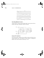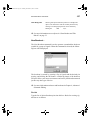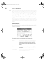
1
LW Reference.bk Page 1 Monday, December 15, 2003 5:59 PM 1 LogicWorks 5 INTERACTIVE CIRCUIT DESIGN SOFTWARE REFERENCE MANUAL Capilano Computing Systems Ltd. North Vancouver, Canada LW Reference.bk Page 2 Monday, December 15, 2003 5:59 PM 2 Copyright 2003 Chapter by Capilano — Computing Systems Ltd. All rights reserved. LogicWorks is a trademark of Capilano Computing Systems Ltd. LW Reference.bk Page iii Monday, December 15, 2003 5:59 PM Contents 1 Introduction Support on the Internet 1 LogicWorks 5 Description 1 General Features 1 Schematic Drawing Features 2 Simulation Features 3 1 New Features in Version 4 4 Limitations in This Version 4 Where to Start 4 Copyright and Trademarks 5 2 Schematic Editing Design Structure 7 What is a Design? 7 What is a Circuit? 8 Types of Objects in a Circuit 8 Design Operations 9 Creating a New Circuit 10 Closing a Design 10 Disposing of a Design File 10 Navigating Around a Schematic 10 7 The Clipboard 11 Using Clipboard Data From Other Programs 12 Using Clipboard Data From LogicWorks 12 Selecting Circuit Objects 13 Selecting a Device 13 Selecting a Text Object 13 Selecting a Picture Object 13 Selecting a Signal 13 Selecting a Pin 14 Selecting Groups of Objects 14 iii LW Reference.bk Page iv Monday, December 15, 2003 5:59 PM iv Changing Search Order 15 Deselecting a Selected Object 15 Classes of Devices 15 Device Libraries 16 How Device Symbols are Created and Stored 16 Placing and Editing Devices 17 Selecting a Device From a Library 17 Duplicating an Existing Device 17 Deleting a Device 18 Moving a Device 18 Entering Device Attributes 18 Drawing Signals 19 Interconnecting Signals 19 Signal Line Editing 20 Name and Pin Number Operations 22 Naming Signals and Busses 22 Device Names 24 Adding an Invisible Name 26 Making an Invisible Name Visible 26 Auto-Naming Features 26 Removing a Name 28 Editing a Name 28 Moving a Name 28 Setting and Editing Pin Numbers 28 Text Objects 30 Creating a Text Notation 31 Editing Free Text 31 Text Style and Display Options 31 Sheet Borders and Title Blocks 32 Creating a Sheet Border 32 Pasting Graphics onto the Diagram 33 Setting Graphic Item Properties 33 3 Advanced Schematic Editing Bussing 35 Properties of Busses 35 Properties of Breakouts 36 Bus Operations 38 Bus Pins 41 Power and Ground Connections 42 Using Signal Connector Devices 42 Creating Signal Connectors in a Library 42 Connectors and Discretes 43 Handling Connectors 43 35 Handling Discrete Components 44 Using Attributes 45 Default Values 45 Attribute Limitations 45 Predefined Attribute Fields 46 Editing Attribute Data (General) 47 Editing Device Attribute Data 48 Displaying an Attribute on the Schematic 48 Rotating Attribute Text 48 Setting Attribute Text Style 49 LW Reference.bk Page v Monday, December 15, 2003 5:59 PM v Using Subcircuits 49 A Simple Subcircuit Example 50 Subcircuit Primitive Type 52 Port Interface 52 Creating a Subcircuit—Top–Down 55 Creating a Subcircuit—Bottom–Up 57 4 Simulation General Information on Simulation 59 Type of Simulation 59 Simulation Memory Usage 60 Time Units 60 Signal Simulation Characteristics 61 Signal States 61 Stuck–At Levels 64 Resolution of Multiple Device Outputs 65 Resistive vs. Forcing Drive 66 Signal Probe Tool 66 Busses 68 Bus Pins 68 Device Simulation Characteristics 69 Device and Pin Delay 69 59 Device Storage State 71 Input Signal Values 72 Device Pin Types 72 Device Pin Inversion 72 Simulation Clearing and Initialization 74 The Clear Simulation Operation 74 The Clear Unknowns Operation 74 Setting Initial Values 75 Schematic Simulation Issues 76 Working With Subcircuit Devices 76 Power and Ground Connectors 80 Special Signal Names 0 and 1 81 Simulation Models 81 Primitive Devices on the Schematic 82 Simulation Pseudo–Devices 82 5 The Timing and Simulator Tools The Timing Window 83 Displaying Signals in the Timing Window 84 Adding a Signal Trace 84 Removing a Signal Trace 84 Repositioning Traces 85 83 LW Reference.bk Page vi Monday, December 15, 2003 5:59 PM vi Timing Display Groups 85 The Simulator Toolbar 87 Displaying and Hiding the Simulator Toolbar 87 Simulator Toolbar Time Display 87 Simulator Toolbar Controls 88 Timing Window Editing 90 Selecting Data for Copy/Paste Operations 90 Summary of Timing Edit Commands 93 6 Primitive Devices Schematic and Pseudo–Device Primitive Types 96 Simulation Primitive Types 97 Pin Inversion 100 Gates and Buffers 100 Gate Definition 101 Gate Pin Order 101 Pin Inversions 102 Transmission Gate 103 Three–State Buffer 104 Resistor 105 Logic Devices 106 Multiplexer 106 Decoder 108 Adder/Incrementer 109 Subtractor/Decrementer 110 D Flip–Flop 110 D Latch 111 D Flip–Flop with Enable 111 JK Flip–Flop 112 Register 112 Counter 113 Shift Register 116 Clock 116 95 One Shot 118 I/O Simulation Pseudo–Devices 118 Binary Switch 118 SPST Switch 119 SPDT Switch 119 SPDT Pushbutton 119 Binary Probe 119 Hex Keyboard 120 Hex Display 120 LW Reference.bk Page vii Monday, December 15, 2003 5:59 PM vii 7 RAMs and Programmable Devices The RAM, PROM and PLA Primitive Types 121 RAM Device Characteristics 122 PROM Device Characteristics 123 PLA Device Characteristics 124 Complex Programmable Logic Devices 124 Using the PROM/RAM/PLA Wizard 125 Creating a RAM Device 125 121 Creating a PROM Device from a Data File 127 Creating a PROM Device with Manual Data Entry 128 Creating a PLA from a Data File 130 Creating a PLA Device with Manual Data Entry 132 Editing RAM, PROM, and PLA Devices 133 8 Device Symbol Editing Working With Symbol Libraries 135 Editing Device Symbols 142 Creating a New Part from Scratch— Basic Procedure 143 Editing an Existing Part in a Library 147 Saving an Edited Part Back to its Original Library 148 Saving the Part Under a New Name 148 Zooming the Symbol Editor Window 149 Adding Sequential Pin Names 149 Setting Part and Pin Attributes 152 Editing Symbol Graphics 154 Using the Drawing Tools 154 135 Reordering Graphical Objects Front-ToBack 156 Grouping Graphical Objects 156 Aligning Graphical Objects 156 Rotating and Flipping Graphical Objects 156 Setting Grids 157 Placing Pins on a Symbol 158 Showing, Hiding, Editing or Moving a Pin’s Name 160 Setting the Default Pin Name Prefix 161 Placing a Bus Pin 161 LW Reference.bk Page viii Monday, December 15, 2003 5:59 PM viii Saving Frequently-Used Graphics and Pins 162 Displaying the Symbol Gallery Window 162 Hiding the Symbol Gallery Window 163 Using Elements from the Symbol Gallery 163 Adding Elements to the Symbol Gallery 163 Specifying a Symbol Gallery File 164 Creating Special-Purpose Symbols 176 Assigning a Primitive Type 176 9 Menu Reference LogicWorks File Menu Commands 177 New 177 Open 178 Close 179 Save/Save As... 179 Revert 179 Print... 179 Print Setup 180 Exit 180 Edit Menu Commands 180 Undo 180 Redo 181 Using the Clipboard 181 Delete 184 Duplicate 184 Point 184 Text 185 Zap 186 Draw Signal 186 Draw Bus 187 Select All 187 177 View Menu Commands 187 Screen Scaling Commands 187 Normal Size 188 Reduce To Fit 188 Zoom In 188 Zoom Out 188 Magnify 188 Schematic Menu Commands 189 Go To Selection 189 Orientation... 189 Get Info... 190 Picture Info Box 196 New Breakout... 197 Push Into 199 Pop Up 199 Attach Subcircuit... 200 Detach Subcircuit 201 Discard Subcircuit 201 Design Preferences... 202 Center in Page 204 Simulation Menu Commands 204 Speed 204 Single Step 205 LW Reference.bk Page ix Monday, December 15, 2003 5:59 PM ix Simulation Params... 205 Add to Timing 209 Add Automatically 209 Add as Group 209 Import Timing (Text)... 210 Export Timing (Text)... 211 Print Timing... 211 Print Setup... 211 LogicWorks Help Menu 211 About LogicWorks... 211 LogicWorks Online 212 Device Pop-Up Menu 212 Device Info... 212 Attributes... 212 Name... 212 Rotate and Flip Commands 213 Cut 213 Copy 213 Duplicate 213 Delete 213 Signal Pop-Up Menu 214 Signal Info... 214 Attributes... 214 Name... 214 Cut 215 Copy 215 Duplicate 215 Delete 215 Pin Pop-Up Menu 216 Pin Info... 216 Attributes... 217 Bus Pin Info... 217 Circuit Pop-Up Menu 219 Normal Size / Reduce To Fit / Zoom In/ Zoom Out 219 Circuit Info... 220 Attribute Pop-Up Menu 220 Edit... 220 Justification... 220 Hide 221 Delete 221 Duplicate 221 Rotate Left / Rotate Right 221 Show Field Name 221 Library Manager Submenu 222 Edit Part 222 New Lib... 222 Open Lib... 222 Close Lib... 223 Lib Maintenance... 223 Device Editor Objects Menu Commands 225 Bring To Front / Send To Back 225 Group / Ungroup 225 Align 225 Move to Grid 225 Device Editor Options Menu Commands 226 Grids... 226 Add Pins 227 Autocreate Symbol 227 Subcircuit / Part Type 227 Part Attributes 227 Text Font... 228 Text Rotation 228 Timing Trace Pop-up Menu Commands 228 Undo 228 Copy 228 Paste 229 Select All 229 Find... 229 Display On 230 LW Reference.bk Page x Monday, December 15, 2003 5:59 PM x Display Off 230 Normal Size 230 Enlarge 230 Reduce 230 Timing Options... 230 Timing Label Popup Menu Commands 232 Get Info... 232 Go To Schematic 232 Remove 232 Group 232 Ungroup 232 Appendix A— Primitive Device Pin Summary 233 Schematic Symbol Primitive Types 233 Pseudo-Device Primitive Types 234 Simulation Primitive Types 235 Appendix B— Device Pin Types What Pin Types Are Used For 239 Pin Types Table 240 Device Pin Type and Simulator Efficiency 241 Bidirectional Pins 241 239 Output Pins 242 Input Pins 242 Appendix C— Initialization File Format (for Windows) [System] Section 243 Modules Directory 243 Default System Font 244 Printer Scale Lines 244 243 LW Reference.bk Page xi Monday, December 15, 2003 5:59 PM xi [System Font Translations] Section 245 [Drawing] Section 245 Initial Directory Settings 245 Font Settings 245 Color Settings 246 Default Design 246 Disabling Untitled Design at Startup 247 Solid Grid Lines 247 Zoom Factors 247 Pin Spacing 248 Breakout Parameters 248 Disabling “Loose End” Markers on Signal Lines 248 Undo Levels 249 Appendix D— Timing Text Data Format General Description of Format 256 Header Format 256 Single Signal Items 257 Grouped Items 257 Data Line Format 257 Timing Text Example 258 Fine-Tuning Pin Number Text Display 249 [Libraries] Section 249 Specifying Libraries to Open at Startup 249 Section [DevEditor] 250 Default Font 250 Grid Settings 251 Default Pin Name 251 Symbol Gallery Location 251 [Timing] Section 252 [DevEditor] Section 253 Default Font 253 Grid Settings 253 255 LW Reference.bk Page xii Monday, December 15, 2003 5:59 PM xii LW Reference.bk Page 1 Monday, December 15, 2003 5:59 PM 1 Introduction Welcome to the world of electronics design using LogicWorks! The purpose of this tutorial/manual is to get you acquainted as quickly as possible with all the powerful editing and simulation features of the program. Support on the Internet Capilano Computing operates an active World Wide Web site for LogicWorks users at www.logicworks5.com. Visit the site for program updates, installation assistance, technical support, user-contributed libraries, program add-ons and up-to-date information on using LogicWorks. LogicWorks 5 Description General Features Compatible with all computers running Windows 98 or newer. Fully interactive operation. Any change to a circuit, input, or device parameter immediately affects displayed circuit activity. The timing diagram is updated and scrolls continuously as the simulation progresses. LogicWorks is upward-compatible to the full DesignWorks© professional circuit-design system. All files created in LogicWorks can 1 LW Reference.bk Page 2 Monday, December 15, 2003 5:59 PM 2 Chapter 1—Introduction be read by DesignWorks. The reverse, however, is not true due to the additional structural features in DesignWorks. Schematic Drawing Features The DevEditor module (included with LogicWorks) allows you to create libraries of custom device symbols using familiar drawing tools. Any circuit can be attached to a symbol as a subcircuit to create a simulation model. The subcircuit can be opened at any time to view or modify internal operation. A circuit schematic can be up to a total of 5 feet by 5 feet. Any number of circuit windows can be open simultaneously, allowing easy copying of partial or complete diagrams from one file to another. Each circuit is displayed in a separate window with independent control of scroll and zoom. Commands and drawing modes can be selected using menu items, keyboard equivalents, or a tool palette that is always visible in each window. Any group of objects on the drawing can be repositioned with a simple click-drag mouse action. Signal lines are rerouted interactively to maintain right-angle connections. Multiple signal-line routing methods allow most pin-to-pin connections to be made with only two mouse clicks. Signal names are global across a schematic. Like-named signals are thus logically connected for simulation and netlisting purposes. Free text created in other programs can be pasted onto a circuit schematic. Similarly, complete or partial circuit diagrams can be pasted into word-processing or drafting documents. Objects can be drawn in user-selectable colors on machines equipped with a color display. Circuit and timing diagrams can be printed on any laser, inkjet, or dotmatrix printer that is supported by a Windows device driver. LW Reference.bk Page 3 Monday, December 15, 2003 5:59 PM LogicWorks 5 Description 3 Simulation Features Full digital simulation capability. Circuit output may be displayed in the form of timing diagrams or on simulated output devices. Uses thirteen signal states, including forcing and resistive drive levels to correctly simulate circuits with design errors such as unconnected inputs or conflicting outputs. Device delay time for individual primitive components may be set to any integer from 0 to 32,767. The timing display has adjustable time-per-division and reference-line placement. Common SSI and some MSI devices are implemented as primitives with hard-coded simulation functions. These can be used to create higher-level device functions. These primitive devices are “scalable,” so you can create a 28-input AND gate or a 13-bit counter, for example, as a single primitive device. Test and control devices, such as switches and displays, are active right on the schematic diagram, allowing circuit operation to be directly controlled and observed. A Clock generator device produces signals with variable period and duty cycle. Any number of clock generators can exist in one circuit. Programmable Logic Arrays can be created with up to 256 inputs and 256 outputs with user-specified binary logic. When used with ABEL© Student Edition Logic Compiler, PLA logic can be specified using Boolean equations and state-transition logic. Programmable ReadOnly Memories with up to 16 inputs and 128 outputs can also be simulated. A simulation control palette allows the circuit to be single-stepped or run at various speeds. RAM devices of any configuration from 1 × 1 to 1Meg × 64 can be created and simulated (based on available memory). Device options include 0 or 1 OE inputs, 0 to 3 CE inputs, separate- or combined-data I/O pins, and three-state or normal outputs. LW Reference.bk Page 4 Monday, December 15, 2003 5:59 PM 4 Chapter 1—Introduction New Features in Version 4 Completely new user interface with extensive new on-screen tools and dockable windows. PLA/PROM/RAM Wizard guides you through the process of creating simulation models for these device types. Add borders and title block to circuit diagrams to create finished, professional-looking printed documentation. Paste graphics from any outside drawing program onto the LogicWorks schematic. Limitations in This Version The absolute maximum number of devices in a master circuit or subcircuit is 32,767. A typical maximum number of devices without severe performance degradation is 500–2,000, depending on processor model. The maximum length of a pin number is 4 characters. The maximum length of a device, pin, or signal name is 16 characters. The maximum length of a device-type name is 32 characters. The maximum number of pins on a device is 800. The entire circuit must fit into available memory. Where to Start We suggest you ease yourself into the world of schematic editing and simulation with LogicWorks by taking the following steps: 1. 2. 3. Install the package using the procedures outlined in Chapter 2, Getting Started, and read any “ReadMe” files supplied on the disk with the package. If you are using LogicWorks for the first time, work first through Chapter 4, Tutorial. It provides step-by-step instructions for basic schematic editing. Refer to Chapter 5, Schematic Editing, for background on basic editing techniques. LW Reference.bk Page 5 Monday, December 15, 2003 5:59 PM Copyright and Trademarks 5 Copyright and Trademarks The LogicWorks software and manual are copyrighted products. The software license you have purchased entitles you to use the software on a single machine, with copies being made only for backup purposes. Any unauthorized copying of the program or documentation is subject to prosecution. The names LogicWorks and DesignWorks are trademarks of Capilano Computing Systems Ltd. A number of other product trademarks are referred to in this manual. Full credit for these is given in the acknowledgments. LW Reference.bk Page 6 Monday, December 15, 2003 5:59 PM 6 Chapter 1—Introduction LW Reference.bk Page 7 Monday, December 15, 2003 5:59 PM 2 Schematic Editing This chapter describes the elements of a LogicWorks circuit design and the procedures you can use to create one. Design Structure What is a Design? In LogicWorks, the term “design” refers to a complete, independent set of circuitry, including all the information needed to display, edit, and simulate it. The following rules outline how a design is stored: A single design is stored in a single file and no logical connections are made between designs. All information required to display and edit a design is stored in the design file. A design never makes reference to external library files. When a symbol is used from a library, all information needed is read from the library and stored with the design. Changing the original library definition will not automatically update the design. A design has a top-level circuit, referred to as the master circuit. This circuit may contain any number of devices which themselves can contain circuits, called subcircuits. Subcircuits can be nested to any desired depth, limited only by available memory. Many LogicWorks operations, such as text report generation, apply only to the master circuit. When a design file is opened, the entire contents of the design are read into memory. This means that design sizes are limited by the available 7 LW Reference.bk Page 8 Monday, December 15, 2003 5:59 PM 8 Chapter 2—Schematic Editing memory in your computer and increasing the memory allocated to the program will increase the size of the designs you can work with. A number of user-selectable parameters are stored with the design and affect the entire design when changed. These include: Attribute and pin number text style settings Display options, such as crosshairs and printed page breaks Printer page setup. What is a Circuit? In LogicWorks, the term “circuit” refers to a single circuit page, as displayed in a single window. Each master circuit or subcircuit consists of one page. Each circuit is viewed in a separate circuit window, and any number of circuits or subcircuits can be displayed on the screen simultaneously. A circuit page is drawn on the screen as if it were a single piece of paper, although it may have to be broken up into a number of individual sheets of paper for printing or plotting. If the circuit is a subcircuit, then logical connections to the parent device symbol are made using the Port Connector device. Port connectors in the subcircuit are matched by name with pins on the parent device. See more information on subcircuits and port connectors in Chapter 6, Advanced Schematic Editing. Types of Objects in a Circuit A LogicWorks circuit is made up of three types of entities: devices, signals, and text objects. A device is an object having a symbol, signal connection points called “pins,” and optional attributes, internal circuit, and simulation information. A device in LogicWorks can correspond to a physical device in a circuit, or it can be a pseudo-device, such as a Ground LW Reference.bk Page 9 Monday, December 15, 2003 5:59 PM Design Operations 9 connector or bus breakout which is used for schematic notation purposes. A pin is a connection point on a device. A pin is not an independent entity, since it only exists as part of a device and cannot be created or deleted separately. However, pins can have attributes, pin numbers, and other parameters that may be different from pin to pin on the same device. The Get Info command can be used on a selected pin to view and set pin parameters. A bus pin is a special type of pin that represents an arbitrary number of internal pins. The internal pins are not visible on the schematic but can still have the same logical properties as other pins. A signal is a conductive path between device pins. Signal connections can be made visually by drawing lines between device pins, or logically by name or bus connection. A text object is used to place a title block or other notation on the diagram. Text can be typed and edited directly within LogicWorks, or can be created externally and pasted onto the diagram from the Clipboard. Text objects are not associated with any other object and are not accessible through net or component lists. The attribute facilities should be used to associate text with specific devices or signals. A picture object is used to place a border, logo, or mechanical drawing on the diagram. Picture objects can be created externally and pasted onto the diagram from the Clipboard or created using the device symbol editor. Once placed, a picture object becomes a single element that can be moved, duplicated, and deleted, but it cannot be edited within LogicWorks. Design Operations This section describes how to work with LogicWorks circuit designs. LW Reference.bk Page 10 Monday, December 15, 2003 5:59 PM 10 Chapter 2—Schematic Editing Creating a New Circuit To create a new design, click on the New Document button ( ) in the toolbar, or select the New item in the File menu, then select Circuit from the list of document types. The new design will consist of an empty master circuit that will appear in a circuit window as Circuit1.CCT, Circuit2.CCT, and so on. This command does not create a disk file. The design exists only in memory until you save it using the Save As command. Your circuit diagram is created by first placing one or more devices in the circuit window (as described below), and then interconnecting the device pins with signal connections. Closing a Design A design is closed when its master circuit window is closed. At the top left corner of the master circuit’s window, click on the X icon or select the Close command from the File menu. In either case, you will be prompted to save the design before closing if any changes have been made. Disposing of a Design File LogicWorks has no built-in command to dispose of a design file. All information about a design is stored in a single file. You may, however, simply delete this file via the Windows Explorer. Navigating Around a Schematic In addition to the standard scroll bars and Reduce/Enlarge menu items, LogicWorks has a number of convenient features for moving around a diagram. LW Reference.bk Page 11 Monday, December 15, 2003 5:59 PM The Clipboard 11 Auto-Scrolling Whenever the mouse button is depressed and moves close to the edge of a Schematic window, the window automatically scrolls to expose more area on that side. Zoom (Magnifying Glass) Tool The item in the Tool Palette is a powerful tool for moving around in a schematic diagram. Once you have activated this tool, it can be used to zoom in and out, and to control the exact area displayed on the screen. Clicking and releasing the mouse button on a point on the diagram will zoom in to that point by one magnification step. Clicking and dragging the mouse down and to the right zooms in on the selected area. The point at which you press the mouse button will become the top left corner of the new viewing area. The point at which you release the button will become approximately the lower right corner of the displayed area. The circuit position and scaling will be adjusted to display the indicated area. Clicking and dragging the mouse upward and to the left zooms out to view more of the schematic in the window. The degree of change in the scale factor is determined by how far the mouse is moved. Moving a small distance zooms out by one step (equivalent to using the Reduce command). Moving most of the way across the window is equivalent to choosing the Reduce to Fit command. The Clipboard The standard Clipboard commands, Cut, Copy, and Paste, can be used to move or copy circuit fragments, graphical, and text information within a single circuit window, between windows, or between LogicWorks and other programs (e.g., word-processing or graphics packages). LW Reference.bk Page 12 Monday, December 15, 2003 5:59 PM 12 Chapter 2—Schematic Editing Using Clipboard Data From Other Programs When you start up LogicWorks, the Clipboard may contain text or graphical information cut or copied from a document in another program. LogicWorks allows you to make use of this information as follows: Text information from a word processor or text editor can be pasted into a text block. Picture information from other applications can be pasted onto a LogicWorks circuit diagram. See more information in the Edit menu section of Chapter 12, Menu Reference. Using Clipboard Data From LogicWorks When a Cut or Copy is performed, two types of data are placed on the Clipboard: A bitmap picture (Windows BMP format) of the selected items. This could be pasted into a graphics document using most drawing programs. The LogicWorks circuit info for the selected items. This data is in a format that only LogicWorks can understand, and is discarded when you Quit. This means that you cannot transfer circuit information between LogicWorks sessions. The Cut and Copy commands work on the currently selected group of objects and will be disabled if nothing is selected. See the section below on “Selecting Circuit Objects.” When items are copied onto the Clipboard, their names are copied with them, which may result in duplicate names. If duplicate signal names are pasted back into the circuit from which they were copied, then logical connections will be made between the likenamed segments. See more information in the Edit menu section of Chapter 12, Menu Reference. LW Reference.bk Page 13 Monday, December 15, 2003 5:59 PM Selecting Circuit Objects 13 Selecting Circuit Objects Many LogicWorks commands, such as Get Info, Cut, Copy, etc., operate on the currently selected objects. To select circuit objects, the cursor must be in the normal Point ( ) mode. Selecting a Device A single device is selected by clicking the mouse button with the pointer positioned anywhere inside the device symbol, or in any displayed attribute value associated with the symbol. Simulated input devices, such as switches and keyboards, can only be selected by holding the key while clicking. This is necessary because a normal click is used to change the state of these devices. Selecting a Text Object A single text item is selected by clicking the mouse button with the pointer positioned anywhere inside the item. Selecting a Picture Object A single picture item is selected by clicking the mouse button with the pointer positioned anywhere inside the item. Selecting a Signal A single signal is selected by clicking anywhere along the signal line. This selects only the part of the signal directly attached to the clicked line. Double-clicking the signal selects all parts of the signal, including logical connections by name or bus. LW Reference.bk Page 14 Monday, December 15, 2003 5:59 PM 14 Chapter 2—Schematic Editing Selecting a Pin A pin is selected by clicking on the pin line close to the device. NOTE: Since an unconnected device pin is both a pin and a signal, you determine whether you get the pin or signal pop-up menu as follows: Right-clicking on the pin in the last 1/4 of the pin length away from the device will display the signal menu. Selecting the Signal In either version, clicking on the pin close to the device symbol will display the pin menu. Selecting the Pin Selecting Groups of Objects Several methods are available for selecting multiple objects: Any group of adjacent items can be selected by activating the Point tool and clicking and dragging across the group. A flickering rectangle LW Reference.bk Page 15 Monday, December 15, 2003 5:59 PM Classes of Devices 15 will follow the mouse movement. Any object that intersects this rectangle when the button is released will be selected. A group of interconnected devices and signals is selected by doubleclicking on any device in the group while holding down the key. If a circuit is completely interconnected, this will select the entire circuit. The Select All command in the Edit menu selects all items in the current circuit design. The key can be used in combination with any of the above methods to select multiple items. When the key is held, the previously selected items remain selected when a new item is clicked on. Thus you can add to the selected group until the desired collection of items is selected. Changing Search Order Holding down the key while clicking the pointer causes object types to be searched in the opposite order from normal. This can be used, for example, to select a signal name that has accidentally moved under a device. Deselecting a Selected Object All currently selected objects are deselected by clicking in an empty area of the Schematic window. A single item can be deselected by holding the key while clicking on it. Classes of Devices For the purposes of this section, devices in LogicWorks can be divided into four groups: Symbol-only devices: These are symbols which are used to represent physical devices on a schematic, but which have no simulation LW Reference.bk Page 16 Monday, December 15, 2003 5:59 PM 16 Chapter 2—Schematic Editing function. For example, the analog components provided in the discrete.clf library fall into this category. Subcircuit devices: These are symbols which have a simulation function defined by an internal circuit. The 7400 devices provided with LogicWorks fall into this category. The internal circuit for this kind of symbol can be viewed by double-clicking on the symbol. Pseudo-devices: These are the symbols used for bus breakouts, power and ground symbols, and so on. They do not represent an actual physical device in a circuit, but they have specific meanings on the schematic diagram. Simulation primitives: These are device symbols which have a builtin simulation function when used with the LogicWorks simulator. See a description of LogicWorks primitive types in Chapter 9, Primitive Devices. Device Libraries The symbols and related parameters for LogicWorks devices are stored in data files called device libraries. Libraries can be opened and closed by displaying the Parts Palette’s pop-up menu and using the Open and Close commands, or by using entries in the initialization file. For each device symbol in a library, the following data is stored: General information on the type, such as number of pins, number of inputs, number of outputs, type name, default delay, default attributes, position, orientation and type of each pin, and so on. A picture representing the symbol for this type. An optional internal circuit definition. How Device Symbols are Created and Stored Libraries are created and modified using the DevEditor tool, which is described elsewhere in this manual. LW Reference.bk Page 17 Monday, December 15, 2003 5:59 PM Placing and Editing Devices 17 See Chapter 11, Device Symbol Editing, for more information. Placing and Editing Devices Selecting a Device From a Library To select a device from a library for placement in the schematic: If necessary, use the scroll bar to scroll the library’s parts list until the desired part name is in view. Double-click on the part name in the list. Move the cursor to the current Schematic window. The cursor will be replaced by an image of the selected device. While moving this flickering image around, you can use the arrow keys on the keyboard, or the orientation tools on the Tool Palette, to rotate the symbol. Clicking anywhere in the circuit diagram will make a permanent copy of the flickering device at that point. NOTE: Holding down the key while clicking will inhibit checking for pin connections. This allows you to select the device again and drag it to a new position without affecting any existing connections. Duplicating an Existing Device To duplicate an existing device on the schematic, either: Select a similar device anywhere on the current circuit and use the Duplicate command (either in the Edit menu or in the device pop-up menu); or: Select a similar device in any other open circuit window and use the Copy command. Return to the destination circuit window and select the Paste command. LW Reference.bk Page 18 Monday, December 15, 2003 5:59 PM 18 Chapter 2—Schematic Editing After either of these operations, the cursor will be replaced by a flickering image of the selected device. This copy can be placed by clicking in the schematic, as discussed earlier. Deleting a Device Devices can be removed by either of two methods: Select the device by clicking on it (holding the key if it is a switch or other input device). Then press the or key on the keyboard, or select the Clear command from the Edit menu. Or: Enter Zap mode, by selecting the Zap command on the Edit menu or clicking on the Zap icon in the Tool Palette. Then click on the device in question. Moving a Device Devices can be moved by clicking and dragging them to the desired new position. If more than one device is selected, all the devices, and all signals connecting between them (whether or not selected), will be moved. Signal lines will be adjusted to maintain right angles at points where moving signal lines intersect with non-moving ones. Entering Device Attributes To enter device attributes, either: Display the device’s pop-up menu (right-click on the device). Then select the Attributes command, or do the following: Select the device by clicking on it normally. Then choose the Get Info command from the Schematic menu, and click the Attributes button. See more information on entering and using attributes in Chapter 6, Advanced Schematic Editing. LW Reference.bk Page 19 Monday, December 15, 2003 5:59 PM 19 Drawing Signals Drawing Signals Signal lines are drawn in either Point ( mode. ) mode or Signal Drawing ( ) Interconnecting Signals If you draw a signal line so that the end of the line makes contact with a second signal line, then those two signals will be interconnected. Also, if you place a new device so that one of its pins touches an existing signal line, that pin will be connected to the signal. If both of the signals being connected were named, then you will be prompted to choose the name of the resulting signal. Whenever three or more line segments belonging to the same signal meet at a given point, an intersection dot will be placed at that point automatically. NOTE: For efficiency, signals are only checked for connections at their endpoints and only signals actively being edited are checked. It is possible to create overlapping lines that do not connect by unusual combinations of editing operations. This situation is usually visually apparent at the time the editing is done, since the intersection dot will be missing and the entire signal will not highlight when clicked on. See more information on connection-checking under the Paste command in Chapter 12, Menu Reference. Connecting Signals by Name See the section below on Name and Pin Number Operations for details on how signals are connected by name. LW Reference.bk Page 20 Monday, December 15, 2003 5:59 PM 20 Chapter 2—Schematic Editing Signal Line Editing Drawing from an Existing Line or a Device Pin A line can be extended from the end of an existing line or device pin using the arrow ( ) cursor. Click and hold on the end of the pin and drag away from the pin. A pair of right-angle lines will follow the cursor away from the pin as long as the mouse button is pressed. Releasing the mouse button makes these lines permanent. If the end of the line (i.e., the point where the mouse button was released) touches another signal line, a connection will be made at that point. Alternate line-routing methods can be activated by pressing the keys, as follows: No keys pressed key pressed key pressed and keys pressed The key inverts the order of line drawing, and the switches to three line segments with a center break. The strains the movement to a single vertical or horizontal line. NOTE: and key key con- Holding the key while clicking will inhibit checking for pin connections. This allows you to select the signal again and drag it to a new position without affecting any existing connections. Creating an Unconnected Signal Line The Draw Sig ( ) tool can be used to create an unattached signal line, or to extend an existing signal. Simply click anywhere in the schematic and drag in the desired direction. Unlike the Point mode drawing method, LW Reference.bk Page 21 Monday, December 15, 2003 5:59 PM 21 Drawing Signals above, the mouse button does not have to be held down while creating signals in this mode. Double-clicking terminates the signal line. Editing a Signal Line The following features are available to edit signal lines: Zap mode (entered by selecting the Zap command in the Edit menu or the Zap item in the Tool Palette) allows you to remove any single line segment from a signal connection. Zapping on a signal line removes only the line segment to which you are pointing—up to the nearest intersection, device pin, or segment join point. Before Zap After Zap Selecting a signal line (by clicking anywhere along its length), then hitting the key or selecting the Clear command from the Edit menu, removes an entire signal trace. Drawing backwards along the length of an existing line causes the line to be shortened to end at the point where you let the button go. Clicking and dragging the middle of a signal line segment allows you to reposition the line. Vertical lines can be moved horizontally and vice versa. Checking Signal Interconnection Double-clicking anywhere along a signal line will cause that signal segment and all logically connected segments to be selected. LW Reference.bk Page 22 Monday, December 15, 2003 5:59 PM 22 Chapter 2—Schematic Editing Name and Pin Number Operations Names may contain any letters, numbers, or special characters that you can type on the keyboard, but are restricted in length to 15 characters. The name associated with an object can be placed anywhere on the diagram, and will be automatically removed if the object is removed. Pin numbers may contain at most 4 characters. Naming Signals and Busses What Signal Names are Used For The signal name is referenced by the following LogicWorks functions: The signal name is used in Report Generator output, such as netlists. Signals can be logically interconnected by name. Signal names are used to identify traces in the Timing window. Adding a Signal Name To name a signal, enter Text mode, either by selecting the Text command in the Edit menu, or by clicking on the text icon in the toolbar: Text Tool Note that once “Text” is selected, the cursor changes to a pencil icon. Press and hold the mouse button with the tip of the pencil positioned anywhere along a signal line except within five screen pixels of the device. As long as you hold down the mouse button, an I-beam cursor will track the mouse movements. The signal-name text will start at the position where you release the button. Type the desired name, and press or click the mouse button anywhere. LW Reference.bk Page 23 Monday, December 15, 2003 5:59 PM 23 Name and Pin Number Operations Position the pencil cursor anywhere along the signal line. Click and hold the mouse button. The cursor changes to an I-beam. Still holding down the mouse button, position the cursor where you want the name to start. Release the mouse button. A blinking insertion marker appears. SYNC1| Type the desired name, up to 15 characters. SYNC1 Press the Enter key, or click the mouse button once, to make the name permanent. Multiple Naming of Signals A signal name can appear in up to 100 positions along the length of the same signal line. To add a new position, simply use the normal naming procedure given in the section on signal naming, such as: Select Text mode. Click and drag anywhere along the signal line. Release the mouse button. A new copy of the signal’s name will appear at this point, followed by a flashing cursor. To accept the name, simply click the mouse button once or press the key. If you edit any occurrence of a name along a signal segment, all other occurrences will be updated to reflect the new name. Any occurrence of a signal name can be removed using the Zap tool. If you remove the last visible name from a signal segment, then the logical connectivity to other like-named signals is removed. Connecting Signals by Name Signal names can be used to make logical connections between lines that are not visually connected on the schematic. The following rules apply: Signal names must be visible to be checked for connections, unless a Signal Connector device (such as Ground) is attached. More information on invisible names is given in the following section. LW Reference.bk Page 24 Monday, December 15, 2003 5:59 PM 24 Chapter 2—Schematic Editing Signal names are known throughout a schematic page. Like-named signal lines are thus logically connected for simulation and netlisting purposes. Whenever a signal name is added or changed, the circuit is checked for a change in connectivity. If the name is now the same as another signal, the two signals are merged into one. If this signal segment was previously connected by name to others, and the name is changed, then the logical connection is broken. Whenever a name change causes two signals to be connected, the changed signal will flash on the screen to confirm the connection. Signals which are contained in busses are a special case. Every signal contained in a bus has a name, even if it is not displayed on the diagram. However, the names of bussed signals will not be used to make logical connections unless an explicit name label has been added to the signal line. For example, if you have a bus containing a signal named CLK and a separate signal line also named CLK, there will be no logical connection between these two signals. The name appearing on the bus breakout is part of the breakout symbol and is not considered to be a name label. If an explicit label is added to the bussed CLK signal (using the text cursor) then the two CLKs will be logically connected. The same rules discussed above for signals also apply to busses. Whenever two busses are logically connected, all like-named internal signals also become logically connected. Device Names In this book, we use the term “device name” to refer to the character string that identifies a unique device in the circuit. Typical device names might be U23, C4, IC12A, and so on. This is distinct from the type name or part name that is used to distinguish the type definition that is read from a device library. Typical part names are 74LS138, MC68000L8, SPDT Switch, and so on. Adding a Device Name Enter Text mode either by selecting the Text menu item in the Edit menu, or by clicking on the text icon in the Tool Palette: LW Reference.bk Page 25 Monday, December 15, 2003 5:59 PM Name and Pin Number Operations 25 Once Text mode is selected, the cursor changes to a pencil icon. Press and hold the mouse button with the tip of the pencil positioned inside a device symbol. As long as you hold down the mouse button an I-beam cursor will track the mouse movements. The device-name text will start at the position where you release the button. Type the desired name, and press or click the mouse button anywhere. Position the pencil cursor anywhere inside the device symbol. Click and hold the mouse button. The cursor changes to an Ibeam. Still holding down the mouse button, position the cursor where you want the name to start. Release the mouse button. A blinking insertion marker appears. Type the desired name, up to 15 characters. Press the Enter key, or click the mouse button once, to make the name permanent. Once a name is placed, it can be repositioned by dragging it using the arrow cursor, or removed using the Zap cursor. The device name will be removed automatically if the device is removed. LW Reference.bk Page 26 Monday, December 15, 2003 5:59 PM 26 Chapter 2—Schematic Editing Adding an Invisible Name An invisible name for either a device or signal can be created in one of two ways. Use the right mouse button to select the device or signal, then select the Name command from the pop-up menu. Or: Select the desired device or signal, then select the Get Info command in the Schematic menu ( –I), then click on the Attributes button in this dialog, then select the Name field in the Attributes Dialog. In either case, if the name is already visible on the diagram, changing it here will change all its displayed occurrences. IMPORTANT: When a signal name is invisible, it is not used to establish connections by name to other signal lines. See the rules in the section above, Naming Signals and Busses. Making an Invisible Name Visible An invisible name can be made visible by either of the following methods: Click the Text pointer anywhere on the signal or device. When the mouse button is released, the name will be positioned at that point, as described in the general naming instructions above. Or: Select the Name command in the device or signal pop-up menu, and enable the Visible option. The name will be displayed in a convenient location close to the object. Auto-Naming Features Three features are available to simplify the naming of groups of related signals, devices, and pins. These features are activated by holding down the , , and/or keys, then selecting the signal to be named with the Text cursor. Auto-alignment—If the key is held down while the signal is selected, the text insertion point will be positioned horizontally aligned with the last signal name that was entered. The vertical position is LW Reference.bk Page 27 Monday, December 15, 2003 5:59 PM Name and Pin Number Operations 27 determined by the vertical position of the line that was clicked on. This feature works only with signal or device names, not with pin numbers. Auto name generation—If the key is held down while a signal, device, or pin is selected, a new name is generated automatically for this item. The new name will be the same as the last one entered, except that the numeric part of the name will have been incremented. If the previously-entered name did not have a numeric part, then a “1” digit will be appended to it. If the key is pressed at the same time, the number will be decremented instead of incremented. Sequential Naming The above two features can be used in combination to perform easy naming of sequential signals. The normal symbol standard in LogicWorks is to position the highest numbers at the top, so you can either: Number the topmost line in the group (e.g., D7) using the normal naming technique, described above. Then hold down the , , and keys while clicking on successive lower-numbered lines. Or: Number the bottom-most line in the group (e.g., D0) using the normal naming technique, described above. Then hold down the and keys while clicking on successive higher-numbered lines. Note that when you select each successive line, the new name appears; however, it is necessary to click again (or press ) to make the name permanent. LW Reference.bk Page 28 Monday, December 15, 2003 5:59 PM 28 Chapter 2—Schematic Editing Removing a Name A device or signal name can be removed by using the Zap pointer, as described in the section on Deleting a Device, above. If the signal has been named in multiple locations, then Zap removes the name only at the location zapped. Editing a Name The name can be changed by simply clicking the Text pointer on the signal name and editing it using the keyboard. Alternatively, a name can be edited by choosing the Name command in the pop-up menu for the device or signal. Changing the name in the resulting dialog—or at any single location on the diagram—will change all visible occurrences of it. Moving a Name A device or signal name can be moved by activating the arrow cursor, clicking and holding the mouse button on the name, and dragging it to the desired new position. Pin numbers cannot be repositioned. Setting and Editing Pin Numbers Pin numbers may contain one to four characters. They are always positioned adjacent to the associated pin. Any characters may be used—not just digits—in order to accommodate alphanumeric pin numbering for pin grid arrays. Uses of Pin Numbers Pin numbers are used only for labeling purposes and have no particular connectivity significance to LogicWorks. Pin numbers are not checked for duplicates or other invalid usage. Pin numbers placed on a diagram will be used in creating a netlist (see Chapter 13, Creating Text Reports), and will appear when the circuit is printed. If a pin is unnumbered, it will appear in a netlist with a “?”—unless the device has three or fewer pins (e.g., discrete components), in which case it will be sequentially numbered. LW Reference.bk Page 29 Monday, December 15, 2003 5:59 PM Name and Pin Number Operations 29 Default Pin Numbers A device symbol may have default pin numbers which will appear when the device is first placed. These pin numbers are not permanent and can be edited or removed by techniques discussed in this section. These default pin numbers are assigned using the DevEditor tool. See Chapter 10, Device Symbol Editing. Editing Pin Numbers On the Schematic In Text mode, if the mouse button is pressed with the tip of the pencil pointer positioned on a signal line within five pixels of a device, a blinking insertion bar will appear immediately where the signal joins the device. You cannot set the text position for pin numbers. Type the desired one- to four-character number, then press or click the mouse button to make the number permanent. Editing Pin Numbers Using Get Info To edit pin numbers using the Get Info dialog box: Display the device’s pop-up menu by right-clicking on the device. From the pop-up menu, choose Device Info. In the Device Info dialog, click on the Pin Info button. This will display the pin information for the first pin. Edit the pin number as desired. Click the Next Pin button to see the next pin in the list. LW Reference.bk Page 30 Monday, December 15, 2003 5:59 PM 30 Chapter 2—Schematic Editing Auto-Numbering Features An auto-numbering feature is provided to simplify numbering of sequential pins. If the key is held down while a pin is clicked with the Text pointer, a new number is generated automatically for this item. The new label will be the same as the last one entered, except that the numeric part of the character string will have been incremented. If the previouslyentered item did not have a numeric part, then a “1” digit will be appended to it. If the key is pressed at the same time, the number will be decremented instead of incremented. Setting Pin Number Text Style The text style for pin numbers is set globally for the entire design. It cannot be set individually for pins. To set pin number text style: Select the Design Preferences command in the Schematic menu. Click on the Pin Text button. Select the desired text font, style and size in the Font dialog. Click OK on the Font dialog, then OK in the Design Preferences dialog. Depending on the size of the design, there may be a short delay at this point while sizes and positions of text items are recalculated. Text Objects Free text objects are used only to enhance the graphical appearance of a schematic diagram. They have no logical significance in the design. IMPORTANT: Free text items are not associated with any particular device or signal on the screen, and should not be used to set a name or attributes for devices or signals. The text in these boxes is not accessible in net or component lists. Use the naming and attribute features to attach text to devices and signals. LW Reference.bk Page 31 Monday, December 15, 2003 5:59 PM Text Objects 31 Creating a Text Notation If you click the text pointer on the diagram away from a device or signal line, a blinking cursor will appear at that point, and you will be able to type any desired text on the diagram. The key or the can be used to enter multiple lines in a single text block. Text entry is terminated by clicking outside of the text entry box. Editing Free Text If you click the text pointer inside an existing text item, the insertion point will be positioned at the click point. You can then use normal text editing techniques to modify the text. Note that text on the Clipboard can be pasted into an existing text box using the –V key equivalent for the Paste function. The Paste menu command will cause the current text entry to be terminated and a new text box to be created. Similarly, the –key equivalents for Cut ( –X) and Copy ( –C) can also be used while editing a text box. Text boxes can be zapped, duplicated, cut, copied, pasted, and dragged just like any other item on the screen. See the descriptions of these commands for more information. Text Style and Display Options To set text display options and text style, select the free text block by clicking on it with the arrow cursor, then select the Get Info command in the Schematic menu. This will display the following dialog: LW Reference.bk Page 32 Monday, December 15, 2003 5:59 PM 32 Chapter 2—Schematic Editing The following table summarizes the options available in this dialog. Rule Between Lines Turning this switch on causes a line to be drawn after each row of characters. Draw Frame Turning this switch on causes a frame to be drawn around the text item on the schematic. Font Specs Clicking this button displays the standard Font dialog. Any changes made in font style affect only the selected item, but they also become the default for future free text blocks. Sheet Borders and Title Blocks LogicWorks provides a number of features to assist in creating the borders and title blocks reqruired for a finished schematic diagram. Creating a Sheet Border Two methods are available for displaying or printing a border on the drawing: The default border mechanism displays and/or prints a border with background grid lines and reference letters and digits at the edges. The border resizes automatically to match the current drawing size. This grid can be turned on and off using the options in the Design Preferences command. To get more control over the appearance of the border, you can create a graphic of the desired size in any Windows application that will export Windows Metafile Format (WMF) data on the clipboard. This image can then be pasted onto the sheet and set to be a background object, using the procedure outlined below. This border will then be a fixed size and will not resize automatically with printer setup and drawing size changes. Any changes will have to be made manually to the original graphic which will then have to be re-pasted into the drawing. LW Reference.bk Page 33 Monday, December 15, 2003 5:59 PM Sheet Borders and Title Blocks 33 Pasting Graphics onto the Diagram Graphics from a number of sources can be pasted directly onto a LogicWorks schematic diagram: Windows Metafile Format (WMF) data is exported by Microsoft Word and many drawing programs, and provides a clean, compact (i.e. a minimal amount of memory is used) and scalable image (i.e. prints cleanly on various types of printers). This is the recommended way of creating border and title block graphics. Bitmap (BMP) images can be created using Windows Paint or many third-party paint programs. NOTE: BMP images are not suitable for large borders since they occupy a large amount of memory space and do not scale well when printing. Graphics can be copied and pasted from the device symbol editor built into LogicWorks. This is a convenient way of creating images that do not require exact measures or sophisticated drawing tools. To do this, select the New command in the FIle menu, select the Device Symbol document type. Draw the desired graphics in the symbol editor, then Select All and Copy them onto the clipboard. Switch back to the schematic sheet and Paste the graphics onto the sheet. You can now close the device symbol editor without saving. NOTE: There is an important difference between graphics created in the Device Editor using the above procedure and device symbols created in the Device Editor and then saved in a library and placed on the sheet from the library. When you copy and paste directly onto the sheet, you are creating only a graphic object, which has no circuit properties and no simulation and will not appear in any component lists. If you create exactly the same graphic, save it as a component in a library and then place it on the diagram, this will have an identical visual appearance, but will be treated within the program as a device. This means it will appear in component lists as a device and it can be given attributes, simulation parameters, etc. Setting Graphic Item Properties To set the properties of a graphical item on the diagram: LW Reference.bk Page 34 Monday, December 15, 2003 5:59 PM 34 Chapter 2—Schematic Editing Click on it once to select it (if the object has been previously set to be a background item, you will have to hold the order to select it. and keys in Select the Get Info command in the Options menu. Select the Draw Frame item to draw a border around the graphic. Select the Make Background item to prevent the item from being selected by a normal mouse click. Note the key sequence given above that is required to select a background object. LW Reference.bk Page 35 Monday, December 15, 2003 5:59 PM 3 Advanced Schematic Editing This chapter provides information on the more advanced schematic editing features of LogicWorks. Bussing The bussing facility allows any combination of named signals to be represented by a single line and any subset of these to be brought out through a “breakout” at any point along the bus line. Properties of Busses A bus is treated by LogicWorks as a signal with special properties. Thus, bus lines can be drawn and modified on the screen using all the same editing features available for signals. Note the following properties of busses: Only bus pins on devices can be connected directly to a bus. All other connections must be made by using a breakout to access the desired internal signals. A breakout is created using the New Breakout command in the Schematic menu. You do not need to specify in advance what signals will be contained in a given bus. Any signals that are present in a breakout or bus pin attached to a bus will become part of that bus and can be brought out through another breakout anywhere along the bus. Any two busses can be joined together, regardless of their internal signals. When two different busses are merged, any signal in either bus becomes available anywhere along the combined bus. 35 LW Reference.bk Page 36 Monday, December 15, 2003 5:59 PM 36 Chapter 3—Advanced Schematic Editing If you select a bus line, then pull down the Schematic menu and select the Get Info command. The displayed info box will show a list of the signals currently contained in the bus. A given signal can be present only in one bus. If you attempt to connect together two signals in different busses, a warning box will be displayed and the connection will be canceled. A bus can be created by drawing the bus lines first, then creating the breakouts to attach, or by creating a breakout and extending the bus line starting at the bus pin. Bus lines are drawn or extended using exactly the same techniques as for signals, except that the Draw Bus command or cursor is used instead of Draw Signal. Properties of Breakouts Signals are attached to a bus via a special type of device symbol called a “breakout.” It is not legal to attach a signal line directly to a bus line. If a signal line touches a bus line, no connection will be made. In LogicWorks, a breakout is treated as a device with certain special properties. This means that it can be placed in any desired orientation, moved, duplicated, etc., using any of the device editing features available. A typical breakout appears as follows: Any breakout can always be attached to any bus. When a breakout is attached that contains signals unknown in that bus, the signals are implicitly added to the bus. For example, suppose we want to add control signals to the above circuit. We could create a breakout containing only the new signals, as follows: LW Reference.bk Page 37 Monday, December 15, 2003 5:59 PM Bussing 37 Once such a breakout has been added to the bus, all signals in all attached breakouts are considered part of that bus. A list of internal signals can be seen by selecting the bus and using the Get Info command: Any combination of the internal signals can now be brought out of the bus at any point, as in the following addition to the above circuit: LW Reference.bk Page 38 Monday, December 15, 2003 5:59 PM 38 Chapter 3—Advanced Schematic Editing Bus Operations Creating a Bus A bus can be created by any one of the following methods: Select the Draw Bus tool ( ) in the Tool Palette. Draw any desired contiguous set of lines on the diagram using the usual signal drawing techniques. This bus will have no internal signals initially. Signals will be added implicitly when it is connected to any breakout or bus pin. Create a breakout symbol using the New Breakout command (see below). The bus pin (backbone) of the breakout can now be extended using the normal pointer ( ) or the Draw Bus cursor. The bus will contain all signals specified in the breakout. Bus Connection Points Extend a line out from an existing bus pin on a device (see below) using the normal pointer or the Draw Bus cursor. The bus will contain all signals specified in the bus pin on the device. Connections between bus internal pins and bus internal signals can be changed using the Bus Pin Info command on the bus pin’s pop–up menu. Adding Signals to a Bus There is no explicit command to add signals to a bus. Signals are added to a bus each time a breakout or device bus pin is connected to the bus. Any signals in the breakout or bus pin are implicitly added to the bus if they don’t exist already. Creating a Breakout To create a breakout, select the New Breakout command in the Schematic menu. If the new breakout is to be similar to an existing one, first select the similar breakout or the bus to which the new breakout is to be connected. LW Reference.bk Page 39 Monday, December 15, 2003 5:59 PM 39 Bussing Then select the New Breakout command. The following dialog box will appear: If a bus or breakout was selected on the circuit diagram, the New Breakout Info dialog will display a list of the signals in that bus or breakout; otherwise, it will be empty. If this list already matches the signals you want in the new breakout, then just click the “OK” button or press on the keyboard. Otherwise, edit the signal list, noting the following options: Blanks or commas can be used to separate individual names in this list; therefore bussed signals cannot have names containing a blank or comma. A range of numbered signals can be specified using the following formats: D0..7 or D0..D7 is equivalent to D0 D1 D2 D3 D4 D5 D6 D7 D15..0 is equivalent to D15 D14 D13 D12 D11 D10 D9 D8 É D0 D15..D00 is equivalent to D15 D14 D13 D12 D11 D10 D09 D08 D07 É D00 LW Reference.bk Page 40 Monday, December 15, 2003 5:59 PM 40 Chapter 3—Advanced Schematic Editing Note that the “..” format implies that bussed signal names cannot contain periods. The signals specified will always appear in the order given in this list from top to bottom in standard orientation. Specifying numbered signals from lowest numbered to highest is a good practice, as in the first example above, since this matches the standard library symbols. There is no fixed limit on the number of signals in a bus, but it is a good practice to divide busses up by function (that is, address, data, control, etc.) for ease of editing. Any combination of randomly–named signals can be included in the list, as in the following examples: D0..15 AS* UDS* LDS* CLK FC0..3 MEMOP BRQ0..2 Once the list has been entered, click on the OK button or press the key. A flickering image of the breakout will now follow your mouse movements and can be placed and connected just like any other type of device. Editing Breakout Pins The signal name notation that appears on a breakout pin is actually a pin attribute. It can therefore be edited by the usual attribute editing mechanisms—that is, either: Select the pin and choose the Get Info command in the Schematic menu, then click the Attributes button; or: Click the text cursor directly in the text on the schematic, as illustrated: b Type the desired new name. LW Reference.bk Page 41 Monday, December 15, 2003 5:59 PM Bussing 41 Press the key. The breakout pin and the attached signal will be renamed as entered. IMPORTANT: The notation on the breakout pin is always the same as the name of the attached signal. Changing the breakout pin renames the attached signal and will detach it from any like–named signals already in the bus. Changing Bus Pin Connections When a bus is connected to a bus pin on a device or subcircuit block, the bus internal pins will by default connect to signals with the same name in the bus. To change these default connections, use the Bus Pin Info command in the pin pop–up menu. See Chapter 12, Menu Reference, for more information. Bus Pins LogicWorks supports user–created bus pins on devices. A bus pin can be defined to have any collection of named internal pins. Note the following properties of bus pins: The bus pin itself does not represent a physical device pin. It is only a graphical place–holder on the schematic representing a group of internal pins. The bus pin itself never appears in a netlist. The internal pins represent physical device pins. Even though they do not appear on the schematic, they can have all the same parameters as normal devices pins, including pin numbers and attributes. These parameters can be accessed using the Bus Pin Info command in the pin pop–up menu. When a device with a bus pin is placed, it has a pre–created bus attached to it by default. This bus will contain one signal for each internal pin, with the initial name of the signal being the same as the name as the pin’s name. A “splicing” box can be displayed using the Bus Pin Info command in the pin pop–up menu. This box allows any internal pin to be connected to any signal in the attached bus. LW Reference.bk Page 42 Monday, December 15, 2003 5:59 PM 42 Chapter 3—Advanced Schematic Editing For more information on creating device symbols with bus pins, see Chapter 10, Device Symbol Editing. Power and Ground Connections LogicWorks uses a type of pseudo–device symbol called a “Signal Connector Device” to maintain connectivity between like–named power and ground symbols that are used on circuit diagrams. As soon as a Ground symbol is placed on the diagram, the attached signal will be named “Ground” (the name will initially be invisible). This will cause it to be connected by name to any other signals that have Ground symbols or are explicitly named “Ground”. Connectivity can be checked at any time by double–clicking on any ground or power line. This will highlight all other like–named lines on the diagram. IMPORTANT: Signal connectors do not cause a logical connection to be made between circuit levels in nested subcircuits. Using Signal Connector Devices Signal Connector Devices are placed on the diagram just like any other LogicWorks device. A set of standard power–supply symbols are included with LogicWorks in the connectors or pseudo devices libraries.. If you connect two different signal connector devices together, you will be prompted to provide a name for the resulting signal. Creating Signal Connectors in a Library Signal Connector devices are special primitive “pseudo–devices” in LogicWorks and can be created using the Set Primitive Type command in the device symbol editor to select the SIGCONN primitive type. LW Reference.bk Page 43 Monday, December 15, 2003 5:59 PM Connectors and Discretes IMPORTANT: 43 The signal attached to a signal connector device is actually named to match the pin name of the signal connector pin specified in device symbol editor, not the type name. In most of the power and ground symbols provided with LogicWorks, these two names are the same. However, it is possible to create a symbol called “Ground” (for example) in a library that actually names the attached signal “GND”. The Ground symbol in the spice.cct library is an example of this—it names the attached signal “0” to match the SPICE ground–naming convention. See Chapter 11, Device Symbol Editing, for more detailed information on this procedure. Connectors and Discretes In LogicWorks, each symbol is considered to be a separate device and each device is normally assumed to be one IC package with a standard pin numbering scheme. Thus connectors and discrete components will require special consideration. Handling Connectors Connectors can be handled in one of two ways: A special symbol can be created for the connector with the appropriate number of pins and pin numbering specified for each pin. This can be done using the device symbol editor to create a device symbol using your own picture. Each connector pin can be created as a separate single–pin device or as a custom symbol. The second option is preferable only if you need to spread the connector pins over different parts of the diagram. In this case, each “device” must be given the name of the connector and the pin number associated with that pin. The report generator will normally merge all devices with the same name into a single component entry. Following is an example of these two methods: LW Reference.bk Page 44 Monday, December 15, 2003 5:59 PM 44 Chapter 3—Advanced Schematic Editing Separate Devices NOTE: Single Device When the single–pin devices are used, every device must carry exactly the same name, although the names can be invisible if desired. Handling Discrete Components Discrete components—such as capacitors, transistors, etc.—can be handled just like any other device, except for the following special considerations. Pin Numbering on Discrete Components Pin numbers are not normally placed on discrete component pins on a diagram. If pin numbers are omitted from a device, LogicWorks will normally put a question mark in the netlist item for that device. Two methods are available to provide pin numbers for netlisting purposes: To provide automatic numbering of discrete devices pins, the Report Generator provides an auto–numbering option. This option causes any device with less than or equal to three pins to be numbered automatically if no pin numbers are present on the diagram. IMPORTANT: This option assumes that the pin number order of the discrete components is not significant. If a specific order is important, do not use this method. Pin numbers can be assigned but left invisible. This is done using the Get Info command for either the pin or the device. LW Reference.bk Page 45 Monday, December 15, 2003 5:59 PM Using Attributes 45 Using Attributes LogicWorks allows arbitrary blocks of text to be associated with any device, signal, or pin in a design, or with the design itself. The blocks of text are called attributes. Attributes have a wide variety of uses, including: Displaying device name, component value, etc. Storing data for use by external systems such as simulators, PCB layout, analysis tools, etc. Default Values A device symbol can incorporate predefined default values for any number of fields. Values can be specified for the device itself, and independently for each pin on the device. When the standard Attributes Dialog is displayed for a device, you will see a button labeled Use Default Value. If this button is grayed out, then there is no default value, or the value shown is already the default. See Chapter 11, Device Symbol Editing, for more information on creating default attribute values. Attribute Limitations Attribute fields have the following specific limitations: Length of field name: 16 characters Length of field data item: 32,000 characters. Number of displayed positions of a single attribute item: 100 Like all other circuit data, the amount of attribute data that can be associated with a design is limited by available memory. LW Reference.bk Page 46 Monday, December 15, 2003 5:59 PM 46 Chapter 3—Advanced Schematic Editing Predefined Attribute Fields The following table describes the fixed list of attribute fields provided in each LogicWorks design. Attribute fields cannot be added or deleted in LogicWorks. Field Name Used In Description CctName Design Design file name. Sets the window title and name of next saved file. Delay.Dev Device Specifies device delay. For most devices, a single decimal integer 0 to 32,767. For Clock and One Shot devices, two integers separated by commas. Should be set using the Parameters command, and not edited manually. Delay.Pin Pin A decimal integer specifying pin delay in the range 0 to 32,767. Should be set using the Simulation Params command and not edited manually. Initial.Pin Pin This field is used to specify the initial state for storage devices when a Reset or Clear Simulation operation is performed. It can contain a single character, either 0, 1, X, or Z. Initial.Sig Sig This field is used to specify the initial state for a signal. It can contain a single character, either 0, 1, X, or Z. Invert.Pin Pin This field is used to specify logical inversion on device pins. Any non–empty value indicates inversion should be done. Name Device, signal The device or signal name. This is the field set using the text tool on the schematic or the Name command in the pop–up menu. Spice Device, Design Holds simulation parameters for SPICE–based simulators. Not used internally. Value Device Component value to appear on the schematic. Not used internally. LW Reference.bk Page 47 Monday, December 15, 2003 5:59 PM Using Attributes 47 Editing Attribute Data (General) The following dialog box is used to enter or edit attribute data: NOTE: The same Attributes Dialog is used to enter data for all object types. This section discusses the general operation of this dialog. The following sections will discuss each object type. Basic Procedure To edit the contents of a field, simply select the field name in the list. The current contents of the field will be displayed in the editable text box. Edit this value using the normal text editing techniques. Select another field or press the Done button if you are finished editing. If the data you typed exceeded the maximum length for the field, or if it contained invalid characters for the field, then you will be asked to correct the data. You can view or edit as many fields as desired while in this dialog. No changes are made to the actual design data until you click the Done button. Clicking Cancel will abandon all changes made while in this dialog. Default Value Clicking the Use Default Value button sets the value for the selected field to the default value stored with the symbol. If this button is inactive (grayed out) then the value is already the default value, or no default value is present. Only devices and pins can have default values. LW Reference.bk Page 48 Monday, December 15, 2003 5:59 PM 48 Chapter 3—Advanced Schematic Editing Editing Device Attribute Data The Attributes Dialog can be entered in one of two ways: Click on the device to select it, then select the Get Info command from the Schematic menu, then click on the Attributes... button. Or: Display the device’s pop–up menu (right–click on the device). Then select the Attributes command from the menu. The standard Attributes Dialog will appear. Select the desired field by clicking on it in the list. The current contents of the selected field will be displayed in the text edit box. This text may be edited using standard editing techniques. Displaying an Attribute on the Schematic To display device, signal, or pin attribute text on a schematic: Display the pop–up menu for the device, signal, or pin to which you want to attach the attribute. (right–click on the device) From the pop–up menu, select the Attributes command to display the Attributes Dialog. Select the desired field by clicking on its name in the field list. Edit the attribute value as desired. Turn on the Visible switch. Click OK. The attribute text will now be displayed in a default position near the device or signal. It can be dragged to any desired location using the Point tool. Rotating Attribute Text To rotate an attribute text item that is already displayed on the schematic: Display the attribute pop–up menu for the text item you want to rotate. (right–click on the text item.) LW Reference.bk Page 49 Monday, December 15, 2003 5:59 PM Using Subcircuits 49 From the pop–up menu, select the Rotate Right or Rotate Left command. Setting Attribute Text Style Attribute text style is set globally for the entire design. There is no way to set text style for an individual item. IMPORTANT: Changing the attribute text style affects all visible attributes throughout the design. LogicWorks may alter text alignment and position to accommodate a new text size. To set the global text style: Choose the Design Preferences command in the Schematic menu. Click on the Attr Text... button. Select the desired font, style and size, then click OK. Click OK in the Design Preferences dialog. Depending on the size of the design, there may be some delay at this point. The program must check all visible attribute items to see if their position and framing is affected by the text change. Using Subcircuits LogicWorks provides the ability to have a device symbol in a schematic actually represent an arbitrary circuit block. This subcircuit can be used to implement a simulation model for a device of arbitrary complexity. Subcircuits can be nested to any desired depth, so devices containing subcircuits can themselves be used as subcircuits for more complex devices. For clarity, a device symbol that represents an internal circuit will be called a “subcircuit device” in the following text. LW Reference.bk Page 50 Monday, December 15, 2003 5:59 PM 50 Chapter 3—Advanced Schematic Editing Following is a short summary of the rules governing subcircuit devices. More information on each of these topics is included in the following sections. The “pins” on the subcircuit device symbol represent connections to specific input–output points on the internal circuit. A “port connector” pseudo–device must be placed in the subcircuit corresponding to each pin on the parent symbol. Port connector symbols are found in the connect.clf library supplied with LogicWorks. A subcircuit device can be opened at any time by double–clicking on the parent symbol. Subcircuits can be “locked” to prevent accidental modification by selecting the Lock Opening Subcircuit option in the Device Info box. Subcircuits cannot be “recursive,” i.e., you cannot use a device symbol inside its own internal circuit. The netlist and bill of materials reports generated by the Report tool in LogicWorks only list components in the top–level circuit in the design. Devices in subcircuits are never listed. A device symbol with an associated subcircuit can be stored in a part library. Each time that symbol is selected from the library, the subcircuit definition will be loaded and attached to the device. When you open a device’s subcircuit, a temporary copy of the subcircuit is made to isolate it from all others of the same type that have been used elsewhere in the design. When you closed the subcircuit, choosing the “update” option will cause all other devices of the same type to be modified. If a given type of subcircuit device has been used more than once in the same design, you can only have one of them open at a time for viewing or editing the subcircuit. Signals in an open subcircuit can be displayed in the Timing window. As soon as the subcircuit is closed, the waveforms for any of its signals that were displayed will be removed. A Simple Subcircuit Example The following diagram is the master circuit, or top level, of our design example: LW Reference.bk Page 51 Monday, December 15, 2003 5:59 PM Using Subcircuits 51 Note that it contains two symbols, both representing subcircuit devices. Both symbols are of the same type, RSFF, and therefore share the same internal circuit definition. The two devices are named FF1 and FF2. Opening either one of these devices reveals the following internal circuit: This circuit consists of three device symbols, G1, G2, and G3, representing physical devices, and a number of port connector symbols. The port connectors define the interface between the internal circuit and the pins on the symbol representing it. Note the following characteristics of this simple design: The device RSFF has been used twice, so there are actually two G1s, one inside FF1 and one inside FF2. We say that there are two instances of G1. Similarly for G2 and G3. The signals SET/, RESET, and Q in the internal circuit will actually get absorbed into the attached signals in the parent circuit because they are attached to port connectors. They do not exist independently in the physical circuit. LW Reference.bk Page 52 Monday, December 15, 2003 5:59 PM 52 Chapter 3—Advanced Schematic Editing The signal RESET/ does not connect to a port connector, so it represents a separate signal in the internal circuit. Like the devices G1, etc., each signal in RSFF actually represents two physical signals. Subcircuit Primitive Type Subcircuit device symbols are simply device symbols which have the primitive type “SUBCCT.” Device symbols with any other primitive type cannot be used as subcircuit devices. SUBCCT is the default primitive type when creating symbols with device symbol editor, so it is normally not necessary to change this setting. Port Interface Signal connections between circuit levels are made using port connector symbols. With the exception of power and ground nets, all connections between levels must pass through a port connector. Port/Pin Naming The relationship between the port connector in the subcircuit and the pin on the parent device symbol is established by matching the pin name on the parent device with the Name field of the port connector. For example, if we were to open the RSFF device used in the example above using the device symbol editor, we would see the following pins listed: For a complete port interface, a port connector must exist in the internal circuit named to match each one of these pins. In this case, the following port connectors would be required (ignoring all other internal circuitry): LW Reference.bk Page 53 Monday, December 15, 2003 5:59 PM 53 Using Subcircuits The port interface is rechecked whenever any change is made. Thus, as soon as a port connector is added or removed, or its name is changed, the port interface will be updated to reflect the new logical connections. However, to avoid excessive warning messages, error checking is performed only when an internal circuit is opened or closed. A warning box will be displayed if any error is found. This checking cannot be disabled. NOTE: The name of the port connector’s pin and the name of the signal attached to the port connector are not significant in making the port association. Only the contents of the port connector’s Name field are used. Note the different rules for bus ports below. Port Pin Type In order for the simulation of a subcircuit device to operate correctly, the type of port connector symbol used in the subcircuit must match the type of pin on the parent device symbol, according to the following table: Parent Pin Type Port Connector (in the connect.clf library) Input Port In Output Port Out Bidirectional Port Bidir Bus Must be custom–made All others Port In* * For Tied High, No Connect, and other pin types, use a Port In for consistency —although no simulation data is transferred through these types of pins in any case. LW Reference.bk Page 54 Monday, December 15, 2003 5:59 PM 54 Chapter 3—Advanced Schematic Editing IMPORTANT: If you create a port connector symbol using the device symbol editor, the pin type (input, output or bidirectional) must be set carefully for each pin on the port connector. The pin on the Port Connector symbol must be of the opposite type to the corresponding pin on the parent device symbol. For example, a signal coming in to the subcircuit is actually an output from the port connector pin. Note, for example, that the pin on the Port In device in the connect.clf library is set to be an output and the Port Out device has an input pin. A bidirectional port has bidirectional pins on both sides of the interface. Bus Ports Connections can be made between busses across circuit levels using Bus Port Connectors. Bus pins on a parent device symbol must be matched with a Bus Port Connector having identical internal pins. For this reason, Bus Port Connectors must always be custom–made using the device symbol editor. Bus Pin Name Matching Note the following rules for name matching in bus ports: As with other Port Connectors, a Bus Port Connector must be given a name exactly matching the pin name of the bus pin on the parent device. The internal pins in the parent bus pin must exactly match the internal pins on the Bus Port Connectors bus pin. The pin name of the bus pin itself on the Bus Port Connector is not significant. As with normal ports, the names of the signals attached to the Bus Port Connector’s pin are not significant. Bus Pin Example For example, the following simple device has a bus pin called CONTROL containing internal pins CLK, MEMW/, and MEMR/. LW Reference.bk Page 55 Monday, December 15, 2003 5:59 PM 55 Using Subcircuits Pin List (in symbol editor) Subcircuit Block Symbol The corresponding Bus Port Connector to be used inside this device would look as follows: Pin List (in symbol editor) Port Connector Symbol The comments above in the section, Port Pin Type, apply to each internal pin in a bus pin. Remember that the name of the bus pin in the port connector is not significant. Power and Ground Connections Power and Ground symbols (for example, signal connector devices) do not make a logical connection across subcircuit levels. For this reason, signal connectors should not be used to make active signal connections for interactive simulation purposes. They can be used to tie signals to high or low values, however, since it is not relevant whether all tied–high signals are actually interconnected. Creating a Subcircuit—Top–Down To create a subcircuit top–down (for example, creating the subcircuit itself after the parent symbol has already been used in a circuit), follow these steps: Create the parent symbol using the device symbol editor. Be sure to set the pin type (in/out/bidirectional) appropriately for each pin on the symbol. (The Subcircuit / Part Type command does not normally need LW Reference.bk Page 56 Monday, December 15, 2003 5:59 PM 56 Chapter 3—Advanced Schematic Editing to be used because the default primitive type for a symbol is SUBCCT.) Save the symbol in a library. Use the symbol as desired in your schematic. Use the New Design command to create a new and completely independent design. Create the schematic for the subcircuit in this design. You may use any existing parts from libraries except the parent symbol that we created above. Subcircuits cannot be recursive! Add port connectors to the design and attach them to the appropriate connection points. Each port connector must match its corresponding pin in type according to the following table: : Parent Pin Type Port Connector (in the connect.clf library) Input Port In Output Port Out Bidirectional Port Bidir Bus Must be custom–made All others* Port In* * For Tied High, No Connect, and other pin types, use a Port In for consistency, although no simulation data is transferred through these types of pins in any case. Name each port connector to match the associated parent pin. You may want to have the parent symbol open in the device symbol editor at the same time so that the names are easily checked. NOTE: There must be a one–to–one match between the pins on the parent symbol and the port connectors in the subcircuit. Return to the design where the parent symbol was used. Select the parent symbol by clicking on it. If it has been used more than once, select any of the copies. Select the Attach Sub-Circuit command from the Schematic menu. Choose the design containing the subcircuit from the list of open LW Reference.bk Page 57 Monday, December 15, 2003 5:59 PM Using Subcircuits 57 designs, then click the Attach button. The selected design will now be brought to the front. Close its window. If the Update/Revert/Cancel option box appears, select Update. The subcircuit is now attached to the parent symbol and has ceased to exist as an independent design. Creating a Subcircuit—Bottom–Up In a bottom–up design process, we create the subcircuit first then use it to define the pins on the parent symbol. In LogicWorks, this is easier than the top–down procedure because we can take advantage of some of the automatic features of the device symbol editor for this purpose. The bottom–up procedure is as follows: If you are creating the subcircuit from scratch, select the New Design command from the LogicWorks menu bar to create a new circuit window, then use the schematic drawing tools to draw the circuit. You may use any existing parts in creating the subcircuit, including other subcircuit devices. Alternatively, if the subcircuit is to be based on an existing circuit file, open that file using the Open Design command. If you haven’t already done so, add Port Connectors corresponding to the pin connections on the symbol, as described in the previous section. Leave this circuit open (that is, displayed in a circuit window). You may save this circuit to a file if desired, but it is not necessary to perform this procedure. Open the device symbol editor. Select New in the File menu and then choose the Device Symbol option. From the Options menu, select the Subcircuit / Part Type command and choose the “Create a subcircuit symbol and store the subcircuit with it...” option. Select the subcircuit that you just created from the list of open windows that is presented. Close the PartType configuration dialog. You will notice that symbol editor has extracted the names from the port connectors in the subcircuit and placed them in the Pin List at the left side of its own window. Create the graphics for the symbol using either drawing tools, the Autocreate Symbol command in the Options menu. Every pin listed in LW Reference.bk Page 58 Monday, December 15, 2003 5:59 PM 58 Chapter 3—Advanced Schematic Editing the Pin List must have a corresponding graphical pin on the device symbol. Save the symbol to the library. It will be saved with a copy of the selected internal circuit; that is, you can close or discard the internal circuit window, as the circuit is now saved in the library. The new subcircuit device may be selected from the library and placed in any schematic as desired. For more information on associating a subcircuit with a part in a library, see the section, Creating a Part with Subcircuit, in Chapter 11, Device Symbol Editing. LW Reference.bk Page 59 Monday, December 15, 2003 5:59 PM 4 Simulation This chapter provides more detailed information on LogicWorks’ simulation capabilities. General Information on Simulation LogicWorks has the ability to perform a realistic simulation of any digital circuit. Obviously, though, any simulation of any system must be limited in detail and must make certain assumptions. In particular, when simulating digital circuits, it must be understood that real circuits are never completely “digital” in nature, and that they in fact have many “analog” properties which affect how they operate. LogicWorks is primarily intended to assist with the logical design of a circuit, and does not take into account factors such as line loading, power supply noise, rise and fall times, output drive, and so on. As more of these factors are taken into account, the simulation becomes slower and less interactive, which defeats the purpose for which LogicWorks was created. Type of Simulation LogicWorks performs a discrete simulation of the signal changes in a logic circuit, meaning that signal levels and time change only in steps, rather than continuously. The program does not attempt to analyze your circuit, but simply tracks signal–level changes through the devices. Thus, circuits with feedback loops or other delay–dependent features will be simulated correctly as long as they don’t rely on particular analog characteristics of devices. 59 LW Reference.bk Page 60 Monday, December 15, 2003 5:59 PM 60 Chapter 4—Simulation The simulation is “event–driven,” where an event is a change in the level of a signal. Each time an event occurs, a list is made of all the devices whose inputs are affected by that event. Any other events occurring at the same time are similarly evaluated, and affected devices added to the list. A type– specific routine is then called for each device on the change list in order to determine what output changes are going to occur. These changes are added to the event list, their time of occurrence depending upon the device delay. No computation is performed for times when no event occurs—so that device delay settings and clock values have no effect on how fast the simulation is performed. LogicWorks performs strictly a digital simulation. It does not take into account factors such as fan–out (that is, the number of inputs connected to a given output), line length (capacitance), asymmetrical output drive, and so on, except inasmuch as these affect delay time. Simulation Memory Usage When a circuit is opened or created by LogicWorks, the circuit data is retained completely in the memory of your machine. Since the total memory available is fixed (until you buy your next memory expansion!), this places some limits on circuit size and simulation. Each time a signal changes state, an “event” record is created in memory. If the signal is not being displayed in the Timing window, this record is deallocated again after the signal change has occurred. If the signal is being displayed, then the record is retained in memory until that change has scrolled off the left–hand side of the Timing window. As a result, the memory used by event records will increase when the number of displayed signals is increased or the resolution of the timing display is decreased. Memory usage will also increase if the “retain time” setting is increased. Time Units LogicWorks uses 32–bit signed integer arithmetic to calculate all time values used in the simulation. It is usually convenient to think of these values as being in nanoseconds, but the actual interpretation is left up to the user. The simulation will stop if any time value approaches the 32–bit integer limit. LW Reference.bk Page 61 Monday, December 15, 2003 5:59 PM Signal Simulation Characteristics 61 Signal Simulation Characteristics Signal States LogicWorks uses 13 different device output states in order to track conditions within your circuit. These states can be broken into three groups, as follows: Forcing States (denoted by suffix .F): LOW.F HIGH.F DONT01.F DONT0Z.F DONT1Z.F CONF.F Resistive States (denoted by suffix .R): LOW.R HIGH.R DONT01.R DONT0Z.R DONT1Z.R CONF.R High Impedance: HIGHZ Note that the Forcing/Resistive distinction is used only to resolve conflicts between multiple outputs connected to the same signal. The final value stored or displayed for a given signal line can only be one of five possibilities: LOW HIGH DONT CONF HIGHZ LW Reference.bk Page 62 Monday, December 15, 2003 5:59 PM 62 Chapter 4—Simulation Description of States The High and Low states are the normal ones expected in a binary circuit, but are not sufficient to realistically simulate circuit operation, so the High Impedance, Don’t Know and Conflict states are added. There will always be some cases where the simulation will not correctly mimic what would appear in a real circuit, and some of these cases are discussed in following sections. In particular, if a circuit takes advantage of some analog property of a specific device—such as inputs that float high, known state at power– up, input hysteresis, and so on—it is unlikely to simulate correctly. High Impedance This state (“Z” on a logic probe) is used for cases when no device output is driving a given signal line. This may occur for an unconnected input, or for a disabled “three–state” or “open–collector” type device. If a device input is in the High Impedance state, it is treated as unknown for the purposes of simulation, even though in a real circuit the device may assume a high or low state, depending on the circuit technology used. Don’t Know The Don’t Know state (“X” on a logic probe) results when the simulator cannot determine the output of a device. This may occur, for example, when an input is unconnected or when the output from a previous device is unknown. The Don’t Know signal will be propagated though the circuit, showing the potential effects of that condition. The Don’t Know state is used in LogicWorks in cases where the actual result in a real circuit would depend on the circuit technology used, on random chance, or on analog properties of the device not predictable using a strictly digital simulation. For example, if the following ring oscillator circuit is created in LogicWorks, all signals will be permanently unknown— since each depends on the previous one, which is also unknown. In actual hardware, this circuit may oscillate, or may settle into an intermediate logic level, which would not be defined in a digital circuit. LW Reference.bk Page 63 Monday, December 15, 2003 5:59 PM Signal Simulation Characteristics 63 For the purposes of simulation, all circuits must have some provision for initialization to a known state. In most cases, circuits can be initialized by using the Clear Unknowns command or by setting the initial value attribute, described in “Setting Initial Values” on page 75. Alternatively, circuitry can be added to allow a reset to be done, as in the following modification to the ring oscillator: A problem arises in simulating circuits with multiple open collector devices—such as a bus line, illustrated here: In this circuit, the upper device has an unconnected input at IN1 and therefore outputs a Don’t Know value. The lower device has a low input and therefore outputs a low value. In order to correctly resolve this situation the simulator needs to distinguish between a Don’t Know output from a normal “totem–pole” type output and a Don’t Know from an open–collector, open–drain, or other single–drive output. In this case, the upper device will LW Reference.bk Page 64 Monday, December 15, 2003 5:59 PM 64 Chapter 4—Simulation produce a DONT0Z output, which resolves correctly to a LOW on the output—regardless of the state of IN1—using the rules described previously. Conflict The Conflict state (“C” on a logic probe) results when two device outputs are connected and are of different or unknown states—taking into account the rules described previously. State Display The Timing window displays the various signal states in different colors. The following Timing window shows how the various signal states are displayed. Stuck–At Levels The LogicWorks simulator implements stuck–at levels to assist in setting initial simulation states, testing for faults, and so on. When a signal is in a stuck–at state, it will not change state, regardless of changes in devices driving the line. When the stuck–at status is set, the signal will retain the value it had at that time—until some user action forces a change. When the stuck–at status is removed, the signal will return to the value determined by the devices driving the line. Setting Stuck Levels A signal can be placed in a Stuck–High or Stuck–Low state by any of the following means: Applying the name “0” or “1” to the signal; Typing “H” or “L” while viewing the signal value with the signal probe tool; or, LW Reference.bk Page 65 Monday, December 15, 2003 5:59 PM Signal Simulation Characteristics 65 Using the Stick High or Stick Low buttons in the Stick Signals command. Each of these methods is described in more detail in the relevant section of this manual. Clearing Stuck Levels The stuck status can only be cleared by one of the following user actions: Typing the spacebar while viewing the signal using the signal probe tool; or Clearing the “stuck” switch in the Stick Signals command. Resolution of Multiple Device Outputs The DONT0Z and DONT1Z values are used primarily to handle cases of open collector or open emitter devices with unknown inputs (see following additional information ). Most other types of devices produce the DONT01 output when a value cannot be calculated. In cases where two or more device outputs are connected together and each one drives the line with a different value, the following rules are used to resolve the actual value on the line: The forcing/resistive distinction is only used to resolve outputs from multiple devices. The final value used for display and simulation purposes is one of the forcing values or HIGHZ. A forcing drive always overrides a resistive drive or HIGHZ (that is, the signal takes on the value of the forcing drive, ignoring all resistive drives and HIGHZs). A resistive drive always overrides HIGHZ. DONT0Z.F and LOW.F produce LOW. DONT1Z.F and HIGH.F produce HIGH. Any other combination of conflicting forcing drives produces CONF. DONT0Z.R and LOW.R produce LOW. DONT1Z.R and HIGH.R produce HIGH. Any other combination of conflicting resistive drives produces CONF. LW Reference.bk Page 66 Monday, December 15, 2003 5:59 PM 66 Chapter 4—Simulation Resistive vs. Forcing Drive All primitive devices in LogicWorks output a forcing drive level, except for the Resistor primitive device. The function of the Resistor device is to convert a forcing drive on one side into a resistive drive on the other. This can be used to modify the output of any existing device type by placing a resistor in series with it. Note that LogicWorks does not model analog properties of devices, so the resistor does not have a resistance value in the analog sense. In particular, there is no interaction between resistor and capacitor symbols to produce delay in lines. The delay effect can be simulated by setting a delay value for the resistor. Signal Probe Tool The Signal Probe tool allows you to interactively examine and change values on individual signals and pins in the circuit diagram. When the probe tip is clicked and held on a signal line or pin, the cursor will show the current value on the signal or pin, and will track changes that occur as the simulation progresses. Probing a Signal Only the signal under the cursor at the time of the click is examined; moving the mouse while the button is pressed does not change the signal being viewed. LW Reference.bk Page 67 Monday, December 15, 2003 5:59 PM Signal Simulation Characteristics 67 Probing a Pin If the probe tip is clicked on a device pin close to the device body, the probe shows the driving level of that pin, rather than the state of the attached signal. This can be used to resolve drive conflicts in multiple drive situations, as in the following example using open collector buffers: Pin Drive on Upper Device Pin Drive on Lower Device NOTE: Combined Signal Value The probe display does not distinguish between low and high drive levels. Injecting a Value Using the Probe Tool While the mouse button is held, you can press keys on the keyboard to inject new values onto a signal, as follows: 0 LOW.F 1 HIGH.F X DONT01.F C CONF.F Z HIGHZ L LOW.F stuck H HIGH.F stuck space unstick If a stuck value is forced onto a signal, the signal will not change state until the stuck value is cleared by some user action, regardless of device outputs LW Reference.bk Page 68 Monday, December 15, 2003 5:59 PM 68 Chapter 4—Simulation driving the line. If a non–stuck value is forced, the signal value will revert to its appropriate new level when any change occurs on a device output driving the line. The spacebar “unstick” command causes the signal to revert to its driven value. See also the Stick Signals command in Chapter 12, Menu Reference, for more information on stuck values. Busses Busses—that is, groups of signals represented by a single line on the schematic—have no particular significance to the simulator. The value of a bus is completely determined by the values of the individual signals it contains. The simulator performs no operations on the bus itself. NOTE: You can display a bus in the Timing window using the Add To Timing command. This is equivalent to displaying all the internal signals individually and then grouping them. Bus Pins Bus pins, like busses, have no particular significance to the simulator. The value of a bus is completely determined by the values of the individual pins it contains. The simulator performs no operations on the bus pins themselves. Bus pins are not supported on primitive device types. LW Reference.bk Page 69 Monday, December 15, 2003 5:59 PM Device Simulation Characteristics 69 Device Simulation Characteristics Device and Pin Delay This section describes how to set delay values for primitive devices, subcircuit devices, and pins. Primitive Device Delay Primitive devices (e.g., those with a program–defined simulation model) have a single delay value which can be set to any integer value from 0 to 32,767. This delay is applied when any input change causes any output change. In addition, a pin delay in the range 0 to 32,767 can be set on any input or output pin. Pin delays can be used to set arbitrary path delays through the device. More information on pin delays follows. The initial delay value is set to 1 when the device is created, but this can be changed later using the Simulation Params command. This delay applies whenever any input change causes an output change. There is no provision in the built–in simulation models for different delay values on low–to–high and high–to–low transitions. The Clock and I/O devices have no delay characteristic. See the following notes on delay in subcircuit devices. Subcircuit Device Delay Subcircuit devices inherit their delay characteristics from their internal circuit and have no “device delay” characteristic of their own. The Simulation Params command cannot be directly used on a subcircuit device, although pin delays can be set separately on each instance of a subcircuit device to customize path delays. Pin Delays Any input or output pin on any device (including port connectors and subcircuit devices) can have a pin delay associated with it. Pin delays normally default to 0 time units, but can be in the range 0 to 32,767. LW Reference.bk Page 70 Monday, December 15, 2003 5:59 PM 70 Chapter 4—Simulation A pin delay acts like a “buffer” device with the given delay inserted inline with the pin. On an input pin, the device simulation model will not see a change in signal value until after the pin delay has elapsed. On an output pin, the pin delay is added to the overall device delay for any changes scheduled on that pin. Setting the Delay To set the delay for a device, first select the device by clicking on it. Then choose Simulation Params from the Simulation menu. A dialog box will appear, allowing you to increase or decrease the delay value by clicking one of two buttons. The minimum delay value is 0 and the maximum is 32,767. When the delay setting for a subcircuit device is changed, the delays for all internal devices are changed by the same amount. Effect of Zero Delay A delay value of zero is permitted in a LogicWorks device, but this setting should be used only with an understanding of how the simulation is implemented—as it can result in unexpected side effects. Note that on a given pass through the simulation routine, all the events on the list which occur at the current time are scanned and then the new outputs for all affected devices are calculated. If any of these devices has a zero delay setting, then this will result in more changes being placed on the event list at the current time. However, all these changes emerging from zero–delay devices will not be evaluated until the next pass through the simulator. This is done to allow for user interaction with the simulation. If you step interactively through a circuit with zero–delay elements, you will see all these value changes updated on the screen, even though “simulation time” does not advance. If a signal changes value and then reverts to its original state within the same time step, this will be displayed as a zero– width spike in the Timing window. If a zero–delay feedback loop exists in a circuit, the signal changes will be simulated and any probes on the diagram will be updated at each pass through the simulator. However, the events at the head of the list will always have the same time value associated with them and the simulated LW Reference.bk Page 71 Monday, December 15, 2003 5:59 PM Device Simulation Characteristics 71 time will never advance. This will stop the Timing window from updating until some delay is inserted in the loop. Where Delays are Stored For devices, the delay attribute field is called “Delay.Dev”; for pins, it is “Delay.Pin”. An empty or invalid string will be interpreted as the default value, usually 1 for devices and 0 for pins. Some special–purpose devices, such as the Clock and One Shot primitive devices, take two delay characteristics. In this case, two integers separated by a comma should appear in the Delay.Dev field. More information on this is given in the information section on each of these primitive types in Chapter 9, Primitive Devices. Device Storage State In LogicWorks, primitive storage devices (such as flip–flops, counters, and registers) do not store their current state internally. The device state is completely determined by the values on the signals attached to the output pins. Thus, the following factors will affect the operation of these devices: Conflicting or overriding values on the output signals (e.g., a stuck state) will override the last device state calculated by the model. Device and pin delays will influence the calculation of a new device state. For example, if the period of a clock applied to a counter is less than the total delay through it, an erroneous count sequence will result. If desired, this behavior can be modified by placing the primitive devices in a subcircuit device and setting appropriate pin types and delays on the parent device to “buffer” the outputs. NOTE: These comments do not apply to RAM or bidirectional switch primitives, both of which store internal state information independent of the values of the attached signals. See the section “Working With Subcircuit Devices” in Chapter 7, Simulation, for more information. LW Reference.bk Page 72 Monday, December 15, 2003 5:59 PM 72 Chapter 4—Simulation Input Signal Values For all device types except switches, the signal values High Impedance and Conflict are treated as Don’t Know when applied to a device input. When a device is first created, all input signals take the High Impedance state, and outputs are set depending on their type—normally to the Don’t Know state. Thus an unused input pin will appear as an unknown input to a device, which may affect its output level. As with real circuits, all unused inputs should be connected to a high or low level as appropriate. This can be done by naming the pin signal either “0” or “1”, by using a power or ground symbol, or by using a pullup resistor to set a high level. See more information on logic states in other parts of this chapter. Device Pin Types Every device pin has a characteristic known as its pin type—for example, input or output. The pin type is set when the part entry in the library is created, and cannot be changed for individual device pins on the schematic. Correct pin type settings are crucial to correct and efficient operation of the simulator. The pin type is used by the simulator to determine the direction of signal flow and to set the output values that are allowable on a given output pin. For detailed information on the available pin types and how they affect the simulation see Appendix B, Device Pin Types. For procedures for setting pin types when creating a symbol see Chapter 11, Device Symbol Editing. Device Pin Inversion The logic of any pin on any device can be inverted by placing a non–empty value in the Invert.Pin attribute field of the pin. When this is done, any value passing into or out from that pin will be inverted. This applies to LW Reference.bk Page 73 Monday, December 15, 2003 5:59 PM Device Simulation Characteristics 73 primitive types as well as subcircuit devices. The following table summarizes the level mappings that occur. NOTE: External Signal Value Internal Signal Value LOW.H HIGH.H LOW.L HIGH.L HIGH.H LOW.H HIGH.L LOW.L All others Unchanged 1) The logical inversion of the pin is completely independent of the graphical representation of the pin. For example, using the “inverted pin” graphic in the DevEditor does not invert the pin logic in the simulator. You must set the Invert.Pin field to have this effect. 2) Although pin inversion can be specified independently for each device on the schematic, we do not recommend modifying these settings after a device has been placed on the diagram. This can create the confusing situation of two devices with the same name and symbol but different logical characteristics. See also: “Pin Delays and Inversion” on page 80, for information on pin inversion in subcircuit blocks. Chapter 9, Primitive Devices, for information on how pin inversion can be used with specific primitive types. Chapter 11, Device Symbol Editing, for procedures for setting pin attributes when creating a symbol. LW Reference.bk Page 74 Monday, December 15, 2003 5:59 PM 74 Chapter 4—Simulation Simulation Clearing and Initialization The LogicWorks simulator provides a number of mechanisms to assist in setting initial values and resetting a simulation. The Clear Simulation Operation You can invoke the Clear Simulation operation by clicking on the Reset button ( in the Simulator toolbar. This operation performs the following steps: Other tools (such as Timing) are notified and perform their own processing. All signal–change events on the queue are disposed of, whether pending or historical. Any clocks in the design are re-initialized. If any signal or pin initial values are specified, they are set up. See below for information on setting initial values. All devices are queued for immediate re-evaluation. The Clear Unknowns Operation The Clear Unknowns operation is a heuristic procedure which attempts to remove Don’t Know signal values from a design. This can be used to find an initial state when a design is first simulated, or after any edit operations that result in unknown values. You can invoke this operation by clicking on the Clear Unknowns ( button in the Simulator toolbar. ) The Clear Unknowns operation performs the following steps, stopping as soon as all unknown states are removed from the design: Any pending signal change that would result in an unknown state is removed from the queue. LW Reference.bk Page 75 Monday, December 15, 2003 5:59 PM 75 Simulation Clearing and Initialization Any primitive type with storage capability (such as flip–flop, register, or counter) that has a Don’t Know output value is cleared, either to its specified initial value (if any) or to zero. A single device that currently has an unknown output state is randomly selected and queued for re-evaluation. A special input mapping is done so that all unknown inputs are treated as zero. The simulator is cycled repeatedly as long as the number of unknown states in the design decreases. The last three steps are then repeated until the number of unknowns ceases to diminish. If this operation does not clear the design to an appropriate state, refer to the other techniques discussed in following sections. NOTE: Designs with “hard” unknowns, such as unconnected inputs or conflicting outputs, will not be successfully cleared by this procedure. All device inputs should be specified to a known value if not driven by other devices. Setting Initial Values You can specify initial values for signals and pins. These values will be applied by the Clear Simulation and Clear Unknowns operations, as described in the preceding sections. For both object types, the initial value is entered into an attribute field, either Initial.Sig or Initial.Pin. The allowable values consist of a single character chosen from the following table. Character Value 0 LOW 1 HIGH Z HIGHZ X DONT01 All other values will be ignored. LW Reference.bk Page 76 Monday, December 15, 2003 5:59 PM 76 Chapter 4—Simulation NOTE: 1) It is left completely to the user to decide if the specified initial values make sense. No checking is done to determine if a given device output value is the reasonable result of the device’s current input. NOTE: 2) Devices do not have initial value settings, since their values are completely determined by the state of their output pins. See the section, Pin Initial Values, below. Signal Initial Values An initial value for a signal can be placed in the Initial.Sig attribute field using the format described in the previous section. When a Clear Simulation operation is invoked, the initial value specified is placed on the signal without regard for the current output levels of devices driving the signal. The given value will stay on the signal until some device driving the signal changes state, or some other user action changes it. NOTE: If a pin initial value is specified for any output pin driving the signal, the signal value will be overridden. Pin Initial Values The initial value for a pin is stored in the Initial.Pin attribute field, using the format described earlier. Initial values can only be specified for output or bidirectional pins and will be ignored on input pins. When a Clear Simulation operation is invoked, the specified initial value is placed on the pin without regard for the current inputs affecting the device. The given value will stay on the pin until the device model schedules a state change or some other user action changes it. Schematic Simulation Issues Working With Subcircuit Devices The simulator does not impose any new rules on working with subcircuit devices, but editing a design with active simulation has some effects that should be noted. LW Reference.bk Page 77 Monday, December 15, 2003 5:59 PM Schematic Simulation Issues 77 See also Chapter 6, Advanced Schematic Editing Editing an Open Internal Circuit A number of issues arise if you have used the same subcircuit device type multiple times in a design and you open one copy for editing (i.e., by using the Push Into command or by double–clicking on the device). You should note the following points: The Schematic tool creates a separate, temporary type definition for the open device when it is opened. Any simulation values that you view or change, or any circuit changes that you make, will apply only to that one device instance while it remains open. When you close an open internal circuit, the action taken depends on edits that have taken place. If you have made any edits (such as any graphical or structural change to the circuit) then all instance data (such as signal values, and so on) from other devices of the same type will be lost. It will be completely replaced by the values from the edited block. LW Reference.bk Page 78 Monday, December 15, 2003 5:59 PM 78 Chapter 4—Simulation The Port Interface The connection between a pin on a parent device symbol and the corresponding signal in the internal circuit is quite complex, from a simulation standpoint. In order for this connection to act like a “hard wire” between the two levels, the following conditions must be met: The pin type on the parent device symbol must be “bidirectional.” The pin type of the corresponding port connector in the internal circuit must be “bidirectional.” The pin delays on both the pin on the parent device and the pin on the port connector must be zero. No pin inversion must be specified, either on the parent device pin or the port connector pin. Any other combination of settings will result in some degree of isolation or “buffering” between the two levels. For example, The observed signal value on the signal in the internal circuit may be different from that on the parent pin. NOTE: When a symbol is created in the DevEditor tool, all pins default to type “input”—that is, they will not drive any attached signal. If you are creating a subcircuit device symbol for simulation purposes, the pin types must be set to appropriate values. The effects of these various settings are summarized in the following sections. Parent Device Pin Type Any signal value driven out of a parent pin by an internal circuit may be translated according to the pin type on the parent device. These effects are summarized in the following table. LW Reference.bk Page 79 Monday, December 15, 2003 5:59 PM 79 Schematic Simulation Issues NOTE: Pin Type Effect Input This will prevent that pin from ever driving the attached signal, regardless of drives in the internal circuit. Output / Three–state This will pass the sum of the internal drives up to the parent pin without any translation. Signal value changes on the signal attached to the parent pin will not be passed to the internal circuit. Open collector / Open emitter Any drive level from the internal circuit will be translated according the capability of the pin type. See Appendix B, Device Pin Types, for more details. Bidirectional All changes on the internal signal are passed to the parent pin and vice versa. Other types Other types, such as Tied High and Tied Low, are not recommended. Although it may be tempting to set all pins to “bidirectional,” this is not recommended. It significantly increases simulation overhead and increases the difficulty of isolating circuit drive problems. Port Connector Pin Type The pin type on the port connector is also used to translate the value of any incoming signal changes, in a manner similar to the parent pin type. Normally, the pin type setting on a port connector should complement the setting of the parent pin, as follows: Parent Pin Type Port Connector Name Port Connector Pin Type Input Port In Output Bidirectional Port Bidir Bidirectional All others Port Out Input Other settings on the port connector pin are not recommended. LW Reference.bk Page 80 Monday, December 15, 2003 5:59 PM 80 Chapter 4—Simulation Pin Delays and Inversion The normal pin delay and inversion settings can be applied to the port interface. A non–null value in the Invert.Pin attribute field will cause any signal values passing in either direction to be inverted. An integer value in the Delay.Pin attribute will cause the specified delay to be inserted inline with level changes passing in either direction. NOTE: 1) We recommend that pin delay and inversion settings be applied only to the pin on the parent device, and not to the port connector in the internal circuit. Attribute settings on the port connector are more difficult to verify and edit, since the port connector is a “pseudo–device” and some schematic editing operations will be disabled. 2) Changes made in the Invert.Pin and Delay.Pin attributes, after a device has been placed on the schematic, will affect only that one device instance. Default values can be set in these attribute fields when the symbol is created in the DevEditor. Power and Ground Connectors Power and Ground connector symbols do not have any inherent simulation signal drive, unless their pin type has been set to Tied High or Tied Low, as appropriate. The positive–supply symbols provided with LogicWorks have Tied High settings, while others will be Tied Low. The symbols provided with older LogicWorks releases may not have any drive setting, resulting in a high impedance level on these signals. This can be remedied by either: Replacing any one or all of the ground or power symbols with symbols containing the appropriate setting; or Forcing a Stuck High or Stuck Low level onto the signal, using the signal probe tool or the Stick Signals command. Note that, because all like–named ground or power segments are logically connected, this only needs to be done on a single segment. LW Reference.bk Page 81 Monday, December 15, 2003 5:59 PM Simulation Models 81 Special Signal Names 0 and 1 The signal names 0 and 1 are recognized by the simulator as special. If any signal is named 0, it will be given a Stuck Low value. If a signal named 1 is found, it will be given a Stuck High value. These values can be cleared or changed using the signal probe, if desired. See the Signal Probe command in Chapter 12, Menu Reference, for more information. Simulation Models In order for LogicWorks to completely simulate a design, every symbol on the design must have an associated simulation model. In LogicWorks, simulation models can take one of the following forms: Primitive Devices: These types have “hard–wired” program code to evaluate input and output changes. They include the gates, flip–flops, and other devices described in Chapter 9, Primitive Devices, as well as the user–definable PROM and PLA primitives. Subcircuit Devices: The simulation function of a subcircuit device is completely determined by its internal circuit (except for the addition of pin delays and inversion). The definition of a device subcircuit can be stored with the part in a library. The subcircuit itself can contain any combination of primitive devices or other subcircuits (except itself, of course!) nested to any desired depth. Whenever any device type is to be simulated, all information about the device must be loaded into memory. Unless you explicitly purge internal circuits or code models from the design, they will become permanent parts of the design and will be saved with the file. LW Reference.bk Page 82 Monday, December 15, 2003 5:59 PM 82 Chapter 4—Simulation Primitive Devices on the Schematic The primitive devices provided in the primlogi.clf and primgate.clf libraries can be used at any time as part of a schematic, whether or not the simulator is installed. However, these libraries are not intended to match any real logic families and do not have any part name or pin number information associated with them. See Chapter 9, Primitive Devices, for more information on creating and using primitive types. Simulation Pseudo–Devices The simulation pseudo–devices (for example, those in the primio.clf library) are handled specially by the Schematic tool. In general, you cannot modify the symbols, pin types, or other characteristics of these devices. In addition, they are treated differently from normal device symbols in the following ways: By default, these devices are flagged “omit from report,” meaning that they will not appear in any netlist or bill of materials reports. This setting can be changed using the Schematic tool’s Get Info command. These symbols will not be assigned names when placed on a schematic. Names can be manually assigned, if desired. The Switch and Keyboard types respond to a normal mouse click by changing state, rather than being selected. To select one of these devices, hold the key pressed while clicking on it. LW Reference.bk Page 83 Monday, December 15, 2003 5:59 PM 5 The Timing and Simulator Tools The Timing Window The Timing window allows you to display timing waveforms in graphical form and updates continuously and automatically as the simulation progresses. Only one Timing window can be displayed and it displays information for the active design. If multiple sub-circuit levels are open, all displayed waveforms are shown in a single window. Close Box Trace Area Time Scale Area Label Area Horizontal Scroll Bar (not active when simulator running) Vertical Scroll Bar 83 LW Reference.bk Page 84 Monday, December 15, 2003 5:59 PM 84 Chapter 5—The Timing and Simulator Tools Here are the components of the Timing window: Time Scale Area Located just below the Timing window’s title bar, the time scale is used to establish the absolute timing of value changes in the trace area. The scale is dependent upon the timing resolution (set using the < and > buttons in the Simulator Palette). The time scale is also used to set insertion points and selection intervals for use in editing functions. Trace Area This area displays simulation results and allows editing of waveforms. Waveforms can only be modified in the future, i.e., at times greater than the current simulation time. Label Area Displays the list of signal names corresponding to the timing traces at right. Traces can be repositioned by dragging them vertically in this area. In addition, a pop–up trace menu can be displayed by right–clicking in this area. Horizontal Scroll Bar This allows you to display time to the right or left of the present viewing area. The horizontal scroll bar is available when the simulation is stopped, but disabled when the simulation is running. Vertical Scroll Bar This will display the signal labels and their corresponding traces above or below the ones presently displayed. Displaying Signals in the Timing Window Adding a Signal Trace To add one or more signal traces to the Timing window, Select any number of named signals in the schematic. Click the Add to Timing tool ( in the Simulation menu. ) or select the Add to Timing command Removing a Signal Trace To remove a trace from the Timing window, LW Reference.bk Page 85 Monday, December 15, 2003 5:59 PM Displaying Signals in the Timing Window 85 Select the traces to be removed by clicking in the label area of the timing window. You can remove multiple traces in one operation by holding the key to select multiple labels. Windows—Right–click on the selected name in the label area at the left side of the Timing window, then select the Remove command in the pop-up menu. Macintosh—a–click on the name in the label area at the left side of the Timing window. Then select the Remove command in the pop-up menu. Repositioning Traces Any collection of selected labels and their corresponding timing traces can be repositioned within the list by clicking on the desired names—using the key, if desired, to select more items—and dragging the outlined box vertically to its new location. Releasing the mouse button will cause the list to be revised with the labels and traces in their new positions. Alternatively, the To Top, To Bottom, and Collect commands in the Timing pop–up menu can be used. Timing Display Groups The Timing tool allows multiple signal lines to be grouped into a single trace with values displayed in hexadecimal. Creating a Group Trace A group trace can be created by either of these methods: Select any collection of traces by –clicking in the label area, then select the Group command in the timing pop–up menu. Select a bus in the schematic diagram, then select either the Add to Timing command or Add as Group command in the Simulation menu. Busses are added as a group by default. They can then be ungrouped, if desired, using the Ungroup command in the timing pop–up menu. LW Reference.bk Page 86 Monday, December 15, 2003 5:59 PM 86 Chapter 5—The Timing and Simulator Tools Order Within a Group For the purposes of displaying a hexadecimal value for a group, the order of signals within the group is important. When a group is created, the following rules are used to establish the order: If the signal name has a numeric part (e.g., D12 or WRDAT4X), then the numeric part is used to sort the signals. The lowest–numbered signal will be the least significant bit of the group value. Any unnumbered signals will be in the most significant bit positions. Otherwise, the signal’s existing position is used—i.e., traces that appeared higher in the Timing window will be more significant. The order of signals within a group can be changed using the Get Info command on a group trace. This is displayed by selecting the Get Info... command in the Timing pop–up menu or by double–clicking on the label. Entering a Group Name When a group is first created, a group name is automatically generated from the names of the enclosed signals. This name can be edited using the Get Info command in the Timing pop–up menu. NOTE: The group name is lost when an Ungroup operation is performed. LW Reference.bk Page 87 Monday, December 15, 2003 5:59 PM 87 The Simulator Toolbar The Simulator Toolbar Show/Hide Timing Window Add Signal to Timing Triggers Simulation Params Stick Signals Reset Simulation Clear Unknowns Zoom In Zoom Out Normal Zoom Current Time Speed Control Stop Single Step Run Displaying and Hiding the Simulator Toolbar The Simulator toolbar is displayed by default when the Timing window is shown. You may move it or close it. To re-display the palette, select the Simulator Tools command from the View menu. To hide the toolbar, simply uncheck the same menu item. NOTE: The Simulator toolbar can be displayed even if there is no Timing window displayed. This allows you to make use of the simulation controls even if you are not using the Timing window. Simulator Toolbar Time Display The status area of the Simulator toolbar displays one of two different time values, depending upon the status of the simulator: If the simulator is reset, it will display “0”. Otherwise, it shows the current simulation time as the simulation progresses. LW Reference.bk Page 88 Monday, December 15, 2003 5:59 PM 88 Chapter 5—The Timing and Simulator Tools Simulator Toolbar Controls The buttons in the Simulator toolbar control the simulator as follows: Reset Clears all pending events, sets time to zero and recalculates all device states. Run Causes the simulator to execute at the fastest possible speed. Step Causes the simulator to execute one time step. < (Zoom In) Increases horizontal display resolution in the Timing window, i.e., decreases number of time units per screen pixel. = (Zoom Reset) Resets zoom to the default level in the Timing window. > (Zoom Out) Decreases horizontal display resolution in the Timing window so more elapsed time can be viewed in the display Trigger... Displays the trigger control dialog. Clear X Clears all storage devices and attempts to clear feedback paths in the circuits. Trigger... This command displays the Trigger Setup dialog, as illustrated below. b Trigger Conditions The trigger is activated when two sets of conditions are met: The time condition—i.e., the current simulator time value —is less than, equal to, greater than, or a multiple of, a given value. Signal value condition, i.e., one or more signals are at specified levels. LW Reference.bk Page 89 Monday, December 15, 2003 5:59 PM 89 The Simulator Toolbar Signal Value Condition Controls The controls related to the signal condition are summarized in the following table: Names In this text box, you can type the names of one or more signals whose values will be compared to the hexadecimal integer value typed in the Value box. One or more signals can be entered using the following formats: CLK D7..0 IN1 OUT3 Value The single signal CLK The signals D7 (most significant bit), D6, D5...D0 The signals IN1 and OUT3 In this box, you enter the signal comparison value as a hexadecimal integer. This value is converted to binary and compared bit for bit with the signals named in the Names box. The rightmost signal name is compared with the least significant bit of the value, etc. Time Condition Controls The controls related to the time condition are summarized in the following table. Time In this text box, you enter the time value as a decimal integer. The meaning of this value is determined by the switches below it. <, =, > These buttons indicate that the trigger will be activated when the simulation time is less than, equal to, or greater than the given value, respectively. N/A This specifies that the time condition should be considered to be always true. The time value is ignored. Every This time option specifies that the trigger will be activated every time the simulator time equals a multiple of the specified value. Trigger Actions When the trigger is activated, any combination of the displayed actions can be invoked. Beep Generates a single system beep. LW Reference.bk Page 90 Monday, December 15, 2003 5:59 PM 90 Chapter 5—The Timing and Simulator Tools Stop Stops the simulator immediately. Reference Line Draws a reference line at this time on the Timing waveform display. Timing Window Editing Right-clicking in the trace area of the Timing window will dispaly a pop-up menu. It provides the following commands: Copy, Paste,and Select All (selects all traces). NOTE: Timing traces can only be editing in the future—i.e., at times greater than the current simulation time. Selecting Data for Copy/Paste Operations To select timing data for the editing operations described above: Simulation must be Stopped. To do this, use the speed control in the Simulator Palette, select the Stop command in the Simulation Speed submenu, or click anywhere in the Timing window. The cursor must be in Point mode. If not already in Point mode, click on the arrow symbol in the Simulator Palette, or select the Point command in the Edit menu. The cursor will now be an arrow. There are two methods of selecting areas for edit operations. Separate Label and Interval Selection With this method, you select the traces to be affected by –clicking in the label area; then select the time interval by clicking and dragging in the time scale. This allows you to select non-contiguous traces in the display. Click on the desired label in the label area to select it. To select more than one label, hold the key and click on the labels. LW Reference.bk Page 91 Monday, December 15, 2003 5:59 PM Timing Window Editing 91 To set the selection interval, click and hold down the mouse button in the time scale at either end of the desired interval. Drag left or right until the desired interval is enclosed. When the mouse button is released, the select interval is set, and two selection interval lines will appear. If any of the signal labels were selected, the timing signal within the selected interval will be highlighted in the Timing window. NOTE: Clicking and releasing the mouse button at one spot will create a zero–width interval. This can be used to insert Pasted data without deleting any existing data. Drag Selection This method allows you to select a group of labels and a time interval in a rectangular area of the Timing window. To do a drag selection, click and hold the mouse button at any corner of the rectangular area you wish to select. Drag diagonally across the desired area. When the mouse button is released, the enclosed time interval and traces will be selected. LW Reference.bk Page 92 Monday, December 15, 2003 5:59 PM 92 Chapter 5—The Timing and Simulator Tools NOTE: The selection operations in the Timing window have no effect on selections in the Schematic window. Selecting All Traces or All Time To select a specific time interval in all traces on the diagram: Use the Select All command in the Edit menu to select the entire diagram. Drag–select an interval in the time scale area without clicking in the trace area. To select all time for specific traces: Use the Select All command in the Edit menu to select the entire diagram. Click at the top of the label area, above the highest label displayed (this will deselect all traces). Then –click to select the desired traces. LW Reference.bk Page 93 Monday, December 15, 2003 5:59 PM Timing Window Editing 93 Deselecting Clicking anywhere in the trace area that is not in a trace will deselect the labels and selection interval. Clicking in the label area above or below the label list deselects all traces but leaves the current interval selected. Summary of Timing Edit Commands The following table summarizes operation of the Timing edit commands in the Edit menu. Copy The Copy command copies the selected timing data to the Clipboard in picture and text format. See the notes under the Cut command, above. Note that Copy can be used on a selection to the left of (older than) the current simulation time since it does not modify the selected data. Paste The Paste command pastes the text timing data from the Clipboard onto the selected area of the Timing window. The selected time interval is deleted and then the new data is inserted. That is, data following the selection interval will be moved forward by the width of the selection interval, then back by the width of the pasted data. See Chapter 12, Menu Reference, for a detailed description of these commands. See Appendix D, Timing Text Data Format, for a description of the Clipboard data format. NOTE: 1) If you wish to paste a timing picture into a word processing package, it may be necessary to first paste it into a drawing program to extract the picture data from the Clipboard, or to use a Paste Special command (if the destination program has one) to select the picture format. A word processing package will, by default, normally take the text data from the Clipboard. LW Reference.bk Page 94 Monday, December 15, 2003 5:59 PM 94 Chapter 5—The Timing and Simulator Tools LW Reference.bk Page 95 Monday, December 15, 2003 5:59 PM 6 Primitive Devices Every device on a LogicWorks schematic has a characteristic known as its primitive type. The primitive type is set when the part entry in the library is created, and cannot be changed for individual devices on the schematic. Primitive types fall into three general groups: Schematic symbols: The two primitive types SUBCIRCUIT and SYMBOL fall into this category and are the normal primitive types used for creating schematic symbols. SUBCIRCUIT is the default type for symbols created using the DevEditor. There are no restrictions on the ordering or type of pins on these symbols. Pseudo–device types: These are the symbols used for bus breakouts, power and ground symbols, etc. IMPORTANT: LogicWorks has very specific requirements for the order and type of pins on pseudo–devices. Refer to Appendix A, Primitive Device Pin Summary, for information. These rules are not checked by the DevEditor. Simulation types: The majority of the primitive types defined in the following tables are simulation primitives and are intended for use with the LogicWorks simulator. IMPORTANT: The simulation primitive types should not be used for user–created symbols without a clear understanding of their function. 95 LW Reference.bk Page 96 Monday, December 15, 2003 5:59 PM 96 Chapter 6—Primitive Devices Schematic and Pseudo–Device Primitive Types A small number of primitive types are used to distinguish the types of symbols used strictly for schematic diagramming purposes. These symbol types have no inherent simulation properties. IMPORTANT: The pseudo–device types have specific pin order requirements that must be followed if you create one of these symbols using the DevEditor tool. Refer to Appendix A, Primitive Device Pin Summary, for more information. Primitive Type Description SUBCIRCUIT Symbol having an optional internal circuit. This is the default for symbols created using the DevEditor tool. SYMBOL Symbol with no internal circuit. BREAKOUT Splits signals out of or into a bus. These symbols are normally created using the New Breakout command in the Schematic menu, although they can be created using the DevEditor for special purposes. SIGNAL CONNECTOR Used for power and ground connections. PORT CONNECTOR Makes a connection between the signal to which it is connected and a like–named pin on the parent device. LW Reference.bk Page 97 Monday, December 15, 2003 5:59 PM Simulation Primitive Types 97 Simulation Primitive Types In LogicWorks primitive device types, the function of each pin is determined by its type (i.e., input or output) and by its sequential position in the device’s Pin List (as seen when the part is opened in the DevEditor). Pin name is not significant. Each type has specific rules about the ordering of pins. Failure to adhere to these rules will result in incorrect simulator operation. For many primitive types, certain control inputs and outputs can be omitted to create simplified device types. For example, on flip–flop types, the Set and Reset inputs can be omitted. See Appendix A, Primitive Device Pin Summary, for information on which combinations of inputs are allowable and on the required order. The rest of this chapter provides information on these simulation primitive types. Because their simulation functions are hard–coded, they occupy much less memory space than subcircuit devices and simulate more efficiently. NOTE: 1) In primitive devices, logic functions are associated with pins on a device symbol according to pin order. When creating primitive devices using the DevEditor tool, you must be aware of the pin order requirements for the device type you are using. Refer to the description of each type in this chapter and to Appendix A, Primitive Device Pin Summary. 2) Bus pins are not supported on primitive device types. LW Reference.bk Page 98 Monday, December 15, 2003 5:59 PM 98 Chapter 6—Primitive Devices The following table lists the available primitives and their functions. Primitive Type Description Related Type Max. # Inputs NOT Inverter 1 AND N–input AND gate Any pin inversions 799 NAND N–input NAND gate Any pin inversions 799 OR N–input OR gate Any pin inversions 799 NOR N–input NOR gate Any pin inversions 799 XOR N–input XOR gate Any pin inversions 799 XNOR N–input XNOR gate Any pin inversions 799 Transmission Gate Transmission Gate Buffer Non–inverting N–bit Buffer 3–state buffer with optional common inverted enable Resistor Digital resistor Multiplexer M*N to M multiplexer 256 Decoder 1 to N line decoder 256 Adder N–bit adder with carry in and out Incrementer 256 Subtractor N–bit subtractor with borrow in and out Decrementer 256 D Flip–Flop D–type flip–flop optional S & R 1 D Flip–Flop with Enable D–type flip–flop with clock enable optional S & R 1 JK Flip–Flop JK flip–flop T flip–flop, optional S & R 1 Register N–bit edge–triggered register 256 Counter N–bit synchronous counter Up/down 256 1 400 1 LW Reference.bk Page 99 Monday, December 15, 2003 5:59 PM 99 Simulation Primitive Types Primitive Type Description Related Type Max. # Inputs Shift Register N–bit shift register 256 One Shot Retriggerable one shot 1 Clock Clock oscillator 1 Binary Switch Debounced toggle switch 1 SPST Switch Open/closed single pole switch 1 SPDT Switch Double throw switch 1 Logic Probe Signal level display 1 Hex Keyboard Hexadecimal input device 1 Hex Display Hexadecimal digit display 1 Unknown Detector Unknown value detector 1 The following table lists devices supported primarily for compatibility with older versions of LogicWorks. We do not recommend using these in new designs. Device Description Pullup Pullup resistor, single pin D Flip–Flop ni D–type flip–flop (non–inv S & R) JK Flip–Flop ni JK–type flip–flop (non–inv S & R) Glitch Glitch detector (use Trigger mechanism now) SimStop Simulation halt device (use Trigger mechanism now) LW Reference.bk Page 100 Monday, December 15, 2003 5:59 PM 100 Chapter 6—Primitive Devices Pin Inversion In addition to the pin function options described in this chapter, any pin on any device can be inverted by specifying a value in the Invert.Pin attribute field. Any non–empty value will cause the pin logic to be inverted. See Chapter 7, Simulation, for more information Gates and Buffers The primgate.clf library contains the primitive gates that have a built–in simulation function. The NOT, AND, NAND, OR, NOR, XOR, and XNOR devices behave according to the appropriate truth tables for such devices. Any gate input which is in the Don’t Know, High Impedance, or Conflict state is treated as a Don’t Know. A gate with a Don’t Know input will not necessarily produce a Don’t Know output. For example, if one input of an AND gate is low, the output will be low, regardless of the state of the other input—as in the following truth table: A B OUT 0 0 0 0 1 0 0 X 0 1 0 0 1 1 1 1 X X X 0 0 X 1 X X X X LW Reference.bk Page 101 Monday, December 15, 2003 5:59 PM 101 Gates and Buffers Gate Definition The gate types, except NOT, can be created with any number of inputs from 0 to 799. They are defined as shown in the following table. Function Output is... Output is DONT if... AND LOW if any input is low, HIGH otherwise Some input is DONT and no input is LOW NAND HIGH if any input is LOW, LOW otherwise Some input is DONT and no input is LOW OR HIGH if any input is HIGH, LOW otherwise Some input is DONT and no input is HIGH NOR LOW if any input is HIGH, HIGH otherwise Some input is DONT and no input is HIGH XOR HIGH if an odd number of HIGH inputs and no DONTs Any input is DONT XNOR HIGH if an even number (or zero) of HIGH inputs and no DONTs Any input is DONT Gate Pin Order The NOT type must have exactly one input and one output, in that order. All other logic gate types can have any number of inputs, up to the maximum LogicWorks limit of 800 pins, followed by a single output. NOTE: Pin order is important in all primitive devices! When creating a gate type using the DevEditor tool, the output pin must be the last item on the pin list. See Appendix A, Primitive Device Pin Summary. LW Reference.bk Page 102 Monday, December 15, 2003 5:59 PM 102 Chapter 6—Primitive Devices Pin Inversions The logic of any pin on any device can be inverted by placing a non–empty value in the Invert.Pin attribute field of the pin. For example, to create the following AND gate with one inverted pin: ...the following steps must be taken in the DevEditor tool: Create the desired graphic symbol using the DevEditor’s drawing tools. Place the three pins as shown. Order is important! All primitive devices must have a specific pin order. For gates, all inputs come first and the output pin last. In the Pin Name List at left, double–click on the last pin (the output pin). This will display the Pin Information Palette for that pin. Set the pin type to Output. If desired, edit the pin name. Press the key to move to the next pin. You may use this technique to edit the other pin names (if desired) and to check that they are all set to Input. Close the Pin Information Palette. In the New Pin list, click once to select the input pin that is to be inverted. Then select the Pin Attributes command, which is located on the Options menu. Select the Invert.Pin field in the Attributes Dialog. Enter the value “1” for this field, then click Done. (The actual value doesn’t matter, as long as it is non–empty.) Select the Subcircuit / Part Type command on the Options menu. Click on the Set to Primitive Type button, then select the AND primitive type in the drop–down list. LW Reference.bk Page 103 Monday, December 15, 2003 5:59 PM Gates and Buffers 103 Close the PartType Configuration dialog and save the part to a library in the usual manner. NOTE: 1) The logical inversion of the pin is completely independent of the graphical representation of the pin. That is, using the “inverted pin” graphic in the DevEditor does not invert the pin logic in the simulator. You must set the Invert.Pin field to invert the logic. 2) Inverted gate types NAND and NOR can be created by using the NAND and NOR primitive type settings. You can also use the AND and OR settings and either invert the output pin or invert the input pins (using DeMorgan’s Theorem). These methods will produce identical simulation results. There is a slight memory overhead, but no execution–speed overhead, to using an inverted pin. Transmission Gate The transmission gate (X–Gate) device behaves as an electrically controlled SPST switch. When the control input is high, any level change occurring on one signal pin will be passed through to the other. Since the device has no drive capability of its own, it will behave differently than a typical logic device when a high impedance or low drive–level signal is applied to its signal inputs. Most other primitives, such as gates, interpret any applied input as either High, Low, or Don’t Know. The transmission gate, on the other hand, will pass through exactly the drive level found on its opposite pin. Thus, a high impedance level on one pin will be transmitted as a high impedance level on the other pin. Note that the simulation of this device may produce unpredictable results in extreme cases, such as an unbroken ring of transmission gates. NOTE: No variations in number or order of pins are possible with the XGATE primitive type. It must have exactly one control pin and two bidirectional pins, with pin order as described in Appendix A, Primitive Device Pin Summary. LW Reference.bk Page 104 Monday, December 15, 2003 5:59 PM 104 Chapter 6—Primitive Devices Three–State Buffer The three–state buffer has N data inputs, N data outputs, and an optional active–low enable input. If the enable input exists and is high, all outputs enter a High Impedance state. If the enable input doesn’t exist or is low, each output will follow the corresponding input if it is low or high, or produce a Don’t Know level otherwise. NOTE: N is a placeholder. The limits on N differ depending on the device. See Appendix A for more detail. A single–input three–state buffer is shown in the following table: Enable Data Out 0 0 0 0 1 1 1 0 Z 1 1 Z LW Reference.bk Page 105 Monday, December 15, 2003 5:59 PM Gates and Buffers 105 Making Non–Inverting Buffers The Buffer primitive type can also be used to make a non–inverting buffer—that is, a buffer with its outputs always enabled—simply by omitting the enable input. This can be used for the following purposes: To represent a non–inverting buffer or level translator in a design. To insert a delay in a signal path without affecting the logic of the signal. To create various types of open collector, open emitter, or inverting buffers, when used in conjunction with different pin type and inversion settings on the outputs. NOTE: It is more efficient to use the NOT primitive type to make a simple inverter. Resistor The resistor device simulates the effects of a resistor in a digital circuit. It is more general than the Pullup Resistor device and can be used as a pullup, pulldown, or series resistor. Whenever a signal–level change occurs on either pin of the resistor, the device converts that level into a resistive drive level (see Chapter 7, Simulation, for more information on drive levels). A high impedance drive on one end is transmitted as a high impedance output to the other end. Note that LogicWorks does not simulate analog properties of devices, so the resistor device does not have a resistance value in the analog sense and will not interact with capacitor symbols placed on the same line. The effect of resistance on line delay can be simulated by setting the delay of the resistor device. LW Reference.bk Page 106 Monday, December 15, 2003 5:59 PM 106 Chapter 6—Primitive Devices Logic Devices Multiplexer This is a device that selects one of N data inputs and routes it to a corresponding output line. There can from 1 to 256 outputs, plus an optional enable input, as long as the total pin count does not exceed the 800–pin limit. A typical 8–to–1 multiplexer obeys the following function table, in which X = Don’t Care: EN S2 S1 S0 D7 D6 D5 D4 D3 D2 D1 D0 Q0 0 0 0 0 X X X X X X X 0 0 0 0 0 0 X X X X X X X 1 1 0 0 0 1 X X X X X X 0 X 0 0 0 0 1 X X X X X X 1 X 1 0 0 1 0 X X X X X 0 X X 0 0 0 1 0 X X X X X 1 X X 1 0 0 1 1 X X X X 0 X X X 0 0 0 1 1 X X X X 1 X X X 1 0 1 0 0 X X X 0 X X X X 0 0 1 0 0 X X X 1 X X X X 1 0 1 0 1 X X 0 X X X X X 0 0 1 0 1 X X 1 X X X X X 1 0 1 1 0 X 0 X X X X X X 0 0 1 1 0 X 1 X X X X X X 1 0 1 1 1 0 X X X X X X X 0 0 1 1 1 1 X X X X X X X 1 1 X X X X X X X X X X X 1 LW Reference.bk Page 107 Monday, December 15, 2003 5:59 PM 107 Logic Devices Multiplexer Pin Variations A number of variations in multiplexer logic are possible with this primitive type, depending on which input and output pins are included. The following table summarizes the possible variations. Samples are shown with M=1 and N=2, but any combination of M and N can be used within the maximum pin limit of 800. Number of Sections Number of Inputs/Section Number of Select Inputs Number of Enable Inputs M 2N N 0 M 2N N 1 M 2N–1+1 .. 2N N 0* Sample Symbol * If there are fewer than 2N inputs per section, there can be no enable input. Specific pin order requirements for the multiplexer type are given in Appendix A, Primitive Device Pin Summary. LW Reference.bk Page 108 Monday, December 15, 2003 5:59 PM 108 Chapter 6—Primitive Devices Decoder The Decoder (active low) primitive device activates one of N outputs depending on M select inputs, as follows (X = Don’t Care): EN S2 S1 S0 7 6 5 4 3 2 1 0 0 0 0 0 1 1 1 1 1 1 1 0 0 0 0 1 1 1 1 1 1 1 0 1 0 0 1 0 1 1 1 1 1 0 1 1 0 0 1 1 1 1 1 1 0 1 1 1 0 1 0 0 1 1 1 0 1 1 1 1 0 1 0 1 1 1 0 1 1 1 1 1 0 1 1 0 1 0 1 1 1 1 1 1 0 1 1 1 0 1 1 1 1 1 1 1 1 X X X 1 1 1 1 1 1 1 1 LW Reference.bk Page 109 Monday, December 15, 2003 5:59 PM 109 Logic Devices Adder/Incrementer The N–bit Adder accepts one or two N–bit input arguments and (optionally) a 1–bit carry, and outputs their N–bit sum plus an optional 1–bit carry out. Multiple Adders can be connected together by feeding the Carry Out from each stage to the Carry In of the next more significant stage. The Carry In to the least significant stage should be set to zero. Adder Pin Variations The adder primitive can be used in four variations, as summarized in the following table. Sample symbols are shown with 4–bit inputs, although any number of bits from 1 to 256 is permissible. Has B Inputs No B Inputs Has Carry In S = A + B + Cin S = A + Cin No Carry In S=A+B S=A+1 In addition, the Carry Out pin can be independently included in, or omitted from, any of these configurations. Refer to Appendix A, Primitive Device Pin Summary, for precise pin order requirements. LW Reference.bk Page 110 Monday, December 15, 2003 5:59 PM 110 Chapter 6—Primitive Devices Subtractor/Decrementer The Subtractor primitive type behaves identically to the Adder type except that a subtract or decrement operation is performed, depending upon pin configuration. D Flip–Flop The D–type flip–flop is positive-edge–triggered and obeys the following function table: S R D Clock Q Q/ 0 0 X X 1 1 0 1 X X 1 0 1 0 X X 0 1 1 1 0 Rises 0 1 1 1 1 Rises 1 0 Rises Rises X X X X In the above table, X on the input side means Don’t Care and on the output side means Don’t Know. Flip–Flop Setup and Hold Times None of the LogicWorks primitive types explicitly implement variable setup and hold times. However, all edge–triggered primitives have an effective setup time of 1 unit, since they always use the input signal value existing before the current step. For example, if the data input changes at the same time as the clock, the old data value will be used to determine the new output value. You can modify this effective setup time by specifying input pin delays on either the data or clock pins. You can check for setup and hold violations by using the simulator’s Trigger capability to watch for value changes within a set amount of time. LW Reference.bk Page 111 Monday, December 15, 2003 5:59 PM Logic Devices 111 Flip–Flop Initialization Note that when a flip–flop is first placed in the schematic, it is in an unknown state and must be correctly initialized before it will produce predictable outputs. This can be done in the following ways: Adding circuitry to force an explicit reset. Using the Clear Unknowns button or menu command to force an initial state before starting the simulation. Specifying an initial output value for both the Q and Q/ outputs in their respective Initial.Pin attributes. This will be applied every time a Clear Simulation command is executed. D Flip–Flop Optional Pins The D Flip–Flop primitive type has the following optional pins: The Q/ (Not–Q) output can always be omitted. The Set input alone, or both the Set(S) and Clear(C) inputs, can be omitted. Refer to Appendix A, Primitive Device Pin Summary, for specific pin order information. D Latch The D Latch primitive type is identical to the D Flip–Flop in function and pin specifications, except that it is level–triggered instead of edge–triggered. For example, the Q and Q/ outputs will follow the level of the D input as long as R is high. D Flip–Flop with Enable The D–type flip–flop with Enable is identical to the D Flip–Flop in function, except that it has an added active–high clock enable input. This input must be high at the time of the rising edge on the clock input for the data at the D input to be passed to the Q output. LW Reference.bk Page 112 Monday, December 15, 2003 5:59 PM 112 Chapter 6—Primitive Devices JK Flip–Flop The JK flip–flop is negative-edge–triggered and obeys the following function table: S R J K Clock Old Q New Q New Q/ 0 0 X X X X 1 1 0 1 X X X X 1 0 1 0 X X X X 0 1 1 1 0 0 falls 0 0 1 1 1 0 0 falls 1 1 0 1 1 0 1 falls X 0 1 1 1 1 0 falls X 1 0 1 1 1 1 falls 0 1 0 1 1 1 1 falls 1 0 1 rises rises X X X X X X In the above table, X on the input side means Don’t Care and on the output side means Don’t Know. If any inputs are in an unknown state, the simulator will determine the output state where possible, or else set it to Don’t Know. See the notes under D Flip–Flop, above, on setup and hold times and initialization. Register This device implements an N–bit, positive-edge–triggered register, with common clock and optional active–high clear inputs. See the comments on Setup and Hold times and initialization in the D Flip–Flop section, earlier in this chapter. LW Reference.bk Page 113 Monday, December 15, 2003 5:59 PM Logic Devices 113 The following table illustrates some pin variations available for the Register primitive type: 4–bit register with active–high clear 4–bit register with active–low clear (using pin inversion) 4–bit register without clear Counter This device implements an N–bit, presettable, synchronous, positive-edge– triggered, up/down counter with active–low enable. The load data inputs and most of the control inputs can be omitted for simplified versions. The following timing diagram shows a typical count cycle. Note that the CO (Carry Out) output goes low when the count reaches 2 N –1 (when counting up) or 0 (when counting down), and rises again on the next count. This can be used to cascade multiple counters together, as shown. The CLR input clears the counter asynchronously (that is, regardless of the state of the clock). The Count/Load input, when low, causes the data from the N data inputs (D0–D3) to be passed to the outputs (Q0–Q3) on the rising edge of the next clock. The Enable input disables counting when high, but has no effect on loading. LW Reference.bk Page 114 Monday, December 15, 2003 5:59 PM 114 Chapter 6—Primitive Devices Cascading Multiple Counters Counter primitives with the optional Enable and Carry Out pins can be cascaded to form larger synchronous counters as follows: Counter Pin Variations The following table summarizes the possible pin usage variations for the counter primitive type. The samples are shown with N=4, although the number of bits can be anywhere in the range 1 to 256. LW Reference.bk Page 115 Monday, December 15, 2003 5:59 PM 115 Logic Devices Optional Inputs Including Load Inputs Excluding Load Inputs CLR, UP/DN, ENABLE CLR, UP/DN CLR none NOTE: CO can be independently included or omitted in any of the above variations. LW Reference.bk Page 116 Monday, December 15, 2003 5:59 PM 116 Chapter 6—Primitive Devices Shift Register The shift register is an N–bit, positive-edge–triggered device with serial or optional parallel load. When the Shift/Load input is low, data from the N parallel data input lines is transferred to the outputs on the rising edge of the next clock. When Shift/Load is high, the next rising clock edge causes the value at the Shift In input (SI) to become the new value for output Q0, as Q0 shifts to Q1, Q1 to Q2, etc., and the old value at the most significant output is lost. The following table shows the shift register primitive with and without parallel inputs. With Parallel Load NOTE: Without Parallel Load The Shift Register primitive cannot be created without data outputs (that is, as a parallel–in, serial–out register) because the flip–flop values are stored on the output pins. Primitive devices have no internal state storage. See more comments on this in Chapter 7, Simulation. Clock The clock oscillator is used to generate a repeating signal to activate other devices. When it is first created, the clock output pin will be low; then after a delay time called the “low time,” it will change to the high state. After a further delay called the “high time,” the signal will revert to low and the cycle will repeat. The low and high times are initially set to 10, but can be modified: Windows—Select the Parameters command from the Simulation menu. Macintosh—Select the Set Params command from the Simulate menu. Any number of Clocks may exist at once with independent delay times. LW Reference.bk Page 117 Monday, December 15, 2003 5:59 PM 117 Logic Devices Creating Synchronized or Offset Clocks When the Clear Simulation operation is selected (via the Reset button on the Simulator Palette), all clocks in the design are restarted. Clock outputs will be set to the low state and the timer for the low period will be restarted. Clock high and low times, combined with pin inversion and pin delay settings, can be used to precisely determine the relationship between two clock outputs. The following circuit example summarizes these options. Signal Low Time High Time Invert.Pin CLK 10 10 0 CLKx2 5 5 0 CLK.INV 10 10 CLK.DELAY 10 10 CLK.INV.DELAY 10 10 1 Pin Delay 0 5 1 5 Setting Clock Values To set the high and low times for a clock, first select the device in question (by activating the arrow cursor and clicking inside the device symbol), then choosing the Simulation Params item on the Simulation menu. You will be presented with a dialog box with buttons for increasing or decreasing the high and low values. The minimum for either value is 1 and the maximum is 32,767. See more information on the Simulation Params command in Chapter 12, Menu Reference. LW Reference.bk Page 118 Monday, December 15, 2003 5:59 PM 118 Chapter 6—Primitive Devices One Shot The One Shot is used to generate an output pulse of a fixed length when it is triggered by the rising edge of the trigger input. Two parameters can be set for a One Shot: the delay from the rising edge of the input to the start of the output pulse, and the duration of the pulse. The delay and duration times are initially set to 1 and 10, respectively, but can be modified using the Windows Simulation Params item on the Simulation menu. The One Shot device is retriggerable, meaning that the output pulse will not end until duration time units have passed since the last trigger input. Repeating the trigger input can cause the output pulse to be extended indefinitely. Setting One Shot Values To set the delay and duration times for a One Shot, first select the device in question, then choose the Simulation Params item in the Simulation menu. Refer to Chapter 12, Menu Reference, for more information on the Parameters command. I/O Simulation Pseudo–Devices Binary Switch The Binary Switch device provides a means for setting a signal to a low or high level. When a switch is first created, its output is at a low level. Activating the arrow cursor and clicking on the switch causes the switch arm to move and the output to change to the opposite state. Any number of device inputs can be driven by a switch output. A switch has no delay characteristic since it has no inputs. To select a switch device, rather than change its state, hold down the key on the keyboard while clicking on the device. LW Reference.bk Page 119 Monday, December 15, 2003 5:59 PM I/O Simulation Pseudo–Devices 119 SPST Switch The SPST switch device simulates the actions of a simple open/closed switch in a digital circuit. When a switch is first created, it is open, and both connections present a high impedance logic level. Clicking on the switch (between the two dots) with the cursor in Point mode causes the switch arm to close and the switch to “conduct.” In terms of the digital simulation, this means that whatever logic level is present on each pin is transmitted to the other one. An SPST switch has a default delay of zero but this can be set to any value from 0 to 32,767 using the Simulation Params command. SPDT Switch The SPDT switch device operates in essentially the same manner as the SPST switch described above, except that it always conducts between the single pin on one side and one of the two pins on the other. As with the other two switch types, clicking on it with the arrow cursor changes the position of the contact. SPDT Pushbutton The Windows SPDT Pushbutton switch device operates in essentially the same manner as the SPDT switch described above, except that it only stays switched to one side while the mouse is pressed. Binary Probe The Binary Probe is a device for displaying the level present on any signal line. When the probe is first created, its input is unconnected and therefore in the High Impedance state, which will be displayed as a “Z”. When the input pin is connected to another signal, the displayed character will change to reflect the new signal’s current state. Any further changes in the signal state will be shown on the probe. Possible displayed values are 0 (low), 1 (high) X (Don’t Know), Z (High Impedance), or C (Conflict). LW Reference.bk Page 120 Monday, December 15, 2003 5:59 PM 120 Chapter 6—Primitive Devices Hex Keyboard The hex keyboard outputs the binary equivalent of a hexadecimal digit on four binary lines. A “key” is pressed by positioning the tip of the arrow cursor in the desired key number and clicking the mouse button. The binary data on the output lines will change to reflect the new value and will remain set until the next key is pressed. The fifth output line will go high momentarily and then low again when a key is pressed. Hex Display The hex display shows the hexadecimal equivalent of its four binary inputs. If any of the inputs is unknown, high impedance, or conflict, an X will be displayed. See Chapter 7, Simulation, for more information on pin delay and inversion. LW Reference.bk Page 121 Monday, December 15, 2003 5:59 PM 7 RAMs and Programmable Devices This chapter provides details on creating and using RAM (Random Access Memory), PROM (Programmable Read-Only Memory) and PLA (Programmable Logic Array) devices with user-specified data. These devices are created using the PROM/RAM/PLA Wizard. Apart from this slight difference in terminology, procedures are essentially the same on both systems. These terms will be used interchangeably in the rest of this chapter. The RAM, PROM and PLA Primitive Types LogicWorks supports the direct simulation of RAM, PROM and PLA devices as primitives. This means that you can efficiently represent each of these devices as a single simulation device, rather than having to generate a circuit built of equivalent logic devices. The RAM, PROM and PLA devices represent “raw” memory or PLA (AND-OR) arrays. The primitive device models do not include capability for registers, feedback, three-state buffers, or other device features. In order to model these features in industry-standard PLD and PROM types, the PLD tool automatically generates a subcircuit model made up of a raw PLA device plus other primitive registers and buffers (etc.) as needed. The input to the PLD tool is a file that describes the structure of the device. The format of this file is described in on-line documentation provided with LogicWorks. 121 LW Reference.bk Page 122 Monday, December 15, 2003 5:59 PM 122 Chapter 7—RAMs and Programmable Devices RAM Device Characteristics The RAM primitive device supports the direct simulation of static Random Access Memory devices in a variety of configurations. You can create custom RAM devices with a variety of pin options. This table summarizes the options available in the RAM primitive type. Chip Enables 0, 1, 2, or 3 active–low chip enables. If any chip–enable input is high, all read and write functions are disabled. If no enable is provided, the device will always be enabled. Write Enable The active–low Write Enable pin is not optional. A low level on the pin causes the data present at the Data In lines to be written to the location selected by the address lines. Output Enable Pin This active–low pin controls output enable but does not affect writing. Data In/Out The data input and output lines can either be separate or can be combined into a single I/O bus. Three–State Outputs If the input and output lines are combined, or if three–state outputs are specified, the outputs enter a high impedance state if Write Enable or any Chip Enable is high. If three–state outputs are not specified, data outputs will be high when disabled. Single–Word Simulation If this option is selected, only a single word of real memory will be allocated for simulation purposes (i.e., the address inputs will be ignored). This allows logic testing of a circuit containing a large RAM device without consuming large amounts of program memory. Common I/O This option specifies that a single I/O pin will be used per data bit, rather than separate data in and data out lines. In this case, three–state outputs are assumed and outputs will be disabled when writing. Don’t Know Input Handling in RAM Devices If any combination of Don’t Know values on the control inputs could cause a write, then the selected memory location will be invalidated (that is, the location will contain Don’t Know values). If the address inputs also have Don’t Know values, then the entire device will be invalidated. LW Reference.bk Page 123 Monday, December 15, 2003 5:59 PM The RAM, PROM and PLA Primitive Types 123 RAM Pin Delay and Inversion Options The normal options for pin delay (using the Delay.Pin attribute field) and pin inversion (using the Invert.Pin attribute field) can be used with RAM devices. RAM Device Limitations RAM devices must fall within all of the following limits: NOTE: 30 address-line inputs. 256 bits per word. Total memory space < 231 bytes. Sufficient program memory free to allocate a block twice the size of the simulated memory space. The Single Word Simulation option allows you to simulate a device with a large number of address inputs without having to allocate memory for all possible memory locations. PROM Device Characteristics For the purposes of simulation in LogicWorks, a PROM (Programmable Read Only Memory) is defined as a device having N inputs (from 1 to 30) and M outputs (from 1 to 256), and having 2N storage locations, each containing M bits. Each different input combination selects one of the storage locations, the contents of which appear on the output lines. The number of storage locations required doubles for each input bit added, so PROM organization is only practical for a relatively small number of inputs. The advantage of the PROM is that any arbitrary Boolean function can be represented simply by storing the truth table for the function in the appropriate storage locations. PROM Size Limits PROM devices must fall within all of the following limits: 30 address-line inputs. 256 bits per word. LW Reference.bk Page 124 Monday, December 15, 2003 5:59 PM 124 Chapter 7—RAMs and Programmable Devices Total PROM memory space < 231 bytes. Sufficient program memory free to allocate a block twice the size of the simulated memory space. PLA Device Characteristics In LogicWorks, a PLA (Programmable Logic Array) models a group of AND gates feeding into a single OR (active high) or NOR (active low) gate for each output bit. Each AND-gate input is connected to either an input bit, the inverse of an input bit, or constant high. By selectively making these input connections, it is possible to determine which input combinations will produce 0s or 1s in the outputs. PLAs are actually represented internally in a compact binary format, not as a netlist of AND and OR gates. The input connections required to implement simple logic functions can generally be determined “by eye” for simple cases, whereas more complex logic must be reduced using Karnaugh maps, the Quine-McClusky method, or other more advanced design techniques. These methods are discussed in numerous circuit design textbooks and will not be covered here. LogicWorks has the capability of reading device data produced by external logic compiler programs. PLA Size Limits PLA devices must fall within the following limits: Number of Inputs: 1 to 128 Number of Outputs: 1 to 128. Number of product terms per output <= 65,535. Complex Programmable Logic Devices The term Programmable Logic Device (as opposed to Programmable Logic Array) will be used here to refer to a real programmable device that consists of one or more AND-OR planes plus associated registers, buffers, feedback paths, and so on. There is no PLD “primitive” device in LogicWorks. Some very simple PLDs can be directly simulated with a single LW Reference.bk Page 125 Monday, December 15, 2003 5:59 PM Using the PROM/RAM/PLA Wizard 125 PLA primitive type—for example, a PAL10L8-type device. However, most PLDs are simulated by creating a subcircuit containing one or more PLA primitive devices, plus the other required logic and wiring. In most cases, these subcircuits are created automatically by the PLD tool, which is described later in this chapter, or by manually creating a subcircuit model of the target device using a PLA primitive device for the core. Using the PROM/RAM/PLA Wizard The PROM/RAM/PLA Wizard guides you through the steps for defining one of these complex primitive types and provides several alternate methods of entering data. Creating a RAM Device To create a RAM device, follow these steps: Open the PROM/RAM/PLA Wizard by clicking on its button ( the toolbar. Select the RAM device type and click the Next button: ) in LW Reference.bk Page 126 Monday, December 15, 2003 5:59 PM 126 Chapter 7—RAMs and Programmable Devices Enter the desired number of inputs and outputs and select the appropriate options. For more information on these options, see “RAM Device Characteristics” on page 122. Click the Next button when done. Enter the name that you wish the new part to be saved under and select the destination library. If you need to create a new library, click the New Lib button. NOTE: We do not recommend saving your own parts to any of the standard LogicWorks release libraries. This greatly complicates upgrading to new versions of the package. Click the Finish button to save the completed part. The part is now ready to use by double-clicking on the new item in the parts palette. You can also make any desired graphical or attribute changes to the new part using the device symbol editor. LW Reference.bk Page 127 Monday, December 15, 2003 5:59 PM 127 Using the PROM/RAM/PLA Wizard Creating a PROM Device from a Data File This section describes the steps necessary to create a PROM device and read its contents from a data file. Two file formats are supported: Intel hex format—This is a structured format generated by many assemblers and development systems. This format is more reliable because it includes a checksum, but is not practical to generate by hand. Raw hex format—This is a free format that allows small devices to be easily defined manually or with simple software tools. These formats are described in the on-line documentation provided with LogicWorks and in the Format Help accessible through the PROM/RAM/ PLA Wizard. Open the PROM/RAM/PLA Wizard by clicking on its button ( toolbar. Select the PROM device type and click the Next button: ) in the LW Reference.bk Page 128 Monday, December 15, 2003 5:59 PM 128 Chapter 7—RAMs and Programmable Devices Enter the desired number of inputs and outputs and select the “Intelformat hex” or “raw hex” data-entry method, as appropriate. Click the Next button. Click the “Select Intel Hex File” or “Select Raw Hex File” button and locate the desired input file. The Format Help button can be used to bring up a description of the selected format. Click the “Next” button. Enter the name that you wish the new part to be saved under and select the destination library. If you need to create a new library for the part, click the New Lib button. NOTE: We do not recommend saving your own parts to any of the standard LogicWorks release libraries. This greatly complicates upgrading to new versions of the package. Click the Finish button to save the completed part. The part is now ready to use by double-clicking on the new item in the parts palette. You can also make any desired graphical or attribute changes to the new part using the device symbol editor. Creating a PROM Device with Manual Data Entry This section describes the steps necessary to create a PROM device and directly enter the data that will be stored in it. Here is a summary of the format used to enter PROM hex data: LW Reference.bk Page 129 Monday, December 15, 2003 5:59 PM Using the PROM/RAM/PLA Wizard 129 Each string of hexadecimal characters (0–9, a–f, A–F) specifies one word in the array. Words are entered starting with address 0, then address 1, and so on. Any non-hexadecimal character (including blanks, non-hex letters, punctuation and line breaks) separates one word from the next. Each hex character represents 4 bits, with the rightmost character representing the least significant bits in the word (i.e., bits 3, 2, 1, and 0). If insufficient hex characters are given for the length of the word, the rightmost character in the group represents the least significant bits and unspecified higher order bits are filled with zeros. If all the words in the device are not specified, unspecified words are filled with Don't Know (X). Line breaks can be inserted wherever desired except in the middle of a word Items not containing any hex characters will be completely ignored and just taken as separators. Don't consider this to be a method of inserting comments unless you're sure you can spell everything without A to F! There is no comment mechanism. No error messages are given no matter what you put in the text! To create the PROM device: Open the PROM/RAM/PLA Wizard by clicking on its button ( ) in the toolbar. Select the PROM device type and click the Next button: Enter the desired number of inputs and outputs and select the “Enter hex data manually” data entry method. Click the Next button. LW Reference.bk Page 130 Monday, December 15, 2003 5:59 PM 130 Chapter 7—RAMs and Programmable Devices Enter the hex data in the text box provided, using the format described earlier. The Format Help button can be used to bring up a description of the format along with some examples. Click the “Next” button. Enter the name that you wish the new part to be saved under and select the destination library. If you need to create a new library, click the New Lib button. NOTE: We do not recommend saving your own parts to any of the standard LogicWorks release libraries. This greatly complicates upgrading to new versions of the package. Click the Finish button to save the completed part. The part is now ready to use by double-clicking on the new item in the parts palette. You can also make any desired graphical or attribute changes to the new part using the device symbol editor. Creating a PLA from a Data File This section describes the steps necessary to create a PLA device and read its contents from a data file. The file format used is called a DWL (DesignWorks Link) file, and its format is described in on-line documentation provided with LogicWorks and in the Format Help accessible through the PROM/RAM/PLA Wizard. Open the PROM/RAM/PLA Wizard by clicking on its button ( toolbar. ) in the LW Reference.bk Page 131 Monday, December 15, 2003 5:59 PM Using the PROM/RAM/PLA Wizard 131 Select the PLA device type and click the Next button: Enter the desired number of inputs and outputs and select the “Read data from a DWL-format PLA file” data-entry method. Click the Next button. Click the “Select DWL File” button and locate the desired input file. The Format Help button can be used to bring up a description of the DWL format. Click the “Next” button. Enter the name that you wish the new part to be saved under and select the destination library. If you need to create a new library, click the New Lib button. NOTE: We do not recommend saving your own parts to any of the standard LogicWorks release libraries. This greatly complicates upgrading to new versions of the package. Click the Finish button to save the completed part. The part is now ready to use by double-clicking on the new item in the parts palette. You can also make any desired graphical or attribute changes to the new part using the device symbol editor. LW Reference.bk Page 132 Monday, December 15, 2003 5:59 PM 132 Chapter 7—RAMs and Programmable Devices Creating a PLA Device with Manual Data Entry This section describes the steps necessary to create a PLA device and directly enter the data that will be stored in it: Here is a summary of the format used to enter PLA data: Each PLA output is specified separately. The Wizard will step you through the outputs one page at a time, starting with the least significant output bit. Each line of text entered represents one product term (AND function). Any number of product terms can be entered, including zero. If any one of the product terms specified matches the input values, the output will become active. Each product term line must consist of N characters, where N is the number of device inputs. Whitespace characters are ignored and are not included in this count. The first character on a line corresponds to the most significant device input, the last character to the least significant. Each input character must be one of the following 0 Active if corresponding input is low 1 Active if corresponding input is high X or x Always active There is no comment mechanism. No error messages are given no matter what you put in the text! To create the PLA device: Open the PROM/RAM/PLA Wizard by clicking on its button ( the toolbar. Select the PLA device type and click the Next button: ) in LW Reference.bk Page 133 Monday, December 15, 2003 5:59 PM Editing RAM, PROM, and PLA Devices 133 Enter the desired number of inputs and outputs and select the “Enter product term data manually” data entry method. Click the Next button. For each output, enter the term data in the text box provided, using the format described earlier. The Format Help button can be used to bring up a description of the format along with some examples. Click the “Next” button. Enter the name that you wish the new part to be saved under and select the destination library. If you need to create a new library, click the New Lib button. NOTE: We do not recommend saving your own parts to any of the standard LogicWorks release libraries. This greatly complicates upgrading to new versions of the package. Click the Finish button to save the completed part. The part is now ready to use by double-clicking on the new item in the parts palette. You can also make any desired graphical or attribute changes to the new part using the device symbol editor. Editing RAM, PROM, and PLA Devices There is no way to re-enter the RAM, PROM, or PLA parameters with an existing device. Once a device definition has been created in a library, limited changes can be made using the device symbol editor. LW Reference.bk Page 134 Monday, December 15, 2003 5:59 PM 134 Chapter 7—RAMs and Programmable Devices IMPORTANT: The RAM, PROM, or PLA device definition contains structure information that cannot be edited after the device is created. Adding or deleting any pins using the device symbol editor will invalidate the device definition and render it useless. The device symbol editor can be used to make the following changes to a RAM, PROM, or PLA device, if desired: Any graphical changes to the symbol. Pin name, visible pin number, or pin attribute changes (including pin delay and inversion). Limited pin type changes (e.g., changing to open collector). Part-attribute changes. LW Reference.bk Page 135 Monday, December 15, 2003 5:59 PM 8 Device Symbol Editing Device symbols are an important resource in your design creation process. Whether you primarily use the symbols provided with LogicWorks, or you create special libraries for your own use, the completeness and accuracy of this data has a major effect on your design flow. Library files generally outlast any one design and are used for many years across many projects. In addition, many LogicWorks features, for example, gate packaging, rely on specific steps being taken while creating a symbol. For these reasons, LogicWorks provides a variety of features for creating and editing the symbols themselves and for maintaining symbol library files. This chapter covers these topics: The creation and maintenance of symbol library files. The creation and editing of individual device symbols using the device symbol editor tool. Schematic operations that affect symbol definitions. Working With Symbol Libraries The symbols and related parameters for LogicWorks devices are stored in data files called symbol libraries. For each device type in a library the following data is stored: General information on the type, such as number of pins, number inputs, number of outputs, type name, default delay, default attributes, position, orientation and type of each pin, etc. A picture representing the symbol for this part type. 135 LW Reference.bk Page 136 Monday, December 15, 2003 5:59 PM 136 Chapter 8—Device Symbol Editing A polygon outlining the symbol, used for highlighting and erasing the symbol. An optional internal circuit definition. The following sections deal with the creation and maintenance of library files. Later parts of this chapter deal with editing the symbols themselves. Creating a New Library To create a new, empty symbol library file, right-click anywhere in the Parts palette. In the pop-up menu that appears, select the New Lib command. A standard file save box will appear. Enter the desired name for the library and select a disk directory. The library created and opened automatically so it appears in the Parts palette. If you wish to have the library opened automatically at startup when you enter LogicWorks in the future, see “Specifying Libraries to Open at Startup” on page 249. Manually Opening a Library To open any library file on your disk: Right-click anywhere in the Parts palette. In the pop-up menu that appears, select the New Lib command. In either case, a standard file open box will appear. Locate the desired file in the usual way. The library will be opened and appear in the Parts palette. A small amount of memory is occupied by each open library file. Circuits and Libraries Whenever select a device symbol from a library and use it in a circuit, all information needed to display and edit that device is retained with the circuit. (Of course, only one copy is kept, regardless of how many times you use the same symbol in one circuit.) No further access to the library itself is required. This is done to ensure that a circuit file is always a complete entity and that future changes to a library will not inadvertently render an old circuit incorrect.. LW Reference.bk Page 137 Monday, December 15, 2003 5:59 PM Working With Symbol Libraries 137 Automatically Opening Libraries at Startup Libraries can be opened automatically when the program starts by any of these methods: Placing the library (or a shortcut to it) in the Libs folder inside the LogicWorks program folder. Placing a command in the LogicWorks initialization file (dw.ini) to specifically open the library using the LIBRARY or LIBRARYFOLDER setup file keywords. See “Specifying Libraries to Open at Startup” on page 249 for more information on this. NOTE: By default, when LogicWorks is installed, a folder called Libs is created containing the initial libraries. This default folder is itself specified using the LIBRARYFOLDER keyword in the INI file and can be changed if desired. Manually Closing a Library To close any open library file, either: Slide down the File menu to the Libraries sub-menu. In this sub-menu, select the Close Lib command, or, Right-click anywhere in the Parts palette. In the pop-up menu that appears, select the Close Lib command. In either case, a list of the open library files will appear. You can use the and keys to select multiple files to be closed in one operation and then press the Close Lib button. Alternatively, you can simply double-click on the name of a single library. NOTE: Any information required for symbols used in any open designs will be automatically retained in memory. Once you have used a symbol in a design, all information required has been copied into the design’s data. No further access to the library itself is required. Copying Symbols from One Library to Another To copy one or more symbols from one library to another, follow these steps: LW Reference.bk Page 138 Monday, December 15, 2003 5:59 PM 138 Chapter 8—Device Symbol Editing Make sure the source and destination libraries are open in the Parts palette. If not, follow the steps under “Manually Opening a Library” on page 136. Select the Lib Maintenance command, either in the Libraries sub-menu of the File menu, or by holding the š key pressed while clicking in the Parts palette. Select the source library in the pop-up library selection menu above the “Source Lib” list. Select the destination library in the pop-up library selection menu above the “Dest Lib” list. Select the symbols to be copied in the source list. You can select multiple items using the and keys. Click the Copy button. The copy operation will now proceed, with status messages appearing in the Messages area at the bottom of the box. Copying Symbols from a Design to a Library See “.Saving a Symbol Definition from a Schematic to a Library” on page 141. Deleting Symbols from a Library One or more symbols may be permanently deleted from a library by following these steps: Make sure the target library is open in the Parts palette. If not, follow the steps in “Manually Opening a Library” on page 136. Select the Lib Maintenance command, either in the Libraries sub-menu of the File menu, or by holding the š key pressed while clicking in the Parts palette. Select the target library in the pop-up library selection menu above the “Source Lib” list. Select the symbols to be deleted in the source list. You can select multiple items using the and keys. LW Reference.bk Page 139 Monday, December 15, 2003 5:59 PM 139 Working With Symbol Libraries Click the Delete button. You will be prompted to confirm the operation before the items are permanently deleted. WARNING: The Delete operation cannot be undone! Duplicating a Symbol Within a Library You can duplicate a symbol within a single library by following these steps: Make sure the target library is open in the Parts palette. If not, follow the steps in “Manually Opening a Library” on page 136. Select the Lib Maintenance command, either in the Libraries sub-menu of the File menu, or by holding the š key pressed while clicking in the Parts palette. Select the target library in the pop-up library selection menu above the “Source Lib” list. Select the symbols to be deleted in the source list. You can select multiple items using the and keys. Click the Duplicate button. You will be prompted for each selected item to enter a new name. Names must be unique within a library. Renaming a Symbol in a Library You can rename a single symbol in a library by following these steps: Make sure the target library is open in the Parts palette. If not, follow the steps under “Manually Opening a Library” on page 136. Select the Lib Maintenance command, either in the Libraries sub-menu of the File menu, or by holding the š key pressed while clicking in the Parts palette. Select the target library in the pop-up library selection menu above the “Source Lib” list. Select the symbols to be renamed in the source list. You can select multiple items using the and keys. LW Reference.bk Page 140 Monday, December 15, 2003 5:59 PM 140 Chapter 8—Device Symbol Editing Click the Rename button. You will be prompted for each selected item to enter a new name. Names must be unique within a library. Getting Information on a Symbol in a Library You can display information on a symbol, such as the exact location of the source library and a summary of attribute values, by right-clicking on the item in the parts palette, then selecting the Properties command. Part information cannot be modified in this display. To modify part attributes and other properties, select the Edit Part command and use the symbol editor facilities to make the desired changes. Reordering Symbols Within a Library Several options are available in the Library Maintenance box for reordering symbols within a library. These options do not affect the data associated with any symbol, they merely change the order in which they are indexed in the library file, which affects ordering in some internal operations. NOTE: Items displayed in the Parts palette are always sorted alphabetically, so this procedure will not affect the displayed list. First, to display this box, select the Lib Maintenance command, either in the Libraries sub-menu of the File menu, or by holding the š key pressed while clicking in the Parts palette. Two kinds of reordering operations are available: The Promote and Demote buttons cause the selected items in the Source Lib to be moved up or down the list, respectively. The Sort button sorts the entire list alphabetically, with the numeric part of any name treated as an integer. The adjacent arrow buttons determine the direction of the sort. Compacting a Library When parts are deleted from a library, the free space in the file is not automatically recovered. In most cases this is not a significant overhead. However, if a large percentage of the parts in a library have been deleted then you may wish to compact the file. To do this: Create a new, empty library which will become the target for the Compact operation. LW Reference.bk Page 141 Monday, December 15, 2003 5:59 PM Working With Symbol Libraries 141 Select the Lib Maintenance command. Select the library to be compacted as the Source Lib. Select the new, empty library as the Dest Lib. Click on the Compact button. IMPORTANT: Verify that the new destination library is correct before discarding the old copy. Operations on Symbols in a Schematic .Saving a Symbol Definition from a Schematic to a Library The Save Part to Library command saves a type definition for the selected device to a library. The following box will be displayed: LW Reference.bk Page 142 Monday, December 15, 2003 5:59 PM 142 Chapter 8—Device Symbol Editing Using the Clipboard in Device Symbol Editor The standard Edit menu commands Cut, Copy and Paste can be used to move objects inside and between the symbol editor window, LogicWorks circuit windows, and other applications. Some types of graphic objects, notably bitmaps, created by other programs are not supported by the current version of the symbol editor and will not appear if pasted into the editor’s drawing area. This table summarizes the options available. Internal Circuit If this box is checked, the internal circuit attached to the selected device will be saved with the part definition. All attributes in selected If this option is selected, all the attribute instance values associated with the selected device will be made part of the saved library part. Save positions of all If this box is checked, then a “.Pt” position visible attributes in the field will be created for each attribute that is selected instance visible on the instance and for which the associated “.Pt” field is defined in the design’s attribute table. Attributes in original If this option is selected, only attributes that definition only were originally defined for the library part will be saved. Saved Name The part name under which the new library entry will be saved. New Lib This button will display a standard file save box allowing you to create a new, empty library. Editing Device Symbols Symbols are created and edited using the device symbol editor tool. In addition to drawing symbols, the device symbol editor can also be used for general graphics (e.g. title blocks or simple mechanical drawings) for use on LogicWorks schematics. It provides a complete, object-oriented drawing environment with standard drawing tools, as well as specific functions tailored for symbol creation. LW Reference.bk Page 143 Monday, December 15, 2003 5:59 PM Editing Device Symbols 143 Creating a New Part from Scratch—Basic Procedure To create a new device symbol with no initial attribute settings or graphics, either: Select the New command in the File menu, then choose the Device Symbol document type, or: Right-click in the Parts palette and select the New Part command. TIP: In many cases, you may wish to start with an existing symbol that has settings similar to the one you require, rather than creating a complete new one. Step 1—Drawing the Graphics Draw the graphical shape which represents the part. Do this using the line, rectangle, rounded-rectangle, oval/circle, arc, and polygon tools. IMPORTANT: Device pins must be added using the pin tools. Do not draw any of the part's pins with the basic graphic tools. c For more detailed information on using the graphical drawing tools, see “Editing Symbol Graphics” on page 154. Step 2—Adding Pins to the Symbol Place pins on the part using any of the pin placement tools: LW Reference.bk Page 144 Monday, December 15, 2003 5:59 PM 144 Chapter 8—Device Symbol Editing This toolbar provides two types of pins: The first group allows placement of normal pins (i.e. not bus pins). The second group is used to place bus pins, i.e. pins that represent a group of named internal signals. NOTE: Since we are creating a discrete component symbol with no text on it, we should first disable the pin name display, which is on by default. To do this click in an unused part of the drawing area to make sure nothing is selected, then selected the Properties command in the Objects menu. Select the Pin tab and turn off the Visible switch. Note that the crossbar portion of the T pin symbol is shown only for alignment purposes and indicates where the pin attaches to the body of the symbol. It is not drawn when the symbol appears in a schematic. Here is what the example symbol looks like with the three pin elements placed: For more background and alternate procedures for pin placement, see “Placing Pins on a Symbol” on page 158. Step 3—Setting Pin Information Once you have placed the pins on the symbol, you will see that an entry in the LW Reference.bk Page 145 Monday, December 15, 2003 5:59 PM Editing Device Symbols 145 pin list has been added for each pin. For this example we want to name the pins “Source”, “Gate”, and “Drain”. In addition we want to give them the following pin number “S”, “G”, and “D”. NOTE: Depending on the order in which you placed the pin symbols, they may not be in the list in the same order as this example. You can check the association of names to pins by clicking on an item in the list and observing which pin on the drawing is highlighted. To change the name of a pin: Double-click on the item in the list. Enter the name, in this case “Source” for example. Press the Enter key to terminate editing. While this first pin is still highlighted in the list, we can enter its pin number by typing it in the Pin Number box. Enter “S” for this example. When you click anywhere else, you will see the pin number appear in the graphics. Depending on your application, the Pin Type setting may or may not be significant. See “Setting the Pin Type” on page 165 for more information. In this case, we will leave it as the default “input” type. LW Reference.bk Page 146 Monday, December 15, 2003 5:59 PM 146 Chapter 8—Device Symbol Editing Set the pin name and number for the other pins in a similar fashion. NOTE: Some netlist formats, notably SPICE, require that pins appear in a certain order in the output. Unless you specify otherwise using attributes, this order will be determined by the order in which the pins are placed on the symbol. Pins can be reordered by simply dragging them to a new position in the list. The actual names given to the pins in this simple form of part are not critical. It is a good idea though to use meaningful names for these reasons: These names will be seen in the Schematic tool's pin info dialog. They can be extracted in netlist output. They are used when binding pins to ports in subcircuits. In the case of bus internal pins, they are used when connecting bus pins on the part to busses. Step 4—Saving the Part To save the part to a library: Select the Save As item in the File menu. Enter the name for the part. This is the name that will appear in the Parts palette. Choose the desired destination library. Click Save. LW Reference.bk Page 147 Monday, December 15, 2003 5:59 PM Editing Device Symbols 147 IMPORTANT: The procedure given here allows you to produce a symbol with only the simplest graphical and netlisting requirements. Details of creating the symbol and the various settings that may be required for specific applications are covered in later sections of this manual, and in other chapters on specific LogicWorks functions: You may wish to refer to any of the following sections: For details on the drawing tools available for creating symbols, see “Drawing the Graphics and Placing Pins on the Subcircuit Symbol” on page 169. For information on the general entry of part and pin attributes, see “Setting Part and Pin Attributes” on page 152. For pin settings and how they may affect simulation or netlists, see “Step 3—Setting Pin Information” on page 144. For information on creating symbols for hierarchical blocks, see “Creating a Subcircuit—Top–Down” on page 55. For information on creating pseudo-device symbols, see “Creating a Power and Ground (Signal) Connector” on page 172 and the sections that follow it. Editing an Existing Part in a Library To edit an existing part in a library: Right-click on the desired item in the Parts palette, then select “Edit Part” from the pop-up menu. In response to either of these operations, a copy of the symbol definition is loaded into a device symbol editor window. No changes to the source library will be made until you save the symbol back to its original library. NOTE: Editing a symbol in a library does not automatically update designs that have used that symbol. For more information, see “Circuits and Libraries” on page 136. Closing the Device Symbol Editor Window An open device symbol editor window can be closed by either clicking in the close box at the upper left corner or selecting the Close command in the File menu. If any changes have been made to the open part, you will be prompted to LW Reference.bk Page 148 Monday, December 15, 2003 5:59 PM 148 Chapter 8—Device Symbol Editing save or discard the changes. Saving an Edited Part Back to its Original Library The Save command saves the contents of the current window back to the library it was read from. If the open part was not read from a library (i.e. it was just created), this item will be disabled. Saving the Part Under a New Name To save an open symbol under a new name, or to a library other than the one from which it was read, select the Save As command in the File menu. When you select this menu item, the “Save As” dialog will appear. It requires that a library name be selected from the list and that a name for the part be entered in the lower box. In this example the Connectors library has been selected and the part's name has been left to default to “Part1”. A name entered will become the name of the part in the library, and the title of the window will be updated to correspond to the new part name. Only open libraries appear in the list. You can use the New Lib and Open Lib buttons on this box to create a new, empty library, or open any other existing library to complete the save. WARNING: We do not recommend saving your own parts in the standard libraries provided with LogicWorks, although the program will not prevent you from doing LW Reference.bk Page 149 Monday, December 15, 2003 5:59 PM 149 Editing Device Symbols so. When installing future program upgrades, these libraries may be replaced automatically, erasing any changes you have made! Zooming the Symbol Editor Window The Reduce/Enlarge/Normal Size commands in the View menu allow you to adjust the scale at which an object is viewed. The default setting for the device symbol editor is to display objects at the same size as they will appear in the schematic at Normal Size. There is also a Magnifying Glass tool in the toolbar which allows you to select an area of the symbol to zoom in on. Adding Sequential Pin Names The basic procedure for adding pins to a symbol is described in “Step 2—Adding Pins to the Symbol” on page 143. However, the basic procedure requires that the pin name and number be entered manually for each pin, which can be rather tedious for large numbers of sequentially numbered pins. To solve this problem, the Add Pins command allows you to enter a sequence of names in a format similar to that used for bus breakout creation and for the Auto Create Symbol command. These pins are added to the pin list, but not placed on the symbol. After the pins have been added to the pin list, you can place the pins sequentially on the graphic with no further typing required. TIP: You can use the Auto Create Symbol command to specify the pin names and auto-generate a rectangular symbol in one operation. See “Automatically Creating Symbols” on page 169 for more information. LW Reference.bk Page 150 Monday, December 15, 2003 5:59 PM 150 Chapter 8—Device Symbol Editing The Add Pins command displays the following box: Pin names, and optionally their pin numbers, may be entered into the box. The pins are created and merged with the contents of the pin list when a carriage return or enter key is pressed or when the Add button is clicked. The Add Pins palette does not create graphic pins, only pins for the pin list. The created pins are merged with the names in the pin list. If a like named pin already exists in the list then it may be reordered to appear in the same order as in the Add Pins palette. If a pin being added has a pin number defined then this pin number will replace the pin number in the like named pin. Syntax for Pin Names in Add Pins Here are the rules for how a list of pin names is entered: Pin names may be up to 16 characters long. Normal pin names (that is, not bus pins or bus internal pins) may be specified as individual names, e.g.: A B C D, or as sequences, e.g.: A0..3. After each pin name or pin name sequence an optional pin number specification is allowed. A pin number specification defines the pin number(s) associated with the proceeding pin name or pin name sequence. The specification starts with an ( and ends with an ). For a single pin name the pin number specification should contain a single number. For a pin name sequence multiple numbers and sequences may appear between the brackets. In the picture above CLK and OE both define normal pin names which have pin numbers 10 and 17, respectfully. The sequence A0..7 defines the pin LW Reference.bk Page 151 Monday, December 15, 2003 5:59 PM Editing Device Symbols 151 names A0 through A7. These pin names were also given pin numbers. The pin numbers 1 2 3 4 11 12 13 and 14 were assigned. It is also possible to skip a pin name when assigning pin numbers to a pin name sequence. Consider the previous example, if we didn't want to assign the number 11 but wanted all other pin names to get the same number, we would do the following: A0..7(1..4,,12..14) instead of A0..7(1..4 11..14). Two commas in a row causes a pin to be skipped when assigning the pin numbers. Three commas cause two pins to be skipped. Four commas, etc. Bus pin names are denoted by a name followed by [...]. Bus pins do not need to have internal pin names defined and may not have pin numbers. Bus internal pin names must appear between a [ and a ]. They have the same format as normal pin names and may have pin numbers. Internal pin names may be added without adding a bus name pin by not placing a bus name in front of the []. For example, [A B C] adds the internal pin names “A”, “B”, and “C” to the pin list. The pin function (input, output, etc.) can be specified by placing a "|" character followed by a letter denoting the type. All following pins will have the specified type until another "|" specification is found. The allowable pin type characters are: I O 3 B C E L H N P D A Input Output 3-state output Bidirectional Open collector Open emitter Low High No connection Power Driver Analog For example: |I CLK,,D0..7 |O Q0..7 LW Reference.bk Page 152 Monday, December 15, 2003 5:59 PM 152 Chapter 8—Device Symbol Editing Deleting Pins In a device symbol editor window, pins exist both in the graphic representation of the symbol and in the pin list. They have to be deleted from both places before they are completely removed from the part definition. To remove a graphical pin from the symbol, simply select it by clicking on it and delete it with the delete key in the usual way. Note that this does not remove the corresponding entry from the pin list. If you wish to replace the pin, for example to use a different orientation, you can simply select the item in the list and place the appropriate pin graphic from the palette. To remove the selected pins in the pin list and their associated graphic pins: Select the pin or pins in the pin list that you wish to delete. You can select more pins by holding the or keys while clicking in the list. Hit the Delete key on the keyboard. It will display a confirmation box before proceeding to delete the pin entries. Setting Part and Pin Attributes To edit the attributes associated with a part select the Part Attributes command in the Options menu. To edit the attributes associated with a pin, select a pin in the pin list and then select the Pin Attributes command from the Options menu. The only visible difference between the part attribute dialog and the pin attribute dialog is the addition of “Next” and “Previous” buttons at the bottom of the win- LW Reference.bk Page 153 Monday, December 15, 2003 5:59 PM Editing Device Symbols 153 dow. Attributes defined while in the device symbol editor will be associated with the part in the library. These will become the default attributes for the part when it is placed in a circuit. IMPORTANT: Only attribute fields that have a value are stored with the symbol. When you save the symbol to a library, any fields with null values are stripped off to save storage. This has the side effect that you cannot create a “place holder” field definition in a symbol for future use without putting a value in it. Some visibility options appear in this version of the attributes box that are different from what you will see on a device placed in a schematic: Always Visible This setting indicates that the select field should always be made visible on the schematic when the device is placed, regardless of the visibility setting for this field in the target design. This setting does not prevent the field from being removed after the device is placed, it just sets the initial state. Default Visibility This setting indicates that we wish to make the field visible only if it is defined as Visible by Default in the design in which it is placed. LW Reference.bk Page 154 Monday, December 15, 2003 5:59 PM 154 Chapter 8—Device Symbol Editing Never Visible This indicates that the field value should not be displayed when the device is placed, regardless of the design's Visible by Default setting for this field. This does not prevent the value from being displayed later, it just sets the initial state. TIP: You can set the default visibility independently for each attribute field defined in a design. This is done by selecting the Define Attribute Fields command in the Options menu and setting the “Visible by default” option as desired for each field. Editing Symbol Graphics Using the Drawing Tools The 8 items in the top half of the toolbar represent standard drawing tools. Drawing Lines, Rectangles, Circles, Etc. The shape tools in the toolbar, and the corresponding commands in the Tools menu, are used to draw standard graphic objects. Here are some notes on the usage of these tools: Once an item is drawn, it can be repositioned or resized by using the selection pointer tool and clicking and dragging on the “handles” at the ends of the object. While drawing or adjusting an object, you can use two keys on the keyboard to change the way the object is positioned: LW Reference.bk Page 155 Monday, December 15, 2003 5:59 PM Editing Symbol Graphics 155 Holding the key down forces the object to be vertical, horizontal, or the same on both axes. In other words, if you are drawing a rectangle, it will be forced to a square shape, an ellipse will be forced to a circle, and a line will be forced to vertical, horizontal or 45 degrees, whichever is closest to the current position. Holding the key down, disables the Snap to Grid option, if it is currently on. This allows you to micro-position graphic items without reference to the grid. The arrow keys on the keyboard can be used to “nudge” selected objects slightly in any direction to achieve finer positioning than is possible with the mouse. Holding the key down while using the arrow keys, adjusts the size of an object in one-screen-dot increments. Setting Line Width, Line Color and Fill Color The Line Width, Line Color and Fill Color commands in the Objects menu allow you to control these visible characteristics of any group of selected objects. If there are selected objects when an item is changed, then the selected objects will be given the new characteristic. If there are no graphical objects selected when a change is made, the default setting is changed and graphical objects created in the future will use the new default setting. Drawing Arcs Arcs are drawn in a manner similar to the other graphical objects, except that an additional command is available to control the start and stop angles of the arc. In a manner similar to the other object property commands, you can either select an existing arc and then use the Properties command to change its characteristics, or you can select Properties first to set the default settings and then draw the arc with the arc tool. Drawing Rounded Rectangles Rounded rectangles are drawn in a manner similar to the other graphical objects, except that an additional command is available to control the radius of the rounded corners. In a manner similar to the other object property commands, you can either select an existing arc and then use the Properties command to LW Reference.bk Page 156 Monday, December 15, 2003 5:59 PM 156 Chapter 8—Device Symbol Editing change its characteristics, or you can select Properties first to set the default settings and then draw the item with the rounded rectangle tool. Drawing Text To draw text items: Click on the text tool (A) in the toolbar. Click in the desired starting location in the drawing area. Type the text on the keyboard. Click anywhere outside the text box to terminate entry. If you want to change the font or size settings, switch to the pointer tool and select the text item. Then choose the Text Font command in the Objects menu, or select any of the available rotation options in the Text Rotation submenu. Reordering Graphical Objects Front-To-Back The Bring To Front and Send To Back commands are used to set the front-toback ordering of the selected objects relative to the other graphic objects. Grouping Graphical Objects The Group and Ungroup commands allow you to make multiple graphic objects, except pins, be treated as a single object or visa versa. Aligning Graphical Objects The Align sub-menu allows you to pick how the selected objects will be aligned. For example, Align Left causes all of the selected objects to be moved such that their left edges are aligned with the left most selected object's left edge. Rotating and Flipping Graphical Objects Any object or group of objects can be rotated 90 degrees or flipped on either axis LW Reference.bk Page 157 Monday, December 15, 2003 5:59 PM Editing Symbol Graphics 157 by one of these methods: Click on the object to select it, then select the desired command from the Rotate/Flip submenu in the Objects menu. Right-click on the object and select the desired command from the Rotate/ Flip submenu. Setting Grids The Grids command allows you to specify the visible grid spacing and the snapto grids for objects drawn using the drawing tools. Display Grid Checkbox This check box determines whether visible grid lines are shown in the drawing workspace of the symbol editor window. The spacing between these grid lines is determined by the value in the “Grid Spacing” field. Snap On Checkbox This check box determines whether the corners of objects made with the drawing tools are moved to the nearest snap-to grid point. Grid Spacing This number determines the spacing between the visible grid lines. The units are in screen dots at the default zoom level. Snap Spacing This number determines the spacing between snap-to points for the drawing tools (not including pins). This does not affect objects that have already been placed. The units are in screen dots at the default zoom level. LW Reference.bk Page 158 Monday, December 15, 2003 5:59 PM 158 Chapter 8—Device Symbol Editing Pin Snap Spacing This number determines the snap-to grid for device pins. This must be a multiple of 5 to meet the LogicWorks pin grid requirements. The units are in screen dots at the default zoom level. Placing Pins on a Symbol The toolbar contains the tools needed to place connection pins on the symbol. The first group of pin tools is used to create normal pins (i.e. not bus pins) on the part in any of the four orientations. The second group of pins are used to place bus pins on the part in any of the four orientations. Bus pins are described in more detail in “Placing a Bus Pin” on page 161. TIP: You can also place pins or groups of pins from the Symbol Gallery window. If you have special types of pin graphics or groupings of multiple pins that you use often, you can place these in the Symbol Gallery for quick access. See “Adding Elements to the Symbol Gallery” on page 163 for more information. When placing pins, a graphical pin is associated with a name in the pin list. The association is made by applying the following rules and using the first one that matches. Associate a selected pin name in the pin list which is unplaced and is of the same type. I.e.: normal pins can't be associated with bus pin names or internal bus pin names. Associate an unplaced pin name of the correct type which follows the first selected pin name. Pin names are examined in a cyclic order so if the bottom of the pin list is reached the search continues from the beginning. If no association is made then a new pin name of the correct type is created and added to the bottom of the list. LW Reference.bk Page 159 Monday, December 15, 2003 5:59 PM 159 Editing Symbol Graphics The Symbol Editor’s Pin List The pin list box contains a scrollable list of the pin names associated with this device. This list is derived from the following sources: If the symbol was opened from an existing part, then the initial name list will be the pin names associated with the part. If a pin tool is clicked in the drawing workspace, a new name may be added with the form “PINxx” where xx is a sequential number. This is only done if there were no unplaced pins in the list. If an open LogicWorks circuit is selected as an internal circuit, or a saved LogicWorks circuit is selected as an external circuit, then the names of the port connectors in the circuit will be merged with the names in the pin list. The Add Pins command (page 149) can be used to create a list of pins to be merged with the pin names in the pin list. The Auto Create Symbol command (page 170) can be used to specify all the pin names and pin numbers for a device symbol. When the automatic “show pin name” feature is used, the pin name that appears in the pin list must be exactly the same as the graphical annotation which appears next to the pin in the part's symbol. The result is that changing a pin name in the pin list will cause the annotation next to a graphical pin to automatically change. For cases where it is necessary to show a pin annotation that is different from the pin’s logical name, you can hide the automatic pin name and use a normal text object to add any desired label. See “Showing, Hiding, Editing or Moving a Pin’s Name” on page 160. Any pin that has been NOT been placed (i.e. it has no corresponding graphical pin object which appears as part the symbol) will be shown in red in the list. Bus pins are marked in the list with a bolder pin icon and will be followed by their internal pins. Normal Pins Bus Pins Bus Internal Pins LW Reference.bk Page 160 Monday, December 15, 2003 5:59 PM 160 Chapter 8—Device Symbol Editing Showing, Hiding, Editing or Moving a Pin’s Name By default, when you place a pin on the symbol, the name of the pin is included in the symbol adjacent to the pin graphic. Here are a number of ways of changing this name display: To show or hide the pin name on one or more pins, select the pins on the symbol or in the pin list, then select the Properties command in the Objects menu. On the Pins tab, turn the Visible switch on or off as desired. Alternatively, you can right-click on a single pin and check or uncheck the Show Pin Name command. You can change the default name visibility and text font so that you can place a number of pins in a row with the same settings. To do this, click in an unused area of the drawing window to deselect all graphic objects. Next, select the Properties command in the Objects menu and click on the Pin tab. Turn the Visible switch on or off or use the Text Font button as desired. Future pins will then use this setting until it is changed. To move a displayed pin name relative to its pin, you must first “unlink” it from the pin by right-clicking on the pin and selecting the Unlink Name command. This converts the label to a normal text object which can be If a placed pin (i.e.: it is shown with a black icon next to its name) is selected then both the pin and the graphical name will be selected. The opposite is also true. If a graphical pin is selected the associated item in the pin list will be highlighted as well. Internal pin names never have graphical associations, therefore selecting an internal pin name never selects a graphical pin. The relationship between pin names in the pin list and graphical pins is not symmetrical. Every graphical pin must have a pin name, but every pin name does not necessarily have an associated graphical pin. This can lead to some surprises. For example, Selecting all graphical pins in the drawing workspace may not select all pin names: unplaced and internal pin names will not be selected. Deselecting all graphical pins in the drawing workspace may not deselect all pin names. Additional unplaced or internal names may have been initially selected. LW Reference.bk Page 161 Monday, December 15, 2003 5:59 PM Editing Symbol Graphics 161 moved and set as desired. You then “link” it back to the pin by rightclicking on the text item and selecting the Link to Pin command. This associates it with the pin so that it again follows the pin when moved. IMPORTANT: The Link to Pin command searches for a pin with exactly the same name as the given text. You cannot link an arbitrary text item to any pin. NOTE: There is no rule that says you have to use the “Show Pin Name” feature to display pin names on the symbol. This is a convenient way of labelling pins, but does restrict the label to be exactly the same as the logical pin name. If you wish to use normal text objects to create pin notations, you can certainly do that, but you will then be responsible for keeping everything aligned if you move the pins. To edit a pin’s name or function, right-click on the pin on the symbol and select the Properties command. Use the settings on the Pin tab to change the pin name and function. Alternatively, you can modify a pin’s name by double-clicking on it in the pin list. See “Setting the Pin Name” on page 164 for more information on name usage and restrictions. Setting the Default Pin Name Prefix By default, when a new pin is added to the symbol, it is named PINx, where x is a number that will be incremented automatically. For bus pins, the default prefix is BUS. When pins are added from the Symbol Gallery, the existing name of the pin (i.e. the name it was stored with) is used as the prefix when creating a new name. See “Using Elements from the Symbol Gallery” on page 163 for more information. Placing a Bus Pin Bus pins allow busses to be connected to the part. A bus pin's functionality is determined by the internal pins it contains. These can be specified when the symbol is created, or modified later on the schematic using the Bus Pin Info command described in “Bus Pins” on page 41. LW Reference.bk Page 162 Monday, December 15, 2003 5:59 PM 162 Chapter 8—Device Symbol Editing To add a bus pin to a symbol you need to perform two steps: Use the Add Pins command to add the bus pin to the pin list and specify its bus internal pins. This command is described in “Adding Sequential Pin Names” on page 149. Place the graphical bus pin using the techniques described in “Placing Pins on a Symbol” on page 158. Saving Frequently-Used Graphics and Pins The Symbol Editor has a special graphics palette, called the Symbol Gallery, that can be used to save frequently used graphic elements, customized pin types, and groups of elements for future use. For example, if you frequently need to add pins to a symbol with special graphics indicating the function of the pin, you can add one complete group to the Symbol Gallery and then simply drag and drop it into future symbols when needed. Displaying the Symbol Gallery Window To display the Symbol Gallery panel, select the Symbol Gallery item in the View menu. LW Reference.bk Page 163 Monday, December 15, 2003 5:59 PM Saving Frequently-Used Graphics and Pins 163 Hiding the Symbol Gallery Window To hide the Symbol Gallery panel, select the Symbol Gallery item in the View menu to uncheck it, or click the X “go away” box in the upper right corner of the panel. Using Elements from the Symbol Gallery To add an item displayed in the Symbol Gallery list to the symbol editing window, simply drag and drop it at the desired location. Here are some additional notes on this operation: The complete item dragged from the list will be added to the current symbol as a grouped graphic item. If you then wish to edit the individual elements of the new item, you can right-click on it and select the Ungroup command. The placed item can be rotated to a new orientation by right-clicking on the item and choosing one of the Rotate or Flip commands. If the placed item contains one or more pins, these will be added to the pin list or matched with existing, unplaced items in the list. The program attempts to use the name that was assigned to the pin when it was added to the element, but will add or increment a numeric portion of the name in order to create a unique name. Adding Elements to the Symbol Gallery The Symbol Gallery is simply a normal symbol library file which is selected to have its contents displayed in the Symbol Gallery list. Thus, all the usual methods for creating, editing and updating symbols can be used on items in the library. The Symbol Gallery file is not normally open by default, so it must be explicitly opened before you can save items to it or edit it. To open this file, right-click in the parts list and select the Open Lib command. Use the file open box to select the Symbol Gallery file. In a default LogicWorks installation, this file is called “symbol_gallery.clf” and is located inside a folder called Data Files inside the LogicWorks program folder. If the LogicWorks initialization file has been modified to specify a different file, you will have to locate that file. See “Symbol Gallery Location” on LW Reference.bk Page 164 Monday, December 15, 2003 5:59 PM 164 Chapter 8—Device Symbol Editing page 251 for information on how to locate this item in the initialization file. Specifying a Symbol Gallery File The source of the items in the Symbol Gallery list is a single, standard LogicWorks library file that is specified in the INI file. See “Symbol Gallery Location” on page 251 for information on how to specify this item in the initialization file. Entering Pin Information Selecting Items in the Pin List Clicking on an item in the pin list selects that item and the associated graphic in the drawing area, if any. The key on the keyboard can be used to add to an existing selection, in the usual way. Setting the Pin Name To set a pin name: Double-click on the pin in the pin list. Type the new name. Press Enter to finish name entry. Here are the rules for pin names: Names are limited to 16 characters. Pin names must be unique within a part, except for bus internal pins. Bus internal pins only need to be unique within their own bus. The program does not restrict what characters can be used in pin names, but we recommend using only alphanumeric characters and a limited set of punctuation characters unless you have some particular reason to use other symbols. Some netlist formats may require the pin name to be exported and may have restrictions on naming. LW Reference.bk Page 165 Monday, December 15, 2003 5:59 PM Saving Frequently-Used Graphics and Pins 165 TIP: You can also set the pin name, number and function by right-clicking on the pin graphic or on the name in the list and selecting the Properties command. Setting the Pin Number A four character identifier is displayed in the pin number field. Even though this is referred to as a number it may contain any valid character. For example, “10”, “Q4”, “E123”, and “In” are all valid pin numbers. The value entered for the number is displayed on the stem of a pin. Setting the Pin Type The pin type (e.g. input, output, etc.) is selected using the Pin Function pop-up menu. The pop-up will only be displayed for pins of type “Normal” or “Bus Internal”. Pins of type “Bus” do not have their own type. Using the pop-up menu the following functions may be assigned to the pin: Input, Output, Tristate, Bidirectional, Open Collector, Open Emitter, Tied High, Tied Low, Latched Input, Latched Output, Clocked Input, Clocked Output, Clock Input, and No Connect. The pin type is important to simulation - is this pin driving or driven, and additionally can be important in error checking and report and netlist generation. See Appendix B— Device Pin Types on page 239 for more information on pin types. You can apply a new pin type setting to any number of selected pins. If more then one pin is selected in the pin list then the function pop-up menu will show a current value only if all selected items are the same. In any case, selecting a new setting will affect all selected pins. Displaying the Pin Name To automatically display the name of a pin next to the pin graphic, you can either: Select the pin and choose the Properties command, then check or uncheck the Visible box, as desired. Right-click on the pin and check or uncheck the Show Pin Name command, LW Reference.bk Page 166 Monday, December 15, 2003 5:59 PM 166 Chapter 8—Device Symbol Editing as desired. c See “Showing, Hiding, Editing or Moving a Pin’s Name” on page 160 for more information. Reordering Pins in the Pin List Pins can be reordered in the list by simply clicking and dragging them to the desired new position. This pin order does not affect the graphical appearance of the symbol, but may affect netlists generated from schematics containing the symbol. For example, the SPICE netlist format depends upon the device pin order matching the order expected by the target simulator. Creating a Part With a Subcircuit This section describes how to associate a hierarchical subcircuit definition with a part stored in a library. This is useful if the subcircuit definition will be relatively unchanging and is likely to be used in a number of different designs. Creating the Port Interface A part's subcircuit is a schematic circuit which is associated with the part such that it is considered to be the part contents. A circuit which is to be used as a subcircuit must include parts called port connectors. Port connectors, which are named, allow signals in the circuit to be associated with pins on an enclosing part. Port connectors make this association by name, i.e.: a port connector named “A0” will only associate with a pin with the same name. c See “Port Interface” on page 52 for more information on the port interface. Selecting the Subcircuit The easiest method to create a part with an associated subcircuit is to begin by selecting the schematic circuit to be used as the subcircuit. To select the circuit to be used as the part's subcircuit you must also define the type of part being made. Select the Subcircuit and Part Type command from the LW Reference.bk Page 167 Monday, December 15, 2003 5:59 PM Saving Frequently-Used Graphics and Pins Options menu. This dialog allows you to select among several different options: Create a subcircuit This is the default. It indicates that the part symbol, but don't store being made has no associated subcircuit, but a circuit with it yet it doesn't rule out that a subcircuit may be attached by the schematic capture section of LogicWorks. Import the port list This is similar to the No Subcircuit option. from an open circuit, No subcircuit becomes associated with the but don't attached the part, but a port interface is extracted from a circuit for use with the part. Selecting this circuit. option prompts you to pick an open schematic circuit. The port names are read from the circuit without attaching the circuit to the part. Like the above option, this doesn't stop a subcircuit from being attached later. Since a subcircuit wasn't attached to the part, the port interface is only associated with the part for the length of the editing session. 167 LW Reference.bk Page 168 Monday, December 15, 2003 5:59 PM 168 Chapter 8—Device Symbol Editing Create a subcircuit symbol and select an open circuit to attach to it. Set to Symbol Only type, never has a subcircuit. Set to primitive type. Must be used with caution! This option prompts for an open circuit to associate with the part being created as its subcircuit. The circuit definition is saved with the part in the library. This operation also imports the circuit's port interface so that the names of the ports appear in the list and you can place the corresponding graphical pins on the symbol. This option is like the No Subcircuit option except its doesn't allow the schematic capture part of LogicWorks to associate a subcircuit with the part in the future. This option is used to create special LogicWorks part types such as pseudo devices (power, ground and port connectors) and devices for use with the LogicWorks Simulator. The primitive type options must only be used with a clear understanding of the effect they will have on program operation and are described in “Creating Special-Purpose Symbols” on page 176. There are some subcircuit options in the lower part of the dialog: Delete existing pins before adding pins defined in subcircuit This option is only enabled when the selection made above results in a port interface being imported. If this box is checked, when the “Done” button is pressed all of the old pins in the pin list will be deleted. This allows a new port interface to be brought in without any conflicts with the existing pin list. If this option wasn't checked then port names would be merged with the names in the list. Duplicate pin names and their related properties remain unchanged, except they are now associated with the new port. Unmatched pin names in the pin list remain exactly the same. LW Reference.bk Page 169 Monday, December 15, 2003 5:59 PM Saving Frequently-Used Graphics and Pins Lock subcircuit by default so the subcircuit can't be opened Locate a new subcircuit definition 169 This option has the effect of saying, “Yes. There is a subcircuit, but in general you don't want to go into it”. This causes the schematic capture part of LogicWorks to prompt to make sure it is really OK to enter the subcircuit before doing so. It also controls if the report generator will list the contents of this device in a netlist. In general this is used for symbols that represent physical parts, but there may be a subcircuit for the simulation purposes. This button allows you to replace the subcircuit in a symbol that already has a circuit associated with it. Drawing the Graphics and Placing Pins on the Subcircuit Symbol The graphic image of the part may be drawn and the pins placed on it in the same way as was described in “Editing Device Symbols” on page 142. c You can also generate a symbol automatically using the Auto Create Symbol command. See the section Auto Creating a Symbol. Opening the Subcircuit Associated with a Symbol If the symbol currently being edited has a subcircuit already stored with it in the library, you can use the Open Subcircuit command in the Options menu to open it for editing. This opens the subcircuit in a design window as if it was an independent design. IMPORTANT: Modifying and saving the design that was opened with this command DOES NOT automatically update the symbol or the library it was read from. If you wish to update the symbol, you must use the Subcircuit and Part Type command and use the “Create a subcircuit symbol and select an open circuit to attach to it” option to reattach the modified circuit to the symbol. Automatically Creating Symbols The Auto Create Symbol command in the device symbol editor tool will generate a standard, rectangular symbol given a list of names for the pins on each side LW Reference.bk Page 170 Monday, December 15, 2003 5:59 PM 170 Chapter 8—Device Symbol Editing of the symbol. Auto-creating Rectangular Symbols The Auto Create Symbol command will create standard rectangular symbols given a list of the desired input and output pin names. For maximum flexibility, the symbol generated consists of separate graphic objects and is completely editable after it is generated. The current settings for line width, fill patterns, color, text font, size and style, etc. are used in generating the symbol. The only exception to this is the type name text placed in the center of the symbol, which is written 3 points larger than the current setting and in bold. Selecting the Auto Create Symbol command displays this box: The pin name boxes will contain the information entered the last time the device symbol editor was invoked for this part. These can be modified as desired. The new settings will be merged with pin list when the Generate button is pressed. Entering Pin Names The four pin name boxes allow you to specify the names of pins to appear on the left, right, top and bottom of the device symbol. The syntax described in the section, “Adding Sequential Pin Names” on page 149, is also used to define the pin names and numbers with the following extensions: Pins with an inversion bubble can be specified using the “~” character in front of the name. The “~” will not appear in the symbol. LW Reference.bk Page 171 Monday, December 15, 2003 5:59 PM Saving Frequently-Used Graphics and Pins 171 Items in a list can be separated by blanks or commas. Placing an extra commas between two items adds extra space between the pins on the symbol. Additional space can be added with more commas. Specifying Pin Type You can use a "|" notation to specify the type (e.g. input or output) of pin to be created. The default is input, if no type is specified. For more information on this format, see “Syntax for Pin Names in Add Pins” on page 150. Entering the Symbol Name The symbol name text box allows you to specify the text that will appear centered at the top of the symbol. This also becomes the new name for the part. Generating the Symbol The Generate button causes the current contents of the active drawing window to be erased and replaced by the generated symbol. The pin list will be merged with the new pins described in the dialog. This symbol consists of standard graphic objects so it can be edited using any of the drawing tools provided. An example of a device produced by the Auto Create Symbol: Using Pins Already in the List The Extract Pin List button updates the pin name boxes with the names extracted from the main pin list. Pins which are inputs and busses are placed on the left, outputs are placed on the right. This is typically used when you are creating a symbol for subcircuit and the pin list has already been defined by importing it LW Reference.bk Page 172 Monday, December 15, 2003 5:59 PM 172 Chapter 8—Device Symbol Editing from the circuit definition. Creating a Breakout A breakout is a special device that allows signals to be associated with a bus. It consists of 1 Bus pin, no internal pins, and N normal pins. Because the device type is breakout the normal pins will be connected to like named signals in the bus. Breakouts are normally created using the New Breakout command described in “Creating a Breakout” on page 38. NOTE: Another way to split signals out of a bus is to use a part with a subcircuit as a splitter, which explicitly routes signals between pins. This has advantage of flexibility since signals do not have to be explicitly broken out but may instead be split into busses or any combination of busses and signals. The disadvantage is that since the splitter is a device it will be listed in hierarchical netlists. In flattened netlists it will not appear if marked as a non-protected device. In addition, there is a significant memory and file size penalty. Creating a Power and Ground (Signal) Connector A power or signal connector is a special type of device which is generally used to represent a power or ground source, e.g.: +5V, +15V, -15V, -5V, Ground, Vss., Vdd. These devices have a special properties in the schematic. When a pin on one of these devices is connected to a signal it attempts to assign its pin name to the signal. If the signal doesn't have a name then it gets the name of the pin. If the signal is named, and the name is different from the pin's name, then you will be prompted to select between the signal name and the pin name. An additional property of signal connectors is that any signal they are connected to is exported across all pages of the schematic. Power and Ground Connections with the LogicWorks LW Reference.bk Page 173 Monday, December 15, 2003 5:59 PM Saving Frequently-Used Graphics and Pins 173 Simulator The type of the pin must be set correctly if simulations are to make sense. For signal sources like +5V, +15V, and Vss, a normal simulation would expect a logical value of 1 (True). For signal sources like Ground and Vdd, a logical value of 0 (False) is expected. This means the pin type should be “Tied High” or “Tied Low” (See “Setting the Pin Type” on page 165). If you don't want the signal connector to supply a signal value, but only its name and the fact that it makes the signal global, then the pin type should be set to “Input”. Creating a Port Connector Port connectors have the property of associating a signal or bus with a pin on an enclosing part. The association is made by name. The port's Name is compared to the pin names on the parent part. Internal pins in busses are matched by pin name. See “Port Interface” on page 52 for more information on port connectors. Creating a Signal Port Connector A port connector for a signal must have a pin which is of the correct type to interface the signal to the parent part's pin. For example, an input pin on the port connector would be correct to connect to a output pin on the parent part. The name of the port connector pin is not important. Only the name assigned to the port connector once it is placed is important; it must be the same as the parents pin. Creating a Bus Port Connector A port connector for a bus must have a bus pin which contains pins of the correct type. For example, a bus pin with three internal pins A (input), B (input), and C (output) would be correct to connect to a parent part's bus pin which contained pins A (output), B (output), C (input). The name of the port connector bus pin is LW Reference.bk Page 174 Monday, December 15, 2003 5:59 PM 174 Chapter 8—Device Symbol Editing not important, but the internal pins must have the same name. Once the port connector is placed in a circuit its reference name is important, it must be the same as the parent's pin name. See “Bus Pin Name Matching” on page 54 for more information. IMPORTANT: The Bus Port Connector does not export all the signals in the attached bus, only the ones for which is has explicit Bus Internal pins Bus Port Connector Example For this example, assume that the following simple device has a bus pin called CONTROL containing internal pins CLK, MEMW/, and MEMR/. To create the corresponding Bus Port Connector using the symbol editor, follow these steps: 1) Select the New command in the File menu and choose the Device Symbol document type. 2) From the Options menu select “Add Pins...” 3) Enter the following string PORT[CLK MEMW/ MEMR/] See “Adding Sequential Pin Names” on page 149 for Add Pins syntax for ranges of numbered signals, etc. You should now see a pin list like the following: 4) For each bus internal pin set the pin function as appropriate, i.e. the opposite of the function of the parent pin. We will assume that the CLK LW Reference.bk Page 175 Monday, December 15, 2003 5:59 PM Saving Frequently-Used Graphics and Pins 175 signal is an input to the block and that MEMW/ and MEMR/ are outputs: Select the first internal pin name from the symbol editor's pin list. In this example it is CLK. Use the pin function pop-up menu at the top of the list to select Output for the pin function. Click on the next pin in the list. For the remaining pins MEMW/ and MEMR/ the default value of Input is correct since the parent pin is an output. Check that the remaining pins are correct. 5) Create a symbol for the connector, perhaps a simple rectangle. 6) Select the bus pin, PORT in the pin name list. 7) Place a bus pin from the device symbol editor's tool palette. 8) Set the primitive type for the device. Select “Subcircuit & Part Type...” from the Options menu. From the “Subcircuit & Part Type” dialog select “Primitive, Use Caution” From the pop-up choose “PORT CONNECTOR”. Select “Done”. 9) From the “File” menu choose “Save As...” 10) Choose or create a working library to save the part. 11) Close the device symbol editor window. 12) Place your new Bus Port Connector in your internal circuit. NOTE: The pin name of the bus pin itself (in this case “PORT”) is not important. The association between the Bus Port Connector and the parent bus pin is made by the name applied to the Bus Port Connector symbol itself. I.e. The same Bus Port Connector symbol can be used for any bus with the same internal signal names. The comments under “Port Pin Type” on page 53 apply to each internal pin in a bus pin. The bus internal pins do not have to be the same. You can include any combination of names and functions in one bus pin. LW Reference.bk Page 176 Monday, December 15, 2003 5:59 PM 176 Chapter 8—Device Symbol Editing Creating Special-Purpose Symbols Assigning a Primitive Type NOTE: The Primitive type settings should only be used with a clear understanding of their functions. Primitive types are intended primarily for creating pseudo-devices (such as power and ground connectors) and for use with the LogicWorks simulator. See Appendix A — Primitive Device Pin Summary on page 233. The primitive type of a part allows LogicWorks to recognize a number of special device types such as pseudo-devices and simulation primitives used by the LogicWorks simulator. To select the primitive type choose the Subcircuit and Part Type command in the Options menu. Then select the “Primitive” radio button. This will cause a pop-up menu to be displayed below it. The pop-up menu will show the primitive type currently selected. Clicking on the pop-up menu will display the other options available. The following manual sections describe the usage of some of these settings. See Appendix B— Device Pin Types on page 239 for a complete list of primitive types. Creating Primitive Devices for use with the LogicWorks Simulator Device symbols for use as simulation primitives with the LogicWorks Simulator must have very specific primitive type and pin type settings and pin orders. Refer to the LogicWorks Simulator Reference Manual for complete information. LW Reference.bk Page 177 Monday, December 15, 2003 5:59 PM 9 Menu Reference This chapter provides a complete guide to individual menu commands in LogicWorks. In order to give you rapid access to commands, LogicWorks has two different sets of menus: Pull-Down Menus—these are the normal File, Edit, and other menus that appear in the menu bar at the top of the application window. Pop-Up Menus—these menus will appear anywhere on the schematic diagram, timing diagram, parts palette, or elsewhere, when the right mouse button is clicked. Most of the commands appearing in these menus also appear in the standard pull-down menus, so these can be considered a shortcut. The type of menu that appears depends on where the mouse is clicked. Different menus appear for Circuit, Signal, Device, Pin, and Attribute functions. NOTE: The commands in the DevEditor menus are covered in Chapter 11, Device Symbol Editing. LogicWorks File Menu Commands New This command will create a new, empty document window. Three types of documents are available: 177 LW Reference.bk Page 178 Monday, December 15, 2003 5:59 PM 178 Chapter 9—Menu Reference Design—This choice creates a new, empty circuit window. This can be used to create an entirely new design, to create a subcircuit that will later be associated with a device, or as a temporary area to edit a circuit scrap. There is no fixed limit on the number of designs that can be open at once, although the complete contents of all open designs must fit into available memory. New Design does not create a disk file and has no effect on any files on your disk. Text Document—This creates a simple text document that can be used to view or edit text used by the timing, export, and PROM/PLA facilities in LogicWorks. Device Symbol—This creates a new device symbol document that can be used to draw a new symbol for your symbol library. Symbol editing commands are not covered in this chapter. See “Device Symbol Editing” on page 135. Open This command allows a design or text document to be opened from a disk file. NOTE: Device symbols are not stored in separate files and so cannot be opened using this command. For information on opening a device symbol for editing, see “Editing an Existing Part in a Library” on page 147. When you open a design file, the circuit data is read into memory in its entirety and no further access to the disk file is required. LogicWorks will let you open multiple copies of the same file and will make no attempt to restrict you from writing any of them back to the same file. If you do this, it is up to you to keep track of which windows have been updated and which file you want to save each one into. Compatibility with Older Versions LogicWorks 5 will directly read files created by older versions. However, once they have been modified and saved using this version, they can no longer be used with the older version that created them. LW Reference.bk Page 179 Monday, December 15, 2003 5:59 PM LogicWorks File Menu Commands 179 Close Close closes the current document (text, design, or symbol). If the document is a design, all the Schematic windows associated with the current design are closed. If any changes have been made to your design since the last Open or Save, then you will be asked if you wish to save those changes. NOTE: A design may be associated with multiple windows if you have been working with subcircuits. The design file is closed when the last circuit window associated with that design is closed. Save/Save As... Save and Save As both save the current circuit design in a circuit (.CCT) file. Save saves the circuit back into the file that it was read from. It will be disabled if no file has been opened. If you select Save As, a dialog box will be displayed requesting the name of the new file. The default name will be the current title of the circuit window (the name of the most recently opened or saved file). Revert This command rereads the current design from the disk file it was last saved to or read from. If any changes have been made since the last save, you will be prompted to confirm the choice before they are discarded. Print... Print allows you to print all or part of the current document. For design documents, if the diagram will not fit on a single page, it will be broken into as many parts as are needed, based upon the paper size specified in Print Setup. You can preview the page breaks by using the Show Printed Page Breaks option in the Design Preferences command (Schematic menu). For purposes of specifying a range to print, pages are numbered from top to bottom, then left to right. Page numbers do not appear in the printed output. LW Reference.bk Page 180 Monday, December 15, 2003 5:59 PM 180 Chapter 9—Menu Reference Print Setup Presents the Print Setup dialog, which allows you to choose the size and orientation of printer paper you wish to use. Once chosen, this information will be stored with your design file and will affect the page outlines shown in the command and the Show Printed Page Breaks option in the Design Preferences command. NOTE: LogicWorks uses the printer drivers associated with Windows. Please note that some drivers may not support features used in LogicWorks, such as rotated text. Exit This command exits LogicWorks. Edit Menu Commands Undo This command undoes the last editing operation that was performed. The displayed name of this menu item will change based on what type of operation that was. Generally, only Schematic editing operations can be undone. Major structural changes—such as Define Attribute Fields—or any menu commands involving a dialog box are usually not undoable. Undo never changes the contents of the Clipboard. For example, after a Cut operation, Undo will restore the Schematic, but will leave the cut object(s) on the Clipboard. LW Reference.bk Page 181 Monday, December 15, 2003 5:59 PM Edit Menu Commands 181 Redo This command redoes the last Undone command. It will only be enabled immediately after an Undo operation. Any other editing operation will disable this item. Using the Clipboard The standard Clipboard commands Cut, Copy, and Paste can be used to move or copy circuit fragments—and graphical and text information— within a single circuit window, between multiple windows, and between different programs (e.g., word processing or drafting). Using Clipboard Data From Other Programs When you enter LogicWorks, the Clipboard may contain graphical or text information cut or copied from a document in another program. LogicWorks allows you to make use of this information in two ways: Text information from a word processor or text editor can be pasted into a text block. See more information in “Text Objects” on page 30.. Graphical information copied from other applications can be pasted into LogicWorks as long as the source application supports Windows Bitmap or Windows Metafile formats. For more information on using this mechanism to create title blocks and sheet borders, see “Sheet Borders and Title Blocks” on page 32. Using Clipboard Data From LogicWorks When a Cut or Copy is done, three types of data are placed on the Clipboard: Text data (if text labels were selected). The text can be pasted into any text editor or word processor. A bitmap (.BMP format) of the selected items, which can be pasted into a graphics document in most drawing programs. The LogicWorks circuit info for the selected items. This data is in a format that only LogicWorks can understand, and is discarded when you exit the program. LW Reference.bk Page 182 Monday, December 15, 2003 5:59 PM 182 Chapter 9—Menu Reference IMPORTANT: Circuit structural information on the Clipboard is discarded when you quit the program. Only picture and text data is retained. You cannot use the clipboard to Copy and Paste circuit data between LogicWorks sessions—you must use disk files. Cut and Copy work on the currently selected group of circuit objects and will be disabled if no objects are selected. When items are copied onto the Clipboard, their names are copied with them; this may result in duplicate names. If duplicate signal names are pasted back into the circuit from which they were copied, then logical connections will be made between the like-named segments. Cut Cut removes the currently selected objects from the circuit and transfers them to the Clipboard. It is equivalent to doing a Copy and then a Delete. Cut will be disabled if no objects are selected. Copy Copies the currently selected objects onto the Clipboard without removing them. This can be used to duplicate a circuit group, copy it from one file to another, or to copy a picture of the circuit group to a drawing program. See the notes on Clipboard data above. Copy will be disabled if no objects are currently selected. Paste The Paste command, when executed in a Schematic window, replaces the mouse pointer with a flickering image of the Clipboard’s contents. As noted above, this data may be a circuit group copied from within LogicWorks, or it may be text information created by another program or module. The image of the Clipboard data can be dragged around and positioned as desired. The item will be made a permanent part of your diagram when the left mouse button is pressed. LogicWorks checks for signal connections only at “loose ends” in the signal lines being pasted—that is, at ends of line segments that do not touch devices or other line segments. For example, if the following circuit scrap LW Reference.bk Page 183 Monday, December 15, 2003 5:59 PM Edit Menu Commands 183 was pasted, the points marked X would be checked for connection to the existing circuit. NOTE: Connection “hit testing” can be disabled by holding down the key while clicking the mouse button (this also applies to single device placing). In this case, the circuit scrap is placed, but no connections will be made to adjacent items. This allows the group to be selected again (by double-clicking on any device in the group) and moved without interactions with other objects in the circuit. Paste will be disabled if the Clipboard contains no information of a recognized type. Rotation on Paste and Duplicate Any group of objects being Pasted or Duplicated can be rotated using the same controls as you use when placing a device: The orientation tools in the toolbar. The arrow keys on the keyboard. Note that these controls are only effective while actually moving the flickering image of the object being pasted. Each Paste or Duplicate always starts in the same orientation as the source. NOTE: The Orientation command on the Schematic menus cannot be used during Paste or Duplicate operations, because selecting this menu command will abort the paste function. LW Reference.bk Page 184 Monday, December 15, 2003 5:59 PM 184 Chapter 9—Menu Reference Delete Removes the currently selected objects from the circuit. Pressing the or key on the keyboard is equivalent to Delete. This command will be disabled if no devices or signals are selected. Duplicate Makes a copy of the selected circuit group—which can be dragged and positioned as desired. This is equivalent to selecting Copy and then Paste, except that the selected circuit scrap is not placed on the Clipboard for future use. See the notes under Paste, above, on how connections are made when a group is placed in the circuit. Note that the duplicated objects can be rotated using the orientation tools in the toolbar or the arrow keys on the keyboard. Point This selects the normal operating mode for LogicWorks, indicated by the arrow cursor. Selecting this command is equivalent to clicking on the icon in the toolbar. The following functions are accessible in Point mode: By clicking on an object, you can select the object for operations using the Edit menu commands. To select an I/O device, or to select multiple objects, hold the key on the keyboard while you click. By clicking and dragging near the end of a device pin or signal line, you can extend that line in any direction. By clicking and dragging a signal line anywhere except near the end, you can change its perpendicular position. By clicking and dragging any other object, you can reposition the object. All of the above functions are described in more detail in Chapter 5, Schematic Editing. LW Reference.bk Page 185 Monday, December 15, 2003 5:59 PM Edit Menu Commands 185 Shortcuts to Point Since you will frequently want to return to Point mode, three shortcuts are provided for this purpose: Pressing the keyboard spacebar. Pressing the Escape key. Text The Text command changes the current cursor to text mode and is equivalent to clicking on the icon on the toolbar. In this mode the following functions are available: A name can be associated with a device by clicking and holding on the device, then moving the cursor to the desired position for the text, then releasing the button and typing the desired name (up to 16 characters) followed by . A name can be associated with a signal by clicking and holding anywhere along a signal line, then proceeding as for devices above. Signal names differ from device names in that they can appear at multiple locations along the length of the signal line, up to a maximum of 100 positions. Additional name positions are added by simply repeating the naming procedure as many times as required. If the name at any position is altered, then all positions are updated. Any existing attribute item displayed on the schematic (including a name) can be edited by clicking on it. If the text in question was being displayed with the field name or if it was rotated, then an edit box will be displayed. Otherwise it can be edited right on the diagram. A pin number can be placed on a device pin by clicking on the pin within 5 pixels of the device. A blinking insertion point will appear, and you will be able to type up to 4 characters. Press the key to terminate the pin number. Free text (i.e., text not associated with a specific device or signal) can be placed by clicking anywhere on the diagram other than on a device or signal. This text can contain hard returns or any other characters. LW Reference.bk Page 186 Monday, December 15, 2003 5:59 PM 186 Chapter 9—Menu Reference Any of the above items can be edited by clicking anywhere in the existing object. The blinking insertion point will appear in the text at the position of the click. All of the above functions are described in more detail in Chapter 5, Schematic Editing. Zap The Zap command changes the current cursor to Zap mode, and is equivalent to clicking on the icon in the toolbar. When the tip of this cursor is clicked on any object in a circuit, that object is removed. Using the Zap cursor is more selective than using the Delete command on certain selected objects: Signal or bus lines—The Zap tool removes only the line segment under the cursor. Pin numbers—The Zap tool removes the pin number. Attribute items—The Zap tool removes the visible attribute text from the diagram, but leaves the value associated with the object. See more information on this command and other editing features in Chapter 5, Schematic Editing. Draw Signal The Draw Signal command is equivalent to clicking on the icon in the toolbar and places the program in signal drawing mode. In this mode you can draw or extend signal lines as follows: Clicking anywhere along an existing signal line extends the signal, starting at that point. A new signal can be created by clicking anywhere on the diagram. When you click again, the lines on the screen become permanent and a new set of lines are drawn starting at that point. A number of line routing options are selected by pressing the , , and/or keys while LW Reference.bk Page 187 Monday, December 15, 2003 5:59 PM View Menu Commands 187 drawing. To terminate signal drawing mode, double-click the left mouse button, then press the spacebar or click anywhere in the menu bar. See more information on signal drawing modes in Chapter 5, Schematic Editing. Draw Bus The Draw Bus command is equivalent to clicking on the icon in the toolbar. Bus-drawing mode behaves exactly like signal-drawing mode except that a bus line is created instead of a signal line. Select All This command selects and highlights all elements in the current Schematic window. You can then apply Clipboard (and other) commands to the entire page. View Menu Commands Screen Scaling Commands Four commands are provided which control the enlargement or reduction of the circuit diagram on the screen. These commands control screen display only, and have no effect on the stored circuit information, printed output, or graphics files. Due to the integer calculations that are done by LogicWorks and by the Windows system, device symbols and text may be displayed rather crudely at scale factors other than 100%. It is best to do most editing at normal size to ensure that everything lines up as you would expect. LW Reference.bk Page 188 Monday, December 15, 2003 5:59 PM 188 Chapter 9—Menu Reference Normal Size When a circuit window is topmost, Normal Size sets the screen scale to 100%. Reduce To Fit Reduce to Fit sets the scale factor, and centers the display, so that the entire diagram fits in the window. Zoom In When a circuit window is topmost, Zoom In increases the scale factor, causing the diagram to appear larger on the screen. Zoom Out Zoom Out decreases the scale factor, causing the diagram to appear smaller on the screen. Magnify This command provides an alternative method of zooming into and out of a selected area of the diagram. When you select Magnify, the cursor changes shape. into the Zooming In Two methods of zooming in are provided: 1) Clicking and releasing the mouse button on a point on the diagram will zoom in to that point by one magnification step. 2) Clicking and dragging the mouse down and to the right zooms in on the selected area. The point at which you press the mouse button will become the top left corner of the new viewing area. The point at which you release the button will become approximately the lower right corner of the dis- LW Reference.bk Page 189 Monday, December 15, 2003 5:59 PM Schematic Menu Commands 189 played area. The circuit position and scaling will be adjusted to display the indicated area. Zooming Out Clicking and dragging the mouse up and to the left zooms out to view more of the schematic in the window. The degree of change in the scale factor is determined by how far the mouse is moved. Moving a small distance zooms out by one step (equivalent to using the Reduce command). Moving most of the way across the window is equivalent to doing a Reduce To Fit. Schematic Menu Commands The Schematic menu contains commands related to drawing the schematic diagram, including viewing and setting device and signal information, positioning and scaling the drawing on the screen, and setting sheet size, display, and printing options. Go To Selection This command causes the circuit position and scaling to be adjusted so that the currently selected items are centered and just fit in the Schematic window. The scaling will be set to a maximum of 100%. Orientation... The Orientation... command sets the orientation (up, down, left, right, mirrored) that will be used next time a device is created. When this command is selected, the following dialog box is displayed: LW Reference.bk Page 190 Monday, December 15, 2003 5:59 PM 190 Chapter 9—Menu Reference The orientation can also be changed by: Clicking directly on the orientation tools in the toolbar, or Using the arrow keys on the keyboard. See more information about symbol rotation in Chapter 5, Schematic Editing. Get Info... The Get Info command is a general method of viewing and setting parameters and options that are associated with the various types of objects in LogicWorks. Showing Design and Circuit Info If no objects are selected in the circuit (i.e., if you have clicked in an empty portion of the diagram) then Get Info will display the following general design information dialog: LW Reference.bk Page 191 Monday, December 15, 2003 5:59 PM Schematic Menu Commands 191 The following items of information are shown. Counts apply only to the topmost circuit level in the design, regardless of any subcircuit windows that may be open. Devices This is a count of devices in the selected scope. Pseudodevices, such as ground symbols and breakouts, are not included. The count includes devices that have subcircuits. Signals This is a count of signal nets in the circuit, including unconnected pins. Pins This is a count of device pins, not including pseudo-devices. Change This is a count of editing changes made since the design was created. This is intended to allow comparison of different versions of the same file. Memory used This is a count of the main memory occupied by the selected part in the design, in Kbytes. Design Attributes This button displays the standard Attributes dialog for the current design. Single Object Get Info If a single object is selected, Get Info displays a dialog box specific to the object type. To leave any Get Info dialog, click on its OK button or press the or key on the keyboard. More information on schematic objects is found in Chapter 5, Schematic Editing and Chapter 6, Advanced Schematic Editing. LW Reference.bk Page 192 Monday, December 15, 2003 5:59 PM 192 Chapter 9—Menu Reference General Device Info Box When a normal device symbol is selected on the schematic (i.e., not a pseudo-device), then the following information box is displayed: The following table lists the information and options available in this box. Type This is the library type name of the device symbol, i.e., the name as it appears in the Parts Palette. This is not the same as the Part attribute field, which is normally used as the part name in netlists. Primitive Type This is the primitive type of the symbol. For standard types, the name is shown; otherwise, the name “Reserved” is shown. The ordinal number of the primitive type value is shown in parentheses. Subcircuit size If the selected device has a subcircuit, its memory size is shown in Kilobytes. Show pin numbers This switch allows you to disable the display of pin numbers for the entire device. This is intended for discrete components or others where pin numbers are not normally shown on the diagram. Lock opening subcircuit This switch allows you to prevent the subcircuit (if any) of this device from being opened for editing. Pin Info... This button displays the Pin Information dialog (described below) for the first pin on the device. Buttons on the Pin Information dialog allow you to sequence through the other device pins. LW Reference.bk Page 193 Monday, December 15, 2003 5:59 PM Schematic Menu Commands Attributes ... NOTE: 193 This button displays the standard Attributes dialog for the device. Clicking Cancel in the Device Info dialog does not cancel any changes that you may have made in other windows that you displayed using this dialog’s option buttons. Pseudo-Devices If a pseudo-device is selected in the schematic, the Get Info command will be ignored. Signal Info Box Selecting the Get Info command with a signal selected causes the following box to be displayed: The following table describes the information and options presented in this box: Omit from report This checkbox controls whether the selected signal is included in any netlist output. Attributes... This button displays the general Attributes dialog for the selected signal. Bus Info Box If a bus line is selected in the schematic, the Get Info command displays the following box: LW Reference.bk Page 194 Monday, December 15, 2003 5:59 PM 194 Chapter 9—Menu Reference The following table describes the information and options presented in this box: Bus Signals This is a list of the signals contained in the bus. This list is determined by the breakouts and bus pins attached to the bus. You cannot directly change this list. See Chapter 6, Advanced Schematic Editing, for more information. Attributes This button displays the general Attributes dialog for the selected bus. NOTE: Bus attributes are not included in any netlist output. General Pin Info Box If the item selected is a device pin (non-bus and non-pseudo-device), then the following box is displayed: LW Reference.bk Page 195 Monday, December 15, 2003 5:59 PM Schematic Menu Commands 195 The following information and options are available: Pin Number This is the physical pin number corresponding to this device pin. This can be empty if desired. Visible This checkbox determines whether the pin number is displayed on the schematic. For some devices, such as discrete components, it may be desirable to have a pin number associated with the pin for netlist purposes without displaying it on the diagram. Pin Type This information item gives the function and visible status of the pin. Pin Ordinal Number This number is the pin’s ordinal position in the device’s pin list (as viewed in the DevEditor). This number can be important in some netlist formats where pin order is critical. Associated internal signal For subcircuit devices, this item shows the name of the signal attached to the associated port connector in the internal circuit. For other devices, this will be “None”. Attributes... This button displays the general Attributes dialog for the selected pin. Next Pin / Prev Pin These buttons allow you to move to the next or previous pin (by ordinal number) on the same device, without having to return to the schematic and select the pin. Pseudo-Device Pin Info Box If a pseudo-device pin is selected, the Get Info command displays the signal info box for the attached signal. Text Info Box If a text object is selected, the Get Info command displays the following box: LW Reference.bk Page 196 Monday, December 15, 2003 5:59 PM 196 Chapter 9—Menu Reference The following table summarizes the options available in this box. Rule Between Lines Checking this box causes a line to be drawn after each row of characters. Draw Frame Checking this box causes a frame to be drawn around the text item on the schematic. Font Specs... Clicking this button displays the standard font style dialog. Any changes made in font style affect only the selected item, but they also become the default for future text blocks. See more information on text objects in “Text Objects” on page 30. Picture Info Box If a pictue object is selected, the following information box is displayed: The following table summarizes the options available in this box. Draw Frame Checking this box causes a frame to be drawn around the picture item on the schematic. LW Reference.bk Page 197 Monday, December 15, 2003 5:59 PM Schematic Menu Commands Make Background 197 Selecting this option makes the picture into a background object. This means that it will not normally be selected by clicking on it. Background pictures can be selected by holding the and keys.. See more information on text objects in “Sheet Borders and Title Blocks” on page 32. New Breakout... The New Breakout command is used to generate a standard bus breakout symbol for a group of signals. When this command is selected, the following box will be displayed: The breakout is created by entering a list of signals and the desired pin spacing, and clicking the OK button. A flickering image of the breakout will now follow your mouse movements and can be placed and connected just like any other type of device. See more information on busses and breakouts in Chapter 6, Advanced Schematic Editing. Pin List Type the list of desired breakout pins into this box. Rules for creating signal lists are as follows: LW Reference.bk Page 198 Monday, December 15, 2003 5:59 PM 198 Chapter 9—Menu Reference Blanks or commas can be used to separate individual names in this list, therefore bussed signals cannot have names containing a blank or comma. A range of numbered signals can be specified using the following formats: D0..7 or D0..D7 is equivalent to D0 D1 D2 D3 D4 D5 D6 D7 D15..0 is equivalent to D15 D14 D13 D12 D11 D10 D9 D8 E D0 D15..D00 is equivalent to D15 D14 D13 D12 D11 D10 D09 D08 D07 Es D00 Note that the “..” format implies that bussed signal names cannot contain periods. The signals specified will always appear in the order given in this list from top to bottom in standard orientation. We recommend always specifying numbered signals from lowest-numbered to highest, as in the first example above, since this matches the standard library symbols. There is no fixed limit on the number of signals in a bus, but we recommend dividing busses up by function (i.e., address, data, control, etc.) for ease of editing. The same signal name can appear multiple times in the list, if desired. In this case, these pins will be connected together through the bus. Any combination of arbitrarily-named signals can be included in the list, as in the following examples: LW Reference.bk Page 199 Monday, December 15, 2003 5:59 PM Schematic Menu Commands 199 D0..15 AS* UDS* LDS* CLK FC0..3 MEMOP BRQ0..2 Pin Spacing The number in the Pin spacing box will be the spacing between signal pins on the breakout symbol, in grid units. The default value is 4 to match the standard LogicWorks libraries, but any number from 1 to 100 can be entered. Push Into This command opens the internal circuit of the given device in a separate window. This menu item will be disabled (gray) under any of the following conditions: The device is not a SUBCCT (subcircuit) primitive type, or has no subcircuit. The device has its “restrict open” switch set in the Device Info box. Simply double-clicking on a device is a shortcut for the Push Into command. NOTE: If you have used the same device type in multiple places in the design, the Push Into command creates a temporary type which is distinct from all other usages. When the subcircuit is closed, the other devices of the same type will be updated. NOTE: See Chapter 6, Advanced Schematic Editing, for more information. Pop Up This command closes the current subcircuit and displays the circuit containing the parent device. If any changes have been made to the internal circuit that would affect other devices of the same type, the other devices will be updated with the new information. LW Reference.bk Page 200 Monday, December 15, 2003 5:59 PM 200 Chapter 9—Menu Reference See more information on internal circuits and type definitions in Chapter 6, Advanced Schematic Editing. Attach Subcircuit... This command allows you to select an open design to attach as a subcircuit to the selected device. When this command is selected, the following dialog will appear: NOTE: This operation cannot be Undone! Clicking the Attach button here will cause the following actions to be taken: 1) If the current design (i.e., the one containing the parent device) contains other devices of the same type as the selected device, then a separate, temporary type will be created for the selected device, as is done with the Push Into command, above. 2) The logical linkage between the selected device and the new internal circuit will be completed. If any mismatch is detected between the port connectors defined in the internal circuit and the pins on the parent device, you will be warned. 3) The title of the internal circuit will be updated to reflect its position in the master design. 4) The newly-attached internal circuit’s window will be brought to the front. It is now considered an internal circuit that has been opened for edit- LW Reference.bk Page 201 Monday, December 15, 2003 5:59 PM Schematic Menu Commands 201 ing and has been modified. When you close the internal circuit, you will be asked if you wish to update other devices of the same type. Detach Subcircuit This command turns the currently displayed subcircuit into a separate design and redefines the parent device as having no internal circuit. IMPORTANT: 1) This operation permanently removes the subcircuit from the selected device— and from all other devices of the same type—in the selected design. 2) The Detach operation cannot be Undone! In particular, Detach Subcircuit performs the following operations on the subcircuit displayed in the topmost window: The circuit is unlinked from its parent device, making it into a separate design. The title of the subcircuit is set to a default “Designxxx” name. The internal circuits of all other devices of the same type in the design are removed. Discard Subcircuit This command removes the subcircuit from the selected device and redefines it (and all others of the same type) as having no internal circuit. IMPORTANT: 1) This operation permanently removes the subcircuit from the selected device— and from all other devices of the same type—in the selected design. 2) The Discard operation cannot be Undone! LW Reference.bk Page 202 Monday, December 15, 2003 5:59 PM 202 Chapter 9—Menu Reference Design Preferences... The Design Preferences command is used to set a number of options which have global effect throughout a design. Selecting this command displays the following dialog: Show Crosshairs When this option is enabled, moving crosshairs will follow all cursor movements to assist with alignment of circuit objects. Show Printed Page Breaks When this option is enabled, the outlines of the actual printed pages will be drawn in the circuit window. This will allow you to determine how the printer page setup will break up the circuit page for printing. Show Device Frames When this option is enabled, a gray outline box will be drawn around each device symbol on the schematic. This is intended to assist in locating where pins join the symbol, etc. These outlines are not shown in printed or graphics-file output. Show Background Grid When this option is enabled, the background grid lines will be drawn in the schematic window every 10 drawing grid units. LW Reference.bk Page 203 Monday, December 15, 2003 5:59 PM Schematic Menu Commands 203 Print Background Grid When this option is enabled, the background grid lines will be drawn in printed output. Show Default Border When this option is enabled, a border will be displayed around the boundary of the page and will adjust automatically based on printer setup. Attribute Text Options Clicking on the Attr Text... button will display the following font specification dialog box: This box allows you to select the text font, size, and style used for all attributes displayed in the design, including: device and signal names bus breakout and bus pin labels, and all other attributes displayed on the diagram ...but not including: pin numbers (set using the Pin Text... button). The text changes are applied when the OK button in the Design Preferences dialog is clicked. For larger designs, there may be a substantial delay while new positions of all displayed attribute items are calculated. LW Reference.bk Page 204 Monday, December 15, 2003 5:59 PM 204 Chapter 9—Menu Reference Pin Text Options The Pin Text... button displays the same text specification box shown above for Attribute Text. Any changes made to this text style will be applied to all pin numbers displayed throughout the design. The text changes are applied when the OK button in the Design Preferences box is clicked. Rotate Pin Numbers If this item is checked, pin numbers displayed on all north- and southfacing pins will be rotated 90 o to run along the length of the pin. If this item is unchecked, all pin numbers will be displayed horizontally adjacent to the pin. Center in Page This command on the Schematic menu moves all items on the current page so that the circuit objects (taken as a group) are centered in the page. This is intended to assist with situations where a diagram has become lopsided due to modifications. Simulation Menu Commands Speed The Speed menu is used to control the simulation speed, i.e., the amount of delay inserted between simulation steps. Simulation speed can be set individually for each open circuit. Stop This command stops the simulation immediately. No simulation processing is done when the simulator is in this state. LW Reference.bk Page 205 Monday, December 15, 2003 5:59 PM 205 Simulation Menu Commands Run This command tells the simulation to proceed as fast as possible. Other Simulation Speeds The intermediate speed settings between Stop and Run insert various amounts of delay between executing successive simulation time steps. These can be used to slow the simulation progress for convenient observation. Single Step This command simulates one time step. To perform the single step, the simulator looks at the time value associated with the next signal change event in the queue, simulates the effect of that event and all following events scheduled at the same time, then returns to the stopped state. The actual time value of a single step depends on the nature of the circuit. Simulation Params... The Simulation Params command is a general method of setting device and pin delays and options. If no devices or pins are selected in the circuit, then this command will be disabled. The type of dialog that is displayed will depend upon the types of devices selected, as described in the following table: Selection Params Box Notes A single Clock device Clock Params Box Only one clock device can be set at a time. A single One Shot device One Shot Params Box Only one One Shot device can be set at a time. Any other combination General Delay Box of one or more devices or pins Any selected Clock, One Shot, subcircuit, or other non-delay devices will be ignored for device delay calculations. Pin delays can be set on these devices. LW Reference.bk Page 206 Monday, December 15, 2003 5:59 PM 206 Chapter 9—Menu Reference NOTE: 1) You cannot set the device delay of a subcircuit device since its general delay characteristics are determined by its internal circuit. If any subcircuit devices are selected, they will be ignored for device delay purposes. You can set the pin delay on subcircuit devices to modify the path delay through a particular pin. Delays on the devices or pins inside a subcircuit device are not affected by any settings on the parent device using this command. 2) The Parameters command relies on numeric information in a specific format being present in the Delay.Dev or Delay.Pin attribute fields. Any invalid information in these fields will be ignored and default values used instead. General Delay Box For any collection of devices and pins with delay characteristics, the following box is displayed: r The controls in this box are summarized in the following table. Devices When this button is enabled, the other controls display and set the device delay characteristic of the devices currently selected in the circuit. Items such as Clock or subcircuit devices, which have no device delay characteristic, will be skipped. Pins When this button is enabled, the other controls display and set the pin delay characteristic of the pins currently selected in the circuit. # of devices / pins This shows a count of the devices or pins that will be affected by changes made in this box. LW Reference.bk Page 207 Monday, December 15, 2003 5:59 PM Simulation Menu Commands 207 Shortest / longest delay This shows the shortest and longest delays found in any of the selected devices or pins. (Note that each device or pin has only a single integer delay value associated with it.) Delay text box If all selected devices or pins have the same delay value, it is shown in this box. If a variety of values exist among the selected items, this box will be empty. Typing a new value (between 0 and 32,767) in this box will set all items to the given value. + Clicking this button will add 1 to the delays in all selected items, to a maximum value of 32,767. – Clicking this button will subtract 1 from the delays in all selected items, to a minimum value of zero. 1 Clicking this button will set the delay in all selected items to 1. 0 Clicking this button will set the delay in all selected items to zero. See Chapter 7, Simulation, for more information on the meaning and usage of device and pin delays. Clock Parameters Box When a single clock device is selected, the following parameters box is displayed: The controls in this box are summarized in the following table: Low This text box allows you to edit the low time setting of the selected clock device. Allowable settings are in the range 1 to 32,767. LW Reference.bk Page 208 Monday, December 15, 2003 5:59 PM 208 Chapter 9—Menu Reference High This text box allows you to edit the high time setting of the selected clock device. Allowable settings are in the range 1 to 32,767. See Chapter 9, Primitive Devices, for more information on how you can set the startup delay and initial value of a Clock device by setting the pin delay and inversion on the output pin. One Shot Parameters Box When a single One Shot device is selected, the following parameters box is displayed: The controls in this box are summarized in the following table: Delay This text box allows you to edit the delay time setting of the selected device. Allowable settings are in the range 1 to 32,767. Width This text box allows you to edit the width time setting of the selected device. Allowable settings are in the range 1 to 32,767. See Chapter 9, Primitive Devices, for more information on how you can set the initial value of a One Shot device by setting the inversion on the output pin. LW Reference.bk Page 209 Monday, December 15, 2003 5:59 PM Simulation Menu Commands 209 Add to Timing This command adds all selected signals in the current circuit to the Timing display. If any selected items are unnamed or are already displayed, they will be ignored. New items are added at the bottom of the Timing display and will be selected after the add. Add Automatically When this item is checked, any signals added or edited on the schematic will automatically be added to the Timing window. Add as Group This command is similar to the Add to Timing command, except that the selected items are all added as a single group. Where possible, items will be sorted in alphanumeric order, with the lowest-numbered item in the least significant bit position. Stick Signals This command allows you to set the “stuck” status of the selected signals. It displays the following box: LW Reference.bk Page 210 Monday, December 15, 2003 5:59 PM 210 Chapter 9—Menu Reference The controls in the box are summarized in the following table. Selected Signals in Current Circuit If this option is selected, the Stick High, Stick Low, or Unstick option will apply only to signals currently selected in the Schematic diagram. All Signals in Current Circuit If this option is selected, the Stick High, Stick Low, or Unstick option will apply to all signals in the circuit represented in the topmost Schematic window. Only this circuit level is affected, i.e., other open subcircuits will not be changed. All Signals in Design If this option is selected, the Stick High, Stick Low, or Unstick option will apply to all signals in all parts of the current design. Number of signals selected This displays the number of signals that will be affected by any changes made in this box. Number stuck high This displays the number of signals in the selected scope that are currently stuck at a high level. Number stuck low This displays the number of signals in the selected scope that are currently stuck low. Stick Low This closes the box and applies a “stuck low” value to all selected signals. Stick High This closes the box and applies a “stuck high” value to all selected signals. Unstick This unsticks all selected signals, allowing them to return to their driven value. See more information on stuck signal values in Chapter 7, Simulation. Import Timing (Text)... This command clears the Timing window, then opens the selected Timing text data file and pastes the data onto the diagram. This is equivalent to selecting the Clear Simulation command, then using the Paste command to place the file data at time zero. See the rules for the Paste command, below. LW Reference.bk Page 211 Monday, December 15, 2003 5:59 PM LogicWorks Help Menu NOTE: 211 This command does not display or remove any traces in the Timing window. It only reads signal event data and associates it with matching traces. If any traces are named in the file that are not currently displayed, you will be warned and that set of data will be skipped. Export Timing (Text)... This command saves all the displayed data in the Timing window to a text file. This file can be used for external purposes, or can be reloaded as a setup for a new simulation using the Import Timing Text command. See Appendix D, Timing Text Data Format, for a description of the file format. Print Timing... This command prints the contents of the Timing window using the current print setup. The current display will be divided into as many pages as required. Print Setup... This command determines the page setup for the Print Timing command. This can be different than the setup for the schematic diagram. LogicWorks Help Menu About LogicWorks... This command displays the About LogicWorks information box. LW Reference.bk Page 212 Monday, December 15, 2003 5:59 PM 212 Chapter 9—Menu Reference LogicWorks Online A number of resources are available on the World Wide Web for LogicWorks users, including technical notes, FAQs, free downloads, add-on products, and so forth. These items will direct your Web browser directly to the corresponding Web page. You must, of course, have a connection to the Internet active for these menu items to work. Device Pop-Up Menu A device pop-up menu is displayed by using the right mouse button to select any device in the current circuit. Device Info... This command displays the general Device Information box. This is equivalent to selecting the device and using the Get Info command. See more information under the Get Info command above. Attributes... This displays the standard Attributes dialog, allowing you to enter or edit attribute data for the selected device. Name... This command displays a simple edit box allowing you to enter or edit the device name. This provides a simpler method of editing only the name, as an alternative to using the Attributes command above. LW Reference.bk Page 213 Monday, December 15, 2003 5:59 PM Device Pop-Up Menu 213 Rotate and Flip Commands These four commands are equivalent to deleting the selected device and replacing it in the selected new orientation. If the new rotation causes any device pins to touch adjacent signal lines, connections will be made (unless the Control key is held). Cut This is equivalent to selecting the Cut command in the Edit menu while this device is selected. The device is copied to the Clipboard and removed from the circuit. Copy This is equivalent to selecting the Copy command in the Edit menu while this device is selected. The device is copied to the Clipboard. Duplicate This is equivalent to selecting the Duplicate command in the Edit menu while this device is selected. The given device is duplicated and the program enters Paste mode immediately. The Clipboard is not affected. Delete This is equivalent to selecting the Delete command in the Edit menu. The device is deleted from the circuit. LW Reference.bk Page 214 Monday, December 15, 2003 5:59 PM 214 Chapter 9—Menu Reference The Clipboard is not affected. Signal Pop-Up Menu A signal pop-up menu is displayed by using the right mouse button to select any signal line. Signal Info... This command displays the general signal information box. This is equivalent to selecting the signal and selecting the Get Info command in the Schematic menu. See more information on this command above. Attributes... This command displays the general Attributes dialog for the selected signal. NOTE: For name changes, it is best to use the Name command described below, since it provides more options for applying the name change. Name... This command displays a name edit box for the selected signal. The following box is displayed, offering you two options for how to apply the changed name: LW Reference.bk Page 215 Monday, December 15, 2003 5:59 PM Signal Pop-Up Menu 215 Apply to all connected signals This option allows you to choose whether the name change applies only to the selected signal segment (thereby breaking its connection with other like-named signals), or to all interconnected signal segments. Visible This option allows you to choose whether the entered name should be displayed on the schematic or not. If the name was already visible and you uncheck this box, it will be removed from the schematic. In this case, the name will still be associated with the signal as an invisible attribute. If the name was not previously visible and you check this box, it will be displayed somewhere adjacent to one of the signal line segments. Cut This is equivalent to selecting the Cut command in the Edit menu while this signal is selected. The signal is copied to the Clipboard and removed from the circuit. Copy This is equivalent to selecting the Copy command in the Edit menu while this signal is selected. The signal is copied to the Clipboard. Duplicate This is equivalent to selecting the Duplicate command in the Edit menu while this signal is selected. The given signal is duplicated and the program enters Paste mode immediately. The Clipboard is not affected. Delete This is equivalent to selecting the Delete command in the Edit menu. The signal is deleted from the circuit. LW Reference.bk Page 216 Monday, December 15, 2003 5:59 PM 216 Chapter 9—Menu Reference Pin Pop-Up Menu A pin pop-up menu is displayed by using the right mouse button to select any device pin. NOTE: Since an unconnected device pin is both a pin and a signal, you determine whether you get the pin or signal pop-up menu as follows: Clicking on the pin in the last 1/4 of the pin length away from the device will display the signal menu. Clicking on the pin close to the device symbol will display the pin menu. Selecting the Signal Selecting the Pin s Pin Info... This command displays a standard Pin Info box showing the name, function, and internal circuit association of the pin, as well as allowing you to edit the pin’s attributes. The Prev Pin and Next Pin buttons in this dialog can be used to view and edit other pins on the same device without having to return to the schematic and select them individually. This command is equivalent to selecting the pin and choosing the Get Info command in the Schematic menu. LW Reference.bk Page 217 Monday, December 15, 2003 5:59 PM Pin Pop-Up Menu 217 Attributes... This command displays the standard Attributes dialog for fields associated with the selected pin. The Prev Pin and Next Pin buttons on this box can be used to view and edit other pins on the same device without having to return to the schematic and select them individually. Bus Pin Info... This pop-up menu item will be enabled only when a bus pin on a device is selected. It allows the association between the bus internal pins on the device and the signals in the bus to be changed. The following box will be displayed: The left-hand list shows the names of the pins contained in the selected bus pin. The right-hand list shows all the signals in the attached bus. For each pin in the pin list, the signal on the same row in the signal list is the one attached to it. Signals in the signal list beyond the end of the pin list are not connected in this bus pin. Changing Signal Connections Two buttons are provided to change the association between pins and signals. The Join button causes the selected pin in the pin list to be joined to the selected signal in the signal list. If the selected signal is already attached to another pin in the list, then the signals will be swapped (i.e., a LW Reference.bk Page 218 Monday, December 15, 2003 5:59 PM 218 Chapter 9—Menu Reference signal can only connect to one pin and vice versa). The signal list will be updated to show the new relationship. The Join Sequential button provides a quick method of joining multiple numbered pins and signals. The selected pin is joined to the selected signal, as with Join, above. If the signal and pin names both have a numeric part, both numbers are incremented and the corresponding signal and pin are joined. This process is repeated until either the signal or pin name is not found in the list. For example, given the lists appearing in the above picture, if pin B2 and signal B10 are selected, then Join Sequential would join B2–B10 and B3–B11. Since there are no more numbered pins, the process would stop. Note that although the signal and pin names are the same in this example, this is not a requirement. Add Bus Sigs The Add Bus Sigs button allows you to add signals to the signal list so that they can then be joined to device pins. Clicking this button displays the following box: A list of signals can be typed into this box using the same format as the New Breakout command. Following are examples of allowable formats: D0..7 D0..15 AS* UDS* LDS* CLK FC0..3 MEMOP BRQ0..2 LW Reference.bk Page 219 Monday, December 15, 2003 5:59 PM Circuit Pop-Up Menu 219 The order of entry will affect the order in which the signals appear in the list, but is otherwise not significant. For a complete description of the rules of this format, see the New Breakout command elsewhere in this chapter. NOTE: These signals are only added temporarily. When you close the Bus Pin Info box, all signals that are not connected to any pin are removed from the bus. Pin Info Button The Pin Info button brings up the standard Pin Info box for the pin selected in the pin list. See the Get Info command for more information. Signal Info Button The Signal Info button brings up the standard signal info box for the signal selected in the signal list. See the Get Info command for more information. Show bus pin annotation If this option is enabled, a list of the connections made in the bus pin will be displayed adjacent to the pin. The format of the signal list is the format used by the Add Bus Sigs option, above. Circuit Pop-Up Menu Normal Size / Reduce To Fit / Zoom In/ Zoom Out These menu items control the zoom scale factor and function exactly as the same-named items in the Schematic menu, except that they attempt to zoom in around the area of the mouse click. LW Reference.bk Page 220 Monday, December 15, 2003 5:59 PM 220 Chapter 9—Menu Reference Circuit Info... This command is equivalent to the Get Info command in the Schematic menu while no items are selected in the current circuit. It displays the circuit info box. Attribute Pop-Up Menu When any visible attribute data item on the schematic is right-clicked, the Attribute pop-up menu will appear. NOTE: Even though clicking on an attribute item selects and highlights the object associated with it, the commands in this menu affect only the attribute field that was clicked on. Edit... This command opens a text box allowing you to edit the contents of the selected field. All locations where this field is displayed on the schematic will be updated when the OK button is clicked. Justification... This command allows you to change the vertical and horizontal justification used in the positioning the attribute text on the diagram. When this command is selected, the following box will be displayed: LW Reference.bk Page 221 Monday, December 15, 2003 5:59 PM Attribute Pop-Up Menu 221 The selected point on the text is considered to be the reference point for the given attribute block. This point will be kept fixed if any field value or text style changes cause the box to be resized. Hide This command causes the visible attribute text that was selected to be removed from the schematic without removing the value from the field. That is, if you click on the associated object and open the Attributes dialog, the same value will still be present. If the field was displayed in more than one place, only the selected one will be removed. Delete This command causes the value for this field to be set to null and all visible occurrences of it on the schematic to be removed. Duplicate This command creates another visible occurrence of the same attribute field. This text can then be dragged or rotated to any desired position on the schematic. Rotate Left / Rotate Right These two commands cause the single visible attribute text item that was selected to be rotated in the given direction. Show Field Name This command allows you to display the field name with the value on the schematic. When this item is checked, the display will be in the form fieldName=value. Selecting this command again will cause the display to revert to the normal value display. This command applies only to the selected field on the selected object. LW Reference.bk Page 222 Monday, December 15, 2003 5:59 PM 222 Chapter 9—Menu Reference Library Manager Submenu This menu can be displayed by clicking the right mouse button in the Parts Palette. Edit Part The Edit Part command opens the selected part in the device symbol editor. NOTE: If you edit any of the parts supplied with LogicWorks, you should save the modified version to your own library. Modifying the standard libraries provided with the package is not recommended since they may be overwritten when you install an updated version, resulting in a loss of your work! New Lib... The New Lib... command allows you to create a new, empty symbol library file on your disk. That file will automatically be opened and will appear in the Parts Palette. Open Lib... The Open Lib... command allows you to select an existing symbol library file to open. The name of the library will appear in the library selection drop-down list in the Parts Palette. NOTE: Libraries can be opened automatically when the program starts, by placing them in the default library directory or by using the LIBRARY and LIBRARYFOLDER keywords in the initialization file. See “All Libraries in a Folder” on page 250, for more information. LW Reference.bk Page 223 Monday, December 15, 2003 5:59 PM Library Manager Submenu 223 Close Lib... Close Lib... allows you to close an open library and remove it from the Parts Palette. Any information required for parts used in any open designs will be automatically retained in memory. When you select the Close... command, a box will appear listing the open libraries. Pick one by clicking on it and then press the Close button, or simply double-click on the name of the library. Lib Maintenance... This command invokes a variety of library maintenance functions. The following box will be displayed: The following table summarizes the options available. Source Lib The Source Lib is the primary library operated on by all the command buttons. The Source Lib can be chosen from any one of the currently open libraries, by using the drop-down list at the head of the list. Any single item in the Source Lib list can be selected by clicking on it. A contiguous set of items can be selected by holding the key to add to the selection. Dest Lib The Dest Lib is used only as the destination of the Copy command. No items can be selected in this list. LW Reference.bk Page 224 Monday, December 15, 2003 5:59 PM 224 Chapter 9—Menu Reference Copy This button causes the selected parts in the Source Lib list to be copied to the Dest Lib. Delete This button causes the selected parts in the Source Lib to be deleted. This cannot be undone! Duplicate This causes the selected parts in the Source Lib to be duplicated—i.e., a copy of the selected items is made in the Source Lib. The Dest Lib is not affected. Promote / Demote The Promote and Demote buttons cause the selected items in the Source Lib to be moved up or down the list, respectively. Rename This button displays a box allowing a new name to be entered for the selected part. Sort +/– These two buttons sort the entire list in either alphabetical or inverse alphabetical order, respectively. Compact This button causes the Source Lib to be compacted to the destination lib (which must be empty)—i.e., any free space due to deletions is removed. See more information below. Done The Done button closes the Library Maintenance dialog box. Library Compaction When parts are deleted from a library, the free space in the file is not automatically recovered. In most cases, this is not a significant overhead. However, if a large percentage of the parts in a library have been deleted, then you may wish to compact the file. To do this: Create a new, empty library which will become the target for the Compact operation. Select the Maint command. Select the library to be compacted as the Source Lib. Select the new, empty library as the Dest Lib. Click on the Compact button. IMPORTANT: Verify that the new destination library is correct before discarding the old copy. LW Reference.bk Page 225 Monday, December 15, 2003 5:59 PM Device Editor Objects Menu Commands 225 Device Editor Objects Menu Commands Bring To Front / Send To Back These commands are used to set the front-to-back ordering of the selected objects, relative to the other graphic objects. Group / Ungroup The Group command causes DevEditor to treat multiple selected graphic objects—except pins—as a single object. The Ungroup command disaggregates a grouped object. Align The Align submenu allows you to pick how the selected objects will be aligned. For example, Align Left causes all of the selected objects to be moved such that their left edges are aligned with the leftmost selected object’s left edge. Move to Grid This command allows you to snap graphic objects to the grid. LW Reference.bk Page 226 Monday, December 15, 2003 5:59 PM 226 Chapter 9—Menu Reference Device Editor Options Menu Commands Grids... This command allows the user to specify the visible grid spacing, and the snap-to grids for objects drawn using the drawing tools. The following table summarizes the options available: Grid Visible This checkbox determines whether visible grid lines are shown in the drawing workspace of the DevEditor window. The spacing between these grid lines is determined by the value in the “Grid Pixels” field. Snap On This checkbox determines whether the corners of objects created with the drawing tools are moved to the nearest grid point. Grid Pixels This number determines the spacing between the visible grid lines. The measurement units are pixels at the default zoom level. Snap Pixels This number determines the spacing between snap-to points for the drawing tools (not including pins). This does not affect objects that have already been placed. The units are pixels at the default zoom level. Pin Grid This number determines the snap-to grid interval for device pins. The value will be multiplied by 5 to meet the DesignWorks pin grid requirements. LW Reference.bk Page 227 Monday, December 15, 2003 5:59 PM Device Editor Options Menu Commands 227 Add Pins This command brings up the Add Pins palette allowing you to add multiple pins to the DevEditor’s pin list. See Chapter 11, Device Symbol Editing, for more information. Autocreate Symbol This command brings up the automatic symbol creation dialog, allowing you to automatically generate a rectangular device symbol. See Chapter 11, Device Symbol Editing, for more information. Subcircuit / Part Type The dialog displayed when this command is selected allows you to specify the type of LogicWorks part being created. The LogicWorks types are: No Subcircuit, Subcircuit, Symbol Only, and Primitive. See Chapter 11, Device Symbol Editing, for more information. Part Attributes The Part Attributes... command displays the standard Attributes dialog for the part or for the selected pin, respectively. This allows you to set the default attribute values that will be used when the part is used in a schematic. See “Setting Part and Pin Attributes” on page 152 for more information. LW Reference.bk Page 228 Monday, December 15, 2003 5:59 PM 228 Chapter 9—Menu Reference Text Font... This menu command displays a dialog box allowing the font, style, and size for the selected text objects to be set. If no objects are selected, then the selected text property becomes the new default. Text Rotation These menu items set the rotation characteristics for the selected text objects. If no objects are selected, then the text property you set becomes the new default. Timing Trace Pop-up Menu Commands The following commands are all associated with the Timing tool and will be available when a Timing window is topmost. Undo This command undoes the last editing operation in the Timing window. Unlike the Schematic tool, Timing supports only a single Undo and no Redo operation. Copy The Copy command copies the selected timing data to the Clipboard in picture and text format. See the notes under the Cut command, above. Note that Copy can be used on a selection to the left of (older than) the current simulation time since it does not modify the selected data. LW Reference.bk Page 229 Monday, December 15, 2003 5:59 PM Timing Trace Pop-up Menu Commands 229 Paste The Paste command pastes the Timing text data from the Clipboard onto the selected area of the Timing window. The following rules are used for matching the data on the Clipboard with the selected interval in the Timing window: Data is always pasted by name, i.e., the name of a signal in the Clipboard data will be matched to the same-named signal in the Timing window. Neither the order of the signals in the Clipboard data or the selected status of traces in the Timing window is significant. To paste data from one signal to a signal with a different name, it is necessary to paste it first into a text editor, modify the names, then paste it back. The Paste operation affects only signals named in the Clipboard data, regardless of the selection in the Timing window. The Paste operation will not locate signals in the schematic that are not currently displayed in the Timing window. No new traces will be added by this operation. If the time interval selected in the Timing window is non-zero in width, then the selected interval is deleted and all later events on pasted signals are moved forward. A time interval equal to the width of the Clipboard data is then inserted and the new data pasted into this interval. See more information on Timing window editing in Chapter 8, The Timing and Simulator Tools. Select All This command selects all traces and the entire time interval of the Timing display. Find... This command displays a dialog box allowing you to search for a particular signal in the Timing window. LW Reference.bk Page 230 Monday, December 15, 2003 5:59 PM 230 Chapter 9—Menu Reference Display On This command enables updating of the Timing display. Display Off This command disables updating of the Timing display. Events are saved but are not drawn into the Timing window. This allows simulation to proceed at a substantially faster rate. Normal Size This command sets the horizontal display resolution to its initial defaults. Enlarge This command increases the horizontal display resolution in the Timing window. Reduce This command decreases the horizontal display resolution in the Timing window. Timing Options... This command displays the following dialog: LW Reference.bk Page 231 Monday, December 15, 2003 5:59 PM Timing Trace Pop-up Menu Commands 231 Timing Data Retention These options allow you to determine how much signal-event data is retained in memory when a simulation is run. Each time a signal level change occurs LogicWorks creates a record in memory containing a reference to the signal, time, new value, and source of the change. In a large simulation these records can consume enormous amounts of memory. This data can be retained for the following purposes: For use in refreshing the Timing window, should it become hidden then redisplayed. For use in timing window editing operations, such as taking the output from one circuit and using it as stimulus for another. Data can be retained only for signals displayed in the Timing window. Signal-event data for all other signals is discarded immediately after it is no longer required for simulation. The option “Retain displayed range only” is the normal default and results in data being discarded immediately after the corresponding point on the Timing display scrolls off the left side. This results in minimal memory usage. The setting is equivalent to entering 0 in the Retain time box. The option “Retain for x time units” allows you to keep the signal-event data for the specified amount of time after it scrolls off the left side of the screen. If this results in a memory shortage occurring, then the simulation will stop and a message will be displayed. LW Reference.bk Page 232 Monday, December 15, 2003 5:59 PM 232 Chapter 9—Menu Reference Timing Label Popup Menu Commands Get Info... For groups, this command displays a dialog allowing reordering of the signals in the group. This affects the way the combined hexadecimal value is shown in the timing display. For individual signals, a signal info dialog is displayed. Go To Schematic This command selects the signal or groups in the Schematic module corresponding to the first highlighted signal or groups in the Timing window, then brings the required Schematic window forward. Remove This command removes the selected signals or groups from the timing window. Group This command combines all the selected traces into a single display group. If any of the selected traces were already grouped, they are in effect Ungrouped first and then recombined with other selected items into a single new group. Ungroup This command breaks all signals in selected groups into individual traces. LW Reference.bk Page 233 Monday, December 15, 2003 5:59 PM Appendix A— Primitive Device Pin Summary This appendix lists all the primitive types used in LogicWorks and the allowable numbers and types of pins on each. For more information on using the Device Symbol Editor to assign a primitive type, see “Assigning a Primitive Type” on page 176. Schematic Symbol Primitive Types Primitive Type Pin Requirements Comments SUBCIRCUIT No restrictions Symbol having an optional internal circuit. This is the default for symbols created using the DevEditor tool. SYMBOL No restrictions Symbol with no internal circuit. 233 LW Reference.bk Page 234 Monday, December 15, 2003 5:59 PM 234 Appendix A— Primitive Device Pin Summary Pseudo-Device Primitive Types IMPORTANT: The pin requirements listed in the following table must be followed when creating pseudo-device symbols. These rules are not checked by the DevEditor. . Primitive Type Pin Requirements Comments BREAKOUT Pin 1 is Bus Pin, followed by N Normal Pins, set to Input Splits signals out of or into a bus. SIGNAL CONNECTOR Exactly 1 normal pin, normally set to Input Used for power and ground connections. PORT CONNECTOR Signals—exactly 1 pin Busses—exactly 1 bus pin with any number of internal pins Makes a connection between the signal to which it is connected and a likenamed pin on the parent device. LW Reference.bk Page 235 Monday, December 15, 2003 5:59 PM 235 Simulation Primitive Types Simulation Primitive Types For more information on the simulation primitive types, see “Primitive Devices” on page 95. NOTE: IMPORTANT: The following table lists the pin functions and orders for all simulation primitive device types. In some cases, a number of pins can be optionally omitted, so the table gives rules rather than enumerating all possible combinations. In order for a primitive device to simulate correctly: 1) The device pin order must follow that given in this table. So when creating the symbol using the DevEditor tool, the pins displayed in the pin list must be in the order described here. 2) The pin type (input/output/bidirectional) must be set appropriately for each pin. Primitive Type Limitations Pin Names and Types Possible Pin Orders NOT Exactly 1 input and 1 output IN—in OUT—out 1) IN OUT AND, NAND, N inputs: OR, NOR, XOR, 1 XNOR IN0..INN-1—in OUT—out 1) IN0..INN-1 OUT X-Gate Exactly 2 ports and 1 enable X1 X2—bidir EN—in 1) X1 EN X2 Buffer N data inputs N data outputs 1 IN0..INN-1—in OUT0..OUTN-1 —out EN—in 1) IN0..INN-1 OUT0..OUTN-1 EN 2) IN0..INN-1 OUT0..OUTN-1 Resistor Exactly 2 pins X1 X2—bidir 1) X1 X2 LW Reference.bk Page 236 Monday, December 15, 2003 5:59 PM 236 Appendix A— Primitive Device Pin Summary Multiplexer L select inputs M output bits 1 N inputs/ output 2L-1 < N L ( i.e., the number of inputs per output bit can be less than the number of select input combinations.) S0..SL-1—in IN0,0..INN-1,M-1 —in * EN—in ¤ OUT0..OUTM-1— out 1) IN0,0..IN0,M-1 IN1,0..IN1,M-1 .. INN-1,0..INN-1,M-1 S0..SL-1 OUT0..OUTM-1 2) IN0,0..IN0,M-1 * INn,m is the input IN ..IN 1,0 1,M-1 .. routed to output m IN ..IN 0,0 N-1,M-1 when select value is S0..SL-1 EN n. OUT0..OUTM-1 ¤ ¤ An enable input ¤ Option 2 only if can exist only if N == 2L, otherwise N == 2L the extra input is assumed to be a data input. Decoder L select inputs M output bits 1 AND 2L-1 < M L (i.e., the number of output bits can be less than the number of select input combinations.) S0..SL-1—in 1) OUT0..OUTM-1 EN—in S0..SL-1 OUT0..OUTM-1— out 2) OUT0..OUTM-1 S0..SL-1 EN Adder, Subtractor N output bits N “A” operand inputs required N “B” operand inputs optional 1 A0..AN-1—in B0..BN-1—in CIN—in SUM0..SUMN-1— out COUT—out 1) A0..AN-1 B0..BN-1 SUM0..SUMN-1 CIN COUT * * B0..BN-1 CIN & COUT can be omitted in any combination D Flip-Flop, D Latch Must have at least D, EN, and CLK inputs and Q output S—set in D—D in C—clock in R—reset in Q—out NQ—inverted out 1) S D C E R Q NQ 2) S D C E R Q 3) D C E R Q NQ 4) D C E R Q 5) D C E Q NQ 6) D C E Q LW Reference.bk Page 237 Monday, December 15, 2003 5:59 PM 237 Simulation Primitive Types D Flip-Flop with Must have at least S—set in Enable D and CLK inputs D—D in and Q output C—clock in E—enable in R—reset in Q—out NQ—inverted out 1) S D C R Q NQ 2) S D C R Q 3) D C R Q NQ 4) D C R Q 5) D C Q NQ 6) D C Q JK Flip-Flop 1) S J C K R Q NQ ¤ 2) S T* C R Q NQ ¤ 3) T* C R Q NQ ¤ 4) C R Q NQ ¤ 5) C Q NQ ¤ Must have at least S—set in CLK input and Q J—J in output K—K in C—clock in R—reset in Q—out NQ—inverted out ¤ NQ can always be omitted * T = J & K tied together Register N output bits N input bits 1 IN0..INN-1—in CLK—in CLR—in OUT0..OUTN-1 —out 1) IN0..INN-1 OUT0..OUTN-1 CLK CLR 2) IN0..INN-1 OUT0..OUTN-1 CLK Counter N output bits N input bits (optional) 1 IN0..INN-1—in CLK—in LD—in CLR—in UP—in EN—in OUT0..OUTN-1 —out COUT—out 1) IN0..INN-1 OUT0..OUTN-1 CLK LD CLR UP EN COUT 2) IN0..INN-1 OUT0..OUTN-1 CLK LD CLR UP COUT 3) IN0..INN-1 OUT0..OUTN-1 CLK LD CLR COUT 4) IN0..INN-1 OUT0..OUTN-1 CLK LD COUT 5) IN0..INN-1 OUT0..OUTN-1 CLK COUT Note: IN0..INN-1 & LW Reference.bk Page 238 Monday, December 15, 2003 5:59 PM 238 Appendix A— Primitive Device Pin Summary Shift Register N output bits N input bits 1 One Shot IN0..INN-1—in CLK—in LD—in CIN—in OUT0..OUTN-1 —out 1) IN0..INN-1 OUT0..OUTN-1 CLK LD CIN 2) OUT0..OUTN-1 CLK CIN CLK—in CLR—in Q—out NQ—out 1) CLK CLR Q NQ 2) CLK CLR Q Clock Osc Exactly one output pin CLK—bidir 1) CLK Binary Switch Exactly one pin SW—bidir 1) SW SPST Switch Exactly 2 pins X1 X2—bidir 1) X1 X2 SPDT Switch Exactly 3 pins X1 X2 COM —bidir 1) X1 X2 COM Probe Exactly 1 pin PR 1) PR Hex Keyboard 4 or 5 pins X0..X3—bidir STROBE—out 1) X0..X3 STROBE 2) X0..X3 Hex Display Exactly 4 pins X0..X3—in 1) X0..X3 Unknown Detector Exactly 2 pins D—in Q—out 1) D Q LW Reference.bk Page 239 Monday, December 15, 2003 5:59 PM Appendix B— Device Pin Types Every device pin has a characteristic known as its pin type. The pin type is set when the part entry in the library is created and cannot be changed for individual device pins on the schematic. Refer to Chapter 11, Device Symbol Editing, for information on how to set the pin type while creating a device symbol. What Pin Types Are Used For For many general schematic editing purposes, the pin type will be unimportant and can be ignored. However, pin type settings are important in the following cases: The pin type of each pin is used by the simulator to select what type of output values are generated by a pin. For example, an open collector output will not generate a HIGH drive level. Pin type information is required in many netlist file formats for FPGA layout and digital simulation. Other analysis tools may, in the future, use this information for timing and loading analysis. 239 LW Reference.bk Page 240 Monday, December 15, 2003 5:59 PM 240 Appendix B— Device Pin Types Pin Types Table The following table lists the function of each of the pin types available in LogicWorks. The Output Value Mapping column specifies how output values specified by the model are mapped to actual pin drive values. Pin Type Description Initial Value IN Input—this is the default for pins created HIGHZ using the DevEditor tool. This setting is used for all pins on discretes except those with some digital function. No output value can be placed on an input pin. No output drive allowed. OUT Output—always enabled. DONT01 None. 3STATE Output—can be disabled (i.e. high-Z). DONT01 Note: The three-state capability only exists for specific primitive types that have a three-state enable pin. For other types, this will behave like OUT. None. BIDIR Bidirectional. None. OC Open collector output—pulls down but not DONT0Z up. HIGH maps to HIGHZ. BUS Bus pin—This does not represent a physical signal but is a graphical representation of a group of internal pins, each having its own type. Bus pins cannot have values and are not supported on primitive device types. None None. LOW Output—always driving low. LOW All values converted to LOW. HIGH Output—always driving high. HIGH All values converted to HIGH. DONT01 Output Value Mapping LW Reference.bk Page 241 Monday, December 15, 2003 5:59 PM 241 Device Pin Type and Simulator Efficiency Pin Type Description Initial Value LTCHIN Input to a transparent latch—this is used for HIGHZ calculating cumulative setup and hold times. Output Value Mapping No output drive allowed. LTCHOUT Output from a transparent latch—this is used for calculating cumulative setup and hold times. DONT01 Same as OUT. CLKIN Input to an edge-triggered latch—this is used for calculating cumulative setup and hold times. HIGHZ No output drive allowed. CLKOUT Output from an edge-triggered latch—this DONT01 is used for calculating cumulative setup and hold times. Same as OUT. Clock Clock input—this is used for calculating cumulative setup and hold times. HIGHZ No output drive allowed. OE Open emitter output—i.e., can pull up but not down. DONT1Z LOW maps to HIGHZ. NC A no-connect pin. HIGHZ No output drive allowed. Device Pin Type and Simulator Efficiency Incorrect device pin type settings can have a major impact on simulation speed, even in cases where they do not affect the correctness of the results. Bidirectional Pins Using bidirectional pins should be avoided unless specifically required by circuit logic. On primitive types, any value change on a signal attached to a bidirectional pin will cause the device model to be called to reevaluate the LW Reference.bk Page 242 Monday, December 15, 2003 5:59 PM 242 Appendix B— Device Pin Types device. On subcircuit devices, the simulator must make several passes through all circuit levels that may affect the value of the signal or may be affected by it. Setting a pin on a subcircuit device to be an input or output greatly reduces this overhead. Output Pins If a device pin will be used exclusively to drive the attached signal, and the device cannot be affected by changes in value on the pin, then it should be an output type. Changes in the value of a signal attached to an output pin do not cause the device model to be called for reevaluation. This is particularly significant for subcircuit devices. Input Pins Pins with an input type setting can never place a drive value on the attached signal. On subcircuit devices, this provides an important hint to the simulator that internal value changes on the attached signal will not affect any other circuit level. LW Reference.bk Page 243 Monday, December 15, 2003 5:59 PM Appendix C— Initialization File Format (for Windows) In Windows, you can specify startup options for LogicWorks by creating or modifying an external text file called lw.ini. Use of this file is completely optional: if LogicWorks does not detect its presence, the program will start up with factory defaults. If you choose to create or modify an initialization file, observe the following conventions: The file should be called lw.ini, and should be placed in the LogicWorks directory. Each section starts with a section heading contained within square braces—e.g.: [Drawing]. Within a section, each non-blank line is either a statement or a comment. A statement is a keyword (which specifies an option), followed by an equal sign (which is a separator), followed by the option’s value. Each statement is terminated by a hard return. A comment is any line that starts with “//”. [System] Section Modules Directory ToolFolder = c:\dw\medatools This statement defines where to look for the external code modules. If this value is not specified, then modules are loaded from the Tools subdirectory within the LogicWorks directory. 243 LW Reference.bk Page 244 Monday, December 15, 2003 5:59 PM 244 Appendix C— Initialization File Format (for Windows) Default System Font Font = “font_name” font_size [BOLD ITALIC] This statement specifies the default font which the LogicWorks system will use when no other font has been specified. Certain Tool modules may, by default, display text using this font. If no font is specified, an attempt is made to use a Courier typeface. If no font size is specified then 10 point is used. “Font_name” is the name of a TrueType font; only TrueType fonts are supported. Font_size is the point size to use. There are two optional style keywords which may be applied, BOLD and ITALIC. For example: Font = “Courier New” 10 Bold Printer Scale Lines PrinterScaleLines = None, All, or OverOnePixel This allows the user to specify whether lines are to be scaled when printed. “None” is the default. It indicates that no scaling will occur. With this setting, a line’s width is printed with the same number of pixels as it is displayed on the screen. When printing to a high-resolution printer (i.e., >= 300 dots per inch), this will cause thick screen lines (busses) to be reproduced as printed lines which do not appear to be much thicker than thin screen lines (signals). This setting is most useful when printing to dot-matrix printers where the printer’s resolution is similar to the screen’s resolution. “All” specifies that every line will be scaled so that its printed width appears the same as on the screen. “OverOnePixel” specifies that lines that have a screen width greater than 1 pixel will be scaled when printed. The result is that signal lines will be drawn very finely, but busses will appear as thick lines. LW Reference.bk Page 245 Monday, December 15, 2003 5:59 PM [System Font Translations] Section 245 [System Font Translations] Section Old_Font_Name = Replacement_Font_Name Font translations are used when the fonts embedded in a file are not available on the current platform. This section allows the user to define which fonts (available on the current platform) are to be used instead of the specified fonts. The replacement font must be a TrueType font. Each line in this section specifies a font mapping. For example: Bookman = Courier New Times = Times New Roman . . . specifies that whenever the font Bookman is displayed or requested, Courier New should be used as its replacement; and whenever Times is displayed or requested, Times New Roman should be substituted. [Drawing] Section Initial Directory Settings Directory = dir_name This statement specifies the initial working directory. If it is omitted from the .ini file, the working directory will default to the value set by the Windows Program Manager. Font Settings XXX_Font = font_name font_size [BOLD ITALIC] This statement specifies the font for text items appearing in a Schematic document. Font_name is the name of a TrueType font; only TrueType fonts are supported. Font_size is the point size to use. There are two LW Reference.bk Page 246 Monday, December 15, 2003 5:59 PM 246 Appendix C— Initialization File Format (for Windows) optional style keywords which may be applied, BOLD and ITALIC. The possible items which may have their font specified are: Default_Font Attribute_Font, Border_Font, MiscText_Font, Pin_Font, Symbol_Font Color Settings XXX_Col =RED, GREEN, BLUE, CYAN, MAGENTA, YELLOW BLACK, DKGRAY, GRAY, LIGHT GRAY, WHITE This statement specifies the color for an item(s) appearing in a schematic document. All items in a schematic, except the page background, default to black. The page background defaults to white. The possible keywords for XXX_Col are: Default_Col DeviceAttrs_Col, SignalAttrs_Col, BusAttr_Col, PinNumber_Col, PinNumber_Selected_Col Device_Col, Signal_Col, Signal_Selected_Col, Pin_Col, Pin_Selected_Col, Bus_Col, Bus_Selected_Col, BusPin_Col, BusPin_Selected_Col Page_Col, Boundary_Col, GridMajor_Col, GridMinor_Col, RandomText_Col, RandomTextFrame_Col Default Design DESIGN = circuitName This statement allows you to specify a circuit file to open when the program starts. This can be used to open a file that is being repeatedly edited, or to open a default “template” file with a standard title block or border. NOTE: If the circuit is in any directory other than the working directory, a pathname must be specified. LW Reference.bk Page 247 Monday, December 15, 2003 5:59 PM [Drawing] Section 247 Disabling Untitled Design at Startup This statement controls the creation of a new untitled design when the program is first started. If the NOUNTITLED statement has a value of On, the program will start up and just display its menus, with no default window opened. The default is Off. This entry will appear as follows: NOUNTITLED = on Solid Grid Lines The SOLIDGRID keyword determines if grid lines are drawn with solid lines. If it is set to “Off,” then the grid is drawn with the default dotted lines. On some platforms dotted lines are not correctly supported or may draw slowly. The default entry is: SOLIDGRID = on Zoom Factors SCALES = n1..n11 NormalScale = index The SCALES statement is used to specify the magnification levels used by the Reduce and Enlarge commands. The keyword is followed by 11 decimal integers, separated by blanks and sorted in ascending order. The 1:1 scale level (at which externally created pictures appear in their original size) is 14. Enlargements are specified by smaller numbers (e.g., 7 gives 200%) and reductions by larger numbers. The default values are: SCALES = 4 7 10 14 18 24 28 42 63 98 140 NormalScale = 3 The NormalScale statement is used to specify which of the scale steps specified in the SCALES line will be used as the “Normal Size” setting. The index must have a value in the range 1 to 11. LW Reference.bk Page 248 Monday, December 15, 2003 5:59 PM 248 Appendix C— Initialization File Format (for Windows) Pin Spacing PINSPACE = n; The PINSPACE keyword is used to specify the spacing between adjacent pins when breakout symbols are created. This can also serve as the default for symbols created by other tools. The value must be a single decimal integer, which the program will use as a multiple of the standard grid space of 5 pixels. The default value is 2, which yields a spacing of 10 pixels. Breakout Parameters BREAKOUT = dth dtv; The BREAKOUT keyword lets you control the creation of bus breakout symbols generated by the program. This does not affect any breakouts in existing files, as these symbols are already created and stored with the file. The BREAKOUT keyword is followed by two numbers for the following parameters: dth the horizontal offset (in pixels at 100% scaling) for placement of text names on a breakout. dtv the vertical offset (in pixels at 100% scaling) for placement of text names on a breakout. Disabling “Loose End” Markers on Signal Lines The NOLOOSEENDS keyword, when set to “on”, disables the cross markers that are normally displayed on the screen at the ends of unconnected line segments. The format of the command is: NOLOOSEENDS = on To restore the cross markers, use the setting: NOLOOSEENDS = off LW Reference.bk Page 249 Monday, December 15, 2003 5:59 PM [Libraries] Section 249 Undo Levels The UNDO keyword indicates the number of levels of Undo which should be maintained. A value of zero means that there is no Undo. The format of this command is: UNDO = n Fine-Tuning Pin Number Text Display The PINTEXT keyword allows you to adjust the display position of pin numbers on devices. The format of this keyword is as follows: PINTEXT = dth dtv . . . where dth defines a horizontal offset for the pin-number text, and dtv defines a vertical offset. Both offsets are measured in pixels at Normal Size screen magnification. (See the section above, Breakout Parameters: the BREAKOUT keyword takes the same parameters.) All devices in the design will be equally affected. IMPORTANT: This adjustment should not be required in normal use and should always be used with caution. No checking is done on the range of these settings. Changing these numbers in the .ini file will not automatically recalculate the positions of pin numbers in existing designs. You can force a recalculate by using the Design Preferences command to change the pin text font or size, then change it back to the original setting. [Libraries] Section Specifying Libraries to Open at Startup Library Folder FOLDER = directory_path LW Reference.bk Page 250 Monday, December 15, 2003 5:59 PM 250 Appendix C— Initialization File Format (for Windows) This specifies the folder/directory that will contain the libraries specified in following LIBRARY statements. This statement can be omitted if the libraries are located in the same directory as the LogicWorks executable, or if you prefer to specify a complete library path in each Library statement. Single Library LIBRARY = library_path This specifies a single library to open. The library_path can be simply the name of the library if the library is in the current directory, or a relative path to the library, or a fully specified path from the root. For example: LIBRARY = lib1.clf LIBRARY = lib\74LS00.clf LIBRARY = \mylibs\blocks\controls.clf All Libraries in a Folder LIBRARYFOLDER = directory_path This names a folder/directory to be searched for libraries. All libraries in this folder will be opened. Folders nested inside this folder are not checked. The format of the folder name is the same as that for the FOLDER keyword above. Section [DevEditor] This section contains items affecting the device symbol editor tool. Default Font Font = "font_name" font_size [BOLD ITALIC] This statement specifies the default font for text items appearing in a device symbol editor document. “font_name” is the name of a TrueType font, only TrueType fonts are supported. “font_size” is the point size to use. LW Reference.bk Page 251 Monday, December 15, 2003 5:59 PM Section [DevEditor] 251 There are two optional style keywords which may be applied, “BOLD” and “ITALIC”. Grid Settings GridColor =RED, GREEN, BLUE, CYAN, MAGENTA, YELLOW BLACK, DKGRAY, GRAY, LTGRAY, or WHITE GridSize = grid SnapSize = snap PinSnapSize = pinsnap The GridColor statement specifies what color to use when drawing the symbol editor’s Grid. GridSize, SnapSize and PinSnapSize are all expressed as a 5 pixel multiplier. GridSize specifies the number of 5 pixel spaces between displayed grid lines. SnapSize sets the grid snap for all graphical objects, except pins, and PinSnapSize sets the snap used when positioning pins. Default Pin Name PinName = PIN1 BusName=BUS1 These entries set the default name used for normal pins and bus pins, respectively. When a new pin is added to a symbol, the exact name given is tried first. If this name is already in use, a numeric part is added, or any existing numeric part is incremented until a unique name results. You can force names to always have leading zeros by specifying an initial name such as PIN001. Symbol Gallery Location SymbolGallery = Data Files\Symbol Gallery.clf This statement specifies the location of the library file to be used as the "Symbol Gallery", i.e. the list of graphic items displayed while using the symbol editor. Only one symbol gallery file can be specified. The file must be a valid DesignWorks symbol library (.clf) file. LW Reference.bk Page 252 Monday, December 15, 2003 5:59 PM 252 Appendix C— Initialization File Format (for Windows) [Timing] Section The following settings allow the user to control the appearance of all the text and timing waveforms in the Timing window: Parent_Col = WHITE Scale_Col = BLACK LabelText_Col = BLACK LabelBackground_Col = WHITE WaveText_Col = BLUE WaveBackground_Col = WHITE VerticalLine_Col = GREEN ReferenceLine_Col = CYAN HIGH_Col = RED LOW_Col = BLUE DONT_Col = LIGHT GRAY HIGHZ_Col = YELLOW CONFLICT_Col = MAGENTA Reference_Font = 12 TimeScale_Font = 12 Wave_Font = 12 Parent_Font = 12 LW Reference.bk Page 253 Monday, December 15, 2003 5:59 PM [DevEditor] Section The options below allow you to customize the look and feel of the DevEditor tool. Default Font Font = “font_name” font_size [BOLD ITALIC] This statement specifies the default font for text items appearing in a DevEditor document. The “font_name” parameter is the name of a TrueType font; only TrueType fonts are supported. The font_size parameter is the point size to use. There are two optional style keywords which may be applied, BOLD and ITALIC. Grid Settings GridColor = RED, GREEN, BLUE, CYAN, MAGENTA, YELLOW BLACK, DKGRAY, GRAY, LIGHT GRAY, WHITE GridSize = grid SnapSize = snap PinSnapSize = pinsnap The GridColor statement specifies what color to use when displaying the DevEditor’s Grid. GridSize, SnapSize, and PinSnapSize are all expressed as multiples of 5 pixels. GridSize specifies the number of 5-pixel intervals between displayed grid lines. SnapSize sets the grid snap for all graphical objects except pins, and PinSnapSize sets the snap used when positioning pins. 253 LW Reference.bk Page 254 Monday, December 15, 2003 5:59 PM 254 Appendix C— Initialization File Format (for Windows) LW Reference.bk Page 255 Monday, December 15, 2003 5:59 PM [DevEditor] Section Appendix D— Timing Text Data Format 255 LW Reference.bk Page 256 Monday, December 15, 2003 5:59 PM 256 Appendix D— Timing Text Data Format When you Copy or Cut a selected area in the Timing window, two types of data are placed on the system Clipboard: A picture of the selected area, in LogicWorks’ internal format. This picture is not available to outside applications. A text description of the signal value changes occurring in the selected area. This text is available to outside applications, and this Appendix describes the text data format. General Description of Format The following rules describe the Timing text data format: The data is pure ASCII text, with no special binary codes except for standard tab and hard-return characters. The format of the data is based on the common “spreadsheet” text data format, i.e.: Each text item is followed by a tab character, except for the last one on a line, which is followed by a hard return. Every line has the same number of text items on it. The first line of the text (that is, up to the first hard return) is a header which indicates the meaning of the items on the following lines, by position. The lines following the header are signal value lines. Each line represents one time step. A complete data line is written out each time any value on the line changes. No line is written out for time steps in which none of the represented signals changed value. Header Format The header consists of a series of commands, each starting with a “$”, which describe the meaning of the corresponding data items on the following lines. LW Reference.bk Page 257 Monday, December 15, 2003 5:59 PM Data Line Format 257 The header always contains the command “$T” (denoting a time column), followed by a tab character, followed by “$D” (denoting a delay column). The remaining items depend on the traces that were selected in the Timing window. NOTE: The Timing tool always places the time and delay items in the order given here, although it will accept data with these items present in any order, or even completely missing. Since time and delay are redundant, either one is sufficient. If both are missing, a default delay value will be used. Single Signal Items An individual signal is specified by the characters $I (for input) followed by a space, followed by the name of the signal. If the signal contains any blanks or control characters, it will be enclosed in quotation marks. Grouped Items Grouped items are denoted by the characters “$I” followed by a blank, followed by the name of the group, followed immediately (without any spaces) by a list of the signals in the group, contained in square brackets. Any group or signal name which contains blanks or control characters will be enclosed in quotation marks. Data Line Format Each line following the header must contain one data item for each item in the header line. Thus, the first two items will always be: The time at which the events on this line take place. The Timing tool places in this column the absolute time at which the events occurred (according to the time scale on the diagram). However, when the data is pasted, the times are considered to be relative to the time of the first data line. This is a decimal integer which may take on any 32-bit unsigned value. LW Reference.bk Page 258 Monday, December 15, 2003 5:59 PM 258 Chapter — The delay from this step to the next step. This is redundant information, since it can be derived from the times in the first column. It is provided for compatibility with TestPanel and for improved flexibility in exporting to outside software systems. NOTE: 1) If the delay and time columns do not match, the longest time is used. 2) The delay on the last line has special significance because it indicates the delay from the last signal change to the end of the selected interval. When pasting, this value is used to determine how much time to insert. The following items on a line will be signal or group values matching the items in the header. Individual signals not in Don’t Know or High Impedance states will be either 0 or 1. Grouped signals which are not all unknown or all high impedance will be specified by a hexadecimal value. The least significant bit of the value corresponds to the rightmost signal in the group list. The special character “X” may be substituted for a hex digit if any one of the four signals represented by that digit is unknown, or “Z” if all the signals represented by that digit were high impedance. Timing Text Example The following is an example of Timing text data and its corresponding Timing window. $T $D $I Q[Q0 Q1 Q2 Q3] $I SI $I LD $I CLK 87410 2 F 1 0 0 87412 10 F 1 0 1 87422 10 F 0 0 0 87432 1 F 0 0 1 87433 9 E 0 0 1 LW Reference.bk Page 259 Monday, December 15, 2003 5:59 PM 259 Timing Text Example 87442 10 E 0 0 0 87452 1 E 1 0 1 87453 9 D 1 0 1 87462 10 D 1 0 0 87472 1 D 1 0 1 87473 9 B 1 0 1 87482 10 B 1 0 0 87492 1 B 1 0 1 87493 9 7 1 0 1 87502 4 7 1 0 0 LW Reference.bk Page 260 Monday, December 15, 2003 5:59 PM 260 Chapter — LW Reference.bk Page 261 Monday, December 15, 2003 5:59 PM 261 A B C Add as Group command, 85, 209 Add Auto command, 209 Add Bus Sigs button, 218 Add Pins command 150, 159, 162 Add Pins command, 227 Add to Timing command, 85, 209 adder device, 109, 236 Align commands 156 Align commands, 225 AND device, 100, 235 Attach Subcircuit command, 200 attributes default value 153 default value, 45 editing on schematic, 185 hiding, 221 in symbol editor 152 Justification command, 220 pin inversion, 80, 100, 102 predefined fields, 46 RAM, 123 rotation, 48, 221 Show Field Name command, 221 symbol 140 text style, 203 value initialization, 63, 74 Attributes command devices, 48, 212 pins, 217 signals, 214 attributes, 45 Auto Create Symbol command 159, 170 Auto Create Symbol command, 227 auto-creating symbols 169 backspace key, 184 bidirectional pin 165 bidirectional pins initial values, 76 on subcircuit devices, 78–79 transmission gate, 103 bidirectional pins, 76, 78–79, 240 binary probe device, 119 binary switch device, 118, 238 BMP clipboard data, 12, 181 Boolean formulas, 123 Breakout device initialization file parameters, 248 breakout device, 24, 35–36, 234, 248 Bring To Front command 156 Bring to Front command, 225 buffer device non-inverting, 105 PLDs, 121, 124 buffer device, 70, 104, 235 buffering subcircuit pins, 71, 78 Bus Pin Info command, 38, 41, 217 bus pins adding to symbol 151 adding to symbol<PrimaryEntry> 161 bus pins, 68 BUSNAME INI file keyword 251 busses bus pins 161 bus pins, 9, 35, 38, 41, 54, 68, 194, 203, 217, 240 creating, 38 open collector, 63 pin annotation, 219 Port Connector 173 busses, 35, 68 C (Conflict) logic state 119 capacitance, 60, 66, 105 CctName attribute field, 46 Center in Page command, 204 circuit definition, 8 Circuit Info command, 220 Clear command attributes, 221 Timing, 90 Clear command, 18, 184, 213, 215 Clear Simulation command, 74, 111, 117, 210 Clear Unknowns command, 63, 111 clipboard Timing edit commands, 93, 228 Timing picture, 93 Timing text format, 256 clipboard, 11–12, 31, 181 clock device delay attribute format, 71 setting parameters, 117, 205, 207 synchronizing, 117 clock device, 60, 69, 74, 116, 238 clocked devices, 71, 110, 112 Close Design command, 10, 179 Close Lib command 137 Close Lib command, 223 Close Part 147 Collect command, 85 color in device symbols 155 settings in INI file 251 symbol editor grid 251 Colour, 246 Compact library option 140 Compact library option, 224 LW Reference.bk Page 262 Monday, December 15, 2003 5:59 PM 262 conflict logic state, 61, 64–65, 67, 72, 75, 100, 119 connectors power and ground, 42 signal connector, 42 connectors, 43 Copy command library parts, 224 Timing, 90, 93, 228 Copy command, 182, 213, 215 counter device, 71, 75, 113, 237 Ctrl key, 15, 20, 27, 31 Cut command schematic, 182, 213, 215 Timing, 90 D D flip-flop device, 71, 75, 110, 236 D latch device, 111, 236 decoder device, 108, 236 decrementer device, 110 delay devices, 206 effect of zero delay, 70 pins, 69, 206 primitive devices, 69 setting, 206 subcircuit devices, 69 time units, 60 $DELAY command, 257 delay, 69 Delay.Dev attribute field, 46, 206 Delay.Pin attribute field, 46, 80, 123, 206 delete key, 21, 184 Delete pins option 152 Delete Time command, 90 Demote library part 140 library part, 224 design closing, 10 structure, 7 DESIGN initialization file keyword, 246 Design Preferences command Show Page Breaks, 179 Show Printed Page Breaks, 180 text style, 49 text styles, 30 Design Preferences command, 202 designs references to libraries 136 Detach Subcircuit command, 201 DevEditor INI section 250 DevEditor Setup Grid, 253 GridSize , 253 PinSnapSize , 253 SnapSize , 253 DevEditor setup font, 253 DevEditor tool attributes, 80 INI file settings, 253 inverted pins, 73, 102–103 pin order, 97, 101 pin type, 78, 240 port names, 52 DevEditor tool, 16, 29, 42–43 Device Info command, 212 device symbol editor tool Auto Create Symbol command 170 creating a new part 143 setting primitive type 176 devices connectors, 43 definition, 8 delay setting, 205 delay, 69 discrete components, 43 effect of unknown inputs, 100 gates, 100 high impedance inputs, 72 initial value, 76 input values, 72 libraries, 16 moving, 18 naming, 25 pin delay, 69 pin inversion, 72 pin numbers, 185 pin type, 72, 239 primitive type 176 primitive type, 95 primitive types, 69, 82, 97 rotation, 189 setup and hold times, 110, 241 simulation models, 81 simulation pseudo-devices, 82 subcircuit devices, 78 symbol creation 142 Directory, 245 Discard Subcircuit command, 201 discrete commponents pin numbers, 192, 195 discrete components pin numbering, 44 pin type, 240 discrete components, 43 Don't Know logic state, 62, 72, 74, 100, 122 Dont Know logic state 119 Dont Know logic state, 61, 67, 75 Draw Bus command, 187 Draw Sig command, 186 Duplicate command attributes, 221 Duplicate command, 90, 184, 213, 215 LW Reference.bk Page 263 Monday, December 15, 2003 5:59 PM 263 E Edit command, 220 Edit Part command 147 Enlarge Command, 247 Enlarge command, 187–188, 219 events clearing, 74 saving to file, 211 text format, 257 events, 60, 70, 205 External Code Modules, 243 Extract Pin List button 171 F fall time, 59 feedback, 59, 70, 121, 124 file formats timing text format, 256 file, 16 Fill Color command 155 Find command Timing, 229 Flip Horizontal command symbol editor 156 Flip Horizontal command, 213 Flip Vertical command symbol editor 156 Flip Vertical command, 213 flip-flops D-type, 110 Initializing, 111 JK-type, 112 setup and hold times, 110 Folder Keyword, 249 font default settings 250 default, 244 DevEditor, 228 pin numbers, 30 text blocks, 31 translations, 245, 252 FONT INI keyword 250 Font menu, 228 font, 203, 245 forcing logic states, 61 G gates, 100, 235 Generate button 171 Get Info command breakout pins, 40 busses, 37, 193 circuits, 190 design, 190 devices, 18, 48, 192 page, 190 pins, 9, 29, 44, 194 pseudo-devices, 193 selection, 13 signals, 26, 193 text, 31, 195 Get Info command, 86, 190, 212 Go To Selection command, 189 grid DevEditor, 226 symbol editor 157, 251 Grid, 247–248 GRIDCOLOR INI keyword 251 Grids command, 226 GRIDSIZE INI keyword 251 ground and power connections in subcircuits, 52, 55 ground and power connections, 42, 72, 80 groups adding to display, 209 bit order changing, 86 bit order, 86, 232 busses, 85 creating, 85, 232 group name, 86 ungrouping, 232 groups, 85 H header Timing text data, 256 hex display device, 120, 238 hex keyboard device, 120, 238 Hide command, 221 high impedance in switches, 105, 119 in Timing text data, 258 high impedance logic state 119 high impedance logic state, 61– 62, 67, 72, 75, 80, 100 hold time, (See setup and hold times) I incrementer device, 109 Initial.Pin attribute field, 46, 74, 76, 111 Initial.Sig attribute field, 46, 63, 74, 76 Initialization file DESIGN item, 246 $INPUTS command, 257 Insert Time command, 90 Internet support, 1 inversion, 72, 100, 102 Invert.Pin attribute field, 46, 72, 80, 100, 123 Invert.Pin field, 102 J JK flip-flop device, 71, 75, 112, 237 Join bus pin option, 217 Join Sequential bus pin option, 217 Justification command, 220 K Karnaugh maps, 124 L Lib Maint command, 223 Lib Maintenance command 139 LW Reference.bk Page 264 Monday, December 15, 2003 5:59 PM 264 libraries 135 compaction, 224 creating 136 creating, 16, 222 maintenance 137 maintenance, 223 shortcut 137 Libraries sub-menu, 222 libraries, 16, 249 Library keyword, 250 LibraryFolder keyword, 250 Line Color command 155 Line Width command 155 Link to Pin command 161 Lock Opening Subcircuit option 169 logic states, 61 M Magnify command, 188 Magnifying command, 11 MEDA, 243 memory device, See RAM or PROM memory usage PROM, 123 RAM, 122 Memory usage, 231 memory usage, 60, 97, 103 Move To Grid Command, 225 multiple drive, 65 multiplexer device, 106, 236 N Name attribute field busses, 22 device, 185 signal, 185 signals, 22 Name attribute field, 46 Name command devices, 212 signals, 214 Name command, 26 names busses, 22 editing, 28 invisible, 42 moving, 28 pin names 159 removing, 28 signals, 22 special names 0 and 1, 72 NAND device, 100, 235 nanoseconds, 60 netlists pin order 166 New Breakout command, 35, 38, 197, 218–219 New Design command, 177 New Lib command, 222 NOR device, 100, 235 Normal Size command, 187, 219 NOT device, 100, 235 O One Shot device setting, 118, 208 One Shot device, 118, 205 one shot device, 238 open collector pins, 62–63, 65, 79, 240 Open Design command, 178 open emitter pins, 65, 79, 241 Open Lib command 136 Open Lib command, 16, 222 Open Subcircuit command 169 Open Timing Text command, 210 Option key, 30, 183 OR device, 100, 235 Orientation command Paste command, 183 Orientation command, 189 oscillator, 116 P Page Setup command, 211 paper size, 8, 179 Parameters command clock device, 116–117 one shot, 118 Parameters command, 70, 205 Part attribute field, 192 Part Attributes command 152 Part Attributes command, 227 Paste command auto-connection, 182 rotation, 183, 189 symbol editor 142 text, 9, 31 Timing, 90, 93, 210, 229 Paste command, 182 Pin Attributes command 152 Pin Attributes command, 227 pin function specifying in Add Pins 151 Pin Info command, 194, 216 pin name displaying in symbol 144 pin names default in IN file 251 displaying on symbol 160 editing 161, 164 when adding from Symbol Gallery 161, 163 pin numbers auto-incrementing, 27, 30 default pin numbers, 29 editing, 185 rotation, 204 text style, 204 pin numbers, 28 Pin spacing Breakouts, 248 pin spacing breakouts, 199 pin type 165 PINNAME INI file keyword 251 pins LW Reference.bk Page 265 Monday, December 15, 2003 5:59 PM 265 adding to symbol 143, 150, 158 attributes, 195 bus internal 151 bus internal, 38, 217 bus pins 144, 161 bus pins, 9, 35, 38, 41, 54, 194, 203, 217, 240 definition, 9 delay on clock devices, 117 setting, 205 delay, 69, 71, 78, 80, 110 efficiency, 241 function 151 function table, 235 high impedance inputs, 72 initial values, 76 input, 240, 242 inversion, 72, 100, 102 inverted 170 order in primitive devices, 97 output value mapping, 240 output, 240, 242 pin number 165 pin number, 28 pin type, 53, 72, 239 selecting, 14 subcircuits, 80 PINSNAPSIZE INI keyword 251 PINSPACE initialization file keyword, 248 PLA device size limits, 124 PLA device, 121, 124 plotting, 8 Point command, 90, 184 Pop Up command, 199 pop-up menus attributes, 220 pop-up menus, 177 port connector pin type, 79 Port Connector device, 8, 52 port connector device, 69, 78, 80, 234 port connectors 166 creating 173 port interface name matching, 52 port pin type, 53 power and ground connections in subcircuits, 52, 55 power and ground connections, 42 predefined fields, 46 Primgate.clf library, 100 Primio.clf library, 82 primitive devices delay, 69 pin order, 97 primitive devices, 66, 81–82 primitive type, 95, 192 Print Background grid option, 203 Print Design command, 179 Print Timing command, 211 Printer Scaling, 244 printing bus lines, 244 paper size, 8 printing, 179 probe cursor, 66 device, 238 Programmable Logic Devices, 121 PROM device size limits, 123 PROM device, 121, 123 Promote library part, 224 Properties command arcs 155 displaying pin name 144 symbols 140 pseudo-devices, 8, 16, 195 pulldown resistor, 105 pullup resistor, 66, 72, 105 Push Into command, 199 Q Quine-McClusky method, 124 R RAM device editing, 133 RAM device, 71, 122 Redo command, 181 Reduce Command, 247 Reduce command, 11, 187, 189, 219 Reduce to Fit command, 187, 189, 219 register device, 71, 75, 112, 237 Report tool pin numbering, 44 signal names, 22 resistive logic states, 61, 66, 105 resistor device, 66, 72, 105, 235 resolution, 84 ring oscillator, 62 rise time, 59 Rotate Left command symbol editor 156 Rotate Left command, 213, 221 Rotate Right command attributes, 221 symbol editor 156 Rotate Right command, 213 rotation devices, 189, 213 Paste command, 183 pin numbers, 204 symbol text 156 Rotation menu, 228 Run command, 205 S Save As command 148 LW Reference.bk Page 266 Monday, December 15, 2003 5:59 PM 266 Save command 148 Save Design As command, 179 Save Design command, 179 Save Timing Text As command, 211 Save to Lib command 141 Schematic menu, 189 screen scaling, 187 Select All command Timing, 92, 229 Select All command, 187 selecting objects, 13, 187 Send to Back command 156 Send to Back command, 225 setup and hold times flip-flops, 110 setup and hold times, 241 SetupHold device, 46 sheet, 8 shift key symbol editor 164 Shift key, 27, 30, 82 shift key, 13, 18, 20, 85, 90, 184 shift register device, 71, 116, 238 shortcut libraries 137 Show Background grid option, 202 Show Bus Pin Annotation option, 219 Show Crosshairs, 202 Show Default Border option, 203 Show Device Frames option, 202 Show Field Name command, 221 Show Printed Page Breaks option, 202 signal connector device creating 172 signal connector device, 42, 234 Signal Info command, 214, 219 signal probe tool, 64–66, 81 signals 0 and 1, 81 connecting by name, 24, 42 creating, 19 definition, 9 displaying in timing diag., 60, 209 Get Info command, 193 in trigger, 89 initial values, 76 logic states, 61 Name command, 214 naming, 22–23 removing, 21 selecting, 13 sequential naming, 27 stuck value, 64, 209 simulation description, 59 speed, 204 simulation speed, 204 simulation time trigger, 89 simulation time, 70, 84, 87, 93 simulation, 59 Simulator Commands Zoom, 230 Single Step command, 205 Size menu, 228 SNAPSIZE INI keyword 251 SPDT switch device, 71, 119, 238 speed menu, 204 Speed menu, 204 Spice attribute field, 46 SPST switch device, 71, 119, 238 Stick Signals command, 65, 80, 209 Stop command, 90, 204 stuck signal values 0 and 1 signals, 81 clearing, 65, 210 description, 64 power and ground, 80 setting, 64, 210 signal probe, 67 Stick Signals command, 209 storage devices, 71 Style menu, 228 Subcircuit & Part Type command 166, 169, 176 Subcircuit & Part Type command, 227 subcircuits delay, 69, 205–206 editing an open circuit, 77 locking, 192 pin delays, 80 pin inversion, 73 pin type, 78, 242 PLDs, 121, 125 port connector pin type, 79 port interface, 78 simulation, 76, 81 stuck signals, 210 symbol editor 166 subcircuits, 49, 95, 192 subtracter device, 110, 236 switch device binary, 118, 238 SPDT, 71, 119, 238 SPST, 71, 119, 238 symbol editor default font 250 symbol editor tool grid color 251 symbol gallery 162 file location 251 specifying in INI file 251 SYMBOLGALLERY INI file keyword 251 symbols displaying information 140 synchronizing LW Reference.bk Page 267 Monday, December 15, 2003 5:59 PM 267 clocks, 117 synchronous counter, See counter device T tab key, 20, 26 technical support, 1 text creating, 31 editing, 31, 185 pasting, 181 selecting, 13 style attributes, 8, 49, 203, 221 DevEditor, 228 pin numbers, 30, 204 text blocks, 31, 196 Text command, 22, 185 three-state buffer device, 104, 235 three-state outputs PLDs, 121 RAM, 122 three-state outputs, 62, 79, 240 time time scale, 84 time units, 60 tool palette display, 87 $TIME command, 257 Timing Commands Display Off, 230 Display On, 230 Get Info, 232 Go To Schematic, 232 Group, 232 Remove, 232 Timing Options , 230 Ungroup, 232 Zoom, 230 timing diagram adding traces, 84 clipboard data format, 256 reference lines, 90 removing traces, 84 resolution, 84 time scale, 84 tool palette, 87 timing diagram, 83 timing text data format, 256 Timing tool, 83 title blocks 142 title blocks, 9, 246 To Bottom command, 85 To Top command, 85 tool palette controls, 88 time display, 87 transmission gate device, 103, 235 Trigger Setup command, 88 triggers setting, 88 type name 135, 170 type name, 16, 43, 192 U unconnected inputs, 62–63, 75, 119 Undo command, 180, 228, 249 Ungroup command 156 Ungroup command, 85–86 Unknown Detector device, 238 Unlink Name command 160 Use Default Value button, 45 V Value attribute field, 46 W World Wide Web, 1 X X (Dont Know) logic state 119 X (Dont Know) logic state, 61, 67, 75 X-Gate device, 103, 235 XNOR device, 100, 235 XOR device, 100, 235 Z Z (High Impedance) logic state, 61, 67, 75 Zap command, 21, 25, 28, 186 zero delay, 70, 119, 207 zoom Magnify command, 188 magnifying glass tool, 11 Reduce/Enlarge commands, 187, 219 symbol editor 149 Zoom factors, 247