1
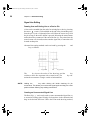
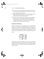
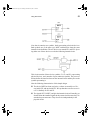
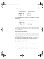
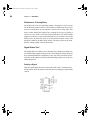
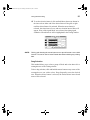
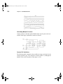
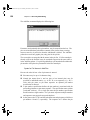
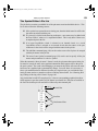
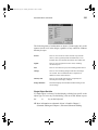
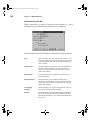
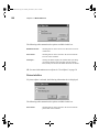
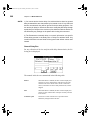
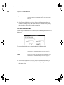
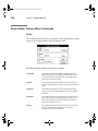
LW Reference.bk Page 116 Monday, December 15, 2003 5:59 PM
116
Chapter 6—Primitive Devices
Shift Register
The shift register is an N–bit, positive-edge–triggered device with serial or
optional parallel load. When the Shift/Load input is low, data from the N
parallel data input lines is transferred to the outputs on the rising edge of
the next clock. When Shift/Load is high, the next rising clock edge causes
the value at the Shift In input (SI) to become the new value for output Q0,
as Q0 shifts to Q1, Q1 to Q2, etc., and the old value at the most significant
output is lost.
The following table shows the shift register primitive with and without parallel inputs.
With Parallel Load
NOTE:
Without Parallel Load
The Shift Register primitive cannot be created without data outputs (that is,
as a parallel–in, serial–out register) because the flip–flop values are stored
on the output pins. Primitive devices have no internal state storage. See
more comments on this in Chapter 7, Simulation.
Clock
The clock oscillator is used to generate a repeating signal to activate other
devices. When it is first created, the clock output pin will be low; then after
a delay time called the “low time,” it will change to the high state. After a
further delay called the “high time,” the signal will revert to low and the
cycle will repeat. The low and high times are initially set to 10, but can be
modified:
Windows—Select the Parameters command from the Simulation menu.
Macintosh—Select the Set Params command from the Simulate menu.
Any number of Clocks may exist at once with independent delay times.