1
QSSC-S4R Technical Product Specification
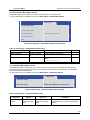
Contents
QSSC-S4R Technical Product Specification
Revision 1.0
September 14, 2010
i
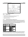
Revision History
Date
Revision Number
Modifications
Sept. 14, 2010
1.0
First release
Disclaimer
Information in this document is provided in connection with Server System QSSC-S4R manufactured by Quanta
Computer Inc. No license, express or implied, by estoppel or otherwise, to any intellectual property rights is granted
by this document. Except as provided in Quanta’s Terms and Conditions of Sale for such products, Quanta assumes
no liability whatsoever, and Quanta disclaims any express or implied warranty, relating to sale and/or use of QSSCS4R products including liability or warranties relating to fitness for a particular purpose, merchantability, or
infringement of any patent, copyright or other intellectual property right. QSSC-S4R products are not intended for use
in medical, life saving, or life sustaining applications. Quanta may make changes to specifications and product
descriptions at any time, without notice.
Designers must not rely on the absence or characteristics of any features or instructions marked "reserved" or
"undefined." Quanta reserves these for future definition and shall have no responsibility whatsoever for conflicts or
incompatibilities arising from future changes to them.
This document contains information on products in the design phase of development. Do not finalize a design with
this information. Revised information will be published when the product is available. Verify with your local sales
office that you have the latest datasheet before finalizing a design.
The QSSC-S4R Server System may contain design defects or errors known as errata which may cause the product
to deviate from published specifications. Current characterized errata are available on request.
* Intel and Xeon are trademarks or registered trademarks of Intel Corporation.
* Other brands and names may be claimed as the property of others.
Copyright © Quanta Computer Inc. 2010. All rights reserved.
ii
QSSC-S4R Technical Product Specification
Contents
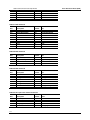
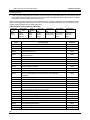
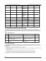
Contents
1. Introduction .............................................................................................................................. 21
1.1 Document Organization .......................................................................................................................................... 21
1.2 System Overview.................................................................................................................................................... 21
1.3 System Features .................................................................................................................................................... 21
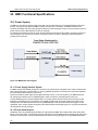
2. Main Board .............................................................................................................................. 23
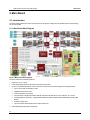
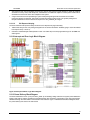
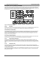
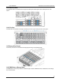
2.1 Introduction ............................................................................................................................................................. 23
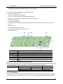
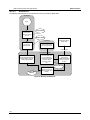
2.1.1 Main Board Block Diagram ............................................................................................................................................... 23
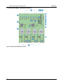
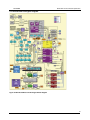
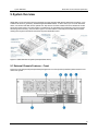
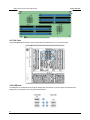
2.1.2 Main Board Major Component Placement........................................................................................................................ 25
2.2 Functional Architecture ........................................................................................................................................... 27
2.2.1 Intel® Xeon® 7500 Processors ........................................................................................................................................ 27
2.2.2 Intel® 7500 Chipset .......................................................................................................................................................... 30
2.2.3 Intel® 7500 Scalable Memory Buffer ................................................................................................................................ 32
2.2.4 ICH10R Southbridge ........................................................................................................................................................ 33
2.2.5 PCI-Express Subsystem .................................................................................................................................................. 36
2.2.6 Main Board Memory Riser Interface ................................................................................................................................. 36
2.2.7 Main Board I/O Riser Interface ......................................................................................................................................... 36
2.2.8 SAS Sub-System Interface ............................................................................................................................................... 37
2.2.9 Clock Subsystem.............................................................................................................................................................. 37
2.2.10 Serial-ATA (SATA) Sub-system ..................................................................................................................................... 40
2.2.11 BIOS Flash Devices ....................................................................................................................................................... 40
2.2.12 USB 2.0 Subsystem ....................................................................................................................................................... 40
2.2.13 Post Code LEDs ............................................................................................................................................................. 41
2.2.14 Programmable Logic Devices (PLDs) ............................................................................................................................ 41
2.2.15 Interrupt and Error Logic Block Diagram ........................................................................................................................ 42
2.2.16 Power Delivery Block Diagram ....................................................................................................................................... 42
2.2.17 Reset and Powergood Diagram ..................................................................................................................................... 44
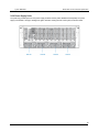
2.2.18 Power Sequencing/Timing Diagrams ............................................................................................................................. 45
2.2.19 Thermal Specifications ................................................................................................................................................... 45
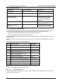
3. Main Board Server Management ............................................................................................. 47
3.1 Introduction ............................................................................................................................................................. 47
3.1.1 IPMI 2.0 Features ............................................................................................................................................................. 47
3.1.2 Non IPMI Features ........................................................................................................................................................... 48
3.2 Functional Architecture ........................................................................................................................................... 49
3.2.1 Server Management Block Diagram................................................................................................................................. 49
3.2.2 SMBus Block Diagram ..................................................................................................................................................... 50
3.2.3 Hardware Monitoring Block Diagram ................................................................................................................................ 51
3.2.4 Sensor Data Record SDR (SDR) Repository ................................................................................................................... 51
3.2.5 Field Replaceable Unit (FRU) Inventory Devices ............................................................................................................. 51
3.2.6 System Event Log (SEL) .................................................................................................................................................. 52
3.2.7 Real-Time Clock (RTC) Access........................................................................................................................................ 52
3.3 Supported Features ................................................................................................................................................ 52
3.3.1 Fan Speed Control ........................................................................................................................................................... 52
3.3.2 PECI ................................................................................................................................................................................. 52
3.3.3 CPU Throttling .................................................................................................................................................................. 52
3.3.4 Memory Throttling ............................................................................................................................................................ 53
iii
3.3.5 Chassis Intrusion .............................................................................................................................................................. 53
4. Memory Riser .......................................................................................................................... 54
4.1 System Memory Topology and Functional Diagram .............................................................................................. 54
4.2 Intel® 7500 Scalable Memory Buffer (Mill Brook) Functionality ............................................................................. 55
4.2.1 Intel® Scalable Memory Interconnect Functionality ......................................................................................................... 55
4.2.2 DDR3 Functionality .......................................................................................................................................................... 56
4.3 Functional Architecture ........................................................................................................................................... 57
4.3.1 Supported Memory Configurations ................................................................................................................................... 57
4.3.2 Temperature Sensors, FRU, and SPD ............................................................................................................................. 58
4.3.3 Memory Riser LEDs ......................................................................................................................................................... 58
4.3.4 Power Rails ...................................................................................................................................................................... 58
5. I/O Riser................................................................................................................................... 59
5.1 I/O Riser Features .................................................................................................................................................. 59
5.2 Functional Architecture ........................................................................................................................................... 60
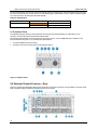
5.3 Video Subsystem.................................................................................................................................................... 60
5.3.1 Feature Overview ............................................................................................................................................................. 60
5.3.2 ServerEngines Pilot II IBMC Block Diagram ..................................................................................................................... 61
5.3.3 Video Disable Feature ...................................................................................................................................................... 61
5.3.4 Dual Video ........................................................................................................................................................................ 61
5.4 USB Subsystem ..................................................................................................................................................... 61
6. Intel® Remote Management Module 3 (RMM3) ...................................................................... 63
7. SAS Riser ................................................................................................................................ 65
7.1 Introduction ............................................................................................................................................................. 65
7.1.1 SAS Riser Features.......................................................................................................................................................... 65
7.2 Functional Architecture ........................................................................................................................................... 65
7.2.1 I²C Interface ..................................................................................................................................................................... 66
7.2.2 Host Interface ................................................................................................................................................................... 66
7.2.3 Internal SAS Interface ...................................................................................................................................................... 66
7.2.4 Memory Interface ............................................................................................................................................................. 67
7.2.5 Debug Jumpers ................................................................................................................................................................ 67
7.2.6 iBBU07 Remote Battery Backup for On-board Memory (optional) ................................................................................... 67
7.2.7 SAS Riser Power.............................................................................................................................................................. 67
8. Hot Swap Backplane (HSBP) .................................................................................................. 68
8.1 Introduction ............................................................................................................................................................. 68
8.1.1 Key Features .................................................................................................................................................................... 68
8.1.2 Placement View and LED Definition ................................................................................................................................. 69
8.1.3 Connector Signal Description and Pin-outs ...................................................................................................................... 70
8.2 Functional Architecture ........................................................................................................................................... 71
8.2.1 SAS Buses ....................................................................................................................................................................... 72
8.2.2 Hot-swap Backplane ........................................................................................................................................................ 72
8.2.3 Full-duplex Serial Mode Operation ................................................................................................................................... 72
8.2.4 SAS Controller.................................................................................................................................................................. 72
8.2.5 Vitesse* VSC410 Controller Functionality ........................................................................................................................ 73
8.2.6 SAS Drive Functionality .................................................................................................................................................... 73
8.2.7 Power Control Interlock .................................................................................................................................................... 73
8.2.8 SAS Enclosure Management ........................................................................................................................................... 74
8.2.9 Server Management Interface .......................................................................................................................................... 74
8.2.10 Resets ............................................................................................................................................................................ 75
8.2.11 Clock Generation............................................................................................................................................................ 75
8.2.12 Programmed Devices ..................................................................................................................................................... 75
9. System Overview ..................................................................................................................... 76
iv
QSSC-S4R Technical Product Specification
Contents
9.1 External Chassis Features – Front ......................................................................................................................... 76
9.1.1 Fan Subsystem ................................................................................................................................................................ 78
9.1.2 Operator Panel ................................................................................................................................................................. 79
9.2 External Chassis Features – Rear ......................................................................................................................... 79
9.3 Power Subsystem................................................................................................................................................... 80
9.3.1 Power Distribution Board (PDB) ....................................................................................................................................... 82
9.4 Cooling Subsystem................................................................................................................................................. 83
9.5 Specifications ......................................................................................................................................................... 83
9.5.1 Environmental Specifications ........................................................................................................................................... 83
9.5.2 Physical Specifications ..................................................................................................................................................... 84
9.6 Component Enumeration ....................................................................................................................................... 84
9.6.1 Processors & IOHs ........................................................................................................................................................... 84
9.6.2 Fans ................................................................................................................................................................................. 85
9.6.3 Hard Drive Slots ............................................................................................................................................................... 86
9.6.4 PCIe Slots ........................................................................................................................................................................ 86
9.6.5 Memory Riser Boards ....................................................................................................................................................... 86
9.6.6 DIMM Slots on Memory Board ......................................................................................................................................... 86
9.6.7 NIC Ports .......................................................................................................................................................................... 87
9.6.8 USB Ports ........................................................................................................................................................................ 87
9.6.9 Power Supply Units .......................................................................................................................................................... 88
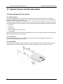
10.
System Chassis and Sub-Assemblies .................................................................................. 89
10.1 Base Chassis and Top Covers ............................................................................................................................. 89
10.1.1 Base Chassis ................................................................................................................................................................. 89
10.1.2 Top Cover ...................................................................................................................................................................... 89
10.1.3 Slide Rails ...................................................................................................................................................................... 89
10.1.4 Cable Management Arm ................................................................................................................................................ 90
10.2 Power and Fan Subsystems ................................................................................................................................ 90
10.2.1 Power Supply Modules ................................................................................................................................................... 91
10.2.2 Fan Subsystem .............................................................................................................................................................. 92
10.3 Main Board Subsystem ........................................................................................................................................ 94
10.4 Peripheral Bay Subsystem ................................................................................................................................... 96
10.4.1 Hard Drive Carrier .......................................................................................................................................................... 96
10.4.2 Optical Drive ................................................................................................................................................................... 97
10.4.3 5 ¼” Tape Drive Bay ...................................................................................................................................................... 98
11.
Cables and Connectors ........................................................................................................ 99
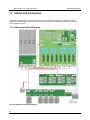
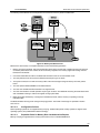
11.1 Interconnect Block Diagram ................................................................................................................................. 99
11.2 Cable and Interconnect Descriptions ................................................................................................................. 100
11.3 User-Accessible Interconnects ........................................................................................................................... 101
11.3.1 Serial Port .................................................................................................................................................................... 101
11.3.2 Video Ports ................................................................................................................................................................... 102
11.3.3 Universal Serial Bus (USB) Interface ........................................................................................................................... 102
12.
850W Power Supply ........................................................................................................... 104
12.1 Mechanical Outline ............................................................................................................................................. 104
12.2 Low Profile Hybrid Interconnect Connector ........................................................................................................ 104
12.3 AC Input Requirement ........................................................................................................................................ 105
12.3.1 AC Input Voltage Specification ..................................................................................................................................... 105
12.3.2 Efficiency ...................................................................................................................................................................... 105
12.3.3 Input Over-Current Protection ...................................................................................................................................... 105
12.3.4 Inrush Current .............................................................................................................................................................. 105
12.3.5 Auto Restart ................................................................................................................................................................. 105
12.3.6 Power Factor Correction (PFC) .................................................................................................................................... 106
12.3.7 AC Input Connector ...................................................................................................................................................... 106
12.4 DC Output Requirements ................................................................................................................................... 106
12.4.1 Hot Swap Functionality................................................................................................................................................. 106
v
12.4.2 Output Current Rating .................................................................................................................................................. 106
12.4.3 Over- and Under-Voltage Protection ............................................................................................................................ 106
12.4.4 Short Circuit Protection ................................................................................................................................................ 107
12.4.5 Over Temperature Protection ....................................................................................................................................... 107
12.4.6 Reset After Shutdown .................................................................................................................................................. 107
12.4.7 Current Sharing ............................................................................................................................................................ 107
12.4.8 I2C Devices .................................................................................................................................................................. 107
12.4.9 Module Cold Redundancy Operation ........................................................................................................................... 107
12.4.10 Power Supply Module LED indicators ........................................................................................................................ 108
12.5 Regulatory Agency Requirements...................................................................................................................... 108
13.
Power Distribution Board (PDB) ......................................................................................... 109
13.1 Introduction ......................................................................................................................................................... 109
13.2 Functional Block Diagram and Feature Description ........................................................................................... 110
13.2.1 Connector Signal Description and Pin-outs .................................................................................................................. 111
13.2.2 Voltage Regulation ....................................................................................................................................................... 114
13.2.3 DC Output Load Requirements .................................................................................................................................... 114
13.2.4 Dynamic Loading.......................................................................................................................................................... 115
13.2.5 Protection Circuits ........................................................................................................................................................ 115
13.2.6 Remote On/Off (PSON*) .............................................................................................................................................. 115
13.2.7 PSKILL ......................................................................................................................................................................... 115
13.2.8 POWER GOOD SIGNAL (PWOK) ............................................................................................................................... 115
13.2.9 SMBAlert# .................................................................................................................................................................... 115
13.2.10 PMBus Requirements ................................................................................................................................................ 116
13.3 Cold Redundant Operation................................................................................................................................. 116
13.3.1 PDB Cold Redundancy Control Circuitry ...................................................................................................................... 116
13.3.2 Cold Redundancy Functional Description .................................................................................................................... 117
13.3.3 Cold Redundancy Disabling Feature ............................................................................................................................ 118
14.
Front Panel Fan Board (FPFB) and Operator Panel .......................................................... 119
14.1 Architectural Overview ....................................................................................................................................... 119
14.2 Front Panel Fan Board (FPFB) Functional Architecture .................................................................................... 120
14.2.1 Front Panel Fan Board (FPFB) Connector Signal Description and Pinouts ................................................................. 120
14.2.2 LED Description ........................................................................................................................................................... 123
14.3 Front Panel Control ............................................................................................................................................ 123
14.3.1 System ID Buttons and LEDs ....................................................................................................................................... 123
14.3.2 Functional Block Diagram ............................................................................................................................................ 125
14.3.3 Connector Definition and Pinout ................................................................................................................................... 125
15.
Basic Input/Output System (BIOS) ..................................................................................... 126
15.1 BIOS Architecture ............................................................................................................................................... 126
15.1.1 Data Structure Descriptions ......................................................................................................................................... 126
15.2 BIOS Identification String ................................................................................................................................... 126
16.
BIOS Initialization ............................................................................................................... 127
16.1 Processors.......................................................................................................................................................... 127
16.1.1 CPUID .......................................................................................................................................................................... 127
16.1.2 Multiple Processor Initialization .................................................................................................................................... 127
16.1.3 CPU Population ............................................................................................................................................................ 127
16.1.4 Mixed Processor Steppings .......................................................................................................................................... 128
16.1.5 Mixed Processor Families ............................................................................................................................................ 128
16.1.6 Mixed Processor Intel® QuickPath Interconnect Speeds ............................................................................................. 128
16.1.7 Mixed Processor Cache Sizes ..................................................................................................................................... 128
16.1.8 Processor Cache .......................................................................................................................................................... 128
16.1.9 Microcode Update ........................................................................................................................................................ 128
16.1.10 Mixed Processor Configuration .................................................................................................................................. 128
16.1.11 Intel® Hyper-Threading Technology........................................................................................................................... 130
vi
QSSC-S4R Technical Product Specification
Contents
16.1.12 Enhanced Intel SpeedStep® Technology................................................................................................................... 130
16.1.13 Intel® 64 Instruction Set Architecture (Intel® 64) ....................................................................................................... 130
16.1.14 Execute Disable Bit Feature ....................................................................................................................................... 130
16.1.15 Enhanced Halt State (C1E) ........................................................................................................................................ 131
16.1.16 Hardware Prefetcher .................................................................................................................................................. 131
16.1.17 Adjacent Cache Line Prefetch .................................................................................................................................... 131
16.1.18 Multi-Core Processor Support .................................................................................................................................... 131
16.1.19 Intel® Virtualization Technology ................................................................................................................................. 131
16.1.20 Direct Cache Access (DCA) ....................................................................................................................................... 131
16.1.21 Intel® Turbo Boost Technology .................................................................................................................................. 131
16.1.22 Acoustical Fan Speed Control .................................................................................................................................... 132
16.1.23 CPU Core Error Handling ........................................................................................................................................... 132
16.1.24 Cbox Error Records.................................................................................................................................................... 132
16.2 Memory............................................................................................................................................................... 133
16.2.1 Memory Sizing and Configuration ................................................................................................................................ 134
16.2.2 POST Error Codes ....................................................................................................................................................... 134
16.2.3 Displaying System Memory .......................................................................................................................................... 135
16.2.4 Support for Mixed-speed Memory Modules .................................................................................................................. 135
16.2.5 Memory Test ................................................................................................................................................................ 136
16.2.6 Memory Scrub Engine .................................................................................................................................................. 136
16.2.7 Memory Map and Population Rules ............................................................................................................................. 136
16.2.8 Memory Sub-System Nomenclature............................................................................................................................. 137
16.2.9 Supported Memory Configurations ............................................................................................................................... 141
16.2.10 Modes of Operation – Memory RAS Features............................................................................................................ 142
16.2.11 Memory Hot-Plug ....................................................................................................................................................... 148
16.2.12 Memory Error Handling .............................................................................................................................................. 152
16.3 Peripheral Component Interconnect (PCI) ......................................................................................................... 168
16.3.1 Scan Order ................................................................................................................................................................... 168
16.3.2 Resource Assignment .................................................................................................................................................. 169
16.3.3 Automatic IRQ Assignment .......................................................................................................................................... 169
16.3.4 EFI Optimized Boot support and Legacy Option ROMs ............................................................................................... 169
16.3.5 EFI PCI APIs ................................................................................................................................................................ 169
16.3.6 Legacy PCI APIs .......................................................................................................................................................... 169
16.3.7 Dual Video .................................................................................................................................................................... 169
16.4 PnP ISA .............................................................................................................................................................. 169
16.5 Keyboard / Mouse .............................................................................................................................................. 169
16.6 Universal Serial Bus (USB) ................................................................................................................................ 169
16.6.1 Native USB Support ..................................................................................................................................................... 170
16.6.2 Legacy USB Support .................................................................................................................................................... 170
16.6.3 SAS Supprt ................................................................................................................................................................... 170
16.7 Removable Media Drives ................................................................................................................................... 170
16.7.1 DIMM Thermal Management ........................................................................................................................................ 170
16.8 PCI Express Hot Plug ......................................................................................................................................... 170
16.9 Fan Speed Control and Thermal Management .................................................................................................. 172
16.9.1 DIMM Thermal Management ........................................................................................................................................ 172
16.9.2 Processor Thermal Management ................................................................................................................................. 175
16.9.3 Node Power Thermal Management (NPTM) or Node Manager (NM) .......................................................................... 175
17.
BIOS User Interface ........................................................................................................... 176
17.1 Splash Logo / Diagnostic Screen ....................................................................................................................... 176
17.1.1 BIOS Boot Popup Menu ............................................................................................................................................... 176
17.2 BIOS Setup Utility ............................................................................................................................................... 176
17.2.1 Operation ..................................................................................................................................................................... 176
17.2.2 Page Layout ................................................................................................................................................................. 176
17.2.3 BIOS Setup Utility Screens .......................................................................................................................................... 178
17.3 Loading BIOS Defaults ....................................................................................................................................... 207
17.4 Clearing the BIOS Password ..............................................................................................................................207
vii
18.
BIOS Update Support......................................................................................................... 208
18.1 BIOS Update and Recovery ............................................................................................................................... 208
18.1.1 Performing BIOS Recovery .......................................................................................................................................... 208
18.2 OEM Binary ........................................................................................................................................................ 208
18.2.1 OEM Splash Logo ........................................................................................................................................................ 208
19.
Operating System Boot, Sleep, and Wake ......................................................................... 209
19.1 Boot Device Selection ........................................................................................................................................ 209
19.1.1 Server Management Boot Device Control .................................................................................................................... 209
19.1.2 USB Boot Device Reordering ....................................................................................................................................... 209
19.1.3 Boot Order Table .......................................................................................................................................................... 210
19.2 Operating System Support ................................................................................................................................. 214
19.2.1 Microsoft Windows* Compatibility ................................................................................................................................ 214
19.2.2 Advanced Configuration and Power Interface (ACPI) .................................................................................................. 214
19.2.3 Windows Hardware Error Architecture (WHEA) ........................................................................................................... 216
19.2.4 EFI Optimized Boot ...................................................................................................................................................... 217
19.2.5 Intel® Turbo Boost Technology .................................................................................................................................... 218
19.3 Front Control Panel Support ............................................................................................................................... 218
19.3.1 Power Button ................................................................................................................................................................ 218
19.3.2 Reset Button ................................................................................................................................................................ 218
19.3.3 NMI Button ................................................................................................................................................................... 218
19.4 Sleep and Wake Support ................................................................................................................................... 218
19.4.1 System Sleep States .................................................................................................................................................... 218
19.4.2 Wake Events / SCI Sources ......................................................................................................................................... 219
19.5 Non-Maskable Interrupt (NMI) Handling............................................................................................................. 219
20.
BIOS Role in Server Management ..................................................................................... 220
20.1 IPMI .................................................................................................................................................................... 220
20.2 Console Redirection ........................................................................................................................................... 220
20.2.1 Serial Configuration Settings ........................................................................................................................................ 220
20.2.2 Keystroke Mappings ..................................................................................................................................................... 220
20.2.3 Limitations .................................................................................................................................................................... 221
20.2.4 Interface to Server Management .................................................................................................................................. 221
20.3 IPMI Serial Interface ........................................................................................................................................... 221
20.3.1 Channel Access Modes ................................................................................................................................................ 221
20.3.2 Interaction with BIOS Console Redirection .................................................................................................................. 221
20.3.3 Multi-Core Intel® Xeon® Processor-based Server SOL, EMP and Console Redirection Use Case Model ................. 222
20.4 Wired For Management (WFM) .......................................................................................................................... 222
20.4.1 Preboot eXecution Environment (PXE) BIOS Support ................................................................................................. 222
20.5 System Management BIOS (SMBIOS) .............................................................................................................. 223
20.5.1 Access Methods ........................................................................................................................................................... 223
20.5.2 SMBIOS Structures Supported..................................................................................................................................... 223
20.6 Security............................................................................................................................................................... 231
20.6.1 BIOS Setup Password Protection................................................................................................................................. 231
20.6.2 Password Clear Jumper ............................................................................................................................................... 231
20.6.3 Trusted Platform Module (TPM) Security ..................................................................................................................... 231
21.
BIOS Error Handling........................................................................................................... 233
21.1 Fault Resilient Booting ....................................................................................................................................... 233
21.1.1 BSP POST Failure (FRB-2) .......................................................................................................................................... 233
21.1.2 Operating System Load Failure (OS Boot Timer) ......................................................................................................... 233
21.1.3 Operating System Watchdog Failure............................................................................................................................ 234
21.1.4 Boot Event .................................................................................................................................................................... 234
21.2 Error Handling and Logging ............................................................................................................................... 234
21.2.1 Error Sources and Types ............................................................................................................................................. 234
21.2.2 NMI on Fatal Errors ...................................................................................................................................................... 235
21.2.3 Error Logging via SMI Handler ..................................................................................................................................... 235
viii
QSSC-S4R Technical Product Specification
Contents
21.2.4 Logging Format Conventions ....................................................................................................................................... 241
21.3 POST Progress Codes and Errors ..................................................................................................................... 242
21.3.1 Diagnostic LEDs ........................................................................................................................................................... 242
21.3.2 POST Code Checkpoints ............................................................................................................................................. 242
21.3.3 POST Error Manager Messages and Handling ............................................................................................................ 244
21.3.4 POST Error Beep Codes .............................................................................................................................................. 246
21.3.5 POST Error Pause Option ............................................................................................................................................ 247
22.
Baseboard Management Controller (BMC) ........................................................................ 248
22.1 Feature Support.................................................................................................................................................. 248
22.1.1 IPMI 2.0 Features ......................................................................................................................................................... 248
22.1.2 Non IPMI Features ....................................................................................................................................................... 248
22.1.3 Basic and Advanced Features ..................................................................................................................................... 249
22.2 BMC Hardware: ServerEngines* Pilot II ............................................................................................................. 249
22.2.1 ServerEngines* Pilot II Baseboard Management Controller Functionality .................................................................... 249
23.
BMC Functional Specifications ........................................................................................... 251
23.1 Power System .................................................................................................................................................... 251
23.1.1 Power Supply Interface Signals ................................................................................................................................... 251
23.1.2 Power-Good Dropout ................................................................................................................................................... 251
23.1.3 Power up Sequence ..................................................................................................................................................... 252
23.1.4 Power Down Sequence ................................................................................................................................................ 252
23.1.5 Power Control Sources ................................................................................................................................................ 252
23.1.6 Power State Retention ................................................................................................................................................. 253
23.1.7 Power State Restoration .............................................................................................................................................. 253
23.1.8 Wake-On-LAN (WOL) .................................................................................................................................................. 253
23.2 Advanced Configuration and Power Interface (ACPI) ........................................................................................ 253
23.2.1 ACPI Power Control ..................................................................................................................................................... 254
23.2.2 ACPI State Synchronization ......................................................................................................................................... 254
23.3 System Reset Control ........................................................................................................................................ 254
23.3.1 Reset Signal Output ..................................................................................................................................................... 254
23.3.2 Reset Control Sources ................................................................................................................................................. 254
23.3.3 Front Panel System Reset ........................................................................................................................................... 255
23.3.4 Soft Reset and Hard Reset .......................................................................................................................................... 255
23.3.5 BMC Command to Cause System Reset ..................................................................................................................... 255
23.3.6 Watchdog Timer Expiration .......................................................................................................................................... 255
23.4 BMC Reset Control............................................................................................................................................. 255
23.4.1 BMC Exits Firmware Update Mode .............................................................................................................................. 255
23.4.2 Standby Power Comes Up ........................................................................................................................................... 255
23.5 System Initialization ............................................................................................................................................ 255
23.5.1 Processor TControl Setting .......................................................................................................................................... 255
23.5.2 Fault Resilient Booting (FRB) ....................................................................................................................................... 255
24.
Processor Presence and Population Check ....................................................................... 257
24.1.1 BSP Identification ......................................................................................................................................................... 257
24.1.2 Boot Control Support .................................................................................................................................................... 257
24.1.3 Post Code Display ........................................................................................................................................................ 257
24.2 Integrated Front Panel User Interface ................................................................................................................ 257
24.2.1 Power LED ................................................................................................................................................................... 257
24.2.2 System Status LED ...................................................................................................................................................... 257
24.2.3 Chassis ID LED ............................................................................................................................................................ 259
24.2.4 Front Panel / Chassis Inputs ........................................................................................................................................ 259
24.2.5 Secure Mode and Front Panel Lock-out Operation ...................................................................................................... 260
24.3 Private Management I2C Buses........................................................................................................................ 260
24.4 Watchdog Timer ................................................................................................................................................. 260
24.5 BMC Internal Timestamp Clock.......................................................................................................................... 261
24.5.1 BMC Clock Initialization ................................................................................................................................................ 261
ix
24.5.2 System Clock Synchronization ..................................................................................................................................... 261
24.6 System Event Log (SEL) .................................................................................................................................... 261
24.6.1 Servicing Events........................................................................................................................................................... 261
24.6.2 SEL Entry Deletion ....................................................................................................................................................... 261
24.6.3 SEL Erasure ................................................................................................................................................................. 261
24.7 Sensor Data Record (SDR) Repository.............................................................................................................. 261
24.7.1 SDR Repository Erasure .............................................................................................................................................. 262
24.7.2 Initialization Agent ........................................................................................................................................................ 262
24.8 Field Replaceable Unit (FRU) Inventory Device ................................................................................................ 262
24.8.1 BMC FRU Inventory Area Format ................................................................................................................................ 262
24.8.2 BMC FRU ID Mapping .................................................................................................................................................. 262
24.9 Diagnostics and Beep Code Generation ............................................................................................................ 263
24.9.1 Signal Generation......................................................................................................................................................... 263
24.10 Sensor Rearm Behavior ................................................................................................................................... 264
24.10.1 Manual vs. Rearm Sensors ........................................................................................................................................ 264
24.10.2 Rearm and Event Generation ..................................................................................................................................... 264
24.11 Processor Sensors ........................................................................................................................................... 264
24.11.1 Processor Status Sensors .......................................................................................................................................... 265
24.11.2 Processor VRD Over-Temperature Sensor ................................................................................................................ 266
24.11.3 Digital Thermal Sensor ............................................................................................................................................... 266
24.11.4 Processor Thermal Control Monitoring (Prochot) ....................................................................................................... 266
24.12 Voltage Monitoring............................................................................................................................................ 266
24.13 Standard Fan Management..............................................................................................................................267
24.13.1 Hot Swap Fans ........................................................................................................................................................... 267
24.13.2 Fan Redundancy Detection ........................................................................................................................................ 268
24.13.3 Fan Domains .............................................................................................................................................................. 268
24.13.4 Nominal Fan Speed.................................................................................................................................................... 268
24.13.5 Thermal and Acoustic Management (Acoustic Monitoring) ........................................................................................ 271
24.14 DIMM Thermal Margin Sensor ......................................................................................................................... 272
24.15 IOH thermal Margin Sensor..............................................................................................................................273
24.16 Memory Buffer Thermal Margin Sensor ........................................................................................................... 273
24.17 Add In Card Thermal Margin Sensor................................................................................................................ 273
24.18 Power Throttle Sensor ...................................................................................................................................... 273
24.19 Memory Riser Power Failure Monitoring .......................................................................................................... 274
24.20 Memory Hot Plug and Memory Offline/Online.................................................................................................. 274
24.20.1 Semaphore Operation ................................................................................................................................................ 274
24.20.2 Sequence of Operations during Memory Hot Plug ..................................................................................................... 275
24.21 HeartBeat LED ................................................................................................................................................. 276
24.22 CSS LED .......................................................................................................................................................... 277
24.23 Global Fan Fault LED ....................................................................................................................................... 277
24.24 Power Management Bus (PMBus) ................................................................................................................... 277
24.24.1 PMBus Addressing ..................................................................................................................................................... 277
24.24.2 PMBus -specific Sensor Support ................................................................................................................................ 278
24.25 Power Unit Management .................................................................................................................................. 278
24.25.2 Power Supply Fan Monitoring .................................................................................................................................... 279
24.25.3 Power Supply Fan Speed Control .............................................................................................................................. 280
24.25.4 Power Supply Failure Management ........................................................................................................................... 281
24.25.5 Power Supply Status Sensors .................................................................................................................................... 281
24.25.6 Power Unit Redundancy ............................................................................................................................................. 282
24.26 3.28 Event Message Generation and Reception ............................................................................................. 282
24.27 3.29 Event Logging Disabled Sensor ............................................................................................................... 282
24.28 3.30 SMI Timeout Sensor ................................................................................................................................. 282
24.29 BMC Self Test .................................................................................................................................................. 282
24.30 BMC Test Commands ...................................................................................................................................... 282
24.31 Component Fault LED Control ......................................................................................................................... 283
24.31.1 Set Fault Indication Command ................................................................................................................................... 283
24.31.2 DIMM Mapping for Fault Indication and Fan Control Config: ...................................................................................... 283
24.32 Hot-Swap Controller ......................................................................................................................................... 284
x
QSSC-S4R Technical Product Specification
Contents
24.32.1 Backplane Types ........................................................................................................................................................ 284
24.33 LAN Leash Event Monitoring............................................................................................................................ 284
24.34 CATERR Reporting .......................................................................................................................................... 284
24.35 CMOS Battery Monitoring ................................................................................................................................ 285
25.
BMC Messaging Interfaces ................................................................................................ 286
25.1 Channel Management ........................................................................................................................................ 286
25.2 4.2 User Model ................................................................................................................................................ 286
25.3 Sessions ............................................................................................................................................................. 287
25.4 Media Bridging.................................................................................................................................................... 288
25.5 Request / Response Protocol............................................................................................................................. 288
25.6 Host to BMC Communication Interface .............................................................................................................. 288
25.6.1 LPC / KCS Interface ..................................................................................................................................................... 288
25.6.2 Receive Message Queue ............................................................................................................................................. 289
25.6.3 SMS / SMM Status Register ......................................................................................................................................... 289
25.6.4 Server Management Software (SMS) Interface ............................................................................................................ 289
25.6.5 SMM Interface .............................................................................................................................................................. 290
25.7 IPMB Communication Interface.......................................................................................................................... 290
25.7.1 BMC as I C Master Controller on IPMB ....................................................................................................................... 290
25.7.2 IPMB LUN Routing ....................................................................................................................................................... 291
25.7.3 Management Engine IPMB .......................................................................................................................................... 291
2
25.8 IPMI Serial Feature .............................................................................................................................................. 292
25.8.1 COM Port Switching ..................................................................................................................................................... 292
25.8.2 Terminal Mode ............................................................................................................................................................. 292
25.9 LAN Interface...................................................................................................................................................... 293
25.9.1 IPMI 1.5 Messaging...................................................................................................................................................... 293
25.9.2 IPMI 2.0 Messaging...................................................................................................................................................... 293
25.9.3 RMCP / ASF Messaging .............................................................................................................................................. 294
25.9.4 BMC Embedded LAN Channels ................................................................................................................................... 294
25.9.5 BMC IP Address Configuration..................................................................................................................................... 294
25.9.6 DHCP BMC Hostname ................................................................................................................................................. 295
25.9.7 Address Resolution Protocol (ARP) ............................................................................................................................. 296
25.9.8 Internet Control Message Protocol (ICMP) ...................................................................................................................... 296
25.9.9 Virtual Local Area Network (VLAN) ................................................................................................................................ 296
25.9.10 Secure Shell (SSH) ....................................................................................................................................................... 296
25.9.11 Serial-over-LAN (SOL 2.0) ............................................................................................................................................ 296
25.9.12 Platform Event Filter (PEF) .......................................................................................................................................... 297
25.9.13 LAN Alerting ................................................................................................................................................................ 297
25.9.14 SNMP Platform Event Traps (PETs) ............................................................................................................................. 297
25.9.15 Alert Policy Table ........................................................................................................................................................ 297
25.9.16 E-mail Alerting ............................................................................................................................................................. 297
26.
BMC Flash Update ............................................................................................................. 299
26.1 Logical Firmware Image Blocks ......................................................................................................................... 299
26.2 Firmware Transfer Mode Update ....................................................................................................................... 299
26.2.1 Command Support During Firmware Transfer Mode.................................................................................................... 300
26.3 Boot Recovery Mode .......................................................................................................................................... 300
26.4 Force Firmware Update Jumper......................................................................................................................... 300
26.5 Restore Default Configuration ............................................................................................................................ 301
26.6 Fast Firmware Update over USB ....................................................................................................................... 301
27.
BIOS-BMC Interactions ...................................................................................................... 302
28.
BMC-HSC Interactions ....................................................................................................... 303
28.1 HSC Availability .................................................................................................................................................. 303
28.2 Interactions ......................................................................................................................................................... 303
29.
xi
Sensors .............................................................................................................................. 304
29.1 Sensor Type Codes ............................................................................................................................................ 304
30.
Hot-Swap Controller (HSC) Architecture ............................................................................ 313
30.1.1 I2C Interfaces ............................................................................................................................................................... 313
30.1.2 Serial Peripheral Interface (SPI) ................................................................................................................................... 313
30.1.3 GPIO Pins .................................................................................................................................................................... 313
31.
HSC Functional Specifications ........................................................................................... 314
31.1 Platform Determination ....................................................................................................................................... 314
31.1.1 Auto Detection of Platform Type................................................................................................................................... 314
31.2 System Initialization ............................................................................................................................................ 314
31.2.1 Non-Volatile Setting Initialization .................................................................................................................................. 314
31.2.2 Sensor Initialization ...................................................................................................................................................... 314
31.2.3 Cable Detection ............................................................................................................................................................ 314
31.3 System Event Log (SEL) .................................................................................................................................... 315
31.4 Sensor Data Repository (SDR) .......................................................................................................................... 315
31.5 Field Replaceable Unit (FRU) Inventory Device ................................................................................................ 315
31.5.1 HSC FRU Format ......................................................................................................................................................... 315
31.6 Temperature Monitoring ..................................................................................................................................... 315
31.7 Disk Management............................................................................................................................................... 316
31.7.1 Drive Fault Light Control ............................................................................................................................................... 316
31.7.2 Drive Presence Detection ............................................................................................................................................. 316
31.7.3 Enclosure Temperature Sensing .................................................................................................................................. 316
31.8 Slot Status to Fault Light State Mapping ............................................................................................................ 316
32.
HSC IPMB Application and Sensors .................................................................................. 317
32.1 LUNs ................................................................................................................................................................... 317
32.2 Sensors .............................................................................................................................................................. 317
32.2.1 Digital and Discrete Sensor Formats ............................................................................................................................ 318
32.3 Event Message Generation ................................................................................................................................ 318
33.
HSC Firmware Update ....................................................................................................... 319
33.1 HSC Update Over IPMB ..................................................................................................................................... 319
33.1.1 Entering Firmware Transfer Mode ................................................................................................................................ 319
33.1.2 Exiting Firmware Transfer Mode .................................................................................................................................. 319
33.1.3 Firmware Transfer Version ........................................................................................................................................... 319
33.1.4 Verifying Entry Into Firmware Transfer Mode ............................................................................................................... 319
33.1.5 Set Program Segment Command ................................................................................................................................ 319
33.1.6 FLASH Erase and Sequential Programming ................................................................................................................ 319
33.1.7 Access to Operational Mode Commands ..................................................................................................................... 319
xii
QSSC-S4R Technical Product Specification
List of Figures
List of Figures
Figure 1 Main Board Block Diagram ................................................................................................................................. 23
Figure 2. Main Board Component Locations .................................................................................................................... 25
Figure 3 Intel® 7500 Chipset High-Level Block Diagram ................................................................................................. 31
Figure 4. Main Board Clock Block Diagram ...................................................................................................................... 39
Figure 5. USB 2.0 Subsystem Functional Block Diagram ................................................................................................ 40
Figure 6. Interrupt and Error Logic Block Diagram ........................................................................................................... 42
Figure 7. Mainboard Power Block Diagram ...................................................................................................................... 43
Figure 8. Main Board Reset and Powergood Block Diagram ........................................................................................... 44
Figure 9. Main Board Power Sequencing Diagram .......................................................................................................... 45
Figure 10. Server Management Block Diagram ............................................................................................................... 49
Figure 11. SMBus Block Diagram..................................................................................................................................... 50
Figure 12. Hardware Monitoring Block Diagram............................................................................................................... 51
Figure 13. QSSC-S4R System Memory Topology ........................................................................................................... 54
Figure 14. QSSC-S4R Memory Riser Functional Block Diagram and DIMM Population Rules ...................................... 55
Figure 15. DDR3 Interlace Block Diagram ....................................................................................................................... 56
Figure 16 Memory Riser Block Diagram .......................................................................................................................... 57
Figure 17. I/O Riser Block Diagram .................................................................................................................................. 60
Figure 18. ServerEngines* Pilot II IBMC Block Diagram .................................................................................................. 61
Figure 19 Integrated BMC with Intel® RMM3 Block Diagram .......................................................................................... 63
Figure 20. SAS Riser Board System Block Diagram ........................................................................................................ 66
Figure 21. SAS Riser Board Placement View .................................................................................................................. 67
Figure 22. HSBP – Front View and Hard Drive Connectors 0 – 7 .................................................................................... 69
Figure 23. HSBP – Rear View .......................................................................................................................................... 69
Figure 24. HSBP System Block Diagram ......................................................................................................................... 72
Figure 25. VSC410 Block Diagram ................................................................................................................................... 73
Figure 26. Hot-swap Backplane Reset and Power Good Block Diagram ........................................................................ 75
Figure 27. QSSC-S4R Server System (Enterprise SKU shown) ...................................................................................... 76
Figure 28. Front Components (Enterprise SKU) .............................................................................................................. 77
Figure 29. Front Components (Value SKU) Front Panel .................................................................................................. 77
Figure 30. Front Panel Fan Board Component Locations ................................................................................................ 78
Figure 31. Operator Panel ................................................................................................................................................ 79
Figure 32. System Rear (Enterprise SKU shown) ............................................................................................................ 80
Figure 33. Slide Rail Mounting Features .......................................................................................................................... 90
Figure 34. Slide Rail mounted on the System Chassis with the Cable Management Arm attached at the back of the
system ...................................................................................................................................................................... 90
Figure 35. Slide Rails and Cable Management Arm (CMA) ............................................................................................. 90
Figure 36. Power Supply Unit (PSU) ................................................................................................................................ 91
Figure 37. Power Supply Indicators .................................................................................................................................. 92
xiii
Figure 38. Fan Location .................................................................................................................................................... 93
Figure 39. S4R Fan Module.............................................................................................................................................. 93
Figure 40. Fan Module Functional Block Diagram ........................................................................................................... 94
Figure 41. Main Board Mount Structure & Strengthened CPU Heat-sink ........................................................................ 95
Figure 42. Chassis Mid-brace ........................................................................................................................................... 95
Figure 43. Strengthened CPU installation on Main Board ................................................................................................ 96
Figure 44. Peripheral Area ................................................................................................................................................ 96
Figure 45. Hard Drive Carrier ........................................................................................................................................... 97
Figure 46. Optical Drive .................................................................................................................................................... 97
Figure 47. 5 1/4-inch half-height drive .............................................................................................................................. 98
Figure 48. S4R Interconnect Block Diagram .................................................................................................................... 99
Figure 49. COM Serial Port Connector ........................................................................................................................... 102
Figure 50. VGA Video Connector ................................................................................................................................... 102
Figure 51. Dual Stacked USB Connector on Rear Panel ............................................................................................... 102
Figure 52. 850W High Efficiency Power Supply Unit Drawing ....................................................................................... 104
Figure 53. Power Supply Indicators ................................................................................................................................ 108
Figure 54. Power Distribution Board Connectors ........................................................................................................... 109
Figure 55. Power Supply Numbering on the PDB .......................................................................................................... 110
Figure 56. PDB Functional Block Diagram ..................................................................................................................... 111
Figure 57. Cold Redundancy Circuit Block Diagram ...................................................................................................... 117
Figure 58. Power Sub-system Efficiency in Cold Redundant Operation ........................................................................ 118
Figure 60. Front Panel Fan Board Component Locations .............................................................................................. 120
Figure 61. Operator Panel Controls and Indicators ........................................................................................................ 124
Figure 62. Memory Topology .......................................................................................................................................... 134
Figure 63. QSSC-S4R System Memory Topology ......................................................................................................... 137
Figure 64. QSSC-S4R Memory DIMM Topology and DIMM Population Order ............................................................. 137
Figure 65. Minimum DDR-3 DIMM Population ............................................................................................................... 139
Figure 66. Population with Non-identical DDR3 DIMMs ................................................................................................. 140
Figure 67. Minimal Population for Intra Socket Mirroring ............................................................................................... 140
Figure 68. Minimal Optimal Population Upgrade for RAS Modes .................................................................................. 141
Figure 69. Incorrect population for mirroring and sparing .............................................................................................. 141
Figure 70. Lock step mode Example .............................................................................................................................. 143
Figure 71. Intra-Socket Mirroring .................................................................................................................................... 145
Figure 72. Inter-Socket Mirroring .................................................................................................................................... 146
Figure 73. Hemisphere Example .................................................................................................................................... 147
Figure 74. Mirroring in Hemisphere Mode ...................................................................................................................... 148
Figure 75. Memory Hot-Add Flow ................................................................................................................................... 149
Figure 76. Memory Hot-Remove Flow ............................................................................................................................ 150
Figure 77. PCIE hotplug flow chart ................................................................................................................................. 171
Figure 78. Setup Utility — Main Screen Display............................................................................................................. 179
Figure 79. Setup Utility — Advanced Screen ................................................................................................................. 181
Figure 80. Setup Utility — Processor Configuration Screen .......................................................................................... 182
Figure 81. Setup Utility — Memory Configuration Screen .............................................................................................. 185
Figure 82. Setup Utility — Configure Memory RAS and Performance Screen .............................................................. 186
Figure 83. Setup Utility — Memory Riser Board Information Screens ........................................................................... 187
xiv
QSSC-S4R Technical Product Specification
List of Figures
Figure 84. Setup Utility — Mass Storage Controller Configuration Screen .................................................................... 188
Figure 85. Setup Utility — Serial Port Configuration Screen .......................................................................................... 189
Figure 86. Setup Utility — USB Configuration Screen ................................................................................................... 190
Figure 87. Setup Utility — PCI Configuration Screen ..................................................................................................... 191
Figure 88. Setup Utility — System Acoustic and Performance Configuration ................................................................ 192
Figure 89. Setup Utility — Security Screen .................................................................................................................... 193
Figure 90. Setup Utility — Server Management Screen ................................................................................................ 195
Figure 91. Setup Utility — Console Redirection Screen ................................................................................................. 196
Figure 92. Setup Utility — Server Management System Information Screen ................................................................ 197
Figure 93. Server Management - BMC Configuration .................................................................................................... 198
Figure 94. Setup Utility — Boot Options Screen ............................................................................................................ 200
Figure 95. Setup Utility — Add New Boot Option Screen Display.................................................................................. 202
Figure 96. Setup Utility — Delete Boot Option Screen Display ...................................................................................... 202
Figure 97. Setup Utility — Hard Disk Order Screen Display .......................................................................................... 203
Figure 98. Setup Utility — CDROM Order Screen ......................................................................................................... 203
Figure 99. Setup Utility — CDROM Order Screen ......................................................................................................... 203
Figure 100. Setup Utility — Network Device Order Screen ............................................................................................ 204
Figure 101. Setup Utility — BEV Device Order Screen Display ..................................................................................... 204
Figure 102. Setup Utility — Boot Manager Screen Display............................................................................................ 205
Figure 103. Setup Utility — Error Manager Screen Display ........................................................................................... 205
Figure 104. Setup Utility — Exit Screen Display ............................................................................................................ 206
Figure 105. WHEA Architectural Overview from WinHec ............................................................................................... 216
Figure 106. BMC/Power Reset Signals .......................................................................................................................... 251
Figure 107. SMBus Connections .................................................................................................................................... 260
Figure 108. Stepwise Linear Control Hysteresis ............................................................................................................ 269
Figure 109. Clamp Control Hysterisis ............................................................................................................................. 270
Figure 110. BMC/BIOS interactions for Memory Hot-Plug/On-line/Off-line Operations ................................................. 276
Figure 111. BMC IPMB Message Reception .................................................................................................................. 292
Figure 112. HSC Interface Routing................................................................................................................................. 313
xv
List of Tables
Table 1. System Features................................................................................................................................................. 21
Table 2. Mainboard components ...................................................................................................................................... 26
Table 3. Intel® Xeon® 7500 processor key features ........................................................................................................ 28
Table 4. Boxboro-EX PCI Express Port Configuration ..................................................................................................... 31
Table 5. Boxboro-EX PCI Express Port Configuration ..................................................................................................... 41
Table 6. Post LEDs and Reference Designators .............................................................................................................. 41
Table 7. QSSC-S4R Thermal Specification ...................................................................................................................... 46
Table 8. FRU Device Location and Size ........................................................................................................................... 51
Table 9. DPC Supported Configuration ............................................................................................................................ 56
The following sections describe the memory configurations that are validated on the QSSC-S4R platforms. Table 10.
QSSC-S4R Standard System DIMM Population Rules ........................................................................................... 57
Table 11. S4R Memory Riser LED Indicators ................................................................................................................... 58
Table 12. Component Description .................................................................................................................................... 69
Table 13. HDD LED Indication.......................................................................................................................................... 69
Table 14. 8X HDD Activity LED Functionality on the HSBP ............................................................................................. 70
Table 15. HSBP Control Signal Description and Pin-outs ................................................................................................ 70
Table 16. HSBP Power Connector Signal Description and Pin-outs................................................................................ 70
Table 17. HSBP Local View/ CSS Connector Signal Description and Pin-outs ............................................................... 70
Table 18. HSBP SES Connector Signal Description and Pin-outs................................................................................... 70
Table 19. 1x6-pin HSBP SATA SGPIO A – Signal Description and Pin-outs .................................................................. 71
Table 20. 1x5-pin HSBP SATA/SAS SGPIO B – Signal Description and Pin-outs .......................................................... 71
Table 21. Hot-swap Backplane Connector Specification ................................................................................................. 71
Table 22. I2C* Addresses.................................................................................................................................................. 74
Table 23. Global I2C* bus Addresses (IPMB Bus) ............................................................................................................ 75
Table 24. LED Definition ................................................................................................................................................... 79
Table 25. System rear items and descriptions ................................................................................................................. 80
Table 26. Maximum DC Loading Requirements............................................................................................................... 81
Table 27. Maximum DC Loading Requirements............................................................................................................... 81
Table 28. Maximum System Configuration Support ......................................................................................................... 81
Table 29. System Power Supply Configuration and System Load Limits ........................................................................ 82
Table 30. Environmental Specifications Summary ........................................................................................................... 83
Table 31. Physical Specifications ..................................................................................................................................... 84
Table 32. AC Input Rating ................................................................................................................................................ 91
Table 33. DC Output Voltage Regulation Limits ............................................................................................................... 91
Table 34. 850W Power Supply Load Ratings .................................................................................................................. 91
Table 35. Power supply indicators .................................................................................................................................... 92
Table 36. Fan Module Connector Signal Description and Pinouts ................................................................................... 94
Table 37. LED Definition ................................................................................................................................................... 94
Table 38. Cable Descriptions.......................................................................................................................................... 100
xvi
QSSC-S4R Technical Product Specification
List of Tables
Table 39. Connector Descriptions .................................................................................................................................. 100
Table 40. COM Serial Port Connector Pin-out (External DB9 on Rear Panel), Pedestal .............................................. 101
Table 41. VGA Video Connector Pin-out ........................................................................................................................ 102
Table 42. Dual USB Connector Pin-out (Rear).............................................................................................................. 103
Table 43. Dual USB Connector Pin-out (for uModule SSD device) ............................................................................... 103
Table 44. S4R Power Supply Connector Signal Description and Pinouts ..................................................................... 104
Table 45. AC Input Rating .............................................................................................................................................. 105
Table 46. DC Output Voltage Regulation Limits ............................................................................................................. 106
Table 47. 850W Power Supply Load Ratings ................................................................................................................. 106
Table 48. Over- and Under-Voltage Limits ..................................................................................................................... 106
Table 49. Output Current Sharing................................................................................................................................... 107
Table 50. +12V Current Sharing Requirements ............................................................................................................. 107
Table 51. Power supply indicators .................................................................................................................................. 108
Table 52. Power Distribution Board Connector Location ............................................................................................... 109
Table 53. PDB Inlet Card Edge Interface – Solder Side................................................................................................. 111
Table 54. PDB Inlet Card Edge Interface – Component Side ........................................................................................ 112
Table 55. Main Power #1 ................................................................................................................................................ 112
Table 56. Main Power #2 ................................................................................................................................................ 112
Table 57. Main Power #3 ................................................................................................................................................ 113
Table 58. Main Power #3 ................................................................................................................................................ 113
Table 59. Main Power #4 ................................................................................................................................................ 113
Table 60. 2X17-pin Power Control Connector ................................................................................................................ 113
Table 61. 2X4-pin HSBP/Fan Power Connector ............................................................................................................ 114
Table 62. Voltage Regulation Limit ................................................................................................................................. 114
Table 63. DC Output Load Ratings................................................................................................................................. 114
Table 64. Transient Load Requirements ........................................................................................................................ 115
Table 65. Over Current Protection Limits / 240VA Protection ........................................................................................ 115
Table 66. PS Enabled in Power Range .......................................................................................................................... 118
Table 67. System Fan Mapping ...................................................................................................................................... 121
Table 68. FPFB Fan Control Signal Description & Pinouts ............................................................................................ 121
Table 69. FPFB Fan Power Signal Description and Pinouts .......................................................................................... 121
Table 70. FPFB-to-HSBP (Hot-swap Backplane) Control Signal Description and Pinouts ............................................ 121
Table 71. Hot-swap Fan Signal Description and Pinouts ............................................................................................... 122
Table 72. FPFB-to-Main Board 40-Pin Connector Signal Description and Pinouts ....................................................... 122
Table 73. Front Panel Signal Description and Pinouts ................................................................................................... 122
Table 74. USB Header to Front Panel Signal Description and Pinouts.......................................................................... 123
Table 75. System ID/Temperature Combo Board Signal Description and Pinouts ........................................................ 123
Table 76. LED functionality for each LAN port at the rear .............................................................................................. 123
Table 77. System Status LED States and Operator Panel Controls .............................................................................. 124
Table 78. Front Panel Connector Definition and Pinout ................................................................................................. 125
Table 79. CPU Population Rules for QSSC-S4R ........................................................................................................... 128
Table 80. Mixed Processor Configurations .................................................................................................................... 129
Table 82. Format of Cbox Error SEL Records ................................................................................................................ 132
Table 83. Standard QSSC-S4R 4S Server Platforms DIMM Population Rules ............................................................. 142
Table 84. Memory Error Reporting Agent Summary ...................................................................................................... 153
xvii
Table 85. Memory RAS Configuration and State SEL Records for Memory Mirroring .................................................. 154
Table 86. Device Locator Nomenclature ........................................................................................................................ 155
Table 87. CPU Socket and Memory Board Grouping.................................................................................................... 155
Table 88. Formats of Memory RAS State SEL Record for Memory Mirroring ............................................................... 156
Table 89. Formats of Memory RAS State SEL Record for Memory Sparing ................................................................. 156
Table 90. Formats of Memory RAS Configuration SEL Record for Memory Mirroring .................................................. 157
Table 91. Formats of Memory RAS Configuration SEL Record for Memory Sparing .................................................... 158
Table 92. Format of Memory ECC Error SEL Records .................................................................................................. 158
Table 93. Format of Memory Mismatch Error SEL Records .......................................................................................... 159
Table 94. Format of SMI Link CRC Correctable Error SEL Records ............................................................................. 159
Table 95. Format of SMI Link CRC Uncorrectable Error SEL Records.......................................................................... 159
Table 96. Format of Patrol Scrub Error SEL Records .................................................................................................... 160
Table 97. Format of Memory Hot-plug Event SEL Records ........................................................................................... 160
Table 98. Memory Errors Captured by Error Manager ................................................................................................... 162
Table 99. DIMM Fault LED Behavior Summary ............................................................................................................. 163
Table 100. Front Panel Status LED Behavior Summary ................................................................................................ 163
Table 101. NMI Generation Summary ............................................................................................................................ 164
Table 102. Memory Error Handling — POST ................................................................................................................. 164
Table 103. Memory ECC Error Handling — Runtime, Non-Redundant Configuration................................................... 167
Table 104. Memory ECC Error Handling — Runtime, Redundant Configuration .......................................................... 168
Table 105. PCIe Bifurcation: hot-swap and non hot-swap configuration........................................................................ 171
Table 106. Set Fan Control Configuration Command Format ........................................................................................ 173
Table 107. Thermal Profile Data SDR Record Format ................................................................................................... 173
Table 108. Memory Thermal Throttling OEM SDR bytes 6:N details ............................................................................. 174
Table 109. Memory Thermal Throttling OEM SDR bytes 6:N details ............................................................................. 177
Table 110. BIOS Setup: Keyboard Command Bar ......................................................................................................... 177
Table 111. Setup Utility — Main Screen Fields .............................................................................................................. 179
Table 112. Setup Utility — Advanced Screen Display Fields ......................................................................................... 181
Table 113. Setup Utility — Processor Configuration Screen Fields ............................................................................... 183
Table 114. Setup Utility — Memory Configuration Screen Fields .................................................................................. 185
Table 115. Setup Utility — Configure RAS and Performance Screen Fields ................................................................. 186
Table 116. Setup Utility — Memory Board Information Screen Fields ........................................................................... 187
Table 117. Setup Utility — Mass Storage Controller Configuration Screen Fields ........................................................ 188
Table 118. Setup Utility — Serial Ports Configuration Screen Fields............................................................................. 189
Table 119. Setup Utility — USB Controller Configuration Screen Fields ....................................................................... 190
Table 120. Setup Utility — PCI Configuration Screen Fields ......................................................................................... 191
Table 121. Setup Utility — System Acoustic and Performance Configuration Screen Fields ........................................ 192
Table 122. Setup Utility — Security Configuration Screen Fields .................................................................................. 193
Table 123. Setup Utility — Server Management Configuration Screen Fields .............................................................. 195
Table 124. Setup Utility — Console Redirection Configuration Fields ........................................................................... 196
Table 125. Setup Utility — Server Management System Information Fields ................................................................. 197
Table 126. BMC LAN Configuration Screen Fields ........................................................................................................ 198
Table 127. Setup Utility — Boot Options Screen Fields ................................................................................................. 200
Table 128. Setup Utility — Add New Boot Option Fields ............................................................................................... 202
Table 129. Setup Utility — Delete Boot Option Fields .................................................................................................... 202
xviii
QSSC-S4R Technical Product Specification
List of Tables
Table 130. Setup Utility — Hard Disk Order Fields ........................................................................................................ 203
Table 131. Setup Utility — CDROM Order Fields .......................................................................................................... 203
Table 132. Setup Utility — CDROM Order Fields .......................................................................................................... 204
Table 133. Setup Utility — Network Device Order Fields ............................................................................................... 204
Table 134. Setup Utility — BEV Device Order Fields ..................................................................................................... 205
Table 135. Setup Utility — Boot Manager Screen Fields ............................................................................................... 205
Table 136. Setup Utility — Error Manager Screen Fields .............................................................................................. 205
Table 137. Setup Utility — Exit Screen Fields ................................................................................................................ 206
Table 138. Overall Boot Order Table (BOT) Structure ................................................................................................... 210
Table 139. Boot Order Table Header Structure.............................................................................................................. 210
Table 140. BOT Order Table Structure .......................................................................................................................... 210
Table 141. BOT Non-EFI Order Tables .......................................................................................................................... 212
Table 142. BOT EFI Device Order Table ....................................................................................................................... 213
Table 143. BOT Non-EFI Device Name Structure.......................................................................................................... 213
Table 144. BOT EFI Device Name and Path Structure .................................................................................................. 213
Table 145. Minimal Boot Order Table Structure ............................................................................................................. 214
Table 146. Supported ACPI Tables ................................................................................................................................ 215
Table 147. NMI Error Messages ..................................................................................................................................... 219
Table 148. Console Redirection Escape Sequences for Headless Operation ............................................................... 221
Table 149. SMBIOS Table Structure for Locating SMBIOS Tables ............................................................................... 223
Table 150. SMBIOS Type 0 Structure ............................................................................................................................ 224
Table 151. SMBIOS Type 1 Structure ............................................................................................................................ 224
Table 152. SMBIOS Type 4 Structure ............................................................................................................................ 225
Table 153. SMBIOS Type 7 Structure ............................................................................................................................ 226
Table 154. SMBIOS Type 11 Structure .......................................................................................................................... 227
Table 155. SMBIOS Type 13 Structure .......................................................................................................................... 228
Table 156. SMBIOS Type 16 Structure .......................................................................................................................... 228
Table 157. SMBIOS Type 17 Structure .......................................................................................................................... 228
Table 158. SMBIOS Type 38 Structure .......................................................................................................................... 230
Table 160. OS/SMS Watchdog Timeout SEL Events..................................................................................................... 234
Table 161. Standard AER Fatal Errors ........................................................................................................................... 236
Table 162. Standard AER Correctable Errors ................................................................................................................ 237
Table 163. Legacy PCI Sensors ..................................................................................................................................... 238
Table 164. Intel® QuickPath Interconnect Errors .......................................................................................................... 239
Table 165. FRB-2 Timeout SEL Events ......................................................................................................................... 240
Table 166. OS Boot Timeout SEL Events ...................................................................................................................... 240
Table 167, OS/SMS Watchdog Timeout SEL Events..................................................................................................... 241
Table 168. Example – SEL Log Data For An FRB-2 Error Event................................................................................... 241
Table 169. Post Codes and Messages ........................................................................................................................... 242
Table 170. SEL Format for POST Error Messages ........................................................................................................ 245
Table 171. POST Error Messages and Handling ........................................................................................................... 245
Table 172. POST Error Beep Codes .............................................................................................................................. 247
Table 173. Basic and Advanced Features...................................................................................................................... 249
Table 174. Power Control Sources ................................................................................................................................. 252
Table 175. ACPI States .................................................................................................................................................. 253
xix
Table 176. System Status LED Indicator States ............................................................................................................ 258
Table 177. List of I2C Buses ........................................................................................................................................... 260
Table 178. FRU Device ID Map ...................................................................................................................................... 262
Table 179. BMC Beep Codes ......................................................................................................................................... 263
Table 180. NMI Signal Generation and Event Logging .................................................................................................. 264
Table 181. Processor Sensors ....................................................................................................................................... 265
Table 182. Processor Status Sensor Implementation .................................................................................................... 265
Table 183. Fan Profile Mapping...................................................................................................................................... 271
Table 184. PMBus D Device Addressing ....................................................................................................................... 277
Table 185. Power Unit Sensor Offsets ........................................................................................................................... 278
Table 186. Supported Sensor Offsets ............................................................................................................................ 280
Table 187. Example PS Fan Lookup Table .................................................................................................................... 280
Table 188. Power Supply Sensor Offsets ....................................................................................................................... 281
Table 189. BMC Self Test Results.................................................................................................................................. 282
Table 190 shows outputs that can be tested via the Set SM Signal command. ............................................................ 283
Table 191. Set SM Signal Command Signal Definition .................................................................................................. 283
Table 192 shows the inputs (buttons / switches) that can be tested via the Get SM Signal command. ........................ 283
Table 193. Get SM Signal Command Signal Definition .................................................................................................. 283
Table 194. Standard Channel Assignments ................................................................................................................... 286
Table 195. QSSC-S4R Channel Assignment ................................................................................................................. 286
Table 196. Default User Values ...................................................................................................................................... 287
Table 197. Keyboard Controller Style Interfaces ............................................................................................................ 288
Table 199. SMS / SMM Status Register Bits .................................................................................................................. 289
Table 200.BMC IPMB LUN Routing ............................................................................................................................... 291
Table 201. Supported RMCP+ Cipher Suites ................................................................................................................. 293
Table 202. Supported RMCP+ Payload Types............................................................................................................... 294
Table 203. Factory Configured PEF Table Entries ......................................................................................................... 297
Table 204. Firmware Update Mode Commands............................................................................................................. 300
Table 205. IBMC Core Sensors ...................................................................................................................................... 306
Table 206. I2C Bus Assignments .................................................................................................................................... 313
Table 207. Platform Identification ................................................................................................................................... 314
Table 208. Bus Adapter Identification ............................................................................................................................. 314
Table 209. Cable Detect Configuration .......................................................................................................................... 315
Table 210. Slot Status to Fault Light State Mapping ...................................................................................................... 316
Table 211. HSC Sensor / Event Message Source Numbers .......................................................................................... 317
Table 212. Sensor Formats ............................................................................................................................................ 318
xx
QSSC-S4R Technical Product Specification
Introduction
1. Introduction
Welcome to the QSSC-S4R Server System Technical Product Specification (TPS). This document contains detailed
architecture and configuration information and describes hardware, BIOS, and BMC features.
1.1 Document Organization
x
Chapters1-14 provide information about the system hardware, board architecture and interfaces.
x
Chapters 15-22 describe the BIOS platform as implemented in the QSSC-S4R Server System.
x
Chapters 23-29 describe the BMC as implemented in the QSSC-S4R Server System.
1.2 System Overview
The QSSC-S4R Server System is a 4U, high-density, rack-mount server system with support for one to four Intel®
Xeon® 7500 processors and up to 64 DDR3 RDIMMs.
1.3 System Features
Table 1. System Features
Feature
Dimensions
Clearance
requirements
Scalability
Serviceability
Availability
Manageability
21
Description
Height: 4U / 6.8 inches (173.8
Depth: 27.7 inches (704 mm)
mm)
Width: 16.7 inches (424 mm)
Weight: 110.23 lbs (50 kg) – estimated
Front Clearance: 3 inches (76 mm)
Side Clearance: 1 inch (25 mm)
Rear Clearance: 6 inches (152 mm)
x One to four processors supported
x Supports two generations of processors: Intel® Xeon® 7500 series processors and the
next generation
x Up to eight 2.5 inch SAS/SATA hard drives
x Up to eleven PCIe adapters (including the SAS riser)
x Up to 64 DDR3 RDIMMs
x Intel® Remote Management Module 3 (RMM3)
x Front access to hot swap hard disk drives
x Easily maintained hot swap fans with individual LED indicators
x Rear access hot swap power supplies with LED indicators
x System power and system status LEDs
x System ID buttons and LEDs on front panel and rear of system
x LED indicators for PCIe hot-swap operations
x Memory configuration and status LEDs, located on memory riser modules
x Processor and IOH failure LEDs (CSS LEDs), located on the main board
x Color-coded parts to identify both hot swap and non-hot swap serviceable components
x Eleven PCIe slots (including one SAS riser slot), with four slots supporting hot-swap
x Four 850W high efficiency power supplies in a redundant (2+2 or 3+1) configuration
x Eight hot swap system fans in a redundant (7+1) configuration or four hot swap fans in
a non-redundant configuration
x Eight hot swap 2.5-inch SAS/SATA hard disk drives
x Eight memory risers
x SAS Riser supporting RAID with optional battery backup for storing buffer data.
x Server Management support via Intel® Remote Management Module 3 (RMM 3)
x Remote management
x Intelligent Platform Management Interface (IPMI) 2.0 compliant
x Wired for Management (WfM) 2.0 compliant
x Remote diagnostics support
Introduction
Front Control
Panel and
Operator
Panel
Rear I/O
QSSC-S4R Technical Product Specification
x BMC baseboard management controller
x System power button and
x Hard drive status LED
LED
x LAN1, LAN2, LAN3 and LAN4 status LEDs
x System reset button
x Video connector
x NMI button
x Three USB 2.0 ports
x System ID button and LED
x Fan status / fault LED
x System status LED
x Four GbE LAN ports
x System status LED
x One I/O riser Management
x Fan status / Fault LED
Ethernet Port via Intel®
x CSS LED
RMM3 (optional in Value
x System ID button and LED
SKU)
x Two USB 2.0 ports
x Video connector
x POST code LEDs
x Serial port connector
22
QSSC-S4R Technical Product Specification
Main Board
2. Main Board
2.1 Introduction
The main board provides most of the basic functions for the system. Nearly all of the boards from the board-set plug
into the main board.
2.1.1 Main Board Block Diagram
Figure 1 Main Board Block Diagram
The main board has the following features:
x
Board size: 16.3” x 18.65”
x
Intel® 7500 Chipset (Boxboro-EX IOH) and ICH10R components
x
Up to four Intel® Xeon® 7500, 6.4 GT/s, 5.86 GT/s and 4.8 GT/s processors support the following features:
x
23
x
Up to 8-cores and 16-Threads per CPU
x
24MB shared last level cache
x
Intel® Turbo Boost Technology
x
Four full-width, bi-directional Intel® QuickPath Interconnects (QPI) at 6.4 GT/s, 5.86 GT/s, or 4.8 GT/s.
x
Integrated Memory Controller – supports DDR3-800 and 1066 via Intel® 7500 Scalable Memory Buffer (Mill
Brook)
x
Socket-LS (LGA 1567)
x
Up to two Intel® 7500 Chipsets and ICH10R components
Intel® 7500 Chipset provides the following:
Main Board
QSSC-S4R Technical Product Specification
x
Four independent processor buses
x
Fully connected sockets (with 4 Intel® QuickPath interconnects per socket)
x
Several PCIe I/O subsystems
x
CPU-integrated memory controller
x
Registered DDR3 800/1066 MHz via on-board memory buffer (Intel® 7500 Scalable Memory Buffer)
x
RAS feature support:
x
CPU Sparing / Migration
x
Physical CPU hot add and remove
x
OS CPU on-lining (capacity change)
x
On-die error correction
x
Memory Demand and Patrol scrubbing
x
DIMM and Rank Sparing
x
Memory board hot add
x
Mirrored Memory Board Hot Add / Remove
x
Intra– and Inter–socket Memory Mirroring
x
PCIe hot plug
x
Intel® ICH10R provides support for PCIe, LPC, integrated Gbit MAC, SMBus 2.0/SMLINK, USB 2.0, Intel® Matrix
Storage, and Serial-ATA (SATA)
x
Eight Memory riser boards, supporting eight DDR3 registered DIMMs per riser
x
PCIe I/O slots including the support circuits for:
x
x
Four hot-swap PCIe Gen-2 x8 slots (Slot 1 - 2 & Slot 6 - 7)
x
Three PCIe Gen-2 x4 slots (Slot 3 - 4 & 8)
x
One PCIe Gen-2 x16 slot (Slot 5)
x
Two PCIe Gen-1 x4 slots (Slot 9 - 10)
x
One designated PCIe Gen-2 x8 slot for SAS riser board
High Speed Clocks and Differential Buffers:
x
CK410B Clock generator/synthesizer
x
DB1200 Host/CPU/IOH/MEM clock buffer
x
DB1200 PCIe serial reference clock buffer for slot 1 – 4; and DB800 PCIe serial reference clock buffer for slot
5 – 10
x
CKMNG BMC+NIC clock buffer
x
I/O Riser hosting optional RMM3 2/GCM3 advanced server management module, and two Intel® 82576 PCIe
based, dual-GbE LAN controllers (Kawela)
x
SAS Riser hosting LSI SAS2108 (Liberator) ROC (RAID-On-a-Chip) Controller, at 800MHz
x
Power Distribution Board (PDB) for system power delivery from power supplies
x
Front Panel Fan Board (FPFB) supporting front panel USB, video as well as the Operator Panel (OP Panel) that
contains control buttons and LEDs
x
Support TPM (Trusted Platform Module)
x
SPI BIOS Flash components
x
Super I/O* (Embedded in iBMC chip)
The main board also contains many voltage regulators used by its components, as well as many of the primary rails
used by the rest of the board set. The following sections describe the main board in detail.
24
QSSC-S4R Technical Product Specification
2.1.2 Main Board Major Component Placement
Figure 2. Main Board Component Locations
25
Main Board
Main Board
QSSC-S4R Technical Product Specification
Table 2. Mainboard components
Item
A
B
C
D
E
F
G
Component Type
#
Description
130W Intel® Xeon® 7500 series processor (Nehalem-EX) and
CPU/socket
1–4
its next generation using Socket-LS (LGA 1567).
IOH/heatsink
1–2
Intel® 7500 Chipset (Boxboro-EX IOH)
1–2
PCIe Gen2x8, ¾ length, hot swap capable, x8 connector
3–4
PCIe Gen2x4, ½ length, non hot swap, x8 connector
5
PCIe Gen2x16, ¾ length, non hot swap, x16 connector
6–7
PCIe Gen2x8, ¾ length, hot swap capable, x8 connector
PCIe Expansion
8
PCIe Gen2x4, ¾ length, non hot swap, x8 connector
Slots
9 – 10 PCIe Gen1x4, ½ length, non hot swap, x8 connector
*Note: A second processor must be installed in CPU socket 3 to support
PCIe slots 5-9
*Note: Legacy I/O devices i.e. video cards are only supported on slot #1,
2, 3, 4 or 10
Hot swap PCIe LED indicators and buttons
Attention button
LED Color/Behavior
State
Attention LED
Amber – Blinking
Toggled by pressing the “Attention” button –
ready for hot-swap operation.
Power LED
Green – Solid
Power on.
Off
Power off.
Pressing this button turns the System ID LEDs on Solid. Pressing a button
System ID Button
again turns them off.
Provides a visual indicator that the system is being serviced.
Color/LED Behavior
Description
System ID LED
Off
System ID inactive.
Blue – On
System ID active via button
Blue - Blinking
System ID active via remote command
Indicates system status
Color/LED State
Description
Behavior
Off
Not
AC power off, POST error
ready
Green –
Ready
System booted and ready
On
Green –
Nonx Non-critical temperature threshold asserted.
Blinking
critical
x Non-critical voltage threshold asserted.
Alarm
x Non-critical fan threshold asserted.
x Fan redundancy lost, sufficient system
System
cooling maintained. (This does not apply to
Status/Fault
non-redundant systems.)
LED (green/amber)
x Power supply predictive failure.
x Power supply redundancy lost. (This does
not apply to non-redundant systems.)
x SMI LFO event
Amber –
Nonx CATERR asserted.
Blinking
Fatal
x Critical temperature threshold asserted.
Alarm
x Critical voltage threshold asserted.
x Critical fan threshold asserted.
x VRD hot asserted.
x SMI Timeout asserted.
Amber –
Critical
x CPU Missing.
On
alarm
x Thermtrip asserted.
x Non-recoverable temperature threshold
asserted.
x Non-recoverable voltage threshold asserted.
26
QSSC-S4R Technical Product Specification
H
I
J
External
USB
IO Riser Slot
SAS Riser Slot
K
Onboard SATA
L
Main Board Battery
M
N
O
P
Q
R
S
Internal USB
header x2
Peripherals
Front panel USB
connector
Memory Riser
Slots
FPFB Signal
Connectors
PDB Signal
Connector
PDB Power
Connectors
T
BIOS Jumpers
U
ICH 10R
Main Board Handle
x2
CPLD Chips
V
W
Main Board
Rear: 2x4-pin double stacked USB2.0 connector
Designated slot for the IO Riser
PCIe Gen2x8, ½ length, non hot swap, x8 connector – designated for
SAS RAID HBA in Enterprise SKU
6 29-pin SATA/SAS Drive Connectors, supporting SATA 2.5” hot
swappable hard disk drives (HDDs)
3-volt lithium battery to provide power to the RTC when the Main Board is
powered down.
Support two internal USB2.0 Solid State Drive flash storage devices
docking to Main Board
TPM Header
Connector for front panel USB ports
1–8
Up to eight hot swap memory modules each with up to eight DDR3
RDIMMs
Signal connectors (x2) to the front panel fan board
Signal connector to the power distribution board.
Power connectors
x Password disable/clear
x Clear CMOS
x Mangement Engine (ME) force update
x BIOS recovery
I/O Controller Hub
Two handles on the main board for easier Installation and un-installation
from the chassis
Complex programmable logic device X 2
2.2 Functional Architecture
The QSSC-S4R system utilizes up to four 130W Intel® Xeon® 7500 series (Nehalem-EX) and its next generation
processors and up to 64 DDR3 DIMMs.
2.2.1 Intel® Xeon® 7500 Processors
Up to four Intel® Xeon® 7500 processors with bus speed of 6.4 GT/s, 5.86 GT/s and 4.8 GT/s. The Intel® Xeon® 7500
processors support the following features:
x
Up to 8-cores and 16-Threads per CPU
x
24MB shared last level cache
x
Intel® Turbo Boost Technology
x
Four full-width, bi-directional Intel® QuickPath Interconnects (QPI) at 6.4 GT/s, 5.86 GT/s, or 4.8 GT/s.
x
Integrated Memory Controller – supports DDR3-800 and 1066 via a memory buffer (Intel® 7500 Scalable Memory
Buffer)
x
Socket-LS (LGA 1567)
The Intel® Xeon® 7500 processor supports up to eight-cores with up to 24-MB shared last level cache (LLC) and two
on-chip memory controllers. It is designed primarily for glue-less four or eight-socket multiprocessor systems, and
features four Intel QuickPath Interconnects and four Intel® SMI channels. The Boxboro-EX platform supports four fullyconnected Intel® Xeon® 7500 processor sockets, where each Intel® Xeon® 7500 processor uses three Intel
QuickPath Interconnects to connect to the other sockets and a fourth Intel® QPI can be connected to an IO Hub (IOH)
or an eXternal Node Controller (XNC) to expand beyond a four-socket configuration. The Intel® Xeon® 7500 processor
maintains cache coherence at the platform level by supporting the Intel QuickPath Interconnect source broadcast
snoopy protocol. Intel® Xeon® 7500 are designed to support Intel® QPIs at speeds of 4.8 and 6.4 GT/s and DDR3-
27
Main Board
QSSC-S4R Technical Product Specification
800/1067 memory technologies. It uses a power-through-the-pins power delivery system and LS socket. Some key
features of the Intel® Xeon® 7500 processor are listed in Table 3.
Table 3. Intel® Xeon® 7500 processor key features
Feature
Number of cores / threads per core
Lowest-Level Cache (LLC)
Physical Address
Intel QuickPath Interconnect speeds
7500 processor
8/2
24 MB
44 bits
4.8/5.86/6.4 GT/s
Memory Technology
Power Delivery
Power TDP
ACPI states
Caching agents per socket
DDR3=800, DDR3 1067
PTP
130W, 105
C0/C1,e/c3, P-State
S0/S1/S4
2
LLC error protection
Nod ID bits supported
Node Ids used per socket
Bbox tracker entries
DCA
SCA
OOB Interface
DECTED on Data
5
3
256
yes
yes
PECI
2.2.1.1
Notes
Total of 16 threads
Inclusive shared cache
Two high-performance connectors, plus
maximum of 17” FR4 trace length
Power-through-pins
C1: halt, All, All cores halted; V/f scale to min.
voltage
Each caching agent handles ½ of the
address space
SECDED on Tags
Home Caching agent 01, 11, and Ubox 10
Maximum HA tracker entries
Direct cache access via PrefetchHint
Standard Configuration Architecture
Out-of-Band Interface
Intel® Quick Path Interconnect (Intel® QPI): Common System Interconnect
Intel QuickPath Interconnect is the Intel proprietary point-to-point coherence interface. Intel QuickPath Interconnect is a
flexible interconnect that supports several different profiles optimized for the needs of different CPU segments, and
support several different protocol variants including source snoopy and home snoopy protocols. The Intel QuickPath
Interconnect protocol comprehends several distinct agents. The caching agent is a requesting agent (core or cores)
and the associated cache that can store a copy of the line. The Home agent is the owner of a portion of the memory
and responsible for satisfying the caching agent requests and the final arbiter in case of conflicts between multiple
requests to the same block. The configuration agent is the miscellaneous agent that is involved in non-coherent and
special message flows.
Intel QuickPath Interconnect comprehends a distributed but coherent NUMA (Non Uniform Memory Access) setup.
Coherency is managed through distributed or directed snoop messages. In the snoopy variant of the protocol, each
caching agent broadcasts snoop messages for each request to each peer snoopy caching agent. The peer agents
send snoop responses to the home agent targeted by the original request. The home agent resolves the final data
return, based on the snoop responses and the data fetched by the memory controller associated with the home agent.
The source snoopy variant is also called as the two-hop protocol, as the snoop processing is performed in the shadow
of memory/directory lookup. The memory fetch and the cache-to-cache data-forward both involve a maximum of two
hops in a fully-connected system. Intel® Xeon® 7500 implements the source-snoopy variant of the Intel QuickPath
Interconnect Protocol.
2.2.1.2
Cbox: Last Level Cache Coherency Engine
The Cbox is a bank of the inclusive LLC (3MB data with associated tags). The Cbox controller serves both as the local
coherence agent amongst cores on die, and the Intel QuickPath Interconnect caching agent for Intel QuickPath
Interconnect global Coherence.
2.2.1.3
Sbox: Intel® QuickPath Interconnect Caching Agent Bridge
The Sbox is a caching agent proxy for Intel QuickPath Interconnect-layer endpoints. It takes Intel QuickPath
Interconnect messages as 80-bit flits from the Rbox and converts them into Intel QuickPath Interconnect snoops, data,
and complete messages to the cores, and takes core requests and snoop responses and transmits them on the Intel
QuickPath Interconnect fabric to the Rbox. The Sbox also implements a bypass to its corresponding Bbox, transmitting
home requests for local memory references, and accepting data fills from local memory so that they do not need to go
through the router. When configured in hemisphere address mode, the Sbox will map the same half of memory that the
connected Bbox does.
28
QSSC-S4R Technical Product Specification
2.2.1.4
Main Board
Rbox: Intel® QuickPath Interconnect Router
The Intel® Xeon® Rbox is an eight-port router, where each port is an 80-bit, single-flit-wide Intel QuickPath
Interconnect port. Of the eight ports, four are connected to external Intel QuickPath Interconnect ports. The external
ports are 20-bit lanes nominally running at 6.4 GT/s. The external Intel QuickPath Interconnects transmit via the pads
and cross a clock domain into the uncore clock frequency. Two of the Rbox Intel QuickPath Interconnect ports are
connected directly to the home memory agents (Bboxes), and the other two are connected to the Sboxes.
One of the Intel QuickPath Interconnect ports connecting to a Bbox is shared by the Ubox. The Rbox manages Intel
QuickPath Interconnect-layer credits for the six Intel QuickPath Interconnect message channels (HOM, DRS, NCB,
NCS, NDR, and SNP) and provides three virtual networks, of which two (Vn0 and Vn1) are minimally buffered networks
used to prevent network deadlocks. A shared network (Vna) is also supported for performance and allows messages of
different types to dynamically compete for common buffer pools in the Rbox input ports. Credits are supplied to all
agents connected to the Intel QuickPath Interconnect ports, and the agents also supply credit to the Rbox. The Rbox
provides link-level retry on the output ports for the Intel QuickPath Interconnects going out of the socket. This improves
the reliability of the system by providing a capability to fix transient errors on flits sent over the external links.
The messages destined for another socket are buffered in the output port, ready to be replayed, until the associated
flits have been checked for errors and found clean.
2.2.1.5
Bbox: Intel® QuickPath Interconnect Home Agent
The Bbox is the Intel QuickPath Interconnect home coherence agent for the address space mapped to the FBD
memory of its partner Mbox (memory controller). Home messages (read and write requests, data write-backs from LLC
replacement victims or from data associated with snoop responses from the peer nodes, and snoop responses) are
sent to the Bbox. The Bbox contains a tracker, consisting of pre-allocated buffers for tracking system requests. The
buffers have associated state machines that manage the state of outstanding transactions, and are used to generate
messages to the requesting caching agents. The Bbox receives home requests from an Intel QuickPath Interconnect
caching agent (RNID) with a requestor tracker ID (RTID), which tells it where to put the incoming request in the tracker.
In a source snoopy protocol, the requesting socket will send snoops to the peer nodes, and the snoop responses are
returned (with the referencing RTID) to the home Bbox. The Bbox will collect all the snoop responses before sending
an Intel QuickPath Interconnect complete message to the requesting caching agent, either without data (NDR) if a peer
caching agent returned the data from the requestor, or with data from its partner Mbox (DRS).
2.2.1.6
Mbox: On-Chip Memory Controller
The Intel® Xeon® 7500 processor supports two integrated memory controllers (IMC) that each operates on a pair of
interlocked memory channels. Requests to the Mbox to read and write the DDR DIMMs are forwarded read and write
requests received from the Bbox. The memory controller implements a scheduler that optimizes for high bandwidth and
low latency. It supports an adaptive open and close page policy to reduce latency and required bandwidth. The
memory controller can operate on up to 32 simultaneous requests (reads and writes). The memory controller supports
several advanced RAS features. It implements both X4 and X8 Intel® SDDC (single device data correction) and
recovery from multiple bit failures. It performs replays on errors to recover from transient errors and supports lane
failover and spare lanes to recover from single FBD channel lane failures. The memory controller can be programmed
to perform patrol scrubbing (in addition to demand scrubbing) and in collaboration with Bbox, it enables memory
mirroring across home agents. It also supports sparing of memory within DIMMs in a memory controller. The memory
controller allows significant flexibility in supporting memory by allowing multiple DIMM types to be connected and
supports DIMM sizes spanning from 1 GB up to 16GB. The memory controller supports a minimum granularity of 2 GB
(across the memory controller) and can support up to 1 TB of memory. It supports a maximum of eight DIMMs and 16
Ranks per channel. It supports single, dual and quad-rank DIMMS within the 16-Rank restrictions. It supports DDR3
devices of speeds 800 to 1067MHz.
2.2.1.7
Ubox: System Configuration Agent
The Ubox is a system configuration agent organized as a number of modular utilities. Some of the different utilities
include serial IO interfaces (PECI service processor interface, SMBus System Management interface, internal and
external Flash ROM interfaces, CSR bridge), scratch registers and semaphores, interval timer, non-coherent message
broadcast utility (for VLW, Lock, IPI and exception messages), and exception configuration logic. It receives and sends
Intel QuickPath Interconnect transactions between the local socket agents and any other remote Intel® Xeon®
processors through the Rbox port shared with a Bbox.
2.2.1.8
Wbox: Power Controller
The Wbox contains the power control unit (PCU). The Wbox is responsible for power management functions including
managing transitions between power states and voltage / frequency operating points.
29
Main Board
QSSC-S4R Technical Product Specification
2.2.2 Intel® 7500 Chipset
The Intel® 7500 Chipset (Boxboro I/O Hub) component provides a connection point between various I/O components
and Intel® QuickPath Interconnect (Intel® QPI) based processors.
Intel® 7500 Chipset provides the following:
y
y
y
y
y
y
2.2.2.1
Four independent processor buses
Fully connected sockets (with 4 Intel® QuickPath interconnects per socket)
Several PCIe* I/O subsystems
CPU-integrated memory controller
Registered DDR3 800/978/1066 MHz via on-board memory buffer (Intel® 7500 Scalable Memory Buffer)
RAS features supported on system QSSC-S4R:
- Memory demand and patrol scrubbing
- System Recovery from Uncorrected Data Errors*
- DRAM SDDC (x4 or x8 Single Device Data Correction)
- Intel® SMI retry
- QPI Link retry
- QPI CRC (8-bit or 16-bit rolling)
- On-die error correction
- Memory Lockstep Mode
- DIMM and Rank Sparing
- Intra– and Inter–socket Memory Mirroring
- Intel® Scalable Memory Interconnect (Intel® SMI) lane failover
- Intel® SMI Clock fail-over
- QPI Clock fail-over
- QPI Self-Healing
- QPI Poisoning and Viral Mode
- Mirrored Memory Board Hot Add / Remove
- PCI-e hot plug
- DIMM isolation
- Memory board hot add
- OS Memory on-lining (capacity change)*
* Feature requires OS support.
Intel® 7500 Chipset Feature Summary
The IOH provides the interface between the processor Intel QPI and industry-standard PCI Express* components. The
two Intel QPI interfaces are full-width links (20 lanes in each direction). The two x16 PCI Express Gen2 ports are also
configurable as x8 and x4 links compliant to the PCI Express Base Specification, Revision 2.0. The single x4 PCI
Express Gen2 port can bifurcate into two independent x2 interfaces. In addition, the legacy IOH supports a x4 ESI link
interface for the legacy bridge. For MP platforms, non-legacy IOHs also support an additional x4 PCI Express Gen1
interface. Refer to Figure 3 Intel® 7500 Chipset High-Level Block Diagram for a high-level view of the IOH and its
interfaces. The IOH supports the following features and technologies:
x
Intel® QuickPath Interconnect MP-small profile
x
Intel® QuickPath Interconnect MP-enterprise profile (Boxboro-MC platform only) Interface to CPU or other IOH
(limited configurations)
x
PCI Express Gen2
x
Intel® I/O Accelerated Technology (Intel® I/OAT) Gen3 (updated DMA engine with virtualization enhancements)
30
QSSC-S4R Technical Product Specification
Main Board
Figure 3 Intel® 7500 Chipset High-Level Block Diagram
2.2.2.2
Intel® QPI Features
Two full-width Intel® QPI link interfaces:
x
Packetized protocol with 18 data/protocol bits and 2 CRC bits per link per direction
x
4.8 GT/s, 5.86 GT/s and 6.4 GT/s supporting different routing lengths.
x
Fully-coherent write cache with inbound write combining
x
Read Current command support
x
Support for 64-byte cache-line size
2.2.2.3
Integrated Manageability Engine (ME) PCI Express
Two x16 PCI Express Gen2 ports each supporting up to 8 GB/s/direction peak bandwidth All ports are configurable as
two independent x8 or four independent x4 interfaces An additional x4 PCI Express Gen2 port configurable to 2 x2
interfaces. An additional x4 PCI Express Gen1 port on non-legacy IOHs. This port is the ESI port on legacy IOHs Dual
unidirectional links Supports PCI Express Gen1 and Gen2 transfer rates full peer-to-peer support between PCI Express
interfaces. Support for multiple unordered inbound traffic streams. Support for Relaxed Ordering attribute. Full support
for software-initiated PCI Express power management x8 Server I/O Module (SIOM) support.
Table 4. Boxboro-EX PCI Express Port Configuration
PCI
EXPRESS
PORTS
PE0/DMI
PE1
PE2
PE3
PE4
PE5
PE6
PE7
PE8
PE9
PE10
CLOCKING
SOURCE
EDI CLK
PECLK0
PECLK1
PORT CONFIGURATION
NOT COMBINABLE
X2
X4
X2
X4
X8
X4
X16
X4
X8
X4
X4
X8
X4
X16
X4
X8
X4
The PCI Express Base Specification, Revision 2.0a requires that a port be capable of negotiating and operating at the
native width and x1. The IOH supports x16, x8, x4, x2 and x1 link widths for its PCI Express ports. During link training,
the IOH will attempt link negotiation starting from its native link width from the highest width and ramp down to the
nearest supported link width that passes negotiation. For example, a port strapped at x8 will first attempt negotiation at
31
Main Board
QSSC-S4R Technical Product Specification
x8. If that attempt fails, an attempt is made at x4, then at x2 and finally at x1. Note that the x8, x4 and x2 link widths will
only use the LSB positions from lane 0, while a x1 link can be connect to any of the x positions (lane 0-3) providing a
higher tolerance to single point lane failures. When settling on a narrower width, the remaining links are unused. The
links will use the LSB wires of the physical layer to route the packets for the negotiated width.
2.2.2.4
Enterprise South Bridge Interface (ESI)
Enterprise South Bridge Interface (ESI) is the chip-to-chip connection between the IOH and ICH10. This high-speed
interface integrates advanced priority-based servicing allowing for concurrent traffic capabilities. Base functionality is
completely software transparent permitting current and legacy software to operate normally. The IOH ESI supports
features that are listed below in addition to the PCI Express specific messages:
y
A chip-to-chip connection interface to ICH10
y
2GB/s point-to-point bandwidth (1GB/s each direction)
y
100MHz reference clock
y
62-bit downstream addressing.
y
APIC and MSI interrupt messaging support. Will send Intel-defined “End of Interrupt” broadcast message
when initiated by the processor
y
Message Signaled Interrupt (MSI) messages
y
SMI, SCI, and SERR error indication
y
Legacy support for ISA regime protocol (PHOLD/PHOLDA) required for parallel port.
2.2.2.5
Controller Link (CL)
Controller Link is the private low pin count, low power communication interface between MEIOH and ME-ICH portions
of the ME (Management Engine) subsystem. This interface supports clocking at 33MHz with double data rate at
66MHz. The usage model for this interface requires lower power as it remains powered during even the lower power
states. Since PECI (Platform Environmental Control Interface) signals are routed through ICH10, these signals can
also be passed to ME-IOH over the CL interface. Firmware and data stored in the SPI flash memory connected to
ICH10 are also read over CL.
2.2.2.6
System Management Bus (SMBus)
The IOH includes an SMBus Specification, Revision 2.0 compliant slave port. This SMBus slave port provides server
management (SM) visibility into all configuration registers in the IOH. Like JTAG accesses, the IOH’s SMBus interface
is capable of both accessing the IOH registers and generating in-band downstream configuration cycles to other
components.
2.2.2.7
Reduced Media Independent Interface (RMII)
RMII is a standard, low pin count, low power interface. The IOH has a 10/100 MAC interface visible only to the
integrated Management Engine. The MAC interfaces provide an RMII interface to either an external PHY portion of
another MAC or a discrete PHY part. The interface utilizes a 50MHz clock that is typically sourced from the PHY to the
MAC. The clock may also be derived from an external source.
2.2.3 Intel® 7500 Scalable Memory Buffer
2.3 The Intel® 7500 Scalable Memory Buffer is discussed in detail in
“System Memory Topology and Functional Diagram
The following nomenclature is followed for DIMM population.
Figure XX
32
QSSC-S4R Technical Product Specification
Main Board
Figure 14. QSSC-S4R Memory Riser Functional Block Diagram and DIMM Population Rules
Intel® 7500 Scalable Memory Buffer (Mill Brook) Functionality” on page 54.
2.3.1 ICH10R Southbridge
The Intel ICH10R incorporates a variety of PCI devices and functions. They are divided into seven logical devices. The
first is the DMI-to-PCI bridge (Device 30). The second device (Device 31) contains most of the standard PCI functions
that always existed in the PCI-to-ISA bridges (South Bridges), such as the Intel PIIX4. The third and fourth (Device 29
and Device 26) are the USB host controller devices. The fifth (Device 28) is PCI Express device. The sixth (Device 27)
is the HD Audio controller device, and the seventh (Device 25) is the Gigabit Ethernet controller device.
ICH10R provides extensive I/O support. Functions and capabilities include:
x
PCI Express Base Specification, Revision 1.1 support
x
PCI Local Bus Specification, Revision 2.3 support for 33MHz PCI operations (supports up to four REQ#/GNT#
pairs)
x
ACPI Power Management Logic Support, Revision 3.0a
x
Enhanced DMA controller, interrupt controller, and timer functions
x
Integrated Serial ATA host controllers with independent DMA operation on up to six ports and AHCI support
x
USB host interface with support for up to 12 USB ports; six UHCI host controllers; two EHCI high-speed USB 2.0
host controllers
x
Integrated 10/100/1000 Gigabit Ethernet MAC with System Defense
x
System Management Bus (SMBus) Specification, Version 2.0 with additional support for I2C devices
x
Supports Intel® High Definition Audio, Intel® Matrix Storage Technology, Intel® Active Management Technology,
Intel® Virtualization Technology, and Intel® Trusted Execution Technology
x
Low Pin Count (LPC) interface support
x
Firmware Hub (FWH) interface support
x
Serial Peripheral Interface (SPI) support
x
Intel® Quiet System Technology
33
Main Board
2.3.1.1
QSSC-S4R Technical Product Specification
Enterprise South Bridge Interface (ESI)
Enterprise South Bridge Interface (ESI) is the chip-to-chip connection between the IOH and ICH10. This high-speed
interface integrates advanced priority-based servicing allowing for concurrent traffic capabilities. Base functionality is
completely software transparent permitting current and legacy software to operate normally.
2.3.1.2
PCI Express
ICH10 provides up to six PCI Express Gen1 root ports. Each root port supports 2.5Gbit/s/lane/direction. PCI Express
root ports 1-4 can be statically configured as four x1 ports or ganged together to formonex4 port. Ports 5 and 6 can
only be used as two x1 ports.
The integrated gigabit Ethernet controller’s data lines for 1Gbit/s speed are multiplexed with PCI Express root port 6,
and therefore is unavailable if a gigabit Ethernet PHY is connected. The use of a 10/100Mbit/s PHY does not consume
PCI Express root port 6 and therefore the port is available to be utilized as a x1 port.
2.3.1.3
Serial ATA (SATA) Controller
ICH10 has two integrated SATA host controllers that support independent DMA operation on up to six ports, and
supports data transfer rates of up to 3.0Gb/s (300 MB/s.) The SATA controller supports two modes of operation legacy mode using I/O space and AHCI mode using memory space. Software that uses legacy mode will not have
AHCI capabilities. ICH10 supports Serial ATA Specification, Revision 1.0a. ICH10 also supports several optional
sections of Serial ATA II: Extensions to Serial ATA 1.0 Specification, Revision 1.0 (AHCI support is required for some
elements.)
2.3.1.4
Advanced Host Controller Interface (AHCI)
ICH10R provides hardware support for AHCI, a new programming interface for SATA host controllers. Platforms
supporting AHCI may take advantage of performance features such as no master/slave designation for SATA devices each device is treated as a master – and hardware-assisted native command queuing. AHCI also provides usability
enhancements such as hot-plug. AHCI requires appropriate software support (e.g., an AHCI driver) and for some
features, hardware support in the SATA devices or additional platform hardware.
2.3.1.5
Intel® Matrix Storage Technology
ICH10R provides support for Intel® Matrix Storage Technology, providing both AHCI and integrated RAID functionality.
The industry-leading RAID capability provides high-performance RAID 0, 1, 5, and 10 functionality on up to six SATA
ports. Matrix RAID support is provided to allow multiple RAID levels to be combined on a single set of hard drives, such
as RAID 0 and RAID 1 on two disks. Other RAID features include hot spare support, SMART alerting, and RAID 0
auto-replace.
2.3.1.6
PCI Interface
ICH10R’s PCI interface provides a 33MHz, Revision 2.3 implementation. ICH10R integrates a PCI arbiter that supports
up to four external PCI bus masters in addition to the internal ICH10R requests. This allows for combinations of up to
four PCI down devices and PCI slots.
2.3.1.7
Low Pin Count (LPC) Interface
ICH10R implements an LPC interface as described in LPC 1.1 Specification. The LPC bridge function of ICH10R
resides in PCI Device 31: Function 0. In addition to the LPC bridge interface function, D31:F0 contains other functional
units including DMA, interrupt controllers, timers, power management, system management, GPIO, and RTC.
2.3.1.8
Serial Peripheral Interface (SPI)
ICH10R implements an SPI interface as an alternative interface for the BIOS flash device. An SPI flash device can be
used as a replacement for the FWH, and is required to support gigabit Ethernet, Intel® Active Management Technology
(AMT), and integrated Intel® Quiet System Technology (QST.) ICH10R supports up to two SPI flash devices with speed
up to 33MHz utilizing two chip select pins.
2.3.1.9
Compatibility Modules (DMA Controller, Timer/Counters, Interrupt Controller)
ICH10R supports LPC DMA, which is similar to ISA DMA, through ICH10R’s DMA controller. LPC DMA is handled
through the use of LDRQ# lines from peripherals and special encoding on LAD[3:0] from the host. Single, Demand,
Verify, and Increment modes are supported on the LPC interface. Channels 0–3 are 8-bit channels. Channels 5–7 are
16-bit channels. Channel 4 is reserved as a generic bus master request.
34
QSSC-S4R Technical Product Specification
Main Board
The timer/counter block contains three counters that are equivalent in function to those found in one 82C54
programmable interval timer. These three counters are combined to provide the system timer function, and speaker
tone. The 14.31818MHz oscillator input provides the clock source for these three counters.
ICH10R provides an ISA-compatible Programmable Interrupt Controller (PIC) that incorporates the functionality of two
82C59 interrupt controllers. The two interrupt controllers are cascaded so that 14 external and two internal interrupts
are possible. In addition, ICH10R supports a serial interrupt scheme.
All of the registers in these modules can be read and restored. This is required to save and restore system state after
power has been removed and restored to the platform.
2.3.1.10
Advanced Programmable Interrupt Controller (APIC)
In addition to the standard ISA-compatible PIC, ICH10R incorporates the APIC. The I/O APIC handles interrupts very
differently than 82C59. Briefly, these differences are:
Method of interrupt transmission - The I/O APIC transmits interrupts through memory writes on the normal data path to
the processor, and interrupts are handled without the need for the processor to run an interrupt acknowledgement
cycle.
Interrupt Priority - The priority of interrupts in the I/O APIC is independent of the interrupt number. For example,
interrupt 10 can be given a higher priority than interrupt 3.
More interrupts - The I/O APIC in ICH10R supports a total of 24 interrupts.
Multiple interrupt controllers - The I/O APIC architecture allows for multiple I/O APIC devices in the system with their
own interrupt vectors.
2.3.1.11
Universal Serial Bus (USB) Controllers
ICH10R contains two Enhanced Host Controller Interface (EHCI) host controllers that support USB high-speed
signaling. High-speed USB 2.0 allows data transfers up to 480Mb/s, which is 40 times faster than full-speed USB.
ICH10R also contains six Universal Host Controller Interface (UHCI) controllers that support full-speed and low-speed
signaling.
ICH10R supports 12 USB 2.0 ports. All 12 ports are high-speed, full-speed, and low-speed capable. ICH10R’s portrouting logic determines whether a USB port is controlled by one of the UHCI or EHCI controllers.
Note: For OC# implementation the ICH10R hardware automatically shuts a port down when the OC# input associated with the port
is asserted. Since Thurley products will implemented the shared fuse scheme to reduce cost and free up board real estate, care
must be take to route the correct OC# signals to their associated OC# inputs on ICH10R.
2.3.1.12
Real-Time Clock (RTC)
ICH10R contains a Motorola MC146818A-compatible RTC with 256 bytes of battery-backed RAM. The RTC performs
two key functions: keeping track of the time of day and storing system data, even when the system is powered down.
The RTC operates on a 32.768KHz crystal and a 3V battery. The RTC supports two lockable memory ranges. By
setting bits in the configuration space, two 8-byte ranges can be locked to read and write accesses. This prevents
unauthorized reading of passwords or other system security information. The RTC also supports a date alarm that
allows for scheduling a wake up event up to 30 days in advance, rather than just 24 hours in advance.
2.3.1.13
Enhanced Power Management
ICH10R’s power management functions include enhanced clock control and various low-power (suspend) states, e.g.,
Suspend-to-RAM and Suspend-to-Disk. A hardware-based thermal management circuit permits software-independent
entrance to low-power states. ICH10R contains full support for the Advanced Configuration and Power Interface (ACPI)
Specification.
2.3.1.14
Manageability
The ICH10R integrates several functions designed to manage the system and lower the total cost of ownership (TCO)
of the system. These system management functions are designed to report errors, diagnose the system, and recover
from system lockups without the aid of an external microcontroller.
2.3.1.15
I/O Virtualization Technology (VT-d)
ICH10R provides hardware support for implementation of VT-d. VT-d consists of technology components that support
the virtualization of platforms based on Intel® Architecture processors. VT-d enables multiple operating systems and
35
Main Board
QSSC-S4R Technical Product Specification
applications to run in independent partitions. A partition behaves like a virtual machine (VM) and provides isolation and
protection across partitions. Each partition is allocated its own subset of host physical memory.
2.3.1.16
System Management Bus (SMBus)
ICH10R contains an SMBus host interface that allows the processor to communicate with SMBus slaves. This interface
is compatible with most I2C devices. Special I2C commands are implemented.ICH10’s SMBus host controller provides
a mechanism for the processor to initiate communication with SMBus peripherals (slaves.) Also, ICH10R supports
slave functionality, including the Host Notify protocol. Hence, the host controller supports eight command protocols of
System Management Bus (SMBus) Specification, Version 2.0: Quick Command, Send Byte, Receive Byte, Write
Byte/Word, Read Byte/Word, Process Call, Block Read/Write, and Host Notify.ICH10R’s SMBus interface also
implements hardware-based Packet Error Checking for data robustness and Address Resolution Protocol (ARP) to
dynamically provide address to all SMBus devices.
2.3.1.17
General-Purpose I/O (GPIO)
Various GPIO’s are provided for custom system design. ICH10R contains up to 61 GPIO signals. Each GPIO can be
configured as an input or output signal. The number of I/O varies depending on the ICH10R configuration. Some
GPIO’s exist in the resume power plane. Care must be taken to make sure GPIO signals are not driven high into
power-down planes. Some ICH10R GPIO’s may be connected to pins on devices that exist in the core well. If these
GPIO’s are outputs, there is a danger that a loss of core power or a power button override event results in the ICH10R
driving a pin to a logic ‘1’ to another device that is powered down. The routing bits for GPIO[15:0] allow an input to the
routed to SMI# or SCI, or neither.
Note: a bit can be routed to either SMI# or SCI, but not both.
GPIO[15:1] have sticky bits on the input. As long as the signal goes active for at least two clock cycles, ICH10R keeps
the sticky status bit active. If the system is in S0 or S1 state, the inputs are sampled at 33MHz. In S3-S5 states, the
inputs are sampled at 32.768KHz. If the input signal is still active when the latch is cleared, it will again be set. Another
edge trigger is not required. This makes these signals level-triggered inputs.
2.3.2 PCI-Express Subsystem
PCIe I/O slots including the support circuits for:
x
Four hot-swap PCIe Gen-2 x8 slots (Slot 1 - 2 & Slot 6 - 7)
x
Three PCIe Gen-2 x4 slots (Slot 3 - 4 & 8)
x
One PCIe Gen-2 x16 slot (Slot 5)
x
Two PCIe Gen-1 x4 slots (Slot 9 - 10)
x
One designated PCIe Gen-2 x8 slot for SAS riser board – in Enterprise SKU
All slots comply with PCI Express ™ Base Specification Rev 2.0. Refer to the PCI Express Specification Rev 2.0 for
further details.
2.3.3 Main Board Memory Riser Interface
The main board includes eight 230 pin connectors that interface with up to eight Memory Risers. Each of these
Memory Riser connectors are individually connected to two of the SMI channels. Serial Presence Detect (SPD) sideband signals are also passed between the Memory Risers and the ICH.
The main board supports the following memory riser population configurations:
x
Memory riser installed in one memory riser slot, with up to 8 DIMM slots populated.
x
Memory risers installed in four of eight memory riser slots.
x
Memory risers installed in all eight-riser slots.
x
Other riser configurations are not supported because they will cause DIMM population violations and malfunctions
in memory riser DIMM fault LED operation.
2.3.4 Main Board I/O Riser Interface
The mainboard I/O riser connector supports one I/O Riser hosting the following:
x
Optional Intel® RMM3 2/GCM3 advanced server management module
x
Two Intel® 82576-NS PCIe based, dual-GbE LAN controllers (Kawela)
36
QSSC-S4R Technical Product Specification
Main Board
The main board includes a 300 pin PCI Express super-slot custom connector to interface with the I/O riser card. To
communicate with the advanced firmware control (Intel® Remote Management Module 3) the I/O riser connector will
have the following:
x
Six SMbus
x
Two USB buses connection to iBMC
x
A video bus connection to front panel
x
A LPC Bus
x
Intel® 82576-NS Gigabit Ethernet Controller (Kawela), PCI-E X1 to iBMC
Details on the I/O riser appear in “I/O Riser” on page 59.
2.3.5 SAS Sub-System Interface
The main board includes a 98 pin x8 pin PCI Express connector to interface with the x4PCIExpress* SAS Riser card.
This PCI Express slot is meant for the SAS Riser and is not to be used with any other type of PCI Express Standard
Adapter Card.
The SAS Riser hosts an LSI* SAS2108 (Liberator) ROC (RAID-On-a-Chip) Controller, at 800MHz. Details on the SAS
riser appear in SAS Riser chapter on page 65.
2.3.6 Clock Subsystem
The clock synthesizers and buffers covered in this section are used on Intel® Xeon® processor 7500 series-based
(Boxboro-EX) products. QSSC-S4R implements the CK410B+/DB1200/DB800/CKMNG combination. The selection of
components is specific to each product’s clocking and routing requirements.
2.3.6.1
High Speed Clocks and Differential Buffers:
x
CK410B Clock generator/synthesizer
x
DB1200 Host/CPU/IOH/MEM clock buffer
x
DB1200/DB800 PCIe serial reference clock buffer
x
CK MNG BMC+NIC clock buffer
The main board clock tree is generated from a single CK410B with spread spectrum capability. The CK410B generates
multiple copies of differential pair high-speed clocks (133MHz BCLK). The DB1200 (High BW / PLL mode) buffer
generates additional BCLK copies for the CPUs, XDP1, and IOH core.
The CK410B drives BCLKs to two DB1200 (High BW / PLL mode) for FBD clocking. Each FBD branch clock
input is fed by a DB1200 buffer. 16 DIMMs are driven by each buffer (8 on each of two risers). The CK410B also
37
Main Board
QSSC-S4R Technical Product Specification
generates 100MHz SRC clocks including an input to a DB1200 buffer to I/O subsystems.
Figure 4 shows which clocks are present in the system and what subsystems they serve.
CK410B+ synthesizes and distributes a multitude of clock outputs at various frequencies, timings and drive levels using
a single, 14.318MHz crystal. CK410B+ is PCI Express Gen2 & FBD2 compliant clock generator for Intel-based servers.
It generates processor clock outputs up to 400MHz and PCI Express clocks at 100MHz.
38
QSSC-S4R Technical Product Specification
Main Board
Figure 4. Main Board Clock Block Diagram
CK410B supports SSC (Spread Spectrum Clocking) and SRC’s (Serial Reference Clocks), and supplies the following
clock outputs:
x
4x 0.7V current-mode differential CPU pairs (processors, IOH QPI) (strapped to 133 MHz specific for Boxboro-EX
platform).
x
5x 0.7V current-mode differential 100MHz SRC pairs.
x
4x PCI (33MHz.)
x
3x free-running PCI (33MHz.)
x
1x 48MHz.
x
2x 14.318MHz reference
2.3.6.1.1 CK MNG
CKMNG supports SSC (Spread Spectrum Clocking) and SRC’s (Serial Reference Clocks), and supplies the following
clock outputs:
x
1x 0.7V current-mode differential CPU pair to IOH ME
x
8x 50MHz 3.3V RMII outputs, two to the Intel® 82576-NS (Kawela) LAN controllers, two to iBMC RMII interface,
one to RMM 3
x
1 - DOT 96MHz output no use
x
1 - 33.33MHz output no use
x
1 - 32.768KHz output no use
x
2 - 25MHz REF outputs no use
39
Main Board
QSSC-S4R Technical Product Specification
2.3.6.1.2 DB1200 PCI Express Clock Buffer
DB1200 Version 2.0 device with PCI Express Gen2 support. It provides outputs that have low cycle-to-cycle jitter, and
low output-to-output skew. DB1200 supports one- to eight-output configuration, taking a spread or non-spread
differential HCSL input from CK410B+ main clock, or any other differential HCSL pair. DB1200 can generate HCSL or
LVDS outputs from 100 to 400MHz in PLL Mode or 33 to 400MHz in Bypass Mode. There are two de-jittering modes
available, selectable through the HIGH_BW# input pin: high bandwidth mode provides de-jittering for spread inputs and
low bandwidth mode provides extra de-jittering for non-spread inputs. SRC_IN#, PD#, and individual OE real-time input
pins provide completely programmable power management control and help minimize EMI. DB1200 is configured to
run in PLL Mode to reduce high frequency jitter on Boxboro. In Bypass Mode, the input clock is passed directly to the
output stage, resulting in 50ps of additive jitter (50ps + input jitter.) In order to enable SSC (Spread Spectrum
Clocking), Bypass Mode needs to be selected. DB1200 needs to be configured to run in Bypass Mode if multiple
DBxxx are cascaded.
2.3.7 Serial-ATA (SATA) Sub-system
ICH10R has two integrated SATA host controllers. Functionality is described in “Serial ATA (SATA) Controller” on page
34.
2.3.8 BIOS Flash Devices
The main board has a 16MB flash memory that contains the system BIOS.
2.3.9 USB 2.0 Subsystem
QSSC-S4R main board supports up to two USB Solid State Drive (SSD) modules that can dock to the baseboard via
the on-board connectors. The SSD is the standard profile 0.1" x 0.1" connector version, off the shelf existing drives.
One plastic standoff is required to mount each SSD to the baseboard. Contact Quanta field sales team if you have a
demand. Key features include:
x
USB 2.0/1.1 SSD with Intel® NAND flash memory
x
1GB, 2GB and 4GB capacities available (Intel Z-U130-like version)
x
Drive activity pin to drive front panel HDD activity LED
x
Standard profile connector is a 2.54mm x 2.54mm 2x5pin header, example Intel Z-U130 SSD
2.3.9.1
USB 2.0 Subsystem Functional Block Diagram
Figure 5. USB 2.0 Subsystem Functional Block Diagram
40
QSSC-S4R Technical Product Specification
Main Board
2.3.10 Post Code LEDs
Eight light emitting diodes are used to indicate the raw binary output of BIOS POST codes. Although the value sent to
the POST Code LEDs may be the same as the port 80h value at times during the POST process, it is not guaranteed.
Table 6 shows the correlation the POST Code bit to LED reference designator.
Table 5. Boxboro-EX PCI Express Port Configuration
Bit 3
0
0
0
0
0
0
0
0
1
1
1
1
1
1
1
1
Bit 2
0
0
0
0
1
1
1
1
0
0
0
0
1
1
1
1
Bit 1
0
0
1
1
0
0
1
1
0
0
1
1
0
0
1
1
Bit 0
0
1
0
1
0
1
0
1
0
1
0
1
0
1
0
1
Hexadecimal
0
1
2
3
4
5
6
7
8
9
A
B
C
D
E
F
The Post LEDs are situated as shown in the below table along with the corresponding reference designators.
Table 6. Post LEDs and Reference Designators
Post Code Bit
7 (MSB)
6
5
4
3
2
1
0(LSB)
LED Reference
Designator POST
Code LEDs
DS6P3
DS6P2
DS6P1
DS6N5
DS6N4
DS6N3
DS6N2
DS6N1
POST LED
2.3.11 Programmable Logic Devices (PLDs)
The main board has two Programmable Logic Devices (PLDs) for fundamental logic on the main board.
1. PLD 1
2. PLD 2
Due to the nature of these devices, they are not programmable by an end user.
2.3.11.1
Powergood / Reset
Powergood / Reset: The main board pwren / pwrgd chain begins with logic which checks for both power supplies’
presence and power-ok input assertions. Based on these signals, PS_PWROK will assert to start the VR chain on the
main board.
x
41
Upon assertion of the P1V5_PWRGD signal, VTT_PWREN signal will enable the VTT VR. VTT_PWRGD_3_3V
signal from VTT VR to the PLD will enable the CPU#_VR_PWREN to all regulators of populated CPUs.
Main Board
QSSC-S4R Technical Product Specification
x
After CPU and VTT VRs are enabled, as well as any memory riser presence signal asserted, a global VR enable is
asserted for memory risers, SAS Backpanel, and SAS Riser. An additional output for IO Riser power enable will be
asserted at the same time as the other adapters in the system.
x
A signal internal to the PLD representing a system-wide powergood signal will be asserted once all FRU
powergood signals are asserted. This signal is inverted and used to enable clocks. The system powergood is
delayed 100ms before the PLD asserts an output for the SYS_PWRGD_PLD signal.
2.3.11.2
PCI Express Hot-plug
The main board PLD will implement delay functions for PCI Express hot plug functionality:
x
100ms timer delay for the 3.3V powergood signal from the Texas Instruments* TPS2363 going to each HP-enabled
PCI Express slot (1-2 and 6-7).
x
Generate a 100ms delayed enable (based on slot’s 3.3V STBY rail) to the hot-plug isolation logic for slot SMB and
wake signals
2.3.12 Interrupt and Error Logic Block Diagram
Figure 6. Interrupt and Error Logic Block Diagram
2.3.13 Power Delivery Block Diagram
The main board takes in P12V (+12V) and P3V3_STBY (3.3V Standby) voltage rails from the system power distribution
board. These rails are used to generate the specialized power rails required by components on the main board and are
distributed through the main board to other boards in the board set. Figure 7. Mainboard Power Block Diagram shows
the power delivery flow used on the main board.
42
QSSC-S4R Technical Product Specification
Figure 7. Mainboard Power Block Diagram
43
Main Board
Main Board
QSSC-S4R Technical Product Specification
2.3.14 Reset and Powergood Diagram
Figure 8. Main Board Reset and Powergood Block Diagram
44
QSSC-S4R Technical Product Specification
2.3.15 Power Sequencing/Timing Diagrams
Figure 9. Main Board Power Sequencing Diagram
2.3.16 Thermal Specifications
The thermal solution designed to support the board must meet the following conditions:
45
Main Board
Main Board
QSSC-S4R Technical Product Specification
Table 7. QSSC-S4R Thermal Specification
Component
Target Velocity
Processors
See processor thermal specification
Processor Sockets
CPU core VRDs
Intel® 7500 Chipset (IOH)
Intel® ICH10R
Intel® 82576-NS Gigabit
Ethernet PHY x2
Main Board
Target Ambient
200 LFM
50Ʊ C
200 LFM
50ƱġC
200 LFM
50ƱġC
200 LFM
50ƱġC
200 LFM
50ƱġC
200 LFM
50ƱġC
Temp Specification
Target 90ƱġC for board
under socket
120ƱġC Tj
95ƱġC Tcase
107ƱġC Tcase
105ƱġC Tcase
105ƱġC Board surface
46
QSSC-S4R Technical Product Specification
Main Board Server Management
3. Main Board Server Management
3.1 Introduction
The QSSC-S4R Server Management consists of many embedded technologies. These technologies are a combination
of the following:
x
Board instrumentation
x
Sensors
x
Interconnects
x
Server management controllers
x
Firmware algorithms
x
System BIOS
The QSSC-S4R board set platform management system is based on the IPMI 2.0 Specification. The system includes
the following major elements:
x
Baseboard Management Controller (BMC) with RTC access
x
IPMI messaging, commands, and abstractions
x
Sensors for status, voltage, temperature and fan speed
x
Sensor Data Records (SDRs) and SDR repository
x
Field Replaceable Unit (FRU) information and System Globally Unique ID (GUID)
x
Autonomous event logging
x
System Event Log (SEL) [3639 events]
x
BMC watchdog timer, covering the BIOS and run-time software
x
IPMI channels, sessions, and users
x
Serial/modem paging
x
Serial/modem/LAN alerting using the Platform Event Trap (PET) format
x
DPC (Direct Platform Control): IPMI messaging over LAN (available via onboard network controllers)
x
Platform Event Filtering (PEF)
x
IPMI terminal mode support
x
BIOS logging of POST progress and POST errors
x
Integration with the BIOS console redirection via IPMI v2.0 serial port sharing
x
Serial Over LAN (SOL 2.0) support
3.1.1 IPMI 2.0 Features
x
Baseboard management controller (BMC).
x
IPMI Watchdog timer.
x
Messaging support, including command bridging and user/session support.
x
Chassis device functionality, including power/reset control and BIOS boot flags support.
x
Alert processing device including platform event trap (PET) and Simple Network Management Protocol (SNMP)
alerts via LAN interfaces.
x
Platform event filtering (PEF) device.
x
Event receiver device: The BMC receives and processes events from other platform subsystems.
x
Field replaceable unit (FRU) inventory device functionality: The BMC supports access to system FRU devices
using IPMI FRU commands.
47
Main Board Server Management
QSSC-S4R Technical Product Specification
x
System event log (SEL) device functionality: The BMC supports and provides access to a SEL.
x
Sensor device record (SDR) repository device functionality: The BMC supports storage and access of system
SDRs.
x
Sensor device and sensor scanning/monitoring: The BMC provides IPMI management of sensors. It polls sensors
to monitor and report system health.
x
IPMI interface
x Host interfaces include system management software (SMS) with receive message queue support, and server
management mode (SMM).
x
Terminal mode serial interface.
x
IPMB interface.
x
LAN interface that supports the IPMI-over-LAN protocol (RMCP, RMCP+).
x
Serial-over-LAN (SOL).
x
ACPI state synchronization: The BMC tracks ACPI state changes that are provided by the BIOS.
x
BMC self test: The BMC performs initialization and run-time self-tests, and makes results available to external
entities.
3.1.2 Non IPMI Features
x
In-circuit BMC firmware update.
x
Fault resilient booting (FRB): FRB2 is supported by the watchdog timer functionality.
x
Chassis intrusion detection and chassis intrusion cable presence detection.
x
Basic fan control using TControl version 2 SDRs.
x
Fan redundancy monitoring and support.
x
Power supply redundancy monitoring and support.
x
Hot-swap fan support.
x
Acoustic management: Support for multiple fan profiles.
x
Signal testing support: The BMC provides test commands for setting and getting platform signal states.
x
The BMC generates diagnostic beep codes for fault conditions.
x
System GUID storage and retrieval.
x
Front panel management: The BMC controls the system status LED and chassis ID LED. It supports secure
lockout of certain front panel functionality and monitors button presses. The chassis ID LED is turned on using a
front panel button or a command.
x
Power state retention.
x
Power fault analysis.
x
Power unit management: Support for power unit sensor. The BMC handles power-good dropout conditions.
x
DIMM temperature monitoring: New sensors and improved acoustic management using closed-loop fan control
algorithm taking into account DIMM temperature readings.
x
Address Resolution Protocol (ARP): The BMC sends and responds to ARP (supported on embedded NICs)
x
Dynamic Host Configuration Protocol (DHCP): The BMC performs DHCP (supported on embedded NICs).
x
Platform environment control interface (PECI) thermal management support.
x
E-mail alerting.
x
Embedded web server.
x
Integrated KVM.
x
Integrated Remote Media Redirection.
x
Local Directory Access Protocol (LDAP) support.
x
Node Management support.
48
QSSC-S4R Technical Product Specification
3.2 Functional Architecture
3.2.1 Server Management Block Diagram
Figure 10. Server Management Block Diagram
49
Main Board Server Management
Main Board Server Management
QSSC-S4R Technical Product Specification
3.2.2 SMBus Block Diagram
Figure 11. SMBus Block Diagram
50
QSSC-S4R Technical Product Specification
Main Board Server Management
3.2.3 Hardware Monitoring Block Diagram
Figure 12. Hardware Monitoring Block Diagram
3.2.4 Sensor Data Record SDR (SDR) Repository
The BMC implements a logical Sensor Data Record (SDR) repository device. The SDR repository is accessible via all
communication transports, even while the system is powered off.
3.2.5 Field Replaceable Unit (FRU) Inventory Devices
The BMC implements the interface for logical FRU inventory devices. This functionality provides commands used for
accessing and managing FRU inventory information. These commands can be delivered via all interfaces. The BMC
provides FRU command access to its own FRU device, as well as to the FRU devices throughout the system. The FRU
device ID mappings and SMBus addresses are shown in Table 8. The BMC controls the mapping of the FRU device ID
to the physical device. Per the IPMI specification, FRU device 0 is always located on the main board. All Intel-designed
server boards maintain onboard non-volatile storage to hold the FRU data.
Table 8. FRU Device Location and Size
FRU Device
ID
00
01
02
03
04
05
06
07
08
09
0A
0B
0C
0D
51
I2C Bus
1
1
1
1
1
1
1
1
1
1
4
4
4
4
I2C Addr
AAh
ACh
A0h
A2h
A4h
A6h
A0h
A2h
A4h
A6h
AAh
A0h
A2h
A4h
FRU Hardware Device
R/W
Baseboard
IO Riser Board
Memory Riser Board A1
Memory Riser Board A2
Memory Riser Board B1
Memory Riser Board B2
Memory Riser Board C1
Memory Riser Board C2
Memory Riser Board D1
Memory Riser Board D2
Power Distribution Board
Power Supply 1
Power Supply 2
Power Supply 3
RW
RW
RW
RW
RW
RW
RW
RW
RW
RW
RW
RO
RO
RO
FRU Size
(in Bytes)
8192
8192
256
256
256
256
256
256
256
256
256
256
256
256
Main Board Server Management
0E
0F
10
4
5
5
QSSC-S4R Technical Product Specification
A6h
AEh
A8h
Power Supply 4
Front Panel Fan Board
SAS (Optional)
RO
RW
RW
256
256
256
3.2.6 System Event Log (SEL)
The BMC allocates memory space for logging system events. SEL events can range from critical system errors to
basic system monitoring reports. The SEL can be cleared in the system BIOS setup, or by using the SEL viewer utility
or Intel® System Management application.
3.2.7 Real-Time Clock (RTC) Access
The BMC maintains a four-byte internal timestamp clock. The timestamp value is derived from an RTC element that is
internal to the BMC.In order for the BMC to remain in sync with the system RTC, the BIOS must send the Set SEL
Time command with the current system time to the BMC during system boot and before system shut-down. If the time
is modified through an OS interface, then the BMC’s time is not synchronized until the next system reboot.
3.3 Supported Features
3.3.1 Fan Speed Control
The BMC monitors and controls system fans, with each fan having a fan speed sensor that detects fan failure and may
also be associated with a fan presence sensor for hotswap support. For redundant fan configurations, the fan failure
and presence status determines the fan redundancy sensor state.
The system fans are divided into fan domains, each of which has a separate fan speed control signal and a
separate configurable fan control policy. A fan domain can have a set of temperature and fan sensors associated
with it. These are used to determine the current fan domain state.
A fan domain has four states:
x Boost
x
Lower Boost
x
Sleep
x
Nominal
The sleep, lower boost and boost states have fixed (but configurable via OEM SDRs) fan speeds associated with
them. The nominal state has a variable speed determined by the fan domain policy. Nominal is the default state.
In this state, fan speeds are based on the ambient system temperature. A system temperature threshold is set via an
SDR. When the threshold is exceeded, it linearly ramps the fan speeds either until the fan speed reaches maximum
saturation or the temperature reduces below the threshold.
If the system temperature stays below the threshold, fan speed ramps back to the default speed. If system temperature
remains above the threshold, the system (through Closed Loop Thermal Throttling – CLTT) may throttle memory to
reduce heat dissipation. Fan settings are configurable via SDRs to allow for the specific cooling requirements needed
by system integrators. A test command can also be issued to manually force the fan speed to a selected value,
overriding any other control or policy.
3.3.2 PECI
The platform environment control interface (PECI) is a one-wire, self-clocked bus interface that provides a
communication channel between Intel® Architecture Processors and chipset components to the BMC’s integrated
PECI subsystem. The PECI bus communicates environmental information, such as temperature data, between the
managed components, referred to as the PECI client devices, and the management controller, referred to as the PECI
system host. The PECI standard supersedes older methods, such as the thermal diode, for gathering thermal data.
3.3.3 CPU Throttling
The BMC supports a PLD Power Throttle sensor which is used to log a SEL event when memory controller and/or the
CPUs are throttled encountering an over power drawn condition for the given power supply configuration and
capabilities.
System will throttle CPU when:
52
QSSC-S4R Technical Product Specification
x
Main Board Server Management
All 4x power supplies are not installed in the system OR multiple power supplies failed even though all 4x power
supplies are installed (Don’t assert this signal with three or more functional power supplies).
x
AND
Processor VR current trip point (default setting: 90% of supported TDP current) is triggered.
x
AND
System power utilization is high and exceeds a pre-set limit of 80%.
BMC monitors throttling of CPU and Memory Controller and logs an SEL event. Power throttle sensor is implemented
as manual rearm sensor.
Upon assertion of the sensor offset, BMC starts an internal time of 30 mins. BMC will re-arm the sensor when the timer
expires. The sensor is also re-armed when the system is reset or DC power-cycled.
3.3.4 Memory Throttling
The BMC supports a PLD Power Throttle sensor which is used to log a SEL event when memory controller and/or the
CPUs are throttled encountering an over power drawn condition for the given power supply configuration and
capabilities.
System will throttle Memory controller when
x All 4x power supplies are not installed in the system OR multiple power supplies failed even though all 4x power
supplies are installed (Don’t assert this signal with three or more functional power supplies).
x
AND
Memory VR current trip point (default setting: 90% of supported TDP current) is triggered.
x
AND
System power utilization is high and exceeds a pre-set limit of 80%.
3.3.5 Chassis Intrusion
The BMC monitors the state of the Chassis Intrusion signal and makes the status of the signal available via the Get
Chassis Status command and the Physical Security sensor state. A chassis intrusion state change causes the BMC to
generate a Physical Security sensor event message with a General Chassis Intrusion offset (00h).
The BMC detects chassis intrusion and logs a SEL event when the system is in the on, sleep, or standby state.
Chassis intrusion is not detected when the system is in an AC power-off (AC lost) state.
The BMC hardware cannot differentiate between a missing Chassis Intrusion cable or connector, and a true security
violation. If the Chassis Intrusion cable or connector is removed or damaged, the BMC will treat it as if the chassis
cover is open, and take the appropriate actions.
53
Memory Riser
QSSC-S4R Technical Product Specification
4. Memory Riser
The QSSC-S4R Server System supports up to eight memory riser modules that plug into the main board vertically via
230-pin PCIe type card edge connectors. Each memory riser has the following features:
x
Support for up to eight DDR3 registered DIMMs
x
Two Intel® 7500 Scalable Memory Buffers, each supporting two DDR3 buses; each DDR3 bus supporting two
DDR3 DIMMs
x
The Intel® 7500 Scalable Memory Buffer supports the following features:
- Intel® SMI (Intel Scalable Memory Interconnect) protocol and signaling
- 4.8 Gbs, 6.4 Gbs signaling forwarded clock fail-over NB and SB
- Support for integrating RDIMM thermal sensor information into Intel SMI status Frame
- No support for FB-DIMM1 protocol and signaling
x
Hot swappable at the memory riser level but not supported on individual DIMM level for hot swap
x
Supports DDR3-1066 RDIMMs at speeds of 800, 978 and 1066MHz.
x
Supports DDR3-1333 RDIMMs running at 1066, 978 and 800MHz.
x
All channels in a system will run at the fastest common frequency
x
Supports DDR3 registered DIMM configurations of up to x8 dual-rank (DR) and x4 quad-rank (QR) DDR3 SDRAM
x
Supports DDR3 DRAM technologies of 1Gbit and 2Gbit
x
Supports 1GB, 2GB, 4GB, 8GB & 16GB (16GB with QRx4 DIMMs only) DIMM capacity. 16 GB QR DIMMs can
only occupy half of the available slots in a memory riser; otherwise the system may exceed thermal specifications.
x
Mixed memory DIMM is not supported. Mixed DIMM includes a mix of RDIMM and UDIMM, mixed DIMM sizes and
mixed DIMM technologies.
x
Cmd/Addr parity generation and error logging.
x
Supports CLTT (Closed Loop Thermal Throttling) via temperature sensors on registered DIMMs.
x
Supports DDR3 JEDEC standard temperature sensors on all DIMMs.
x
LED fault indicators for each DIMM.
x
On board voltage regulators for 0.75V, 1.1V, 1.5V and 1.8V.
x
One Field Replaceable Unit (FRU).
x
Supports memory RAS features including Lock Step mode, Interleaving, Mirroring Mode, Sparing Mode and
Hemisphere Mode.
4.1 System Memory Topology and Functional Diagram
The following nomenclature is followed for DIMM population.
Figure 13. QSSC-S4R System Memory Topology
Figure XX
54
QSSC-S4R Technical Product Specification
Figure 14. QSSC-S4R Memory Riser Functional Block Diagram and DIMM Population Rules
4.2 Intel® 7500 Scalable Memory Buffer (Mill Brook) Functionality
4.2.1 Intel® Scalable Memory Interconnect Functionality
Intel® SMI protocol and signaling includes support for the following:
x
4.8 Gbs, 6.4 Gbs signaling forwarded clock fail-over NB and SB.
x
9 data lanes plus 1 CRC lane plus 1 spare lane SB.
x
12 data lanes plus 1 CRC lane plus 1 spare NB.
x
Support for integrating RDIMM thermal sensor information into Intel® SMI Status Frame.
x
No support for daisy chaining (Mill Brook is the only Intel® SMI device in the channel).
x
No support for FB-DIMM1 protocol and signaling
55
Memory Riser
Memory Riser
QSSC-S4R Technical Product Specification
4.2.2 DDR3 Functionality
Figure 15. DDR3 Interlace Block Diagram
DDR3 protocol and signaling, includes support for the following:
x
Up to two RDIMMs per DDR3 bus
x
Up to eight physical ranks per DDR3 bus (sixteen per Mill Brook)
x
800 MT/s or 1066 MT/s (both DDR3 buses must operate at the same frequency)
x
Single Rank x4, Dual Rank x4, Single Rank x8, Dual Rank x8, Quad Rank x4, Quad Rank x8
x
1 GB, 2 GB, 4 GB, 8 GB, 16 GB DIMM
x
DRAM device sizes: 1 GB, 2 GB
x
Mixed DIMM types (no requirement that DIMMs must be the same type, except that all DIMMs attached to Mill
Brook must run with a common frequency and core timings). (Host lockstep requirements may impose additional
requirements on DIMMs on separate Intel® SMI channels).
x
DDR buses may contain different number of DIMMs, zero through two. (Host lockstep requirements may impose
additional requirements on DIMMs on separate Intel® SMI channels).
x
Cmd/Addr parity generation and error logging.
x
No support for non-ECC DIMMs
x
No support for DDR2 protocol and signaling
x
Support for integrating RDIMM thermal sensor information into Intel® SMI Status Frame.
Table 9. DPC Supported Configuration
CONFIG
CONFIG-1
CONFIG-2
CONFIG-3
CONFIG-5
CONFIG-6
CONFIG-8
CONFIG-9
CONFIG-10
CONFIG-11
CONFIG-12
SLOT1
QR RDIMM
DR RDIMM
SR RDIMM
DR RDIMM
SR RDIMM
DR RDIMM
SR RDIMM
Empty
Empty
Empty
SLOT0
QR RDIMM
QR RDIMM
QR RDIMM
DR RDIMM
DR RDIMM
SR RDIMM
SR RDIMM
QR RDIMM
DR RDIMM
SR RDIMM
56
QSSC-S4R Technical Product Specification
Memory Riser
4.3 Functional Architecture
Figure 16 Memory Riser Block Diagram
4.3.1 Supported Memory Configurations
The following sections describe the memory configurations that are validated on the QSSC-S4R platforms.
Table 10. QSSC-S4R Standard System DIMM Population Rules
Memory Riser 1
D D D D D D
1 1 2 2 1 1
B A B A D C
X
X
X
X
X X
X X
X X
X X
X X X
X X
X X X X X X
X
X
X
X
X X
X X
X X
X X
X X X
X X
X X X X X X
X
X
X
X
X X
X X
X X
X X
X X X
X X
X X X X X X
x
57
Memory Riser 2
D D D D D D D D D D
2 2 1 1 2 2 1 1 2 2 S
D C B A B A D C D C 1
Y
X
X
Y
X
X
Y
X X
X X
Y
X
X X X
X X X
Y
X X X X X X X X X X Y
Y
X
X
Y
X
X
Y
X X
X X
Y
X
X X X
X X X
Y
X X X X X X X X X X Y
Y
X
X
Y
X
X
Y
X X
X X
Y
X
X X X
X X X
Y
X X X X X X X X X X Y
Dx - Indicates DIMM on the memory risers.
S S S
2 3 4 S
N
N
N
Y
Y
Y
Y
N
Y
N
Y
N
Y
Y
Y
Y
Y
Y
Y Y Y N
Y Y Y N
Y Y Y N
Y Y Y Y
Y Y Y Y
Y Y Y Y
Intra M
N
Y
N
Y
Y
Y
N
Y
N
Y
Y
Y
N
Y
N
Y
Y
Y
Inter M
N
N
N
N
N
N
Y
Y
N
Y
Y
Y
Y
Y
N
Y
Y
Y
H
N
Y
N
Y
Y
Y
N
Y
N
Y
Y
Y
N
Y
N
Y
Y
Y
N
2
4
6
8
12
16
4
8
12
16
24
32
8
16
24
32
48
64
Memory Riser
QSSC-S4R Technical Product Specification
x
Sx - Indicates that the CPU socket is populated. S0 is CPU socket 1, S1 is CPU socket 2, S2 is CPU socket 3, and S3 is
CPU socket 4. A Y indicates the CPU socket is populated. Blank indicates the CPU socket is empty.
x
S – Indicates whether the configuration supports the Spare mode of operation. Y indicates a Yes, N indicates a No.
x
Intra M – Indicates whether the configuration supports the Intra Mirroring mode of operation. Y indicates a Yes, N
indicates a No.
x
Inter M – Indicates whether the configuration supports the Inter Mirroring mode of operation. Y indicates a Yes, N
indicates a No.
x
H - Indicates whether the configuration supports the Hemisphere mode of operation. Y indicates a Yes, N indicates a No.
x
N - Identifies the total number of DIMMs that constitute the given configuration.
x
X – Indicates that the DIMM is populated.
4.3.2 Temperature Sensors, FRU, and SPD
x
Temperature Sensor: A two package temperature-sensing device provides a sensor at the left and right of the
DIMM sockets. Server management sees this as one sensor, measuring the temperature drop across the board,
which estimates the heat generated by the DIMMs.
x
Field Replaceable Unit: An EEPROM device provides 256 bytes of programmable Field-Replaceable Unit (FRU)
space. This FRU is programmed during manufacturing to contain the board version and serial number but may
also be programmed to meet other integrator-specific needs.
x
Serial Presence Detect Bus: The Serial Presence Detect (SPD) bus is a low frequency I2C chain that is routed to
each FBD memory channel. The Chipset acts as a master for the SPD bus.
4.3.3 Memory Riser LEDs
The S4R memory riser module also provides individual DIMM Act/fault LEDs indicating DIMM status. The table below
provides the LED definitions.
Table 11. S4R Memory Riser LED Indicators
Item
DIMM Fault LED
Mirror Activity LED
Power LED
Attention LED
LED Color/Behavior
1B
1D
1A
1C
2B
2D
2A
2C
First
pair
Second
pair
Third
pair
Fourth
pair
Amber-On
Green – On
Green – On
Off
Amber – On
State
1B DIMM fault
1D DIMM fault
1A DIMM fault
1C DIMM fault
2B DIMM fault
2D DIMM fault
2A DIMM fault
2C DIMM fault
Mirror activity
Power is on
Power is off
Attention button is
pressed.
The DIMM slots on the memory riser are divided into upper right and lower left DIMM slot areas, numbered in pairs in
the order of 1B + 1D, 2B + 2D, 1A + 1C and 2A + 2C.
4.3.4 Power Rails
The main board supplies 12V, 5V, 3.3V, and 3.3V_AUX power to the memory riser. The Memory Riser has on-board
regulators to generate 1.1V, 1.5V, 1.8V and 0.75V. The Intel® 7500 Scalable Memory Buffer (Mill Brook) requires 1.1V,
1.8V and 1.5V, DDR3 DRAM requires 1.5V, and the DDR3 termination requires 0.75V. The MEMR FRU and SPD Bus
require 3.3V and 3.3V_AUX. DIMM LEDs and control circuits require 5V and 3.3V_AUX.
58
QSSC-S4R Technical Product Specification
I/O Riser
5. I/O Riser
5.1 I/O Riser Features
The I/O riser board provides most of the systems rear I/O including four GbE LAN ports, serial and video connectors. In
addition, the optional advanced server management upgrade kit with mounting and connections supports the Intel®
RMM3 LAN management module.
The I/O riser board supports the following features:
y
y
y
y
y
y
y
y
y
59
Board size: 4.41” x 6.6”, ½ length PCIe
Two Intel® 82576 PCIe* based Ethernet controllers (Kawela) provides advanced networking control capability.
Key features of Intel® 82576 network controller (Kawela) include:
- Two PCI Express interface (x2), 2.5 Gbps
- Two fully integrated GbE Media Access Control (MAC) and physical layer (PHY) ports
- Support Ethernet interfaces of 10BASE-T, 100BASE-TX and 1000BASE-T
- Support generation two Intel® I/O Acceleration Technology (Intel® I/OAT 2) capability
- Support Intel® VT-c, VMDq, PCI-SIG, SR-IOV & IPsec
Support rear I/O: four gigabit Ethernet ports, one serial and one VGA (video) ports. The video signal comes from
BMC with supported VGA resolution to be 1600x1200.
Integrated Baseboard Management Controller (IBMC – Pilot-ɛ): IBMC is a highly integrated single-chip solution,
integrating several devices typically found in servers. The following features are integrated into IBMC:
- Baseboard Management Controller (BMC)
- Server Class Super I/O (SIO)
- Graphic Controller
- Remote KVMS features
Support advanced server management with the addition of a Intel® Remote Management Module 3 (Intel® RMM
3) installed on a custom I/O riser bracket with dedicated Ethernet maintenance port. The Intel® RMM3 NIC
provides an upgrade path to advanced server management capabilities. When the Intel RMM3 is plugged into the
I/O riser, the original set of server management features continue to function and additional functionality is
available. Refer to section 2.5.10 for Intel® RMM 3 module details.
When installed with RMM3, support advanced remote manageability for KVM (Keyboard, Video & Mouse)
redirect, media redirect, USB 2.0 redirect, and can use IPMB bus interface to remotely shut down the host system
via a remote machine.
Support sensor system management buses for field replaceable unit (FRU)
Temperature sensor
Chassis intrusion
I/O Riser
QSSC-S4R Technical Product Specification
5.2 Functional Architecture
Figure 17. I/O Riser Block Diagram
5.3 Video Subsystem
5.3.1 Feature Overview
The graphics controller is integrated in ServerEngines* Pilot II IBMC providing the onboard video interface. The
integrated graphics core in Pilot II features the following technologies:
x
Hardware Video Compression for text and graphics
x
2D Hardware Graphics Acceleration
x
DDR2 graphics memory interface supporting up to 128MB of memory; 8MB allocated to graphics.
x
Up to 1600x1200 pixel resolution
x
High Speed Integrated 24-bit RAMDAC
x
Digital Video Input/Output (DVI/DVO) interface goes to Intel® Remote Management Module 3 board for KVM
support up to 165 MHZ
x
Single lane PCI Express host interface
60
QSSC-S4R Technical Product Specification
I/O Riser
5.3.2 ServerEngines Pilot II IBMC Block Diagram
Figure 18. ServerEngines* Pilot II IBMC Block Diagram
5.3.3 Video Disable Feature
BIOS can disable the video through a GPIO of ICH10R, which is connected to GPIO 21 of the Pilot II integrated
baseboard management controller. BIOS will pull low FM_VIDEO_DISABLE_N After checking the disable video GPIO
line BIOS POST_CMPLT, asserted by BIOS, BMC will disable the on-board video. Video options can be configured
using the PCI Configuration screen.
5.3.4 Dual Video
Single and dual video modes are supported by the BIOS. By default, the dual video mode is disabled.
y
In the single video mode, the on-board video controller is disabled when an add-in video card is detected.
y
In the dual video mode, the on-board video controller is enabled and is the primary video device. The
external video card is allocated resources and is considered the secondary video device.
5.4 USB Subsystem
Pilot-II provides a multiple end point USB 1.1 and a separate USB 2.0 compliant device interface. These device
interfaces can be used to support the keyboard and Mouse as HID compliant devices on the USB1.1 and remote
storage on the USB2.0. The BMC has full control of these interfaces and can only be programmed by the Pilot firmware.
61
I/O Riser
QSSC-S4R Technical Product Specification
Pilot includes two USB interfaces. The USB0 is a dedicated USB2.0 interface and the USB1 is the dedicated
USB1.1 interface. These USB1 interface is used for PS2 to USB and remote Keyboard/Mouse interface. The
USB2.0 is dedicated for remote storage devices
y
USB 2.0 interface for Keyboard, Mouse and Remote storage such as CD/DVD ROM and floppy
y
USB 1.1 interface for PS2 to USB bridging, remote Keyboard and Mouse
62
QSSC-S4R Technical Product Specification
Intel® Remote Management Module 3 (RMM3)
6. Intel® Remote Management Module 3 (RMM3)
This 1.23” x 2.30” x 0.062” thick printed circuit board is an external Ethernet management module which is designed to
work with the IBMC (Integrated Baseboard Management Controller) enabling remote graphic server control via a builtin Web Console. The Intel® RMM3 interfaces via the 34-pin header to the Integrated Baseboard Management
Controller (BMC) on the I/O Riser at the interfaces shown in the following block diagram.
Figure 19 Integrated BMC with Intel® RMM3 Block Diagram
Intel® RMM3 utilizes the on-board ServerEngines* Pilot II Baseboard Management Controller, which is an ARM9
controller with the following features:
y
250 MHz 32-bit ARM9 Processor
y
Memory Management Unit (MMU)
y
Two 10/100 Ethernet Controllers with NC-SI
y
USB 2.0 for Keyboard, Mouse, and Storage devices
y
USB 1.1 interface for legacy PS/2 to USB bridging
y
Hardware Video Compression for text and graphics
y
Hardware encryption
y
2D Graphics Acceleration
y
DDR2 graphics memory interface
y
Up to 1600x1200 pixel resolution
y
PCI Express* x1 support
Advanced server management capabilities enabled when RMM3 is plugged in:
y
Embedded Web Console UI supports Remote Power on\off, system health, system info, Event log.
y
KVM redirection via either the RMM3 NIC or the baseboard NIC used for management traffic; high performance,
up to two simultaneous KVM sessions.
y
USB 2.0 (high speed) media redirection – boot over remote media
y
Security – open SSL, open LDAP
y
IPMI V2.0 Compliance
y
KVM - Automatically senses video resolution for best possible screen capture, high performance
63
Intel® Remote Management Module 3 (RMM3)
y
y
QSSC-S4R Technical Product Specification
Mouse tracking and synchronization. It allows remote viewing and configuration in pre-boot POST and BIOS
setup.
PCB size: 1.23-inch x 2.30-inch
Refer to Intel® RMM3 Technical Product Specification or visit the links below for a detailed description of this board.
Intel® RMM3 Technical Product Specification:
http://www.intel.com/support/motherboards/server/sb/CS-030369.htm
64
QSSC-S4R Technical Product Specification
SAS Riser
7. SAS Riser
7.1 Introduction
The SAS riser works in conjunction with the Hot-swap Backplane (HSBP) to give the end-user support for up to eight
2.5-inch SAS hard drives in a 4U chassis. The 6Gb SAS riser card is installed in the dedicated SAS Riser slot at the
back of the system. This card is considered as a required FRU (Field Upgradable Unit) in the Enterprise SKU.
The SAS riser supports the following features:
x
LSI®* SAS2108 (Liberator) ROC (RAID-On-a-Chip) Controller, at 800MHz
x
PCIe x8 card edge, also compatible with x16 lane slots, 5Gbps or 2.5Gbps serial transfer rate
x
Two Internal Mini SAS 4i Connectors
x
Eight channels of SAS/SATA at up to 6Gb/s
x
SAS rates of 6.0Gb/s and 3.0Gb/s
x
SATA rates of 3.0Gb/s and 1.5Gb/s
x
Hardware RAID (levels 0, 1, 5, 6, 10, 50 and 60)
x
Supports drive hot-plugging
x
5-Chip DDR2 On-Board memory running at 800 MHz (64-bit w/ ECC) for enhanced hardware RAID performance
x
512MB on-board DDR2-800 cache arranged as 64Mx16 devices (1Gb capacity)
x
iBBU07 support: connected iBBU07 RAID Battery Back-up module via remote converter kit for DDR2 DIMM
refresh support during a power failure
x
8MB CFI Compliant Flash ROM and a 32kB NVSRAM (non-volatile SRAM) for disk and drive setup information
storage
x
SES (System Enclosure Specification) connectivity through I2C cable or SGPIO
x
UART and JTAG debug ports
7.1.1 SAS Riser Features
The SAS controllers support the ANSI Serial Attached SCSI standard, version 2.0. In addition, the controller supports
the SATA II protocol defined by the Serial ATA specification, version 1.0a. Supporting both the SAS interface and the
SATA II interface, the SAS controller is a versatile controller that provides the backbone of both server and high-end
workstation environments. Each port on the SAS RAID controller supports SAS devices, SATA II devices, or both,
using the following protocols:
x
SAS Serial SCSI Protocol (SSP), which enables communication with other SAS devices
x
SATA II, which enables communication with other SATA II devices
x
Serial Management Protocol (SMP), which communicates topology management information directly with an
attached SAS expander device
x
Serial Tunneling Protocol (STP), which enables communication with a SATA II device through an attached
expander
x
The SAS RAID controller supports a Battery Backup Unit (BBU) – iBBU07 to provide cached data protection and
allow system builders to protect cached data even during the most catastrophic system failures.
7.2 Functional Architecture
65
SAS Riser
QSSC-S4R Technical Product Specification
Figure 20. SAS Riser Board System Block Diagram
7.2.1 I²C Interface
The SAS Riser board contains three I2C busses that come from the SAS2108 ROC Controller. The SAS2108 I2C bus
0 is connected to a temperature sensor, the memory SPD SEEPROM, a 3-pin header, a PCA9551 or equivalent I2C
LED driver and a PCA9546A or equivalent 4 port I2C switch. Connected to the I2C switch are the BBU module,
SFF8448 I2C enclosure management, and a stand-alone enclosure management header. The SAS2108 I2C bus 1 is
connected to the PCI-Express edge card connector using zero ohm resistors so that these can be depopulated for
testing purposes. The SAS2108 I2C bus for SBL support is connected to the SBL SEEPROM.
7.2.2 Host Interface
The SAS Riser board interfaces with the host system through a standard card edge x8 PCI-Express 2.0 bus connection
as defined in the PCI-Express specification. This interface also provides power to the board and an I2C interface
connected to I2C bus one for IPMI.
7.2.3 Internal SAS Interface
The 6Gb/s SAS interface allows the SAS Riser to be connected to SAS or SATA drives through the Hot-swap
Backplane by using two mini SAS cables (with SAS SGPIO). The SAS interface is divided into two Mini SAS 4i
connectors (SFF-8087), in which each (JT6 and JT7, as shown in the figure below) contains four SAS ports.
66
QSSC-S4R Technical Product Specification
SAS Riser
Figure 21. SAS Riser Board Placement View
The sideband signals are configured to adhere to the SFF-8485 and SFF-8448 specifications. This dual sideband
functionality allows the Hot-swap Backplane (HSBP) to determine the enclosure management type: either I2C or
SGPIO.
7.2.4 Memory Interface
The SAS Riser board supports a single bank of on-board DDR2 ECC memory at a speed of 800MHz. It supports a five
chip, 72 bit memory configuration, made up of 64Mx16 devices for a total of 512 MB addressable DRAM Memory. This
memory is capable of being powered via the iBBU connector when the main board power is absent to allow for memory
retention in the event of a power failure.
7.2.5 Debug Jumpers
Two debug jumpers (JT10 – “BRK” and JT9 – “BRD DFLT”, as shown in Figure 21. SAS Riser Board Placement View)
allow for loading some basic configurations and prevent the firmware from fully executing. Installing the “BRK” jumper
will prevent the BIOS code from executing. The “BRK” jumper is connected to the GPIO(2) pin on the SAS2108.
Installing the “BRD DFLT” jumper will cause the LSI SAS2108 to power up using default configuration values and not
read the SBR SEEPROM. The “BRD DFLT” jumper is connected to the SYS_SDATA(0) pin on the SAS2108.
7.2.6 iBBU07 Remote Battery Backup for On-board Memory (optional)
The option for providing battery power to the memory cache during a power failure is available on this board via a
remote converter module (JT3, as shown in Figure 21. SAS Riser Board Placement View) connecting iBBU07 battery
backup unit, which is installed on the dedicated location on the chassis side wall utilizing the BBU holder. Lithium Ion
battery technology is used on the iBBU07. This connection to the iBBU07 via the remote converter module contains
signals including power, control, status, and I2C.
7.2.7 SAS Riser Power
The main board supplies 12V, 3.3V, and 3.3V_STBY power to the SAS riser via the standard PCI-Express interface.
The PCI-Express specification requires that the 12V rail and the 3.3V rail have a voltage tolerance of 8% and 9%
respectively. The amount of power that an adapter card can use is also limited. The overall power limit is 25W. The
maximum current draw allowed on the 3.3V rail is 3A and for the 12V rail is 2.1A. The SAS2108 has a tolerance
specification of +/-5% on the 3.3V rail which is tighter that the PCI Express supplied 3.3V rail. For this reason the 3.3V,
1.8V, 0.9V VTT plane, 1.0 V, and PowerPC voltages are all regulated on board to utilize the allowed voltage and
current.
67
Hot Swap Backplane (HSBP)
QSSC-S4R Technical Product Specification
8. Hot Swap Backplane (HSBP)
8.1 Introduction
The Hot Swap Backplane (HSBP) provides several main functions for the system. Depending on whether the system
has the SAS Riser installed, the HSBP supports up to eight 2.5-inch SAS/SATA hard drives – in the Enterprise SKU.
Alternatively, when the system does not have the SAS Riser installed, the HSBP can also support up to six 2.5-inch
SATA hard drives by utilizing the six on-board SATA connectors from the main board – in the Value SKU.
8.1.1 Key Features
The board mounts to hooks on the HDD bay and supports the following features:
x
Support up to eight 2.5” hot swap SAS/SATA HDD in a horizontal orientation
x
Support SAS HDD running at both 3Gb and 6Gb speeds
x
Support SATA HDD running at 1.5Gb and 3Gb speeds
x
6Gbit SAS ports provide high-speed serial data paths from the eight attached SAS hard drives to the SAS riser.
x
SAS data between drives and riser are routed across two 4-port internal SAS cables that connect the backplane to
the PCIe SAS riser, the RAID controller card (HBA). In turn, the SAS RAID HBA is plugged into the baseboard at
the dedicated SAS riser slot.
x
Eight drives are connected to two x4 SFF-8086* SAS connectors that are used to control SAS traffic flow between
drives and the SAS RAID raiser card.
x
No mixing of SAS / SATA drives are supported
x
No SAS/SATA drive type detection is supported
x
Only drive present detect is supported
x
SAS enclosure management per SES-2 (System Enclosure Specification) through I2C cable or SGPIO for the SAS
RAID riser
x
Server management I2C interface
x
Support one half-size 5.25” SATA tape device
x
Support one SATA slim-line optical disk device (ODD), DVD-RW
x
Maxim VSC410 enclosure management microcontroller
x
8MB FW Flash ROM
x
5V regulator to power HDDs, one slim-line optical device, and for a 5.25" tape device. HSBP board does not
provide 12V power or data signals for the 5.25" tape device.
x
“System board” TMP75 temp sensor dedicated for monitoring 5V regulator.
x
Two SAS/SATA SGPIOs
x
HSBP control
x
Power connector for optical drive and tape drive
x
HDD Activity LED
x
HDD Fault/Rebuild LED
x
I2C Serial EEPROM (FRU)
x
Ambient temperature sensor
x
Voltage regulators
x
12VDC to 5VDC
x
Connectors for main input power
x
Hard Drive Numbering and Backplane Connectors
68
QSSC-S4R Technical Product Specification
Hot Swap Backplane (HSBP)
8.1.2 Placement View and LED Definition
The following section describes major components and/or connectors located on the Hot-swap Backplane (HSBP).
LED functionality is also described to provide an introduction to the HSBP board.
Figure 22. HSBP – Front View and Hard Drive Connectors 0 – 7
Figure 23. HSBP – Rear View
Table 12. Component Description
Item
A
B
C
D
E
F
G
H
I
J
Description
13 Pin slim line SATA optical connector
29 Pin SAS/SATA Hard Drive Connectors 0-7
1X3 Pin SES connector
1X6 SATA SGPIO A
1X5 SATA SGPIO B
1X8 Hot Swap Back Plane Control
1X7 SAS/SATA for Optical Drive
2X2 Local View / CSS
2X3 HSBP Power
1X7 SAS SATA connectors for hard drive cables 0-7
The HSBP also provides individual HDD Act/fault LEDs indicating hard drive status. The table below shows the LED
functionality.
Table 13. HDD LED Indication
HDD LED Indicators
HDD #, 0, 1, 2, 3, 4, 5, 6, 7
LED Color Behavior
Green Blinking
Amber – On
Amber – Blinking
Off
Description
HDD access or spin up/down
HDD fault
Predictive failure, rebuild, identify
No access and no fault
Below is a table showing HDD activity LED differences between SATA and SAS HDDs.
69
Hot Swap Backplane (HSBP)
QSSC-S4R Technical Product Specification
Table 14. 8X HDD Activity LED Functionality on the HSBP
Condition
Power on with no drive activity
Power on with drive activity
Power on and drive spun down
Power on and drive spinning up
Drive Type
SAS
SATA
SAS
SATA
SAS
SATA
SAS
SATA
Behavior
Ready LED stays on
Ready LED stays off
Ready LED blinks off when processing a command
Ready LED blinks on when processing a command
Ready LED stays off
Ready LED stays off
Ready LED blinks
Ready LED stays off
8.1.3 Connector Signal Description and Pin-outs
This section describes signal detail and pin definition of major connectors on the Hot-swap Backplane (HSBP).
8.1.3.1
1x8-Pin HSBP Control Signal Description and Pin-outs
Table 15. HSBP Control Signal Description and Pin-outs
Pin
1
2
3
4
Description
SMB_IPMB_3V3SB_CLK
GND
SMB_IPMB_3V3SB_DAT
RST_FPFB_HSBP_N
8.1.3.2
Pin
5
6
7
8
Description
P3V3
PWRGD_FPFB_HSBP
PWRGD_BB_VR_PWROK
P3V3_AUX
2x3-Pin HSBP Power Connector
Table 16. HSBP Power Connector Signal Description and Pin-outs
Pin
Signal Description
1
2
3
4
5
6
P12V_240VA
P12V_240VA
P5V
GND
GND
GND
8.1.3.3
2x2-Pin Local View / CSS Connector
Table 17. HSBP Local View/ CSS Connector Signal Description and Pin-outs
Pin
Signal Description
1
2
3
4
SMB_IPMB_3VSB_DAT
P3V3_AUX
GND
SMB_IPMB_3VSB_CLK
8.1.3.4
1x3-Pin SES Connector
Table 18. HSBP SES Connector Signal Description and Pin-outs
Pin
1
2
3
Description
SMB_SAS_3V3_DAT
GND
SMB_SAS_3V3_CLK
70
QSSC-S4R Technical Product Specification
8.1.3.5
Hot Swap Backplane (HSBP)
HSBP SGPIO Connectors
Table 19. 1x6-pin HSBP SATA SGPIO A – Signal Description and Pin-outs
Pin
Signal Description
SGPIO_SCLOCK_A
SGPIO_SLOAD_A
GND
SGPIO_SATA_DETECT_N
SGPIO_SDATAOUT0_A
SGPIO_SDATAOUT1_A
1
2
3
4
5
6
NOTES: SGPIO_SATA_DETECT_N signal tied to GND on baseboard. Naming convention is with respect to
baseboard (identical to pin-out used on the baseboard connector).
Table 20. 1x5-pin HSBP SATA/SAS SGPIO B – Signal Description and Pin-outs
Pin
Signal Description
1
2
3
4
5
SGPIO_SCLOCK_B
SGPIO_SLOAD_B
GND
SGPIO_SDATAOUT_B
SGPIO_SDATAIN_B
8.1.3.6
HSBP Connector Specification
Table 21. Hot-swap Backplane Connector Specification
Item
Qty
Manufacturer and Part #
Description
1
2
3
4
5
6
7
8
1
8
9
1
1
1
1
1
Lotes ABA-SAT-034-T01
Molex 87839-0039
Foxconn LD1807V-S52TC
Foxconn HF5506E-P1
Molex 35363-0860
Foxconn HF5505E-P1
Foxconn HM3503E-P1
Molex 87834-0411
Slimline Device connector
29-pin Hard drive connector
7-pin Hard Drive connector
6-pin SGPIO connector
8-pin Hot-swap Backplane
5-pin SGPIO connector
6-pin power connector
Local View/CSS connector
8.2 Functional Architecture
This section provides a more detailed architectural description of the Hot Swap Backplane’s functional blocks and
supported features.
71
Hot Swap Backplane (HSBP)
QSSC-S4R Technical Product Specification
Figure 24. HSBP System Block Diagram
8.2.1 SAS Buses
The SAS buses are directly connected to the server board via the SAS RAID riser card that is plugged into the
designated PCI-Express* slot on the server board. As a result, the SAS RAID riser card provides all SAS functionality
and interfacing to the Hot Swap Backplane.
8.2.1.1
SAS Data
SAS data between drives and server board are routed across two 4-port internal SAS cables. The SAS cables connect
the Hot Swap Backplane to the PCI-Express* SAS Riser card.
8.2.2 Hot-swap Backplane
The SAS backplane routes data to/from each of the eight internal SAS drives from/to the SAS controller on the adapter
card. Data movement between the SAS drives on the Hot-swap backplane and the SAS controller is achieved through
two high-speed mini-SAS cables. These cables connect the PCI-Express* card to the Hot-swap backplane (HSBP).
There are a total of eight separate SAS buses or lanes. These buses are contained within the two high-speed cables. A
Molex* SFF 8086 mini connector (or Molex* SFF 8484 x SFF 8086*) is used to terminate each end of the cable
assembly to the SAS riser card and the HSBP.
8.2.3 Full-duplex Serial Mode Operation
Each SAS lane operates in full-duplex serial mode. In addition, each lane contains dedicated transmit and receive
differential pairs. The combination creates a total of four differential pairs on each of the two cables that routes data
directly to the eight SAS drives that are attached to its ports.
8.2.4 SAS Controller
The eight drives are connected directly to the Hot Swap Backplane (HSBP) via the 29-pin drive connector. The SAS
controller is used to control SAS traffic flow between drives and the SAS RAID riser card. A Vitesse* VSC410 module
communicates the presence and fault signals via a SES-2 interface (I2C* cable) or via a Serial General Purpose
Input/Output (SGPIO) interface thru the SAS cables. The mini connector routes the data to/from the SAS controller
card. All eight ports are used to connect directly to the eight hot-pluggable SAS (or SATA) drives with each drive
having a dedicated port.
All SAS channels on the Hot-swap backplane are capable of 6Gbps data transmission on either the transmission path
or the reception path.
72
QSSC-S4R Technical Product Specification
Hot Swap Backplane (HSBP)
8.2.5 Vitesse* VSC410 Controller Functionality
The Vitesse* VSC410 is a storage management controller with SCSI Accessed Fault-Tolerant Enclosure (SAF-TE) and
SCSI enclosure services (SES). The figure below shows the Vitesse* VSC410 internal logic and external interfaces.
Note that you need a SES I2C* cable which plugs into the SAS backplane/HSBP and the SAS adapter, in order to use
the SES functions. This communication can also be accomplished via the SGPIO interfaces.
Figure 25. VSC410 Block Diagram
8.2.5.1
SPI Flash
Firmware for the Vitesse* VSC410 storage management controller is stored in an 8-Megabit (Mb) SPI Flash memory
device. Each Flash device can be updated via the Intelligent Platform Management Bus (IPMB) bus.
8.2.6 SAS Drive Functionality
The Hot-Swap Backplane provides connections for a maximum of eight SAS drives. Each drive can be inserted and
removed while the system is powered-on and automatic detection and rate negotiation are performed after each
insertion. The Hot-swap Backplane provides +5V and +12V to each drive connector and supports in-rush current
limiting to 300mA during hot swapping.
8.2.7 Power Control Interlock
The power control interlock is part of the SAS specification. This prevents drives from powering on at the same time.
Since only one drive can power on at once the board power requirements can be kept lower.
8.2.7.1
System Status Notification
Internal SAS drive status information is collected by the Vitesse* VSC410 storage management controller. The
information can be monitored by accessing the VSC410’s serial port. Output drive strength and input pre-emphasis
may also be controlled via the serial port. In addition, any drive data can be routed to the server management via the
IPMB.
8.2.7.2
SAS Status LEDs
The status LEDs gives the user a visual indication of the drives’ condition. There is a single green LED (activity –
down) and a single amber LED (fault – up) for each drive. The LEDs use a combination of color and blinking frequency
to indicate multiple conditions.
The hard drive status LEDs are located on the Hot-swap Backplane and projected out the front of the carrier via light
pipes. The states of the LEDs are described in Table 13. HDD LED Indication and Table 14. 8X HDD Activity LED
Functionality on the HSBP.
73
Hot Swap Backplane (HSBP)
QSSC-S4R Technical Product Specification
8.2.8 SAS Enclosure Management
SAS enclosure management allows the Hot-swap Backplane to report SAS drive status and backplane temperature
readings. A SAS RAID controller will interface with the enclosure management. The SAS enclosure management
subsystem consists of one VSC storage management controller, and the associated serial peripheral interface (SPI)
Flash and electrically erasable programmable read-only memory (EEPROM) memory devices.
8.2.9 Server Management Interface
The Hot-swap Backplane supports the following server management features:
x
Two SGPIO Interfaces
x
Hot-swap controller (HSC) Secure Digital Input/Output (SDIO) Interface
x
UART Serial Interface
x
Local I2C* Interface
x
System I2C* Interface
x
Local I2C* Bus
x
Isolated Global I2C* Bus IPMB
8.2.9.1
Two SGPIO Interfaces
There are two SGPIO interfaces for cable A (drives 0-3) and cable B (drives 4-7). The interfaces communicate the fault
LED and present information.
8.2.9.2
HSC SDIO Interface
This interface communicates with the M25P80 flash module to access the board firmware.
8.2.9.3
UART Serial Interface
There is one serial port interface.
Local I2C* Interface
8.2.9.4
2
The local I C* interface is as follows:
x
Hot-swap backplane FRU
x
Hot-swap backplane temperature sensor
x
One temperature sensor is attached to the local I2C* bus of each of the two expanders.
x
Micro-controller interface
8.2.9.5
Local I2C* Bus
The bus A local I2C* bus connects the TMP75 thermal sensor and Atmel* AT24C64N (or equivalent) serial EEPROM
(with FRU data) to the Vitesse* VSC410
8.2.9.6
I2C* I/O Bus
The bus connects the system server management controller to the PCA9554* device used for fan sensing and LED
control.
8.2.9.7
I2C* Addresses
Two I²C* devices and their addresses and one global I²C device are listed in
Table 22. I2C* Addresses
Device
Address
Bus
Description
74
QSSC-S4R Technical Product Specification
Hot Swap Backplane (HSBP)
AT24C64*
0xA0
VSC local bus
Private SAS backplane FRU EEPROM
TPM75
0x90
VSC local bus
Private SAS backplane temperature sensor
Table 23. Global I2C* bus Addresses (IPMB Bus)
Device
Address
Bus
Description
VSC410*
NA
IPMB system interface
VSC410* controller public IPMB bus
8.2.10 Resets
The principal reset for logic on the Hot-swap backplane is supplied by the PCI_RST_BP_N signal from the server
board via the HSBP 8-pin connector and two 20x2 FPFB connectors.
The PCA9554* device being used to control the fans, has an internal power-on reset that configures all its I/O pins as
inputs.
See the diagram below for reset flow.
Figure 26. Hot-swap Backplane Reset and Power Good Block Diagram
8.2.11 Clock Generation
The Hot-Swap Backplane requires one 4MHz crystal for the VSC410* controller.
8.2.12 Programmed Devices
There are two programmed devices on the Hot-swap backplane.
8.2.12.1
Flash Memory
The Flash memory device contains program code. The code is run by the VSC410* controller.
x
Memory configuration: 64Mb SPI
8.2.12.2
Field Replaceable Unit (FRU)
The FRU is a serial EEPROM programmed at automated test equipment (ATE).
x
75
Memory Configuration: 64Kb serial
System Overview
QSSC-S4R Technical Product Specification
9. System Overview
QSSC-S4R is a 4U rack mount server that supports four CPU sockets (Intel® Xeon® 7500 series processors - up to
130W and its follow-on generation), 64 DDR3 registered DIMM modules, 10 PCIe cards, up to 8 2.5-inch SAS hard
drives, one slim-line DVD RW, and an optional 5.25” tape device. The basic chassis structure is divided into a lower
section and upper section. The upper section is cooled with up to eight 80mm fans positioned in front of the system
exhausting into the memory, CPU, and PCIe regions. The lower section is cooled by fans located within the PSUs
drawing air through the hard drives and across the power distribution board.
Figure 27. QSSC-S4R Server System (Enterprise SKU shown)
9.1 External Chassis Features – Front
Figure 28. Front Components (Enterprise SKU)and Figure 29. Front Components (Value SKU) below show the front
views of the system.
76
QSSC-S4R Technical Product Specification
Item
A
B
C
D
E
F
G
System Overview
Description
Optical Drive
Rear LAN LEDs (from I/O Riser)
Operator Panel
Video Connector
USB 2.0 ports
5 ¼ - inch peripheral bay (SATA cable included in Enterprise SKU)
8 Hot swap hard drive bays
Figure 28. Front Components (Enterprise SKU)
Item
Description
A*
Optical Drive Bay (empty)
B
Rear LAN LEDs (from I/O Riser)
C
Operator Panel
D
Video Connector
E
USB 2.0 ports
F*
5 ¼ - inch peripheral bay (SATA cable not included with system)
G
6 Hot swap hard drive bays
*These peripherals are not supported in Value SKU systems unless a SATA hard drive bay is sacrificed.
Figure 29. Front Components (Value SKU) Front Panel
Please refer to Section 14 for details. The operator panel (OP Panel) communicates with the front panel fan board
(FPFB) via a cable with a 12-pin connector. It houses the buttons and LEDs described in Section 14.3.1.
The operator panel is designed to give the end user access to the system ID, power, re-set and NMI switches. It also
contains the buttons and LEDs. The OP panel features the following functions:
x
Four switches including system ID, power, re-set and NMI
x
Five LEDs for system ID – blue, HDD activity – green, system fault/status – amber/green, fan fault/status –
amber/green and main power – green
x
Tool-less installation/removal of board
x
Connected via a 2x6 connector with the FPFB.
The front panel fan board (FPFB) is designed to function for dual purposes:
x
77
Support the fan subsystem docking the fan modules and providing fan control features;
System Overview
x
QSSC-S4R Technical Product Specification
Control the front panel I/O providing the end user access to the system video, USB interfaces and LAN port LED
indication and controlling the operator panel via a 2x6-pin connector.
The front panel fan board (FPFB) supports the following features:
x
Board size: 13.6956” x 4.44”
x
Support up to eight 80mm hot swap fans
x
Front I/O: one VGA video port and three USB 2.0 external ports
x
Cabled Front Panel interface to support the front panel control module
x
TMP75 Ambient air sensor
x
FRU information EEPROM
x
Four individual LAN Act/Link LEDs indicating LAN status of the four LAN ports at the rear, routed from the I/O
Riser.
x
Thermal sensor
x
Hot swap fan noise immunity circuitry
x
Easy removable fan bay to access the fan board
x
Tool-less attachment
Item
A
B
C
D
E
F
G
Description
2X20 Pin Fan Signal
2X2 Pin Fan Power
1X8 Pin Hot Swap Back Plane Power
2X20 Pin Front Panel to Main Board
2X7 Pin USB to Main Board
Fan Hot Swap Power Connectors 1-8
Front Panel LEDs and I/O Ports (see “Error! Reference source not found.” for
details)
Figure 30. Front Panel Fan Board Component Locations
The S4R front panel fan board also provides individual LAN Act/Link LEDs indicating LAN status of the four LAN ports
at the rear with signals routed from the I/O Riser. The table below shows the LED functionality.
LED
LAN #1, 2, 3 & 4
Green
Green
Color/LED Behavior
Off
Blink
On
State
Idle
LAN access
LAN link/no access
9.1.1 Fan Subsystem
The QSSC-S4R Server System supports eight hot swap fan modules that are located at the upper front of the chassis
and can be removed inside the chassis with the chassis cover removed (See Error! Reference source not found.).
78
QSSC-S4R Technical Product Specification
System Overview
The fans are docked on the front panel fan board (FPFB). Each fan module has an amber LED wired to the front panel
fan board. The LED will turn on when the fan is not functioning within specifications. The fan module sends fan signals
via a 2x3 connector to the front panel fan board (FPFB).
Table 24. LED Definition
Fan#1, 2, 3, 4, 5, 6, 7, 8
LED Color/Behavior
Amber – On
Off
State
Fan Failed
Fan working correctly
9.1.2 Operator Panel
The operator panel (OP Panel) communicates with the front panel fan board (FPFB) via a cable with a 12-pin
connector. It houses the buttons and LEDs described below.
The operator panel provides end user access to the system ID, power, re-set and NMI switches. In addition to the
features described in Figure 31, the operator panel also features:
x
Tool-less installation/removal of board
x
Connection via a 2x6 connector with the front panel fan board
Figure 31. Operator Panel
9.2 External Chassis Features – Rear
Figure 32. System Rear (Enterprise SKU shown) shows the rear view of the system. User-accessible connectors, PCIe
slots, and power supply modules are located at the rear of the system.
79
System Overview
QSSC-S4R Technical Product Specification
Figure 32. System Rear (Enterprise SKU shown)
Table 25. System rear items and descriptions
Item
A
B
Description
SAS Riser Slot
PCIe Gen-2x8, ½ length, x8 connector
I/O Riser Quad Gigabit Ethernet Ports:
Four LAN ports, RJ45 connector. From upper right: LAN 1 and 2; and LAN 3 and 4 at the bottom
LAN port LED:
Status LED – Green
On – Ethernet link is detected
Off – no Ethernet connection
Blinking – Ethernet link is active
Speed LED – Green/Amber
(dual color)
C
D
E
F
G
H
I.
J
K
L
M
N
O
P
Q
Off – 10 Mbps
Green On – 100 Mbps
Amber On – 1000 Mbps
I/O Riser Module
Serial Port Connector
Slot 1
PCIe Gen-2x8, ¾ in. x8 conn., hot swap
Slot 6
PCIe Gen-2x8, ¾ in., x8 conn., hot swap
Slot 2
PCIe Gen-2x8, ¾ in. x8 conn., hot swap
Slot 7
PCIe Gen-2x8, ¾ in., x8 conn., hot swap
Slot 3
PCIe Gen-2x4, ½ in., x8 conn.
Slot 8
PCIe Gen-2x4, ¾ in., x8 conn.
Slot 4
PCIe Gen-2x4, ½ length, x8 conn.
Slot 9
PCIe Gen-1x4, ½ in., x8 conn.
Slot 5
PCIe Gen-2x16, ¾ in., x16 conn.
Slot 10 PCIe Gen-1x4, ½ in., x8 conn.
*NOTE: Legacy I/O devices i.e. video cards are only supported on slot #1, 2, 3, 4 or 10
PSU Status LEDs.
AC input power connector (4 bays, from right to left: PSU#1, PSU#2, PSU#3, PSU#4)
Hot swap power supply
Fan Fault LED (Amber)
System ID Button
System Status/Fault LED
System ID LED: Blue ID that identifies the system through server management or locally
USB 2.0 ports (x2)
VGA video port - standard VGA compatible, 15-pin connector supporting up to 1600X1200 resolution
CSS LED (Customer Self Service) (Yellow)
8x POST code LEDs.
I/O Riser Management Ethernet Port (Intel RMM3) – Optional
9.3 Power Subsystem
The power subsystem consists of:
x
Power supply modules (PSU)
x
A power distribution board (PDB)
There are four power bays providing space for up to four power supply modules that connect to the power distribution
board (PDB). The dimensions of the power supply module is 3.72-inches (W) x 15.75-inches (D) x 1.57-inches (H),
(9.45[W] x 40.0[D] x 4.0[H] cm) There are two dual-motor fans located within each power supply module drawing air
through the hard drives and across the power distribution board. Each power supply module has a handle to assist
insertion and extraction without tools.
The PDB distributes the power in two ways. There are connectors on the back edge of the board that mate to the
power supplies. In addition, there are cables that route power up to the main board and to the hot-swap backplane.
The QSSC-S4R Server System power subsystem supports up to four 850W high efficiency power supplies that all
connect to the PDB.
The total system is rated 100-127/200-240V AC, 50/60 Hz, 28/14A. The minimum system configuration requires
installation of at least two PSU’s. The PSU is considered hot-swappable. The system can be configured to support
*True AC redundancy or non-AC redundancy.
NOTE: *True AC redundancy is recommended for systems used for critical business applications. This will
result in the system to continue operation during a power failure as the redundant part of the subsystem is
plugged into a separate AC source [e.g. Un-interruptable Power Supply (UPS)).
80
QSSC-S4R Technical Product Specification
System Overview
NOTE: Refer to Tables below for maximum DC loading for both AC redundant and AC non redundant
configurations.
INSTALLATION REQUIREMENTS FOR AC REDUNDANT CONFIGURATIONS
The minimum AC redundant configuration is with one PSU plugged into a main AC source, and the second PSU
plugged into a separate AC source (e.g. UPS).
The maximum AC redundant configuration is with two PSU plugged into a main AC source and two other PSU’s
plugged into a separate AC source (e.g. UPS)
Table 26. Maximum DC Loading Requirements
1 +1 (2 PSU)
2+2 (4 PSU)
830W
1580W
Yes DC Redundancy
Yes DC Redundancy
INSTALLATION REQUIREMENTS FOR AC NON REDUNDANT CONFIGURATIONS
For systems not requiring AC redundancy, the power supply subsystem can be installed with up to 4 PSU’s. The PSU’s
can be connected to a single or multiple AC sources.
Table 27. Maximum DC Loading Requirements
1+0 (1 PSU)
2+0 (2 PSU’s)
1+1 (2 PSU’s)
3+0 (3 PSU’s)
2+1 (3 PSU’s)
3+1 (4 PSU’s)
830W
1580W
830W
2300W
1580W
2300W
No DC Redundancy
No DC Redundancy
Yes DC Redundancy
No DC Redundancy
Yes DC Redundancy
Yes DC Redundancy
NOTE: Quanta does not validate 1+1 (2 PSU) or 2+1 (3 PSU) with DC Redundancy scenarios. ONLY 2+2 or
3+1 (4 PSU) is supported for DC Redundancy.
Three power supply module are capable of handling the maximum power requirements for a fully configured QSSCS4R Server System, which include the following:
x
x
x
x
x
x
Four processors
512GB of memory
Eleven PCIe add-in cards (including the SAS RAID riser)
Eight hard disk drives
One optical drive
One tape drive
The table below describes the maximum system support under each configuration SKU:
Table 28. Maximum System Configuration Support
Enterprise SKU (8x HDD)
Value SKU (6x HDD)
Processors
4
4
4
Memory Risers
8
8
4
QR/32
QR/64**
QR/32
DIMM Rank/DIMM Qty
(8 Memory Risers with 4
DIMMs on each riser)
(8 Memory Risers with 8
DIMMs on each riser)
(4 Memory Risers with
8 DIMMs on each riser)
IO Riser
Yes
Yes
Yes
SAS Riser
Yes
Yes
No
Hot Swap/Total PCIe*
4/10
4/10
0/5
System fans
7+1
7+1
4+0
8
8
6****
2.5” HDDs
81
System Overview
QSSC-S4R Technical Product Specification
Optical Device
Yes
Yes
No
5.25” Tape Device
Yes
Yes
No
Power Supply
2+2
3+1
2+0
12V Available Power
1660W
2300W
1660W
Power Redundancy
AC/DC
DC Only***
AC Only*****
*Exclude SAS riser slot.
**Some QRx4 configurations like > 32 DIMMs will have thermal limitations and so will throttle memory subsystem.
***Refer to “AC Redundant and Non-Redundant Operations” in the following section.
****Will support 6 SATA drives without an optical device or tape device or 5 with a slim-line optical device or tape.
***** Refer to “AC Redundant and Non-Redundant Operations” in the following section.
When the system is configured with four power supply modules, the hot swap feature allows the user to replace a failed
power supply module without affecting the system functionality.
A 3-volt lithium battery provides power to the RTC when the Main Board is powered down. The expected battery life is
greater than 5 years.
AC SOURCE RELATED POWER SUPPLY CONFIGURATION AND SYSTEM LOAD LIMITS
The system configuration and load is limited by the number of AC mains power sources available as indicated in the
following table.
Table 29. System Power Supply Configuration and System Load Limits
Number
of
Power
Supply
AC Redundant Systems
AC Non-Redundant Systems
(Requires 2 AC Sources)
(Connected to 1 AC Source)
Installation Requirements
Max. DC
Loading
for AC NonRedundant
Systems
Installation Requirements
Modules
Max. DC
Loading
to Support AC
Installed
Redundancy
1
NA
NA
830 W
1 PSU connected to mains
(1+ 0)
2
830 W
1 PSU connected to mains
1580 W
2 PSUs connected to mains
1 PSU connected to an
isolated AC source. E.g UPS
(2+0)
(1+1)
3
NA
NA
2300 W
3 PSUs connected to mains
(3 + 0)
4
1580 W
2 PSUs connected to mains
2300 W
4 PSU connected to mains.
2 PSUs connected to an
isolated AC source. E.g. UPS
(4 + 0)
(2+2)
9.3.1 Power Distribution Board (PDB)
The power distribution board is located below the main board in the chassis. It has four connectors for hot-swap power
supply modules. It also contains the control logic supporting the cold redundancy feature, along with 240VA additional
82
QSSC-S4R Technical Product Specification
System Overview
protection circuitry for one of the outputs and a FRU EEPROM. It also routes PMBus I2C signals from the power supply
modules to the system baseboard and vice versa. Refer to Section 13 “Power Distribution Board (PDB)” for a detailed
description of the PDB.
9.4 Cooling Subsystem
The QSSC-S4R system contains two cooling fan zones comprising a total of eight system fans located at the upper
front of the system and two dual-motor fans located within each power supply module. The basic chassis structure is
divided into a lower section of 1U height and upper section of 3U height. The upper section is cooled with up to eight
80mm fans positioned in front of the system exhausting into the memory, CPU, and PCIe regions. The lower section is
cooled by fans located within the PSUs drawing air through the hard drives and across the power distribution board.
The zones are designed to be redundant in order to maintain system cooling in the event of fan failure. To maintain
system performance, only one of the eight fans can fail at any one time.
Note: The cooling system is non redundant in a non-redundant power supply system configuration. Each fan assembly has a single
LED to indicate its status. In the event of a fan failure, the LED will illuminate amber. Failed system fans can be hot-swapped out
inside of the chassis with the cover removed. The maximum time limit to perform a fan hot-swap operation is two minutes before
impacting system performance (TBC).
For systems not configured with four processors and eight memory boards, the processor heat sink and memory board
fillers must be installed to maintain proper cooling.
The system thermal design must satisfy individual component specifications with an operating ambient between 0° 55°C delivered to board. This may result in internal local ambient temperatures greater than 55°C. It is not required that
the maximum internal temperature maintain less than 55°C in all locations.
The ambient air temperature inside the chassis may exceed 55°C in certain locations such as directly behind the
Boxboro chipset, in close proximity to VR components, at the exhaust of the PCI cards. This is not a violation of the
board specification and is normal and expected in those locations. The final success metric for the thermal design is
that all individual components satisfy their respective junction temperature specifications to 99.9% confidence.
The maximum allowable board temperature is 120°C. It is also important to acknowledge the 120°C board specification
when selecting capacitors and other supporting components. Make sure to select components with temperature ratings
that are sufficiently high to withstand being attached to the board which may be up to 120°C in certain locations. A
good rule of thumb is that when those components are placed near (but not limited to) VR’s, Chipsets, Sockets and
other areas where high power dissipating or high temperature rated devices are located, to select a temperature rating
of at least 125°C such that the de-rated reliability temperature is approximately 105°C with a maximum temperature
rating of 125°C.
9.5 Specifications
9.5.1 Environmental Specifications
The production system will be tested to the environmental specifications as indicated in the table below .
Table 30. Environmental Specifications Summary
Environment
Temperature operating
Temperature non-operating
Altitude
Humidity non-operating
Vibration non-operating
Shock operating
Shock non-operating
Safety
Emissions
83
Specification
10°C to 35°C (50°F to 95°F)
-40°C to 70°C (-40°F to 158°F)
ASHRAE Class 2, 0 – up to 3,000 m (9842.5 ft)
95%, non-condensing at temperatures of 25°C (77°F) to 30°C (86°F)
2.2 Grms, 10 minutes per axis on each of the three axes
Half-sine 2 G, 11 ms pulse, 100 pulses in each direction, on each of the
three axes
Trapezoidal, 25 G, two drops on each of six faces
V : 175 inches/sec on bottom face drop, 90 inches/sec on other 5 faces
UL 60950, EN60950 and 73/23/EEC, IEC 60950, GOST-R
Certified to FCC Class A; tested to CISPR 22 Class A, EN 55022 Class A
and 89/336/EEC, VCCI Class A, AS/NZS Class A, ICES-003 Class A,
GOST-R, BSMI CNS13438
System Overview
Immunity
Electrostatic discharge
Acoustic
QSSC-S4R Technical Product Specification
Verified to comply with EN55024, CISPR 24, GOST-R
Tested to ESD levels up to 15 kilovolts (kV) air discharge and up to 8 kV
contact discharge without physical damage
y
Sound power: < 7.0 BA at ambient temperature < 23° C measured
using the Dome Method
y
GOST MsanPiN 001-96
9.5.2 Physical Specifications
Table 31. Physical Specifications
Specification
Height
Width
Depth
Front Clearance
Side Clearance
Rear Clearance
Weight
Value
6.8 inches (173.8 mm)
16.7 inches (424 mm)
27.7 inches (704 mm)
3 inches (76 mm)
1 inch (25 mm)
6 inches (152 mm)
110.23 lbs (50 kg) – estimated
Note: The system weight listed above is an estimate for a fully configured system and will vary depending on number of
peripheral devices and add-in cards, as well as the number of processors and DIMMs installed in the system.
9.6 Component Enumeration
The major components and ports of the system are numbered consistently on the following:
x
Board silk-screens
x
BIOS
x
Server management
x
Chassis
The following sections indicate the enumeration plan for QSSC-S4R.
9.6.1 Processors & IOHs
IOHs are numbered 1 and 2, as shown. The processors are numbered 1, 2, 3, and 4 starting from right to left, as
shown in the following image.
84
QSSC-S4R Technical Product Specification
System Overview
9.6.2 Fans
Eight fans are located at the upper front of the system for general cooling and are numbered system fan 1 through 8 if
viewing the front of the system.
85
System Overview
QSSC-S4R Technical Product Specification
9.6.3 Hard Drive Slots
The hard drive slots are numbered zero through seven starting from bottom right to left if viewing the front of the
system.
9.6.4 PCIe Slots
The PCIe slots are numbered one through ten starting from left to right if viewing the rear of the system.
9.6.5 Memory Riser Boards
The memory riser slots are numbered one through eight as shown in the following image.
9.6.6 DIMM Slots on Memory Board
The DIMM slots on the memory board are divided into upper and lower DIMM slot areas, numbered from one through
four, as shown below.
86
QSSC-S4R Technical Product Specification
System Overview
9.6.7 NIC Ports
The Quad-Gigabit Ethernet ports on the I/O riser board are numbered from 1 to 4, as shown below.
9.6.8 USB Ports
The USB ports are numbered zero through two starting from top to bottom on the front panel, and three and four
starting from top to bottom on the rear panel as shown below.
87
System Overview
QSSC-S4R Technical Product Specification
9.6.9 Power Supply Units
The power bay provides space for four power supply modules and the power distribution board (PDB). The power
supply is numbered 1 through 4 starting from right to left when viewing the rear of the system, as shown below.
88
QSSC-S4R Technical Product Specification
System Chassis and Sub-Assemblies
10. System Chassis and Sub-Assemblies
10.1 Base Chassis and Top Covers
10.1.1 Base Chassis
The system is designed to fit into a standard 19-inch EIA rack and is 4U high x 28-inches deep. The 4U height is
defined by standard EIA rack units where 1U = 1.75-inches. The depth, as measured from the front mounting flange to
the back of the PCI slots, does not include cables.
The chassis has been designed to be modular for ease of serviceability and manufacturability. All major modules in the
chassis are designed to be easily accessible. Hot-swap component replacement capability is provided for the following:
x
System fans
x
Hard drives
x
Memory boards
x
PCI slots* (four out of the ten total slots)
x
Power supplies
Except for the DVD-RW kit which requires a #1 Phillips screw driver, the rest of system FRU parts can be handled with
either a #2 Phillips screw driver or bare hands.
10.1.2 Top Cover
The top cover is a single-piece design. It attaches to the chassis with a series of slot features in the sides of the
chassis that mate with features in the top cover.
10.1.3 Slide Rails
The server chassis is designed to accommodate slide rails for mounting the chassis into standard 19-inch racks. The
keyhole features on the slide rails attach to studs on the sides of the chassis. No tools or screws are needed.
89
System Chassis and Sub-Assemblies
QSSC-S4R Technical Product Specification
Figure 33. Slide Rail Mounting Features
Figure 34. Slide Rail mounted on the System Chassis with the Cable Management Arm attached at the back of
the system
10.1.4 Cable Management Arm
The server chassis is designed to accommodate Cable Management Arm (CMA) for sorting cables located at the back
of the system. It is designed to be installed with the slide rails where there are inserting tabs for assembling. No tools or
screws are needed.
Figure 35. Slide Rails and Cable Management Arm (CMA)
10.2 Power and Fan Subsystems
The power bay provides space for four power supply modules and the power distribution board(PDB). The dimensions
of the power supply are 3.72-inches (W) x 15.75-inches (D) x 1.57-inches (H). There are two dual-motor fans located
within each power supply drawing air through the hard drives and across the power distribution board. Also refer to
Section 10.2.2 for details. Each power supply module has a handle to assist insertion and extraction without tools. The
PDB distributes the power in two ways. There is a connector on the back edge of the board that mates to the power
supplies. In addition, there are cables that route power up to the main board and to the hot-swap backplane. The AC
power is filtered with a combination 15A power plug integrated with a filter.
90
QSSC-S4R Technical Product Specification
System Chassis and Sub-Assemblies
Figure 36. Power Supply Unit (PSU)
10.2.1 Power Supply Modules
The output rating of each power supply is 850 watts when operated between 200 VAC and 240 VAC. Modules are
current-sharing and have auto-ranging input. Each power supply is 7.75 inches wide, 14.5 inches deep, and 1.47
inches high. The power supply modules have universal AC input with Power Factor Correction (PFC) Distributed Power
Supplies (DPS). The AC input receptacle is an IEC-320 C14 15A rated for a 250 VAC minimum.
The power supply operates over the range and limits shown in the following table.
Table 32. AC Input Rating
Parameter
Voltage (115)
Minimum
90 Vrms
Nominal
100-127 Vrms
Maximum
140 Vrms
Voltage (220)
Frequency
180 Vrms
47 Hz
200-240 Vrms
50/60
264 Vrms
63 Hz
Start Up VAC
85 VAC +/-4
VAC
Power Off VAC
75 VAC +/-5 VAC
When input power is applied to the power supply, any initial current surge or spike of 10 ms or less should not exceed
55A. Any additional inrush current surges or spikes in the form of AC cycles or multiple AC cycles greater than 10 ms,
and less than 150 ms, must not exceed 25A.
The power supply has DC outputs of 12 V and 3.3 VSB. The 12 V main power is distributed through the server and is
converted locally at the point-of-load using embedded Voltage Regulator Module (VRM) converters. The power supply
is capable of power-safe monitoring.
The DC output voltages remain within the ranges shown in the following table when operating at steady state and
dynamic loading conditions. These limits include the peak-peak ripple/noise.
Table 33. DC Output Voltage Regulation Limits
Parameter
+12V
+3.3Vstandby
Tolerance
-5%/+5%
-3%/+5%
Minimum
+11.40
+3.20
Nominal
+12.00
+3.30
Maximum
+12.60
+3.46
UNITS
VDC
VDC
The combined continuous output power for all outputs does not exceed 850W. Each output has the maximum and
minimum current rating shown in the following table.
Table 34. 850W Power Supply Load Ratings
Output Level
+12V
+3.3V standby
Minimum*
0A
0A
Nominal*
Maximum*
69A
6.0A
Peak*
88A
*Note: Values are at the system level. For 2+2/or 3+1 redundant systems, the load each power supply provides is
based on its current sharing accuracy.
91
System Chassis and Sub-Assemblies
QSSC-S4R Technical Product Specification
Figure 37. Power Supply Indicators
Note: The cooling system is non-redundant if only two power supplies are installed in the Value SKU.
Caution
Power supplies must be hot swapped within three minutes to prevent overheating. This time period
applies only to the time that the power supply is physically removed, not from the time of failure.
Table 35. Power supply indicators
Power supply condition
No AC power to any of the power supplies
AC Cord Unplugged
AC Present but only 3.3VSB on (PS off (or power
supply in cold redundant state.
Output On and OK
Power supply warning events where the power
supply continues to operate: High temperature,
high power, high current, slow fan.
Power supply critical event causing a shutdown:
failure, overcurrent, overvoltage, or fan failure.
Status LED (A)
OFF
0.5 Hz blinking
green
1 HZ blinking
green
Solid green
1 Hz blinking
amber
Fail LED (B)
OFF
OFF
AC LED (C)
OFF
OFF
OFF
Solid green
OFF
OFF
Solid green
Solid green
OFF
Amber
Solid green
10.2.2 Fan Subsystem
QSSC-S4R supports eight hot swap fan modules that are located at the upper front of the chassis and can be removed
inside the chassis with the chassis cover removed (See Figure 38. Fan Location). The fans are docked on the front
panel fan board (FPFB). Each fan module has an amber LED wired to the front panel fan board. The LED will turn on
when the fan is not functioning within specifications.
10.2.2.1
80x80x38mm Fan Modules
The S4R fan modules support the following features:
x
Form factor: 80x80x38mm fans
x
Hot swap blind-mate connector
x
Fan presence, PWM, tachometer, and fault signals
x
Support Fault LED
x
RV isolation
x
Tool-less service at the module level
x
Keying feature that prevents incorrect installation
92
QSSC-S4R Technical Product Specification
System Chassis and Sub-Assemblies
Figure 38. Fan Location
Figure 39. S4R Fan Module
In addition, there are two dual-motor fans located within each power supply drawing air through the hard drives and
across the power distribution board.
Note: The cooling system is non redundant in a non-redundant power supply system configuration.
The zones are designed to be redundant in order to maintain system cooling in the event of fan failure. To maintain
system performance, only one of the eight fans can fail at any one time.
Each fan assembly has a single LED to indicate its status. In the event of a fan failure, the LED illuminates amber.
Failed system fans can be hot swapped out inside of the chassis with the cover removed. The maximum time limit to
perform a fan hot swap operation is three minutes before affecting system performance.
Each fan (or pair of redundant fans in series) provides cooling for a zone of the mainboard that includes two memory
riser slots and one CPU socket. Dividers separate the memory risers to allow for proper airflow for each riser. If only
one memory riser is installed for a fan, a memory air baffle must be installed over the adjacent opening in the fan cage.
The memory air baffle restricts airflow to the area where no memory riser is present, ensuring proper airflow over
installed DIMMS. Memory air baffles are not needed for parts of the mainboard where no memory risers are present.
The system thermal design maintains an operating ambient temperature between 0°- 55°C delivered to the board. This
may result in internal local ambient temperatures greater than 55°C. It is not required that the maximum internal
temperature be less than 55°C in all locations.
The ambient air temperature inside the chassis may exceed 55°C in certain locations such as directly behind the
Boxboro chipset, in close proximity to VR components, and at the exhaust of the PCIe cards. This is not a violation of
the board specification and is normal and expected in those locations.
93
System Chassis and Sub-Assemblies
10.2.2.2
QSSC-S4R Technical Product Specification
Fan Module Functional Block Diagram
Figure 40. Fan Module Functional Block Diagram
10.2.2.3
Connector Signal Description and Pinouts
The fan module sends fan signals via a 2x3 connector to the front panel fan board (FPFB) as shown in the below table.
Table 36. Fan Module Connector Signal Description and Pinouts
Pin
1
2
3
10.2.2.4
Signal Description
GND
12V
FAN_TACHx
Pin
4
5
6
Signal Description
FAN_PWMx
FAN_PRSNTx_N
LED_FANx_FAULT
LED Functionality
Table 37. LED Definition
Fan#1, 2, 3, 4, 5, 6, 7, 8
LED Color/Behavior
Amber – On
Off
State
Fan Failed
Fan working correctly
10.3 Main Board Subsystem
The main board mounts to a sheet metal tray and is fixed on top of the PSU bay top plate with several tab hooks, as
shown in Figure 41. Main Board Mount Structure & Strengthened CPU Heat-sink. There is a stiffener mounted on the
reserve side of the mainboard to provide stiffness. The main board assembly is mounted in the chassis via slot and tab
hooks and secured by six captive screws. These captive screws are also used to fix the chassis mid-brace onto the
main board.
94
QSSC-S4R Technical Product Specification
System Chassis and Sub-Assemblies
Figure 41. Main Board Mount Structure & Strengthened CPU Heat-sink
Figure 42. Chassis Mid-brace
The Chassis Mid-brace as shown in the figure above provides the following functions:
x
CPU core structure
x
Memory module retention and guide
95
System Chassis and Sub-Assemblies
QSSC-S4R Technical Product Specification
x
CPU heat-sink dividers isolate the flow channels through each CPU and eliminate the need for CPU dummies
x
Provided air deflectors for IOH and VR cooling
CPU heat-sinks are board mounted, as shown in the figure below.
Figure 43. Strengthened CPU installation on Main Board
10.4 Peripheral Bay Subsystem
The following peripheral devices are supported:
x
Hard Disk Drives
x
Slim-line SATA DVD-RW drive
x
One 5.25” device bay
A hot swap backplane (HSBP) provides power and I/O for the hard disk drives and slimline optical drive. See “Hot
Swap Backplane (HSBP)” on page 68 for more information on the HSBP. A separate 4-pin 12V molex power connector
is provided for powering the 5.25” device. I/O for the 5.25” device can be accomplished via one of the SATA
connectors on the mainboard.
Figure 44. Peripheral Area
10.4.1 Hard Drive Carrier
The server supports eight hot swap drive carriers for the Enterprise SKU and six carriers for the Value SKU. Each
carrier holds a standard 2.5-inch SATA or SAS hard drive.
96
QSSC-S4R Technical Product Specification
Caution
System Chassis and Sub-Assemblies
To ensure proper airflow and server cooling, all drive bays must contain either a carrier with a hard
drive installed in it or a carrier with a HDD blank installed.
The drive carriers contain light-pipes that allow LED indicators to display the hard drive status.
Item
Description
A.
B
Latch
LED
C
LED
State
Green – Blinking
Amber – On
Amber – Blinking
Off
Description
HDD access or spin up/down
HDD fault
Predictive failure, rebuild, identify
No access and no fault
Figure 45. Hard Drive Carrier
Note: For a full description of LED behavior and differences between SAS and SATA drives refer to “LED Functionality” on page 94
10.4.2 Optical Drive
This is supported in the Enterprise SKU. For the Value SKU, users will need to sacrifice one SATA port on the main
board to use the optical drive bay.
Figure 46. Optical Drive
97
System Chassis and Sub-Assemblies
QSSC-S4R Technical Product Specification
10.4.3 5 ¼” Tape Drive Bay
The system includes a bay that can support a half height 5.25” tape device. The system includes a 5.25” device blank
for the 5.25” device opening. It matches the shape and interface of a 5.25” device. The blank includes the 5.25” device
rails such that field upgrade to 5.25” device is possible. This is supported in the Enterprise SKU. For the Value SKU
users will need to sacrifice one SATA port on the main board to utilize the 5.25” drive bay.
Figure 47. 5 1/4-inch half-height drive
98
QSSC-S4R Technical Product Specification
Cables and Connectors
11. Cables and Connectors
This section describes interconnections between the various components of the system. In addition, this section
includes an overview diagram of the system interconnections and tables describing the signals and pin-outs for the
user accessible connectors.
11.1 Interconnect Block Diagram
Figure 48. S4R Interconnect Block Diagram
99
Cables and Connectors
QSSC-S4R Technical Product Specification
11.2 Cable and Interconnect Descriptions
The following table describes all cables and connectors of QSSC-S4R.
Table 38. Cable Descriptions
SKU
Both
Both
Both
Type
DC Power
DC Power
DC Power
Quantity
3
1
1
From
PDB
PDB
PDB
To
Main Board
Main Board
Main Board
Both
DC Power
1
PDB
HSBP, FPFB &
Tape Device
Both
Power Control
Signal
Front Panel
Fan Board
Operator Panel
1
PDB
Main Board
2
FPFB
Main Board
1
OP Panel
FPFB
USB
HSBP/FPFB
Signal
RMM3
1
1
Main Board
FPFB
FPFB
HSBP
Description
2x8-pin 12V CPU/DIMM power
2x2-pin GND
PCIE power cable: 2x5-pin
12V/3.3VSB PCI/chipset/riser
power
Drive power cable: 2x4-pin
12V/5V HSBP (2x3-pin) / fan
(2x2-pin) / tape (1x4-pin) power
2x17-pin power control flat
ribbon
2x20-pin front panel flat ribbon
cable
2X12-pin Operating signal
control cable
2x7-pin 3 port USB cable
1x8-pin control cable
1
I/O Riser
RMM3
2x17-pin RMM3 ribbon cable
SATA Tape
Signal
SAS
1
Main Board
Tape Device
2
SAS Riser
HSBP
SAS LED
1
SAS Riser
Main Board
68-pin SCSI, 7-pin SATA/SAS,
or 4-pin USB
36-pin Mini-SAS Harness (with
SAS SGPIO)
SAS LED cable
SATA
1
Main Board
HSBP
SATA
1
Main Board
HSBP
SATA
2
HSBP
HDD
Both
Both
Both
Both
Enterprise
SKU only
Enterprise
SKU only
Enterprise
SKU only
Enterprise
SKU only
Enterprise
SKU only
Value SKU
only
Value SKU
only
1x7-pin optical device SATA
cable
1x6-pin SGPIO cable for SATA
drives
With 6 connectors
Table 39. Connector Descriptions
Type
USB
Quantity
1
FPFB
From
To
Front plate
Interconnect Description
3x4-pin triple stacked USB
connector
USB
1
Main Board
Rear panel
2x4-pin double stacked
USB connector
USB
Video
Video
COM
Ethernet
Ethernet
Ethernet
2
1
1
1
2
2
1
Internal interface
Front plate
Rear panel
Rear panel
Rear panel
Rear panel
Rear panel
SATA
1
Main Board
FPFB
I/O Riser
I/O Riser
I/O Riser
I/O Riser
Intel® Remote
Management Module
NIC Interface
Main Board
HSBP
15-pin, monitor device
15-pin, monitor device
DB9 connector
Dual RJ45 connector ports
Dual RJ45 connector ports
RJ45 connector port
13-pin Slim-line Drive
Connector
100
QSSC-S4R Technical Product Specification
Type
SATA
Quantity
5
AC Power
DC Power
From
Main Board
Cables and Connectors
To
HSBP
Power supply
Power supply
External interface
Power Distribution
Board (PDB)
Interconnect Description
29-pin SATA/SAS Drive
Connector
AC power cord
Card Edge Gold Finger
DC Power
PSU Signal
Fan Signal
FP Signal
DC Power
DC Power
DC Power
HSBP
Control
System Fan
Processors
Memory
3
1
1
1
PDB
PDB
Main Board
Main Board
PDB
PDB
PDB
FPFB
Main Board
Main Board
FPFB
FPFB
HSBP
FPFB
Main Board
HSBP
2x8-pin Cable
2x17-pin Cable
2x20-pin Cable
2x20-pin Cable
2x4-pin/2x3-pin Cable
2x4-pin/2x2-pin Cable
2x5-pin/2x4-pin Cable
1x8-pin Cable
8
4
8
FPFB
Main Board
Main Board
I/O Riser
1
Main Board
Chassis mount
Processor
Memory Riser
connector
I/O Riser connector
SAS Riser
1
Main Board
PCI-Express
10
Main Board
SAS Riser
connector
PCI-Express cards
Chassis
Intrusion
1
Main Board
Top Cover switch
2x3-pin Connector
Socket-LS (LGA1567)
230-pin card edge
connector
280-pin PCI-Express
Super Slot connector
98-pin PCI-Express card
edge connector
98-pin/164-pin card edge
connector
E-Switch
11.3 User-Accessible Interconnects
11.3.1 Serial Port
The I/O riser board provides two serial ports: an external DB9 serial port and an internal DH-10 serial header. The rear
DB9 serial A Port is a fully-functional serial port that can support any standard serial device. While Serial B Port is an
optional port that is accessed through a 9-pin internal DH-10 header. Users can use a standard DH-10 to DB9 cable to
direct serial B to the rear of the chassis.
The serial B Port interface follows the standard RS232 pin-out as defined in the following table.
Table 40. COM Serial Port Connector Pin-out (External DB9 on Rear Panel), Pedestal
Pin
1
2
3
4
5
6
7
8
9
101
Signal Name
DCD
Rx
Tx
DTR
GND
DSR
RTS
CTS
RI
Cables and Connectors
QSSC-S4R Technical Product Specification
Figure 49. COM Serial Port Connector
11.3.2 Video Ports
The main board and front panel fan board (FPFB) provides respectively a video port interface with a standard VGAcompatible, 15-pin connector via IBMC. One located at the front – from the FPFB, and the other at the rear – from the
main board.
Table 41. VGA Video Connector Pin-out
Pin
1
2
3
4
5
6
7
8
9
10
11
12
13
14
15
Signal Name
RED
GREEN
BLUE
N/C
GND
GND
GND
GND
P5V (fuse not populated)
GND
N/C
DDC_SDA
HSYNC
VSYNC
DDC_SCL
Figure 50. VGA Video Connector
11.3.3 Universal Serial Bus (USB) Interface
The main board provides a double-stacked USB port at the rear panel. The front panel fan board (FPFB) provides a
triple-stacked USB port connector at the front panel. These built-in USB ports permit the direct connection of five USB
peripherals without an external hub. If more devices are required, an external hub can be connected to any of the builtin ports. In addition, there are two internal USB 2.0 supporting Solid State Drive flash storage devices that can dock
onto the main board.
The pin-out for the dual USB connector and the two internal USB is listed in the tables below. The pin-out for the triple
USB connector on the front panel I/O board is listed in Section 14.
Figure 51. Dual Stacked USB Connector on Rear Panel
102
QSSC-S4R Technical Product Specification
Table 42. Dual USB Connector Pin-out (Rear)
Pin
1
2
3
4
5
6
7
8
Signal Description
Fused Voltage Controlled Current (VCC) (+5 V with
over-current monitoring)
USBPxN (differential data line)
USBPxP (differential data line)
GND (ground)
Fused VCC (+5 V with over-current monitoring)
USBPxN (differential data line)
USBPxP (differential data line)
GND (ground)
Table 43. Dual USB Connector Pin-out (for uModule SSD device)
Pin
1
2
3
4
5
6
7
8
9
10
103
Signal Description
Fused Voltage Controlled Current (VCC)
N/C
USBPxN (differential data line)
N/C
USBPxP (differential data line)
N/C
GND
N/C
N/C
LED_Zephyr
Cables and Connectors
850W Power Supply
QSSC-S4R Technical Product Specification
12. 850W Power Supply
This section describes some of the QSSC-S4R Power Supply features. For a complete specification of the 850W high
efficiency power supply, please see the QSSC-S4R 850W Power Supply Specification. The QSSC-S4R uses a 2+2/ or
3+1 redundant 850W high efficiency power supply. It has 2 outputs: 12V and 3.3Vsb. It is a current sharing power
supply with auto ranging input and power factor corrected.
The physical size of the power supply enclosure is intended to accommodate power ranges from 800watts. The power
supply size is 3.72-inches/95mm (W – max) x 15.75-inches/400mm (D) x 1.57-inches/40.5mm (H – max) and has a
Molex P/N 0459846243 connector for the DC outputs and signals. Each power supply module has a handle to assist
insertion and extraction without tools. The AC plugs directly into the external face of the power supply.
The output rating of the power supply is 850W when operated between 200VAC and 240VAC. Modules are currentsharing and have auto-ranging input. The power supply modules have universal AC input with Power Factor Correction
(PFC) Distributed Power Supplies (DPS). The AC input receptacle is an IEC-320 C14 15A rated for a 250 VAC
minimum.
This describes the +12V output power requirements from the power distribution board for one to four 850W power
supplies installed and functional.
Note: The combined continuous total power limit for all outputs is 2320W maximum.
12.1 Mechanical Outline
The mechanical outline is shown in the below figure.
Figure 52. 850W High Efficiency Power Supply Unit Drawing
12.2 Low Profile Hybrid Interconnect Connector
Low profile Hybrid (LPH) Interconnect system Molex P/N 0459846243 (24 signal pins, 6 power circuits) – on PS side.
Pin Assignment:
Pin A1 ~ A12, B1 ~ B12 --- Signal Pins
Pin P1 ~P6
--- Power Circuits
Table 44. S4R Power Supply Connector Signal Description and Pinouts
Pin
A1
A2
Signal_Name
12VRS
RETURNS
Pin
B4
B5
Signal_Name
CRMODE
PWOK
104
QSSC-S4R Technical Product Specification
A3
A4
A5
A6
A7
A8
A9
A10
A11
A12
B1
B2
B3
12VIBUS
ILOCAL
SCL
SDA
A0
A1
3.3VRS
+3.3VSB
+3.3VSB
+3.3VSB
VINGOOD
ACRANGE
PRESENT
850W Power Supply
B6
B7
B8
B9
B10
B11
B12
P1
P2
P3
P4
P5
P6
PSALERT
PSON
+15VCC
PSKILL
+3.3VSB
+3.3VSB
+3.3VSB
+12V RETURN
+12V RETURN
+12V
+12V RETURN
+12V
+12V
12.3 AC Input Requirement
AC input connector is an IEC 320 C-14 15A/250VAC power inlet.
12.3.1 AC Input Voltage Specification
The power supply powers off if the AC input is less than 75VAC +/-5VAC range. The power supply starts up if the AC
input is greater than 85VAC +/-4VAC.
The power supply operates over the range and limits shown in the following table.
Table 45. AC Input Rating
Parameter
Voltage (115)
Voltage (220)
Frequency
Minimum
90 Vrms
180 Vrms
47 Hz
Nominal
100-127 Vrms
200-240 Vrms
50/60
Maximum
140 Vrms
264 Vrms
63 Hz
Start Up VAC
85 VAC +/-4 VAC
Power Off VAC
75 VAC +/-5 VAC
12.3.2 Efficiency
The power supply has a minimum efficiency of 80% when operated under the maximum loading conditions at 90VAC240VAC.
12.3.3 Input Over-Current Protection
The power supply has internal primary over-current protection. A normal-blow (fast blow), highbreaking-capacity fuse is
placed in the input circuit.
12.3.4 Inrush Current
When input power is applied to the power supply, any initial current surge or spike of 10ms or less cannot exceed 55A
peak. Any additional inrush current surges or spikes in the form of AC cycles or multiple AC cycles greater than 10ms,
and less than 150ms, does not exceed a 25A peak.
For any conditions during turn-on, the inrush current does not open the primary input fuse or damage any other
components.
12.3.5 Auto Restart
Although the power supply may power off under the conditions mentioned in Sections 12.3.3 and 12.3.4, it is capable
of restarting, either automatically or under program control after the disturbance. In addition, the power supply will not
be in a latched state such that any of the operator buttons/buttons do not operate correctly after the disturbance. At no
time will the AC power cord have to be removed to clear an error condition.
Auto restart conditions are tested from -40% to -100% AC under-voltage conditions for time intervals ranging from
25ms to 2sec. For each time interval, all of the under-voltage conditions listed below will be tested. These tests are
performed at both the lowest and highest nominal operating voltages of the power supply. TBC
x
Time intervals: 25ms, 40ms, 60ms, 90ms, 130ms, 200ms, 280ms, 400ms, 600ms, 900ms, 1.3sec, and 2.0sec
x
Under-voltage deviation from nominal AC voltage: -40%, -50%, -60%, -70%, -80%, - 90%, -100%
105
850W Power Supply
QSSC-S4R Technical Product Specification
12.3.6 Power Factor Correction (PFC)
The power supply incorporates a Power Factor Correction circuit. The power factor is greater than 0.99 at 100VAC to
127VAC input voltages under 50% to 100% loading.
12.3.7 AC Input Connector
The AC input receptacle is an IEC-320* C14 15A rated for 250VAC minimum.
12.4 DC Output Requirements
The DC output voltages remains within the regulation ranges shown in the following table when operating at steady
state and dynamic loading conditions. These limits include the peak-peak ripple/noise.
Table 46. DC Output Voltage Regulation Limits
Parameter
+12V
+3.3Vstandby
Tolerance
-5%/+5%
-3%/+5%
Minimum
+11.40
+3.20
Nominal
+12.00
+3.36
Maximum
+12.60
+3.528
UNITS
VDC
VDC
12.4.1 Hot Swap Functionality
Hot swapping is the process of inserting and extracting a power supply from an operating power bay. During this
process, the output voltages remain within the limits specified in Error! Reference source not found., and the system
will continue to operate normally.
The hot swap feature is supported when the system is operating under static, dynamic, and zero loading conditions.
The power supply can be hot swapped by the following method:
x
Extraction: The power supply may be removed from the system while operating with PSON# asserted, while in
standby mode with PSON# de-asserted, or with no AC applied.
x
Insertion: The power supply may be inserted into the system with PSON# asserted, with PSON# de-asserted, or
with no AC power present for that supply.
12.4.2 Output Current Rating
The combined continuous output power for all outputs will not exceed 850W. Each output has a maximum and
minimum current rating shown in the following table.
Table 47. 850W Power Supply Load Ratings
Output Wattage
Max/Peak/Duration*
850
W/1050Wpeak/10sec
Min
0A
12V
Max
69.2 A
3.3VSB
Peak
88 A
Min
0A
Max
6.3 A
*Note: Values are at the system level. For 2+2/or 3+1 redundant systems, the load each power supply will provide will
be based on its current sharing accuracy.
12.4.3 Over- and Under-Voltage Protection
The power supply will provide latch mode over and under voltage protection as defined in the following table. A fault on
any output will cause the rest of the outputs to latch off. (In addition, see note 3 in the following table.) TBC
Table 48. Over- and Under-Voltage Limits
Level
Output Level
+3.3V standby
(see the notes below)
+12V
Under-Voltage
Minimum
2.77V
Maximum
3.00V
Over- Voltage
Minimum
3.76V
Maximum
4.3V
10.5
11.0
13.5
15.0
Notes:
1.
2.
3.
In standby mode, the power supply will not latch off due to an under-voltage condition.
In standby mode, the power supply may or may not latch off due to an over-voltage condition.
A fault on any output other than +3.3V standby will not cause the +3.3V standby to turn off. A fault on
+3.3V standby will cause the other outputs to turn off.
106
QSSC-S4R Technical Product Specification
850W Power Supply
12.4.4 Short Circuit Protection
A short circuit, which is defined as an impedance of 0.1 ohms or less, applied to any output during start-up or while
running will not cause any damage to the power supply (connectors, components, PCB traces, etcetera). TBC
When the +3.3VSB is shorted the output may go into “hiccup mode.” When the +3.3VSB attempts to restart, the
maximum peak current from the output must be less than 8.0A. The maximum average current, taking into account the
“hiccup” duty cycle, must be less than 4.0A.
12.4.5 Over Temperature Protection
The power supply will be protected against over temperature conditions caused by loss of fan cooling or excessive
ambient temperature. In an OTP condition the PSU will shutdown. When the power supply temperature drops to within
specified limits, the power supply shall restore power automatically, while the 3.3Vsb remains always on. The OTP
circuit must have built in margin such that the power supply will not oscillate on and off due to temperature recovering
condition. The OTP trip level shall have a minimum of 4°C of ambient temperature margin.
12.4.6 Reset After Shutdown
If the power supply latches into a shutdown state due to a fault condition on any output, the power supply will return to
normal operation only after the fault has been removed and the power supply has been power-cycled. Power cycling is
defined as either:
x
Removing AC input power, waiting for +3.3V standby to drop below 1.0V, then reapplying AC power. (The time it
takes for +3.3V standby to drop below 1.0V must not exceed 15 seconds.)
x
Cycling the state of PS_ON from on to off to on. (The minimum cycle time will be 1mS.)
12.4.7 Current Sharing
Outputs of two (or more) supplies connected in parallel must meet the regulation requirements of a single supply.
Under normal operation with two (or more) supplies running in parallel the following outputs must share load current.
Table 49. Output Current Sharing
Output Level
+3.3V
+12V
Output Sharing
standby Not required
Active
The voltage of this signal will be a linear slope from zero loads to full load. At 65.4A, the output of a single power
supply must be between 4V to 4.20V. At 130.8A, the output when two power supplies are running in parallel must be
between 4V to 4.30V. Current sharing requirements are described in the table below:
Table 50. +12V Current Sharing Requirements
Sharing
requirements:
(Voltage will be
linear from zero to
full load)
Total Load
100%
100%
50%
0%
I share Min
4.00
7.75
4.00
0.00
I share Max
4.30
8.25
4.20
0.50
# of supplies
2
1
1
1
12.4.8 I2C Devices
All I2C devices will be powered from the cathode side of the +3.3V standby OR’ing diode. This will allow the status and
FRU data to be read from a power supply that is not powered on or has some other fault. Protection is provided so if a
fault within the power supply occurs it does not take down the +3.3V standby bus.
Address locations will be determined by external settings through P1, pin A5. The A1 and A2 address will be wired high
on the power supply. (NE1617A* does not have an A2 address). The alert signal from (only) the I/O port will be through
P1, pin D5.
12.4.9 Module Cold Redundancy Operation
The power supply module supports both hot-redundant (when all supplies being active all the time) and cold-redundant
operation (when only one, two, or three supplies are active providing all power to the system while the remaining
supply is put into a standby state) via a cold redundancy (CR) control circuit.
107
850W Power Supply
QSSC-S4R Technical Product Specification
12.4.10 Power Supply Module LED indicators
Figure 53. Power Supply Indicators
Table 51. Power supply indicators
LED
A
B
C
LED Name
DC Power
Redundancy status
Power Supply Failures
and Warnings
AC Power Supply
Input Status
12.4.10.1
Symbol
Color/LED State
Green – Blinking
Green - On
Amber – Blinking
Amber – On
Green – Blinking
Green – On
Description
Cold Redundancy Mode
PSU on and running
PSU warning event operation continuing
PSU critical even shutdown
AC power not present
AC power present
Power Supply Fail
This amber LED is driven by internal circuitry and will illuminate when a power rail has failed. The LED should not be
illuminated if the supply turns off due to PS_KILL. The LED will illuminate even if the power supply is in a latched state.
The only time (during a fault) when it will not illuminate is if the +3.3Vsb is lost.
12.4.10.2
Power Good
This green LED is driven by internal circuitry and will illuminate whenever POWER GOOD is asserted.
12.4.10.3
AC OK
This green LED is driven by internal circuitry and will illuminate whenever VIN_GOOD is asserted.
12.5 Regulatory Agency Requirements
The power supply must have UL recognition, CSA or cUL certification to Level 3, or any NORDIC CENELEC-certified
(such as SEMKO, NEMKO or SETI) markings demonstrating compliance. The power supply must also meet FCC
Class B, VDE 0871 Level B, and CISPR Class B requirements.
108
QSSC-S4R Technical Product Specification
Power Distribution Board (PDB)
13. Power Distribution Board (PDB)
This section describes the Quanta® Server System S4R power distribution board (PDB).
13.1 Introduction
The QSSC-S4R power distribution board (PDB) is designed to plug directly to the output connectors of the power
supply unit (PSU) and it contains the control logic supporting the cold redundancy feature, along with 240VA additional
protection circuitry for one of the outputs and a FRU EEPROM.
Figure 54. Power Distribution Board Connectors
Table 52. Power Distribution Board Connector Location
Item
A
B
C
D
E
F
G
H
I
J
K
L
Description
Power supply edge connection: PSU#1
Power supply edge connection: PSU#2
Power supply edge connection: PSU#3
Power supply edge connection: PSU#4
2X6 pin PCIe / Chipset Power
2X8 pin CPU/DIMM Power
Cold Redundancy Jumper
2X4 pin HSBP/Fan Power
2X2 pin CPU/DIMM Power
2X8 pin CPU/DIMM Power
2X17 pin Power Control Land Pattern, Uses 2X13
Connector
2X8 pin CPU/DIMM Power
The QSSC-S4R PDB is designed to support the hot swap 850W 2+2 and 3+1 redundant power supply. Below is the
numbering for the QSSC-S4R power supply. Refer to 9.6.9 “Component Enumeration” section for detail.
109
Power Distribution Board (PDB)
QSSC-S4R Technical Product Specification
Figure 55. Power Supply Numbering on the PDB
The QSSC-S4R PDB supports the following features:
x
Board size: 15.35” (390mm) x 3.31” (84mm)
x
Tool-less attached
x
Four power supply card edge gold fingers – the power supply unit (PSU) hot docks to the PDB with mating
connectors on the PSU side and gold fingers along the PDB edge, as shown in Figure 55. Power Supply
Numbering on the PDB.
x
Cold redundancy functionality
x
Passes signals to baseboard PLD for power utilization functionality for processor/memory throttling when
supporting high power hardware configurations with less than three functional power supplies installed.
x
FRU EEPROM
x
240VA limit circuit for 12V power to operator accessible areas on Hot-Swap Backplane (HSBP) and HDDs
x
The +12V output power requirements from the power distribution board for one to four 850W power supplies
installed and functional. Note: the combined continuous total power limit for all outputs is 2300W maximum
x
Utilization logic on the PDB incorporates 4 comparators receiving 4 reference voltages and comparing them with
the current share bus signal. The comparators will be generating four utilization active low logic signals pulled up to
the 3.3VSB output. The signals will be asserted when power (current) per power supply exceeds 70%, 80%, 90%
and 95% of the rated (max current share bus signal) level.
13.2 Functional Block Diagram and Feature Description
The figure below shows the functional block diagram of the power distribution board. The control logic always enables
at least one power supply module once system PS_ON (PS_Enable) signal is generated. The number of enabled
modules depends on the power consumed by the system and active modules status. The PDB monitors output power
level via PMBus or current share bus (optional) and enables power supplies 2, 3, 4, based on a condition that
maximum power subsystem efficiency would be guaranteed at any given power level.
110
QSSC-S4R Technical Product Specification
Power Distribution Board (PDB)
Figure 56. PDB Functional Block Diagram
13.2.1 Connector Signal Description and Pin-outs
This section describes signal detail and pin definition of both the inlet card edge interface and output interface
connectors.
13.2.1.1
Power Distribution Board Inlet Card Edge Interface
Table 53. PDB Inlet Card Edge Interface – Solder Side
Pin
A1
A2
A3
A4
A5
A6
A7
A8
111
Signal Description
12VRS
RETURNS
12VIBS
ILOCAL
SCL
SDA
A0
A1
Pin
A9
A10
A11
A12
P1
P2
P3
Signal Description
3.3VRS
+3.3VSB
+3.3VSB
+3.3VSB
SGND
SGND
+12V
Power Distribution Board (PDB)
QSSC-S4R Technical Product Specification
Table 54. PDB Inlet Card Edge Interface – Component Side
Pin
B1
B2
B3
B4
B5
B6
B7
B8
13.2.1.2
Signal Description
VINGOOD
ACRANGE
PRESENT
CRMODE
PWOK
PSALERT
PSON
+15VCC
Pin
B9
B10
B11
B12
P4
P5
P6
Signal Description
PSKILL
+3.3VSB
+3.3VSB
+3.3VSB
SGND
+12V
+12V
Output Interface Connectors
Table 55. Main Power #1
Ref
Des
Pin
1
2
3
4
5
6
7
8
Description
VT 2x8 main power#1
Signal Description
P12V
P12V
P12V
P12V
P12V
P12V
P12V
P12V
Vendor
Molex
Pin
9
10
11
12
13
14
15
16
P/N
39-30-6168
Signal Description
P12V
GND
GND
GND
GND
GND
GND
P12V
Vendor
Molex
Pin
9
10
11
P/N
39-30-6168
Signal Description
P12V
GND
GND
Table 56. Main Power #2
Ref
Des
Pin
1
2
3
Description
VT 2x8 main power#2
Signal Description
P12V
P12V
P12V
112
QSSC-S4R Technical Product Specification
4
5
6
7
8
P12V
P12V
P12V
P12V
P12V
Power Distribution Board (PDB)
12
13
14
15
16
GND
GND
GND
GND
P12V
Vendor
Molex
Pin
9
10
11
12
13
14
15
16
P/N
39-30-6168
Signal Description
P12V
GND
GND
GND
GND
GND
GND
P12V
Vendor
Foxconn
Pin
3
4
P/N
HM3502E-P2
Signal Description
GND
GND
Vendor
Molex
Pin
7
8
9
10
11
12
P/N
39-30-0120
Signal Description
P3V3_STBY
GND
GND
GND
P12V_SENSE_RETURN
P12V
Table 57. Main Power #3
Ref
Des
Description
VT 2x8 main power#3
Signal Description
P12V
P12V
P12V
P12V
P12V
P12V
P12V
P12V
Pin
1
2
3
4
5
6
7
8
Table 58. Main Power #3
Ref
Des
Description
VT 2x2 main power#3
Signal Description
GND
GND
Pin
1
2
Table 59. Main Power #4
Ref
Des
Description
VT 2x6 main power#4
Signal Description
P3V3_STBY
GND
P3V3_SENSE
P12V_SENSE
P12V
P12V
Pin
1
2
3
4
5
6
Table 60. 2X17-pin Power Control Connector
Ref
Des
Pin
1
3
5
113
Description
VT 2x17 power control
Signal Description
NC
PS1_AC_RANGE
System Reserved*
Vendor
Amphenol
Pin
2
4
6
P/N
G845BM034210GEU
Signal Description
NC
GND
PS2_AC_RANGE
Power Distribution Board (PDB)
7
9
11
13
15
17
19
21
23
25
27
29
31
33
QSSC-S4R Technical Product Specification
SMB_LINK_3V3SB_CLK
SMB_LINK_3V3SB_DAT
PS1_PWRGOOD
PS1_PRESENT_N
PS2_VIN_GOOD
PS3_PWRGOOD
PS3_VIN_GOOD
PS4_PWRGOOD
PS4_PRESENT_N
PS_INT_ALERT_N
NC
System Reserved*
PS3_AC_RANGE
NC
8
10
12
14
16
18
20
22
24
26
28
30
32
34
* PWOK_SYS = System POK
GND
GND
PS1_VIN_GOOD
PS2_PWRGOOD
PS2_PRESENT_N
GND
PS3_PRESENT_N
PS4_VIN_GOOD
PS_FORCEPR_N
PS_EN_R_N
PWOK_SYS *
System Reserved*
PS4_AC_RANGE
NC
* PS_INT_ALERT_N= SMBAlert
Table 61. 2X4-pin HSBP/Fan Power Connector
Ref
Des
Pin
1
2
3
4
Description
RA 2x4 HSBP/Fan power
Signal Description
P12V_240VA
P12V_240VA
P12V
P12V
Vendor
Molex
Pin
5
6
7
8
P/N
39-30-7085
Signal Description
GND
GND
GND
GND
13.2.2 Voltage Regulation
The output voltages must stay within the following voltage limits when operating at steady state and dynamic loading
conditions.
Table 62. Voltage Regulation Limit
Converter Output
TOLERANCE
MIN
NOM
MAX
UNITS
VDC
+12VDC
-5%/ +5%
+11.40
+12.00
+12.60
See PS spec, measured at the PDB harness connectors
3.3Vsb*
* The PDB should provide a droop share capability for the sdby output, so that total sdby current supplied by the PDB
would be exceeding the max PS rating by a factor 1.5 (tbd).
13.2.3 DC Output Load Requirements
This describes the +12V output power requirements from the power distribution board for one to four 850W power
supplies installed and functional.
Note: The combined continuous total power limit for all outputs is 2300W maximum.
Table 63. DC Output Load Ratings
Configuration
MAX Load (total)
MIN Static Load
Peak load (total)
1+0 (min) or 1+1
+12V
3.3VSB
69.2A
6.3A
1.0A
0.5A
88A
6A
2+0, 2+1 or 2+2
+12V
3.3VSB
131A
12A*
1.0A
0.5A
167A
12A*
3+0 or 3+1
+12V
3.3VSB
191A
15A*
1.0A
0.5A
246A
15A*
+12V
191A
1.0A
246A
4+0
3.3VSB
18A*
0.5A
18A
114
QSSC-S4R Technical Product Specification
Power Distribution Board (PDB)
*Provided by droop share and the loading only under static not apply to start-up, AC-Off and hot- swap
applications.
13.2.4 Dynamic Loading
The output voltages shall remain within limits specified in table above for the step loading and capacitive loading
specified in the table below. The load transient repetition rate shall be tested between 50Hz and 5 kHz at duty cycles
ranging from 10%-90%. The load transient repetition rate is only a test specification. The ' step load may occur
anywhere within the MIN load to the MAX load shown below.
Table 64. Transient Load Requirements
Output
Max Load Slew Rate
Test capacitive Load
Max ' Step Load Size
+12VDC
60% of max load
0.25 A/us
2000uF
+3.3Vsb
4A (TBD)
0.25 A/us
20 PF
Note: the +3.3Vsb ' step load 4A is for N+1 operation; ' step load 2A is for single module.
13.2.5 Protection Circuits
13.2.5.1
Over Current Protection (OCP)
The PS+PDB combo shall shutdown and latch off after an over current condition on the 2x4 HSBP fan power
connector occurs. This latch shall be cleared by toggling the PSON# signal or by an AC power interruption. The +12V
output from the PDB to the 2x4 HSBP fan power connector is limited to 240VA of power. There shall be a current
sensor and the circuit to shut down the entire PS+PDB combo if the limit is exceeded. Table 65. Over Current
Protection Limits / 240VA Protection contains the over current limits. The values are measured at the PDB harness
connectors. The PDB shall not be damaged from repeated power cycling in this condition.
Table 65. Over Current Protection Limits / 240VA Protection
Output Voltage
MIN OCP TRIP LIMITS
MAX OCP TRIP LIMITS
12V 2x4 HSBP fan power
18.0A min
20A max
No other protection is required on the PDB.
13.2.6 Remote On/Off (PSON*)
The PSON# signal is required to remotely turn on/off the PS / PDB Combo. There is the PSON# Input receiving the
signal from the system and there is the PSON# Output signal leading from the PDB to each of the power supplies.
PSON# is a 5V TTL compatible, active low signal that turns on the +12V power rail of each PSs. When this signal is
not pulled low by the system, or left open, the 12V output is turned off. This signal is pulled HI to +3.3Vsb by a pull-up
resistor in the PDB.
13.2.7 PSKILL
The purpose of the PSKill pin is to allow for hot swapping of the power supply. The mating pin of this signal on the
PDB input connector should be tied to ground, and its resistance shall be less than 5 ohms.
13.2.8 POWER GOOD SIGNAL (PWOK)
PWOK is a Power Good, 3.3V TTL compatible, coming from the PS, active HI logic signal, which will be pulled HIGH
by the power supply to indicate that its +12V output is within its regulation limits. When its +12V output voltage falls
below regulation limits or when AC power has been removed for a time sufficiently long so that power supply operation
is no longer guaranteed, PWOK will be de-asserted to a LOW state.
13.2.9 SMBAlert#
This signal indicates that the power supplies are experiencing a problem that the user should investigate. The
SMBALERT# output signal going to the system (an interrupt) is the AND function of the following 8 logic signals:
115
Power Distribution Board (PDB)
1.
2.
3.
4.
5.
6.
7.
8.
QSSC-S4R Technical Product Specification
PSAlert#_1
PSAlert#_2
PSAlert#_3
PSAlert#_4
PS1_OCP
PS2_OCP
PS3_OCP
PS4_OCP
13.2.10 PMBus Requirements
The PMBus features are limited to passing the I2C signals from the power supply modules to the system baseboard
and vice versa. The FRU data format (FRU EEPROM located on PDB) is compliant with the IPMI specifications.
13.3 Cold Redundant Operation
The power distribution board supports both hot-redundant (when all four power supplies are active all the time) and
cold-redundant operations (when only some of the power supplies are active and providing the required power to the
system, while the remaining supplies are set in a standby state).
13.3.1 PDB Cold Redundancy Control Circuitry
The PDB cold redundancy control circuitry monitors:
1. The active power supply states by examining:
a. PWOK status
b. AC in status
c. 12V local status
2. Total Output power usage
3. Output voltage level
The PDB cold redundancy control circuitry enables ALL standby power supply modules when:
1. At least one active module has failed;
2. AC line voltage coupled to at least one PS module goes out of specified range (or SMBalert# has been generated);
3. Total output power exceeds the level at which PS efficiency starts to drop due to IR losses.
4. A logic signal compatible with the PS_ON input of PS2, PS3, PS4 must be asserted indicating that this condition
has been reached
5. A pin on the PS output connector must be allocated for this signal
6. The signal generating circuit must incorporate hysteresis preventing it from oscillation under small 5%(TBD)
current variations
. PS status*
4PSs present and OK
AC status
All AC sources OK
CR status
Enabled, PSs take turns (once a
week**) in becoming active
4PSs present and OK
One or more AC sources not
Disabled, all available PSs are
OK
active
One or more PSs not OK
All AC sources OK
Disabled, all available PSs are
active
Less than 4PSs present and
All associated AC sources OK
Enabled, PSs take turns (once a
OK
week**) in becoming active
Less than 4PSs present and
One or more associated AC
Disabled, all available PSs are
OK
sources not OK
active
One or more PSs not OK
One or more AC sources not
Disabled, all available PSs are
OK
active
* PS status will be determined at each initial system start up (when all PSs are enabled)
** This time period may be TBD.
116
QSSC-S4R Technical Product Specification
Power Distribution Board (PDB)
13.3.2 Cold Redundancy Functional Description
The circuit always enables at least one power supply module once system PS_ON (PS_Enable) signal is generated.
The number of enabled modules depends on the power consumed by the system and active modules status. The PDB
monitors output power level via current share bus and enables other installed power supplies based on a condition that
maximum power subsystem efficiency would be guaranteed at any given power level. Refer to Figure 56. PDB
Functional Block Diagram and/or the Cold Redundancy Circuit Block Diagram in the following figure.
Figure 57. Cold Redundancy Circuit Block Diagram
Each of the PWOK signals is coupled to the Control logic block inputs. The cold redundancy logic (CRL)
generates enable (PS_ON) signals for each of PS modules: PS1 POK lost event (fault) enables PS2-PS4
modules, PS2 fault signal enables PS1, PS3, PS4 modules, etc. The CRL monitors power consumed by the
system at any given moment (via PMBus or current share bus and the number of asserted POK signals) and
enables a number of modules providing maximum power subsystem efficiency at any given consumed power
level.
117
Power Distribution Board (PDB)
QSSC-S4R Technical Product Specification
Figure 58. Power Sub-system Efficiency in Cold Redundant Operation
The table below lists the PSs that would be enabled in different power ranges:
Table 66. PS Enabled in Power Range
Power
range
0<P<P1
P1<P<P2
P2<P<P3
P3<P<P4
Condition
P1 <Pmax
Eff(PS1+PS2) >
Eff(PS1),
Eff(PS1+PS2+PS3) >
Eff(PS1)
Eff(PS1+PS2+PS3+
Eff(PS1+PS2) >
Eff(PS1+PS2+PS3)
Eff(PS1+PS2+PS3) >
Eff(PS1+PS2)
Eff(PS1+PS2) >
Eff(PS1+PS2+PS3
Eff(PS1+PS2+PS3) >
Eff(PS1+PS2+PS3+
+PS4)
PS4)
Eff(PS1)
>Eff(PS1+PS2),
Eff (PS1) >
Eff(PS1+PS2+PS3)
Eff (PS1) >
Eff(PS1+PS2+PS3
+PS4)
PS4) > Eff(PS1)
Eff(PS1+PS2+PS3+
PS4) >
Eff(PS1+PS2)
Eff(PS1+PS2+PS3+
PS4) >
Eff(PS1+PS2+PS3)
PS
PS1
PS1, PS2
PS1, PS2, PS3
PS1, PS2, PS3, PS4
enabled
PS_FORCEPR_N #
The PS_FORCEPR_N signal (pin 24 of the PDB 2 x17 connector), which gets asserted at the following power levels:
1PS: 1Pnom (no redundancy)
2PSs: 1.9 Pnom (no redundancy)
3PSs: 2.8Pnom (no redundancy)
4PSs: 2.8Pnom (3+1 redundancy)
13.3.3 Cold Redundancy Disabling Feature
Cold redundancy operation is turned on as default configuration but/and can be disabled by hardware – via Jumper
and/or firmware – via PMBus. The location of this cold redundancy jumper is identified as in Table 52. Power
Distribution Board Connector Location.
118
QSSC-S4R Technical Product Specification
Front Panel Fan Board (FPFB) and Operator Panel
14. Front Panel Fan Board (FPFB) and Operator Panel
The front panel contains the following:
x
Operator Panel with system control buttons and LED status indicators. For more information on the operator
panels, refer to “Front Panel Control“ on page 123.
x
Four LED status indicators for the rear LAN ports
x
One video connector supporting 1280 x 1024 resolution
x
Three USB 2.0 ports
14.1 Architectural Overview
The front panel fan board (FPFB) is designed to function for dual purposes:
x
Support the fan subsystem docking the fan modules and providing fan control features;
x
Control the front panel I/O providing the end user access to the system video, USB interfaces and LAN port LED
indication and controlling the operator panel via a 2x6-pin connector.
The front panel fan board (FPFB) supports the following features:
x
Board size: 13.6956” x 4.44”
x
Support up to eight 80mm hot swap fans
x
Front I/O: one VGA video port supporting VGA resolution of 1280 x 1024 and three USB 2.0 external ports
x
Cabled Front Panel interface to support the front panel control module
x
TMP75 Ambient air sensor
x
FRU information EEPROM
x
Four individual LAN Act/Link LEDs indicating LAN status of the four LAN ports at the rear, routed from the I/O Riser
Board
x
Thermal sensor
x
Hot swap fan noise immunity circuitry
x
Easy removable fan bay to access the fan board
x
Tool-less attach
119
Front Panel Fan Board (FPFB) and Operator Panel
QSSC-S4R Technical Product Specification
14.2 Front Panel Fan Board (FPFB) Functional Architecture
14.2.1 Front Panel Fan Board (FPFB) Connector Signal Description and Pinouts
Item
A
B
C
D
E
F
G
Description
2X20 Pin Fan Signal
2X2 Pin Fan Power
1X8 Pin Hot Swap Back Plane Power
2X20 Pin Front Panel to Main Board
2X7 Pin USB to Main Board
Fan Hot Swap Power Connectors 1-8
Front Panel LEDs and I/O Ports (see “page 123” for details
Figure 59. Front Panel Fan Board Component Locations
The above component placement figure shows fan number correlation to physical location. The table below correlates
fan number to fan signal names.
120
QSSC-S4R Technical Product Specification
Front Panel Fan Board (FPFB) and Operator Panel
Table 67. System Fan Mapping
System Fan
1
2
3
4
5
6
7
8
PWM
0
1
2
3
0
1
2
3
Tach
1
2
3
4
5
6
7
8
Fault
1
2
3
4
5
6
7
8
The tables below describe the signaling detail and pin-out information of the major connectors located on the FPFB.
Table 68. FPFB Fan Control Signal Description & Pinouts
Pin
1
2
3
4
5
6
7
8
9
10
11
12
13
14
15
16
17
18
19
20
Signal Description
FAN_PWRGD
VR_PWROK
FAN_PRSNT1_N
FAN_PRSNT2_N
FAN_PRSNT3_N
FAN_PRSNT4_N
FAN_PRSNT5_N
FAN_PRSNT6_N
FAN_PRSNT7_N
FAN_PRSNT8_N
FAN_TACH2
FAN_TACH1
FAN_TACH4
FAN_TACH3
FAN_TACH6
FAN_TACH5
FAN_TACH8
FAN_TACH7
FAN_PWM1
FAN_PWM2
Pin
21
22
23
24
25
26
27
28
29
30
31
32
33
34
35
36
37
38
39
40
Signal Description
FAN_PWM3
FAN_PWM4
GND
LED_FAN1_FAULT
LED_FAN2_FAULT
LED_FAN3_FAULT
LED_FAN4_FAULT
LED_FAN5_FAULT
LED_FAN6_FAULT
LED_FAN7_FAULT
LED_FAN8_FAULT
GND
LED_ACT_NIC1_N
LED_LINK_NIC1_N
LED_ACT_NIC2_N
LED_LINK_NIC2_N
LED_ACT_NIC3_N
LED_LINK_NIC3_N
LED_ACT_NIC4_N
LED_LINK_NIC4_N
Table 69. FPFB Fan Power Signal Description and Pinouts
Pin
Signal Description
P12V
P12V
1
2
3
4
GND
GND
Table 70. FPFB-to-HSBP (Hot-swap Backplane) Control Signal Description and Pinouts
Pin
121
Signal Description
Front Panel Fan Board (FPFB) and Operator Panel
1
2
3
4
5
6
7
8
QSSC-S4R Technical Product Specification
SMB_IPMB_3V3SB_CLK
GND
SMB_IPMB_3V3SB_DAT
RST_PWRGD_HSBP
P3V3
FAN_PWRGD
VR_PWROK
P3V3_AUX
Table 71. Hot-swap Fan Signal Description and Pinouts
Pin
1
2
3
4
5
6
Description
GND
P12V
FAN_TACHx
FAN_PWMx
FAN_PRSNTx_N
LED_FANx_FAULT
Table 72. FPFB-to-Main Board 40-Pin Connector Signal Description and Pinouts
Pin
1
2
3
4
5
6
7
8
9
10
11
12
13
14
15
16
17
18
19
20
Description
V_FRONT_RED
GND
V_FRONT_GRN
GND
V_FRONT_BLU
GND
V_IBMC_GFX_FRONT_HSYN
GND
V_IBMC_GFX_FRONT_VSYN
GND
V_IBMC_FRONT_DDC_SCL
GND
V_IBMC_FRONT_DDC_SDA
FP_NMI_BTN_N
V_FRONT_PRES_N
FP_ID_REAR_N
SMB_IPMB_5VSB_CLK
GND
SMB_IPMB_5VSB_DAT
FP_RST_BTN_N
Pin
21
22
23
24
25
26
27
28
29
30
31
32
33
34
35
36
37
38
39
40
Description
P5V_AUX
P3V3
FAN_INTERLOCK_N
FP_PWR_BTN_N
FP_ID_LED_N
SMB_SYS_BRD_3V3SB_CLK
GND
SMB_SYS_BRD_3V3SB_DATA
FP_MSG_LED_N
FP_PWR_LED_N
RST_PWRGD_HSBP
P3V3_AUX
LED_STATUS_GREEN_R_N
FP_CSS_LED_N
LED_STATUS_AMBER_R_N
LED_HDD_ACTIVITY_N
P5V
P3V3_AUX
FM_FP_SPEAKER
GND
Table 73. Front Panel Signal Description and Pinouts
Pin
1
2
Description
CSS_LED
SW_ID_N
Pin
7
8
Description
GND
LED_HDD_P
122
QSSC-S4R Technical Product Specification
3
4
5
6
LED_ID_P
SW_NMI_N
SW_RST_N
LED_STAT_P
Front Panel Fan Board (FPFB) and Operator Panel
9
10
11
12
LED_STBY_P
LED_MAIN_P
SW_PWR_N
GND
Table 74. USB Header to Front Panel Signal Description and Pinouts
Pin
1
2
3
4
5
6
7
Description
Key Pin
NC
USB_FP_5V_PWR012
USB_ICH_P2N_FP
USB_ICH_P2P_FP
GND
USB_FP_5V_PWR012
Pin
8
9
10
11
12
13
14
Description
USB_ICH_P1N_FP
USB_ICH_P1P_FP
GND
USB_FP_5V_PWR012
USB_ICH_P0N_FP
USB_ICH_P0P_FP
GND
Table 75. System ID/Temperature Combo Board Signal Description and Pinouts
Pin
1
2
3
4
Description
SMB_SYS_BRD_3V3SB_DAT
P3V3_AUX
GND
SMB_SYS_BRD_3V3SB_CLK
14.2.2 LED Description
The QSSC-S4R front panel fan board (FPFB) also provides individual LAN Act/Link LEDs indicating LAN status of the
four LAN ports at the rear with signals routed from the I/O Riser Board. The table below shows the LED functionality.
Table 76. LED functionality for each LAN port at the rear
LED
LAN #1, 2, 3 & 4
Color/LED Behavior
Off
Green
Blink
Green
On
14.3 Front Panel Control
14.3.1 System ID Buttons and LEDs
123
State
Idle
LAN access
LAN link/no access
Front Panel Fan Board (FPFB) and Operator Panel
QSSC-S4R Technical Product Specification
Figure 60. Operator Panel Controls and Indicators
Table 77. System Status LED States and Operator Panel Controls
Item
Feature
Description
Operator panel buttons and LED indicators
Indicates LAN activity status
A
LAN1, LAN2,
LAN3, LAN4 status Color
LED Behavior Description
LEDs (green)
Off
Idle
Green
Blinking
LAN access
Green
On
LAN link/no access
B
System ID LED
Blue ID that identifies the system through server management or locally
(blue)
C
Hard drive status
Indicates hard drive activity and fault status
LED (green)
Color
LED Behavior Description
Green
Blinking
HDD access or spin up/down (*see note below)
Off
No access and no fault
D
System status/fault Indicates system status
LED (green/amber) Color/LED
State
Description
Behavior
Off
Not ready
AC power off, POST error
Green – On
Ready
System booted and ready
Green –
Non-critical
x Non-critical temperature threshold
Blinking
Alarm
asserted.
x Non-critical voltage threshold asserted.
x Non-critical fan threshold asserted.
x Fan redundancy lost, sufficient system
cooling maintained. (This does not
apply to non-redundant systems.)
x Power supply predictive failure.
x Power supply redundancy lost. (This
does not apply to non-redundant
systems.)
Amber –
Non-Fatal
x CATERR asserted.
Blinking
Alarm
x Critical temperature threshold
asserted.
x Critical voltage threshold asserted.
x Critical fan threshold asserted.
x VRD hot asserted.
x SMI Timeout asserted.
x SMI LFO event
Amber – On
Critical alarm
x CPU Missing.
x Thermtrip asserted.
x Non-recoverable temperature
threshold asserted.
x Non-recoverable voltage threshold
asserted.
E
Fan fault LED
Amber – Fan fault
(amber)
F
System power LED Indicates system power status
(green)
Color/LED Behavior
State
ACPI
Off
Power Off No
Green – On
Power On No
Off
S5
Yes
Green – Blinking
S1
Yes
Green – On
S0
Yes
124
QSSC-S4R Technical Product Specification
G
System reset
button
I
System ID button
J
System power
button
K
NMI button
Front Panel Connectors
H
Video connector
L
Front Panel Fan Board (FPFB) and Operator Panel
Resets the system
Toggles ID LED
Toggles system power
Asserts NMI
Three USB connectors
Video port, standard VGA compatible, 15-pin connector (1280 x 1024
resolution support)
Three USB 2.0 ports, 4-pin connectors
14.3.2 Functional Block Diagram
14.3.3 Connector Definition and Pinout
Table 78. Front Panel Connector Definition and Pinout
Pin
1
3
5
7
9
11
125
Signal Description
CSS_LED
LED_ID_P
SW_RST_N
GND
LED_STBY_P
SW_PWR_N
Pin
2
4
6
8
10
12
Signal Description
SW_ID_N
SW_NMI_N
LED_STAT_P
LED_HDD_P
LED_MAIN_P
NC
Basic Input/Output System (BIOS)
QSSC-S4R Technical Product Specification
15. Basic Input/Output System (BIOS)
15.1 BIOS Architecture
The BIOS is implemented as firmware that resides in the Flash ROM. It provides hardware-specific initialization
algorithms and standard PC-compatible basic input/output (I/O) services, and standard QSSC-S4R Server Board
features. The Flash ROM also contains firmware for certain embedded devices. These images are supplied by the
device manufacturers and are not specified in this document.
®
The BIOS implementation is based on the Intel Platform Innovation Framework for EFI architecture and is compliant
®
with all Intel Platform Innovation Framework for EFI architecture specifications specified in the Unified Extensible
®
Firmware Interface Reference Specification, Version 2.0. The Intel Platform Innovation Framework for EFI is referred
to as “Framework” in this document.
15.1.1 Data Structure Descriptions
Data structures in this document are described in the “little endian” format. This means that the low- order byte of a
multi-byte data item in memory is at the lowest address, while the high-order byte is at the highest address. In some
memory layout descriptions, certain fields are marked as reserved. The software must initialize such fields to zero, and
ignore them when read. On an update operation, the software must preserve any reserved field.
15.2 BIOS Identification String
The BIOS Identification string is used to uniquely identify the revision of the BIOS being used on the server. The string
is formatted as follows:
BoardFamilyID.OEMID.MajorRev.MinorRev.BuildID.BuildDateTime
Where:
BoardFamilyID = String name for this board family
- “QSSC-S4R” will be used for the Intel® 7500 Server Board family
OEMID = Three-character OEM ID. “QCI” is used for Quanta OEMID.
MajorRev = Two decimal digits
MinorRev = Two decimal digits
BuildID = Four decimal digits
BuildDateTime = Build date and time in MM/DD/YYYY; HH/MM format:
-
MM = Two-digit month
DD = Two-digit day of month
YYYY = Four-digit year
HH = Two-digit hour using 24-hour clock
MM = Two-digit minute
For example, the following BIOS ID string is displayed on the POST diagnostic screen for BIOS Build 3 that is
generated on August 13, 2005 at 11:56 AM:
Qxxxxxx.QCI.01.00.0003.081320051156
The BIOS version in the Setup Utility is displayed as:
Qxxxxxx.QCI.01.00.0003
The BIOS ID is used to identify the BIOS image. It is not used to designate the board ID or the BIOS phase (Alpha,
Beta, etc.). The Board ID is available in the SMBIOS type 2 structure in which the phase of the BIOS can be
determined by the release notes associated with the image. The board ID is also available in the BIOS Setup. The
BIOS ID is available in the setup and SMBIOS type 0 structure.
126
QSSC-S4R Technical Product Specification
BIOS Initialization
16. BIOS Initialization
16.1 Processors
QSSC-S4R server boards are four socket boards that may have one, two, three or four processors installed. When a
single processor is installed, it must be installed into CPU Socket 1.
16.1.1 CPUID
Intel® Xeon® 7500 series processor and its next generation processor (Westmere-EX) are supported on QSSC-S4R.
The processors are identified by their “CPUID” values:
x
Intel® Xeon® 7500 Processor series: CPU ID – 0x000206Exh
x
Intel’s next generation processor series (Westmere-EX): CPU ID – 0x000206Fxh
(“x” above represents a hex digit identifying the “Stepping”, or revision ID, of the processor.)
16.1.2 Multiple Processor Initialization
IA-32 processors have a microcode-based bootstrap processor (BSP) arbitration protocol. The BSP starts executing
from the reset vector (F000:FFF0h). A processor that does not perform the role of BSP is referred to as an Application
Processor (AP).
The QSSC-S4R 4S Platform is a quad-processor socket server platforms designed around the new Intel® QuickPath
Interconnect (QPI), which replaces front-side bus architecture.
The processors themselves are multi-core processor packages, so the number of discrete processor cores is a function
of the number of processor packages times the number of cores per package. For a quad - processor socket board
with eight-core processors, there will be thirty-two logically separate processor cores. And with Intel® Hyper-Threading
enabled, there will be sixty-four processing cores.
At reset, one core from each processor socket becomes the Package BSP (PBSP) and the rest of the cores in the
socket go into a wait for SIPI state.
The PBSPs in the system contend for System BSP (SBSP) stature. The IOH to which the ICH is connected is known
as the Legacy IOH (LIOH). On the QSSC-S4R platform, CPU1 and CPU2 are physically connected to the LIOH (IOH1),
and CPU3 and CPU4 are connected to the non-Legacy IOH (IOH2). CPU1 and CPU2 will race for SBSP. Once a CPU
becomes the SBSP, it performs topology discovery. The SBSP then initializes the rest of the system. CPU3 and CPU4
will never race for SBSP stature. Instead, when they are powered on, they will automatically assume AP stature.
The SBSP is responsible for executing the BIOS POST and preparing the server to boot the OS. At boot time, the
server is in virtual wire mode and the BSP alone is programmed to accept local interrupts - INTR driven by
programmable interrupt controller (PIC) and non-maskable interrupt (NMI).
As a part of the boot process, the BSP wakes each AP. When awakened, an AP programs its memory type range
registers (MTRRs) to be identical to those of the BSP. All APs execute a halt instruction with their local interrupts
disabled. If the BSP determines that an AP exists that is a lower-featured processor or that has a lower value returned
by the CPUID function, the BSP stature switches to that lowest-featured processor in the server.
As a part of the multi-processor initialization process, each AP will also load microcode.
Note: There is a very low-probability system hang that could potentially occur during this switching of BSP responsibility. If the AP
does not respond, or quits responding during POST, the system hangs since the QPI links terminate. Due to the nature of this hang,
there is no means to issue a message or an error code. Both processors remain in wait states.
16.1.3 CPU Population
CPU population rule for QSSC-S4R server platform is described in the table below. If the CPU sockets are populated in
a non-Quanta recommended manner, BIOS behavior is non-deterministic and not validated.
Note: Quanta recommends only using the following CPU population guidelines:
127
BIOS Initialization
QSSC-S4R Technical Product Specification
Table 79. CPU Population Rules for QSSC-S4R
Number of CPUs CPU1 CPU2 CPU3 CPU4
9
X
X
X
1
9
9
X
X
2
9
9
X
X
2
9
9
9
X
3
9
9
9
9
4
1. In one CPU configuration, always populate CPU1
x
2.
This will ensure that the primary CPU socket is always populated.
In two CPU configuration, populate CPU1 and CPU3
x
This ensures full I/O connectivity and hence maximum I/O availability
x
An alternate, reduced I/O 2-S population is also supported. This population consists of CPU1 and CPU2. As
CPU3 which shall connect to IOH2, is not populated, PCIe slot 5 – 9 will not be supported or functional.
3.
In three CPU configuration, populate CPU1, CPU2 and CPU3
4.
In four CPU configuration, populate CPU1, CPU2, CPU3 and CPU4.
16.1.4 Mixed Processor Steppings
For optimum performance, only identical processors should be installed in a server. However, processor steppings
within a common processor family can be mixed as long as they are listed as compatible in the Intel® Xeon®
Processor Specification Updates published by Intel Corporation – typically mixing only processors that are plus or
minus one stepping from each other.
16.1.5 Mixed Processor Families
Processor families cannot be mixed in a server.
16.1.6 Mixed Processor Intel® QuickPath Interconnect Speeds
Processors with different Maximum Core Frequencies and Maximum Intel® QuickPath Interconnect Speeds can be
mixed in a system. If this condition is detected, all processor speeds are set to the highest common speed.
16.1.7 Mixed Processor Cache Sizes
If the installed processors have mixed cache sizes, an error is reported. The size of all cache levels must match
between all installed processors.
16.1.8 Processor Cache
The BIOS enables all levels of processor cache as early as possible during POST. There are no user options to modify
the cache configuration, size, or policies. All caches detected are reported in the BIOS Setup.
16.1.9 Microcode Update
If the system BIOS detects a processor for which a microcode update is not available, the BIOS reports an error. IA-32
processors can correct specific errata by loading an Intel-supplied data block, known as a microcode update. The BIOS
stores the update in non-volatile memory and loads it into each processor during POST. The BIOS allows a number of
microcode updates to be stored in the flash. This is limited by the amount of free space available. The system BIOS
supports the real mode INT15, D042h interface for updating the microcode updates in the flash.
16.1.10 Mixed Processor Configuration
The following table describes mixed processor conditions and recommended actions for QSSC-S4R server boards and
systems that use the Intel® 7500 Chipset. Errors fall into one of three categories:
x
Fatal: If the system can boot, it pauses at a blank screen with the text “Unrecoverable fatal error found. System will
not boot until the error is resolved” and “Press <F2> to enter setup”, regardless of whether the “Post Error Pause”
setup option is enabled or disabled. When the operator presses the <F2> key on the keyboard, the error message
is displayed on the Error Manager screen, and an error is logged to the System Event Log (SEL) with the error
128
QSSC-S4R Technical Product Specification
BIOS Initialization
code. The system cannot boot unless the error is resolved. The user needs to replace the faulty part and restart
the system.
x
Major: If the “Post Error Pause” setup option is enabled, the system goes directly to the Error Manager to display
the error and log the error code to SEL. Otherwise, the system continues to boot and no prompt is given for the
error, although the error code is logged to the Error Manager and in a SEL message.
x
Minor: The message is displayed on the screen or on the Error Manager screen. The system continues booting in
a degraded state. The user may want to replace the erroneous unit. The POST Error Pause option setting in the
BIOS setup does not have any effect on this error.
x
There is also a rare, low-probability potential system hang that can occur during multiprocessor initialization with
non-identical processors. See Section 16.1.1 for more details.
Table 80. Mixed Processor Configurations
Error
Processor
stepping
mismatch
Severity
Major
Processor
cache not
identical
Fatal
Processor
frequency
(speed)not
identical
Major
Processor
Intel®
QuickPath
Interconnect
speeds not
identical
Major
Processor
microcode
missing
Fatal
Processor
Minor
129
System Action
The BIOS detects the stepping difference and responds as follows:
x Checks to see whether the steppings are compatible – typically+/- one
stepping.§ If so, no error is generated – this is not an error condition.
x Continues to boot the system successfully.
Otherwise, this is a stepping mismatch error, and the BIOS responds as follows:
x Displays “0193: Processor 0x stepping mismatch” message in the Error
Manager and logs it into the SEL.
Takes Minor Error action and continues to boot the system.
The BIOS detects the error condition and responds as follows:
x Logs the error into the SEL.
x Alerts the Integrated BMC about the configuration error.
x Does not disable the processor.
x Displays “0192: Processor 0x cache size mismatch detected” message
in the Error Manager
x Takes Fatal Error action (see above) and will not boot until the fault
condition is remedied.
The BIOS detects the processor frequency difference , responds as follows:
x Adjusts all processor frequencies to lowest common denominator.
x No error is generated – this is not an error condition.
x Continues to boot the system successfully.
If the frequencies for all processors cannot all be adjusted to be the same, then
this is an error , and the BIOS responds as follows:
x Logs the error into the SEL.
x Displays “0197: Processor speeds mismatched” message in the error
manager.
x Takes Fatal Error action (see above) and will not boot until the fault
condition is remedied.
The BIOS detects the QPI link speeds and responds as follows:
x Adjusts all QPI interconnect link speeds to highest common speed.
x No error is generated – this is not an error condition.
x Continues to boot the system successfully.
If the link speeds for all QPI links cannot be adjusted to be the same, then this is
an error, and the BIOS
x Logs the error into the SEL.
x Displays “0195: Processor 0x Intel(R) QPI speed mismatch message in
the Error Manager.
x Takes Fatal Error action (see above) and will not boot until the fault
condition
The BIOS detects the error condition and responds as follows:
x Logs the error into the SEL.§
x Does not disable the processor.
x Displays “8180: Processor 0x unable to apply microcode update”
message in the error manager.
x Pauses the system for user intervention.
The BIOS responds as follows:
BIOS Initialization
Error
Population
Rule
Violation
QSSC-S4R Technical Product Specification
Severity
x
x
x
x
System Action
Logs the error in the SEL
Does not disable any processors if possible.
Displays “019C: Generic Processor Population Error”
Continues to boot normally on to the OS.
16.1.11 Intel® Hyper-Threading Technology
The QSSC-S4R BIOS detects processors that support Intel® Hyper-Threading Technology (Intel® HT Technology)
and enables the feature during POST. Most of the Intel® Xeon® 7500 processor SKU supports this feature. If the
processor supports this feature, the BIOS Setup provides an option to enable or disable it. The default is enabled.
16.1.12 Enhanced Intel SpeedStep® Technology
Intel® Xeon® processors support the Geyserville3 feature of the Enhanced Intel® SpeedStep technology. This feature
changes the processor operating ratio and voltage similar to the Thermal Monitor 1 (TM1) feature. The BIOS
implements the Geyserville3 feature in conjunction with the TM1 feature. The BIOS enables a combination of TM1 and
TM2 according to the processor BIOS Writer's Guide.
16.1.13 Intel® 64 Instruction Set Architecture (Intel® 64)
The system BIOS does the following:
x
Detects whether the processor is Intel® 64 capable.
x
Initializes the SMBASE for each processor.
x
Detects the appropriate SMRAM State Save Map used by the processor.
x
Enables Intel® 64 during memory initialization, if necessary.
16.1.13.1
Method to Identify Intel® 64 Capability
The extended feature flags returned by the CPUID instruction contain the following information:
x
Execute CPUID instruction with EAX = 80000001h
x
Check the Intel® 64 feature flag in EDX[29]:
x
If 0, then the processor is not Intel® 64 capable.
x
If 1, then the processor is Intel® 64 capable.
16.1.13.2
Activating and Deactivating Intel® 64
The BIOS activates Intel® 64 mode in order to support native x64 EFI, as described by the UEFI Specification.
16.1.13.3
Initializing SMBASE
The BIOS initializes SMBASE for each processor during POST.
x
If the processor is Intel® 64 capable, then the BIOS must ensure that the SMBASE between each processor is >=
300h.
x
If the processor is not Intel® 64 capable, then the BIOS must ensure that the SMBASE between each processor is
>= 200h.
To simplify the functionality, the BIOS allocates 400h gaps between SMBASEs. This satisfies the required space for
both cases.
16.1.14 Execute Disable Bit Feature
The Execute Disable Bit feature (XD bit) can prevent data pages from being used by malicious software to execute
code. A processor with the XD bit feature can provide memory protection in one of the following modes:
x
Legacy protected mode if Physical Address Extension (PAE) is enabled.
x
Intel® 64 mode when 64-bit extension technology is enabled (Entering Intel® 64 mode requires enabling PAE).
The XD bit does not introduce any new instructions, it requires operating systems to operate in a PAE-enabled
environment and establish a page-granular protection policy for memory. The XD bit can be enabled and disabled in
the BIOS Setup. The default behavior is enabled.
130
QSSC-S4R Technical Product Specification
BIOS Initialization
16.1.15 Enhanced Halt State (C1E)
All processors support the Halt State (C1) through the native processor instructions HLT and MWAIT. Some
processors implement an optimization of the C1 state called the Enhanced Halt State (C1E) to further reduce the total
power consumption while in C1. When C1E is enabled, and all logical processors in the physical processors have
entered the C1 state, the processor reduces the core clock frequency to minimum system bus ratio and VID. The
transition of the physical processor from C1 to C1E is accomplished similar to an Enhanced Intel® SpeedStep
Technology transition. If the BIOS determine that all the system processors support C1E, then it is enabled.C1E will be
enabled by default if processor supports.C1E is disabled if C State option is disabled in BIOS setup.
16.1.16 Hardware Prefetcher
The automatic hardware prefetcher operates transparently without requiring programmer‘s intervention. It is triggered
by regular access patterns and helps predict future access, thereby overlapping memory latency with computation. By
enabling concurrency between memory accesses and computation, the computational benefit of higher processor
frequencies is maximized.
16.1.17 Adjacent Cache Line Prefetch
Cache lines can be fetched one at a time, or by enabling Adjacent Cache Line Prefetch, the cache lines can be fetched
in pairs. This can be helpful if the data to be used continues to the next cache line, causing less cache misses to
maximize throughput.
When the data is not in adjacent lines, then performance can be slowed, since there are more cache misses and more
time is spent filling the cache lines.
16.1.18 Multi-Core Processor Support
The BIOS does the following:
x
Initializes all processor cores.
x
Installs all NMI handlers for all processor cores.
x
Leaves initialized AP in a processor-specific low C-state. For the Intel® Xeon® 7500 processor, this is the lowest
supported C-state (C3).
x
Initializes stack for all APs.
The BIOS setup provides the ability to selectively enable one or more cores. The default behavior is to enable all cores.
This is done through the BIOS setup option for active core count.
16.1.19 Intel® Virtualization Technology
Intel® Virtualization Technology is designed to support multiple software environments sharing same hardware
resources. Each software environment may consist of OS and applications. Intel® Virtualization Technology can be
enabled or disabled in BIOS Setup. The default behavior is disabled.
Note: If the setup options are changed to enable or disable the virtualization technology setting in the processor, the user must
perform an AC power cycle before the changes take effect.
16.1.20 Direct Cache Access (DCA)
Direct Cache Access (DCA) is a system-level protocol in a multi-processor system to improve I/O network
performance, thereby providing higher system performance. The basic idea is to minimize cache misses when a
demand read is executed. This is accomplished by placing the data from the I/O devices directly into the processor
cache through hints to the processor to perform a data pre-fetch and install it in its local caches. The Intel® Xeon®
7500 processor supports Direct Cache Access (DCA).
16.1.21 Intel® Turbo Boost Technology
Intel® Turbo Boost Technology is featured on certain processors in the Intel® Xeon® 7500 Processor Series. Intel®
Turbo Boost Technology opportunistically and automatically allows the processor to run faster than the marked
frequency if the processor is operating below power, temperature, and current limits. This results in increased
performance for both multi-threaded and single-threaded workloads.
Intel® Turbo Boost Technology operation:
131
BIOS Initialization
QSSC-S4R Technical Product Specification
x
Turbo Boost operates under OS control – it is only entered when the OS requests the highest (P0) performance
state.
x
Turbo Boost operation can be enabled or disabled by BIOS.
x
Turbo Boost converts any available power and thermal headroom into higher frequency on active cores. At
nominal marked processor frequency, many applications consume less than the rated processor power draw.
x
Turbo Boost availability is independent of the number of active cores.
x
Maximum Turbo Boost frequency is dependent on the number of active cores and varies by processor
configuration.
x
The amount of time the system spends in Turbo Boost operation depends on workload, operating environment,
and platform design.
If the processor supports Intel® Turbo Boost Technology feature, the BIOS Setup provides an option to enable or
disable this feature. The default state is “enabled”. Turbo Mode will be disabled if Enhanced Speed Step Mode is
disabled or not supported.
16.1.22 Acoustical Fan Speed Control
The processors implement a methodology for managing processor temperatures that supports acoustic noise reduction
through fan speed control. The temperature used to regulate the fans is calculated using the following two components:
Tcontrol offset and Tcontrol base. The BMC is responsible for the following functionality:
x
Getting the Tcontrol base from the sensor data records
x
Retrieving the Tcontrol offset directly from the processor using PECI.
16.1.23 CPU Core Error Handling
CPU core corrected error handling is done by CMCI and uncorrected, fatal error handling is done by MCE. ONLY BIOS
will be logging SEL for the corresponding CPU error.
16.1.23.1
Correctable Error Handling
There is no threshold value for core errors. Only Memory (MBox) supports correctable error threshold. Intel® Xeon®
Processor 7500 generates a notification to the BIOS for every Correctable error detected.
16.1.23.2
Uncorrectable Error Handling
The BIOS programs the Intel® Xeon® 7500 processor for reporting uncorrectable errors to BIOS via SMI whenever an
uncorrectable error occurs. OS may handle the error once BIOS exits the SMI and would generate a Blue screen or a
system hang.
BIOS SMI handler will take below actions for uncorrectable errors
1.
The BIOS logs an Uncorrectable SEL entry to BMC.
2.
While the normal behavior when a fatal error occurs is to generate an NMI, if it so happens that the BIOS SMI
handler gets corrupted, the SMI# pin will be driven low. If this signal is held low for a given timeout the BMC will log
a SEL event (CATERR) and reset the server.
16.1.24 Cbox Error Records
Table 81. Format of Cbox Error SEL Records
Sensor
Number
0x1C
Sensor Type
Code
0x07
Event/Reading Type
Description
0x7C
Correctable Core error
Event Data 1
132
QSSC-S4R Technical Product Specification
Bit[7:0]
0x80
0x81
0x82
0x83
0x84
0x85
0x86
0x87
0x88
0x89
0x8A
0x8B
0x8F
BIOS Initialization
"LLC Array Error"
"Tag Array Error"
"State/Core valids Array Error"
"LRU Array Error"
"Protocol Error"
"Tag multi-hit Error"
"CAMD programming Error"
"CAMD MCA Error"
"COH/RSP TruthTable error"
"MAF Timeout Error"
"Multiple MAF entries PA matched"
"Corrected PrefetchHint to non-coherent error"
"Non-pipeline related Parity Error"
Event Data 2
Bits[7:0]
Reserved
Event Data 3
Bits[7:5]
CPI Socket number. Refer to Table 86 Device Locator Nomenclature
Bits[4:2]
Core Number (Cbox)
000b
“CORE_0”
001b
“CORE_1”
010b
“CORE_2”
011b
“CORE_3”
100b
“CORE_4”
101b
“CORE_5”
110b
“CORE_6”
111b
“CORE_7”
Bits [1:0]
Reserved
Uncorrectable error SEL format
Sensor
Number
0x1D
Sensor Type
Code
0x07
Event/Reading Type
Sensor Type
Code
0x07
Event/Reading Type
0x7D
Description
Uncorrectable Core error
Fatal error SEL format
Sensor
Number
0x1E
0x7E
Description
Fatal Core error
The Event Data bytes 1, 2 and 3 are common for all the Core errors.
16.2 Memory
The Intel® Xeon® 7500 processor has two Integrated Memory Controllers (IMC). Each IMC represents one Branch.
Each Branch is routed to a memory board socket and consists of two Intel ® Scalable Memory Interconnect (SMI)
links. Each SMI link goes to an Intel® Scalable Memory Buffer (Millbrook) device. The Intel® Scalable Memory Buffer
is an on-board memory buffer on the memory riser/board. The memory board hosts two Intel® Scalable Memory
Buffers. Each Intel® Scalable Memory Buffer takes one SMI link and produces two DDR3 Channels. Each DDR3
channel supports two DIMMs. This means that each memory board supports a maximum of eight (8) DIMM sockets.
Since each branch supports one memory board, each CPU can support a maximum of 16 DIMMs on two memory
boards connected to the two branches off that CPU. Thus, the QSSC-S4R platform can support a total of 64
[4(sockets) x 16(DIMMs per socket)] DDR-3 DIMMs max in a quad socket configuration.
133
BIOS Initialization
QSSC-S4R Technical Product Specification
The BIOS configures the memory system dynamically in accordance with the available DDR-3 DIMM population and
the selected RAS (Reliability, Availability and Serviceability) mode of operation.
QSSC-S4R supports only RDIMMs.
Figure 61. Memory Topology
16.2.1 Memory Sizing and Configuration
The BIOS supports various memory module sizes and configurations. These combinations of sizes and configurations
are valid only for DDR3 DIMMs. The BIOS reads the Serial Presence Detect (SPD) SEEPROMs on each installed
memory module (DDR3 DIMMs) to determine its size and other characteristics. The memory-sizing algorithm then
determines the cumulative size of each row of DDR3 DIMMs. The BIOS programs the IMC in the Intel® Xeon® 7500
series processor accordingly, such that the range of memory accessible from the processor is mapped into the correct
DDR3 DIMM or a set of DDR3 DIMMs.
The BIOS supports DRAM sizes of 512 MB, 1 GB, 2 GB, 4GB and 8 GB.
16.2.2 POST Error Codes
The range {0xE0 - 0xEF} of POST codes is used for memory errors in early POST. In late POST, same range is used
for reporting other system errors.
x
No Usable Memory Error: If no memory is available, the system emits POST Diagnostic LED code 0xE1 and
halts the system.
x
Configuration Error: If a DDR3 DIMM has no SPD information at all, the BIOS treats the DDR3 DIMM slot as if no
DDR3 DIMM is present on it. If all installed DIMMs in the system have SPD errors, the BIOS will report complete
failure, and produce the same result as the “No Usable Memory” case as above.
x
Memory Test Error: If a DDR3 DIMM or a set of DDR3 DIMMs on the same memory channel (row) fails Memory
BIST but usable memory remains available, the BIOS emits the memory error beep code.
x
Channel Training Error: If the memory initialization process is unable to properly perform the DQ/DQS training on
a memory channel, but usable memory remains available, the BIOS emits a beep code.
x
Invalid Error: If the BIOS detects that all installed DIMMs in the system are UDIMMs, then it will emit the memory
error beep code and display POST Diagnostic LED code 0xED. It will then halt.
During above errors, if there is usable memory on other memory boards, BIOS will continue POST and eventually
reporting the error in the BIOS Error Manager. The BIOS will also report this error to the SEL as a POST Progress
Error. However, if the error results in no usable memory in the system, or if the error during memory discovery is fatal
such that no usable memory is available, the BIOS will halt with POST Diagnostic LED displayed. POST Diagnostic
LED codes are listed in Section 21.3.1. Under this fatal error condition, no BMC SEL will be logged.
134
QSSC-S4R Technical Product Specification
BIOS Initialization
Any of the above errors also signal a memory error beep code. Memory beep code errors are described in Section
21.3.4.
16.2.3 Displaying System Memory
x
The BIOS displays the “Total Memory” of the system during POST if Quiet Boot is disabled in the BIOS setup. This
is the total size of memory discovered by the BIOS during POST, and is the sum of the individual sizes of installed
DDR3 DIMMs in the system.
x
The BIOS displays the “Effective Memory” of the system in the BIOS Setup. The term Effective Memory refers to
the total size of all DDR3 DIMMs that are active (not disabled) and not used as redundant units.
x
The BIOS provides the total memory of the system in the main page of the BIOS setup. This total is the same as
the amount described by the first bullet above.
x
If Quiet Boot is disabled, the BIOS displays the total system memory on the diagnostic screen at the end of POST.
This total is the same as the amount described by the first bullet above.
x
The BIOS builds an SMBIOS OEM Type 131 “OEM Memory Information” structure, including bitmaps of DIMM
slots available, installed DIMMs, mapped out (disabled) DIMMs, and DIMMs involved in Mirrored Mode RAS. For
details of the Type 131 structure, refer Section Error! Reference source not found..
x
The BIOS provides the total amount of memory in the system by supporting the EFI Boot Service function,
GetMemoryMap().
x
The BIOS provides the total amount of memory in the system by supporting the INT 15h, E820h function. For
details, see the Advanced Configuration and Power Interface Specification, Revision 3.0b for details.
16.2.3.1
Memory Reservation for Memory-mapped Functions
A region of size 40 MB of memory below 4 GB is always reserved for mapping chipset, processor and BIOS (flash)
spaces as memory-mapped I/O regions. This region appears as a loss of memory to the OS.
This reserved region is reclaimed by the OS if PAE enabled in the OS.
In addition to this memory reservation, the BIOS creates another reserved region for memory-mapped PCI Express
functions, 256 MB of standard PC Express* Memory Mapped I/O (MMIO) configuration space.
If this is set to “Enabled”, the BIOS maximizes usage of memory below 4 GB for an OS without PAE capability by
limiting PCI Express Extended Configuration Space to 64 buses rather than the standard 256 buses. This is done using
the MAX_BUS_NUMBER feature offered by the Intel® 7500 I/O Hub and a variably sized Memory Mapped I/O region
for the PCI Express functions.
16.2.3.2
High-Memory Reclaim
When 4 GB or more of physical memory is installed (physical memory is the memory installed as DDR3 DIMMs), the
reserved memory is lost. However, the Intel® 7500 I/O Hub provides a feature called High-memory reclaim, that allows
the BIOS and the OS to remap the lost physical memory into system memory above 4 GB (the system memory is the
memory that can be seen by the processor).
The BIOS always enables high-memory reclaim if it discovers installed physical memory that is equal to or greater than
4 GB. For the OS, the reclaimed memory can be recovered only if the PAE feature in the processor is supported and
enabled. Most operating systems support this feature. For details, see the relevant OS manuals.
16.2.3.3
ECC Support
QSSC-S4R does not support UDIMMs, only RDIMMs are supported. RDIMMs will have ECC support; therefore ECC
support is always present on QSSC-S4R platform.
16.2.4 Support for Mixed-speed Memory Modules
The BIOS supports memory modules of mixed speed by automatic selection of the common frequency that will support
all installed DDR3 DIMMs. Each DDR3 DIMM advertises its supported clock speed via the TCKMIN parameter in its
Serial-Presence Data (SPD). The BIOS uses this information to arrive at the common highest frequency that satisfies
the processor Integrated Memory Controller speed and the speeds of all installed DDR3 DIMMs.
Mix of RDIMM and UDIMM, mix DIMM sizes and mix DIMM technologies are not supported on the QSSC-S4R
platform.
Note: Quanta does not recommend mixing DIMMs with different speeds on QSSC-S4R platform.
135
BIOS Initialization
16.2.4.1
QSSC-S4R Technical Product Specification
Processor Cores, QPI Links and DDR3 Channels Frequency Configuration
The Intel® Xeon® 7500 series processor connects to other Xeon® 7500 processors and to Intel® 7500 Chipset
through Intel® Quick Path Interconnect (QPI) technology. The frequencies of the processor cores and the QPI links of
Intel® Xeon® 7500 processor are independent from each other. Unlike Front-Side Bus (FSB) architecture of previous
Intel® Xeon® processor generations, there are no fixed-ratio frequency requirements for the Intel® 7500 processor.
The Intel® 7500 Chipset supports 4.8 GT/s, 5.86 GT/s and 6.4 GT/s frequencies for the QPI links. During QPI
initialization, the BIOS configures both endpoints of each QPI link to same supportable speeds for the correct
operation.
Depending on the processor model, the Intel® Xeon® 7500 Processor Series package may have an Integrated
Memory Controller capable of 800, 1066, or 1333 MHz operation. The speed of the IMC will be a limiting factor in
choosing an operating frequency for the memory subsystem.
During memory discovery, the BIOS keeps track of the latency requirements of each installed DDR3 DIMM by
recording relevant latency requirements from each DDR3 DIMM‘s SPD data, as described in Section 16.2.4.
Taking into account the speed of the Integrated Memory Controller in the processor .The BIOS first arrives at a highest
common frequency that matches the requirements of all components and then configures the memory system and the
DDR3 DIMMs for that common frequency. The entire system all SMI channels on four processor sockets will be
configured to run at a single common memory channel frequency.
16.2.5 Memory Test
16.2.5.1
Integrated Memory BIST Engine
The IMC in Intel® Xeon® 7500 series processor incorporates an integrated Memory Built-in Self Test (BIST) engine
that is enabled to provide extensive coverage of memory errors at both the memory cells and the data paths emanating
from the DDR3 DIMMs.
The BIOS uses this Memory BIST engine to perform two specific operations:
x
ECC fill to set the memory contents to a known state. This provides a bare minimal error detection capability, and
is referred to as the Basic Memory Test algorithm.
x
Extensive DDR3 DIMM testing to search for memory errors on both the memory cells and the data paths. This is
referred to as the Comprehensive Memory Test algorithm.
The Memory BIST engine replaces the traditional BIOS-based software memory tests. The Memory BIST engine is
much faster than the traditional memory tests. The BIOS also uses the Memory BIST to initialize memory at the end of
the memory discovery process.
16.2.6 Memory Scrub Engine
The IMC in Intel® Xeon® 7500 processor incorporates a “Memory Scrub” engine. When this integrated component is
enabled, it performs periodic checks on the memory cells, and identifies and corrects single-bit errors. Two types of
scrubbing operations are supported:
x
Demand scrubbing – executes when an error is encountered during normal read/write of data.
x
Patrol scrubbing – proactively walks through populated memory space seeking soft errors. Patrol Scrubbing is
disabled when Memory Mirroring or Sparing is enabled. In QSSC-S4R, patrol scrub is performed at periodic
interval.
There is no BIOS setup option available to Enable or Disable Demand Scrub or Patrol Scrub. Patrol Scrub is always
enabled by the BIOS, independent of mirroring mode. On Xeon® 7500 processor, Demand Scrub is automatically
enabled and used by the chipset. Since demand scrub can not function when mirrored mode is enabled, CPU
automatically auto-disables Demand Scrub when it is configured in the mirrored mode.
The BIOS programs the Patrol Scrub interval for a complete memory scrub operation in 24 hours. This depends on the
total size of installed memory and common clock cycle for memory transactions.
16.2.7 Memory Map and Population Rules
The following nomenclature is followed for DIMM population.
136
QSSC-S4R Technical Product Specification
BIOS Initialization
Figure 62. QSSC-S4R System Memory Topology
Figure 63. QSSC-S4R Memory DIMM Topology and DIMM Population Order
16.2.8 Memory Sub-System Nomenclature
Intel® Xeon® 7500 processor has two Integrated Memory Controllers (IMCs). Each IMC has one Branch. Each Branch
is routed to a memory board socket and consists of two SMI (Scalable Memory Interconnect) channels. Each SMI
channels goes to an Intel® 7500 Scalable Memory Buffer (or Millbrook, the on-board memory buffer). The memory
board hosts two Millbrooks. Each Millbrook takes one SMI channel and produces two DDR3 Channels. Each DDR3
channel supports two DIMMs.
x
DIMMs are organized into physical slots on DDR3 memory channels that belong to Memory boards (Risers).
x
The DDR3 channels from Millbrook 0, Millbrook 1 are identified as Ch_0 and Ch_1.
x
Each Socket can support a maximum of 16 DIMM sockets (8 DIMMs per Board, 2 Boards per Socket).
x
Sockets are self-contained and autonomous. However all RAS, Error Management, etc configuration in BIOS setup
will be applied common across sockets.
16.2.8.1
Memory Upgrade Rules
Upgrading the system memory requires careful positioning of the DDR-3 DIMMs, based on the following factors:
x
The current RAS mode of operation.
x
The existing DDR3 DIMM population.
x
The DDR3 DIMM characteristics.
137
BIOS Initialization
x
QSSC-S4R Technical Product Specification
The optimization techniques like lock step are used by the Intel® Xeon® 7500 processor to maximize memory
bandwidth.
Some guidelines must be followed when populating DIMMs. Below are DIMM population guidelines.
1. Minimum one Memory board with minimum one DIMM pair of same type must be populated to boot the system.
That is to say, pair DIMM 1/B and DIMM 1/D is minimum requirement to boot the system and system will be in
lock step mode.
2. DIMMs must be added as pairs, so that they are in lock step across SMI channels.
3. Quanta recommends DIMM population order as
{(DIMM_1B,DIMM_1D),(DIMM_1A,DIMM_1C),(DIMM_2B,DIMM_2D),(DIMM_2A,DI MM_2D)}. If this order is
not followed, BIOS will disable DIMMs which fail to follow this population order. Refer to Figure 63. QSSC-S4R
Memory DIMM Topology.
4. All DIMMs should be in lock step pair to work as recommended. And for DIMM {2/B, 2/D, 2/A, 2/C} to work
always the memory slots {1/B, 1/D, 1/A, 1/C} should be populated. Any other DIMM which don’t conform to the
above rules will be disabled.
5. Mixed memory DIMM is not supported on QSSC-S4R platform. Mixed DIMM includes mix of RDIMM and
UDIMM, mixed DIMM sizes and mixed DIMM technologies.
Note: Mixing DIMMs with different speeds on QSSC-S4R platform is not recommended.
6. Populate DIMMs farthest (DIMM 1/B, DIMM 1/D) to IMC first.
7. Quad rank must be populated first (farther) before dual and single rank to the memory board.
8. Maximum of four DIMMs\16 Ranks per Intel® SMI channel, 8 DIMMs per branch and 64 DIMMS per system.
9. If the DIMM 1/B and DIMM 1/D are NOT identical, then the system will fail to boot if system had only DIMM 1/B
and DIMM 1/D are populated to the memory board.
10. Memory Board containing UDIMM will be disabled by BIOS.
11. The minimal memory population for DIMM Sparing is {DIMM 1/B, DIMM 1/D, DIMM 1/A and DIMM 1/C} of a
memory board.
12. For DIMM Sparing memory population of adjacent lock-step DIMM pairs in DDR3 Buses should be identical.
13. In mirrored mode, both memory-boards should have same type of memory population.
14. The minimal memory population for intra socket Mirroring is {DIMM 1/B, DIMM 1/D} of both memory boards of
same socket.
15. The minimal memory population for inter socket Mirroring is pair of {DIMM 1/B, DIMM 1/D} inside two mirrored
memory boards.
16. Intra socket mirroring cannot be enabled with hemisphere mode and vice versa.
17. Inter socket mirroring can be enabled with hemisphere.
18. During inter socket mirroring with hemisphere, memory board 1 of Socket 1 and memory board 1 of Socket 2
will be mirror/slave. And memory board 2 of Socket 1 and memory board 2 of Socket 2 will be in slave/mirror.
19. In Max Performance Mode, memory will be interleaved across IMC/Memory Boards. However in Mirroring,
Memory Board Sparing and Hemisphere memory will not be interleaved across IMC/Memory Boards of the
Socket.
20. If an installed DDR3 DIMM has faulty or incompatible SPD data, it will be ignored during the Memory
Initialization and thus essentially disabled by the BIOS. If the DDR3 DIMM has no or missing SPD information,
the slot on which it is placed will be treated as empty by the BIOS.
21. If memory board 1 and 2 are empty, platform will still work with remote memory from memory board 1 or 2 from
other socket, provided that Socket is populated with an Intel® Xeon® 7500 processor.
22. Interleaving will be enabled only for Master Nodes not for Slave Nodes in mirroring mode.
23. If memory configuration does not support 8-way, 4-way or 2-way memory interleaving, that unsupported option
will not be listed in interleaving setup option.
24. During the memory discover phase of POST, the BIOS will disable any DDR3 DIMM that fails to conform to
these rules.
25. BIOS will display "Mirror Unit" for all DIMM, which are Mirror copy under Mirroring Mode.
26. BIOS will display "Spare Unit" for all DIMM, which are Spare DIMMs under Sparing Mode.
138
QSSC-S4R Technical Product Specification
BIOS Initialization
27. If NUMA is enabled, BIOS can have only 2-way interleaving enabled or NO interleaving. Since 8-way, 4-way
interleaving is not supported along with NUMA.
28. If Inter Socket mirroring is enabled, BIOS can have only 2-way interleaving or None.
29. Inter Socket mirroring will be disabled when NUMA is enabled.
30. Inter socket mirroring across IOH is not supported. That means intersocket mirroring can happen only between
CPU1 and CPU2 OR CPU3 and CPU4.
31. Hemisphere mode can be enabled along with 2-way, 4-way or 8-way interleaving.
32. When NUMA is enabled, Hemisphere mode can have only 2-way interleaving option.
33. When NUMA is disabled, Hemisphere mode can have 2-way.4-way and 8-way interleaving option.
34. Hemisphere mode is enabled by default by BIOS if memory configuration supports, there will not be any BIOS
setup option to enable or disable Hemisphere Mode.BIOS will disable Hemisphere mode if memory
configuration not supported.
35. Hemisphere mode will be disabled if Interleaving is set to None.
36. Memory Module in windows OS Device Manager represents set of Risers that operate as one memory range.
For example, when BIOS has enabled 2-way interleaving, Device manager will show only four Risers, in case
of 4-way interleaving, Device manager will show only two Risers and only one Riser in case of 8-way
interleaving.
37. Whenever user changes memory HW configuration, if current memory configuration does not support already
configured memory RAS mode, BIOS will throw an error code 0xE4FC and restore the system to Maximum
performance mode.
x
16.2.8.2
Examples of DDR3 DIMM Population and Upgrade Rules
Figure 64. Minimum DDR-3 DIMM Population
x
Minimum one DIMM pair of same type must be populated to boot the system.
x
DIMMs must be populated as pairs, so that they are in lock step across SMI channels.
x
Minimum DDR-3 DIMM configuration example is shown above.
x
DIMM 1/B and DIMM 1/D are in lock step mode.
x
This is also minimum configuration for Rank Sparing if DIMMS are dual rank or quad ranks.
x
Sockets with empty DIMMs will use remote memory from the other socket and hence will function with latency.
139
BIOS Initialization
QSSC-S4R Technical Product Specification
Figure 65. Population with Non-identical DDR3 DIMMs
x
DIMMs within a Lock step pair must be of same organization. In the above configuration, DIMM 1/B & DIMM 1/D
should be of the same organization.
x
However, DIMMs across lock step DIMM pairs need not be identical. For example, DIMM 1/B and DIMM 2/B can
be of different type.
x
In the above configuration, DIMM sparing is not supported.
Figure 66. Minimal Population for Intra Socket Mirroring
x
{DIMM 1/B, DIMM 1/D} pairs of both boards must be identical in organization, size, and speed.
x
Figure 66 shows the minimum population for Intra Socket Mirroring
140
QSSC-S4R Technical Product Specification
BIOS Initialization
Figure 67. Minimal Optimal Population Upgrade for RAS Modes
x
DIMM pairs {DIMM 1/B, DIMM 1/D}, {DIMM 1/A, DIMM 1/C} of Board 1 and 2 must be of same organization, size,
and speed for Mirroring RAS.
x
The above population can be used to configure Mirroring, Sparing and Interleaving.
Figure 68. Incorrect population for mirroring and sparing
x
DIMM 1/B and DIMM 1/D of Board 1 and 2 are identical in organization, size, and speed.
x
DIMM 1/A and DIMM 1/C of Board 1 is identical in organization, size, and speed.
x
As the population among the sockets are not identical, mirroring and sparing is NOT possible in this configuration.
16.2.9 Supported Memory Configurations
This section describes the supported DIMM population on QSSC-S4R 4S platform. Table 82. Standard QSSC-S4R 4S
Server Platforms DIMM Population Rules” describes memory configurations that are validated on QSSC-S4R 4S
Server platform. The generic principles and guidelines described in Section 16.2.7 apply to the following tables as well.
141
BIOS Initialization
QSSC-S4R Technical Product Specification
Table 82. Standard QSSC-S4R 4S Server Platforms DIMM Population Rules
Memory Board 1
Memory Board 2
D D D D D D D D D D D D D D D D
1 1 2 2 1 1 2 2 1 1 2 2 1 1 2 2 S S
B A B A D C D C B A B A D C D C 1 2
X
X
Y
X
X
X
X
Y
X X
X X
X
X
Y
X X
X X
X X
X X
Y
X X X
X X X
X X X
X X X
Y
X X X X X X X X X X X X X X X X Y
X
X
Y Y
X
X
X
X
Y Y
X X
X X
X
X
Y Y
X X
X X
X X
X X
Y Y
X X X
X X X
X X X
X X X
Y Y
X X X X X X X X X X X X X X X X Y Y
X
X
Y Y
X
X
X
X
Y Y
X X
X X
X
X
Y Y
X X
X X
X X
X X
Y Y
X X X
X X X
X X X
X X X
Y Y
X X X X X X X X X X X X X X X X Y Y
x Dxx - Indicates DIMM on the memory boards.
S S
3 4 S
N
N
N
Y
Y
Y
N
N
N
Y
Y
Y
Y Y N
Y Y N
Y Y N
Y Y Y
Y Y Y
Y Y Y
Intra M
N
Y
N
Y
Y
Y
N
Y
N
Y
Y
Y
N
Y
N
Y
Y
Y
Inter M
N
N
N
N
N
N
Y
Y
N
Y
Y
Y
Y
Y
N
Y
Y
Y
H
N
Y
N
Y
Y
Y
N
Y
N
Y
Y
Y
N
Y
N
Y
Y
Y
N
2
4
6
8
12
16
4
8
12
16
24
32
8
16
24
32
48
64
x
X – Indicates that the DIMM is populated.
x
Sx - Indicates that the CPU socket is populated. S1 is CPU socket 1, S2 is CPU socket 2, S3 is CPU socket 3 and
S4 is CPU socket 4. Y indicating CPU socket is populated; N indicating CPU socket is not populated.
x
S – Indicates whether the configuration supports the Spare mode of operation. It is one of the following: Y
indicating a Yes; N indicating a No.
x
Intra M – Indicates whether the configuration supports the Intra Mirroring mode of operation. It is one of the
following: Y indicating a Yes; N indicating a No.
x
Inter M – Indicates whether the configuration supports the Inter Mirroring mode of operation. It is one of the
following: Y indicating a Yes; N indicating a No.
x
H - Indicates whether the configuration supports the Hemisphere mode of operation. It is one of the following: Y
indicating a Yes; N indicating a No.
x
N - Identifies the total number of DIMMs that constitute the given configuration.
Detail of each memory RAS mode is described in the following section.
16.2.10 Modes of Operation – Memory RAS Features
QSSC-S4R server boards based on the Intel® 7500 chipset support the following memory RAS features:
x
Lock Step mode
x
Interleaving.
x
Sparing Mode.
x
Mirroring Mode.
x
Hemisphere Mode
These standard RAS modes are used in conjunction with the standard Memory Test and Memory Scrub engines to
provide full RAS support. QSSC-S4R platforms will provide one set of RAS questions in BIOS Setup and will configure
common RAS across Sockets.
142
QSSC-S4R Technical Product Specification
16.2.10.1
BIOS Initialization
Lock Step Mode.
Lock step mode is where cache lines are divided across lock step SMI links. Minimum one DIMM pair of same type
must be populated across the SMI channels to boot the system in lock step mode.
Figure 69. Lock step mode Example
BIOS will not provide any setup option to choose Lock Step Mode. BIOS will configure lock step mode by default and
DIMMs that does not follow to lock step mode rules will be disabled. In the above example, {DIMM 1/B, DIMM 1/D},
{DIMM 1/A, DIMM 1/C}, {DIMM 2/B, DIMM 2/D} and {DIMM 2/A, DIMM 2/C} are in lock step with each other.
16.2.10.2
Interleaving Mode
Interleaving works by dividing the system memory into multiple blocks. The most common numbers are two ,four or
eight, called two-way, four-way or eight-way interleaving, respectively
Memory interleaving increases bandwidth by allowing simultaneous access to more than one chunk of memory. This
improves performance because the processor can transfer more information to/from memory in the same amount of
time, and helps alleviate the processor- memory bottleneck that is a major limiting factor in overall performance.
The Intel® Xeon® 7500 processor provides intra and inter socket level interleaving.
16.2.10.2.1
Rank Interleaving
Rank Interleaving is NOT supported on the QSSC-S4R platform.
16.2.10.2.2
Intra Socket Interleaving
Intra socket Interleaving is to interleave cache-line data across the IMCs of same socket. Memory is interleaved in 2way in intra socket interleaving.
16.2.10.2.3
Inter Socket Interleaving
Inter socket Interleaving is to interleave cache-line data across the IMCs of other sockets. Memory is interleaved in 4way or 8-way in inter-socket (across IMCs across socket) level. If more than one processor sockets are populated, and
DDR-3 DIMMs are installed in slots to those sockets, the interleaved memory can spread across sockets. The process
is called Socket Interleave.
For more bandwidth and load distribution, Memory can be interleaved in 2/4/8-ways. Xeon® 7500 processor also
supports hemisphere interleaving (inter-socket). Interleaving also poses following restrictions,
x
143
DIMM should be same type and size for any given interleaved memory region.
BIOS Initialization
x
QSSC-S4R Technical Product Specification
Memory hot-plug can be supported in 2-way, 4-way or 8-way interleave mode but hot added memory will not be
interleaved.
BIOS setup will provide option for interleaving. When Memory RAS is set to Maximum Performance in setup, memory
is always interleaved across IMCs of same Socket along with Hemisphere mode if memory configuration supports for
better performance.
16.2.10.3
Sparing Mode
Sparing involves utilizing one of the DIMM pair or Rank pair as a spare unit, and failing over to that DIMM pair or Rank
pair when any of the other normal DIMM pair or Rank pair experiences errors beyond a pre-defined threshold. Sparing
does not provide redundant copies of memory and the system cannot continue to operate when an uncorrectable error
occurs. The purpose of Sparing is to detect a degrading DDR-3 DIMM before it causes a catastrophic shutdown.
Xeon® 7500 processor supports sparing at DIMM level as well as Rank level. The larger size DIMM pair or Rank pair
within an IMC branch can be assigned as spare memory in case of DIMM sparing or Rank sparing correspondingly.
Refer to the example shown for Minimal Optimal Population Upgrade for RAS modes in Section 16.2.8.2. When
number of correctable errors exceeds the threshold, BIOS shall initiate the migration of the failing DIMM pairs to spare
DIMM pairs or failing rank to spare rank and make the failed DIMM pair or rank inactive.
BIOS will provide option to enable or disable Sparing. See Section 17.2.3.3.1 for information about BIOS setup options
to enable this feature. The BIOS setup shows if sparing is possible with the current memory configuration.
SEL events are logged for Spare configuration, fail-over and redundancy lost events.
16.2.10.3.1
Computing Available memory
Available memory in system DIMM Sparing = Total installed memory – Size of the Spared DIMMs.
Available memory in system (Rank Sparing) = Total installed memory – Size of the Spared Ranks.
Rank Size = DIMM size / Num of Ranks
16.2.10.3.2
Minimum population for Sparing
Minimum population to Enable DIMM Sparing is {DIMM_1/B, DIMM_1/D} and {DIMM_1/A, DIMM_1/C}.
Minimum population to Enable Rank Sparing is dual Rank DIMMs {DIMM_1/B, DIMM_1/D}.
16.2.10.4
Mirroring Mode
The Mirroring Mode is a RAS feature in which two identical images of memory data are maintained, providing
maximum redundancy. On the Intel® Xeon® 7500 processor based QSSC-S4R server boards, the mirroring is
achieved across IMCs. The Intel® Xeon® 7500 processor alternates between both IMCs for read transactions. Write
transactions are issued to both IMCs under normal circumstances. The mirrored image is a redundant copy of the
primary image, and hence the system can continue to operate despite the presence of sporadic uncorrectable errors,
resulting in 100% data recovery.
Because the available system memory is divided into a primary image and a copy of the image, the effective system
memory is reduced by at least one-half. For example, if the system is populated with memory boards on MEM1_SLOT
and MEM2_SLOT each with two 1GB DIMMs. The total memory populated in the system is 4GB. However if mirroring
is enabled the effective system memory is reduced to 2GB.
The BIOS provides a setup option to enable mirroring if the current DIMM population is valid for the Mirrored mode of
operation. When memory mirroring is enabled, BIOS provides a setup option to select the mirroring mode between
Intra-socket and Inter-socket modes. During memory initialization, BIOS attempts to configure the memory mirroring as
selected in BIOS setup. If BIOS finds that the DIMM population is not suitable for mirroring mode selected, it falls back
to interleaving.
16.2.10.4.1
Intra-Socket Mirroring
In intra-socket mirroring mode, one IMC is mirrored with other IMC in each CPU socket. If the memory population
doesn‘t match between two IMCs of even one of the CPU sockets then BIOS will fail back to interleaving. On a fully
populated system, the mirror pairs will be {MEM1_SLOT, MEM2_SLOT}, {MEM3_SLOT, MEM4_SLOT},
{MEM5_SLOT, MEM6_SLOT} and {MEM7_SLOT, MEM8_SLOT}.
144
QSSC-S4R Technical Product Specification
BIOS Initialization
Figure 70. Intra-Socket Mirroring
16.2.10.4.2
Inter-Socket Mirroring
Intel® Xeon® 7500 processor supports mirroring memory between two IMCs across CPU sockets. Inter Socket
Mirroring Pairs depend upon the hemisphere mode. Inter Socket Mirroring pairs will change based on hemisphere type.
One IMC is configured as primary and one IMC is configured as secondary in each CPU socket when Hemisphere
mode is None. The primary and the slave across two sockets are paired as mirrors. On a fully populated system, the
mirror pairs will be {MEM1_SLOT, MEM4_SLOT}, {MEM3_SLOT, MEM2_SLOT}, {MEM5_SLOT, MEM8_SLOT} and
{MEM7_SLOT, MEM6_SLOT}.
Following picture shows Inter Socket mirroring when Hemisphere mode is disabled.
145
BIOS Initialization
QSSC-S4R Technical Product Specification
MEM1_SLOT
MEM2_SLOT
MEM3_SLOT
MEM4_SLOT
CPU1
CPU2
CPU3
CPU4
CPU1
MEM5_SLOT
MEM6_SLOT
MEM7_SLOT
MEM8_SLOT
Note: The arrow points from Primary to Secondary
Copy of Memory Data
Figure 71. Inter-Socket Mirroring
16.2.10.5
Hemisphere Mode
Intel® Xeon® 7500 processor has below components for each memory branch
x
HA – Home Coherence Agent (BBOX)
x
CA – Caching Agent for cores(SBOX)
x
IMC – Integrated Memory Controller (MBOX)
In Hemisphere mode the Intel® Xeon® 7500 processor internally groups its cores and memory controllers into two
distinct groups called “hemisphere nodes”. Each hemisphere node will have its own Home Agent, Caching Agent and
IMC. This arrangement makes it possible for the processor to be viewed as two distinct ACPI resource domains. The
Hemisphere mode is a special processor mode that enables the processor to enable this form of partitioning. This
arrangement optimizes memory traffic from the cores so that they are always redirected to the closest home agent, and
hence the closest memory thereby improving performance. Hemisphere mode is special type of interleaving.
Interleaving should be enabled to make Hemisphere work.
The QSSC-S4R BIOS will enable Hemisphere mode by default if system memory configuration supports. The
Hemisphere mode will be disabled only when the user selects Intra Socket Mirroring. DIMMs need to be populated
identically across the nodes to enable Hemisphere mode. A minimum configuration to enable Hemisphere mode is to
populate identical DIMMs in Slots DIMM_1D & DIMM_1B of both MEM1_SLOT and MEM2_SLOT. BIOS enables
Hemisphere mode by default
146
QSSC-S4R Technical Product Specification
BIOS Initialization
Figure 72. Hemisphere Example
16.2.10.5.1
NUMA in Hemisphere Mode
Hemisphere mode is enabled by default if system memory configuration supports. When NUMA is enabled in BIOS
Setup Inter-Socket interleaving will be disabled because when NUMA is enabled only 2-way interleaving is
supported.4-way or 8-way interleaving is not possible along with NUMA. NUMA can be enabled even if Hemisphere
mode is disabled.
16.2.10.5.2
Interleaving in Hemisphere Mode.
Hemisphere mode can have 2-way,4-way or 8-way interleaving. But when NUMA is also enabled, Hemisphere mode
can have only 2-way interleaving supported.
16.2.10.5.3
Mirroring in Hemisphere Mode
Intra-socket mirroring is NOT possible in hemisphere mode.
Inter-socket mirroring in hemisphere mode is possible. One node of each CPU socket is configured as primary copy.
The second node of the CPU sockets is configured as secondary copy. All nodes of CPU1 and CPU2 should be
populated identical for mirroring in hemisphere mode. Minimum memory population for Mirroring in hemisphere mode
is identical DIMMs on DIMM_1D/DIMM_1B on all of MEM1_SLOT, MEM2_SLOT, MEM3_SLOT and MEM4_SLOT .
147
BIOS Initialization
QSSC-S4R Technical Product Specification
MEM1_SLOT
MEM2_SLOT
MEM3_SLOT
MEM4_SLOT
CPU1
CPU2
CPU3
CPU4
CPU1
MEM5_SLOT
MEM6_SLOT
MEM7_SLOT
MEM8_SLOT
Note: The arrow points from Primary to Secondary
Copy of Memory Data
Figure 73. Mirroring in Hemisphere Mode
16.2.11 Memory Hot-Plug
Memory Hot-plug is the ability to upgrade the system memory at runtime while the operating system is running, without
the need for bringing down the system. Memory in QSSC-S4R platform is populated using eight memory boards.
Memory Hot-plug is performed at the memory board level. It is not supported on individual DIMM level. Each memory
board has a set of elements (buttons and indicators) that are associated with hot-pluggable slots or devices, similar to
PCI Express Hot-plug described in the PCI Express Base Specification, v 2.0. The QSSC-S4R platform has additional
hot-plug hardware that assist in supporting hot-plug of each memory board. Each memory board has a mirror LED to
indicate whether mirroring is active or disabled/failed. Only one memory board may be hot-plugged at a time. There are
two distinct Memory Hot-plug operations supported:
x
Memory hot-replace in the Mirrored mode
x
Memory Hot-add
Memory hot replacement is the ability to replace the memory on a failing memory board with equivalent new memory.
To achieve this, the affected memory board must be mirrored with another memory board. Memory hot-replace does
not alter overall memory capacity.
The BIOS provides setup options to enable memory mirroring between memory boards.
The QSSC-S4R platform also supports the hot addition of memory boards on empty memory board slots to increase
capacity. The hot addition of memory is called “Capacity Add” and requires OS support to accommodate and utilize the
additional memory.
Memory hot-removal in the non-mirroring mode, which results in capacity reduction, is not supported, as there is no OS
support available for this feature.
NUMA should be enabled in BIOS setup if user wants to perform memory hot plug operation in runtime.
148
QSSC-S4R Technical Product Specification
16.2.11.1
BIOS Initialization
Detailed Flow
The following flow illustrates the overall process of memory hot-add on QSSC-S4R:
User Domain
Begin
Power LED Off
User inserts
memory riser
board in an empty
riser slot
Attention button
BIOS will log SEL to
indicate error.
OS Domain
User presses
attention button
OS then invokes ASL
code to trigger hotadd.
If this step fails
OS Notification (SCI)
The BIOS then sets
the Power LED solid
on. The BIOS then
notifies to the OS that
the newly added
memory is ready to
use.
The HP controller detects the
Attention Button event and
sends a signal to BIOS
The BIOS
systematically
initializes and adds the
entire memory from
the riser.
Power LED On
Power LED
Blinking
The BIOS enables
power to the riser, and
sets the power LED
blinking.
Figure 74. Memory Hot-Add Flow
149
BIOS Initialization
QSSC-S4R Technical Product Specification
The following flow illustrates the overall process of hot-removal of memory board on QSSC-S4R.
Figure 75. Memory Hot-Remove Flow
Based on the above flows, a hot-replace operation involves the following operations:
1.
Memory mirroring is enabled. This ensures that either board of the mirrored pair is capable of being hot-removed
so that the partner board can continue to service memory requests in the memory region that is being mirrored
between the two boards.
2.
One of the boards fails at runtime. The BIOS sets the failure count as 10 uncorrectable errors.
3.
The user performs a hot-removal of the affected board as per Figure 75 above.
4.
The system continues to run with all memory traffic of the mirrored region being serviced by the mirror partner
board.
5.
The user replaces affected DIMMs on the affected board.
6.
The user next reinstalls the affected board in its original socket.
7.
The user next initiates a hot-add operation as per Figure 74 above. The BIOS will then bring the board back online
and re-establish mirroring to restore the original running system state.
8.
BIOS will log SEL that Memory is configured in the Mirrored mode, and the memory is operating in the fully
redundant state.
The BIOS will detect and log errors during the hot-plug process. The format of these logs are provided in Section
16.2.12.2.2.5
16.2.11.2
Configuration Policies
Some operating systems do not support Memory Hot-plug. The BIOS will provide a setup question to support these
operating systems, and publish SRAT tables accordingly.
16.2.11.3
Population Rules for Memory Riser Hot Add and Hot Replace
Memory Hot-plug is supported at the memory board level but not on individual DIMM level.
150
QSSC-S4R Technical Product Specification
BIOS Initialization
NUMA has to be enabled for any memory hot plug operations. Population rules for Memory Hot Add and Hot Replace
are described as follows:
16.2.11.3.1
Memory Hot Add in Hemisphere mode
x
BIOS recommend to hot add two risers when System is in Hemisphere mode.
x
If user hot adds only one riser. BIOS will log memory configuration error.
x
When the user adds two risers, both risers must be inserted. Press the “Attention” button on one of them to bring
both the risers online.
x
BIOS recommend to hot add two risers with identical memory configuration when System is in Hemisphere mode.
16.2.11.3.2
Memory Hot Add in 2-way Interleaving mode
x
BIOS recommend to hot add two risers when System is in 2-way interleaving mode.
x
If user hot adds only one riser, BIOS will log memory configuration error.
x
When the user adds two risers, both risers must be inserted. Press the “Attention” button on one of them to bring
both the risers online.
16.2.11.3.3
Memory Hot Add in 4-way,8-way Interleaving Mode
Memory hot add is not supported in 4-way or 8-way interleaving mode. Since NUMA can not be enabled in 4-way and
8-way interleaving mode and NUMA has to be enabled for memory hot add.
16.2.11.3.4
Memory Hot Add in DIMM Sparing Configuration
x
BIOS recommend to hot add one riser with which has memory configuration which supports DIMM Sparing when
System is in DIMM Sparing mode.
x
If hot added riser does not have memory configuration which supports DIMM Sparing, BIOS will log memory
configuration error SEL. Power LED to Riser will light for a moment and then BIOS will power off that Riser.
16.2.11.3.5
Memory Hot Add in Rank Sparing Configuration
x
BIOS recommend to hot add one riser which has memory DIMM configuration which supports Rank Sparing.
x
If hot added riser does not have memory DIMM configuration which supports Rank Sparing, BIOS will log memory
configuration SEL. Power LED to Riser will light for a moment and then BIOS will power off that Riser.
16.2.11.3.6
Memory Hot Add in Intra Socket Mirroring Mode
x
BIOS recommend to hot add two risers when System is in Intra Mirroring mode.
x
Hot added two risers should have memory DIMM configuration which supports Intra Mirroring.
x
When the user adds two risers, both risers must be inserted. Press the “Attention” button on one of them to bring
both the risers online.
x
If user hot adds only one riser. BIOS will log configuration error. Power LED to Riser will light for a moment and
then BIOS will power off that Riser.
x
If hot added two risers does not follow Intra mirroring configuration, BIOS will log SEL for memory configuration
error.
16.2.11.3.7
Memory Hot Add in Inter Socket Mirroring Mode
Memory hot add not supported on Inter mirroring mode. If user tries to hot add memory in Inter Socket Mirroring mode,
BIOS will log SEL for memory configuration error.
16.2.11.3.8
x
16.2.11.3.9
x
151
Memory Hot Add in Max Performance
Memory hot add is supported in Max performance mode. One Riser can be hot added in max performance mode.
Memory Hot Replace in Intra Socket Mirroring Mode
Memory Hot Replace is supported in Intra Socket Mirroring Mode. There is no timeout threshold for putting back
the replaced Riser.
BIOS Initialization
16.2.11.3.10
QSSC-S4R Technical Product Specification
Memory Hot Replace in Inter Socket Mirroring Mode
Memory Hot Replace not supported in Inter Socket Mirroring Mode. If user tries to hot replace memory in Inter Socket
Mirroring mode, BIOS will log a configuration error SEL.
16.2.12 Memory Error Handling
This section describes the BIOS and chipset policies used for handling and reporting errors occurring in the memory
subsystem.
Memory errors can occur as a result of several conditions, such as from solar flares. A description of such conditions is
beyond the scope of this document, but an introduction is provided in the following sections.
16.2.12.1
Memory Error Classification
The BIOS classifies memory errors into the following categories:
x
Memory Initialization errors: These are errors that occur during early POST DIMM discovery and channel
initialization. Errors in this category include SPD read errors and failure of DQ/DQS training on the channel during
memory channel initialization.
x
Correctable ECC errors: Errors that occur between the Intel® Xeon® 7500 processor and the DRAM memory cells
and are corrected by the chipset. This correction could be the result of ECC correction, a successfully retried
memory cycle, or both. This also includes errors that are corrected in hardware via a RAS feature, such as a
failover mechanism. The memory performance may be compromised as a result.
x
Unrecoverable/Fatal ECC Errors: Errors that occur in the memory cells and result in data corruption. The chipset‘s
ECC engine detects these errors, but cannot correct them. These errors create a loss of data fidelity and cause a
catastrophic failure of the system.
There are two specific stages in which memory errors can occur:
x
Early POST, during memory discovery.
x
Late POST, or at runtime (when the OS is running).
During POST, the BIOS captures and reports memory BIST errors.
At runtime, the BIOS captures and reports correctable, uncorrectable/fatal errors occurring in the memory subsystem.
16.2.12.1.1
Invalid DDR3 DIMM Population
The BIOS provides detection of a DDR3 DIMM installation that does not meet memory population requirements – the
“fill farthest first” rule. A DDR3 DIMM that is incorrectly installed as a single DIMM in the wrong socket on the channel
will be disabled. An example of this would be a single DIMM installed in slot DIMM_1D, with slot DIMM_1B empty on
the memory board in MEM1_SLOT. DIMM_1D will be disabled.
However, a DDR3 DIMM that is not valid for the platform, that is, it does not meet the size, organization, speed, or
timing constraints for the Intel® Xeon® 7500 processor series IMC during memory initialization in POST, will be
considered as having failed the memory test.
16.2.12.1.2
Faulty DDR-3 DIMMs
The BIOS provides detection of a faulty or failing DDR3 DIMM. A DDR3 DIMM is considered faulty if it fails the memory
BIST. The BIOS enables the HW Memory BIST engine in the Intel® Xeon® 7500 processor during memory
initialization in POST.
The Memory BIST function is run on every DDR3 DIMM during each boot of the system, unless waking from S3 (S3 is
supported only on Workstation SKUs if any). The Memory BIST cycle isolates failed, failing, or faulty DDR3 DIMMs and
the BIOS then marks those DDR3 DIMMs as failed, and takes these DDR3 DIMMs offline.
If all DDR3 DIMM fails the Memory BIST, the BIOS halts with POST Diagnostics code 0xEB (Memory Test Error, as
described in Section 16.2.2).
If usable DIMMs remain available, POST continues. The BIOS sends Set Fault Indication IPMI command for failed
DDR3 DIMMs so that BMC can light failed Fault LEDs, and BIOS takes those DDR3 DIMMs offline. A Memory Error
beep code is sounded as described in Section 16.2.2. Later, the Error Manager displays appropriate DIMM error
codes. The DDR3 DIMMs taken offline will be excluded from the available memory shown in the BIOS Setup screen
memory displays and other memory reporting functions.
152
QSSC-S4R Technical Product Specification
16.2.12.1.3
BIOS Initialization
Faulty Data Paths
DDR-3 DIMM technology includes data paths from the DIMMs to the memory controller. Therefore, errors or failures
can occur on the serial path between DDR-3 DIMMs.
These errors are different from ECC errors, and do not necessarily occur as a result of faulty DRAM cells. These errors
are most commonly due to errors or incompatibilities in the SPD information on the DIMM, which cause the memory
channel to fail to train properly.
However, BIOS keeps track of such link-level failures using the same HW Memory BIST engine described in Section
16.2.5.1.
During Memory BIST, when a link failure occurs, the DDR3 DIMMs installed on that channel become unavailable and
are treated as “failed”. The action taken after Memory BIST has completed depends on whether any usable memory
remains. This is described in Section 2.2.9.1.1.
If a fatal link failure occurs during normal operation at runtime (after POST), the ECC engine reports a regular ECC
error.
16.2.12.1.4
Error Counters and Thresholds
The BIOS handles memory errors through a variety of platform-specific policies. Each of these policies is aimed at
providing comprehensive diagnostic support to the system administrator towards system recovery following the failure.
The BIOS uses error counters on the Intel® Xeon® 7500 processor to track the number of correctable and multi-bit
correctable errors that occur at runtime. The Intel® Xeon® 7500 processor’s IMC increments these error counters each
time an error occurs.
16.2.12.1.5
Correctable Error Handling
The BIOS programs a configurable threshold value for correctable errors. Intel® Xeon® 7500 processor is
programmed to generate a notification to the BIOS when the number of errors crosses this threshold. On receiving this
notification, the BIOS logs a SEL entry to indicate the correctable error. In addition, the following steps occur:
1.
If DIMM sparing is enabled, the BIOS initiate a spare failover to the spare DIMM. In all memory configurations,
future correctable errors are masked and no longer reported to the SEL.
2.
The BIOS logs a single correctable error SEL event.
3.
The DIMM is not disabled on reaching CE threshold. Only SMI generation is stopped (to avoid impact to system
performance). And redundancy is not lost when CE threshold is reached if mirroring is enabled.
4.
The BIOS instructs the BMC to light the System Fault LEDs to indicate memory performance degradation and an
assertion of the failed DDR3 DIMM.
5.
The BIOS also sends the BMC the location of the faulty DDR3 DIMM. The BMC then responds by lighting the
DIMM Fault LED for that DDR3 DIMM.
16.2.12.1.6
Uncorrectable Error Handling
The BIOS programs the Intel® Xeon® 7500 processor for reporting uncorrectable errors to BIOS via SMI whenever an
uncorrectable error occurs. OS may handle the error once BIOS exits the SMI. Optionally, it is possible to configure to
generate an NMI instead of exiting SMI. BIOS SMI handler will take below actions for uncorrectable errors:
1.
The BIOS logs an Uncorrectable Memory ECC Error SEL entry in the BMC SEL.
2.
The BIOS then sends the command to the BMC to light up the System Fault LED and the DIMM Fault LED for the
faulty DDR-3 DIMM.
3.
If Mirroring is enabled, the BIOS logs a Redundancy Lost event, and transitions system to degraded mode on an
uncorrectable error.
16.2.12.2
Mechanisms of Memory Error Reporting
Memory errors are reported through a variety of platform-specific elements, as described in this section.
Table 83. Memory Error Reporting Agent Summary
Platform Element
Event Logging
153
Description
When a memory error occurs at runtime, the BIOS logs the error into the system
event log (SEL) in the Baseboard Management Controller‘s (BMC) repository.
BIOS Initialization
QSSC-S4R Technical Product Specification
BIOS Error Manager Screen
The BIOS reports RAS configuration errors where the installed DDR3 DIMMs are
disabled because of population errors.
Beep Codes
The BIOS emits a beep code for cases where the system has no memory, or when
a fatal error like Memory BIST error is detected during memory discovery,
BIOS Setup Screen
RAS configuration errors are captured in the Advanced | Memory screen in the
BIOS setup.
DIMM Fault Indicator LEDs
The Intel® 7500 Chipset server boards that use the Intel® Xeon® 7500 processor
have a set of Fault Indicator LEDs on the board, one LED per DIMM socket. These
LEDs are used for indicating failed/faulty DDR3 DIMMs.
Note: If there is a fatal memory error in early POST, the DIMM Fault LED will not
be lit.
System Fault/Status LEDs
Intel® 7500 Chipset server boards and systems that use the Intel® Xeon® 7500
processor provide a specific LED on the front panel that indicates the state of the
system. When a memory error occurs such that the performance of the memory
subsystem is affected, the BIOS sends a request to the BMC to light up the system
fault LED.
Note: If there is a fatal memory error in early POST, the System Fault LED will not
be lit.
NMI Generation
The BIOS triggers/initiates an NMI to halt the system when a critical (or
uncorrectable) error occurs.
IPMI Memory RAS
Configuration and State
Logging
The IPMI Memory RAS events consist of a specific Memory RAS event and
configuration SEL entries that conform to the redundancy sensor definitions
described by the Intelligent Platform Management Interface Specification, Version
2.0.
16.2.12.2.1
IPMI Memory RAS Configuration and State Logging
Memory configuration logging refers to the BIOS sending the current RAS mode and RAS operational state to the BMC
to log the system memory RAS mode into the SEL as a SEL record. This allows a remote software/application to query
and retrieve the system memory state.
The memory configuration state sensors are “virtual” sensors. In other words, these sensors are owned and controlled
completely by the BIOS instead of an actual physical entity residing within the BMC.
The RAS configuration and state definitions are aligned with the definitions within the Intelligent Platform Management
Interface specification, Version 2.0. Accordingly, these sensors are read as “Entity” and “Redundant” sensors
(Event/Reading Type 0x09 and 0x0B respectively).
The BIOS-owned Type-3 SDR‘s corresponding to these sensors must include sensor assertion/deassertion to signify
change in the RAS configuration and states, as recommended by the IPMI specification. The BIOS will only record the
RAS configuration when it is modified. This is to conserve SEL space.
Table 84. Memory RAS Configuration and State SEL Records for Memory Mirroring
Event
User enables
Mirrored mode
SEL
One SEL entry per mirror domain instance (Sensor Number 0x01) is created
to signify that the system just entered mirrored mode and is operating in the
fully- redundant state. ED1 = 0xA0
One global SEL entry (Sensor Number 0x12) to indicate that the system
has just entered the Mirrored RAS configuration mode.
System experiences One SEL entry for the specific mirror domain instance that has experienced
the error is created (Sensor Number 0x01) to signify that the system just lost
uncorrectable
memory errors and redundancy. ED1=0xA1
one of the memory
board in the mirror
pair is taken offline.
154
QSSC-S4R Technical Product Specification
16.2.12.2.1.1
BIOS Initialization
Device Location Information
The QSSC-S4R system defines memory devices in units of CPU sockets, Memory Boards, Intel® SMI Link, DDR3
Channel and finally DIMM slots.
This information is available in the SMBIOS tables as Type 16 and Type 17 records. However, if SMBIOS support is
not available, as is the case with SMS software, these various fields as embedded in Event Data Byte 3 data of the
SEL logs must be interpreted as follows:
Table 85. Device Locator Nomenclature
Device Locator
Bit [7.0]
Bit[7:5]
Bit[7:5]
Bit[7:5]
Bit[7:5]
Bit[7:4]
Bit[7:4]
Bit[7:4]
Memory Board
Bit[7:4]
(Board #)
Bit[7:4]
Bit[7:4]
Bit[7:4]
Bit[7:4]
Bit[7:4]
Reserved Intel ®
Bit[3]
SMI Link
Bit[2]
(Link #)
Bit[2]
Bit[2, Bit[0]
DDR3 Channel Bit[2, Bit[0]
(Channel #) Bit[2, Bit[0]
Bit[2, Bit[0]
Bit[2:0]
DIMM Slot
Bit[2:0]
(DIMM Slot #)
Bit[2:0]
Bit[2:0]
Bit[2:0]
Bit[2:0]
Bit[2:0]
Bit[2:0]
CPU Socket
(CPU #)
Bit Value
000b
001b
010b
011b
000b
001b
010b
011b
100b
101b
110b
111b
1000b-1111b
Reserved
0b
1b
00b
01b
10b
11b
000b
001b
010b
011b
100b
101b
110b
111b
Locator Identifier
String
“CPU_1”
“CPU_2”
“CPU_3”
“CPU_4”
“MEM1_SLOT”
“MEM2_SLOT”
“MEM3_SLOT”
“MEM4_SLOT”
“MEM5_SLOT”
“MEM6_SLOT”
“MEM7_SLOT”
“MEM8_SLOT”
Reserved
Reserved
“SMI_LINK0”
“SMI_LINK1”
CHANNEL B
CHANNEL A
CHANNEL D
CHANNEL C
DIMM_1B
DIMM_1A”
DIMM_2B”
DIMM_2A”
DIMM_1D”
DIMM_1C”
DIMM_2D”
DIMM_2C”
For example, interpretation of device location DIMM_B1 of CPU_4,MEM_SLOT8 will be as below:
CPU#
= ED3[7:5]
= 011b
Memory Boards#
= ED3 [7:4]
= 0111b
Intel SMI Links#
= ED3[2]
= 0b
DDR3 channels
= ED3[2]+ED3[0]
= 00b
DIMM slot-000b
= ED3[2:0]
Table 86. CPU Socket and Memory Board Grouping
155
CPU1
MEM1_SLOT
MEM2_SLOT
CPU2
MEM3_SLOT
MEM4_SLOT
CPU3
MEM5_SLOT
MEM6_SLOT
= 000b
BIOS Initialization
QSSC-S4R Technical Product Specification
CPU4
MEM7_SLOT
MEM8_SLOT
Table 87. Formats of Memory RAS State SEL Record for Memory Mirroring
5GPUQT
5GPUQT6[RG%QFG
'XGPV4GCFKPI
0x0C
6[RG%QFG
0x0B
0WODGT
0x01
'XGPV&CVC
0xA0
0xA1
&GUETKRVKQP
Memory RAS State Information for Memory Mirroring
Memory is configured in the Mirrored mode, and the memory is operating in the fully redundant state.
Memory is configured in the Mirrored mode, and the memory has lost redundancy and is operating in the
degraded state.
Event Data 2
Bits [7:0]
0xFF – Reserved
Event Data 3 Bits[7:5]
Domain Instance Type
000b: Reserved
001b: Local memory mirroring domain instance (Intra-socket mirroring)
010b: Global memory mirroring domain instance across sockets (Inter-Socket mirroring)
011b - 111b: Reserved
Bits [4:0]
0-based Instance ID of this mirroring domain 00000b
00001b
00010b
00011b
00100b
00101b
00110b
00111b
01100b
01101b
01110b
01111b
{MEM1_SLOT, MEM2_SLOT} ,when Intra mirroring is enabled.
{MEM3_SLOT, MEM4_SLOT}, when Intra mirroring is enabled.
{MEM5_SLOT, MEM6_SLOT}, when Intra mirroring is enabled.
{MEM7_SLOT, MEM8_SLOT}, when Intra mirroring is enabled.
{MEM1_SLOT, MEM4_SLOT}, when Inter socket morroring is enabled and Hemishpere is disabled.
{MEM3_SLOT, MEM2_SLOT}, when Inter socket morroring is enabled and Hemishpere is disabled.
{MEM5_SLOT, MEM8_SLOT}, when Inter socket morroring is enabled and Hemishpere is disabled.
{MEM7_SLOT, MEM6_SLOT}, when Inter socket morroring is enabled and Hemishpere is disabled.
{MEM1_SLOT, MEM3_SLOT}, when Inter socket morroring is enabled and Hemishpere is enabled.
{MEM2_SLOT, MEM4_SLOT}, when Inter socket morroring is enabled and Hemishpere is enabled.
{MEM5_SLOT, MEM7_SLOT},when Inter socket morroring is enabled and Hemishpere is enabled.
{MEM6_SLOT, MEM8_SLOT}, when Inter socket morroring is enabled and Hemishpere is enabled.
Table 88. Formats of Memory RAS State SEL Record for Memory Sparing
5GPUQT
5GPUQT6[RG
'XGPV4GCFKPI
0WODGT
0x11
%QFG
0x0C
6[RG%QFG
0x0B
'XGPV&CVC
0xA0
0xA1
&GUETKRVKQP
Memory RAS State Information for Memory Sparing
Memory is configured in the Spare Mode, and the memory is operating in the fully
redundant state, with the spare unit inactive and available.
Memory is configured in the Spare Mode, the memory has now failed over to the spare unit
and is operating in the degraded state, and the spare unit is now active and used up to
replace a failed unit.
(See section 2.2.11.2.1.1 for Device Locator Interpretation)
156
QSSC-S4R Technical Product Specification
BIOS Initialization
Event Data 2
Bits [3:0]
Sparing Type
When ED2[7:4] = 0000b (Local Sparing Domain)
0000b – Reserved
0001b – DIMM Sparing
0010b – Rank Sparing
0011b - 1110b: Reserved
When ED2[7:4] = 0001b (Global Sparing Domain)
1111b - This field is unused and does not contain valid data.
Note: DIMM Sparing and Ranking sparing cannot co-exist.
Bits [7:4]
Domain Instance Type
0000b: Local Memory Sparing Domain Instance
0001b: Global Memory Sparing Domain Instance
0010b-1111b – Reserved
If set to 0001b, this SEL pertains to a global memory sparing scheme where a spare
domain extends across entire sockets or memory boards, a subset as a spare unit for
another socket or subset thereof.
If set to 0000b, this SEL pertains to a local memory sparing domain that is restricted to
within a memory board only.
Note: Global Memory Sparing is not supported on QSSC-S4R Platform.
Event Data 3
Bit[7:4]
Index of Spared Memory Board.
Bit [3]
Reserved
Bits [2:0]
Spared DIMM information
When ED2[7:4] = 0000b (Local Sparing Domain)
000b – DIMM_1B,where DIMM_1B lock step with DIMM_1D
001b – DIMM_1A,where DIMM_1A lock step with DIMM_1C
010b – DIMM_2B,where DIMM_2B lock step with DIMM_2D
011b – DIMM_2A,where DIMM_2A lock step with DIMM_2C
When ED2[7:4] = 0001b (Global Sparing Domain)
This field is not valid
Note: On QSSC-S4R platform Lock-step is enabled by default. So DIMM_1B/DIMM_1D,
DIMM_1A/DIMM_1C are in lock-step pair and so on.
Table 89. Formats of Memory RAS Configuration SEL Record for Memory Mirroring
Description
Sensor Number Sensor Type Code Event/Reading
Type Code
0x12
0x0C
0x09
Memory RAS Configuration Information for Memory
Mirroring
Event Data 1
0x01
Memory Mirroring RAS Configuration Mode has been activated.
0x00
Memory Mirroring RAS Configuration Mode has been disabled
Event Data 2
Always 00h
Event Data 3
Always 00h
157
BIOS Initialization
QSSC-S4R Technical Product Specification
Table 90. Formats of Memory RAS Configuration SEL Record for Memory Sparing
Sensor Number Sensor Type Code Event/Reading
Type Code
0x13
0x0C
0x09
Description
Memory RAS Configuration Information for Memory
Sparing
Event Data 1
0x01
Memory Spare RAS Configuration Mode has been activated.
0x00
Memory Spare RAS Configuration Mode has been disabled
Event Data 2
Always 00h
Event Data 3
Always 00h
16.2.12.2.2
IPMI Memory Error Logging
Memory error logging involves the BIOS sending the BMC commands to log memory errors in the system event log
(SEL). The general format of these error formats is described by the Intelligent Platform Management Interface
Specification, Version 2.0.
®
Additionally, the Event Bytes are customized to represent data that is of relevance to the Intel 7500 Chipset
generation of products. The Event/Reading Type field indicates that these SEL entries are described as standard
sensors that have distinct discrete values as described in the Intelligent Platform Management Interface Specification ,
Version 2.0.
16.2.12.2.2.1
Memory ECC Error Records
Table 91. Format of Memory ECC Error SEL Records
Sensor
Number
0x02
Event Data 1
0xA0
0xA1
Event Data 2
Bits [1:0]
Bits [7:2]
Event Data 3
Bits[7:5]
Bits[4:3]
Bits [2:0]
Sensor Type
Code
0x0C
Event/Reading Type
0x6F
Description
Memory ECC error
Correctable ECC error threshold reached
Uncorrectable ECC error
Reserved
When ED1 = 0xA0, Count of Correctable ECC error
When ED1 = 0xA1, Reserved. Set to 0.
®
0-based Identifier or Index into SMBIOS Type16 entry for the system‘s memory array device. For Intel
7500 Chipset server boards and systems that use the Intel® Xeon® 7500 processors, this field
indicates the Memory Board on which the CPU experiencing the memory error sits.
Reserved
Index into SMBIOS Type17 record (memory device) for the failed DDR3 DIMM. This is a 0-based
index that points to the DDR-3 DIMM that has experienced the errors.
Bit[2:0] DIMM Slot#
000b - DIMM_1/B
001b - DIMM_1/A
010b - DIMM_2/B
011b - DIMM_2/A
100b - DIMM_1/D
101b - DIMM_1/C
110b - DIMM_2/D
111b - DIMM_2/C
Note: The DIMM number can be used to decipher the SMI Link and DDR Channel detail.
Bit[0] & Bit[2] together will give DDR Channel. Bit[2] will give SMI Link number.
158
QSSC-S4R Technical Product Specification
16.2.12.2.2.2
BIOS Initialization
Memory Mismatch and Configuration Errors
Table 92. Format of Memory Mismatch Error SEL Records
Sensor
Number
0x03
Event Data 1
0xA7
Event Data 2 Bits [5]
Bits [4]
Bits [3:0]
Sensor Type
Code
0x0C
Event/Reading Type
0x6F
Description
Memory mismatch / configuration error
DIMM mismatch/disabled
SMI Link# Valid
DIMM Slot# Valid
Error Type
0000b – Reserved
0001b – Mirror
0010b – Spare
0011b – Interleave
0100b – Hemisphere
0101b – Population
0110b – Device Mismatch
0111b – 1111b: Reserved
Event Data 3 Bits[7:4]
Index of Memory Board experiencing the mismatch error
Bits[3]
Reserved.
Bits [2:0]
Index of Memory DIMM Module experiencing the mismatch error.
16.2.12.2.2.3
SMI Link CRC Error Records
Table 93. Format of SMI Link CRC Correctable Error SEL Records
Sensor
Number
0x05
Event Data 1
0xA0
0xA1
0xA2
0xA7
Event Data 2
Bits [7:0]
Event Data 3
Bits[7:4]
Bits [4:3]
Bits[2]
Bits [1:0]
Sensor Type
Code
0x0C
Event/Reading Type
0x76
Description
SMI Link CRC error
Persistent Recoverable Error
Persistent Parity Alert
Persistent Parity Status
SMI Link Lane Fail Over (LFO) Event
Reserved. Set to 0.
Index of Memory Board experiencing the SMI Link CRC error..
Reserved.
SMI Link#
Reserved.
Table 94. Format of SMI Link CRC Uncorrectable Error SEL Records
Sensor
Number
0x0C
Event Data 1
0xA0
0xA1
Event Data 2
Bits [7:0]
Event Data 3
Bits[7:4]
Bits[3]
Bit[2]
Bits [1:0]
159
Sensor Type
Code
0x0C
Event/Reading Type
0x77
Description
SMI Link CRC error
Uncorrectable CRC Error
Uncorrectable Alert Frame
Reserved. Set to 0.
Index of Memory Board experiencing the SMI Link CRC error
Reserved.
SMI Link#
Reserved.
BIOS Initialization
16.2.12.2.2.4
QSSC-S4R Technical Product Specification
Patrol Scrub Error Records
Table 95. Format of Patrol Scrub Error SEL Records
Sensor
Number
0x0B
Event Data 1
0xA0
0xA1
Event Data 2
Bits [7:0]
Event Data 3
Bits[7:4]
Bits[3]
Bits [2:0]
Sensor Type
Code
0x0C
Event/Reading Type
0x76
Description
Patrol Scrub Error
Correctable Error
Uncorrectable Error
Reserved. Set to 0.
Index of Memory Board experiencing the Scrub ECC error.
Reserved.
Index of Memory DIMM Module experiencing the Scrub ECC error
16.2.12.2.2.5
Memory Hot-plug Error Records
The BIOS will log a SEL entry on hot-plug events as described in the table below:
Table 96. Format of Memory Hot-plug Event SEL Records
5GPUQT
5GPUQT6[RG
'XGPV4GCFKPI6[RG
0WODGT
0x20
%QFG
0x21
0x6F
'XGPV&CVC
0xA0
&GUETKRVKQP
Memory Board State
Memory Board Fault Occurred
Event Data 2
Bits [7:6]
Reserved. Set to 11.
Bits [5:3]
Event Special Code
When ED1=0xA0
000b - Invalid Information
001b – Memory Board hot-replaced with mismatched or faulty memory
010b – Memory Hot-plug generic initialization error
011b – Memory Hot-plug Timeout
100b – User-initiated cancelation
101b – 111b - Reserved
Bits [2:0]
Error Sub-code:
When ED1=0xA0, and ED2[5:3]=010b (Memory Hot-plug generic initialization Failure Cause):
Error Sub-code
001b = Memory BIST Error
010b = SPD Error
011b = CLTT Configuration Error
100b = Population Rule Error
101b = Mismatched DIMM Error
110b = Other Memory Initialization Errors
111b = Reserved
Event Data 3
Bits[7:4]
Index of Memory Board involving the Hot Plug Operation.
Bits[3]
Reserved
Bits [2:0]
Reserved
160
QSSC-S4R Technical Product Specification
16.2.12.2.3
BIOS Initialization
Memory BIST Error Reporting
There are a number of conditions that can be detected and reported during Memory BIST, which includes the
initialization of the memory subsystem.
During memory discovery, any DDR3 DIMMs that cannot be initialized or ones that fail Memory BIST are disabled.
1.
If at any point during BIST all DIMMs have failed BIST or are otherwise disabled, and there is no usable memory
remaining in the system, the BIOS sounds a memory error beep code and halts with Diagnostic LED code 0xEB
displayed.
Nothing else is done – no DIMM fault LEDs are lit, no SEL events are logged. The System Status LED will not be
lit,
2.
If an installed DIMM does not respond to a read request for SPD (Serial Presence Detect) data, then that DIMM is
not detected as installed. The response from the SPD Serial EEPROM is what determines the DIMM‘s presence. It
appears to be an empty DIMM socket.
3.
If the DIMMs on a memory channel respond to SPD read requests, but the channel fails DQ/DQS training during
memory channel initialization, then:
4.
x
Any DIMMs on that channel are disabled.
x
A memory error beep code is sounded and Diagnostic LED code 0xEA is displayed.
x
If no usable memory remains, then memory initialization is terminated and the system is halted with 0xEA
staying displayed.
x
If additional usable memory remains in the system, then POST memory initialization and BIST continue.
If a DIMM‘s SPD EEPROM responds, but there is a read error while reading the SPD data:
x
That DIMM is disabled.
x
The DIMM Fault LED for the DIMM is not lit.
x
The Memory Error Beep code is not sounded for an SPD Failure.
x
The System Status LED is not affected by an SPD Failure.
x
Error Manager Major error codes 0xE7xx (DIMM SPD failure) and 0xE1xx (DIMM disabled) are displayed and
logged to SEL for the DIMM.
x
If there is another DIMM installed on the same memory channel, that other DIMM is shown as having failed
Memory BIST and is also disabled. See #8 below for “Failed Memory BIST”.
5.
If a DIMM‘s SPD information can be read, but from the SPD it is determined that the DIMM does not meet the size,
type, organization, speed, or timing constraints for the board, it is marked as having “Failed Memory BIST” – see
#8 below.
6.
If a single DIMM is installed in the wrong DIMM slot on a memory channel:
x
The DIMM is disabled as a “Population Error” (“Disabled”, but not “Failed”).
x
The DIMM Fault LED for the DIMM is not lit.
x
The Memory Error Beep code is not sounded for a Population Error.
x
The System Status LED is not affected by a Population Error.
x
Error Manager Major error codes 0xE1xx (DIMM disabled) is displayed and logged to SEL for the DIMM.
7.
If a DIMM fails BIST, it is marked as “Failed Memory BIST” – see #8 below.
x
Another second DIMM on the same channellock step pair , it is also marked “Failed ” as “Failed Memory BIST
Failed” error.– also see #8 below .
x
Second DIMM pair on failed mBIST channel will also be marked as “Failed” if DIMMs are present.eg
{DIMM_B2,DIMM_D2} are also marked as Failed when one of {DIMM_B1,DIMM_D1} is failed memory BIST.
8.
For each DIMM that has been marked as “Failed”, that DIMM is disabled as “MemBIST Failure. If no usable
memory remains, see #1 above. Otherwise, the DIMM Fault LED is lit for that DIMM socket and a SEL Event for
“Uncorrectable Error” is logged for the DIMM. Error Manager error codes 0xE6xx (Memory BIST Failed) and
0xE1xx (DIMM disabled) are displayed and logged to SEL for the DIMM.
161
BIOS Initialization
9.
QSSC-S4R Technical Product Specification
If any DIMM has been marked as disabled for “MemBIST Failure” (does not include “SPD Failure” or “Population
Error), assuming the there are still usable DIMMs available in the system:
x
The BIOS sounds a memory error beep code.
x
Error Manager Major error codes 0xE6xx (Memory BIST Failed) and 0xE1xx (DIMM disabled) are displayed
and logged to SEL for each DIMM that failed and was disabled.
x
The System Status LED is set to AMBER/ON.
10. For all DIMMs disabled as either “MemBIST Failure”, “SPD Failure” or pPopulation error:
x
DIMMs are excluded from memory amount displayed in POST.
x
DIMMs are shown as “Disabled” or “Failed” as appropriate in Setup Memory Display.
a.
MemBIST Failure shown as “Failed”.
b.
SPD Failure shown as “Disabled”.
c.
Population Error shown as “Disabled”.
x
DIMMs are coded as “Empty Socket” in SMBIOS Type 17 structure.
x
DIMMs are excluded from SMBIOS Type 19 address ranges.
x
DIMMs are not included in SMBIOS Type 20 structures.
x
DIMMs are mapped out in SMBIOS Type 131 structure.
11. If any DIMM is disabled, regardless of the reason:
x
If RAS Mirrored Mode is configured:
a.
The memory system falls back to max performance mode.
b.
A SEL event is logged for RAS State Configured Mirror Mode, lost redundancy, operating in degraded
state”.
c.
16.2.12.2.4
Error Manager Major error code 0xE4FCEc (Memory was not configured for selected RAS mode) is
displayed and logged to SEL.
Memory Population Error
BIOS will disabled the DIMMs installed in wrong DIMM slots. Error manager will have 0xE1xx(DIMM disabled). BIOS
will also send SEL Memory Mismatch/Confuguration error to BMC.ED2[3:0] will have Population error bit set.Refer to
section 2.2.11.2.2.2.
16.2.12.2.5
BIOS Diagnostic / Error Screen
The Error Manager screen in the BIOS setup captures memory failures that were detected during the current POST.
Table 97. Memory Errors Captured by Error Manager
5RGEKHKE'TTQT
'TTQT
'TTQT
Configuration Error
%NCUU
Pause
%QFG
0xE4FC
DIMM failed BIST
Major
Memory Disabled Error
DIMM SPD Read Error
'TTQT6GZV
&GUETKRVKQP
Memory was not configured for
selected RAS mode
Failure of BIOS to configure the
memory system in the selected
RAS mode.
0xE6xx
DIMM_xy failed Self Test (BIST).
DIMM failed during POST
Memory BIST.
Pause
0xE1xx
DIMM_x has been disabled.
Any DIMMs which fail POST
Memory BIST will be disabled
prior to continuing POST
DIMMs installed in wrong DIMM
slot is disabled.
Major
0xE7xx
DIMM_xy Component
encountered a Serial Presence
Detection (SPD) fail error.
BIOS was unable to read DIMM
SPD data correctly. DIMM is
disabled.
Note: x is the instance number of the DIMM that failed.
162
QSSC-S4R Technical Product Specification
16.2.12.2.6
BIOS Initialization
DIMM Fault Indicator LEDs
Intel® Boxboro-EX Chipset server boards that use the Intel® Nehalem-EX processor have a fault-indicator LED
adjacent to each DIMM socket on the memory boards. The LEDs are turned on when the DDR-3 DIMM on the adjacent
DIMM socket generates the error events described below.
The generic usage model for the DIMM Fault LEDs is described in the following table.
Table 98. DIMM Fault LED Behavior Summary
'TTQT'XGPV
A DDR3 DIMM causes a DIMM
Population Error during POST memory
initialization.
/QFGQH1RGTCVKQP
POST Memory Initialization
&GUETKRVKQP
DIMM Fault LED is NOT turned on.
“Memory Error” beep code is NOT
emitted.
A DDR3 DIMM has an SPD read failure
during POST memory initialization.
POST Memory Initialization
DIMM Fault LED is NOT turned on.
“Memory Error” beep code is NOT
emitted.
A DDR3 DIMM fails Memory BIST
during POST. Usable memory remains
available.
POST Memory BIST
DIMM Fault LED is turned on.
“Memory Error” beep code is
emitted.
A DDR3 DIMM fails Memory BIST
during POST. No usable memory
remains.
POST Memory BIST
DIMM Fault LED is NOT turned on.
“Memory Error” beep code is
emitted.
Correctable error threshold reached for
a failing DDR3 DIMM.
All modes
DIMM fault LED for the failed DIMM
is turned on when the error count
reaches the threshold.
Uncorrectable error occurs on a DDR3
DIMM.
All modes
DIMM fault LED for the failed DIMM
is turned on.
DDR3 DIMM fails Memory BIST during
memory hot add.
Memory Hot-Plug
16.2.12.2.7
DIMM Fault LED is turned on.
“Memory Error” beep code is
emitted.
System Status Indicator LEDs
®
Intel 7500 Chipset server boards that use the Intel® Xeon® 7500 processors have a system status indicator LED on
the front panel. This indicator LED has specific states and corresponding interpretation as shown in the following table.
Table 99. Front Panel Status LED Behavior Summary
.'&%QNQT
.'&#EVKXKV[
5VCVG
&GUETKRVKQP
5VCVG
Green
Blink
System is
transitioning to a
degraded mode
with all units still
functional
Unable to use all of the installed memory (more than one DDR3
DIMM installed).
Correctable error threshold has been reached for a failing DDR3
DIMM on a given channel and the memory system is migrating to a
spare channel (in the sparing mode).
Correctable error threshold has been reached for a failing DDR3
DIMM on a given channel in the mirroring mode.
Loss of redundancy from Mirror mode when UC occurs.
Amber
Blink
System is
transitioning to a
degraded state
Correctable error threshold has been reached for a failing DDR3
DIMM when the system is operating in the non-RAS mode.
Amber
On
Critical
Uncorrectable memory error in the non-mirroring mode.
The Status LED is controlled by the BMC, but the BIOS informs the BMC of the memory errors as described in the
preceding table.
2.2.11.2.7
Machine Check Exception or NMI Generation
The hardware generates a Machine Check Exception (MCE) when an Uncorrectable Error occurs. At the same time,
ERR0# is asserted, which in turn generates a System Management Interrupt (SMI).
163
BIOS Initialization
QSSC-S4R Technical Product Specification
The SMI essentially intercepts the MCE, and the BIOS SMI handler reads the Platform Configuration Space Registers
(PCSR) to determine the error that occurred, and for memory errors to identify the DIMM that was the source of the
error.
The BIOS SMI handler reports the error by logging it to the SEL, and performs any other required actions. Then,
normally, the SMI handler does a RSM to return to MCE processing and allows the OS MCA handler to determine the
action to be taken by the OS.
The OS usually attempts to report an Uncorrectable Error in its own system logs, and then halts the system because
normal memory operations cannot continue and there is a risk of silent data corruption.
When NMI generation is enabled, the BIOS generates an NMI instead of returning to MCE processing. The NMI
generally serves the same purpose as the MCE, in that the OS NMI handler takes whatever action is necessary,
normally terminating in a system halt.
An NMI is not generated when the Uncorrectable Error merely results in a Loss of Redundancy in the Mirrored Mode.
In that case, the system is able to continue normal operations in a degraded non-redundant state.
The following table lists the conditions under which NMI generation occurs.
Table 100. NMI Generation Summary
Error Event
Uncorrectable error occurs at
runtime
16.2.12.2.7.1
Mode of Operation
Maximum Performance
Mode
Mirrored Mode
Spared Mode
MCE
NMI
No
Yes
Yes
Yes
No
No
OEM Override for NMI Generation Policy
Some operating systems do not understand Machine Check and cannot hence process the native Machine Checks
that are issued by the processor whenever there is a fatal memory error. The BIOS provides the ability to customize
the system for NMI generation on fatal errors. This setup option is available to OEM‘s but is not exposed in BIOS
setup. The OEM must request and use an Intel-provided utility to enable this feature if they need to use a legacy OS
that does not understand MCA.
16.2.12.3
Memory Error Handling Summary
Table 101. Memory Error Handling — POST
'TTQT
2156
5[UVGO
&+/
5[UVGO
+2/+5/$+1
'TTQT/CPCIGT
5[UVGO
5EGPCTKQ
$GJCXKQT
'XGPV.QI
/
(CWNV
5/GOQT[
$GJCXKQT
1RGTCVKQP
5'.
(CWNV
.'&
.'&
Channel failed to train
in memory initialization
(if no other good
DIMMs are available to
continue system boot)
Generates
POST
Diagnostic
code
0xEA and
generates
Memory
Error
Beep code
No SEL
records
generated
No
DIMM
fault
LEDs
lit
4#5
$GJCXKQT
No
Status
LED
code
No SMBIOS
record
No Error Manager
error codes
System is halted
164
QSSC-S4R Technical Product Specification
BIOS Initialization
®
Generates
POST
Diagnostic
code
0xEB and
generates
Memory
Error
Beep code
No SEL
records
generated
No
DIMM
fault
LEDs
lit
No
Status
LED
code
No SMBIOS
record
No Error Manager
error codes
System is halted
®
Generates
error beep
code
Uncorrected
ECC error
for each bad
DIMM
Fault
LEDs
are
LIT
for all
failed
DIMM
s
Amber/O
n
SMBIOS
Type 131
maps out
DIMMs that
have been
disabled.
Type 17
shows empty
sockets. No
Type 20
structure
generated.
For each DIMM
marked as failed,
error messages
0xE1xx and
0xE6xx are
displayed.
Another DIMM on
the lock step pair
is also marked
“Failed ”
Intel MemBIST
Uncorrectable Error
(if no other good
DIMMs are available to
continue system boot)
Intel MemBIST
Uncorrectable Error
(UE / hard error)
(If the error can be
isolated to certain
ailed DIMMs or
channels, and other
good channels/DIMMs
are available to
continue system boot)
Second DIMM pair
on failed mBIST
channel will also
be marked as
“Failed” if DIMMs
are present.
The system
generates a
Memory Error
beep code and
then continues to
boot.
BIOS Setup shows
the affected/bad
DIMMs as
disabled.
DIMM SPD Read Error
during memory
initialization
(If other good
channels/DIMMs are
available to continue
system boot)
DIMM Population Error
during memory
initialization
(If other good
channels/DIMMs are
available to continue
system boot)
165
No
Memory
Error
Beep
code, no
POST
Diagnostic
LED code
No
Memory
Error
Beep
code, no
POST
Diagnostic
LED code
No SEL
records
SEL logged
for memory
mismatch/co
nfiguration
error.
No
DIMM
Fault
LEDs
lit
No
DIMM
Fault
LEDs
lit
No
Status
LED
code
No
Status
LED
code
SMBIOS
Type 131
(0x83) maps
out DIMMs
that have
been
disabled.
Type 17
shows ‘Empty
Socket’. No
Type 20
structure
generated.
For each DIMM
marked as
disabled, error
messages 0xE1xx
and 0xE7xx are
displayed
SMBIOS
Type 131
(0x83) maps
out DIMMs
that have
been
disabled.
Type 17
shows ‘Empty
Socket’. No
Type 20
structure
generated.
Error messages
0xE1xx displayed
for each DIMM
marked as
disabled.
DIMM with SPD
Read Error is
disabled.
The system
continues to boot.
BIOS Setup shows
the affected/bad
DIMM as disabled.
DIMM with
Population Error is
disabled.
The system
continues to boot.
BIOS Setup shows
the affected/bad
DIMM as disabled.
BIOS Initialization
QSSC-S4R Technical Product Specification
166
QSSC-S4R Technical Product Specification
BIOS Initialization
Table 102. Memory ECC Error Handling — Runtime, Non-Redundant Configuration
Error
Scenario
Correctable
Errors
System Event DIMM Fault
System
Log (SEL)
LED
Fault LED
None
No change
No change
IPMI Memory RAS
System
Behavior
Operation
None
The system continues to operate normally.
(CE) < Threshold*
CE = Threshold CE SEL
Message for
each of the
Faulty DDR-3
DIMM†
LED turned
Amber/Blink
On for each of
the Failed
DDR-3 DIMM
only
None
The system continues to operate normally,
but masks all correctable memory errors
from this point onwards.
Any subsequent “CE threshold reached‘
event is ignored from this point forward.
CE > Threshold
No action.
No change
No change
None
CE caught during
Patrol Scrub
CE = Threshold
caught during
Patrol Scrub
None
No change
No change
None
The operating system continues to operate
normally.
The system continues to operate normally
CE SEL event
for each of the
Faulty DDR3
DIMM
CE > Threshold
caught during
Patrol Scrub
Uncorrectable
Errors
(UE)
No action
LED turned
Amber/Blink
On for each of
the Faulty
DDR3 DIMM
only
No change
No change
UE SEL event
identifying the
DDR3 DIMM
location
LED turned
Amber/On
On for each of
the failed
DDR-3 DIMM
only
UE during Patrol UE SEL
On for the
Amber/On
Scrub
Message
failed DDR-3
identifying the DIMM only
DDR3
DIMM, SMI
Link location
None
The system continues to operate normally,
but masks all correctable memory errors
from this point forward.
None
The operating system continues to operate
normally.
None
The system halts with a Machine Check
Exception3
None
This is called SW recoverable error in
Nehalem-EX. The operating systems that
have this support continues to operate
normally.
The operating systems don‘t support
Nehalem-EX SW recoverable error will halt
with Machine Check Exception.
If configured to NMI instead, the system
halts with a NMI message.
* The Correctable Error logging threshold is configurable and based on a setup question.
† This SEL entry inherently implies that the correctable error logging threshold has been reached.
3 If configured to do so, the BIOS may generate an NMI instead
167
BIOS Initialization
QSSC-S4R Technical Product Specification
Table 103. Memory ECC Error Handling — Runtime, Redundant Configuration
Error Scenario System Event DIMM Fault System Fault
IPMI Memory RAS
Log (SEL)
LED
LED
Behavior
No change
No change
None
Config = Sparing; None
Current State =
Redundant; CE <
Threshold‡
Config = Sparing; CE SEL event
Current State = identifying
Redundant; CE = each of the
Threshold
DDR3 DIMM
location
LED
Green/Blink
turned On for
each of the
faulty DDR-3
DIMM
Config = Sparing; No action.
Current State =
Redundant; CE >
Threshold
Config = Sparing; UE SEL event
Current State = identifying
Redundant; UE each of the
faulty DDR3
DIMM location
Config = Sparing; UE SEL
Current State = message
Non- Redundant; identifying
UE
faulty DDR- 3
DIMM location
Config = Mirror; None
Current State =
Redundant; CE <
Threshold§
No change
Config = Mirror CE SEL event
Current State = identifying
Redundant; CE = each of the
Threshold
faulty DDR3
DIMM location
Config = Mirror; No action.
Current State =
Redundant; CE >
Threshold
Config = Mirror; UE SEL
Current State = message
Redundant; UE identifying
with associated each Faulty
redundancy loss DDR3
DIMM
location
Config = Mirror; Two UE SEL
Current State = events
Redundant;
identifying
Simultaneous UE each of the
on both images DDR3 DIMM
locations
Config = Mirror; UE SEL
Current State
message
= Nonidentifying
Redundant;
DDR-3
UE
DIMM
location
No change
Memory Redundancy
Loss (Sparing) SEL
event indicating
transition to nonredundant mode with
insufficient resources.
None
System Operation
The system continues to operate normally.
The system continues to operate normally.
System transitions to non- redundant mode.
The BIOS masks all correctable memory
errors from this point onwards.
The operating system continues to operate
normally.
LED turned
Amber/On
On for each of
the Faulty
DDR3 DIMM
No change
The system halts with an NMI message.
On for the
Amber/On
failed DDR-3
DIMM
No change
The system halts with an NMI message.
No change
No change
The operating system continues to operate
normally.
LED turned
Green/Blink
On for each of
the faulty
DDR3 DIMM
No change
The operating system continues to operate
normally. The BIOS will not respond to
further correctable errors.
No change
No change
the operating system continues to operate
normally.
No change
No change
LED
Green/Blink
turned On for
each of the
Faulty DDR3
DIMM
Memory Redundancy The system transitions to the nonLoss (Mirror) SEL
redundant state, and behaves normally.
event indicating
transition to nonredundant mode with
insufficient resources.
LED
Amber/On
turned on for
each of the
Faulty
DDR3DIMMs
Memory Redundancy
Loss (Mirror) SEL
event indicating
transition to nonredundant mode with
insufficient resources
No change
On for the
Amber/On
failed DDR-3
DIMM
The system halts with a Machine Check
Exception.
The system halts with message
Machine Check Exception.
‡
The Correctable Error logging threshold is configurable and based on a setup question.
§
The Correctable Error logging threshold is configurable and based on a setup question.
16.3 Peripheral Component Interconnect (PCI)
16.3.1 Scan Order
The BIOS assigns PCI bus numbers in a depth-first hierarchy, in accordance with the PCI Local Bus Specification,
Revision 2.2. The bus number is incremented when the BIOS encounters a PCI-PCI bridge device. Scanning continues
on the secondary side of the bridge until all subordinate buses are assigned numbers. PCI bus number assignments
168
QSSC-S4R Technical Product Specification
BIOS Initialization
may vary from boot to boot with varying presence of PCI devices with PCI-PCI bridges. If a bridge device with a single
bus behind it is inserted into a PCI bus, all subsequent PCI bus numbers below the current bus are increased by one.
The bus assignments occur once, early in the BIOS boot process, and never change during the pre-boot phase.
16.3.2 Resource Assignment
The BIOS resource manager assigns the PIC-mode interrupt for the devices that are accessed by the legacy code.
The BIOS ensures that the PCI BAR registers and the command registers for all devices are correctly set up to match
the behavior of the legacy BIOS after booting to a legacy OS. Legacy code cannot make any assumption about the
scan order of devices or the order in which resources are allocated to them.
16.3.3 Automatic IRQ Assignment
The BIOS automatically assigns IRQs to devices in the system for legacy compatibility. A method is not provided to
manually configure the IRQs for devices.
16.3.4 EFI Optimized Boot support and Legacy Option ROMs
The BIOS has implemented a new Legacy Boot protocol. This protocol may or may not be installed depending on the
state of a new setup option called EFI Optimized Boot. If EFI Optimized Boot is disabled, an early DXE driver installs
the Legacy Boot Marker Protocol. Since EFI optimized boot does not load the CSM, video option ROM and INT
services are not loaded. However, EFI optimized boot does load an EFI video driver providing legacy-free video on the
local console via the on-board video controller. If the OS does not support the native EFI mode, then the system halts
with a blank screen after POST.
Note: SATA SW RAID and EFI Optimized Boot are mutually exclusive options. SATA SW RAID can boot only in Legacy Boot
mode. For more information on the two setup options, see Section 0 and Section 17.2.3.3.4.
16.3.5 EFI PCI APIs
The BIOS provides standard PCI protocols as described in the Extensible Firmware Interface Reference Specification,
Version 1.1.
16.3.6 Legacy PCI APIs
In the legacy mode, the system BIOS supports the INT 1Ah, AH = B1h functions as defined in the PCI BIOS
Specification, Revision 2.1. The system BIOS supports the real mode interface.
16.3.7 Dual Video
The BIOS supports single and dual video modes on some server board models. By default, the dual video mode is
disabled.
x
In the single video mode, the on-board video controller is disabled when an add-in video card is detected.
x
In the dual video mode, the on-board video controller is enabled and is the primary video device. The external
video card is allocated resources and is considered the secondary video device.
16.4 PnP ISA
Although the platform does not support add-in ISA devices, some on-board devices require ISA resources. For onboard ISA devices, the BIOS assigns I/O, memory, direct memory access (DMA) channels, and IRQs from the system
resource pool to the embedded PnP Super I/O device.
16.5 Keyboard / Mouse
The BIOS supports only USB keyboards and mice.
The system can boot without a keyboard or mouse attached. If present, the BIOS detects the keyboard during POST
and displays the message “Keyboard Detected” on the POST Screen.
16.6 Universal Serial Bus (USB)
On systems that use the Intel® Boxboro-EX Chipset chipset systems, on-board USB is provided by the dual EHCI
®
controllers in the Intel 82801Jx I/O Controller Hub (ICH10).
169
BIOS Initialization
QSSC-S4R Technical Product Specification
16.6.1 Native USB Support
During the power-on self test (POST), the BIOS initializes and configures the USB subsystem in accordance with
Chapter 14 of the Extensible Firmware Interface Reference Specification, Version 1.1. The BIOS is capable of
initializing and using the following types of USB devices:
x
USB Specification-compliant keyboards
x
USB Specification-compliant mice
x
USB Specification-compliant storage devices that utilize bulk-only transport mechanism
USB devices are scanned to determine if they are required for booting.
The BIOS supports USB 2.0 mode of operation, and as such supports USB 1.1 and USB 2.0 compliant devices and
host controllers.
During the pre-boot phase, the BIOS automatically supports the hot addition and hot removal of USB devices and a
short beep is emitted to indicate such an action. For example, if a USB device is hot plugged, the BIOS detects the
device insertion, initializes the device, and makes it available to the user. When the USB controller is initialized during
POST, it emits a short beep (on platforms with an on-board speaker) for each USB device plugged into the system as
they have just all been hot added.
Only on-board USB controllers are initialized by BIOS. This does not prevent the OS from supporting any available
USB controllers, including add-in cards.
16.6.2 Legacy USB Support
The BIOS supports PS/2 emulation of USB keyboards and mice. During POST, the BIOS initializes and configures the
root hub ports and then searches for a keyboard and/or a mouse on the USB hub and then enables them.
16.6.3 SAS Supprt
BIOS recommends to put SAS cards in dedicated SAS slot.
16.7 Removable Media Drives
The BIOS supports removable media devices in accordance with the Server Configurator Tool available at
http://serverconfigurator.intel.com/default.aspx.
The BIOS supports booting from USB mass storage devices connected to the chassis USB port, such as a USB flash
drive device. The BIOS supports USB 2.0 media storage devices that are backward compatible to the USB 1.1
specification.
16.7.1 DIMM Thermal Management
The BIOS will always configure Closed Loop Thermal Throttling (CLTT).
The BIOS implements support for CLTT in conformance with the requirements indicated in the Common Fan Speed
Control and Thermal Management Platform Architecture Specification (PAS).
16.8 PCI Express Hot Plug
The PCI Express Hot Plug has to provide following options to the user
x
Addition of PCI Express adaptor while system is powered on
x
Removal of PCI Express adaptor while system is powered on
x
Replace of PCI Express adaptor (possibly a failed one) while system is powered on
The above features need Platform HW, BIOS and OS participation. BIOS shall support MSI HP mechanism for native
PCI Express hot plug totally handled by the OS hot plug driver as defined in the PCI Express base specification
revision 1.10a.
BIOS supports the ACPI GPE (General Purpose Events) based Hot Plug mechanism supported by the Boxboro
chipset. This support is required for performing hot-plug control for operating systems that do not support native hot
plug.
The platform flow is as follows:
170
QSSC-S4R Technical Product Specification
BIOS Initialization
User Domain
OS Domain
OS Domain
Begin
OS HP driver
searches for and loads
device driver for the
hot-plugged device.
OS HP driver triggers
bus re-enumeration
and loads the
appropriate device
driver for the hotplugged device
OS HP driver triggers
bus re-enumeration
OS HP driver invokes
ACPI ASL for BIOSassistance on hot-add
operations (Power
Control, and Attention
and Power Indicators)
User inserts device in
the HP-capable PCI
Express slot
User closes MRL
User presses Attention
Button
OS Hot-plug Driver
performs the
necessary
initialization, including
Power Control, and
Attention and Power
Indicators.
OS Hot-plug Driver
performs basic
initialization
Native Hot-plug
Hot-plug controller detects the
Attention Button event and
sends a notification to the PCI
Express Root Port
The Root Port updates
Slot Status states and
triggers a platform hotplug event depending
on the Event
Generation configured
and OS type.
ACPI-assisted Hot-plug
Event Generation:
MSI for Native Hotplug, or ACPI GPE for
BIOS-assisted Hotplug.
BIOS uses ACPI
method to determine
OS capability and
configure Hot-plug
handling and signaling
operations accordingly
HW Domain
Figure 76. PCIE hotplug flow chart
For more details, please refer to the PCI Express Base Specification v.2.0. for more details.
16.8.1.1
PCI Express Bifurcation
QSSC-S4R platforms have a total of eleven PCI Express ports. But it employs only four hot plug controllers for PCI
Express. Hence only four x8 Gen2 PCI Express slots are hot plug enabled on QSSC-S4R platforms.
Table 104. PCIe Bifurcation: hot-swap and non hot-swap configuration
#
1
2
3
4
171
Silicon
IOH-1
IOH-1
IOH-1
IOH-2
Type
Gen2 x8 8Gbps
Gen2 x8 8Gbps
Gen2 x8 8Gbps
Gen2 x8 8Gbps
Purpose
PCI Express x8 Slot 1
PCI Express x8 Slot 2
PCI Express x8 Slot 3
PCI Express x8 Slot 4
Length
Half
Half
HotPlug
Yes
Yes
No
No
BIOS Initialization
5
6
7
8
9
IOH-2
IOH-2
IOH-2
IOH-2
IOH-2
10
11
ICH-10
IOH-1
Gen2 x8 8Gbps
Gen2 x8 8Gbps
Gen2 x8 8Gbps
Gen2 x4 4Gbps
Gen1 (ESI) x4
2Gbps
Gen1 x4 2Gbps
Gen2 x8 8Gbps
12
13
IOH-1
ICH-10
PCIe/ESI x4 2Gbps
Gen1 x1 512Mbps
14
15
IOH-1
IOH-1
Gen1 x2 1Gbps
Gen1 x2 1Gbps
QSSC-S4R Technical Product Specification
PCI Express x8 Slot 5
PCI Express x8 Slot 6
PCI Express x8 Slot 7
PCI Express x8 Slot 8
PCI Express x4 Slot 9
PCI Express x8 Slot 10
PCI Express x8 Slot for SAS
riser
ESI (IOH-to-ICH)
Link for IBMC/Video
in IO Riser
GbE NIC in IO Riser
GbE NIC in IO Riser
Half
Half
No
Yes
Yes
No
No
No
No
N/A
N/A
N/A
N/A
Hot plug user interface consists of an attention button, mechanical latch, attention LED and power LED for each hot
pluggable PCI Express slot.
16.9 Fan Speed Control and Thermal Management
The BIOS and BMC software work cooperatively to implement system thermal management support.
This is accomplished with a combination of memory and processor thermal management as described in the following
sub-sections.
16.9.1 DIMM Thermal Management
The BIOS implements support for Static Closed Loop Thermal Throttling (CLTT) in conformance with the requirements
indicated in the Common Fan Speed Control and Thermal Management Platform Architecture Specification (PAS).
16.9.1.1
Static Closed Loop Thermal Throttling (CLTT) Operation
For QSSC-S4R 4S Server Board family, the BIOS always attempts to configure the system for Static Closed Loop
Thermal Throttling (CLTT) whenever possible. The sole criterion for deciding this is the requirement that all DDR3
DIMMs installed must have Module Thermal Sensors in order to use CLTT.
For RDIMMs, CLTT is the always supported and all RDIMMs must have Thermal Sensors. If a RDIMM has failed
sensor, BIOS will not configure CLTT and error manager will show that error.
Reason to support only CLTT mode is that CLTT is far better able than OLTT to accurately control memory
temperatures, which is necessary to manage system performance within thermal parameters.
16.9.1.2
Fan Profile Option
The BIOS setup provides a fan profile option allowing the user to influence the system acoustic profile.
16.9.1.3
IPMI Thermal profile commands
The BMC has multiple SDRs for CLTT. The BIOS must read both the CLTT SDRs (altitude) and cache it in a variable
for reading on subsequent boots. Although there are up to eight profiles available, the QSSC-S4R implementation is
expected to only make use of 5 profiles. There is one profile associated with each of four altitude settings. The four
altitude settings are:
x
less than 300m,
x
between 301m and 900m,
x
between 901 and 1500m,
x
greater than 1501m.
Additionally, a default profile is defined which the BMC applies upon system power on until BIOS changes the enabled
profile after system boot. This default profile excludes all fan control based on DIMM and Mill Brook temperature
sensors and must be configured to provide sufficient cooling capability under this constraint
CLTT = Profile 0, 1, 2, 3, 4, 5, 6, 7, BIOS should use the altitude as per the BIOS setup question such that
300M=profile1, 900M=profile2, 1500M=profile3, and 3000M=profile4.
The BIOS can manipulate these SDRs by using the following IPMI commands:
172
QSSC-S4R Technical Product Specification
BIOS Initialization
x
Get Fan Configuration: Used to get the SDR records from the BMC. If no profiles are supported, the BMC defaults
to profile 0.
x
Set Fan Configuration: Used by the BIOS to
x
x
Enable a supported BMC Fan Control profile
x
Communicate to the BMC that the BIOS has completed the setup of the memory throttling and DIM
temperature sensor state.
x
Provide DIMM temperature sensor availability data to the BMC. This can take several instances of this
command, one for each DIMM group.
Get Thermal Profile: Provides a way for the BIOS to retrieve the thermal profile data for a specified thermal
throttling mode and fan profile.
The BIOS issues the IPMI Get Thermal Profile command during early POST to retrieve the appropriate thermal profile
as indicated by the user in the BIOS setup (performance or acoustic). If the BIOS cannot retrieve the thermal
parameters from the BMC, it uses the Memory Reference Code (MRC) default settings for the Intel® Boxboro-EX
Chipset and the DIMM thermal throttling configuration. Any setting changes from use of these commands do not take
effect until the next reboot to minimize IPMI communications in early POST and to decrease boot times.
Table 105. Set Fan Control Configuration Command Format
89h
Set Fan
Control
Configuration
Request:
Byte 1 – Fan profile to enable
0 = Fan profile 0 (default profile)
1 = Fan profile 1
2 = Fan profile 2
3 = Fan profile 3
4 = Fan profile 4
5 = Fan profile 5 (not valid for QSSC-S4R)
6 = Fan profile 6 (not valid for QSSC-S4R)
7 = Fan profile 7 (not valid for QSSC-S4R) FFh = None
specified (do not change current setting)
All other values reserved
Byte 2 – Flags
[7:3] – Reserved
[2] – Memory temp sensor and memory throttling
configuration status
0 = Not started or in-progress
1 = Completed
[1:0] – Memory Throttling Mode
0 = None supported
1 = Open-loop thermal throttling (OLTT) – this option is
not supported for QSSC-S4R (reserved)
2 = Close-loop thermal throttling (CLTT)
3 = None specified (do not change current setting)
Byte 3 – Memory Device Group ID
0 = CPU #1 group
1 = CPU #2 group
2 = CPU #3 group
3 = CPU #4 group
0xFF=None specified
All other values reserved
Bytes 4 to 11 -- Memory device presence bit map
64-bit map for indicating the presence of a memory
temp sensor for devices in the specified group ID. Byte
ordering is LSByte first. Setting a bit to 1 indicates that
the associated device is present and its temperature
should be monitored. Device enumeration corresponds
to bit-position in the bit-mask.
These bytes are only valid if the Memory Device Group
ID field is not set to FFh (unspecified).
This command must be supported on
both the SMM and SMS interface.
Provides a method for the BIOS to:
Enable a supported fan control profile.
Communicate the memory throttling mode to
the BMC (OLTT vs CLTT).
Provide an indication to the BMC that the BIOS
has completed setup of memory throttling and
DIMM temp sensor state.
Provide memory temp sensor availability data
to the BMC.
On BMC reset or power-up:
The default enabled fan profile for a given fan
control domain is the lowest numbered profile
that is supported in the loaded SDRs.
If no profiles are fully supported
across all configured fan domains, the
BMC defaults to profile 0.
Only CLTT is supported for Emerald
Ridge
Note: For QSSC-S4R, during POST, memory
hot-plug, and logical memory offlining, BIOS will
need to send this command once for each
installed CPU.
The definition of the Memory Device Presence
Bit-map (bytes 4 to 11) for QSSC-S4R is as
follows:
Bits 31:0 are used for indicating the presence of
a DIMM temp device.
Bits 39:32 are used for indicating the presence of
a memory buffer (Mill Brook) temp device
Bits 63:40 are reserved
Response:
Byte 1 – Completion code
The following throttling SDR format supports CLTT. System thermal engineers are responsible to provide SDR values
following the SDR formats shown in Table 106.
Table 106. Thermal Profile Data SDR Record Format
Byte
0:2
173
Name
OEM ID
Description
Intel manufacturers ID – 157h, little endian
BIOS Initialization
Byte
3
QSSC-S4R Technical Product Specification
Name
4
Record Subtype
Flags
5
Profile Support Bitmap
6:N
Thermal Profile Data
Thermal
Profile Data
Record
Description
Value 0Bh
[7:2] – Reserved
[1:0] – Memory throttling mode that this record is valid for
0 = None supported
1 = Open-loop throughput throttling (OLTT)
2 = Close-loop thermal throttling (CLTT)
3 = reserved
[7:0] Fan Control Profile Support. This is a bitmask that indicates
which fan control profiles that this record is valid for. 0 means no profile is
defined.
Bit 7 – 1 = valid for profile 7
Bit 6 – 1 = valid for profile 6
Bit 5 – 1 = valid for profile 5
Bit 4 – 1 = valid for profile 4
Bit 3 – 1 = valid for profile 3
Bit 2 – 1 = valid for profile 2
Bit 1 – 1 = valid for profile 1
Bit 0 – 1 = valid for profile 0
Byte format defined by thermals team and / or the BIOS. May be formalized
later. If the number of bytes in this field changes, the “Record Length” field and
“_REC_LEN” tag above the SDR data must be adjusted to match.
The maximum supported value of N is 63, for a maximum SDR body size of 64
bytes, with 58 bytes of actual thermal profile data. This constraint is imposed by
the IPMI 2.0 specification. Note that a maximum-sized SDR can be retrieved
over the KCS-SMS interface, but it may be truncated over other interfaces.
The details of bits [6:N] are defined in the QSSC-S4R Fan Speed Control and Thermal Management Platform
Architecture Specification, rev 1.0. and as described below
Table 107. Memory Thermal Throttling OEM SDR bytes 6:N details
Byte
Thermal
Profile 6
Data
Recordt 7
a
Bit
Name
TempInlet
Description
Temperature at chassis inlet in units of 0.5 degrees C (i. e.
90 units = 45 C) applied to SYS.TempInlet
TempRise
Temperature rise from chassis inlet to dimm local ambient
in units of 0.5 degrees C (i. e. 90 units = 45 C) applied to
SYS.TempRise
Average air flow velocity in dim channel in units of mm/sec
(i.e. 1500 units = 1.5 m/s) applied to SYS.AirFlow
8:9
airFlow
10:11
dimmPitch
The pitch between DIMMs in units of 1/1000 inch (ie. 410
units = 0.41 in) applied SYS.DimmPitch
0:1
Throttle Mode
00 - Disabled
01 – VTS Only (OLTT)
10 – Software Mode (EPSD not planning to use)
11 – EXTTS CLTT
12
2:7
Reserved
13
0
Therm_Reg_Lock
13
1:2
Hyst (Hysteresis)
13
3
Control event# mode
12
Prevents further modification of all parameters in this table.
This should not be set if parameters are to be modified
during operation. “0” for all EPSD product
Configured by BIOS MRC to TSOD
00 - disable hysteresis (default)
01 - 1.5C
10 - 3C
11 - 6C
Configured by BIOS MRC at boot
(EPSD products use Tcrit mode)
Control event# mode
0 – (default) event# asserted if above Thigh or below Tlow in
addition to above Tcrit
1 – event# asserted only if above Tcrit
174
QSSC-S4R Technical Product Specification
16.9.1.4
BIOS Initialization
Closed Loop Thermal Throttling (CLTT)
QSSC-S4R support Fan Speed Control (FSC) in Closed Loop Thermal Throttling (CLTT) fashion. OLTT is NOT
supported. CLTT is enabled by default by BIOS. Also in QSSC-S4R only RDIMM are supported. If RDIMM with a failed
Thermal Sensor is detected CLTT will not be enabled and BIOS error manager will show that error.
For a very detailed description on the thermal sensors, thermal zones, zone aggregation and fan domains please refer
to the QSSC-S4R Fan Speed Control and Thermal Management Platform Architecture Specification, rev 1.0.
16.9.2 Processor Thermal Management
The processors implement a methodology for managing processor temperatures through processor throttling. The
temperature used to regulate the processors is calculated using the following two components:
x
Tcontrol offset (BMC reads this using PECI).
x
Tcontrol base (BMC retrieves this value from SDR).
The BMC uses these two Tcontrol values to regulate processor thermal characteristics according to the user-selected
fan profile. See the Nehalem Processor Family BIOS Writer’s Guide for more information.
16.9.3 Node Power Thermal Management (NPTM) or Node Manager (NM)
The QSSC-S4R BIOS has set up Intel
processor thermal and power control.
175
®
Intelligent Power Node Manager 1.5 compatible interfaces to allow greater
BIOS User Interface
QSSC-S4R Technical Product Specification
17. BIOS User Interface
17.1 Splash Logo / Diagnostic Screen
The Logo / Diagnostic Screen appear in one of two forms:
x
If Quiet Boot is enabled in the BIOS setup, a logo splash screen is displayed. By default, Quiet Boot is enabled in
the BIOS setup. If the logo is displayed during POST, press <Esc> to hide the logo and display the diagnostic
screen.
x
If a logo is not present in the flash ROM, or if Quiet Boot is disabled in the system configuration, the summary and
diagnostic screen is displayed.
The diagnostic screen displays the following information:
x
BIOS ID. See Section 15.2 for information.
x
Platform name.
x
Total memory detected (Total size of all installed DDR3 DIMMs).
x
Processor information (Intel branded string, speed, and number of physical processors identified).
x
Keyboards detected, if plugged in.
x
Mouse devices detected, if plugged in.
17.1.1 BIOS Boot Popup Menu
The BIOS Boot Specification (BBS) provides a Boot pop-up menu that can be invoked by pressing the <F6> key during
POST. The BBS pop-up menu displays all available boot devices. The list order in the pop-up menu is not the same as
the boot order in BIOS setup. The pop-up menu simply lists all of the bootable devices from which the system can be
booted, and allows a manual selection of the desired boot device.
When an Administrator password is installed in the Setup, the Administrator password will be required in order to
access the Boot pop-up menu using the <F6> key. If a User password is entered, the Boot pop-up menu will not even
appear – the user will be taken directly to the Boot Manager in the Setup, where a User password allows only booting
in the order previously defined by the Administrator.
17.2 BIOS Setup Utility
The BIOS Setup utility is a text-based utility that allows the user to configure the system and view current settings and
environment information for the platform devices. The Setup utility controls the platform's built-in devices, the boot
manager, and error manager.
The BIOS Setup interface consists of a number of pages or screens. Each page contains information or links to other
pages. The advanced tab in Setup displays a list of general categories as links. These links lead to pages containing a
specific category‘s configuration.
The following sections describe the look and behavior for the platform setup.
17.2.1 Operation
The BIOS Setup has the following features:
x
Localization - The BIOS Setup uses the Unicode standard and is capable of displaying setup forms in all
languages currently included in the Unicode standard. The Intel® Server Board BIOS is only available in English.
x
Console Redirection - The BIOS Setup is functional via console redirection over various terminal emulation
standards. This may limit some functionality for compatibility, for example, usage of colors or some keys or key
sequences or support of pointing devices.
17.2.2 Page Layout
The setup page layout is sectioned into functional areas. Each occupies a specific area of the screen and has
dedicated functionality. The following table lists and describes each functional area.
176
QSSC-S4R Technical Product Specification
BIOS User Interface
Table 108. Memory Thermal Throttling OEM SDR bytes 6:N details
Functional Area
Title Bar
Description
The title bar is located at the top of the screen and displays the title of the form
(page) the user is currently viewing. It may also display navigational information.
Setup Item List
The Setup Item List is a set of controllable and informational items. Each item in the
list occupies the left column of the screen.
A Setup Item may also open a new window with more options for that functionality
on the board.
Item Specific Help Area
The Item specific Help area is located on the right side of the screen and contains
help text for the highlighted Setup Item. Help information may include the meaning
and usage of the item, allowable values, effects of the options, etc.
Keyboard Command Bar
The Keyboard Command Bar is located at the bottom right of the screen and
continuously displays help for keyboard special keys and navigation keys.
17.2.2.1
Entering BIOS Setup
To enter the BIOS Setup, press the <F2>function key during boot time when the OEM or Intel logo is displayed. The
following message is displayed on the diagnostics screen and under the Quiet Boot logo screen:
Press <F2> to enter setup
When the Setup is entered, the Main screen is displayed. However, serious errors cause the system to display the
Error Manager screen instead of the Main screen.
17.2.2.2
Keyboard Commands
The bottom right portion of the Setup screen provides a list of commands that are used to navigate through the Setup
utility. These commands are displayed at all times.
Each Setup menu page contains a number of features. Each feature is associated with a value field, except those used
for informative purposes. Each value field contains configurable parameters. Depending on the security option chosen
and in effect by the password, a menu feature‘s value may or may not be changed. If a value cannot be changed, its
field is made inaccessible and appears grayed out.
Table 109. BIOS Setup: Keyboard Command Bar
Key
<Enter>
Option
Execute
Command
<Esc>
Exit
n
Select Item
The up arrow is used to select the previous value in a pick list, or the previous
option in a menu item's option list. The selected item must then be activated by
pressing the <Enter> key.
p
Select Item
The down arrow is used to select the next value in a menu item‘s option list, or a
value field‘s pick list. The selected item must then be activated by pressing the
<Enter> key.
l
Select Menu
The left and right arrow keys are used to move between the major menu pages. The
keys have no effect if a sub-menu or pick list is displayed.
<Tab>
Select Field
The <Tab> key is used to move between fields. For example, <Tab> can be used to
move from hours to minutes in the time item in the main menu.
-
Change Value
The minus key on the keypad is used to change the value of the current item
to the previous value. This key scrolls through the values in the associated
pick list without displaying the full list.
177
Description
The <Enter> key is used to activate submenu when the selected feature is a
submenu, or to display a pick list if a selected option has a value field, or to select a
subfield for multi-valued features like time and date. If a pick list is displayed, the
<Enter> key selects the currently highlighted item, undoes the pick list, and returns
the focus to the parent menu.
The <Esc> key provides a mechanism for backing out of any field. When the <Esc>
key is pressed while editing any field or selecting features of a menu, the parent
menu is re-entered.
When the <Esc> key is pressed in any submenu, the parent menu is re-entered.
When the <Esc> key is pressed in any major menu, the exit confirmation window
is displayed and the user is asked whether changes can be discarded. If “No” is
selected and the <Enter> key is pressed, or if the <Esc> key is pressed, the user
is returned to where they were before <Esc> was pressed, without affecting any
existing settings. If “Yes” is selected and the <Enter> key is pressed, the setup is
exited and the BIOS returns to the main System Options Menu screen.
BIOS User Interface
QSSC-S4R Technical Product Specification
+
Change Value
The plus key on the keypad is used to change the value of the current menu item to
the next value. This key scrolls through the values in the associated pick list without
displaying the full list. On 106-key Japanese keyboards, the plus key has a different
scan code than the plus key on the other keyboards, but will have the same effect.
<F9>
Setup Defaults
Pressing the <F9> key causes the following to display:
Load Optimized Defaults?
Yes No
If “Yes” is highlighted and <Enter> is pressed, all Setup fields are set to their
default values. If “No” is highlighted and <Enter> is pressed, or if the <Esc> key is
pressed, the user is returned to where they were before <F9> was pressed without
affecting any existing field values.
17.2.2.3
Menu Selection Bar
The Menu selection bar is located at the top of the BIOS Setup Utility screen. It displays the major menu selections
available to the user. By using the left and right arrow keys, the user can select the listed menus. Some menus are
hidden and become available by scrolling to the left or right of the current selection.
17.2.3 BIOS Setup Utility Screens
The following sections describe the screens available for the configuration of a server platform. In these sections,
tables describe the contents of each screen. These tables follow the following guidelines:
x
The text and values in the Setup Item, Options, and Help Text columns displayed on the BIOS Setup screens.
x
In the Options column, the default values are displayed in bold. These values do not appear in bold on the BIOS
Setup screen. The bold text in this document is to serve as a reference point.
x
The Comments column provides additional information where it may be helpful. This information does not appear
on the BIOS Setup screens.
x
Information enclosed in angular brackets (< >) in the screen shots identifies text that can vary, depending on the
option(s) installed. For example <Current Date> is replaced by the actual current date.
x
Information enclosed in square brackets ([ ]) in the tables identifies areas where the user must type in text instead
of selecting from a provided option.
x
Whenever information is changed (except Date and Time), the system requires a save and reboot to take place.
Pressing <ESC> discards the changes and boots the system according to the boot order set from the last boot.
178
QSSC-S4R Technical Product Specification
17.2.3.1
BIOS User Interface
Main Screen
The Main screen is the first screen that appears when the BIOS Setup is entered, unless an error has occurred. If an
error has occurred, the Error Manager screen appears instead.
Main
Advanced
Security
Server Management
Logged in as:
<Administrator or User>
Platform ID
<Platform Identification String>
Boot Options
Boot Manager
System BIOS
Version
QSSC-S4ROCI.xx.yy.zzzz
Build Date
<MM/DD/YYYY>
Memory
Total Memory
<How much memory is installed>
Quiet Boot
Enabled/Disabled
POST Error Pause
Enabled/Disabled
System Date
<Current Date>
System Time
<Current Time>
Figure 77. Setup Utility — Main Screen Display
Table 110. Setup Utility — Main Screen Fields
Setup Item
Logged in as:
Platform ID
Options
Help Text
Comments
Information only. Displays password
level that setup is running in:
Administrator or User. With no passwords
set, Administrator is the default mode.
Information only. Displays the Platform
ID.
System BIOS
Version
Information only. Displays the current
BIOS version.
xx = major version
yy = minor version
zzzz = build number
Build Date
Information only. Displays the current
BIOS build date.
Memory
Size
179
Information only. Displays the total
physical memory installed in the system,
in MB or GB. The term physical memory
indicates the total memory discovered in
the form of installed DDR3 DIMMs.
BIOS User Interface
Setup Item
Quiet Boot
Options
Enabled
Disabled
QSSC-S4R Technical Product Specification
Help Text
[Enabled] – Display the logo
screen during POST.
Comments
[Disabled] – Display the diagnostic screen
during POST.
POST Error Pause
Enabled
Disabled
[Enabled] – Go to the Error Manager for
critical POST errors.
[Disabled] – Attempt to boot and do not
go to the Error Manager for critical POST
errors.
System Date
[Day of week
MM/DD/YYYY]
System Date has configurable fields for
Month, Day, and Year.
Use [Enter] or [Tab] key to select the next
field.
Use [+] or [-] key to modify the selected
field.
System Time
[HH:MM:SS]
System Time has configurable fields for
Hours, Minutes, and Seconds.
Hours are in 24-hour format.
Use [Enter] or [Tab] key to select the next
field.
Use [+] or [-] key to modify the selected
field.
If enabled, the POST Error Pause option
takes the system to the error manager to
review the errors when major errors
occur. Minor and fatal error displays are
not affected by this setting. See Section
21.3.5 for more information.
180
QSSC-S4R Technical Product Specification
17.2.3.2
BIOS User Interface
Advanced Screen
The Advanced screen provides an access point to configure several options. On this screen, you can select the option
to be configured. Configurations are performed on the selected screen, and not directly on the Advanced screen.
To access this screen from the Main screen, press the right arrow until the Advanced screen is selected.
Main
Advanced
Security
Server Management
Boot Options
Boot Manager
Processor Configuration
Memory Configuration
Mass Storage Controller Configuration
Serial Port Configuration
USB Configuration
PCI Configuration
System Acoustic and Performance Configuration
Figure 78. Setup Utility — Advanced Screen
Table 111. Setup Utility — Advanced Screen Display Fields
Setup
Processor Configuration
Options
Help Text
View/Configure processor information and
settings.
Memory Configuration
View/Configure memory information and settings.
Mass Storage Controller Configuration
View/Configure mass storage controller
information and settings.
Serial Port Configuration
View/Configure serial port information and
settings.
USB Configuration
PCI Configuration
System Acoustic and Performance
Configuration
181
View/Configure USB information and settings.
View/Configure PCI information and settings.
View/Configure system acoustic and performance
information and settings.
Comments
BIOS User Interface
17.2.3.3
QSSC-S4R Technical Product Specification
Processor Configuration Screen
The Processor configuration screen allows you to view the processor core frequency, system bus frequency, and to
enable or disable several processor options. This screen also allows the user to view information about a specific
processor.
To access this screen from the Main screen, select Advanced > Processor.
Advanced
Processor Configuration
Processor Socket
Processor ID
CPU 1
<CPUID>
|
CPU 2
<CPUID>
Processor Frequency
Microcode Revision
<Proc Freq>
<Rev data>
|
|
<Proc Freq>
<Rev data>
L1 Cache RAM
L2 Cache RAM
Size of Cache
Size of Cache
|
|
Size of Cache
Size of Cache
L3 Cache RAM
Processor Socket
Size of Cache
CPU 3
|
|
Size of Cache
CPU 4
Processor ID
Processor Frequency
<CPUID>
<Proc Freq>
|
|
<CPUID>
<Proc Freq>
Microcode Revision
L1 Cache RAM
<Rev data>
Size of Cache
|
|
<Rev data>
Size of Cache
L2 Cache RAM
L3 Cache RAM
Size of Cache
Size of Cache
|
|
Size of Cache
Size of Cache
Processor 1 Version
Processor 2 Version
<ID string from Processor 1>
<ID string from Processor 2> or Not Present
Processor 3 Version
Processor 4 Version
<ID string from Processor 3> or Not Present
<ID string from Processor 4> or Not Present
Current Intel® QPI Link Speed
<Slow / Fast >
Intel® QPI Link Frequency
Intel(R) QPI Frequency Select
<Unknown GT/s / 4.8 GT/s / 5.866 GT/s / 6.4 GT/s>
<Auto Max / 4.8 GT/s / 5.866 GT/s / 6.4 GT/s>
Disabled / Enabled
Intel® Turbo Boost Technology
Enhanced Intel SpeedStep® Tech
CPU C State
Intel® Hyper-Threading Tech
Active Processor Cores
Execute Disable Bit
Intel® Virtualization Technology
Intel® VT for Directed I/O
Interrupt Remapping
Coherency Support
Disabled / Enabled
Disabled / Enabled
Disabled / Enabled
<1,..,8>
Disabled / Enabled
Disabled / Enabled
Disabled / Enabled
Enabled / Disabled
ATS Support
Pass-through DMA Support
Hardware Prefetcher
Enabled/ Disabled
Disabled / Enabled
Disabled / Enabled
Enabled / Disabled
Adjacent Cache Line Prefetch
Direct Cache Access (DCA)
Enabled / Disabled
Disabled / Enabled
Assert NMI on Fatal Errors
Disabled / Enabled
Figure 79. Setup Utility — Processor Configuration Screen
182
QSSC-S4R Technical Product Specification
BIOS User Interface
Table 112. Setup Utility — Processor Configuration Screen Fields
Setup Item
Options
(Default in
Boldface)
Processor ID
Processor Frequency
Core Frequency
Microcode Revision
L1 Cache RAM
L2 Cache RAM
L3 Cache RAM
CPU Status
Processor 1 Version
Processor 2 Version
Processor 3 Version
Processor 4 Version
®
Current Intel QPI Link
Speed
®
Intel QPI Link
Frequency
Intel(R) QPI Frequency Auto Max
Select
4.8 GT/s
5.866 GT/s
6.4 GT/s
Intel® Turbo Boost
Technology
Disabled
Enabled
Enhanced Intel
®
SpeedStep
Technology
Disabled
Enabled
CPU C State
Disabled
Enabled
®
Disabled
Intel Hyper-Threading
Enabled
Technology
Active Processor Cores 1,..,8
Execute Disable Bit
Disabled
Enabled
®
Intel Virtualization
Technology
Disabled
Enabled
Intel
183
®
Virtualization
Disabled
Help Text
Comments
Information only. Processor CPUID
Information only. Current frequency of
the processor.
Information only. Frequency at which the
processors are currently running.
Information only. Revision of the loaded
microcode.
Information only. Size of the Processor
L1 Cache.
Information only. Size of the Processor
L2 Cache
Information only. Size of the Processor
L3 Cache.
Information only. Indicates whether this
CPU is online, or selected as spare.
Information only. ID string from the
Processor.
Information only. ID string from the
Processor.
Information only. ID string from the
Processor.
Information only. ID string from the
Processor.
Information only. Current speed that the
QPI Link is using.
Information only. Current frequency that
the QPI Link is using.
Allows for selecting the IOH Intel(R) QuickPath
Interconnect Frequency. Recommended to leave in [Auto
Max] so that BIOS can match the processor and IOH
Intel(R) QuickPath Interconnect frequencies.\n\nSet to
[Auto Strap] to force processor to the IOH strapped
frequency. If not strapped then [Auto Max] frequency will
be used.
®
This option is only visible if all processors
Intel Turbo Boost Technology allows the processor to
®
automatically increase its frequency if it is running below in the system Intel Turbo Boost
power, temperature, and current specifications.
Technology.
®
Enhanced Intel SpeedStep Technology allows the
system to dynamically adjust processor voltage and core
frequency, which can result in decreased average power
consumption and decreased average heat production.
Contact your OS vendor regarding OS support of this
feature.
Significantly reduces the power of the processor during
idle periods.\n\nContact your OS vendor regarding OS
support of this feature.
Intel® Hyper-Threading Technology allows multithreaded
software applications to execute threads in parallel within
each processor. Contact your OS vendor regarding OS
support of this feature.
Select the number of cores that needs to be enabled on
one every socket. A higher value than the available
number of cores per package will enable the maximum
number of processors available on the socket.
Execute Disable Bit can help prevent certain classes of
malicious buffer overflow attacks. Contact your OS
vendor regarding OS support of this feature.
®
Intel Virtualization Technology allows a platform to run
multiple operating systems and applications in
independent partitions.
Note: A change to this option requires the system to be
powered off and then back on before the setting takes
effect.
®
Enable/Disable Intel Virtualization Technology for
BIOS User Interface
QSSC-S4R Technical Product Specification
Setup Item
Options
Help Text
Comments
(Default in
Boldface)
Technology for Directed Enabled
®
Directed I/O(Intel VT-d).
I/O
Report the I/O device assignment to VMM through DMAR
ACPI Tables
Interrupt Remapping
Disabled
®
®
Enable/Disable Intel VT-d Interrupt Remapping
This option only appears when Intel
Enabled
support.
Virtualization Technology for Directed I/O
is enabled.
Disabled
Coherency Support
®
®
Enable/Disable Intel VT-d Coherency support.
This option only appears when Intel
Enabled
Virtualization Technology for Directed I/O
is enabled.
®
®
ATS Support
Disabled
Enable/Disable Intel VT-d Address Translation
This option only appears when Intel
Enabled
Services (ATS) support.
Virtualization Technology for Directed I/O
is enabled.
Pass-through DMA
Disabled
®
®
Enable/Disable Intel VT-d Pass-through DMA support. This option only appears when Intel
Enabled
Support
Virtualization Technology for Directed I/O
is enabled.
Hardware Prefetcher
Disabled
Hardware Prefetcher is a speculative prefetch unit within
Enabled
the processor(s).
Note: Modifying this setting may affect system
performance.
Enabled
Adjacent Cache Line
[Enabled] - Cache lines are fetched in pairs (even line +
Prefetch
Disabled
odd line).
[Disabled] - Only the current cache line required is
fetched.
Note: Modifying this setting may affect system
performance.
Direct Cache Access
Disabled
Allows processors to increase the I/O performance by
Enabled
(DCA)
placing data from I/O devices directly into the processor
cache.
Disabled
When enabled, causes NMI to be the preferred mode of
NMI on Fatal Errors
Enabled
halting OS instead of the default Machine Check mode
184
QSSC-S4R Technical Product Specification
BIOS User Interface
17.2.3.3.1 Memory Configuration Screen
The Memory configuration screen allows you to view details about the system memory DDR3 DIMMs that are installed.
This screen also allows you to open the Configure Memory RAS and Performance screen.
To access this screen from the Main screen, select Advanced > Memory.
Advanced
Memory Configuration
Total Memory
<Total Physical Memory Installed in System>
Effective Memory
<Total Effective Memory>
Current Configuration
<Maximum Performance / Mirroring / Sparing >
Current Memory Speed
<Speed that installed memory is running at.>
Memory RAS and Performance Configuration
Memory Board 1 Information
Memory Board 2 Information
Memory Board 3 Information
Memory Board 4 Information
Memory Board 5 Information
Memory Board 6 Information
Memory Board 7 Information
Memory Board 8 Information
Figure 80. Setup Utility — Memory Configuration Screen
Table 113. Setup Utility — Memory Configuration Screen Fields
Setup Item
Options (Default in
Boldface)
Total Memory
Effective Memory
Current Configuration
Current Memory
185
Maximum
Performance
Mirroring
Sparing
Help Text
Comments
Information only. The amount of memory
available in the system in the form of installed
DDR-3 DIMMs, in units of MB or GB.
Information only. The amount of memory
available to the OS in MB or GB.
The Effective Memory is the difference between
Total Physical Memory and the sum of all memory
reserved for internal usage, RAS redundancy and
SMRAM. This difference includes the sum of all
DDR-3 DIMMs that failed Memory BIST during
POST, or were disabled by the BIOS during
memory discovery phase in order to optimize
memory configuration.
Information only. Displays one of the following:
Max Performance Mode: System memory is
configured for max performance.
Mirror Mode: System memory is configured for
maximum reliability in the form of memory
mirroring.
Sparing Mode: System memory is configured
for RAS with optimal effective memory.
Information only. Displays speed the memory is
BIOS User Interface
Setup Item
QSSC-S4R Technical Product Specification
Options (Default in
Boldface)
Speed
Memory RAS and
Performance Configuration
Help Text
Comments
running at.
Select to configure the memory RAS and
Configure memory RAS
performance. This takes the user to a different
(Reliability, Availability, and
Serviceability) and view current screen.
memory performance
information and settings.
17.2.3.3.2 Configure Memory RAS and Performance Screen
The Configure Memory RAS and Performance screen allows you to customize several memory configuration options,
such as whether to use Memory Mirroring or Memory Sparing.
To access this screen from the Main screen, select Advanced > Memory > Configure Memory RAS and Performance.
Advanced
Memory RAS and Performance Configuration
Capabilities
Memory Mirroring Possible
Yes / No
Memory Sparing Possible
Yes / No
Hemisphere Mode Enable
Yes / No
Select Memory RAS Configuration
Maximum Performance / Mirroring / Sparing
Mirroring
Inter Socket Mirroring / Intra Socket Mirroring
Sparing
DIMM Sparing / Rank Sparing
NUMA Optimized
Disabled / Enabled
SLIT One Hop Value
<1,...,255>
Memory Interleaving
None / 2 Way / 4 Way / 8 Way
Memory Hot Plug Base
Auto / 512G /1024G
Memory Hot Plug Length
64G / 128G
SRAT Memory Hot Plug
Disabled / Enabled
Figure 81. Setup Utility — Configure Memory RAS and Performance Screen
Table 114. Setup Utility — Configure RAS and Performance Screen Fields
Setup Item
Options (Default in
Boldface)
Memory Mirroring Possible Yes / No
Memory DIMM Sparing
Possible
Hemisphere Mode Enable
Yes / No
Yes / No
Select Memory RAS
Configuration
Maximum
Performance Mirroring
Sparing
Mirroring Mode
Inter-Socket
Mirroring
Intra-Socket Mirroring
Help Text
Comments
Information only. Specifies if mirroring
is possible.
Information only: Specifies if DIMM
sparing is possible.
Information only: Specifies if DIMM
sparing is possible.
Available modes depend on the
current memory population.
[Maximum Performance] - Optimizes
system performance.
[Mirroring] - Optimizes reliability by
using half of physical memory as a
backup.
Sparing] - Improves reliability by
reserving memory for use as a
replacement in the event of DIMM
failure.”
“Mirroring is supported across
Appears when Mirroring is selected in
Integrated Memory Controllers where RAS configuration.
And Hemisphere mode is disabled
one memory riser is mirrored with
another.
[Inter-Socket Mirroring] - IMC is
mirrored across two sockets.
186
QSSC-S4R Technical Product Specification
Sparing Mode
DIMM Sparing
Rank Sparing
NUMA Optimized
Disabled
Enabled
Memory Interleaving
none
2 Way
4 Way
8 Way
Enabled
Disabled
Auto
512G
1024G
64G
128G
Disabled
Enabled
Memory Hot Plug
Memory Hot Plug
Base
Memory Hot Plug
Length
SRAT Memory Hot
Plug
BIOS User Interface
[Intra-Socket Mirroring] - IMC is
mirrored with the other IMC in the
same socket.”
Select Sparing Mode to use spare
Appears when Sparing is selected in
Dimm or Rank within the Integrated
RAS configuration.
Memory Controller on a memory riser.
If enabled, BIOS includes ACPI tables
that are required for NUMA aware
Operating Systems.
Enable/Disable memory interleaving.
NUMA setting is required for Memory
RAS.
Enable/Disable Memory Hot Plug
Set memory hot plug mapping base in
system
Set memory hot plug mapping length
for each board
“Fix for OS that does not support
memory hot plug.
Ex: SuSE SLES10 SP2. Enable by
default.
Disable will clear all hot plug bits and
remove the hot plug entries in SRAT
table.”
17.2.3.3.3 Memory Riser Board Information Screens
The Memory Board Information screen allows you to view the status of each memory riser in the system.
When a DIMM fails during BIST (Early POST - MRC) all four DIMMs in the lock-step DDR3 Channel Pair will be
disabled. This is due to DDR3 Channel failure & lock-step.
Advanced
Memory Board Information
Board <X>
Board Status
<Installed/Spare/Not Installed>
DIMM_1/B
<Installed/Empty/Failed/Disabled/Spare>
DIMM_1/A
<Installed/Empty/Failed/Disabled/Spare>
DIMM_2/B
<Installed/Empty/Failed/Disabled/Spare>
DIMM_2/A
<Installed/Empty/Failed/Disabled/Spare>
DIMM_1/D
<Installed/Empty/Failed/Disabled/Spare>
DIMM_1/C
<Installed/Empty/Failed/Disabled/Spare>
DIMM_2/D
<Installed/Empty/Failed/Disabled/Spare>
DIMM_2/C
<Installed/Empty/Failed/Disabled/Spare>
Figure 82. Setup Utility — Memory Riser Board Information Screens
Table 115. Setup Utility — Memory Board Information Screen Fields
Setup Item
Board Status
DIMM_ XY
187
Options
Help Text
Comments
Note: X denotes the Board ID from A-H. Indicates the status of the board.
Displays the state of each DIMM socket present on the board. Each DIMM socket field
reflects one of the following possible states:
Installed: There is a DDR3DIMM installed in this slot.
Not Installed: There is no DDR3 DIMM installed in this slot.
Disabled: The DDR3 DIMM installed in this slot has been disabled by the BIOS in order
to optimize memory configuration.
Failed: The DDR3 DIMM installed in this slot is faulty / malfunctioning.
BIOS User Interface
Setup Item
QSSC-S4R Technical Product Specification
Options
Help Text
Comments
Spare Unit: The DDR3 DIMM is functioning as a spare unit for memory RAS purposes.
Note: X denotes the Board identifier <A-H>.
17.2.3.3.4 Mass Storage Controller Configuration Screen
The Mass Storage configuration screen allows you to configure the SATA/SAS controller when it is present on the
baseboard, midplane or backplane of an Intel system.
To access this screen from the Main menu, select Advanced > Mass Storage.
Advanced
Mass Storage Controller Configuration
Onboard SATA Controller
Enabled / Disabled
Configure SATA Mode
ENHANCED / COMPATIBILITY / AHCI / SW RAID
AHCI Option ROM
Enabled / Disabled
SATA Port 0
Not Installed/<Drive Info.>
SATA Port 1
Not Installed/<Drive Info.>
SATA Port 2
Not Installed/<Drive Info.>
SATA Port 3
Not Installed/<Drive Info.>
SATA Port 4
Not Installed/<Drive Info.>
SATA Port 5
Not Installed/<Drive Info.>
Figure 83. Setup Utility — Mass Storage Controller Configuration Screen
Table 116. Setup Utility — Mass Storage Controller Configuration Screen Fields
Setup Item
Onboard SATA
Controller
SATA Mode
Options
Enabled
Disabled
ENHANCED
COMPATIBILITY
AHCI SW RAID
AHCI Option
ROM
Enabled
Disabled
SATA Port 0
< Not Installed /
Drive information>
< Not Installed /
Drive information>
< Not Installed /
Drive information>
< Not Installed /
Drive information>
< Not Installed /
Drive information>
< Not Installed /
Drive information>
SATA Port 1
SATA Port 2
SATA Port 3
SATA Port 4
SATA Port 5
Help Text
On-board Serial ATA (SATA) controller.
Comments
[ENHANCED] - Supports up to six SATA ports with This field does not appear when the Onboard SATA
Controller is disabled.
IDE Native Mode.
Changing this setting requires a reboot before HDD
[COMPATIBILITY] - Supports up to four SATA
ports[0/1/2/3] with IDE Legacy mode and two SATA boot order can be set.
[SW RAID] option is unavailable when EFI
ports[4/5] with IDE Native Mode.
[AHCI] - Supports all SATA ports using the Advanced Optimized Boot is enabled, since SW RAID can
only be used in Legacy Boot mode.
Host Controller Interface.
[SW RAID] - Supports configuration of SATA ports for
RAID via RAID configuration software.
Enable or Disable the onboard Advanced Host
Appears on if SATA mode is selected to AHCI
Controller Interface (AHCI) option ROM.
Note: For AHCI capability in EFI, the AHCI Legacy
Option ROM should be set to [Disabled].
Information only. This field is unavailable when
RAID Mode is enabled.
Information only. This field is unavailable when
RAID Mode is enabled.
Information only. This field is unavailable when
RAID Mode is enabled.
Information only. This field is unavailable when
RAID Mode is enabled.
Information only. This field is unavailable when
RAID Mode is enabled.
Information only. This field is unavailable when
RAID Mode is enabled.
188
QSSC-S4R Technical Product Specification
BIOS User Interface
17.2.3.3.5 Serial Port Configuration Screen
The Serial Ports Configuration screen allows you to configure the Serial A [COM 1] and Serial B [COM2] ports.
To access this screen from the Main screen, select Advanced > Serial Port.
Advanced
Serial Port Configuration
Serial A Enable
Enabled/Disabled
Address
3F8h / 2F8h / 3E8h / 2E8h
IRQ
3 or 4
Serial B Enable
Enabled/Disabled
Address
3F8h / 2F8h / 3E8h / 2E8h
IRQ
3 or 4
Figure 84. Setup Utility — Serial Port Configuration Screen
Table 117. Setup Utility — Serial Ports Configuration Screen Fields
Setup Item
Serial A
Enable
Address
IRQ
Serial B
Enable
Address
IRQ
189
Options
Enabled
Disabled
3F8h
2F8h
3E8h
2E8h
3
4
Enabled
Disabled
3F8h
2F8h
3E8h
2E8h
3
4
Help Text
Enable or Disable Serial port A.
Select Serial port A base I/O address.
Select Serial port A interrupt request (IRQ) line.
Enable or Disable Serial port B.
Select Serial port B base I/O address.
Select Serial port B interrupt request (IRQ) line.
Comments
BIOS User Interface
QSSC-S4R Technical Product Specification
17.2.3.3.6 USB Configuration Screen
The USB Configuration screen allows you to configure the USB controller options.
To access this screen from the Main screen, select Advanced > USB Configuration.
Advanced
USB Configuration
Detected USB Devices
<Total USB Devices in System>
USB Controller
Enabled / Disabled
Legacy USB Support
Enabled / Disabled / Auto
Port 60/64 Emulation
Enabled / Disabled
Make USB Devices Non-Bootable
Enabled / Disabled
USB Mass Storage Device Configuration
10 seconds / 20 seconds / 30 seconds / 40 seconds
Device Reset timeout
Mass Storage Devices:
<Mass storage devices one line/device>
Auto / Floppy/Forced FDD/Hard Disk/CD-ROM
USB 2.0 controller
Enabled / Disabled
Figure 85. Setup Utility — USB Configuration Screen
Table 118. Setup Utility — USB Controller Configuration Screen Fields
Setup Item
Detected USB
Devices
USB Controller
Options
Enabled
Disabled
Legacy USB Support Enabled
Disabled
Auto
Port 60/64 Emulation Enabled
Disabled
Make USB Devices
Non- Bootable
Enabled
Disabled
Help Text
Comments
Information only. This field displays
number of USB devices in the system.
[Enabled] - All on-board USB controllers are turned on and
accessible by the OS.
[Disabled] - All on-board USB controllers are turned off and
inaccessible by the OS.
USB device boot support and PS/2 emulation for USB keyboard
This field is grayed out
and USB mouse devices.
Controller is disabled.
[Auto] - Legacy USB support is enabled if a USB device is attached.
I/O port 60h/64h emulation support.
This field is grayed out
Note: This may be needed for legacy USB keyboard support when Controller is disabled.
using an OS that is USB unaware.
Exclude USB in Boot Table.
This field is grayed out
[Enabled] - This removes all USB Mass Storage devices as Boot
Controller is disabled.
options.
[Disabled] - This allows all USB Mass Storage devices as
Boot options.
USB Mass Storage device Start Unit command timeout.
This field is grayed out
Setting to a larger value provides more time for a mass storage
Controller is disabled.
device to be ready, if needed.
Device Reset timeout 10 sec
20 sec
30 sec
40 sec
Auto
[Auto] - USB devices less than 530 MB are emulated as floppies.
One line for each
mass storage device Floppy Forced [Forced FDD] - HDD formatted drive are emulated as a
FDD Hard Disk FDD (for example, ZIP drive).
in system
CD-ROM
if the USB
if the USB
if the USB
if the USB
This field is hidden if no USB Mass storage
devices are installed.
This field is grayed out if the USB
Controller is disabled.
This setup screen can show a maximum of
eight devices on this screen. If more than
eight devices are installed in the system,
the USB Devices Enabled‘ will show the
correct count, but only the first eight
190
QSSC-S4R Technical Product Specification
Enabled
Disabled
USB 2.0 controller
BIOS User Interface
On-board USB ports are enabled to support USB 2.0 mode.
Contact your OS vendor regarding OS support of this feature.
devices can be displayed here.
This field is grayed out if the USB
Controller is disabled.
17.2.3.3.7 PCI Configuration Screen
The PCI Configuration Screen allows you to configure the PCI add-in cards, onboard NIC controllers, and video
options.
To access this screen from the Main screen, select Advanced > PCI.
Advanced
PCI Configuration
Memory Mapped I/O above 4GB
Enabled / Disabled
IOH IO Resource Allocation Ratio
(24k,40k),(32k,32k),(40k,24k),(48k,16k),(56k,8k)
Onboard Video
Enabled / Disabled
Dual Monitor Video
Enabled / Disabled
Onboard NIC1 ROM
Enabled / Disabled
Onboard NIC2 ROM
Enabled / Disabled
Onboard NIC3 ROM
Enabled / Disabled
Onboard NIC4 ROM
Enabled / Disabled
Onboard NIC iSCSI ROM
Enabled / Disabled
NIC 1 MAC Address
<MAC #>
NIC 2 MAC Address
<MAC #>
NIC 3 MAC Address
<MAC #>
NIC 4 MAC Address
<MAC #>
Intel® I/OAT
Enabled / Disabled
Figure 86. Setup Utility — PCI Configuration Screen
Table 119. Setup Utility — PCI Configuration Screen Fields
Setup Item
Memory Mapped I/O
above 4GB
IOH IO Resource
Allocation Ratio
PCI Hot-plug
Padding
Onboard Video
Options
Enabled
Disabled
IOH0:24k,IOH1:40k
IOH0:32k,IOH1:32k
IOH0:40k,IOH1:24k
IOH0:48k,IOH1:16k
IOH0:56k,IOH1:8k
4KB
8KB
16KB
32KB
64KB
Enabled
Disabled
Dual Monitor Video
Enabled
Disabled
Onboard NIC1 ROM
Enabled
Disabled
Onboard NIC2 ROM
Enabled
Disabled
191
Help Text
Comments
Enable or disable memory mapped I/O of64-bit
PCI devices to 4 GB or greater address space.
Distribute IO resource (of total 64k) between IOH0 Value of IO resource (of total
and IOH1 as per your system requirement.
64k) between IOH0 and IOH1
will be 40k: 24k in
Manufacturing Mode.
Select the amount of space pre-initialized and
reserved for PCI Express Hot-added devices.
On-board video controller.
When disabled, the system
Warning: System video is completely disabled if requires an add- in video
this option is disabled and an add-in video adapter card in order for the video to
is not installed.
be seen.
If enabled, both the onboard video controller and
an add-in video adapter are enabled for system
video. The on-board video controller becomes the
primary video device.
If enabled, loads the embedded option ROM for
the on-board network controllers.
Warning: If [Disabled] is selected, NIC1 cannot be
used to boot or wake the system.
If enabled. loads the embedded option ROM for
the on-board network controllers.
BIOS User Interface
QSSC-S4R Technical Product Specification
Setup Item
Options
Onboard NIC3 ROM
Enabled
Disabled
Onboard NIC4 ROM
Enabled
Disabled
Onboard NIC iSCSI
ROM
Enabled
Disabled
NIC 1 MAC Address
No entry allowed
NIC 2 MAC Address
No entry allowed
NIC 3 MAC Address
No entry allowed
NIC 4 MAC Address
No entry allowed
Intel
®
I/OAT
Enabled
Disabled
Help Text
Comments
Warning: If [Disabled] is selected, NIC2 cannot be
used to boot or wake the system.
If enabled, loads the embedded option ROM for
the on-board network controllers.
Warning: If [Disabled] is selected, NIC3 cannot be
used to boot or wake the system.
If enabled, loads the embedded option ROM for
the on-board network controllers.
Warning: If [Disabled] is selected, NIC4 cannot be
used to boot or wake the system.
If enabled, loads the embedded option ROM for This option is grayed out and
the on-board network controllers.
not accessible if either the
NIC1 or NIC2 ROMs are
enabled.
Warning: If [Disabled] is selected, NIC1 and NIC2
cannot be used to boot or wake the system.
Information only. 12 hex
digits of the MAC address.
Information only. 12 hex
digits of the MAC address.
Information only. 12 hex
digits of the MAC address.
Information only. 12 hex
digits of the MAC address.
®
Intel I/O Acceleration Technology (I/OAT)
accelerates TCP/IP processing for onboard NICs,
delivers data-movement efficiencies across the
entire server platform, and minimizes system
overhead.
17.2.3.3.8 System Acoustic and Performance Configuration
The System Acoustic and Performance Configuration screen allows you to configure the thermal characteristics of the
system. Information on the thermal characteristics can be found in Section 16.9.
To access this screen from the Main screen, select Advanced > System Acoustic and Performance Configuration.
Advanced
System Acoustic and Performance Configuration
Thermal Throttling Mode
CLTT
Altitude
300m or less / 301m-900m / 901m – 1500m / Higher than 1500m
Figure 87. Setup Utility — System Acoustic and Performance Configuration
Table 120. Setup Utility — System Acoustic and Performance Configuration Screen Fields
Setup Item
Thermal Throttling
Mode
Altitude
Options
No entry allowed
Help Text
[CLTT] - Closed Loop Throttling Mode.
300m or less
301m-900m
901m-1500m
Higher than 1500m
[300m or less] (980ft or less)
Optimal performance setting near sea level.
[301m - 900m] (980ft - 2950ft)
Optimal performance setting at moderate elevation.
[901m – 1500m] (2950ft – 4920ft)
Optimal performance setting at high elevation.
[Higher than 1500m] (4920ft or greater)
Optimal performance setting at the highest elevations.
Comments
192
QSSC-S4R Technical Product Specification
17.2.3.4
BIOS User Interface
Security Screen
The Security screen allows you to enable and set the user and administrative password. This is done to lock out the
front panel buttons so they cannot be used. This screen also allows the user to enable and activate the Trusted
Platform Module (TPM) security settings.
To access this screen from the Main screen, select Security.
Main
Advanced
Security
Server Management
Boot Options
Boot Manager
Administrator Password Status
<Installed/Not Installed>
User Password Status
<Installed/Not Installed>
Set Administrator Password
[1234aBcD]
Set User Password
[1234aBcD]
Front Panel Lockout
Enabled / Disabled
TPM State
<Enabled & Activated/Enabled & Deactivated/Disabled&
Activated/Disabled & Deactivated>
TPM Administrative Control
No Operation / Turn On / Turn Off / Clear Ownership
Figure 88. Setup Utility — Security Screen
Table 121. Setup Utility — Security Configuration Screen Fields
Setup Item
Administrator Password
Status
Options
<Installed
Not Installed>
User Password Status
<Installed
Not Installed>
[123aBcD]
Set Administrator
Password
Set User Password
[123aBcD]
Front Panel Lockout
Enabled
Disabled
TPM State
Enabled and
Activated
Enabled and
Deactivated
Disabled and
Activated
Disabled and
Deactivated
193
Help Text
Administrator password is used to
control change access to the BIOS Setup
Utility.
Only alphanumeric characters can be used.
Maximum length is 7 characters. It is case
sensitive.
Note: Administrator password must be set in
order to use the user account.
User password is used to control entry access
to BIOS Setup Utility.
Only alphanumeric characters can be used.
Maximum length is 7 characters. It is case
sensitive.
Note: Removing the administrator password
also automatically removes the user password.
If enabled, locks the power button and reset
button on the system's front panel.
If [Enabled] is selected, power and reset must
be controlled via a system management
interface.
Comments
Information only. Indicates the
status of the administrator
password.
Information only. Indicates the
status of the user password.
This option is only to control
access to the setup.
Administrator has full access to
all the setup items. Clearing the
Administrator password also
clears the user password.
This option is available only if the
administrator password is
installed. This option only protects
the setup.
User password only has limited
access to the setup items.
Information only.
Shows the current TPM device
state.
A disabled TPM device does not
execute commands that use the
TPM functions and TPM security
operations are not available.
An enabled and deactivated TPM
BIOS User Interface
Setup Item
TPM Administrative
Control
QSSC-S4R Technical Product Specification
Options
No Operation
Turn On
Turn Off
Clear Ownership
Help Text
Comments
is in the same state as a disabled
TPM except setting of the TPM
ownership is allowed if not
present already.
An enabled and activated TPM
executes all commands that use
the TPM functions and TPM
security operations are also
available.
[No Operation] - No changes to current state.
[Turn On] - Enables and activates TPM.
[Turn Off] - Disables and deactivates
TPM.
[Clear Ownership] - Removes the TPM
ownership authentication and returns the TPM
to a factory default state.
Note: The BIOS setting returns to [No
Operation] on every boot cycle by default.
194
QSSC-S4R Technical Product Specification
17.2.3.5
BIOS User Interface
Server Management Screen
The Server Management screen allows you to configure several server management features. This screen also
provides an access point to the screens for configuring console redirection and displaying system information.
To access this screen from the Main screen, select Server Management.
Main
Advanced
Security
Server Management
Boot Options
Assert NMI on SERR
Enabled / Disabled
Assert NMI on PERR
Enabled / Disabled
Resume on AC Power Loss
Stay Off / Last state / Reset
Clear System Event Log
Enabled / Disabled
FRB-2 Enable
Enabled / Disabled
O/S Boot Watchdog Timer
Enabled / Disabled
O/S Boot Watchdog Timer Policy
Power off / Reset
O/S Boot Watchdog Timer Timeout
5 minutes / 10 minutes / 15 minutes / 20 minutes
Plug & Play BMC Detection
Enabled / Disabled
Boot Manager
Console Redirection
System Information
BMC LAN Configuration
Figure 89. Setup Utility — Server Management Screen
Table 122. Setup Utility — Server Management Configuration Screen Fields
Setup Item
Assert NMI on SERR
Help Text
Comments
On SERR, generate an NMI and log an error.
Note: [Enabled] must be selected for the Assert NMI on PERR
setup option to be visible.
Enabled
Assert NMI on PERR
On PERR, generate an NMI and log an error.
Note: This option is only active if the Assert NMI on SERR
Disabled
option is [Enabled] selected.
Stay Off
Resume on AC Power
System action to take on AC power loss recovery.
Loss
Last state Reset [Stay Off] – System stays off.
[Last State] – System returns to the same state before the AC
power loss.
[Reset] – System powers on.
Clear System Event Log Enabled
If enabled, clears the System Event Log. All current entries will
Disabled
be lost.
Note: This option is reset to [Disabled] after a reboot.
Enabled
FRB-2 Enable
Fault Resilient Boot (FRB).
Disabled
If enabled, the BIOS programs the BMC watchdog timer for
approximately 6 minutes. If the BIOS does not complete POST
before the timer expires, the BMC resets the system.
O/S Boot Watchdog Timer Enabled
If enabled, the BIOS programs the watchdog timer with the
Disabled
timeout value selected. If the OS does not complete booting
before the timer expires, the BMC resets the system and an
error is logged.
Requires OS support or Intel Management Software.
O/S Boot Watchdog Timer Power Off
If the OS boot watchdog timer is enabled, this is the system
Grayed out when O/S Boot
Policy
Reset
action taken if the watchdog timer expires.
Watchdog Timer is disabled.
[Reset] – System performs a reset.
[Power Off] – System powers off.
O/S Boot Watchdog Timer 5 minutes
If the OS watchdog timer is enabled, this is the
Grayed out when O/S Boot
10 minutes
Timeout
timeout value used by the BIOS to configure the watchdog
Watchdog Timer is disabled.
15 minutes
timer.
20 minutes
Plug & Play BMC
Enabled
If enabled, the BMC is detectable by Oss that support plug and
195
Options
Enabled
Disabled
BIOS User Interface
Setup Item
Detection
QSSC-S4R Technical Product Specification
Options
Disabled
Console Redirection
Help Text
play loading of an IPMI driver. Do not enable if your OS does
not support this driver.
View/Configure console redirection information and settings.
System Information
View system information
BMC LAN Configuration
View/Configure BMC LAN channel and User settings.
Comments
Takes the user to the Console
Redirection screen.
Takes the user to the System
Information screen.
Takes the user to the BMC
configuration screen.
Note: This item does not appear
on some models.
17.2.3.5.1 Console Redirection Screen
The Console Redirection screen allows you to enable or disable console redirection and to configure the connection
options for this feature.
To access this screen from the Main screen, select Server Management > Console Redirection.
Server Management
Console Redirection
Console Redirection
Disabled / Serial Port A / Serial Port B
Flow Control
None / RTS/CTS
Baud Rate
9.6k / 19.2k / 38.4k / 57.6k / 115.2k
Terminal Type
PC-ANSI / VT100 / VT100+ / VT-UTF8
Legacy OS Redirection
Disabled / Enabled
Figure 90. Setup Utility — Console Redirection Screen
Table 123. Setup Utility — Console Redirection Configuration Fields
Setup Item
Console Redirection
Options
Disabled
Serial Port A Serial
Port B
Flow Control
None
RTS/CTS
Baud Rate
9600
19.2K
38.4K
57.6K
115.2K
PC-ANSI
VT100
VT100+ VT-UTF8
Disabled
Enabled
Terminal Type
Legacy OS Redirection
17.2.3.6
Help Text
Console redirection allows a serial port to be used for server
management tasks.
[Disabled] - No console redirection.
[Serial Port A] - Configure serial port A for console redirection.
[Serial Port B] - Configure serial port B for console redirection.
Enabling this option disables the display of the Quiet Boot logo
screen during POST.
Flow control is the handshake protocol. Setting must match the
remote terminal application.
[None] - Configure for no flow control.
[RTS/CTS] - Configure for hardware flow control.
Serial port transmission speed. Setting must match the remote
terminal application.
Comments
Character formatting used for console redirection. Setting must
match the remote terminal application.
This option enables legacy OS redirection (i.e., DOS) on serial
port. If it is enabled, the associated serial port is hidden from
the legacy OS.
Server Management System Information Screen
The Server Management System Information screen allows you to view part numbers, serial numbers, and firmware
revisions.
196
QSSC-S4R Technical Product Specification
BIOS User Interface
To access this screen from the Main screen, select Server Management > System Information.
Server Management
System Information
Board Part Number
Board Serial Number
System Part Number
System Serial Number
Chassis Part Number
Chassis Serial Number
Asset Tag
BMC Firmware Revision
HSC Firmware Revision
ME Firmware Revision
SDR Revision
UUID
Figure 91. Setup Utility — Server Management System Information Screen
Table 124. Setup Utility — Server Management System Information Fields
Setup Item
Board Part Number
Options
Help Text
Comments
Information only
Board Serial Number
Information only
System Part Number
Information only
System Serial Number
Press <Enter> to edit system Serial
Number and then use Backspace to
delete existing value.
Maximum length is 20 characters.
Chassis Part Number
Information only
Chassis Serial Number
Information only
Asset Tag
Press <Enter> to edit system Asset
Tag and then use Backspace to
delete existing value.
Maximum length is 20 characters
BMC Firmware Revision
Information only
HSC Firmware Revision
Information only
ME Firmware Revision
Information only
SDR Revision
Information only
UUID
Information only
17.2.3.7
BMC LAN Configuration
The BMC configuration screen allows user to configure the BMC Baseboard, RMM3 LAN channel and User settings.
User can configure first five BMC user’s settings.
To access this screen from the Main screen, select Server Management >BMC Configuration.
197
BIOS User Interface
QSSC-S4R Technical Product Specification
Server Management
BMC Configuration
Baseboard LAN configuration
IP Source
IP Address
Subnet Mask
Gateway IP
Static/ Dynamic
Intel ® RMM3 LAN configuration
Intel ® RMM3
IP Source
IP Address
Subnet Mask
Gateway IP
Static/ Dynamic
BMC DHCP Host Name
User Configuration
User ID
Privilege
User status
User Name
User Password.
anonymous/root/User3/User4/User5
Callback/ User/ Operator/ Administrator
Disable/ Enable
Figure 92. Server Management - BMC Configuration
Table 125. BMC LAN Configuration Screen Fields
Setup Item
Options
Help Text
Comments
198
QSSC-S4R Technical Product Specification
Setup Item
IP source
BIOS User Interface
Options
Static
Dynamic
Help Text
IP address
View / Edit IP address. Press <Enter> to edit.
Subnet Mask
View / Edit subnet address. Press <Enter> to
edit.
Gateway Mask
View / Edit Gateway IP address. Press <Enter>
to edit.
Intel® RMM3
Information
only.
Display whether
RMM3 present/
Not present
BMC Host Name
View / Edit BMC host name. Press <Enter> to
edit.
User ID
User1
User2
User3
User4
User5
Select the user id to configure.
Privilege
Callback
User
Operator
Administrator
View/ Select user privilege
User Status
Enable
Disable
Enable / Disable LAN access for selected user.
Also enables/disables SOL, KVM media
redirection.
User Name
Press <Enter> to edit user name. User name is
string of 4 to 15 alphanumeric characters. User
name must begin with an alphabetic character.
User Password
Press <Enter> Key to enter password. Only
alphanumeric characters can be used.
Maximum length is 15 characters and case
sensitive.
**Note: Password entered will override any
previously set password.
17.2.3.8
Comments
Select BMC IP source. When Static option is
selected, IP address, subnet mask and gateway
are editable. When Dynamic option selected,
these fields are read-only and IP is address
acquired automatically (DHCP).
Available only
when IP source
for any one
channel is
dynamic option.
This filed will not
indicate whether
there is password
set already.
Boot Options Screen
The Boot Options screen displays any bootable media encountered during POST, and allows you to configure desired
order in which boot devices are to be tried. The first boot device in the specified boot order will be used to boot the
system.
To access this screen from the Main screen, select Boot Options.
Main
Advanced
System Boot Timeout
199
Security
Server Management
<0 - 65535>
Boot Options
Boot Manager
BIOS User Interface
QSSC-S4R Technical Product Specification
Boot Option #1
<Available Boot devices>
Boot Option #2
<Available Boot devices>
Boot Option #x
<Available Boot devices>
Hard Disk Order
CDROM Order
Network Device Order
BEV Device Order
Add New Boot Option
Delete Boot Option
EFI Optimized Boot
Enabled / Disabled
Use Legacy Video for EFI OS
Enabled / Disabled
Boot Option Retry
Enabled / Disabled
USB Boot Priority
Enabled / Disabled
Figure 93. Setup Utility — Boot Options Screen
Table 126. Setup Utility — Boot Options Screen Fields
Setup Item
Boot Timeout
Options
0 - 65535
Boot Option #x
Available boot devices.
Hard Disk Order
CDROM Order
Network Device Order
BEV Device Order
Add New Boot Option
Delete Boot Option
EFI Optimized Boot
Enabled
Disabled
Use Legacy Video for
EFI OS
Boot Option Retry
Enabled
Disabled
Enabled
Help Text
The number of seconds the BIOS should
pause at the end of POST to allow the user
to press the [F2] key for entering the BIOS
Setup utility.
Valid values are 0-65535. Zero is the default.
A value of 65535 causes the system to go to
the Boot Manager menu and wait for user
input for every system boot.
Set system boot order by selecting the boot
option for this position.
Set the order of the legacy devices in this
group.
Set the order of the legacy devices in this
group.
Comments
After entering the desired timeout,
press the Enter key to register
that timeout value to the system.
These settings are in seconds.
This field appears when 1 or more
hard disk drives are in the system.
This field appears when 1 or more
t CDROM drives are in the
system.
Set the order of the legacy devices in this
This field appears when 1 or more
group.
of these devices are available in
the system.
Set the order of the legacy devices in
This field appears when 1 or
this group.
more of these devices are
available in the system.
Add a new EFI boot option to the boot order. This option is only displayed if an
EFI bootable device is available to
the system, i.e., an USB drive.
Remove an EFI boot option from the boot
If the EFI shell is deleted, it is
order.
restored on the next system
reboot. It cannot be permanently
deleted.
If enabled, the BIOS only loads modules
This field is grayed out when [SW
required for booting EFI- aware Operating
RAID] SATA Mode is Enabled.
Systems.
SW RAID can only be used in
Legacy Boot mode.
If enabled, the BIOS use the legacy video
This field appears only when EFI
ROM instead of the EFI video ROM.
Optimized Boot is enabled.
If enabled, this continually retries non- EFI-
200
QSSC-S4R Technical Product Specification
Disabled
USB Boot Priority
Enabled
Disabled
based boot options without waiting for user
input.
If enabled, newly discovered USB devices
are moved to the top of their boot device
category.
If disabled, newly discovered USB devices
are moved to the bottom of their boot device
category.
BIOS User Interface
This option enables or disables
the “USB Reorder” functionality. For
more information, see Section
19.1.2.
If all types of bootable devices are installed in the system, then the default boot order is as follows:
x
CD/DVD-ROM
x
Floppy Disk Drive
x
Hard Disk Drive
x
PXE Network Device
x
BEV (Boot Entry Vector) Device
x
EFI Shell and EFI Boot paths
To force the system to boot to EFI Shell, add the line “#FORCE_EFI_BOOT” to the beginning of the file startup.nsh.
201
BIOS User Interface
QSSC-S4R Technical Product Specification
17.2.3.8.1 Add New Boot Option Screen
The Add Boot Option screen allows you to add an EFI boot option from the boot order.
To access this screen from the Main screen, select Boot Options > Add New Boot Option.
Boot Options
Add New Boot Option
Add boot option label
Select Filesystem
<Available File systems>
Path for boot option
Save
Figure 94. Setup Utility — Add New Boot Option Screen Display
Table 127. Setup Utility — Add New Boot Option Fields
Setup Item
Add boot option label
Select Filesystem
Options
Select one from the
list.
Path for boot option
Help Text
Create the label for the new bootoption.
Select a filesystem from the list.
Comments
Enter the path to the boot option in the
format
\path\filename.efi
Save the boot option.
Save
17.2.3.8.2 Delete Boot Option Screen
The Delete Boot Option screen allows you to remove an EFI boot option from the boot order. Note that while the
Internal EFI Shell can be deleted in this screen, it is restored to the Boot Order on the next reboot. The Internal EFI
Shell cannot be permanently deleted.
To access this screen from the Main screen, select Boot Options > Delete Boot Options.
Boot Options
Delete Boot Option
Delete Boot Option
Select one to Delete / Internal EFI Shell
Figure 95. Setup Utility — Delete Boot Option Screen Display
Table 128. Setup Utility — Delete Boot Option Fields
Setup Item
Delete Boot
Option
Options
Select one to
Delete Internal EFI
Shell
Help Text
Remove an EFI boot
option from the boot
order.
Comments
If the EFI shell is deleted, it is restored on the
next system reboot. It cannot be permanently
deleted.
202
QSSC-S4R Technical Product Specification
BIOS User Interface
17.2.3.8.3 Hard Disk Order Screen
The Hard Disk Order screen allows you to control the hard disks.
To access this screen from the Main screen, select Boot Options > Hard Disk Order.
Boot Options
Hard Disk #1
< Available Hard Disks >
Hard Disk #2
< Available Hard Disks >
Figure 96. Setup Utility — Hard Disk Order Screen Display
Table 129. Setup Utility — Hard Disk Order Fields
Setup Item
Hard Disk #1
Options
Available Legacy devices
for this device group.
Hard Disk #2
Available Legacy devices
for this device group.
Help Text
Set the system boot order
by selecting a boot option
for this position.
Set the system boot order
by selecting a boot option
for this position.
Comments
17.2.3.8.4 CDROM Order Screen
The CDROM Order screen allows you to control the CDROM devices.
To access this screen from the Main screen, select Boot Options > CDROM Order.
Boot Options
CDROM #1
<Available CDROM devices>
CDROM #2
<Available CDROM devices>
Figure 97. Setup Utility — CDROM Order Screen
Table 130. Setup Utility — CDROM Order Fields
Setup Item
CDROM #1
CDROM #2
Options
Available Legacy
devices for this device
group.
Available Legacy
devices for this device
group.
Help Text
Set the system boot order by
selecting a boot option for this
position.
Set the system boot order by
selecting a boot option for this
position.
17.2.3.8.5 Floppy Order Screen
The Floppy Order screen allows you to control the floppy devices.
To access this screen from the Main screen, select Boot Options > Floppy Order.
Boot Options
Floppy Disk #1
<Available Floppy Disk>
Floppy Disk #2
<Available Floppy Disk >
Figure 98. Setup Utility — CDROM Order Screen
203
Comments
BIOS User Interface
QSSC-S4R Technical Product Specification
Table 131. Setup Utility — CDROM Order Fields
Setup Item
Floppy Disk #1
Floppy Disk #2
Options
Available Legacy
devices for this device
group.
Available Legacy
devices for this device
group.
Help Text
Set the system boot order by
selecting a boot option for this
position.
Set the system boot order by
selecting a boot option for this
position.
Comments
17.2.3.8.6 Network Device Order Screen
The Network Device Order screen allows you to control the network bootable devices.
To access this screen from the Main screen, select Boot Options > Network Device Order.
Boot Options
Network Device #1
<Available Network devices>
Network Device #2
<Available Network devices>
Network Device #3
<Available Network devices>
Network Device #4
<Available Network devices>
Figure 99. Setup Utility — Network Device Order Screen
Table 132. Setup Utility — Network Device Order Fields
Setup Item
Network Device #1
Options
Available
Legacy devices
for this device
group.
Help Text
Set the system boot order by selecting a boot
option for this position.
Network Device #2
Available
Legacy devices
for this device
group.
Set the system boot order by selecting a boot
option for this position.
Network Device #3
Available
Legacy devices
for this device
group.
Set the system boot order by selecting a boot
option for this position.
Network Device #4
Available
Legacy devices
for this device
group.
Set the system boot order by selecting a boot
option for this position.
Comments
17.2.3.8.7 BEV Device Order Screen
The BEV Device Order screen allows you to control the BEV bootable devices.
To access this screen from the Main screen, select Boot Options > BEV Device Order.
Boot Options
BEV Device #1
<Available BEV devices>
BEV Device #2
<Available BEV devices>
Figure 100. Setup Utility — BEV Device Order Screen Display
204
QSSC-S4R Technical Product Specification
BIOS User Interface
Table 133. Setup Utility — BEV Device Order Fields
Setup Item
BEV Device #1
Options
Available
Legacy devices
for this device
group.
Help Text
Set the system boot order by selecting a boot
option for this position.
BEV Device #2
Available
Legacy devices
for this device
group.
Set the system boot order by selecting a boot
option for this position.
17.2.3.9
Comments
Boot Manager Screen
The Boot Manager screen allows you to view a list of devices available for booting, and to select a boot device for
immediately booting the system.
To access this screen from the Main screen, select Boot Manager.
Main
Advanced
Security
Server Management
Boot Options
Boot Manager
[Internal EFI Shell]
<Boot device #1>
<Boot Option #x>
Figure 101. Setup Utility — Boot Manager Screen Display
Table 134. Setup Utility — Boot Manager Screen Fields
Setup Item
Internal EFI Shell
Options
Boot Device #x
17.2.3.10
Help Text
Select this option to boot now.
Note: This list is not the system boot
option order. Use the Boot Options
menu to view and configure the system
boot option order.
Comments
Select this option to boot now.
Note: This list is not the system boot
option order. Use the Boot Options
menu to view and configure the system
boot option order.
Error Manager Screen
The Error Manager screen displays any errors encountered during POST.
Error Manager
ERROR CODE
Exit
SEVERITY
INSTANCE
Figure 102. Setup Utility — Error Manager Screen Display
Table 135. Setup Utility — Error Manager Screen Fields
Setup Item
Displays System Errors
205
Options
Help Text
Comments
Information only. Displays errors that
occurred during the POST.
BIOS User Interface
17.2.3.11
QSSC-S4R Technical Product Specification
Exit Screen
The Exit screen allows you to choose whether to save or discard the configuration changes made on the other screens.
It also allows you to restore the server to the factory defaults or to save or restore them to a set of user-defined default
values. If Load Default Values is selected, the factory default settings (noted in bold in the tables in this chapter) are
applied. If Load User Default Values is selected, the system is restored to previously saved user-defined default
values.
Error Manager
Exit
Save Changes and Exit
Discard Changes and Exit
Save Changes
Discard Changes
Load Default Values
Save as User Default
Values
Load User Default Values
Figure 103. Setup Utility — Exit Screen Display
Table 136. Setup Utility — Exit Screen Fields
Setup Item
Save Changes and Exit
Help Text
Exit the BIOS Setup utility after saving changes.
The system reboots if required.
The [F10] key can also be used.
Comments
A confirmation only if any of the setup
fields were modified.
Discard Changes and
Exit
Exit the BIOS Setup utility without saving
changes.
The [Esc] key can also be used.
Afor confirmation only if any of the
setup fields were modified.
Save Changes
Save changes without exiting the BIOS Setup
Utility.
Note: Saved changes may require a system
reboot before taking effect.
Afor confirmation only if any of the
setup fields were modified.
Discard Changes
Discard changes made since the last Save
Changes operation was performed.
Afor confirmation only if any of the
setup fields were modified.
Load Default Values
Load factory default values for all BIOS Setup
utility options.
The [F9] key can also be used.
A confirmation prompt appears.
Save as User Default
Values
Save current BIOS Setup utility values as custom A confirmation prompt appears.
user default values. If needed, the user default
values can be restored via the Load User Default
Values option below.
Note: Clearing the CMOS or NVRAM does not
cause the User Default values to be reset to the
factory default values.
Load User Default
Values
Load user default values.
A confirmation prompt appears.
206
QSSC-S4R Technical Product Specification
BIOS User Interface
17.3 Loading BIOS Defaults
Different mechanisms exist for resetting the system configuration to the default values. When a request to reset the
system configuration is detected, the BIOS loads the default system configuration values during the next POST. The
request to reset the system to the defaults can be sent in the following ways:
x
Pressing <F9> from within the BIOS Setup utility.
x
Moving the clear system configuration jumper.
x
Issuing an IPMI command (set System Boot options command)
x
Choosing Load User Defaults from the Exit page of the BIOS Setup loads user set defaults instead of the BIOS
factory defaults.
The recommended steps to load the BIOS defaults are:
1.
Power down the system (Do not remove AC power).
2.
Move the Clear CMOS jumper from pins 1-2 to pins 2-3.
3.
Move the Clear CMOS jumper from pins 2-3 to pins 1-2.
4.
Power up the system.
17.4 Clearing the BIOS Password
If the administrator password to the BIOS has been misplaced, a hardware reset may be performed to allow access to
the BIOS and Operating System.
To clear the BIOS Password:
1.
Power down the system
2.
Move the BIOS Recovery jumper (J6D1) (from pins 1-2 to pins 2-3.
3.
Move the Clear CMOS jumper from pins 2-3 to pins 1-2.
4.
Power up the system.
207
BIOS Update Support
QSSC-S4R Technical Product Specification
18. BIOS Update Support
18.1 BIOS Update and Recovery
One Boot Flash Update refers to the ability to update the BIOS while the server is online and operating.
If an update to the system BIOS is not successful or if the system fails to complete POST and the BIOS is unable to
boot an OS, it may be necessary to run the BIOS recovery procedure.
To place the server board into recovery mode, move the boot option jumper located on the server board, to the
recovery position. The BIOS is then able to execute the recovery BIOS (also known as the boot block) instead of the
normal BIOS.
This is the mode of last resort, used only when the main system BIOS will not boot. In recovery mode operation, the
boot block executes and start an EFI shell to allow the system to run iFlash to update the system BIOS.
Note: The entire process takes two to four minutes.
18.1.1 Performing BIOS Recovery
The following procedure boots the recovery BIOS and flashes the normal BIOS:
1.
Turn off the system power.
2.
Move the BIOS recovery jumper to the recovery state.
3.
Insert a bootable BIOS recovery media containing the new BIOS image files.
4.
Turn on the system power.
The BIOS POST screen appears displaying the progress, and the system boots to the EFI shell. The EFI shell then
executes the Startup.nsh batch file to start the flash update process. The user should then switch off the power and
return the recovery jumper to its normal position. The user should not interrupt the BIOS POST on the first boot after
recovery.
When the flash update completes:
1.
Remove the recovery media.
2.
Turn off the system power.
3.
Restore the jumper to its original position.
4.
Turn on the system power.
5.
Re-flash any custom blocks, such as OEM block.
The system should now boot using the updated system BIOS.
18.2 OEM Binary
A firmware volume is reserved for OEMs. The OEM firmware volume is used to contain the OEM logo and is updated
independently of other firmware volumes. The OEM firmware volume hosts a firmware file system. The size of the
OEM firmware volume is 192 KB.
18.2.1 OEM Splash Logo
The OEM Firmware Volume (FV) can include the OEM splash logo. If an OEM logo is located in the firmware volume, it
is used in place of the standard Intel logo. The logo file can be identified by the file name.
The logo file must follow the standard framework format for graphical images. The size must not exceed 800 x 512
pixels. The number of colors cannot exceed 256, although the actual number of colors may be much fewer due to
image size constraints.
208
QSSC-S4R Technical Product Specification
Operating System Boot, Sleep, and Wake
19. Operating System Boot, Sleep, and Wake
19.1 Boot Device Selection
The Boot Device Selection phase is responsible for controlling the booting of the system. The boot option variables are
set by an OS during OS installation or manually added by the user through the Boot Maintenance Manager of the
Setup utility. The Boot Maintenance Manager provides the capability to make permanent changes to the boot order. It
is also possible to change the first boot option for a single boot.
19.1.1 Server Management Boot Device Control
The IPMI 2.0 Specification includes provisions for server management devices to set certain boot parameters by
setting boot flags. Among the boot flags (parameter # 5 in the IPMI specification), the BIOS checks data 1-3 for forced
boot options.
The BIOS supports forced booting from the following:
x
PXE
x
HDD (USB, SATA, etc.)
x
USB FDD
x
USB key
x
CD-ROM drive
Modular server systems also use:
x
Extended boot flags (parameter 126)
x
Compute Module Serial Console
CMOS clear is also a supported boot flag.
On each boot, the BIOS invokes the Get System Boot Options command to determine what changes have been made
to the boot options. The BIOS takes the appropriate action and clears these settings. For more information, refer to the
EPSD Blade BIOS Extension External Product Specification.
19.1.2 USB Boot Device Reordering
In order to facilitate priority boot of various external USB boot devices and media without the need to enter the Setup
utility and reconfigure the saved Boot Options order, BIOS automatically adjusts Boot Options order for the bootable
USB devices that are.
This USB Device Reordering functionality is controlled using a Setup option “USB Boot Priority” (see Section 0 for
more information) to enable or disable it. By default, the USB Device Reordering function is enabled.
The automatic reordering of USB boot devices only occurs when a USB device is newly detected and is not found in
the previously configured boot order. When the new USB boot device is removed, the configured order of Boot Options
is restored.
If a standard boot device of the same type (hard disk, CDROM, floppy) is already present in the configured Boot
Options, then the new USB device is given priority and moved to the top of that device type boot order to boot before
other devices of the same type. However, the boot device type order is not altered. If a standard boot device of the
same type is not present in the configured Boot Options, then that type is given priority and moved to the top position in
the Boot Options order to boot the new USB device before other device types that are already configured.
As an example, if a user plugs in a bootable USB Key formatted as an FDD, and there is no other FDD device, that
USB Key will be placed first in the overall boot order. On the other hand, if a user plugs in a USB hard drive (or a USB
Key formatted as an HDD), then that USB drive will be placed first among other HDDs but may not be first overall.
The new USB device appears on the Boot Manager and Boot Option screens in the BIOS Setup. If the USB boot
device is not intended for a one-time boot and will remain in the system configuration permanently, then the boot order
including the new USB device can be configured and saved using the Setup Boot Options menu as a permanent
change to the boot order.
For security reasons, this USB boot device reordering does not occur if a User Password is installed via the Security
Configuration Screen in the Setup Utility. For more information, see Section 17.2.3.4 and Section 20.6.1.
209
Operating System Boot, Sleep, and Wake
QSSC-S4R Technical Product Specification
19.1.3 Boot Order Table
The BIOS supports the Boot Order Table (BOT), which exposes the system boot order along with device priority
orders. In addition, the Boot Order table includes the device names and hardware path details in addition to the boot
priority order.
The Boot Order Table is located in IPMI System boot options OEM parameter 125. Note that this is a multi-block
parameter with the block size reported in OEM parameter 120. This block size defines the number of bytes of the BOT,
which may be stored in each block of OEM parameter 125.
19.1.3.1
BOT Organization
The BOT consists of three sections concatenated into a single data block as shown in the following table.
Table 137. Overall Boot Order Table (BOT) Structure
Offset
00h
Header
Boot
Order
Table
(BOT) 0Bh
0Bh +
length of
Order
Table(s)
19.1.3.2
Section
Length
Fixed (11
bytes)
Description
Length field indicates total size of Header, Order Tables
and Device Name(s).
See Section 19.1.3.2
Order Tables
Variable
See Section 19.1.3.3
Device
Name(s)
Variable
See Section 19.1.3.4
BOT Header
The Header section is of fixed length, and at a fixed location (the start) in the BOT.
Table 138. Boot Order Table Header Structure
Offset
Header
19.1.3.3
Name
Length
Four bytes
Description
00h
Anchor String
Signature string “_BO_” identifying Boot Order Table (BOT).
The four ASCII character value is 5F 42 4F 5F.
04h
BOT Checksum 1 Byte
Byte value to obtain zero checksum of entire table.
05h
BOT Major
Revision
1 Byte
The major revision in BCD number. For this version of the
specification, the revision is 00h.
06h
BOT Minor
Revision
1 Byte
The minor revision in BCD number. For this version of the
specification, the revision is 95h.
07h
Length
1 Word
Length of the Boot Order table structure. Stored in little endian
byte order.
09h
Reserved
1 Byte
Reserved
0Ah
Update flag
1 Byte
Flag to indicate the Boot Order has been updated.
Bit 0 = 1 if BIOS has updated the Boot order
Bit 1 = 1 if management application has updated the Boot
order.
Other bits are reserved.
Both bits may be set at the same time; the BIOS update takes
priority.
All other times, the BIOS retains the existing boot order.
BOT Order Tables
The Order Table section consists of n+1 tables, where n is the number of device classes present.
Table 139. BOT Order Table Structure
Order
Table
Description
210
QSSC-S4R Technical Product Specification
Tables
0
The system Boot Order.
1
Order of devices within first device class.
Operating System Boot, Sleep, and Wake
…
N
Order of devices within last device class.
Terminator
Note that while the Terminator must be last, the other tables can occur in any order.
The BIOS is required to include Order Tables for the Boot Order and for each class that has a device.
The management application need not include all Order Tables. Orders not included in a BOT update are left
unchanged in the BIOS. For example, the management application includes only a Boot Order (and a Terminator) to
set CD, Floppy, and then HDD. This changes the BIOS boot order to CD first, Floppy second, and HDD third, without
changing the order of which CD, which floppy, or which HDD device was selected first.
211
Operating System Boot, Sleep, and Wake
QSSC-S4R Technical Product Specification
19.1.3.3.1 Non-EFI Order Tables
A legacy or OEM device order is 2+n bytes, where n is the number of devices in the order. The Terminator order
follows the same format with n=0.
Table 140. BOT Non-EFI Order Tables
Offset
Name
Length
0h
Order type
1 Byte
01h
02h
Order Length
Device Order
List
1 Byte
Order
Length
BYTEs
Order
Table (for
non- EFI
devices)
Description
This field specifies the type of order.
00h = System Boot order. This type specifies the order in which
each boot device type should attempt to boot. This is a mandatory
order when BOT is implemented.
The order of devices within each device type is specified by the
following Order types. The order type definition includes
legacy and EFI boot devices. Legacy boot device orders within
a particular device class are optional. When absent, the BIOS
follows the default enumeration for that device class. Compute
servers that support UEFI/EFI must implement the EFI boot order.
01h = Floppy disk drive (FDD) order
03h = CD/DVD drive order
06h = Network device order
08h = Local Hard disk drive (HDD) order
80h = BEV device order
10h = EFI boot order that specifies the order of EFI boot targets.
(see Section 19.1.3.3.2)
0C0h to 0DFh = OEM device types that can be used for OEMspecific devices.
0FFh = End of boot order type, which marks the end of boot order
lists and must be followed by 00h to indicate zero length order.
Other boot order types are reserved.
Number of boot devices in a particular order list.
This field contains the ordered list of boot device types or boot
devices.
For System Boot order type, the Device list contains the
ordered list of device types. Each device type is a byte value of
one of the following device types:
01h = FDD
08h = Local HDD
03h = CD/DVD
05h = USB removable media
06h = Network Device (PXE)
09h = external HDD
80h = BEV
10h = EFI Boot device.
For a legacy or OEM device order type, the Device list contains
an ordered list of device numbers within a particular device
type. Each device number is a byte value and may have a name
associated in the Device name/path field.
212
QSSC-S4R Technical Product Specification
Operating System Boot, Sleep, and Wake
19.1.3.3.2 EFI Device Order Table
EFI device orders are similar, but the elements in the Device Order List are WORDs rather than BYTEs (2 + 2n bytes,
where n is the number of EFI devices in the order):
Table 141. BOT EFI Device Order Table
Offset
Order
Table
Length
Order type
1 Byte
01h
02h
Order Length
Device order
list
1 Byte
Order
Length
WORDs
(for nonEFI
devices)
19.1.3.4
Name
00h
Description
This field specifies the type of order.
10h = EFI boot order that specifies the order of EFI boot targets.
For other order types, see Section 19.1.3.3.1.
Number of boot device in a particular order list.
This field contains the ordered list of boot device types or boot
devices.
For an EFI Boot order type, the Device list contains an ordered list
of EFI boot targets. Each boot target is a two-byte number as in
the EFI BootOrder variable. The boot target number associates
the EFI boot device to Boot#### EFI variable, where ####‘
represents the boot target number. Each boot target must have a
device path in the Device name/path field.
BOT Device Name(s)
The Device Name section is a series of name records, each beginning with the Type and Number of the device, and
followed by the device‘s name.
EFI Devices include Path as well as Name.
19.1.3.4.1 Non-EFI Device Name
This structure contains the device name (user-readable description) for one device in the boot order data. The name is
optional for legacy, but mandatory for OEM devices. The device name/path data should be used when boot devices
are reported to the user.
A Device Name is (3 + n + 1) bytes, where n is number of characters in the name.
Table 142. BOT Non-EFI Device Name Structure
Offset
Device
Name
00h
(for non01h
EFI device)
03h
Name
Type
Number
Name
Length
1 Byte
1 Word
Varies
Description
Order type.
Device number stored in little endian byte order.
Null-terminated ASCII string.
19.1.3.4.2 EFI Device Name and Path
This structure contains the device name (user-readable description) and the hardware path data for a device in the
boot order data. The name is optional for EFI boot devices. The device name/path data should be used when the boot
device is reported to the user.
Each device name/path entry starts with a 3-byte device code: first byte represents the order type that the device is
part of and the following 2 bytes represent the device number.
For EFI devices, this field additionally contains the EFI device path to boot the target, which is mandatory. The device
path must comply with the UEFI 2.0 Specification. This field should have the following format for EFI devices:
Table 143. BOT EFI Device Name and Path Structure
Offset
EFI
Device
Name
and Path
213
Name
Length
Description
00h
Type
1 Byte
Order type = 10h
01h
Number
1 Word
Device number stored in little endian byte order.
03h
Path Length
1 Word
Size of Device path in bytes, stored in little endian byte order.
Operating System Boot, Sleep, and Wake
19.1.3.5
QSSC-S4R Technical Product Specification
05h
Name
Varies
Null-terminated Unicode string. The string is UTF-16 encoding
format as specified in Unicode 1.2 standard.
Varies
Device path
Path Length
EFI Device path of a particular device
Obtaining the Boot Order Table
The BIOS checks the BOT for updates (see Section 19.1.3.6) during POST, prepares a new BOT describing the
current boot order, and then stores the BOT in OEM parameter 125. The first <blocksize> bytes of the BOT, beginning
with the header, are in block 1. Bit 0 of the “Update flag” is set by the BIOS.
Therefore, once the BIOS has booted, the OEM parameter 125 contains the BOT used for the last system boot. The
BIOS always writes a complete BOT with a header, a full set of order tables, and the names/paths of all detected
devices (see Section 19.1.3.1).
Pre-OS application or remote server management tools can obtain the last-set Boot Order Table by reading OEM
parameter 125. The information remains available until the BMC is reset or AC power is removed.
19.1.3.6
Modifying the Boot Order Table
During POST, the BIOS reads the BOT from the BMC and checks bit 1 of the “Update flag” to see if the BOT has been
changed by pre-OS or remote server management.
If bit 1 is set, the BIOS examines the updated Boot Order Table to see if it is either a valid Boot Order Only table (see
Section 5.1.3.6.1) or a valid Boot And Device Orders table.
5.1.3.6.1
Modifying Boot Order Only
If a pre-OS application or remote server management tool only needs to change the system Boot Order (CD versus
Floppy versus HDD and so on), then a much-abbreviated BOT may be written. The entire Device Name(s) section may
be omitted, along with all of the device order tables as shown in the following table.
Table 144. Minimal Boot Order Table Structure
Section
Header
Boot OrderOrder Tables
Only BOT
Description
Bit 1 of Update flag set to indicate change.
For more information, see Section 19.1.3.2.
Includes only the System Boot Order (type 00) and
terminator.
For more information, see Section 19.1.3.3.
All device types listed in the order must be present in the system for the order to be valid and accepted by the BIOS.
Example: The BIOS BOT has CD first, HDD second, and Network third; BMC update BOT has Network first and CD
second. The BIOS applies the updated BOT, resulting in boot order containing Network first, CD second, and HDD
third. The BIOS generates a new BOT from the boot order, and writes the complete BOT to the BMC.
19.2 Operating System Support
19.2.1 Microsoft Windows* Compatibility
Intel Corporation and Microsoft Corporation co-author design guides for system designers who use Intel® processors
and Microsoft* operating systems. The Hardware Design Guide for Microsoft Windows 2000 Server, Version 3.0 is
intended for systems that are designed to work with Microsoft Windows* Server class operating systems. The
specification further classifies the systems and includes sets of requirements based on the intended usage for that
system. For example, a server system that is used in small home / office environments has different requirements than
the one used for enterprise applications.
This product supports the enterprise requirements defined in the Hardware Design Guide for Microsoft Windows 2000
Server, Version 3.0 enterprise requirements.
Intel® Boxboro-EX Chipset servers support Microsoft* OEM Activation 1.0 and 2.0.
19.2.2 Advanced Configuration and Power Interface (ACPI)
The primary role of the ACPI BIOS is to supply the ACPI tables. POST creates the ACPI tables and stores them in
extended memory (above 1 MB). The location of these tables is conveyed to the ACPI-aware OS through a series of
tables stored throughout memory. The format and location of these tables is documented in the publicly available ACPI
specifications (Advanced Configuration and Power Interface Specification, Revision 1.0b, 2.0 and 3.0b).
214
QSSC-S4R Technical Product Specification
Operating System Boot, Sleep, and Wake
The BIOS supports ACPI 3.0, 2.0 and 1.0b tables. To prevent conflicts with a non-ACPI-aware OS, the memory used
for the ACPI tables is marked as “reserved” in INT 15h, function E820h.
As described in the ACPI specifications, an ACPI-aware OS generates an SMI to request that the system be switched
into the ACPI mode. The BIOS responds by setting up all system-specific (chipset-specific) configurations required to
support ACPI, issuing the appropriate command to the BMC to enable the ACPI mode, and setting the SCI_EN bit as
defined by the ACPI specification. The system automatically returns to the legacy mode on hard reset or power-on
reset.
There are three run-time components to ACPI:
x
ACPI Tables
These tables describe the interfaces to the hardware. The ACPI tables can make use of ACPI Machine
Language (AML), the interpretation of which is performed by the OS. The OS contains and uses an AML
interpreter that executes procedures encoded in AML and is stored in the ACPI tables. AML is a compact,
tokenized, abstract machine language. The tables contain information about power management capabilities of
the system, APICs, and bus structure. The tables also describe control methods that the OS uses to change
PCI interrupt routing, control legacy devices in the Super I/O, find out the cause of a wake event, and handle
PCI hot plug, if applicable.
x
ACPI Registers
These are the constrained part of the hardware interface, described (at least in location) by the ACPI tables.
x
ACPI BIOS
This is the code that boots the machine and implements interfaces for sleep, wake, and some restart
operations. The ACPI description tables are also provided by the ACPI BIOS.
The BIOS supports the following Advanced Configuration and Power Interface Specification, Revision 2.0, and the
Advanced Configuration and Power Interface Specification, Revision 3.0 tables:
Table 145. Supported ACPI Tables
ACPI
Table
DSDT
Table
Description
Differentiated System Description Table
ACPI v2.0
Compliant
Yes
ACPI v3.0
Compliant
Yes
FADT
Fixed ACPI Description Table
Yes
Yes
FACS
Firmware ACPI Control Structure
Yes
Yes
HPET
High Precision Event Timer Table
No
Yes
MADT
Multiple APIC Description Table
Yes
Yes
MCFG
Memory Mapped Configuration Space Base Address Description Table
No
Yes
RSDT
Root System Description Table
Yes
Yes
SLIC
Software Licensing Description Table
No
Yes
SPCR
Serial Port Console Redirection Table
Yes
Yes
SSDT
Secondary System Description Table
Yes
Yes
TCPA
Trusted Computing Platform Alliance Capabilities Table
No
Yes
SLIT
System Locality Distance Information Table
No
Yes
SRAT
System Resource Affinity Table
No
Yes
XSDT
Extended System Descriptor Table
Yes
Yes
BERT
Boot Error Record Table
No
Yes
HEST
Hardware Error Source Table
No
Yes
ERST
Error Record Serialization Table
No
Yes
DMAR
DMA Resource Descriptor Table
No
Yes
The format and location of these tables is documented in the following public documents:
Advanced Configuration and Power Interface Specification, Revision 2.0, July 2000 and Advanced Configuration and
Power Interface Specification, Revision 3.0.
The ACPI specification requires the system to support at least one sleep state. The BIOS supports S0, S1, and S5
states. S1 is considered a sleep state.
This platform can wake up from the S1 state using the USB devices in addition to the sources described below.
215
Operating System Boot, Sleep, and Wake
QSSC-S4R Technical Product Specification
The wake-up sources are enabled by the ACPI operating systems with cooperation from the drivers; the BIOS has no
direct control over the wake-up sources when an ACPI OS is loaded. The role of the BIOS is limited to describing the
wake-up sources to the OS and controlling secondary control / status bits via the Differentiated System Description
Table (DSDT).
The S5 state is equivalent to the OS shutdown. System context is not saved when going into S5.
The OEM Table ID field of the ACPI tables is initialized with the Platform Identification String.
19.2.3 Windows Hardware Error Architecture (WHEA)
Windows Hardware Error Architecture defines a common infrastructure for handling hardware errors on Microsoft
Windows platforms. The infrastructure focuses on processors, memory, cache, and interconnects like PCI, PCI-X, and
PCI Express. On Intel servers, WHEA Error reporting is done in addition to traditional server management event
logging.
19.2.3.1
WHEA Overview
The Microsoft Windows* Hardware Error Architecture is a new WHQL requirement for Windows* servers (i.e., Server
2008). It closely resembles the OS-aware Machine check architecture of Itanium. The WHEA uses machine check
exceptions (MCE), corrected platform error interrupts (CPEI), corrected machine check interrupts (CMCI) and other
platform critical interrupts (such as NMI) to describe errors to the OS. For QSSC-S4R 4S platforms, the BIOS reports
processor errors via MCE, correctable memory errors via CMCI, PCIe errors via PCIe advanced error reporting (AER)
and other platform errors (such as PCI/PCI-X errors, memory errors and chipset errors) via platform interrupts.
Also on QSSC-S4R 4S platforms, the Processor and Memory errors are handled using the Parallel (Native) errorhandling model while the PCIe errors are handled using the Firmware first model.
HW Error Event Consumer
user
ETW Event
kernel
WheaReportHwErr
MC
MCE
LLHEH
CPEI
LLHEH
Other Error
Source
HAL
PCIe
LLHEH
LLHEH
MSI
I/ O Bus Driver
CMCI
Platform- specific Hardware Error Driver
text
text
Plug-Ins
Platform (HW/FW)
CPEI
SCI
Figure 104. WHEA Architectural Overview from WinHec
In the preceding figure, the WHEA-capable OS handles standard architectural errors such as MCE, CMCI and PCIE
AER natively. The BIOS configures the platform to enable these errors for OS handling. For platform correctable
errors, the BIOS asserts a System Control Interrupt (SCI), which generates a CPEI.
For uncorrectable or fatal errors, the hardware generates an MCE (Machine Check Exception) and asserts the
CATERR# signal. CATERR# in turn generates an SMI so the BIOS can do SEL logging. The BIOS then allows the
MCE to resume.
The OS sees this via the Platform-specific Hardware Error Driver (PSHED) and filters this though the Low-level
Hardware Error Handler (LLHEH). The PSHED is the entity that communicates with the BIOS APIs.
216
QSSC-S4R Technical Product Specification
19.2.3.2
Operating System Boot, Sleep, and Wake
WHEA Software Stack
The Operating System (OS) kernel is responsible for installing the Platform-Specific Hardware Error Drivers (PSHED)
and providing them with the necessary services. While the PSHED is channeled towards the BIOS for hardware error
flow management, the OS Kernel also exposes the interfaces and API (WheaReportHwErr) to user-level applications
called “HW error event consumer”.
The PSHEDs are responsible for the hardware errors and error flow management. The PSHEDs work with the platform
BIOS to achieve this.
The Low-level Hardware Error Handlers (LLHEHs) are error handlers that receive an interrupt when hardware errors
occur on the platform. PCIe errors have a separate LLHEH compared to MCE, which is specific to the processor
architecture used on the platform.
The BIOS publishes WHEA-specific ACPI tables that describe the platform error interfaces for the OS. BIOS also
implements the ASL code to support and enable WHEA capability in the platform. BIOS provides the following ACPI
tables:
x
Hardware Error Source Table (HEST) – Extracts error information from platform hardware error registers.
x
Error Injection (EINJ) Table – Details the mechanism to inject a simulated HW Error to test WHEA error flow.
x
Error Record Serialization Table (ERST) – Persistent store of the WHEA Error Record to describe the serialization
interface of the platform to the OS.
x
Boot Error Record table (BERT) - Captures fatal errors from the last boot that the BIOS or OS were unable to
process.
19.2.3.3
Error Handling Models
In order to support WHEA, the Intel® 7500 Chipset BIOS publishes an ACPI table called Hardware Error Source table
(HEST), which lists all platform hardware error sources. There are two types of error handling models that can be
applied for each error source:
x
Firmware first error handling – In firmware first error model, the particular error is signaled to the BIOS first via an
SMI, the BIOS processes the error, logs a traditional server management event, clears the error, builds a WHEA
error information record for the OS and then signals the OS via an SCI or MCE.
x
Parallel handling – In the parallel model, the particular error is signaled to the OS via interrupts and to the BIOS via
an SMI at the same time along with separate statuses; BIOS and OS handle and process the error independently.
The parallel model allows the OS to handle errors natively using standard IPMI formatted SEL logs.
In Intel® 7500 Chipset, both types of error models are employed.
Note: The OS can overwrite correctable error threshold programmed by BIOS in MCi_MISC2 register. Therefore,
WHEA system event log will appear after reaching threshod value, which is programmed by OS.
19.2.3.4
Persistent Error Record Storage
The BIOS provides Persistent Error Record Storage for the OS, which is required to retain the error records between
system boots. An Error Record Serialization Table (ERST) defining the persistence storage interface mechanism is
published. The OS can communicate error records
to the BIOS for storage and retrieval through the ERST. The BIOS allocates persistent error record storage space in
non-volatile memory. The OS can search, read or clear an existent error record or write a new error record. The error
record format is dependent on the OS. Typically, if an uncorrectable or fatal error occurs, Microsoft Windows* logs the
error to persistent storage before displaying the blue screen.
19.2.4 EFI Optimized Boot
QSSC-S4R 4S platform allows the system to boot to an OS that natively supports UEFI versus the traditional legacy
INT19 booting mechanism. Enabling the EfiOptimizedBoot option in the BIOS Setup reduces the boot time by not
loading any legacy drivers such as the Compatibility Support Module (CSM) that supports the legacy INT19.
Note: Enabling the EfiOptimizedBoot option disables all legacy operating systems like DOS and only allows booting to native EFI
versions of Linux, Windows, etc.
217
Operating System Boot, Sleep, and Wake
QSSC-S4R Technical Product Specification
Note: SATA SW RAID and EFI Optimized Boot are mutually exclusive options. SATA SWRAID can boot only in Legacy Boot mode.
For more information on the two options in the BIOS setup, see Section 17.2.3.3. and Section 17.2.3.3.4.
19.2.5 Intel® Turbo Boost Technology
Based on Intel® Xeon® 7500 series processor, QSSC-S4R supports the Intel® Turbo Boost Technology feature. This
feature allows the processor to run at a higher frequency than the marked processor frequency to increase
performance under certain conditions. For additional information, see Section 16.1.21.
However, the operation of Intel® Turbo Boost Technology is dependent on OS support for the feature. The Turbo
Boost operating state is only entered when the OS requests the highest (P0) performance state. By default, OS Pstate management engages Turbo Boost operation by requesting the P0 operating state. Newer OS releases that are
enabled for Turbo Boost Technology are able to use hardware feedback to drive P-state decisions more effectively.
19.3 Front Control Panel Support
The platform supports a power button, reset button, and NMI button on the control panel.
19.3.1 Power Button
The BIOS supports a front control panel power button. Pressing the power button initiates a request that the BMC
forwards to the ACPI power state machines in the chipset. It is monitored by the BMC and does not directly control
power on the power supply.
x
Power Button — Off to On
The BMC monitors the power button and the wake-up event signals from the chipset. A transition from either
source results in the BMC starting the power-up sequence. Since the processors are not executing, the BIOS does
not participate in this sequence. The hardware receives the power good and reset signals from the BMC and then
transitions to an ON state.
x
Power Button — On to Off (OS absent)
The System Control Interrupt (SCI) is masked. The BIOS sets up the power button event to generate an SMI and
checks the power button status bit in the ACPI hardware registers when an SMI occurs. If the status bit is set, the
BIOS sets the ACPI power state of the machine in the chipset to the OFF state. The BMC monitors power state
signals from the chipset and de-asserts PS_PWR_ON to the power supply. As a safety mechanism, the BMC
automatically powers off the system in 4 to 5 seconds if the BIOS fails to service the request.
x
Power Button — On to Off (OS present)
If an ACPI OS is running, pressing the power button switch generates a request via an SCI to the OS to shut down
the system. The OS retains control of the system and the OS policy determines the sleep state into which the
system transitions, if any. Otherwise, the BIOS turns off the system.
19.3.2 Reset Button
The server platforms support a front control panel reset button. Pressing the reset button initiates a request that is
forwarded by the BMC to the chipset. The BIOS does not affect the behavior of the reset button.
19.3.3 NMI Button
The BIOS supports a front control panel NMI button. The NMI button may not be provided on all front panel designs.
Pressing the NMI button initiates a request that causes the BMC to generate an NMI (non-maskable interrupt). The
NMI is captured by the BIOS during boot services time, and by the OS during runtime. During boot services time, the
BIOS halts the system upon detection of the NMI.
19.4 Sleep and Wake Support
19.4.1 System Sleep States
The platform supports the following ACPI system sleep states:
x
ACPI S0 (Working) state
x
ACPI S1 (Sleep) state
x
ACPI S5 (Soft-off) state
218
QSSC-S4R Technical Product Specification
Operating System Boot, Sleep, and Wake
19.4.2 Wake Events / SCI Sources
The server board supports the following wake-up sources in the ACPI environment. The OS controls the enabling and
disabling of these wake-up sources:
x
Devices that are connected to any USB port, such as USB mice and keyboards, can wake the system from the S1
sleep state.
x
The serial port can be configured to wake the system from the S1 sleep state.
x
PCI cards, such as LAN cards, can wake the system from the S1 or S5 sleep state. The PCI card must have the
necessary hardware and be configured correctly for this to work.
x
As required by the ACPI specification, the power button can wake the system from all sleep states (S1-S5).
19.5 Non-Maskable Interrupt (NMI) Handling
Non-maskable interrupts are generated by two sources: when the front panel NMI button is pressed, or by the BIOS
detection of a fatal system error. The BIOS installs a default NMI handler that displays a system error message and
then halts the system. The BIOS NMI handler is active during POST and the OS installs its own handler to handle NMI
during OS runtime.
When the BIOS NMI handler is active (such as in DOS), the BIOS handler detects the source of the NMI and displays a
system error message before halting the system. The following table displays the possible error messages.
Table 146. NMI Error Messages
NMI Source
FP NMI button
System Error Message
Front Panel NMI activated - System Halted.
System Error NMI
NMI has been received - System Halted.
219
BIOS Role in Server Management
QSSC-S4R Technical Product Specification
20. BIOS Role in Server Management
The BIOS supports many standard-based server management features and several proprietary features. The
Intelligent Platform Management Interface (IPMI) is an industry standard and defines standardized, abstracted
interfaces to platform management hardware. The BIOS implements many proprietary features that are allowed by the
IPMI specification, but these features are outside the scope of the IPMI specification. This chapter describes the
implementation of the standard and proprietary features.
20.1 IPMI
Intelligent platform management refers to autonomous monitoring and recovery features that are implemented in the
platform hardware and firmware. Platform management functions such as inventory, event log, monitoring, and system
health reporting are available without help from the host processors and when the server is in a powered down state,
as long as AC power is attached. The baseboard management controller (BMC) and other controllers perform these
tasks independently of the host processor. The BIOS interacts with the platform management controllers through
standard interfaces.
The BIOS enables the system interface to the BMC in early POST. The BIOS logs system events and POST error
codes during the system operation. The BIOS logs a boot event to BMC early in POST. The events logged by the BIOS
follow the Intelligent Platform Management Interface Specification, Version 2.0. All IPMI 2.0 required commands are
supported, as well as the CMOS clear command.
If BMC is absent or fail to respond to BIOS during early POST, BIOS will not issue IPMI commands to BMC. This will
result in no SEL events, LED indication like DIMM Fault LED, etc. However, BIOS will continue to handle errors/events
and clear them but not log them to SEL.
IPMI defines the required use of all but three bytes in each event log entry, called Event Data 2, Event Data 2 and
Event Data 3. An event generator can specify that these bytes contain OEM- specified values. The contents of these
bytes are defined in Section 21.2.
20.2 Console Redirection
The BIOS supports redirection of both video and keyboard via a serial link (serial port). When console redirection is
enabled, the local (host server) keyboard input and video output are passed both to the local keyboard and video
connections, and to the remote console through the serial link. Keyboard inputs from both sources are considered valid
and video is displayed to both outputs.
As an option, the system can be operated without a host keyboard or monitor attached to the system and run entirely
via the remote console. Utilities that can be executed remotely include the BIOS setup.
20.2.1 Serial Configuration Settings
For optimal configuration of Serial Over LAN (SOL) or EMP, see Intel® Server System Integrated Baseboard
Management Controller Core External Product Specification.
The BIOS does not require that splash logo to be turned off for console redirection to function. The BIOS supports
multiple consoles, some of which are in graphics mode and some in text mode. The graphics consoles can display the
logo and the text consoles receive the redirected text.
Console redirection normally ends at the beginning of the legacy OS boot (INT 19h). The OS is responsible for
continuing the redirection from that point, unless legacy OS redirection is selected via the BIOS setup.
20.2.2 Keystroke Mappings
During console redirection, the remote terminal sends keystrokes to the local server. The remote terminal can be a
dumb terminal with a direct connection and running a communication program. The keystroke mappings follow VTUTF8 format with the following extensions.
20.2.2.1
Standalone <Esc> Key for Headless Operation
The Microsoft Headless Design Guidelines describes a specific implementation for the <Esc>key as a single
standalone keystroke:
220
QSSC-S4R Technical Product Specification
BIOS Role in Server Management
x
<Esc> followed by a two-second pause must be interpreted as a single escape.
x
<Esc> followed within two seconds by one or more characters that do not form a sequence described in this
specification must be interpreted as <Esc> plus the character or characters, not as an escape sequence.
The escape sequence in the following table is an input sequence. This means it is sent to the BIOS from the remote
terminal.
Table 147. Console Redirection Escape Sequences for Headless Operation
Escape Sequence
<Esc>R<Esc>r<Esc>R
This will implement but will default to “disabled”.
Description
Remote Console Reset.
20.2.3 Limitations
x
BIOS Console redirection terminates after an EFI-aware OS calls EFI Exit Boot Services. The OS is responsible for
continuing subsequent console redirection.
x
BIOS console redirection is a text console. Graphical data, such as a logo, are not redirected.
20.2.4 Interface to Server Management
The serial port settings are available to the BMC via the IBMC‘s integrated Super I/O.
20.3 IPMI Serial Interface
The system provides a communication serial port via the IBMC. A multiplexer within the IBMC, determines if the COM2
external connector is used by the BMC or by the standard serial port of the Super I/O. For information about these
features, see the Intelligent Platform Management Interface Specification, Version 2.0, Chapter 14 for information
about these features.
20.3.1 Channel Access Modes
The BIOS supports the four different channel access modes that are described in Table 6-4 of the Intelligent Platform
Management Interface Specification, Version 2.0.
20.3.2 Interaction with BIOS Console Redirection
BIOS Console Redirection accomplishes the implementation of VT-UTF8 console redirection support in Intel‘s server
BIOS products. This implementation meets the functional requirements set forth in the Microsoft Windows 2003*
WHQL requirements for headless operation of servers. It also maintains a necessary degree of backward compatibility
with existing Intel server BIOS products and meets the architectural requirements of Intel server products in
development.
The server BIOS has a console that interacts with a display and keyboard combination. The BIOS instantiates sources
and sinks of input / output data in the form of BIOS Setup screens, Boot Manager screens, Power -on Self Test (POST)
informational messages, and hot-key / escape sequence action requests.
Output is displayed locally at the computer on video display devices. This is limited to video displays in the text or
graphics mode. Local input may come from a USB keyboard. Mouse support is not available.
The use of serial port console redirection allows a single serial cable to be used for each server system. The serial
cables from a number of servers can be connected to a serial concentrator or to a switch. This allows access to each
individual server system. The system administrator can remotely switch from one server to another to manage large
numbers of servers.
Through the redirection capabilities of the BMC on QSSC-S4R, the serial port UART input / output stream can be
further redirected and sent over a platform LAN device as a packetized serial byte stream. This BMC function is called
Serial over LAN (SOL). It further optimizes space requirements and server management capability.
Additional features are available if Console Redirection is enabled on the same COM port as the Channel Access serial
port, and if the Channel Access Mode is set to either Always Active or Pre-boot.
BIOS console redirection supports an extra control escape sequence to force the COM port to the BMC. After this
command is sent, the COM2 port attaches to the BMC Channel Access serial port and Super I/O COM2 data is
ignored. This feature allows a remote user to monitor the status of POST using the standard BIOS console redirection
221
BIOS Role in Server Management
QSSC-S4R Technical Product Specification
features and then take control of the system reset or power using the Channel Mode features. If a failure occurs during
POST, a watchdog time-out feature in the BMC automatically takes control of the COM2 port.
The character sequence that switches the multiplexer to the BMC serial port is “ESC O 9” (denoted as ^[O9). This key
sequence is above the normal ANSI function keys and is not used by an ANSI terminal.
20.3.3 Multi-Core Intel® Xeon® Processor-based Server SOL, EMP and Console Redirection
Use Case Model
The IBMC‘s integrated Super I/O is used for serial port sharing. SOL and Console Redirection on the Serial B port are
mutually exclusive features. At any given time, only one of them works. SOL has the highest priority followed by
Console Redirection.
Console Redirection is available via the Serial A or Serial B port.
Console Redirection on Serial A and Serial B are mutually exclusive features. The end user is able to configure only
one of them at any given time.
Case I:
Console Redirection is enabled on Serial B with Baud = 115200, Flow Control=CTS-RTS, Terminal Type =VT100
SOL Not Active: The BIOS sends data on Serial B port with 115200 Baud, flow control CTS-RTS enabled and
emulates the terminal Type as VT100. In summary, the BIOS uses the setup settings and performs Console
Redirection on Serial B.
SOL Found Active: The BIOS prioritizes SOL over Serial B Console Redirection. The BIOS queries the BMC for
SOL Baud Rate and overrides the setup Serial B Console Redirection Baud with SOL Baud Rate.
The BIOS also enables Hardware Flow control between the BIOS and BMC and forces terminal emulation type as
PC-ANSI.
Since Serial B is a shared port between the BIOS and BMC, if SOL is found active, the user sees no data on
Serial B port.
Note: The SOL override settings are only valid for the current BIOS boot. On next boot, if SOL is not found active, the BIOS uses
the Console Redirection settings set by the user and performs Console Redirection either on Serial A or Serial B port.
Case II:
Console Redirection is enabled on Serial A with Baud = 115200, Flow Control=CTS-RTS, Terminal Type =VT100.
The BIOS sends data on Serial A port with 115200 Baud, flow control CTS-RTS enabled and emulates the terminal
Type as VT100. In summary, the BIOS uses the setup settings and perform Console Redirection on Serial A.
Legacy Console Redirection:
The BIOS enables Legacy OS redirection on Serial A or Serial B, depending upon the BIOS settings. Legacy OS
redirection happens at the same Baud, Flow Control and Terminal Type set by the user.
SOL Found Active: If SOL is found active, then the BIOS overrides the BIOS settings and AUTO enables Legacy
OS redirection on the SOL console.
20.4 Wired For Management (WFM)
Wired for Management is an industry-wide initiative to increase overall manageability and reduce total cost of
ownership. WFM allows a server to be managed over a network. The system BIOS supports the System Management
BIOS Reference Specification, Version 2.5 to help higher-level instrumentation software meet the Wired For
Management Baseline Specification, Revision 2.0 requirements.
20.4.1 Preboot eXecution Environment (PXE) BIOS Support
The BIOS supports the EFI PXE implementation as specified in Chapter 15 of the Extensible Firmware Interface
Reference Specification, Version 1.1. To utilize this, the user must load EFI Simple Network Protocol driver and the
UNDI driver that is specific for the network interface card being used. The UNDI driver should be included with the
network interface card. The Simple Network Protocol driver can be obtained from
http://developer.intel.com/technology/framework.
The BIOS supports legacy PXE option ROMs in legacy mode and includes the necessary PXE ROMs in the BIOS
image for the on-board controllers. The legacy PXE ROM is required to boot a non-EFI OS over the network.
222
QSSC-S4R Technical Product Specification
BIOS Role in Server Management
20.5 System Management BIOS (SMBIOS)
The BIOS provides support for the System Management BIOS Reference Specification, Version 2.5, to create a
standardized interface for manageable attributes that are expected to be supported by DMI-enabled computer systems.
The BIOS provides this interface via data structures through which the system attributes are reported. Using SMBIOS,
a system administrator can obtain the types, capabilities, operational status, installation date and other information
about the server components.
This section defines the structures supported in this product. Where specific information is entered in a structure, a
table is provided to define that information. All other field information is filled according to the System Management
BIOS Reference Specification.
20.5.1 Access Methods
As defined in the SMBIOS specification, the approved method of accessing the SMBIOS information is through the
table method. The table convention allows the SMBIOS structures to be accessed under 32-bit protected-mode
operating systems.
The total number of structures can be obtained from the SMBIOS entry-point structure. The system information is
presented to an application as a set of structures that are obtained by traversing the SMBIOS structure table
referenced by the SMBIOS entry-point structure.
20.5.1.1
Structure Table Entry Point
The SMBIOS entry point structure can be located by the application software by searching for the structure information
in the following table within the physical memory address range of 000F0000h to 000FFFFFh.
EFI-aware operating systems and applications can locate the SMBIOS table using the standard EFI system table
mechanism. The SMBIOS tables are located above physical address 100000h.
Table 148. SMBIOS Table Structure for Locating SMBIOS Tables
Offset
Name
00h
Anchor String
Value
“_SM_”
Description
4 ASCII characters to mark the beginning of the entry point.
04h
Varies
Checksum of whole structure.
1Fh
02h
Number of bytes in this table.
The major revision of the SMBIOS specification that this
system is following:
02 for rev 2.5.
The minor revision of the SMBIOS specification that this
system is following:
05 for 2.5.
Size of largest supported structure.
05h
06h
Length
Four
bytes
Entry Point Structure Byte
Checksum
Entry Point Length Byte
SMBIOS Major
Byte
Revision
07h
SMBIOS Minor
Revision
08h
Maximum Structure Word
Size
Entry Point Revision Byte
0Ah
0Bh
10h
15h
16h
18h
1Ch
1Eh
Byte
05h
Varies
00h
00 indicate compliance with entry point defined in SMBIOS
2.1 spec, which has not changed since the 2.1 spec.
Formatted Area
Five bytes 0000000000h Reserved and set to all 00h.
Intermediate Anchor Five bytes “_DMI_”
5 ASCII characters paragraph aligned, for legacy DMI
String
browsers.
Intermediate
Byte
Varies
Checksum from 10h to end of structure.
Checksum
Structure
Word
Varies
Total length in bytes of structure pointed at
Table Length
by offset 18h.
DWord
Varies
32-bit physical starting address of the SMBIOS structure
Structure Table
Address
table.
Number of SMBIOS Word
Varies
Total number of SMBIOS structures present.
Structures
SMBIOS BCD
Byte
25h
Bits 7:4 - Major revision
Revision
Bits 3:0 - Minor revision
20.5.2 SMBIOS Structures Supported
This System BIOS supports the structure types listed in the following sections.
223
BIOS Role in Server Management
QSSC-S4R Technical Product Specification
The structure types listed with a table have specific data that is filled in every BIOS. The Structure types without a table
either follow the SMBIOS specification for filling in its fields or have fields that are dynamically filled according to the
heading of the structure type.
20.5.2.1
Type 0 Structure — BIOS Information
The Type 0 structure contains information about the BIOS revision ID, the BIOS build date and the technologies
supported by the BIOS. Only one structure exists to describe the BIOS. No structures are present to describe option
ROMs.
Table 149. SMBIOS Type 0 Structure
Offset
00h
01h
02h
04h
05h
Name
Type
Length
Handle
Vendor
BIOS Version
06h
BIOS Starting
Word
Address
Segment
BIOS Release
Byte
Date
BIOS ROM Size Byte
08h
09h
0Ah
12h
14h
15h
016h
17h
20.5.2.2
Length
Byte
Byte
Word
Byte
Byte
Value
0
18h
Varies
String
String
Varies
Description
BIOS information (type 0) indicator.
Both extension bytes are supported.
The number of this structure in the table.
Number of the Null-terminated string: “Intel Corporation”.
Number of the Null-terminated string:
Contains full Intel BIOS ID string.
Segment location of the BIOS starting address.
String
Number of the Null-terminated string. Date is in mm/dd/yyyy format.
Varies (n)
Size (n) where 64K*(n+1) is the size of the BIOS flash part. 4 MB (3Fh) is
reported in this field.
See the System Management BIOS Reference Specification, Version 2.5,
section 3.3.1.1 for enumeration of values.
See the System Management BIOS Reference Specification, Version 2.5,
Section 3.3.1.2 for enumeration of values. Byte 1 and Byte 2 are supported.
BIOS
QWord Bit Field
Characteristics
BIOS
Word Bit Field
Characteristics
Extension Bytes
System BIOS
Byte
Varies
Major Release
System BIOS
Byte
Minor Release
Embedded
Byte
Controller
Firmware Major
Release
Embedded
Byte
Controller
Firmware Minor
Release
Varies
Varies
Varies
Identifies the major release of the System BIOS; for example, the value is
0Ah for revision 10.22 and 02h for revision 2.1.
This field and/or the System BIOS Minor Release field are updated each
time a System BIOS update for a given system is released. If the system
does not support the use of this field, the value is 0FFh for both this field
and the System BIOS Minor Release field.
Identifies the minor release of the System BIOS; for example, the value is
16h for revision 10.22 and 01h for revision 2.1.
Identifies the major release of the embedded controller firmware; for
example, the value is 0Ah for revision 10.22 and 02h for revision 2.1. This
field and/or the Embedded Controller Firmware Minor Release field are
updated each time an embedded controller firmware update for a given
system is released. If the system does not have field upgradeable
embedded controller firmware, the value is 0FFh.
Identifies the minor release of the embedded controller firmware; for
example, the value is 16h for revision 10.22 and 01h for revision 2.1. If the
system does not have field upgradeable embedded controller firmware, the
value is 0FFh.
Type 1 Structure — System Information
The SMBIOS Type 1 record is populated by obtaining information from the product area of BMC FRU and from the
virtual product data area. The information obtained from the product area of the BMC FRU can be customized. See
Intel® Server System Integrated Baseboard Management Controller Core External Product Specification for the
specific server board for more information.
Table 150. SMBIOS Type 1 Structure
Offset
00h
01h
02h
04h
Name
Type
Length
Handle
Manufacturer
Length
Byte
Byte
Word
Byte
Value
1
1Bh
Varies
String
05h
Product Name
Byte
String
Description
System information indicator.
Number of bytes in this type structure.
The number of this structure in the table.
Number of the Null-terminated string. This comes from the FRU field
“Product Manufacturer”.
Number of the Null-terminated string. This comes from the concatenation of
the FRU fields “Product Name” and “Product Part Number” with a space
character between the two strings.
224
QSSC-S4R Technical Product Specification
06h
Version
Byte
String
07h
Serial Number
Byte
String
08h
UUID
16 bytes Varies
18h
Byte
Enum
19h
Wakeup Type
Interrupt Info
SKU Number
Byte
String
1Ah
Family
Byte
String
20.5.2.3
BIOS Role in Server Management
Number of the Null-terminated string. This comes from the FRU field
“Product Version”.
Number of the Null-terminated string. This comes from the FRU field
“Product Serial Number”.
This is from the value stored in non-volatile RAM (either BIOS Flash or
BMC).
See the System Management BIOS Reference Specification, Version 2.5
Section 3.3.2.1 for meaning.
Number of the Null-terminated string. This text string is used to identify a
particular computer configuration for sale. It is sometimes also called a
product ID or purchase order number. This number is frequently found in
existing fields, but there is no standard format. Typically for a given system
board from a given OEM, there are several unique processor, memory, hard
drive, and optical drive configurations.
Number of the Null-terminated string. This text string is used to identify the
family a particular computer belongs to. A family refers to a set of computers
that are similar but not identical from a hardware or software point of view.
Typically, a family is composed of different computer models, which have
different configurations and pricing points. Computers in the same family
often have similar branding and cosmetic features.
Type 2 Structure — Base Board Information
The SMBIOS Type 2 structure is populated by obtaining information from the product area of the BMC FRU. The
information obtained from this area can be customized. See the Platform Management FRU Information Storage
Definition, Version 1.0 for more information.
20.5.2.4
Type 3 Structure — System Enclosure or Chassis
The SMBIOS Type 3 structure is populated by obtaining information from a special chassis name area of the FRU file.
This information is customized by the OEM. The BIOS takes the information populated in this file to fill the SMBIOS
structure and setup.
20.5.2.5
Type 4 Structure — Processor Information
The SMBIOS Type 4 structure describes the attributes of a single physical processor. The SMBIOS Table Structure
contains one Type 4 structure for each physical processor socket in the server.
Table 151. SMBIOS Type 4 Structure
Offset
00h
01h
02h
04h
05h
06h
07h
08h
10h
Name
Length
Value
Type
Byte
4
Length
Byte
28h
Handle
Word Varies
Socket
Byte
String
Designation
Processor Type Byte
03h
Processor Family Byte
B3h
Processor
Manufacturer
Processor ID
Byte
String
QWord Varies
Byte
String
11h
Processor
Version
Voltage
Byte
Varies
12h
14h
16h
18h
External Clock
Max Speed
Current Speed
Status
Byte
Word
Word
Word
Varies
Varies
Varies
Varies
225
Description
Processor information indicator.
Number of bytes in this type structure.
The number of this structure in the table.
Number of the Null-terminated string. Contains the reference designator on
the silkscreen of the processor socket.
03h = Central processor.
®
® ®
B3h = Intel Xeon
Processor family..
®
Number of the Null-terminated string. String contains “Intel Corporation”.
Contains the results of the CPUID instruction with EAX = 1 as follows:
Offset 08h-0Bh: EAX Offset 0Ch-0Fh: EDX
Number of the Null-terminated string that describes the processor. This
string is returned from the processor.
Bit 7 - 1
Bits [6:0]
Current processor voltage * 10 - 1.8V =
92h
External clock speed in MHz.
Maximum internal processor speed in MHz.
Current internal processor speed in MHz.
Bit 7
0 = Reserved
Bit 6
0 = Socket unpopulated
1 = Socket populated
Bits 5:3
BIOS Role in Server Management
Offset
19h
Name
Length
Value
1Ah
Processor
Byte
Upgrade
L1 Cache Handle Word
Offset
1Ch
Name
Length Value
L2 Cache Handle Word Varies
1Eh
L3 Cache Handle Word
Varies
20h
Serial Number
Byte
String
21h
22h
Asset Tag
Part Number
Byte
Byte
String
String
23h
Core Count
Byte
Varies
24h
Core Enabled
Byte
Varies
25h
Thread Count
Byte
Varies
26h
Processor
Characteristics
Word
Bit Field
20.5.2.6
01h
Varies
QSSC-S4R Technical Product Specification
Description
0 = Reserved
Bits 2:0
0h = Unknown
1h = processor enabled
2h = processor disabled by user
3h = processor disabled by BIOS
4h = processor idle, waiting to be enabled
5h, 6h = Reserved
7h = Other
01h – Other (code for LGA1366 has not been defined at this time).
Handle of the cache information structure for L1 cache for this processor.
Set to 0FFFFh if the cache information structure is not supported.
Description
Handle of the cache information structure for L2 cache for this processor.
Set to 0FFFFh if cache information structure is not supported.
Handle of cache information structure for L3 cache for this processor. Set to
0FFFFh if cache information structure is not supported.
String number for the serial number of this processor. This value is set by
the manufacturer and normally cannot be changed.
String number for the asset tag of this processor.
String number for the part number of this processor. This value is set by the
manufacturer and normally cannot be changed.
Number of cores per processor socket. If the value is unknown, the field is
set to 0. See the System Management BIOS Reference Specification,
Version 2.5, Section 3.3.5.6 for more information.
Number of enabled cores per processor socket. If the value is unknown, the
field is set to 0. See the System Management BIOS Reference
Specification, Version 2.5, Section 3.3.5.7 for more information.
Number of threads per processor socket. If the value is unknown, the field
is set to 0. See the System Management BIOS Reference Specification,
Version 2.5, Section 3.3.5.8 for more information.
Defines the functions supported by the processor.
Type 7 Structure — Cache Information
The SMBIOS Type 7 structure describes the attributes of the processor cache device(s) in the server. There is one
structure per cache device present in the server. For example, a server with two processors installed, each of which
has three levels of cache, has six Type 7 structures.
Table 152. SMBIOS Type 7 Structure
Offset
00h
01h
02h
04h
Name
Type
Length
Handle
Socket
Designation
Length
Byte
Byte
Word
Byte
Value
7
13h
Varies
String
Description
Cache information indicator.
Number of bytes in this type structure.
The number of this structure in the table.
Number of the Null-terminated string. Same as associated processor.
226
QSSC-S4R Technical Product Specification
Offset
Name
05h
Cache
Configuration
Length
Value
Byte
Varies
07h
Maximum
Cache Size
Word
Varies
09h
Installed Size
Word
Varies
0Bh
Supported SRAM Word
Type
Current SRAM Word
Type
Cache Speed
Word
Error Correction Byte
Type
System Cache Byte
Type
Associativity
Byte
0Dh
0Fh
10h
11h
12h
20.5.2.7
Bit Field
Bit Field
Varies
Enum
05h
Enum
BIOS Role in Server Management
Description
Bits 15:10
0 = Reserved
Bits 9:8
00b = Write through
01b = Write back
10b = Varies with memory address
11b = Unknown
Bit 7
0b = Disabled at boot time
1b = Enabled at boot time
Bits 6:5
00b = Internal
Bit 4
0 = Reserved
Bit 3
1 = Socketed
Bits 2:0
Cache level, zero-based
Bit 15
0 = 1K granularity
1 = 64K granularity
Bits 14:0
Max size in granularity
Bit 15
0 = 1k granularity
1 = 64k granularity
Bits 14:0
Installed size in granularity
Set to 0 if no cache or processor installed.
See the System Management BIOS Reference Specification, Version 2.5,
Section 3.3.8.1 for values.
See the System Management BIOS Reference Specification, Version 2.5,
Section 3.3.8.1 for values.
In nanoseconds. Set to 0 if unknown.
See the System Management BIOS Reference Specification, Version 2.5,
Section 3.3.8.3 for values.
05h = Unified cache
See the System Management BIOS Reference Specification, Version 2.5,
Section 3.3.8.5 for values.
Type 8 Structure — Port Connector Information
The SMBIOS Type 8 structure provides the attributes for all internal and external ports or connectors in the server.
There is one type 8 structure for each port / connector.
20.5.2.8
Type 9 Structure — System Slots
The SMBIOS Type 9 structure describes the attributes of the expansion slots in the server. One Type 9 structure is
present for each slot in the server.
20.5.2.9
Type 10 Structure — Onboard Devices Information
The SMBIOS Type 10 structure defines the attributes of the devices integrated into the server board. One Type 10
structure is present for each integrated device on the server board.
20.5.2.10
Type 11 Structure — OEM Strings
The SMBIOS Type 11 structure is a free-form string area in which OEMs can store string data. This can be optionally
constructed via the OEM binary. These strings can be written by a DMI edit tool.
Table 153. SMBIOS Type 11 Structure
Offset
Name
00h
Type
01h
Length
02h
Handle
227
Length
Value
Byte
11
Byte
05h
Word Varies
Description
OEM strings indicator.
Number of bytes in this type structure.
The number of this structure in the table.
BIOS Role in Server Management
04h
Count
20.5.2.11
Byte
05
QSSC-S4R Technical Product Specification
Number of strings.
Type 12 Structure — System Configuration Options
The SMBIOS Type 12 structure contains strings describing the configuration settings of all jumpers and switches on
the server board.
20.5.2.12
Type 13 Structure — BIOS Language Information
The SMBIOS Type 13 structure contains the number of installed languages and the currently configured language for
the BIOS.
Table 154. SMBIOS Type 13 Structure
Offset
00h
01h
02h
04h
05h
06h
015h
Name
Type
Length
Handle
Installable
Languages
Flags
Length
Byte
Byte
Word
Byte
Value
13
16h
Varies
1
Description
Language information indicator.
Number of bytes in this type structure.
The number of this structure in the table.
Only 1 language (English) is supported.
Byte
Bit Field
Reserved
Current
Language
15 bytes 0
Byte
String
Bits 7:1 – Reserved
Bit 0 – 0 = ISO 639 / ISO 3166
Reserved for future use.
String number of current language
(1-based).
20.5.2.13
Type 16 Structure — Physical Memory Array
The SMBIOS Type 16 structure describes the attributes of a memory array in the server. There is one Type 16
structure present for each type of memory array in the server. Typically, there is one each for system memory, video
memory and flash memory. Others may be present.
®
®
All Intel server boards and systems that use the Intel Boxboro-EX chipset support the concept of two onboard
memory controller devices (Offset 04h, Location Field, is set to 03h), one per CPU socket.
Table 155. SMBIOS Type 16 Structure
Offset
00h
01h
02h
04h
05h
06h
07h
0Bh
0Dh
Name
Type
Length
Handle
Location
Use
Memory Error
Correction
Maximum
Capacity
Memory Error
Handle
Information
Number of
Memory
Devices
20.5.2.14
Length
Byte
Byte
Word
Byte
Byte
Byte
Value
16
0Fh
Varies
Enum
Enum
Enum
DWord Varies
Description
Physical memory array type.
Number of bytes in this type structure.
The number of this structure in the table.
03h = System board or motherboard.
03h = System memory.
See the System Management BIOS Reference Specification, Version 2.5,
Section 3.3.17.3. This field is set to multi- bit ECC.
The maximum memory capacity, in KB, for this array.
Word
0FFFEh
Type 18 is not supported.
Word
Varies
The number of sockets available for memory devices in this array. This
should be set to 6.
Type 17 Structure — Memory Device
The SMBIOS Type 17 structure describes the attributes of each memory device present in the server. There is one
Type 17 structure for each memory device or empty memory socket in the server.
Table 156. SMBIOS Type 17 Structure
Offset
00h
01h
02h
04h
06h
Name
Type
Length
Handle
Memory Array
Handle
Memory Error
Information
Length
Byte
Byte
Word
Word
Value
17
Varies
Varies
Varies
Description
Memory device type.
Length varies, minimum of 15h.
The number of this structure in the table.
Handle of the array to which this device belongs.
Word
0FFFEh
Type 18 is not supported.
228
QSSC-S4R Technical Product Specification
Offset
08h
Name
Handle
Total Width
Word
Varies
Total width, in bits, of this memory device, including any check or ECC bits.
If no error-correction bit is present, total width = data width.
0Ah
0Ch
Data Width
Size
Word
Word
Varies
Varies
0Eh
0Fh
Form Factor
Device Set
Byte
Byte
Enum
Varies
10h
Device Locator
Byte
String
11h
Bank Locator
Byte
String
12h
Memory Type
Byte
Enum
13h
15h
17h
18h
Type Detail
Speed
Manufacturer
Serial Number
Word
Word
Byte
Byte
Bit Field
Varies
String
String
191h
1Ah
Asset Tag
Part Number
Byte
Byte
String
String
The data width in bits.
The size of the memory device in MB if bit[15] = 0, or in KB if bit[15] = 1. If
the socket is empty or if there is an error, this should be 0.
09h = DIMM
Identifies when the memory device is one of a set of memory devices that
must be populated with all devices of the same type and size, and the set to
which this device belongs. A value of 0 indicates that the device is not part
of a set; a value of FFh indicates that the attribute is unknown. The device
sets are based on the lock-stepped operation concept. Therefore, an DDR3
DIMM always belongs to a unique lock- stepped pair (or device set).
Note: A device set number must be unique within the context of the memory
array containing this memory device.
The string number of the string that identifies the physically-labeled (from
the label on the server board) socket or board position where the memory
device is located, for example , “DIMM_A1”.
The string number of the string that identifies the physically labeled bank
®
where the memory device is located, for example,- “Bank 1”. Intel server
®
boards and systems that use the Intel Boxboro- EX chipset do NOT
support a memory bank concept, and hence this field will be NULL.
The type of memory device. This value is always set to 01h (Other), until a
DDR3 type is defined by the specification.
Additional details on the memory device type. Bit 7 = 1 (Synchronous).
Identifies the frequency.
The string number manufacturer of this memory device.
The string number for the serial number of this memory device. This value
is set by the manufacturer and normally cannot be changed.
The string number for the asset tag of this device.
The string number for the part number of this memory device. This value is
set by the manufacturer and normally cannot be changed.
20.5.2.15
Length
Value
BIOS Role in Server Management
Description
Type 19 Structure — Memory Array Mapped Address
The SMBIOS Type 19 structure describes the attributes of each contiguous memory address range in the server.
There is one Type 19 structure present for each address range. SMBIOS structure type 19 is not published for Slave
Memory Boards in Mirroring Mode.
20.5.2.16
Type 20 Structure — Memory Device Mapped Address
The SMBIOS Type 20 structure describes the attributes of each contiguous memory address range on a memory
device. There is one Type 20 structure present for each contiguous address range. In some cases, there may be
multiple Type 20 structures present for a single memory device. The BIOS creates one Type 20 entry per DIMM for
every memory region that is formed as a result of the Rank Interleaving performed by the chipset. Since the
interleaving spans across multiple ranks, this is only an approximate representation of the way a particular DIMM
participates in a given range of memory.
SMBIOS structure type 20 is not published for Slave Memory Boards in Mirroring Mode.Type 20 SMBIOS entry is
optional for QSSC-S4R Platform.
20.5.2.17
Type 24 Structure — Hardware Security
The SMBIOS Type 24 structure describes the current states of the password and front panel security features.
20.5.2.18
Type 32 Structure — System Boot Information
The SMBIOS Type 32 structure is utilized by the client's Pre-execution Environment (PXE) to identify the reason why
the PXE was initiated.
229
BIOS Role in Server Management
20.5.2.19
QSSC-S4R Technical Product Specification
Type 38 Structure — IPMI Device Information
The SMBIOS Type 38 structure describes the attributes of the embedded IPMI controller on the server board. In
addition to the SMBIOS 2.3.1 Specification, two bytes have been appended to the Type 38 structure to provide
information about the interrupt used by the embedded IPMI controller and about the IPMI base address.
Table 157. SMBIOS Type 38 Structure
Offset
00h
01h
02h
04h
05h
Name
Type
Length
Handle
Interface Type
IPMI
Specification
Revision
2
I C Slave
Address
Name
NV Storage
Device Address
Base Address
Length
Byte
Byte
Word
Byte
Byte
Value
38
12h
Varies
01h
20h
Description
IPMI device information structure indicator.
Number of bytes in this type structure.
The number of this structure in the table.
01h = KCS Interface.
IPMI Specification, Version 2.0.
Byte
Varies
Slave address of the I C bus
10h
Base Address
Modifier /
Interrupt Info
Byte
Varies
11h
Interrupt Number Byte
Varies
06h
Offset
07h
08h
20.5.2.19.1
2
Length Value
Byte
Varies
Description
Bus ID of the non-volatile storage device.
QWord Varies
The base address for the BMC‘s system interface. The field can describe
both I/O mapped and memory-mapped base addresses. The least
significant bit indicates whether the base address is an I/O address or a
memory address. The most significant 63 bits holds the most significant 63
bits (bits 63:1) of a 64-bit address. The least significant bit (bit 0) of the
base address is kept in the Base Address Modifier field.
Base address modifier:
Bit 7:6 Register spacing
00b = interface registers are on successive byte boundaries
01b = interface registers are on 32-bit boundaries
10b = interface registers are on 16-byte boundaries
11b = reserved
Bit 5
Reserved. Return as 0b.
Bit 4
LS-bit for addresses
0b = Address bit 0 = 0b
1b = Address bit 0 = 1b
Interrupt information identifies the type and polarity of the interrupt
associated with the IPMI system interface, if any.
Bit 3
1b = interrupt information specified
0b = interrupt information not specified
Bit 2
Reserved. Return as 00000b. Bit 1 Interrupt polarity
1b = active high
0b = active low
Bit 0
Interrupt Trigger Mode
1b = level
0b = edge
Interrupt number for the IPMI system
interface. 00h = Unspecified / unsupported
Other SMBIOS Structures for Modular Server Systems
See the EPSD Blade BIOS Extension External Product Specification for additional SMBIOS types that may be reported
by some compute module models.
20.5.2.19.2
Type 127 Structure — End-of-Table
The SMBIOS Type 127 structure identifies the end of the structure table that may be earlier than the last byte within
the buffer specified by the structure. To ensure backward compatibility with management software written for previous
versions of the SMBIOS Specification, the structure table is still reported as a fixed-length and the entire length of the
table can still be indexed. If the end-of-table indicator is used in the last physical structure in a table, the field‘s length is
encoded as 4.
230
QSSC-S4R Technical Product Specification
BIOS Role in Server Management
20.6 Security
20.6.1 BIOS Setup Password Protection
The BIOS uses passwords to prevent unauthorized tampering with the server setup. Passwords can restrict entry to
the BIOS Setup, restrict use of the Boot Popup menu, and suppress automatic USB device reordering.
Both User and Administrator passwords are supported by the BIOS. An Administrator password must be entered in
order to set the User password. The maximum length of a password is seven characters. A password can only have
alphanumeric (a-z, A-Z, 0-9) characters and it is case sensitive.
Once set, a password can be cleared by changing it to a null string. This requires the Administrator password.
Alternatively, the passwords can be cleared using a jumper if necessary (see Section 20.6.2 for more details).
Entering the User password allows the user to modify only the time, date, and User password. Other setup fields can
be modified only if the Administrator password is entered. If only one password is set, this password is required to
enter the BIOS setup.
The Administrator has control over all fields in the BIOS setup, including the ability to clear the user password.
In addition to restricting access to most Setup fields to viewing only when a User password is entered, defining a User
password imposes restrictions on booting the system. In order to simply boot in the defined boot order, no password is
required. However, the F6 Boot popup menu (see Section 17.1.1 for details) prompts for a password, and can only be
used with the Administrator password. Also, when a User password is defined, it suppresses the USB Reordering (see
Section 19.1.2 for details) that occurs, if enabled, when a new USB boot device is attached to the system. A User is
restricted from booting in anything other than the Boot Order defined in the Setup by an Administrator.
As a security measure, if a User or Administrator enters an incorrect password three times in a row during the boot
sequence, the system is placed into a halt state. A system reset is required to exit out of the halt state. This feature
makes it more difficult to guess or break a password.
In addition, on the next successful reboot, the Error Manager displays a Major Error code 0048, which also logs a SEL
event to alert the authorized user or administrator that a password access failure has occurred.
20.6.2 Password Clear Jumper
If the user and/or administrator password is lost or forgotten, both passwords may be cleared by moving the Password
Clear jumper into the clear position. The BIOS determines if the Password Clear jumper is in the clear position during
BIOS POST and clears any passwords if required. The Password Clear jumper must be restored to its original position
for the new password to stay set.
20.6.3 Trusted Platform Module (TPM) Security
Trusted Platform Module (TPM) is a hardware-based security device that addresses the growing concern on boot
process integrity and offers better data protection. TPM protects the system startup process by ensuring that it is
tamper-free before releasing system control to the OS. A TPM device provides secured storage to store data essential
to system integrity, such as security keys and passwords. In addition, a TPM device has encryption and hash functions.
Intel® 7500 Chipset implements TPM as per TPM PC Client specifications, Revision 1.2 developed by the Trusted
Computing Group (TCG).
A TPM device is affixed to the server board of the server and is secured from external software attacks and physical
theft. A pre-boot environment, such as the BIOS and OS loader can use the TPM to collect and store unique
measurements from multiple factors within the boot process to create a system fingerprint. This unique fingerprint
remains the same unless the pre- boot environment is tampered with. Therefore, it is used to compare to future
measurements to verify the integrity of the booting process.
After the BIOS completes the measurement of its boot process, it hands off control to the OS loader and in turn to the
OS. If the OS is TPM enabled, it compares the BIOS TPM measurements to those of previous boots to make sure that
the system has not been tampered with before continuing the OS boot process. Once the OS is in operation, it
optionally uses TPM to provide additional system and data security (for example, Microsoft Vista* supports BitLocker*
drive encryption).
20.6.3.1
TPM Security BIOS
The BIOS TPM support conforms to the TPM PC Client Implementation Specification for Conventional BIOS, version
1.2, and to the TPM Interface Specification and the Microsoft Vista* BitLocker Requirement. The role of the BIOS for
TPM security includes the following:
231
BIOS Role in Server Management
QSSC-S4R Technical Product Specification
x
Measures and stores the boot process in the TPM microcontroller to allow a TPM enabled OS to verify system boot
integrity.
x
Produces EFI and legacy interfaces to a TPM enabled OS for utilizing TPM.
x
Produces ACPI TPM device and methods to allow a TPM enabled OS to send TPM administrative command
requests to the BIOS.
x
Verifies operator physical presence. Confirms and executes OS TPM administrative command requests.
x
Provides BIOS Setup options to change TPM security states and to clear TPM ownership.
For additional details, refer to the TCG PC Client Specific Implementation Specification for Conventional BIOS, TCG
PC Client Specific Physical Presence Interface Specification and Microsoft Windows Vista* BitLocker Client Platform
Requirements.
20.6.3.2
Physical Presence
Administrative operations to the TPM require TPM ownership or the physical presence indication by the operator to
confirm the execution of the administrative operations. The BIOS implements operator presence indication by verifying
the setup Administrator password.
A TPM administrative sequence invoked from the OS proceeds as follows:
1.
User makes a TPM administrative request through the operating system‘s security software.
2.
The OS requests the BIOS to execute the TPM administrative command through TPM ACPI methods, and then
resets the system.
3.
The BIOS verifies the physical presence and confirms the command with the operator.
4.
The BIOS executes the TPM administrative command(s), inhibits the BIOS Setup entry and boots directly to the
OS that requested the TPM command(s).
20.6.3.3
TPM Security Setup Options
BIOS TPM setup allows the operator to view the current TPM state and to carry out basic TPM administrative
operations. Performing TPM administrative options through the BIOS setup requires TPM physical presence
verification.
Using the BIOS TPM setup, the operator can turn the TPM functionality ON or OFF and clear the TPM ownership
contents. After the requested TPM BIOS setup operation is carried out, the option reverts to “No Operation”.
The BIOS TPM setup also displays the current state of the TPM, that is, indicates whether the TPM is enabled or
disabled and activated or deactivated. Note that while utilizing TPM, a TPM-enabled OS or application may change the
TPM state independent of the BIOS setup. When an OS modifies the TPM state, the BIOS setup displays the updated
TPM state.
The BIOS TPM setup Clear option allows the operator to clear the TPM ownership key and take control of the system
with TPM. This option is used to clear security settings for a newly initialized system or to clear a system for which the
TPM ownership security key has been lost.
232
QSSC-S4R Technical Product Specification
BIOS Error Handling
21. BIOS Error Handling
21.1 Fault Resilient Booting
Fault Resilient Booting (FRB) is an Intel-specific feature that detects and handles errors during the system boot
process. The FRB feature guarantees the system boots without hanging. Failures during the booting process that can
be detected and handled by the BIOS and BMC include:
x
BSP POST Failure (FRB-2)
x
OS load failures
21.1.1 BSP POST Failure (FRB-2)
FRB-2 is a process that uses a BMC watchdog timer, which can be configured to reset the system if it hangs during
POST. The FRB-2 function can be enabled or disabled in the Setup System Management screen (see Section 17.2.3.5
for details). By default, the FRB-2 Timer is enabled. When activated at the beginning of POST, the BIOS sets the FRB2 timer to six minutes.
The BIOS disables the watchdog timer before prompting the user for a password to enter Setup or the Boot Popup
Menu <F6>, while scanning for option ROMs, and when the user enters the BIOS Setup or the Boot Popup Menu
<F6>. Finally, at the end of a successful POST, the FRB- 2 Timer is disabled before initiating OS boot.
If the FRB-2 Timer times out during POST before the BIOS disables the FRB-2 timer, the system is assumed to have
hung during POST, and the BMC generates an asynchronous system reset (ASR).
The BMC retains the status bits that the BIOS can read later during POST to report if there was a FRB timeout on the
previous boot, to log the appropriate event into the system event log, and to display an appropriate error message to
the user. However, when a FRB-2 timeout occurs, the BIOS does not send a “Set Fault Indication” command to the
BMC.
In the case of a FRB-2 failure, two events are logged into SEL:
1.
When the BMC services the watchdog timer timeout and initiates a system reset, the BMC logs a “Watchdog Timer
Expiration event to the SEL, specifying the timer purpose as “BIOS FRB2.
2.
After the system reset, during the following POST, the BIOS queries the BMC and determines that the system had
experienced an FRB-2 timeout/reset on the previous boot. The BIOS sets a POST Error Code of 0x8190, which will
be displayed in the Error Manager if “POST Error Pause” is enabled. In any case, the Error Code 0x8190 is logged
to the SEL.
For details on the format of the events logged, see Section 21.2.3.6.
21.1.2 Operating System Load Failure (OS Boot Timer)
The BIOS provides an additional watchdog timer to provide fault resilient booting to the OS. This timer option is
disabled by default. The timeout value and the option to enable the timer are configured in the the System
Management screen of the BIOS Setup.
When enabled in the BIOS setup, the BIOS sets the OS Boot Timer in the BMC just at the transition from POST to the
Operating System loader. It is the responsibility of the OS or an application to disable this timer once the OS has
successfully loaded. If the watchdog timer times out before it is stopped, the system is presumed to be hung during OS
boot, and the BMC generates a System Reset to restart POST and tries again.
Note: Enabling this option without an OS or a server management application installed that supports this feature causes the system
to reboot repeatedly when the timer expires without being turned off – the system will not be able to boot successfully.
See the application or OS documentation to make sure that this feature is supported for your OS environment.
In the case of a OS Boot Timer timeout, two events are logged into SEL:
1.
When the BMC services the watchdog timer timeout and initiates a system reset, the BMC logs a “Watchdog Timer
Expiration” event to the SEL, specifying the timer purpose as “OS Load”.
2.
After the system reset, during the following POST, the BIOS queries the BMC and determines that the system had
experienced an OS Load timeout/reset on the previous boot. The BIOS sets a POST Error Code of 0x8198, which
233
BIOS Error Handling
QSSC-S4R Technical Product Specification
is displayed in the Error Manager if “POST Error Pause” is enabled. In any case, the Error Code 0x8198 is logged
to the SEL.
For details on the format of the events logged, see Section 21.2.3.6.
21.1.3 Operating System Watchdog Failure
In addition, the Operating System or OS drivers or the Server Management Software (SMS) may use the BMC
Watchdog Timer to prevent a permanent hang in the OS. In this case, the OS or application software is responsible for
setting and resetting the timer.
If an OS device driver is using the BMC Watchdog Timer to detect software or hardware failures and that timer expires,
this implies that the system has hung, and an Asynchronous Reset (ASR) is generated, equivalent to a hard reset, just
as with the OS Load timer.
The BMC logs this event in the SEL, and the system restarts and goes through POST. There are two differences
between this case and the “OS Load timer” case – first, the Timer Purpose in the BMC SEL Event is different, and
secondly, there is no POST Error Code generated by BIOS during the reboot.
This is not a BIOS-related event, although it logs a BMC SEL Event that is very similar to the FRB-2 and OS Load
watchdog timer timeouts in which the BIOS does participate. It is included in this discussion in order to differentiate
between it and BIOS-related timeout events.
For an OS/SMS Watchdog timeout, the timer purpose in the BMC event is “OS/SMS”, and there is no POST Error
Code logged.
Table 158. OS/SMS Watchdog Timeout SEL Events
Generator ID
20h
(BMC
Firmware)
Sensor
Type Code
23h
(Watchdog
Timer2)
Sensor
number
Type code
03h
(Watchdog)
6Fh
(Sensor
Specific Offset)
Event Data1
Bytes Used
+ Offset
C1h
(Data2 has
Sensor Specific
Code;
Offset = Hard
Reset)
Event Data2
Event Data3
04h
(Interrupt =
None;
Purpose =
OS/SMS)
FFh
(N/A)
21.1.4 Boot Event
The BIOS downloads the system date and time to the BMC during POST and logs a boot event. Software that parses
the event log should not treat the boot event as an error.
21.2 Error Handling and Logging
This section defines the sensors the BIOS uses to log errors into the System Event Log (SEL). This section is required
by the utilities team to ensure that events annotated in the SEL are properly decoded into human-readable form.
Where possible, the following listing is consistent with previous platforms where the BIOS defined its own sensors.
21.2.1 Error Sources and Types
One of the major requirements of server management is to correctly and consistently handle system errors. System
errors that can be enabled and disabled individually or as a group can be categorized as follows:
x
PCI Express Sensors – see Section 21.2.3.1
x
Legacy PCI Sensors – see Section 21.2.3.2.
x
Memory Sensors – see Section 21.2.3.3.
x
Intel® QuickPath Interconnect (QPI) Sensors – see Section 21.2.3.4
x
Compute module extensions – see Section 21.2.3.5
x
Watchdog Timer Timeouts – see Section 21.2.3.6
There are also two classes of System Event Log events logged by BIOS that are not controlled through enabling or
disabling in the Setup:
x
Normally-recorded POST events that appear simply as informational messages – see Section 21.2.3.1.2 and
Section 8.2.2.8
234
QSSC-S4R Technical Product Specification
x
BIOS Error Handling
Errors and warnings detected during POST, and logged as POST errors – these are discussed separately in
Section 21.2.2
Finally, there is one class of errors that may have been partially handled by BIOS in previous generations of Intel®
Server Boards, but no longer are:
x
MA Sensors – these are now handled exclusively by the Operating System drivers and error-handling
mechanisms. This topic is not discussed here, since it is OS-specific and not handled by BIOS.
21.2.2 NMI on Fatal Errors
While most POR operating systems understand the Machine Check Architecture, there are still some operating
systems that need to escalate errors to NMI. The BIOS provides a setup option to facilitate such operating systems.
Note that when this option is selected, only those errors that are not routed to Machine Check are enabled for
escalation to NMI.
21.2.3 Error Logging via SMI Handler
The BIOS SMI handler is used to handle and log system level events that are not visible to the Server Management
firmware.
System events that are handled by the BIOS generate a Machine Check Exception (MCE) and an SMI. The BIOS SMI
handler sends a command to the BMC to log the event and provides the data to be logged. After the BIOS finishes
logging the error, it continues with a Machine Check Exception to report the condition to the OS (or if so configured,
may generate an NMI).
For example, the BIOS programs the hardware to generate an SMI on an Uncorrectable ECC Error from memory.
When this occurs, the SMI handler logs the location of the failed DDR3 DIMM in the BMC System Event Log. After the
BIOS finishes logging the error, it allows the Machine Check Exception to continue (or asserts an NMI if required).
21.2.3.1
PCI Express Sensors
The PCI Express* Specification includes standard error types that are defined under the Advanced Error Reporting
capabilities. The BIOS defines and owns sensors on a per-error basis. This provides greater decipherability of the SEL
entries, as well as better correlation between the actual error occurrence and the resultant SEL entry.
Intel® 7500 Chipset supports up to 10 PCI Express ports. There is one link sensor per root port. In dual-IOH mode, the
number of root ports is 21 if the DMI link is configured as a root port.
The Intel® 82801Jx I/O Controller Hub (ICH10) has six PCI Express* root ports of link width x1 each, and tied to
D28:F0-5. The following table describes one method of assigning link numbers to ports.
The actual number of link numbers/ports is platform-specific.
235
BIOS Error Handling
QSSC-S4R Technical Product Specification
21.2.3.1.1 Fatal/Uncorrectable Errors
Table 159. Standard AER Fatal Errors
Sensor Name
Sensor
Number
PCIe Fatal Data Link Layer 04h
Protocol Error ('PCIe Fat
Sensor')
PCIe Fatal Surprise Link
Down ('PCIe Fat Sensor')
PCIe Fatal Unexpected
Completer ('PCIe Fat
Sensor')
PCIe Fatal Received
Unsupported request
condition on inbound
address decode with the
exception of SAD ('PCIe
Fat Sensor‘)
PCIe Fatal Poisoned TLP
Error ('PCIe Fat Sensor‘)
04h
04h
04h
04h
Sensor
Type
E/R
Type
Critical
Interrupt
SensorED1
specific
Offset
OEM00h
7:6=10b
specified
5:4=10b
13h
70h
Critical
Interrupt
OEM01h
specified
13h
70h
Critical
Interrupt
OEM02h
specified
13h
70h
Critical
Interrupt
OEM03h
specified
13h
70h
Critical
Interrupt
13h
OEM04h
specified
70h
Sensor Name
Sensor
Number
Sensor
Type
E/R
Type
PCIe Fatal Flow Control
Protocol Error ('PCIe Fat
Sensor‘)
04h
Critical
Interrupt
OEMspecified
13h
70h
Critical
Interrupt
OEM06h
specified
13h
70h
Critical
Interrupt
OEM07h
specified
13h
70h
Critical
Interrupt
OEM08h
specified
13h
70h
PCIe Fatal Completion
Timeout Error ('PCIe Fat
Sensor‘)
PCIe Fatal Completer
Abort Error ('PCIe Fat
Sensor‘)
PCIe Fatal Receiver
Buffer Overflow Error
('PCIe Fat Sensor‘)
04h
04h
04h
Sensorspecific
Offset
05h
3:0=
00h: Data Link
Layer Protocol
Error
7:6=10b
5:4=10b
3:0=
01h: Surprise
Link Down
7:6=10b
5:4=10b
3:0=
02h: Unexpected
Completion
7:6=10b
5:4=10b
ED2
Bus
Device/Function
Bus
Device/Function
Bus
Device/Function
Bus
Device/Function
3:0=
03h: Unsupported
Request
7:6=10b
Bus
5:4=10b
3:0=
04h: Poisoned
TLP
ED1
7:6=10b
5:4=10b
3:0=
07h: Completer
Abort Error
7:6=10b
5:4=10b
Device/Function
ED2
ED3
Bus
Device/Function
3:0=
05h: Flow Control
Protocol
7:6=10b
Bus
5:4=10b
3:0=
06h: Completion
Timeout
7:6=10b
5:4=10b
ED3
Device/Function
Bus
Device/Function
Bus
Device/Function
3:0=
08h: Receiver
Buffer Overflow
236
QSSC-S4R Technical Product Specification
Sensor Name
Critical
Interrupt
SensorED1
specific
Offset
OEM09h
7:6=10b
specified
5:4=10b
13h
70h
Critical
Interrupt
OEM0Ah
specified
13h
70h
PCIe Fatal Received
04h
ERR_FATAL message from
downstream Error ('PCIe
Fat Sensor‘)
Critical
Interrupt
OEM0Bh
specified
13h
70h
PCIe Fatal Unexpected
Completion Error ('PCIe
Fat Sensor')
Critical
Interrupt
OEM0Ch
specified
13h
70h
Critical
Interrupt
OEM0Dh
specified
13h
70h
PCIe Fatal ACS Violation
Error ('PCIe Fat Sensor‘)
Sensor
Number
04h
PCIe Fatal Malformed TLP 04h
Error ('PCIe Fat Sensor‘)
04h
PCIe Fatal Received
04h
ERR_NONFATAL Message
Error ('PCIe Fat
Sensor‘)
Sensor
Type
BIOS Error Handling
E/R
Type
ED2
Bus
3:0=
09h: ACS Violation
7:6=10b
Bus
5:4=10b
3:0=
0Ah: Malformed
TLP
7:6=10b
5:4=10b
3:0=
0bh: Received
Fatal Message
7:6=10b
5:4=10b
ED3
Device/Function
Device/Function
Bus
Device/Function
Bus
Device/Function
Bus
Device/Function
3:0=
0ch: Received
Fatal Message
7:6=10b
5:4=10b
3:0=
0dh: Received
Non-Fatal
Message
21.2.3.1.2 Correctable Errors
Table 160. Standard AER Correctable Errors
Sensor Name
Sensor
Number
05h
PCIe Correctable Receiver
error ('PCIe Cor Sensor‘)
PCIe Correctable Bad
DLLP error ('PCIe Cor
Sensor‘)
05h
Sensor
Type
Critical
Interrupt
13h
Critical
Interrupt
13h
PCIe Correctable Bad TLLP 05h
error ('PCIe Cor Sensor‘)
Critical
Interrupt
13h
PCIe Correctable
REPLAY_NUM Rollover
Error ('PCIe Cor Sensor‘)
05h
Critical
Interrupt
13h
PCIe Correctable REPLAY 05h
Timer Timeout Error ('PCIe
Critical
Interrupt
237
E/R Type
SensorED1
specific
Offset
OEM00h
7:6=10b
specified
5:4=10b
71h
3:0=
00h: Receiver
Error
OEM01h
7:6=10b
specified
5:4=10b
71h
3:0=
01h: Bad DLLP
OEM02h
7:6=10b
specified
5:4=10b
71h
3:0=
02h: Bad TLLP
OEM03h
7:6=10b
specified
5:4=10b
71h
3:0=
03h: Replay Num
Rollover
OEM04h
7:6=10b
specified
5:4=10b
ED2
ED3
Bus
Device/Function
Bus
Device/Function
Bus
Device/Function
Bus
Device/Function
Bus
Device/Function
BIOS Error Handling
Sensor Name
QSSC-S4R Technical Product Specification
Sensor
Number
Cor Sensor‘)
Sensor
Type
13h
Sensor Name
Sensor
Number
Sensor
Type
PCIe Correctable Advisory 05h
non-fatal Error (received
ERR_COR message)
('PCIe Cor Sensor‘)
Critical
Interrupt
13h
PCIe Correctable Link
05h
bandwidth changed (ECN)
Error ('PCIe Cor Sensor‘)
Critical
Interrupt
13h
E/R Type
Sensorspecific
Offset
ED1
ED2
ED3
71h
E/R Type Sensorspecific
Offset
OEM05h
specified
71h
3:0=
04h: Replay Timer
timeout
ED1
ED2
Bus
7:6=10b
5:4=10b
3:0=
05h: Advisory Nonfatal
7:6=10b
Bus
5:4=10b
OEM06h
specified
71h
ED3
Device/Function
Device/Function
3:0=
06h: Link BW
Changed
21.2.3.2
Legacy PCI Sensors
PCI and PCI-X devices report errors via the legacy PERR# or SERR# signaling mechanism. For these devices, the
BIOS defines two link sensors, one per error signal.
Both sensors are associated with the fatal/uncorrectable error classification. For further description of PCI subsystem ,
see Section 16.3.
Table 161. Legacy PCI Sensors
Sensor Name
PCI Legacy
SERR# Error ('PCI
Sensor‘)
Sensor
Number
03h
Sensor
Type
Critical
Interrupt
13h
PCI Legacy
PERR# Error ('PCI
Sensor‘)
03h
Critical
Interrupt
13h
E/R Type
Sensorspecific
Discrete
6Fh
Sensorspecific
Discrete
6Fh
Sensorspecific
Offset
05h
04h
ED1
7:6=10
b
5:4=10
b
3:0=
0100b
7:6=10
b
5:4=10b
ED2
ED3
Bus
Device/Function
Bus
Device/Function
3:0=
0101b
21.2.3.3
Memory Sensors
Memory errors detected during system operations are reported by raising an SMI interrupt so they can be handled
immediately before continuing with processing due to the potentially catastrophic nature of these errors. Continuing to
perform the task at hand can cause incorrect execution, data loss, or data corruption, depending on the type of error
detected.
Note that memory errors are also reported by the BIOS during POST memory testing and initialization. These errors
are not reported and logged by the SMI mechanism, but are typically logged to SEL by the BIOS POST process.
There are three broad categories of errors recognized and reported in the Intel® 7500 Chipset by the BIOS SMI error
handler – ECC-based errors, Address Parity errors, and RAS- based errors.
ECC errors are divided into Uncorrectable ECC Errors and Correctable ECC Errors. A “Correctable ECC Error” actually
represents a threshold overflow. More Correctable Errors are detected at the memory controller level for a given DIMM
within a given timeframe. In both cases, the error can be narrowed down to particular DIMM(s). The BIOS SMI error
handler uses this information to log the data to the BMC SEL and identify the failing DIMM module.
238
QSSC-S4R Technical Product Specification
BIOS Error Handling
Address Parity errors are errors detected in the memory addressing hardware. Since these affect the addressing of
memory contents, they can potentially lead to the same sort of failures as ECC errors. They are logged as a distinct
type of error since they affect memory addressing rather than memory contents, but otherwise they are treated exactly
the same as Uncorrectable ECC Errors. Address Parity errors are logged to the BMC SEL, with Event Data to identify
the failing address by channel and DIMM to the extent that it is possible to do so.
RAS errors reported by the SMI error handler are Loss of Redundancy errors. These occur when Mirrored Mode is
active and a memory error is detected, which causes the memory controller to take one memory image out of service,
so the system memory is no longer protected against data loss by redundant memory operation.
Since processors in the Intel® Xeon® 7500 Series include two Integrated Memory Controller, the Socket ID of the
processor can be used as the memory controller locator information. This same Socket ID is also used for the SMBIOS
Type 16 instance. One or two processor sockets may be identified on QSSC-S4R.
For a detailed description of memory sensors, see Sections 16.2.12.2.1 and 16.2.12.2.2. Memory errors and RAS are
discussed in context with memory initialization, since there are complicated interactions.
21.2.3.4
Intel® QuickPath Interconnect Sensors
Intel® QuickPath Interconnect errors detected and reported via SMI indicate that the high speed link between
processors in the Intel® Xeon® 7500 Processor Series and from the processors to the Intel® 7500 Chipset is not
operating properly. The values of Sensor Specific Offsets in the following table are currently Intel Classified
Information, but the severity of the error and the processor Socket ID indicate how serious the error was and which
processor socket was responsible.
The Intel® QuickPath Interconnect errors that may be detected and logged can be categorized into three classes:
x
Correctable Errors ('QPI Corr Sensor’) – These are errors that are detected by the hardware, and are
correctable or may be retried by either hardware or software (BIOS) without affecting the integrity of continued
operations. Please note that the BIOS maintains an internal threshold of ten for QPI errors i.e. a QPI Correctible
SEL log appears only on injection of ten QPI correctible errors.
x
Non-fatal/Recoverable Errors ('QPI Nfat Sensor’) – These are errors that are not correctable, but may be
recovered by a restart or reinitialization of the components involved, allowing operations to resume without losing
system integrity.
x
Fatal/Non-Recoverable Errors ('QPI Fatl Sensor’) – These are errors that are neither correctable nor
recoverable. They compromise system integrity and preclude continued operations.
Table 162. Intel® QuickPath Interconnect Errors
Sensor Name
Sensor
Number
Sensor
Type
06h
®
Intel Quickpath Interconnect
Correctable Errors ('QPI Corr
Sensor‘)
Critical
Interrupt
®
07h
Intel Quickpath Interconnect
Non-fatal or Recoverable Errors
('QPI Nfat Sensor‘)
Critical
Interrupt
17h
®
Intel Quickpath Interconnect
Fatal or Non-Recoverable
Errors ('QPI Fatl Sensor‘)
Critical
Interrupt
®
18h
Intel Quickpath Interconnect
Fatal or Non-Recoverable
Errors ('QPI Fatl Sensor‘)
(Note that this Sensor is just a
logical extension of Sensor
Critical
Interrupt
239
13h
13h
13h
13h
E/R Type
Sensorspecific
Offset
Intelreserved
ED1
ED2
7:6=10b
5:4=00b
Socket
Reserved
Sensorspecific
Discrete
73h
Intelreserved
3:0= Offset
value –
Reserved
7:6=10b
5:4=00b
Socket
Reserved
Sensorspecific
Discrete
74h
Intelreserved
3:0= Offset
value –
Reserved
7:6=10b
5:4=00b
Socket
Reserved
Sensorspecific
Discrete
74h
Intelreserved
3:0= Offset
value –
Reserved
7:6=10b
5:4=00b
Socket
Reserved
Sensorspecific
Discrete
72h
3:0= Offset
value –
Reserved
ED3
BIOS Error Handling
QSSC-S4R Technical Product Specification
Sensor Name
Sensor
Number
Sensor
Type
E/R Type
Sensorspecific
Offset
ED1
ED2
ED3
17h – to provide additional
Offset values.)
21.2.3.5
Compute Module Extension Sensors
See the EPSD Blade Extension External Product Specification, Revision 1.0 for additional sensors that may be
reported by some Compute Module models.
21.2.3.6
Watchdog Timer Timeouts
The BIOS and BMC cooperate to use the BMC Watchdog Timer for the BIOS POST FRB-2 timer and the OS Boot
timer. For details on these functions, see Section 21.1.1 and Section 21.1.2, respectively. Either of these timeouts
causes two events to be logged to the BMC SEL: BMC Watchdog Timeout and POST Error Code. The events, which
are logged, differ depending on which type of timeout occurred.
Note: The SEL Event contents (provided below) that are logged by the BMC are controlled by the Firmware team and are subject to
change at their discretion. These BMC SEL Events are included here only for clarity and convenience.
21.2.3.6.1 BIOS POST FRB-2 timeout
For a BIOS POST FRB-2 timeout, the timer purpose in the BMC event is “BIOS FBR2”, and the POST Error Code is
0x8190.
Table 163. FRB-2 Timeout SEL Events
Generator ID
Sensor
Type Code
Sensor
number
Type code
20h
23h
(BMC Firmware) (Watchdog
Timer2)
03h
(Watchdog)
6Fh
(Sensor
Specific Offset)
33h
(BIOS POST)
06h
(BIOS POST
Error)
6Fh
(Sensor
Specific Offset)
0Fh
(System
Firmware
Progress)
Event Data1
Bytes Used
+ Offset
C1h
(Data2 has Sensor
Specific Code;
Offset = Hard
Reset)
A0h
(OEM Codes in
Data2 & Data3)
Event Data2
Event Data3
01H
FFh
(Interrupt =
(N/A)
None; Purpose
= BIOS FRB2)
90h
(Low Byte of
POST Error
Code)
81h
(High Byte of
POST Error
Code)
21.2.3.6.2 OS Boot timeout
For an OS Boot timeout, the timer purpose in the BMC event is “OS LOAD”, and the POST Error Code is 0x8198.
Table 164. OS Boot Timeout SEL Events
Generator ID
Sensor
Type Code
Sensor
number
Type code
20h
23h
(BMC Firmware) (Watchdog
Timer2)
03h
(Watchdog)
6Fh
(Sensor
Specific Offset)
33h
(BIOS POST)
06h
(BIOS POST
Error)
6Fh
(Sensor
Specific Offset)
0Fh
(System
Firmware
Progress)
Event Data1
Bytes Used
+ Offset
C1h
(Data2 has Sensor
Specific Code;
Offset = Hard
Reset)
A0h
(OEM Codes in
Data2 & Data3)
Event Data2
Event Data3
03h
FFh
(Interrupt =
(N/A)
None; Purpose
= OS Load)
98h
(Low Byte of
POST Error
Code)
81h
(High Byte of
POST Error
Code)
21.2.3.6.3 OS/SMS Watchdog timeout
In addition, the Operating System or OS drivers or the Server Management Software (SMS) may use the BMC
Watchdog Timer to prevent a permanent hang in the OS. In this case, the OS or application software is responsible for
setting and resetting the timer.
If an OS device driver is using the BMC Watchdog Timer to detect software or hardware failures and that timer expires,
this implies that the system has hung, and an Asynchronous Reset (ASR) is generated, equivalent to a hard reset, just
as with the OS Load timer.
240
QSSC-S4R Technical Product Specification
BIOS Error Handling
The BMC logs this event in the SEL, and the system restarts and goes through POST. There are two differences
between this case and the “OS Load timer” case – first, the Timer Purpose in the BMC SEL Event is different, and
secondly, there is no POST Error Code generated by BIOS during the reboot.
This is not a BIOS-related event, although it logs a BMC SEL Event that is very similar to the FRB-2 and OS Load
watchdog timer timeouts in which the BIOS does participate. It is included in this discussion in order to differentiate
between it and BIOS-related timeout events.
For an OS/SMS Watchdog timeout, the timer purpose in the BMC event is “OS/SMS”, and there is no POST Error
Code logged.
Table 165, OS/SMS Watchdog Timeout SEL Events
Generator ID
20h
(BMC
Firmware)
21.2.3.7
Sensor
Type Code
23h
(Watchdog
Timer2)
Sensor
number
Type code
03h
(Watchdog)
6Fh
(Sensor
Specific Offset)
Event Data1
Bytes Used
+ Offset
C1h
(Data2 has
Sensor Specific
Code;
Offset = Hard
Reset)
Event Data2
Event Data3
04h
(Interrupt =
None;
Purpose =
OS/SMS)
FFh
(N/A)
Boot Event
The BIOS downloads the system date and time to the BMC during POST and logs a boot event. Software that parses
the event log should not treat the boot event as an error.
21.2.3.8
Timestamp Clock Event
The BIOS and BMC maintain their own real-time clock (RTC). The BIOS RTC gets updated by the user in the setup or
the OS may update the RTC. As such, the BIOS must synchronize its time with the BMC. This is accomplished via
two mechanisms:
x
During the DXE phase of the POST process, the BIOS sends the EFI_STORAGE_SET_SEL_TIME (0x49)
command to the BMC after establishing IPMI communications.
x
During sleep state transitions other than S0, the BIOS synchronizes the time.
21.2.4 Logging Format Conventions
The BIOS complies with the logging format defined in the IPMI Specification. IPMI specifies the usage of all but three
bytes in each event log entry. Those three bytes are Event Data 1, Event Data 2, and Event Data 3. An event
generator can specify that these bytes contain OEMspecified values. The system BIOS uses these three bytes to record additional information about the error.
The Generator ID identifies the source of the SEL event, so it is important in interpreting SEL
logs. BIOS uses more than one GID, and there are other sources in the system, especially the
®
BMC. Common GIDs in the Intel Boxboro-EX Server Board family are:
x
01h – BIOS POST for RAS Configuration/State, Timestamp Synch, OS Boot Event
x
03h – This GID is reserved for Intel validation use
x
33h – BIOS SMI Handler and BIOS POST Error Codes
x
20h – BMC Firmware
x
2Ch – ME Firmware
x
41h – Server Management Software
x
C0h – HSC Firmware
As an example, for an FRB2 event, the SEL record contains the following:
Table 166. Example – SEL Log Data For An FRB-2 Error Event
Field
Generator ID
241
IPMI Definition
7:1 System software ID or IPMB
slave address.
1 = ID is System Software ID
BIOS Implementation example
33h
BIOS Error Handling
Event Data 2
0 = ID is IPMB slave address
As a result, the generator ID byte will
go up in increments of 2 for events
logged by System Software Generator
IDs.
See the Intelligent Platform
Management Interface Specification,
Version 2.0.
Number of sensor that generated this
event.
6Fh if event offsets are specific to the
sensor.
7:6
00b = unspecified byte 2
10b = OEM code in byte 2
5:4
00b = unspecified byte 3
10b = OEM code in byte 3.
The BIOS will not use encodings
01b and 11b for errors discussed in
this document.
3:0 Offset from Event Trigger for
discrete event state.
7:0 OEM code or unspecified.
Event Data 3
7:0 OEM code or unspecified.
Sensor Type
Sensor
number
Type code
Event Data 1
QSSC-S4R Technical Product Specification
0Fh – System Firmware Progress (formerly POST Error)
06h – POST Error (BIOS)
6Fh – Sensor-specific Offset (event code)
0xA0 – For a POST Error Code like FRB2 (0x8190), Event
Data 2 and Event Data 3 both contain “OEM codes”, so bits
7:6 and bits 5:4 both contain 10b (there is no Offset value in
this case)
90h – The LSB of the 'Watchdog timer failed on last boot'
error code 0x8190
81h – The MSB of the 'Watchdog timer failed on last boot'
error code 0x8190
21.3 POST Progress Codes and Errors
The system BIOS displays error messages on the video screen. Before video initialization, beep codes inform the user
of errors. POST error codes are logged in the event log. The BIOS displays POST error codes on the video monitor in
the Error Manager Window.
21.3.1 Diagnostic LEDs
During the system boot process, the BIOS executes several platform configuration processes, each of which is
assigned a specific hex POST code number. As each configuration routine is started, the BIOS displays the POST
code on the POST code diagnostic LEDs found on the back edge of the server board. To assist in troubleshooting a
system hang during the POST process, the diagnostic LEDs can be used to identify the last POST process to be
executed.
21.3.2 POST Code Checkpoints
Table 167. Post Codes and Messages
Progress Code
Host Processor
Progress Code Definition
0x10
Power-on initialization of the host processor (Boot Strap Processor)
0x11
Host processor cache initialization (including AP)
0x12
Starting application processor initialization
0x13
SMM initialization
Chipset
0x21
Initializing a chipset component
Memory
0x22
Reading configuration data from memory (SPD on DIMM)
0x23
Detecting presence of memory
0x24
Programming timing parameters in the memory controller
0x25
Configuring memory parameters in the memory controller
0x26
Optimizing memory controller settings
0x27
Initializing memory, such as ECC init
242
QSSC-S4R Technical Product Specification
Progress Code
0x28
BIOS Error Handling
Progress Code Definition
Testing memory
PCI Bus
0x50
Enumerating PCIe buses
0x51
Allocating resources to PCIe buses
0x52
Hot-plug PCIe controller initialization
0x53-0x57
Reserved for PCIe Bus
USB
0x58
Resetting USB bus
0x59
Reserved for USB devices
ATA / ATAPI / SATA
Progress Code
0x5A
Progress Code Definition
Resetting SATA bus and all devices
0x5B
Reserved for ATA
SMBUS
0x5C
Resetting SMBUS
0x5D
Reserved for SMBUS
Local Console
0x70
Resetting the video controller (VGA)
0x71
Disabling the video controller (VGA)
0x72
Enabling the video controller (VGA)
Remote Console
0x78
Resetting the console controller
0x79
Disabling the console controller
0x7A
Enabling the console controller
Keyboard (only USB)
0x90
Resetting the keyboard
0x91
Disabling the keyboard
0x92
Detecting the presence of the keyboard
0x93
Enabling the keyboard
0x94
Clearing keyboard input buffer
0x95
Instructing keyboard controller to run Self Test (PS2 only)
Mouse (only USB)
0x98
Resetting the mouse
0x99
Detecting the mouse
0x9A
Detecting the presence of mouse
0x9B
Enabling the mouse
Fixed Media
0xB0
Resetting fixed media device
0xB1
Disabling fixed media device
0xB2
Detecting the presence of a fixed media device (hard drive detection, etc.)
0xB3
Enabling/configuring a fixed media device
Removable Media
0xB8
Resetting the removable media device
0xB9
Disabling the removable media device
0xBA
Detecting the presence of a removable media device (CDROM detection, etc.)
0xBC
Enabling/configuring a removable media device
Boot Device Selection
0xDy
Trying boot selection y (where y = 0 to F)
Progress Code
Progress Code Definition
Pre-EFI Initialization (PEI) Core (not accompanied by a beep code)
243
BIOS Error Handling
Progress Code
QSSC-S4R Technical Product Specification
Progress Code Definition
0xE0
Started dispatching early initialization modules (PEIM)
0xE2
Initial memory found, configured, and installed correctly
0xE1, 0xE3
Reserved for initialization module use (PEIM)
Driver eXecution Environment (DXE) Core (not accompanied by a beep code)
0xE4
Entered EFI driver execution phase (DXE)
0xE5
Started dispatching drivers
0xE6
Started connecting drivers
DXE Drivers (not accompanied by a beep code)
0xE7
Waiting for user input
0xE8
Checking password
0xE9
Entering the BIOS Setup
0xEA
Flash Update
0xEE
Calling Int 19. One beep unless silent boot is enabled.
0xEF
Unrecoverable Boot failure
Runtime Phase / EFI Operating System Boot
0xF4
0xF5
Entering the sleep state
Exiting the sleep state
0xF8
Operating system has requested EFI to close boot services ExitBootServices ( ) has been
called
0xF9
Operating system has switched to virtual address mode SetVirtualAddressMap ( ) has been
called
0xFA
Operating system has requested the system to reset ResetSystem () has been called
Pre-EFI Initialization Module (PEIM) / Recovery
0x30
Crisis recovery has been initiated because of a user request
0x31
Crisis recovery has been initiated by software (corrupt flash)
0x34
Loading crisis recovery capsule
0x35
Handing off control to the crisis recovery capsule
0x3F
Unable to complete crisis recovery
Memory Error Codes (Accompanied by a beep code)
0xE1
No Usable Memory Error: No memory in the system, or SPD bad so no memory could be
detected.
0xEA
Channel training error
0xEB
Memory Test Error: memory failed Hardware BIST.
0xED
Population Error: RDIMMs and UDIMMs cannot be mixed in the system.
0xEE
Mismatch Error: more than 2 Quad Ranked DIMMS in a channel.
21.3.3 POST Error Manager Messages and Handling
Whenever possible, the BIOS outputs the current boot progress codes on the video screen. Progress codes are 32-bit
quantities plus optional data. The 32-bit numbers include class, subclass, and operation information. The class and
subclass fields point to the type of hardware that is being initialized. The operation field represents the specific
initialization activity. Based on the data bit availability to display progress codes, a progress code can be customized to
fit the data width. The higher the data bit, the higher the granularity of information that can be sent on the progress port.
The progress codes may be reported by the system BIOS or option ROMs.
The Response section in the following Table 169 is divided into three types:
x
Minor: The message is displayed on the screen or on the Error Manager screen, and an error is logged to the SEL.
The system continues booting in a degraded state. The user may want to replace the erroneous unit. The POST
Error Pause option setting in the BIOS setup does not have any effect on this error.
x
Major: The message is displayed on the Error Manager screen, and an error is logged to the SEL. The POST Error
Pause option setting in the BIOS setup determines whether the system pauses to the Error Manager for this type
of error so the user can take immediate corrective action or the system continues booting.
244
QSSC-S4R Technical Product Specification
BIOS Error Handling
Note: for 0048 “Password check failed”, the system halts, and then after the next reset/reboot will displays the error code on the
Error Manager screen.
x
Fatal: The system halts during post at a blank screen with the text “Unrecoverable fatal error found. System will not
boot until the error is resolved” and “Press <F2> to enter setup” The POST Error Pause option setting in the BIOS
setup does not have any effect with this class of error.
When the operator presses the F2 key on the keyboard, the error message is displayed on the Error Manager screen,
and an error is logged to the SEL with the error code. The system cannot boot unless the error is resolved. The user
needs to replace the faulty part and restart the system.
Table 168. SEL Format for POST Error Messages
Generator
ID
33h
(BIOS
POST)
Sensor Type
Code
0Fh
(System
Firmware
Progress)
Sensor
number
06h
(BIOS
POST
Error)
Type code
6Fh
(Sensor
Specific
Offset)
Event Data1
A0h
(OEM Codes in
Data2 & Data3)
Event Data2
xxh
(Low Byte of
POST Error
Code)
Event Data3
xxh
(High Byte of
POST Error
Code)
Table 169. POST Error Messages and Handling
Error
Code
0x0012
CMOS Date/Time not set.
Major
0x0048
Password check failed.
Major
0x0108
Keyboard locked error.
Minor
0x0109
Keyboard stuck key error.
Minor
0x0113
The SAS RAID firmware cannot run properly. The user should attempt to
reflash the firmware.
Major
0x0140
PCIe Parity Error (PERR).
Fatal
0x0141
PCIe resource conflict error.
Major
0x0146
PCIe out of resources error.
Major
0x0192
Processor cache size mismatch detected.
Fatal
0x0193
Processor stepping mismatch.
Minor
0x0194
Processor family mismatch detected.
Fatal
0x0195
Major
Major
0x5220
Processor Intel(R) QPI speed mismatch.
Processor and chipset stepping configuration is unsupported. By continuing
to boot, you acknowledge you are operating in an unsupported
configuration.
CMOS/NVRAM configuration cleared.
0x5221
Passwords cleared by jumper.
Major
0x5224
Password Clear jumper is set.
Major
0x8130
Processor Disabled
Major
0x8140
0x8160
Processor FRB-3 timeout.
Processor 01 unable to apply microcode update
Major
0x8161
Processor 02unable to apply microcode update
Major
0x8162
Processor 03 unable to apply microcode update
Major
0x8163
Processor 04 unable to apply microcode update
Major
0x019F
Error Message
Response
Major
Major
0x8170
Processor Built-In Self Test (BIST) failure.
Major
0x8180
Processor microcode update not found.
Minor
0x8190
Watchdog Timer failed on last boot.
Major
0x8198
OS boot watchdog timer failure.
Major
0x8300
Baseboard Management Controller failed self test.
Major
0x84F2
Baseboard Management Controller failed to respond.
Major
245
BIOS Error Handling
QSSC-S4R Technical Product Specification
Error
Code
0x84F3
Baseboard Management Controller in Update Mode.
Major
0x84F4
Baseboard Management Controller Sensor Data Record empty.
Major
0x84FF
Baseboard Management Controller System Event Log full.
Minor
0x8604
Chipset Reclaim of non critical variables complete.
Minor
0xA000
TPM device not detected.
Major
0xA001
TPM device is missing or not responding.
Major
0xA002
TPM device failure.
Major
0xA003
TPM device failed self test.
Major
0xE0xx
Memory invalid type error.
Major
0xE1xx
Memory disabled.
Major
0xE2xx
Memory mismatch error.
Major
0xE3xx
Memory Training Failed.
Major
0xE4FC
Memory was not configured for the selected Memory RAS configuration.
Major
0xE5xx
Too many DIMM Types.
Major
0xE6xx
Memory BIST Failed.
Major
0xE7xx
SPD Failed
Major
Error Message
Response
Memory POST Error Codes: The memory POST codes are decoded as below. All Memory error codes will be in the
range 0xExxx. For ex: an error code of 0xE323 indicates Memory training failure error reported on CPU socket 1,
Board 0/Channel 0 and DIMM Slot 4.
Byte 1
Bits [15:12]
Bits [11:8]
(Memory) =
0x0E
Error Type
Bits [7:5]
CPU
Socket #
Byte 2
Bits [3]
reserved
Bits [2:0]
DIMM Slot
#
The Error type values for Correctable Error, Uncorrectable Errors, and Link lane fail over are not yet defined.
21.3.4 POST Error Beep Codes
The following table lists POST error beep codes. Prior to system video initialization, the BIOS uses these beep codes
to inform users of error conditions. The beep code is followed by a user visible code on POST Progress LEDs when no
usable Memory is available in the system.
246
QSSC-S4R Technical Product Specification
BIOS Error Handling
Table 170. POST Error Beep Codes
Beeps
3
Error Message
Memory error
POST Progress Code
Description
multiple
System halted when a fatal error related to the memory
was detected and system does not have available
memory.
3
Memory Test Error 0xEB
The system generates a Memory Error beep code and
then continues to boot if System has available
memory.
3
Channel Training
Error
The system generates a Memory Error beep code and
then continues to boot if System has available
memory.
0xEA
21.3.5 POST Error Pause Option
In case of POST error(s) that are listed as Major, the BIOS enters the error manager and waits for the user to press an
appropriate key before booting the OS or entering the BIOS Setup.
The user can override this option by setting the POST Error Pause option as disabled on the BIOS setup Main screen.
If this option is disabled, the system boots the OS without user intervention. The default is disabled.
247
Baseboard Management Controller (BMC)
QSSC-S4R Technical Product Specification
22. Baseboard Management Controller (BMC)
22.1 Feature Support
22.1.1 IPMI 2.0 Features
x
Baseboard management controller (BMC).
x
IPMI Watchdog timer.
x
Messaging support, including command bridging and user/session support.
x
Chassis device functionality, including power/reset control and BIOS boot flags support.
x
Event receiver device: The BMC receives and processes events from other platform subsystems.
x
Field replaceable unit (FRU) inventory device functionality: The BMC supports access to system FRU devices
using IPMI FRU commands.
x
System event log (SEL) device functionality: The BMC supports and provides access to a SEL.
x
Sensor device record (SDR) repository device functionality: The BMC supports storage and access of system
SDRs.
x
Sensor device and sensor scanning/monitoring: The BMC provides IPMI management of sensors. It polls sensors
to monitor and report system health.
x
IPMI interfaces.
x
Host interfaces include system management software (SMS) with receive message queue support, and server
management mode (SMM).
x
Terminal mode serial interface.
x
IPMB interface.
x
LAN interface that supports the IPMI-over-LAN protocol (RMCP, RMCP+).
x
Serial-over-LAN (SOL).
x
ACPI state synchronization: The BMC tracks ACPI state changes that are provided by the BIOS.
x
BMC self test: The BMC performs initialization and run-time self-tests, and makes results available to external
entities.
See also the Intelligent Platform Management Interface Specification Second Generation v2.0.
22.1.2 Non IPMI Features
The BMC supports the following non-IPMI features. This list does not preclude support for future enhancements or
additions.
x
In-circuit BMC firmware update.
x
Fault resilient booting (FRB): FRB2 is supported by the watchdog timer functionality.
x
Chassis intrusion
x
Basic fan control using TControl version 2 SDRs.
x
Fan redundancy monitoring and support.
x
Power supply redundancy monitoring and support.
x
Hot swap fan support.
x
Acoustic management: Support for multiple fan profiles.
x
Signal testing support: The BMC provides test commands for setting and getting platform signal states.
x
The BMC generates diagnostic beep codes for fault conditions.
x
System GUID storage and retrieval.
248
QSSC-S4R Technical Product Specification
Baseboard Management Controller (BMC)
x
Front panel management: The BMC controls the system status LED and chassis ID LED. It supports secure
lockout of certain front panel functionality and monitors button presses. The chassis ID LED is turned on using a
front panel button or a command.
x
Power state retention.
x
Power fault analysis.
x
Intel® Light-Guided Diagnostics.
x
Power unit management: Support for power unit sensor. The BMC handles power-good dropout conditions.
x
Memory Power Good Monitoring
x
DIMM temperature monitoring: New sensors and improved acoustic management using closed-loop fan control
algorithm taking into account DIMM temperature readings.
x
Address Resolution Protocol (ARP): The BMC sends and responds to ARPs (supported on embedded NICs)
x
Dynamic Host Configuration Protocol (DHCP): The BMC performs DHCP (supported on embedded NICs).
x
Platform environment control interface (PECI) thermal management support.
x
E-mail alerting.
x
Embedded web server.
x
Integrated KVM.
x
Integrated Remote Media Redirection.
x
Local Directory Access Protocol (LDAP) support.
x
Node Management support.
22.1.3 Basic and Advanced Features
The table below lists basic and advanced feature support.
Table 171. Basic and Advanced Features
. Feature
IPMI 2.0 Feature Support
In-circuit BMC Firmware Update
FRB 2
Chassis Intrusion Detection
Fan Redundancy Monitoring
Hot-Swap Fan Support
Acoustic Management
Diagnostic Beep Code Support
Power State Retention
ARP/DHCP Support
PECI Thermal Management Support
E-mail Alerting
Embedded Web Server
SSH Support
Integrated KVM
Integrated Remote Media Redirection
Local Directory Access Protocol (LDAP)
Node Management Support
SMASH CLP
WS-Management
Basic
YES
YES
YES
YES
YES
YES
YES
YES
YES
YES
YES
YES
NO
YES
NO
NO
NO
YES
YES
NO
Advanced
YES
YES
YES
YES
YES
YES
YES
YES
YES
YES
YES
YES
YES
YES
YES
YES
YES
YES
YES
YES
22.2 BMC Hardware: ServerEngines* Pilot II
22.2.1 ServerEngines* Pilot II Baseboard Management Controller Functionality
The BMC is provided by an embedded ARM9 controller and associated peripheral functionality that is required for
IPMI-based server management. Firmware usage of these hardware features is platform dependant.
The following is a summary of the BMC management hardware features utilized by the BMC:
249
Baseboard Management Controller (BMC)
x
QSSC-S4R Technical Product Specification
250 MHz 32-bit ARM9 Processor
x
Memory Management Unit (MMU)
x
Two 10/100 Ethernet Controllers with NC-SI support
x
16 bit DDR2 667 MHz interface
x
Dedicated RTC
x
12 10-bit ADCs
x
Eight Fan Tachometers
x
Four PWMs
x
Battery-backed Chassis Intrusion I/O Register
x
JTAG Master
x
Six I2C interfaces
x
General-purpose I/O Ports (16 direct, 64 serial)
x
Additionally, ServerEngines* Pilot II integrates a super I/O module with the following features:
KCS/BT Interface
Two 16C550 Serial Ports
Serial IRQ Support
12 GPIO Ports (shared with BMC)
LPC to SPI Bridge
SMI and PME Support
x
ServerEngines* Pilot II contains an integrated keyboard/video/mouse switch (KVMS) subsystem and graphics
controller with the following features:
USB 2.0 for Keyboard, Mouse, and Storage devices
USB 1.1 interface for legacy PS/2 to USB bridging.
Hardware Video Compression for text and graphics
Hardware encryption
2D Graphics Acceleration
DDR2 graphics memory interface
Up to 1600x1200 pixel resolution
PCI Express x1 support
250
QSSC-S4R Technical Product Specification
BMC Functional Specifications
23. BMC Functional Specifications
23.1 Power System
The BMC is in-line with the system power control path. This is implemented by an integrated hardware signal passthrough. The pass-through allows the BMC to directly block power-on if necessary. If the BMC firmware is nonfunctional, the default state of the pass-through hardware is to allow full system control. This is to provide a means of
power control in case a BMC firmware recovery is necessary.
The following block diagram shows the power and reset signal interconnections to the BMC. The signals names and
interconnections may not match the names in schematics. These are chosen to illustrate functional descriptions
provided in this document.
Figure 105. BMC/Power Reset Signals
23.1.1 Power Supply Interface Signals
The BMC controls the POWER_ON signal. It connects to the chassis power subsystem and is used to request power
state changes (asserted = request power on). The PS_PWRGD signal from the chassis power sub-system indicates
the current power state (asserted = power is on).
Figure 105 shows the power supply control signals and their sources. To turn the system on, the BMC asserts the
PS_ON signal and waits for the PS_PWRGD signal to assert in response, indicating that DC power is on.
The PS_PWRGD signal is normally asserted within 1.5 seconds, but the timeout interval can be set longer to add
flexibility in manufacturing test environments. The POWER_GOOD signal must remain stable and not glitch when
being asserted. The BMC uses the state of the PS_PWRGD signal to monitor whether the power supply is on and
operational, and to confirm whether the system power state matches the intended system on / off power state that was
commanded with the PS_ON signal.
23.1.2 Power-Good Dropout
Deassertion of the PS_PWRGD signal generates an interrupt that the BMC uses to detect either power sub-system
failure or loss of AC power. A power-good dropout is defined as the PS_PWRGD signal de-asserting when the system
should be in the DC power-on state as determined by the state of the PS_ON signal. The PS_PWRGD deassertion
251
BMC Functional Specifications
QSSC-S4R Technical Product Specification
must also coincide with the assertion of the “CPU Power Failure Status” bit in the chipset. Note that BIOS must deassert the “CPU Power Failure Status” bit on a normal power-on.
If the BMC detects a power-good dropout, the following occurs:
1.
Hardware powers down the system.
2.
The BMC asserts the Power Unit Failure offset of the Power Unit sensor and logs a SEL event. See Section
24.25.1.4.
3.
The BMC generates a beep code for a Power Fault. See Table 179.
The BMC waits 10 seconds. If the power state retention feature is configured to power on the server after an AC
loss, it attempts to power up the server.
The BMC responds to the power loss interrupt within 1-2 ms if it is in operational mode.
23.1.3 Power up Sequence
To power up the system, the BMC simulates the front panel power button press by disabling the power button
passthrough mode temporary, generating a 200 ms pulse of the power button signal (Pilot II internally triggers a 100
ms pulse on each valid wakeup event; we double the length for the button press signals), and checking the
PS_PWRGD assertion. If the PS_PWRGD is not asserted, it waits for a second before retrying the power-up sequence
again for a maximum of eight retries, with a total duration of approximately 9.6 seconds. If the PS_PWRGD is still not
asserted at the end of the eight retries, a fault is generated.
After simulating the front panel power button press, the BMC initializes all sensors to their power-on initialization state.
The initialization agent is run. The firmware handles this sequence.
23.1.4 Power Down Sequence
To power down the system, the BMC simulates the front panel power button press by disabling the power button passthrough mode, generating a 200 ms pulse of the power button signal, and checking the PS_PWRGD drop. If the
PS_PWRGD does not drop as expected, it waits for a second before sending another 200 ms pulse of the power
button signal for a maximum of eight retries. After the eight retires, if the PS_PWRGD is still asserted, the BMC will
force the simulation of the power button 4-second override mode. This guarantees that the system will be powered off
after the failure of eight power-down retries. A fault is not generated.
Before initiating the system power down, the BMC stops scanning any sensors that should not be scanned in the
powered-down state.
To power cycle the system via the IPMI command, the BMC simulates the front panel power button to (1) power down
the system, (2) wait for a second, and then (3) power up the system. Similar to the power-up sequence, if the BMC
failed to power down the system, it takes control by changing the ONCTLn signal. After a 5-second wait, the BMC
gives control back to the external APCI logic. The system will be powered up by the SLPS3n/SLPS5n signals. The
firmware handles this sequence.
23.1.5 Power Control Sources
The following sources can initiate power-up and / or power-down activity.
Table 172. Power Control Sources
Source
Power button
BMC watchdog timer
Command
Power state retention
Chipset
CPU Thermal
External Signal Name or Internal
Sub Sub-system
Front panel power button
Internal BMC timer
Routed through command
processor
Implemented via BMC internal logic
Sleep S4 / S5 signal (same as
POWER_ON)
CPU Thermtrip
Capabilities
Turns power on or off
Turns power off, or power cycle
Turns power on or off, or power
cycle
Turns power on when AC power
returns
Turns power on or off
Turns power off
252
QSSC-S4R Technical Product Specification
23.1.5.1
BMC Functional Specifications
Power Button Signal
The POWER_BUTTON signal is filtered through a 16 ms hardware debounce. The signal must be in a constant state
for more than 16 ms before it is treated as asserted.
The signal is routed to the chipset power button signal through passthrough and SIO circuitry that allows the BMC to
lock out the signal. The chipset responds to the assertion of the signal; it reacts to the press of the button, not the
release of it.
23.1.5.2
Chipset Sleep S4 / S5
The BMC is notified of S4/S5 transitions by the BIOS, through the SMM interface.
23.1.5.3
Power Power-On Enable
The front panel pass-through is set ‘on’ as the default. Although front panel lockout settings are available through BIOS
setup screens, front panel lockout is controlled by the BMC firmware. BIOS should send the “Set Front Panel Button
Enables” IPMI command to the BMC to set the lockout status. The BMC disables any valid wakeup event, including the
power button press, for 1 second after the power has been turned off. This feature protects the power supply from
repeated on/off switching.
Assertion of the FORCE_UPDATE jumper signal allows power on to occur. This includes the case in which the BMC
operational code is not functional.
23.1.5.4
Power Power-down Disable
The BMC disables all wakeup events for 1 second after the power-down. This event is handled by firmware.
23.1.6 Power State Retention
The BMC persistently stores the latest power state that was attained due to a power state change initiator. Refer to the
power state sources in Table 172. This capability supports the power state restoration feature.
23.1.7 Power State Restoration
The BMC provides the ability to control the AC power-on behavior of the server. The Set Power Restore Policy
command configures the BMC to restore the power state in one of three ways.
x
Power always off – Leave power off when AC is restored.
x
Power always on – Power server on when AC is restored.
x
Restore power state – Restore power state to the state it was in when AC was lost.
When standby power returns after an AC power loss, BMC firmware activates the server power as directed by the
configuration.
23.1.8 Wake-On-LAN (WOL)
The BMC does not directly participate in WOL. The NICs directly interact with the chipset to initiate the power on of the
system via the SLPS3n and SLPS5n signals to the BMC as a wakeup event.
23.2 Advanced Configuration and Power Interface (ACPI)
Table 173. ACPI States
State
Supported
S0
Yes
S1
Yes
Description
Working
x
The front panel power LED is on (not controlled by the BMC).
x
The fans spin at the normal speed, as determined by sensor inputs.
x
Front panel buttons work normally.
Sleeping. Hardware context maintained; equates to processor and chipset clocks stopped.
x
253
The front panel power LED blinks at a rate of 1 Hz with a 50% duty cycle(not
controlled by the BMC).
BMC Functional Specifications
QSSC-S4R Technical Product Specification
x
The watchdog timer is stopped.
x
The power, reset, front panel NMI, and ID buttons are unprotected.
x
Fan speed control is determined by available SDRs. Fans may be set to a fixed state,
or basic fan management can be applied.
The BMC detects that the system has exited the ACPI S1 sleep state when it is notified by
the BIOS SMI handler.
S2
No
Not supported
S3
No
Not supported
S4
No
Not supported
S5
Yes
Soft off.
x
The front panel buttons are not locked.
x
The fans are stopped.
x
The power up process goes through the normal boot process.
x
The power, reset, front panel NMI, and ID buttons are unlocked.
23.2.1 ACPI Power Control
The chipset implements ACPI-compatible power control. Power control requests are routed to the BMC SLPS3n and
SLPS5n pins.
23.2.2 ACPI State Synchronization
The BIOS keeps the BMC synchronized with the system ACPI state. The BIOS provides the ACPI state when the
server transitions between the power and the sleep states. It uses the SMM interface to provide the ACPI state.
23.3 System Reset Control
23.3.1 Reset Signal Output
The BMC simulates a press of the front panel reset button to perform a system reset. The ICH performs the rest of the
system reset process. The BMC cannot hold the system in reset, and once started, the process is asynchronous with
respect to BMC operation.
The reset portion of the power-on process is performed by the ICH.
23.3.2 Reset Control Sources
The BMC runs a sensor initialization agent service whenever a reset is detected. The initialization agent will restart
when the BMC firmware resets. For more information on the initialization agent, see Section 24.7.2.
Reset Source
System Reset
BMC Firmware Reset
System powers-up
Yes
No
Reset button or in-target probe (ITP) reset
Yes
No
Soft reset / warm boot (DOS <Ctrl> + <Alt> + <Del>)
Yes
No
Hard reset
Yes
No
Command to reset the system
Yes
No
Watchdog timer configured for reset
Yes
No
AC Power applied
Yes
Yes
BMC Exits firmware transfer mode
No
Yes
SMI Timeout
Yes
No
254
QSSC-S4R Technical Product Specification
BMC reset IPMI command
BMC Functional Specifications
No
Yes
23.3.3 Front Panel System Reset
The reset button is a momentary contact button on the front panel. Its signal is routed through the front panel connector
to the BMC, which monitors and de-bounces it. The signal must be stable for at least 16 ms before a state change is
recognized.
If the reset button is locked by the BMC, then the button will not reset the system.
23.3.4 Soft Reset and Hard Reset
The BMC monitors a BIOS signal called BIOS_POST_CMPLT_N, which deasserts at the beginning of POST and
asserts at the end of POST. The signal deassertion indicates that a system reset has occurred. The BMC monitors this
signal to detect hard resets.
Soft resets, caused by assertion of the processor INIT pin, or keyboard <CTRL> + <ALT> + <DEL>, are converted by
BIOS into CF9 resets. The BMC records these reset types as “OEM” type resets, as defined in the Intelligent Platform
Management Interface Specification Second Generation v2.0, Tables 28-11.
The BMC detects these resets but does not participate in the reset mechanism.
23.3.5 BMC Command to Cause System Reset
Chassis Control is the primary command used to reset the system.
23.3.6 Watchdog Timer Expiration
The watchdog timer can be configured to cause a system reset when the timer expires. See the Intelligent Platform
Management Interface Specification, Version 2.0.
23.4 BMC Reset Control
23.4.1 BMC Exits Firmware Update Mode
The BMC firmware can be updated using firmware transfer commands through the LPC interface. The BMC enters
firmware transfer mode if it detects that the Force Update signal is asserted during initialization or if the operation code
checksum validation fails. When exiting firmware transfer mode, the BMC resets. The BMC re-synchronizes to the
state of the processor and power control signals it finds when it initializes.
23.4.2 Standby Power Comes Up
The system has AC power applied, but the system is not up. The BMC resets the system when DC power output from
the power supplies is available. The BMC re-synchronizes to the state of the processor and power control signals it
finds when it initializes.
23.5 System Initialization
The following items are initialized by both the BIOS and the BMC during system initialization.
23.5.1 Processor TControl Setting
Processors used with this chipset implement a feature called Tcontrol, which provides a processor-specific value that
can be used to adjust the fan control behavior to achieve optimum cooling and acoustics. The BMC reads these values
directly from the CPU via PECI. The BMC uses these values as part of the fan speed control algorithm. See Section
24.13.4.2.
23.5.2 Fault Resilient Booting (FRB)
Fault resilient booting (FRB) is a set of BIOS and BMC algorithms and hardware support that allow a multiprocessor
system to boot even if the bootstrap processor (BSP) fails. Only FRB2 is supported, using watchdog timer commands.
FRB2 refers to the FRB algorithm that detects system failures during the POST. The BIOS uses the BMC watchdog
timer to back up its operation during POST. The BIOS configures the watchdog timer to indicate that the BIOS is using
the timer for the FRB2 phase of the boot operation.
255
BMC Functional Specifications
QSSC-S4R Technical Product Specification
After the BIOS has identified and saved the BSP information, it sets the FRB2 timer use bit and loads the watchdog
timer with the new timeout interval.
If the watchdog timer expires while the watchdog use bit is set to FRB2, the BMC (if so configured) logs a watchdog
expiration event showing the FRB2 timeout in the event data bytes. The BMC then hard resets the system, assuming
the BIOS selected reset as the watchdog timeout action.
The BIOS is responsible for disabling the FRB2 timeout before initiating the option ROM scan and before displaying a
request for a boot password. If the processor fails and causes an FRB2 time-out, the BMC resets the system.
The BIOS gets the watchdog expiration status from the BMC. If the status shows an expired FRB2 timer, the BIOS
enters the failure in the system event log (SEL). In the OEM bytes entry in the SEL, the last POST code generated
during the previous boot attempt is written. FRB2 failure is not reflected in the processor status sensor value.
The FRB2 failure does not affect the front panel LEDs.
23.5.2.1
Watchdog Timer Timeout Reason Bits
To implement FRB2, during POST the BIOS determines if a BMC watchdog timer timeout occurred on the previous
boot attempt. If it finds a watchdog timeout did occur, it determines whether that timeout was an FRB2 timeout, a
system management software (SMS) timeout, or an intentional, timed hard reset. The BMC provides the IPMI Get
Watchdog Timer command to facilitate determining the cause of the watchdog time out.
The BMC maintains the timeout-reason bits across system resets and DC power cycles, but not across AC power
cycles.
256
QSSC-S4R Technical Product Specification
Processor Presence and Population Check
24. Processor Presence and Population Check
24.1.1 BSP Identification
The BMC cannot indicate which processor is the BSP. Software that needs to identify the BSP should use the
multiprocessor specification tables. See the BIOS EPS.
24.1.2 Boot Control Support
The BMC supports the IPMI 2.0 boot control feature that allows the boot device and boot parameters to be managed
remotely. The boot initiator mailbox is five 16-byte blocks.
24.1.3 Post Code Display
The BMC, upon receiving standby power, initializes internal hardware to monitor port 80h (POST code) writes. Data
written to port 80h is output to the system POST LEDs. Note that although the port 80h data is read by a hardware
FIFO, output to the LEDs is driven by firmware. This could lead to delays between the write and subsequent display on
the LEDs. There is also no flow control for port 80h writes, so a burst of data could result in the old POST codes being
dropped from the FIFO before being displayed on the LEDs.
The BMC core firmware does not guarantee any specific rate at which the FIFO’s contents will be displayed to the
LEDs.
The BMC deactivates POST LEDs after POST has completed.
24.2 Integrated Front Panel User Interface
This section describes the BMC’s role in supporting the system front panel buttons and LEDs.
The front panel has the following indicators:
x
Power LED
x
System status / fault LED
x
Chassis ID LED
The front panel provides the following buttons:
x
Reset button
x
Power button
x
System diagnostic interrupt button (NMI button)
x
Chassis ID button
24.2.1 Power LED
The Power LED is controlled by the system BIOS. The BMC is unable to change the state of this LED. Please see the
system BIOS EPS for details on Power Status LED states.
24.2.2 System Status LED
Note: The system status LED shows the state for the current, most severe fault. For example, if there was a critical fault due to one
source and a non-critical fault due to another source, the system status LED state would be solid on (the state for the critical fault).
The system status / fault LED is a bi-color LED. Green (status) indicates normal (solid-on) or degraded (blink)
operation. Amber (fault) indicates a failure state, and overrides the green status. The system status LED is controlled
by the BMC, but includes non-BMC-owned sensors in fault determination (such as BIOS-owned sensors).
The BMC-detected states are included in the LED states. For fault states that are monitored by BMC sensors, the
contribution to the LED state follows the associated sensor state, with priority given to the most critical asserted state.
When the server is powered down (transitions to the DC-off state or S5), the BMC is still on standby power and retains
the sensor and front panel status LED state established before the power-down event. If the system status is normal
when the system is powered down (the LED is in a solid green state), the system status LED will be off.
257
Processor Presence and Population Check
QSSC-S4R Technical Product Specification
When AC power is first applied to the system, the status LED will turn solid amber, to indicate that the BMC is booting.
If, upon completing the boot, the BMC does not detect abnormal conditions, the LED will turn off until the system is
commanded-on.
The LED state information below is dependent on the underlying sensor support.
Table 174. System Status LED Indicator States
Color
Green
Green
Amber
Amber
State
Solid on
~1 Hz blink
~1 Hz
Solid on
Criticality
OK
Degraded
Non-critical
Critical, nonrecoverable
Description
System booted and ready
System degraded:
x Non-critical temperature threshold is asserted.
x
Non-critical voltage threshold is asserted.
x
Non-critical fan threshold is asserted.
x
Fan redundancy is lost; sufficient system cooling is maintained.
This does not apply to non-redundant systems.
x
Power supply predictive failure occurs.
x
Power supply redundancy is lost. This does not apply to
nonredundant systems.
x
Correctable errors occur over a threshold of 10 and migrate to a
spare DIMM (memory sparing). This indicates that the user no
longer has spare DIMMs indicating a redundancy lost condition.
Corresponding DIMM LED should light up.1
x
SMI Lane Failover
Non-fatal alarm – system is likely to fail:
x
CATERR is asserted.
x
Critical temperature threshold is asserted.
x
Critical voltage threshold is asserted.
x
Critical fan threshold is asserted.
Fatal alarm – system has failed or shutdown:
x
CPU is missing.
x
Thermtrip is asserted.
x
VRD is hot asserted.
x
SMI Timeout is asserted.
x
Non-recoverable temperature threshold is asserted.
x
Non-recoverable voltage threshold is asserted.
x
Power fault / Power Control Failure occur.
x
Fan redundancy is lost due to insufficient system cooling. This
does not apply to non-redundant systems.
x
Power supply redundancy is lost due to insufficient system
power. This does not apply to non-redundant systems.
This state also happens when AC power is first applied to the
system. This indicates that the BMC is booting.
Off
N/A
Not ready
AC power is off, if non-degraded, non-critical, critical, or nonrecoverable conditions exist.
Note: This is BIOS-Driven functionality through IPMI “Set Fault Indication” command.
258
QSSC-S4R Technical Product Specification
Processor Presence and Population Check
24.2.3 Chassis ID LED
The chassis ID LED provides a visual indication of a system being serviced. The state of the chassis ID LED is affected
by the following actions:
x
Toggled by turning the chassis ID button on or off.
x
Controlled by the IPMI Chassis Identify command.
x
Chassis Identify command can be used to blink or deactivate the Chassis ID LED. It cannot be used to set the
LED in the solid-on state.
There is no precedence or lock-out mechanism for the control sources. When a new request arrives, previous requests
are terminated. For example, if the chassis ID LED is blinking and the chassis ID button is pressed, then the chassis ID
LED changes to solid on. If the button is pressed again, then the chassis ID LED turns off.
24.2.4 Front Panel / Chassis Inputs
The BMC monitors the front panel buttons and other chassis signals. The front panel input buttons are momentary
contact switches that are de-bounced by the BMC’s integrated hardware. The de-bounce time is 8 ms. BMC
debouncing does not affect the operation of the power or reset button, since the power and reset buttons are
connected to the chipset. The debouncing is only for BMC monitoring.
24.2.4.1
Chassis Intrusion
QSSC-S4R Support a chassis intrusion sensor.
The BMC monitors the state of the Chassis Intrusion signal and makes the status of the signal available via the Get
Chassis Status command and the Physical Security sensor state. A chassis intrusion state change causes the BMC to
generate a Physical Security sensor event message with a General Chassis Intrusion offset (00h).
The BMC detects chassis intrusion and logs a SEL event when the system is in the on, sleep, or standby state.
Chassis intrusion is not detected when the system is in an AC power-off (AC lost) state.
The BMC hardware cannot differentiate between a missing Chassis Intrusion cable or connector, and a true security
violation. If the Chassis Intrusion cable or connector is removed or damaged, the BMC will treat it as if the chassis
cover is open, and take the appropriate actions.
Fan speeds are affected by the chassis intrusion sensor, all system fans must boost to maximum to ensure sufficient
system cooling.
24.2.4.2
Power Button
See Section 23.1.5.1.
24.2.4.3
Reset Button
An assertion of the Front Panel Reset signal to the BMC causes the system to start the reset and reboot process, as
long as the BMC has not locked-out this input. This assertion is immediate and without the cooperation of software or
the operating system.
See Section 23.3.3 for more information.
24.2.4.4
Diagnostic Interrupt (Front Panel NMI)
A diagnostic interrupt is a non-maskable interrupt or signal for generating diagnostic traces and core dumps from the
operating system. The diagnostic interrupt button is connected to the BMC through a front panel connector. A
diagnostic interrupt button press causes the BMC to do the following:
x
Generate a Critical Event sensor event message with a Front Panel NMI /
Diagnostic interrupt offset (00h).
x
Generate a system NMI pulse.
Once an NMI has been generated by the BMC, the BMC does not generate another until the system has been reset or
powered down.
24.2.4.5
Chassis Identify
The front panel chassis identify button toggles the state of the Chassis ID LED. If the LED is off, pushing the button
lights the LED. It remains lit until the button is pushed again or until a Chassis Identify command is received that
changes the state of the LED.
259
Processor Presence and Population Check
QSSC-S4R Technical Product Specification
24.2.5 Secure Mode and Front Panel Lock-out Operation
The front panel can be locked using the Set Front Panel Enables command. You can check the front panel lock-out
status using the Get chassis Status command.
24.3 Private Management I2C Buses
The BMC controls multiple private I2C buses. The BMC is the sole master on these buses. External agents must use
the BMC’s Master Write / Read command if they require direct communication with a device on any of these buses.
Only FRU devices are accessible in this manner. Sensor devices should not be directly accessed by BMC clients.
Table 175. List of I2C Buses
Bus Number
Bus Name
Description
0
(Public) IPMB
HSBP Connectors, LCP Connector, Aux .IPMB Connector.
1
(Private) Sensor Bus
Temperature Sensors, Baseboard FRU.
2
Private Unused
N/A
3
(Private) Host Bus
4
(Private) SMLink
ME, Power Supplies FRU
5
Private
NICs, Fan Board FRU, SAS FRU, Front Panel Temp.
Below diagram represents SMBUS connections from BMC
Figure 106. SMBus Connections
24.4 Watchdog Timer
The BMC implements a fully IPMI 2.0-compatible watchdog timer. See the Intelligent Platform Management Interface
Specification Second Generation v2.0. The NMI / diagnostic interrupt for an IPMI 2.0 watchdog timer is associated with
an NMI. A watchdog pre-timeout SMI or equivalent signal assertion is not supported.
260
QSSC-S4R Technical Product Specification
Processor Presence and Population Check
24.5 BMC Internal Timestamp Clock
The BMC maintains a four-byte internal timestamp clock. The timestamp value is derived from an RTC element that is
internal to the BMC.
This internal timestamp clock is read and set using the Get SEL Time and Set SEL Time commands, respectively. The
Get SDR Time command can also be used to read the timestamp clock. These commands and the IPMI time format
are specified in the Intelligent Platform Management Interface Specification Second Generation v2.0.
24.5.1 BMC Clock Initialization
During system initialization the BMC cannot guarantee the validity of its internal timestamp, so it resets its clock
counter to zero. The BMC attempts to retrieve the current time from an internal battery-backed RTC element. If the
RTC time is in the pre-init range of 0 to 0x20000000, then the BMC ignores it and continues counting from zero, and
any SEL events have pre-init timestamps relative to the approximate time of the BMC initialization.
Whenever the BMC receives the Set SEL Time command, it updates the integrated RTC value. This helps ensure that
the BMC internal clock maintains synchronization with the system clock across BMC initializations. Using the Set SEL
Time command to force the BMC to a pre-init timestamp causes the RTC to be updated with the same value. Unless
the Set SEL Time command is sent with a valid time before the next BMC initialization, the BMC ignores the pre-init
time stored in the RTC.
24.5.2 System Clock Synchronization
The BMC does not have direct access to the system clock used by BIOS and the operating system. The BIOS must
send the Set SEL Time command with the current system time to the BMC during system Power-on Self Test (POST).
Synchronization during very early POST is preferred, so any SEL entries recorded during system boot can be
accurately time stamped.
If the time is modified through an OS interface, then the BMC’s time is not synchronized until the next system reboot.
24.6 System Event Log (SEL)
The BMC implements the system event log as specified in the Intelligent Platform Management Interface Specification,
Version 2.0. The SEL is accessible regardless of the system power state via the BMC's in-band and out-of-band
interfaces.
The BMC allocates 65,502 bytes (approx 64 KB) of non-volatile storage space to store system events. Each record is
padded with a four-byte timestamp that indicates when the record was created. The SEL timestamps might not be in
order. Up to 3,639 SEL records can be stored at a time. Any command that would result in an overflow of the SEL
beyond the allocated space will be rejected with an “Out of Space” IPMI completion code (C4h).
24.6.1 Servicing Events
Events can be received while the SEL is being cleared. The BMC implements an event message queue to avoid the
loss of messages. Up to three messages can be queued before messages are overwritten. The BMC recognizes
duplicate event messages by comparing sequence numbers and the message source. See the Intelligent Platform
Management Interface Specification Second Generation v2.0. Duplicate event messages are discarded (filtered) by the
BMC after they are read from the event message queue. The queue can contain duplicate messages.
24.6.2 SEL Entry Deletion
The BMC does not support individual SEL entry deletion. The SEL may only be cleared as a whole.
24.6.3 SEL Erasure
SEL erasure is a background process. After initiating erasure with the Clear SEL command, additional Clear SEL
commands must be executed to get the erasure status and determine when the SEL erasure is completed. This may
take several seconds. SEL events that arrive during the erasure process are queued until the erasure is complete and
then committed to the SEL. SEL erasure generates an Event Logging Disabled (Log Area Reset / Cleared offset)
sensor event.
24.7 Sensor Data Record (SDR) Repository
The BMC implements the sensor data record (SDR) repository as specified in the Intelligent Platform Management
Interface Specification, Version 2.0. The SDR is accessible through the BMC’s in-band and out-of-band interfaces
261
Processor Presence and Population Check
QSSC-S4R Technical Product Specification
regardless of the system power state The BMC allocates 65,519 bytes of non-volatile storage space for the SDR. See
Table 44 for SDR command support.
24.7.1 SDR Repository Erasure
SDR repository erasure is a background process. After initiating erasure with the Clear SDR Repository command,
additional Clear SDR Repository commands must be executed to get erasure status and determine when the SDR
repository erasure is completed. This may take several seconds. The SDR repository cannot be accessed or modified
until the erasure is completed.
24.7.2 Initialization Agent
The BMC implements the internal sensor initialization agent functionality specified in the Intelligent Platform
Management Interface Specification, Version 2.0. When the BMC initializes or on a system boot, it scans the SDR
repository and configures the IPMB devices that have management controller records and the Init Required bit set in
their SDR repository. This includes setting sensor thresholds, enabling or disabling sensor event message scanning,
and enabling or disabling sensor event messages.
The initialization process causes those IPMB micro-controllers to rearm their event generation. In some cases, this
causes a duplicate event to be sent to the BMC. The BMC’s mechanism to detect and delete duplicate events should
prevent any duplicate event messages from being logged. For details on the initialization agent, refer to the Intelligent
Platform Management Interface Specification Second Generation v2.0.
24.8 Field Replaceable Unit (FRU) Inventory Device
The BMC implements the interface for logical FRU inventory devices as specified in the Intelligent Platform
Management Interface Specification, Version 2.0. This functionality provides commands used for accessing and
managing the FRU inventory information. These commands can be delivered via all interfaces.
The BMC provides FRU device command access to its own FRU device and to the FRU devices throughout the server.
The FRU device ID mapping is defined in the table 7. The BMC controls the mapping of the FRU device ID to the
physical device.
24.8.1 BMC FRU Inventory Area Format
See the Platform Management FRU Information Storage Definition, Version 1.0.
The BMC provides only low-level access to the FRU inventory area storage. It doesnot validate or interpret the data
that is written. This includes the common header area. Applications cannot relocate or resize any FRU inventory areas.
Note: Fields in the internal use area are not for OEM use. Quanta reserves the right to relocate and redefine these
fields without prior notification. Definition of this area is part of the software design. The format in the internal use area
may vary with different BMC firmware revisions.
24.8.2 BMC FRU ID Mapping
Table 176. FRU Device ID Map
2
FRU Device ID
I C Bus
00
1
01
2
FRU Hardware
Device
R/W
FRU Size (in
Bytes)
AAh
Baseboard
RW
8192
1
ACh
IO Riser Board
RW
8192
02
1
A0h
Memory Riser
Board A
RW
256
03
1
A2h
Memory Riser
Board B
RW
256
04
1
A4h
Memory Riser
Board C
RW
256
05
1
A6h
Memory Riser
Board D
RW
256
I C Addr C
262
QSSC-S4R Technical Product Specification
Processor Presence and Population Check
06
1
A0h
Memory Riser
Board E
RW
256
07
1
A2h
Memory Riser
Board F
RW
256
08
1
A4h
Memory Riser
Board G
RW
256
09
1
A6h
Memory Riser
Board H
RW
256
0A
4
AAh
Power
Distribution
Board
RW
256
0B
4
A0h
Power Supply 1
RO
256
0C
4
A2h
Power Supply 2
RO
256
0D
4
A4h
Power Supply 3
RO
256
0E
4
A6h
Power Supply 4
RO
256
0F
5
AEh
Front Panel Fan
Board
RW
256
10
5
A8h
SAS (Optional)
RW
256
24.9 Diagnostics and Beep Code Generation
The BMC may generate beep codes upon detection of failure conditions. Beep codes are sounded each time the
problem is discovered (for example, on each power-up attempt), but are not sounded continuously. Supported codes
are listed in the table below. Each digit in the code is represented by a sequence of beeps whose count is equal to the
digit.
Table 177. BMC Beep Codes
Code
Reason for Beep
Associated Sensors
Supported
1-5-2-1
No CPUs installed or first CPU socket is
empty.
CPU Missing Sensor
Yes
1-5-4-2
Power fault: DC power unexpectedly lost
(power good dropout).
Power unit – power unit failure
offset.
Yes
1-5-4-4
Power control fault (power good assertion
timeout).
Power unit – soft power control
failure offset.
Yes
24.9.1 Signal Generation
The BMC generates an NMI pulse under certain conditions. The BMC-generated NMI pulse duration is at least 30 ms.
Once an NMI has been generated by the BMC, the BMC does not generate another until the system has been reset or
powered down.
The following actions will cause the BMC to generate an NMI pulse:
x
Receiving a Chassis Control command to pulse the diagnostic interrupt. This command does not cause an event to
be logged in the SEL.
x
Detecting that the front panel diagnostic interrupt button has been pressed. See Section 24.2.4.4.
x
Watchdog timer pre-timeout expiration with NMI / diagnostic interrupt pre-timeout action enabled.
The following table shows behavior regarding NMI signal generation and event logging by the BMC.
263
Processor Presence and Population Check
QSSC-S4R Technical Product Specification
Table 178. NMI Signal Generation and Event Logging
Causal Event
NMI (IA IA-32 Only)
Signal Generation
Front Panel Diag Interrupt
Sensor Event Logging Support
Chassis Control command (pulse diagnostic
interrupt)
X
–
Front panel diagnostic interrupt button pressed
X
X
Watchdog Timer pre-timeout expiration with NMI
/ diagnostic interrupt action
X
–
24.10 Sensor Rearm Behavior
24.10.1 Manual vs. Rearm Sensors
Sensors can be either manual or automatic re-arm. An automatic re-arm sensor will “re-arm” (clear) the assertion event
state for a threshold or offset if that threshold or offset is deasserted after having been asserted. This allows a
subsequent assertion of the threshold or offset to generate a new event and associated side-effect. An example sideeffect would be boosting fans due to an upper critical threshold crossing of a temperature sensor. The event state and
the input state (value) of the sensor track each other. Most sensors are auto-rearm.
A manual re-arm sensor does not clear the assertion state even when the threshold or offset becomes deasserted. In
this case, the event state and the input state (value) of the sensor do not track each other. The event assertion state is
“sticky”.
The following methods can be used to re-arm a sensor:
x
Automatic re-arm – Only applies to sensors that are designated as “auto-rearm”.
x
IPMI command Re-arm Sensor Event.
x
BMC internal method – The BMC may re-arm certain sensors due to a trigger condition. For example, some
sensors may be re-armed due to a system reset.
24.10.2 Rearm and Event Generation
All BMC-owned sensors that show an asserted event status generate a deassertion SEL event when the sensor is
rearmed, provided that the associated SDR is configured to enable a deassertion event for that condition. This applies
regardless of whether the sensor is a threshold/analog sensor or a discrete sensor.
To manually re-arm the sensors, the sequence is outlined below:
1.
A failure condition occurs and the BMC logs an assertion event.
2.
The sensor is rearmed by one of the methods described in the previous section.
3.
The BMC clears the sensor status and, if so configured, generates a deassertion event.
4.
The sensor is put into “reading-state-unavailable” state until it is polled again or otherwise updated.
5.
The sensor is updated and the “reading-state-unavailable” state is cleared.
A new assertion event will be logged if the fault state is once again detected. There are some special cases,
specifically for sensor offsets representing presence condition, where regeneration of events due to a manual rearm
may be suppressed. This is noted in the sections describing the specific sensors.
All auto-rearm sensors that show an asserted event status generate a deassertion SEL event at the time the BMC
detects that the condition causing the original assertion is no longer present and the associated SDR is configured to
enable a deassertion event for that condition.
24.11 Processor Sensors
The BMC provides IPMI sensors for processors and associated components, such as voltage regulators and fans. The
sensors are implemented on a per-processor basis.
264
QSSC-S4R Technical Product Specification
Processor Presence and Population Check
Table 179. Processor Sensors
Sensor Name
Per Per-Proc Socket
Description
Processor Status
Yes
Processor presence and fault state
Digital Thermal Sensor
Yes
Relative temperature reading via
PECI
Processor VRD OverTemperature Indication
Yes
Discrete sensor that indicates a
processor VRD has crossed an
upper operating temperature
threshold
Processor Voltage
Yes
Threshold sensor that indicates a
processor power good state
Processor Thermal Control
(Prochot)
Yes
Percentage of time a processor is
throttling due to thermal conditions
24.11.1 Processor Status Sensors
The BMC provides an IPMI sensor of type processor for monitoring status information for each processor slot. If an
event state (sensor offset) has been asserted, it remains asserted until one of the following happens:
x
A Rearm Sensor Events command is executed for the processor status sensor.
x
AC or DC power cycle, system reset, or system boot occurs.
The BMC provides system status indication to the front panel LEDs for processor fault conditions shown in the table
below. See 24.2.2.
CPU Presence status is not saved across AC power cycles and so will not generate a deassertion after cycling AC
power.
Table 180. Processor Status Sensor Implementation
Offset
Processor Status
Detected By
0
Internal error (IERR)
Not Supported
1
Thermal trip
BMC
2
FRB1 / BIST failure
Not Supported
3
FRB2 / Hang in POST failure
BIOS1
4
FRB3 / Processor startup / initialization
failure (CPU fails to start)
Not Supported
5
Configuration error (for DMI)
BIOS1
6
SM BIOS uncorrectable CPU-complex error
Not Supported
7
Processor presence detected
BMC
8
Processor disabled
Not Supported
9
Terminator presence detected
Not Supported
Note:
1. Fault is not reflected in the processor status sensor.
24.11.1.1
Processor Presence
When the BMC detects an empty processor socket, it sets the disable bit in the processor status for that socket and
clears the remaining status bits.
265
Processor Presence and Population Check
QSSC-S4R Technical Product Specification
Upon BMC initialization, the processor presence offset is initialized to the deasserted state. The BMC then checks to
see if the processor is present, setting the offset accordingly. This state is updated at each DC power-on and at system
resets. If a processor is removed while the system has AC power, and the system is then powered-on (DC-on), the
appropriate deassertion event will be logged (if enabled). The net effect is that there should be one event logged for
processor presence at BMC initialization for each installed processor, assuming the SDR is configured to generate the
event. No additional events for processor presence are expected unless the sensor is manually re-armed using an
IPMI command.
24.11.1.2
Thermtrip Monitoring
When a thermtrip occurs it is detected by the IOH and the system hardware will attempt to power-down the system.
The BMC latches the thermtrip signal to retain a history for each processor. This history tracks whether the processor
has had a thermtrip since the last processor sensor re-arm or retest. If the BMC detects that a thermtrip occurred, then
it sets the thermtrip offset for the applicable processor status sensor.
Thermtrip signal latching is not persistent across AC or DC cycles.
24.11.2 Processor VRD Over-Temperature Sensor
This sensor monitors a digital signal that indicates whether a processor VRD is running over-temperature.
24.11.3 Digital Thermal Sensor
The processor supports a digital thermal sensor that provides a relative temperature reading that is defined as the
number of degrees below the processor’s thermal throttling trip point, also called the PROCHOT threshold. When a
processor reaches this temperature, the processor’s PROCHOT signal asserts, indicating that one or more of the
processor’s built-in Thermal Control Circuits (TCC) has been activated to limit further increases in temperature by
throttling the processor.
The digital thermal sensor reading value is always less than or equal to zero. A reading of zero indicates that the
PROCHOT threshold has been reached. The reading remains at zero until the temperature goes back below the
PROCHOT threshold.
The digital thermal sensors are located on the processor Platform Environment Control Interface (PECI) bus.
The readings are capped at the core’s thermal throttling trip point (reading = 0), so thresholds are not set and alert
generation is not enabled for these sensors.
24.11.3.1
PECI Interface
The platform environment control interface (PECI) is a one-wire, self-clocked bus interface that provides a
communication channel between Intel® Architecture Processors and chipset components to the BMC’s integrated
PECI subsystem. The PECI bus communicates environmental information, such as temperature data, between the
managed components, referred to as the PECI client devices, and the management controller, referred to as the PECI
system host. The PECI standard supersedes older methods, such as the thermal diode, for gathering thermal data.
See the Platform Environment Control Interface (PECI) Reference Firmware External Architecture Specification for
more information about this interface standard.
24.11.4 Processor Thermal Control Monitoring (Prochot)
The BMC monitors the processor’s internal thermal controls. The BMC provides this functionality by reading the
percentage of time that the processor ProcHot signal is asserted over a given measurement window (set to 5.8
seconds). This provides a value greater than or equal to zero.
The BMC implements this as a threshold sensor (IPMI sensor type = processor, sensor name = Therm Margin) on a
per-processor basis. This sensor supports one threshold, the upper-critical, and it is set for 50% by default in the
SDRs.
On QSSC-S4R there is hardware logic that detects when any one CPU is generating a PROC HOT signal which will
then force all four processors into throttling via a common FORCE_PR signal assertion.
24.12 Voltage Monitoring
The BMC provides voltage monitoring capability for voltage sources on the main board and processors such that all
major areas of the system are covered. This monitoring capability is instantiated in the form of IPMI analog/threshold
sensors.
266
QSSC-S4R Technical Product Specification
Processor Presence and Population Check
The BMC provides 10-bit A/Ds for voltage monitoring. The BMC FW reads this 10- bit value and scales it to fit into the
1-byte data field supported by IPMI. The BMC knows what scale factor to use by retrieving it from an OEM SDR which
provides a scale factor for each voltage sensor in the system.
The BMC firmware computes the sensor value as follows:
SensorValue = (A/D10-Bit reading * ScaleFactor) / 10000
BMC also uses external SMBUS devices to monitor CPU voltages sensors.
24.13 Standard Fan Management
The BMC controls and monitors the system fans. Each fan is associated with a fan speed sensor that detects fan
failure and may also be associated with a fan presence sensor for hot-swap support. For redundant fan configurations,
the fan failure and presence status determines the fan redundancy sensor state.
The system fans are divided into fan domains, each of which has a separate fan speed control signal and a separate
configurable fan control policy. A fan domain can have a set of temperature and fan sensors associated with it. These
are used to determine the current fan domain state.
A fan domain has four states: sleep, nominal, and lower boost and boost. The sleep lower boost and boost states have
fixed (but configurable via OEM SDRs) fan speeds associated with them. The nominal state has a variable speed
determined by the fan domain policy. See Section 24.13.4. An OEM SDR record is used to configure the fan domain
policy. See the descriptions of the TControl Fan Speed Control Record formats in Appendix A. The Set SM Signal
command can be used to manually force the fan domain speed to a selected value, overriding any other control or
policy.
The fan domain state is controlled by several factors. In order of precedence, high to low:
x
x
x
Boost
x
Associated fan in a critical state or missing. The SDR describes which fan domains are boosted in response to
a fan failure or removal in each domain.
x
Any fan has failed, as indicated by its fan tach sensor reading crossing a lower critical threshold.
x
Any fan is removed.
x
The BMC is in firmware update mode, or the operational firmware is corrupted.
x
If any of the above conditions apply, the fans are set to a fixed boost state speed.
Lower Boost
x
Any system temperature sensor reading has crossed an upper critical threshold (Power supply temperature
sensors do not contribute to this boosting)
x
Chassis intrusion is active
Sleep
x
x
No boost conditions, the system is in ACPI S1 sleep state. Fan speed control is determined by the available
SDRs. Fans may be set to a fixed state, or basic fan management can be applied.
Nominal
x
See Section 24.13.4.
The fan control SDRs provide a means to set 2 different boost values for a specific fan domain (Lower Boost and
Boost). One applies for fan failure or missing conditions. The other applies for critical temperature and chassis intrusion
conditions. If more than one condition is simultaneously present, then the higher boost value is applied.
24.13.1 Hot Swap Fans
Hot-swap fans are supported. These fans can be removed and replaced while the system is powered on and operating.
The BMC implements fan presence sensors (sensor type = Slot / Connector (21h), event / reading type = Sensor
Specific (6Fh)) for each hot swappable fan.
When a fan is not present, the associated fan speed sensor is put into the reading/state unavailable state, and any
associated fan domains are put into the boost state. The fans may already be boosted due to a previous fan failure or
fan removal.
When a removed fan is inserted, the associated fan speed sensor is rearmed. If there are no other critical conditions
causing a fan boost condition, the fan speed returns to the nominal state. Power-cycling or resetting the system rearms
267
Processor Presence and Population Check
QSSC-S4R Technical Product Specification
the fan speed sensors and clears fan failure conditions. If the failure condition is still present, the boost state returns
once the sensor has reinitialized and the threshold violation is detected again.
24.13.2 Fan Redundancy Detection
The BMC supports redundant fan monitoring and implements a fan redundancy sensor. A fan redundancy sensor
generates events when it’s associated set of fans transitions between redundant and non-redundant states, as
determined by the number and health of the fans. The definition of fan redundancy is configuration dependent. The
BMC allows redundancy to be configured on a per fan-redundancy sensor basis via OEM SDR records.
A fan failure, or removal of hot-swap fans up to the number of redundant fans specified in the SDR, in a fan
configuration is a degraded failure and is reflected in the front panel status as such. A fan failure or removal that
exceeds the number of redundant fans is a fatal insufficient resources condition and is reflected in the front panel
status as a fatal error.
Redundancy is checked only when the system is in the DC-on state. Fan redundancy changes that occur when the
system is DC-off, or when AC is removed will not be logged until the system is turned-on.
24.13.3 Fan Domains
System fan speeds are controlled through pulse width modulation (PWM) signals, which are driven separately for each
domain by integrated PWM hardware. Fan speed is changed by adjusting the duty-cycle, which is the percentage of
time the signal is driven high in each pulse.
The BMC controls the average duty-cycle of each PWM signal through direct manipulation of the integrated PWM
control registers.
See the Chassis Management section for fan mapping information.
24.13.4 Nominal Fan Speed
A fan domain’s nominal fan speed can be configured as static (fixed value) or controlled by the state of one or more
associated temperature sensors.
OEM SDR records are used to configure which temperature sensors are associated with which fan control domains
and the algorithmic relationship between the temperature and fan speed. Multiple OEM SDRs can reference or control
the same fan control domain, and multiple OEM SDRs can reference the same temperature sensors.
The PWM duty-cycle value for a domain is computed as a percentage using one or more instances of a stepwise linear
algorithm and a clamp algorithm. The transition from one computed nominal fan speed (PWM value) to another is
ramped over time to minimize audible transitions. The ramp rate is configurable via the OEM SDR.
Multiple stepwise linear and clamp controls can be defined for each fan domain and used simultaneously. For each
domain, the BMC uses the maximum of the domain’s stepwise linear control contributions and the sum of the domain’s
clamp control contributions to compute the domain’s PWM value, except that a stepwise linear instance can be
configured to provide the domain maximum.
Hysteresis can be specified to minimize fan speed oscillation and to smooth fan speed transitions. If a Tcontrol SDR
record does not contain a hysteresis definition, e.g. an SDR adhering to a legacy format, the BMC will assume a
hysteresis value of zero.
24.13.4.1
Stepwise Linear
24.13.4.1.1
Fan Speed Contribution
Each stepwise linear Tcontrol sub-record defines a lookup table that maps temperature sensor readings to fan speeds.
The table entries must be in increasing order of temperature. The BMC goes through the table, starting from the end,
until it finds a temperature entry that is less than or equal to the current reading of the associated temperature sensor.
The corresponding fan speed is used as the domain fan contribution of that sub-record. If the current reading is less
than all temperature entries in the table, then the sub-record’s contribution remains unchanged. Fan speed shall not
drop below the nominal value given in the Temperature Fan Speed Control SDR.
The basis for the final fan speed for each domain is the maximum of calculated contributions of stepwise linear Tcontrol
sub-records that are valid under the active profile for that domain. All valid clamp contributions are added to this base
value.
If no hysteresis is specified in the stepwise linear sub-record, then each reading is used to recalculate the fan speed
contribution. This can result in oscillating fan behavior if the sensor reading alternates between two different values.
The frequent change in fan speed can be irritating and might be interpreted as improper system behavior.
268
QSSC-S4R Technical Product Specification
Processor Presence and Population Check
Such oscillation can be prevented by specifying positive or negative hysteresis, or both. Each time the fan speed
contribution is calculated, the BMC uses the hysteresis values to create a window around the temperature value that
was used for the calculation. The fan speed and the hysteresis window remain unchanged until a new sensor reading
falls outside of the window. The process repeats with that new reading: it is used to recalculate the fan speed
contribution and define a new hysteresis window. This cycle is independent of the lookup table values and applies
regardless of whether the new temperature reading affects the fan speed contribution.
The BMC creates this window by applying the hysteresis values as follows:
1.
A new reading is retrieved from the BMC’s sensor subsystem.
2.
The last-applied reading, the reading that was used to calculate the sub-record’s current fan speed contribution, is
subtracted from the new reading.
3.
Hysteresis is applied to the difference:
4.
x
If the difference is positive (the new reading is higher), the positive hysteresis is subtracted from the difference.
x
Otherwise, the change is non-positive (negative or zero), and the negative hysteresis is added to the
difference.
The modified difference is evaluated:
x
If factoring in the hysteresis changed the calculated difference from positive to negative or from non-positive to
positive, the new reading is ignored and the previously calculated fan speed contribution is used.
x
Otherwise, the reading obtained in step 1 is used to recalculate the fan speed contribution, and it is used as
the last applied reading until the hysteresis window is exceeded again.
For example, if a stepwise linear sub-record specifies a positive hysteresis value of 3º C and a negative hysteresis of
2º C for an ambient temperature sensor. A sensor reading of 25º C is used to calculate the initial fan speed contribution
for the subrecord. With the given hysteresis window, the BMC does not recalculate the fan speed until the sensor reads
28º C or higher, due to the positive hysteresis, or 23º C or lower, due to the negative hysteresis. When one of these
temperature ranges is reached, the fan speed is recalculated and the hysteresis window is reset based upon the new
reading. See the figure below.
Figure 107. Stepwise Linear Control Hysteresis
This prevents oscillating fan speed behavior, although it is different from the IPMI sensor threshold interpretation of
hysteresis, which is applied to the thresholds not to the reading.
24.13.4.1.2
Domain Maximum
Stepwise linear Tcontrol sub-records might have a flag set that indicates that the instance provides the fan domain
maximum PWM value. These sub-records do not contribute to the fan speed. Instead, the fan speed obtained through
269
Processor Presence and Population Check
QSSC-S4R Technical Product Specification
the table lookup is saved for reference. When the final domain contribution is calculated, it is reduced, if necessary, to
this domain maximum value. This limits the maximum noise output of the system for a given ambient temperature to
ensure acoustic specifications are met.
Hysteresis is not applied to domain maximum sub-records.
24.13.4.2
Clamp
Clamp Tcontrol sub-records specify one temperature value and direct the BMC to increase the fan speed for the
associated fan domain as necessary to maintain the value of the corresponding temperature sensor below the clamp
value. If the sensor reading exceeds the clamp value, then the fan speed contribution increases over time until either
the fan speed reaches saturation (maximum speed) or the temperature drops below the threshold. If the temperature is
below the threshold, the sensor’s contribution is reduced over time until it reaches zero. Fan speed changes occur in
the step size specified in the sub-record.
To keep a minor change in the temperature from causing a rapid and dramatic increase in the fan speed, these subrecords allow a scan rate to be specified that lowers the frequency at which the sub-record’s contribution is
recalculated. Increasing the scan rate allows more time for increased cooling to take effect before increasing the fan
speed again.
If hysteresis is specified, it is only applied when the contribution direction might change from positive to negative or vice
versa. For example, if the BMC previously increased the fan speed contribution from a given clamp sub-record, it
factors in specified negative hysteresis when determining whether to change direction and start decreasing the fan
contribution. If no action is taken due to hysteresis, the BMC continues to remember the previous direction.
Figure 108. Clamp Control Hysterisis
Clamp controls associated with processor temperature sensors are special-case. They must have the “use Tcontrol bit
set” in the SDR sub-record and a 1-based processor number must be specified. The BMC uses the processor number
to look up the Tcontrol value received from BIOS for that processor. In the PECI implementation, the Tcontrol value is a
positive number representing a negative offset, so the BMC subtracts the Tcontrol value from the clamp threshold in
the SDR. This adjusted clamp threshold is used to determine fan speed contribution.
The sum of calculated contributions of all Clamp Tcontrol sub-records that are valid under the active profile for that
domain is added to the maximum of valid stepwise linear contributions.
270
QSSC-S4R Technical Product Specification
24.13.4.3
Processor Presence and Population Check
Sensor Failure
Each Tcontrol SDR sub-record has a failure control value field. The value in this field is used by the BMC as that subrecord’s fan speed contribution if the associated sensor is enabled but is marked reading/state unavailable. If the
sensor is unreadable because it is disabled, or if a failure control value of FFh is specified, then the BMC ignores the
sub-record’s fan speed contribution.
24.13.5 Thermal and Acoustic Management (Acoustic Monitoring)
This feature refers to enhanced fan management to keep the system optimally cooled while reducing the amount of
noise generated by the system fans. Aggressive acoustics standards might require a trade-off between fan speed and
system performance parameters that contribute to the cooling requirements, primarily memory bandwidth. The BIOS,
BMC, and SDRs work together to provide control over how this trade-off is determined.
This capability requires the BMC to access temperature sensors on the individual memory DIMMs. QSSC-S4R only
supports RDIMMs.
24.13.5.1
Fan Profiles
The server system supports multiple fan control profiles to support acoustic targets and ASHRAE compliance. Fan
profile will be selected based on the altitude setting. The BIOS Setup utility can be used to configure the correct altitude
setting.
Although there are up to eight profiles available, the QSSC-S4R implementation supports only five profiles. There is
one profile associated with each of four altitude settings. The four altitude settings are: 1) less than 300m, 2) between
301m and 900m, 3) between 901 and 1500m, greater than 1501m. Additionally, a default profile is defined which the
BMC applies upon system power on until BIOS changes the enabled profile after system boot. This default profile
excludes all fan control based on DIMM and Memory Buffer temperature sensors and must be configured to provide
sufficient cooling capability under this constraint. If for any reason, the BMC cannot determine which primary profile to
use, the BMC should be set to the default profile.
Table 181. Fan Profile Mapping
Type
Profile
Details
Default
0
Default
CLTT
1
less than 300m altitude
CLTT
2
between 301m and 900m,
CLTT
3
between 901 and 1500m
CLTT
4
greater than 1501m
The BMC provides commands that query for fan profile support and it provides a way to enable a fan profile. Enabling
a fan profile determines which TControl SDRs are used for fan management. The BMC only supports enabling a fan
profile through the command if that profile is supported on all fan domains defined for the system. It is important to
configure the SDRs so that all desired fan profiles are supported on each fan domain. If no single profile is supported
across all domains, the BMC defaults to using profile 0 and do not allow it to be changed.
At system boot, the BIOS can use the Get Fan Control Configuration command to query the BMC about which fan
profiles are supported. The BIOS uses this information to display options in the BIOS Setup utility. The BIOS indicates
the fan profile to the BMC, as dictated by the BIOS Setup Utility options for altitude, using the Set Fan Control
Configuration command.
The BMC uses this information as input to its fan control algorithm as supported by the TControl OEM SDR. The BMC
only allows enabling fan profiles that the BMC indicates are supported using the Get Fan Control Configuration
command. For example, if the Get Fan Control Configuration command indicates that only profile 1 is supported, then
using the Set Fan Control Configuration command to enable profile 2 will result in the return of an error completion
code.
The BMC requires the BIOS to send the Set Fan Control Configuration command to the BMC on every system boot.
This must be done after BIOS has completed any throttling-related chipset configuration.
271
Processor Presence and Population Check
24.13.5.2
QSSC-S4R Technical Product Specification
ASHRAE Compliance
System requirements for ASHRAE compliance is defined in the Common Fan Speed Control & Thermal Management
Platform Architecture Specification. Altitude-related changes in fan speed control are handled through profiles for
different altitude ranges.
24.14 DIMM Thermal Margin Sensor
QSSC-S4R platform supports system memory DIMMs with temperature sensing capabilities. DIMMs without
temperature sensor are not supported. This section describes how the temperature readings from the DIMMs are
modeled as IPMI sensors.
SDRs for these aggregate sensors should be set to “sensor scanning disabled” state and that enabling/disabling of the
sensors occurs by the BMC FW when BIOS updates DIMM map using “Set Fan Control Configuration” command.
24.14.1.1
Discovery of Physical DIMM Temperature Sensors
The BIOS provides Physical DIMM presence information to the BMC using an IPMI command “Set Fan Control
Configuration” during POST at each system boot as part of BIOS configuration of the BMC fan settings.
During Memory Hot Plug and Memory Online/Offline, BIOS must update BMC regarding new DIMM presence map.
The temperature readings from the physical temperature sensors on each DIMM are aggregated into IPMI temperature
margin sensors for each for memory risers 1&2, 3&4, 5&6, and 7&8 corresponding to CPU group 0,1,2,3.
Each DIMM can potentially have a different nominal thermal operating range depending on the manufacturer, memory
refresh rate, and other factors. Taking these factors into account, BIOS programs one or more memory throttling
temperature thresholds into the memory throttling subsystem during POST. These thresholds define the DIMM
temperature value for which different levels of memory throttling take effect.
The BMC uses one of these thresholds as the reference point to calculate the current temperature margin for an
individual DIMM sensor. The DIMM with the most positive margin is considered the dominant margin of the group. This
value becomes the current sensor reading for the aggregate (IPMI) DIMM temperature sensor.
Once the BMC has received notification that the DIMM temp sensor and memory throttling configuration has
completed, the BMC will enable any aggregate DIMM margin sensors defined for the platform only if the throttling
mode is CLTT ( OLTT DIMMs are not supported)and there are valid DIMM temp sensors present that are associated
with the specific aggregate DIMM margin sensor.
If DIMMs with temperature sensors are present in the system and BMC monitoring of the DIMM temperatures is
enabled, then the BMC will periodically poll for these temperature readings in 3 second of scan rate. These aggregate
sensors are primarily used as input to the system fan management control algorithms but may also be used for
reporting temperature margin information and SEL logging.
This sensor is unavailable during a memory hot-plug or memory on-line/off-line operation that is performed on a
memory board associated with this sensor.
These sensors are implemented as auto-rearm threshold margin sensors.
24.14.1.2
DIMM Temperature Input to Fan Control Algorithm
The BMC can use aggregate margin sensor as the input for a clamp algorithm that increases fan speed if the margin
exceeds a given clamp value. Each supported aggregate sensor may be used as a control input for one or more fan
control domains. This configuration is specified using TControl OEM SDRs.
To support user choices regarding acoustic targets versus memory performance options, the fan control algorithm can
utilize a different margin clamp value for each option. This is implemented by using different Tcontrol SDRs for the Fan
Profiles associated with each option.
A negative aggregate margin sensor value means that all DIMMs are below their T1 values and no temperature-based
memory throttling is in effect.
If that sensor is linked to a Tcontrol Clamp sub-record with a negative clamp point, the BMC increases fan speed
before temperature-based throttling takes effect. This is associated with a performance-optimized profile.
If an aggregate margin sensor is linked to a Tcontrol Clamp sub-record with a positive clamp point, temperature-based
throttling takes effect before the BMC increases the fan speed. This is associated with an aggressively acousticsoptimized profile. Acoustics-optimized profiles may also use negative clamp points and rely on more aggressive
memory throttling (configured by BIOS) to reduce the overall cooling requirements.
272
QSSC-S4R Technical Product Specification
Processor Presence and Population Check
In order for the BMC to handle these values in its fan speed control algorithms, any Tcontrol SDRs referencing these
sensors must have the signed sensor flag bit set. The clamp temperature in the SDR is interpreted as a two’scomplement signed integer.
24.15 IOH thermal Margin Sensor
QSSC-S4R platform supports two IOH, and each IOH supports on-die thermal sensor. The IPMI sensor reading is the
negative of the corresponding IOH thermal sensor.
24.16 Memory Buffer Thermal Margin Sensor
QSSC-S4R supports maximum eight memory risers. Each memory riser has two memory buffer devices. Among
others capabilities, this component provides an on-die thermal sensor.
SDRs for these aggregate sensors should be set to “sensor scanning disabled” state and that enabling/disabling of the
sensors occurs by the BMC FW when BIOS updates DIMM map using “Set Fan Control Configuration” command.
During POST, BIOS must send memory buffers population along with DIMM population to BMC using “Set Fan Control
Configuration” OEM command, this is even applied during memory hot plug and online/offline memory operation. BMC
will enable the corresponding aggregate memory buffer temperature sensor if and only if at least one of the associated
memory buffer devices is present.
BMC will monitor the temperature sensors for memory buffers devices regardless of the presence of any associated
DIMMs.
The BMC aggregates the calculated thermal margins for the memory buffers devices in a similar fashion as is done for
the DIMM thermal margins, with one aggregate IPMI sensor each for memory risers 1&2, 3&4, 5&6,and 7&8. The most
positive margin of a group of Mill Brook components is taken as the dominant margin. This value then becomes the
value of the associated memory buffer aggregate thermal margin sensor. This sensor is implemented as auto rearm.
24.17 Add In Card Thermal Margin Sensor
The BMC implements one IPMI thermal sensor for add-in card zone-1. BMC calculates add in card thermal margin
sensor from 3 physical discrete sensors (2 on the baseboard and 1 on the IO Riser card). This IPMI sensor value is
calculated according to the following equation:
Sensor value = T2 – T1 + Tio
T2 and T1 are discrete LM75 sensors located in add-in card zone-2 and zone-1 respectively. Tio is the discrete sensor
located on IO riser board.
The IPMI sensor is implemented as an auto-rearm threshold sensor.
24.18 Power Throttle Sensor
The BMC supports a PLD Power Throttle sensor which is used to log a SEL event when memory controller and/or the
CPUs are throttled encountering an over power drawn condition for the given power supply configuration and
capabilities. When power supply utilization is more than 80% of throttling limits, PDB FW will notify the PLD
immediately and PLD FW will decide the system need throttle memory controller and/or the CPUs or not. Moreover the
throttling limits are established by the PDB controller based on the number of PSU installed and not based on the
FRUSDR setup of the power supply configuration.
The power supply redundancy configuration in FRUSDR setup only influenced the SEL and the system status LED.
System will throttle Memory controller when:
x
All 4x power supplies are not installed in the system OR multiple power supplies failed even though all 4x power
supplies are installed (Don’t assert this signal with three or more functional power supplies)
AND
x
Memory VR current trip point (default setting: 90% of supported TDP current) is triggered.
AND
x
System power utilization is high and exceeds a pre-set limit of 80%
System will throttle CPU when ·
x
273
All 4x power supplies are not installed in the system OR multiple power supplies failed even though all 4x power
supplies are installed (Don’t assert this signal with three or more functional power supplies)
Processor Presence and Population Check
QSSC-S4R Technical Product Specification
AND
x
Processor VR current trip point (default setting: 90% of supported TDP current) is triggered.
AND
x
System power utilization is high and exceeds a pre-set limit of 80%
BMC monitors throttling of CPU and Memory Controller and logs an SEL event. Power throttle sensor is implemented
as auto rearm sensor.
Upon assertion of the sensor offset, BMC starts an internal time of 30 mins. BMC will re-arm the sensor when the timer
expires. The sensor is also re-armed when the system is reset or DC power-cycled.
24.19 Memory Riser Power Failure Monitoring
The BMC supports detection of memory riser power failures. As soon as power failure happens in any of memory
riser/s, PLD detects power failures and powers down the server. BMC reads the PLD status bits to find out location of
failed memory riser and logs assertion event for Memory Riser Power Fail sensor assertion offset. BMC implements
eight memory riser power failure sensors one for each memory riser, These sensors are readable in DC off state as
well, so that users can see if these sensors are asserted by any of memory board failure. Memory riser power failure
sensors are implemented as auto-rearm sensors. Once the event is asserted by BMC due to failed memory riser, it
would be de-asserted during DC reset.
24.20 Memory Hot Plug and Memory Offline/Online
QSSC-S4R supports memory RAS features for memory hot-plug and onlining/off-lining operations.
The memory hot-plug feature allows the end user to remove and/or insert memory boards while the system continues
to run. Only a single memory board may be removed or inserted at a time.
Memory Hot Plug is supported by the system BIOS and the BMC FW does not directly participate, however there are
interactions with the BMC’s polling of the DIMM temperature sensors and Mill Brook temperature sensors, as described
below.
BIOS must utilize the appropriate SPD SMBus segment to access the DIMM SPD EEPROM as part of the hot-plug/online/off-line operation. The BMC uses these same SPD SMBus segments for polling of the DIMM and Memory Buffer
temperature sensors. Since memory-hot plug and memory on-lining can take place at any time.
Additionally, just as it does during POST, when new memory is added or brought online, BIOS must configure the
DIMM temperature sensors appropriately and provide the BMC with the new DIMM population status as well as
notification that the configuration has completed.
When the memory hot-plug is initiated, DIMM and Memory Buffer temperature sensors are no longer available to the
BMC FW and the fan control algorithms will apply a default fan speed to fan zones controlled by these sensors. As the
hot-plug operation completes, BIOS will update the BMC with new memory device and Memory Buffer population data
and the BMC will regain access to the Sensors
24.20.1 Semaphore Operation
To facilitate sharing of these SMBus segments, semaphores are supported (one semaphore per SMBus segments
attached to each CPU). In normal operational flow during runtime, ownership of a semaphore is requested from the
BMC by BIOS by use of an IPMI OEM command. However, in case the BMC is not responsive or otherwise does not
give up the bus in a timely manner, BIOS may forcibly take over the bus.
The semaphores are instantiated in the form of 4 bits in one of the IBMC’s mailbox registers, which can be set or
cleared by both the BMC and BIOS. The usage of these bits is defined as follows:
x
A 0 indicates that BIOS owns the bus and a 1 indicates that the BMC owns the bus.
x
At AC power-on, the default state of these mailbox register bits is 0.
x
BIOS is the default owner of the all the busses once a reset has occurred until POST completes. At the start of
POST, BIOS clears all the semaphore bits (= BIOS ownership). Before POST completes, BIOS sets all the
semaphore bits (= BMC ownership)
x
During runtime, if BIOS needs bus ownership, it must first try to acquire the bus ownership through the IPMI OEM
command method. Only if the BMCdoesn’t give up the bus after a timeout and retry by BIOS, then BIOS may
forcibly take over the bus by clearing the associated semaphore bit.
274
QSSC-S4R Technical Product Specification
Processor Presence and Population Check
x
During runtime, if BIOS needs to return bus ownership to the BMC, it must first try to do this using the IPMI OEM
command method. Only if the BMC doesn’t respond to the IPMI OEM command, then BIOS must reset the
associated semaphore bit to indicate that the BMC now owns the bus.
x
During runtime, if BIOS needs to return bus ownership to the BMC, it must first try to do this using the IPMI OEM
command method. Only if the BMC doesn’t respond to the IPMI OEM command, then BIOS must reset the
associated semaphore bit to indicate that the BMC now owns the bus.
x
The BMC FW checks that it is owner of the bus prior to initiating any transaction on the bus by inspecting the state
of the associated mailbox semaphore bit.
24.20.2 Sequence of Operations during Memory Hot Plug
The BIOS/BMC interactions are as follows:
x
BIOS owns all the bus segments until completion of POST. After POST completes, the BMC becomes the default
owner.
x
When a memory hot-plug or memory on-line operation is initiated, BIOS must request access of the applicable
SMBus segment from the BMC using the Acquire System Resource OEM IPMI command. If the BMC is in the
middle of an SMBus transaction, it must respond to the BIOS with an appropriate response code and halt any
further transactions on that bus. After waiting to allow the BMC to finish its transaction for 250ms, BIOS must retry
its request for bus ownership. It is recommended that BIOS should attempt a minimum of 2 retries. .If the BMC
doesn’t relinquish the bus or is not responding to the command request after BIOS has completed its retry attempts
then BIOS may assume ownership of the bus segment by forcibly clearing the semaphore bit in order to complete
the hot-plug operation.
x
Once BIOS has gained ownership of the bus segment, BMC will no longer poll on that bus until it regains
ownership.
x
Once BIOS has completed the memory operation, BIOS sends new DIMM population mapping data to the BMC.
x
BIOS must relinquish ownership to the BMC by resending the command after it has completed all bus accesses
required for the operation. Note that if BIOS hangs and doesn’t return the semaphore, the BMC will eventually
detect an SMI timeout and reset the system.
x
Once BMC has regained ownership of the SMBus segment and there are no pending BIOS requests for access to
the segment, then BMC begins polling temperature sensors that are present on that bus.
When BIOS has ownership of a bus segment, then the BMC can no longer poll the DIMM temperature sensors on that
bus. The associated IPMI aggregate sensors, the DIMM Thermal Margin and Memory Buffer Thermal Margin sensors,
will then enter and remain in the “reading unavailable” sensor state as defined by the IPMI 2.0 Specification until the
BMC once again gains ownership of that bus and resumes polling.
The diagram below illustrates the BIOS/BMC interactions for memory hot-plug from the BMC perspective.
275
Processor Presence and Population Check
QSSC-S4R Technical Product Specification
Figure 109. BMC/BIOS interactions for Memory Hot-Plug/On-line/Off-line Operations
24.21 HeartBeat LED
QSSC-S4R platform has a heartbeat LED located on top of IO riser (next to IO Riser power LED) which indicates BMC
firmware health, it can be seen only if the chassis is open. On normal operating condition Heartbeat LED be green
blinking with 1 sec of blink rate. In case of firmware crash or unavailability LED behavior will be not be blinking (NOTE:
either on or off)
1.
Heartbeat LED will be off when system is booted using force update mode jumper set( uboot mode)
2.
Enter firmware transfer command will have no impact to LED state
276
QSSC-S4R Technical Product Specification
Processor Presence and Population Check
3.
Exit firmware transfer mode (BMC reset) will cause LED to stop blinking till firmware is up and running.
4.
No other sensors any fault or system status would cause any impact to Heartbeat LED.
24.22 CSS LED
QSSC-S4R has the CSS LED on back of IO Riser, which indicates Memory and Power Supply status. CSS LED
supports only two states OFF and SOLID YELLOW. On normal condition CSS LED will be OFF, CSS LED will be ON
(SOLID YELLOW) when Memory OR power supply errors are detected in the on, sleep, or standby state.
x
Memory status.- Memory errors are detected by BIOS, When BIOS detects any memory errors in POST, it
notifies to BMC using “Set Fault Indication” command to light the corresponding DIMM LED, in addition to light
DIMM fault LED, BMC will also light CSS LED so that user doesn’t need to open the chassis and observe any
memory errors. The CSS LED will stay in SOLID YELLOW state until BIOS tells BMC all DIMMs OK in future
Power ON.
x
Power Supply status- PS fail will happen in all power state. When the PS fail occurred, PS FW will assert the PS
Alert (SMBAlert) signal. And BMC scans PS Alert signal for any detectable errors and lights the CSS LED. Below
are the assertion conditions for the alert signal.
IOUT over current warning
IOUT over current fault
POUT over power warning
POUT over power fault
IIN over current warning
PIN over power warning
VIN under voltage warning
VIN under voltage fault
Power good de-asserts
Power supply failures (includes over temperature and fan failure)
24.23 Global Fan Fault LED
QSSC-S4R platform has a Fan Fault LED located on front panel next to System Status LED, which indicates Fan Fault
on system, since FAN LEDs are inside chassis, user can use this LED to find out if there are any fan failures in the
system.
On normal condition Global Fan Fault LED will be OFF. In case of fan fault (Any of system Fan), addition to relevant
FAN fault LED, Global FAN fault LED will be amber solid, Global fan fault LED will be OFF only if NONE of system fan
fault LED is ON and Global Fan Fault LED will be ON only if ANY of Fan fault LED is ON.
None of other sensors and System status contributes to Global Fan Fault LED.
In case of fan fault when system is powered off ( DC off), Global Fan fault LED will be ON so that user can see the fan
fault without opening the chassis and it will be turned off till sensor is rearmed ( int agent in case of DC on).
24.24 Power Management Bus (PMBus)
The BMC firmware implements power-management features based on the Power Management Bus (PMBus) 1.1
Specification.
24.24.1 PMBus Addressing
The power supply device address locations are shown below.
Table 182. PMBus D Device Addressing
Power Supply #
PMBus Address
Power Supply 1
B0h
277
Processor Presence and Population Check
Power Supply 2
B2h
Power Supply 3
B4h
Power Supply 4
B6h
QSSC-S4R Technical Product Specification
24.24.2 PMBus -specific Sensor Support
The following sensor types are supported for systems that contain PMBus-compliant power supplies and a PMBuscompliant power distribution board.
24.24.2.1
Power Supply Input Power Sensor
This analog sensor monitors AC power input to the system.
IPMI Sensor Characteristics
x
Event reading type code: 01h (Threshold)
x
Sensor type code: 0Bh (Other Units)
x
Rearm type: Auto
x
Configured thresholds: Upper critical/non-critical
x
Event generation: Assertion/deassertion events for all supported thresholds
24.24.2.2
Power Supply Output Current Sensor
The BMC supports one Power Supply Output Current sensor for each system power supply module. This sensor is
only supported for systems that use PMBus-compliant power supplies. The BMC reads current for the main 12 V power
rail coming out of the power supply and expresses the reading as the percentage of max rated output current for the
power rail.
This monitoring capability is instantiated in the form of IPMI analog/threshold sensors.
IPMI Sensor Characteristics
x
Event reading type code: 01h (Threshold)
x
Sensor type code: 03h (Current)
x
Rearm type: Auto
x
Configured thresholds: Upper critical/non-critical
x
Event generation: Assertion/deassertion events for all supported thresholds
24.24.2.3
Power Supply Temperature Sensor
The BMC supports two Power Supply Temperature sensors for each system power supply module. One temperature
sensor uses in standby mode, the other uses in active mode. The standby sensors would be available only when the
system in standby mode, reading for these sensors in power on state would result in "reading not available" state. The
active mode sensors would be available only when system power on more then 25 seconds due to BMC delays 25
seconds after DC Power On to access these sensors. Reading for these sensors in standby state and power on less
then 25 seconds would result in "reading not available" state. Moreover, the standby sensors and active mode sensors
have different thresholds.
These sensors are only supported with systems that use PMBus-compliant power supplies. This monitoring capability
is instantiated in the form of IPMI analog/threshold sensors. The location of the physical temperature sensor in the
power supply helps to provide a measurement of inlet air temperature to the power supply. These sensors are
implemented as auto rearm.
24.25 Power Unit Management
The BMC supports IPMI type 09h, power unit sensor, using the following offsets:
Table 183. Power Unit Sensor Offsets
Offset
00h
04h
Description
Power off – Asserted whenever the system DC power is off.
AC lost – Asserted momentarily for event generation when AC
Event Logging
Assertion and Deassertion
Assertion and Deassertion
278
QSSC-S4R Technical Product Specification
05h
06h
Processor Presence and Population Check
power is applied to the system and the previous system power state
was on.
Soft power control failure – Asserted if the system fails to power-on
due to the following power control sources:
x Chassis Control command
x
PEF action
x
BMC Watchdog Timer
x
Power State Retention
Power unit failure – Asserted for the following conditions:
x Unexpected deassertion of system POWER_GOOD signal.
x
System fails to respond to any power control source’s attempt to
power down the system.
x
System fails to respond to any hardware power control source’s
attempt to power on the system.
x
Power Distribution Board (PDB) failure is detected
24.25.1.1
Assertion and Deassertion
Assertion and Deassertion
Power Off
The BMC asserts the Power Off offset whenever the system DC power is off.
24.25.1.2
AC Lost
The BMC asserts the AC lost offset when AC power is applied to the system and the previous system power state was
on. This offset is for event generation only and does not remain asserted.
24.25.1.3
Soft Power Control Fault
The BMC asserts the Soft Power Control Failure offset if the system fails to power on within 8 seconds as instructed by
the following power control sources:
x
Chassis control command
x
BMC watchdog timer
x
Power state retention
The BMC provides system status indication via the front panel LEDs. See Section 24.2.2. The BMC generates a beep
code for Power Control Fault. See Table 179.
24.25.1.4
Power Unit Failure
The BMC asserts the Power Unit Failure offset of the Power Unit sensor for the following situations:
x
Power-good dropout (see Section 23.1.2).
x
The system fails to power down: The POWER_GOOD signal fails to transition to the de-asserted state within 1
second when any of the enabled power control sources attempt to transition the system to the power-off state.
x
The system fails to power-on due to any enabled hardware power control source: The POWER_GOOD signal from
the power sub-system fails to assert within 8 seconds in response to a chipset or front panel power button request
to power on.
x
The BMC provides system status indication via the front panel LEDs as described in Section 24.2.2.
x
The BMC generates a beep code for a power fault. See Table 179..
x
A power distribution board (PDB) failure is detected.
24.25.2 Power Supply Fan Monitoring
In addition to the system fan monitoring supported the BMC monitors the power supply fans. These are monitored
primarily to support power supply failure management as described in section 24.22. The BMC FW supports one PS
Fan Fault sensor per power supply fan.
Monitoring is implemented via IPMI discrete sensors, one for each power supply fan. The BMC polls each installed
power supply using the PBMus fan status commands to check for failure conditions for the power supply fans. The
BMC asserts the “performance lags” offset of the IPMI sensor if a fan failure is detected.
279
Processor Presence and Population Check
QSSC-S4R Technical Product Specification
Power supply fan sensors are implemented as manual re-arm sensors because a failure condition can result in
boosting of the fans. This in turn may cause a failing fan’s speed to rise above the “fault” threshold and can result in fan
oscillations. As a result, these sensors do not auto-rearm when the fault condition goes away but rather are rearmed
only when the system is reset or power-cycled.
After the sensor is rearmed, if the fan is no longer showing a failed state, the failure condition in the IPMI sensor shall
be cleared and a deassertion event shall be logged.
IPMI Sensor Characteristics
x
Event reading type code:
x
Sensor type code:
04h (Fan)
x
Rearm type:
Manual
03h (Generic – digital discrete)
Table 184. Supported Sensor Offsets
Offset
Description
Event Logging
01h
State asserted
Assertion and deassertion
24.25.3 Power Supply Fan Speed Control
A component of QSSC-S4R thermal management is BMC control of power supply fan speed. All control of power
supply fans by the BMC is done via PMBus commands. Note that PMBus fan control commands use RPM values
rather than PWM values as is used for fans that are connected directly to the IBMC fan PWM outputs (refer to the
applicable power supply specifications for details of PWM vs RPM fan control capabilities). The fan control OEM SDRs
used for power supply control will therefore specify the control data as RPM values. In order for the fan speed control
logic to work correctly, the SDRs must be reloaded any time the power supply configuration is changed in order to load
the proper SDRs for the given power supplies.
Power supplies have internal fans which provide cooling to the power supplies and to the hard disks. The power supply
fan speed control is influenced by the power supply internal logic along with system level control. The power supply
fans operate from distributed 12V power. If a power supply is installed, the power supply fans will always have 12V
power applied and allow full PMBUS control, even if the power supply is failed.
The following factors will influence the power supply fan speed.
1.
Internal control. Internal control is based on an internal temperature sensor along with power supply load. These
details are documented in the power supply specification.
2.
Front Panel Thermal Sensor Clipping curves. The front panel sensor must be mapped via the piecewise upper and
lower clipping curves to the power supply fans.
3.
Lookup Table. In order to sufficiently cool the hard disks, the power supply fans speed must also react to the main
system fans speeds. Since the main system fans are in four fan zones, the maximum aggregate system fan speed
will be used in the lookup table. The following table shows an example of the lookup table. The specific values in
the lookup table will be based on system testing. The table should be flexible and allow values to be changed
through an SDR mechanism. There must be a unique lookup table for each power supply configuration. This
results in four lookup tables, one for each power supply configuration. The lookup table will specify a power supply
fan RPM.
Table 185. Example PS Fan Lookup Table
Maximum
System
Fan
Speed
PWM
20
30
40
50
60
One PS
Module
Always at
100%
Minimum Power Supply Fan RPM
Two PS
Three PS
Four PS
Modules
Modules
Modules
55%
55%
55%
Linear
45%
45%
45%
Linear
40%
40%
40%
Linear
280
QSSC-S4R Technical Product Specification
Processor Presence and Population Check
70
80
90
100%
80%
80%
100
100%
80%
80%
4. HSC Temp: Apart from system Fan contribution, PS Fan would boost when BP temperature crosses threshold
mentioned in clamp record. As BMC needs to poll HSC BP sensor continuously, new sensor 0xF0 has been added
and the same is clamped for Domain 4 which is same as HSC BP temp sensor 0x01.
Since the power supplies and the hard disks must always have sufficient cooling, the final power supply fan speed
RPM must be the maximum fan speed required by items 1, 2 ,3 and 4 above.
24.25.4 Power Supply Failure Management
Since the system supports several power supply configurations, this section will describe the system level fan speed
control reaction to some specific failure modes.
System Configuration refers to the initial non-failure or non-hot swap configuration. The following table is limited to rotor
failures for the power supply fans only. This is not based on any system fan failures.
System Configuration
Description of Failure or System Reaction
(# of PS installed)
Event
4
Single rotor failure
Normal
3
2
4
Any second rotor failure All Power Supply fans to maximum speed
or any double fault
3
2
4
Hot swap operation
Normal
3
2
All Power Supply fans to maximum speed
1
None
All Power Supply fans to maximum speed
1
Any Fault
All Power Supply fans to maximum speed
The table above is the default. System testing must be performed to validate these conditions and the specific system
reactions are subject to change based on system testing.
Note: If there is a fan fault on one PS, PMBUS FW would boost other fans on the faulty PS to 100% PWM. Even if the
fault is de-asserted, PMBUS FW would keep all fans at 100% PWM till PS is reset either by AC cycle or removing and
inserting back the PS.
24.25.5 Power Supply Status Sensors
For each power supply, the BMC supports an IPMI type 08h power supply sensor using the following offsets:
Table 186. Power Supply Sensor Offsets
Offset
Description
Event Logging
00h
Presence detected – Asserted if power supply module is present. Events are only logged
for power supply presence upon changes in the presence status after AC power is
applied (no events logged for initial state).
Assertion and
Deassertion
01h
Power supply failure detected – Asserted if power supply module has failed.
Assertion and
Deassertion
02h
Predictive failure – Asserted if a condition that is likely to lead to a power supply module
failure has been detected, such as a failing fan.
Assertion and
Deassertion
03h
Power supply AC lost – Asserted if there is no AC power input to a power supply module.
Assertion and
Deassertion
06h
Configuration error – Asserted if the BMC cannot access the server management features
due to a power supply type mismatch.
Assertion and
Deassertion
281
Processor Presence and Population Check
QSSC-S4R Technical Product Specification
24.25.6 Power Unit Redundancy
The BMC supports redundant power sub-systems and implements a Power Unit Redundancy sensor per platform. A
Power Unit Redundancy sensor is of sensor type Power Unit (09h) and reading type Availability Status (0Bh). This
sensor generates events when a power sub-system transitions between redundant and non-redundant states, as
determined by the number and health of the power subsystem’s component power supplies. The definition of
redundancy is power subsystem dependent and sometimes even configuration dependent.The BMC allows
redundancy to be configured on a per power-unit-redundancy sensor basis via the OEM SDR records.
24.26 3.28 Event Message Generation and Reception
The BMC cannot be configured to act as an event generator on the IPMB, so the BMC does not accept the Set Event
Receiver command. The BMC does respond to the Get Event Receiver command.
24.27 3.29 Event Logging Disabled Sensor
The BMC implements an Event Logging Disabled type (10h) sensor that is event only. It supports offset 02h – Log
Area (SEL) Reset / Clear. Only assertion events are logged for this sensor.
24.28 3.30 SMI Timeout Sensor
The BMC supports an SMI timeout sensor (sensor type OEM (F3h), event type Discrete (03h)) that asserts if the SMI
signal has been asserted for more than 90 seconds. A continuously asserted SMI signal is an indication that the BIOS
cannot service the condition that caused the SMI. This is usually because that condition prevents the BIOS from
running.
When an SMI timeout occurs, the BMC asserts the SMI timeout sensor and logs a SEL event for that sensor. The BMC
will also reset the system.
24.29 BMC Self Test
The BMC performs tests as part of its initialization. If a failure is determined, such as a corrupt BMC SDR, then the
BMC stores the error internally. BMC or BMC subsystem failures detected during regular BMC operation may also be
stored internally. The IPMI 2.0 Get Self Test Results command can be used to return the first error detected.
Table 187 shows self-test errors that may be posted. Self test result monitoring occurs when the applicable subsystem
is accessed. This happens both at runtime and at BMC initialization.
Table 187. BMC Self Test Results
First
Byte
Second
Byte
Description
55h
57h
57h
00h
01h
02h
57h
57h
57h
57h
57h
08h
10h
20h
40h
80h
No error detected
BMC operational code corrupted
BMC boot / firmware update code
corrupted
SDR repository empty
IPMB Signal Error
BMC FRU device inaccessible
BMCSDR repository inaccessible
BMC SEL device inaccessible
Performed
During BMC
Init
N/A
Yes
Yes
Yes
No
Yes
Yes
Yes
24.30 BMC Test Commands
For hardware and manufacturing test purposes, there are two Intel General Application net function commands: Get
SM Signal (14h) and Set SM Signal (15h). These commands can be used to force the front panel LED and fan speed
state, and to sense the state of the front panel buttons without causing the BMC firmware to act on changes to them
(button pushes).
Each command request takes a signal type, a signal instance (to allow for supporting multiple signals of a particular
type), and an action to perform. The signal types are guaranteed to be consistent across platforms, although some
platforms may introduce new signal types for platform-specific signals that can be accessed by these commands and
may not provide support for others that are not appropriate for the platform.
282
QSSC-S4R Technical Product Specification
Processor Presence and Population Check
Table 188 shows outputs that can be tested via the Set SM Signal command.
Table 189. Set SM Signal Command Signal Definition
Signal Name
Fan power/speed
Signal ID
05h
Instances
Note 1
System Fault LED (amber)
01h
Note 1
System Ready LED (green)
0Fh
Note 1
Notes
For “force assert” actions, request byte 4 is
required.
For all other actions, request byte 4 is
reserved, and should not be sent with the
request.
Request byte 4 is optional, and has no
effect on the command.
Request byte 4 is optional, and has no
effect on the command.
Table 190 shows the inputs (buttons / switches) that can be tested via the Get SM Signal command.
Table 191. Get SM Signal Command Signal Definition
Signal Name
Power button
Reset button
Fan Power/Speed
Signal ID
00h
01h
0Dh
Instances
N/A
N/A
N/A
24.31 Component Fault LED Control
Several sets of component fault LEDs are supported. Some LEDs are owned by the BMC and some by the BIOS.
The BMC owns control of the following FRU / fault LEDs:
x
Fan fault LEDs – A fan fault LED is associated with each fan. The BMC lights a fan fault LED if the associated fan
tach sensor has a lower critical threshold event status asserted. Fan tach sensors are manual rearm sensors.
Once the lower critical threshold is crossed, the LED remains lit until the sensor is rearmed. These sensors are
rearmed at system DC power-on and system reset. Whenever any of fan fault LED lits, the Global Fan Fault LED
also lit.
x
DIMM fault LEDs - The BMC owns the HW control for these LEDs. The LEDs reflect the state of BIOS-owned
event-only sensors. When BIOS detects a DIMM fault condition, it sends an IPMI OEM command (Set Fault
Indication) to the BMC to instruct the BMC to turn on the associated DIMM Fault LED. These LEDs are only active
when the system is in the ‘on’ state. The BMC will not activate or change the state of the LEDs unless instructed by
the BIOS.BIOS must send updated fault( or clear fault) every time after POST, DIMM LED state doesn’t change
during AC reset
24.31.1 Set Fault Indication Command
The Set Fault Indication command can be used by satellite controllers and system management software to
communicate fan, temperature, power, and drive fault states to the BMC. The BMC consolidates the state with its own
system state when determining the overall system health. It uses this consolidated state to set the front panel indicator
LED states and to control other behavior, such as fan boosting.
The Set Fault Indication command has a source field that allows the BMC to track the fault states of multiple sources.
Each source must use a separate unique source ID. For example, hot-swap controller 0 is represented by ID 1. Hotswap controller 1 is represented by ID 2.
The fault state of each source is tracked independently. Whenever a source sets the fault state for a particular fault
type, such as fan or power, the new state overrides the previous state. The tracked fault state is cleared when the
server is powered up or reset.
24.31.2 DIMM Mapping for Fault Indication and Fan Control Config:
BIOS must follow below population rules for sending DIMM Map for Fault Indication and Fan control configuration
command.
283
Processor Presence and Population Check
QSSC-S4R Technical Product Specification
DIMM
DIMM Map for
CPU Group 0, Riser 1
CPU Group 1, Riser 3
CPU Group 2, Riser 5
CPU Group 3, Riser 7
DIMM Location on riser
DIMM_1B
XXXXXXXX – XXXXXXXX – 00000000 – 00000001
D1/B
DIMM_1D
DIMM_1A
DIMM_1C
DIMM_2B
DIMM_2D
DIMM_2A
XXXXXXXX – XXXXXXXX – 00000000 – 00000010
XXXXXXXX – XXXXXXXX – 00000000 – 00000100
XXXXXXXX – XXXXXXXX – 00000000 – 00001000
XXXXXXXX – XXXXXXXX – 00000000 – 00010000
XXXXXXXX – XXXXXXXX – 00000000 – 00100000
XXXXXXXX – XXXXXXXX – 00000000 – 01000000
D1/D
D1/A
D1/C
D2/B
D2/D
D2/A
DIMM_2C
XXXXXXXX – XXXXXXXX – 00000000 – 10000000
D2/C
DIMM
DIMM Map for
CPU Group 0, Riser 2
CPU Group 1, Riser 4
CPU Group 2, Riser 6
CPU Group 3, Riser 8
DIMM Location on riser
DIMM_1B
DIMM_1D
DIMM_1A
DIMM_1C
DIMM_2B
DIMM_2D
DIMM_2A
XXXXXXXX – XXXXXXXX – 00000001 –00000000
XXXXXXXX – XXXXXXXX – 00000010 – 00000000
XXXXXXXX – XXXXXXXX – 00000100 – 00000000
XXXXXXXX – XXXXXXXX – 00001000 – 00000000
XXXXXXXX – XXXXXXXX – 00010000 – 00000000
XXXXXXXX – XXXXXXXX – 00100000 – 00000000
XXXXXXXX – XXXXXXXX – 01000000 – 00000000
D1/B
D1/D
D1/A
D1/C
D2/B
D2/D
D2/A
DIMM_2C
XXXXXXXX – XXXXXXXX – 10000000 – 00000000
D2/C
24.32 Hot-Swap Controller
24.32.1 Backplane Types
SAS / SATA backplanes are supported in the following configurations.
x
Modular hot-swap controller (HSC) using Vitesse* 410: This configuration uses a modular board that plugs into
SAS / SATA backplanes.
The Vitesse SEPs support the legacy BMC to SCSI Enclosure Processor (SEP) commands that were implemented on
earlier server boards that used a Qlogic* GEM 424. These are supported via the IPMB interface. These commands are
augmented with new commands capable of supporting up to 32 drives.
24.33 LAN Leash Event Monitoring
The Physical Security sensor is used to monitor the LAN link and chassis intrusion status. This is implemented as a
LAN Leash offset in this discrete sensor. This sensor monitors the link state of the two BMC embedded LAN channels.
It does not monitor the state of any optional NICs.
The LAN Leash Lost offset asserts when one of the two BMC LAN channels loses a previously established link. It
deasserts when at least one LAN channel has a new link established after the previous assertion. No action is taken if
a link has never been established.
LAN Leash events do not affect the front-panel system status LED.
24.34 CATERR Reporting
The BMC supports a CATERR sensor for monitoring the system CATERR signal. The CATERR signal is defined as
having 3 states;
x
High (no event)
x
Pulsed low (degraded)
x
Low (fatal)
284
QSSC-S4R Technical Product Specification
Processor Presence and Population Check
All processors in a system have their CATERR pins tied together. The pin is used as a communication path to signal a
catastrophic system event to all CPUs. The BMC has direct access to this aggregate CATERR signal. The BMC only
monitors for the “CATERR held low” condition. A pulsed low condition is ignored by the BMC.
If a CATERR-low condition is detected, the BMC logs an error message to the SEL against the CATERR sensor. The
BMC logs a SEL entry, and resets the system. Because the CATERR signals are tied together, the BMC is unable to
determine which processor caused the CATERR event.
The sensor is rearmed on power-on (AC or DC power on transitions). It is not rearmed on system resets to avoid
multiple SEL events that could occur due to a potential reset loop if the CATERR keeps recurring, which would be the
case if the CATERR was due to an MSID mismatch condition.
24.35 CMOS Battery Monitoring
The BMC monitors the voltage level from the CMOS battery; which provides battery backup to the chipset RTC. This is
monitored as an auto-rearm threshold sensor. See the “BB VBat” sensor in Table 202. IBMC Core Sensors.
285
BMC Messaging Interfaces
QSSC-S4R Technical Product Specification
25. BMC Messaging Interfaces
This chapter describes the supported BMC communication interfaces:
x
Host SMS Interface via low pin count (LPC) / keyboard controller style (KCS) interface
x
Host SMM interface via low pin count (LPC) / keyboard controller style (KCS) interface
x
Intelligent Platform Management Bus (IPMB) I2C interface
x
Emergency management port (EMP) using the IPMI-over-serial protocols for serial remote access
x
LAN interface using the IPMI-over-LAN protocols
These specifications are defined in the following sub-sections. Section 25.2 provides an overview of the basic
characteristics of the communication protocols used in all of the above interfaces.
25.1 Channel Management
Every messaging interface is assigned an IPMI channel ID by IPMI 2.0. Commands are provided to configure each
channel for privilege levels and access modes. The following table shows the standard channel assignments:
Table 192. Standard Channel Assignments
Interface
IPMB
LAN 1
Serial Channel
SMM
Self 1
SMS / Receive Message
Queue
Supports
Sessions
No
Yes
Yes
No
–
No
Note: 1. Refers to the channel used to send the request.
Table 193. QSSC-S4R Channel Assignment
Channel
ID
0
1
2
3
4
5
6
7
8 – 0Dh
0Eh
0Fh
25.2 4.2
Interface
Primary IPMB
LAN 1
(Switchable between the four Kawela NIC ports on the
baseboard)
Reserved
(To be used on future products to support 2 LAN channels
on the baseboard)
LAN 2 1
(Provided by the RMM3 card)
Serial
(COM2 terminal mode only)
USB
Secondary IPMB
SMM
Reserved
Self2
SMS / Receive Message Queue
Supports
Sessions
No
Yes
–
Yes
Yes
No
No
No
–
–
No
User Model
The BMC supports the IPMI 2.0 user model including User ID 1 support. 15 user IDs are supported. These 15 users
can be assigned to any channel. The following restrictions are placed on user-related operations:
286
QSSC-S4R Technical Product Specification
1.
User names for User IDs 1 and 2 cannot be changed. These will always be ““ (Null/blank) and “root” respectively.
x
2.
BMC Messaging Interfaces
A “CCh” error completion code will be returned if a user attempts to modify these names.
User 2 (“root”) will always have the administrator privilege level.
x
A “CCh” error completion code will be returned if a user attempts to modify this value.
x
Trying to set any parameter for User ID 2 (root user) with the Set User Access command will fail with a CCh
completion code.
3.
All user passwords (including passwords for 1 and 2) may be modified.
4.
User IDs 3-15 may be used freely, with the condition that user names are unique. Therefore, no other users can
be named “”(Null), “root,” or any other existing user name.
5.
IPMIMessaging flag in Set User access command is used to restrict the user for establish the IPMI1.5 session
and IPMI 2 session per channel. IPMIMessaging flag should be enabled for establishing the SOL session.
Re-setting a user name to a value equivalent to its current value will result in a 0xCC error code. A list of default user
values is given below.
Table 194. Default User Values
Users
User 1
User name Password Status
Default Privilege
[Null]
[Null]
Disabled Admin
User 2
User 3
root
test1
superuser Disabled Admin
superuser Disabled Admin
User 4
test2
superuser Disabled Admin
User 5
test3
superuser Disabled Admin
User 6-15 undefined undefined Disabled Admin
Characteristics
Password can be changed.
This user may not be used to
access the embedded web
server.
Password can be changed
User name & password can
be changed
User name & password can
be changed
User name & password can
be changed
User name & password can
be changed
25.3 Sessions
Maximum/Minimum session support varies by interface type:
x
IPMI Over LAN – Minimum of four sessions.
x
Embedded Webserver (when advanced features are enabled) – Minimum of four sessions.
x
Media Redirection – Minimum of two sessions.
x
KVM – Minimum of two sessions.
x
Serial Channel – One session.
Maximum # of sessions on a channel is not specific and is dependent on:
x
First on the IPMI Specification.
x
Second, it is dependent on the User Configuration (Set by the command SetUserAccess).
x
Third, it is dependent on the Total Session Slots. (Hard-coded in the FW).
x
Fourth, it is dependent on the per channel Session limit imposed. (Hardcoded in the FW Configuration).
x
Finally, dynamically dependent on the FW resource constraints.
NOTE:
For example, on Serial Channel the Maximum sessions per channel is limited by the IPMI specification (=1). This
value is hardcoded in the FW and maintained as a non-read/write configuration parameter (bullet 4). Where the
Maximum is not defined by the specification, the hard-coded per channel value is still maintained in the FW. For
Instance, the hard-coded value (bullet 4) for each of the LAN channels is 15.
287
BMC Messaging Interfaces
QSSC-S4R Technical Product Specification
But, (per channel session limit) (bullet 4) > (total session slots) (bullet 3); this is done so that the available slots can
be used optimally. Even then, the user might not be able to open the Maximum # sessions per channel on a particular
channel. The Maximum per channel session limit is used only to maintain fairness in session usage across the
Channels. The GetSessionInfo() command will return the hard- coded (see bullet 3) value of the total MAX session
slots available.
The SetUserAccess() Command can be used to limit the number of concurrent sessions open per user. This user
configured value together with the internal hard- coded per channel session limits (bullet 4) might sometimes not
allow the usage of all session slots. Finally (bullet 5) further resource constraints might not allow the full utilization of
the session slots, in those cases the FW might dynamically reduce the number of slots available.
On QSSC-S4R platform, maximum no of IPMI over LAN sessions are configured as 16 (par LAN channel) and to
ensure web server availability, 4 session slots are reserved for Embedded Web Server. Total no of possible sessions
at any point of time are 36.
25.4 Media Bridging
The BMC supports bridging between the LAN and IPMB interfaces. This allows the state of other intelligent controllers
in the chassis to be queried by remote console software. Requests may be directed to controllers on the IPMB, but
requests originating on the IPMB cannot be directed to the LAN interface unless the request is originated by the ME
on the secondary IPMB.
Available bridging combinations:
x
KCS to IPMB (Primary)
x
KCS to IPMB (Secondary)
x
LAN to IPMB (Primary)
x
LAN to IPMB (Secondary)
x
IPMB (Secondary) to LAN
25.5 Request / Response Protocol
The protocols are request / response protocols. A request message is issued to an intelligent device. The intelligent
device responds with a response message. For example, with respect to the IPMB interface, both request messages
and response messages are transmitted on the bus using I2C master write transfers. An intelligent device acting as
an I2C master issues a request message. This is received by an intelligent device as an I2C slave. The corresponding
response message is issued from the responding intelligent device as an I2C master, and is received by the request
originator as an I2C slave.
25.6 Host to BMC Communication Interface
25.6.1 LPC / KCS Interface
The BMC firmware supports two 8042 keyboard controller style (KCS) interface ports as described in the Intelligent
Platform Management Interface Specification Second Generation v2.0. These interfaces are mapped into the host I/O
space and accessed via the chipset LPC bus. These interfaces are assigned with the following uses and addresses:
Table 195. Keyboard Controller Style Interfaces
Use
Address
SMS, BIOS POST, and utility 0CA2h –
access
0CA3h
SMM Interface SMI handling for error logging 0CA4h –
0CA5h
Name
SMS Interface
The BMC gives higher priority to transfers occurring through the server management mode (SMM) interface. This
provides minimum latency during SMI accesses. The BMC acts as a bridge between the server management
software (SMS) and the IPMB interfaces. Interface registers provide a mechanism for communications between the
BMC and the host system. Most platforms implement the interfaces as host I/O space mapped registers. The
interfaces consist of three sets of two 1-byte- wide registers.
288
QSSC-S4R Technical Product Specification
BMC Messaging Interfaces
25.6.2 Receive Message Queue
The receive message queue is only accessible via the SMS interface since that interface is the BMC’s host / system
interface. The queue is two entries in size. Per- channel queue slots are not provided.
25.6.3 SMS / SMM Status Register
Bits in the status register provide interface and protocol state information. As an extension to the IPMI 2.0 KCS
interface definition, the OEM1 and OEM2 bits in the SMS and SMM interfaces have been defined to provide BMC
status information. Table 196. SMS / SMM Status Register Bits summarizes the functions of the status register bits.
Read / write is from the perspective of the host interface. All status register bits are read-only to the host.
Table 196. SMS / SMM Status Register Bits
Bit
Name
7 S1
6 S0
5
4
3
2
1
0
Description
Bits 7 and 6 indicate the current state of this KCS interface. The host
software examines these bits to verify that they are in sync with the
BMC. For more information on these bits, refer to the Intelligent
Platform Management Interface Specification Second
Generation v2.0.
BMC State These bits provide a status indication of BMC health:
1 (OEM2) 00b – BMC ready
BMC State 01b – BMC hardware error (i.e., BMC memory test error)
0 (OEM1) 10b – BMC firmware checksum error
11b – BMC is not ready
C/D#
Bit 3 specifies whether the last write was to the command register or
the Data_In register (1=command, 0=data). It is set by hardware to
indicate whether last write from the host was to command or Data_In
register.
SMS_ATN When the status register is used for an SMS interface, the SMS_ATN
/
bit indicates that the BMC has a message for the SMS.
SMM_AT When the status register is used for an SMM interface, the
SMM_ATN bit indicates that the BMC has a message for the SMI
N
handler.
Set this bit to 1 when the BMC has a message for the SMS / SMI
handler. See Sub-sections 25.6.3 and 25.6.4 for more details on
these flag bits.
IBF
Input buffer is full. Set this bit to 1 when either the associated
command or Data_In Register has been written by system-side
software. Cleared to 0 by the BMC reading the data register.
OBF
Output buffer is full. Set this bit to 1 when the associated Data_Out
register is written by the BMC. Cleared to 0 by the host reading the
data register.
Note: When the BMC is reset from either a power-on or a hard reset, the protocol state bits (S0,S1) are initialized to
11b–Error State and the BMC state bits (BMC State 0/1) are initialized to 00b – BMC Ready. This allows host
software to detect that the BMC has been reset and that the BMC has terminated any in-process messages.
The BMC state bits are set to 11b – BMC not ready if the BMC is busy; such as during SEL or SDR erasure or while
the Initialization Agent is running.
25.6.4 Server Management Software (SMS) Interface
The SMS interface is the BMC host interface. The BMC implements the SMS KCS interface as described in the
Intelligent Platform Management Interface Specification Second Generation v2.0. The BMC implements the optional
Get Status / Abort transaction on this interface. Only logical unit number (LUN) 0 is supported on this interface.
With the Set BMC Global Enables command, the BMC can generate an interrupt requesting attention when setting
the SMS_ATN bit in the status register.
The SMS_ATN bit that is set indicates one or more of the following:
x
289
There is at least one message in the BMC receive message queue
BMC Messaging Interfaces
x
An event is in the event message buffer
x
Watchdog pre-timeout interrupt flag has been set
QSSC-S4R Technical Product Specification
All conditions must be cleared and all BMC to SMS messages must be flushed for the SMS_ATN bit to be cleared.
The host I/O address of the SMS interface is 0CA2h – 0CA3h.
The operation of the SMS interface is described in the Intelligent Platform Management Interface Specification. See
the chapter titled, “Keyboard Controller Style (KCS) Interface.”
25.6.4.1
Canceling In-progress Commands
Software can cancel an in-progress transaction by issuing a new WRITE_START command to the interface.
However, there are cases where the BMC has accepted the command and queued it for execution. In these cases,
the commands are executed even if the transaction has been canceled.
Since the SMS interface is single-threaded, the BMC does not accept a new command until the current, canceled-inprogress command has completed execution. Until then, any new command sent via the SMS interface is responded
to with a NODE_BUSY completion code. When the current, canceled-in-progress command is complete, the BMC
discards the response and the SMS interface accepts commands for execution.
25.6.5 SMM Interface
The SMM interface is a KCS interface that is used by the BIOS when interface response time is a concern, for
example with the BIOS SMI handler. The BMC gives this interface priority over other communication interfaces. The
BMC has limits on how many back-to-back transactions it can handle without loss in responsiveness. It must be able
to handle up to 30 back-to-back commands from the BIOS.
The BMC implements the optional Get Status / Abort transaction on this interface. Only LUN 1 is supported on this
interface.
The event message buffer is shared across SMS and SMM interfaces. The host I/O address of the SMM interface is
0CA4h – 0CA5h.
25.7 IPMB Communication Interface
The IPMB communication interface uses the 100 KB/s version of an I2C bus as its physical medium. For more
information on I2C specifications, see The I2C Bus and How to Use It. The IPMB implementation in the BMC is
compliant with the IPMB v1.0, revision 1.0.
The BMC IPMB slave address is 20h.
The BMC both sends and receives IPMB messages over the IPMB interface. Non- IPMB messages received via the
IPMB interface are discarded.
Messages sent by the BMC can either be originated by the BMC, such as initialization agent operation, or by another
source. One example is KCS-IPMB bridging.
For IPMB request messages originated by the BMC, the BMC implements a response timeout interval of 60 ms and a
retry count of 3.
25.7.1 BMC as I2C Master Controller on IPMB
2
The BMC allows access to devices on the IPMB as an I C master. The following commands are supported:
x
x
2
Send Message: This command writes data to an I C device as master.
Master Write-Read: This command allows the following actions:
x
Writing data to an I2C device as a master.
x
Reading data from an I2C device as a master.
x
Writing data to I2C device as a master, issue an I2C Repeated Start, and reading a specified number of bytes
from I2C device as a master. Errors in I2C transmission or reception are communicated via completion codes in
the command response.
2
These functions support the most common operations for an I C master controller. This includes access to common
2
non-intelligent I C devices like SEEPROMs. The Send Message command is used to send IPMB messages to
intelligent devices that use the IPMB protocol.
290
QSSC-S4R Technical Product Specification
BMC Messaging Interfaces
25.7.2 IPMB LUN Routing
The BMC can receive either request or response IPMB messages. The treatment of these messages depends on the
destination logical unit number (LUN) in the IPMB message. For IPMB request messages, the destination LUN is the
responder’s LUN. For IPMB response messages, the destination LUN is the requester’s LUN. The disposition of these
messages is described in Table 197.BMC IPMB LUN Routing. The BMC accepts LUN 00b and LUN 10b.
IPMB messages can be up to 36 bytes, including IPMB header and checksums.
Table 197.BMC IPMB LUN Routing
LUN Name
00b BMC
Message Disposition
Request messages with this LUN are:
Passed to the BMC command handler for execution.
Compared with outstanding BMC originated requests.
If there is a match, the BMC sub-system that sent the request
is notified. Otherwise the message is discarded.
01b
10b
Reserved Messages arriving with this LUN are discarded.
SMS
All messages arriving with this destination LUN are placed in
the Receive Message Queue. If that buffer is full, the message
is discarded. No further action is completed.
11b
Reserved Messages arriving with this LUN are discarded.
25.7.3 Management Engine IPMB
The BMC supports an additional IPMB-style interface for Management Engine (ME) communications. Although this
bus supports IPMB and IPMI protocols, it is a private bus.
291
BMC Messaging Interfaces
QSSC-S4R Technical Product Specification
Figure 110. BMC IPMB Message Reception
25.8 IPMI Serial Feature
The IPMI 2.0 Intel implementation of IPMI-over-serial was known as the emergency management port (EMP)
interface before IPMI 1.0. The EMP nomenclature is no longer used. The BMC only supports terminal mode – direct
connect on the serial interface.
The primary goal of providing an out-of-band RS-232 connection is to give system administrators the ability to access
low-level server management firmware functions by using commonly available tools. To make it easy to use and to
provide high- compatibility with LAN and IPMB protocols, this protocol design adopts some features of both the LAN
and IPMB protocols.
The implementation shares serial function with the platform’s COM1 interface. The BMC has control over which agent
(BMC or System) has access to COM1. Hardware handshaking is supported as are the Ring Indicate and Data
Carrier Detect signals.
See the Intelligent Platform Management Interface Specification Second Generation v2.0.
25.8.1 COM Port Switching
The integrated SIO is used for Com port sharing. It has two legacy UARTs and a MUX switching arrangement that
permits the BMC to monitor and intercept the serial traffic on serial port 1 (COM1). Note that COM2 is not a supported
interface for Serial over LAN.
If IPMI-over-serial is enabled, then the BMC watches the serial traffic on COM1. This is done to respond to in-band
port switching requests.
25.8.2 Terminal Mode
The BMC supports terminal mode, as specified in the Intelligent Platform Management Interface Specification Second
Generation v2.0. Terminal mode provides a printable ASCII text-based way to deliver IPMI messages to the BMC
over the serial channel or any packet-based interface. Messages can be delivered in two forms:
Via hex-ASCII pair encoded IPMI commands
Via text SYS commands
The terminal mode interface supports a maximum IPMI message length of 40 bytes. The line continuation character is
supported over the serial channel in terminal mode only. The line continuation character is supported for both hexASCII and text commands.
25.8.2.1
Input Restrictions
25.8.2.1.1 Maximum Input Length
The BMC supports up to 122 characters per line. The BMC stops accepting new characters and stops echoing input
when the 122-character limit is reached.
However, the <ESC>, <backspace> / <delete>, illegal, and input newline characters continue to be accepted and
handled after the character limit is reached.
25.8.2.1.2 Maximum IPMI Message Length
The terminal mode interface supports a maximum IPMI message length of 40 bytes.
25.8.2.1.3 Line Continuation Character
The line continuation character is supported over the serial channel in terminal mode only. The line continuation
character is supported for both hex-ASCII and text commands.
25.8.2.2
Command Support
25.8.2.2.1 Text Commands
The BMC supports all the text commands described in the Intelligent Platform Management Interface Specification
Second Generation v2.0.
292
QSSC-S4R Technical Product Specification
BMC Messaging Interfaces
25.8.2.2.2 Hex-ASCII Commands
The BMC supports the IPMI binary commands specified in this document. The BMC supports the privilege level
scheme for terminal mode text commands.
25.8.2.3
Bridging
The BMC supports the optional bridging functionality described in the Intelligent Platform Management Interface
Specification Second Generation v2.0.
25.8.2.4
Invalid Passwords
If three successive invalid Activate Session commands are received on the EMP interface, the BMC delays 30
seconds before accepting another Activate Session command.
25.9 LAN Interface
The BMC implements both the IPMI 1.5 and IPMI 2.0 messaging models. These provide out-of-band local area
network (LAN) communication between the BMC and the network.
See the Intelligent Platform Management Interface Specification Second Generation v2.0 for details about the IPMIover-LAN protocol.
Run-time determination of LAN channel capabilities can be determined both by standard IPMI defined mechanisms.
25.9.1 IPMI 1.5 Messaging
The communication protocol packet format consists of IPMI requests and responses encapsulated in an IPMI session
wrapper for authentication, and wrapped in an RMCP packet, which is wrapped in an IP/UDP packet. Although
authentication is provided, no encryption is provided, so administrating some settings, such as user passwords,
through this interface is not advised.
Session establishment commands are IPMI commands that do not require authentication or an associated session.
The BMC supports the following authentication types over the LAN interface.
x
None (no authentication)
x
Straight password / key
x
MD5
25.9.2 IPMI 2.0 Messaging
IPMI 2.0 messaging is built over RMCP+ and has a different session establishment protocol. The session commands
are defined by RMCP+ and implemented at the RMCP+ level, not IPMI commands. Authentication is implemented at
the RMCP+ level. RMCP+ provides link payload encryption, so it is possible to communicate private / sensitive data
(confidentiality).
The BMC supports the following cipher suites:
Table 198. Supported RMCP+ Cipher Suites
ID
01
1
2
3
6
7
8
11
12
Authentication
RAKP-none
RAKP-HMAC-SHA1
RAKP-HMAC-SHA1
RAKP-HMAC-SHA1
RAKP-HMAC-MD5
RAKP-HMAC-MD5
RAKP-HMAC-MD5
RAKP-HMAC-MD5
RAKP-HMAC-MD5
Integrity
None
None
HMAC-SHA1-96
HMAC-SHA1-96
None
HMAC-MD5-128
HMAC-MD5-128
MD5-128
MD5-128
Confidentiality
None
None
None
AES-CBC-128
None
None
AES-CBC-128
None
AES-CBC-128
Note:
1. Cipher suite 0 defaults to callback privilege for security purposes. This may be changed by any administrator.
For user authentication, the BMC can be configured with ‘null’ user names, whereby password / key lookup is done
based on ‘privilege level only’, or with non-null user names, where the key lookup for the session is determined by
user name.
293
BMC Messaging Interfaces
QSSC-S4R Technical Product Specification
IPMI 2.0 messaging introduces payload types and payload IDs to allow data types other than IPMI commands to be
transferred. IPMI 2.0 serial-over-LAN is implemented as a payload type.
Table 199. Supported RMCP+ Payload Types
Payload Type
00h
01h
02h
10h – 15h
Feature
IPMI message
Serial-over-LAN
OEM explicit
Session setup
IANA
N/A
N/A
Intel (343)
N/A
25.9.3 RMCP / ASF Messaging
The BMC supports RMCP ping discovery in which the BMC responds with a pong message to an RMCP / ASF ping
request. This is implemented per the Intelligent Platform Management Interface Specification Second Generation
v2.0.
25.9.4 BMC Embedded LAN Channels
BMC hardware includes two dedicated 10/100 network interfaces,
Interface 1: This interface is available from either of available NIC ports in system which can be shared with the host.
Only one NIC may be enabled for management traffic at any time. To change the NIC enabled for management
traffic, please use the “Write LAN Channel Port” OEM IPMI command. The default active interface is port 1 (NIC1).
Interface 2: This interface is available from RMM3 which is dedicated management NIC and not shared with host.
For these channels, support can be enabled for IPMI-over-LAN and DHCP.
For security reasons, embedded LAN channels have the following default settings:
x
IP Address: Static
x
All users disabled
IPMI-enabled network interfaces may not be placed on the same subnet. This includes the Intel RMM3’s onboard
network interface, and either of the BMC’s embedded network interfaces.
Host-BMC communication over the same physical LAN connection – also known as “loopback” – is not supported.
This includes “ping” operations.
25.9.5 BMC IP Address Configuration
Enabling the BMC’s network interfaces requires using the Set LAN Configuration Parameter command to configure
LAN configuration parameter 4, IP Address Source. BMC supports this parameter as follows:
x
1h, static address (manually configured): Supported on all management NICs. This is the BMC’s default value.
x
2h, address obtained by BMC running DHCP: Supported only on embedded management NICs.
IP Address Source value 4h, address obtained by BMC running other address assignment protocol, is not supported
on any management NIC.
Attempting to set an unsupported IP address source value has no effect, and the BMC returns error code 0xCC,
Invalid data field in request. Note that values 0h and 3h are no longer supported, and will return a 0xCC error
completion code.
25.9.5.1
Static IP Address (IP Address Source Values 0h, 1h, and 3h)
The BMC supports static IP address assignment on all of its management NICs. The IP address source parameter
must be set to “static” before the IP address, the subnet mask or gateway address can be manually set.
The BMC takes no special action when one of the following IP address sources is specified as the IP address source
for any management NIC:
1h – Static address (manually configured)
Therefore, any of these settings is equivalent to a static IP address configuration. The Set LAN Configuration
Parameter command must be used to configure LAN configuration parameter 3, IP Address, with an appropriate
value.
The BIOS does not monitor the value of this parameter, and it does not execute DHCP for the BMC under any
circumstances, regardless of the BMC configuration.
294
QSSC-S4R Technical Product Specification
BMC Messaging Interfaces
25.9.5.1.1 Static LAN Configuration Parameters
When the IP Address Configuration parameter is set to 01h (static), the following parameters may be changed by the user:
x
LAN configuration parameter 3 (IP Address)
x
LAN configuration parameter 6 (Subnet Mask)
x
LAN configuration parameter 12 (Default Gateway Address)
When changing from DHCP to Static configuration, the initial values of these three parameters will be equivalent to the
existing DHCP-set parameters. Additionally, the BMC will observe the following network safety precautions:
1.
The user may only set a subnet mask that is valid, per IPv4 and RFC 950 (Internet Standard Subnetting
Procedure). Invalid subnet values will return a 0xCC (Invalid Data Field in Request) completion code, and the
subnet mask will not be set. If no valid mask has been previously set, default subnet mask is 0.0.0.0.
2.
The user may only set a default gateway address that could potentially exist within the subnet specified above.
Default gateway addresses outside the BMC’s subnet are technically unreachable, and the BMC will not set the
default gateway address to an unreachable value.. The BMC will return a 0xCC (Invalid Data Field in Request)
completion code for default gateway addresses outside its subnet.
3.
If a command is issued to set the default gateway IP address before the BMC’s IP address and subnet mask are
set, the default gateway IP address will not be updated, and the BMC will return 0xCC.
If the BMC’s IP address on a LAN channel changes while a LAN session is in progress over that channel, the BMC
does not take action to close the session except through a normal session timeout. The remote client must re-sync
with the new IP address. The BMC’s new IP address will only be available in-band, through the “Get LAN
Configuration Parameters” command.
25.9.5.2
Enabling / Disabling Dynamic Host Configuration (DHCP) Protocol
The BMC DHCP feature is activated by using the Set LAN Configuration Parameter command to set LAN
configuration parameter 4, IP Address Source, to 2h: “address obtained by BMC running DHCP.” Once this
parameter is set, the BMC initiates the DHCP process within approximately 100 ms.
If the BMC has previously been assigned an IP address through DHCP or the Set LAN Configuration Parameter
command, it requests to be reassigned that same IP address. If the BMC does not receive the same IP address,
system management software must be reconfigured to use the new IP address. The new address will only be
available in-band, through the IPMI Get LAN Configuration Parameters command.
Changing the IP Address Source parameter from 2h to any other supported value will cause the BMC to stop the
DHCP process. The BMC uses the most recently obtained IP address until it is reconfigured.
If the physical LAN connection is lost (i.e. the cable is unplugged), the BMC will not re-initiate the DHCP process
when the connection is reestablished.
25.9.5.2.1 DHCP-related LAN Configuration Parameters
Users may not change the following LAN parameters while DHCP is enabled:
x
LAN configuration parameter 3 (IP Address)
x
LAN configuration parameter 6 (Subnet Mask)
x
LAN configuration parameter 12 (Default Gateway Address)
To prevent users from disrupting the BMC’s LAN configuration, the BMC treats these parameters as read-only while
DHCP is enabled for the associated LAN channel. Using the Set LAN Configuration Parameter command to attempt
to change one of these parameters under such circumstances has no effect, and the BMC returns error code 0xD5,
“Cannot Execute Command. Command, or request parameter(s) are not supported in present state.”
25.9.6 DHCP BMC Hostname
The BMC allows setting a DHCP Hostname using the Set/Get LAN Configuration Parameters command.
x
DHCP Hostname can be set regardless of the IP Address source configured on the BMC. But this parameter will
only be used if the IP Address source is set to DHCP.
x
When Byte 2 is set to “Update in progress”, all the 16 Block Data Bytes (Bytes 3 – 18) must be present in the
request.
295
BMC Messaging Interfaces
QSSC-S4R Technical Product Specification
x
When Block Size < 16, it must be the last Block request in this series. In other words Byte 2 is equal to “Update is
complete” (1) on that request.
x
When ever Block Size < 16, the Block data bytes must end with a NULL Character or Byte (=0).
x
All Block write requests are updated into a local Memory byte array. When Byte 2 is set to “Update is Complete”,
the Local Memory is committed to the NV Storage. Local Memory is reset to NULL after changes are committed.
When BYTE 1 (Block Selector = 1), FW will reset all the 64 bytes local memory. This can be used to undo
any changes after the last “Update in Progress”.
User should always set the hostname starting from block selector 1 after the last “Update is complete”. If
the user skips block selector 1 while setting the hostname, the BMC will record the hostname as “NULL,” because
the first block contains NULL data.
This scheme effectively does not allow user to make a partial Hostname change. Any Hostname change
needs to start from Block 1.
x
Byte 64 ( Block Selector 04h byte 16) is always ignored and set to NULL by BMC which effectively means we can
set only 63 bytes.
x
User is responsible for keeping track of the Set series of commands and Local Memory contents.
While IBMC FW is in “Set Hostname in Progress” (Update not complete), the FW continues using the Previous
Hostname for DHCP purposes.
25.9.7 Address Resolution Protocol (ARP)
The BMC can receive and respond to ARP requests on BMC NICs, Gratuitous ARPs are supported and disabled by
default.
25.9.8 Internet Control Message Protocol (ICMP)
The BMC supports the following ICMP message types targeting the BMC over integrated NICs:
x
Echo request (ping): The BMC sends an Echo Reply.
x
Destination unreachable: If message is associated with an active socket connection within the BMC, the BMC
closes the socket.
25.9.9 Virtual Local Area Network (VLAN)
Not supported.
25.9.10 Secure Shell (SSH)
Secure Shell (SSH) connections are supported for SMASH-CLP sessions to the BMC.
25.9.11 Serial-over-LAN (SOL 2.0)
The BMC supports IPMI 2.0 SOL.IPMI 2.0 introduced a standard serial-over-LAN feature. This is implemented as a
standard payload type (01h) over RMCP+.
Three commands are implemented for SOL 2.0 configuration.
x
“Get SOL 2.0 Configuration Parameters” and “Set SOL 2.0 Configuration Parameters”: These commands are
used to get and set the values of the SOL configuration parameters. The parameters are implemented on a perchannel basis.
x
“Activating SOL”: This command is not accepted by the BMC. It is sent by the BMC when SOL is activated, to
notify a remote client of the switch to SOL.
Activating a SOL session requires an existing IPMI-over-LAN session. If encryption is used, it should be negotiated
when the IOL session is established. SOL sessions are only supported on serial port 1 (COM1).
296
QSSC-S4R Technical Product Specification
BMC Messaging Interfaces
25.9.12 Platform Event Filter (PEF)
The BMC includes the ability to generate a selectable action, such as a system power-off or reset, when a match
occurs to one of a configurable set of events. This capability is called Platform Event Filtering, or PEF. One of the
available PEF actions is to trigger the BMC to send a LAN alert to one or more destinations.
The BMC supports 20 PEF filters. The first twelve entries in the PEF filter table are preconfigured (but may be
changed by the user). The remaining entries are left blank, and may be configured by the user.
Table 200. Factory Configured PEF Table Entries
Event
Filter
1
2
3
4
5
6
7
8
9
10
11
12
Offset Mask
Non-critical, critical and nonNon-critical, critical and nonNon-critical, critical and nonGeneral chassis intrusion
Failure and predictive failure
Uncorrectable ECC
POST error
FRB2
–
Power down, power cycle, and
OEM system boot event
–
Events
Temperature sensor out of range
Voltage sensor out of range
Fan failure
Chassis intrusion (security violation)
Power supply failure
BIOS
BIOS: POST code error
Watchdog Timer expiration for FRB2
Reserved (not preconfigured; reserved for
Watchdog timer
System restart (reboot)
Reserved (not preconfigured; reserved for
Additionally, the BMC supports the following PEF actions:
x
Power off
x
Power cycle
x
Reset
x
OEM action
x
Alerts
The “Diagnostic interrupt” action is not supported.
25.9.13 LAN Alerting
The BMC supports sending embedded LAN alerts, called SNMP PET (Platform Event traps), as well as SMTP email
alerts.
The BMC supports a minimum of four LAN alert destinations.
25.9.14 SNMP Platform Event Traps (PETs)
This feature enables a target system to send SNMP traps to a designated IP address via LAN. These alerts are
formatted per the Intelligent Platform Management Interface Specification Second Generation v2.0. A MIB file
associated with the traps is provided with the BMC FW to facilitate interpretation of the traps by external SW.
The format of the MIB file is covered under RFC 2578.
25.9.15 Alert Policy Table
Associated with each PEF entry is an alert policy that determines which IPMI channel the alert is to be sent. There is
a maximum of 20 alert policy entries. There are no pre-configured entries in the alert policy table because the
destination types and alerts may vary by user. Each entry in the alert policy table contains 4 bytes for a maximum
table size of 80 bytes.
25.9.16 E-mail Alerting
The Embedded Email Alerting feature allows the user to receive e-mails alerts indicating issues with the server. This
allows e-mail alerting in an OS-absent (e.g., Pre-OS and OS-Hung) situation. This feature provides support for
sending e-mail via SMTP, the Simple Mail Transport Protocol as defined in Internet RC 821. The e- mail alert
297
BMC Messaging Interfaces
QSSC-S4R Technical Product Specification
provides a text string that describes a simple description of the event. SMTP alerting is configured using the
embedded web server.
298
QSSC-S4R Technical Product Specification
BMC Flash Update
26. BMC Flash Update
26.1 Logical Firmware Image Blocks
The BMC firmware is divided into four main functional blocks:
x
Boot Block: Small firmware image containing a bootloader and cursory hardware initialization. It allows redownload of the operational code if it somehow becomes corrupted.
x
Operational Code: The main runtime firmware. This includes the embedded Linux kernel, and all applications.
x
Platform Information Area (PIA): Contains all the read/write configuration/status data used by the Operational
Code. This includes IPMI configuration, SEL, SDR, etc.
x
Intel® Remote Management Module 3 (Intel® RMM3) (optional): Contains executables and read-only data
needed by the advanced features. Resides on the Intel® RMM3 Add- in card flash.
Firmware in any block may be updated individually. A normal update consists of updating the Operational Code and
Intel® RMM3, while preserving the contents of the PIA. In general, the boot block should not be updated on production
systems.
These blocks are mapped onto the following pieces of the Linux architecture:
x
Boot Block: Uboot boot loader code. The Uboot environment variables data section is not mapped into any update
block so it is never directly updated.
x
Operation Code: Linux kernel and built-in drivers, and the Compressed ROM File system (CRAMFS) Root file
system including all applications and loadable drivers. It includes the separately built CRAMFS for the embedded
web server, mounted as /usr/local/www.
x
PIA: The Parameters section, a Journaling Flash Filesystem (JFF2) read/write flash file system that contains
configuration and status files, mounted as /conf.
x
Intel® RMM3: An optional CRAMFS residing on the Intel® RMM3 flash and mounted into the Root file system
when the Intel® RMM3 is present as /usr/local/rmm3.
Each block is preceded in the flash image by a Device Information Block (DIB) header identifying the type of block and
what flash addresses it comprises. The update utilities use the DIBs to decide what ranges of flash need to be written
to during an update.
26.2 Firmware Transfer Mode Update
The BMC provides a Firmware Transfer mode that allows the BMC firmware to be updated. Data is sent to the BMC to
be written into flash. Once complete, Firmware Transfer mode is exited and the BMC resets itself to resume normal
operation. This mode is different from force-update mode.
While in this mode only the firmware transfer commands are guaranteed to be supported, as well as a few commands
needed by the update process. Other commands may have unpredictable results and should be avoided.
The additional commands are:
x
Get Device ID: Used to determine the current revision of the firmware, get the platform ID, and find out whether the
BMC is in operational or update mode.
x
Get Self Test Results: Used to see if the BMC has errors.
x
Get Buffer Size: Used to indicate that larger KCS buffers are supported (at least 128 bytes verses the old 32 byte
limit), for better KCS update performance.
x
Get Advanced Support Configuration: Used to indicate if the Intel® RMM3 card is present or not. If present, it is
normally updated when the Operational code is.
Firmware Transfer mode is entered when the BMC receives the Enter Firmware Transfer Mode command while in
normal operational mode. While in this mode the BMC continues to function with the caveat that any writes to the PIA
section do not go to flash but to a RAM shadow copy. This means that after the Exit Firmware Transfer Mode
command is received and the BMC returns to normal operation, any SEL, SDR, or IPMI configuration changes made
while in Firmware Transfer mode will be lost.
299
BMC Flash Update
QSSC-S4R Technical Product Specification
Firmware Transfer commands allow any area of the BMC flash to be updated. These functions understand the sector
structure of the flash device used on the server board, so the update utility cannot issue sector erase commands.
Instead flash sectors are implicitly erased as necessary before the first write to a sector.
After the Exit Firmware Transfer Mode command is successfully completed, the BMC resets, and the new image runs
immediately after the bootloader boots the BMC. If there is a problem booting the new image, such as an invalid
checksum, the BMC stays in the boot block. For more information refer to the Boot Recovery mode section.
No system events are logged when the BMC enters or exits firmware transfer mode.
26.2.1 Command Support During Firmware Transfer Mode
The following commands are supported while the BMC is in forced-firmware update mode. See section 26.3 for more
information on this mode.
Table 201. Firmware Update Mode Commands
IPMI NetFunction
Application (06h)
Application (06h)
Application (06h)
Firmware (08h)
Firmware (08h)
Firmware (08h)
Firmware (08h)
Firmware (08h)
Firmware (08h)
Storage (0Ah)
Intel General (30h)
Intel General (30h)
Command Number
01h
04h
37h
00h
01h
02h
03h
04h
05h
10h
66h
71h
Command Name
Get Device ID
Get Self Test Results
Get System GUID
Enter Firmware Transfer Mode
Firmware Program
Firmware Read
Get Firmware Range Checksum
Exit Firmware Transfer Mode
Set Program Segment
Get FRU Area Info
Get Buffer Size
Get Advanced Support Configuration
During a standard firmware update, the BMC will respond normally to all IPMI commands. However, the BMC will not
respond to commands for the 15 seconds after exiting firmware update mode (either normal or force-update) while it
reboots.
26.3 Boot Recovery Mode
The BMC’s boot block (Uboot) also supports firmware transfer updates. It uses the same commands as the operational
Firmware Transfer mode, but writes directly to the flash. Operational Firmware Transfer mode preserves several of the
files in the PIA Linux file system. Boot Recovery mode cannot preserve the files because it does not understand Linux
file systems, and treats it as a large binary data section. This means a Boot Recovery update completely replaces the
PIA with the factory default version: an empty SEL, a default SDR, and default IPMI configuration and user settings.
Boot Recovery mode can successfully complete an update in some situations where the Operational Firmware
Transfer mode will fail. If there is an incompatibility or bug in the operational code causing it to crash or hang, only a
Boot Recovery Mode Update will work. Another example is if the flash layout of the sections change across an update.
Since the operational Firmware Transfer mode tries to preserve the contents of the PIA section, in this case it will
corrupt the flash where the old PIA section was. Because the Boot Recovery mode is blindly writing binary data to
flash, in this case it will succeed.
Note: The flash layout should never change in a field update.
There are two ways to enter Boot Recovery mode:
x
The Force Firmware Update jumper is asserted when A/C power is applied.
x
The operational code is corrupt and the boot loader cannot boot.
In Boot Recovery mode the BMC only responds to the small set of commands listed above. Only the KCS SMS
interface is supported. USB-based Fast Firmware Update is not supported.
26.4 Force Firmware Update Jumper
The Force Firmware Update jumper can be used to put the BMC in Boot Recovery mode for a low level update. It
causes the BMC to abort its normal boot process and stay in the boot loader without executing any Linux code.
300
QSSC-S4R Technical Product Specification
BMC Flash Update
The jumper is normally in the de-asserted position. The system must be completely powered off (A/C power removed)
before the jumper is moved. After power is re-applied and the firmware update is complete, the system must be
powered off again and the jumper returned to the de-asserted position before normal operation can begin.
There is no boot block write protection jumper.
26.5 Restore Default Configuration
The BMC supports an OEM command, Restore Configuration, to restore all configuration values to their defaults. All
IPMI configuration parameters and all Linux user configuration files (passwd, group, etc.) are restored.
When the Restore Configuration command is implemented by the BMC, configuration files are copied from a read-only
default directory (/etc/defconfig) to a standard read-write location (/conf). The SDR and SEL are not restored to
defaults by this command, so these two files are preserved. Standard IPMI commands should be used to clear the SEL
and SDR. The IPMI configuration file PMConfig.dat is special because it does not exist by default (in which case the
BMC uses configuration values from an internal default array), so this file is deleted from /conf.
The BMC switches to using RAM shadow copies of the files before copying them to flash, similar to an Operational
Firmware Transfer mode update, so the BMC must be reset before it can use the new values from flash. The reset is
completed by the utilities (FWPIAUPD and SysCfg) and not by the BMC for historical reasons.
26.6 Fast Firmware Update over USB
The BMC supports a Fast Firmware Update mode in addition to the standard KCS SMS interface. This is a special AMI
proprietary protocol that goes over the USB connection between the host and the BMC. Called “IPMI over USB”, it is
implemented in the LIBIPMI library on both host and BMC sides to transfer large blocks of data (up to 32 K) much
faster than KCS can. Note that block transfer size is independent of USB or KCS interface. IPMI commands are
embedded in data written/read to a virtual CD-ROM device. See AMI LIBIPMI documentation for details.
Update utilities should try to use this method first. If a USB session cannot be established, the update utilities should
use the standard slower KCS interface. If the BMC is in Boot Recovery mode, only KCS updates are supported.
301
BIOS-BMC Interactions
QSSC-S4R Technical Product Specification
27. BIOS-BMC Interactions
BIOS-BMC interactions include the following:
x
FRB2 Operation.
x
POST Complete Signaling – BIOS asserts the POST Complete signal at the end of POST. BMC firmware monitors
this signal.
x
Retrieval of Platform Information – BIOS may query firmware revisions for the BMC and attached satellite
controllers. BIOS may also read FRU device locator records from the BMC, to determine the system’s inventory.
Additionally, BIOS must use subsystem information to populate SMBIOS tables.
x
System GUID Information – BIOS must send system GUID to the BMC on boot.
x
SEL – The BIOS may add entries to the BMC’s system event log.
x
Power Restore Policy – BIOS may operate on the BMC’s power restore policy to support BIOS setup functionality.
x
ACPI – BIOS must notify the BMC of ACPI state changes.
x
Front Panel Lockout – BIOS may operate on the BMC’s front-panel lockout to support BIOS setup functionality.
x
Serial Port Sharing – BIOS must interact with the BMC to share the serial port for system use.
x
Serial Console Redirection – BIOS redirects serial output to the BMC, for LAN-based serial redirection.
x
BMC Self Test/Health – BIOS may query the BMC for self test results.
x
Clock Synchronization – BIOS must synchronize the BMC’s clock with the system clock using the Set SEL Time
IPMI command.
x
BIOS-monitored sensors – BIOS must notify the BMC of system faults such as DIMM failures using OEM IPMI
commands. The BMC uses this information to control the associated fault LEDs.
x
BIOS must read the thermal profile data records from the BMC to determine appropriate thermal settings.
x
BIOS may clear the SEL, per BIOS setup options.
x
BIOS must bridge host information to the ME, through the BMC.
x
BMC may interact with BIOS if a Set System Boot Options command requires altering the boot order.
x
BIOS may query the BMC for board SKU and revision ID values.
x
During Memory Hot Plug/Memory Online operation BIOS needs to send new DIMM population order to BMC, see
section 24.20 for details.
302
QSSC-S4R Technical Product Specification
BMC-HSC Interactions
28. BMC-HSC Interactions
28.1 HSC Availability
QSSC-S4R supports Hot-Swap Controller (HSC), the HSC is not available when the system is in standby. The HSC
requires at least three seconds after DC-power-on to reach a working state where it will respond to IPMI commands.
The state of the HSC is not preserved across system reset or AC/DC cycle.
When a single HSC is present in a system, it will respond on the primary IPMB at address C0h. When two HSCs are
present, the “primary” HSC will respond at address C0h, and the “secondary” HSC will respond at address C2h.
28.2 Interactions
All HSC interaction is dependent on a properly formatted type 12 (management controller) SDR entry per HSC. Without
a type 12 entry for the HSC, the BMC will not attempt any HSC communication with the exception of IPMI bridging
commands. For each type 12 SDR found, the BMC will:
x
Attempt to verify the presence of the HSC using an IPMI “Get Device ID” command. This occurs when the system
is DC powered-on or reset.
x
If the HSC is not found, or is in firmware update mode, the BMC will suspend communication with the HSC.
Communication will resume if the HSC exits firmware transfer mode, or the system is reset (at which time, the HSC
will be queried again).
x
Send sensor initialization commands during the BMC’s IPMI initialization agent runtime. The initialization command
sequence is described in the Intelligent Platform Management Interface Specification Second Generation v2.0.
x
Sensor initialization data for the HSC is kept within the BMC’s SDR, and is distributed as part of the BMC’s SDR
package.
x
Push the current power state to the HSC using the HSC supported OEM command, Set Power Supply State. This
happens in 30 second intervals, unless there is an emergency power state change.
x
For Details on the Set Power Supply State command, please see the appropriate platform Hot Swap Controller
(HSC) EPS.
x
Scan HSC disk status sensors at a 30 second interval, and cause the system status LED to indicate a fault
condition if any of the disks are experiencing a fault.
x
Disk fault detection is done by the host bus adapter, and is not controlled by the HSC or BMC. The HSC receives
disk fault status through a separate management bus. The BMC may only read disk fault status from the HSC.
The BMC firmware will always bridge commands through the BMC to the HSC via the IPMB. This is supported by the
IPMI command, Send Message. This command is used by system software to access the HSC status or to update the
HSC firmware.
303
Sensors
QSSC-S4R Technical Product Specification
29. Sensors
Specific server boards may only implement a sub-set of sensors and / or may include additional sensors. The systemspecific details of supported sensors and events are described in the EPS for the specific server board or system. The
actual sensor name associated with a sensor number may vary between server boards or systems.
29.1 Sensor Type Codes
The following tables list the sensor identification numbers and information regarding the sensor type, name, what
thresholds are supported, assertion and de-assertion information, and a brief description of what the sensor is used for.
Refer to the Intelligent Platform Management Interface Specification, Version 2.0, for sensor and event / reading-type
table information.
Sensor Type
x
The sensor type references the values in the sensor type codes table in the Intelligent Platform Management
Interface Specification Second Generation v2.0. It provides the context to interpret the sensor.
Event / Reading Type
x
The event / reading type references values from the event / reading type code ranges and the generic event /
reading type code tables in the Intelligent Platform Management Interface Specification Second Generation v2.0.
Digital sensors are a specific type of discrete sensors that only have two states.
Event Thresholds / Triggers
x
The following event thresholds are supported for threshold type sensors.
[u,l][nr,c,nc] upper non-recoverable, upper critical, upper non-critical, lower non-recoverable, lower critical, lower
non-critical uc, lc upper critical, lower critical
x
Event triggers are supported event generating offsets for discrete type sensors. The offsets can be found in the
generic event / reading type code or sensor type code tables in the Intelligent Platform Management Interface
Specification Second Generation v2.0, depending on whether the sensor event / reading type is generic or a
sensor specific response.
Assertion / Deassertion
x
Assertion and deassertion indicators reveal the type of events this sensor generates:
As: Assertion
De: Deassertion
Readable Value / Offsets
x
Readable value indicates the type of value returned for threshold and other non-discrete type sensors.
x
Readable offsets indicate the offsets for discrete sensors that are readable via the Get Sensor Reading command.
Unless otherwise indicated, event triggers are readable. Readable offsets consist of the reading type offsets that
do not generate events.
Event Data
x
This is the data that is included in an event message generated by the associated sensor.
x
For threshold-based sensors, these abbreviations are used:
R: Reading value
T: Threshold value
Rearm Sensors
x
The rearm is a request for the event status for a sensor to be rechecked and updated upon a transition between
good and bad states. Rearming the sensors can be done manually or automatically. This column indicates the type
supported by the sensor. These abbreviations are used in the comment column to describe a sensor:
A: Auto-rearm
M: Manual rearm
I: Rearm by init agent
304
QSSC-S4R Technical Product Specification
Sensors
Default Hysteresis
x
The hysteresis setting applies to all thresholds of the sensor. This column provides the count of hysteresis for the
sensor, which can be 1 or 2 (positive or negative hysteresis).
Criticality
x
Criticality is a classification of the severity and nature of the condition. It also controls the behavior of the front
panel status LED.
Standby
x
305
Some sensors operate on standby power. These sensors may be accessed and /or generate events when the
main (system) power is off, but AC power is present.
Voltage 02h
Voltage 02h
03h
04h
05h
06h
07h
08h
10h
15h
16h
IPMI Watchdog (IPMI
Watchdog)
Physical Security
(Physical Scrty)
FP Interrupt (FP NMI
Diag Int)
SMI Timeout (SMI
Timeout)
System Event Log
(System Event Log)
System Event (System
Event)
BB +1.1V IOH (BB
+1.1V IOH)
BB +1.8V AUX (BB
+1.8V AUX)
BB +3.3V (BB +3.3V)
BB +3.3V STBY (BB
+3.3V STBY)
BB +12.0V (BB
+12.0V)
BB +1.1V VIO Proc1/2
(BB +1.1V VIO P12)
Voltage 02h
02h
Power Unit
Redundancy (Pwr Unit
Redund)
Voltage 02h
Voltage 02h
Threshold 01h
17h
1Bh
1Dh
Voltage
System Event
12h
Event Logging
Disabled 10h
SMI Timeout
F3h
Critical
Interrupt 13h
Physical
Security 05h
Watchdog 2
23h
Power Unit
09h
Power Unit
09h
01h
Power Unit Status
(Pwr Unit Status)
Sensor Type
Sensor
#
Full Sensor Name
(Sensor name in SDR)
Table 202. IBMC Core Sensors
Sensor
Specific
6Fh
Sensor
Specific
6Fh
Digital
Discrete
03h
Sensor
Specific
6Fh
Sensor
Specific
6Fh
Threshold
01h
Threshold
01h
Threshold
01h
Threshold
01h
Threshold
01h
[u,l] [c,nc]
Sensor
Specific
6Fh
Event /
Reading
Type
Sensor
Specific
6Fh
Generic
0Bh
Sensors
nc = Degraded c = Non-fatal
[u,l] [c,nc]
[u,l] [c,nc]
[u,l] [c,nc]
[u,l] [c,nc]
[u,l] [c,nc]
04 – PEF action
02 - Log area reset / cleared OK
01 – State asserted Fatal
00 - Front panel NMI / diagnostic
interrupt
00 - Power down 04 - A/C lost 05 Soft power control failure 06 - Power
unit failure
00 – Fully Redundant
01 – Redundancy lost
02 – Redundancy degraded
03 - Nonredundant: sufficient
resources. Transition from full
redundant state.
04 – Nonredundant: sufficient
resources. Transition from
insufficient state.
05 - Nonredundant: insufficient
resources
06 – Redundant: degraded from fully
redundant state.
07 – Redundant: Transition from
non-redundant state.
00 – Timer expired, status only
01 - Hard reset
02 - Power down
03 - Power cycle
08 – Timer interrupt
00 – Chassis intrusion OK YES
04 - LAN leash lost
Event Offset Triggers
nc = Degraded c
= Non-fatal
nc = Degraded c
= Non-fatal
nc = Degraded c
= Non-fatal
nc = Degraded c
= Non-fatal
nc = Degraded c
= Non-fatal
As and De
OK
As
As and De
OK
OK
OK
Degraded
Degraded
Degraded
OK
Degraded
Degraded
Fatal
Degraded
OK
Degraded
Degraded
Degraded
OK Fatal
Contrib. To
System Status
Analog
As and De
As and De
As and De
As and De
As and De
As
– Trig
Offset
–
As
As and De
As
As and De
As and De
Assert /
De- assert
R, T
Analog
Analog
Analog
Analog
Analog
-
A
–
–
–
–
Readabl
e Value /
Offsets
–
A
R, T
R, T
R, T
R, T
R, T
Trig
Offset
YES
Trig
Offset
Trig
Offset
Trig
Offset
Trig
Offset
Trig
Offset
Trig
Offset
Event
Data
–
A
A
A–
A
A
A,I
A
A
A
A
A
A
Rearm
–
YES
YES
–
YES
–
–
–
YES
YES
YES
Standby
306
QSSC-S4R Technical Product Specification
Temperature
01h
Temperature
01h
Temperature
01h
Temperature
01h
Temperature
01h
Voltage 02h
Voltage 02h
Voltage 02h
Voltage 02h
Voltage 02h
Fan 04h
22h
27h
2Ah
2Bh
2Ch
2Dh
2Eh
30h
32h
33h
34h
35h
36h
37h
System Fan 3 (SYS
Fan 3)
System Fan 4 (SYS
Fan 4)
System Fan 5 (SYS
Fan 5)
System Fan 6 (SYS
Fan 6)
System Fan 7 (SYS
Fan 7)
System Fan 8 (SYS
307
31h
28h
26h
Fan 04h
Fan 04h
Fan 04h
Fan 04h
Fan 04h
Fan 04h
Fan 04h
Temperature
01h
21h
25h
Temperature
01h
Voltage 02h
Threshold 01h
Sensor Type
20h
02h
1Eh
Voltage
02h
1Fh
Sensor
#
System Fan 2 (SYS
Fan 2)
BB +1.8V IOH (BB
+1.8V IOH)
Baseboard
Temperature 1
(Baseboard Temp1)
Front Panel
Temperature (Front
Panel Temp)
IOH 1 Thermal Margin
(IOH1 Thrm Margin)
IO Riser Temperature
(IOR Temp)
Baseboard
Temperature 2
(Baseboard Temp2)
IOH 2 Thermal Margin
(IOH2 Thrm Margin)
Add In Card
Temperature (Zone 2)
(ADD IN Card Tmp2)
BB +1.5V IOH (BB
+1.5V IOH)
BB +1.1V ME SB (BB
+1.1V ME SB)
BB +1.2V AUX BMC
(BB +1.2V AUX BMC)
BB +1.0V AUX NIC
(BB +1.0V AUX NIC)
BB +3V Vbat (BB +3V
Vbat)
System Fan 1 (SYS
Fan 1)
BB +1.1V VIO Proc3/4
(BB +1.1V VIO P34)
Full Sensor Name
(Sensor name in SDR)
Threshold
Threshold
01h
Threshold
01h
Threshold
01h
Threshold
01h
Threshold
01h
Threshold
01h
Threshold
01h
Threshold
01h
Threshold
01h
Threshold
01h
Threshold
01h
Threshold
01h
Threshold
01h
Threshold
01h
[u] [c,nc]
Threshold
01h
Threshold
01h
Threshold
01h
[l] [c,nc]
[l] [c,nc]
[l] [c,nc]
[l] [c,nc]
[l] [c,nc]
[l] [c,nc]
[l] [c,nc]
[l] [c,nc]
[u,l] [c,nc]
[u,l] [c,nc]
[u,l] [c,nc]
[u,l] [c,nc]
[u,l] [c,nc]
[u] [c,nc]
[u] [c,nc]
[u,l] [c,nc]
[u] [c,nc]
[u,l] [c,nc]
[u,l] [c,nc]
[u,l] [c,nc]
nc = Degraded c = Non-fatal
Event Offset Triggers
Threshold
01h
Threshold
01h
Threshold
01h
[u,l] [c,nc]
Event /
Reading
Type
QSSC-S4R Technical Product Specification
nc = Degraded
c = Non-fatal
nc = Degraded
c = Non-fatal
nc = Degraded
c = Non-fatal
nc = Degraded
c = Non-fatal
nc = Degraded
c = Non-fatal
nc = Degraded
2
c = Non-fatal
nc = Degraded
2
c = Non-fatal
nc = Degraded
2
c = Non-fatal
nc = Degraded
2
c = Non-fatal
nc = Degraded
2
c = Non-fatal
nc = Degraded
2
c = Non-fatal
nc = Degraded
2
c = Non-fatal
nc = Degraded
nc = Degraded c
= Non-fatal
nc = Degraded c
= Non-fatal
nc = Degraded c
= Non-fatal
nc = Degraded c
= Non-fatal
nc = Degraded c
= Non-fatal
nc = Degraded c
= Non-fatal
nc = Degraded c
= Non-fatal
nc = Degraded c
= Non-fatal
As and De
Contrib. To
System Status
Analog
Analog
Analog
Analog
Analog
Analog
As and De
As and De
As and De
As and De
As and De
As and De
Analog
Analog
As and De
As and De
Analog
Analog
Analog
Analog
Analog
Analog
Analog
Analog
Analog
Analog
Analog
Analog
Analog
R, T
Readabl
e Value /
Offsets
As and De
AsDe
As De
As and De
As And De
As and De
As and De
As and De
As and De
As and De
As and De
As and De
As and De
Analog
Assert /
De- assert
R, T
R, T
R, T
R, T
R, T
R, T
R, T
R, T
R, T
R, T
R, T
R, T
R, T
R, T
R, T
R, T
R, T
R, T
R, T
R, T
R, T
A
Event
Data
M
M
M
M
M
M
M
M
A
A
A
A
A
A
A
A
A
A
A
A
A
–
Rearm
–
–
–
–
–
–
–
–
–
YES
YES
–
–
–
–
YES
–
–
YES
YES
–
Standby
Sensors
45h
46h
47h
48h
50h
Fan 6 Present Sensor
(Fan 6 Present)
Fan Redundancy (Fan
Redundancy)
Fan 7 Present
Sensors (Fan 7
Present)
Fan 8 Present
Sensors (Fan 8
Present)
Power Supply 1 Status
(PS1 Status)
52h
Power Supply
08h
44h
Fan 5 Present Sensor
(Fan 5 Present)
Power Supply 1 AC
Fan 04h
43h
Fan 4 Present Sensors
(Fan 4 Present)
51h
Fan 04h
42h
Fan 3 Present Sensors
(Fan 3 Present)
Power Supply 2 Status
(PS2 Status)
Fan 04h
41h
Fan 2 Present Sensor.
(Fan 2 Present)
Other Units
Power Supply
08h
Fan 04h
Fan 04h
Fan 04h
Fan 04h
Fan 04h
Fan 04h
Sensor Type
40h
Sensor
#
Fan 1 Present Sensor
(Fan 1 Present)
Fan 8)
Full Sensor Name
(Sensor name in SDR)
Threshold
Sensor
Specific
6Fh
Sensor
Specific
6Fh
Generic
08h
Generic
08h
Generic
0Bh
Generic
08h
Generic
08h
Generic
08h
Generic
08h
Generic
08h
Generic
08h
Event /
Reading
Type
01h
Sensors
00 – Presence
01 - Failure
02 – Predictive Failure
03 - A/C lost
06 – Configuration error
00 - Presence
01 - Failure
02 – Predictive Failure
03 - A/C lost
06 – Configuration error
[u] [c,nc]
01 - Device inserted
01 - Device inserted
OK
Degraded
Degraded
Degraded
OK
OK
Degraded
Degraded
Degraded
OK
nc = Degraded c
As and De
As and De
As and De
As and De
OK
As and De
As and De
As and De
As and De
As and De
As and De
As and De
As and De
2
Assert /
De- assert
OK
Degraded
Degraded
Fatal
Degraded
OK
Degraded
Degraded
Degraded
01 - Redundancy lost
02 - Redundancy degraded
03 - Non- redundant: Sufficient
resources. Transition from
redundant
04 - Non- redundant: Sufficient
resources. Transition from
insufficient.
05 - Non- redundant:
insufficient resources.
06 – Non- Redundant:
degraded from fully redundant.
07 - Redundant degraded from
non-redundant
OK
OK
OK
OK
OK
c = Non-fatal
OK
Contrib. To
System Status
00 - Fully redundant
01 - Device inserted
01 - Device inserted
01 - Device inserted
01 - Device inserted
01 - Device inserted
01 - Device inserted
Event Offset Triggers
Analog
–
–
-
-
–
-
-
-
-
-
-
Readabl
e Value /
Offsets
R, T
Trig
Offset
Trigge
red
Offset
Trigge
red
Offset
Trig
Offset
Trigge
red
Offset
Trigge
red
Offset
Trigge
red
Offset
Trigge
red
Offset
Trigge
red
Offset
Trigge
red
Offset
Trig
Offset
Event
Data
A
A
A
Auto
Auto
A
Auto
Auto
Auto
Auto
Auto
Auto
Rearm
YES
YES
YES
–
–
–
–
–
–
–
–
Standby
308
QSSC-S4R Technical Product Specification
Fatal
OK
[u] [c,nc]
[u] [c,nc]
[u] [c,nc]
[u] [c,nc]
01 - Thermal trip
07 - Presence
Threshold
01h
Threshold
01h
Threshold
01h
Threshold
01h
Threshold
01h
Current 03h
Temperature
01h
Temperature
01h
Temperature
01h
Temperature
01h
Processor 07h
Processor 07h
Temperature
01h
Temperature
01h
Temperature
01h
55h
56h
57h
5Eh
5Fh
60h
61h
64h
65h
66h
Processor 2 Status
(P2 Status)
Processor 1 Thermal
Control % (P1 Therm
Ctrl %)
Processor 2 Thermal
Control % (P2 Therm
Ctrl %)
Processor 1 VRD
Temp (P1 VRD Hot)
68h
69h
6Ah
6Bh
Catastrophic Error
(CATERR)
CPU Missing (CPU
Missing)
IOH 1Thermal Trip
(IOH1 Thrm Trip)
IOH 2 Thermal Trip
309
67h
Processor 2 VRD
Temp (P2 VRD Hot)
Temperature
Temperature
01h
Processor 07h
Processor 07h
Temperature
01h
01 – State Asserted
01 – State Asserted
Fatal
Fatal
Fatal
01 – State Asserted
As and De
As and De
As and De
As and De
Non-fatal
01 – State
Asserted
As and De
As and De
As and De
As and De
As and De
Fatal
Analog
As and De
–
–
–
–
–
–
Analog
Analog
–
–
Analog
As and De
As and De
Analog
Analog
Analog
Analog
Analog
Readabl
e Value /
Offsets
As and De
As and De
As and De
As and De
As and De
Fatal
01 - Limit exceeded
Digital
Discrete
05h
Digital
Discrete
05h
Digital
Discrete
03h
Digital
Discrete
03h
Digital
Discrete
03h
Digital
nc = Degraded
c = Non-fatal
nc = Degraded
c = Non-fatal
Fatal
OK
nc = Degraded c
= Non-fatal
nc = Degraded c
= Non-fatal
nc = Degraded c
= Non-fatal
nc = Degraded c
= Non-fatal
nc = Degraded c
= Non-fatal
nc = Degraded c
= Non-fatal
Assert /
De- assert
01 - Limit exceeded
[u] [c,nc]
[u] [c,nc]
01- Thermal trip
07 - Presence
[u] [c,nc]
Threshold
01h
Sensor
Specific
6Fh
Sensor
Specific
6Fh
Threshold
01h
nc = Degraded c
= Non-fatal
[u] [c,nc]
Threshold
01h
Current 03h
54h
[u] [c,nc]
= Non-fatal
Threshold
01h
0Bh
Other Units
0Bh
Contrib. To
System Status
53h
Power Input (PS1
Power In)
Power Supply 2 AC
Power Input (PS2
Power In)
Power Supply 1 +12V
% of Maximum
Current Output (PS1
Curr Out %)
Power Supply 2 +12V
% of Maximum
Current Output (PS2
Curr Out %)
Power Supply 1
Temperature (PS1
Temperature)
Power Supply 2
Temperature (PS2
Temperature)
Power Supply 3
Temperature (PS3
Temperature)
Power Supply 4
Temperature (PS4
Temperature)
Processor 1 Status
(P1 Status)
Event Offset Triggers
Event /
Reading
Type
01h
Sensor
#
Sensor Type
Full Sensor Name
(Sensor name in SDR)
QSSC-S4R Technical Product Specification
Trig
Trig
Offset
Trig
Offset
Trig
Offset
Trig
Offset
Trig
Offset
Trig
Offset
Trig
Offset
Trig
Offset
Trig
Offset
R, T
R, T
R, T
R, T
R, T
R, T
R, T
Event
Data
M
M
M
M
M
M
A
A
M
M
A
A
A
A
A
A
A
Rearm
YES
YES
–
–
–
–
–
–
YES
YES
YES
YES
YES
YES
YES
YES
YES
Standby
Sensors
Threshold
01h
Threshold
01h
Threshold
01h
Threshold
01h
Temperature
01h
Temperature
01h
Power Supply
08h
Power Supply
08h
Other Units
0Bh
Other Units
0Bh
Current 03h
Current 03h
76h
77h
80h
81h
82h
83h
84h
85h
Processor 4 VRD
Temp (P4 VRD Hot)
Power Supply 3 Status
(PS3 Status)
Power Supply 4 Status
(PS4 Status)
Power Supply 3 AC
Power Input (PS3
Power In)
Power Supply 4 AC
Power Input (PS4
Power In)
Power Supply 3 +12V
% of Maximum
Current Output (PS3
Curr Out %)
Power Supply 4 +12V
% of Maximum
Current Output (PS4
Sensor
Specific
6Fh
Digital
Discrete
05h
Digital
Discrete
05h
Sensor
Specific
6Fh
[u] [c,nc]
[u] [c,nc]
[u] [c,nc]
00 – Presence
01 - Failure
02 – Predictive Failure
03 - A/C lost
06 – Configuration error
00 - Presence
01 - Failure
02 – Predictive Failure
03 - A/C lost
06 – Configuration error
[u] [c,nc]
01 - Limit exceeded
01 - Limit exceeded
[u] [c,nc]
Threshold
01h
Temperature
01h
75h
[u] [c,nc]
74h
Threshold
01h
Temperature
01h
6Fh
–
Event Offset Triggers
–
Temperature
01h
6Eh
Processor 3 Thermal
Margin (P3 Therm
Margin)
Processor 4 Thermal
Margin (P4 Therm
Margin)
Processor 3 Thermal
Control % (P3 Therm
Ctrl %)
Processor 4 Thermal
Control % (P4 Therm
Ctrl %)
Processor 3 VRD
Temp (P3 VRD Hot)
Sensor Type
01- Thermal trip
07 - Presence
01 - Thermal trip
07 - Presence
Event Offset Triggers
Threshold
01h
Temperature
01h
Sensor
#
Full Sensor Name
(Sensor name in SDR)
Processor 07h
6Dh
Event /
Reading
Type
Discrete
03h
Sensor
Specific
6Fh
Sensor
Specific
6Fh
Event /
Reading
Type
Threshold
01h
Processor 4 Status
(P4 Status)
Processor 07h
01h
Sensor Type
6Ch
Sensor
#
Processor 3 Status
(P3 Status)
(IOH2 Thrm Trip)
Full Sensor Name
(Sensor name in SDR)
Sensors
nc = Degraded c
= Non-fatal
nc = Degraded c
= Non-fatal
nc = Degraded c
= Non-fatal
OK
Degraded
Degraded
Degraded
OK
OK
Degraded
Degraded
Degraded
OK
nc = Degraded c
= Non-fatal
Fatal
Fatal
nc = Degraded
c = Non-fatal
nc = Degraded
c = Non-fatal
–
–
Contrib. To
System Status
Fatal
OK
Fatal
OK
Contrib. To
System Status
Analog
Analog
Analog
As and De
As and De
Analog
–
–
–
–
Analog
Analog
Analog
Readabl
e Value /
Offsets
Analog
–
–
Readabl
e Value /
Offsets
As and De
As and De
As and De
As and De
As and De
As and De
As and De
As and De
–
–
Assert /
De- assert
As and De
As and De
Assert /
De- assert
R, T
R, T
R, T
R, T
Trig
Offset
Trig
Offset
Trig
Offset
Trig
Offset
Trig
Offset
Trig
Offset
–
–
Event
Data
Trig
Offset
Trig
Offset
Offset
Event
Data
A
A
A
A
A
A
M
M
A
A
–
–
Rearm
M
M
Rearm
YES
YES
YES
YES
YES
YES
–
–
–
–
–
–
Standby
YES
YES
Standby
310
QSSC-S4R Technical Product Specification
311
Curr Out %)
Power Supply 1 Fan 14 (PS1 Fan X,
X=1,2,3,4)
Power Supply 2 Fan 14 (PS2 Fan X,
X=1,2,3,4)
Power Supply 3 Fan 14 (PS3 Fan X,
X=1,2,3,4)
Power Supply 4 Fan 14 (PS4 Fan X,
X=1,2,3,4)
DIMM Aggregate
Temperature 1_2 (
DIMM Agg Tmp 1_2)
DIMM Aggregate
Temperature 3_4(
DIMM Agg Tmp 3_4)
DIMM Aggregate
Temperature 5_6(
DIMM Agg Tmp 5_6)
DIMM Aggregate
Temperature 7_8(
DIMM Agg Tmp 7_8)
Memory Buffer
Aggregate
Temperature 1_2 (
Mem Buf Tmp 1_2 )
Memory Buffer
Aggregate
Temperature 3_4 (
Mem Buf Tmp 3_4 )
Memory Buffer
Aggregate
Temperature 5_6 (
Mem Buf Tmp 5_6 )
Memory Buffer
Aggregate
Temperature 7_8 (
Mem Buf Tmp 7_8 )
Mem Riser 1 PWRGD
Fail('Mem Rsr 1
PWRGD')
Mem Riser 2 PWRGD
Fail('Mem Rsr 2
PWRGD')
Mem Riser 3 PWRGD
Fail('Mem Rsr 3
PWRGD')
Mem Riser 4 PWRGD
Fail('Mem Rsr 4
PWRGD')
Full Sensor Name
(Sensor name in SDR)
Voltage 02h
Voltage 02h
Voltage 02h
B1h
B2h
B3h
Non-Fatal
Non-Fatal
00 – State Deasserted
Non-Fatal
Non-Fatal
nc = Degraded c
= Non-fatal
nc = Degraded c
= Non-fatal
nc = Degraded c
= Non-fatal
nc = Degraded c
= Non-fatal
nc = Degraded c
= Non-fatal
nc = Degraded c
= Non-fatal
nc = Degraded c
= Non-fatal
00 – State Deasserted
00 – State Deasserted
00 – State Deasserted
Digital
Discrete
03h
Digital
Discrete
03h
Digital
Discrete
03h
Digital
Discrete
03h
A7h
Voltage 02h
Temperature
01h
A6h
B0h
Temperature
01h
A5h
[u, l] [c,nc]
Temperature
01h
A4h
[u, l] [c,nc]
Threshold
01h
Threshold
01h
Temperature
01h
A3h
[u, l] [c,nc]
Threshold
01h
Temperature
01h
Temperature
01h
A2h
[u, l] [c,nc]
Threshold
01h
[u, l] [c,nc]
Temperature
01h
A1h
nc = Degraded c
= Non-fatal
[u, l] [c,nc]
Threshold
01h
Temperature
01h
A0h
Non-Fatal
01h –- State asserted
Non-Fatal
01h –- State asserted
[u, l] [c,nc]
Fan 04h
9Ch-9Fh
Non-Fatal
01h –- State asserted
Threshold
01h
Fan 04h
98h-9Bh
Non-Fatal
Contrib. To
System Status
01h –- State asserted
Event Offset Triggers
[u, l] [c,nc]
Fan 04h
94h-97h
“Digital”
Discrete
03h
“Digital”
Discrete
03h
“Digital”
Discrete
03h
“Digital”
Discrete
03h
Threshold
01h
Event /
Reading
Type
Threshold
01h
Fan 04h
Sensor Type
90h-93h
Sensor
#
QSSC-S4R Technical Product Specification
As and De
As and De
As and De
As and De
-
-
-
-
Analog
Analog
As and De
As and De
Analog
Analog
As and De
As and De
Analog
Analog
As and De
As and De
Analog
Analog
As and De
As and De
–
–
–
–
Readabl
e Value /
Offsets
As and De
As and De
As and De
As and De
Assert /
De- assert
Trig
Offset
Trig
Offset
Trig
Offset
Trig
Offset
R, T
R, T
R, T
R, T
R, T
R, T
R, T
R, T
R, T
R, T
R, T
R, T
Event
Data
A
A
A
A
A
A
A
A
A
A
A
A
M
M
M
M
Rearm
–
–
–
–
X
YES
YES
YES
YES
YES
YES
YES
–
–
–
–
Standby
Sensors
Voltage 02h
Voltage 02h
Voltage 02h
Voltage 02h
Voltage 02h
Voltage 02h
Voltage 02h
Voltage 02h
D2h
D3h
D4h
D5h
D6h
D7h
D8h
OEM Sensor
F3h
C0h
D1h
Voltage 02h
B7h
Voltage 02h
Voltage 02h
B6h
D0h
Voltage 02h
B5h
BB VCORE CPU1 (BB
VCORE CPU1)
BB VCORE CPU2 (BB
VCORE CPU2)
BB VCACHE CPU1
(BB VCACHE CPU1)
BB VCACHE CPU2
(BB VCACHE CPU2)
BB +3.3V AUX (BB
+3.3V AUX)
BB VCORE CPU3 (BB
VCORE CPU3)
BB VCORE CPU4 (BB
VCORE CPU4)
BB VCACHE CPU3
(BB VCACHE CPU3)
BB VCACHE CPU4
(BB VCACHE CPU4)
Voltage 02h
B4h
Mem Riser 5 PWRGD
Fail('Mem Rsr 5
PWRGD')
Mem Riser 6 PWRGD
Fail('Mem Rsr 6
PWRGD')
Mem Riser 7 PWRGD
Fail('Mem Rsr 7
PWRGD')
Mem Riser 8 PWRGD
Fail('Mem Rsr 8
PWRGD')
PLD-Based Power
Throttle Sensor
(Power Throttled)
Sensor Type
Sensor
#
Full Sensor Name
(Sensor name in SDR)
Event /
Reading
Type
Digital
Discrete
03h
Digital
Discrete
03h
Digital
Discrete
03h
Digital
Discrete
03h
Generic
‘Digital”
Discrete
03h
Threshold
01h
Threshold
01h
Threshold
01h
Threshold
01h
Threshold
01h
Threshold
01h
Threshold
01h
Threshold
01h
Threshold
01h
Sensors
[u,l] [c,nc]
[u,l] [c,nc]
[u,l] [c,nc]
[u,l] [c,nc]
[u,l] [c,nc]
[u,l] [c,nc]
[u,l] [c,nc]
[u,l] [c,nc]
nc = Degraded c
= Non-fatal
nc = Degraded c
= Non-fatal
nc = Degraded c
= Non-fatal
nc = Degraded c
= Non-fatal
nc = Degraded c
= Non-fatal
nc = Degraded c
= Non-fatal
nc = Degraded c
= Non-fatal
nc = Degraded c
= Non-fatal
nc = Degraded c
= Non-fatal
Fatal
01h –- State asserted
[u,l] [c,nc]
Non Fatal
Non-Fatal
Non-Fatal
Non-Fatal
Contrib. To
System Status
00 – State Deasserted
00 – State Deasserted
00 – State Deasserted
00 – State Deasserted
Event Offset Triggers
As and De
As
De
As and De
Analog
As
De
As
De
As
De
As
De
As and De
Analog
Analog
Analog
Analog
Analog
Analog
Analog
Analog
–
-
-
-
Readabl
e Value /
Offsets
-
As and De
As and De
As and De
As and De
As and De
As and De
Assert /
De- assert
R, T
R, T
R, T
R, T
R, T
R, T
R, T
R, T
R, T
R, T
Trig
Offset
Trig
Offset
Trig
Offset
Trig
Offset
Event
Data
A
A
A
A
A
A
A
A
A
M
A
A
A
A
Rearm
_
–
_
–
YES
–
_
–
–
–
–
–
–
–
Standby
312
QSSC-S4R Technical Product Specification
QSSC-S4R Technical Product Specification
Hot-Swap Controller (HSC) Architecture
30. Hot-Swap Controller (HSC) Architecture
The HSC uses a VSC410* SAF-TE enclosure processor (SEP). This microcontroller employs a v3000 RISC CPU, 8 KB
of internal SRAM, GPIO, SGPIO, two general purpose UARTs, one SPI, and four I2C compatible interfaces.
Figure 111. HSC Interface Routing
* If present, SGPIO is disconnected.
** If present, I2C3 is disconnected.
30.1.1 I2C Interfaces
The VSC410 supports four I2C compatible serial interfaces. These multi-master interfaces are configured in firmware to
operate at 100 KHz. Optional support functions, such as I2C bus cleanups, can be configured in firmware.
Table 203. I2C Bus Assignments
I2C Bus Number
Connection Protocol
Connected Device(s)
I2C0
Reserved
None
2
2
I C1
Master / slave I C (private bus)
Temperature sensor, NV/FRU
EEPROM
I2C2
IPMB
Baseboard management controller
2
I C3
2
SES2-over-I C, SAFTE
Host bus adapter
30.1.2 Serial Peripheral Interface (SPI)
The VSC410 SPI accesses operational code in a separate SPI-compatible EEPROM device. This interface is private
and can only be accessed by the HSC to retrieve or update firmware.
30.1.3 GPIO Pins
Twenty GPIO pins are on the VSC410:
x
Eight for drive presence detection
x
Eight are for LED control
x
One for write protection control for both the SPI and I2C EEPROM devices
x
Two for SFF-8087 cable detection via side-band ground pins
x
Serial General-purpose Input / Output (SGPIO)
The VSC410 supports serial GPIO (SGPIO). This four-wire bus provides the status for up to 32 disks via a series of
fault / locate / active bits. The hot-swap controller supports two SGPIO interfaces (SGPIO0 and SGPIO1), according to
the SFF-8485 specification. Each SGPIO interface provides disks status for four disks. This implementation supports
only SGPIO communication from the host bus adapter (HBA) to the HSC (simplex).
313
HSC Functional Specifications
QSSC-S4R Technical Product Specification
31. HSC Functional Specifications
31.1 Platform Determination
The HSC provides a unique platform identifier through several management interfaces. The table below shows the
identifiers returned by the interfaces on the backplane. The I2C identification is returned as part of the IPMI Get Device
ID response. The SAFTE and SES responses are part of the inquiry data. The firmware BootInfo identifier is embedded
in the firmware image header.
Table 204. Platform Identification
Interface
Identifier
2
I C/IPMB
0A0Dh
I2C/SAF-TE
SCA HSBP M12….
2
I C/SES
SCA HSBP M12….
Firmware BootInfo
SCA HSBP M12
31.1.1 Auto Detection of Platform Type
The HSC firmware is shared by both server systems, but the HSC communication through the SGPIO differs. The HSC
firmware configures to the appropriate bus adapter type by detecting a unique data pattern on the SLoad line provided
by BIOS during the first 20 seconds of POST. The table shows the unique SGPIO data pattern for the ESB2
configuration. If the pattern is not seen during the first 20 seconds of POST, the HSC will assume default the SGPIO
mode.
Table 205. Bus Adapter Identification
Signal
Value
SLOAD
0x0C
SDATA0_in
0xB6D
31.2 System Initialization
31.2.1 Non-Volatile Setting Initialization
Upon initialization, the HSC reads non-volatile settings from its I2C EEPROM. These settings include initial sensor
configuration values and FRU/sensor record integrity headers. If an I2C EEPROM cannot be found, then default values
are used.
31.2.2 Sensor Initialization
The HSC receives sensor initialization values from the baseboard management controller (BMC). The BMC sends IPMI
sensor initialization values to the HSC during IPMI initialization agent runtime.
31.2.3 Cable Detection
The HSC detects the presence of the SFF-8087 cables upon firmware initialization. The detection is done via activelow GPIO signals routed from out-of-band signal ground pins. Each SFF-8087 connection corresponds to four disk
drive connections. Depending on the combination of presence signals, the HSC configures itself for four- or eight-disk
management as shown in Table 206. After self-configuration, the HSC only acknowledges either four or eight disks in
management responses. In a four disk configuration (cable A only) the HSC reports four disk slots in IPMI, SAFTE, and
SES responses. All LEDs remain accessible via IPMI and SGPIO, regardless of the number of cables detected.
314
QSSC-S4R Technical Product Specification
HSC Functional Specifications
Table 206. Cable Detect Configuration
Cable A Detected
Cable B Detected
Configuration
No
No
Invalid Configuration: will use 8 disks by default.
No
Yes
Invalid configuration: will use 8 disks by default.
Yes
No
Will use 4 disks.
Yes
Yes
Will use 8 disks.
31.3 System Event Log (SEL)
The VSC410 controller does not implement a system event log. Instead, SEL entries are maintained by the BMC. If the
BMC is unable to accept platform event messages, the VSC410 does not cache the entries.
31.4 Sensor Data Repository (SDR)
The VSC410 controller does not implement a sensor data repository. Instead, the BMC maintains the HSC SDR
entries.
31.5 Field Replaceable Unit (FRU) Inventory Device
The VSC410 supports an I2C-compatible EEPROM for FRU storage located at address 0xAC.The EEPROM is on a
private I2C bus, and is accessible only by the HSC, or through Master write-read I2C commands.
The FRU storage contains:
x
Common header
x
Internal use area
x
Board information area
The FRU device information can be accessed through IPMI commands with a FRU device ID of 00h. The FRU file
must be uploaded to the FRU EEPROM using an Intel FRUSDR utility.
31.5.1 HSC FRU Format
The FRU inventory area format follows the Platform Management FRU Information Storage Definition. See Platform
Management FRU Information Storage Definition, Version 1.0.
The HSC provides only low-level access to the FRU inventory area storage. It does not validate or interpret the data
written to the FRU, including the common header area. Applications cannot relocate or resize FRU inventory areas.
The HSC provides 256 bytes of non-volatile storage to hold the serial number, part number, and other FRU inventory
information about the hot-swap backplane. The HSC implements commands that allow this private FRU data to be
written or read via the IPMB.
Note: Fields in the internal use area are not for OEM use. Intel reserves the right to relocate and redefine these fields without prior
notification. Definition of this area is part of the software.
31.6 Temperature Monitoring
The VSC410 HSC supports an I2C-compatible temperature sensor located at address 0x90 for backplane temperature
monitoring. This sensor is on a private I2C bus that is shared with the FRU storage device.
The HSC monitors and reports the temperature using values that the BMC provides during initialization. The HSC
supports reporting lower critical (lc), lower non-critical (lnc), upper noncritical (unc), and upper critical (uc) thresholds.
Threshold values are reported as going high or going low, depending on the direction of change. The HSC supports
hysteresis values.
315
HSC Functional Specifications
QSSC-S4R Technical Product Specification
31.7 Disk Management
31.7.1 Drive Fault Light Control
The HSC activates and deactivates drive fault LEDs according to the states received via SAFTE or SES pages, or the
SGPIO bus. Only the host bus adapter can change the state of a disk.
IPMI commands can be used to toggle the drive fault LEDs for diagnostic purposes. The HSC does not have control of
the green drive ready / activity LEDs. Disk hardware controls these LEDs.
31.7.2 Drive Presence Detection
The HSC detects drive presence and makes this information available via SAF-TE, SES2, and IPMI. It is the HSC
firmware’s responsibility to make sure that the drive presence signals have been properly de-bounced.
31.7.3 Enclosure Temperature Sensing
A temperature sensor device is connected to the HSC via a private I2C bus. This device monitors the enclosure
temperature. The temperature can be read via SAF-TE, SES2, and IPMI commands. Programmable temperature
thresholds are provided via IPMI commands. The HSC can be configured to issue an event message on the IPMB
when a temperature threshold is crossed.
31.8 Slot Status to Fault Light State Mapping
The fault light state for each internal drive slot state is maintained by the hot-swap controller. The HSC supports
various OEM LED models.
Table 207. Slot Status to Fault Light State Mapping
X
X
0
0
Slot Status
Device
Rebuild
Rebuilding
Stopped
0
0
0
0
X
1
0
0
0
0
0
1
1
0
0
0
1
X
X
X
X
X
X
0
X
1
X
X
X
1
X
X
X
X
Device
Inserted
Identify
Device
Faulty
0
0
Predicted
Fault
0
1
Fault Light State
Fault Light
Indicated
Condition
Off
No errors
Slow blink
Predicted
Fault
Steady on
Faulted Slot
Slow blink
Rebuild
Fast blink
Rebuild on
empty slot
Fast blink
Rebuild
Interrupted
Fast blink
Identify Slot
X = don’t care
Fast Blink = ~2.5 Hz
Slow Blink = ~1 Hz.
316
QSSC-S4R Technical Product Specification
HSC IPMB Application and Sensors
32. HSC IPMB Application and Sensors
This section presents the additional specifications required for the HSC’s implementation as an IPMI controller. See the
Intelligent Platform Management Interface Specification for more information.
32.1 LUNs
The HSC accepts Intelligent Platform Management Bus requests directed to its LUN 00. There are no restrictions on
the LUNs that the HSC uses when sending requests or responses to other controllers.
32.2 Sensors
The HSC implements the same basic sensor model that is utilized by the other management controllers in the system.
Sensor model information is in the Intelligent Platform Management Interface Specification. A common set of IPMI
commands configures the sensors and returns the threshold status. The following table specifies the sensor numbers
and thresholds for the sensors implemented by the HSC.
Sensor initialization is handled as follows: The BMC implements the internal sensor initialization agent functionality
specified in the Intelligent Platform Management Interface Specification. When the BMC initializes, it walks the sensor
data records and configures the IPMB devices that have the Init required bit set in their SDRs. This includes setting
sensor thresholds, enabling/disabling sensor event message scanning, and enabling/disabling sensor event messages,
as indicated.
Table 208. HSC Sensor / Event Message Source Numbers
Sensor Name
Sensor
#
Sensor Type
(Hex)
Backplane
Temperature
01h
Temp. (01h)
Drive Slot 0 Status
02h
Drive Slot 1 Status
03h
Drive Slot 2 Status
04h
Drive Slot 3 Status
05h
Drive Slot 4 Status
06h
Drive Slot 5 Status
07h
Drive Slot 6 Status
08h
Drive Slot 7 Status
09h
Drive Slot 0
Presence
Drive Slot 1
Presence
Drive Slot 2
Presence
Drive Slot 3
Presence
Drive Slot 4
Presence
0Ah
Drive Slot
(0Dh)
Drive Slot
(0Dh)
Drive Slot
(0Dh)
Drive Slot
(0Dh)
Drive Slot
(0Dh)
Drive Slot
(0Dh)
Drive Slot
(0Dh)
Drive Slot
(0Dh)
Drive Slot
(0Dh)
Drive Slot
(0Dh)
Drive Slot
(0Dh)
Drive Slot
(0Dh)
Drive Slot
(0Dh)
317
0Bh
0Ch
0Dh
0Eh
Event /
Reading
Type
Code
01h
Event
Data
Re-arm
Event / Threshold Trigger
auto
Assertion or deassertion of
transition to uc, unc, lnc, lc
6Fh
Reading
thresh.
Value
Status
auto
6Fh
Status
auto
6Fh
Status
auto
6Fh
Status
auto
6Fh
Status
auto
6Fh
Status
auto
6Fh
Status
auto
6Fh
Status
auto
08h
Presence
auto
Device Rebuilding. Device
Faulty.
Device Rebuilding. Device
Faulty.
Device Rebuilding. Device
Faulty.
Device Rebuilding. Device
Faulty.
Device Rebuilding. Device
Faulty.
Device Rebuilding. Device
Faulty.
Device Rebuilding. Device
Faulty.
Device Rebuilding. Device
Faulty.
dev. remove, dev. Inserted
08h
Presence
auto
dev. remove, dev. Inserted
08h
Presence
auto
dev. remove, dev. Inserted
08h
Presence
auto
dev. remove, dev. Inserted
08h
Presence
auto
dev. remove, dev. Inserted
HSC IPMB Application and Sensors
Drive Slot 5
Presence
Drive Slot 6
Presence
Drive Slot 7
Presence
0Fh
QSSC-S4R Technical Product Specification
Drive Slot
(0Dh)
Drive Slot
(0Dh)
Drive Slot
(0Dh)
10h
11h
08h
Presence
auto
dev. remove, dev. Inserted
08h
Presence
auto
dev. remove, dev. Inserted
08h
Presence
auto
dev. remove, dev. Inserted
Notes:
1. Event messages are not generated for this sensor.
2. Only available when HSC is in eight-disk mode.
32.2.1 Digital and Discrete Sensor Formats
Drive slot sensors have unique, device-specific formats.
Table 209. Sensor Formats
Sensor Name
Sensor #
Drive Slot Status
02h-09h
Drive Slot Presence
0Ah-11h Bit
Format (2-bytes)
Bit 15:13: Reserved.
Bit 12: Identify asserted.
Bit 11: Prepared for Operation.
Bit 10: Ready for Insertion/Removal.
Bit 09: Device Inserted.
Bit 08: Rebuild stopped.
Bit 07: Hot Spare.
Bit 06: Un-configured.
Bit 05: Predicted Fault.
Bit 04: Parity Check.
Bit 03: In Critical Array.
Bit 02: In Failed Array.
Bit 01: Device Rebuilding.
Bit 00: Device Faulty.
15:2: Reserved
Bit 01: Device Inserted/Device Present
Bit 00: Device Removed/Device Absent.
32.3 Event Message Generation
Specified sensor events that are detected by the HSC cause a corresponding event message to be sent out on the
IPMB. Event message generation is configured via IPMI commands. The format for event messages is in the Intelligent
Platform Management Interface Specification.
318
QSSC-S4R Technical Product Specification
HSC Firmware Update
33. HSC Firmware Update
The HSC firmware is stored in a separate SPI-compatible EEPROM module. This EEPROM is only accessible by the
HSC to read or write operational code. The HSC reads code actively from the SPI EEPROM, which can contribute to
increased execution times.
33.1 HSC Update Over IPMB
Firmware updates primarily take place via the IPMB. This method requires a firmware update utility and an Intel hexformat image.
The HSC firmware EEPROM is divided into primary and secondary areas. The primary area holds operational code
that is in use by the HSC. The secondary area stores an incoming firmware image. The transition between primary and
secondary area is handled internally to the HSC firmware and is transparent to other management controllers.
The following sections explain the IPMI commands used to update the firmware image.
33.1.1 Entering Firmware Transfer Mode
Firmware transfer / update mode can be entered at any time using the Enter Firmware Transfer Mode command to the
HSC. Of the firmware transfer mode commands, only the Enter Firmware Transfer Mode command is executable from
operational mode. The other firmware transfer commands are recognized only in firmware transfer mode.
33.1.2 Exiting Firmware Transfer Mode
This command causes firmware transfer mode to be exited. If the request data byte is not present, then the HSC
immediately considers it an abort and returns to operational mode. When the command provides a 01h as request
data, the HSC burns the new code, and initiates a hard reset. Sensor data is not retained across this reset and the
controller initializes as if a power on reset occurred.
The HSC provides an additional response byte indicating expected firmware burn and reboot time in seconds (0-255).
33.1.3 Firmware Transfer Version
The Get Device ID command returns the version number of the firmware. The HSC returns the device ID information
from the primary code area, regardless of whether it is in firmware update mode or operational mode. When in
firmware transfer mode, the HSC responds to Get Device ID with a short response. The auxiliary firmware revision data
is truncated and the device available bit is set to 1.
33.1.4 Verifying Entry Into Firmware Transfer Mode
It is possible to verify that the HSC is in firmware transfer mode by sending an IPMI Get Device ID request. If the HSC
responds with a truncated response (missing the auxiliary firmware revision) and the device available bit is set to 1,
then it is in firmware transfer mode.
33.1.5 Set Program Segment Command
This command sets the upper 16 bits of the address for the Firmware Read, Firmware Program, and Get Firmware
Range Checksum commands.
33.1.6 FLASH Erase and Sequential Programming
There is no explicit erase command. Flash blocks are erased as needed when the Exit Firmware Transfer Mode
command is executed. Therefore, firmware updating proceeds sequentially from the beginning of the operational code.
The HSC ignores all interfaces during a flash erase. Firmware transfer applications should have their time-outs and
retries designed accordingly. The worst-case flash erase time is one-half second.
33.1.7 Access to Operational Mode Commands
Except for Get Device ID, non-firmware transfer network functions and their associated responses are not recognized
in firmware transfer mode. Firmware transfer mode must be exited before issuing non-firmware transfer commands,
such as application or event message commands.
319
HSC Firmware Update
QSSC-S4R Technical Product Specification
Glossary
This appendix contains important terms used in the preceding chapters. For ease of use, numeric entries are listed first
(e.g., “82460GX”) with alpha entries following (e.g., “AGP 4x”). Acronyms are then entered in their respective place,
with non-acronyms following.
Word/Acronym
Definition
ACPI
ANSI
ASL
BIOS
BMC
CE
CISPR
CMOS
COM
CPD
CRU
CSA
D2D
DB
dBA
DDRDIMM
DMA
DPC
DPS
DSS
DT
ECC
EEPROM
EMI
EMP
EPS
ESD
FCC
FRB
FRU
FSB
FWH
GND
GUI
HDD
HDM
HL
HPC
HPIB
HSC
I/O
IC
ICH
ICMB
IDE
IEC
IMB
IPMB
IPMI
ISA
ISP
ITE
ITP
JAE
JTAG
Advanced Configuration and Power Interface
American National Standards Institute
ACPI Source Language
Basic Input / Output System
Baseboard Management Controller
Community European
International Special Committee on Radio Interference
Complementary Metal-Oxide Semi-Conductor
Communications
Component Data Sheets
Customer Replaceable Unit
Canadian Standards Organization
DC-to-DC converter
Data Bus
deciBel Acoustic
Double Data Rate
Dual In-Line Memory Module
Direct Memory Access
Direct Platform Control
Distributed Power supply
Decision Support System
Double Transition
Error Checking and Correcting
Electrically Erasable Programmable ROM
Electromagnetic Interference
Emergency Management Port
External Product Specification
Electro Static Discharge
Federal Communications Commission
Fault Resilient Booting
Field Replaceable Unit
Front Side Bus
Firmware Hub
Ground
Graphical User Interface
Hard Disk drive
High Density Metric
Hub-Link
High Pin Count
Hot-Plug Indicator Board
Hot Swap Controller
Input / Output
Integrated Circuit
I/O Control Hub
Intelligent Chassis Management Bus
Integrated Device Electronics
International Electrotechnical Commission
Intelligent Management Bus
Intelligent Platform Management Bus
Intelligent Platform Management Interface
Industry Standard Architecture
In System Programmable
Information Technology Equipment
In-Target Probe
Japan Aviation Electronics
Joint Test Action Group
320
QSSC-S4R Technical Product Specification
LAN
LED
LPC
LVDS
MRH-D
MTBF
NIC
OEM
OLTP
OS
OTP
OVP
PAL
PCI
PDB
PEF
PEP
PFC
PIROM
PLD
PSU
PVC
PWM
RAID
RAS
RH
RPM
SAF-TE
SCA
SCL
SAS
SDA
SDINT
SDR
SDRAM
SE
SEEPROM
SEL
SIOH
SMB
SMP
SNC-M
SSI
TTL
USB
UV
VAC
VCC
VCCI
VGA
VID
VSB
WfM
ZIF
321
Local Area Network
Light Emitting Diode
Low Pin Count
Low Voltage Differential SAS
Memory Repeater Hub – DDR-II
Mean Time Between Failures
Network Interface Card
Original Equipment Manufacturer
On-line Transaction Processing
Operating System
Over-Temperature Protection
Over-Voltage Protection
Programmable Array Logic
Peripheral Component Interconnect
Power distribution board
Platform Event Filtering
Platform Event Paging
Power Factor Correction
Processor Information ROM
Programmable Logic Device
Power supply Unit
Poly Vinyl Chloride – a plastic
Pulse Width Modulator
Redundant Array of Independent Disks
Reliability, Availability and Serviceability
Relative Humidity
Revolutions Per Minute
SAS Accessed Fault-Tolerant Enclosure
Single Connector Attachment
Serial Clock
Small Computer Systems Interface
Serial Data
System Diagnostic Interrupt
Sensor Data Record
Synchronous Dynamic RAM
Single Ended
Serial Electrically Erasable Programmable Read Only Memory
System Event Log
Server I/O Hub
Server Management Bus
Symmetric Multiprocessing
Scalable Node Controller – McKinley
Server System Infrastructure
Transistor-Transistor Logic
Universal Serial Bus
Under-Voltage
Alternating current (AC) voltage
Voltage Controlled Current
Voluntary Control Council for Interference by Information Technology
Equipment
Video Graphics Array
Voltage ID
Voltage StandBy
Wired For Management
Zero Insertion Force
HSC Firmware Update
HSC Firmware Update
QSSC-S4R Technical Product Specification
Reference Documents
322