1
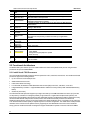
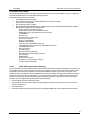
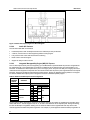
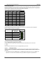
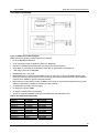
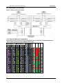
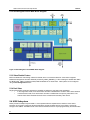
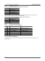
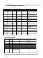
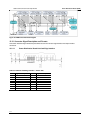
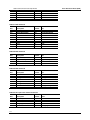
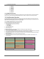
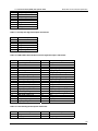
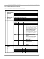
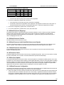
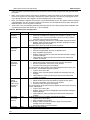
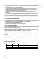
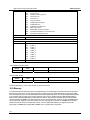
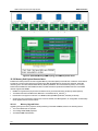
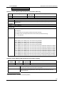
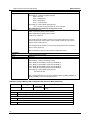
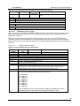
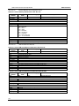
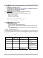
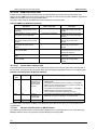
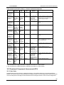
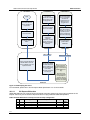
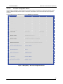
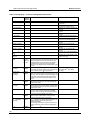
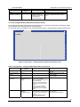
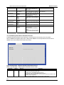
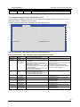
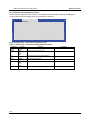
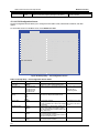
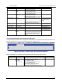
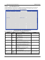
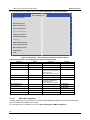
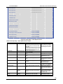
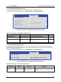
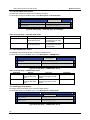
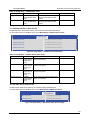
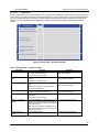
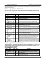
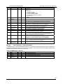
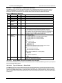
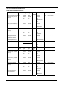
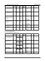
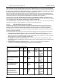
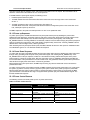
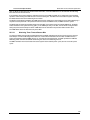
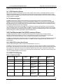
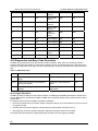
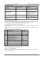
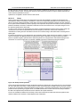
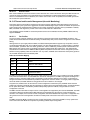
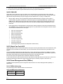
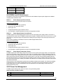
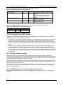
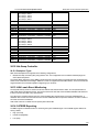
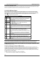
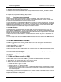
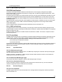
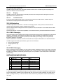
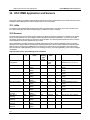
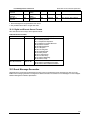
BIOS Initialization
QSSC-S4R Technical Product Specification
Table 90. Formats of Memory RAS Configuration SEL Record for Memory Sparing
Sensor Number Sensor Type Code Event/Reading
Type Code
0x13
0x0C
0x09
Description
Memory RAS Configuration Information for Memory
Sparing
Event Data 1
0x01
Memory Spare RAS Configuration Mode has been activated.
0x00
Memory Spare RAS Configuration Mode has been disabled
Event Data 2
Always 00h
Event Data 3
Always 00h
16.2.12.2.2
IPMI Memory Error Logging
Memory error logging involves the BIOS sending the BMC commands to log memory errors in the system event log
(SEL). The general format of these error formats is described by the Intelligent Platform Management Interface
Specification, Version 2.0.
®
Additionally, the Event Bytes are customized to represent data that is of relevance to the Intel 7500 Chipset
generation of products. The Event/Reading Type field indicates that these SEL entries are described as standard
sensors that have distinct discrete values as described in the Intelligent Platform Management Interface Specification ,
Version 2.0.
16.2.12.2.2.1
Memory ECC Error Records
Table 91. Format of Memory ECC Error SEL Records
Sensor
Number
0x02
Event Data 1
0xA0
0xA1
Event Data 2
Bits [1:0]
Bits [7:2]
Event Data 3
Bits[7:5]
Bits[4:3]
Bits [2:0]
Sensor Type
Code
0x0C
Event/Reading Type
0x6F
Description
Memory ECC error
Correctable ECC error threshold reached
Uncorrectable ECC error
Reserved
When ED1 = 0xA0, Count of Correctable ECC error
When ED1 = 0xA1, Reserved. Set to 0.
®
0-based Identifier or Index into SMBIOS Type16 entry for the system‘s memory array device. For Intel
7500 Chipset server boards and systems that use the Intel® Xeon® 7500 processors, this field
indicates the Memory Board on which the CPU experiencing the memory error sits.
Reserved
Index into SMBIOS Type17 record (memory device) for the failed DDR3 DIMM. This is a 0-based
index that points to the DDR-3 DIMM that has experienced the errors.
Bit[2:0] DIMM Slot#
000b - DIMM_1/B
001b - DIMM_1/A
010b - DIMM_2/B
011b - DIMM_2/A
100b - DIMM_1/D
101b - DIMM_1/C
110b - DIMM_2/D
111b - DIMM_2/C
Note: The DIMM number can be used to decipher the SMI Link and DDR Channel detail.
Bit[0] & Bit[2] together will give DDR Channel. Bit[2] will give SMI Link number.
158