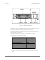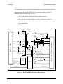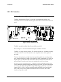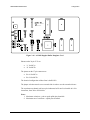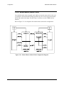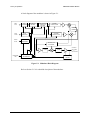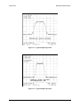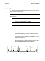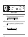
1
SDM-650B Satellite Modem Installation and Operation Manual Part Number MN/SDM650B.IOM Revision 5 EFData Corporation is an ISO 9001 Registered Company SDM-650B Satellite Modem Installation and Operation Manual Part Number MN/SDM650B.IOM Revision 5 May 28, 1996 Special Instructions: This is the sixth edition of the manual. Change bars were not utilized. This revision supersedes part number MN/SDM650 Rev. 4 dated May 5, 1995. Copyright © EFData Corporation, 1995, 1996. All rights reserved. Printed in the USA. EFData Corporation, 2105 West 5th Place, Tempe, Arizona 85281 USA, (602) 968-0447, FAX: (602) 921-9012. Warranty Policy This EFData Corporation product is warranted against defects in material and workmanship for a period of one year from the date of shipment. During the warranty period, EFData will, at its option, repair or replace products that prove to be defective. For equipment under warranty, the customer is responsible for freight to EFData and all related custom, taxes, tariffs, insurance, etc. EFData is responsible for the freight charges only for return of the equipment from the factory to the customer. EFData will return the equipment by the same method (i.e., Air, Express, Surface) as the equipment was sent to EFData. Limitations of Warranty The foregoing warranty shall not apply to defects resulting from improper installation or maintenance, abuse, unauthorized modification, or operation outside of environmental specifications for the product, or, for damages that occur due to improper repackaging of equipment for return to EFData. No other warranty is expressed or implied. EFData Corporation specifically disclaims the implied warranties of merchantability and fitness for particular purpose. Exclusive Remedies The remedies provided herein are the buyer's sole and exclusive remedies. EFData Corporation shall not be liable for any direct, indirect, special, incidental, or consequential damages, whether based on contact, tort, or any other legal theory. Disclaimer EFData has reviewed this manual thoroughly in order that it will be an easy-to-use guide to your equipment. All statements, technical information, and recommendations in this manual and in any guides or related documents are believed reliable, but the accuracy and completeness thereof are not guaranteed or warranted, and they are not intended to be, nor should they be understood to be, representations or warranties concerning the products described. Further, EFData reserves the right to make changes in the specifications of the products described in this manual at any time without notice and without obligation to notify any person of such changes. If you have any questions regarding your equipment or the information in this manual, please contact the EFData Customer Support Department. (For more information, refer to the preface.) Preface About this Manual This manual provides installation and operation information for the EFData SDM-650B satellite modem. This is a technical document intended for earth station engineers, technicians, and operators responsible for the operation and maintenance of the SDM-650B satellite modem. Organization This manual includes the following chapters and appendixes: Rev. 5 • Chapter 1 — describes the unit’s purpose, function, description, options, and system specification. • Chapter 2 — describes the unit’s installation process, external connectors, and system requirements. • Chapter 3 — describes the unit’s configuration. • Chapter 4 — provides front panel operation information. • Chapter 5 — describes the unit’s theory of operation. • Chapter 6 — describes the maintenance of the unit, and provides troubleshooting assistance. • Appendix A — provides data rate change instructions and the differences for fixed and variable rate filters. i Preface SDM-650B Satellite Modem • Appendix B — describes the unit’s remote control operation protocol and command structure. • Appendix C — provides field compatibility specifications. • Appendix D — provides software change instructions. • Appendix E — describes the unit’s Automatic Gain Control (AGC) interface option. • Appendix F — describes the asynchronous overhead channel unit option. • Appendix G — describes the Trojan interface option. • Glossary. Conventions Used in this Manual Cautions and Warnings CAUTION CAUTION indicates a hazardous situation that, if not avoided, may result in minor or moderate injury. CAUTION may also be used to indicate other unsafe practices or risks of property damage. WARNING indicates a potentially hazardous situation that, if not avoided, could result in death or serious injury. WARNING ii Rev. 5 SDM-8000 Satellite Modem Preface References Used in this Manual Military Standards References to “MIL-STD-188” apply to the 114A series (i.e., MIL-STD-188-114A), which provides electrical and functional characteristics of the unbalanced and balanced voltage digital interface circuits applicable to both long haul and tactical communications. Specifically, these references apply to the MIL-STD-188-114A electrical characteristics for a balanced voltage digital interface circuit, Type 1 generator, for the full range of data rates. For more information, refer to the following document: • Department of Defense (DOD) MIL-STD-188-114A, “Electrical Characteristics of Digital Interface Circuits.” Trademarks Product names mentioned in this manual may be trademarks or registered trademarks of their respective companies and are hereby acknowledged. Related Documents The following documents are referenced in this manual: • • • • • • • • Rev. 5 EFData Specification SP/1100 CCITT Recommendation V.35 CCITT Volume III Red Book INTELSAT Document 308 INTELSAT Document 309 Bell System Publication 62411 AT&T Publication 62411 EFData ASYNC Breakout Panel Installation and Operation Manual iii Preface SDM-650B Satellite Modem European EMC Directive In order to meet the European Electro-Magnetic Compatibility (EMC) Directive (EN55022, EN50082-1), properly shielded cables for DATA I/O are required. More specifically, these cables must be double-shielded from end-to-end, ensuring a continuous ground shield. The following information is applicable for the European Low Voltage Directive (EN60950): <HAR> ! Type of power cord required for use in the European Community. CAUTION: Double-pole/Neutral Fusing ACHTUNG: Zweipolige bzw. Neutralleiter-Sicherung International Symbols: Alternating Current. Fuse. Safety Ground. Chassis Ground. Note: For additional symbols, refer to “Cautions and Warnings” listed earlier in this preface. Reporting Comments or Suggestions Concerning this Manual Comments and suggestions regarding the content and design of this manual will be appreciated. To submit comments, please contact the EFData Customer Support Department according to the following information. iv Rev. 5 SDM-8000 Satellite Modem Preface Customer Support Contact the EFData Customer Support Department for: • • • • • Product support Information on returning a product Information on upgrading a product Product training Reporting comments or suggestions concerning manuals An EFData Customer Support representative may be reached at: EFData Corporation Attention: Customer Support Department 2105 West 5th Place Tempe, Arizona 85281 USA (602) 968-0447 (Main EFData Number) (602) 517-2444 (Customer Support Desk) (602) 921-9012 FAX or, E-Mail can be sent to the Customer Support Department at: [email protected] To return an EFData product (in-warranty and out-of-warranty) for repair or replacement: 1. Request a Return Material Authorization (RMA) number from the EFData Customer Support Department. Be prepared to supply the Customer Support representative with the model number, serial number, and a description of the problem. 2. To ensure that the product is not damaged during shipping, pack the product in its original shipping carton/packaging. 3. Ship the product back to EFData. (Shipping charges should be prepaid.) For more information regarding the warranty policies, refer to the disclaimer page located behind the title page. Rev. 5 v Preface SDM-650B Satellite Modem This page is intentionally left blank. vi Rev. 5 Table of Contents CHAPTER 1. INTRODUCTION.................................................................................. 1–1 1.1 Purpose and Function ..................................................................................................................................1–2 1.2 Description ....................................................................................................................................................1–3 1.3 System Specification.....................................................................................................................................1–5 CHAPTER 2. INSTALLATION................................................................................... 2–1 2.1 Unpacking .....................................................................................................................................................2–1 2.2 External Connections...................................................................................................................................2–2 2.2.1 DATA I/O...............................................................................................................................................2–3 2.2.2 Remote (J6).............................................................................................................................................2–3 2.2.3 Fault (J7).................................................................................................................................................2–3 2.2.4 IF Output (CP1) ......................................................................................................................................2–4 2.2.5 IF Input (CP2).........................................................................................................................................2–4 2.2.6 AC Power ...............................................................................................................................................2–4 2.2.7 GROUND ...............................................................................................................................................2–5 2.3 System Requirements...................................................................................................................................2–5 2.4 System Installation .......................................................................................................................................2–6 CHAPTER 3. CONFIGURATION............................................................................... 3–1 3.1 Monitor and Control....................................................................................................................................3–1 3.1.1 Description of Options............................................................................................................................3–2 3.1.1.1 Remote Interface .............................................................................................................................3–2 3.1.1.2 Remote Baud Rate...........................................................................................................................3–3 3.1.1.3 Remote Address ..............................................................................................................................3–4 3.1.1.4 Battery .............................................................................................................................................3–4 3.1.1.5 Modulator/Coder Defaults...............................................................................................................3–5 3.1.1.6 Demodulator/Decoder Defaults.......................................................................................................3–5 Rev. 5 vii Table of Contents SDM-650B Satellite Modem 3.1.1.7 Utility Defaults ................................................................................................................................3–5 3.1.2 Remote Interface Specification...............................................................................................................3–6 3.1.3 M&C Theory of Operation .....................................................................................................................3–6 3.2 Digital Interfaces ..........................................................................................................................................3–7 3.2.1 RS-422 and MIL-STD-188-114 Interface ..............................................................................................3–7 3.2.1.1 Functional Description ....................................................................................................................3–7 3.2.1.2 Connector Pinouts .........................................................................................................................3–12 3.2.1.3 Specification..................................................................................................................................3–13 3.2.2 V.35 Interface .......................................................................................................................................3–14 3.2.2.1 Functional Description ..................................................................................................................3–14 3.2.2.2 Connector Pinouts .........................................................................................................................3–18 3.2.2.3 Specification..................................................................................................................................3–19 3.2.3 DS-1 Interface.......................................................................................................................................3–20 3.2.3.1 Functional Description ..................................................................................................................3–20 3.2.3.2 Connector Pinouts .........................................................................................................................3–23 3.2.3.3 Specification..................................................................................................................................3–23 3.2.4 G.703, 2048 kbit/s Interface .................................................................................................................3–24 3.2.4.1 Functional Description ..................................................................................................................3–24 3.2.4.2 Optional EXT CLK .......................................................................................................................3–26 3.2.4.3 Switch Configuration for G.703 2048 kbit/s Interface ..................................................................3–27 3.2.4.4 Connector Pinouts .........................................................................................................................3–27 3.2.4.5 G.703 2048 kbit/s Connector Board Option..................................................................................3–28 3.2.4.6 External Reference (J3) .................................................................................................................3–30 3.2.4.7 Send Data (J4) ...............................................................................................................................3–30 3.2.4.8 Receive Data (J5) ..........................................................................................................................3–30 3.2.4.9 Specification..................................................................................................................................3–31 3.2.5 Asynchronous Overhead Interface........................................................................................................3–31 3.2.5.1 Functional Description ..................................................................................................................3–31 3.2.5.2 Terrestrial Interface .......................................................................................................................3–32 3.2.5.3 Multiplexer ....................................................................................................................................3–35 3.2.5.4 Demultiplexer ................................................................................................................................3–35 3.2.5.5 Plesiochronous Buffer ...................................................................................................................3–36 3.2.5.6 Remote Interface Specification .....................................................................................................3–36 3.2.5.7 Interface Connector Pinouts ..........................................................................................................3–37 3.2.5.8 Asynchronous Interface Specifications .........................................................................................3–38 3.2.6 Asynchronous Breakout Panel..............................................................................................................3–39 3.3 Doppler Buffer............................................................................................................................................3–40 3.3.1 Buffer Setup..........................................................................................................................................3–44 3.3.1.1 Buffer Size.....................................................................................................................................3–46 3.3.1.2 Doppler..........................................................................................................................................3–46 3.3.1.3 Plesiochronous ..............................................................................................................................3–47 3.3.1.4 Frame/Multiframe Length .............................................................................................................3–47 3.3.1.5 Total Buffer Length.......................................................................................................................3–48 3.3.1.6 Converting .....................................................................................................................................3–48 3.4 Doppler Buffer Specification.....................................................................................................................3–49 3.5 I/O Connectors ...........................................................................................................................................3–49 3.6 Interface Clocking Options .......................................................................................................................3–50 3.6.1 Master/Slave .........................................................................................................................................3–50 3.6.1.1 Master/Slave RS-422 or V.35 .......................................................................................................3–51 viii Rev. 5 SDM-650B Satellite Modem Table of Contents 3.6.1.1.1 Modem Settings (Master).......................................................................................................3–52 3.6.1.1.2 Modem Settings (Slave).........................................................................................................3–52 3.6.1.2 Master/Slave G.703 .......................................................................................................................3–53 3.6.1.3 Master/Slave X.21 .........................................................................................................................3–54 3.6.1.3.1 Modem Settings (Master).......................................................................................................3–54 3.6.1.3.2 Modem Settings (Slave).........................................................................................................3–54 3.6.1.4 Master/Slave External Station Clock.............................................................................................3–55 3.6.1.4.1 Modem Settings (Master).......................................................................................................3–55 3.6.1.4.2 Modem Settings (Slave).........................................................................................................3–55 3.6.2 Master/Master .......................................................................................................................................3–56 3.6.2.1 Master/Master (Customer Clock) ..................................................................................................3–56 3.6.2.1.1 Modem Settings (Master).......................................................................................................3–57 3.6.2.2 Master/Master (Station Clock) ......................................................................................................3–58 3.6.2.2.1 Modem Settings (Master).......................................................................................................3–59 CHAPTER 4. OPERATION........................................................................................ 4–1 4.1 Front Panel ...................................................................................................................................................4–2 4.1.1 LED Indicators........................................................................................................................................4–3 4.1.2 Controls ..................................................................................................................................................4–3 4.1.3 Menus and Options Overview ................................................................................................................4–4 4.1.4 Menu Explanations .................................................................................................................................4–9 4.1.4.1 Select Configuration........................................................................................................................4–9 4.1.4.2 Select Monitor ...............................................................................................................................4–15 4.1.4.3 Select Faults ..................................................................................................................................4–16 4.1.4.3.1 Modulator Faults (Mod_Flts).................................................................................................4–17 4.1.4.3.2 Demodulator/Decoder Faults (Dmd_Flts)..............................................................................4–17 4.1.4.3.3 Common Equipment Faults (CEq_Flts) .................................................................................4–17 4.1.4.4 Select Stored Faults (StFaults) ......................................................................................................4–18 4.1.4.5 Select Utility..................................................................................................................................4–19 CHAPTER 5. THEORY OF OPERATION.................................................................. 5–1 5.1 Modulator .....................................................................................................................................................5–1 5.1.1 Specifications..........................................................................................................................................5–3 5.1.2 Theory of Operation ...............................................................................................................................5–5 5.2 Sequential Decoder/Demodulator Processor .............................................................................................5–7 5.2.1 Specification ...........................................................................................................................................5–8 5.2.2 Theory of Operation ...............................................................................................................................5–9 5.2.2.1 Demodulator Processor ...................................................................................................................5–9 5.2.2.2 Sequential Decoder........................................................................................................................5–10 5.2.2.2.1 Sequential Decoder BER Performance Specifications...........................................................5–12 5.3 Demodulator ...............................................................................................................................................5–16 5.3.1 Specifications........................................................................................................................................5–17 5.3.2 Theory of Operation .............................................................................................................................5–17 5.4 Reacquisition, Fast Acquisition, and Directed Sweep.............................................................................5–18 5.4.1 Reacquisition ........................................................................................................................................5–18 5.4.2 Fast Acquisition ....................................................................................................................................5–19 5.4.3 Directed Sweep.....................................................................................................................................5–20 Rev. 5 ix Table of Contents SDM-650B Satellite Modem CHAPTER 6. MAINTENANCE................................................................................... 6–1 6.1 System Checkout ..........................................................................................................................................6–1 6.1.1 Modulator ...............................................................................................................................................6–1 6.1.2 Demodulator ...........................................................................................................................................6–2 6.1.3 Test Points ..............................................................................................................................................6–8 6.1.3.1 Modulator ........................................................................................................................................6–8 6.1.3.2 Demodulator....................................................................................................................................6–9 6.1.3.3 Sequential Decoder/Demod Card ..................................................................................................6–10 6.2 Fault Isolation.............................................................................................................................................6–11 6.2.1 Modulator Faults (Mod_Flts Menu) .....................................................................................................6–11 6.2.2 Demodulator/Decoder Faults (Dmd_Flts Menu) ..................................................................................6–12 6.2.3 Common Equipment Faults (CEq_Flts Menu) .....................................................................................6–14 6.3 Interface Fault Isolation ............................................................................................................................6–15 6.3.1 Transmit Faults (TX_INTF) .................................................................................................................6–15 6.3.2 Receive Faults (RX_INTF)...................................................................................................................6–16 6.4 Module Replacement .................................................................................................................................6–21 6.5 Module Identification.................................................................................................................................6–21 APPENDIX A. DATA RATES AND FILTERS............................................................A–1 A.1 Fixed Rate Filters ....................................................................................................................................... A–1 A.1.1 Data Rate Change Instructions.............................................................................................................. A–1 A.1.2 Hardware Configuration ....................................................................................................................... A–5 A.2 Variable Rate Filters.................................................................................................................................. A–6 A.2.1 Data Rate Change Instructions.............................................................................................................. A–6 A.2.2 Hardware Configuration ....................................................................................................................... A–7 A.2.3 Utility .................................................................................................................................................... A–9 APPENDIX B. REMOTE CONTROL OPERATION ...................................................B–1 B.1 Standard Version........................................................................................................................................ B–1 B.1.1 General .................................................................................................................................................. B–2 B.1.2 Message Structure ................................................................................................................................. B–2 B.1.2.1 Start Character ............................................................................................................................... B–2 B.1.2.2 Device Address.............................................................................................................................. B–3 B.1.2.3 Command/Response ...................................................................................................................... B–4 B.1.2.4 End Character ................................................................................................................................ B–4 B.1.3 Configuration Commands/Responses ................................................................................................... B–5 B.1.3.1 Set Modulator Frequency............................................................................................................... B–5 B.1.3.2 Set RF Output ................................................................................................................................ B–5 B.1.3.3 Set Demodulator Frequency .......................................................................................................... B–5 B.1.3.4 Set Modulator Power Offset .......................................................................................................... B–6 B.1.3.5 Set Modulator Output Power Level ............................................................................................... B–6 B.1.3.6 Modulator Rate .............................................................................................................................. B–7 B.1.3.6.1 Modulator Filter Rate Assignment ......................................................................................... B–7 B.1.3.6.2 Select Modulator Rate ............................................................................................................ B–8 x Rev. 5 SDM-650B Satellite Modem Table of Contents B.1.3.6.3 Select Modulator Rate Variable ............................................................................................. B–8 B.1.3.7 Demodulator Rate .......................................................................................................................... B–9 B.1.3.7.1 Demodulator Filter Rate Assignment ..................................................................................... B–9 B.1.3.7.2 Select Demodulator Rate ...................................................................................................... B–10 B.1.3.7.3 Select Demodulator Rate Variable ....................................................................................... B–10 B.1.3.8 Scrambler Enable......................................................................................................................... B–10 B.1.3.9 Descrambler Enable..................................................................................................................... B–10 B.1.3.10 Differential Encoder Enable ...................................................................................................... B–11 B.1.3.11 Transmit Clock .......................................................................................................................... B–11 B.1.3.12 Receive Clock ............................................................................................................................ B–11 B.1.3.13 Baseband Loopback................................................................................................................... B–11 B.1.3.14 RF Loopback ............................................................................................................................. B–12 B.1.3.15 IF Loopback............................................................................................................................... B–12 B.1.3.16 Time of Day............................................................................................................................... B–12 B.1.3.17 Date............................................................................................................................................ B–13 B.1.3.18 Remote....................................................................................................................................... B–13 B.1.3.19 Clear Stored Faults .................................................................................................................... B–13 B.1.3.20 BER Threshold .......................................................................................................................... B–13 B.1.3.21 Sweep Reacquisition.................................................................................................................. B–14 B.1.3.22 Fast Acquisition Mode............................................................................................................... B–14 B.1.3.22.1 Sweep Center Frequency.................................................................................................... B–15 B.1.3.22.2 Sweep Width Range ........................................................................................................... B–15 B.1.3.22.3 Sweep Direction ................................................................................................................. B–16 B.1.3.23 Modem Operation Mode............................................................................................................ B–16 B.1.3.24 Buffer Control Mode ................................................................................................................. B–16 B.1.3.24.1 Buffer Clock ....................................................................................................................... B–17 B.1.3.24.2 Interface Buffer Center....................................................................................................... B–17 B.1.3.24.3 Interface Buffer Size .......................................................................................................... B–17 B.1.4. Status Commands/Responses............................................................................................................. B–18 B.1.4.1 Configuration............................................................................................................................... B–18 B.1.4.1.1 Modulator/Coder Status ....................................................................................................... B–18 B.1.4.1.2 Modulator/Coder Program.................................................................................................... B–18 B.1.4.1.3 Demodulator/Decoder Configuration Status ........................................................................ B–19 B.1.4.1.4 Demodulator/Decoder Configuration Program .................................................................... B–20 B.1.4.2 Modem Faults Status (Summary) ................................................................................................ B–20 B.1.4.3 Modulator Status.......................................................................................................................... B–21 B.1.4.4 Demodulator Status...................................................................................................................... B–21 B.1.4.5 Common Equipment Status ......................................................................................................... B–22 B.1.4.6 Interface Receive Side Status ...................................................................................................... B–22 B.1.4.7 BER Status................................................................................................................................... B–23 B.1.4.7.1 Raw BER.............................................................................................................................. B–23 B.1.4.7.2 Corrected BER ..................................................................................................................... B–23 B.1.4.8 Eb/N0 Status.................................................................................................................................. B–24 B.1.4.9 Modulator Rate Status ................................................................................................................. B–24 B.1.4.10 Demodulator Rate Status ........................................................................................................... B–24 B.1.4.11 Receive Signal Level Status ...................................................................................................... B–25 B.1.4.12 Current Sweep Value ................................................................................................................. B–25 B.1.4.13 Stored Faults .............................................................................................................................. B–26 B.1.4.13.1 Modulator Stored Faults ..................................................................................................... B–26 B.1.4.13.2 Demodulator Stored Faults................................................................................................. B–26 B.1.4.13.3 Common Equipment Stored Faults..................................................................................... B–27 B.1.4.13.4 Interface Receive Side Status Stored Faults ....................................................................... B–27 B.1.4.14 Bulk Consolidated Status........................................................................................................... B–28 B.1.4.15 Bulk Consolidated Analog Status .............................................................................................. B–30 Rev. 5 xi Table of Contents SDM-650B Satellite Modem B.1.4.16 Bulk Consolidated Status Faults ................................................................................................ B–30 B.1.4.17 Change Status ............................................................................................................................ B–31 B.1.4.18 Equipment Type......................................................................................................................... B–32 B.2 Asynchronous Overhead Interface Support Option ............................................................................. B–33 B.2.1 General ................................................................................................................................................ B–33 B.2.2 Message Structure ............................................................................................................................... B–33 B.2.2.1 Start Character ............................................................................................................................. B–34 B.2.2.2 Device Address............................................................................................................................ B–34 B.2.2.3 Command/Response .................................................................................................................... B–35 B.2.2.4 End Character .............................................................................................................................. B–35 B.2.3 Modulator Configuration Commands ................................................................................................. B–36 B.2.3.1 Set Modulator Frequency............................................................................................................. B–36 B.2.3.2 Set RF Output .............................................................................................................................. B–36 B.2.3.3 Set Modulator Power Offset ........................................................................................................ B–36 B.2.3.4 Set Modulator Output Power Level ............................................................................................. B–37 B.2.3.5 Modulator Rate ............................................................................................................................ B–38 B.2.3.5.1 Modulator Filter Rate Assignment ....................................................................................... B–38 B.2.3.5.2 Select Modulator Rate .......................................................................................................... B–39 B.2.3.5.3 Select Modulator Rate Variable ........................................................................................... B–39 B.2.3.6 Scrambler Enable......................................................................................................................... B–39 B.2.3.7 Differential Encoder Enable ........................................................................................................ B–40 B.2.4 Demodulator Configuration Commands ............................................................................................. B–40 B.2.4.1 Set Demodulator Frequency ........................................................................................................ B–40 B.2.4.2 Demodulator Rate ........................................................................................................................ B–40 B.2.4.2.1 Demodulator Filter Rate Assignment ................................................................................... B–41 B.2.4.2.2 Select Demodulator Rate ...................................................................................................... B–41 B.2.4.2.3 Select Demodulator Rate Variable ....................................................................................... B–41 B.2.4.3 Descramble Enable ...................................................................................................................... B–42 B.2.4.4 RF Loopback ............................................................................................................................... B–42 B.2.4.5 IF Loopback................................................................................................................................. B–42 B.2.4.6 BER Threshold ............................................................................................................................ B–42 B.2.4.7 Sweep Reacquisition.................................................................................................................... B–43 B.2.4.8 Fast Acquisition Mode................................................................................................................. B–43 B.2.4.8.1 Sweep Center Frequency...................................................................................................... B–44 B.2.4.8.2 Sweep Width Range ............................................................................................................. B–44 B.2.4.8.3 Sweep Direction ................................................................................................................... B–45 B.2.5 Interface Configuration Commands .................................................................................................... B–45 B.2.5.1 Transmit Clock ............................................................................................................................ B–45 B.2.5.2 Buffer Clock ................................................................................................................................ B–45 B.2.5.3 Receive Clock .............................................................................................................................. B–46 B.2.5.4 External Reference Frequency..................................................................................................... B–46 B.2.5.5 Interface Loopback ...................................................................................................................... B–46 B.2.5.6 Baseband Loopback..................................................................................................................... B–46 B.2.5.7 Interface Coding Format Transmit............................................................................................... B–47 B.2.5.8 Interface Coding Format Receive ................................................................................................ B–47 B.2.5.9 Interface Buffer Center ................................................................................................................ B–47 B.2.5.10 Interface Buffer Size.................................................................................................................. B–47 B.2.5.11 Transmit Overhead Baud Rate................................................................................................... B–48 B.2.5.12 Receive Overhead Baud Rate .................................................................................................... B–48 B.2.5.13 Overhead Channels Character Length ....................................................................................... B–48 B.2.5.14 Overhead Channels Stop Bits .................................................................................................... B–48 B.2.5.15 Overhead Channels Parity ......................................................................................................... B–49 B.2.5.16 Interface Substitution Pattern (Transmit 2047 Pattern) ............................................................. B–49 xii Rev. 5 SDM-650B Satellite Modem Table of Contents B.2.6 System Commands/Responses ............................................................................................................ B–49 B.2.6.1 Time of Day................................................................................................................................. B–49 B.2.6.2 Date.............................................................................................................................................. B–50 B.2.6.3 Remote......................................................................................................................................... B–50 B.2.6.4 Clear Stored Faults ...................................................................................................................... B–50 B.2.6.5 Modem Operation Mode.............................................................................................................. B–51 B.2.7 Automatic Uplink Power Control (AUPC) Configuration Commands............................................... B–51 B.2.7.1 Local Modem AUPC Commands ................................................................................................ B–51 B.2.7.1.1 Local AUPC Enable ............................................................................................................. B–51 B.2.7.1.2 Nominal AUPC Power Level ............................................................................................... B–51 B.2.7.1.3 Maximum AUPC Power Limit............................................................................................. B–52 B.2.7.1.4 Minimum AUPC Power Limit ............................................................................................. B–52 B.2.7.1.5 Eb/N0 Target AUPC Set Point............................................................................................... B–52 B.2.7.1.6 Maximum AUPC Tracking Rate .......................................................................................... B–52 B.2.7.1.7 AUPC Local Carrier Loss Action......................................................................................... B–53 B.2.7.1.8 AUPC Remote Carrier Loss Action ..................................................................................... B–53 B.2.7.2 Remote Modem AUPC Commands............................................................................................. B–53 B.2.7.2.1 Remote AUPC Enable.......................................................................................................... B–53 B.2.7.2.2 Remote Interface Substitution Pattern (Transmit 2047 Pattern)........................................... B–54 B.2.7.2.3 Remote Interface Baseband Loopback ................................................................................. B–54 B.2.7.2.4 Remote Interface Read Error Status (Received 2047 Pattern) ............................................. B–54 B.2.8 Status Commands/Responses.............................................................................................................. B–55 B.2.8.1 Configuration Status .................................................................................................................... B–55 B.2.8.1.1 Modulator/Coder Configuration Status ................................................................................ B–55 B.2.8.1.2 Modulator/Coder Configuration Program ............................................................................ B–56 B.2.8.1.3 Demodulator/Decoder Configuration Status ........................................................................ B–57 B.2.8.1.4 Demodulator/Decoder Configuration Program .................................................................... B–58 B.2.8.1.5 Interface Configuration Status.............................................................................................. B–59 B.2.8.1.6 AUPC Configuration Status ................................................................................................. B–59 B.2.8.2 Modem Faults Status (Summary) ................................................................................................ B–60 B.2.8.3 Modulator Status.......................................................................................................................... B–60 B.2.8.4 Demodulator Status...................................................................................................................... B–60 B.2.8.5 Common Equipment Status ......................................................................................................... B–61 B.2.8.6 Interface Transmit Side Status ..................................................................................................... B–61 B.2.8.7 Interface Receive Side Status ...................................................................................................... B–61 B.2.8.8 Bit Error Rate Status .................................................................................................................... B–62 B.2.8.8.1 Raw BER.............................................................................................................................. B–62 B.2.8.8.2 Corrected BER ..................................................................................................................... B–62 B.2.8.9 Eb/N0 ............................................................................................................................................ B–63 B.2.8.10 Modulator Rate .......................................................................................................................... B–63 B.2.8.11 Demodulator Rate ...................................................................................................................... B–63 B.2.8.12 Receive Signal Level ................................................................................................................. B–64 B.2.8.13 Current Sweep Value ................................................................................................................. B–64 B.2.8.14 Interface Buffer Fill Status ........................................................................................................ B–64 B.2.8.15 Interface Read Error Status........................................................................................................ B–64 B.2.8.16 Stored Faults .............................................................................................................................. B–65 B.2.8.16.1 Modulator Stored Faults ..................................................................................................... B–65 B.2.8.16.2 Demodulator Stored Faults................................................................................................. B–65 B.2.8.16.3 Common Equipment Stored Faults..................................................................................... B–66 B.2.8.16.4 Interface Transmit Side Stored Faults ................................................................................ B–66 B.2.8.16.5 Interface Receive Side Stored Faults.................................................................................. B–66 B.2.8.17 Bulk Consolidated Status........................................................................................................... B–67 B.2.8.18 Bulk Consolidated Analog Status .............................................................................................. B–69 B.2.8.19 Bulk Consolidated Status Faults ................................................................................................ B–70 Rev. 5 xiii Table of Contents SDM-650B Satellite Modem B.2.8.20 Change Status ............................................................................................................................ B–72 B.2.8.21 Equipment Type......................................................................................................................... B–72 B.2.8.22 Bulk Consolidated Status AUPC ............................................................................................... B–72 APPENDIX C. FIELD COMPATIBILITY ....................................................................C–1 C.1 SDM-650B Standard Modem.................................................................................................................... C–1 C.2 SDM-650B Fairchild-Compatible Modem ............................................................................................... C–2 C.3 SDM-650B Aydin Data Rate Modem ....................................................................................................... C–2 C.4 SDM-650B Comstream Modem ................................................................................................................ C–2 APPENDIX D. SOFTWARE CHANGE INSTRUCTIONS...........................................D–1 APPENDIX E. AGC INTERFACE ..............................................................................E–1 E.1 Connector Pinouts ...................................................................................................................................... E–2 E.2 Installation Instructions............................................................................................................................. E–2 E.2.1 Parts Required ....................................................................................................................................... E–2 E.2.2 Installation Procedure............................................................................................................................ E–3 APPENDIX F. ASYNCHRONOUS OVERHEAD CHANNEL UNIT ............................ F–1 F.1 Functional Description of ASYNC Overhead Channel Unit .................................................................. F–2 F.1.1 Terrestrial Interface ................................................................................................................................F–4 F.1.2 Multiplexer .............................................................................................................................................F–6 F.1.3 Demultiplexer .........................................................................................................................................F–6 F.1.4 Plesiochronous Buffer ............................................................................................................................F–7 F.2 ASYNC Interface Connector Pinouts ....................................................................................................... F–8 F.3 ASYNC Interface Specifications................................................................................................................ F–9 F.4 Functional Description of ASYNC Overhead Channel Unit with AUPC............................................ F–10 F.4.1 AUPC ...................................................................................................................................................F–10 F.4.2 Modem-to-Modem Channel for Remote M&C ....................................................................................F–11 F.5 Front Panel Operation ............................................................................................................................. F–12 F.5.1 Menus and Options Overview ..............................................................................................................F–13 F.5.2 Menu Explanations ...............................................................................................................................F–20 F.5.2.1 Select Configuration......................................................................................................................F–20 F.5.2.1.1 Configuration Modulator .......................................................................................................F–21 F.5.2.1.2 Configuration Demodulator ...................................................................................................F–23 F.5.2.1.3 Configuration Interface..........................................................................................................F–25 F.5.2.1.4 Configuration AUPC .............................................................................................................F–28 F.5.2.2 Select Monitor...............................................................................................................................F–29 F.5.2.3 Select Faults ..................................................................................................................................F–30 xiv Rev. 5 SDM-650B Satellite Modem Table of Contents F.5.2.3.1 Modulator Faults (Mod_FLTS) .............................................................................................F–31 F.5.2.3.2 Demodulator/Decoder Faults (Dmd_Flts) .............................................................................F–31 F.5.2.3.3 Common Equipment Faults (CEq_Flts).................................................................................F–31 F.5.2.3.4 Transmit Faults (TX_INTF) ..................................................................................................F–32 F.5.2.3.5 Receive Faults (RX_INTF)....................................................................................................F–32 F.5.2.4 Select Stored Faults (StFaults) ......................................................................................................F–33 F.5.2.5 Select Remote................................................................................................................................F–34 F.5.2.5.1 Remote Configuration............................................................................................................F–34 F.5.2.5.2 Remote Monitor .....................................................................................................................F–34 F.5.2.6 Select Utility..................................................................................................................................F–35 APPENDIX G. TROJAN INTERFACE ...................................................................... G–1 G.1 Functional Description ..............................................................................................................................G–1 G.2 Connector Pinouts......................................................................................................................................G–5 G.3 Specification................................................................................................................................................G–6 G.3.1 MIL-STD-188-114 Parameters............................................................................................................. G–6 G.3.2 Clock Synthesizer/Dejitter Circuit ........................................................................................................ G–6 G.3.3 Doppler Buffer Parameters ................................................................................................................... G–6 G.4 Configuration Guide ..................................................................................................................................G–7 G.4.1 Modulator/Coder Defaults .................................................................................................................... G–7 G.4.2 Demodulator/Decoder Defaults (Dmd_Flts)......................................................................................... G–8 G.4.3 Interface Defaults.................................................................................................................................. G–8 G.5 Front Panel Operation...............................................................................................................................G–9 G.5.1 Menus and Options Overview .............................................................................................................. G–9 G.5.2 Menu Explanations ............................................................................................................................. G–14 G.5.2.1 Select Configuration .................................................................................................................... G–14 G.5.2.2 Select Monitor ............................................................................................................................. G–14 G.5.2.3 Select Faults................................................................................................................................. G–14 G.5.2.3.1 Modulator Faults (Mod_Flts) ............................................................................................... G–14 G.5.2.3.2 Demodulator/Decoder Faults (Dmd_Flts)............................................................................ G–14 G.5.2.3.3 Common Equipment Faults (CEq_Flts) ............................................................................... G–14 G.5.2.4 Select Stored Faults (StFaults) .................................................................................................... G–15 G.5.2.5 Select Utility ................................................................................................................................ G–15 G.6 Remote Control Operation......................................................................................................................G–16 G.6.1 General................................................................................................................................................ G–16 G.6.1.1 Message Structure........................................................................................................................ G–16 G.6.1.1.1 Start Character ...................................................................................................................... G–17 G.6.1.1.2 Device Address .................................................................................................................... G–17 G.6.2 Command/Response............................................................................................................................ G–18 G.6.3 End Character ..................................................................................................................................... G–18 G.6.4 Configuration Commands/Responses ................................................................................................. G–19 G.6.4.1 Modulator .................................................................................................................................... G–19 G.6.4.1.1 Set Modulator Frequency ..................................................................................................... G–19 G.6.4.1.2 Set RF Output....................................................................................................................... G–19 G.6.4.1.3 Modulator Rate..................................................................................................................... G–20 G.6.4.1.3.1 Modulator Filter Rate Assignment................................................................................ G–20 G.6.4.1.3.2 Select Modulator Rate................................................................................................... G–21 Rev. 5 xv Table of Contents SDM-650B Satellite Modem G.6.4.1.3.3 Select Modulator Rate Variable.................................................................................... G–21 G.6.4.1.3.4 Set Modulator Power Offset ......................................................................................... G–21 G.6.4.1.3.5 Set Modulator Output Power Level .............................................................................. G–22 G.6.4.1.3.6 Scrambler Enable .......................................................................................................... G–22 G.6.4.1.3.7 Differential Encoder Enable ......................................................................................... G–22 G.6.4.2 Demodulator ................................................................................................................................ G–23 G.6.4.2.1 Set Demodulator Frequency................................................................................................. G–23 G.6.4.2.2 Demodulator Rate ................................................................................................................ G–23 G.6.4.2.2.1 Demodulator Filter Rate Assignment ........................................................................... G–24 G.6.4.2.2.2 Select Demodulator Rate .............................................................................................. G–24 G.6.4.2.2.3 Select Demodulator Rate Variable................................................................................ G–24 G.6.4.2.3 Descramble Enable............................................................................................................... G–25 G.6.4.2.4 IF Loopback ......................................................................................................................... G–25 G.6.4.2.5 RF Loopback........................................................................................................................ G–25 G.6.4.2.6 Sweep Reacquisition ............................................................................................................ G–25 G.6.4.2.7 Fast Acquisition Mode ......................................................................................................... G–26 G.6.4.2.8 Sweep Center Frequency...................................................................................................... G–26 G.6.4.2.9 Sweep Width Range............................................................................................................. G–27 G.6.4.2.10 Sweep Direction ................................................................................................................. G–27 G.6.4.2.11 Bit Error Rate Threshold .................................................................................................... G–27 G.6.4.3 Interface/Doppler Buffer ............................................................................................................. G–28 G.6.4.3.1 Baseband Loopback ............................................................................................................. G–28 G.6.4.3.2 Transmit Clock..................................................................................................................... G–28 G.6.4.3.3 Receive Clock ...................................................................................................................... G–28 G.6.4.3.4 External Reference Frequency ............................................................................................. G–28 G.6.4.3.5 Interface Reference Clock.................................................................................................... G–29 G.6.4.3.6 Interface Buffer Center ........................................................................................................ G–29 G.6.4.3.7 Interface Buffer Depth ......................................................................................................... G–29 G.6.4.4 System Commands/Responses .................................................................................................... G–30 G.6.4.4.1 Time of Day ......................................................................................................................... G–30 G.6.4.4.2 Date ...................................................................................................................................... G–30 G.6.4.4.3 Remote ................................................................................................................................. G–31 G.6.4.4.4 Clear Stored Faults............................................................................................................... G–31 G.6.4.4.5 Modem Operation Mode ...................................................................................................... G–31 G.6.4.5 Status Commands/Responses ...................................................................................................... G–32 G.6.4.5.1 Configuration ....................................................................................................................... G–32 G.6.4.5.1.1 Modulator/Coder Configuration Status......................................................................... G–32 G.6.4.5.1.2 Modulator/Coder Configuration Program..................................................................... G–33 G.6.4.5.1.3 Demodulator/Decoder Configuration Status................................................................. G–33 G.6.4.5.1.4 Demodulator/Decoder Configuration Program............................................................. G–34 G.6.4.5.1.5 Interface Configuration Status ...................................................................................... G–34 G.6.4.5.2 Modem Faults Status (Summary)......................................................................................... G–35 G.6.4.5.3 Modulator Status .................................................................................................................. G–35 G.6.4.5.4 Demodulator Status .............................................................................................................. G–35 G.6.4.5.5 Common Equipment Status.................................................................................................. G–36 G.6.4.5.6 Bit Error Rate Status ............................................................................................................ G–36 G.6.4.5.6.1 Raw BER ...................................................................................................................... G–36 G.6.4.5.6.2 Corrected BER.............................................................................................................. G–37 G.6.4.5.7 Eb/N0 ..................................................................................................................................... G–37 G.6.4.5.8 Modulator Rate..................................................................................................................... G–37 G.6.4.5.9 Demodulator Rate ................................................................................................................ G–38 G.6.4.5.10 Receive Signal Level.......................................................................................................... G–38 G.6.4.5.11 Current Sweep Value ......................................................................................................... G–38 G.6.4.5.12 Stored Faults ...................................................................................................................... G–38 xvi Rev. 5 SDM-650B Satellite Modem Table of Contents G.6.4.5.12.1 Modulator Stored Faults ............................................................................................. G–39 G.6.4.5.12.2 Demodulator Stored Faults ......................................................................................... G–39 G.6.4.5.12.3 Common Equipment Stored Faults ............................................................................. G–39 G.6.4.5.13 Bulk Consolidated Status ................................................................................................... G–40 G.6.4.5.14 Bulk Consolidated Analog Status ...................................................................................... G–42 G.6.4.5.15 Bulk Consolidated Status Faults ........................................................................................ G–42 G.6.4.5.16 Change Status..................................................................................................................... G–43 G.6.4.5.17 Equipment Type ................................................................................................................. G–44 GLOSSARY ............................................................................................................... g–1 Rev. 5 xvii Table of Contents SDM-650B Satellite Modem Figures Figure 1-1. SDM-650B....................................................................................................................................1–1 Figure 1-2. Satellite Communications System with an SDM-650B ................................................................1–2 Figure 1-3. Modular Construction ...................................................................................................................1–4 Figure 1-4. Sequential Decoder BER Performance Curves (1/2 Rate)............................................................1–8 Figure 1-5. Sequential Decoder BER Performance Curves (3/4 Rate)............................................................1–9 Figure 1-6. Sequential Decoder BER Performance Curves (7/8 Rate)..........................................................1–10 Figure 1-7. Viterbi Decoder BER Performance Curves (1/2 Rate) ...............................................................1–11 Figure 1-8. SDM-650B Typical Output Spectrum ........................................................................................1–12 Figure 2-1. SDM-650B Rear Panel View ........................................................................................................2–2 Figure 3-1. M&C Card ....................................................................................................................................3–2 Figure 3-2. RS-422 and MIL-STD-188-114 Interface Board..........................................................................3–7 Figure 3-3. RS-422 and MIL-STD-188-114 Block Diagram ..........................................................................3–8 Figure 3-4. V.35 Interface Card.....................................................................................................................3–14 Figure 3-5. V.35 Interface Block Diagram ....................................................................................................3–15 Figure 3-6. DS-1 Interface Card ....................................................................................................................3–20 Figure 3-7. DS-1 Interface Block Diagram....................................................................................................3–21 Figure 3-8. G.703 2048 kbit/s Interface Card................................................................................................3–24 Figure 3-9. G.703 2048 Interface Block Diagram .........................................................................................3–25 Figure 3-10. G.703 2048 kbit/s Interface Connector Board (Optional).........................................................3–28 Figure 3-11. G.703 2048 kbit/s Connector Board Schematic Diagram .........................................................3–29 Figure 3-12. Asynchronous Overhead Interface Block Diagram ..................................................................3–32 Figure 3-13. Asynchronous Overhead Jumpers.............................................................................................3–33 Figure 3-14. AS/3812 Doppler Buffer Daughter Card ..................................................................................3–43 Figure 3-15. Clock Slip Diagram...................................................................................................................3–45 Figure 3-16. RS-422 or V.35 Master Slave Configuration............................................................................3–51 Figure 3-17. G.703 Master Slave Configuration ...........................................................................................3–53 Figure 3-18. X.21 Master/Slave Configuration .............................................................................................3–54 Figure 3-19. G.703 Master Slave Configuration ...........................................................................................3–55 Figure 3-20. Master/Master Customer Clock Configuration .........................................................................3–56 Figure 3-21. Master/Master Station Clock Configuration Diagram ..............................................................3–58 Figure 4-1. SDM-650B Front Panel View.......................................................................................................4–2 Figure 5-1. Modulator Block Diagram ............................................................................................................5–2 Figure 5-2. Modulator Output Spectral Occupancy.........................................................................................5–4 Figure 5-3. Decoder Block Diagram................................................................................................................5–7 Figure 5-4. Sequential Decoder BER Performance Curves (1/2 Rate)..........................................................5–13 Figure 5-5. Sequential Decoder BER Performance Curves (3/4 Rate)..........................................................5–14 Figure 5-6. Sequential Decoder BER Performance Curves (7/8 Rate)..........................................................5–15 Figure 5-7. Demodulator Block Diagram ......................................................................................................5–16 Figure 6-1. Typical Output Spectrum ..............................................................................................................6–4 Figure 6-2. Typical Output Spectrum ..............................................................................................................6–4 Figure 6-3. Typical Eye Pattern with Noise (Approximately 7.5 dB Eb/N0) ...................................................6–6 Figure 6-4. Typical Eye Pattern without Noise ...............................................................................................6–6 Figure 6-5. Typical Eye Constellation with Noise (Approximately 7.5 dB Eb/N0) .........................................6–7 Figure 6-6. Typical Eye Constellation without Noise......................................................................................6–7 Figure 6-7. Modulator Test Points...................................................................................................................6–8 Figure 6-8. Demodulator Test Points...............................................................................................................6–9 Figure 6-9. Sequential Decoder/Demod Card Test Points.............................................................................6–10 Figure 6-10. Rear View Without Cover.........................................................................................................6–20 Figure A-1. Modulator Filter Card Change .................................................................................................... A–2 Figure A-2. Demodulator Filter Card Change ................................................................................................ A–4 xviii Rev. 5 SDM-650B Satellite Modem Figure E-1. Figure E-2. Figure E-3. Figure F-1. Figure F-2. Figure G-1. Rev. 5 Table of Contents Rear Panel View .......................................................................................................................... E–2 Wiring Diagram........................................................................................................................... E–4 AGC Adapter Board .................................................................................................................... E–5 Asynchronous Overhead Interface Block Diagram ......................................................................F–3 Asynchronous Overhead Interface Board.....................................................................................F–5 Trojan Interface Block Diagram ................................................................................................. G–2 xix Table of Contents SDM-650B Satellite Modem Tables Table 1-1. Operating Specifications ................................................................................................................1–5 Table 1-2. BER Performance Specifications ...................................................................................................1–7 Table 2-1. Rear Panel Connectors ...................................................................................................................2–2 Table 3-1. AS/0627-3 Rev. E Board Jumper Selection .................................................................................3–11 Table 3-2. AS/0627-2 Rev. E Board Jumper Selection .................................................................................3–17 Table 3-3. Equalizer Control .........................................................................................................................3–22 Table 3-4. G.703, 2048 kbit/s Interface Switch Configurations ....................................................................3–26 Table 3-5. G.703 2048 kbit/s Interface Connector Jumpers ..........................................................................3–29 Table 3-6. Asynchronous Overhead Jumper Table........................................................................................3–34 Table 3-7. Data Rate Jumper Table ...............................................................................................................3–34 Table 3-8. Jumper Selections.........................................................................................................................3–41 Table 3-9. INTELSAT Delay Variations.......................................................................................................3–41 Table 4-1. Main Front Panel Menu (Standard)................................................................................................4–4 Table 4-2. Select Configuration Menu ............................................................................................................4–5 Table 4-3. Select Monitor Menu......................................................................................................................4–6 Table 4-4. Select Faults Menu .........................................................................................................................4–6 Table 4-5. Select Stored Faults (StFaults) Menu .............................................................................................4–7 Table 4-6. Select Utility Menu.........................................................................................................................4–8 Table 6-1. EFData Conversion of (S+N)/N to S/N and Eb/N0 for Various Code Rates...................................6–5 Table 6-2. Programmable Data Rates for the Variable Rate SDM-650B Modem.........................................6–17 Table 6-3. EFData Part Numbers for SDM-650B Modules...........................................................................6–22 Table D-1. EFData M&C Viterbi Decoder Firmware .................................................................................... D–2 Table F-1. Asynchronous Overhead Jumpers..................................................................................................F–5 Table F-2. Data Rate Jumpers..........................................................................................................................F–5 Table F-3. Main Front Panel Menu with Asynchronous Overhead (with AUPC) ........................................F–13 Table F-4. Select Configuration Modulator Menu (with AUPC) ..................................................................F–13 Table F-5. Select Configuration Demodulator Menu (with AUPC) ..............................................................F–14 Table F-6. Select Configuration Interface Menu (with AUPC).....................................................................F–15 Table F-7. Select Configuration AUPC Menu (with AUPC) ........................................................................F–16 Table F-8. Select Monitor Menu (with AUPC) .............................................................................................F–16 Table F-9. Select Faults Menu (with AUPC).................................................................................................F–17 Table F-10. Select Stored Faults (StFaults) Menu (with AUPC) ..................................................................F–18 Table F-11. Select Remote Menu (with AUPC) ............................................................................................F–18 Table F-12. Select Utility Menu (with AUPC) ..............................................................................................F–19 Table G-1. Main Front Panel Menu (Trojan Interface) .................................................................................. G–9 Table G-2. Select Configuration Modulator Menu....................................................................................... G–10 Table G-3. Select Configuration Demodulator Menu................................................................................... G–10 Table G-4. Select Configuration Interface Menu ......................................................................................... G–11 Table G-5. Select Monitor Menu .................................................................................................................. G–11 Table G-6. Select Faults (StFaults) Menu..................................................................................................... G–12 Table G-7. Select StFaults Menu .................................................................................................................. G–13 Table G-8. Select Utility Menu..................................................................................................................... G–13 xx Rev. 5 Chapter 1. INTRODUCTION This manual describes the SDM-650B satellite modem, referred to in this document as “the modem” (Figure 1-1). Figure 1-1. SDM-650B Rev. 5 1–1 Introduction SDM-650B Satellite Modem 1.1 Purpose and Function The modem is a high performance, full-duplex, Bi-Phase Shift Keying/Quadrature Phase Shift Keying (BPSK/QPSK), digital modulator/demodulator (modem), for Frequency Division Multiple Access (FDMA) satellite communication systems. The modem provides an interface between Single Channel Per Carrier (SCPC) fixed-rate terminal equipment, having a data rate of 19.2 kbit/s to 3.584 Mbit/s. The modem also provides an interface between IF converter equipment operating in a 50 to 90 MHz band, or 100 to 180 MHz band (Figure 1-2). CUSTOMER DATA DIGITAL INTERFACE ENCODER/ MODULATOR TRANSMIT RF EQUIPMENT ANTENNA REMOTE SERIAL INTERFACE MICROCOMPUTER POWER SUPPLY AC POWER FAULT INDICATORS SDM-650B SATELLITE DATA MODEM DEMODULATOR/ DECODER RECEIVE RF EQUIPMENT Figure 1-2. Satellite Communications System with an SDM-650B 1–2 Rev. 5 SDM-650B Satellite Modem Introduction The modem contains: • Built-in scrambler/descrambler • Differential encoder/decoder • Transmit and receive frequency synthesizers • Multi-rate Forward Error Correction (FEC) convolutional encoder-sequential decoder (Viterbi K=7 is optional) The modem provides high performance with: • • • • Narrow occupied bandwidth Automatic signal acquisition High flexibility Extensive online monitoring circuits 1.2 Description The modem is a complete, self-contained unit in a standard 19” rack-mountable enclosure weighing approximately 25 lbs. The modem is of modular construction (Figure 1-3). The chassis assembly (with the front and rear panel) encloses several Printed Circuit Boards (PCBs). The backplane PCB is mounted on the chassis assembly, and contains receptacles for five plug-in PCBs. Rev. 5 1–3 Introduction SDM-650B Satellite Modem Figure 1-3. Modular Construction Test points are located on the front board edge of the modulator, demodulator, and decoder PCBs. Refer to Section 6.1.4 for listings and diagrams of the test points. All controls and indicators for operation of the modem are located on the front panel. For more information, refer to Chapter 4. The chassis also contains the power supply; a fan is located on the rear panel. The modem consists of the following assemblies: Assembly Chassis with Power Supply PCB, M&C PCB, Modulator PCB, Demodulator PCB, Sequential Decoder PCB, Front Panel Control Board PCB, Mother Board PCB, Digital Interface V.35 PCB, Digital Interface DS1 PCB, Digital Interface MIL-STD-188-114 PCB, Doppler Buffer PCB, Asynchronous Overhead Channel Unit Drawing # AS/1099 AS/0356 AS/0773-X AS/0778-X AS/0365-X AS/0361 AS/0979-1 AS/0627-2 (Optional) AS/0569 (Optional) AS/0627-3 (Optional) AS/3812 (Optional) AS/1311-X (Optional) Note: X = various options available on the modulator, demodulator, and decoder boards. 1–4 Rev. 5 SDM-650B Satellite Modem Introduction 1.3 System Specification Table 1-1 lists the operating specifications of the modem. Table 1-1. Operating Specifications System Specifications Operating Frequency Range Type of Modulation Operating Channel Spacing BER Digital Interface Digital Data Rate: Variable Rate Single Rate Forward Error Correction Data Scrambling Diagnostic Features Prime Power Size 50 to 90 MHz, or 100 to 180 MHz. Synthesized in 2.5 kHz steps. QPSK. BPSK. Less than 0.5 dB degradation operating with 2 adjacent like channels each 10 dB higher at 1.3 times the symbol rate or 75 kHz minimum. See Table 1-2. RS-422/-449. V.35. DS-1 STD. G.703. Others optional. 19.2 to 3584 kbit/s configurable. Choice of up to four pre-defined rates, or variable rate option. 19.2 to 48 kbit/s, 1/2 rate BPSK only. 19.2 to 2048 kbit/s. 19.2 to 3584 kbit/s. 2048 kbit/s maximum for 1/2 rate. 3072 kbit/s maximum for 3/4 rate. 3584 kbit/s maximum for 7/8 rate. Convolutional encoding with soft decision, sequential, or K=7 Viterbi decoding. Selectable. CCITT V.35. None. RF Loopback. IF Loopback. Digital Data Loopback. Fault Monitoring. BER Monitoring. Remote Control via Serial Port. 90 to 132 VAC, or 180 to 264 VAC, 47 to 63 Hz. 75W maximum, fused at 2A. -48 VDC optional. 5.25” x 19.0” x 18.0” (3RU). Additional Modulator Specifications -5 to -30 dBm, adjustable in 0.5 dB steps. +5 to -15 dBm with high power option. Output Spurious and Harmonics -50 dBc in-band (50 to 90 MHz, or 100 to 180 MHz). -40 dBc out-of-band. Output Impedance 75Ω. Output Return Loss 20 dB. Output Frequency Stability ± 10 PPM. Data Clock Source Internal or External. Internal Data Clock Stability ± 50 PPM. Output Power Rev. 5 1–5 Introduction SDM-650B Satellite Modem Additional Demodulator Specifications Input Power: Desired Carrier Composite Input Impedance Input Return Loss Carrier Acquisition Range Clock Acquisition Range -30 to -55 dBm. +30 dB power within 20 MHz from desired carrier. +40 dB power outside of 20 MHz from desired carrier. 0 dBm maximum composite. 75Ω. 20 dB. ± 25 kHz minimum. ± 100 PPM. Remote Control Specifications RS-232-C, or RS-485. 300 to 9600 bit/s. Transmit Frequency. Receive Frequency Transmit Power. Transmitter ON/OFF. Data Rate Select. RF Loopback. IF Loopback. Data Loopback. Scrambler ON/OFF. Descrambler ON/OFF. Raw Error Rate. Corrected BER. Receive Eb/N0. TX Clock Internal/External. RX Clock Normal/Invert. Receive Signal Level. Receive Carrier Detect. Power Supply Voltages. Stored Fault Status. Configuration Retention Will maintain current configuration for 30 days minimum without power. Addressing Programmable to 1 of 255 possibilities. Address 0 reserved for global addressing. Local control of all remote functions included via push-button entry. Serial Interface Baud Rate Signals Controlled/Monitored 1–6 Rev. 5 SDM-650B Satellite Modem Introduction The specifications for the Bit Energy-to-Noise Ratio (Eb/N0) required to achieve 10-5 and 10-7 BER for different coding configurations is listed in Table 1-2. All values are for operation in QPSK mode. Table 1-2. BER Performance Specifications Data Rate 1/2 Rate 100 kbit/s BER 10-5 BER 10-7 1544 kbit/s BER 10-5 BER 10-7 Sequential 3/4 rate 7/8 Rate Viterbi K=7 1/2 Rate 4.8 dB 5.8 dB 5.8 dB 6.6 dB 6.7 dB 8.0 dB 5.5 dB 6.7 dB 5.8 dB 6.6 dB 6.3 dB 7.1 dB 6.9 dB 8.0 dB 5.5 dB 6.7 dB Without coding, the modem provides operation within 0.5 dB of theoretical for BPSK, and within 0.8 dB for QPSK. Performance measurements are with transmit, and receive IF connected back-to-back through an additive white Gaussian noise channel. BER performances of the modem are shown in Figures 1-4 through 1-7. A typical output spectrum of the modem is shown in Figure 1-8. Rev. 5 1–7 Introduction SDM-650B Satellite Modem 10-2 10-3 10-4 10-5 10-6 BER 10-7 10-8 100 kbit/s 1544 kbit/s SPECIFICATIONS 10-9 10-10 3.0 4.0 5.0 6.0 7.0 8.0 9.0 10.0 11.0 Eb/N0 (dB) Figure 1-4. Sequential Decoder BER Performance Curves (1/2 Rate) 1–8 Rev. 5 SDM-650B Satellite Modem Introduction 10-2 10-3 10-4 10-5 10-6 BER 10-7 10-8 100 kbit/s 1544 kbit/s SPECIFICATIONS 10-9 10-10 3.0 4.0 5.0 6.0 7.0 8.0 9.0 10.0 11.0 Eb/N0 (dB) Figure 1-5. Sequential Decoder BER Performance Curves (3/4 Rate) Rev. 5 1–9 Introduction SDM-650B Satellite Modem 10-2 10-3 10-4 10-5 10-6 BER 1544 kbit/s 100 kbit/s 10-7 SPECIFICATIONS 10-8 10-9 10-10 3.0 4.0 5.0 6.0 7.0 8.0 9.0 10.0 11.0 Eb/N0 (dB) Figure 1-6. Sequential Decoder BER Performance Curves (7/8 Rate) 1–10 Rev. 5 SDM-650B Satellite Modem Introduction 10-2 10-3 10-4 10-5 10-6 BER 10-7 100 kbit/s or 1544 kbit/s 10-8 SPECIFICATIONS 10-9 10-10 3.0 4.0 5.0 6.0 7.0 8.0 9.0 10.0 11.0 Eb/N0 (dB) Figure 1-7. Viterbi Decoder BER Performance Curves (1/2 Rate) Rev. 5 1–11 Introduction SDM-650B Satellite Modem Figure 1-8. SDM-650B Typical Output Spectrum 1–12 Rev. 5 Chapter 2. INSTALLATION This chapter provides the following information: • • • • Unpacking instructions External connections System requirements System installation 2.1 Unpacking The modem and manual are packaged in pre-formed, reusable, cardboard cartons containing foam spacing for maximum shipping protection. The three main circuit boards are packed in separate cardboard caddypacks (included within the cardboard carton). To remove the modem: Do not use any cutting tool that will extend more than 1” into the container and cause damage to the modem. CAUTION Parts and assemblies may be damaged by Electrostatic Discharge (ESD). ESD safety precautions should always be observed when handling parts. 1. Cut the tape at the top of the carton (indicated by OPEN THIS END). 2. Remove the cardboard/foam space covering the modem and caddypacks. 3. Remove the modem, caddypacks, manual, and power cord from the carton. Rev. 5 2–1 Installation SDM-650B Satellite Modem 4. Save the packing material for storage or reshipment purposes. 5. Inspect the equipment for any possible damage incurred during shipment. 6. Check the equipment against the packing list to ensure the shipment is complete. 7. Refer to Section 2.4 for further system installation instructions. 2.2 External Connections Connections between the modem and other equipment are made through six connectors. These connectors are listed in Table 2-1 and their locations are shown in Figure 2-1. DATA GROUND ERDE I/OI TX/IF OUTPUT CP1 REMOTE J6 J8 FAULT MADE IN USA J7 RX/IF INPUT CP2 Figure 2-1. SDM-650B Rear Panel View Table 2-1. Rear Panel Connectors Name DATA I/O Ref. Design. J8 Connector Type Various REMOTE FAULT IF OUTPUT IF INPUT AC POWER GROUND J6 J7 CP1 CP2 None GROUND 9-Pin D 9-Pin D BNC BNC Standard #10-32 Stud Function RS-422/MIL-STD-188 I/O V.35 DATA I/O DS1 DATA I/O G.703 DATA I/O Asynchronous Overhead Channel Unit Interface FORM C Fault Relay Contacts TX IF Output RX IF Input AC Power Input Chassis Ground The use of each connector is described in the following paragraphs. 2–2 Rev. 5 SDM-650B Satellite Modem Installation 2.2.1 DATA I/O For information and pinouts on the data connectors, refer to Chapter 3. 2.2.2 Remote (J6) The remote connector on the modem is used to interface the Monitor and Control (M&C) functions to a remote location. This interface can be either RS-232-C or RS-485. For a complete discussion on the remote interface, refer to Chapter 3. The remote interface is provided on a 9-pin female D connector. Screw locks are provided for mechanical security of the mating connector. The remote connector is a Data Circuit Terminating Equipment (DCE) interface. RS-485 Pin # Name 1 GND 2 3 4 +RX/TX 5 -RX/TX 6 7 8 +RX/TX 9 -RX/TX RS-232-C Pin # Name 1 2 RD (RX) 3 TD (TX) 4 5 GND 6 DSR 7 RTS 8 CTS 9 2.2.3 Fault (J7) The fault connector on the modem is used to provide FORM C contact closures for the purpose of fault reporting. There are three FORM C summary fault contacts: • • • Modulator Demodulator Common equipment Refer to Chapter 4 for a complete discussion on monitored faults. To obtain a system summary alarm, connect all FORM C contacts in parallel. Rev. 5 2–3 Installation SDM-650B Satellite Modem The fault interface is provided on a 9-pin female D connector. Screw locks are provided for mechanical security on the mating connector. Pin # 1 2 3 4 5 6 7 8 9 Name NO COM NC NO COM NC NO COM NC Function Common equipment is OK Common equipment is faulted Modulator is OK Modulator is faulted Demodulator is OK Demodulator is faulted Note: A connection between the common (COM) and normally open (NO) contacts indicates no fault. 2.2.4 IF Output (CP1) This is the transmit IF connector. The output impedance is 75Ω, and the output power level is -5 to -30 dBm. In normal operation, the output will be a QPSK-modulated result of the DATA I/O connector, with a frequency between 50 and 90 MHz, or 100 and 180 MHz. 2.2.5 IF Input (CP2) This is the receive IF connector. The input impedance is 75Ω. For normal operation, the signal level needs to be between -30 dBm and -55 dBm, with a maximum composite level of 0 dBm. Signals between 50 and 90 MHz, or 100 and 180 MHz, are selected and demodulated to produce clock and data at the DATA I/O connector. 2.2.6 AC Power The AC power is supplied to the modem by a standard detachable, non-locking, 3-prong power cord. Normal input voltage is 90 to 132 VAC, or 180 to 264 VAC, 47 to 63 Hz. Maximum power consumption is less than 75W. CAUTION 2–4 Damage may result if the incorrect input voltage is applied to this connector. If there is any question of voltage compatibility, do not connect the unit until EFData has been contacted. Rev. 5 SDM-650B Satellite Modem Installation 2.2.7 GROUND A #10-32 stud is available on the rear panel for the purpose of connecting a common chassis ground between all of the equipment. 2.3 System Requirements The standard modem with all cards installed (as listed in Chapter 1) is a full-duplex QPSK satellite modem. The system can also be configured for TX-only or RX-only operation: • For a TX-only system, the demodulator (AS/0778-X) and decoder (AS/0365-X) are removed. The Utility menu on the front panel must be entered and Operation mode selected. Enter the menu and select TX-only. This will mask the receive faults and receive stored faults in the Faults menu. • For an RX-only system, the modulator (AS/0773-X) is removed. Enter the Utility menu on the front panel and select Operation mode. Enter the menu and select RX-only. This will mask the transmit faults and transmit stored faults in the Faults menu. The modem interface is configured by the selection of the data interface card. Refer to Chapter 3 for discussion on the data interface cards. The modem data/code rate is configured by the installation of a daughter card (AS/0363, AS/0715, or AS/0930-1) on the modulator, and a daughter card (AS/0362, or AS/0929-X) on the demodulator. The Utilities function must be set up to be compatible with the daughter cards. Refer to Chapter 4 for information on the Utilities function. The modem will be set up to match the daughter cards when it is shipped from the factory. Rev. 5 2–5 Installation SDM-650B Satellite Modem 2.4 System Installation After unpacking, install the modem as follows: 1. Mount the modem chassis in its assigned position in the equipment rack. 2. Connect the cables to the rear panel in the appropriate locations. Refer to Section 2.2 for connector pinouts, placement, and functions. 3. Open the front panel and verify the three main cards, the M&C, and data interface cards are properly seated. Refer to Figure 1-3 for proper positioning of the cards. When the cards are installed correctly, the color of the card guides on the chassis will match the color of the card ejectors on the cards. 4. Before turning ON the power switch, read and become familiar with the information in Chapter 4. 5. Turn ON the power switch (located inside the front panel). 6. Check for proper TX signal level and spectrum. 7. Check for proper RX signal level and spectrum. 8. If there is any problem with the installation, refer to Chapter 6 for troubleshooting information. 2–6 Rev. 5 Chapter 3. CONFIGURATION This chapter provides the following information: • • • • • • Monitor and control Digital interfaces Doppler buffer assembly Doppler buffer specification I/O connectors Interface clocking options 3.1 Monitor and Control The modem uses a sophisticated microcontroller module to perform the M&C functions of the modem (refer to Figure 3-1). The M&C monitors the modem, and provides configuration updates to other modules within the modem when necessary. Modem configuration parameters are maintained in battery-backed RAM, which provides for total recovery after a power-down situation. Extensive fault monitoring and status gathering are provided. All modem functions are accessible through a local front panel interface and a remote communications interface. Rev. 5 3–1 Configuration SDM-650B Satellite Modem Figure 3-1. M&C Card 3.1.1 Description of Options 3.1.1.1 Remote Interface All modem functions can be remotely controlled and monitored via an RS-485 (optional RS-232-C) communications link. • The 2-wire, half-duplex RS-485 interface makes it possible to operate 255 modems on a common communications link. • The RS-232-C interface is used to communicate with a single modem. The M&C module must be hardware configured to one of the two interfaces. Perform the following steps to configure the M&C for RS-485 operation: 1. Remove jumpers JP4, JP5, and JPX. 2. Install jumpers JP1, JP2, and JP3. 3. Connect JP7 to RS-485. Perform the following steps to configure the M&C for RS-232-C operation: 1. Remove jumpers JP1, JP2, and JP3. 2. Install jumpers JP4, JP5, and JPX. 3. Connect JP7 to RS-232-C. 3–2 Rev. 5 SDM-650B Satellite Modem Configuration 3.1.1.2 Remote Baud Rate The remote communications baud rate and parity are programmed by a switch pack (SP1) on the M&C module. Programming the baud rate and parity is accomplished by setting the appropriate switches in the OFF or ON positions: • A switch is programmed OFF by placing it in the position furthest away from the PCB (open). • A switch is programmed ON by placing it in the position nearest the PCB. Switch position #1 sets the parity as follows: Even Parity Odd Parity SP1-1 SP1-1 OFF ON Switch positions #2, #3, and #4 set the baud rate as follows: Baud 110 150 300 600 1200 2400 4800 9600 SP1-2 ON ON ON ON OFF OFF OFF OFF SP1-3 ON ON OFF OFF ON ON OFF OFF SP1-4 ON OFF ON OFF ON OFF ON OFF Note: SP1 on the M&C modules has four additional switches (SP1-5 through SP1-8). These four switch locations are not currently assigned or used. Rev. 5 3–3 Configuration SDM-650B Satellite Modem 3.1.1.3 Remote Address Each modem must be configured for a distinct address between 1 and 255 to communicate using the established remote communications protocol. Addresses are programmed by a switch pack (SP2) on the M&C module. Addresses are binary coded numbers set at SP2. Switch #1 (SP2-1) is the most significant bit, and switch #8 (SP2-8) is the least significant bit. 3.1.1.4 Battery A rechargeable battery on the M&C module allows the modem to retain configuration information without prime power for up to 30 days. A jumper (JP6) is supplied on the M&C module to disconnect battery power from the backup RAM. During normal operation, this jumper should be in the ON position. Should the modem be powereddown, the following sequence is carried out by the M&C microcontroller: 1. When power is applied to the M&C, the microcontroller checks the batterybacked RAM to see if valid data has been retained. If valid data has been retained, the modem is reconfigured to the configuration maintained in RAM. 2. If the battery-backed RAM failed the valid data test, the modulator, demodulator, and interface modules would be tested to determine if valid configuration information was retained by them. If valid configuration information was retained by a module, that module’s configuration will be stored in the battery-backed RAM and maintained. 3. If battery-backed RAM and a module failed the valid data test, a default configuration for the module from ROM is stored in battery-backed RAM and maintained. To erase the configuration stored in RAM, capacitor C12 must be shorted while JP6 is OFF. 3–4 Rev. 5 SDM-650B Satellite Modem Configuration 3.1.1.5 Modulator/Coder Defaults TXA TXB TXC TXD TXR TX-FREQ RF-OUT TX-POWER RFLOOPBK IFLOOPBK BBLOOPBK SCRAMBLR DIFENCDR TX-CLOCK SWP-RACQ SWP-CNTR SWP-RNGE SWP-DIR CW-MODE Transmit Filter A — 7/8 code rate, 56 kbit/s Transmit Filter B — 3/4 code rate, 56 kbit/s Transmit Filter C — 1/2 code rate, 56 kbit/s Transmit Filter D — 1/2 code rate, 64 kbit/s Transmit Rate Selected — A 7/8, 56 kbit/s Transmitter Frequency — 70 MHz RF Output — OFF Transmit Power Level — -10 dBm RF Loopback — OFF IF Loopback — OFF Baseband Loopback — OFF Scrambler — ON Differential Encoder — ON Transmit Clock — Internal Sweep Re-acquisition — 0 Sec Sweep Center — Hz Sweep Range — 5000 Hz Sweep Direction — Forward Continuous Wave Mode — OFF (See Note Below) (See Note Below) (See Note Below) Note: These windows will only be displayed when FAST-ACQ (Fast Acquisition) has been turned ON in the Utility menu. 3.1.1.6 Demodulator/Decoder Defaults RXA RXB RXC RXD RXR RX-FREQ RFLOOPBK BBLOOPBK DSCRMBLR RX-CLOCK BERTHSLD Receive Filter A — 7/8 decode rate, 56 kbit/s Receive Filter B — 3/4 decode rate, 56 kbit/s Receive Filter C — 1/2 decode rate, 56 kbit/s Receive Filter D — 1/2 decode rate, 64 kbit/s Receive Rate Selected — A 7/8, 56 kbit/s Receiver Frequency — 70 MHz RF Loopback — OFF Base Band Loopback — OFF Descrambler — ON Receive Clock — Normal BER Threshold [None] 3.1.1.7 Utility Defaults DATE TIME POW-ADJ OP-MODE FAST-ACQ Rev. 5 7/4/76 12:00 AM -5 dB Duplex OFF 3–5 Configuration SDM-650B Satellite Modem 3.1.2 Remote Interface Specification Refer to Appendix B for remote control operation information. 3.1.3 M&C Theory of Operation The M&C module is built around the Intel 80C31 microcontroller operating at 5.5295 MHz. The microsystem is designed to support: • • 64K bytes of read-only code memory 64K bytes of random access data memory Of the 64K bytes data memory, only 4K is used for RAM. The remaining address is used for memory-mapped I/O. Memory-mapped I/O includes: • • • Real time clock/memory 8-channel analog-to-digital converter External buffered bus structure for overall modem control and status gathering The 80C31 microcontroller supports a serial asynchronous communications channel with a maximum baud rate of 9600 bit/s using the 5.5295 MHz reference. A rechargeable battery is employed to maintain the system real time clock and modem configuration through power-out situations. 3–6 Rev. 5 SDM-650B Satellite Modem Configuration 3.2 Digital Interfaces 3.2.1 RS-422 and MIL-STD-188-114 Interface 3.2.1.1 Functional Description The RS-422 and MIL-STD-188-114 digital interface (Figure 3-2) provides the level translation, buffering, and termination between the internal modem signals and the RS-422 or MIL-STD-188-114 interface connector on the rear panel. A functional block diagram of the interface is shown in Figure 3-3. ADDRESSING SELECT JUMPERS JP1 JP9 JP16 RS-422/MIL-188 ADAPTOR CONNECTOR RS 422 JP3 JP8 JP10 JP2 JP13 JP12 JP15 JP14 ASSEMBLY AND REVISION NUMBER Figure 3-2. RS-422 and MIL-STD-188-114 Interface Board Rev. 5 3–7 Configuration SDM-650B Satellite Modem Electrical characteristics of the RS-422 interface signals are defined in EIA-STD-RS-422. Electrical characteristics of the MIL-STD-188-114 interface signals are defined in MIL-STD-188-114 and MIL-STD-188-100. • EIA-STD-RS-449 provides details of the mechanical interface. • MIL-STD-188-114 defines signal levels, offsets, termination resistors, etc. • MIL-STD-188-100 specifies such characteristics as signal quality and clock/data phase relationships. TO BUFFER OPTIONS LOOP TIMING TO LOGIC CONTROL JP12 SCT INT/EXT CLOCK TO CONTROL LOGIC LOOPBACK TO CONTROL LOGIC ST TT JP1 RT TX CLOCK M O D E M JP2 AUTO CLOCK SELECT SD RD TX DATA JP8 RX CLOCK INVERT NORM JP3 RX DATA EXTERNAL BUFFER CLOCK TO BUFFER OPTIONS MC CS JP9 COMMON EQUIPMENT RS FAULT MODULATOR RELAYS CONTROL LOGIC RTS TO CTS JUMPER T E R R E S T R I A L SPARE (RS-232 ONLY) DEMODULATOR TTL MODULATOR FAULT DATA BUS TO M & C TTL DEMODULATOR FAULT Figure 3-3. RS-422 and MIL-STD-188-114 Block Diagram 3–8 Rev. 5 SDM-650B Satellite Modem Configuration The RS-422 and MIL-STD-188-114 interface provides a Send Timing (ST) clock signal at the modem data rate. In the Internal Clock mode, the data to be transmitted, Send Data (SD), must be synchronized to ST. In the External Clock mode, the clock is accepted on the Terminal Timing (TT) input to clock in the data to be transmitted. In either case, the phase relationship between the clock and data is not important as long as relationship meets the jitter specifications of RS-422 or MIL-STD-188-100. A clock phase correction circuit is provided which shifts the clock away from the data transition times. The clock phasing is jumper-selectable at JP1. When there is no jitter on the clock source, the Auto setting is used. The Normal setting is used when standard specifications on clock and data relationships exist. The Invert mode is used when the incoming clock is inverted from the standard clock and data relationship. Data received by the modem is output on the Receive Data (RD) lines. Recovered clock is output on the Receive Timing (RT) lines. For applications that require the rising edge of the clock to occur in the middle of the data bit time, Receive Clock Normal mode should be selected. Invert mode puts the falling edge of RT in the middle of the data bit. This selection can be made from the front panel in the Configuration menu. The Request to Send (RTS) lines are hard-wired to the Clear to Send (CTS) lines, since the modem does not support polled operation. Data Mode (DM) indicates that the modem is powered-up. Receive Ready (RR) indicates that an RF carrier is being received and demodulated with a sufficiently low error rate for the decoder to remain locked. The RS-422 and MIL-STD-188-114 interface also provides bi-directional relay loopback of both the clock and data at the DCE interface. In Loopback: Rev. 5 • From the DTE side, SD is connected to RD, and either ST or TT (in Internal or External mode) is looped back to RT. • From the modem side, the received data and recovered clock are routed back to the modulator input for re-transmission. 3–9 Configuration SDM-650B Satellite Modem Loop timing is supported by the selection of jumper JP10. When in the ON position, the transmit clock (ST) is replaced by the clock recovered from the satellite (RT). Active loop timing is indicated by a yellow light on the front edge of the card. The JP10 REM setting is for future options. Three fault outputs are provided on dry contact FORM C relays: • • • Common Equipment Modulator Demodulator The faults are available on the fault connector on the modem rear panel. Generation of these fault conditions is described in Chapter 4. Fault indicators are also provided on TTL open collector drivers on the RS-422 or MIL-STD-188-114 connector. The TTL MOD fault indicates a Modulator fault or Common Equipment fault. The TTL DEMOD fault indicates a Demodulator or Common Equipment fault. The PCB for the RS-422/MIL-STD-188-114 interface is used for a number of different interface types. The differences are jumper settings on the board, and hardware configuration. Different parts will be installed for the various configurations. Changing to a different interface can be done by replacing the board. Table 3-1 describes the jumper settings for a Rev. E board. 3–10 Rev. 5 SDM-650B Satellite Modem Configuration Table 3-1. AS/0627-3 Rev. E Board Jumper Selection JP1 TX Clock Select JP2 Interface Select JP3 RX Data JP8 RX Clock JP4 JP5 JP6 JP7 Address Set Address Set Address Set Address Set JP9 CTS to RTS JP10 Loop Timing JP11 JP12 ASYNC Clk Syn (-5) SCT JP13 RD JP14 RR JP15 DM JP16 SD Normal Invert Auto V.35 (-2) MIL-STD-188/RS-232-C (-3) Normal Buffer Normal Buffer 0 0 1 1 MIL (-3) V.35 (Processor controller for V.35 and RS-232-C) MIL-STD-188/RS-422 (Hard loops CTS to RTS) REM ON OFF Cut Shorts 1 to 2 Invert 2 to 3 Normal 1 to 2 Invert 2 to 3 Normal 1 to 2 Invert 2 to 3 Normal 1 to 2 Invert 2 to 3 Normal 1 to 2 Invert 2 to 3 Normal (See Note Below) (See Note Below) (See Note Below) (See Note Below) (See Note Below) (See Note Below) (See Note Below) (See Note Below) (See Note Below) (See Note Below) (See Note Below) (See Note Below) (See Note Below) (See Note Below) Note: Factory jumper settings for MIL-STD-188/RS-422 interface type. These jumpers are factory set for each given configuration, and should not be changed. This list is supplied for troubleshooting purposes only. Rev. 5 3–11 Configuration SDM-650B Satellite Modem 3.2.1.2 Connector Pinouts The RS-422 and MIL-STD-188-114 interface is provided on a 37-pin female D connector, accessible from the rear panel of the modem. Screw locks are provided for mechanical security of the mating connector. Signal Function SIGNAL GROUND SEND DATA SEND TIMING RECEIVE DATA REQUEST TO SEND RECEIVER TIMING CLEAR TO SEND DATA MODE RECEIVER READY TERMINAL TIMING MOD FAULT DEMOD FAULT MASTER CLOCK (INPUT) 3–12 Name SG SD-A SD-B ST-A ST-B RD-A RD-B RS-A RS-B RT-A RT-B CS-A CS-B DM-A DM-B RR-A RR-B TT-A TT-B − − MC-A MC-B Pin # 1, 19, 20, 37 4 22 5 23 6 24 7 25 8 26 9 27 11 29 13 31 17 35 3 21 16 34 Rev. 5 SDM-650B Satellite Modem Configuration 3.2.1.3 Specification Circuit Supported Amplitude (RD, RT, ST, DM, RR) DC Offset (RD, RT, ST, DM, RR) Impedance (RD, RT, ST, DM, RR) Impedance (SD, TT, MC) Polarity Phasing (RD, RT) Symmetry (ST, TT, RT) Frequency Stability (ST) Modulator Fault Demodulator Fault Rev. 5 SD, ST, TT, RD, RT, DM, RR, MOD, FAULT, DEMOD FAULT, MC. 4, ± 2V differential into 100Ω. 0, ± 0.4V. Less than 100Ω, differential. 100, ± 20Ω, differential. True when B positive wrt A. False when A positive wrt B. False to True transition of RT nominally in center of RD data bit. 50%, ± 5%. ± 100 PPM. Open collector output. 15V max. 20 mA max. current sink. Fault is open circuit. Open collector output. 15V max. 20 mA max. current sink. Fault is open circuit. 3–13 Configuration SDM-650B Satellite Modem 3.2.2 V.35 Interface 3.2.2.1 Functional Description The V.35 digital interface (Figure 3-4) provides level translation, buffering, and termination between the internal modem signals and the V.35 DCE interface connector on the rear panel. Electrical characteristics of the interface signals are defined in CCITT Recommendation V.35. The electrical and mechanical specifications are summarized in Section 3.2.2.2 and Section 3.2.2.3, respectively. A functional block diagram of the V.35 interface is shown in Figure 3-5. The V.35 interface provides a Serial Clock Transmit (SCT) clock signal at the modem data rate. In the Internal clock mode, the data to be transmitted, SD, must be synchronized to SCT. In the External clock mode, the clock is accepted on the Serial Clock Transmit External (SCTE) input to clock in the data to be transmitted. ADDRESS SELECT JUMPERS JP1 JP16 JP3 JP8 JP10 JP2 JP13 JP12 JP15 JP14 ASSEMBLY NUMBER AND REVISION V.35 ADAPTOR CONNECTOR Figure 3-4. V.35 Interface Card 3–14 Rev. 5 SDM-650B Satellite Modem Configuration TO BUFFER OPTIONS LOOP TIMING TO LOGIC CONTROL SCT INT/EXT CLOCK TO CONTROL LOGIC ST LOOPBACK TO CONTROL LOGIC TT RT TX CLOCK M O D E M AUTO CLOCK SELECT SD RD TX DATA RX CLOCK INVERT NORM RX DATA EXTERNAL BUFFER CLOCK TO BUFFER OPTIONS MC CS COMMON EQUIPMENT RS FAULT MODULATOR RELAYS CONTROL LOGIC RTS TO CTS JUMPER T E R R E S T R I A L SPARE (RS-232 ONLY) DEMODULATOR TTL MODULATOR FAULT DATA BUS TO M & C TTL DEMODULATOR FAULT Figure 3-5. V.35 Interface Block Diagram In either case, the phase relationship between the clock and data is not important as long as the relationship meets the jitter specification. This is because a clock phase correction circuit is provided, which shifts the clock away from the data transition times. The clock selection is jumper-selectable at JP1 on the front edge of the board. Rev. 5 • When there is no jitter on the clock source, the Auto setting is used. • The Normal setting is used when standard specifications on clock and data relationships exist. • The Invert mode is used when the incoming clock is inverted from the standard clock and data relationship. 3–15 Configuration SDM-650B Satellite Modem Data received by the modem is output on the RD lines, while the recovered clock is output on the Serial Clock Receive (SCR) lines. For applications that require the rising edge of the clock to occur in the middle of the data bit time, Receive Clock Normal mode should be selected. Invert mode puts the falling edge of SCR in the middle of the data bit. This selection can be made from the front panel in the Configuration menu. The RTS lines are jumpered to the CTS lines, since the modem does not support polled operation. Data Set Ready (DSR) indicates that the modem is powered up. Receive Line Signal Detect (RLSD) indicates that an RF carrier is being received and demodulated with a sufficiently low error rate for the decoder to remain locked. The V.35 interface also provides bi-directional relay loopback of both the clock and data at the DCE interface. In loopback from the DTE side, SD is connected to RD, and either SCT or SCTE (in Internal or External mode) is looped back to SCR. In loopback from the modem side, the received data and recovered clock are routed back to the modulator input for re-transmission. Loop timing is supported by the selection of jumper JP10 on the front edge of the card. When in the ON position, the internal clock (SCT) is replaced by the clock recovered from the receive (IF) data (RD). Active loop timing is indicated by a yellow light on the front edge of the card. The JP10 REM setting is used when loop timing is supported by software on the M&C, and will be included in the front panel menu. Three fault outputs are provided on dry contact FORM C relays: • • • Common Equipment Modulator Demodulator The faults are available on the Fault connector on the modem rear panel. Generation of these fault conditions is described in Chapter 4. Fault indicators are also provided on TTL open collector drivers on the V.35 connector. • • 3–16 The TTL MOD fault indicates a Modulator fault or Common Equipment fault. The TTL DEMOD fault indicates a Demodulator or Common Equipment fault. Rev. 5 SDM-650B Satellite Modem Configuration Table 3-2 lists the jumper settings for the V.35 interface. These jumpers are factory set for a specific configuration. Clock selections, signal selections, and loop timing can be changed upon individual needs. Table 3-2. AS/0627-2 Rev. E Board Jumper Selection JP1 TX Clock Select JP2 JP3 Interface Select RX Data JP8 RX Clock JP4 JP5 JP6 JP7 Address Set Address Set Address Set Address Set JP9 CTS to RTS JP10 Loop Timing JP11 JP12 ASYNC Clk Syn (-5) SCT JP13 RD JP14 RR JP15 DM JP16 SD Normal Invert Auto (See Note Below) V.35 (-2) (See Note Below) Normal (See Note Below) Buffer Normal (See Note Below) Buffer 1 (See Note Below) 0 (See Note Below) 1 (See Note Below) 1 (See Note Below) V.35 (-2) V.35 (See Note Below) (Processor controller for V.35 and RS-232-C) Auto ON OFF (See Note Below) Cut Shorts 1 to 2 Invert 2 to 3 Normal (See Note Below) 1 to 2 Invert 2 to 3 Normal (See Note Below) 1 to 2 Invert 2 to 3 Normal (See Note Below) 1 to 2 Invert 2 to 3 Normal (See Note Below) 1 to 2 Invert 2 to 3 Normal (See Note Below) Note: Factory jumper settings for V.35 interface type. Rev. 5 3–17 Configuration SDM-650B Satellite Modem 3.2.2.2 Connector Pinouts The V.35 interface is provided on the industry standard 34-pin block connector accessible from the rear panel of the modem. Screw locks are provided for mechanical security of the mating connector. Signal Function SIGNAL GROUND SEND DATA SERIAL CLOCK TRANSMIT RECEIVE DATA REQUEST TO SEND SERIAL CLOCK RECEIVE CLEAR TO SEND DATA SET READY RECEIVE LINE SIGNAL DETECT SERIAL CLOCK TRANSMIT EXT MODULATOR FAULT DEMODULATOR FAULT MASTER CLOCK (INPUT) 3–18 Name SG SD-A SD-B SCT-A SCT-B RD-A RD-B RTS SCR-A SCR-B CTS DSR RLSD SCTE-A SCTE-B − − MC-A MC-B Pin # A, B P S Y (AA) R T C V X D E F U W (MM) m (NN) n (CC) c (DD) d Rev. 5 SDM-650B Satellite Modem Configuration 3.2.2.3 Specification Circuit Supported Amplitude (RD, SCR, SCT, SD, SCTE) Amplitude (CTS, DSR, RLSD) Impedance (RD, SCR, SCT) Impedance (SD, SCTE) Impedance (RTS) DC Offset (RD, SCR, SCT) Polarity (SD, SCT, SCTE, RD, SCR) Polarity (RTS, CTS, DSR, RLSD) Phasing (SCTE, SCR) Symmetry (SCT, SCTE, SCR) Frequency Stability (SCT) Modulator Fault Demodulator Fault Rev. 5 SD, SCT, SCTE, RD, SCR, DSR, RLSD, MOD, FAULT, DEMOD FAULT, MC. 0.55V pk, ± 20% differential, into 100Ω. 10, ± 5V into 5000, ± 2000Ω. 100, ± 20Ω, differential. 100, ± 10Ω, differential. 5000, ± 2000Ω, < 2500 pF. ± 0.6V max., 1000Ω termination to ground. True when B positive wrt A. False when A positive wrt B. True when < -3V wrt ground. False when > +3V wrt ground. False to True transition nominally in center of data bit. 50%, ± 5%. ± 100 PPM. Open collector output. 15V max. 20 mA current sink max. Fault is open circuit. Open collector output. 15V max. 20 mA current sink max. Fault is open circuit. 3–19 Configuration SDM-650B Satellite Modem 3.2.3 DS-1 Interface 3.2.3.1 Functional Description The DS-1 digital interface (Figure 3-6) provides level translation, buffering, and termination between the internal modem signals and the DS-1 DTE interface on the rear panel. SWITCH 1 Figure 3-6. DS-1 Interface Card The DS-1 standard is defined in Bell System Publication 62411. Refer to Figure 3-7 for a functional block diagram of the DS-1 interface. The DS-1 is a single data rate interface. The interface operates at 1.544 Mbit/s, normally referred to as the “T1” rate. This interface is also unique in that no clock signals are provided. The clock information is provided in the data signal through the data encoding method used, Alternate Mark Invert (AMI). In this method, a mark is transmitted as a positive or negative pulse, one-half the width of the data-bit time. Each consecutive mark has the opposite sign of its predecessor. Spaces are transmitted as an all-zero voltage. In order to provide a clear channel (i.e., a channel in which an indefinite number of 0s can be transmitted), B8ZS encoding and decoding are provided. This allows the modem to interface with DTE utilizing B8ZS coding. B8ZS coding is enabled by an on-board jumper (SW1-1). SW1-1 in the open position enables the B8ZS encoder and decoder. SW-1 in the closed position disables the B8ZS encoder and decoder, and the DS1 interface will operate in AMI. 3–20 Rev. 5 SDM-650B Satellite Modem Configuration TO BUFFER OPTIONS DS-1 LINE RECEIVER/DRIVER TX CLOCK SD DS-1 DEJITTER M O D E M TX DATA RD LOOPBACK CONTROL RX CLOCK RX DATA EXTERNAL BUFFER CLOCK TO BUFFER OPTIONS COMMON EQUIPMENT MODULATOR FAULT RELAYS CONTROL MC T E R R E S T R I A L LOGIC DEMODULATOR TTL MODULATOR FAULT TTL DEMODULATOR FAULT DATA BUS TO M & C Figure 3-7. DS-1 Interface Block Diagram The data to be transmitted by the modem is input on the SD lines. Jitter on the SD is removed by a FIFO and clock recovery phase-locked loop. Data received and demodulated by the modem is output on the RD lines. The RD is driven from a pulse-shaper circuit which pre-equalizes the RD output to drive up to 655 feet of ABAM cable. Refer to Table 3-3. The DS-1 interface provides bi-directional loopback of the data at the DCE interface. In loopback from the DTE side, SD is connected to RD. In loopback from the modem side, the received demodulated data is routed back to the modulator input for re-transmission. Rev. 5 3–21 Configuration SDM-650B Satellite Modem Table 3-3. Equalizer Control Distance to DSX (Ft) SW1 (See Note 2) (See Note 1) (applies only to 22–GA. PIC [ABAM] Cable) 0 to 133 133 to 267 167 to 400 400 to 533 533 to 655 Test Clear Maximum Cable Loss (dB at 772 kHz) 0.6 1.2 1.8 2.4 3.0 --- 4 3 2 EC1 C C C C O O EC2 C C O O C C EC3 C O C O C O Notes: 1. Other bit combinations represent test modes and are not used for normal operation. 2. Use maximum loss figures for other cable types. Three fault outputs are provided on dry contact FORM C relays: • • • Common Equipment Modulator Demodulator The faults are available on the fault connector on the modem rear panel. Generation of these fault conditions is described in Chapter 4. Fault indicators are also provided on TTL open collector drivers on the DS-1 connector. • • The TTL MOD fault indicates a Modulator fault or Common Equipment fault. The TTL DEMOD fault indicates a Demodulator or Common Equipment fault. In order to facilitate testing of the modem when a DS-1 signal is not available, the output of the clock recovery circuitry is replaced by a 1.544 MHz clock whenever loss of the SD signal is detected. This allows the modem to generate its test signals at the proper data rate. A TXC-LOSS fault will occur in the Common Equipment fault menu whenever the incoming data is missing. 3–22 Rev. 5 SDM-650B Satellite Modem Configuration 3.2.3.2 Connector Pinouts The DS-1 interface is provided on a 15-pin female D connector accessible from the modem rear panel. Screw locks are provided for mechanical security of the mating connector. Signal Function SEND DATA RECEIVE DATA MASTER CLOCK MODULATOR FAULT DEMODULATOR FAULT GROUND Name SD-A SD-B RD-A RD-B MC-A MC-B ------GND Pin # 1 9 3 11 7 8 14 15 2, 4 3.2.3.3 Specification Circuits Supported Data Rate Pulse Width (RD) Line Code RD Amplitude SD Amplitude Jitter Attenuation (SD) Modulator Fault Demodulator Fault Rev. 5 SD, RD, MOD FAULT, DEMOD FAULT 1.544 Mbit/s ± 100 bit/s 324, ± 50 ns AMI or B8ZS (selectable) 2.75, ± 0.25V pk into a 100Ω termination 3, ± 1.5V pk into a 100Ω termination Meets AT&T Publication 62411 specification Open collector output 15V max 20 mA current sink Fault is open circuit Open collector output 15V max 20 mA current sink Fault is open circuit 3–23 Configuration SDM-650B Satellite Modem 3.2.4 G.703, 2048 kbit/s Interface 3.2.4.1 Functional Description The G.703 2048 kbit/s digital interface (Figure 3-8) provides level translation, buffering, and termination between the internal modem signals and the G.703 DTE interface on the rear panel. SWITCH 1 G.703 N X 64KBITS SATELLITE MODEM INTERFACE ASSY/0679 REV-4 FSCN 4J515 Figure 3-8. G.703 2048 kbit/s Interface Card The G.703 standard is defined in CCITT Volume III (red book). Refer to Figure 3-9 for a functional block diagram of the G.703 2048 interface. This interface meets G.703 specifications at 2.048 Mbit/s, normally referred to as the “E1” rate. This interface is also unique in that no clock signals are provided. The clock information is provided in the data signal through the data encoding method used, AMI. In this method, a mark is transmitted as a positive or negative pulse, one-half the width of the data-bit time. Each consecutive mark has the opposite sign of its predecessor. Spaces are transmitted as an all-zero voltage. Refer to Table 3-4 for line code selection and switch settings for the G.703 2048 kbit/s interface. In order to provide a clear channel (i.e., a channel in which an indefinite number of 0s can be transmitted), HDB3 encoding and decoding is provided. This allows the modem to interface with DTE utilizing HDB3 coding. HDB3 coding is enabled by an on-board jumper (SW1-7). 3–24 Rev. 5 SDM-650B Satellite Modem Configuration N X 64 KB CLOCK SYNTHESIZER TO BUFFER OPTIONS TX CLOCK SD DS-1 DEJITTER M O D E M TX DATA DS-1 LINE RECEIVER/ DRIVER RD LOOPBACK CONTROL RX CLOCK RX DATA EXTERNAL BUFFER CLOCK MC TO BUFFER OPTIONS COMMON EQUIPMENT FAULT RELAYS MODULATOR CONTROL T E R R E S T R I A L LOGIC DEMODULATOR TTL MODULATOR FAULT TTL DEMODULATOR FAULT DATA BUS TO M & C Figure 3-9. G.703 2048 Interface Block Diagram The G.703 2048 kbit/s interface will operate in AMI, enabled by SW1-8. The data to be transmitted by the modem is input on the SD lines. Jitter on the SD is removed by a FIFO and clock recovery phase-locked loop. Data received and demodulated by the modem is output on the RD lines. The G.703 2048 kbit/s interface provides bi-directional loopback of the data at the DCE interface. In loopback from the DTE side, SD is connected to RD. From the modem side, the received demodulated data is routed back to the modulator input for re-transmission. Three fault outputs are provided on dry contact FORM C relays: • • • Rev. 5 Common Equipment Modulator Demodulator 3–25 Configuration SDM-650B Satellite Modem They are available on the FAULT connector on the modem rear panel. Generation of these fault conditions is described in Chapter 4. Table 3-4. G.703, 2048 kbit/s Interface Switch Configurations 1 X X 0 2 X X 0 3 X X 0 SW1 Positions 4 5 6 X X X X X X 0 0 1 7 0 1 X 8 0 0 X Function Selected AMI CODE HDB3 2048 kbit/s Switch Positions 0 CLOSED 1 OPEN X DON’T CARE Fault indicators are also provided on TTL open-collector drivers on the G.703 2048 kbit/s connector. • • The TTL MOD fault indicates a Modulator fault or Common Equipment fault. The TTL DEMOD fault indicates a Demod or Common Equipment fault. In order to facilitate testing of the modem when a G.703 signal is not available, the output of the clock recovery circuitry is replaced by a 2.048 MHz clock whenever loss of the SD signal is detected. This allows the modem to generate test signals at the proper data rate. 3.2.4.2 Optional EXT CLK This option is used with the Doppler buffer. The external clock can be used as an optional source of output clock for the optional Doppler buffer. The two inputs, EXT CLK and /EXT CLK, are capacitively coupled to a RS−422 receiver and 470Ω resistors to ground. The EXT CLK is normally grounded by jumper JP17, but may be removed to use RS-422. In the normal mode, an unbalanced signal should be fed to EXT CLK. The signal may be sine wave, square wave, or TTL. The signal should be at least 2 Vp-p and have a 40 to 60% duty cycle. Jumpers on the Doppler buffer should be set to select external clock when this feature is used. 3–26 Rev. 5 SDM-650B Satellite Modem Configuration 3.2.4.3 Switch Configuration for G.703 2048 kbit/s Interface Switch 1 is an 8-position dip switch located at the end of the G.703 interface board. Table 3-4 lists the switch settings for data rates and available coding for the G.703 2048 kbit/s interface. 3.2.4.4 Connector Pinouts The G.703 2048 kbit/s interface is provided on a 15-pin female D connector accessible from the rear panel of the modem. Screw locks are provided for mechanical security of the mating connector. Signal Function SEND DATA RECEIVE DATA MASTER CLOCK MODULATOR FAULT DEMODULATOR FAULT GROUND Rev. 5 Name SD-A SD-B RD-A RD-B MC-A MC-B ------GND Pin # 1 9 3 11 7 8 14 15 2, 4 3–27 Configuration SDM-650B Satellite Modem 3.2.4.5 G.703 2048 kbit/s Connector Board Option The G.703 2048 kbit/s interface has a connector board option that is configured with a 15-pin D and three BNCs for unbalanced signals for SD, RD, and MC (Figure 3-10). Refer to Table 3-5 for jumper connections. G.703 2048 KBS CONNECTOR BOARD SDM 650 AS/1644 REV___ S/N_________ J1 J2 J3 J4 S1 Notes: 1. 2. J5 Balanced signals are on the 15-pin D connector. Unbalanced signals are on the BNC connectors. Figure 3-10. G.703 2048 kbit/s Interface Connector Board (Optional) 3–28 Rev. 5 SDM-650B Satellite Modem Configuration Table 3-5. G.703 2048 kbit/s Interface Connector Jumpers Switch J3 (EXT REF) BAL UNBAL ON ON OFF OFF X X X X X X X X SW1-1 SW1-2 SW1-3 SW1-4 SW1-5 SW1-6 J4 (SEND DATA) BAL UNBAL X X X X ON ON OFF OFF X X X X J5 (RECEIVE DATA) BAL UNBAL X X X X X X X X ON ON OFF OFF Switch Positions 0 CLOSED 1 OPEN X DON’T CARE The interface connects to the rear of the modem, directly onto the G.703 interface connector. Refer to Figure 3-11 for a schematic diagram of the optional G.703 2048 kbit/s connector board. J3 EXTERNAL REFERENCE 2 T1 1 6 5 R1 XF65502# J4 SEND DATA 2 R2 T2 1 6 5 XF65502# S1 1 2 3 4 5 6 7 8 16 15 14 13 12 11 10 9 MC-A MC-B SD-A SD-B RD-A RD-B SW DIP-8 J5 RECEIVE DATA 2 R3 T3 1 6 5 XF65502# J2 1 9 2 10 3 11 4 12 5 13 6 14 7 15 8 SD-A SD-B SD-A SD-B RD-A RD-B RD-A RD-B MOD FLT MC-A DMD FLT MC-B MOD FLT MC-A DMD FLT MC-B CONNECTOR DB15S 1 9 2 10 3 11 4 12 5 13 6 14 7 15 8 J1 CONNECTOR DB15P Figure 3-11. G.703 2048 kbit/s Connector Board Schematic Diagram Rev. 5 3–29 Configuration SDM-650B Satellite Modem The G.703 2048 kbit/s optional connector board provides the balanced signals on a 15-pin female D connector. These signals are the same as the G.703 interface connector. Refer to Section 3.2.4.4 for the connector pinouts. The unbalanced signals are accessible from J3, J4, and J5. A description of available unbalanced signals and directions is described in the following paragraphs. 3.2.4.6 External Reference (J3) The external reference input signal has two inputs. The BNC connector, J3, has the unbalanced input signal, and the DB15 connector has the balanced input signal. To use the unbalanced input on the BNC connector, SW1 positions 1 and 2 must be closed (close to PCB). To use the balanced input on the DB15 connector, SW1 positions 1 and 2 must be open (away from PCB). The switch pack is located on the optional G.703 2048 kbit/s connector board. 3.2.4.7 Send Data (J4) The send data output signal has two outputs. The BNC connector, J4, has the unbalanced output signal, and the DB15 connector has the balanced output signal. To use the unbalanced output on the BNC connector, SW1 positions 3 and 4 must be closed (close to PCB). To use the balanced output on the DB15 connector, SW1 positions 3 and 4 must be open (away from PCB). The switch pack is located on the optional G.703 2048 kbit/s connector board. 3.2.4.8 Receive Data (J5) The receive data input signal has two inputs. The BNC connector, J5, has the unbalanced input signal, and the DB15 connector has the balanced input signal. To use the unbalanced input on the BNC connector, SW1 positions 5 and 6 must be closed (close to PCB). To use the balanced input on the DB15 connector, SW1 positions 5 and 6 must be open (away from PCB). The switch pack is located on the optional G.703 2048 kbit/s connector board. 3–30 Rev. 5 SDM-650B Satellite Modem Configuration 3.2.4.9 Specification Pairs Circuits Supported Data Rate Pulse Width (RD) Line Code RD Amplitude SD Amplitude Jitter Attenuation (SD) Modulator Fault Demodulator Fault Symmetrical pair, coaxial pair optional. SD, RD, MOD FAULT, DEMOD FAULT. 2.048 Mbit/s, ± 50 PPM. 244, ± 25 ns. AMI or HDB3 (selectable). 3.00, ± 0.3V pk into a 120Ω termination. 3, ± 1.5V pk into a 100Ω termination. Exceeds CCITT G.823, specification for 2048 kbit/s. Open collector output. 15V max. 20 mA current sink. Fault is open circuit. Open collector output. 15V max. 20 mA current sink. Fault is open circuit. 3.2.5 Asynchronous Overhead Interface 3.2.5.1 Functional Description The asynchronous overhead interface module consists of three subassemblies: • • • Connector board is AS/1328. Data processor board is AS/1289. Terrestrial interface is AS/1311. Dash # 1311-1 1311-2 1311-3 Interface RS-422 V.35 G.703 With AUPC 1311-4 1311-5 1311-6 The connector board provides the physical interface using a 50-pin D connector. The terrestrial interface contains all circuitry required for G.703, RS-422, MIL-STD-188, and V.35 type interfaces for synchronous data, and RS-232-C and RS-485 type interfaces for asynchronous data. The data processor contains all circuitry required for multiplexing the synchronous and asynchronous data streams, as well as data rate synthesizers and the optional plesiochronous buffer. Refer to Figure 3-12 for a block diagram of the asynchronous overhead interface. Rev. 5 3–31 Configuration SDM-650B Satellite Modem RECEIVE SECTION TRANSMIT SECTION ES TO ES ASYNC FRAMING/ TIMING LOGIC (MUX) RS-232 INTERFACE P/O INT LPBK P/O INT LPBK MODEM DEFRAME/TIMING LOGIC (DEMUX) RS-232 INTERFACE ES TO ES ASYNC TX DEJITTER G.703 CLK DATA CLK PLESIOCHRONOUS BUFFER P/O BASE BAND LPBK T1/E1 INTERFACE T2/E2 T1/E1 T2/E2 G.703 INTERFACE P/O BASE BAND LPBK RS-422 INTERFACE MIL-STD 188-114 RS-422 INTERFACE MIL-STD-188-114 V.35 INTERFACE CLK DATA CLK DATA V.35 INTERFACE DATA SATELLITE CLOCK EXTERNAL REFERENCE CLOCK (TRANSMIT TERR CLOCK) INTERNAL CLOCK CLOCK SYNTHESIS INTERNAL CLOCK TRANSMIT TERR CLOCK EXTERNAL REFERENCE CLOCK CLOCK SYNTHESIS Figure 3-12. Asynchronous Overhead Interface Block Diagram 3.2.5.2 Terrestrial Interface The terrestrial interface, AS/1311, forms the top (when mated with the connector board) of the 2-board module. The interface contains all balanced pair drivers and receivers for RS-422, MIL-STD-188, and V.35. Data inputs are SD and transmit clock (TT or SCTE). Data outputs are: • • • 3–32 Modem reference clock (SCT or ST) Receive data (RD) Receive clock (RT or SCR) Rev. 5 SDM-650B Satellite Modem Configuration The “handshake” asynchronous signals are: • • • • • • RTS CTS DM DSR RR RLSD This board may otherwise contain the circuitry for transformer balanced data interfaces supporting CCITT G.703 parameters. Data inputs are SD, and outputs are RD. Data rates of 1.544, 2.048, 6.312, and 8.448 Mbit/s are supported. Note: 6 and 8 Mbit/s are not supported by the modem. Line codes for zero substitution are B6ZS, B8ZS, and HDB3. AMI is also supported. The configuration of this section is determined during production and is not user selectable in the field. The asynchronous data channel has three interface options. The RS-232-C electrical interface allows full-duplex operation. The RS-485 4-wire option also allows full-duplex, and RS-485 2-wire allows half-duplex operation. These options are jumper selectable. Tables 3-6 and 3-7 describe the configuration of the jumpers for the various options and data rates. Figure 3-13 shows the jumper locations. JP11 1 JP11 1 2 AS/1311 REV___ ASYNC OVERHEAD TERRESTRIAL INTERFACE BOARD JP1 1 1 JP4 JP5 JP6 JP7 1 1 1 JP8 1 JP13 1 1 1 JP12 JP9 JP2 2 1 2 JP3 1 JP10 1 Figure 3-13. Asynchronous Overhead Jumpers Rev. 5 3–33 Configuration SDM-650B Satellite Modem Table 3-6. Asynchronous Overhead Jumper Table JP # JP1 JP2 JP3 JP10 JP11 JP12 JP8, JP9, JP13 Pin # Function 1 to 3, and 2 to 4 V.35, RS-422, MIL-STD-188 3 to 5, and 4 to 6 G.703 Auto TX CLK Phase Select 1 to 2 Fixed Phase, Normal 3 to 4 Fixed Phase, Inverted 5 to 6 1 to 2 G.703 data activity detect 2 to 3 TX Terr CLK activity detect 1 to 2 V.35 operation 2 to 3 RS-422, MIL-STD-188 operation 1 to 2 Normal SCT output 3 to 4 TX CLK chained to SCT output 1 to 2 2-wire operation 2 to 3 4-wire operation Asynchronous 1 to 2 RS-485 2 to 3 RS-232-C Table 3-7. Data Rate Jumper Table Data Rate 1.544 Mbit/s 2.048 Mbit/s 2.048 Mbit/s 6.312 Mbit/s 6.312 Mbit/s 8.448 Mbit/s 3–34 Impedance BAL−100 BAL−120 UNBAL−75 BAL−110 UNBAL−75 UNBAL−75 JP4 OFF OFF OFF 1 to 2 OFF OFF JP5 ON ON ON OFF OFF ON JP6 ON ON ON OFF OFF ON JP7 OFF OFF OFF OFF OFF OFF Voltage 5.8 Vp-p 5.8 Vp-p 4.6 Vp-p 1.8 Vp-p 3.3 Vp-p 4.8 Vp-p Rev. 5 SDM-650B Satellite Modem Configuration 3.2.5.3 Multiplexer The data processor, AS/1289, forms the bottom of the 2-board module. This board contains the data multiplexer and demultiplexer. The synchronous data stream is multiplexed with a 1/15 overhead channel, and the resultant information is interfaced to the modulator/coder section of the modem. The input clock is normally the recovered clock from the terrestrial interface board (SCTE), but the modem reference clock can be used by selecting INT Clock. The 1/15 overhead channel is composed of: • • • • Framing signals Flags Spare bit positions Asynchronous data stream The maximum asynchronous data rate is limited to 1.875% of the synchronous data rate. 3.2.5.4 Demultiplexer Receive data and clock from the demodulator/decoder is input to the demultiplexer. The demultiplexer synchronizes to the frame pattern and separates the synchronous and asynchronous data. Synchronization is indicated by the DEMUX lock LED on the front edge of the board. The synchronous data is dejittered and interfaced either to the optional plesiochronous buffer or to the terrestrial interface board. Rev. 5 3–35 Configuration SDM-650B Satellite Modem 3.2.5.5 Plesiochronous Buffer User data from the DEMUX section is fed into a plesiochronous buffer. The buffer size is user selectable in 16-bit increments, from 384 to 262144 bits. The buffer is automatically centered on resumption of service after an outage, or may be commanded to center in the interface configuration section (from the front panel or remotely). For obvious reasons, manual centering will generally not be plesiochronous. The fill status is available as a monitor function and is accurate to 1%. Overflow or underflow incidents will be momentarily indicated by red LEDs on the module. They are stored in the Stored Faults (StFaults) section of the M&C status registers, along with the date and time of the incident, provided by the modem internal clock. They are stored in battery-backed RAM. The user may select to have the data clocked out of the buffer from four clock sources: • • • • Recovered EXT clock from user terrestrial input data User-supplied EXT-REF reference clock Satellite clock which is phase-locked to the demultiplexer Internal clock source Satellite clock selection is similar to buffer bypass. Problems on either the TX terrestrial clock or the external clock (if selected) will substitute satellite clock, and a fault will be signaled. 3.2.5.6 Remote Interface Specification Refer to Appendix B, Section B.2, for the remote interface specifications for the asynchronous overhead channel unit. 3–36 Rev. 5 SDM-650B Satellite Modem Configuration 3.2.5.7 Interface Connector Pinouts The asynchronous interface is provided on a 50-pin female D connector accessible from the rear panel of the modem. Screw locks are provided for mechanical security of the mating connector. Signal Function GROUND T1E1 SEND DATA A T1E1 SEND DATA B EXTERNAL CLOCK A EXTERNAL CLOCK B T1E1 RECEIVE DATA A T1E1 RECEIVE DATA B TX DATA B (ASYNC) SEND DATA A SCT SIGNAL A TX DATA A (ASYNC) SEND DATA B SCT SIGNAL B RX DATA B (ASYNC) RECEIVE DATA A RECEIVE CLOCK A RX DATA A (ASYNC) RECEIVE DATA B RECEIVE CLOCK B TRANSMIT TIMING A REQUEST TO SEND A REQUEST TO SEND B TRANSMIT TIMING B RECEIVER READY A RECEIVER READY B RS-422 TX DATA A CLEAR TO SEND B DATA SET READY A DATA SET READY B CTS A Rev. 5 Name GND T1E1-SDA T1E1-SDB EXCA EXCB T1E1-RDA T1E1-RDB TXD-B SDA SCT/STA TXD-A SDB SCT/STB RXD-B RDA SCR/RTA RXD-A RD-B SCR/RTB SCTE/TTA RTSA RTSB SCTE/TTB RLSD/RRA RRB R422TXDA CTSB DSR/DMA DMB CTSA Pin # 1, 2 34 18 35 19 36 20 4 37 21 5 38 22 6 39 23 7 40 24 12 45 29 13 46 30 14 31 48 32 47 3–37 Configuration SDM-650B Satellite Modem 3.2.5.8 Asynchronous Interface Specifications Main Channel MIL-STD-188-114. RS-422/-449. V.35. G.703. Data Rates 9.6K, 19.2K, 32 kbit/s to 8.448 Mbit/s. G.703 Data Rates 1.544 Mbit/s. (Jumper Selectable) 2.048 Mbit/s. 6.312 Mbit/s. 8.448 Mbit/s. G.703 Line Code AMI, B8ZS, B6ZS, HDB3. Transmit Clock Reference Internal modem reference or external transmit clock (SCT or TT). Jitter Attenuation Per G.703. Pulse Mask Per G.703. Overhead Channel Overhead Rate 16/15 of main channel. ASYNC Channel Rate (max.) < 1.875% of main channel. ASYNC Channel Interface RS-232-C. 2-wire RS-485 half-duplex. 4-wire RS-485 full-duplex. Connector 25-pin D on breakout panel. Baud Rates, Asynchronous 110, 150, 300, 600, 1200, 2400, 4800, 9600, 19200, 38400 bit/s. Asynchronous Format 5, 6, 7, or 8 data bits. Even, Odd, or No Parity. 1 or 2 stop bits (1 or 1.5 for 5 bit). Buffer Specifications (Pleisiochronous/Buffer Operation) Buffer Size 384 to 262144 bits, in 16-bit steps. Buffer Fill Status Monitored accurate to ± 1%. Buffer Centering Automatic or Manual. Buffer Clock Reference Transmit. Internal (10-5 Stability). External. Receive (Buffer Bypass). External Clock Amplitude Differential 0.5 to 5 Vp-p. Unbalanced Mode 0 to 5 VDC. External Clock Frequency 256 to 2048 kHz, in 64 kHz steps. External Clock Impedance 100Ω. External Clock Input Type Sine or Square wave. 50%, ± 10%. Physical Interface (Factory Option) 3–38 Rev. 5 SDM-650B Satellite Modem Configuration 3.2.6 Asynchronous Breakout Panel The asynchronous breakout panel supports the use of the asynchronous interface in the modem. For more information, refer to the ASYNC Breakout Panel Installation and Operation Manual. Rev. 5 3–39 Configuration SDM-650B Satellite Modem 3.3 Doppler Buffer The Doppler buffer assembly is an option that plugs on to the modem interfaces, that provides elastic buffering to the receive data channel. The Doppler buffer compensates for the effect of satellite movement or disparity between transmit and receive clocks, and can be used at data rates of 9.6 kbit/s to 2.5 Mbit/s. Note: 120Ω impedance-matching resistors are required on the AS/0627, AS/0569, and AS/0679 PCBs. The Doppler buffer attaches into the receive data path on the interface assembly at TTL signal levels. The buffer should be attached before the signals are configured to the specific interface type. The buffer assembly is compatible with many different interface types. The clock source for the buffer output can be selected from one of three sources: • • • Receive channel (effective bypass mode) Modem transmit clock External customer supplied reference clock If the transmit clock source is selected, the buffer output is used after being recovered and dejittered (if necessary). Any signal with which the transmit side is designed to work can supply a valid buffer output clock. Jumpers on the buffer determine local clock source control, or the M&C system control. The modem software must be configured for buffer support in order to use M&C functions from the front panel. To select the required buffer depth for the system, the maximum peak-to-peak transmission delay variation has to be known. Refer to Table 3-8 for jumper settings. Refer to Table 3-9 for the delay variation of an INTELSAT satellite. 3–40 Rev. 5 SDM-650B Satellite Modem Configuration Table 3-8. Jumper Selections Function Clock Source Control By M&C Clock Source Receive (Bypass) Clock Source Transmit CLK Clock Source External Center Control By M&C Center Control Local Clear Flags Control By M&C Clear Flags Local Buffer Depth Control By M&C Buffer Depth 512 Bits Buffer Depth 1024 Bits Buffer Depth 2048 Bits Buffer Depth 4096 Bits Buffer Depth 8192 Bits Buffer Depth 16384 Bits Buffer Depth 32768 Bits Buffer Depth 65536 Bits Install JP8, JP9 JP11 JP10, JP11 JP10 JP1 Remove JP10, JP11 JP8, JP8, JP10 JP8, JP9 JP8, JP9, JP11 JP1 JP2 JP3, JP4, JP5, JP14 SW1-Closed SW2-Closed SW3-Closed SW4-Closed SW1-Open SW2-Closed SW3-Closed SW4-Closed SW1-Closed SW2-Open SW3-Closed SW4-Closed SW1-Open SW2-Open SW3-Closed SW4-Closed SW1-Closed SW2-Closed SW3-Open SW4-Closed SW1-Open SW2-Closed SW3-Open SW4-Closed SW1-Closed SW2-Open SW3-Open SW4-Closed SW1-Open SW2-Open SW3-Open SW4-Closed JP2 SW3-1, 2, 3, and 4 — Open JP3, JP4, JP5, JP14 JP3, JP4, JP5, JP14 JP3, JP4, JP5, JP14 JP3, JP4, JP5, JP14 JP3, JP4, JP5, JP14 JP3, JP4, JP5, JP14 JP3, JP4, JP5, JP14 JP3, JP4, JP5, JP14 Table 3-9. INTELSAT Delay Variations Parameter Maximum Variations Maximum Rate of Variations Rev. 5 0.5 1.1 40 1.0 1.8 67 Inclination (Degrees) 1.5 2.0 2.5 3.0 2.6 3.3 4.1 4.8 94 121 148 175 Units ms ns/sec 3–41 Configuration SDM-650B Satellite Modem The formula for calculating the buffer depth is: Buffer Depth (bits) = Bit Rate (bit/s) x Max. Delay Variation Contact the satellite company to determine the delay variation of a particular domestic satellite. The buffer depth capacity can be set either through the M&C or manually with a DIP switch on the buffer. Jumpers and optional modem software determine if the control is local or through the M&C. When an overflow or underflow occurs, the buffer will automatically reset itself to the center, and set the respective indicator. The buffer is not plesiochronous. Data framing is not required for proper operation. The buffer is centered at power-up, and may be re-centered manually or through the M&C, depending on jumper settings on the assembly. Refer to Figure 3-14 for the Doppler buffer daughter card and jumper selections. Refer to Table 3-8 to determine settings. CAUTION A problem can result in the switch system when using the buffer with the source clock set to TX CLK. When the TX section switches over to the back-up modem, the source clock is no longer present at the prime mode. The internal oscillator in the prime modem will free-run at the frequency ± 50 PPM from the center. The prime modem running free will eventually cause the Doppler buffer in the prime modem to overflow or underflow. Two lines are provided on the connector called the Master Clock (MC-A and MCB) that prevent the modem from overflowing or underflowing. The pinouts on the 15-pin connector are: • • 3–42 Pin 7 for MC-A Pin 8 for MC-B Rev. 5 SDM-650B Satellite Modem Configuration Figure 3-14. AS/3812 Doppler Buffer Daughter Card Pinouts on the 34-pin V.35 are: • • “c” for MC-A “d” for MC-B The pinouts on the 37-pin connector are: • • Pin 16 for MC-A Pin 34 for MC-B The electrical configuration of these lines is the RS-422. The jumper selection must be set to external clock in order to use the external reference. The asynchronous channel unit has a plesiochronous buffer and is selectable in 16-bit increments, from 384 to 262144 bits. Notes: 1. Maximum variations = peak-to-peak uplink plus downlink. 2. Maximum rate of variations = uplink plus downlink. Rev. 5 3–43 Configuration SDM-650B Satellite Modem 3.3.1 Buffer Setup The receive buffer allows for: • Plesiochronous buffering of two dissimilar clock frequencies: the far end transmit clock and the local network clock frequency. The clocks may be very close in frequency to each other and will normally slip at a constant rate. Figure 3-15 shows plesiochronous operation of dissimilar clocks. If incoming traffic is too fast, an occasional bit will be lost. If incoming traffic is too slow, an occasional bit will be repeated. • Doppler buffering of the signal from the satellite. A Doppler shift results from the satellite’s figure 8 shaped orbit over a period of one day. A Doppler shift should not result in a clock slip; the buffer constantly fills and empties. If two earth stations are configured as a master/slave unit, then the buffer need only be configured for Doppler operation. The buffer has sufficient capacity for the Doppler shift on the outward and return paths. A buffer setup for the Doppler operation will typically require less depth than one intended for both Doppler and plesiochronous operations. 3–44 Rev. 5 SDM-650B Satellite Modem Configuration F1 is not EXACTLY equal to f2. Plesiochronous Operation Too Fast Too Slow Bit 1 Bit 1 Bit 1 Bit 1 Bit 2 Bit 2 Bit 2 Bit 2 Error Bit 3 Error Bit 3 Bit 3 Bit 3 Bit 4 Bit 5 Bit 5 Bit 6 Bit 3 Bit 4 Bit 6 Bit 4 Bit 5 Bit 7 Bit 7 Bit 5 Interface Interface Figure 3-15. Clock Slip Diagram Rev. 5 3–45 Configuration SDM-650B Satellite Modem 3.3.1.1 Buffer Size The depth of the receive buffer will depend upon four parameters: • • • • Doppler shift caused by satellite Stability of each clock (plesiochronous/Doppler operation only) Frame/multiframe length of multiplexed data format Allowable time between clock slips 3.3.1.2 Doppler A geostationary satellite with a 24-hour orbit should be positioned directly over the equator. The exact inclination of the satellite (relative to the equator) is influenced by the gravity of the earth, moon, and sun. Solar wind and station keeping motors are required to maintain the satellite’s orbital position. When viewed from the earth, the satellite’s orbit appears to be an ellipse around the planet. However, the orbit changes to a figure 8 shape as the angle of inclination increases. The satellite’s orbit can result in a peak-to-peak altitude variation of 0.2% (85 km). A newly launched satellite’s orbit will be typically ± 0.1° (150 km). The total effect will be 172 km relative to the nominal 42,164 km radius. The variation in propagation delay will typically be 1.15 ms (up to the satellite and back down), depending upon the location of the earth station to the satellite. The 2 ms delay is used for most commercial satellites. Since station keeping involves using fuel in the motors, the lifetime of the satellite can be extended. The satellite’s age can be prolonged by allowing the satellite to drift into a wider figure 8 orbit and using the motors less. The older satellites will be found to be in a more inclined orbit with the station keeping varying in latitude by as much as ± 4.0°. The total effect of the inclined orbit may result in a typical variation in path delay of 35 ms. 3–46 Rev. 5 SDM-650B Satellite Modem Configuration 3.3.1.3 Plesiochronous The stability of station reference clocks is normally 10-11 that is derived from a cesium standard. When the stability is exceptionally high, the two clocks are not in sync with each other. Eventually, the two reference clocks will pass by each other. The clock used for the transmit signal passes over the satellite, but will not be used at the receive earth station where a national network derives its timing locally. A buffer will fill up with data using the clock from the satellite, and will empty using the local clock. The buffer ensures that the buffer overflows or underflows at regular determinable intervals. The intervals typically occur every 40 days. The buffer depth required, from center to end, will be calculated as follows: Buffer Depth = Minimum Slip Period (sec) x Stability of Far End (Transmit) Clock + Stability of Local Clock The following is an example on how to calculate a buffer depth: Far end (transmit) clock stability Local (buffer) clock stability Minimum clock slip 1 E-9 1E-11 40 days Buffer Depth = (40 x 24 x 60 x 60) x (1E-9 + 1E-11) = 3.49 ms The buffer will either be filled or empty, depending upon the frequency relationship of the two clocks. The total buffer depth will be 2 x 3.49 ms = 6.98 ms. 3.3.1.4 Frame/Multiframe Length The depth of the receive buffer required has been discussed above and is applicable to all unframed data. Framed data (i.e., 2048 kbit/s G732 or 1544 kbit/s G733) is desirable to provide slips in pre-defined locations. There are two advantages of organized slip locations: • • In relation to the frame, multiplexing equipment does not lose sync. Outages on any channel are kept to a minimum. A 2048 kbit/s frame structure commonly used is G732. The frame structure has a length of 256 bits, with 16 frames per multiframe (4096 bits total or 2 ms). Rev. 5 3–47 Configuration SDM-650B Satellite Modem 3.3.1.5 Total Buffer Length The size of the buffer will be determined by the Doppler, plesiochronous, and the frame and multiframe length (the last three sections). Using the three examples given in the last three sections, the total buffer depth (end to end) will be: Doppler + Plesiochronous ms (rounded up to the nearest multiframe) (e.g., 1.15 + 6.98 = 8.13 ms) If the multiframe length is 2 ms, then the nearest multiframe will be 10 ms, or 20480 bits. 3.3.1.6 Converting To convert bits to seconds: 1/Data Rate times Bits = Seconds To convert seconds to bits: Data Rate times Seconds = Bits 3–48 Rev. 5 SDM-650B Satellite Modem Configuration 3.4 Doppler Buffer Specification Buffer Size (bits) Clock Source Data Rate Indicators Controls Miscellaneous 512, 1024, 2048, 4096, 8192, 16384, 32768, 65536 Receive, transmit, and external clock 9.6 kbit/s to 2.4 Mbit/s Buffer overflow (latched) Buffer underflow (latched) Reset buffer to center Reset underflow and overflow indicators Buffer depth Output clock source Control functions jumper Selectable local or M&C system (optional) Buffer automatically recenters on underflow and overflow 3.5 I/O Connectors J1 25-pin, 0.1” spaced, dual-row header. Pin # 1 2 3 4 5 6 7 8 9 10 11 12 13 14 15 16 17 18 19 20 21 22 23 24 Rev. 5 Description /BUFBDS GND TCLK NC (/TCLK) DB0 DB1 DB2 DB3 DB4 DB5 DB6 DB7 RCLK-SND RDATA-SND RCLK-RTN RDATA-RTN /BUFALE BUFWR BUFRD EXTCLK VCC VCC SPARE GND 3–49 Configuration SDM-650B Satellite Modem 3.6 Interface Clocking Options Clocking of the data from the terrestrial circuits to the satellite, and vice versa, will depend upon the application. The most common options and recommended configurations are described in the following sections. 3.6.1 Master/Slave This application is used where the far end earth station does not have local access to a high stability reference clock, or when it is not required to synchronize with a local clock. The disadvantage of the master/slave application is that the signal received at the slave station is subject to Doppler shift. Note: The length of the buffer at the master end will need to be twice the length that is normally required (since it will be compensating for the Doppler shift on the outward and return paths). 3–50 Rev. 5 SDM-650B Satellite Modem Configuration 3.6.1.1 Master/Slave RS-422 or V.35 Refer to Figure 3-16 for the RS-422 or V.35 master/slave configuration. Figure 3-16. RS-422 or V.35 Master Slave Configuration Notes: 1. The clock may be looped back by using JP10 on the interface board. 2. Refer to Tables 3-1 or 3-2 for more information. RS-422 Clock Loopback Join RT-A to TT-A Join pin 8 to pin 17 Join RT-B to TT-B Join pin 26 to pin 35 V.35 Clock Loopback Join SCR-A to SCTE-A Join pin V to pin U Join SCR-B to SCTE-B Join pin X to pin Y Note: By wiring the interface for clock turnaround, the impedance will be reduced. This generally will cause no problem, providing the cable length to the final terminal equipment is not excessive. Selecting “no loading” at the terminal equipment will ensure correct line matching. Rev. 5 3–51 Configuration SDM-650B Satellite Modem 3.6.1.1.1 Modem Settings (Master) 1. TX-CLOCK: EXT. 2. Install JP10 and JP11 on buffer card (AS/3812). 3. Set S3 as required. Refer to Table 3-9. 3.6.1.1.2 Modem Settings (Slave) 1. TX-CLOCK: EXT. 2. Set S3 to minimum size, and install JP11 on buffer card (AS/3812). Refer to Table 3-9. 3–52 Rev. 5 SDM-650B Satellite Modem Configuration 3.6.1.2 Master/Slave G.703 Refer to Figure 3-17 for the G.703 master/slave configuration. Note: There is no loop timing selection on board for G.703. It is assumed that any G.703 termination equipment will extract the clock from the satellite signal, and turn it around for re-transmitting. The settings for the master and slave modems are the same as listed in previous sections. Figure 3-17. G.703 Master Slave Configuration Rev. 5 3–53 Configuration SDM-650B Satellite Modem 3.6.1.3 Master/Slave X.21 Refer to Figure 3-18 for the X.21 master/slave configuration. Figure 3-18. X.21 Master/Slave Configuration Note: On Rev. E boards, there are on-board jumpers to loop back the clock. Refer to Table 3-1 (see the note in the previous example). 3.6.1.3.1 Modem Settings (Master) • • • TX-CLOCK: INT. Install JP10 and JP11 on buffer card (AS/3812). Set S3 as required. Refer to Table 3-9. 3.6.1.3.2 Modem Settings (Slave) • • • 3–54 TX-CLOCK: EXT. Install JP11 on buffer card (AS/3812). Set S3 as required. Refer to Table 3-9. Rev. 5 SDM-650B Satellite Modem Configuration 3.6.1.4 Master/Slave External Station Clock Figure 3-19 shows the master/slave external station clock configuration diagram. Note: Clock must be looped externally at slave end. (For RS-422 and V.35, see the note in the previous example.) Figure 3-19. G.703 Master Slave Configuration 3.6.1.4.1 Modem Settings (Master) • • • TX-CLOCK: EXT. Install JP10 on buffer card (AS/3812), and set S3 as required. Refer to Table 3-9. 3.6.1.4.2 Modem Settings (Slave) • • Rev. 5 TX-CLOCK: EXT. Set S3, and install JP11 on buffer card (AS/3812). 3–55 Configuration SDM-650B Satellite Modem 3.6.2 Master/Master This application is used where both earth stations have high stability clocks available, and the received data is to be clocked onto the local network. The disadvantage of the master/master application is that the receive data will slip, as the clocks will not be synchronized. By using very high stability clocks, the expected time between slips can be many days. The buffer clock will normally automatically revert to the low stability internal reference. 3.6.2.1 Master/Master (Customer Clock) Refer to Figure 3-20 for the master/master customer clock configuration. Figure 3-20. Master/Master Customer Clock Configuration 3–56 Rev. 5 SDM-650B Satellite Modem Configuration 3.6.2.1.1 Modem Settings (Master) • • • Rev. 5 TX-CLOCK: EXT. Install JP10 and JP11 on buffer card (AS/3812). Set S3 as required. Refer to Table 3-9. 3–57 Configuration SDM-650B Satellite Modem 3.6.2.2 Master/Master (Station Clock) Care should be taken when using this mode. Make sure that the station clock is also used to synchronize the transmit data. Phasing problems may also occur between the transmit data and the station clock input. For this reason, it is better to use the TERR clock on transmit. Refer to Figure 3-21 for a diagram of the master/master station clock configuration. Figure 3-21. Master/Master Station Clock Configuration Diagram 3–58 Rev. 5 SDM-650B Satellite Modem Configuration 3.6.2.2.1 Modem Settings (Master) • TX-CLOCK: EXT. • Install JP1 and JP10 on buffer card (AS/3812). • Set S3 as required: • Rev. 5 If using the G.703 2048 kbit/s interface (AS/0679), set SW1-6 and SW1-7 to open, and the remainder to closed. If using the T1/DS1 1544 kbit/s interface (AS/0569), set SW1-1 to closed for AMI line coding, and open for B8ZS line coding. SW1-2 through SW1-4 should be set as required. 3–59 Configuration SDM-650B Satellite Modem This page is intentionally left blank. 3–60 Rev. 5 Chapter 4. OPERATION This chapter provides front panel operation information for the standard SDM-650B modem. The following firmware version is described: • • Firmware number: Software version: FW/0713-35R 4.16 Notes: 1. For front panel operation information for the modem with the asynchronous overhead channel unit installed, refer to Appendix F. 2. For front panel and remote control operation information for the modem with the Trojan interface installed, refer to Appendix G. 3. For remote control operation information for the modem, refer to Appendix B. Rev. 5 4–1 Operation SDM-650B Satellite Modem 4.1 Front Panel The modem front panel (Figure 4-1) provides the local user interface, which is necessary to configure and monitor the modem status. Figure 4-1. SDM-650B Front Panel View The front panel features a 16-character, 2-line LCD display, and 6-key keypad that provides sophisticated functions, yet is easy to use. Eight LED indicators are also present on the front panel to provide overall status at a glance. All functions are accessible at the front panel by entering one of five pre-defined Select categories or levels: • • • • • 4–2 Configuration (Config) Monitor Faults Stored Faults (StFaults) Utility Rev. 5 SDM-650B Satellite Modem Operation 4.1.1 LED Indicators General modem status and summary fault information are indicated by eight LEDs on the front panel. The indicators are defined as follows: Faults Transmit Receive Common Stored Color Red LED Red LED Red LED Red LED Power On Transmitter On Green LED Green LED Carrier Detect Test Mode Green LED Yellow LED Description Indicates that a modulator fault condition exists. Indicates that a demodulator/decoder fault condition exists. Indicates that a common equipment fault condition exists. Indicates that a fault has been logged and stored. The fault may or may not be active. Indicates that power is applied to the modem. Indicates that the transmitter is currently ON. This indicator reflects the actual condition of the transmitter as opposed to the programmed condition. Indicates that the decoder is locked. Flashes when the modem is in a test configuration. 4.1.2 Controls The modem is locally operated by using the following six keys: Key [ENTER] [CLEAR] [←] and [→] [↑] and [↓] Rev. 5 Function [ENTER] is used to select a display function, or to execute a change to the modem’s configuration. [CLEAR] is used to back out of a selection, or to cancel a configuration change which has not been executed. Pressing [CLEAR] generally returns the display to the previous selection. These keys are used to move to the next selection or to move the cursor for certain functions. These keys are used primarily to change configuration data (numbers). The keys are also used at times to move from one section to another. 4–3 Operation SDM-650B Satellite Modem The modem responds by beeping whenever a key is pressed. • A single beep indicates that the key pressed was a valid entry, and the appropriate action was taken. • A double beep when a key is pressed indicates an invalid entry. The modem front panel control uses a tree structured menu system (Tables 4-1 through 4-6) to access and execute all functions. The base level of this structure is the sign-on message, which is displayed at the front panel upon modem power-up. • • Line 1 of the sign-on message is the modem model number. Line 2 is the version number of the firmware implemented in the modem. The main level of the menu system is the Select menu, which may be accessed from the base level by pressing any of the arrow keys. From the Select menu, any one of five functional categories can be chosen: • • • • • Configuration Monitor Faults Stored faults (StFaults) Utility Use [←] and [→] to move from one selection to another. When the desired function is displayed on line 2, enter that level by pressing [ENTER]. Once the desired the functional level is entered, move to the desired function by using [←] and [→]. 4.1.3 Menus and Options Overview Refer to Section 4.1.4 for menu and option explanations. Table 4-1. Main Front Panel Menu (Standard) Screen Submenus/Options SDM-650 SW_4.16 SELECT 4–4 Comments This is an information-only screen. CONFIG MONITOR FAULTS StFAULTS UTILITY Go to Table 4-2. Go to Table 4-3. Go to Table 4-4. Go to Table 4-5. Go to Table 4-6. Rev. 5 SDM-650B Satellite Modem Operation Table 4-2. Select Configuration Menu Menus Submenus/Options TX-x Code Rate x = A, B, C, D, or V RX-x Code Rate TX_Freq x = A, B, C, D, or V 50.0000 to 90.0000 MHz or 100.000 to 180.000 MHz 50.000 to 90.0000 MHz or 100.000 to 180.000 MHz ON OFF -5.0 dBm to -30 dBm RX_Freq RF_Out TX_Power RFLoopBk SWP_RACQ ON OFF ON OFF ON OFF ON OFF ON OFF ON OFF Internal External Normal Inverted 0 to 999 Seconds SWP_CNTR -25000 to +25000 Hz SWP_RNGE 0 to 50000 Hz SWP_DIR FORWARD + REVERSE - CW_Mode BUF_CNTR Center Dual Offset Transmit Receive External YES/NO? BUF_SIZE 0 to 999 IFLoopBk BBLoopBk Scramblr Dscrmblr DifEncdr TX_Clock RX_Clock BUF_clk Rev. 5 Comments In 2.5 kHz steps. In 2.5 kHz steps. In 0.5 dBm steps. Displays information when fast acquisition has been turned ON in the Utility menu. Displays information when fast acquisition has been turned ON in the Utility menu. Displays information when fast acquisition has been turned ON in the Utility menu. 4–5 Operation SDM-650B Satellite Modem Table 4-3. Select Monitor Menu Raw_BER Menus Submenus/Options Range: < 1.0E-4 to 2549E-4 Corr_BER Range: > 1E-8 to > 1E-3 Eb/N0 Range: < 3.2 dB to > 9.7 dB SWP_FREQ Range: -25000 to +25000 Hz RXSignal Range: < -60 dBm to > -30 dBm Comments Displays information when fast acquisition has been turned ON in the Utility menu. Note: Data is not available or displayed when the decoder loses lock. Table 4-4. Select Faults Menu Menus Mod_Flts Dmd_Flts CEq_Flts Submenus/Options RF_Syn Data Clk TClk Syn I-Channl Q-Channl AGC levl Module C_Detect RF_Syn Data_Clk I-Channl Q-Channl Dscramblr BERthrsh Module Battery -12 volt +12 volt +5 volt Controlr Intrface Comments Note: Fault conditions are displayed as a “+” on the screen. 4–6 Rev. 5 SDM-650B Satellite Modem Operation Table 4-5. Select Stored Faults (StFaults) Menu Menus Mod_Flt0 through Mod_Flt9 MM/DD/YY HH/MM/SS Dmd_Flt0 through Dmd_Flt9 MM/DD/YY HH/MM/SS CEq_Flt0 through CEq_Flt9 MM/DD/YY HH/MM/SS CLEAR ?? StFaults Rev. 5 Submenus/Options RF_Syn Data_Clk TClk_Syn I-Channl Q-Channl AGC_levl Module C_Detect RF_Syn Data_Clk I-Channl Q-Channl Dscrambl BERthrsh Module Battery -12 volt +12 volt +5 volt Controlr Intrface YES/NO Comments 4–7 Operation SDM-650B Satellite Modem Table 4-6. Select Utility Menu Menus Comments Seconds (SS) reset at [ENTER]. Date Submenus/Options SS HH:MM AM/PM MM/DD/YY LAMP TEST?? YES Press [ENTER] to illuminate all front panel LEDs for three seconds. Add xxxxyyyy Address = 0 to 255 xxxx = Parity Odd Even yyyy = 110 to 9600 Baud Rate +20 dBm to -20 dBm Time POW ADJ OP MODE FAST ACQ BERT_set BUF_CNTL FILTERS ADJUST 4–8 TX ONLY RX ONLY DUPLEX ON OFF 1E-3 1E-4 1E-5 1E-6 1E-7 1E-8 NONE ON OFF MOD ADJ. DMD ADJ. Assign TX_Fltrs Filters = A, B, C, D, or V Assign RX_Fltrs Filters = A, B, C, D, or V In 0.5 dBm steps. This is a factory setting, and should not be changed by unauthorized persons. Rev. 5 SDM-650B Satellite Modem Operation 4.1.4 Menu Explanations Modem configuration may be viewed or changed by entering the Config level from the Select menu on the front panel. 4.1.4.1 Select Configuration Refer to Table 4-2. Once the Config menu is entered, the configuration status of all parameters can be viewed by using [←] and [→]. To change a configuration parameter, press [ENTER] to begin the change process. Then, use the arrow keys to make the changes. After the changes are made and the display represents the correct parameters, execute the change by pressing [ENTER]. When [ENTER] is pressed, the necessary programming is initiated by the modem. [CLEAR] allows the user nullify a change prior to execution. The following table describes each configuration function in detail. Configuration TX-x Code Rate RX-x Code Rate Description Transmitter rate selection. Select one of four pre-defined transmitter coder/data rate combinations (A, B, C, or D), or a variable rate selection (V). On entry, the current transmitter rate is displayed with the flashing cursor on the first character of the code rate on line 1, and the data rate on line 2. Use the arrow keys to select one of four pre-defined rates. Filters that are not present may display as N/A (not assigned) and cannot be programmed. If the modem is equipped with the variable rate option, TXV can also be selected and the desired data rate can be entered. The BPSK TX code rate operation will be selectable from this window. If one of the pre-defined filters are BPSK, the selection will show up in the appropriate TX filter. If the modem has the variable rate option, the variable rate filter may be entered and BP12 selected. Enter the desired data rate. Receiver rate selection. Select one of four pre-defined receiver decoder/data rate combinations (A, B, C, or D), or a variable rate selection (V). On entry, the current receiver rate is displayed with the flashing cursor on the first character of the code rate on line 1, and the data rate on line 2. Use the arrow keys to select one of four pre-defined rates. Filters that are not present may display as N/A (not assigned), and cannot be programmed. If the modem is equipped with the variable rate option, TXV can also be selected and the desired data rated entered. The BPSK RX code rate operation will be selectable from this window. If one of the pre-defined filters are BPSK, the selection will show up in the appropriate RX filter. If the modem has the variable rate option, the variable rate filter may be entered and BP12 selected. Enter the desired data rate. Rev. 5 4–9 Operation SDM-650B Satellite Modem TX_Freq Programs the modulator transmit frequency between 50 and 90 MHz, or between 100 and 180 MHz, in 2.5 kHz steps. On entry, the current transmitter frequency is displayed with the flashing cursor on the first character. Use [←] and [→] to move the flashing cursor. Use [↑] and [↓] to increment or decrement the digit at the flashing cursor. Press [ENTER] to execute the change. RX_Freq RF_Out TX_Power RFLoopBk (Test Mode Configuration Option) IFLoopBk (Test Mode Configuration Option) Note: The transmitter frequency is programmable within the specified range (50 to 180 MHz), in 2.5 kHz steps. When the transmitter frequency is changed, the transmitter is automatically turned OFF to prevent the possible swamping of other channels. To turn the transmitter ON, use the RF_Out function. Programs the demodulator receive frequency between 50 and 90 MHz, or between 100 and 180 MHz, in 2.5 kHz steps. On entry, the current receive frequency is displayed with the flashing cursor on the first character. Use [←] and [→] to move the flashing cursor. Use [↑] and [↓] to increment or decrement the digit at the flashing cursor. Press [ENTER] to execute the change. Programs the modulator output to ON or OFF. On entry, the current status of the output is displayed with the flashing cursor on the first character. Use the arrow keys to select ON or OFF. Press [ENTER] to execute the change. Programs the modulator output power level from -5 to -30 dBm, in 0.5 dB steps. On entry, the current transmitter power level is displayed with the flashing cursor on the first character. Use [↑] and [↓] to increase or decrease the output power level, in 0.5 dBm steps. Press [ENTER] to execute the change. Programs the modem for RF loopback operation. When RF loopback is turned ON, the demodulator is programmed to the same frequency as the modulator. When RF loopback is turned OFF, the demodulator is tuned to its previous frequency. On entry, the current status of the RF loopback is displayed with the flashing cursor on the first character. Use the arrow keys to select ON or OFF. Press [ENTER] to execute the change. Programs the modem for IF loopback operation. When IF loopback is turned ON, the demodulator is connected to the modulator output through an attenuator. The demodulator is programmed to the same frequency as the modulator. An attenuator within the modem connects the IF out to the IF in. When the IF loopback is turned OFF, the demodulator is tuned to its previous frequency, and is reconnected to the IF input. On entry, the current status of the IF loopback is displayed with the flashing cursor on the first character. Use the arrow keys to select ON or OFF. Press [ENTER] to execute the change. 4–10 Rev. 5 SDM-650B Satellite Modem Operation BBLoopBk Programs the modem for baseband loopback operation. (Test Mode Configuration Option) When baseband loopback is turned ON, the data and timing signals are hard-wired (relays) from the demodulator to the modulator. The DTE baseband signals are also looped back from transmitter data and clock, to receiver data and clock. Scramblr On entry, the current status of the baseband loopback is displayed with the flashing cursor on the first character. Use the arrow keys to select ON or OFF. Press [ENTER] to execute the change. Programs the modulator for scrambler ON or OFF. Dscrmblr On entry, the current status of the scrambler is displayed with the flashing cursor on the first character. Use the arrow keys to select ON or OFF. Press [ENTER] to execute the change. Programs the demod/decoder for descrambler ON or OFF. DifEncdr On entry, the current status of the descrambler is displayed with the flashing cursor on the first character. Use the arrow keys to select ON or OFF. Press [ENTER] to execute the change. Programs the differential decoder ON or OFF. TX_Clock On entry, the current status of the differential decoder is displayed with the flashing cursor on the first character. Use the arrow keys to select ON or OFF. Press [ENTER] to execute the change. Programs the modem for internal or external transmitter clock. RX_Clock On entry, the current status of the TX clock is displayed with the flashing cursor on the first character. Use the arrow keys to select Internal or External transmit clock. Press [ENTER] to execute the change. Programs the modem for inverted or normal receive clock. SWP_RACQ On entry, the current status of the RX clock is displayed with the flashing cursor on the first character. Use the arrow keys to select Inverted or Normal receive clock. Press [ENTER] to execute the change. Programs the sweep re-acquisition mode time duration. The time that is selected with this parameter is the time that the modem will remain in a narrow sweep (± 10%) after acquisition has been accomplished. After this timer runs out, the modem will return to the normal sweep. On entry, the current programmed setting is displayed with a flashing cursor on the first character. Use [←] and [→] to move the flashing cursor. Use [↑] and [↓] to increment and decrement the digit at the flashing cursor. Select the number of seconds for the re-acquisition mode from 0 to 999 seconds. Press [ENTER] to execute the change. Rev. 5 4–11 Operation SDM-650B Satellite Modem SWP_CNTR Note: This window is only displayed when Fast Acquisition has been turned ON in the Utility menu. Programs the sweep center frequency for the directed sweep function. The sweep center frequency may be set in the range from +25000 to -25000 Hz. On entry, the current programmed setting is displayed with a flashing cursor on the first character. Use [←] and [→] to move the flashing cursor. Use [↑] and [↓] to increment and decrement the digit at the flashing cursor. Select the sweep center frequency from -25000 to +25000 Hz. Press [ENTER] to execute the change. SWP_RNGE When in directed sweep, the value from the sweep monitor screen (when the modem was last locked) should be entered for the sweep center frequency. Note: This window is only displayed when Fast Acquisition has been turned ON in the Utility menu. Programs the overall travel of the sweep width range during acquisition in the directed sweep mode. The sweep width may be set from 0 to 50000 Hz. (When set at 50000 Hz, the modem is in fast acquisition mode.) On entry, the current programmed setting is displayed with a flashing cursor on the first character. Use [←] and [→] to move the flashing cursor. Use [↑] and [↓] to increment and decrement the digit at the flashing cursor. Select a sweep range from 0 to 50000 Hz. Press [ENTER] to execute the change. SWP_DIR When in directed sweep, the smaller the range, the faster the modem will lock. This previous statement is true provided the sweep center frequency is close. Note: This window is only displayed when Fast Acquisition has been turned ON in the Utility menu. Programs the direction of the sweep travel in the directed sweep mode. On entry, the current programmed setting is displayed with the flashing cursor on the first character. Use the arrow keys to select Forward (+) or Reverse (-). Press [ENTER] to execute the change. 4–12 Rev. 5 SDM-650B Satellite Modem CW_Mode (Test Mode Configuration Option) Operation Programs the modem for continuous wave mode. Three modes of operation are available: • • • Center Dual Offset Center Mode: Generates carrier at the current modulator frequency. This can be used to measure the output frequency. Dual Mode: Generates a dual side-band suppressed carrier signal. Side-bands are at one-half the symbol rate from the carrier. This is used to check the channel balance and carrier null. Offset Mode: Generates a single upper side-band suppressed carrier signal. The upper side-band is at one-quarter the symbol rate from the carrier. This is used to check the quadrature. On entry, the Center mode is displayed. To activate this test mode, press [ENTER]. Use the arrow keys to select Dual or Offset mode. To return to the Config menu, press [CLEAR]. Note: When [CLEAR] is pressed, the modem is configured to the state it was in before CW_Mode was invoked. The transmitter is automatically turned OFF to prevent the possible swamping of other channels. To turn the transmitter ON, use the RF_Out function. Rev. 5 4–13 Operation SDM-650B Satellite Modem BUF_clk Programs the plesiochronous buffer output clock for: • • • • External Satellite Internal Ext_Ref External Mode: When this mode is selected and no clock is present at the rear of the modem, the clock will fallback to the satellite clock. The Satellite mode sets the output buffer clock to the satellite clock, which is also the fallback clock. Satellite Mode: When selected, the doppler shift caused by the satellite will not be removed. Internal Mode: This mode sets the buffer clock to operate from the modem internal clock. BUF_CNTR Ext_Ref Mode: When this mode is selected and a clock is not present, a fault will occur. The output buffer clock will not fall back to the satellite clock. This configuration function is used to center the buffer. BUF_SIZE Press [ENTER] twice to center the plesiochronous buffer. This configuration function is used to set the size of the buffer. On entry, the current buffer length is displayed. Use [↑] and [↓] to select the desired buffer size. The size will be displayed in bits or milliseconds. Use the Utility menu to select bits or milliseconds. The buffer size ranges from 32 to 262144 bits, in steps of 16 bits, or 6 to 96 ms, in steps of 1 ms. Press [ENTER] to execute the change. 4–14 Rev. 5 SDM-650B Satellite Modem Operation 4.1.4.2 Select Monitor Refer to Table 4-3. When the Monitor level is entered, use [←] and [→] to select the desired monitor function. Each monitor function is displayed in real time as long as it is selected. Function Raw_BER Cor_BER Eb/N0 Swp_Freq RXSignal Description Raw bit error rate. Range: < 1.0E-4 to 2550E-4 Corrected bit error rate. Range: < 1.0E-8 to > 1E-3 Energy(bit)/noise ratio. Range: < 3.2 to > 9.7 dB Sweep Monitor. Range: -25,000 to +25,000 Hz Receive signal level. Range: < -60 to -30 dBm (See Note 1) (See Note 1) (See Note 1) (See Note 1) (See Note 2) (See Note 1) Notes: 1. When the decoder loses lock, no data is available, and is so indicated. 2. Sweep frequency is only displayed in the Monitor menu if Fast Acquisition has been turned ON in the Utility menu. Rev. 5 4–15 Operation SDM-650B Satellite Modem 4.1.4.3 Select Faults Refer to Table 4-4. The Faults level is accessible from the Select menu. Faults are similar to monitor functions, they display the current fault status of the group being displayed. Use [←] and [→] to move between the fault groups: • • • Mod_Flts (modulator faults) Dmd_Flts (demodulator faults) Ceq_Flts (common equipment faults) The current fault status is displayed on line 2 of the display in real time. Fault status is displayed as a “+” or a “-” for each parameter monitored. • • “+” indicates that a fault exists. “-” indicates that no fault exists. To display labels for individual faults, press [ENTER]. Use [←] and [→] to move the flashing cursor to the fault to be identified. The label for that fault is immediately displayed on line 1 of the display. [CLEAR] can be used to exit this level of operation and return to the previous level. The following sections outline the faults monitored and displayed in each group. 4–16 Rev. 5 SDM-650B Satellite Modem Operation 4.1.4.3.1 Modulator Faults (Mod_Flts) RF_Syn Data Clk TClk Syn I-Channl Q-Channl AGC_levl Module Modulator RF synthesizer fault. Transmit data clock activity fault. Transmit clock synthesizer fault. I channel activity fault. Q channel activity fault. Automatic gain control level fault. Modulator module fault. Typically indicates that the modulator module is missing or will not program. Refer to Section 6.2 for option explanations. 4.1.4.3.2 Demodulator/Decoder Faults (Dmd_Flts) C_Detect RF_Syn Data_Clk I-Channl Q-Channl Dscrambl BERthrsh Module Carrier detect fault. Typically indicates that the decoder is not locked. Demodulator RF synthesizer fault. Receive data clock activity fault. I channel activity fault. Q channel activity fault. Descrambler activity fault. Bit Error Rate threshold fault. Demodulator/decoder module fault. Typically indicates that the demod/decoder module is missing or will not program. Refer to Section 6.2 for option explanations. 4.1.4.3.3 Common Equipment Faults (CEq_Flts) Battery -12 volt +12 volt +5 volt Controlr Intrface Battery fault. -12V power supply fault. +12V power supply fault. +5V power supply fault. Controller fault. Typically indicates that the controller has gone through a power ON-OFF cycle. Interface module fault. Typically indicates that the interface module is missing or will not program. If using an RS-422 interface module, this fault could indicate the address jumper settings of JP4 through JP7 are not properly set. Refer to Chapter 3 for more information. Refer to Section 6.2 for option explanations. Rev. 5 4–17 Operation SDM-650B Satellite Modem 4.1.4.4 Select Stored Faults (StFaults) Refer to Table 4-5. The modem stores the first 10 (Flt0 to Flt9) occurrences of fault status changes in each of the three major fault categories. Each stored fault status change is also stored with the time and date of the occurrence. Stored faults may be viewed by entering the StFaults level from the Select menu. All stored faults may be cleared by executing the “CLEAR ?? StFaults” command from the StFaults level. Stored faults are not maintained through a controller power-on reset cycle. However, the last known time is maintained in non-volatile RAM. Upon power-up, a common equipment fault is logged (Flt0) with that time and date. Also on power-up, an additional common equipment fault is logged (Flt1) to indicate the power-up time and date. Therefore, on power-up, the power-down and power-up times are logged as common equipment fault 0 and common equipment fault 1, respectively. Upon entering the StFaults level, use [←] and [→] to move between the three fault groups and the “CLEAR ?? StFaults” selections. The time and date of the first stored fault status (Flt0) for the selected group will be displayed alternately on line 2 of the display. Use [↑] and [↓] to cycle through the selected group’s stored faults status (Flt0 to Flt9). To display the fault status associated with the displayed time and date, press [ENTER]. At this time, [←] and [→] can be used to move the flashing cursor to the individual desired fault. To clear the stored faults currently logged, press [ENTER] when the “CLEAR ?? StFaults” selection is displayed. Note: Faults are stored in time sequence, with the oldest fault status change stored in Flt0 and the most recent in Flt9. Only the first 10 fault status changes are stored. All stored faults which have not been used indicate “No Fault” on the display. 4–18 Rev. 5 SDM-650B Satellite Modem Operation 4.1.4.5 Select Utility Refer to Table 4-6. For additional information, refer to Section A.2. Utility functions allows the user to: • • • • • • • • Set the time and date of the modem real time clock Perform a front panel lamp test Monitor the modem address, parity, and baud rates Offset the modulator output power Set operational mode for TX-only, RX-only, or duplex mode Turn Fast Acquisition ON or OFF Set BER threshold Assign data and code rates to the modulator and demodulator After entering the Utility functions level, use [←] and [→] to select the desired utility function. Note: The selection of data/code rates in the Utility program must match the hardware filters installed on the modulator and demodulator modules. Time Set real clock time. Date When selected, the current time in the modem’s memory is displayed. To set the modem time, press [ENTER]. Use [←] and [→] to position the flashing cursor over the parameter to be changed. Use [↑] and [↓] to change the parameter to the desired value. Once the parameters are displayed as desired, press [ENTER] to set the time. Set real clock date. LAMP TEST ?? Address/Parity/ Baud Rate When selected, the current date in the modem’s memory is displayed. To set the modem date, press [ENTER]. Use [←] and [→] to position the flashing cursor over the parameter to be changed. Use [↑] and [↓] to change the parameter to the desired value. Once the parameters are displayed as desired, press [ENTER] to set the date. Lamp test function is used to illuminate the front panel indicators for three seconds. Press [ENTER] to turn ON all front panel indicators for three seconds. The current modem address, parity selection, and selected baud rate of the modem is displayed. This is only a monitor function. No changes can be made from this menu. On entry, the currently set address of the modem will be displayed (0 to 255) on the first line. The currently set parity, even or odd, will be displayed on the second line. The currently set baud rate from 110 to 9600 will also be displayed on the second line. Rev. 5 4–19 Operation SDM-650B Satellite Modem POW ADJ OP MODE Modulator power adjust offset. Allows the user to offset the modulator output power readout in the Config menu. This will be the highest modulator power that will be displayed and programmed. This feature does not actually change the modulator power level. The function is used to change the actual reading to display an offset value in the monitor. The modulator power offset can be set between +20.0 to -20.0 dBm, in 0.5 dBm increments. Operation Mode. Programs the modem operation for TX-only, RX-only, or Duplex operation. Fast ACQ On entry, the flashing cursor is on the first character of the display. Use the arrow keys to select TX-only, RX-only, or Duplex. Press [ENTER] to execute the change. When TX-only or RX-only is selected, the appropriate faults are masked from the Faults and StFaults menu. Fast acquisition function. BERT_set Turns the fast acquisition and directed sweep function ON or OFF. When the fast acquisition has been turned OFF, the SWP_Cntr, SWP_RNGE, and SWP_DIR windows in the Configuration menu are disabled and do not appear. Also, in the Monitor menu, Swp_Freq will not appear. When turned OFF, fast acquisition does not occur. This function is used to set the BER threshold. If the BER threshold set is exceeded, a receive fault will be indicated by the modem status indicators. BER threshold may be set from 1E-3 to 1E8. BER threshold may be disabled by specifying None. BUF_CNTL FILTERS ADJUST 4–20 On entry, the current setting of the BER threshold is displayed. Use [↑] and [↓] to select the desired setting. Press [ENTER] to execute the change. ON/OFF. This is a factory setting. The operator is not allowed to enter this parameter without authorization from EFData Customer Support Department. Failure to comply will result in a modem failure. Rev. 5 SDM-650B Satellite Modem Assign TX_Fltrs Operation Modulator symbol rate assignment. This function is used to view current filter rate assignments, and to make filter rate re-assignments. The modulator has four symbol rate filters. Filters are designated as A, B, C, and D. Each filter is for a specific symbol rate. The data rate and code rate for each filter must be established upon initial modulator installation, and when circumstances indicate the need to do so. To view the current filter assignments, press [ENTER] when the Assign TX_FLTRS selection is displayed from the Utility Functions menu. On line 1 of the display will be TXA, which indicates transmitter filter A. Following TXA on line 1 will be the coder rate (1/2, 3/4, 7/8, or BP12). On line 2 will be the data rate assigned to filter A. Use [←] and [→] to see the assignments for filters B, C, and D (TXB, TXC, and TXD). To change a filter assignment, press [ENTER] when the data for that filter is displayed. Use [←] and [→] until the flashing cursor is at the parameter to be changed. Then use [↑] and [↓] to change that parameter. When all changes are made, press [ENTER] to confirm the assignment. Variable rate filters can only be programmed up to 2048 kbit/s. If a higher data rate is needed, use a fixed rate filter card. Refer to Appendix A for more information on data rate changes and variable rate filters. Fixed rate filter cards can have from one to four pre-defined fixed code and data rates installed on the filter card. If NA appears in the first line after the transmit filter assignment, then the filter card on the modulator does not have a filter present for that designated filter. These assignments in the Utility menu must match the data rate on the filter card, and cannot be changed unless the filter card is changed. Note: These assignments are used for the selection of TXR in the Configuration Functions menu. Rev. 5 4–21 Operation SDM-650B Satellite Modem Assign RX_Fltrs Demodulator symbol rate assignment. This function is used to view current filter rate assignments, and to make filter rate re-assignments. The demodulator has four symbol rate filters. Filters are designated as A, B, C, and D. Each filter is for a specific symbol rate. The data rate and code rate for each filter must be established upon initial demodulator installation, and when circumstances indicate the need to do so. To view the current filter assignments, press [ENTER] when the Assign RX_FLTRS selection is displayed from the Utility Functions menu. On line 1 of the display will be RXA which indicates transmitter filter A. Following RXA on line 1 will be the coder rate (1/2, 3/4, 7/8, or BP12). On line 2 will be the data rate assigned to filter A. Use [←] and [→] to see the assignments for filters B, C, and D (RXB, RXC, and RXD). To change a filter assignment, press [ENTER] when the data for that filter is displayed. Use [←] and [→] until the flashing cursor is at the parameter to be changed. Then use [↑] and [↓] to change that parameter. When all changes are made, press [ENTER] to confirm the assignment. Variable rate filters can only be programmed up to 2048 kbit/s. If a higher data rate is needed, use a fixed rate filter card. Refer to Appendix A for more information on data rate changes and variable rate filters. Fixed rate filter cards can have from one to four pre-defined, fixed code rates and data rates installed on the filter card. If NA appears in the first line after the transmit filter assignment, then the filter card on the demodulator does not have a filter present for that designated filter. These assignments in the Utility menu must match the data rate on the filter card, and cannot be changed unless the filter card is changed. Note: These assignments are used for the selection of RXR in the Configuration Functions menu. 4–22 Rev. 5 Chapter 5. THEORY OF OPERATION This chapter contains information on the following cards: • • • Modulator Sequential decoder/demodulator processor Demodulator In addition, information is provided on reacquisition, fast acquisition, and the directed sweep mode. 5.1 Modulator The modem modulator card is a 10.25” x 14” card that fits in the top-left slot of the modem chassis. The modulator creates a QPSK or BPSK modulated carrier within the 50 to 90 MHz, or 100 to 180 MHz range, from the digital data stream provided by the interface card. Several subsections make up the card: • • • • • • • • Rev. 6 Digital interface Scrambler/differential encoder Convolutional encoder I/Q Nyquist filters Modulator Output amplifier RF synthesizer Clock synthesizer 5–1 Theory of Operation SDM-650B Satellite Modem A block diagram of the modulator is shown in Figure 5-1. INPUT DATA DATA SCRAMBLER DIFFERENTIAL ENCODER FORWARD ERROR CORRECTION ENCODER I CHANNEL NYQUIST FILTERS POWER COMBINER INPUT CLOCK CLOCK GENERATOR OUTPUT CLOCK CLOCK SYNTHESIZER Q CHANNEL NYQUIST FILTERS MULTIPLE LOOP SYNTHESIZER IF FILTER PROCESSOR BUS IF OUTPUT 50 to 90 MHz or 100 to 180 MHz BANDPASS FILTER MICRO-COMPUTER BUS INTERFACE OUTPUT LEVEL CONTROL Figure 5-1. Modulator Block Diagram Refer to Section 5.1.2 for a detailed description of the modulator. 5–2 Rev. 6 SDM-650B Satellite Modem Theory of Operation 5.1.1 Specifications Modulation Type Frequency Range Frequency Select Method Frequency Step Size Frequency Stability Channel Spacing Phase Error Filtering Type Spectral Occupancy Spurious and Harmonics Output Power Level Range Output Power Adjustment Output Stability Output Impedance Output Return Loss Scrambling Differential Encoding FEC Encoding I/O Connector Rev. 6 QPSK (BPSK optional) 50 to 90 MHz, or 100 to 180 MHz Synthesized 2.5 kHz 10 PPM 0.7 times the data rate divided by the encoding rate 2.5° max Nyquist, re-equalized See Figure 5-2 dB at ± 0.75 symbol rate -50 dBc minimum in-band, 40 dBc minimum out-of-band -5 to -30 dBm 0.5 dB step size ± 0.5 dB over -5 to -25 dBm ± 1 dB over -25 to -30 dBm 75Ω (50Ω optional) 20 dB minimum V.35 or none 2 Phase or none Convolutional, Rate 7/8, 3/4, or 1/2 DIN, 96-pin. 5–3 Theory of Operation SDM-650B Satellite Modem Figure 5-2. Modulator Output Spectral Occupancy 5–4 Rev. 6 SDM-650B Satellite Modem Theory of Operation 5.1.2 Theory of Operation Data that is to be transmitted is input to the digital interface of the modulator. The format is RS-422, and includes a clock synchronous with the data. The data at this point is clean and dejittered. A data rate clock provided by the clock synthesizer and buffered by the digital interface is output from the card. The frequency of this clock is programmable. The use of this clock as the source timing signal for the link is optional. In addition to these functions, the digital interface provides buffering of M&C signals to the microcomputer data bus. The data for all programmable functions passes across this interface, as well as module fault information from the modulator back to the M&C. Faults reported include: • • • • Synthesizers out-of-lock AGC level Input data clock activity Digital I and Q channel fault The data is delivered from the data interface to the differential encoder, and then to the scrambler. The differential encoder is a 2-bit encoder which allows for resolution of two of the four ambiguity states of the QPSK demodulator, or of both states of a BPSK demodulator. The differential encoder is programmable to ON or OFF. The scrambler is designed according to CCITT V.35. The scrambler provides a pseudorandom characteristic to the data stream for dispersal of the transmitted energy, independent of the data pattern. The scrambler is programmable ON or OFF. The data then passes to the convolutional encoder. The convolutional encoder generates the parity bits from the input data stream that allows for error correction at the far end of the link. The rate of the encoder may be: • • • Rev. 6 7/8 3/4 1/2 5–5 Theory of Operation SDM-650B Satellite Modem For example, the rate of the encoder at 7/8 rate means 8 bits are output for every 7 bits input. If the modulator is in the QPSK mode, the data is split into two separate data streams to drive the in-phase and quadrature channels of the modulator. From the encoder, the data passes to the Nyquist filters. There are two identical Nyquist filters, one for the in-phase channel and one for the quadrature channel. Each filter is implemented as an FIR digital filter, and provides spectral shaping and equalization. The I and Q filtered data is applied to the modulator, which converts the data to a QPSK modulated carrier. The spectral shape will be identical to that of the input data streams, but double-sided about the carrier frequency. The RF synthesizer provides the proper frequencies to convert the modulator IF to the desired output frequency in the 50 to 90 MHz, or 100 to 180 MHz range. The frequencies generated are locked to a single, high stability, crystal oscillator which results in an output frequency of high stability. The final subsection of the modulator is the output amplifier. The output amplifier takes the low level signal from the modulator and amplifies the signal to the proper level for output from the module. The output amplifier contains circuitry which provides programmable control of the output level over a 25 dB range, in 0.5 dB steps. The output amplifier also provides power leveling to maintain the stability of the output level over time and temperature. 5–6 Rev. 6 SDM-650B Satellite Modem Theory of Operation 5.2 Sequential Decoder/Demodulator Processor The modem sequential decoder/demodulator processor is a 10.25” x 14” card that fits in the middle-left slot of the modem chassis. The card performs five separate functions: • Contains the digital Costas processor which provides signals to the demodulator board for carrier recovery and Automatic Gain Control (AGC) • Performs clock recovery of both the symbol clock and data clock • Provides the FEC function utilizing a sequential decoder • Provides differential decoding • Provides V.35 descrambling Refer to Figure 5-3 for a block diagram of the board. Refer to Section 5.2.2 for a detailed description of the module. MICROCOMPUTER BUS MICROCOMPUTER INTERFACE SYNDROME SHIFT REGISTER A SYNDROME INPUT GENERATOR AMBIGUITY RESOLVER PARITY GENERATOR V.35 DESCRAMBLER OUTPUT BUFFER DIFFERENTIAL DECODER CHANNEL BER DETECTOR SYNDROM SHIFT REGISTER B INPUT BUFFER I CHANNEL Q CHANNEL COSTAS PROCESSOR RECEIVE CLOCK ADDRESS GENERATOR LOCK DETECT DDS VCXO SW EEP RECEIVE DATA TIMING AND CONTROL RCVR IF PROCESS CLOCK CLOCK RECOVERY AGC CONTROL Figure 5-3. Decoder Block Diagram Rev. 6 5–7 Theory of Operation SDM-650B Satellite Modem 5.2.1 Specification Demodulator Processor Operating Symbol Rate Range 32 Ks/s to 2048 Ks/s Operating Code Rate Range 7/8, 3/4, 1/2 Input Signal 11 Level Quantized I and Q Output Signals VCXO Drive, AGC Drive, I sign, I mag, Q sign, Q mag, Symbol, Clock, Data Clock Carrier Phase Error ± 3° max. Carrier Loop Bandwidth Software controlled Clock Phase Error ± 5% Clock Loop Bandwidth Software controlled Clock Jitter 5% P-P max. Bit Error Rate Maximum Data Rate Synchronization Time Output Fault Indicators Raw BER Detection Descrambling Differential Decoding I/O Connector 5–8 Sequential Decoder See Chapter 1 2.1 Mbit/s (Rate 1/2) 3.2 Mbit/s (Rate 3/4 and 7/8) 19000 bits, max. Activity detection of I and Q data Sign bits and descrambler data From 0 to 255 bits out of 1024 samples V.35 or none 2 phase DIN, -96-pin Rev. 6 SDM-650B Satellite Modem Theory of Operation 5.2.2 Theory of Operation 5.2.2.1 Demodulator Processor The demodulator processor, in conjunction with the demodulator, reconstructs the digital data stream that was transmitted but corrupted by transmission channel impairments. The demodulator processor accepts 11-bit quantized signals from the demodulator for both the I and Q channels. Two of the levels are mainly used for clock recovery. The other nine channels are used by the Costas calculator, and in generation of the 2-bit soft decision symbols required by the sequential decoder. The Costas calculator generates a phase error term from the I and Q channel quantized data. This error term is scaled by input from the M&C, then is output to the analog portion of the loop. The sweep voltage, which is also controlled by the M&C, is summed with the integrated error term, and is output from the board to drive the VCXO on the demodulator. The clock loop is contained on this card. The clock loop consists of a phase-locked loop with a VCXO for a reference. The phase-locked loop generates a clock, four times the desired data rate. From this clock, dividers generate the data rate clock and the symbol rate clock. The symbol rate clock is compared with the quantized I and Q channel data to generate a phase error term. The error term is scaled and integrated before it drives the VCXO on the phase locked loop, thus closing the outer loop and driving the symbol rate clock to synchronize to the incoming symbols. The I and Q channel data is sampled and converted to 2-bit sign-magnitude form for use by the sequential decoder. Rev. 6 5–9 Theory of Operation SDM-650B Satellite Modem 5.2.2.2 Sequential Decoder The sequential decoder works in conjunction with the convolutional encoder at the transmitting modem to correct bit errors in the received data stream from the demodulator. The sequential decoder processes 2-bit quantized, I and Q channel data symbols from the demodulator. This data is assumed to be a representation of the data transmitted, corrupted by additive white Gaussian noise. The decoder’s task is to determine which bits have been corrupted by the transmission channel, and correct as many as possible. The means to do this is provided by the parity bits that the encoder adds to the input data stream prior to transmission. The possible sequences of bits, including parity output by the encoder, is called a “code tree.” The decoder uses the parity bits and knowledge of the code tree to determine the most likely correct sequence of data bits for a given received sequence. The search proceeds from a node in the code tree by choosing the branch with the highest metric value. The highest metric value is determined by the highest probability of a match between the received data and a possible code sequence. The branch metrics are added to form the cumulative metric. As long as the cumulative metric increases at each node, the decoder assumes it is on the correct path and continues forward. If the decoder makes a wrong decision, the cumulative metric will decrease rapidly as the error propagates through the taps of the parity generator. In this case, the decoder tries to back up through the data to the last node where the metric was increasing, then take the other branch. In a severely erred environment, the decoder will continue to search backward for a path with an increasing metric until it either finds one, runs out of buffered data, or runs out of time, and must deliver the next bit to the output. The decoder processes data at a fixed rate, which is much higher than the symbol rate of the input data. This allows the decoder to evaluate numerous paths in its search for the most likely path during each symbol time. Data enters the input RAM of the decoder from the demodulator processor in 2-bit soft decision form for both I and Q channels, as shown in the block diagram (Figure 5-7). 5–10 Rev. 6 SDM-650B Satellite Modem Theory of Operation The input RAM buffers the data to provide history for the backwards searches. Data from the RAM passes through the ambiguity corrector, which compensates for the potential 90° phase ambiguity of the demodulator. The syndrome input generator converts the 2-bit soft decision data into a single bit per channel, and simultaneously corrects some isolated bit errors. The data is then shifted through the syndrome shift registers, which allows the parity generator to detect bit errors. The resulting error signal provides the feedback to the timing and control circuitry to allow it to direct the data along the path of the highest cumulative metric. The corrected data is buffered through the output RAM and retiming circuit, which provides a data stream at the constant rate of the data clock to the differential decoder and descrambler. The data and the clock are then output from the card. The sequential decoder provides the following built-in-test functions: • • • Activity detect on I and Q sign inputs Activity detect of descrambler data Raw BER detection The sequential decoder also provides a lock detect signal to the M&C when the error rate has dropped below a threshold level. The M&C monitors these signals and takes appropriate action. The raw BER count is made by comparing the input and output decoder data. The output data contains fewer errors than the input data. Differences in the two data can be counted to yield the raw BER. The raw BER is sent to the M&C for further processing. Rev. 6 5–11 Theory of Operation SDM-650B Satellite Modem 5.2.2.2.1 Sequential Decoder BER Performance Specifications The guaranteed BER performance curves for the sequential decoder are shown in Figures 1-4 through 1-6. The specifications are based on 1/2, 3/4, and 7/8 rates at 100 and 1544 kbit/s. The theoretical BER performance curves for the sequential decoder are shown in Figures 5-4 through 5-6. The specifications are based on 1/2, 3/4, and 7/8 rates at 56 and 1544 kbit/s. 5–12 Rev. 6 SDM-650B Satellite Modem Theory of Operation 10-2 10-3 10-4 10-5 10-6 BER 10-7 10-8 56 kbit/s 10-9 1544 kbit/s THEORETICAL 10-10 3.0 4.0 5.0 6.0 7.0 8.0 9.0 10.0 11.0 Eb/N0 (dB) Figure 5-4. Sequential Decoder BER Performance Curves (1/2 Rate) Rev. 6 5–13 Theory of Operation SDM-650B Satellite Modem 10-2 10-3 10-4 10-5 10-6 BER 10-7 56 kbit/s 10-8 1544 kbit/s THEORETICAL 10-9 10-10 3.0 4.0 5.0 6.0 7.0 8.0 9.0 10.0 11.0 Eb/N0 (dB) Figure 5-5. Sequential Decoder BER Performance Curves (3/4 Rate) 5–14 Rev. 6 SDM-650B Satellite Modem Theory of Operation 10-2 10-3 10-4 10-5 10-6 1544 kbit/s BER 56 kbit/s 10-7 THEORETICAL 10-8 10-9 10-10 3.0 4.0 5.0 6.0 7.0 8.0 9.0 10.0 11.0 Eb/N0 (dB) Figure 5-6. Sequential Decoder BER Performance Curves (7/8 Rate) Rev. 6 5–15 Theory of Operation SDM-650B Satellite Modem 5.3 Demodulator The modem demodulator card is a 10.25” x 14” card that fits in the lower-left slot of the modem chassis. The demodulator’s function is to accept a desired QPSK or BPSK modulated signal in the 50 to 90 MHz, or 100 to 180 MHz range. The card converts the signal to filtered baseband in-phase and quadrature signals, which are then quantized and output from the card. Several subsections make up the card: • • • • • • AGC amplifier Quadrature demodulator IF synthesizer Nyquist filter Baseband amplifier Soft decision interface Refer to Figure 5-7 for a block diagram of the demodulator. Refer to Section 5.3.2 for a detailed description of the subsections. IF INPUT 50-90 MHZ OR 100-180 MHZ AGC INPUT PROCESSOR BUS LOWPASS FILTER IF FILTER AGC CONTROLER MICRO-COMPUTER BUS INTERFACE MULTIPLE LOOP SYNTHESIZER QUADRATURE VCXO I CHANNEL NYQUIST FILTERS QUANTIZER I CHANNEL Q CHANNEL NYQUIST FILTERS QUANTIZER Q CHANNEL VCXO CONTROL Figure 5-7. Demodulator Block Diagram 5–16 Rev. 6 SDM-650B Satellite Modem Theory of Operation 5.3.1 Specifications Demodulation Type Frequency Range Frequency Select Method Frequency Step Size Channel Spacing Input Level Desired Carrier Input Overload Input Impedance Input Return Loss Filtering Image Rejection Symbol Rate Range I/O Connector QPSK (BPSK optional) 50 to 90 MHz, or 100 to 180 MHz Synthesized 2.5 kHz 0.7 times the data rate divided by the encoding rate -55 to -30 dBm 0 dBm max 75Ω (50Ω optional) 20 dB minimum Nyquist, 8 pole, 1 of 4 selectable 40 dB minimum 9.1 to 3152 Ks/s DIN, 96-pin 5.3.2 Theory of Operation A Costas Loop on the decoder board is used for carrier recovery. The demodulator board provides only the I and Q channel signals, and has a VCXO input. The incoming modulated carrier enters the demodulator in the AGC amplifier, where the carrier is filtered and amplified. The AGC circuit, controlled from off-card, provides variable gain to maintain the signal level into the IF converter at a constant level over the entire input dynamic range. The carrier signal is converted to the fixed IF by the frequency synthesizer. The synthesizer is programmable externally, to allow for acquisitions of carriers in the 50 to 90 MHz, or 100 to 180 MHz range. The IF is split into two channels in the quadrature demodulator. Using an in-phase and a quadrature carrier from a VCXO controlled externally, the quadrature demodulator produces the I and Q channel baseband signals. The I and Q channel baseband signals are amplified and filtered in the Nyquist filters. These filters are matched filters to those of the transmitter, resulting in optimal detection of the transmitted data. In addition, they effectively remove adjacent channels which could corrupt the detection process. The signal is amplified to the final level in the baseband amplifier. At this point, the signal looks like the classic “eye” pattern. The signal is then quantized in the soft decision interface and output to the card I/O connector. Rev. 6 5–17 Theory of Operation SDM-650B Satellite Modem 5.4 Reacquisition, Fast Acquisition, and Directed Sweep The fast acquisition algorithm has been permanently installed in the current version of the modem software. The carrier should be acquired within 30 seconds, regardless of the symbol rate. The upper limit on the symbol rate for fast acquisition is 128 kbit/s. There is no lower limit. Fast acquisition will work in conjunction with the sweep reacquisition function. Fast acquisition will not work concurrently with the directed sweep function. The sweep range parameter must be set at 50000 Hz to enable fast acquisition. If the sweep range is set at any frequency less than 50000 Hz, the modem is in the directed sweep mode. Turning ON the directed sweep function automatically disables the fast acquisition function. 5.4.1 Reacquisition Normally the modem sweeps full range of ± 25 kHz during acquisition. The time it takes to complete one full sweep cycle depends upon the symbol rate of the demodulator as follows: • If the demodulator symbol rate is less than or equal to 112 kbit/s, the sweep time is: Sweep Time (in Seconds) = 8400/SR (symbol rate in kbit/s) • If the demodulator symbol rate is greater that 112 kbit/s but less than 257 kbit/s, the sweep time is: Sweep Time (in Seconds) = 4200/SR (symbol rate in kbit/s) • If the demodulator symbol rate is greater than 256 kbit/s, the sweep time is: Sweep Time (in Seconds) = 2100/SR (symbol rate in kbit/s) After initial acquisition (decoder locked for at least three seconds), if the carrier is lost (decoder becomes unlocked), the modem enters the reacquisition mode. During reacquisition, the sweep is limited to 10% of the nominal sweep range, around the last known lock point. If reacquisition does not take place during the time set for reacquisition (0 to 999 seconds), the modem will terminate the reacquisition mode and begin sweeping the full range of ± 25 kHz. 5–18 Rev. 6 SDM-650B Satellite Modem Theory of Operation The reacquisition mode is intended to reduce the time for reacquisition at lower symbol rates. The following guidelines should be applied when using the reacquisition mode: • The time specified for reacquisition must be multiples of 10% of the total nominal sweep time. This will ensure that the modem has time to sweep across the lock point at least once prior to termination of the reacquisition mode. • Add a little to the reacquisition time to account for the anticipated outage. Example: Demodulator operating at 64 kbit/s, an anticipated outage of 2 seconds. What should be the minimum reacquisition setting? Sweep time = 8400/64 = 132 second (round fractions up). 10% of the total sweep time is 13.2 seconds. Add 2 seconds to the minimum reacquisition time for the anticipated outage. Answer: = 15.2 seconds, round up for 16 seconds minimum. The additional function for sweep reacquisition can be found in the Config menu of the front panel. SWP_RACQ is the parameter used to set the minimum reacquisition time, as described above. 5.4.2 Fast Acquisition When fast acquisition is enabled, the fast acquisition algorithm is used for acquisition of receive symbol rates of 128 kbit/s or lower. If the sweep range is set to less than 50 kHz, acquisition will be dictated by the directed sweep specifications, and the fast acquisition algorithm will not be used. Rev. 6 5–19 Theory of Operation SDM-650B Satellite Modem 5.4.3 Directed Sweep The directed sweep mode was designed to rapidly acquire a carrier of known frequency offset. If the customer knows where the carrier is going to be, the directed sweep mode can be much faster than the fast acquisition mode. Due to the reduced speed of the lower data rates (up to 30 seconds in fast acquisition), the customer has the option of controlling the sweep functions. There are four additional functions in the front panel menu that are directly related to the directed sweep mode: • Monitor function, SWP_FREQ, that detects the current sweep frequency. • Three functions in the Config menu that are specifically for the directed sweep mode: Sweep Center Sweep Range Sweep Direction These functions will only be displayed in the front panel menu when the fast acquisition function has been turned ON in the Utility menu. Refer to Chapter 4 for further details of the directed sweep functions. 5–20 Rev. 6 Chapter 6. MAINTENANCE This chapter provides information on the following: • • • • • System checkout Fault isolation Interface fault isolation Module replacement Module identification 6.1 System Checkout This section should be used as an aid in setting up a modem within an earth station. 6.1.1 Modulator The modem supplies a QPSK modulated result of the DATA I/O connector to the IF output connector (CP1). A typical output spectrum is shown in Figure 6-1. If the output does not resemble this picture, refer to the fault isolation in Section 6.2 to help find the problem. Rev. 6 6–1 Maintenance SDM-650B Satellite Modem The first step in turning up a carrier is to set the output frequency. This is done in the Config menu on the front panel (refer to Chapter 4). The Config menu also allows the operator to: • • • • • • Set the output level Turn the output ON or OFF Set the scrambler Differential encoder Clock source Gives access to the test modes for system checkout Available test modes are: • • • RF loopback Baseband loopback CW After the output frequency and level are set, the output is ready to be turned ON. 6.1.2 Demodulator The demodulator supplies baseband data to the DATA I/O connector that is a result of the QPSK modulated signal input at the IF input connector (CP2). Clock and data are recovered, decoded, and descrambled from the input RF signal by the demodulator and decoder cards. The input to the demodulator card must be set within the proper frequency and power level for the demodulator to lock to the signal. Refer to Figure 6-2 and Table 6-1 to check for the proper Eb/N0 level. Refer to Figure 6-2 for an example of a 1/2 rate carrier operating at an Eb/N0 of 9.5 dB. The (S+N)/N is measured by taking the average level of the noise and the average level of the top of the modem spectrum, as shown. Use this measurement for the first column of Table 6-1. Read across the page to find the S/N and Eb/N0 for the specific code rate. Once the demodulator has locked to the incoming signal, the Monitor menu will display: • • • • Signal level Raw BER Corrected BER Eb/N0 These functions are not displayed until the demodulator is locked to a carrier. 6–2 Rev. 6 SDM-650B Satellite Modem Maintenance Refer to Figure 6-3 for a typical eye pattern with noise, and Figure 6-4 for a typical eye pattern without noise. Refer to Figure 6-5 for a typical eye constellation with noise, and Figure 6-6 for a typical eye constellation without noise. If the demodulator does not lock up, refer to the fault isolation in Section 6.2.2 to help find the problem. Rev. 6 6–3 Maintenance SDM-650B Satellite Modem Figure 6-1. Typical Output Spectrum Figure 6-2. Typical Output Spectrum 6–4 Rev. 6 SDM-650B Satellite Modem Maintenance Table 6-1. EFData Conversion of (S+N)/N to S/N and Eb/N0 for Various Code Rates (dB) (S+N)/N 4.0 4.5 5.0 5.5 6.0 6.5 7.0 7.5 8.0 8.5 9.0 9.5 10.0 10.5 11.0 11.5 12.0 12.5 13.0 13.5 14.0 14.5 15.0 15.5 16.0 16.5 17.0 17.5 18.0 18.5 19.0 19.5 20.0 Rev. 6 Code Rate 1/2 S/N Eb/N0 Code Rate 3/4 S/N Eb/N0 Code Rate 7/8 S/N Eb/N0 1.8 2.6 3.3 4.1 4.7 5.4 6.0 6.6 7.3 7.8 8.4 9.0 9.5 10.1 10.6 11.2 11.7 12.2 12.8 13.3 13.8 14.3 14.9 15.4 15.9 16.4 16.9 17.4 17.9 18.4 18.9 19.5 20.0 1.8 2.6 3.3 4.1 4.7 5.4 6.0 6.6 7.3 7.8 8.4 9.0 9.5 10.1 10.6 11.2 11.7 12.2 12.8 13.3 13.8 14.3 14.9 15.4 15.9 16.4 16.9 17.4 17.9 18.4 18.9 19.5 20.0 1.8 2.6 3.3 4.1 4.7 5.4 6.0 6.6 7.3 7.8 8.4 9.0 9.5 10.1 10.6 11.2 11.7 12.2 12.8 13.3 13.8 14.3 14.9 15.4 15.9 16.4 16.9 17.4 17.9 18.4 18.9 19.5 20.0 1.8 2.6 3.3 4.1 4.7 5.4 6.0 6.6 7.3 7.8 8.4 9.0 9.5 10.1 10.6 11.2 11.7 12.2 12.8 13.3 13.8 14.3 14.9 15.4 15.9 16.4 16.9 17.4 17.9 18.4 18.9 19.5 20.0 0.0 0.8 1.6 2.3 3.0 3.6 4.3 4.9 5.5 6.1 6.7 7.2 7.8 8.3 8.9 9.4 10.0 10.5 11.0 11.5 12.1 12.6 13.1 13.6 14.1 14.6 15.2 15.7 16.2 16.7 17.2 17.7 18.2 -0.6 0.2 0.9 1.6 2.3 3.0 3.6 4.2 4.8 5.4 6.0 6.6 7.1 7.7 8.2 8.8 9.3 9.8 10.3 10.9 11.4 11.9 12.4 12.9 13.5 14.0 14.5 15.0 15.5 16.0 16.5 17.0 17.5 6–5 Maintenance SDM-650B Satellite Modem Figure 6-3. Typical Eye Pattern with Noise (Approximately 7.5 dB Eb/N0 ) Figure 6-4. Typical Eye Pattern without Noise 6–6 Rev. 6 SDM-650B Satellite Modem Maintenance Figure 6-5. Typical Eye Constellation with Noise (Approximately 7.5 dB Eb/N0 ) Figure 6-6. Typical Eye Constellation without Noise Rev. 6 6–7 Maintenance SDM-650B Satellite Modem 6.1.3 Test Points The following sections detail front panel test points, with a description of the signal that is to be present under normal operation. 6.1.3.1 Modulator Refer to Figure 6-7. TPG1 TP2 Ground. Q EYE Pattern. TP3 Level is 2 Vp-p. The DC offset is 0V. This signal is the Q input to the QPSK modulator. The eye pattern at this point is not equalized. I EYE Pattern. TP4 Level is 2 Vp-p. The DC offset is 0V. This signal is the I input to the QPSK modulator. The eye pattern at this point is not equalized. Q — Analog Data Eye Pattern. TPG2 TP6 Approximately 1.4 Vp-p between eye sample points. Ground. I — Analog Data Eye Pattern. TP17 Approximately 1.4 Vp-p between eye sample points. I Channel Data. TP18 TL level data that is output from the last register in the digital filter. The I channel activity fault is monitoring the line. Q Channel Data. TP19 TTL level data that is output from the last register in the digital filter. The Q channel activity fault is monitoring the line. Symbol Rate Clock. TPG6 TTL level clock that is locked to the incoming data to the interface card. This clock is at the symbol frequency and not at the data rate. The frequency is equal to: QPSK(DATA RATE/CODE RATE)/2 BPSK-(DATA RATE/CODE RATE). Ground. Figure 6-7. Modulator Test Points 6–8 Rev. 6 SDM-650B Satellite Modem Maintenance 6.1.3.2 Demodulator Refer to Figure 6-8. TP10 VCXO Control Voltage. TP23 Approximately 0 to +2.5V sweep range. Discriminator Voltage. TPG1 TP1 Nominally +2.5V with 6 dB noise at 128 kbit/s. Ground. Q EYE Pattern. TP2 TP3 TP4 Level is 1 Vp-p at the center of the eye crossing. The DC offset is about +2.4V. Q THRS — Q channel threshold voltage, +2.9 VDC. I THRS — I channel threshold voltage, +2.9 VDC. I EYE Pattern. TP5 Level is 1 Vp-p at the center of the eye crossing. The DC offset is about +2.4V. Q CLK THRS +. TP6 Q channel + clock threshold, +2 to +3 VDC. Q CLK THRS -. TP7 Q channel - clock threshold, +2 to +3 VDC. I CLK THRS -. TP8 I channel + clock threshold, +2 to +3 VDC. I CLK THRS +. I channel — clock threshold. +2 to +3 VDC. Figure 6-8. Demodulator Test Points Rev. 6 6–9 Maintenance SDM-650B Satellite Modem 6.1.3.3 Sequential Decoder/Demod Card Refer to Figure 6-9. TPG1 TP8 Ground. VCXO Control Voltage. TP1 Sweeps from -2.5V to +2.5 VDC. IMAG — I Channel Magnitude Bit. TP2 Result of the soft bits from the soft decision interface. Transitions will occur in the presence of noise in the RF signal. QSGN — Q Channel Sign Bit. TP3 Result of the hard bits from the soft decision interface. 50% duty cycle random data is displayed. ISGN — I Channel Sign Bit. TP4 Result of the hard bits from the soft decision interface. 50% duty cycle random data is displayed. QMAG — Q Channel Magnitude Bit. TP5 Result of the soft bits from the soft decision interface. Transitions will occur in the presence of noise in the RF signal. SYMBOL CLOCK. TP9 Result of the data clock recovery loop in the demod processor section. DECODER LOCK. TPG2 TTL levels. TTL high indicates a locked condition. A TTL low indicates an unlocked condition. Ground. Figure 6-9. Sequential Decoder/Demod Card Test Points 6–10 Rev. 6 SDM-650B Satellite Modem Maintenance 6.2 Fault Isolation System faults are reported in the Faults menu. Stored faults are reported in the StFaults menu. Refer to Chapter 4 for more information. The following sections list the system faults outlined in Chapter 4. Use the following information to isolate a problem, and help in deciding the appropriate action to be taken. 6.2.1 Modulator Faults (Mod_Flts Menu) Fault RF_SYN DATA_CLK TCLK_SYN Possible Problem and Action Modulator synthesizer is faulted. This is considered a major alarm, and will turn OFF the modulator output. Return the modulator module for repair. Incoming data clock activity fault. This fault is not considered a major alarm, and will not turn OFF the modulator output. Problem is most likely on the interface card, or external to the modem. Check to see that the incoming data clock is present at the modem DATA I/O connector. If data and clock are present at the DATA I/O, then replace the interface card to clear the fault, and return for repair. This fault is an indication that the internal clock VCO has not locked to the incoming data clock, or the internal clock synthesizer has not locked to the internal reference. This is considered a major alarm, and will turn OFF the modulator output. Check to see that the proper data rate has been set up and selected. Verify the incoming data rate matches what has been selected in the modem. Refer to Table 6-2 for available data rates for the modem. Refer to INTELSAT document IESS-308 for available data rates for the SDM-308B. Refer to INTELSAT document IESS-309 for data rates for the SDM-309B. In the modem and SDM-308B, the data rate must reflect any overhead bit that are added. In the SDM-309B, the internal reference is changed to account for the IBS overhead of 16/15. Example for the modem: 1544 kbit/s with 16 kbit/s overhead channel would be programmed to operate at 1568 kbit/s (1544K + 16K + 8K for framing). A standard modem, or a SDM-308B operating at rev. 2, would be programmed to the input data rate. An SDM308B operating at rev. 3 would be programmed to reflect the 96 kbit/s of overhead. A 1544 kbit/s rev. 3 IDR is programmed to 1640 kbit/s. An SDM309B would be programmed for the input data rate to the channel unit. The modem accounts for the overhead because of the change in internal reference. Verify the frequency of the input data clock to be within the lock range of 100 PPM. If the inputs to the modem are all correct, then the problem could be in one of two locations. Check the modulator first by replacing it with a spare. If the problem still exists, replace the interface card. When the fault has been isolated to a single card, send that card back for repair. Rev. 6 6–11 Maintenance SDM-650B Satellite Modem I-CHANNL Q-CHANNL Activity alarm for the I channel digital filter. This alarm is considered a major alarm, and will turn OFF the modulator output. An alarm in this position indicates either a fault in the scrambler, or if the scrambler is disabled, it indicates a loss of incoming data. If the fault is active with the scrambler turned OFF, check to see that there is input data at the DATA I/O connector. If data is present, replace the interface card to clear the fault and return the interface card for repair. If the fault is active with the scrambler turned ON, replace the modulator card and return it for repair. Activity alarm for the Q channel digital filter. This alarm is considered a major alarm, and will turn OFF the modulator output. AGC-LEVL An alarm in this position indicates either a fault in the scrambler, or if the scrambler is disabled, it indicates a loss of incoming data. If the fault is active with the scrambler turned OFF, check to see that there is input data at the DATA I/O connector. If data is present, replace the interface card to clear the fault, and return the interface card for repair. If the fault is active with the scrambler turned ON, replace the modulator card and return it for repair. Output power level fault. MODULE Typically indicates that the level at the modulator output is not the level that is programmed. Replace the modulator card and return it for repair. Modulator module fault. Typically indicates a problem in programming the modulator card. Check to see that the modulator card is present and is properly seated. If the modulator card is properly seated, this could indicate a problem in the M&C card, or in the interface between the modulator and M&C card. Return the defective card for repair. 6.2.2 Demodulator/Decoder Faults (Dmd_Flts Menu) Fault C_DETECT Possible Problem and Action Typically indicates loss of decoder lock. This is the most common fault displayed in the modem. Any problem from the input data on the modulator end of the circuit to the output of the decoder can cause this alarm. RF_SYN DATA_CLK Check first that the demodulator has an RF input at the proper frequency and power level. Check that the demodulator data rate is properly programmed. Refer to the fault isolation procedure for TCLK_SYN in Section 6.2.1. Verify the frequency of the data transmitted from the modulator is within 100 PPM. Look at the test points on the demodulator and decoder for the eye pattern, data, and clock per Sections 6.1.3.2 and 6.1.3.3 to verify proper levels, activity, and phase. Demodulator synthesizer is faulted. Return the demodulator for repair. Typically indicates a loss of lock on the reference of the demodulator clock recovery oscillator. Return the decoder card for repair. 6–12 Rev. 6 SDM-650B Satellite Modem I-CHANNL Maintenance Indicates a loss of activity in the I channel of the quadrature demodulator. Typically indicates a problem in the modulator side of the circuit. Check for proper RF input to the demodulator. If the input to the demodulator is correct, then the problem is in the baseband filter on the daughter card on the demodulator, in the soft decision circuitry on the demodulator, or in the decoder Costas processor. Replace either the demodulator card or the decoder card to isolate the fault. Q-CHANNL Return the failed card for repair. Indicates a loss of activity in the Q channel of the quadrature demodulator. Typically indicates a problem in the modulator side of the circuit. Check for proper RF input to the demodulator. If the input to the demodulator is correct, then the problem is in the baseband filter on the daughter card on the demodulator, in the soft decision circuitry on the demodulator, or in the decoder Costas processor. Replace either the demodulator card or the decoder card to isolate the fault. DSCRAMBL Return the failed card for repair. Indicates loss of activity in the descrambler. BERTHRSH Typically indicates a loss of decoder program. Could indicate a problem in the M&C card, or a problem in the communication between the M&C and decoder. Indication that the preset BER threshold has been exceeded. MODULE Setting of this alarm is done in the Utility menu. This alarm is a function of the corrected BER reading on the front panel. Demodulator module fault. Indicates a problem in programming the demodulator card. Check to see that the demodulator card and the decoder card are present and are properly seated. If the cards are properly seated, this could indicate a problem in the M&C card, or in the interface between the decoder card and M&C card. Return the defective card for repair. Rev. 6 6–13 Maintenance SDM-650B Satellite Modem 6.2.3 Common Equipment Faults (CEq_Flts Menu) Fault BATTERY Possible Problem and Action M&C battery voltage fault. -12 Volt Indicates a low voltage in the memory battery. Typically will be active when a modem is first turned ON. Allow the modem to charge up the battery before any other action is taken. Charge time is 5 to 8 hours, depending on how long the modem has been powered down. -12V power supply fault. +12 Volt Indicates a high or low voltage condition. Level is ± 5%. Check for a short on the -12V line on the motherboard, or a short on the -12V line of any of the plug-in boards. To gain access to the rear of the motherboard, remove the rear panel cover. Refer to Figure 6-10 for location of the -12V on the motherboard. Return the faulty plug-in board or replace the chassis power supply. +12V power supply fault. +5V Volt Indicates a high or low voltage condition. Level is ± 5%. Check for a short on the +12V line on the motherboard, or a short on the +12V line of any of the plug-in boards. To gain access to the rear side of the motherboard, remove the rear panel cover. Refer to Figure 6-10 for location of the +12V on the motherboard. Return the faulty plug-in board or replace the chassis power supply. +5V power supply fault. Use the same procedure as with -12V fault. Indicates a high or low voltage condition. Level is ± 5%. Check for a short on the +5V line on the motherboard, or a short on the +5V line of any of the plug-in boards. To gain access to the rear of the motherboard, remove the rear panel cover. Refer to Figure 6-10 for location of the +5V on the motherboard. Return the faulty plug-in board or replace the chassis power supply. TXC-LOSS The +5V supply requires a minimum load of 1A. This is accomplished with the M&C card and one other card being plugged into the chassis. This is an indicator for reporting the loss of incoming DS1 data. CONTROLR This alarm is active only when the DS1 interface is installed. Controller fault. Indicates a loss of power in the M&C card. INTRFACE This fault is shown only in the StFaults menu. Interface module fault. Indicates a problem in programming the interface card. Check to see that the interface card is present and is properly seated. If the card is properly seated, this could indicate a problem in the M&C card, or in the interface between the interface card and M&C card. Return the defective card for repair. 6–14 Rev. 6 SDM-650B Satellite Modem Maintenance 6.3 Interface Fault Isolation Stored faults for the interface are reported in the StFaults menu (refer to Chapter 4). The following sections list the interface faults. All other faults are discussed in Section 6.2. 6.3.1 Transmit Faults (TX_INTF) The faults listed below are only displayed when the ASYNC overhead channel unit is installed. Fault TX_PLL CLK_ACT Possible Problem and Action Indicates a loss of lock on the reference of the interface transmit clock recovery oscillator. Return the interface card for repair. Loss of activity on the selected transmit clock source. The modem will fallback to the internal SCT clock source with an accuracy of 10-5. Rev. 6 6–15 Maintenance SDM-650B Satellite Modem 6.3.2 Receive Faults (RX_INTF) The faults listed below are only displayed when the ASYNC overhead channel unit is installed. Fault BUF_UNFL Possible Problem and Action Buffer Underflow. The plesiochronous buffer has underflowed. BUF_OVFL As buffer underflow is normally a momentary fault (there are clock problems if this is continuously present). This is included in this section to be consistent with the fault reporting system and be correctly registered in the stored fault memory. The time and date of the last 10 receive OFU faults are stored in battery-backed memory as an aid to troubleshooting. The interval between stored overflow/underflow events can be used to determine the accuracy of the relative clock. Buffer Overflow. The plesiochronous buffer has overflowed. RX_PLL BUFF_CLK MUX_Lock As buffer overflow is normally a momentary fault, there will be clock problems if this is continuously present. This is included in this section to be consistent with the fault reporting system and be correctly registered in the stored fault memory. The time and date of the last 10 receive OFU faults are stored in battery-backed memory as an aid to troubleshooting. The interval between stored overflow/underflow events can be used to determine the accuracy of the relative clock. Indicates a loss of lock on the reference of the interface receive clock recovery oscillator. Return the interface card for repair. Loss of activity on the selected buffer clock source. The modem will fallback to the satellite clock. Demultiplexer Synchronization Lock Fault. This fault means that the demultiplexer is unable to maintain valid frame and multiframe alignment. The usual cause is invalid or absent receive data. This is a major (prompt) alarm. It will cause insertion of receive Alarm Indication Signal (all 1s) and switchover will be attempted. This fault is to be sent as a backward alarm to the distant end. This fault will occur when no carrier is present, but will probably never occur with a correct signal. 6–16 Rev. 6 SDM-650B Satellite Modem Maintenance Table 6-2. Programmable Data Rates for the Variable Rate SDM-650B Modem 20.4 22.0 23.6 25.4 26.8 27.8 28.8 29.8 30.8 31.8 32.8 33.8 34.8 35.8 36.8 37.8 38.8 39.8 40.8 41.8 42.8 43.8 44.8 45.8 46.8 47.8 48.8 49.8 50.8 54.5 59.5 64.5 69.5 74.5 79.5 84.5 89.5 94.5 99.5 104.5 109.5 114.5 119.5 124.5 129.5 134.5 139.5 144.5 149.5 154.5 159.5 164.5 169.5 174.5 179.5 184.5 189.5 194.5 199.5 Rev. 6 20.5 22.2 23.8 25.5 26.9 27.9 28.9 29.9 30.9 31.9 32.9 33.9 34.9 35.9 36.9 37.9 38.9 39.9 40.9 41.9 42.9 43.9 44.9 45.9 46.9 47.9 48.9 49.9 50.9 55.0 60.0 65.0 70.0 75.0 80.0 85.0 90.0 95.0 100.0 105.0 110.0 115.0 120.0 125.0 130.0 135.0 140.0 145.0 150.0 155.0 160.0 165.0 170.0 175.0 180.0 185.0 190.0 195.0 200.0 20.6 22.4 24.0 25.6 27.0 28.0 29.0 30.0 31.0 32.0 33.0 34.0 35.0 36.0 37.0 38.0 39.0 40.0 41.0 42.0 43.0 44.0 45.0 46.0 47.0 48.0 49.0 50.0 51.0 55.5 60.5 65.5 70.5 75.5 80.5 85.5 90.5 95.5 100.5 105.5 110.5 115.5 120.5 125.5 130.5 135.5 140.5 145.5 150.5 155.5 160.5 165.5 170.5 175.5 180.5 185.5 190.5 195.5 200.5 19.2 20.8 22.5 24.2 25.8 27.1 28.1 29.1 30.1 31.1 32.1 33.1 34.1 35.1 36.1 37.1 38.1 39.1 40.1 41.1 42.1 43.1 44.1 45.1 46.1 47.1 48.1 49.1 50.1 51.1 56.0 61.0 66.0 71.0 76.0 81.0 86.0 91.0 96.0 101.0 106.0 111.0 116.0 121.0 126.0 131.0 136.0 141.0 146.0 151.0 156.0 161.0 166.0 171.0 176.0 181.0 186.0 191.0 196.0 201.0 19.4 21.0 22.6 24.4 26.0 27.2 28.2 29.2 30.2 31.2 32.2 33.2 34.2 35.2 36.2 37.2 38.2 39.2 40.2 41.2 42.2 43.2 44.2 45.2 46.2 47.2 48.2 49.2 50.2 51.5 56.5 61.5 66.5 71.5 76.5 81.5 86.5 91.5 96.5 101.5 106.5 111.5 116.5 121.5 126.5 131.5 136.5 141.5 146.5 151.5 156.5 161.5 166.5 171.5 176.5 181.5 186.5 191.5 196.5 201.5 19.5 21.2 22.8 24.5 26.2 27.3 28.3 29.3 30.3 31.3 32.3 33.3 34.3 35.3 36.3 37.3 38.3 39.3 40.3 41.3 42.3 43.3 44.3 45.3 46.3 47.3 48.3 49.3 50.3 52.0 57.0 62.0 67.0 72.0 77.0 82.0 87.0 92.0 97.0 102.0 107.0 112.0 117.0 122.0 127.0 132.0 137.0 142.0 147.0 152.0 157.0 162.0 167.0 172.0 177.0 182.0 187.0 192.0 197.0 202.0 19.6 21.4 23.0 24.6 26.4 27.4 28.4 29.4 30.4 31.4 32.4 33.4 34.4 35.4 36.4 37.4 38.4 39.4 40.4 41.4 42.4 43.4 44.4 45.4 46.4 47.4 48.4 49.4 50.4 52.5 57.5 62.5 67.5 72.5 77.5 82.5 87.5 92.5 97.5 102.5 107.5 112.5 117.5 122.5 127.5 132.5 137.5 142.5 147.5 152.5 157.5 162.5 167.5 172.5 177.5 182.5 187.5 192.5 197.5 202.5 19.8 21.5 23.2 24.8 26.5 27.5 28.5 29.5 30.5 31.5 32.5 33.5 34.5 35.5 36.5 37.5 38.5 39.5 40.5 41.5 42.5 43.5 44.5 45.5 46.5 47.5 48.5 49.5 50.5 53.0 58.0 63.0 68.0 73.0 78.0 83.0 88.0 93.0 98.0 103.0 108.0 113.0 118.0 123.0 128.0 133.0 138.0 143.0 148.0 153.0 158.0 163.0 168.0 173.0 178.0 183.0 188.0 193.0 198.0 203.0 20.0 21.6 23.4 25.0 26.6 27.6 28.6 29.6 30.6 31.6 32.6 33.6 34.6 35.6 36.6 37.6 38.6 39.6 40.6 41.6 42.6 43.6 44.6 45.6 46.6 47.6 48.6 49.6 50.6 53.5 58.5 63.5 68.5 73.5 78.5 83.5 88.5 93.5 98.5 103.5 108.5 113.5 118.5 123.5 128.5 133.5 138.5 143.5 148.5 153.5 158.5 163.5 168.5 173.5 178.5 183.5 188.5 193.5 198.5 203.5 20.2 21.8 23.5 25.2 26.7 27.7 28.7 29.7 30.7 31.7 32.7 33.7 34.7 35.7 36.7 37.7 38.7 39.7 40.7 41.7 42.7 43.7 44.7 45.7 46.7 47.7 48.7 49.7 50.7 54.0 59.0 64.0 69.0 74.0 79.0 84.0 89.0 94.0 99.0 104.0 109.0 114.0 119.0 124.0 129.0 134.0 139.0 144.0 149.0 154.0 159.0 164.0 169.0 174.0 179.0 184.0 189.0 194.0 199.0 204.0 6–17 Maintenance 204.5 208.5 212.5 216.5 220.5 224.5 228.5 232.5 236.5 240.5 244.5 248.5 252.5 257.0 263.0 270.0 276.8 283.2 290.0 297.0 303.0 310.0 316.8 323.2 330.0 337.0 343.0 350.0 356.8 363.2 370.0 377.0 383.0 390.0 396.8 403.2 410.0 417.0 423.0 430.0 436.8 443.2 450.0 457.0 463.0 470.0 476.8 483.2 490.0 497.0 503.0 510.0 518.4 529.6 539.2 548.8 558.4 569.6 579.2 588.8 598.4 6–18 SDM-650B Satellite Modem 204.8 209.0 212.8 217.0 220.8 225.0 228.8 233.0 236.8 241.0 244.8 249.0 252.8 257.6 264.0 270.4 277.0 284.0 291.0 297.6 304.0 310.4 317.0 324.0 331.0 337.6 344.0 350.4 357.0 364.0 371.0 377.6 384.0 390.4 397.0 404.0 411.0 417.6 424.0 430.4 437.0 444.0 451.0 457.6 464.0 470.4 477.0 484.0 491.0 497.6 504.0 510.4 520.0 530.0 540.0 550.0 560.0 570.0 580.0 590.0 600.0 205.0 209.5 213.0 217.5 221.0 225.5 229.0 233.5 237.0 241.5 245.0 249.5 253.0 258.0 265.0 271.0 278.0 284.8 291.2 298.0 305.0 311.0 318.0 324.8 331.2 338.0 345.0 351.0 358.0 364.8 371.2 378.0 385.0 391.0 398.0 404.8 411.2 418.0 425.0 431.0 438.0 444.8 451.2 458.0 465.0 471.0 478.0 484.8 491.2 498.0 505.0 511.0 521.6 531.2 540.8 550.4 561.6 571.2 580.8 590.4 601.6 205.5 209.6 213.5 217.6 221.5 225.6 229.5 233.6 237.5 241.6 245.5 249.6 253.5 259.0 265.6 272.0 278.4 285.0 292.0 299.0 305.6 312.0 318.4 325.0 332.0 339.0 345.6 352.0 358.4 365.0 372.0 379.0 385.6 392.0 398.4 405.0 412.0 419.0 425.6 432.0 438.4 445.0 452.0 459.0 465.6 472.0 478.4 485.0 492.0 499.0 505.6 512.0 522.0 532.0 542.0 552.0 562.0 572.0 582.0 592.0 602.0 206.0 210.0 214.0 218.0 222.0 226.0 230.0 234.0 238.0 242.0 246.0 250.0 254.0 259.2 266.0 273.0 279.0 286.0 292.8 299.2 306.0 313.0 319.0 326.0 332.8 339.2 346.0 353.0 359.0 366.0 372.8 379.2 386.0 393.0 399.0 406.0 412.8 419.2 426.0 433.0 439.0 446.0 452.8 459.2 466.0 473.0 479.0 486.0 492.8 499.2 506.0 513.6 523.2 532.8 542.4 553.6 563.2 572.8 582.4 593.6 603.2 206.4 210.5 214.4 218.5 222.4 226.5 230.4 234.5 238.4 242.5 246.4 250.5 254.4 260.0 267.0 273.6 280.0 286.4 293.0 300.0 307.0 313.6 320.0 326.4 333.0 340.0 347.0 353.6 360.0 366.4 373.0 380.0 387.0 393.6 400.0 406.4 413.0 420.0 427.0 433.6 440.0 446.4 453.0 460.0 467.0 473.6 480.0 486.4 493.0 500.0 507.0 514.0 524.0 534.0 544.0 554.0 564.0 574.0 584.0 594.0 604.0 206.5 211.0 214.5 219.0 222.5 227.0 230.5 235.0 238.5 243.0 246.5 251.0 254.5 260.8 267.2 274.0 281.0 287.0 294.0 300.8 307.2 314.0 321.0 327.0 334.0 340.8 347.2 354.0 361.0 367.0 374.0 380.8 387.2 394.0 401.0 407.0 414.0 420.8 427.2 434.0 441.0 447.0 454.0 460.8 467.2 474.0 481.0 487.0 494.0 500.8 507.2 515.2 524.8 534.4 545.6 555.2 564.8 574.4 585.6 595.2 604.8 207.0 211.2 215.0 219.2 223.0 227.2 231.0 235.2 239.0 243.2 247.0 251.2 255.0 261.0 268.0 275.0 281.6 288.0 294.4 301.0 308.0 315.0 321.6 328.0 334.4 341.0 348.0 355.0 361.6 368.0 374.4 381.0 388.0 395.0 401.6 408.0 414.4 421.0 428.0 435.0 441.6 448.0 454.4 461.0 468.0 475.0 481.6 488.0 494.4 501.0 508.0 516.0 526.0 536.0 546.0 556.0 566.0 576.0 586.0 596.0 606.0 207.5 211.5 215.5 219.5 223.5 227.5 231.5 235.5 239.5 243.5 247.5 251.5 255.5 262.0 268.8 275.2 282.0 289.0 295.0 302.0 308.8 315.2 322.0 329.0 335.0 342.0 348.8 355.2 362.0 369.0 375.0 382.0 388.8 395.2 402.0 409.0 415.0 422.0 428.8 435.2 442.0 449.0 455.0 462.0 468.8 475.2 482.0 489.0 495.0 502.0 508.8 516.8 526.4 537.6 547.2 556.8 566.4 577.6 587.2 596.8 606.4 208.0 212.0 216.0 220.0 224.0 228.0 232.0 236.0 240.0 244.0 248.0 252.0 256.0 262.4 269.0 276.0 283.0 289.6 296.0 302.4 309.0 316.0 323.0 329.6 336.0 342.4 349.0 356.0 363.0 369.6 376.0 382.4 389.0 396.0 403.0 409.6 416.0 422.4 429.0 436.0 443.0 449.6 456.0 462.4 469.0 476.0 483.0 489.6 496.0 502.4 509.0 518.0 528.0 538.0 548.0 558.0 568.0 578.0 588.0 598.0 608.0 Rev. 6 SDM-650B Satellite Modem 609.6 619.2 628.8 638.4 649.6 659.2 668.8 678.4 689.6 699.2 708.8 718.4 729.6 739.2 748.8 758.4 769.6 779.2 788.8 798.4 809.6 820.0 840.0 860.0 880.0 900.0 920.0 940.0 960.0 980.0 1000.0 1020.0 1056.0 1096.0 1136.0 1176.0 1216.0 1256.0 1296.0 1336.0 1376.0 1416.0 1456.0 1496.0 1536.0 1576.0 1616.0 1656.0 1696.0 1736.0 1776.0 1816.0 1856.0 1896.0 1936.0 1976.0 2016.0 2064.0 2144.0 2224.0 2304.0 Rev. 6 610.0 620.0 630.0 640.0 650.0 660.0 670.0 680.0 690.0 700.0 710.0 720.0 730.0 740.0 750.0 760.0 770.0 780.0 790.0 800.0 810.0 822.0 842.0 862.0 882.0 902.0 922.0 942.0 962.0 982.0 1002.0 1022.0 1060.0 1100.0 1140.0 1180.0 1220.0 1260.0 1300.0 1340.0 1380.0 1420.0 1460.0 1500.0 1540.0 1580.0 1620.0 1660.0 1700.0 1740.0 1780.0 1820.0 1860.0 1900.0 1940.0 1980.0 2020.0 2072.0 2152.0 2232.0 2312.0 Maintenance 611.2 620.8 630.4 641.6 651.2 660.8 670.4 681.6 691.2 700.8 710.4 721.6 731.2 740.8 750.4 761.6 771.2 780.8 790.4 801.6 811.2 824.0 844.0 864.0 884.0 904.0 924.0 944.0 964.0 984.0 1004.0 1024.0 1064.0 1104.0 1144.0 1184.0 1224.0 1264.0 1304.0 1344.0 1384.0 1424.0 1464.0 1504.0 1544.0 1584.0 1624.0 1664.0 1704.0 1744.0 1784.0 1824.0 1864.0 1904.0 1944.0 1984.0 2024.0 2080.0 2160.0 2240.0 2320.0 612.0 622.0 632.0 642.0 652.0 662.0 672.0 682.0 692.0 702.0 712.0 722.0 732.0 742.0 752.0 762.0 772.0 782.0 792.0 802.0 812.0 826.0 846.0 866.0 886.0 906.0 926.0 946.0 966.0 986.0 1006.0 1028.0 1068.0 1108.0 1148.0 1188.0 1228.0 1268.0 1308.0 1348.0 1388.0 1428.0 1468.0 1508.0 1548.0 1588.0 1628.0 1668.0 1708.0 1748.0 1788.0 1828.0 1868.0 1908.0 1948.0 1988.0 2028.0 2088.0 2168.0 2248.0 2328.0 612.8 622.4 633.6 643.2 652.8 662.4 673.6 683.2 692.8 702.4 713.6 723.2 732.8 742.4 753.6 763.2 772.8 782.4 793.6 803.2 812.8 828.0 848.0 868.0 888.0 908.0 928.0 948.0 968.0 988.0 1008.0 1032.0 1072.0 1112.0 1152.0 1192.0 1232.0 1272.0 1312.0 1352.0 1392.0 1432.0 1472.0 1512.0 1552.0 1592.0 1632.0 1672.0 1712.0 1752.0 1792.0 1832.0 1872.0 1912.0 1952.0 1992.0 2032.0 2096.0 2176.0 2256.0 2336.0 614.0 624.0 634.0 644.0 654.0 664.0 674.0 684.0 694.0 704.0 714.0 724.0 734.0 744.0 754.0 764.0 774.0 784.0 794.0 804.0 814.0 830.0 850.0 870.0 890.0 910.0 930.0 950.0 970.0 990.0 1010.0 1036.0 1076.0 1116.0 1156.0 1196.0 1236.0 1276.0 1316.0 1356.0 1396.0 1436.0 1476.0 1516.0 1556.0 1596.0 1636.0 1676.0 1716.0 1756.0 1796.0 1836.0 1876.0 1916.0 1956.0 1996.0 2036.0 2104.0 2184.0 2264.0 2344.0 614.4 625.6 635.2 644.8 654.4 665.6 675.2 684.8 694.4 705.6 715.2 724.8 734.4 745.6 755.2 764.8 774.4 785.6 795.2 804.8 814.4 832.0 852.0 872.0 892.0 912.0 932.0 952.0 972.0 992.0 1012.0 1040.0 1080.0 1120.0 1160.0 1200.0 1240.0 1280.0 1320.0 1360.0 1400.0 1440.0 1480.0 1520.0 1560.0 1600.0 1640.0 1680.0 1720.0 1760.0 1800.0 1840.0 1880.0 1920.0 1960.0 2000.0 2040.0 2112.0 2192.0 2272.0 2352.0 616.0 626.0 636.0 646.0 656.0 666.0 676.0 686.0 696.0 706.0 716.0 726.0 736.0 746.0 756.0 766.0 776.0 786.0 796.0 806.0 816.0 834.0 854.0 874.0 894.0 914.0 934.0 954.0 974.0 994.0 1014.0 1044.0 1084.0 1124.0 1164.0 1204.0 1244.0 1284.0 1324.0 1364.0 1404.0 1444.0 1484.0 1524.0 1564.0 1604.0 1644.0 1684.0 1724.0 1764.0 1804.0 1844.0 1884.0 1924.0 1964.0 2004.0 2044.0 2120.0 2200.0 2280.0 2360.0 617.6 627.2 636.8 646.4 657.6 667.2 676.8 686.4 697.6 707.2 716.8 726.4 737.6 747.2 756.8 766.4 777.6 787.2 796.8 806.4 817.6 836.0 856.0 876.0 896.0 916.0 936.0 956.0 976.0 996.0 1016.0 1048.0 1088.0 1128.0 1168.0 1208.0 1248.0 1288.0 1328.0 1368.0 1408.0 1448.0 1488.0 1528.0 1568.0 1608.0 1648.0 1688.0 1728.0 1768.0 1808.0 1848.0 1888.0 1928.0 1968.0 2008.0 2048.0 2128.0 2208.0 2288.0 2368.0 618.0 628.0 638.0 648.0 658.0 668.0 678.0 688.0 698.0 708.0 718.0 728.0 738.0 748.0 758.0 768.0 778.0 788.0 798.0 808.0 818.0 838.0 858.0 878.0 898.0 918.0 938.0 958.0 978.0 998.0 1018.0 1052.0 1092.0 1132.0 1172.0 1212.0 1252.0 1292.0 1332.0 1372.0 1412.0 1452.0 1492.0 1532.0 1572.0 1612.0 1652.0 1692.0 1732.0 1772.0 1812.0 1852.0 1892.0 1932.0 1972.0 2012.0 2056.0 2136.0 2216.0 2296.0 2376.0 6–19 Maintenance 2384.0 2464.0 2544.0 2624.0 2704.0 2784.0 2864.0 2944.0 3024.0 3104.0 3184.0 3264.0 3344.0 3424.0 3504.0 3584.0 Notes: 1. 2. 3. 4. 5. SDM-650B Satellite Modem 2392.0 2472.0 2552.0 2632.0 2712.0 2792.0 2872.0 2952.0 3032.0 3112.0 3192.0 3272.0 3352.0 3432.0 3512.0 2400.0 2480.0 2560.0 2640.0 2720.0 2800.0 2880.0 2960.0 3040.0 3120.0 3200.0 3280.0 3360.0 3440.0 3520.0 2408.0 2488.0 2568.0 2648.0 2728.0 2808.0 2888.0 2968.0 3048.0 3128.0 3208.0 3288.0 3368.0 3448.0 3528.0 2416.0 2496.0 2576.0 2656.0 2736.0 2816.0 2896.0 2976.0 3056.0 3136.0 3216.0 3296.0 3376.0 3456.0 3536.0 2424.0 2504.0 2584.0 2664.0 2744.0 2824.0 2904.0 2984.0 3064.0 3144.0 3224.0 3304.0 3384.0 3464.0 3544.0 2432.0 2512.0 2592.0 2672.0 2752.0 2832.0 2912.0 2992.0 3072.0 3152.0 3232.0 3312.0 3392.0 3472.0 3552.0 2440.0 2520.0 2600.0 2680.0 2760.0 2840.0 2920.0 3000.0 3080.0 3160.0 3240.0 3320.0 3400.0 3480.0 3560.0 2448.0 2528.0 2608.0 2688.0 2768.0 2848.0 2928.0 3008.0 3088.0 3168.0 3248.0 3328.0 3408.0 3488.0 3568.0 2456.0 2536.0 2616.0 2696.0 2776.0 2856.0 2936.0 3016.0 3096.0 3176.0 3256.0 3336.0 3416.0 3496.0 3576.0 Rates below 48 kbit/s are BPSK only. Rates above 2.048 Mbit/s available in single rate modem only. Maximum 1/2 rate is 2048 kbit/s. Maximum 3/4 rate is 3072 kbit/s. Maximum 7/8 rate is 3584 kbit/s. POWER SUPPLY TEST POINTS DATA I/OI IF OUTPUT GND REMOTE J8 IF INPUT FAULT POWER SUPPLY TEST POINTS Figure 6-10. Rear View Without Cover 6–20 Rev. 6 SDM-650B Satellite Modem Maintenance 6.4 Module Replacement The modem cards are plug-in cards that can be replaced by removing the defective card, and reinserting the replacement. Card ejectors are available for use in removing the cards. Note: On the interface card, there are additional screws on the rear panel that need to be removed before the interface card is removed. These screws must be reinstalled after the replacement card is inserted. The power supply in the modem is attached to the modem chassis. For repair of the power supply module, it is recommended that all plug-in cards be removed, and the chassis (with the power supply installed) be sent back to the factory for repair. For instructions on changing data rate cards or software upgrades, refer to Appendix A. 6.5 Module Identification The modem cards each have an assembly number marked on the board. The latest revision and serial number are stamped on the board. EFData tracks hardware by assembly, revision, and serial number. Data rate dependent hardware is labeled with the associated symbol rate on a label on the board. When replacing a plug-in module, care must be taken to ensure that the proper daughter card is used. Refer to the individual sections on each module for location of the configuration identification. Refer to Table 6-3 for a list of part numbers and descriptions of various modules used in the modem. Rev. 6 6–21 Maintenance SDM-650B Satellite Modem Table 6-3. EFData Part Numbers for SDM-650B Modules Modulators Base Part Number — AS/0773 Description SDM-650B, EFData Filtering SDM-650F, FDC Comp Filtering SDM-650B, STM Filtering SDM-650F, FDC Filtering, with 1X10⁻⁷ Reference SDM-650F, FDC Filtering, Aydin Data Rate Crystal SDM-650B, EFData Filtering, 50Ω Output Demodulators Base Part Number — AS/0778 Dash # Description 1 SDM-650B, 70/140 MHz, 75Ω 6 SDM-650B, 70/140 MHz, 50Ω Decoders Base Part Number — AS/0365 Dash # Description 1 SDM-650B (Std, F, C), 70/140 MHz (with GND rails) 2 SDM-650B (Std, F, C), 70 MHz (without GND rails) 3 SDM-650B w/ASYNC Interface (offset crystal) 4 SDM-650F, Aydin Data Rate Crystal Interface and Filter Cards Part # Description AS/0627-2 V.35 Interface AS/0627-3 RS-422/RS-449, and MIL-STD-188-114 AS/0627-8 RS-232 Interface AS/0569 DS1 Interface AS/0679 G.703 Balanced Interface AS/1289-1 Asynchronous Overhead Channel Unit without AUPC (RS-422, and MIL-STD-188-114) AS/1289-2 V.35 Asynchronous Overhead Channel Unit without AUPC AS/1289-3 G.703 Asynchronous Overhead Channel Unit without AUPC AS/0930-1 Modulator Daughter Filter Card (Variable Rate) AS/0715-X (See note) Modulator Daughter Filter Card (Fixed Rate) AS/0929-1 Demodulator Daughter Filter Card (Variable Rate) AS/0929-3 Fairchild Compatible Demod Daughter Filter Card AS/0362-X (See note) Demodulator Daughter Filter Card (Fixed Rate) AS/0698-X (See note) Demodulator Daughter Filter Card (Fixed Rate) Dash # 1 3 5 9 12 14 Note: X = 1 to 4, the number of filters installed on a fixed rate filter card. 6–22 Rev. 6 Appendix A. DATA RATES AND FILTERS The modem will operate at data rates from 19.2 kbit/s to 3.584 Mbit/s. Data rates from 19.2 to 48 kbit/s are 1/2 rate BPSK only. Variable rate filters can operate from 19.2 to 2048 kbit/s. Fixed rate filters allow operation from 19.2 to 3584 kbit/s. This appendix covers: • • • Data rate change instructions for fixed rate and variable rate filters Differences between a fixed rate filter and a variable rate filter Modem configuration for each filter type A.1 Fixed Rate Filters A.1.1 Data Rate Change Instructions 1. Turn OFF modem power switch. 2. Remove the modulator card (AS/0773) by using the black card ejectors. 3. Remove the two screws securing the daughter card (AS/0715) with a Phillips screwdriver. See Figure A-1 for location of the hardware. 4. Remove the daughter card from the modulator. Rev. 6 A–1 Data Rates and Filters SDM-650B Satellite Modem VARIABLE RATE MODULATOR FILTER MOUNTING HARDWARE (2) FIXED RATE MODULATOR FILTER MODULATOR Figure A-1. Modulator Filter Card Change 5. Install the replacement daughter card, and ensure both screw holes line up with the mounting hardware. See Figure A-1. If the filter is installed in the wrong position, the daughter card will be damaged. CAUTION A–2 Rev. 6 SDM-650B Satellite Modem Data Rates and Filters 6. Re-install the daughter board hold-down screws (Figure A-1). Re-insert the modulator into the chassis. 7. Remove the demodulator card (AS/0778) using the white card ejectors. 8. With a Phillips screwdriver, remove the four screws holding down the daughter card. See Figure A-2 for location of the hardware. 9. Remove the daughter card (AS/0362) from the demodulator. 10. Install the replacement daughter card (AS/0362) so that: a. J1 on the daughter card lines up with J2 on the demodulator card. b. J2 on the daughter card lines up with J3 on the demodulator card. c. All four hold-down screws line up. See Figure A-2. If the filter is installed in the wrong position, the daughter card will be damaged. CAUTION 11. Re-install the daughter board hold-down screws (Figure A-2), and re-insert the demodulator into the modem chassis. 12. Remove the M&C board, and remove JP6 (battery ON/OFF). Short the leads of capacitor C12. Replace the battery jumper to the ON position, and re-insert the M&C card into the modem. 13. Turn ON the power switch. 14. Go to the Utility menu on the front panel, and program the time, day, TXA, TXB, TXC, TXD, RXA, RXB, RXC, and RXD to the new data/code rates. Note: The data/code rate assignment in the Utility menu must match the filter assignment on the daughter card. Each daughter card is labeled with the filter assignment (A, B, C, and D) and associated symbol rate. Example: The label for a 64 kbit/s, 7/8 rate, QPSK filter is 36.57. 15. Go to the Config menu on the front panel and select the desired TX and RX rate. Turn ON the RF output. The hardware change is complete. Rev. 6 A–3 Data Rates and Filters SDM-650B Satellite Modem DEMODULATOR ASSEMBLY AND REVISION NUMBER DATA RATE INFORMATION SERIAL NUMBER VARIABLE RATE DEMODULATOR FILTER FIXED RATE DEMODULATOR FILTER Figure A-2. Demodulator Filter Card Change A–4 Rev. 6 SDM-650B Satellite Modem Data Rates and Filters A.1.2 Hardware Configuration This section lists the hardware configuration of a standard modem with a fixed rate filter installed. Hardware Requirements Description Modem Chassis X = 1 — SDM-650B Chassis AS/0356 Rev. F or higher Monitor and Control M&C Software Requirements SDM-650B Ver. 2.66 or higher AS/0773-X Modulator X = 1 — SDM-650B X = 3 — SDM-650F AS/0715-X Modulator Daughter X = 1 — Fixed Rate Closed Network AS/0778-X Demodulator X = 1 — SDM-70/140 MHz 75Ω X = 6 — SDM-70/140 MHz 50Ω AS/0362-X Demodulator Daughter X = 1 — Single Rate Filter Closed Network X = 2 — Two Rate Filter Closed Network X = 3 — Three Rate Filter Closed Network X = 4 — Four Rate Filter Closed Network AS/0365-X Sequential Decoder Option X = 1 — Sequential Decoder with Rail Assembly # AS/1099-X REV- Rev. 6 A–5 Data Rates and Filters SDM-650B Satellite Modem A.2 Variable Rate Filters A.2.1 Data Rate Change Instructions 1. Turn OFF modem power switch. 2. Remove the modulator card (AS/0773) using the black card ejectors. Verify the daughter card is a variable rate filter (AS/0930). If not, refer to Section A.1. 3. Re-install the modulator card into the modem chassis. 4. Remove the demodulator card (AS/0778) using white card ejectors. Verify the daughter card is a variable rate filter (AS/0929). Re-install the demodulator card into the modem chassis. 5. Remove the M&C board and JP6 (battery ON/OFF). Short the leads of capacitor C12. Replace the battery jumper to the ON position, and re-insert the M&C card into the modem. 6. Turn ON the power switch. 7. Go to the Utility menu on the front panel, and program the time, day, TXA, TXB, TXC, TXD, RXA, RXB, RXC, and RXD to the new data/code rates. 8. Go to the Config menu on the front panel, and select either the desired TX and RX rate, or TXV and RXV. Enter the desired data/code rates into the menu and press [ENTER]. Only data rates up to and including 2048 kbit/s with a variable rate filter can be selected. Refer to Table 6-2 for a list of the programmable data rates of the variable rate filters. Enter the Config menu, and turn ON the RF output. The software change is complete. A–6 Rev. 6 SDM-650B Satellite Modem Data Rates and Filters A.2.2 Hardware Configuration This section lists the differences between a standard modem and a modem with the variable rate filter installed. A variable rate modem is end-to-end compatible with a non-variable rate modem of the same model number. In most cases, the modem can be used as a prime or backup modem in the same protection switch with a non-variable rate modem. In order for the existing switch to operate with a variable rate modem, a software upgrade to the switch and non-variable rate modems may be required. Contact the EFData Customer Support Department for any questions regarding this matter. Assembly # AS/1099-X Rev. AS/0356 Rev. F or higher AS/0773-X AS/0929-X AS/0778-X AS/0930-X AS/0365-X - Rev. 6 Hardware Requirements Description Modem Chassis X = 1 — SDM-650B Chassis Monitor and Control M&C Software Requirements SDM-650B Ver. 2.66 or higher Modulator X = 1 — SDM-650B X = 3 — SDM-650F Modulator Daughter X = 1 — Variable Rate Closed Network EFData Filtering X = 3 — Variable Rate Closed Network Fairchild Compatible Demodulator X = 1 — SDM-70/140 MHz 75Ω X = 6 — SDM-70/140 MHz 50Ω Demodulator Daughter X = 1 — Variable Rate Closed Network Sequential Decoder Option X = 1 — Sequential Decoder with Rail A–7 Data Rates and Filters SDM-650B Satellite Modem The following functions are found in the Select Config menu. Refer to Chapter 4 for more information. TXR Transmitter Rate. On entry, the current transmitter rate is displayed with the flashing cursor on the first character of the coding type on line 1, and the data rate on line 2. Use the arrow keys to select one of four pre-defined rates or variable. Press [ENTER] when TXV is displayed to change the rate using the variable rate selection. A flashing cursor will be displayed on the first character of the coding type on line 1. Use [←] and [→] to move the flashing cursor. Use [↑] and [↓] to increment or decrement the digit at the flashing cursor. Press [ENTER] to execute the change. RXR Note: When the TX rate has been programmed, the transmitter is automatically turned OFF to prevent swamping of other channels. Use the RF_Out function to turn ON the transmitter. Receiver Rate. On entry, the current receiver rate is displayed with the flashing cursor on the first character of the coding type on line 1, and the data rate on line 2. Use the arrow keys to select one of four pre-defined rates or variable. Press [ENTER] when RXV is displayed to change the rate using the variable rate selection. A flashing cursor will be displayed on the first character of the coding type on line 1. Use [←] and [→] to move the flashing cursor. Use [↑] and [↓] to increment or decrement the digit at the flashing cursor. Press [ENTER] to execute the change. A–8 Rev. 6 SDM-650B Satellite Modem Data Rates and Filters A.2.3 Utility The following functions are found in the Utility menu. Refer to Chapter 4 for the functions not mentioned below. FILTERS ADJUST Variable Rate Filters K Factor Settings. These are factory set parameters. The operator is not allowed to view or change these parameters without authorization from an EFData Customer Support Department representative. CAUTION ASSIGN TX_FLTRS Do not try to enter this mode. An incorrect parameter change will result in unit failure. Modulator Symbol Rate Assignment. The modulator has four symbol rate filter assignments. Each filter is for a specific symbol rate. The data rate and coder rate for each filter is established upon initial modulator installation and when circumstances indicate the need to do so. Filters are designated as A, B, C, and D. To view the current filter assignments, press [ENTER] when the ASSIGN TX_FLTRS selection is displayed from the Utility menu. On line 1 of the display will be TXA, which indicates transmitter filter A. Following TXA on line 1 will be the code rate (1/2, 3/4, or 7/8). On line 2 will be the data rate assigned to filter A. Use [←] and [→] to see the assignments for filters B, C, and D (TXB, TXC, and TXD). To change a filter assignment, press [ENTER] when the data for that filter is displayed. Use [←] and [→] until the flashing cursor is at the parameter to be changed. Then use [↑] and [↓] to change that parameter. When all changes are made, press [ENTER] to confirm the assignment. Note: These assignments are used for the selection of TXR in the Config menu. Rev. 6 A–9 Data Rates and Filters SDM-650B Satellite Modem ASSIGN RX_FLTRS Demodulator Symbol Rate Assignment. The demodulator has four symbol rate filter assignments. Each filter is for a specific symbol rate. The data rate and coder rate for each filter is established upon initial modulator installation and when circumstances indicate the need to do so. Filters are designated as A, B, C, and D. To view the current filter assignments, press [ENTER] when the ASSIGN RX-FLTRS selection is displayed from the Utility Functions menu. On line 1 of the display will be RXA, which indicates receive filter A. Following RXA on line 1 will be the code rate (1/2, 3/4, or 7/8). On line 2 will be the data rate assigned to filter A. Use [←] and [→] to see the assignments for filters B, C, and D (RXB, RXC, and RXD). To change a filter assignment, press [ENTER] when the data for that filter is displayed. Use [←] and [→] until the flashing cursor is at the parameter to be changed. Then use [↑] and [↓] to change that parameter. When all changes are made, press [ENTER] to confirm the assignment. Note: These assignments are used for the selection of RXR in the Config menu. A–10 Rev. 6 Appendix B. REMOTE CONTROL OPERATION This appendix describes the remote control operation of the SDM-650B: • Section B.1 describes the standard version. • Section B.2 describes the modem with the asynchronous overhead channel unit option installed. Note: For remote control operation information on the modem with the Trojan interface option installed, refer to Appendix G. B.1 Standard Version This section describes the remote control operation of the standard SDM-650B: • • Rev. 6 Firmware number: Software version: FW/0713-35R 4.16 B–1 Remote Control Operation SDM-650B Satellite Modem B.1.1 General Remote controls and status information are transferred via an RS-485 (optional RS-232-C) serial communications link. Commands and data are transferred on the remote control communications link as US ASCII-encoded character strings. The remote communications link is operated in a half-duplex mode. Communications on the remote link are initiated by a remote controller or terminal. The modem never transmits data on the link unless it is commanded to do so. B.1.2 Message Structure The ASCII character format used requires 11 bits/character: • • • • 1 start bit 7 information bits 1 parity bit (odd/even) 2 stop bits Messages on the remote link fall into the categories of commands and responses. Commands are messages which are transmitted to a satellite modem, while responses are messages returned by a satellite modem in response to a command. The general message structure is as follows: • • • • Start Character Device Address Command/Response End of Message Character B.1.2.1 Start Character A single character precedes all messages transmitted on the remote link. This character flags the start of a message. This character is: • • B–2 “<” for commands “>” for responses Rev. 6 SDM-650B Satellite Modem Remote Control Operation B.1.2.2 Device Address The device address is the address of the one satellite modem which is designated to receive a transmitted command, or which is responding to a command. Valid device addresses are 1 to 3 characters long, and in the range of 1 to 255. Address 0 is reserved as a global address which simultaneously addresses all devices on a given communications link. Devices do not acknowledge global commands. Each satellite modem which is connected to a common remote communications link must be assigned its own unique address. Addresses are software selectable at the modem, and must be in the range of 1 to 255. Rev. 6 B–3 Remote Control Operation SDM-650B Satellite Modem B.1.2.3 Command/Response The command/response portion of the message contains a variable length character sequence which conveys command and response data. If a satellite modem receives a message addressed to it which does not match the established protocol or cannot be implemented, a negative acknowledgment message is sent in response. This message is: • >add/?ER1_PARITY ERROR”cr””lf”] (Error message for received parity errors.) • >add/?ER2_INVALID PARAMETER”cr””lf”] (Error message for a recognized command which cannot be implemented or has parameters which are out of range.) • >add/?ER3_UNRECOGNIZABLE COMMAND”cr””lf”] (Error message for unrecognizable command or bad command syntax.) • >add/?ER4_MODEM IN LOCAL MODE”cr””lf”] (Modem in local error; use the REM command to go to remote mode.) • >add/?ER5_HARD CODED PARAMETER”cr””lf”] (Error message indicating that the parameter is hardware dependent and may not be changed remotely.) Note: “add” is used to indicate a valid 1 to 3 character device address in the range between 1 and 255. B.1.2.4 End Character Each message is ended with a single character which signals the end of the message: • • B–4 “cr” “]” Carriage return character for commands End bracket for responses Rev. 6 SDM-650B Satellite Modem Remote Control Operation B.1.3 Configuration Commands/Responses B.1.3.1 Remote This command configures the modem for remote operation. The modem will respond to any status request at any time. However, the modem must be in “Remote Mode” to change configuration parameters. Command: Response: <add/REM_”cr” >add/REM_”cr””lf”] B.1.3.2 Set Modulator Frequency Command: Response: <add/MF_nnn.nnnn”cr” >add/MF_nnn.nnnn”cr” RF_OFF”cr””lf”] Status Only: Response: <add/MF_”cr” >add/MF_nnn.nnnn”cr””lf”] Where: nnn.nnnn = 50.0000 to 90.0000, and 100.0000 to 180.0000 for the 140 MHz modulator. Note: When modulator frequency is changed, the RF output is switched OFF. B.1.3.3 Set RF Output Command: Response: <add/RF_xxx”cr” >add/RF_xxx”cr””lf”] Status Only: Response: <add/RF_”cr” >add/RF_xxx”cr””lf”] Where: xxx = ON or OFF. B.1.3.4 Set Demodulator Frequency Command: Response: <add/DF_nnn.nnnn”cr” >add/DF_nnn.nnnn”cr””lf”] Status Only: Response: <add/DF_”cr” >add/DF_nnn.nnnn”cr””lf”] Where: nnn.nnnn = 50.0000 to 90.0000, and 100.0000 to 180.0000 for the 140 MHz modulator. Rev. 6 B–5 Remote Control Operation SDM-650B Satellite Modem B.1.3.5 Set Modulator Power Offset Command: Response: <add/MPO_snn.n”cr” >add/MPO_snn.n”cr””lf”] Status Only: Response: <add/MPO_”cr” >add/MPO_snn.n”cr””lf”] Where: snn.n = +20.0 to -20.0, in 0.5 dB increments. Notes: 1. This will be the highest modulator power that will be displayed and programmed. 2. Use the MOP_ command to actually change the modulator output power. B.1.3.6 Set Modulator Output Power Level Command: Response: <add/MOP_snn.n”cr” >add/MOP_snn.n”cr””lf”] Status Only: Response: <add/MOP_”cr” >add/MOP_snn.n”cr””lf”] Where: snn.n = +20.0 to -45.0, in 0.5 dB increments for 140 MHz modulators. snn.n = +20.0 to -30.0, in 0.5 dB increments for 70 MHz modulators. Notes: 1. Power levels may be programmed for a maximum value specified by the modulator power offset with a range of 25 dB and 10 dB below the maximum value for the 140 MHz modulator and the 70 MHz modulator, respectively. 2. See the MPO_ command specification for more information. B–6 Rev. 6 SDM-650B Satellite Modem Remote Control Operation B.1.3.7 Modulator Rate The modulator has four symbol rate filters. Each filter is for a specific symbol rate. The data rate and coder rate for each filter must be established upon initial modulator installation, and when circumstances indicate the need to do so. Filters are designated as A, B, C, and D. If a filter is not physically present in the system, it may be assigned “N/A” (not assigned). Additionally, filters which are factory programmed may not be remotely programmed, and will return the “error 5” message when a programming command is issued. Notes: For the variable rate modulator option: 1. Modulators with the variable rate option installed may have four preprogrammed rates available by using the filter rate assignment commands. These rates are selected using the standard “SMRx_” commands. 2. Modems that have the variable rate option installed will also respond to the special “SMRV_” command. B.1.3.7.1 Modulator Filter Rate Assignment Command: Response: <add/AMRx_nnn_mmmm.m”cr” >add/AMRx_nnn_mmmm.m”cr””lf”] Status Only: Response: <add/AMRx_”cr” >add/AMRx_nnn_mmmm.m”cr””lf”] Where: x = A, B, C, or D (Filter designator). nnn = 1/2, 3/4, 7/8, or BP12 (Coder rate). mmmm.m = 9.6 to 4080.0 (Data rate). Note: The parameters “nnn_mmmm.m” may be replaced by “N/A” to indicate “no assignment.” Example: Command: Response: Rev. 6 <add/AMRx_N/A”cr” >add/AMRx_N/A”cr””lf”] B–7 Remote Control Operation SDM-650B Satellite Modem B.1.3.7.2 Select Modulator Rate Command: Response: <add/SMRx_”cr” >add/SMRx_”cr” RF_OFF”cr””lf”] Status Only: (See MR command.) Where: x = A, B, C, or D (Filter designator). Notes: 1. Setting the modulator turns OFF the RF transmitter. 2. If the modem is commanded to a filter (rate) which is not assigned (N/A), the “error 2” message will be returned. B.1.3.7.3 Select Modulator Rate Variable Note: This command is only applicable for the variable rate option. Command: Response: <add/SMRV_nnn_mmmm.m”cr” >add/SMRV_nnn_mmmm.m”cr””lf”] RF_OFF”cr””lf”] Status Only: (See MR command.) Where: nnn = 1/2, 3/4, 7/8, or BP12 (Coder rate). mmmm.m = 9.6 to 4080.0 (Data rate). Note: Setting the modulator turns OFF the RF transmitter. B–8 Rev. 6 SDM-650B Satellite Modem Remote Control Operation B.1.3.8 Demodulator Rate The demodulator has four symbol rate filters. Each filter is for a specific symbol rate. The data rate and decoder rate for each filter must be established upon initial demodulator installation, and when circumstances indicate the need to do so. Filters are designated as A, B, C, and D. If a filter is not physically present in the system, it may be assigned “N/A” (not assigned). Additionally, filters which are factory programmed may not be remotely programmed, and will return the “error 5” message when a programming command is issued. Notes: For variable rate demodulator option: 1. Demodulators with the variable rate option installed may have four preprogrammed rates available by using the filter rate assignment commands. These rates are selected using the standard “SDRx_” commands. 2. Modems that have the variable rate option installed will also respond to the special “SDRV_” command. This allows for truly variable rate control, while maintaining compatibility with previous systems. B.1.3.8.1 Demodulator Filter Rate Assignment Command: Response: <add/ADRx_nnn_mmmm.m”cr” >add/ADRx_nnn_mmmm.m”cr””lf”] Status Only: Response: <add/ADRx_”cr” >add/ADRx_nnn_mmmm.m”cr””lf”] Where: x = A, B, C, or D (Filter designator). nnn = 1/2, 3/4, 7/8, or BP12 (Decoder rate). mmmm.m = 9.6 to 4080.0 (Data rate). Note: The parameters “nnn_mmmm.m” may be replaced by “N/A” to indicate “no assignment.” Example: Command: Response: Rev. 6 <add/ADRx_N/A”cr” >add/ADRx_N/A”cr””lf”] B–9 Remote Control Operation SDM-650B Satellite Modem B.1.3.8.2 Select Demodulator Rate Command: Response: <add/SDRx_”cr” >add/SDRx_”cr””lf”] Status Only: (See DR command.) Where: x = A, B, C, or D (Filter designator). Note: If the modem is commanded to a filter (rate) which is not assigned (N/A), the “error 2” message will be returned. B.1.3.8.3 Select Demodulator Rate Variable Note: This command is only applicable for the variable rate option. Command: Response: <add/SDRV_nnn_mmmm.m”cr” >add/SDRV_nnn_mmmm.m”cr””lf”] Status Only: (See DR command.) Where: nnn = 1/2, 3/4, 7/8, or BP12 (Coder rate). mmmm.m = 9.6 to 4080.0 (Data rate). B.1.3.9 Scrambler Enable Command: Response: <add/SE_xxx”cr” >add/SE_xxx”cr””lf”] Status Only: Response: <add/SE_”cr” >add/SE_xxx”cr””lf”] Where: xxx = ON or OFF. B.1.3.10 Descrambler Enable Command: Response: <add/DE_xxx”cr” >add/DE_xxx”cr””lf”] Status Only: Response: <add/DE_”cr” >add/DE_xxx”cr””lf”] Where: xxx = ON or OFF. B–10 Rev. 6 SDM-650B Satellite Modem Remote Control Operation B.1.3.11 Differential Encoder Enable Command: Response: <add/DENC_xxx”cr” >add/DENC_xxx”cr”lf”] Status Only: Response: <add/DENC_”cr” >add/DENC_xxx”cr”lf”] Where: xxx = ON or OFF. B.1.3.12 Transmit Clock Command: Response: <add/TC_xxx”cr” >add/TC_xxx”cr””lf”] Status Only: Response: <add/TC_”cr” >add/TC_xxx”cr””lf”] Where: xxx = INT or EXT. B.1.3.13 Receive Clock Command: Response: <add/RC_xxx”cr” >add/RC_xxx”cr””lf”] Status Only: Response: <add/RC_”cr” >add/RC_xxx”cr””lf”] Where: xxx = NRM or INV. B.1.3.14 Baseband Loopback Command: Response: <add/BBL_xxx”cr” >add/BBL_xxx”cr””lf”] Status Only: Response: <add/BBL_”cr” >add/BBL_xxx”cr””lf”] Where: xxx = ON or OFF. Rev. 6 B–11 Remote Control Operation SDM-650B Satellite Modem B.1.3.15 RF Loopback Command: Response: <add/RFL_xxx”cr” >add/RFL_xxx”cr””lf”] Status Only: Response: <add/RFL_”cr” >add/RFL_xxx”cr””lf”] Where: xxx = ON or OFF. B.1.3.16 IF Loopback Command: Response: <add/IFL_xxx”cr” >add/IFL_xxx”cr””lf”] Status Only: Response: <add/IFL_”cr” >add/IFL_xxx”cr””lf”] Where: xxx = ON or OFF. B.1.3.17 Time of Day Command: Response: <add/TIME_hh:mmxx”cr” >add/TIME_hh:mmxx”cr””lf”] Status Only: Response: <add/TIME_”cr” >add/TIME_hh:mmxx”cr””lf”] Where: hh = hours. mm = minutes. xx = AM or PM. Example: Set modem 67 time to 10:45 PM. Command: Response: B–12 <67/TIME_10:45PM”cr” >67/TIME_10:45PM”cr””lf”] Rev. 6 SDM-650B Satellite Modem Remote Control Operation B.1.3.18 Date Command: Response: <add/DATE_mm/dd/yy”cr” >add/DATE_mm/dd/yy”cr””lf”] Status Only: Response: <add/DATE_”cr” >add/DATE_mm/dd/yy”cr””lf”] Where: mm = month. dd = day. yy = year. Example: Set modem 235 date to 11/30/87. Command: Response: <235/DATE_11/30/87”cr” >235/DATE_11/30/87”cr””lf”] B.1.3.19 Clear Stored Faults This command is used to clear all stored faults logged by the modem. Command: Response: <add/CLSF_”cr” >add/CLSF_”cr””lf”] B.1.3.20 BER Threshold Command: Response: <add/BERT_xxxx”cr” >add/BERT_xxxx”cr””lf”] Status Only: Response: <add/BERT_”cr” >add/BERT_xxxx”cr””lf”] Where: xxxx = NONE or 1E-n (n = 3, 4, 5, 6, 7, or 8 [exponent of threshold]). Rev. 6 B–13 Remote Control Operation SDM-650B Satellite Modem B.1.3.21 Sweep Reacquisition This command is used to specify time duration of the reacquisition mode. The sweep is reduced to ± 2500 Hz of the last known lock point. Use of this function may reduce reacquisition times at low data rates. To inhibit the sweep reacquisition mode, set “SR” to 0 seconds. Command: Response: <add/SR_xxx”cr” >add/SR_xxx”cr””lf”] Status Only: Response: <add/SR_”cr” >add/SR_xxx”cr””lf”] Where: xxx = 0 to 999 (number of seconds). B.1.3.22 Fast Acquisition Mode This command is used to enable or disable fast acquisition and directed sweep modes of operation. When fast acquisition is enabled, the fast acquisition algorithm (which requires hardware calibration) is used for acquisition of receive symbol rates of 128 kbit/s or lower. However, if the sweep range is set to less than 50 kHz, acquisition will be dictated by the directed sweep specifications, and the fast acquisition algorithm will not be used. The directed sweep functions are also available when fast acquisition is enabled. Directed sweep provides three commands for manipulating the acquisition process. These commands are: • • • SCF_ (Sweep Center Frequency) SWR_ (Sweep Range) SD_ (Sweep Direction) Note: These commands will be discussed in later sections. Command: Response: <add/FAM_xxx”cr” >add/FAM_xxx”cr””lf”] Status Only: Response: <add/FAM_”cr” >add/FAM_xxx”cr””lf”] Where: xxx = ON or OFF (OFF disables fast acquisition and directed sweep modes). B–14 Rev. 6 SDM-650B Satellite Modem Remote Control Operation B.1.3.22.1 Sweep Center Frequency This command sets the sweep center frequency. During carrier acquisition, the sweep starts at an offset, which is one-half the currently programmed sweep range (SWR_) from the sweep center frequency. The direction of the offset is determined by the currently programmed sweep direction (SD_). The sweep center frequency may be set in the range of +25000 to -25000 Hz. Command: Response: <add/SCF_xnnnnn”cr””lf”] >add/SCF_xnnnnn”cr””lf”] Status Only: Response: <add/SCF_”cr””lf”] >add/SCF_xnnnnn”cr””lf”] Where: x = + or - (sweep offset direction). nnnnn = 0 to 25000. Note: This command is only valid when fast acquisition is enabled. See the “FAM_” command definition. B.1.3.22.2 Sweep Width Range This command sets the overall travel of the sweep during acquisition. The sweep width may be set in the range of 0 Hz to 50000 Hz. Command: Response: <add/SWR_nnnnn”cr””lf”] >add/SWR_nnnnn”cr””lf”] Status Only: Response: <add/SWR_”cr””lf”] >add/SWR_nnnnn”cr””lf”] Where: nnnnn = 0 to 50000. Note: This command is only valid when fast acquisition is enabled. See the “FAM_” command definition. Rev. 6 B–15 Remote Control Operation SDM-650B Satellite Modem B.1.3.22.3 Sweep Direction This command sets the direction of the sweep travel. “+” sets incremental sweep, while “-” sets decremental sweep. Command: Response: <add/SD_s”cr””lf”] >add/SD_s”cr””lf”] Status Only: Response: <add/SD_”cr””lf”] >add/SD_s”cr””lf”] Where: s = + or - (direction of sweep travel during acquisition). Note: This command is only valid when fast acquisition is enabled. See the “FAM_” command definition. B.1.3.23 Modem Operation Mode This command configures the modem for simplex or duplex operation modes. When transmit-only mode is selected, receive faults are inhibited. When receive-only mode is selected, transmit faults are inhibited. Command: Response: <add/MOM_xxxxxxx”cr” >add/MOM_xxxxxxx”cr””lf”] Status Only: Response: <add/MOM_”cr” >add/MOM_xxxxxxx”cr””lf”] Where: xxxxxxx = TX_ONLY, RX_ONLY, or DUPLEX. B.1.3.24 Buffer Control Mode This command is used to enable or disable M&C buffer control. Command: Response: <add/BUFF_xxx”cr” >add/BUFF_xxx”cr””lf”] Status Only: Response: <add/BUFF_”cr” >add/BUFF_xxx”cr””lf”] Where: xxx = ON or OFF (OFF disables Buffer Clock, Buffer Center, and Buffer Size). Note: For optional Doppler buffer only. B–16 Rev. 6 SDM-650B Satellite Modem Remote Control Operation B.1.3.24.1 Buffer Clock Command: Response: <add/BC_xxx”cr” >add/BC_xxx”cr””lf”] Status Only: Response: <add/BC_”cr” >add/BC_xxx”cr””lf”] Where: xxx = TXC, RXC, or EXT. Note: This command is only valid when Buffer Control is enabled. See the “BUFF_” command definition. B.1.3.24.2 Interface Buffer Center This command centers the Doppler buffer. Command: Response: <add/IBC_”cr” >add/IBC_”cr””lf”] Note: This command is only valid when Buffer Control is enabled. See the “BUFF_” command definition. B.1.3.24.3 Interface Buffer Size This command sets the Doppler buffer depth in bits. Command: Response: <add/IBS_nnnnn”cr” >add/IBS_nnnnn”cr””lf”] Status Only: Response: <add/IBS_”cr” >add/IBS_nnnnn”cr””lf”] Notes: 1. Valid buffer depths are 512, 1024, 2048, 4096, 8192, 16384, and 32768. 2. This command is only valid when Buffer Control is enabled. See the “BUFF_” command definition. Rev. 6 B–17 Remote Control Operation SDM-650B Satellite Modem B.1.4. Status Commands/Responses B.1.4.1 Configuration B.1.4.1.1 Modulator/Coder Status The Modulator/Coder configuration status command causes a block of data to be returned by the addressed modem. The block of data reflects the current configuration status of the Modulator/Coder. Command: Response: <add/MCS_”cr” >add/MCS_”cr” RF_xxx”cr” MF_nnn.nnnn”cr” MPO_snn.n”cr” MOP_snn.n”cr” MR_nnn_mmmm.m”cr” AMRA_nnn_mmmm.m”cr” AMRB_nnn_mmmm.m”cr” AMRC_nnn_mmmm.m”cr” AMRD_nnn_mmmm.m”cr” SE_xxx”cr” COM_xxx”cr” DENC_xxx”cr” TC_xxx”cr” AMRV_nnn.mmmm.m”cr””lf”] RF Output (ON/OFF) Modulator Frequency Modulator Power Offset Modulator Output Power Modulator Rate Filter “A” Assignment Filter “B” Assignment Filter “C” Assignment Filter “D” Assignment Scrambler Enable (ON/OFF) Carrier Only Mode (ON/OFF) Differential Encoder (ON/OFF) Transmit Clock (INT/EXT) Modulator Variable Rate Assignment (Variable Rate Option Only) B.1.4.1.2 Modulator/Coder Program This command is used by the SMS-658 M:N protection switch to collect information that is necessary to configure backup modems. Command: Response: B–18 <add/MCP_”cr” >add/MCP_”cr” MF_nnn.nnnn”cr” MPO_snn.n”cr” MOP_snn.n”cr” MR_nnn_mmmm.m”cr” SE_xxx”cr” DENC_xxx”cr” TC_xxx”cr” RF_xxx”cr””lf”] Modulator Frequency Modulator Power Offset Modulator Output Power Modulator Rate Scrambler Enable (ON/OFF) Differential Encoder (ON/OFF) Transmit Clock (INT/EXT) RF Output (ON/OFF) Rev. 6 SDM-650B Satellite Modem Remote Control Operation B.1.4.1.3 Demodulator/Decoder Configuration Status The Demodulator/Decoder configuration status command causes a block of data to be returned by the addressed modem. The block of data reflects the current configuration of the demod. Command: Response: (See Note 1) (See Note 1) (See Note 1) (See Note 2) (See Note 2) <add/DCS_”cr” >add/DCS_”cr” DF_nnn.nnnn”cr” DR_nnn_mmmm.m”cr” ADRA_nnn_mmmm.m”cr” ADRB_nnn_mmmm.m”cr” ADRC_nnn_mmmm.m”cr” ADRD_nnn_mmmm.m”cr” DE_xxx”cr” RC_xxx”cr” BBL_xxx”cr” RFL_xxx”cr” BERT_xxxx”cr” SR_xxx”cr” IFL_xxx”cr” SCF_snnnnn”cr” SWR_nnnnn”cr” SD_s”cr” FAM_xxx”cr” BC_xxx”cr” IBS_nnnnn”cr” ADRV_nnn.mmmm.m”cr””lf”] Demodulator Frequency Demodulator Data Rate Filter “A” Assignment Filter “B” Assignment Filter “C” Assignment Filter “D” Assignment Descrambler Enable (ON/OFF) Receive Clock (NRM/INV) Baseband Loopback (ON/OFF) RF Loopback (ON/OFF) BER Threshold Sweep Reacquisition (seconds) IF Loopback (ON/OFF) Sweep Center Frequency Sweep Width Sweep Direction Fast Acquisition Mode Buffer Clock Source Interface Buffer Size Demodulator Variable Rate Assignment (Variable Rate Option Only) Notes: 1. “SCF_”, “SWR_”, and “SD_” responses are returned only when fast acquisition is enabled. See the “FAM_” command definition. 2. “BC_” and “IBS_” responses are returned only when Buffer Control is enabled. See the “BUFF_” command definition. Rev. 6 B–19 Remote Control Operation SDM-650B Satellite Modem B.1.4.1.4 Demodulator/Decoder Configuration Program This command is used by the SMS-658 M:N protection switch to collect information that is necessary to configure backup modems. Command: Response: (See Note 1) (See Note 1) (See Note 1) (See Note 2) (See Note 2) <add/DCP_”cr” >add/DCP_”cr” BBL_xxx”cr” IFL_xxx”cr” RFL_xxx”cr” DF_nnn.nnnn”cr” DR_nnn_mmmm.m”cr” DE_xxx”cr” RC_xxx”cr” BERT_xxxx”cr” SR_xxx”cr” FAM_xxx”cr” SCF_snnnnn”cr” SWR_nnnnn”cr” SD_s”cr” BC_xxx”cr” IBS_nnnnn”cr””lf”] Baseband Loopback (ON/OFF) IF Loopback (ON/OFF) RF Loopback (ON/OFF) Demodulator Frequency Demodulator Data Rate Descrambler Enable (ON/OFF) Receive Clock (NRM/INV) BER Threshold Sweep Reacquisition (seconds) Fast Acquisition Mode Sweep Center Frequency Sweep Width Sweep Direction Buffer Clock Source Interface Buffer Size Notes: 1. “SCF_”, “SWR_”, and “SD_” responses are returned only when fast acquisition is enabled. See the “FAM_” command definition. 2. “BC_” and “IBS_” responses are returned only when Buffer Control is enabled. See the “BUFF_” command definition. B.1.4.2 Modem Faults Status (Summary) This command returns the current overall fault conditions of the modem. Command: Response: (See Note) <add/MFS_”cr” >add/MFS_”cr” DMD_xxx”cr” MOD_xxx”cr” CEQ_xxx”cr” IRX_xxx”cr””lf”] Demodulator (FLT/OK) Modulator (FLT/OK) Common Equipment (FLT/OK) Interface Receive Side (FLT/OK) Note: “IRX_” response is returned only when Buffer Control is enabled. See the “BUFF_” command definition. B–20 Rev. 6 SDM-650B Satellite Modem Remote Control Operation B.1.4.3 Modulator Status The modulator status is returned as a block of data which indicates general status information. Command: Response: <add/MS_”cr” >add/MS_”cr” RF_xxx”cr” MOD_xxx”cr” AGC_xxx”cr” SYN_xxx”cr” BCLK_xxx”cr” TCLK_xxx”cr” ICH_xxx”cr” QCH_xxx”cr” SFLT_xx”cr””lf”] RF Output (ON/OFF) actual status, not configured Module missing or will not program (OK/FLT) AGC Leveled (OK/FLT) Carrier Synthesizer (OK/FLT) Bit Clock (OK/FLT) Transmit Clock (OK/FLT) I Channel (OK/FLT) Q Channel (OK/FLT) Number of Stored Faults Logged (0 to 10) B.1.4.4 Demodulator Status The demodulator status is returned as a block of data which provides general status information. Command: Response: Rev. 6 <add/DS_”cr” >add/DS_”cr” DMD_xxx”cr” CD_xxx”cr” SYN_xxx”cr” DSCR_xxx”cr” ICH_xxx”cr” QCH_xxx”cr” BCLK_xxx”cr” BERT_xxx”cr” RSL_-nn.ndBm”cr” CSV_snnnnn”cr” SFLT_xx”cr””lf”] Demod Module (OK/FLT) Carrier Detect (OK/FLT) Synthesizer Lock (OK/FLT) Descrambler (OK/FLT) I Channel (OK/FLT) Q Channel (OK/FLT) Bit Clock (OK/FLT) BER Threshold (OK/FLT) Receive Signal Level (level or no data) Current Sweep Value Number of Stored Faults Logged (0 to 10) B–21 Remote Control Operation SDM-650B Satellite Modem B.1.4.5 Common Equipment Status The common equipment status command causes a block of data to be returned, which indicates the status of the common equipment. Command: Response: <add/CES_”cr” >add/CES_”cr” M&C_xxx”cr” INT_xxx”cr” TXC_xxx”cr” BAT_xxx”cr” PS1_xxx”cr” PS2_xxx”cr” PS3_xxx”cr” MODE_xxxxxx”cr” SW_x.xxx”cr” SFLT_xx”cr””lf”] Monitor and Control Module (OK/FLT) Data Interface Module (OK/FLT) Transmit Clock Loss (DS-1 only) Battery (OK/FLT) +5V Power Supply (OK/FLT) +12V Power Supply (OK/FLT) -12V Power Supply (OK/FLT) Mode (LOCAL or REMOTE) Software Version Number of Stored Faults Logged (0 to 10) B.1.4.6 Interface Receive Side Status Command: Response: <add/IRXS_”cr” >add/IRXS_”cr” OVFL_xxx”cr” UNFL_xxx”cr” SFLT_xx”cr””lf”] Buffer Overflow (OK/FLT) Buffer Underflow (OK/FLT) Number of Stored Faults Logged (0 to 10) Note: This command is only valid when Buffer Control is enabled. See the “BUFF_” command definition. B–22 Rev. 6 SDM-650B Satellite Modem Remote Control Operation B.1.4.7 BER Status B.1.4.7.1 Raw BER Command: Response: <add/RBER_”cr” >add/RBER_nnnnE-4”cr””lf”] Where: nnnn = RBER or < 1.0 (lower limit). Example: Request raw BER from modem 123. Command: Response: <123/RBER_”cr” >123/RBER_152E-4”cr””lf”] Where: RBER = .0152 errors/bit. Note: “No Data” is returned if no carrier is detected (decoder not locked). B.1.4.7.2 Corrected BER Command: Response: <add/CBER_”cr” >add/CBER_nE-m”cr””lf”] Example: Request corrected BER from modem 19. Command: Response: <19/CBER_”cr” >19/CBER_2E-5”cr””lf”] Where: CBER = .00002 errors/bit. Notes: 1. Corrected BER limits are lower < 1E-8, upper > 1E-3. 2. “No Data” is returned if no carrier is detected (decoder not locked). Rev. 6 B–23 Remote Control Operation SDM-650B Satellite Modem B.1.4.8 Eb/N0 Status The Eb/N0 status command causes the Eb/N0 ratio to be returned. Eb/N0 is returned in dB. Command: Response: <add/EBN0_”cr” >add/EBN0_n.ndB”cr””lf”] Example: Request Eb/N0 ratio from modem 2. Command: Response: <2/EBN0_”cr” >2/EBN0_6.2dB”cr””lf”] Where: Eb/N0 = 6.2 dB. Notes: 1. Eb/N0 limits are lower < 3 2 dB, upper > 9.7 dB. 2. “No Data” is returned if no carrier is detected (decoder not locked). B.1.4.9 Modulator Rate Status Command: Response: <add/MR_”cr” >add/MR_nnn_mmmm.m”cr””lf”] Where: nnn = 1/2, 3/4, 7/8, or BP12 (Coder rate). mmmm.m = 9.6 to 4080.0 (Data rate). Note: The parameters “nnn_mmmm.m” may be replaced by “N/A” to indicate “no assignment.” B.1.4.10 Demodulator Rate Status Command: Response: <add/DR_”cr” >add/DR_nnn_mmmm.m”cr””lf”] Where: nnn = 1/2, 3/4, 7/8, or BP12 (Coder rate). mmmm.m = 9.6 to 4080.0 (Data rate). Note: The parameters “nnn_mmmm.m” may be replaced by “N/A” to indicate “no assignment.” B–24 Rev. 6 SDM-650B Satellite Modem Remote Control Operation B.1.4.11 Receive Signal Level Status Command: Response: <add/RSL_”cr” >add/RSL_-nn.ndBm”cr””lf”] B.1.4.12 Current Sweep Value This command returns the current sweep value and the decoder lock status. Command: Response: <add/CSV_”cr””lf”] >add/CSV_snnnnn”cr” CD_xxx”cr””lf”] Where: s = + or - (sweep offset direction). nnnnn = 0 to 25000. xxx = OK or FLT (decoder lock status OK or FAULT). Rev. 6 B–25 Remote Control Operation SDM-650B Satellite Modem B.1.4.13 Stored Faults Information on stored faults is returned when requested. If no stored fault exists for a given fault number, the words “NO FAULT” will be returned instead of the normal time/date status information. The following symbols are commonly used to define the stored faults status commands: • • • • • • • “#” hh mm ss MM DD YY Fault number (0 to 9), “0” is the first fault stored. Hours in 24-hr. format. Minutes. Seconds. Month. Day. Year. B.1.4.13.1 Modulator Stored Faults Command: Response: <add/MSF_#”cr” >add/MSF_# hh:mm:ss MOD_xxx”cr” AGC_xxx”cr” SYN_xxx”cr” BCLK_xxx”cr” TCLK_xxx”cr” ICH_xxx”cr” QCH_xxx”cr””lf”] MM/DD/YY”cr” Module missing or will not program (OK/FLT) AGC leveled (OK/FLT) Carrier synthesizer (OK/FLT) Bit clock (OK/FLT) Transmit clock (OK/FLT) I Channel (OK/FLT) Q Channel (OK/FLT) B.1.4.13.2 Demodulator Stored Faults Command: Response: B–26 <add/DSF_#”cr” >add/DSF_# hh:mm:ss DMD_xxx”cr” CD_xxx”cr” SYN_xxx”cr” DSCR_xxx”cr” ICH_xxx”cr” QCH_xxx”cr” BCLK_xxx”cr” BERT_xxx”cr””lf”] MM/DD/YY”cr” Demod Module (OK/FLT) Carrier Detect (OK/FLT) Synthesizer Lock (OK/FLT) Descrambler (OK/FLT) I Channel (OK/FLT) Q Channel (OK/FLT) Bit Clock (OK/FLT) BER Threshold (OK/FLT) Rev. 6 SDM-650B Satellite Modem Remote Control Operation B.1.4.13.3 Common Equipment Stored Faults Command: Response: <add/CSF_#”cr” >add/CSF_# hh:mm:ss M&C_xxx”cr” INT_xxx”cr” TXC_xxx”cr” BAT_xxx”cr” PS1_xxx”cr” PS2_xxx”cr” PS3_xxx”cr””lf”] MM/DD/YY”cr” Monitor and Control Module (OK/FLT) Data Interface Module (OK/FLT) Transmit Clock Loss (DS1 only) Battery (OK/FLT) +5V Power Supply (OK/FLT) +12V Power Supply (OK/FLT) -12V Power Supply (OK/FLT) B.1.4.13.4 Interface Receive Side Status Stored Faults Command: Response: <add/IRSF_#”cr” >add/IRSF_# hh:mm:ss OVFL_xxx”cr” UNFL_xxx”cr””lf”] MM/DD/YY”cr” Buffer Overflow (OK/FLT) Buffer Underflow (OK/FLT) Note: This command is only valid when Buffer Control is enabled. See the “BUFF_” command definition. Rev. 6 B–27 Remote Control Operation SDM-650B Satellite Modem B.1.4.14 Bulk Consolidated Status This command causes bulk modem status to be returned. To reduce the length of the response, message parameter data are returned without identifiers. However, parameter identification can be determined by order of return. Each status parameter is terminated with a “,” (comma), except for the last parameter, which has the standard message termination sequence (”cr””lf”]). For standardization reasons, some parameters may not be implemented, but will retain the terminating “,” (comma). Most of the data returned is formatted the same way as the single command status request (refer to the appropriate portions of this document in preceding sections). Command: Response: <add/BCS_”cr” >add/BCS_p1,p2,p3, . . . pn”cr””lf”] Where “pn” is the last parameter returned. Parameter 1 (p1): Modulator RF output ON/OFF. p1 = n, where “n” is “0” to indicate OFF, or “1” to indicate ON. Parameter 2 (p2): Modulator IF frequency. p2 = nnnn.nnnn, where “nnnn.nnnn” is the modulator IF frequency in MHz. Parameter 3 (p3): Modulator output power level. p3 = snn.n, where “snn.n” is the transmitter output power level in dBm. Parameter 4 (p4): Modulator rate currently programmed. p4 = nnn_mmmm.m, where “nnn” is the code rate, and “mmmm.m” is the data rate in kbit/s. Parameter 5 (p5): Modulator filter A assignment. p5 = nnn_mmmm.m, where “nnn” is the code rate, and “mmmm.m” is the data rate in kbit/s. Parameter 6 (p6): Modulator filter B assignment. p6 = nnn_mmmm.m, where “nnn” is the code rate, and “mmmm.m” is the data rate in kbit/s. Parameter 7 (p7): Modulator filter C assignment. p7 = nnn_mmmm.m, where “nnn” is the code rate, and “mmmm.m” is the data rate in kbit/s. Parameter 8 (p8): Modulator filter D assignment. p8 = nnn_mmmm.m, where “nnn” is the code rate, and “mmmm.m” is the data rate in kbit/s. Parameter 9 (p9): Scrambler enable ON/OFF. p9 = n, where “n” is “0” to indicate OFF, or “1” to indicate ON. Parameter 10 (p10): Carrier only mode ON/OFF. p10 = n, where “n” is “0” to indicate OFF, or “1” to indicate ON. Parameter 11 (p11): Differential encoder enable ON/OFF. p11 = n, where “n” is “0” to indicate OFF, or “1” to indicate ON. Parameter 12 (p12): Transmit clock source (Internal/External). p12 = n, where “n” is “0” or “1” (“0” = INT, “1” = EXT). Parameter 13 (p13): Demodulator IF frequency. p13 = nnnn.nnnn, where “nnnn.nnnn” is the demodulator IF frequency in MHz. B–28 Rev. 6 SDM-650B Satellite Modem (See Note 1) (See Note 1) (See Note 1) (See Note 2) (See Note 2) Remote Control Operation Parameter 14 (p14): Demodulator rate currently programmed. p14 = nnn_mmmm.m, where “nnn” is the code rate, and “mmmm.m” is the data rate in kbit/s. Parameter 15 (p15): Demodulator filter A assignment. p15 = nnn_mmmm.m, where “nnn” is the code rate, and “mmmm.m” is the data rate in kbit/s. Parameter 16 (p16): Demodulator filter B assignment. p16 = nnn_mmmm.m, where “nnn” is the code rate, and “mmmm.m” is the data rate in kbit/s. Parameter 17 (p17): Demodulator filter C assignment. p17 = nnn_mmmm.m, where “nnn” is the code rate, and “mmmm.m” is the data rate in kbit/s. Parameter 18 (p18): Demodulator filter D assignment. p18 = nnn_mmmm.m, where “nnn” is the code rate, and “mmmm.m” is the data rate in kbit/s. Parameter 19 (p19): Descrambler enable ON/OFF. p19 = n, where “n” is “0” to indicate OFF, or “1” to indicate ON. Parameter 20 (p20): Receive clock (Invert/Normal). p20 = n, where “n” is “0” or “1” (“0” = NRM, “1” = INV). Parameter 21 (p21): Baseband loopback ON/OFF. p21 = n, where “n” is “0” to indicate OFF, or “1” to indicate ON. Parameter 22 (p22): RF loopback ON/OFF. p22 = n, where “n” is “0” to indicate OFF, or “1” to indicate ON. Parameter 23 (p23): Not implemented. p23 = “,”. Parameter 24 (p24): BER threshold. p24 = nnnn, where “nnnn” is the currently programmed BER threshold in the same format as the single command “BERT_”. Parameter 25 (p25): Sweep Reacquisition. p25 = nnn, where “nnn” is the reacquisition parameter in seconds. Parameter 26 (p26): IF loopback ON/OFF. p26 = n, where “n” is “0” to indicate OFF, or “1” to indicate ON. Parameter 27 (p27): MODEM REMOTE/LOCAL mode. p27 = n, where “n” is “0” to indicate local, or “1” to indicate remote. Parameter 28 (p28): Sweep center programmed. p28 = snnnnn, where “s” is “+” or “-”, and “nnnnn” is the sweep center currently programmed. Parameter 29 (p29): Sweep width range. p29 = nnnnn, where “nnnnn” is in the range of 0 to 50000 Hz. Parameter 30 (p30): Sweep direction. p30 = n, where “n” is “+” for positive or “-” for negative sweep direction. Parameter 31 (p31): Buffer Clock. p31 = n, where “n” is “0” to indicate transmit, “1” to indicate receive, or “2” to indicate external. Parameter 32 (p32): Interface Buffer Size. p32 = nnnnn, where “nnnnn” is the buffer size in bits. Notes: 1. Parameters 28, 29, and 30 are only returned when fast acquisition is enabled. See the “FAM_” command definition. Commas are always returned. 2. Parameters 31 and 32 are only returned when Buffer Control is enabled. See the “BUFF_” command definition. Commas are always returned. Rev. 6 B–29 Remote Control Operation SDM-650B Satellite Modem B.1.4.15 Bulk Consolidated Analog Status This command is similar to the “BCS_” command, but returns modem analog parameters. Command: Response: <add/BCAS_”cr” >add/BCAS_p1,p2,p3, . . . pn”cr””lf”] Where “pn” is the last parameter returned. Parameter 1 (p1): Receive signal level. p1 = -nn, where “nn” is the value of the receive signal level in dBm. Parameter 2 (p2): Raw BER. p2 = nnnnE-4, where “nnnn” is the raw bit errors in 10000 bits. Parameter 3 (p3): Corrected BER. p3 = nE-e, where “n” is the mantissa, and “e” is exponent (power of 10). Parameter 4 (p4): Eb/N0. p4 = n.n, where “n.n” is Eb/N0 in dB. Note: Parameters 1 through 4 are dependent on carrier acquisition. If the decoder is not locked, empty data blocks are returned (,,,). B.1.4.16 Bulk Consolidated Status Faults This command causes all modem fault status to be returned. To reduce the length of the response, fault status is embedded into the bit structure of the characters that are returned. Faults are indicated by a binary 1 in the designated bit position. Command: Response: <add/BCSF_”cr” >add/BCSF_abcdef”cr””lf”] Where: Character “a”: Modulator fault status character 1. Bit 6 = 1 always. Bit 5 = Modulator fault. Bit 4 = RF output status; actual, not programmed status (1 = ON, 0 = OFF). Bit 3 through Bit 0 = Binary representation (0 to 10) of the number of modulator stored faults. Where: Character “b”: Modulator fault status character 2. Bit 6 = 1 always. Bit 5 = AGC fault. Bit 4 = Modulator RF synthesizer fault. Bit 3 = Bit clock fault. Bit 2 = Transmit clock fault. Bit 1 = I Channel fault. Bit 0 = Q Channel fault. B–30 Rev. 6 SDM-650B Satellite Modem Remote Control Operation Where: Character “c”: Demodulator fault status character 1. Bit 6 = 1 always. Bit 5 = Demodulator fault. Bit 4 = Carrier detect status (0 for decoder lock). Bit 3 through Bit 0 = Binary representation (0 to 10) of the number of demodulator stored faults. Where: Character “d”: Demodulator fault status character 2. Bit 6 = 1 always. Bit 5 = Demodulator RF synthesizer fault. Bit 4 = Descrambler fault. Bit 3 = I channel fault. Bit 2 = Q channel fault. Bit 1 = Bit clock fault. Bit 0 = BER threshold fault. Where: Character “e”: Common equipment fault status character 1. Bit 6 = 1 always. Bit 5 = M&C fault. Bit 4 = Interface fault. Bit 3 through Bit 0 = Binary representation (0 to 10) of the number of common equipment stored faults. Where: Character “f”: Common equipment fault status character 2. Bit 6 = 1 always. Bit 5 = Battery fault. Bit 4 = +5V fault. Bit 3 = +12V fault. Bit 2 = -12V fault. Bit 1 = Transmit clock loss fault (DS-1 only). Bit 0 = not used. Where: Character “g”: Interface receive side faults character 1. Bit 6 = 1 always. Bit 5 = Buffer underflow. Bit 4 = Buffer overflow. Bit 3 through Bit 0 = Binary representation (0 to 10) of the number of interface receive side stored faults. B.1.4.17 Change Status This command indicates that a change has or has not occurred on either the BCS_ or the BCSF_ response since the last BCS_ or BCSF_ poll. Command: Response: <add/CS_”cr” >add/CS_x”cr””lf”] Where: x = “@” = no change since last CS_ poll. “A” = BCS_ response has changed since last CS_ poll. “B” = BCSF_ response has changed since last CS_ poll. “C” = Both responses have changed since last CS_ poll. Rev. 6 B–31 Remote Control Operation SDM-650B Satellite Modem B.1.4.18 Equipment Type This command returns the equipment model number and M&C firmware version number. Command: Response: <add/ET_”cr” >add/ET_SDM650_x.xxx”cr””lf”] Where: x.xxx = M&C firmware version. B–32 Rev. 6 SDM-650B Satellite Modem Remote Control Operation B.2 Asynchronous Overhead Interface Support Option This section describes the remote control operation of the SDM-650B with the asynchronous overhead channel unit option installed: • • Firmware number: Software version: FW/0713-34L 4.12A B.2.1 General Remote controls and status information are transferred via an RS-485 (optional RS-232-C) serial communications link. Commands and data are transferred on the remote control communications link as US ASCII-encoded character strings. The remote communications link is operated in a half-duplex mode. Communications on the remote link are initiated by a remote controller or terminal. The modem never transmits data on the link unless it is commanded to do so. B.2.2 Message Structure The ASCII character format used requires 11 bits/character: • • • • 1 start bit 7 information bits 1 parity bit (odd/even) 2 stop bits Messages on the remote link fall into the categories of commands and responses. Commands are messages which are transmitted to a satellite modem, while responses are messages returned by a satellite modem in response to a command. The general message structure is as follows: • • • • Rev. 6 Start Character Device Address Command/Response End of Message Character B–33 Remote Control Operation SDM-650B Satellite Modem B.2.2.1 Start Character A single character precedes all messages transmitted on the remote link. This character flags the start of a message. This character is: • • “<” for commands “>” for responses B.2.2.2 Device Address The device address is the address of the one satellite modem which is designated to receive a transmitted command, or which is responding to a command. Valid device addresses are 1 to 3 characters long, and in the range of 1 to 255. Address 0 is reserved as a global address which simultaneously addresses all devices on a given communications link. Devices do not acknowledge global commands. Each satellite modem which is connected to a common remote communications link must be assigned its own unique address. Addresses are software selectable at the modem, and must be in the range of 1 to 255. B–34 Rev. 6 SDM-650B Satellite Modem Remote Control Operation B.2.2.3 Command/Response The command/response portion of the message contains a variable length character sequence which conveys command and response data. If a satellite modem receives a message addressed to it which does not match the established protocol or can not be implemented, a negative acknowledgment message is sent in response. This message is: • >add/?ER1_PARITY ERROR”cr””lf”] (Error message for parity errors.) • >add/?ER2_INVALID PARAMETER”cr””lf”] (Error message for a recognized command which can not be implemented or has parameters which are out of range.) • >add/?ER3_UNRECOGNIZABLE COMMAND”cr””lf”] (Error message for unrecognizable command or bad command syntax.) • >add/?ER4_MODEM IN LOCAL MODE”cr””lf”] (Modem in local error, use the REM command to go to remote mode.) • >add/?ER5_HARD CODED PARAMETER”cr””lf”] (Error message indicating that the parameter is hardware dependent and may not be changed remotely.) Note: “add” is used to indicate a valid 1 to 3 character device address in the range between 1 and 255. B.2.2.4 End Character Each message is ended with a single character which signals the end of the message: • • Rev. 6 “cr” “]” Carriage return character for commands End bracket for responses B–35 Remote Control Operation SDM-650B Satellite Modem B.2.3 Modulator Configuration Commands B.2.3.1 Set Modulator Frequency Command: Response: <add/MF_nnn.nnnn”cr” >add/MF_nnn.nnnn”cr” RF_OFF”cr””lf”] Status Only: Response: <add/MF_”cr” >add/MF_nnn.nnnn”cr””lf”] Where: nnn.nnnn = 50.0000 to 90.0000, and 100.0000 to 180.0000 for the 140 MHz modulator. Note: When modulator frequency is changed, the RF output is switched OFF. B.2.3.2 Set RF Output Command: Response: <add/RF_xxx”cr” >add/RF_xxx”cr””lf”] Status Only: Response: <add/RF_”cr” >add/RF_xxx”cr””lf”] Where: xxx = ON or OFF. B.2.3.3 Set Modulator Power Offset Command: Response: <add/MPO_snn.n”cr” >add/MPO_snn.n”cr””lf”] Status Only: Response: <add/MPO_”cr” >add/MPO_snn.n”cr””lf”] Where: snn.n = +20.0 to -20.0, in 0.5 dB increments. Notes: 1. This will be the highest modulator power that will be displayed and programmed. 2. Use the MOP_ command to change the modulator output power. B–36 Rev. 6 SDM-650B Satellite Modem Remote Control Operation B.2.3.4 Set Modulator Output Power Level Command: Response: <add/MOP_snn.n”cr” >add/MOP_snn.n”cr””lf”] Status Only: Response: <add/MOP_”cr” >add/MOP_snn.n”cr””lf”] Where: snn.n = +20.0 to -45.0, in 0.5 dB increments for 140 MHz modulator. snn.n = +20.0 to -30.0, in 0.5 dB increments for 70 MHz modulator. Notes: 1. Must be within 25.0 dB of the modulator power offset value (see MPO_) for the 140 MHz modulator, and within 10.0 dB of the modulator power offset for the 70 MHz modulator. 2. When local AUPC enable is programmed ON, the (MOP) Modulator Output Power command is not allowed; only MOP status is allowed. See “LPC_” command. Rev. 6 B–37 Remote Control Operation SDM-650B Satellite Modem B.2.3.5 Modulator Rate The modulator has four symbol rate filters. Each filter is for a specific symbol rate. The data rate and coder rate for each filter must be established upon initial modulator installation, and when circumstances indicate the need to do so. Filters are designated as A, B, C, and D. If a filter is not physically present in the system, it may be assigned “N/A” (not assigned). Additionally, filters which are factory programmed may not be remotely programmed, and will return the “error 5” message when a programming command is issued. Note: Variable rate modulator option: 1. Modulators with the variable rate option installed may have four preprogrammed rates available by using the filter rate assignment commands. These rates are selected using the standard “SMRx_” commands. 2. Modems that have the variable rate option installed will also respond to the special “SMRV_” command. B.2.3.5.1 Modulator Filter Rate Assignment Command: Response: <add/AMRx_nnn_mmmm.m”cr” >add/AMRx_nnn_mmmm.m”cr””lf”] Status Only: Response: <add/AMRx_”cr” >add/AMRx_nnn_mmmm.m”cr””lf”] Where: x = A, B, C, or D (Filter designator). nnn = 1/2, 3/4, 7/8, or BP12 (Coder rate). mmmm.m = 9.6 to 4080.0 (Data rate). Note: The parameters “nnn_mmmm.m” may be replaced by “N/A” to indicate “no assignment.” Example: Command: Response: B–38 <add/AMRx_N/A”cr” >add/AMRx_N/A”cr””lf”] Rev. 6 SDM-650B Satellite Modem Remote Control Operation B.2.3.5.2 Select Modulator Rate Command: Response: <add/SMRx_”cr” >add/SMRx_”cr” RF_OFF”cr””lf”] Status Only: (See MR command.) Where: x = A, B, C, or D (Filter designator). Notes: 1. Setting the modulator turns OFF the RF transmitter. 2. If the modem is commanded to a filter (rate) which is not assigned (N/A), the “error 2” message will be returned. B.2.3.5.3 Select Modulator Rate Variable Note: This command is only applicable for the variable rate option. Command: Response: <add/SMRV_nnn_mmmm.m”cr” >add/SMRV_nnn_mmmm.m”cr””lf”] RF_OFF”cr””lf”] Status Only: (See MR command.) Where: nnn = 1/2, 3/4, 7/8, or BP12 (Coder rate). mmmm.m = 9.6 to 4080.0 (Data rate). Note: Setting the modulator turns OFF the RF transmitter. B.2.3.6 Scrambler Enable Command: Response: <add/SE_xxx”cr” >add/SE_xxx”cr””lf”] Status Only: Response: <add/SE_”cr” >add/SE_xxx”cr””lf”] Where: xxx = ON or OFF. Rev. 6 B–39 Remote Control Operation SDM-650B Satellite Modem B.2.3.7 Differential Encoder Enable Command: Response: <add/DENC_xxx”cr” >add/DENC_xxx”cr”lf”] Status Only: Response: <add/DENC_”cr” >add/DENC_xxx”cr”lf”] Where: xxx = ON or OFF. B.2.4 Demodulator Configuration Commands B.2.4.1 Set Demodulator Frequency Command: Response: <add/DF_nnn.nnnn”cr” >add/DF_nnn.nnnn”cr””lf”] Status Only: Response: <add/DF_”cr” >add/DF_nnn.nnnn”cr””lf”] Note: nnn.nnnn = 50.0000 to 90.0000, and 100.0000 to 180.0000 for the 140 MHz modulator. B.2.4.2 Demodulator Rate The demodulator has four symbol rate filters. Each filter is for a specific symbol rate. The data rate and decoder rate for each filter must be established upon initial demodulator installation, and when circumstances indicate the need to do so. Filters are designated as A, B, C, and D. If a filter is not physically present in the system, it may be assigned “N/A” (not assigned). Additionally, filters which are factory programmed may not be remotely programmed, and will return the “error 5” message when a programming command is issued. Note: For variable rate demodulator option: 1. Demodulators with the variable rate option installed may have four preprogrammed rates available by using the filter rate assignment commands. These rates are selected using the standard “SDRx_” commands. 2. Modems that have the variable rate option installed will also respond to the special “SDRV_” command. This allows for truly variable rate control, while maintaining compatibility with previous systems. B–40 Rev. 6 SDM-650B Satellite Modem Remote Control Operation B.2.4.2.1 Demodulator Filter Rate Assignment Command: Response: <add/ADRx_nnn_mmmm.m”cr” >add/ADRx_nnn_mmmm.m”cr””lf”] Status Only: Response: <add/ADRx_”cr” >add/ADRx_nnn_mmmm.m”cr””lf”] Where: x = A, B, C, or D (Filter designator). nnn = 1/2, 3/4, 7/8, or BP12 (Decoder rate). mmmm.m = 9.6 to 4080.0 (Data rate). Note: The parameters “nnn_mmmm.m” may be replaced by “N/A” to indicate “no assignment.” Example: Command: Response: <add/ADRx_N/A”cr” >add/ADRx_N/A”cr””lf”] B.2.4.2.2 Select Demodulator Rate Command: Response: <add/SDRx_”cr” >add/SDRx_”cr””lf”] Status Only: (See DR command.) Where: x = A, B, C, or D (Filter designator). Note: If the modem is commanded to a filter (rate) which is not assigned (N/A), the error 2 message will be returned. B.2.4.2.3 Select Demodulator Rate Variable Note: This command is only applicable for the variable rate option. Command: Response: <add/SDRV_nnn_mmmm.m”cr” >add/SDRV_nnn_mmmm.m”cr””lf”] Status Only: (See DR command.) Where: nnn = 1/2, 3/4, 7/8, or BP12 (Coder rate). mmmm.m = 9.6 to 4080.0 (Data rate). Rev. 6 B–41 Remote Control Operation SDM-650B Satellite Modem B.2.4.3 Descramble Enable Command: Response: <add/DE_xxx”cr” >add/DE_xxx”cr””lf”] Status Only: Response: <add/DE_”cr” >add/DE_xxx”cr””lf”] Where: xxx = ON or OFF. B.2.4.4 RF Loopback Command: Response: <add/RFL_xxx”cr” >add/RFL_xxx”cr””lf”] Status Only: Response: <add/RFL_”cr” >add/RFL_xxx”cr””lf”] Where: xxx = ON or OFF. B.2.4.5 IF Loopback Command: Response: <add/IFL_xxx”cr” >add/IFL_xxx”cr””lf”] Status Only: Response: <add/IFL_”cr” >add/IFL_xxx”cr””lf”] Where: xxx = ON or OFF. B.2.4.6 BER Threshold Command: Response: <add/BERT_xxxx”cr” >add/BERT_xxxx”cr””lf”] Status Only: Response: <add/BERT_”cr” >add/BERT_xxxx”cr””lf”] Where: xxxx = NONE or 1E-n (n = 3, 4, 5, 6, 7, or 8 exponent of threshold). B–42 Rev. 6 SDM-650B Satellite Modem Remote Control Operation B.2.4.7 Sweep Reacquisition This command is used to specify time duration of the reacquisition mode. The sweep is reduced to ± 2500 Hz of the last known lock point. Use of this function may reduce reacquisition times at low data rates. To inhibit the sweep reacquisition mode, set “SR” to 0 seconds. Command: Response: <add/SR_xxx”cr” >add/SR_xxx”cr””lf”] Status Only: Response: <add/SR_”cr” >add/SR_xxx”cr””lf”] Where: xxx = 0 to 999 (number of seconds). B.2.4.8 Fast Acquisition Mode This command is used to enable or disable fast acquisition and directed sweep modes of operation. When fast acquisition is enabled, the fast acquisition algorithm (which requires hardware calibration) is used for acquisition of receive symbol rates of 128 kbit/s or lower. However, if the sweep range is set to less than 50 kHz, acquisition will be dictated by the directed sweep specifications, and the fast acquisition algorithm will not be used. The directed sweep functions are also available when fast acquisition is enabled. Directed sweep provides three commands for manipulating the acquisition process. These commands are: • • • “SCF_” (sweep center frequency) “SWR_” (sweep range) “SD_” (sweep direction) Command: Response: <add/FAM_xxx”cr” >add/FAM_xxx”cr””lf”] Status Only: Response: <add/FAM_”cr” >add/FAM_xxx”cr””lf”] Where: xxx = ON or OFF (OFF disables fast acquisition and directed sweep modes). Rev. 6 B–43 Remote Control Operation SDM-650B Satellite Modem B.2.4.8.1 Sweep Center Frequency This command sets the sweep center frequency. During carrier acquisition, the sweep starts at an offset which is one-half the currently programmed sweep range (SWR_) from the sweep center frequency. The direction of the offset is determined by the currently programmed sweep direction (SD_). The sweep center frequency may be set in the range of +25000 to -25000 Hz. Command: Response: <add/SCF_xnnnnn”cr” >add/SCF_xnnnnn”cr””lf”] Status Only: Response: <add/SCF_”cr” >add/SCF_xnnnnn”cr””lf”] Where: x = + or - (sweep offset direction). nnnnn = 0 to 25000. Note: This command is only valid when fast acquisition is enabled. See the “FAM_” command definition. B.2.4.8.2 Sweep Width Range This command sets the overall travel of the sweep during acquisition. The sweep width may be set in the range of 0 to 50000 Hz. Command: Response: <add/SWR_nnnnn”cr” >add/SWR_nnnnn”cr””lf”] Status Only: Response: <add/SWR_”cr””lf” >add/SWR_nnnnn”cr””lf”] Where: nnnnn = 0 to 50000. Note: This command is only valid when fast acquisition is enabled. See the “FAM_” command definition. B–44 Rev. 6 SDM-650B Satellite Modem Remote Control Operation B.2.4.8.3 Sweep Direction This command sets the direction of the sweep travel. “+” sets incremental sweep, while “-” sets decremental sweep. Command: Response: <add/SD_s”cr””lf” >add/SD_s”cr””lf”] Status Only: Response: <add/SD_”cr””lf” >add/SD_s”cr””lf”] Where: s = + or - (direction of sweep travel during acquisition). Note: This command is only valid when fast acquisition is enabled. See the “FAM_” command definition. B.2.5 Interface Configuration Commands B.2.5.1 Transmit Clock Command: Response: <add/TC_xxx”cr” >add/TC_xxx”cr””lf”] Status Only: Response: <add/TC_”cr” >add/TC_xxx”cr””lf”] Where: xxx = INT or EXT. B.2.5.2 Buffer Clock Command: Response: <add/BC_xxx”cr” >add/BC_xxx”cr””lf”] Status Only: Response: <add/BC_”cr” >add/BC_xxx”cr””lf”] Where: xxx = SAT, INT, EXT, or REF. Note: Available with buffer support hardware only. Rev. 6 B–45 Remote Control Operation SDM-650B Satellite Modem B.2.5.3 Receive Clock Command: Response: <add/RC_xxx”cr” >add/RC_xxx”cr””lf”] Status Only: Response: <add/RC_”cr” >add/RC_xxx”cr””lf”] Where: xxx = NRM or INV. B.2.5.4 External Reference Frequency Command: Response: <add/ERF_nnnnn”cr” >add/ERF_nnnnn”cr””lf”] Status Only: Response: <add/ERF_”cr” >add/ERF_nnnnn”cr””lf”] Where: nnnnn = 8 to 99992 (external reference frequency in kHz, must be a multiple of 8 kHz). Note: Available with buffer support hardware only. B.2.5.5 Interface Loopback Command: Response: <add/ILB_xxx”cr” >add/ILB_xxx”cr””lf”] Status Only: Response: <add/ILB_”cr” >add/ILB_xxx”cr””lf”] Where: xxx = ON or OFF. B.2.5.6 Baseband Loopback Command: Response: <add/BBL_xxx”cr” >add/BBL_xxx”cr””lf”] Status Only: Response: <add/BBL_”cr” >add/BBL_xxx”cr””lf”] Where: xxx = ON or OFF. B–46 Rev. 6 SDM-650B Satellite Modem Remote Control Operation B.2.5.7 Interface Coding Format Transmit Command: Response: <add/ICFT_xxxx”cr” >add/ICFT_xxxx”cr””lf”] Status Only: Response: <add/ICFT_”cr” >add/ICFT_xxxx”cr””lf”] Where: xxxx = AMI, HDB3, B6ZS, or B8ZS. B.2.5.8 Interface Coding Format Receive Command: Response: <add/ICFR_xxxx”cr” >add/ICFR_xxxx”cr””lf”] Status Only: Response: <add/ICFR_”cr” >add/ICFR_xxxx”cr””lf”] Where: xxxx = AMI, HDB3, B6ZS, or B8ZS. B.2.5.9 Interface Buffer Center This command centers the interface buffer. Command: Response: <add/IBC_”cr” >add/IBC_”cr””lf”] Note: Available with buffer support hardware only. B.2.5.10 Interface Buffer Size Command: Response: <add/IBS_nnnnnn”cr” >add/IBS_nnnnnn”cr””lf”] Status Only: Response: <add/IBS_”cr” >add/IBS_nnnnnn”cr””lf”] Where: nnnnnn = 32 to 262144, in 16-bit increments. Note: Available with buffer support hardware only. Rev. 6 B–47 Remote Control Operation SDM-650B Satellite Modem B.2.5.11 Transmit Overhead Baud Rate Command: Response: <add/TOBR_nnnnn”cr” >add/TOBR_nnnnn”cr””lf”] Status Only: Response: <add/TOBR_”cr” >add/TOBR_nnnnn”cr””lf”] Where: nnnnn = 110, 150, 300, 600, 1200, 2400, 4800, 9600, 19200, or 38400. B.2.5.12 Receive Overhead Baud Rate Command: Response: <add/ROBR_nnnnn”cr” >add/ROBR_nnnnn”cr””lf”] Status Only: Response: <add/ROBR_”cr” >add/ROBR_nnnnn”cr””lf”] Where: nnnnn = 110, 150, 300, 600, 1200, 2400, 4800, 9600, 19200, or 38400. B.2.5.13 Overhead Channels Character Length Command: Response: <add/OCCL_n”cr” >add/OCCL_n”cr””lf”] Status Only: Response: <add/OCCL_”cr” >add/OCCL_n”cr””lf”] Where: n = 5, 6, 7, or 8 (characters). B.2.5.14 Overhead Channels Stop Bits Command: Response: <add/OCSB_n”cr” >add/OCSB_n”cr””lf”] Status Only: Response: <add/OCSB_”cr” >add/OCSB_n”cr””lf”] Where: n = 1 or 2 (stop bits). B–48 Rev. 6 SDM-650B Satellite Modem Remote Control Operation B.2.5.15 Overhead Channels Parity Command: Response: <add/OCP_xxxx”cr” >add/OCP_xxxx”cr””lf”] Status Only: Response: <add/OCP_”cr” >add/OCP_xxxx”cr””lf”] Where: xxxx = ODD, EVEN, or NONE. B.2.5.16 Interface Substitution Pattern (Transmit 2047 Pattern) Command: Response: <add/ISP_xxx”cr” >add/ISP_xxx”cr””lf”] Status Only: Response: <add/ISP_”cr” >add/ISP_xxx”cr””lf”] Where: xxx = ON or OFF (transmit 2047 pattern generation). B.2.6 System Commands/Responses B.2.6.1 Time of Day Command: Response: <add/TIME_hh:mmxx”cr” >add/TIME_hh:mmxx”cr””lf”] Status Only: Response: <add/TIME_”cr” >add/TIME_hh:mmxx”cr””lf”] Where: hh = hours. mm = minutes. xx = AM or PM. Example: Set modem 67 time to 10:45 PM. Command: Response: Rev. 6 <67/TIME_10:45PM”cr” >67/TIME_10:45PM”cr””lf”] B–49 Remote Control Operation SDM-650B Satellite Modem B.2.6.2 Date Command: Response: <add/DATE_mm/dd/yy”cr” >add/DATE_mm/dd/yy”cr””lf”] Status Only: Response: <add/DATE_”cr” >add/DATE_mm/dd/yy”cr””lf”] Where: mm = month. dd = day. yy = year. Example: Set modem 235 date to 11/30/87. Command: Response: <235/DATE_11/30/87”cr” >235/DATE_11/30/87”cr””lf”] B.2.6.3 Remote This command configures the modem for remote operation. The modem will respond to any status request at any time. However, the modem must be in “Remote Mode” to change configuration parameters. Command: Response: <add/REM_”cr” >add/REM_”cr””lf”] B.2.6.4 Clear Stored Faults This command is used to clear all stored faults logged by the modem. Command: Response: B–50 <add/CLSF_”cr” >add/CLSF_”cr””lf”] Rev. 6 SDM-650B Satellite Modem Remote Control Operation B.2.6.5 Modem Operation Mode This command configures the modem for simplex or duplex operation modes. When transmit-only mode is selected, receive faults are inhibited. When receive-only mode is selected, transmit faults are inhibited. Command: Response: <add/MOM_xxxxxxx”cr” >add/MOM_xxxxxxx”cr””lf”] Status Only: Response: <add/MOM_”cr” >add/MOM_xxxxxxx”cr””lf”] Where: xxxxxxx = TX_ONLY, RX_ONLY, or DUPLEX. B.2.7 Automatic Uplink Power Control (AUPC) Configuration Commands B.2.7.1 Local Modem AUPC Commands B.2.7.1.1 Local AUPC Enable Command: Response: <add/LPC_xxx”cr” >add/LPC_xxx”cr””lf”] Status Only: Response: <add/LPC_”cr” >add/LPC_xxx”cr””lf”] Where: xxx = ON or OFF (local AUPC enable). Note: When programmed ON, the MOP command is not allowed; only MOP status is allowed. B.2.7.1.2 Nominal AUPC Power Level Command: Response: <add/NOMP_-nn.n”cr” >add/NOMP_-nn.n”cr””lf”] Status Only: Response: <add/NOMP_”cr” >add/NOMP_-nn.n”cr””lf”] Where: nn.n = 5.0 to 30.0, in 0.5 increments (power in dBm). Rev. 6 B–51 Remote Control Operation SDM-650B Satellite Modem B.2.7.1.3 Maximum AUPC Power Limit Command: Response: <add/MAXP_-nn.n”cr” >add/MAXP_-nn.n”cr””lf”] Status Only: Response: <add/MAXP_”cr” >add/MAXP_-nn.n”cr””lf”] Where: nn.n = 5.0 to 30.0, in 0.5 increments (power in dBm). B.2.7.1.4 Minimum AUPC Power Limit Command: Response: <add/MINP_-nn.n”cr” >add/MINP_-nn.n”cr””lf”] Status Only: Response: <add/MINP_”cr” >add/MINP_-nn.n”cr””lf”] Where: nn.n = 5.0 to 30.0, in 0.5 increments (power in dBm). B.2.7.1.5 Eb/N0 Target AUPC Set Point Command: Response: <add/ENSP_n.n”cr” >add/ENSP_n.n”cr””lf”] Status Only: Response: <add/ENSP_”cr” >add/ENSP_n.n”cr””lf”] Where: n.n = 3.2 to 9.7, in 0.1 increments (Eb/N0 in dB). B.2.7.1.6 Maximum AUPC Tracking Rate Command: Response: <add/MAXT_n.n”cr” >add/MAXT_n.n”cr””lf”] Status Only: Response: <add/MAXT_”cr” >add/MAXT_n.n”cr””lf”] Where: n.n = 0.5 to 6.0, in 0.5 increments (max. tracking rate in dBm/minute). B–52 Rev. 6 SDM-650B Satellite Modem Remote Control Operation B.2.7.1.7 AUPC Local Carrier Loss Action Command: Response: <add/LCL_xxxx”cr” >add/LCL_xxxx”cr””lf”] Status Only: Response: <add/LCL_”cr” >add/LCL_xxxx”cr””lf”] Where: xxxx = HOLD, NOM, or MAX (power level setting when local carrier loss). B.2.7.1.8 AUPC Remote Carrier Loss Action Command: Response: <add/RCL_xxxx”cr” >add/RCL_xxxx”cr””lf”] Status Only: Response: <add/RCL_”cr” >add/RCL_xxxx”cr””lf”] Where: xxxx = HOLD, NOM, or MAX (power level setting when remote carrier loss). B.2.7.2 Remote Modem AUPC Commands Notes: 1. Always wait three seconds between consecutive remote modem command/status polls. 2. On status-only commands, the first time polled will cause a “???” instead of the regular data being returned. Retrying a second time (Note 1, in effect), will return a valid status response. 3. A status poll always returns the data from the last poll. B.2.7.2.1 Remote AUPC Enable Command: Response: <add/RPC_xxx”cr” >add/RPC_xxx”cr””lf”] Status Only: Response: <add/RPC_”cr” >add/RPC_xxx”cr””lf”] Where: xxx = ON or OFF (remote AUPC enable). Rev. 6 B–53 Remote Control Operation SDM-650B Satellite Modem B.2.7.2.2 Remote Interface Substitution Pattern (Transmit 2047 Pattern) Command: Response: <add/RISP_xxx”cr” >add/RISP_xxx”cr””lf”] Status Only: Response: <add/RISP_”cr” >add/RISP_xxx”cr””lf”] Where: xxx = ON or OFF (remote transmit 2047 pattern enable). B.2.7.2.3 Remote Interface Baseband Loopback Command: Response: <add/RBBL_xxx”cr” >add/RBBL_xxx”cr””lf”] Status Only: Response: <add/RBBL_”cr” >add/RBBL_xxx”cr””lf”] Where: xxx = ON or OFF (remote baseband loopback enable). B.2.7.2.4 Remote Interface Read Error Status (Received 2047 Pattern) This command returns 2047 BER from the remote AUPC modem. If data is not valid, the message “No_Data” is returned instead of BER data. Command: Response: <add/RRES_”cr” >add/RRES_nE-e”cr””lf”] Where: n = 1 to 9 (error rate number). e = 2 to 6 (exponent). Example: Command: Response: B–54 <add/RRES_”cr” >add/RRES_2E-6”cr””lf”] Rev. 6 SDM-650B Satellite Modem Remote Control Operation B.2.8 Status Commands/Responses B.2.8.1 Configuration Status B.2.8.1.1 Modulator/Coder Configuration Status The Modulator/Coder configuration status command causes a block of data to be returned by the addressed modem. The block of data reflects the current configuration status of the Modulator/Coder. Command: Response: Rev. 6 <add/MCS_”cr” >add/MCS_”cr” RF_xxx”cr” MF_nnn.nnnn”cr” MPO_snn.n”cr” MOP_snn.n”cr” MR_nnn_mmmm.m”cr” AMRA_nnn_mmmm.m”cr” AMRB_nnn_mmmm.m”cr” AMRC_nnn_mmmm.m”cr” AMRD_nnn_mmmm.m”cr” SE_xxx”cr” COM_xxx”cr” DENC_xxx”cr” TC_xxx”cr” AMRV_nnn.mmmm.m”cr””lf”] RF Output (ON/OFF) Modulator Frequency Modulator Power Offset Modulator Output Power Modulator Rate Filter “A” Assignment Filter “B” Assignment Filter “C” Assignment Filter “D” Assignment Scrambler Enable (ON/OFF) Carrier Only Mode (ON/OFF) Differential Encoder (ON/OFF) Transmit Clock (INT/EXT) Modulator Variable Rate Assignment (Variable Rate Option Only) B–55 Remote Control Operation SDM-650B Satellite Modem B.2.8.1.2 Modulator/Coder Configuration Program This command is used by the SMS-658 M:N protection switch to collect information that is necessary to configure backup modems. Command: Response: (See Note 1) (See Note 2) (See Note 1) (See Note 1) (See Note 1) (See Note 1) (See Note 1) (See Note 1) (See Note 1) <add/MCP_”cr” >add/MCP_”cr” MF_nnn.nnnn”cr” MPO_snn.n”cr” LPC_xxx”cr” MOP_snn.n”cr” MR_nnn_mmmm.m”cr” SE_xxx”cr” DENC_xxx”cr” TC_xxx”cr” BBL_xxx”cr” ILB_xxx”cr” ICFT_xxxx”cr” TOBR_nnnnn”cr” OCCL_n”cr” OCSB_n”cr” OCP_xxxx”cr” ISP_xxx”cr” LPC_xxx”cr” NOMP_-nn.n”cr” MINP_-nn.n”cr” MAXP_-nn.n”cr” LCL_xxxx”cr” RCL_xxxx”cr” RF_xxx”cr””lf”] Modulator Frequency Modulator Power Offset Local AUPC Enable (ON/OFF) Modulator Output Power Modulator Rate Scrambler Enable (ON/OFF) Differential Encoder (ON/OFF) Transmit Clock (INT/EXT) Baseband Loopback (ON/OFF) Interface Loopback (ON/OFF) Coding Format Transmit (AMI/HDB3/B6ZS/B8ZS) Transmit Overhead Baud Rate Overhead Channel Character Length Overhead Channel Stop Bits Overhead Channel Parity Interface Substitution Pattern 2047 (ON/OFF) Local AUPC Enable (ON/OFF) Nominal Power Value (-5.0 to -30.0) Minimum Power Limit (-5.0 to -30.0) Maximum Power Value (-5.0 to -30.0) Local Carrier Loss (HOLD, NOM, MAX) Remote Carrier Loss (HOLD, NOM, MAX) RF Output (ON/OFF) Notes: 1. Available with AUPC support hardware only. 2. Only returned if local AUPC is disabled (OFF). B–56 Rev. 6 SDM-650B Satellite Modem Remote Control Operation B.2.8.1.3 Demodulator/Decoder Configuration Status The Demodulator/Decoder configuration status command causes a block of data to be returned by the addressed modem. The block of data reflects the current configuration of the demod. Command: Response: (See Note) (See Note) (See Note) <add/DCS_”cr” >add/DCS_”cr” DF_nnn.nnnn”cr” DR_nnn_mmmm.m”cr” ADRA_nnn_mmmm.m”cr” ADRB_nnn_mmmm.m”cr” ADRC_nnn_mmmm.m”cr” ADRD_nnn_mmmm.m”cr” DE_xxx”cr” RFL_xxx”cr” BERT_xxxx”cr” SR_xxx”cr” IFL_xxx”cr” SCF_snnnnn”cr” SWR_nnnnn”cr” SD_s”cr” FAM_xxx”cr” ADRV_nnn.mmmm.m”cr””lf”] Demodulator Frequency Demodulator Data Rate Filter “A” Assignment Filter “B” Assignment Filter “C” Assignment Filter “D” Assignment Descrambler Enable (ON/OFF) RF Loopback (ON/OFF) BER Threshold Sweep Reacquisition (seconds) IF Loopback (ON/OFF) Sweep Center Frequency Sweep Width Sweep Direction Fast Acquisition Mode Demodulator Variable Rate Assignment (Variable Rate Option Only) Note: “SCF_”, “SWR_”, and “SD_” responses are returned only when fast acquisition is enabled. See the “FAM_” command definition. Rev. 6 B–57 Remote Control Operation SDM-650B Satellite Modem B.2.8.1.4 Demodulator/Decoder Configuration Program This command is used by the SMS-658 M:N protection switch to collect information that is necessary to configure backup modems. Command: Response: (See Note 2) (See Note 2) (See Note 2) (See Note 1) (See Note 1) (See Note 1) (See Note 3) (See Note 3) <add/DCP_”cr” >add/DCP_”cr” IFL_xxx”cr” RFL_xxx”cr” DF_nnn.nnnn”cr” DR_nnn_mmmm.m”cr” DE_xxx”cr” BERT_xxxx”cr” SR_xxx”cr” FAM_xxx”cr” SCF_snnnnn”cr” SWR_nnnnn”cr” SD_s”cr” RC_xxx”cr” BBL_xxx”cr” ILB_xxx”cr” ICFR_xxxx”cr” ROBR_nnnnn”cr” OCCL_n”cr” OCSB_n”cr” OCP_xxxx”cr” ERF_nnnnn”cr” BC_xxx”cr” IBS_nnnnnn”cr” ENSP_n.n”cr” MAXT_n.n”cr””lf”] IF Loopback (ON/OFF) RF Loopback (ON/OFF) Demodulator Frequency Demodulator Data Rate Descrambler Enable (ON/OFF) BER Threshold Sweep Reacquisition (seconds) Fast Acquisition Mode Sweep Center Frequency Sweep Width Sweep Direction Receive Clock (NRM/INV) Baseband Loopback (ON/OFF) Interface Loopback (ON/OFF) Coding Format Receive (AMI/HDB3/B6ZS/B8ZS) Receive Overhead Baud Rate Overhead Channel Character Length Overhead Channel Stop Bits Overhead Channel Parity External Reference Frequency Buffer Clock (INT/EXT/SAT/REF) Interface Buffer Size Eb/N0 Target Set Point (3.2 to 9.7) Max. Tracking Rate (0.5 to 6.0) Notes: 1. Available with buffer support hardware only. 2. “SCF_”, “SWR_”, and “SD_” responses are returned only when fast acquisition is enabled. See the “FAM_” command definition. 3. Available with AUPC support hardware only. B–58 Rev. 6 SDM-650B Satellite Modem Remote Control Operation B.2.8.1.5 Interface Configuration Status The interface configuration status command causes a block of data to be returned by the addressed modem. The block reflects the current configuration of the interface. Command: Response: <add/ICS_”cr” >add/ICS_”cr” TC_xxx”cr” RC_xxx”cr” BBL_xxx”cr” ILB_xxx”cr” ICFT_xxxx”cr” ICFR_xxxx”cr” (See Note 2) (See Note 1) (See Note 1) (See Note 1) TOBR_nnnnn”cr” ROBR_nnnnn”cr” OCCL_n”cr” OCSB_n”cr” OCP_xxxx”cr” ISP_xxx”cr” ERF_nnnnn”cr” BC_xxx”cr” IBS_nnnnnn”cr””lf”] Transmit Clock (INT/EXT) Receive Clock (NRM/INV) Baseband Loopback (ON/OFF) Interface Loopback (ON/OFF) Coding Format Transmit (AMI/HDB3/B6ZS/B8ZS) Coding Format Receive (AMI/HDB3/B6ZS/B8ZS) Transmit Overhead Baud Rate Receive Overhead Baud Rate Overhead Channel Character Length Overhead Channel Stop Bits Overhead Channel Parity Interface Substitution Pattern 2047 (ON/OFF) External Reference Frequency Buffer Clock (INT, EXT, REF, SAT) Interface Buffer Size Notes: 1. Available with buffer support hardware only. 2. Available with AUPC support hardware only. B.2.8.1.6 AUPC Configuration Status The AUPC interface configuration status command causes a block of data to be returned by the addressed modem. The block reflects the current configuration of the interface. Command: Response: Rev. 6 <add/ACS_”cr” >add/ACS_”cr” LPC_xxx”cr” NOMP_-nn.n”cr” MINP_-nn.n”cr” MAXP_-nn.n”cr” ENSP_n.n”cr” MAXT_n.n”cr” LCL_xxxx”cr” RCL_xxxx”cr” ISP_xxx”cr””lf”] Local AUPC Enable (ON/OFF) Nominal Power Value (-5.0 to -30.0) Minimum Power Limit (-5.0 to -30.0) Maximum Power Value (-5.0 to -30.0) Eb/N0 Target Set Point (3.2 to 9.7) Max. Tracking Rate (0.5 to 6.0) Local Carrier Loss (HOLD, NOM, MAX) Remote Carrier Loss (HOLD, NOM, MAX) Interface Substitution Pattern 2047 (ON/OFF) B–59 Remote Control Operation SDM-650B Satellite Modem B.2.8.2 Modem Faults Status (Summary) This command returns the current overall fault conditions of the modem. Command: Response: <add/MFS_”cr” >add/MFS_”cr” DMD_xxx”cr” MOD_xxx”cr” CEQ_xxx”cr” ITX_xxx”cr” IRX_xxx”cr””lf”] Demodulator (FLT/OK) Modulator (FLT/OK) Common Equipment (FLT/OK) Interface Transmit Side (OK/FLT) Interface Receive Side (OK/FLT) B.2.8.3 Modulator Status The modulator status is returned as a block of data which indicates general status information. Command: Response: <add/MS_”cr” >add/MS_”cr” RF_xxx”cr” MOD_xxx”cr” AGC_xxx”cr” SYN_xxx”cr” BCLK_xxx”cr” TCLK_xxx”cr” ICH_xxx”cr” QCH_xxx”cr” SFLT_xx”cr””lf”] RF Output (ON/OFF) actual status not configured Module missing or will not program (OK/FLT) AGC Leveled (OK/FLT) Carrier Synthesizer (OK/FLT) Bit Clock (OK/FLT) Transmit Clock (OK/FLT) I Channel (OK/FLT) Q Channel (OK/FLT) Number of Stored Faults Logged (0 to 10) B.2.8.4 Demodulator Status The demodulator status is returned as a block of data which provides general status information. Command: Response: B–60 <add/DS_”cr” >add/DS_”cr” DMD_xxx”cr” CD_xxx”cr” SYN_xxx”cr” DSCR_xxx”cr” ICH_xxx”cr” QCH_xxx”cr” BCLK_xxx”cr” BERT_xxx”cr” RSL_-nn.ndBm”cr” CSV_snnnnn”cr” SFLT_xx”cr””lf”] Demod Module (OK/FLT) Carrier Detect (OK/FLT) Synthesizer Lock (OK/FLT) Descrambler (OK/FLT) I Channel (OK/FLT) Q Channel (OK/FLT) Bit Clock (OK/FLT) BER Threshold (OK/FLT) Receive Signal Level (Level or No Data) Current Sweep Value Number of Stored Faults Logged (0 to 10) Rev. 6 SDM-650B Satellite Modem Remote Control Operation B.2.8.5 Common Equipment Status The common equipment status command causes a block of data to be returned which indicates the status of the common equipment. Command: Response: <add/CES_”cr” >add/CES_”cr” M&C_xxx”cr” INT_xxx”cr” BAT_xxx”cr” PS1_xxx”cr” PS2_xxx”cr” PS3_xxx”cr” MODE_xxxxxx”cr” SW_x.xxx”cr” SFLT_xx”cr””lf”] Monitor and Control Module (OK/FLT) Data Interface Module (OK/FLT) Battery (OK/FLT) +5V Power Supply (OK/FLT) +12V Power Supply (OK/FLT) -12V Power Supply (OK/FLT) Mode (LOCAL or REMOTE) Software Version Number of Stored Faults Logged (0 to 10) B.2.8.6 Interface Transmit Side Status Command: Response: <add/ITXS_”cr” >add/ITXS_”cr” CLK_xxx”cr” PLL_xxx”cr” SFLT_xx”cr””lf”] Selected Transmit Clock Activity (OK/FLT) Transmit Synthesizer PLL Lock (OK/FLT) Number of Stored Faults Logged (0 to 10) B.2.8.7 Interface Receive Side Status Command: Response: <add/IRXS_”cr” >add/IRXS_”cr” MUX_xxx”cr” CLK_xxx”cr” PLL_xxx”cr” (See Note) (See Note) (See Note) OVFL_xxx”cr” UNFL_xxx”cr” IBFS_nn%”cr” SFLT_xx”cr””lf”] MUX Lock (OK/FLT) Selected Buffer Clock Activity (OK/FLT) Receive Synthesizer PLL Lock (OK/FLT) Buffer Overflow (OK/FLT) Buffer Underflow (OK/FLT) Interface Buffer Fill Status Number of Stored Faults Logged (0 to 10) Note: Available with buffer support hardware only. Rev. 6 B–61 Remote Control Operation SDM-650B Satellite Modem B.2.8.8 Bit Error Rate Status B.2.8.8.1 Raw BER Command: Response: <add/RBER_”cr” >add/RBER_nnnnE-4”cr””lf”] Where: nnnn = RBER. nnnn = < 1.0 (lower limit). Example: Request raw BER from modem 123. Command: Response: <123/RBER_”cr” >123/RBER_152E-4”cr””lf”] Where: RBER = 0.0152 errors/bit. Note: “No Data” is returned if no carrier is detected (decoder not locked). B.2.8.8.2 Corrected BER Command: Response: <add/CBER_”cr” >add/CBER_nE-m”cr””lf”] Example: Request corrected BER from modem 19. Command: Response: <19/CBER_”cr” >19/CBER_2E-5”cr””lf”] Where: CBER = 0.00002 errors/bit. Notes: 1. Corrected BER limits are lower < 1E-8, upper > 1E-3. 2. “No Data” is returned if no carrier is detected (decoder not locked). B–62 Rev. 6 SDM-650B Satellite Modem Remote Control Operation B.2.8.9 Eb/N0 The Eb/N0 status command causes the Eb/N0 ratio to be returned. Eb/N0 is returned in dB. Command: Response: <add/EBN0_”cr” >add/EBN0_n.ndB”cr””lf”] Example: Request Eb/N0 ratio from modem 2. Command: Response: <2/EBN0_”cr” >2/EBN0_6.2dB”cr””lf”] Where: Eb/N0 = 6.2 dB. Notes: 1. Eb/N0 limits are lower < 3.2 dB, upper > 9.7 dB. 2. “No Data” is returned if no carrier is detected (decoder not locked). B.2.8.10 Modulator Rate Command: Response: <add/MR_”cr” >add/MR_nnn_mmmm.m”cr””lf”] Where: nnn = 1/2, 3/4, 7/8, or BP12 (Coder rate). mmmm.m = 9.6 to 4080.0 (Data rate). Note: The parameters “nnn_mmmm.m” may be replaced by “N/A” to indicate “no assignment.” B.2.8.11 Demodulator Rate Command: Response: <add/DR_”cr” >add/DR_nnn_mmmm.m”cr””lf”] Where: nnn = 1/2, 3/4, 7/8, or BP12 (Decoder rate). mmmm.m = 9.6 to 4080.0 (Data rate). Note: The parameters “nnn_mmmm.m” may be replaced by “N/A” to indicate “no assignment.” Rev. 6 B–63 Remote Control Operation SDM-650B Satellite Modem B.2.8.12 Receive Signal Level Command: Response: <add/RSL_”cr” >add/RSL_-nn.ndBm”cr””lf”] B.2.8.13 Current Sweep Value This command returns the current sweep value and the decoder lock status. Command: Response: <add/CSV_”cr” >add/CSV_snnnnn”cr” CD_xxx”cr””lf”] Where: s = + or - (sweep offset direction). nnnnn = 0 to 25000. xxx = OK or FLT (decoder lock status OK or FAULT). B.2.8.14 Interface Buffer Fill Status Command: Response: <add/IBFS_”cr” >add/IBFS_nn%”cr””lf”] Where: nn = 1 to 99 (Relative to buffer depth). Note: Available with buffer support hardware only. B.2.8.15 Interface Read Error Status This command returns 2047 BER. If data is not valid, the message “No_Data” is returned instead of BER data. Command: Response: <add/IRES_”cr” >add/IRES_nE-e”cr””lf”] Where: n = 1 to 9 (error rate number). e = 2 to 6 (exponent). Example: Command: Response: B–64 <add/IRES_”cr” >add/IRES_2E-6”cr””lf”] Rev. 6 SDM-650B Satellite Modem Remote Control Operation B.2.8.16 Stored Faults Information on stored faults is returned when requested. If no stored fault exists for a given fault number, the words “NO FAULT” will be returned instead of the normal time/date status information. The following symbols are commonly used to define the stored faults status commands: • • • • • • • # hh mm ss MM DD YY Fault number (0 to 9), “0” is the first fault stored. Hours in 24-hr. format. Minutes. Seconds. Month. Day. Year. B.2.8.16.1 Modulator Stored Faults Command: Response: <add/MSF_#”cr” >add/MSF_# hh:mm:ss MM/DD/YY”cr” MOD_xxx”cr” Module missing or will not program (OK/FLT) AGC_xxx”cr” AGC Leveled (OK/FLT) SYN_xxx”cr” Carrier Synthesizer (OK/FLT) BCLK_xxx”cr” Bit Clock (OK/FLT) TCLK_xxx”cr” Transmit Clock (OK/FLT) ICH_xxx”cr” I Channel (OK/FLT) QCH_xxx”cr””lf”] Q Channel (OK/FLT) B.2.8.16.2 Demodulator Stored Faults Command: Response: Rev. 6 <add/DSF_#”cr” >add/DSF_# hh:mm:ss MM/DD/YY”cr” DMD_xxx”cr” Demod Module (OK/FLT) CD_xxx”cr” Carrier Detect (OK/FLT) SYN_xxx”cr” Synthesizer Lock (OK/FLT) DSCR_xxx”cr” Descrambler (OK/FLT) ICH_xxx”cr” I Channel (OK/FLT) QCH_xxx”cr” Q Channel (OK/FLT) BCLK_xxx”cr” Bit Clock (OK/FLT) BERT_xxx”cr””lf”] BER Threshold (OK/FLT) B–65 Remote Control Operation SDM-650B Satellite Modem B.2.8.16.3 Common Equipment Stored Faults Command: Response: <add/CSF_#”cr” >add/CSF_# hh:mm:ss M&C_xxx”cr” INT_xxx”cr” BAT_xxx”cr” PS1_xxx”cr” PS2_xxx”cr” PS3_xxx”cr””lf”] MM/DD/YY”cr” Monitor and Control Module (OK/FLT) Data Interface Module (OK/FLT) Battery (OK/FLT) +5V Power Supply (OK/FLT) +12V Power Supply (OK/FLT) -12V Power Supply (OK/FLT) B.2.8.16.4 Interface Transmit Side Stored Faults Command: Response: <add/ITSF_#”cr” >add/ITSF_# hh:mm:ss CLK_xxx”cr” PLL_xxx”cr””lf”] MM/DD/YY”cr” Selected Transmit Clock Activity (OK/FLT) Transmit Synthesizer PLL Lock (OK/FLT) B.2.8.16.5 Interface Receive Side Stored Faults Command: Response: <add/IRSF_#”cr” >add/IRSF_# hh:mm:ss MUX_xxx”cr” CLK_xxx”cr” PLL_xxx”cr” (See Note) (See Note) OVFL_xxx”cr” UNFL_xxx”cr””lf”] MM/DD/YY”cr” MUX Lock (OK/FLT) Selected Buffer Clock Activity (OK/FLT) Receive Synthesizer PLL Lock (OK/FLT) Buffer Overflow (OK/FLT) Buffer Underflow (OK/FLT) Note: Available with buffer support hardware only. B–66 Rev. 6 SDM-650B Satellite Modem Remote Control Operation B.2.8.17 Bulk Consolidated Status This command causes bulk modem status to be returned. To reduce the length of the response, message parameter data are returned without identifiers. However, parameter identification can be determined by order of return. Each status parameter is terminated with a “,” (comma), except for the last parameter, which has the standard message termination sequence (”cr””lf”]). For standardization reasons, some parameters may not be implemented, but will retain the terminating “,” (comma). Most of the data returned is formatted the same way as the single command status request (refer to preceding sections). Command: Response: <add/BCS_”cr” >add/BCS_p1,p2,p3, . . . pn”cr””lf”] Where: “pn” is the last parameter returned. Parameter 1 (p1): Modulator RF output ON/OFF. p1 = n, where “n” is “0” to indicate OFF, or “1” to indicate ON. Parameter 2 (p2): Modulator IF frequency. p2 = nnn.nnnn, where “nnn.nnnn” is the modulator IF frequency in MHz. Parameter 3 (p3): Modulator output power level. p3 = snn.n, where “snn.n” transmitter power output power level in dBm. Parameter 4 (p4): Modulator rate currently programmed. p4 = nnn_mmmm.m, where “nnn” is the code rate, and “mmmm.m” is the data rate in kbit/s. Parameter 5 (p5): Modulator filter A assignment. p5 = nnn_mmmm.m, where “nnn” is the code rate, and “mmmm.m” is the data rate in kbit/s. Parameter 6 (p6): Modulator filter B assignment. p6 = nnn_mmmm.m, where “nnn” is the code rate, and “mmmm.m” is the data rate in kbit/s. Parameter 7 (p7): Modulator filter C assignment. p7 = nnn_mmmm.m, where “nnn” is the code rate, and “mmmm.m” is the data rate in kbit/s. Parameter 8 (p8): Modulator filter D assignment. p8 = nnn_mmmm.m, where “nnn” is the code rate, and “mmmm.m” is the data rate in kbit/s. Parameter 9 (p9): Scrambler enable ON/OFF. p9 = n, where “n” is “0” to indicate OFF, or “1” to indicate ON. Parameter 10 (p10): Carrier only mode ON/OFF. p10 = n, where “n” is “0” to indicate OFF, or “1” to indicate ON. Parameter 11 (p11): Differential encoder enable ON/OFF. p11 = n, where “n” is “0” to indicate OFF, or “1” to indicate ON. Parameter 12 (p12): Demodulator IF frequency. p12 = nnn.nnnn, where “nnn.nnnn” is the demodulator IF frequency in MHz. Parameter 13 (p13): Demodulator rate currently programmed. p13 = nnn_mmmm.m, where “nnn” is the code rate, and “mmmm.m” is the data rate in kbit/s. Parameter 14 (p14): Demodulator filter A assignment. p14 = nnn_mmmm.m, where “nnn” is the code rate, and “mmmm.m” is the data rate in kbit/s. Rev. 6 B–67 Remote Control Operation (See Note 2) (See Note 2) (See Note 2) (See Note 1) (See Note 1) B–68 SDM-650B Satellite Modem Parameter 15 (p15): Demodulator filter B assignment. p15 = nnn_mmmm.m, where “nnn” is the code rate, and “mmmm.m” is the data rate in kbit/s. Parameter 16 (p16): Demodulator filter C assignment. p16 = nnn_mmmm.m, where “nnn” is the code rate, and “mmmm.m” is the data rate in kbit/s. Parameter 17 (p17): Demodulator filter D assignment. p17 = nnn_mmmm.m, where “nnn” is the code rate, and “mmmm.m” is the data rate in kbit/s. Parameter 18 (p18): Descrambler enable ON/OFF. p18 = n, where “n” is “0” to indicate OFF, or “1” to indicate ON. Parameter 19 (p19): RF loopback ON/OFF. p19 = n, where “n” is “0” to indicate OFF, or “1” to indicate ON. Parameter 20 (p20): BER threshold. p20 = nnnn, where “nnnn” is the currently programmed BER threshold in the same format as the single command “BERT_”. Parameter 21 (p21): Sweep Reacquisition. p21 = nn, where “nn” is the reacquisition parameter in seconds. Parameter 22 (p22): IF loopback ON/OFF. p22 = n, where “n” is “0” to indicate OFF, or “1” to indicate ON. Parameter 23 (p23): Sweep center programmed. p23 = snnnnn, where “s” is “+” or “-”, and “nnnnn” is the sweep center currently programmed. Parameter 24 (p24): Sweep width range. p24 = nnnnn, where “nnnnn” is in the range of 0 to 50000 Hz. Parameter 25 (p25): Sweep direction. p25 = n, where “n” is “+” for positive, or “-” for negative sweep direction. Parameter 26 (p26): MODEM REMOTE/LOCAL mode. p26 = n, where “n” is “0” to indicate local, or “1” to indicate remote. Parameter 27 (p27): Transmit clock source (Internal/External). p27 = n, where “n” is “0” or “1” (“0” = INT,” “1” = EXT). Parameter 28 (p28): Receive clock (Invert/Normal). p28 = n, where “n” is “0” or “1” (“0” = NRM, “1” = INV). Parameter 29 (p29): Baseband loopback ON/OFF. p29 = n, where “n” is “0” to indicate OFF, or “1” to indicate ON. Parameter 30 (p30): Interface loopback ON/OFF. p30 = n, where “n” is “0” to indicate OFF, or “1” to indicate ON. Parameter 31 (p31): TX Interface coding format (AMI/B8ZS/B6ZS/HDB3). p31 = n, where “n” is “0”, “1”, “2”, or “3” (“0” = AMI, “1” = B6ZS, “2” = B8ZS, “3” = HDB3). Parameter 32 (p32): RX Interface coding format (AMI/B8ZS/B6ZS/HDB3). p32 = n, where “n” is “0”, “1”, “2”, or “3” (“0” = AMI, “1” = B6ZS, “2” = B8ZS, “3” = HDB3). Parameter 33 (p33): Transmit Overhead Baud Rate. p33 = nnnnn, where “nnnnn” is the currently programmed baud rate. Parameter 34 (p34): Receive Overhead Baud Rate. p34 = nnnnn, where “nnnnn” is the currently programmed baud rate. Parameter 35 (p35): Overhead Channels Character Length. p35 = n, where “n” is the currently programmed character length. Parameter 36 (p36): Overhead Channels Stop Bits. p36 = n, where “n” is the current number of stop bits programmed. Parameter 37 (p37): Overhead Channels Parity. p37 = xxxx, where “xxxx” is the currently programmed parity. Parameter 38 (p38): External Reference Frequency. p38 = nnnnn, where “nnnnn” is the assigned frequency in kHz. Parameter 39 (p39): Buffer clock source (Internal/Reference/External/Satellite). p39 = n, where “n” is “0”, “1”, “2”, or “3” (“0” = INT, “1” = REF, “2” = EXT, “3” = SAT). Rev. 6 SDM-650B Satellite Modem (See Note 1) Remote Control Operation Parameter 40 (p40): Interface buffer size. p40 = nnnnnn, where “nnnnnn” is the currently programmed buffer size in bits. Notes: 1. Available with buffer support hardware only. 2. Parameters 23, 24, and 25 are only returned when fast acquisition is enabled. See the “FAM_” command definition. B.2.8.18 Bulk Consolidated Analog Status This command is similar to the “BCS_” command, but returns modem analog parameters. Command: Response: <add/BCAS_”cr” >add/BCAS_p1,p2,p3, . . . pn”cr””lf”] Where: “pn” is the last parameter returned. (See Notes) Parameter 1 (p1): Receive signal level. p1 = -nn, where “nn” is the value of the receive signal level in dBm. Parameter 2 (p2): Raw BER. p2 = nnnnE-4, where “nnnn” is the raw bit errors in 10000 bits. Parameter 3 (p3): Corrected BER. p3 = nE-e, where “n” is the mantissa, and “e” is exponent (power of 10). Parameter 4 (p4): Eb/N0. p4 = n.n, where “n.n” is Eb/N0 in dB. Parameter 5 (p5): Interface Buffer Fill Status. p5 = nn, where “nn” is the fill status in percent. Notes: 1. Parameters 1 through 5 are dependent on carrier acquisition. If the decoder is not locked, empty data blocks are returned (,,,,,). 2. Available with buffer support hardware only. Rev. 6 B–69 Remote Control Operation SDM-650B Satellite Modem B.2.8.19 Bulk Consolidated Status Faults This command causes all modem fault status to be returned. To reduce the length of the response, fault status is embedded into the bit structure of the characters that are returned. Faults are indicated by a binary 1 in the designated bit position. Command: Response: <add/BCSF_”cr” >add/BCSF_abcdefghij”cr””lf”] Where: Character “a”: Modulator fault status character 1. Bit 6 = 1 always. Bit 5 = Modulator fault. Bit 4 = RF output status, actual not programmed status (1 = ON, 0 = OFF). Bit 3 through Bit 0 = Binary representation (0 to 10) of the number of modulator stored faults. Where: Character “b”: Modulator fault status character 2. Bit 6 = 1 always. Bit 5 = AGC fault. Bit 4 = Modulator RF synthesizer fault. Bit 3 = Bit clock fault. Bit 2 = Transmit clock fault. Bit 1 = I channel fault. Bit 0 = Q channel fault. Where: Character “c”: Demodulator fault status character 1. Bit 6 = 1 always. Bit 5 = Demodulator fault. Bit 4 = Carrier detect status (0 for decoder lock). Bit 3 through Bit 0 = Binary representation (0 to 10) of the number of demodulator stored faults. Where: Character “d”: Demodulator fault status character 2. Bit 6 = 1 always. Bit 5 = Demodulator RF synthesizer fault. Bit 4 = not used. Bit 3 = I channel fault. Bit 2 = Q channel fault. Bit 1 = Bit clock fault. Bit 0 = BER threshold fault. Where: Character “e”: Common equipment fault status character 1. Bit 6 = 1 always. Bit 5 = M&C fault. Bit 4 = Interface fault. Bit 3 through Bit 0 = Binary representation (0 to 10) of the number of common equipment stored faults. B–70 Rev. 6 SDM-650B Satellite Modem Remote Control Operation Where: Character “f”: Common equipment fault status character 2. Bit 6 = 1 always. Bit 5 = Battery fault. Bit 4 = +5V fault. Bit 3 = +12V fault. Bit 2 = -12V fault. Bit 1 = not used. Bit 0 = not used. Where: Character “g”: Interface transmit side faults character 1. Bit 6 = 1 always. Bit 5 = not used. Bit 4 = not used. Bit 3 through Bit 0 = Binary representation (0 to 10) of the number of interface transmit side stored faults. Where: Character “h”: Interface transmit side faults character 2. Bit 6 = 1 always. Bit 5 = Transmit clock activity fault. Bit 4 = Transmit synthesizer PLL fault. Bit 3 = not used. Bit 2 = not used. Bit 1 = not used. Bit 0 = not used. Where: Character “i”: Interface receive side faults character 1. Bit 6 = 1 always. Bit 5 = MUX lock fault. Bit 4 = Buffer clock activity fault. Bit 3 through Bit 0 = Binary representation (0 to 10) of the number of interface receive side stored faults. Where: Character “j”: Interface receive side faults character 2. Bit 6 = 1 always. Bit 5 = Receive synthesizer PLL fault. Bit 4 = not used. Bit 3 = not used. Bit 2 = not used. (See Note) Bit 1 = Buffer overflow fault. (See Note) Bit 0 = Buffer underflow fault. Note: Available with buffer support hardware only. Rev. 6 B–71 Remote Control Operation SDM-650B Satellite Modem B.2.8.20 Change Status This command indicates that a change has or has not occurred on either the BCS_ or the BCSF_ response since the last BCS_ or BCSF_ poll. Command: Response: <add/CS_”cr” >add/CS_x”cr””lf”] Where: x = “@” = no change since last CS_ poll. “A” = BCS_ response has changed since last CS_ poll. “B” = BCSF_ response has changed since last CS_ poll. “C” = Both responses have changed since last CS_ poll. B.2.8.21 Equipment Type This command returns the equipment type polled and the software version. Command: Response: <add/ET_”cr” >add/ET_SDM650_x.xxx”cr””lf”] Where: x.xxx = M&C firmware version. B.2.8.22 Bulk Consolidated Status AUPC Command: Response: <add/BCSA_”cr” >add/BCSA_p1,p2,p3, . . . pn”cr””lf”] Where: “pn” is the last parameter returned. Parameter 1 (p1): Local AUPC enable ON/OFF. p1 = n, where “n” is “0” to indicate OFF, or “1” to indicate ON. Parameter 2 (p2): Nominal Power Value. p2 = snn.n, where “snn.n” is the Nominal Power Value in dBm. Parameter 3 (p3): Minimum Power Value. p3 = snn.n, where “snn.n” is the Minimum Power Value in dBm. Parameter 4 (p4): Maximum Power Value. p4 = snn.n, where “snn.n” is the Maximum Power Value in dBm. Parameter 5 (p5): Eb/N0 Target Set Point. p5 = n.n, where “n.n” is the Eb/N0 Target Set Point in dB. Parameter 6 (p6): Max. Tracking Rate. p6 = n.n, where “n.n” is the Max. Tracking Rate in dB/Min. Parameter 7 (p7): Local Carrier Loss. p7 = n, where “n” is “0” to indicate HOLD, “1” to indicate NOMINAL, or “2” to indicate MAXIMUM. Parameter 8 (p8): Remote Carrier Loss. p8 = n, where “n” is “0” to indicate HOLD, “1” to indicate NOMINAL, or “2” to indicate MAXIMUM. Parameter 9 (p9): Interface Substitution Pattern 2047 (ON/OFF). p9 = n, where “n” is “0” to indicate OFF, or “1” to indicate ON. B–72 Rev. 6 Appendix C. FIELD COMPATIBILITY EFData modems can be configured to be compatible with other modems in the field: • • • Fairchild Comstream Fairchild Aydin data rate This appendix allows the user to configure and/or identify compatible modems. C.1 SDM-650B Standard Modem The standard modem has the following assembly hardware configuration: SDM-650B Chassis M&C Card M&C Software Standard U7 FW/0713-13X U8 FW/0713-13X U9 FW/0714-5X Modulator Card Modulator Daughter Card Demodulator Card Demodulator Daughter Card Decoder Card Decoder Software U8 Rev. 6 AS/1099-1 AS/0356 Fast Acquisition FW/0713-35X FW/0713-35X FW/0714-5X AS/0773-1 AS/0930-1 — Variable Rate AS/0715-1 — Fixed Rate AS/0778-1 AS/0698-X — Fixed Rate AS/0929-1 — Variable Rate AS/0365-1 FW/0562-1 ASYNC Standard FW/0713-27X FW/0713-27X FW/0714-5X ASYNC with Fast Acq. FW/0713-34X FW/0713-34X FW/0714-5X C–1 Field Compatibility SDM-650B Satellite Modem C.2 SDM-650B Fairchild-Compatible Modem To change the standard modem to a Fairchild-compatible modem, the following changes must be made: M&C Software Modulator Card Demodulator Daughter Card U9 FW/0714-6X AS/0773-3 (Resistor Pack Changes) AS/0929-3 — Variable Rate AS/0698-X FDC COMP — Fixed Rate FW/0562-2 Decoder Software U8 C.3 SDM-650B Aydin Data Rate Modem To change the Fairchild-compatible modem to an Aydin compatible data rate, additional changes must be made to the Fairchild-compatible configuration: Modulator Card Decoder Card AS/0773 AS/0365 12 (Aydin Data Rate, crystal = 4.117333 MHz) 4 (Aydin Data Rate, crystal = 4.117333 MHz) C.4 SDM-650B Comstream Modem To change the modem to a Comstream-compatible modem, the following changes must be made: M&C Software Decoder Card Software Interface Board C–2 U9 FW/0714-9X U8 FW/0562-3X AS/0627-2 V.35 Interface with Engineering Waiver #212 Modifies Carrier ON/OFF Control Using RTS (RS) Rev. 6 Appendix D. SOFTWARE CHANGE INSTRUCTIONS Steps 1 through 5 are instructions for changing software on the M&C card. Steps 6 through 9 are instructions for changing software on the Viterbi decoder card. If the Viterbi decoder software does not need to be changed, skip to Step 10 and continue. To change the software: 1. Remove the M&C card (AS/0356) using the black card ejector on vertical card. 2. Remove the proms in location U7 and U9 (28 Pin — 0.6” wide). 3. Install the new firmware FW0713-XX into U7 position, and FW0714-XX into U9 position, making sure that pin 1 is installed properly. Note: See Table D-1 for the definition of the various firmware that is available. 4. Remove the battery jumper, JP6. Short out the leads on capacitor C12, and re-install JP6 in the ON position. 5. Re-install the M&C card into the modem chassis. 6. Remove the Viterbi decoder card (AS/0701, AS/0949, or AS/2133) from the modem chassis. The decoder card is the horizontal card with gray card ejectors. 7. Remove the prom in proper location on the Viterbi decoder (28 pin — 0.6” wide). Refer to the decoder firmware in Table D-1 for location and description of the various Viterbi decoder boards. Rev. 5 D–1 Software Change Instructions SDM-650B Satellite Modem 8. Install the new firmware FW/XXXX in UX position on the Viterbi decoder. See Table D-1 for the definition of the various firmware that is available. 9. Re-install the decoder into the modem chassis. 10. Turn ON the power switch. 11. Go to the Utility menu on the front panel, and program the time, day, TXA, TXB, TXC, TXD, RXA, RXB, RXC, and RXD to the new data/code rates. Note: The data/code rate assignment in the Utility menu must match the filter assignment on the daughter card. Each daughter card is labeled with the filter assignment (A, B, C, and D) and associated symbol rate. Example: The label for a 64 kbit/s, 7/8 rate, QPSK filter is 36.57. 12. Go to the Config menu on the front panel and select the desired TX and RX rates. Turn ON the RF output. The software change is complete. The firmware for the M&C cards is contained in three EPROMs: • • EPROMs U7 and U8 contain the various modem program codes. EPROM U9 contains the data information for the various plug-in modules. The firmware for the Viterbi decoder card is contained in one EPROM. Refer to Table D1 for the location. Table D-1. EFData M&C Viterbi Decoder Firmware M&C EEPROM# U7 U7, U8 U7, U8 Firmware # FW/0713-11D FW/0713-19X FW/0713-56X U7, U8 FW/0713-57X U9 Decoder EEPROM# U1 U17 U42 FW/0714-7X Firmware # FW/0760-1X FW/1910X FW/2355X Description Variable Rate Standard (Version 2.66) Variable Rate (Version 3.XX) Variable Rate, Fast acquisition, Directed Sweep (Version 4.XX) Drop and Insert, Fast Acquisition, Directed Sweep (Version 6.XX) 70/140 MHz Description AS/0701 Viterbi Decoder AS/0949 Viterbi Decoder AS/2133 Viterbi Decoder Note: The “X” following each of the firmware numbers stands for the revision release information of that firmware number. D–2 Rev. 5 Appendix E. AGC INTERFACE The AGC interface option has been designed for external monitoring of the dynamic range of a modem. The AGC interface output will be 0V out for minimum modem power, and +10V out for maximum modem power. Rear panel gain and offset adjustments allow fine tuning of these voltages. The AGC interface output is approximately linear, making it easy to determine the input power to the modem. The demodulator fault relay closure can be used as an indication of the validity of the AGC voltage. If a fault is indicated, the AGC voltage is not valid. Refer to Figure E-1 for a diagram of the rear panel showing the location of the AGC connector. Rev. 5 E–1 AGC Interface SDM-650B Satellite Modem DATA GROUND ERDE I/OI TX/IF OUTPUT CP1 REMOTE J10 AGC J6 J8 GAIN J9 FAULT MADE IN USA J7 OFFSET J11 RX/IF INPUT CP2 Figure E-1. Rear Panel View E.1 Connector Pinouts The AGC interface is supplied on a 9-pin female D connector that is accessible from the rear panel. Screw locks are provided for mechanical security of the mating connector. Function GROUND AGC OUTPUT NO CONNECTION Name GND AGC-OUT NC Pin # 9 1 2, 3, 4, 5, 6, 7, 8 E.2 Installation Instructions Parts and assemblies may be damaged by Electrostatic Discharge (ESD). ESD safety precautions should always be observed when handling parts. CAUTION E.2.1 Parts Required Qty. 1 1 E–2 Part # PC/0769 FP/1873 Description AGC Interface Back Panel for the AGC Rev. 5 SDM-650B Satellite Modem AGC Interface E.2.2 Installation Procedure Refer to Figure E-2 as needed. To install the AGC interface option: 1. Remove the rear panel of the modem. 2. Using the hardware provided, install the AS/0769 board to the modem motherboard between CP1 and CP2 (IF OUT and IF IN). (Refer to Figure E-1.) 3. Attach the following wires to the motherboard: a. b. c. d. E1 E2 E3 E4 ⇒ ⇒ ⇒ ⇒ GND +12V AGC J3, B4 -12V Refer to Figure E-2. 4. Adjust R4 to achieve a reading of approximately 4.33KΩ between U1 pin 1 and pin 2 (refer to Figure E-3). 5. Power up the modem. 6. Adjust R5 to achieve a reading of approximately +5.75V at the right side of R2. 7. Measure the voltage at pin 1 of the 9-pin connector: a. To achieve the minimum AGC voltage output at pin 1, set the modem input to -55 dBm and verify the reading is 0V. b. To achieve the maximum AGC voltage output at pin 1, set the modem input to -30 dBm and verify the reading is 10V. If minor adjustments are necessary, adjust the GAIN and OFFSET potentiometers until both readings are correct. 8. Install the new back panel (refer to Figure E-1). Rev. 5 E–3 AGC Interface SDM-650B Satellite Modem Data I/O C1 C3 Gnd -5 +12 -12 +5 IF OUTPUT J8 J5 J4 Remote MOD J1 J6 AS/0769 AGC Interface DECODER J2 C2 Fault GND CP1 E1 E2 E3 E4 J7 IF INPUT DEMOD J3 J9 CP2 Gnd -5 +12 -12 +5 Mother Board Wire Connections 8 1 C B A B4 Figure E-2. Wiring Diagram E–4 Rev. 5 SDM-650B Satellite Modem AGC Interface Figure E-3. AGC Adapter Board Rev. 5 E–5 AGC Interface SDM-650B Satellite Modem This page is intentionally left blank. E–6 Rev. 5 Appendix F. ASYNCHRONOUS OVERHEAD CHANNEL UNIT This appendix provides information on operating the modem from the front panel with the asynchronous overhead channel unit option installed. The following version is described: • • Firmware number: Software version: FW/0713-34L 4.12A Notes: 1. The same version of firmware (listed above) is used for the asynchronous overhead channel unit, whether or not the AUPC option is installed. However, if the modem hardware does not support AUPC, the AUPC-related menus and options (e.g., SELECT REMOTE; SELECT CONFIG, AUPC) will not be displayed in the front panel menus. 2. The ASYNC breakout panel is required with the asynchronous overhead channel unit. For information on the ASYNC breakout panel, refer to the ASYNC Breakout Panel Installation and Operation Manual. 3. For remote control operation information on the modem with the asynchronous overhead channel unit installed, refer to Appendix B. This appendix includes: • • • • • Rev. 5 Functional description of ASYNC overhead channel unit ASYNC interface connector pinouts ASYNC interface specifications Functional description of ASYNC overhead channel unit with AUPC Front panel operation information F–1 Asynchronous Overhead Channel Unit SDM-650B Satellite Modem F.1 Functional Description of ASYNC Overhead Channel Unit The ASYNC overhead interface module consists of three subassemblies: • • • Connector board (AS/1328) Terrestrial interface (AS/1311) Data processor board (AS/1289) The connector board provides the physical interface utilizing a 50-pin D connector. The terrestrial interface contains all circuitry required for G.703, RS-422, MIL-STD-188, and V.35 type interfaces for synchronous data. The terrestrial interface also contains circuitry for RS-232-C and RS-485 type interfaces for ASYNC data. The data processor contains all circuitry required for: • • • Multiplexing the synchronous and ASYNC data streams Data rate synthesizers Optional plesiochronous buffer Refer to Figure F-1 for a block diagram of the ASYNC overhead interface. F–2 Rev. 5 SDM-650B Satellite Modem Asynchronous Overhead Channel Unit RECEIVE SECTION TRANSMIT SECTION ES TO ES ASYNC FRAMING/ TIMING LOGIC (MUX) RS-232 INTERFACE P/O INT LPBK MODEM P/O INT LPBK DEFRAME/TIMING LOGIC (DEMUX) RS-232 INTERFACE ES TO ES ASYNC TX DEJITTER G.703 CLK DATA CLK T1/E1 INTERFACE T2/E2 PLESIOCHRONOUS BUFFER P/O BASE BAND LPBK P/O BASE BAND LPBK RS-422 INTERFACE MIL-STD-188-114 T1/E1 T2/E2 G.703 INTERFACE RS-422 INTERFACE MIL-STD 188-114 V.35 INTERFACE CLK DATA CLK DATA V.35 INTERFACE DATA SATELLITE CLOCK EXTERNAL REFERENCE CLOCK (TRANSMIT TERR CLOCK) INTERNAL CLOCK CLOCK SYNTHESIS INTERNAL CLOCK TRANSMIT TERR CLOCK EXTERNAL REFERENCE CLOCK CLOCK SYNTHESIS Figure F-1. Asynchronous Overhead Interface Block Diagram Rev. 5 F–3 Asynchronous Overhead Channel Unit SDM-650B Satellite Modem F.1.1 Terrestrial Interface The terrestrial interface (AS/1311) forms the top, when mated with the connector board, of the 2-board module. The terrestrial interface contains all balanced pair drivers and receivers for: • • • RS-422 MIL-STD-188 V.35 Data inputs are send data (SD) and transmit clock (TT or SCTE). Data outputs are modem reference clock (SCT or ST), receive data (RD), and receive clock (RT or SCR). The “handshake” ASYNC signals are: • • • • • • Request to Send (RTS) Clear to Send (CTS) Data Mode Data Set Ready Receiver Ready Receive Line Signal Select This board may otherwise contain circuitry for transformer balanced data interfaces supporting CCITT G.703 parameters. Data inputs are Send Data (SD), and outputs are Receive Data (RD). Data rates of 1.544, 2.048, 6.312, and 8.448 bits/s are supported. Line codes for zero substitution are B6ZS, B8ZS, AMI, and HDB3. The configuration of this section is determined at the factory, and is not user selectable in the field. The ASYNC data channel has three interface options: • • • RS-232-C electrical interface allows full-duplex operation. RS-485 4-wire also allows full-duplex operation. RS-485 2-wire allows half-duplex operation. These options are jumper selectable. Refer to Figure F-2 for jumper locations on the interface board. Refer to Tables F-1 and F-2 for jumper configuration information for the various options and data rates. F–4 Rev. 5 SDM-650B Satellite Modem Asynchronous Overhead Channel Unit 1 1 JP11 2 AS/1311 REV ASYNC OVERHEAD TERRESTRIAL INTERFACE BOARD JP1 1 JP4 JP5 JP6 JP7 1 1 1 JP8 1 JP13 1 1 1 JP12 JP9 JP2 2 1 2 JP3 1 JP10 1 Figure F-2. Asynchronous Overhead Interface Board Table F-1. Asynchronous Overhead Jumpers JP # JP1 JP2 JP3 JP10 JP11 JP12 JP8, JP9, JP13 Pin # Function 1 to 3, and 2 to 4 V.35, RS-422, MIL-STD-188 3 to 5, and 4 to 6 G.703 Auto TX CLK Phase Select 1 to 2 Fixed Phase, Normal 3 to 4 Fixed Phase, Inverted 5 to 6 1 to 2 G.703 data activity detect 2 to 3 TX Terr CLK activity detect 1 to 2 V.35 operation 2 to 3 RS-422, MIL-STD-188 operation 1 to 2 Normal SCT output 3 to 4 TX CLK “chained” to SCT output 1 to 2 2-wire operation 2 to 3 4-wire operation Asynchronous 1 to 2 RS-485 2 to 3 RS-232-C Table F-2. Data Rate Jumpers Data Rate 1.544 Mbit/s 2.048 Mbit/s 2.048 Mbit/s 6.312 Mbit/s 6.312 Mbit/s 8.448 Mbit/s Rev. 5 Impedance BAL−100 BAL−120 UNBAL−75 BAL−110 UNBAL−75 UNBAL−75 JP4 OFF OFF OFF 1 to 2 OFF OFF JP5 ON ON ON OFF OFF ON JP6 ON ON ON OFF OFF ON JP7 OFF OFF OFF OFF OFF OFF Voltage 5.8 Vp-p 5.8 Vp-p 4.6 Vp-p 1.8 Vp-p 3.3 Vp-p 4.8 Vp-p F–5 Asynchronous Overhead Channel Unit SDM-650B Satellite Modem F.1.2 Multiplexer The data processor (AS/1289) forms the bottom of the 2-board module. This board contains the data multiplexer and demultiplexer. The synchronous data stream is multiplexed with a 1/15 overhead channel, and the resultant information is interfaced to the modulator/coder section of the modem. The input clock is normally the recovered clock from the terrestrial interface board (SCTE), but the modem reference clock can be used by selecting the internal clock. The 1/15 overhead channel is composed of: • • • • Framing signals Flags Spare bit positions ASYNC data stream The maximum ASYNC data rate is limited to 1.875% of the synchronous data rate. F.1.3 Demultiplexer Receive data and clock from the demodulator/decoder are input to the DEMUX. The DEMUX synchronizes to the frame pattern, and separates the synchronous and ASYNC data. Synchronization is indicated by the demux lock LED on the front edge of the board. The synchronous data is dejittered, and interfaced either to the optional plesiochronous buffer or to the terrestrial interface board. F–6 Rev. 5 SDM-650B Satellite Modem Asynchronous Overhead Channel Unit F.1.4 Plesiochronous Buffer Where the option is installed, data from the DEMUX section is fed into a plesiochronous buffer. The buffer size is selectable in increments of 1, 2, 4, 6, 8, 12, 24, and 32 ms. The buffer is automatically centered on resumption of service after an outage. The buffer can also be commanded to center from the Config Interface menu of the front panel, or remotely. The start-up buffer will overfill upon centering, to match the satellite frame to the terrestrial frame, with a maximum slide of 0.5 ms. For obvious reasons, manual centering will generally not be plesiochronous. The fill status is available as a monitor function, and is accurate to 1%. Overflow or underflow incidents will be momentarily indicated by red LEDs on the module, and are stored in the “StFaults” section of the M&C status registers, along with the date and time of the incident. These are stored in battery-backed RAM. To synchronize the receive data output with the satellite data, the user will normally select Receive Clock. The data will then be clocked out of the buffer by the clock recovered from the receive data input. The user may select from two other clock sources as a backup: • • User-supplied external reference clock Internal clock source Problems on either the recovered receive data input clock or the external clock (if selected) will cause satellite clock to be substituted, and a fault will be signaled. Rev. 5 F–7 Asynchronous Overhead Channel Unit SDM-650B Satellite Modem F.2 ASYNC Interface Connector Pinouts The ASYNC interface is provided on a 50-pin female D connector accessible from the rear panel of the modem. Screw locks are provided for mechanical security of the mating connector. Signal Function GROUND T1E1 SEND DATA A T1E1 SEND DATA B EXTERNAL CLOCK A EXTERNAL CLOCK B T1E1 RECEIVE DATA A T1E1 RECEIVE DATA B TX DATA B (ASYNC) SEND DATA A SCT SIGNAL A TX DATA A (ASYNC) SEND DATA B SCT SIGNAL B RX DATA B (ASYNC) RECEIVE DATA A RECEIVE CLOCK A RX DATA A (ASYNC) RECEIVE DATA B RECEIVE CLOCK B TRANSMIT TIMING A REQUEST TO SEND A REQUEST TO SEND B TRANSMIT TIMING B RECEIVER READY A RECEIVER READY B RS422 TX DATA A CLEAR TO SEND B DATA SET READY A DATA SET READY B CTS A F–8 Name GND T1E1-SDA T1E1-SDB EXCA EXCB T1E1-RDA T1E1-RDB TXD-B SDA SCT/STA TXD-A SDB SCT/STB RXD-B RDA SCR/RTA RXD-A RD-B SCR/RTB SCTE/TTA RTSA RTSB SCTE/TTB RLSD/RRA RRB R422TXDA CTSB DSR/DMA DMB CTSA Pin # 1, 2 34 18 35 19 36 20 4 37 21 5 38 22 6 39 23 7 40 24 12 45 29 13 46 30 14 31 48 32 47 Rev. 5 SDM-650B Satellite Modem Asynchronous Overhead Channel Unit F.3 ASYNC Interface Specifications Main Channel MIL-STD-188-144 RS-422/-449 V.35 G.703 Data Rates 9.6K, 19.2K, 32 k/bits to 8.448 Mbit/s, in 32 k/bits steps G.703 Data Rates 1.544 Mbit/s Jumper Selectable 2.048 Mbit/s 6.312 Mbit/s 8.448 Mbit/s G.703 Line Code AMI, B8ZS, B6ZS, HDB3 Transmit Clock Reference Internal modem reference or external transmit clock (SCT or TT) Jitter Attenuation Per G.703 Pulse Mask Per G.703 Overhead Channel Overhead Rate 16/15 of main channel ASYNC Channel Rate (max.) < 1.875% of main channel ASYNC Channel Interface RS-232-C 2-wire RS-485 half-duplex 4-wire RS-485 full-duplex Connector 25-pin D on breakout panel Baud Rates, Asynchronous 110, 150, 300, 600, 1200, 2400, 4800, 9600, 19200, 38400 bit/s Asynchronous Format 5, 6, 7, or 8 data bits Even, Odd, or no parity 1 or 2 stop bits (1 or 1.5 for 5 bit) Pleisiochronous Buffer Specifications Buffer Size 384 to 262144 bits, in 16-bit steps Buffer Fill Status Monitored accurate to ± 1% Buffer Centering Automatic or Manual Buffer Clock Reference Transmit Internal (10-5 Stability) External Receive (Buffer Bypass) External Clock Amplitude Differential, 0.5 to 5 Vp-p Common Mode, 0 to 5 VDC External Clock Frequency 256 to 2048 kHz, in 64 kHz steps External Clock Impedance 100Ω External Clock Input Type Sine or square wave 50%, ± 10% Physical Interface Factory Option Rev. 5 F–9 Asynchronous Overhead Channel Unit SDM-650B Satellite Modem F.4 Functional Description of ASYNC Overhead Channel Unit with AUPC The ASYNC overhead channel unit with the AUPC option functions very much the same as the original ASYNC overhead channel unit, except for some added features. The connector pinouts and specifications apply to both versions of the ASYNC overhead channel unit. There are two added features in the AUPC version: • • Automatic Uplink Power Control Modem-to-Modem Channel for Remote M&C These features are outlined in the following sections. F.4.1 AUPC This feature is designed for remote communication between a local modem (A) and a remote modem (B). This feature allows the local modem to maintain a constant (± 0.5 dB) Eb/N0 by requesting changes in transmit power level from the remote modem. The user has the ability to set the following parameters: • • • • • • • • AUPC Enable (turns the AUPC ON or OFF) Remote Carrier Loss Action (Nominal, Maximum, Hold) Carrier Loss Action (Nominal, Maximum, Hold) Set Nominal Power Limit Set Maximum Power Limit Set Minimum Power Limit Set Target Eb/N0 Set Maximum Tracking Rate When AUPC is turned ON in the local modem, it allows commands from the remote end to increment or decrement the power in 0.5 dB steps. This feature also allows power to be changed for remote or local carrier loss. When AUPC is turned OFF in the local modem, the commands are still sent, but the local modem will not respond to the commands. F–10 Rev. 5 SDM-650B Satellite Modem Asynchronous Overhead Channel Unit The action at loss of lock is as follows (modem A loses carrier detect): 1. Modem A sets its power to Nominal, Hold, or Maximum, as specified by Carrier Loss action. 2. Modem A sends Carrier Lost command to modem B. 3. Modem B sets its power to Nominal, Hold, or Maximum, as specified by Remote Carrier Loss action. Note: Local Carrier Loss has priority over Remote Carrier Loss. F.4.2 Modem-to-Modem Channel for Remote M&C This feature allows the user to monitor and control a remote modem location using the front panel or serial port of the local modem. The user has the ability to set or reset the following commands: • • • Baseband Loopback TX 2047 Pattern AUPC Enable The user has the ability to remotely monitor the Receive 2047 BER. Rev. 5 F–11 Asynchronous Overhead Channel Unit SDM-650B Satellite Modem F.5 Front Panel Operation Note: The same version of firmware (FW/0713-34L, 4.12A) is used for the asynchronous overhead channel unit, whether or not the AUPC option is installed. However, if the modem hardware does not support AUPC, the AUPC-related menus and options (e.g., SELECT REMOTE; SELECT CONFIG, AUPC) will not be displayed in the front panel menus. The modem front panel control uses a tree-structured menu system (Tables F-3 through F-12) to access and execute all functions. The main level of the menu system is the Select menu, which may be accessed from the base level by pressing any of the arrow keys. From the Select menu, any one of six functional categories can be chosen: • • • • • • Configuration Monitor Faults Stored faults (StFaults) Remote Utility Note: For general information on front panel operation, refer to Chapter 4. F–12 Rev. 5 SDM-650B Satellite Modem Asynchronous Overhead Channel Unit F.5.1 Menus and Options Overview Refer to Section F.5.2 for menu and option explanations. Note: The “A” after the software version designates “Asynchronous.” Table F-3. Main Front Panel Menu with Asynchronous Overhead (with AUPC) Screen SDM650 “TYPE” SW_4.12A SELECT CONFIG Submenus/Options MOD DEMOD INTRFACE AUPC SELECT MONITOR Comments This is an information-only screen. The “A” on line 2 means the asynchronous option is installed. Go to Table F-4. Go to Table F-5. Go to Table F-6. Go to Table F-7. Go to Table F-8. SELECT FAULTS Go to Table F-9. SELECT StFAULTS Go to Table F-10. SELECT REMOTE Go to Table F-11. SELECT UTILITY Go to Table F-12. Table F-4. Select Configuration Modulator Menu (with AUPC) Menus TX-x Code_Rate Submenus/Options x = A, B, C, D, or V TX_Freq 50.000 to 90.000 MHz or 100.000 to 180.000 MHz ON OFF -5.0 dBm to -30 dBm RF_Out TX_Power or AUPC_PWR DifEncdr Scramblr CW_Mode Rev. 5 Comments In 2.5 kHz steps. In 0.5 dBm steps. When AUPC is turned ON in the AUPC configuration menu, this window will display AUPC_PWR. ON OFF ON OFF Center Dual Offset F–13 Asynchronous Overhead Channel Unit SDM-650B Satellite Modem Table F-5. Select Configuration Demodulator Menu (with AUPC) Menus RX-x Code_Rate Submenus/Options x = A, B, C, D, or V RX_Freq In 2.5 kHz steps. SWP_RACQ 50.000 to 90.000 MHz, or 100.000 to 180.000 MHz ON OFF ON OFF ON OFF 0 to 999 sec SWP_CNTR 0 to 50000 Hz SWP_RNGE -25000 to +25000 Hz SWP_DIR FORWARD REVERSE 1E-3 1E-4 1E-5 1E-6 1E-7 1E-8 NONE Appear only when fast acquisition is turned ON. Appear only when fast acquisition is turned ON. Appear only when fast acquisition is turned ON. Dscrmblr IFLoopBk RFLoopBk BERT_set F–14 Comments Rev. 5 SDM-650B Satellite Modem Asynchronous Overhead Channel Unit Table F-6. Select Configuration Interface Menu (with AUPC) Menus TX_clock Buf_clk RX_clock EXT_REF BBLoopBk INTF_LBk TX CODE RX CODE TX 2047 BUF_SIZE BUF_CNTR TX BAUD RX BAUD Rev. 5 Submenus/Options External Internal Satellite Internal Ext_Ref External Normal Inverted Typical: 1.544 MHz 5 MHz 10 MHz ON OFF ON OFF AMI B8ZS B6ZS HDB3 AMI B8ZS B6ZS HDB3 ON OFF BITS = 32 to 262144, in 16 bit steps, or MILLI-SECONDS = 6 ms to 96 ms, in 1 ms steps YES/NO 110 150 300 600 1200 2400 4800 9600 19200 38400 110 150 300 600 1200 2400 4800 9600 19200 38400 Comments AUPC option only. In bits per second. In bits per second. F–15 Asynchronous Overhead Channel Unit CH LENTH SDM-650B Satellite Modem 5 bits 6 bits 7 bits 8 bits 1 bit 2 bits EVEN ODD NONE STOP BIT PARITY Table F-7. Select Configuration AUPC Menu (with AUPC) Menus NOM PWR Submenus/Options ON OFF -30 to -5 dBm MIN PWR -30 to -5 dBm MAX PWR -30 to -5 dBm Eb/N0 SP 3.2 to 9.7 dB, in 0.1 dB steps MAX TR 0.5 to 6 dBm/minutes LOCAL CL MAXIMUM NOMINAL HOLD MAXIMUM NOMINAL HOLD AUPC REMOTECL Comments Table F-8. Select Monitor Menu (with AUPC) Menus Raw_BER Submenus/Options Range: < 1.0E-4 to 2550E-4 Corr_BER Range: < 1E-8 to > 1E-3 Eb/N0 Range: < 3.2 to > 9.7 dB SWP FREQ Range: -30000 to +30000 Hz Fil_Stat Range: 1% to 99% RXSignal Range: < -60 to > -30 dBm RX 2047 Range: < 1.0E-3 to > 1E-6, or No Data Comments Displays information when fast acquisition has been turned ON in the Utility menu. Note: Data is not available or displayed when the decoder loses lock. F–16 Rev. 5 SDM-650B Satellite Modem Asynchronous Overhead Channel Unit Table F-9. Select Faults Menu (with AUPC) Menus Mod Flts –––––– – Dmd Flts +–++++–– CEq Flts –––– – TX_INTF –– RX_INTF –– +–+ Rev. 5 Submenus/Options RF_Syn Data_Clk TClk_Syn I-Channl Q-Channl AGC levl Module C_Detect RF_Syn Data Clk I-Channl Q-Channl Dscrambl BERthrsh Module Battery -12 volt +12 volt +5 volt Intrface TX_PLL Clk_Act BUF_UNFL BUF_OVFL RX_PLL Buff_Clk MUX_lock Comments F–17 Asynchronous Overhead Channel Unit SDM-650B Satellite Modem Table F-10. Select Stored Faults (StFaults) Menu (with AUPC) Menus Mod Fltx MM/DD/YY HH/MM/SS Dmd Fltx MM/DD/YY HH/MM/SS CEQ Fltx MM/DD/YY HH/MM/SS TX_INTFx Submenus/Options RF_Syn Data_Clk TClk_Syn I-Channl Q-Channl AGC_levl Module C_Detect RF_Syn Data_Clk I-Channl Q-Channl Dscrambl BERthrsh Module Battery -12 volt +12 volt +5 volt Controlr Intrface TX_PLL Clk_Act Comments Mod Flt0 through Mod Flt9. BUF_UNFL BUF_OVFL RX_PLL Buff_Clk MUX_lock YES/NO RX_INTF0 through RX_INTF9. Dmd Flt0 through Dmd Flt9. CEQ Flt0 through CEQ Flt9. TX_INTF0 through TX_INTF9. MM/DD/YY HH/MM/SS RX_INTFx MM/DD/YY HH/MM/SS CLEAR ?? StFaults Table F-11. Select Remote Menu (with AUPC) Menus REMOTE CONFIG REMOTE MONITOR F–18 Submenus/Options AUPC ON OFF BBLoopBK ON OFF TX 2047 ON OFF RX 2047 BER (1E-X) NO DATA Comments Rev. 5 SDM-650B Satellite Modem Asynchronous Overhead Channel Unit Table F-12. Select Utility Menu (with AUPC) Menus Time Date Submenus/Options SS HH:MM AM/PM MM/DD/YY LAMP TEST? YES Add: 1 xxxxyyyy Address = 1 to 255 Parity: Even Odd Baud Rate = 110 to 9600 +20 to -20.0 dB POW ADJ OP MODE FAST ACQ INT_TYPE FILTERS ADJUST TX only RX only DUPLEX ON OFF RS422 V.35 MOD ADJ. DEMOD ADJ. Assign TX_Fltrs Filters = A, B, C, D, or V Assign RX_Fltrs Filters = A, B, C, D, or V Rev. 5 Comments Seconds (SS). Reset at [ENTER]. Status only. This is a factory setting and should not be changed by unauthorized persons. F–19 Asynchronous Overhead Channel Unit SDM-650B Satellite Modem F.5.2 Menu Explanations F.5.2.1 Select Configuration Refer to Table F-3. Modem configuration may be viewed or changed by entering the Config menu from the Select menu on the front panel. After entering the Config menu, use [←] and [→] to select one of the following configurations: • • • • MOD DEMOD INTERFACE AUPC Enter the selected Config menu by pressing [ENTER]. Use [←] and [→] to view the selected configuration parameters. Press [ENTER] to begin the configuration process. Then, use the arrow keys to make the changes. After the changes are made and the display represents the correct parameters, execute the change by pressing [ENTER]. When [ENTER] is pressed, the necessary programming is initiated by the modem. Press [CLEAR] to interrupt the process. The following sections describe each configuration function in detail. F–20 Rev. 5 SDM-650B Satellite Modem Asynchronous Overhead Channel Unit F.5.2.1.1 Configuration Modulator Refer to Table F-4. TX-x TX_Freq Transmitter Rate Selection. Select one of four pre-defined transmitter coder/data rate combinations or a variable rate selection. On entry, the current transmitter rate is displayed with the flashing cursor on the first character of the code rate on line 1. The data rate is displayed on line 2. Use the arrow keys to select one of four pre-defined rates. Filters that are not present may display N/A (not assigned). They cannot be programmed. If the modem is equipped with the variable rate option, TXV can also be selected. Enter the desired data rate. Programs the modulator transmit frequency between 50 and 90 MHz, or 100 and 180 MHz, in 2.5 kHz steps. On entry, the current transmitter frequency is displayed with the flashing cursor on the first character. Use [←] and [→] to move the flashing cursor. Use [↑] and [↓] to increment or decrement the digit at the flashing cursor. Press [ENTER] to execute the change. RF_Out TX_Power Note: The transmitter frequency is programmable within the specified range (50 to 90 MHz, or 100 to 180 MHz), in 2.5 kHz steps. When the transmitter frequency is changed, the transmitter is automatically turned OFF to prevent the possible swamping of other channels. Use the RF_Out function to turn the transmitter ON. Programs the modulator output to ON or OFF. On entry, the current status of the output is displayed with the flashing cursor on the first character. Use the arrow keys to select ON or OFF. Press [ENTER] to execute the change. Programs the modulator output power level from -5 dB to -30 dBm, in 0.5 dB steps. On entry, the current transmitter power level is displayed with the flashing cursor on the first character. [↑] and [↓] are used to increase or decrease the output power level in 0.5 dBm steps. Press [ENTER] to execute the change. AUPC_PWR AUPC status window. DifEncdr When AUPC is turned ON in the AUPC Config menu, this window replaces the TX_POWER window. This is a monitor point only, and cannot be programmed from this menu. Programs the differential encoder ON or OFF. Scramblr On entry, the current status of the DifEncdr is displayed with the flashing cursor on the first character. Use the arrow keys to select ON or OFF. Press [ENTER] to execute the change. Programs the modulator for scrambler ON or OFF. On entry, the current status of the scrambler is displayed with the flashing cursor on the first character. Use the arrow keys to select ON or OFF. Press [ENTER] to execute the change. Rev. 5 F–21 Asynchronous Overhead Channel Unit SDM-650B Satellite Modem CW_Mode Programs the modem for continuous wave mode. (Test Mode Configuration Option) Three modes of operation are available: • • • Center Dual Offset Center Mode: Generates a carrier at the current modulator frequency. This can be used to measure the output frequency. Dual Mode: Generates a dual side-band suppressed carrier signal. Side-bands are at one-half the symbol rate from the carrier. This is used to check the channel balance and carrier null. Offset Mode: Generates a single upper side-band suppressed carrier signal. The upper side-band is at one-quarter the symbol rate from the carrier. This is used to check the quadrature. On entry, the Center mode is displayed. To activate this test mode, press [ENTER]. Use the arrow keys to select the Dual or Offset modes. Press [CLEAR] to return to the Config menu. Note: When [CLEAR] is pressed, the modem is configured to the state it was in before CW_Mode was invoked. The transmitter is automatically turned OFF to prevent the possible swamping of other channels. Use the RF_Out function to turn the transmitter ON. F–22 Rev. 5 SDM-650B Satellite Modem Asynchronous Overhead Channel Unit F.5.2.1.2 Configuration Demodulator Refer to Table F-5. RX-x RX_Freq Receiver Rate Selection. Select one of four pre-defined receiver decoder/data rate combinations or a variable rate selection. On entry, the current receiver rate is displayed with the flashing cursor on the first character of the code rate on line 1. The data rate is displayed on line 2. Use the arrow keys to select one of four pre-defined rates. Filters that are not present may display N/A (not assigned). They cannot be programmed. If the modem is equipped with the variable rate option, TXV can also be selected. Enter the desired data rate. Programs the demodulator receive frequency between 50 and 90 MHz, or 100 and 180 MHz, in 2.5 kHz steps. Dscrmblr On entry, the current receive frequency is displayed with the flashing cursor on the first character. Use [←] and [→] to move the flashing cursor. Use [↑] and [↓] to increment or decrement the digit at the flashing cursor. Press [ENTER] to execute the change. Programs the demodulator/decoder for descrambler ON or OFF. IFLoopBk On entry, the current status of the descrambler is displayed with the flashing cursor on the first character. Use the arrow keys to select ON or OFF. Press [ENTER] to execute the change. Programs the modem for IF loopback operation. (Test Mode Configuration Option) RFLoopBk (Test Mode Configuration Option) When the IF loopback is turned ON, the demodulator input is connected to the modulator output through an internal attenuator. The demodulator is programmed to the same frequency as the modulator. An attenuator within the modem connects the IF Out to the IF In. When IF loopback is turned OFF, the demodulator is tuned to its previous frequency, and is reconnected to the IF input. On entry, the current status of the IF loopback is displayed with a flashing cursor on the first character. Use the arrow keys to select ON or OFF. Press [ENTER] to execute the change. Programs the modem for RF loopback operation. When RF loopback is turned ON, the demodulator is programmed to the same frequency as the modulator. When RF loopback is turned OFF, the demodulator is tuned to its previous frequency. On entry, the current status of the RF loopback is displayed with the flashing cursor on the first character. Use the arrow keys to select ON or OFF. Press [ENTER] to execute the change. Rev. 5 F–23 Asynchronous Overhead Channel Unit SWP_RACQ SDM-650B Satellite Modem Sets the sweep reacquisition rate from 0 to 999 seconds. The time selected with this parameter is the time that the modem will remain in a narrow sweep (± 10%) after acquisition has been accomplished. After this timer runs out, the modem will return to the normal sweep. SWP_CNTR On entry, the current programmed setting is displayed with a flashing cursor on the first character. Use [←] and [→] to move the flashing cursor. Use [↑] and [↓] to increment and decrement the digit at the flashing cursor. Select the number of seconds for the reacquisition mode from 0 to 999 seconds. Press [ENTER] to execute the change. Note: This window is only displayed when Fast Acquisition has been turned ON in the Utility menu. Programs the sweep center frequency for the directed sweep function. The sweep center frequency may be set in the range from +25000 to 25000 Hz. SWP_RNGE On entry, the current programmed setting is displayed with the flashing cursor on the first character. Use [←] and [→] to move the flashing cursor. Use [↑] and [↓] to increment and decrement the digit at the flashing cursor. Select the sweep center frequency from -25000 to +25000 Hz. Press [ENTER] to execute the change. When in directed sweep, the value from the sweep monitor screen (when the modem was last locked) should be entered for the sweep center frequency. Note: This window is only displayed when Fast Acquisition has been turned ON in the Utility menu. Programs the overall travel of the sweep width range during acquisition in the directed sweep mode. The sweep width may be set from 0 to 50000 Hz. (When set at 50000 Hz, the modem is in the fast acquisition mode.) On entry, the current programmed setting is displayed with a flashing cursor on the first character. Use [←] and [→] to move the flashing cursor. Use [↑] and [↓] to increment and decrement the digit at the flashing cursor. Select a sweep range from 0 to 50000 Hz. Press [ENTER] to execute the change. SWP_DIR When in directed sweep, the smaller the range, the faster the modem will lock, provided the sweep center frequency is close. Note: This window is only displayed when Fast Acquisition has been turned ON in the Utility menu. Programs the direction of the sweep travel in the directed sweep mode. On entry, the current programmed setting is displayed with the flashing cursor on the first character. Use the arrow keys to select Forward (+) or Reverse (-). Press [ENTER] to execute the change. F–24 Rev. 5 SDM-650B Satellite Modem BERT_set Asynchronous Overhead Channel Unit This function is used to set the BER threshold. If the BER threshold set is exceeded, a receive fault will be indicated by the modem status indicators. BER threshold may be set from 1E-3 to 1E-8, or may be disabled by specifying None. On entry, the current setting of the BER threshold is displayed. Use [↑] and [↓] to select the desired setting. Press [ENTER] to execute the change. F.5.2.1.3 Configuration Interface Refer to Table F-6. TX_Clock Programs the modem for internal or external transmitter clock. Buf_clk On entry, the current status of the transmit clock is displayed with the flashing cursor on the first character. Use the arrow keys to select internal or external transmit clock. Press [ENTER] to execute the change. Programs the interface plesiochronous buffer output clock. External sets this clock source to the external reference clock. When External is selected and there is no clock present at the rear of the modem, the clock will fall back to the satellite clock. Satellite sets the output buffer clock to the satellite clock. This is also the fallback clock. If satellite is selected, the Doppler shift caused by the satellite will not be removed. Internal sets the buffer clock to operate from the modem internal clock. When EXT_REF clock is selected and there is no clock present, a fault will occur. The output buffer clock will not fall back to satellite clock. RX_clock On entry, the current output buffer clock is displayed with the flashing cursor on the first character. Use the arrow keys to select the desired clock source. Press [ENTER] to execute the change. Programs the modem for inverted or normal receiver clock. EXT_REF On entry, the current status of the receive clock is displayed with the flashing cursor on the first character. Use the arrow keys to select inverted or normal receive clock. Press [ENTER] to execute the change. Programs the data rate of the external reference clock. Typically, this clock source is programmed to 1.544, 5, or 10 MHz. On entry, the current setting for the external reference is displayed with the flashing cursor on the first character. Use [←] and [→] to move the flashing cursor. Use [↑] and [↓] to increment or decrement the digit at the flashing cursor. Press [ENTER] to execute the change. Rev. 5 F–25 Asynchronous Overhead Channel Unit SDM-650B Satellite Modem BBLoopBk Programs the modem for baseband loopback operation. (Test Mode Configuration Option) When baseband loopback is turned ON, baseband terrestrial data is looped back on the customer side of the interface. Note: Asynchronous data is not looped back in the baseband loopback operation. INTF_LBk (Test Mode Configuration Option) On entry, the current status is displayed with the flashing cursor on the first character. Use the arrow keys to select ON or OFF. Press [ENTER] to execute the change. Programs the modem for interface loopback operation. When interface loopback is turned ON, data is looped back on the modem side of the interface. On entry, the current status is displayed with the flashing cursor on the first character. Use the arrow keys to select ON or OFF. Press [ENTER] to execute the change. TX CODE Note: Interface loopback only works when the TX data rate matches the RX data rate. Programs the transmitter for AMI, B8ZS, B6ZS, or HDB3 data. RX CODE On entry, the current coding format is displayed. Use the arrow keys to select the desired coding format. Press [ENTER] to execute the change. Programs the receiver for AMI, B8ZS, B6ZS, or HDB3 data. TX 2047 On entry, the current coding format is displayed. Use the arrow keys to select the desired coding format. Press [ENTER] to execute the change. Programs the TX 2047 pattern ON or OFF. This test mode is only available when AUPC is turned ON in the Utility menu. BUF_SIZE On entry, the current status is displayed with the flashing cursor on the first character. Use the arrow keys to select ON or OFF. Press [ENTER] to execute the change. This configuration function is used to set the size of the buffer. BUF_CNTR On entry, the current buffer length is displayed. Use [↑] and [↓] to select the desired buffer size. The buffer size will be displayed in ms or bits. Enter the Utility menu to change the buffer units to milli-seconds or bits. 32 to 262144 bits, in increments of 16, can be selected. If ms is selected, 6 to 96 ms, in increments of 1 ms, can be selected. Press [ENTER] to execute the change. This configuration function is used to center the buffer. TX BAUD Press [ENTER] twice to center the plesiochronous buffer. Programs the transmitter baud rate. On entry, the current transmitter baud rate is displayed with the flashing cursor on the first character. Use [↑] and [↓] to select the desired rate. The baud rate may be programmed from 110 to 38,400 bit/s. Press [ENTER] to execute the change. F–26 Rev. 5 SDM-650B Satellite Modem Asynchronous Overhead Channel Unit RX BAUD Programs the receiver baud rate. CH LENTH On entry, the current receiver baud rate is displayed with the flashing cursor on the first character. Use [↑] and [↓] to select the desired rate. The baud rate may be programmed from 110 to 38,400 bit/s. Press [ENTER] to execute the change. Programs the character length for the ASYNC format. Stop BIT On entry, the current character length is displayed with the flashing cursor on the first character. Use [↑] and [↓] to select 5, 6, 7, or 8 bits. Press [ENTER] to execute the change. Programs the number of stop bits to 1 or 2. PARITY On entry, the current status of the stop bits is displayed with the flashing cursor on the first character. Use [↑] and [↓] to select 1 or 2 stop bits. Press [ENTER] to execute the change. Programs the parity check to even, odd, or none. On entry, the current status of the parity check is displayed with the flashing cursor on the first character. Use the arrow keys to select Even, Odd, or None. Press [ENTER] to execute the change. Rev. 5 F–27 Asynchronous Overhead Channel Unit SDM-650B Satellite Modem F.5.2.1.4 Configuration AUPC Refer to Table F-7. AUPC Programs the AUPC ON or OFF. NOM PWR On entry, the current status is displayed with the flashing cursor on the first character. Use the arrow keys to select ON or OFF. Press [ENTER] to execute the change. Programs the nominal power value of the AUPC. MIN PWR On entry, the current nominal power value is displayed with the flashing cursor on the first character. Use the arrow keys to increment or decrement the digit at the flashing cursor. The nominal power value can range from -30 to -5 dBm. Press [ENTER] to execute the change. Programs the minimum power level of the AUPC. MAX PWR On entry, the current minimum power level is displayed with the flashing cursor on the first character. Use the arrow keys to increment or decrement the digit at the flashing cursor. The minimum power level can range from -30 to -5 dBm. Press [ENTER] to execute the change. Programs the maximum power level of the AUPC. Eb/N0 SP On entry, the current maximum power level is displayed with the flashing cursor on the first character. Use the arrow keys to increment or decrement the digit at the flashing cursor. The maximum power level can range from 30 to -5 dBm. Press [ENTER] to execute the change. Programs the Eb/N0 target setpoint. MAX TR On entry, the current Eb/N0 target setpoint is displayed with the flashing cursor on the first character. Use the arrow keys to increment or decrement the digit at the flashing cursor. The Eb/N0 target setpoint can range from 3.2 to 9.7 dB, in 0.1 dB increments. Press [ENTER] to execute the change. Programs the maximum tracking rate of the AUPC. LOCAL CL On entry, the current maximum tracking rate is displayed with the flashing cursor on the first character. Use the arrow keys to increment or decrement the digit at the flashing cursor. The maximum tracking rate can range from 0.5 to 6 dBm/minute. Press [ENTER] to execute the change. Programs the local carrier loss for maximum, nominal, or hold. REMOTECL On entry, the current status of the local carrier loss is displayed with the flashing cursor on the first character. Use the arrow keys to select maximum, nominal, or hold. Press [ENTER] to execute the change. Programs the remote carrier loss for maximum, nominal, or hold. On entry, the current status of the remote carrier loss is displayed with the flashing cursor on the first character. Use the arrow keys to select maximum, nominal, or hold. Press [ENTER] to execute the change. F–28 Rev. 5 SDM-650B Satellite Modem Asynchronous Overhead Channel Unit F.5.2.2 Select Monitor Refer to Table F-8. When the Monitor level is entered, use [←] and [→] to select the desired monitor function. Each monitor function is displayed in real time as long as it is selected. Function Raw_BER Cor_BER Eb/N0 SWP Freq Fil_Stat RXSignal RX 2047 Description Raw bit error rate. Range: < 1.0E-4 to 2550E-4 Corrected bit error rate. Range: < 1.0E-8 to > 1E-3 Energy(bit)/noise ratio. Range: < 3.2 to > 9.7 dB Sweep monitor. Range: -30,000 to +30,000 Hz Plesiochronous buffer fill status in percent. Range: 1% to 99% Receive signal level. Range: < -60 to -30 dBm Receive 2047 BER. Range: < 1.0E-3 to > 1E-6, < 1E-6, or no data (See Note) (See Note) (See Note) (See Note) (See Note) Note: When the decoder loses lock, no data is available, and is so indicated. Rev. 5 F–29 Asynchronous Overhead Channel Unit SDM-650B Satellite Modem F.5.2.3 Select Faults Refer to Table F-9. The Faults level is accessible from the Select menu. Faults are similar to monitor functions, they display the current fault status of the group being displayed. Use [←] and [→] to move between the following fault groups: • • • • • MOD FLTS (modulator faults) DMD FLTS (demodulator faults) CEQ FLTS (common equipment faults) TX_INTF (transmitter interface faults) RX_INTF (receiver interface faults) The current fault status is displayed on line 2 of the display in real time. Fault status is displayed as “+” or “-” for each parameter monitored. • • “+” indicates that a fault exists. “-” indicates that no fault exists. Press [ENTER] to display labels for individual faults. Use [←] and [→] to move the flashing cursor to the fault that is to be identified. The label for that fault is immediately displayed on line 1 of the display. Use [CLEAR] to exit this level of operation and return to the previous level. The following sections outline the faults monitored and displayed in each group. F–30 Rev. 5 SDM-650B Satellite Modem Asynchronous Overhead Channel Unit F.5.2.3.1 Modulator Faults (Mod_FLTS) RF_Syn Data Clk TClk Syn I-Channl Q-Channl AGC_levl Module Modulator RF synthesizer fault. Transmit data clock activity fault. Transmit clock synthesizer fault. I channel activity fault. Q channel activity fault. Automatic gain control level fault. Modulator module fault. Typically indicates that the modulator module is missing or will not program. Refer to Section 6.2 for option explanations. F.5.2.3.2 Demodulator/Decoder Faults (Dmd_Flts) C_Detect RF_Syn Data_Clk I-Channl Q-Channl Dscrambl BERthrsh Module Carrier detect fault. Typically indicates that the decoder is not locked. Demodulator RF synthesizer fault. Receive data clock activity fault. I channel activity fault. Q channel activity fault. Descrambler activity fault. Bit Error Rate threshold fault. Demodulator/decoder module fault. Typically indicates that the demod/decoder module is missing or will not program. Refer to Section 6.2 for option explanations. F.5.2.3.3 Common Equipment Faults (CEq_Flts) Battery -12 volt +12 volt +5 volt Controlr Battery fault. -12V power supply fault. +12V power supply fault. +5V power supply fault. Controller fault. Intrface Typically indicates that the controller has gone through a power ON-OFF cycle. Interface module fault. Typically indicates that the interface module is missing or will not program. If using an RS-422 interface module, this fault could indicate the address jumper settings of JP4 through JP7 are not properly set. Refer to Chapter 3 for more information. Refer to Section 6.2 for option explanations. Rev. 5 F–31 Asynchronous Overhead Channel Unit SDM-650B Satellite Modem F.5.2.3.4 Transmit Faults (TX_INTF) The faults listed below are only displayed when the ASYNC overhead channel unit is installed. Refer to Section 6.2 for option explanations. TX_PLL Clk_Act Interface transmit clock phase locked loop fault. Clock activity fault. Activity detector alarm of the selected interface clock. The interface will fall back to the internal clock when this fault is active. F.5.2.3.5 Receive Faults (RX_INTF) The faults listed below are only displayed when the ASYNC overhead channel unit is installed. Refer to Section 6.2 for option explanations. BUF_UNFL Buffer underflow fault. BUF_OVFL Typically indicates that a buffer underflow has occurred. Buffer overflow fault. RX_PLL Buff_Clk Typically indicates that a buffer overflow has occurred. Interface receive clock phase locked loop fault. Buffer clock activity fault. MUX_lock Activity detector alarm of the selected interface receive clock. MUX lock fault. Typically indicates that the MUX is not locked. F–32 Rev. 5 SDM-650B Satellite Modem Asynchronous Overhead Channel Unit F.5.2.4 Select Stored Faults (StFaults) Refer to Table F-10. The modem stores the first 10 (Flt0 to Flt9) occurrences of fault status changes in each of the six major fault categories. Each stored fault status change is stored with the time and date of the occurrence. Stored faults may be viewed by entering the StFaults level from the Select menu. All stored faults may be cleared by executing the “CLEAR ?? StFaults” command from the StFaults level. Stored faults are not maintained through a controller power-on reset cycle. However, the last known time is maintained in non-volatile RAM. Upon power-up, a common equipment fault is logged (Flt0) with that time and date. Also upon power-up, an additional common equipment fault is also logged (Flt1) to indicate the power-up time and date. On power-up, the power-down and power-up times are logged as common equipment fault 0 and common equipment fault 1, respectively. Upon entering the StFaults level, use [←] and [→] to move between the six fault groups and the “CLEAR ?? StFaults” selections. The time and date of the first stored fault status (Flt0) for the selected group will be displayed alternately on line 2 of the display. Use [↑] and [↓] to cycle through the selected group’s stored fault status (Flt0 to Flt9). Press [ENTER] to display the fault status associated with the displayed time and date. At this time, use [←] and [→] to move the flashing cursor to the fault to be identified. To clear the stored faults currently logged, press [ENTER] when the “CLEAR ?? StFaults” selection is displayed. Note: Faults are stored in time sequence, with the oldest fault status change stored in Flt0, and the most recent in Flt9. Only the first 10 fault status changes are stored. All stored faults which have not been used indicate “No Fault” on the display. Rev. 5 F–33 Asynchronous Overhead Channel Unit SDM-650B Satellite Modem F.5.2.5 Select Remote Refer to Table F-11. The remote functions may be viewed or changed by entering the Remote level from the Select menu on the front panel. After entering the Remote menu, use [←] and [→] to select Config or Monitor configuration. Enter the selected Configuration menu by pressing [ENTER]. Use [←] and [→] to view the selected configuration parameters. The following sections contain information on individual functional categories and their respective functions. F.5.2.5.1 Remote Configuration AUPC Remote AUPC enable. BBLOOPBK On entry, the current status of the remote AUPC is displayed with the flashing cursor on the first character. Use the arrow keys to select ON or OFF. Press [ENTER] to execute the change. Programs the remote baseband loopback or ON or OFF. TX 2047 On entry, the current status of the remote baseband loopback is displayed with the flashing cursor on the first character. Use the arrow keys to select ON or OFF. Press [ENTER] to execute the change. Programs the remote TX 2047 pattern ON or OFF. On entry, the current status of the remote TX 2047 is displayed with the flashing cursor on the first character. Use the arrow keys to select ON or OFF. Press [ENTER] to execute the change. F.5.2.5.2 Remote Monitor RX 2047 F–34 Receive 2047 BER. This is a monitor point that will display the current RX 2047 BER. If no data is available, the display will read “No Data.” Rev. 5 SDM-650B Satellite Modem Asynchronous Overhead Channel Unit F.5.2.6 Select Utility Refer to Table F-12. The Utility functions provide a means to set the time and date of the modem real time clock circuit. Provisions are also made for assigning data and code rates to the modulator and demodulator. A lamp test function is provided for testing of the front panel optical indicators. Access to the transmitter and receiver data/code rate assignments are also available from within the Utility menu. After entering the Utility menu, use [←] and [→] to select the Utility function of interest. The current time and date can be displayed and changed as required. Note: The selection of data/code rates in the utility program must match the hardware filters installed on the modulator and demodulator modules. The utility functions are as follows: Time Time of day set/display function. Date The current time in the modem’s memory is displayed when selected. To change the time, press [ENTER]. Use [←] and [→] to position the flashing cursor over the parameter to be changed. Use [↑] and [↓] to change the parameter to the desired value. Once the parameters are displayed as desired, press [ENTER] to set the time. Date set/display. LAMP TEST ?? Address/Parity/Baud Rate Rev. 5 The current date in the modem’s memory is displayed when selected. To set the date, press [ENTER]. Use [←] and [→] to position the flashing cursor over the parameter to be changed. Use [↑] and [↓] to change the parameter to the desired value. Once the parameters are displayed as desired, press [ENTER] to set the date. Lamp test function illuminates all the front panel indicators for three seconds. Press [ENTER] to turn ON all of the front panel indicators for three seconds. The current buffer address, parity selection, and the selected baud rate of the buffer are displayed. This is only a monitor function. No changes can be made from this menu. F–35 Asynchronous Overhead Channel Unit POW ADJ SDM-650B Satellite Modem Modulator power adjust offset. Allows the operator to offset the modulator output power readout in the Config menu. This will be the highest modulator power that will be displayed and programmed. This feature does not actually change the modulator power level. The function is to change the actual reading to display an offset value in the monitor. The modulator power offset can be set between +20.00 to -20 dB, in 0.5 dB increments. OP MODE Note: The maximum output power adjust, set in this window, must match the maximum output power of the modulator installed in the modem. In a switching system, the backup modem must be set the same as the prime modem or a fault will occur. Operation mode. Programs the modem operation for TX-only, RX-only, or Duplex operation. FAST ACQ On entry, the flashing cursor is on the first character of the display. Use the arrow keys to select TX-only, RX-only, or Duplex. Press [ENTER] to execute the change. When TX-only or RX-only is selected, the appropriate faults are masked from the Faults and Stored Faults (StFaults) menu. Fast Acquisition function. Turns the fast acquisition and directed sweep function ON or OFF. When Fast Acquisition has been turned OFF, the Swp_Cntr, SWP_Rnge, and SWP_DIR windows in the Config menu are disabled and do not appear. Also, in the Monitor menu, Swp_Freq will not appear. When turned OFF, Fast Acquisition does not occur. FILTERS ADJUST INT-TYPE RS-422, V.35 F–36 Note: Fast acquisition only applies to data rates of 256 kbit/s and below. If the sweep range is set to less than 50 kHz, acquisition will be dictated by the directed sweep specifications. The fast acquisition algorithm will not be used. This is a factory setting, and the operator is not allowed to enter this parameter without authorization from the EFData Customer Support Department. Failure to comply will result in a modem failure. Rev. 5 SDM-650B Satellite Modem Assign TX_Fltrs Asynchronous Overhead Channel Unit Transmit filter display/assignment utility. Used to view current filter rate assignments and to make filter rate reassignments. The modulator has four symbol rate filters. Each filter is for a specific symbol rate. The data rate and code rate for each filter must be established upon initial modulator installation, and when circumstances indicate the need to do so. Filters are designated as A, B, C, and D. Press [ENTER] when the Assign TX-Fltrs selection is displayed in the Utility Functions menu to view the current filter assignments. On line 1 of the display will be TXA, which indicates transmitter filter A. Following TXA on line 1 will be the code rate (1/2, 3/4, or 7/8) or N/A (not assigned). On line 2 will be the data rate assigned to filter A. Use [←] and [→] to see the assignments for filters B, C, and D (TXB, TXC, and TXD). To change a filter assignment, press [ENTER] when the data for that filter is displayed. Use [←] and [→] until the flashing cursor is at the parameter to be changed. Use [↑] and [↓] to change that parameter. When all changes are made, press [ENTER] to confirm the assignment. Some filters may have parameters preprogrammed in the filter board hardware. If the filter parameters are preprogrammed, the previously described programming techniques will be disabled. Assign RX_Fltrs Note: These assignments are used for the selection of TXR in the Configuration Functions menu. The parameter N/A is used to indicate that the specific filter is not present. Receive filter display/assignment utility. Used to view current filter rate assignments and to make filter rate reassignments. The modulator has four symbol rate filters. Each filter is for a specific symbol rate. The data rate and code rate for each filter must be established upon initial modulator installation, and when circumstances indicate the need to do so. Filters are designated as A, B, C, and D. Press [ENTER] when the Assign RX-Fltrs selection is displayed in the Utility Functions menu to view the current filter assignments. On line 1 of the display will be RXA, which indicates transmitter filter A. Following RXA on line 1 will be the code rate (1/2, 3/4, or 7/8) or N/A (not assigned). On line 2 will be the data rate assigned to filter A. Use [←] and [→] to see the assignments for filters B, C, and D (RXB, RXC, and RXD). To change a filter assignment, press [ENTER] when the data for that filter is displayed. Use [←] and [→] until the flashing cursor is at the parameter to be changed. Use [↑] and [↓] to change that parameter. When all changes are made, press [ENTER] to confirm the assignment. Some filters may have parameters preprogrammed in the filter board hardware. If the filter parameters are preprogrammed, the previously described programming techniques will be disabled. Rev. 5 F–37 Asynchronous Overhead Channel Unit SDM-650B Satellite Modem This page is intentionally left blank. F–38 Rev. 5 Appendix G. TROJAN INTERFACE This appendix provides information on the Trojan interface option for the SDM-650B, including: • • • • • • Functional description Connector pinouts Specifications Configuration guidelines Front panel operation information Remote control operation information G.1 Functional Description The Asynchronous Dejittered MIL-STD-188-114 digital interface provides level translation, buffering, jitter reduction, and termination between the modem internal signals and the MIL-STD-188-114 DCE interface on the rear panel. This interface also has the capability to handle different rates of transmit and receive data, using an internal synthesizer to generate the respective clocks. Also included in the receive chain is a selectable depth Doppler buffer to handle satellite delay variation. Refer to Figure G-1 for a block diagram of this interface. Control of interface parameters is accomplished from the front panel (refer to Chapter 4) through the Config Interface menu. Remote control may be accomplished through the RS-232-C/-485 port (refer to Section G.6). Rev. 5 G–1 Trojan Interface SDM-650B Satellite Modem The data rate synthesizer may take its input reference clock (REF_CLK) from one of four different sources: • • • • Transmit clock Receive clock External Station Clock (MC) Internal clock (SCT) The phase-lock loop which locks to the reference has a very narrow bandwidth, effectively dejittering the reference. The phase-lock loop can handle data rates from 32 kbit/s to 2.048 Mbit/s, in steps of 8 kHz. Transmit and receive data rates do not need to be the same. If used, External Station Clock may range from 32 kHz to 10 MHz, in steps of 8 kHz. The Doppler buffer depth ranges from 512 to 32768 bits, in powers of 2. The buffer is centered on power-up, start of service (when the modem receive section locks), or in case of underflow or overflow. The buffer may also be centered manually. Buffer overflow and underflow are logged as stored faults so that clock offset information may be obtained. RX DATA TO CUSTOMER MODEM RX DATA DOPPLER BUFFER RX CLOCK TO CUSTOMER MODEM RX CLOCK STATION REFERENCE MODEM SCT CLOCK DIVIDE BY N 8 KHZ 8 KHZ RECEIVE CLOCK LOOP PHASE DETECTOR RECEIVE CLOCK LOOP FILTER VOLTAGE CONTROLLED XTAL OSCILLATOR 4.096 MHZ DEJITTERED DIVIDE BY 512 8 KHZ 8 KHZ RECEIVE CLOCK LOOP PHASE DETECTOR RECEIVE CLOCK LOOP FILTER 8 KHZ RECEIVE VCO FREQUENCY (SEE TABLE) DEJITTERED DIVIDE BY K DIVIDE BY L 8 KHZ VOLTAGE CONTROLLED OSCILLATOR RECEIVE CLOCK LOOP FILTER RECEIVE CLOCK LOOP PHASE DETECTOR DIVIDE BY P VOLTAGE CONTROLLED OSCILLATOR TRANSMIT VCO FREQUENCY (SEE TABLE) DEJITTERED DIVIDE BY M TX DATA RATE CLOCK TO CUSTOMER TX DATA FROM CUSTOMER TX CLOCK FROM CUSTOMER MODEM TX DATA FIFO BUFFER MODEM TX CLOCK INT/EXT TX CLOCK Figure G-1. Trojan Interface Block Diagram G–2 Rev. 5 SDM-650B Satellite Modem Trojan Interface Receive Data Rate (kbit/s) N K L 56 64 128 256 512 1024 1544 2048 7 8 16 32 64 128 193 256 64 64 32 16 8 4 2 2 7 8 16 32 64 128 193 256 Receive Data Rate (kbit/s) K L 56 64 128 256 512 1024 1544 2048 64 64 32 16 8 4 2 2 7 8 16 32 64 128 193 256 Receive VCO Frequency (kHz) 3584 4096 4096 4096 4096 4096 3088 4096 Receive VCO Frequency (kHz) 3584 4096 4096 4096 4096 4096 3088 4096 The MIL-STD-188-114 interface provides a Send Timing (ST) clock signal at the modem transmit data rate. In the INTERNAL clock mode, the data to be transmitted, Send Data (SD), must be synchronized to ST. In the EXTERNAL clock mode, clock is accepted on the Terminal Timing input (TT) to clock in the data to be transmitted. In either case, the phase relationship between the clock and data is not important, so long as it meets the jitter specifications of MIL-STD-188-100, because a clock phase correction circuit is provided, which shifts the clock away from the data transition times. If EXTERNAL clock mode is used, the clock must be long-term synchronous with the synthesizer reference, unless it is selected to “Transmit” clock. Data received by the modem is output on the Receive Data (RD) lines, while the recovered clock is output on the Receive Timing (RT) lines. For applications that require the rising edge of the clock to occur in the middle of the data bit time, Receive Clock NORMAL mode should be selected. INVERT mode puts the falling edge of RT in the middle of the data bit. The Request to Send (RS) lines are hard-wired to the Clear to Send (CS) lines, since the modem does not support polled operation. Data Mode (DM) indicates that the modem is powered up. Rev. 5 G–3 Trojan Interface SDM-650B Satellite Modem Receiver Ready (RR) indicates that an RF carrier is being received and demodulated with a sufficiently low error rate for the decoder to remain locked. The MIL-STD-188-114 interface also provides bi-directional relay loopback of both the clock and data at the DCE interface. In LOOPBACK from the DTE side, SD is connected to RD, and either ST or TT (in INTERNAL or EXTERNAL mode) is looped back to RT. From the modem side, the received data and recovered clock are routed back to the modulator input for retransmission. During loopback, the synthesizer clock source is automatically set to Receive Clock for reasons of stability. Three fault outputs are provided on dry contact Form C relays: • • • Common Equipment Modulator Demodulator They are available on the FAULT connector on the modem rear panel. Fault indicators are also provided on TTL open collector drivers on the MIL-STD-188114 connector. The TTL MOD fault indicates a MODULATOR fault or COMMON EQUIPMENT fault, while the TTL DEMOD fault indicates a DEMOD or COMMON EQUIPMENT fault. G–4 Rev. 5 SDM-650B Satellite Modem Trojan Interface G.2 Connector Pinouts The Asynchronous dejittered MIL-STD-188-114 interface is provided on a 37-pin female D connector accessible from the rear panel of the modem. Screw locks are provided for mechanical security of the mating connector. Signal Function SIGNAL GROUND SEND DATA SEND TIMING RECEIVE DATA REQUEST TO SEND RECEIVER TIMING CLEAR TO SEND DATA MODE RECEIVER READY TERMINAL TIMING STATION REF TIMING MODULATOR FAULT DEMODULATOR FAULT Rev. 5 Name SG SD-A SD-B ST-A ST-B RD-A RD-B RS-A RS-B RT-A RT-B CS-A CS-B DM-A DM-B RR-A RR-B TT-A TT-B MC-A MC-B MF DF Pin # 1, 19, 20, 37 4 22 5 23 6 24 7 25 8 26 9 27 11 29 13 31 17 35 16 34 3 21 G–5 Trojan Interface SDM-650B Satellite Modem G.3 Specification G.3.1 MIL-STD-188-114 Parameters Circuit Supported Amplitude (RD, RT, ST, DM, RR) DC Offset (RD, RT, ST, DM, RR) Impedance (RD, RT, ST, DM, RR) Impedance (SD, TT, MC) Polarity Phasing (TT, RT) Symmetry (ST, TT, RT) Frequency Stability (ST) Modulator Fault Demodulator Fault SD, ST, TT, RD, RT, DM, RR, MC, MOD FAULT, DEMOD FAULT. 4, ± 2V differential into 100Ω. ± 0.4V. Less than 100Ω, differential. 100, ± 20Ω, differential. True when B positive with respect to A. False when A positive with respect to B. False-to-true transition nominally in center of data bit. 50%, ± 5%. ± 100 ppm. Open collector output, 15V max, 20 mA max current sink. Fault is open circuit. Open collector output, 15V max, 20 mA max current sink. Fault is open circuit. G.3.2 Clock Synthesizer/Dejitter Circuit Reference Clk Sources Reference Clk Input Synthesized TX Clock Synthesized RX Clock Jitter Gain Transmit Clk Receive Data Clk External Reference Clk (MC) Modem Internal Clk (SCT) 32 kHz to 10 MHz, in 8 kHz steps 56 to 2048 kHz, in 8 kHz steps 56 to 2048 kHz, in 8 kHz steps Synth Clk Freq/Ref Clk Freq, modified by a 1-pole (20 dB/decade) low-pass response corner at 0.4 Hz G.3.3 Doppler Buffer Parameters Buffer Size (bits) Clock Source Data Rate Indicators Controls Misc. G–6 512, 1024, 2048, 4096, 8192, 16384, 32768 Synthesized RX Clock 56 to 2048 kbit/s Buffer Overflow (stored fault) Buffer Underflow (stored fault) Reset Buffer to Center Buffer Depth Buffer automatically recenters on Over/Underflow, power-on, or start of service Rev. 5 SDM-650B Satellite Modem Trojan Interface G.4 Configuration Guide Menu Selection BBLoopBk (Baseband Loopback) EXT_REF (Station Clock Freq) REF_CLK (Ref Clock Source) TX_clock RX_clock BUF_CNTR (Center Doppler Buffer) BUF_DPTH (Buffer Depth, bits) Options OFF/ON n kHz (must be evenly divisible by 8 kHz) Transmit Receive External (MC) Internal (SCT) External (TT) Internal (Synthesizer) Normal/Inverted YES/NO 512 bit 1024 bit 2048 bit 4096 bit 8192 bit 16384 bit 32768 bit Notes: 1. Reference clock source is temporarily set to Receive clock during baseband loopback. 2. Do not set TX_clock to REF_CLK when REF_CLK source is TX_clock, as this makes an unstable loop. 3. Send Data (SD) must be long-term synchronous with Send Timing (ST), unless REF_CLK source is Transmit and TX_clock is External (this is the recommended dejitter configuration). 4. EXT_REF frequency selection is a “don’t care” unless REF_CLK is selected to External. The M&C processor automatically sets the proper division rate for the clock synthesizer in the other cases. G.4.1 Modulator/Coder Defaults TXA TXB TXC TXD TXR TX_Freq RF_Out TX_Power Scramblr DifEncdr CW_Mode Rev. 5 Transmit Filter A Transmit Filter B Transmit Filter C Transmit Filter D Transmit Rate Selected Transmitter Frequency RF Output Transmit Power Level Scrambler Differential Encoder Continuous Wave Mode 7/8 code rate, 56 kbit/s 3/4 code rate, 56 kbit/s 1/2 code rate, 56 kbit/s 1/2 code rate, 64 kbit/s “A” 7/8, 56 kbit/s 70 MHz OFF -10 dBm ON ON OFF G–7 Trojan Interface SDM-650B Satellite Modem G.4.2 Demodulator/Decoder Defaults (Dmd_Flts) RXA RXB RXC RXD RXR RX-Freq Dscrmblr IFLoopBK RFLoopBK SWP-RACQ SWP-CNTR SWP-RNGE SWP-DIR BERThsld Receive Filter A Receive Filter B Receive Filter C Receive Filter D Receive Rate Selected Receiver Frequency Descrambler IF Loopback RF Loopback Sweep Re-acquisition Sweep Center Sweep Range Sweep Direction BER Threshold 7/8 decode rate, 56 kbit/s 3/4 decode rate, 56 kbit/s 1/2 decode rate, 56 kbit/s 1/2 decode rate, 64 kbit/s “A” 7/8, 56 kbit/s 70 MHz ON OFF OFF 0 Sec 0 Hz 5000 Hz Forward None Baseband Loopback Reference Clock Transmit Clock Receive Clock Buffer Depth OFF Transmit REF_clk Normal 512 bits G.4.3 Interface Defaults BBLOOPBK REF_CLK TX_CLOCK RX_CLOCK BUF_DPTH G–8 Rev. 5 SDM-650B Satellite Modem Trojan Interface G.5 Front Panel Operation The operation of the front panel has the same “look and feel” as the standard modem, except there are a few additional commands for the Trojan interface. Note: For general information on front panel operation, refer to Chapter 4. Refer to Tables G-1 through G-8 for front panel menus and options for the SDM-650B with the Trojan interface option installed. G.5.1 Menus and Options Overview Refer to Section G.5.2 for menu and option explanations. The “T” after the software version designates “Trojan.” Table G-1. Main Front Panel Menu (Trojan Interface) Menus SDM-650S SW_4.13T SELECT CONFIG SELECT MONITOR SELECT FAULTS SELECT StFAULTS SELECT UTILITY Rev. 5 Submenus/Options Comments This is an information-only screen. MOD DEMOD INTRFACE Raw_BER Corr_ BER Eb/NO SWP_FREQ RXSignal MOD Flts DMD Flts Ceq Flts MOD DMD Flts Ceq Flts CLEAR?? Time Date LAMP TEST?? ADD/PARITY/BAUD RATE POW ADJ OP MODE FAST ACQ FILTERS ADJUST Assign TX_Fltrs Assign RX_Fltrs Go to Table G-2. Go to Table G-3. Go to Table G-4. Go to Table G-5. Go to Table G-5. Go to Table G-5. Go to Table G-5. Go to Table G-5. Go to Table G-6. Go to Table G-6. Go to Table G-6. Go to Table G-7. Go to Table G-7. Go to Table G-7. Go to Table G-7. Go to Table G-8. Go to Table G-8. Go to Table G-8. Go to Table G-8. Go to Table G-8. Go to Table G-8. Go to Table G-8. Go to Table G-8. Go to Table G-8. Go to Table G-8. G–9 Trojan Interface SDM-650B Satellite Modem Table G-2. Select Configuration Modulator Menu Menus Submenus/Options TX-x Code_Rate x = A, B, C, D, or V TX_Freq 50.0000 to 90.0000 MHz or 100.000 to 180.000 MHz ON OFF -5.0 dBm to -25 dBm RF_Out TX_Power Scramblr Comments In 2.5 kHz steps. In 0.5 dBm steps. ON OFF ON OFF Center Dual Offset DifEncdr CW_Mode Table G-3. Select Configuration Demodulator Menu Menus Comments x = A, B, C, D, or V RX_Freq In 2.5 kHz steps. SWP_RACQ 50.000 to 90.0000 MHz or 100.000 to 180.000 MHz ON OFF ON OFF ON OFF 0 to 999 Seconds SWP_CNTR -25000 to +25000 Hz SWP_RNGE 0 to 50000 Hz SWP_DIR FORWARD + REVERSE - Displays information when fast acquisition has been turned ON in the Utility menu. Displays information when fast acquisition has been turned ON in the Utility menu. Displays information when fast acquisition has been turned ON in the Utility menu. BERT_set 1E-3 1E-4 1E-5 1E-6 1E-7 1E-8 NONE Dscrmblr IFLoopBk RFLoopBk G–10 Submenus/Options RX-x Code Rate Rev. 5 SDM-650B Satellite Modem Trojan Interface Table G-4. Select Configuration Interface Menu Menus TX_Clock Submenus/Options BUF_CNTR REF_CLK External Normal Inverted YES/NO? BUF_DPTH 512 to 32768 bits BBLoopBk ON OFF 8 kHz to 10 MHz RX_Clock EXT_REF Ref_Clk Comments In 8 kHz steps. Transmit Receive External Internal Table G-5. Select Monitor Menu Raw_BER Menus Submenus/Options Range: < 1.0E-4 to 2550E-4 Corr_BER Range: > 1E-8 to > 1E-3 Eb/N0 Range: < 3.2 dB to > 9.7 dB SWP FREQ Range: -25000 to +25000 Hz RXSignal Range: < -60 dBm to > -30 dBm Comments Displays information when fast acquisition has been turned ON in the Utility menu. Note: Data is not available or displayed when the decoder loses lock. Rev. 5 G–11 Trojan Interface SDM-650B Satellite Modem Table G-6. Select Faults (StFaults) Menu Menus Mod Flts Dmd Flts CEq Flts Submenus/Options RF_Syn Data_Clk TClk_Syn I-Channl Q-Channl AGC_levl Module C_Detect RF_Syn Data_Clk I-Channl Q-Channl Dscramblr BERthrsh Module Battery -12 volt +12 volt +5 volt BUF_UNFL BUF_OVFL Controlr Intrface Comments Note: Fault conditions are displayed as a “+” on the screen. G–12 Rev. 5 SDM-650B Satellite Modem Trojan Interface Table G-7. Select StFaults Menu Menus Mod Fltx MM/DD/YY HH/MM/SS Dmd Fltx MM/DD/YY HH/MM/SS CEq Fltx MM/DD/YY HH/MM/SS CLEAR ?? StFaults Submenus/Options RF_Syn Data_Clk TClk_Syn I-Channl Q-Channl AGC_levl Module C_Detect RF_Syn Data_Clk I-Channl Q-Channl Dscrambl BERthrsh Module Battery -12 volt +12 volt +5 volt BUF_UNFL BUF_OVFL Controlr Intrface YES/NO Comments Mod Flt0 through Mod Flt9. Dmd Flt0 through Dmd Flt9. CEq Flt0 through CEq Flt9. Table G-8. Select Utility Menu Menus Comments Seconds (SS). Reset at [ENTER]. Date Submenus/Options SS HH:MM AM/PM MM/DD/YY LAMP TEST?? YES Press [ENTER] to illuminate all front panel LEDs for three seconds. Add: 1 xxxxyyyy Address = 0 to 255 xxxx = Parity Odd Even yyyy = 110 to 9600 Baud Rate +20 dBm to -20 dBm Time POW ADJ OP MODE FAST ACQ FILTERS ADJUST TX ONLY RX ONLY DUPLEX ON OFF MOD ADJ. DMD ADJ. Assign TX_Fltrs Filters = A, B, C, D, or V Assign RX_Fltrs Filters = A, B, C, D, or V Rev. 5 In 0.5 dBm steps. This is a factory setting and should not be changed by unauthorized persons. G–13 Trojan Interface SDM-650B Satellite Modem G.5.2 Menu Explanations Note: Only the differences between the standard front panel menus and the Trojan interface menus are discussed in this section. G.5.2.1 Select Configuration Refer to Chapter 4 for explanations of menus and options. G.5.2.2 Select Monitor Refer to Chapter 4 for explanations of menus and options. G.5.2.3 Select Faults Refer to Chapter 4 for explanations of menus and options. G.5.2.3.1 Modulator Faults (Mod_Flts) Refer to Chapter 4 for explanations of menus and options. G.5.2.3.2 Demodulator/Decoder Faults (Dmd_Flts) Refer to Chapter 4 for explanations of menus and options. G.5.2.3.3 Common Equipment Faults (CEq_Flts) Refer to Table H-6. (Refer to Chapter 4 for explanations of menus and options that are not provided in this section.) BUF_UNFL Buffer underflow fault. BUF_OVFL Indicates that a plesiochronous buffer underflow has occurred. Buffer overflow fault. Indicates that a plesiochronous buffer overflow has occurred. G–14 Rev. 5 SDM-650B Satellite Modem Trojan Interface G.5.2.4 Select Stored Faults (StFaults) Refer to Chapter 4 for explanations of menus and options. G.5.2.5 Select Utility Refer to Chapter 4 for explanations of menus and options. Rev. 5 G–15 Trojan Interface SDM-650B Satellite Modem G.6 Remote Control Operation This section describes the remote control operation of the SDM-650B with the Trojan interface installed. • • Firmware number: Software version: FW/0713-70A 4.13T G.6.1 General Remote controls and status information are transferred via an RS-485 (optional RS-232-C) serial communications link. Commands and data are transferred on the remote control communications link as US ASCII-encoded character strings. The remote communications link is operated in a half-duplex mode. Communications on the remote link are initiated by a remote controller or terminal. The modem never transmits data on the link unless it is commanded to do so. G.6.1.1 Message Structure The ASCII character format used requires 11 bits/character: • • • • 1 start bit 7 information bits 1 parity bit (odd/even) 2 stop bits Messages on the remote link fall into the categories of commands and responses. Commands are messages which are transmitted to a satellite modem, while responses are messages returned by a satellite modem in response to a command. The general message structure is as follows: • • • • G–16 Start Character Device Address Command/Response End of Message Character Rev. 5 SDM-650B Satellite Modem Trojan Interface G.6.1.1.1 Start Character A single character precedes all messages transmitted on the remote link. This character flags the start of a message. This character is: • • “<” for commands “>” for responses G.6.1.1.2 Device Address The device address is the address of the one satellite modem which is designated to receive a transmitted command, or which is responding to a command. Valid device addresses are 1 to 3 characters long, and in the range of 1 to 255. Address 0 is reserved as a global address which simultaneously addresses all devices on a given communications link. Devices do not acknowledge global commands. Each satellite modem which is connected to a common remote communications link must be assigned its own unique address. Addresses are software selectable at the modem, and must be in the range of 1 to 255. Rev. 5 G–17 Trojan Interface SDM-650B Satellite Modem G.6.2 Command/Response The command/response portion of the message contains a variable length character sequence which conveys command and response data. If a satellite modem receives a message addressed to it which does not match the established protocol or cannot be implemented, a negative acknowledgment message is sent in response. This message is: • >add/?ER1_PARITY ERROR”cr””lf”] (Error message for received parity errors.) • >add/?ER2_INVALID PARAMETER”cr””lf”] (Error message for a recognized command which cannot be implemented or has parameters which are out of range.) • >add/?ER3_UNRECOGNIZABLE COMMAND”cr””lf”] (Error message for unrecognizable command or bad command syntax.) • >add/?ER4_MODEM IN LOCAL MODE”cr””lf”] (Modem in local error; use the REM command to go to remote mode.) • >add/?ER5_HARD CODED PARAMETER”cr””lf”] (Error message indicating that the parameter is hardware dependent and may not be changed remotely.) Note: “add” is used to indicate a valid 1 to 3 character device address in the range between 1 and 255. G.6.3 End Character Each message is ended with a single character which signals the end of the message: • • G–18 “cr” “]” Carriage return character for commands End bracket for responses Rev. 5 SDM-650B Satellite Modem Trojan Interface G.6.4 Configuration Commands/Responses G.6.4.1 Modulator G.6.4.1.1 Set Modulator Frequency Command: Response: <add/MF_nnn.nnnn”cr” >add/MF_nnn.nnnn”cr” RF_OFF”cr””lf”] Status Only: Response: <add/MF_”cr” >add/MF_nnn.nnnn”cr””lf”] Where: nnn.nnnn = 50.0000 to 90.0000 MHz. For the 140 MHz modulator, nnn.nnnn = 50.0000 to 90.0000, and 100.0000 to 180.0000 MHz. Note: When modulator frequency is changed, the RF output is switched OFF. G.6.4.1.2 Set RF Output Command: Response: <add/RF_xxx”cr” >add/RF_xxx”cr””lf”] Status Only: Response: <add/RF_”cr” >add/RF_xxx”cr””lf”] Where: xxx = ON or OFF. Rev. 5 G–19 Trojan Interface SDM-650B Satellite Modem G.6.4.1.3 Modulator Rate The modulator has four symbol rate filters. Each filter is for a specific symbol rate. The data rate and coder rate for each filter must be established upon initial modulator installation, and when circumstances indicate the need to do so. Filters are designated as A, B, C, and D. If a filter is not physically present in the system, it may be assigned N/A (not assigned). Additionally, filters which are factory programmed may not be remotely programmed, and will return the “error 5” message when a programming command is issued. Modulators with the variable rate option installed may have four preprogrammed rates available by using the filter rate assignment commands. These rates are selected using the standard “SMRx_” commands. Modems that have the variable rate option installed will also respond to the special “SMRV_” command. G.6.4.1.3.1 Modulator Filter Rate Assignment Command: Response: <add/AMRx_nnn_mmmm.m”cr” >add/AMRx_nnn_mmmm.m”cr””lf”] Status Only: Response: <add/AMRx_”cr” >add/AMRx_nnn_mmmm.m”cr””lf”] Where: x = A, B, C, or D (Filter designator). nnn = 1/2, 3/4, 7/8, or BP12 (Coder rate). mmmm.m = 9.6 to 4080.0 (Data rate). Note: The parameters “nnn_mmmm.m”may be replaced by "N/A” to indicate “no assignment.” Example: Command: Response: G–20 <add/AMRx_N/A”cr” >add/AMRx_N/A”cr””lf”] Rev. 5 SDM-650B Satellite Modem Trojan Interface G.6.4.1.3.2 Select Modulator Rate Command: Response: <add/SMRx_”cr” >add/SMRx_”cr” RF_OFF”cr””lf”] Status Only: (See the MR command.) Where: x = A, B, C, or D (Filter designator). Notes: 1. Setting the modulator turns OFF the RF transmitter. 2. If the modem is commanded to a filter (rate) which is not assigned (N/A), the error 2 message will be returned. G.6.4.1.3.3 Select Modulator Rate Variable Note: This command is only applicable for the variable rate option. Command: Response: <add/SMRV_nnn_mmmm.m”cr” >add/SMRV_nnn_mmmm.m”cr””lf”] RF_OFF”cr””lf”] Status Only: (See the MR command.) Where: nnn = 1/2, 3/4, 7/8, or BP12 (Coder rate). mmmm.m = 9.6 to 4080.0 (Data rate). Note: Setting the modulator turns OFF the RF transmitter. G.6.4.1.3.4 Set Modulator Power Offset Command: Response: <add/MPO_snn.n”cr” >add/MPO_snn.n”cr””lf”] Status Only: Response: <add/MPO_”cr” >add/MPO_snn.n”cr””lf”] Where: snn.n = +20.0 to -20.0, in 0.5 dB increments. Note: This will be the highest modulator power that will be displayed and programmed. Use the “MOP_” command to actually change the modulator output power. Rev. 5 G–21 Trojan Interface SDM-650B Satellite Modem G.6.4.1.3.5 Set Modulator Output Power Level Command: Response: <add/MOP_snn.n”cr” >add/MOP_snn.n”cr””lf”] Status Only: Response: <add/MOP_”cr” >add/MOP_snn.n”cr””lf”] Where: For the 140 MHz modulator, snn.n = +20.0 to -45.0, in 0.5 dB increments. For the 70 MHz modulator, snn.n = +20.0 to -30.0, in 0.5 dB increments. Notes: 1. Power levels may be programmed for a maximum value specified by the modulator power, offset with a range of 25 and 10 dB below the maximum value for the 140 MHz modulator and the 70 MHz modulator, respectively. 2. See the “MPO_” command specification for more information. G.6.4.1.3.6 Scrambler Enable Command: Response: <add/SE_xxx”cr” >add/SE_xxx”cr””lf”] Status Only: Response: <add/SE_”cr” >add/SE_xxx”cr””lf”] Where: xxx = ON or OFF. G.6.4.1.3.7 Differential Encoder Enable Command: Response: <add/DENC_xxx”cr” >add/DENC_xxx”cr”lf”] Status Only: Response: <add/DENC_”cr” >add/DENC_xxx”cr”lf”] Where: xxx = ON or OFF. G–22 Rev. 5 SDM-650B Satellite Modem Trojan Interface G.6.4.2 Demodulator G.6.4.2.1 Set Demodulator Frequency Command: Response: <add/DF_nnn.nnnn”cr” >add/DF_nnn.nnnn”cr””lf”] Status Only: Response: <add/DF_”cr” >add/DF_nnn.nnnn”cr””lf”] Where: For the 140 MGz modulator, nnn.nnnn = 50.0000 to 90.0000, and 100.0000 to 180.0000. G.6.4.2.2 Demodulator Rate The demodulator has four symbol rate filters. Each filter is for a specific symbol rate. The data rate and decoder rate for each filter must be established upon initial demodulator installation, and when circumstances indicate the need to do so. Filters are designated as A, B, C, and D. If a filter is not physically present in the system, it may be assigned “N/A” (not assigned). Additionally, filters which are factory programmed may not be remotely programmed, and will return the “error 5” message when a programming command is issued. Demodulators with the variable rate option installed may have four preprogrammed rates available by using the filter rate assignment commands. These rates are selected using the standard “SDRx_” commands. Modems that have the variable rate option installed will also respond to the special “SDRV_” command. This allows for truly variable rate control while maintaining compatibility with previous systems. Rev. 5 G–23 Trojan Interface SDM-650B Satellite Modem G.6.4.2.2.1 Demodulator Filter Rate Assignment Command: Response: <add/ADRx_nnn_mmmm.m”cr” >add/ADRx_nnn_mmmm.m”cr””lf”] Status Only: Response: <add/ADRx_”cr” >add/ADRx_nnn_mmmm.m”cr””lf”] Where: nnn = 1/2, 3/4, 7/8, or BP12 (Decoder rate). mmmm.m = 9.6 to 4080.0 (Data rate). Note: The parameters “nnn_mmmm.m” may be replaced by “N/A” to indicate “no assignment.” Example: Command: Response: <add/ADRx_N/A”cr” >add/ADRx_N/A”cr””lf”] G.6.4.2.2.2 Select Demodulator Rate Command: Response: <add/SDRx_”cr” >add/SDRx_”cr””lf”] Status Only: (See the DR command.) Where: x = A, B, C, or D (Filter designator). Note: If the modem is commanded to a filter (rate) which is not assigned (N/A), the error 2 message will be returned. G.6.4.2.2.3 Select Demodulator Rate Variable Note: This command is only applicable for the variable rate option. Command: Response: <add/SDRV_nnn_mmmm.m”cr” >add/SDRV_nnn_mmmm.m”cr””lf”] Status Only: (See the DR command.) Where: nnn = 1/2, 3/4, 7/8, or BP12 (Coder rate). mmmm.m = 9.6 to 4080.0 (Data rate). G–24 Rev. 5 SDM-650B Satellite Modem Trojan Interface G.6.4.2.3 Descramble Enable Command: Response: <add/DE_xxx”cr” >add/DE_xxx”cr””lf”] Status Only: Response: <add/DE_”cr” >add/DE_xxx”cr””lf”] Where: xxx = ON or OFF. G.6.4.2.4 IF Loopback Command: Response: <add/IFL_xxx”cr” >add/IFL_xxx”cr””lf”] Status Only: Response: <add/IFL_”cr” >add/IFL_xxx”cr””lf”] Where: xxx = ON or OFF. G.6.4.2.5 RF Loopback Command: Response: <add/RFL_xxx”cr” >add/RFL_xxx”cr””lf”] Status Only: Response: <add/RFL_”cr” >add/RFL_xxx”cr””lf”] Where: xxx = ON or OFF. G.6.4.2.6 Sweep Reacquisition This command is used to specify time duration of the reacquisition mode. The sweep is reduced to ± 2500 Hz of the last known lock point. Use of this function may reduce reacquisition times at low data rates. To inhibit the sweep reacquisition mode, set “SR” to 0 seconds. Command: Response: <add/SR_xxx”cr” >add/SR_xxx”cr””lf”] Status Only: Response: <add/SR_”cr” >add/SR_xxx”cr””lf”] Where: xxx = 0 to 999 (number of seconds). Rev. 5 G–25 Trojan Interface SDM-650B Satellite Modem G.6.4.2.7 Fast Acquisition Mode This command is used to enable or disable fast acquisition and directed sweep modes of operation. When fast acquisition is enabled, the fast acquisition algorithm (requires hardware calibration) is used for acquisition of receive symbol rates of 128 kbit/s or lower. However, if the sweep range is set to less than 50 kHz, acquisition will be dictated by the directed sweep specifications and the fast acquisition algorithm will not be used. The directed sweep functions are also available when fast acquisition is enabled. Directed sweep provides three commands for manipulating the acquisition process. These commands are “SCF_” (sweep center frequency), “SWR_” (sweep range), and “SD_” (sweep direction). Command: Response: <add/FAM_xxx”cr” >add/FAM_xxx”cr””lf”] Status Only: Response: <add/FAM_”cr” >add/FAM_xxx”cr””lf”] Where: xxx = ON or OFF (OFF disables fast acquisition and directed sweep modes). G.6.4.2.8 Sweep Center Frequency This command sets the sweep center frequency. During carrier acquisition, the sweep starts at an offset which is one-half the currently programmed sweep range (SWR_) from the sweep center frequency. The direction of the offset is determined by the currently programmed sweep direction (SD_). The sweep center frequency may be set in the range of +25000 to -25000 Hz. Command: Response: <add/SCF_xnnnnn”cr” >add/SCF_xnnnnn”cr””lf”] Status Only: Response: <add/SCF_”cr” >add/SCF_xnnnnn”cr””lf”] Where: x = + or - (sweep offset direction). nnnnn = 0 to 25000. Note: This command is only valid when Fast Acquisition is enabled. See the “FAM_” command definition. G–26 Rev. 5 SDM-650B Satellite Modem Trojan Interface G.6.4.2.9 Sweep Width Range This command sets the overall travel of the sweep during acquisition. The sweep width may be set in the range of 0 to 50000 Hz. Command: Response: <add/SWR_nnnnn”cr” >add/SWR_nnnnn”cr””lf”] Status Only: Response: <add/SWR_”cr” >add/SWR_nnnnn”cr””lf”] Where: nnnnn = 0 to 50000. Note: This command is only valid when Fast Acquisition is enabled. See the “FAM_” command definition. G.6.4.2.10 Sweep Direction This command sets the direction of the sweep travel. “+” sets incremental sweep, while “-” sets decremental sweep. Command: Response: <add/SD_s”cr” >add/SD_s”cr””lf”] Status Only: Response: <add/SD_”cr” >add/SD_s”cr””lf”] Where: s = + or - (direction of sweep travel during acquisition). Note: This command is only valid when Fast Acquisition is enabled. See the “FAM_” command definition. G.6.4.2.11 Bit Error Rate Threshold Command: Response: <add/BERT_xxxx”cr” >add/BERT_xxxx”cr””lf”] Status Only: Response: <add/BERT_”cr” >add/BERT_xxxx”cr””lf”] Where: xxxx = NONE or 1E-n (n = 3, 4, 5, 6, 7, or 8 [exponent of threshold]). Rev. 5 G–27 Trojan Interface SDM-650B Satellite Modem G.6.4.3 Interface/Doppler Buffer G.6.4.3.1 Baseband Loopback Command: Response: <add/BBL_xxx”cr” >add/BBL_xxx”cr””lf”] Status Only: Response: <add/BBL_”cr” >add/BBL_xxx”cr””lf”] Where: xxx = ON or OFF. G.6.4.3.2 Transmit Clock Command: Response: <add/TC_xxx”cr” >add/TC_xxx”cr””lf”] Status Only: Response: <add/TC_”cr” >add/TC_xxx”cr””lf”] Where: xxx = REF (Reference) or EXT (External). G.6.4.3.3 Receive Clock Command: Response: <add/RC_xxx”cr” add/RC_xxx”cr””lf”] Status Only: Response: <add/RC_”cr” >add/RC_xxx”cr””lf”] Where: xxx = NRM (Normal) or INV (Invert). G.6.4.3.4 External Reference Frequency Command: Response: <add/ERF_nnnnn”cr” >add/ERF_nnnnn”cr””lf”] Status Only: Response: <add/ERF_”cr” >add/ERF_nnnnn”cr””lf”] Where: nnnnn = 8 to 10000 kHz, in 8 kHz steps. G–28 Rev. 5 SDM-650B Satellite Modem Trojan Interface G.6.4.3.5 Interface Reference Clock Command: Response: <add/IRC_xxx”cr” >add/IRC_xxx”cr””lf”] Status Only: Response: <add/IRC_”cr” >add/IRC_xxx”cr””lf”] Where: xxx = TXC (Transmit), RXC (Receive), EXT (External), or INT (Internal). G.6.4.3.6 Interface Buffer Center This command centers the Doppler buffer. Command: Response: <add/IBC_”cr” >add/IBC_”cr””lf”] G.6.4.3.7 Interface Buffer Depth This command sets the Doppler buffer depth in bits. Command: Response: <add/IBD_nnnnn”cr” >add/IBD_nnnnn”cr””lf”] Status Only: Response: <add/IBD_”cr” >add/IBD_nnnnn”cr””lf”] Valid buffer depths are 512, 1024, 2048, 4096, 8192, 16384, and 32768. Rev. 5 G–29 Trojan Interface SDM-650B Satellite Modem G.6.4.4 System Commands/Responses G.6.4.4.1 Time of Day Command: Response: <add/TIME_hh:mmxx”cr” >add/TIME_hh:mmxx”cr””lf”] Status Only: Response: <add/TIME_”cr” >add/TIME_hh:mmxx”cr””lf”] Where: hh = hours. mm = minutes. xx = AM or PM. Example: Set modem 67 time to 10:45PM. Command: Response: <67/TIME_10:45PM”cr” >67/TIME_10:45PM”cr””lf”] G.6.4.4.2 Date Command: Response: <add/DATE_mm/dd/yy”cr” >add/DATE_mm/dd/yy”cr””lf”] Status Only: Response: <add/DATE_”cr” >add/DATE_mm/dd/yy”cr””lf”] Where: mm = month. dd = day. yy = year. Example: Set modem 235 date to 11/30/87. Command: Response: G–30 <235/DATE_11/30/87”cr” >235/DATE_11/30/87”cr””lf”] Rev. 5 SDM-650B Satellite Modem Trojan Interface G.6.4.4.3 Remote Configures the modem for remote operation. The modem will respond to any status request at any time. However, the modem must be in “Remote Mode” to change configuration parameters. Command: Response: <add/REM_”cr” >add/REM_”cr””lf”] G.6.4.4.4 Clear Stored Faults This command is used to clear all stored faults logged by the modem. Command: Response: <add/CLSF_”cr” >add/CLSF_”cr””lf”] G.6.4.4.5 Modem Operation Mode This command configures the modem for simplex or duplex operation modes. When transmit-only mode is selected, receive faults are inhibited. When receive-only mode is selected, transmit faults are inhibited. Command: Response: <add/MOM_xxxxxxx”cr” >add/MOM_xxxxxxx”cr””lf”] Status Only: Response: <add/MOM_”cr” >add/MOM_xxxxxxx”cr””lf”] Where: xxxxxxx = TX_ONLY, RX_ONLY, or DUPLEX. Rev. 5 G–31 Trojan Interface SDM-650B Satellite Modem G.6.4.5 Status Commands/Responses G.6.4.5.1 Configuration G.6.4.5.1.1 Modulator/Coder Configuration Status The Modulator/Coder configuration status command causes a block of data to be returned by the addressed modem. The block of data reflects the current configuration status of the Modulator/Coder. Command: Response: G–32 <add/MCS_”cr” >add/MCS_”cr” RF_xxx”cr” MF_nnn.nnnn”cr” MPO_snn.n”cr” MOP_snn.n”cr” MR_nnn_mmmm.m”cr” AMRA_nnn_mmmm.m”cr” AMRB_nnn_mmmm.m”cr” AMRC_nnn_mmmm.m”cr” AMRD_nnn_mmmm.m”cr” SE_xxx”cr” COM_xxx”cr” DENC_xxx”cr” AMRV_nnn.mmmm.m”cr””lf”] RF output (ON/OFF) Modulator frequency Modulator Power Offset Modulator Output Power Modulator rate Filter “A” assignment Filter “B” assignment Filter “C” assignment Filter “D” assignment Scrambler enable (ON/OFF) Carrier only mode (ON/OFF) Differential encoder (ON/OFF) Modulator variable rate assignment (variable rate option only) Rev. 5 SDM-650B Satellite Modem Trojan Interface G.6.4.5.1.2 Modulator/Coder Configuration Program This command is used by the SMS-658 or SMS-758 M:N protection switch to collect information that is necessary to configure back-up modems. Command: Response: <add/MCP_”cr” >add/MCP_”cr” MF_nnn.nnnn”cr” MPO_snn.n”cr” MOP_snn.n”cr” MR_nnn_mmmm.m”cr” SE_xxx”cr” DENC_xxx”cr” BBL_xxx”cr” TC_xxx”cr” ERF_nnnnn”cr” IRC_xxx”cr” RF_xx”cr””lf”] Modulator frequency Modulator Power Offset Modulator Output Power Modulator rate Scrambler enable (ON/OFF) Differential encoder (ON/OFF) Baseband Loopback Transmit Clock (REF/EXT) External Reference Frequency (kHz) Interface Reference Clock source (TXC/RXC/EXT/INT) RF output G.6.4.5.1.3 Demodulator/Decoder Configuration Status The Demodulator/Decoder configuration status command causes a block of data to be returned by the addressed modem. The block of data reflects the current configuration of the demod. Command: Response: <add/DCS_”cr” >add/DCS_”cr” DF_nnn.nnnn”cr” DR_nnn_mmmm.m”cr” ADRA_nnn_mmmm.m”cr” ADRB_nnn_mmmm.m”cr” ADRC_nnn_mmmm.m”cr” ADRD_nnn_mmmm.m”cr” DE_xxx”cr” RC_xxx”cr” BBL_xxx”cr” RFL_xxx”cr” BERT_xxxx”cr” SR_xxx”cr” IFL_xxx”cr” SCF_snnnnn”cr” SWR_nnnnn”cr” SD_s”cr” FAM_xxx”cr” ADRV_nnn.mmmm.m”cr””lf”] Demodulator frequency Demodulator data rate Filter “A” assignment Filter “B” assignment Filter “C” assignment Filter “D” assignment Descrambler enable (ON/OFF) Receive clock (NRM/INV) Baseband loopback (ON/OFF) RF loopback (ON/OFF) BER Threshold Sweep Reacquisition (seconds) IF loopback (ON/OFF) Sweep Center Frequency Sweep Width Sweep Direction Fast Acquisition Mode Demodulator variable rate assignment (variable rate option only) Note: “SCF_”, “SWR_”, and “SD_” responses are returned only when Fast Acquisition is enabled. See the “FAM_” command definition. Rev. 5 G–33 Trojan Interface SDM-650B Satellite Modem G.6.4.5.1.4 Demodulator/Decoder Configuration Program This command is used by the SMS-658 or SMS-758 M:N protection switch to collect information that is necessary to configure back-up modems. Command: Response: <add/DCP_”cr” >add/DCP_”cr” IFL_xxx”cr” RFL_xxx”cr” DF_nnn.nnnn”cr” DR_nnn_mmmm.m”cr” DE_xxx”cr” BERT_xxxx”cr” SR_xxx”cr” BBL_xxx”cr” RC_xxx”cr” ERF_nnnnn”cr” IRC_xxx”cr” IBD_nnnnn”cr” FAM_xxx”cr” SCF_snnnnn”cr” SWR_nnnnn”cr” SD_s”cr””lf”] IF loopback (ON/OFF) RF loopback (ON/OFF) Demodulator frequency Demodulator data rate Descrambler enable (ON/OFF) BER Threshold Sweep Reacquisition (seconds) Baseband Loopback Receive Clock (INV/NRM) External Reference Frequency (kHz) Interface Reference Clock source (TXC/RXC/EXT/INT) Interface Buffer Depth (in bits) Fast Acquisition Mode Sweep Center Frequency Sweep Width Sweep Direction Note: “SCF_”, “SWR_”, and “SD_” responses are returned only when fast acquisition is enabled. See the “FAM_” command definition. G.6.4.5.1.5 Interface Configuration Status This command causes a block of data to be returned by the addressed modem. The block reflects the current configuration of the interface. Command: Response: <add/ICS_”cr” >add/ICS_”cr” BBL_xxx”cr” TC_xxx”cr” RC_xxx”cr” ERF_nnnnn”cr” IRC_xxx”cr” IBD_nnnnn”cr””lf”] G–34 Base Band Loopback (ON/OFF) Transmit Clock (REF/EXT) Receive Clock (INV/NRM) External Reference Frequency (kHz) Interface Reference Clock source (TXC/RXC/EXT/INT) Interface Buffer Depth (in bits) Rev. 5 SDM-650B Satellite Modem Trojan Interface G.6.4.5.2 Modem Faults Status (Summary) This command returns the current overall fault conditions of the modem. Command: Response: <add/MFS_”cr” >add/MFS_”cr” DMD_xxx”cr” MOD_xxx”cr” CEQ_xxx”cr””lf”] Demodulator (FLT/OK) Modulator (FLT/OK) Common Equipment (FLT/OK) G.6.4.5.3 Modulator Status The modulator status is returned as a block of data which indicates general status information. Command: Response: <add/MS_”cr” >add/MS_”cr” RF_xxx”cr” MOD_xxx”cr” AGC_xxx”cr” SYN_xxx”cr” BCLK_xxx”cr” TCLK_xxx”cr” ICH_xxx”cr” QCH_xxx”cr” SFLT_xx”cr””lf”] RF output (ON/OFF) actual status not config Module missing or will not program (OK/FLT) AGC leveled (OK/FLT) Carrier synthesizer (OK/FLT) Bit clock (OK/FLT) Transmit clock (OK/FLT) I-channel (OK/FLT) Q-channel (OK/FLT) Number of stored faults logged (0 to 10) G.6.4.5.4 Demodulator Status The demodulator status is returned as a block of data which provides general status information. Command: Response: Rev. 5 <add/DS_”cr” >add/DS_”cr” DMD_xxx”cr” CD_xxx”cr” SYN_xxx”cr” DSCR_xxx”cr” ICH_xxx”cr” QCH_xxx”cr” BCLK_xxx”cr” BERT_xxx”cr” RSL_-nn.ndBm”cr” CSV_snnnnn”cr” SFLT_xx”cr””lf”] Demod module (OK/FLT) Carrier detect (OK/FLT) Synthesizer lock (OK/FLT) descrambler (OK/FLT) I-channel (OK/FLT) Q-channel (OK/FLT) bit clock (OK/FLT) BER threshold (OK/FLT) Receive Signal Level (level or No Data) Current Sweep Value Number of stored faults logged (0 to 10) G–35 Trojan Interface SDM-650B Satellite Modem G.6.4.5.5 Common Equipment Status The common equipment status command causes a block of data to be returned which indicates the status of the common equipment. Command: Response: <add/CES_”cr” >add/CES_”cr” M&C_xxx”cr” REF_xxx”cr” OVFL_xxx”cr” UNFL_xxx”cr” BAT_xxx”cr” PS1_xxx”cr” PS2_xxx”cr” PS3_xxx”cr” MODE_xxxxxx”cr” SW_x.xxx”cr” SFLT_xx”cr””lf”] Monitor & Control Module (OK/FLT) Interface Reference Clock (OK/FLT) Doppler Buffer overflow (OK/FLT) Doppler Buffer underflow (OK/FLT) battery (OK/FLT) +5V power supply (OK/FLT) +12V power supply (OK/FLT) -12V power supply (OK/FLT) Mode (LOCAL or REMOTE) Software Version Number of stored faults logged (0 to 10) G.6.4.5.6 Bit Error Rate Status G.6.4.5.6.1 Raw BER Command: Response: <add/RBER_”cr” >add/RBER_nnnnE-4”cr””lf”] Where: nnnn = RBER or < 1.0 (lower limit). Example: Request Raw BER from modem 123. Command: Response: <123/RBER_”cr” >123/RBER_152E-4”cr””lf”] RBER = 0.0152 errors/bit Note: “No Data” is returned if no carrier is detected (decoder not locked). G–36 Rev. 5 SDM-650B Satellite Modem Trojan Interface G.6.4.5.6.2 Corrected BER Command: Response: <add/CBER_”cr” >add/CBER_nE-m”cr””lf”] Example: Request Corrected BER from modem 19. Command: Response: <19/CBER_”cr” >19/CBER_2E-5”cr””lf”] CBER = 0.00002 errors/bit Notes: 1. Corrected BER limits are lower < 1E-8, upper > 01E-3. 2. “No Data” is returned if no carrier is detected (decoder not locked). G.6.4.5.7 Eb/N0 The Eb/N0 status command causes the Eb/N0 ratio to be returned. Eb/N0 is returned in dB. Command: Response: <add/EBN0_”cr” >add/EBN0_n.ndB”cr””lf”] Example: Request Eb/N0 ratio from modem 2. Command: Response: <2/EBN0_”cr” >2/EBN0_6.2dB”cr””lf”] Eb/N0 = 6.2 dB Notes: 1. Eb/N0 limits are lower < 3.2 dB, upper > 9.7dB. 2. “No Data” is returned if no carrier is detected (decoder not locked). G.6.4.5.8 Modulator Rate Command: Response: <add/MR_”cr” >add/MR_nnn_mmmm.m”cr””lf”] Where: nnn = 1/2, 3/4, 7/8, or BP12 (Coder rate). mmmm.m = 9.6 to 4080.0 (Data rate). Note: The parameters “nnn_mmmm.m” may be replaced by “N/A” to indicate “no assignment.” Rev. 5 G–37 Trojan Interface SDM-650B Satellite Modem G.6.4.5.9 Demodulator Rate Command: Response: <add/DR_”cr” >add/DR_nnn_mmmm.m”cr””lf”] Where: nnn = 1/2, 3/4, 7/8, or BP12 (Coder rate). mmmm.m = 9.6 to 4080.0 (Data rate). Note: The parameters “nnn_mmmm.m” may be replaced by “N/A” to indicate “no assignment.” G.6.4.5.10 Receive Signal Level Command: Response: <add/RSL_”cr” >add/RSL_-nn.ndBm”cr””lf”] G.6.4.5.11 Current Sweep Value This command returns the current sweep value and the decoder lock status. Command: Response: <add/CSV_”cr” >add/CSV_snnnnn”cr” CD_xxx”cr””lf”] Where: s = + or - (sweep offset direction). nnnnn = 0 to 25000. xxx = OK or FLT (decoder lock status OK or FAULT). G.6.4.5.12 Stored Faults Information on stored faults is returned when requested. If no stored fault exists for a given fault number, the words “No Fault” will be returned instead of the normal time/date status information. The following symbols are commonly used to define the stored faults status commands: • • • • • • • G–38 # hh mm ss MM DD YY Fault number (0 to 9), “0” is the first fault stored. Hours in 24-hour format. Minutes. Seconds. Month. Day. Year. Rev. 5 SDM-650B Satellite Modem Trojan Interface G.6.4.5.12.1 Modulator Stored Faults Command: Response: <add/MSF_#”cr” >add/MSF_# hh:mm:ss MM/DD/YY”cr” MOD_xxx”cr” Module missing or wont program (OK/FLT) AGC_xxx”cr” AGC leveled (OK/FLT) SYN_xxx”cr” Carrier synthesizer (OK/FLT) BCLK_xxx”cr” Bit clock (OK/FLT) TCLK_xxx”cr” Transmit clock (OK/FLT) ICH_xxx”cr” I-channel (OK/FLT) QCH_xxx”cr””lf”] Q-channel (OK/FLT) G.6.4.5.12.2 Demodulator Stored Faults Command: Response: <add/DSF_#”cr” >add/DSF_# hh:mm:ss MM/DD/YY”cr” DMD_xxx”cr” Demod module (OK/FLT) CD_xxx”cr” Carrier detect (OK/FLT) SYN_xxx”cr” Synthesizer lock (OK/FLT) DSCR_xxx”cr” descrambler (OK/FLT) ICH_xxx”cr” I-channel (OK/FLT) QCH_xxx”cr” Q-channel (OK/FLT) BCLK_xxx”cr” bit clock (OK/FLT) BERT_xxx”cr””lf”] BER threshold (OK/FLT) G.6.4.5.12.3 Common Equipment Stored Faults Command: Response: Rev. 5 <add/CSF_#”cr” >add/CSF_# hh:mm:ss MM/DD/YY”cr” M&C_xxx”cr” Monitor & Control Module (OK/FLT) REF_xxx”cr” Interface Reference Clock (OK/FLT) OVFL_xxx”cr” Doppler Buffer overflow (OK/FLT) UNFL_xxx”cr” Doppler Buffer underflow (OK/FLT) BAT_xxx”cr” battery (OK/FLT) PS1_xxx”cr” +5 volt power supply (OK/FLT) PS2_xxx”cr” +12 volt power supply (OK/FLT) PS3_xxx”cr””lf”] -12 volt power supply (OK/FLT) G–39 Trojan Interface SDM-650B Satellite Modem G.6.4.5.13 Bulk Consolidated Status This command causes bulk modem status to be returned. To reduce the length of the response, message parameter data are returned without identifiers. However, parameter identification can be determined by order of return. Each status parameter is terminated with a “,” (comma), except for the last parameter which has the standard message termination sequence (”cr””lf”]). For standardization reasons, some parameters may not be implemented but will retain the terminating “,” (comma). Most of the data returned is formatted the same way as the single command status request (refer to the appropriate portions of this document in preceding sections). Command: Response: <add/BCS_”cr” >add/BCS_p1,p2,p3, . . . pn”cr””lf”] Where: pn = Parameter 1 (p1): Modulator RF output ON/OFF. p1 = n, where “n” is “0” to indicate off or “1” to indicate on. Parameter 2 (p2): Modulator IF frequency. p2 = nnnn.nnnn, where “nnnn.nnnn” is the modulator IF frequency in MHz. Parameter 3 (p3): Modulator output power level. p3 = snn.n, where “snn.n” is the transmitter output power level in dBm. Parameter 4 (p4): Modulator rate currently programmed. p4 = nnn_mmmm.m, where “nnn” is the code rate, and “mmmm.m” is the data rate in kbit/s. Parameter 5 (p5): Modulator filter A assignment. p5 = nnn_mmmm.m, where “nnn” is the code rate, and “mmmm.m” is the data rate in kbit/s. Parameter 6 (p6): Modulator filter B assignment. p6 = nnn_mmmm.m, where “nnn” is the code rate and “mmmm.m” is the data rate in kbit/s. Parameter 7 (p7): Modulator filter C assignment. p7 = nnn_mmmm.m, where “nnn” is the code rate, and “mmmm.m” is the data rate in kbit/s. Parameter 8 (p8): Modulator filter D assignment. p8 = nnn_mmmm.m, where “nnn” is the code rate, and “mmmm.m” is the data rate in kbit/s. Parameter 9 (p9): Scrambler enable ON/OFF. p9 = n, where “n” is “0” to indicate off or “1” to indicate on. Parameter 10 (p10): Carrier only mode ON/OFF. p10 = n, where “n” is “0” to indicate off or “1” to indicate on. Parameter 11 (p11): Differential encoder enable ON/OFF. p11 = n, where “n” is “0” to indicate off or “1” to indicate on. Parameter 12 (p12): Transmit clock source (Reference/External). p12 = n, where “n” is “0” or “1” (“0” = REF, “1” = EXT). Parameter 13 (p13): Demodulator IF frequency. p13 = nnnn.nnnn, where “nnnn.nnnn” is the demodulator IF frequency in MHz. Parameter 14 (p14): Demodulator rate currently programmed. p14 = nnn_mmmm.m, where “nnn” is the code rate, and “mmmm.m” is the data rate in kbit/s. G–40 Rev. 5 SDM-650B Satellite Modem (See Note) (See Note) (See Note) Trojan Interface Parameter 15 (p15): Demodulator filter A assignment. p15 = nnn_mmmm.m, where “nnn” is the code rate, and “mmmm.m” is the data rate in kbit/s. Parameter 16 (p16): Demodulator filter B assignment. p16 = nnn_mmmm.m, where “nnn” is the code rate, and “mmmm.m” is the data rate in kbit/s. Parameter 17 (p17): Demodulator filter C assignment. p17 = nnn_mmmm.m, where “nnn” is the code rate, and “mmmm.m” is the data rate in kbit/s. Parameter 18 (p18): Demodulator filter D assignment. p18 = nnn_mmmm.m, where “nnn” is the code rate, and “mmmm.m” is the data rate in kbit/s. Parameter 19 (p19): Descrambler enable ON/OFF. p19 = n, where “n” is “0” to indicate off or “1” to indicate on. Parameter 20 (p20): Receive clock (Invert/Normal). p20 = n, where “n” is “0” or “1” (“0” = NRM, “1” = INV). Parameter 21 (p21): Baseband loopback ON/OFF. p21 = n, where “n” is “0” to indicate off, or “1” to indicate on. Parameter 22 (p22): RF loopback ON/OFF. p22 = n, where “n” is “0” to indicate off, or “1” to indicate on. Parameter 23 (p23): Not implemented. p23 = “,”. Parameter 24 (p24): BER threshold. p24 = nnnn, where “nnnn” is the currently programmed BER threshold in the same format as the single command “BERT_”. Parameter 25 (p25): Sweep Reacquisition. p25 = nnn, where “nnn” is the reacquisition parameter in seconds. Parameter 26 (p26): IF loopback ON/OFF. p26 = n, where “n” is “0” to indicate off, or “1” to indicate on. Parameter 27 (p27): MODEM REMOTE/LOCAL mode. p27 = n, where “n” is “0” to indicate local or “1” to indicate remote. Parameter 28 (p28): Sweep center programmed. p28 = snnnnn, where “s” is “+” or “-”, and “nnnnn” is the sweep center currently programmed. Parameter 29 (p29): Sweep width range. p29 = nnnnn, where “nnnnn” is in the range of 0 to 50000 Hz. Parameter 30 (p30): Sweep direction. p30 = n, where “n” is “+” for positive or “-” for negative sweep direction. Parameter 31 (p31): External Reference Frequency. p31 = nnnnn, where “nnnnn” is the external reference frequency in kHz. Parameter 32 (p32): Interface Reference Clock. p31 = n, where “n” is “0”, “1”, “2”, or “3” (“0” = TXC, “1” = RXC, “2” = EXT, “3” = INT). Parameter 33 (p33): Interface Buffer Depth. p33 = nnnnn, where “nnnnn” is “512”, ”1024”, ”2048”, ”4096”, ”8192”, ”16384”, or ”32768”. Note: Parameters 28, 29, and 30 are only returned when fast acquisition is enabled. See the “FAM_” command definition. Rev. 5 G–41 Trojan Interface SDM-650B Satellite Modem G.6.4.5.14 Bulk Consolidated Analog Status This command is similar to the “BCS_” command, but returns MODEM analog parameters. Command: Response: <add/BCAS_”cr” >add/BCAS_p1,p2,p3, . . . pn”cr””lf”] Where: pn = Parameter 1 (p1): Receive signal level. p1 = -nn, where “nn” is the value of the receive signal level in dBm. Parameter 2 (p2): Raw BER. p2 = nnnnE-4, where “nnnn” is the raw bit errors in 10000 bits. Parameter 3 (p3): Corrected BER. p3 = nE-e, where “n” is the mantissa and “e” is exponent (power of 10). Parameter 4 (p4): EB/N0. p4 = n.n, where “n.n” is Eb/N0 in dB. Note: Parameters 1 through 4 are dependent on carrier acquisition. If the decoder is not locked, empty data blocks are returned (,,,). G.6.4.5.15 Bulk Consolidated Status Faults This command causes all modem fault status to be returned. To reduce the length of the response, fault status is embedded into the bit structure of the characters that are returned. Faults are indicated by a binary 1 in the designated bit position. Command: Response: <add/BCSF_”cr” >add/BCSF_abcdef”cr””lf”] Character “a”: Modulator fault status character 1. Bit 6 = 1 always. Bit 5 = Modulator fault. Bit 4 = RF output status, actual not programmed status (1 = on, 0 = off). Bit 3 through Bit 0 = Binary representation (0 to 10) of the number of modulator stored faults. Character “b”: Modulator fault status character 2. Bit 6 = 1 always. Bit 5 = AGC fault. Bit 4 = Modulator RF synthesizer fault. Bit 3 = Bit clock fault. Bit 2 = Transmit clock fault. Bit 1 = I-channel fault. Bit 0 = Q-channel fault. G–42 Rev. 5 SDM-650B Satellite Modem Trojan Interface Character “c”: Demodulator fault status character 1. Bit 6 = 1 always. Bit 5 = Demodulator fault. Bit 4 = Carrier detect status (0 for decoder lock). Bit 3 through Bit 0 = Binary representation (0 to 10) of the number of demodulator stored faults. Character “d”: Demodulator fault status character 2. Bit 6 = 1 always. Bit 5 = Demodulator RF synthesizer fault. Bit 4 = Descrambler fault. Bit 3 = I-channel fault. Bit 2 = Q-channel fault. Bit 1 = Bit clock fault. Bit 0 = BER threshold fault. Character “e”: Common equipment fault status character 1. Bit 6 = 1 always. Bit 5 = M&C fault. Bit 4 = Reference fault. Bit 3 through Bit 0 = Binary representation (0 to 10) of the number of common equipment stored faults. Character “f”: Common equipment fault status character 2. Bit 6 = 1 always. Bit 5 = Battery fault. Bit 4 = +5 volt fault. Bit 3 = +12 volt fault. Bit 2 = -12 volt fault. Bit 1 = Overflow fault. Bit 0 = Underflow fault. G.6.4.5.16 Change Status This command indicates that a change has or has not occurred on either the BCS_ or the BCSF_ response since the last BCS_ or BCSF_ poll. Command: Response: <add/CS_”cr” >add/CS_x”cr””lf”] Where: x = “@” = no change since last CS_ poll. “A” = BCS_ response has changed since last CS_ poll. “B” = BCSF_ response has changed since last CS_ poll. “C” = Both responses have changed since last CS_ poll. Rev. 5 G–43 Trojan Interface SDM-650B Satellite Modem G.6.4.5.17 Equipment Type This command returns the equipment model number and M&C firmware version number. Command: Response: <add/ET_”cr” >add/ET_SDM650S_x.xxx”cr””lf”] Where: x.xxx = M&C firmware version. G–44 Rev. 5 Glossary The following is a list of acronyms and abbreviations that may be found in this manual. Acronym/ Abbreviation Ω 16QAM 8PSK A A/D AC ADC ADJ ADMA ADPCM AFC AGC AIS AM AMI AOC APM ASC ASCII ASK ASYNC AUPC AUX 1 AVC BB BCD BER BER CONT bit/s BPSK Rev. 5 Definition Ohms 16 Quadrature Amplitude Modulation 8 Phase Shift Keying Ampere Analog to Digital Alternating Current Analog to Digital Converter Adjust Amplitude Domain Multiple Access Adaptive Differential Pulse Code Modulation Automatic Frequency Control Automatic Gain Control Alarm Indication Signal Amplitude Modulation Alternate Mark Inversion Automatic Offset Control Amplitude Phase Modulation Add-Select-Compare American Standard Code for Information Interchange Amplitude Shift Keying Asynchronous Automatic Uplink Power Control Auxiliary 1 Automatic Volume Control Baseband Binary Coded Decimal Bit Error Rate BIT Error Rate Continuous Bits per second Bi-Phase Shift Keying Draft g–1 Glossary SDM-650B Satellite Modem BTU BW BWR C C/N C/No CCITT CDMA CH CHNL CIC CL CLK CLNA CLR CMOS Coax Codec COM CPFSK CPSK CPU cr CRC CRT CS CSC CSMA CTS CU CW D&I D/A D/C DAC DAMA dB dB/Hz dBc dBm dBm0 dBW DC DCE DCPSK DDO DDS Demod DEMUX DET DM DPCM DPSK DSP DSR g–2 British Thermal Unit Backward Alarm or Bandwidth Bandwidth Ratio Celsius Carrier-to-Noise Ratio Carrier-to-Noise Density Ratio International Telephone and Telegraph Consultative Committee Code Division Multiple Access Channel Channel Common Interface Circuit Carrier Loss Clock C-band LNA Clear Complementary Metal Oxide Semiconductor Coaxial Coder/Decoder Common Continuous-Phase Frequency Shift Keying Coherent Phase Shift Keying Central Processing Unit Carriage Return Cyclic Redundancy Check Cathode Ray Tube Clear to Send Comstream Compatible Carrier Sense Multiple Access Clear to Send Channel Unit Continuous Wave Drop and Insert Digital-to-Analog Down Converter Digital-to-Analog Converter Demand Assignment Multiple Access Decibels Decibels/Hertz (unit of carrier-to-noise density ratio) Decibels referred to carrier Decibels referred to 1.0 milliwatt The signal magnitude in dBm referenced to the nominal level at that point Decibels referred to 1.0 watt Direct Current Data Circuit Terminating Equipment Differentially Coherent Phase Shift Keying Drop Data Output Direct Digital Synthesis Demodulator Demultiplexer Detector Data Mode Differential Pulse Code Modulation Differential Phase Shift Keying Digital Signal Processing Data Signal Rate Draft Rev. 5 SDM-650B Satellite Modem DTE E&M Eb/N0 ECL EDP EEPROM EFD EIA EMC EMF EPROM ESC ESD EXC EXT FDC FDMA FEC FET FFSK FIFO Flt FM FPGA FS FSK FW GHz GND HI STAB HPA Hz I&Q I/O IBS IC IDI IDR IESS IF INMARSAT INTELSAT ISD k KΩ kbit/s kHz ks/s kW LAN LCD LED lf LNA LO LSB Rev. 5 Glossary Data Terminal Equipment Ear and Mouth Bit Energy-to-Noise Ratio Emitter Coupled Logic Electronic Data Processing Electrically-Erasable Programmable Read-Only Memory EFData Compatible Electronic Industries Association Electro-Magnetic Compatibility Electromotive Force Erasable Read-Only Memory Engineering Service Circuit or Engineering Service Channel Electrostatic Discharge External Clock External Reference Clock Fairchild Data Compatible Frequency Division Multiple Access Forward Error Correction Field Effect Transistor Fast Frequency Shift Keying First in/First Out Fault Frequency Modulation Field Programmable Gate Array Frame Sync Frequency Shift Keying Firmware Gigahertz (109 hertz) Ground High Stability High Power Amplifier Hertz (cycle per second) In-Phase and Quadrature Input/Output INTELSAT Business Services Integrated Circuit Insert Data Input Intermediate Data Rate INTELSAT Earth Station Standards Intermediate Frequency International Maritime Satellite Organization International Telecommunications Satellite Organization Insert Send Data Kilo (103) Kilo-ohms Kilobits per second (103 bits per second) Kilohertz (103 Hertz) Kilosymbols Per Second (103 symbols per second) Kilowatt (103 Watts) Local Area Network Liquid Crystal Display Light-Emitting Diode Line Feed Low Noise Amplifier Local Oscillator Least Significant Bit Draft g–3 Glossary SDM-650B Satellite Modem LSI m M&C mA Max Mbit/s MC MFS MHz Min Mod MOP MPC ms Ms/s MSB MUX n N/A NACK NC NO NRZ ns OQPSK OSC p P-P P/AR PAL PC PCB PCM PECL pF PK PLL PN PPM PS PSK PWB PWR QAM QPSK RAM RD REF RF RLSD RMA ROM RR RS RT RTS g–4 Large Scale Integration (semiconductors) Mille (10-3) Monitor and Control Milliamperes Maximum Megabits per second Monitor and Control Multiframe Sync Megahertz (106 Hertz) Minimum or Minute Modulator Modulated Output Power Microprocessor Controller Millisecond (10-3 second) Megasymbols per second Most Significant Bit Multiplexer Nano (10-9) Not Applicable Negative Acknowledgment No Connection or Normally Closed Normally Open Non-Return to Zero (code) Nanosecond (10-9 second) Offset Quadrature Phase Shift Keying Oscillator Pico (10-12) Peak-to-Peak Peak to Average Ratio Programmable Array Logic Printed Circuit Printed Circuit Board Pulse Code Modulation Positive Emitter Coupled Logic PicoFarads (10-12 Farads) Peak Phase-Locked Loop Pseudo-Noise Parts Per Million Power Supply Phase Shift Keying Printed Wiring Board Power Quadrature Amplitude Modulation Quadrature Phase Shift Keying Random Access Memory Receive Data Reference Radio Frequency Receive Line Signal Detect Return Material Authorization Read-Only Memory Receiver Ready Ready to Send Receive Timing Request to Send Draft Rev. 5 SDM-650B Satellite Modem Glossary RX RXCLK RXD RZ s S/N SCPC SCR SCT SCTE SD SFS SMS SN SSB SSPA ST SW SYNC TB TCXO TDMA TEMP TERR TP TT TTL TX TXCLK TXD TXO U/C UART UHF UNK US UW V VAC VCO VCXO VDC VSWR W WG Rev. 5 Receive (Receiver) Receive Clock Receive Data Return-to-Zero Second Signal-to-Noise Ratio Single Channel Per Carrier Serial Clock Receive Serial Clock Transmit Serial Clock Transmit External Send Data Subframe Sync Satellite Multiservice System Signal-to-Noise Ratio Single-sideband Solid State Power Amplifier Send Timing Switch Synchronize Terminal Block Temperature-Compensated Crystal Oscillator Time Division Multiple Access Temperature Terrestrial Test Point Terminal Timing Transistor-Transistor Logic Transmit (Transmitter) Transmit Clock Transmit Data TX Octet Up converter Universal Asynchronous Receiver/Transmitter Ultra-high Frequency Unknown United States Unique Word Volts Volts, Alternating Current Voltage-Controlled Oscillator Voltage-Controlled Crystal Oscillator Volts, Direct Current Voltage Standing Wave Ratio Watt Waveguide Draft g–5 Glossary SDM-650B Satellite Modem This page is intentionally left blank. g–6 Draft Rev. 5 METRIC CONVERSIONS Units of Length Unit Centimeter Inch Foot Yard Mile Meter Kilometer Millimeter 1 centimeter — 0.3937 0.03281 0.01094 6.214 x 10⁻⁶ 0.01 — — 1 inch 2.540 — 0.08333 0.2778 1.578 x 10⁻⁵ 0.254 — 25.4 1 foot 30.480 12.0 — 0.3333 1.893 x 10⁻⁴ 0.3048 — — 1 yard 91.44 36.0 3.0 — 5.679 x 10⁻⁴ 0.9144 — — 1 meter 100.0 39.37 3.281 1.094 6.214 x 10⁻⁴ — — — 1 mile 1.609 x 10⁵ 6.336 x 10⁴ 5.280 x 10³ 1.760 x 10³ — 1.609 x 10³ 1.609 — 1 mm — 0.03937 — — — — — — 1 kilometer — — — — 0.621 — — — Temperature Conversions ° Fahrenheit Unit 100 F = (C * 1.8) + 32 (water boils) 273.1 — -459.6° Fahrenheit C = (F - 32) * 0.555 (water freezes) — 212° Fahrenheit Formulas 0 — 32° Fahrenheit ° Centigrade (absolute 0) Units of Weight Gram Ounce Avoirdupois Ounce Troy Pound Avoir. Pound Troy Kilogram — 0.03527 0.03215 0.002205 0.002679 0.001 1 oz. avoir. 28.35 — 0.9115 0.0625 0.07595 0.02835 1 oz. troy 31.10 1.097 — 0.06857 0.08333 0.03110 1 lb. avoir. 453.6 16.0 14.58 — 1.215 0.4536 1 lb. Troy 373.2 13.17 12.0 0.8229 — 0.3732 1 kilogram 1.0 x 10³ 35.27 32.15 2.205 2.679 — Unit 1 gram 2114 WEST 7TH STREET TEMPE ARIZONA 85281 USA 480 • 333 • 2200 PHONE 480 • 333 • 2161 FAX