1
SERVICE MANUAL
1526 • MPS 802 • 4023
PRINTERS
APRIL 1985 PN-314003-03
(
::: C;C
.n1n10dore
COMPUTERS
SERVICE MANUAL
1526 • MPS 802 • 4023
PRINTERS
APRIL 1985 PN-314003-03
Commodore Business Machines, Inc.
1200 Wilson Drive, West Chester, Pennsylvania 19380 U.S.A.
Commodore makes no expressed or implied warranties with regard to the information contained
herein. The information is made available solely on
an as is basis, and the entire risk as to quality and
accuracy is with the user. Commodore shall not be
liable for any consequential or incidental damages
in connection with the use of the information contained herein. The listing of any available replacement part herein does not constitute in any case
a recommendation, warranty or guaranty as to
quality or suitability of such replacement part.
Reproduction or use without expressed permission,
of editorial or pictorial content, in any matter is
prohibited.
This manual contains copyrighted and proprietary information. No part
of this publication may be reproduced, stored in a retrieval system, or
transmitted in any form or by any means, electronic, mechanical,
photocopying, recording or otherwise, without the prior written permission of Commodore Electronics Limited.
Copyright © 1985 by Commodore Electronics Limited.
All rights reserved.
CONTENTS
Page
Title
SPECIFICATIONS
SET UP AND TESTING
RIBBON CARTRIDGE ....................................................................................
2
PAPER INSTALLATION .................................................................................
3
SELF TEST .................................................................................................
4
ACCESSORIES PARTS LIST ............ ............................................. ..................... ......
MAINTENANCE ................ ............. .................... ........................ .............. ....... .......
5
5
FUNCTIONAL BLOCK DIAGRAM ......................... ................................. ..... .......... ....
6
CIRCUIT THEORY
POWER SUPPLY ..........................................................................................
7
RESET LOGIC .. .......................... ...................................... ............................
8
CLOCK CIRCUIT ........................ ...................................... ............................
9
MICROPROCESSOR LOGIC ............................................... ............................
10
PAPER FEED MOTOR ....... .......... .............. ................................. ..... ..............
11
CARRIAGE MOTOR .......... ....... ................. ............................ ..... ...................
12
PRINT WIRE DRIVE ......................................................................................
13
PRINT WIRE COIL PROTECTION ......................................................... ...... .....
14
PAPER CONTROL LOGIC ............................................................................. .
15
CARRIAGE POSITION AND HOME SENSOR ................................................... .
16
1526 • MPS 802 INTERFACE LOGIC ........................... .................................
17
4023 INTERFACE LOGIC .......................... ....................................................
18
TROUBLESHOOTING GUIDES ................................................ .................................
19
PCB PARTS LiST...................................................................................................
22
ROM UPGRADES .... .................................... ....... ................... .............. ..... ....... ... ....
24
1526 • MPS 802 SCHEMATIC ....... .................... ................... ......... ..... ............ .......
DEVICE NUMBER CHANGE ...... ... .... .................... .......................... ....... .............. .....
4023 SCHEMATIC ................................................................................................
24
25
25
MECHANICAL ADJUSTMENTS
HEAD SHIFT LEVER ............................................. ........................................
PRINT HEAD ...............................................................................................
26
26
HOME SENSOR .......... ............ ............................................. ................... .....
27
WIRING DIAGRAM .................... ................... .............. ................................. ... .......
28
MECHANICAL DISASSEMBLY .................................................................................
29
ASSEMBLY NOTES ................................................................................................
36
CASE WORK/POWER SUPPLY ................................................................................
37
MECHANICAL ASSEMBLIES .. .................................................................................
38
SPECIFICATIONS
• 1526 • MPS 802 • 4023 •
PRINT METHOD
CHARACTER MATRIX
CHARACTERS
GRAPHICS
CHARACTER CODES
PRINT SPEED
MAXIMUM COLUMNS
• Bi-directional impact dot matrix
• 8 X 8 Dot Matrix
• Upper & lower case letters with true descenders. Numerals &
symbols. All PET graphic characters
• 8 Vertical dots - maximum 640 columns
• CBM ASCII code
• 60 CPS
• 80 Columns
LINE FEED SPACING
• 6 Lines/inch in character mode
• 9 Lines/inch in graphics mode
LINE FEED SPEED
• 5 Lines/sec in character mode
• 7.5 Lines/sec in graphics mode
PAPER FEED
PAPER WIDTH
MULTIPLE COPIES
POWER REQUIREMENTS
• Pin feed
• 4.5 to 10" Width (including tractor feed holes)
• 8.5" Width (after tractor holes)
• Original plus maximum of 3 copies
• 120 Volts AC, 60 Hz, 1.5 Amp
• 1526/MPS 802 •
INTERFACE
COMPUTERS
• SERIAL
• VIC20, C64,
SX64, C16,
PLUS 4
• 4023 •
INTERFACE
COMPUTERS
• IEEE Protocol
• 4032, 8032,
8096, SP9000,
B-MODEL
1
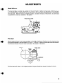
SET UP AND TESTING
VISUAL OBSERVATION is particularly important before attempting to repair a printer. Always
check for physical damage to the mechanism. Remove any loose debris that may have
accumulated inside the unit.
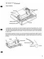
Ribbon Cartridge
PRINT HEAD
RIBBON CARTRIDGE
Before installing the ribbon cartridge, turn the printer off. By carefully pushing the carriage, position
the print head in the center of the unit. Turn the dial knob on the cartridge in the direction of the
arrow until the ribbon is taut. Insert the cartridge in the hooks provided and push down. The ribbon
must be positioned between the print head and the ribbon guide.
CAUTION!
When installing or removing the ribbon cartridge, do not touch the FPC cable. Check
that the FPC cable remains in the down position as shown.
FPC CABLE
2
SET UP AND TESTING (Continued)
Paper Installation
PAPER RELEASE LEV
To install paper, turn the printer off, remove the paper rack and lift the soundproof cover. Lift the
paper hold down shaft and raise the covers of the left and right tractors to allow access to the tractor
pins. Align the paper perforations with the tractor pins and close the covers. The left tractor assembly
must be firmly pressed against the left stopper. The right tractor assembly slides to allow adjustment
for paper width.
Once the paper is aligned in the tractor, turn the manual feed knob while guiding the paper to its position behind the platen (See the paper path figure below). Standard paper may be used by simply installing it in front of the tractor and behind the platen, using the manual feed knob to friction feed
the paper.
PAPER
TRACTOR PIN
TRACTOR FEED
- PLATEN
3
SET UP AND TESTING (Continued)
Self Test
This unit has a pre-programmed self-checking capability. The program may be used to test the print
head operation, print quality and printer mechanism (ribbon feed function, linefeed, etc.).
The self-test function is initiated by pressing the paper advance switch while turning on the power
supply switch. NOTE: Do not operate the self-test function in the no-paper condition.
*+ , - •
< :z >?~ABCDEFGH I JKLI'r'NOPQRSTUVWXY2 [
11'+-11.-...1 • . , It-. '-1 _ r'11'+-11.-...1 • . , It-. '-1 _ ~
"$%& • ( ) + , - • /01234~6789 I ; < .. )?~ABCDEFGH I JKL~PQRSTUVWXYl [ " 11'+-1.-...1 • . , It- .'-1 _ r'-T-i
$"/.& • ( ). + , -. /01234~6789: ,I < = >?~ABCDEFGH I JKLM'lOPQRSTUVWXYZ [ " If+-ll.-...1 • . , It-. '-1 _ r'-T-i I
X&· ( ) ... , -. /1211234:567891, < .. >?~ABCDEFGH IJKL~PQRSTUVWXYzr" 11'+-11.-...1 • . , 1t-.'-1 _r'-T-i I I
eSc' ( ) + , - • /EH 234567891 ; < = >?~ABCDEFGH r JKLMNJPQRSTUVWXYZ [ " 11'+-1.-...1 • . , It-. '-1 _ r'-T-i I I I
+ , - • /0 123456789 I ; < = )?@!ABCDEFGH r JKLMNOPQRSTUVWXYZ[ ''If+-ll.-...1 • . , It-. '-1 _ r'-T-i I I r
+ , - • /EH 23456789: ; < = >?~ABCDEFGH r JKLMNJPGlRSTUVWXY2 [ " 11'+-11.-...1 • . , It-. '-1 _ r'-T-i I I r+ , - • /e'l123456789 I ; < c >?~ABCDEFGH r JKLfw'NOPQRSTUVWXYl [ " 1l' +-1 .-...1 • . , It-. '-1 _ r'-rll I r-_
+ , -- • /121 1234~6789: ; < = >?~ABCDEFGH I JKLfw'NOPQRSTUVWXYZ[ '-.11'+-1.-...1 • . , It-. '-1 _ r'-rll I r--.J
t , - . /121123456789: ; < z >'?~ABCDEFGH I JKLI'1'IOPQRSTUVWXYl [ ''If+-ll.-..J • . , 1t-.'-1 _r'-rll I r---.J.
, -. /8123456789: ; <=>?~ABCDEFGH IJKLMNJPQRSTUVWXY2[ ''\1 l' +-1 .-...1 • . , 1t-.'-1 _r'-rll I r---.J. •
-. /121123456789 11 < ")?@!ABCDEFGH rJKLMNOPQRSTUVWXYZ[ "]t+-I.-..J • . , It- .'-1_r'-rl1 I r---.J. ...
• /01234567891 ) <: >'?~ABCDEFGH I JKLMNOPGlRSTUVWXYl [ ''It+-ll .-...1 • . , 1t-.'-1 _r'-rll I r---.J. ... .
/0123456789: 1< '" )?@!ABCDEFGHIJKLI'1'IOPGlRSTUVWXYl[" 11'+-11.-...1 • . , 1t-.'-1 _r'-rll I r---.J. .... ..
! H$"/.& • ( )
! "$"/'& • ( )
*
*+. - •
/01234~6789
: ;
/01234~6789 I ,
<.. >?@!ABCDEFGH I JKLI'r'NOPQRSTUVWXY2 [
"
"
*
'( )*
( '*
'*
*
SAMPLE SELF TEST PRINT-OUT
Additional Testing
A sample program should be run to test for proper interface operation. It is normally recommended
that the "customer complaint" be checked by verifying printer operation during print-out from an
appropriate program.
4
ACCESSORIES PARTS LIST
C 314597-01
C314598-01
C 314598-02
C 314598-03
C 314599-01
C 1 51 5001 -01
C 903508-04
1526/802/4023
1526
MPS802
4023
1526/802/4023
1526/MPS802
1526/802/4023
PAPER RACK
USER'S MANUAL
USER'S MANUAL
USER'S MANUAL
RIBBON
6PIN DIN CABLE
POWER CORD
MAINTENANCE
Cleaning
CAUTION
Do not use chemicals to clean any of the printer parts.
Using a clean, dry brush, remove dust and debris from the ribbon guide, print head, platen area and
tractors often. Periodically remove the top case and brush any accumulated dust or particles from
the unit.
Lubrication
CAUTION
Do not allow oil or grease to contact the motors, sensors, tractors, platen, ribbon
or print head.
Oil the carriage pillars, as indicated, every 500,000 lines or once a year. Use dry guaze to clean the
pillars before oiling. Oil sparingly and remove any excess. Use a light oil that will not attract and hold
dust and dirt.
LUB
A clean, light grease is used to protect the meshing parts of the plastic gears. Also, the 4 springs
on the unit may require lubrication. They can be found behind the paper guide, on the roller unit (2),
and on the paper holder (2). See disassembly numbers 12, 14 and 1 7 for identification. Be sure to
use lubricants sparingly.
5
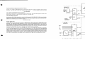
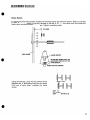
FUNCTIONAL BLOCK DIAGRAM
f--- RS (RAM SelECT)
----I
SERIAL 1526
INTERFACE
Functional Block Diagram Data Flow Theory
I
The 1526, MPS 802 and 4023 printers are functionally the same, with the exception of the interface
circuits. The 1526 and MPS 802 printers have a serial interface, and the 4023 printer has an IEEE
interface. The data flow is the same for all of the printers.
110
DATA
,~I
t----I PORT
nr.K
A
The 1526 and MPS 802 Serial Interface
I
AD - A61
----
ADDRESS
DECODE
r-r--
-S1 (SELECT 110 1)
S2 (SelECT 110 2)
LOGIC
r--
S3 (SelECT I/O 3)
ROM (SELECT ROM)
6504
MICROPROCESSOR
r--
I
RS
DRIVERS
DATA BUS
Processor Logic
B
B
PRINT
HEAD
Printable characters are stored in the LINE BUFFER. When the carriage return character is received,
all the characters stored in the LINE BUFFER are converted to DOT MATRIX codes by the operating
system. The OOT MATRIX codes are stored in ROM with the operating system. The DOT MATRIX
data is written into port B of U50. The driver circuits activate the proper print wires to form the
characters, one column at a time. As a character is being printed, the head (carriage) stepper motor
moves one dot column position at a time. A position sensor outputs pulses that are used to indicate
head position any time it is not home (far left). The paper stepper motor moves paper up one line
at a time when a carriage return is sensed. The operating system program monitors the position sensor output, and generates the signals that are passed to IC U60 port A controlling the motors.
I/O
I
I
I
I
AD -
---
--
J
I
4023 IEEE
NTERFACE
I
I/O
I
I
0101
I
--------------1
_______________-1 P
0
1
0108
RS
0
DAC
RFD
EDI
ATN
R
I
V
U8D
ROM
HEAD
MOTOR
I
1----.......- - - - -
IP
1--_-1
PAPER
MOTOR
10
U6D I R
65221T
HEAD POSTION DETECTOR
I A .....- - - - - - - - - - - '
I
HOME POSITION DETECTOR
I
L_
8K X 8
OPERATING t - - - - - - - - - - - - - I
SYSTEM
S3
I
----------------1
-----------------i TR
---------------4
DRIVERS
r -t----I
I
I
S1
Printer Data Flow
Parallel data from the interface is present on the data bus at times selected by the operating system
program. The operating system (program in ROM) monitors the data being received from the interface. Receive data can be printable characters or control codes. Printable characters are stored in
RAM. 256 bytes of RAM are available for character storage. 128 bytes of RAM are in U40, and 128
bytes in U5D. This RAM is called the TEMPORARY LINE BUFFER. Control codes are interpreted as
special function commands and are executed at the time they are received. The number of lines per
inch and the characters per inch are examples of special function commands.
PRINT
WIRES
(NEEDLES) t - - - I
PORT
DATA BUS
r---~ PORT
DEVICE
ADDRESS
SELECTION
:HEAD POSITION DET
___ L
128 X 8
I
1-
A~HUiOI~IME-;:;I':ru;ju:>llmllinul~IN DET
I
The 4023 IEEE Interface
Parallel data (0101-DI08) is received on the Port B inputs of U4D (PBO-PB7). U40 acts as a buffer,
allowing synchronization between the processor read operation and the receive data rate. Handshake
signals ATN (Attention), RFD (Ready for Oata), and DAC (Data Accepted) provide synchronization between the transmitting device and the printer.
U5D I
6532 I
I
128 X 8
1-----
~ t---.......--....I~UT~F PAPER INDICATOR
1-----
I
RS
PAPER FEED SWITCH
PAPER OUT
-
U7D
I t::
P
I0
AD _ A6-
'------I
I
I
U4D
6532
INVERTERS
Serial data is received at a rate determined by the clock input. The serial data signal is inverted, then
input to the IC U4D. IC U4D converts serial data to parallel data.
-
-
~TN
The Interface
I
I
I
ADDRESS
BUS
110
AD - A6
U4D
B
6532
--128 X 8
----,
E
R
S
P
0
R
T
I
DATA
BUS
1
I
I
I
I
A f
I
S1
I
I
I
I
I
__ J
6
CIRCUIT THEORY
CR26
_::-::-::-:4A:-'I/SO V or 1.S AlSO V
on
h.~t
sink
~-r:----r-:U)"""':::::
+5 V
N
-.
I'"
",I
uu
o"ai
L---~~~-+-~~-~---;uD
+5V GND
.
+.
RS
1--+_..::::::.+26 v
lO k
C7
6800
SOV
+26 V
GND
The Power Supply
The Power Supply generates two outputs, + 5VDC and + 26VDC. Both outputs are regulated. The
5VDC output supplies the microprocessor and TTL circuits. The + 26VDC output supplies the print
wire coils and the paper feed and carriage motor drive circuits.
+ 5VDC Supply
VR 1 is a series regulator. The series regulator keeps the output voltage constant when the load varies.
Capacitive filtering eliminates most of the ripple voltage on the output. CR26 is a full wave bridge
rectifier which converts the AC voltage generated from the top secondary winding of the power
transformer to DC voltage.
+ 26VDC Supply
A shunt type regulator circuit generates the constant 26 VDC output.
+26 VDC REGULATOR CIRCUIT
023
VOUT =019 VBE + VCR23
26.3V
R7
UNREG
DC
,=-
+26 VOLT
27V
C1
ILOAD
.7V
= -.7V +27V
OUTPUT
~
J
The output voltage is regulated at 26.3VDC because the base to emitter voltage of 019 opposes
the voltage developed across CR23. Most of the load current passes through the power transistor
023. CR27 is a full wave bridge rectifier which converts the AC voltage output from the bottom secondary winding of the power transformer to DC voltage. C7 filters the rectified DC output voltage.
7
CIRCUIT THEORY
RESET
UIC
1
_2
U20
3
~4
UIC 6
5
.~
_
UIC
POWER ON
7406
74LS14
Jl""o--;:4~_---:..;R:.:E.:.S-t-+-iI-+-i
+5V
+24 V
021
COLLECTOR
~
o
">::a£
APU
N "'>01
U1C5PIN
a: >ri
R21
~
U1C6PIN
Q21
--------
I, 100
~r,1-'
B I~>.... c:t
."
MN
U1C4PIN
I +5 V
-..:- +5 V
-
GNO
APPROX.
350 ms
Reset Logic Circuit Theory
A "low" pulse applied to the reset interrupt input, pin 1 of the microprocessor U7D, causes the processor to restart execution of the printer operating system program stored in the ROM USD. A reset
pulse occurs when the power is turned on. An external device connected to the serial bus can also
generate a reset, initializing all devices connected on the bus at the same time.
A short time after the power is turned on, the 5VDC supply rises to its normal operating level. This
forward biases Q21, allowing C3 to charge. When the voltage across C3 reaches 2 volts, the output
of the inverter U1C pin 6 goes "low", causing the output of the inverter U1C pin 4 to go "high".
This "low" pulse occurs when the unit is switched on. The reset input - RES - on the serial bus
(interface clear signal -IFC - on the 4023 IEEE interface) forces the reset pulse by applying a "Iow"
to the input of the inverter U 1 C pin 1.
S
1526 AND 4023 CIRCUIT THEORY
1.15
V1 .. MHz
2.2 "H
l..r----?": --0-1--'~:-~
,
-
.
C34
.04~
L _ ___ "
R56
R55
"o .,C!
"I'"
11
8
D--......::..j
74-00
7400
7400
7
U10C
74177
9
117
R57
1 MEG HZ
47
Clock Circuit
Crystal Y 1 generates the fundamental 4 MHz clock. The circuit illustrated below the crystal stabilizes
and squares the signal. U 1OC divides the input frequency by 4. A 1 MHz clock is output on pin 9
of U 1OC. This is the processor system clock.
9
1526 AND 4023 CIRCUIT THEORY
+26V
U5D
6532
Pl Jl
PAO
81PF Holdl
1. 14
PA4
PAS
2S 2S
61PMOI
7 (PM1)
0
B
W
M2
M3
0
ON
ON
OFF
OFF
1
OFF
ON
ON
OFF
2
OFF
OFF
ON
ON
3
ON
OFF
OFF
ON
4
ON
ON
OFF
OFF
A
R
0
U6D
6522
PA6
M1
R
2626
11
MO
F
A
81PM21
COIL
STEPPING
ORDER
M
3
27 27
0
282
0
N
T
I
PA7
IllPM31
9
IL _ _ _ _ _ .J
NOTE: DURING REVERSE
TRANSMISSION. THE
CURRENT FLOW IS
STEPPED IN REVERSE
ORDER - 4. 3. 2. 1. O.
PF Motor
Paper Feed Motor Circuit
The paper feed motor is a four phase stepper motor. Sequentially exciting two phases at a time causes
the motor to turn in step clockwise or counter clockwise. See timing chart above. Four outputs from
U6D,PA4-PA 7, activate the current amplifier transistors 013-016. Current flow through the emitter
collector junction of 013, through phase A coil, through the emitter collector junction of 017 via
the center tap motor coil excites phase A of the stepper motor. This occurs when the PA4 output
of U6D goes "low", U7B pin 4 goes "high", turning on 0 13. The PAO output of U5D must also be
"high", then U7B pin 2 is "low", and 0 17 is turned on. CR17 - CR21 suppress CEMF developed
by the stepper motor coils. This protects the current amps 013-016.
*WITH NO CR 17 - 21
COUNTERELECTROMOTIVE FORCE
APPROX. 100 V
*WITH CR 17 -21
26 V
I
.---r-COUNTER-
__
26 V=!~~~~""
L.
--"~_
ELECTROMOTIVE
FORCE
_ APPROX.
50 V
The stepper motor holds in position when the paper is not advancing. This occurs when a low value
current passes through 2 phases, producing opposing torques holding the motor in position. Phase
A and phase 0 are turned on, and 017 is switched off. Current flow is limited by the 470 ohm 5
watt resistor that is in parallel with 0 17.
11
CIRCUIT THEORY
,
+26 V
U5D
6532
J.
~~k ~
R3
3.9 k ?
Pl Jl
9 (CA Hold!
~
PA 11--------,-13"...., ?C:>:1:-::"2"""'1'r--+----f..... 018
U7B
R5
? 5 W 470 n
~~----~1313~
CR22
+~
~r(24 V!
lkx:Jcn~,
..... >
N~~C.~.N;»
~ {a:: ,a:: a::
PAO 2 (HMO!
--
~t-:!t-!!?
~t-t-i--f~
3 U6/B'O-:-4
~
r-----,
H-t
a:: a:: II-c: "a:: iI'
I
t.....=0:...+...:::O~O~~t;t.>~_--I21 21 ~-t--:.........
al0
3 (HM 11
""..0:-::;--_!---i_...r-t--.......-+---i~---I22 22~-~--'
PA 1 r--'-....:......-----,1...,-l1 ' 10
~ p12
I
U6D
U6B
I
6522
I
PA2r4~(H~M~2~1_ _-"....( >~~;-~_~~a;~~~--1232l~-~.........
13
12
__
" ' - 011
U6B
>~~
PAl 5 (HM3)
9
U6B
8
I
~
;
~
C
I~O
__-l_~~n;--~--12424~-~~
l1ro...... 09
L
I
- - _..J
CA Motor
71V
Carriage Motor Drive Circuits
U6D outputs signals HMO-HM3 (HM stands for head motor). Four outputs drive the four phases of
the stepper motor. This circuitry is similar to the paper drive motor circuits. 09-012 are current
amplifiers. The phase A coil is energized when 010 is turned on. Current is passed through the center
tap of the motor coil, through 018 to the 26VDC supply. The other three phases are controlled the
same way. The output PA 1 (CA Hold) goes "Iow", and 0 18 turns off when holding current is needed
to hold the paper in position. Two opposing phases are energized creating opposing torques holding
the motor in position. The holding currents from the motor coils return through R5 to the 26VDC supply.
R5 limits the current flow through the coils. CR13 through CR16 suppress the CEMF developed by
the coils in the motor protecting the output transistors 09-012.
12
CIRCUIT THEORY
Fl
5OO..s Puis
...
~;"':;";;"""'---3>~TP1_>-----,
680nx8
CR12
CR9
CR6
CR3
(24 VI~~
~~ ,,;~
~~
L
Jl
10 10
11 11 t------~
PB7 241N071
S
U6B
PB6
r2.;;,.3.,;. IN.. ,:O.. .:6..:. . 1- d
1
>2=----'-+-+-+-+--+--t---i",-- 07
USB
6 6
PBS 221NOSI
13
U5D
6532
PB4 21 IN041
7 7 r - - 00 0 cf'-
-
OClQO"\-
12
USB
'"::-:::----"-"""-i--+-+-+---i ......---lr---.L-..+-+-+-+---! S S r - - 0000 "\11
..... ,0
" ' - - OS
PB3 '91N031
S
USB
PB2 181N021
3
4
USB
PBl r'.,;..7.;.;.IN,;.;:O;...;,'.:....'- d
:>-::--_ _ _ _ _......-f--f ......- t - - - - - - - - - - . l - - I - - - - I 2
1
2
~ 02
USB
PBO 161NOOI
9
~-r-------~--~ 1
01
~8---------I.--I",--
2 I-_~~~~
000 /j L.....
1
0000'Top plate
.print Wire Drive Circuits
U5D outputs eight signals NDO - ND7 (ND = Needle Drive) from parallel port B (PBO - PB7). These
signals are inverted by U5B and U6B. The output of the inverters control current amplifier transistors
Q1 - Q8. A print wire (needle) is fired when an output transistor is forward biased, allowing current
to flow through the coil from the 26VDC supply. CR 1 - CR 12 suppress CEMF developed by the coils.
The inverters U5B and U6B are 7406 open collector Hex/Inverters. A one shot circuit generates + VCC
for U6B and U5B for 500 microseconds when a print wire is fired. This protects the print wire coils
by limiting the current through the coils. See Coil Protection Circuit and Timing on page 14.
13
CIRCUIT THEORY
•
+5V
PBo~1~0--~-----+-~2
r
Triger
Rewt
U6D
4
>--+_"""1
V~
Reset circuit
rewt
r--_-+-----.,;6:..j TH
6522
OUT 1-"3_..JV'''---I
uaa
CR28
R39
7
20 kn"loE----~DIS
022
.----~TPl
R23
3.9 k
GND
C8
.r.
0
10
R37 2.2 k
555
cv
5
TIMING CHART
+5V
'.'"
JLs
-tt-
~U~6~D.~P~BO~----·U~-----------------
USB·OUT
Q22·COllECTOR
TP1
I.
500
JLs
.1
Print Wire Coil Protection Circuits
When a print wire is fired, the output PBO on U6D goes "low". This triggers the 555 USB. The output
pin 3 goes "high" for 500 microseconds. This turns on 020,021, and 022. The potential developed
at the collector of Q20 is used as + vee for the open collector Hex/Inverters U5B and U6B. R39 should
be adjusted to obtain the 500 microsecond pulse.
14
CIRCUIT THEORY
+5 V
P1 PJ
R12
15 K
NO-PAPER SENSOR SWITCH
PA2~1_0--------------~----~1818~----o
U5D
(6532)
1616~----------~
+5 V
R54
470
P3 J3
n
PA3~1_1____________4-____~1
PF KEY
1
U2D
PA5 ~1_3____a >---~----~ 3 3
1
2
U5D
(6532)
~--;)I------+
PAPER ADVANCE SWITCH AND INDICATOR CIRCUIT
Paper Control Logic
A normally closed micro switch located behind the platen opens when paper is loaded in the printer.
When no paper is in the printer, the switch is closed causing a "Iow" potential to be input at U5D
pin 10 (PA2).
Depressing the push button on the front of the printer causes a form feed to occur. Form feed length
is software controlled. A "Iow" potential is applied to U5D pin 11 (PA3) when the push button is
depressed. An LED inside the push button case indicates the printer is powered on. A flashing LED
indicates paper out. The output U5D pin 13 goes low" , U2D pin 2 goes "high", and the LED turns on.
II
15
CIRCUIT THEORY
+5V
Rll
47 k
R9
150 n
Rl0
47 k
U5D
6532
PA6
U1C
9
8
14
Pl Jl
12 12
,.,
19 19
U1C
20 20
~~--~--~t5
U6D
6522
"'"
CARRIAGE POSITION SENSOR
HOME POSITION SENSOR
t5~----~----~
iii
c:
u;
'"
....:
CAt 40 -
iii
c:
s-
I/)
CA2
1=-39~-J
a:
TIMING CHART
*TIMING SIGNAL
--------lnn
_______ __ UUL
U1C-9 PIN
)I
U1C-8 PIN
(PA6)
"
APPROX. 1.5 ms
inn nnnrr - - - - -- - -n n
uuuuUUL _______ --.J UL
PLACE MAGNET CURRENT
FLOW OPENING POSITION
1\
*RESET SIGNAL
-=U~1C~-~1~1~P~IN~____________________________~)
PLATE MAGNET
CURRENT FLOW
OPENING POSITION
FOR THE NEXT
LINE.
~~_____
U1C-10 PIN
(PA7)
WHEN CARRIAGE HAS
RETURNED TO ITS
HOME POSITION
PRINT STOP SIGNAl)
PRINT START
SIGNAL FOR NEXT
LINE PRINT
Position Sensor and Home Sensor Circuit Theory
When printing, the print head moves across the paper on the carriage assembly. The carriage assembly
is driven by a carriage stepper motor. As the stepper motor turns, a photo-coupler device generates
"low" pulses which are input to U 1 C pin 9. U 1 C is an inverter. U 1 C generates "high" active pulses
which are input at U5D pin 14 (PA6), and U6D pin 40 (CA 1). A subroutine in the operating system
monitors the pulses generated by the photo-coupler, providing processor controlled print head positioning. A second photo-coupler device provides a synchronizing pulse or a start pulse when the print
head is at the far left (Home) position. The output of the photo-coupler is input to U 1 C pin 11. The
output on pin 10 is input at U5D pin 15 (PA5) and U6D pin 39 (CA2).
16
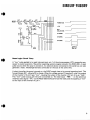
1526 AND MPS 802 CIRCUIT THEORY
+SV
1 kn x 4
P5/P6
u;
Serial Interface Connector
a::
U2C
SQR
ATTN
2
8 PAO
r--t-------....,---=1
3
U2C
Clock 4
5
PSIP6
6
U4D
6532
U2D
10
p..:-;'-+.--=...oc
Signal
Pin No.
1
SERIAL SRQ
2
GND
3
4
SERIAL ATN
5
SERIAL DATA
6
RES
t-_ _ _ _....;1~3 PAS
U2D
8
r9 _ _ _ _---.:'....:..j4 PA6
U2C
Data
5 1--_---01---.:1:..;..1d
~10=-----------':..::.j5 PA7
SERIAL elK
RST
6 /-------0
GND 2
Reset circuit
-=- FG
TIMING CHART
A~ _ _ _ _ _ _ _ _ _ _ _ _~
RECEIPT OF MESSAGE
RECEIPT OF DATA
PAS HIGH (PRINTER READY)
The 1526 and MPS 802 Serial Interface Circuit Theory
The serial interface has bi-directional DATA and CLOCK signals. SQR (Service Request) is a handshake input that is not used. ATTN (Attention) is a "Iow" active handshake signal. The printer accepts data on the DATA input (pin 5 of P5 and P6) after the ATTN input (pin 3 of P5 and P6) goes
"Iow". U2C pins 2 and 3 go "high", U2C pin 4 goes low
U2D pin 12 goes "high", and U2D
pin 10 goes "Iow". This is the DATA output which acts as an acknowledgment to the ATTN input.
When the printer becomes ready to accept data, U4D pin 13 (PA5) goes "high", U2D pin 6 goes
"Iow", U2D pin 10 goes "high". ATTN kept "Iow" by the transmitting device indicates commands
are being transmitted on the DATA line. When ATTN is "high", data is being transmitted on the DATA
line. Data is input on U2C pin 11. The output of the inverter U2C pin 10 is input at U4D pin 15 (PA 7).
Data is clocked into the printer at the rate specified by the signal on the CLOCK input (pin 4 of P5
and P6l._ The Clock signal is inverted by U2C, then input at U4D pin 9 (PA 1). An external reset will
reset the processor logic inside the printer. RESET is on pin 6 of P5 and P6.
II
•
II ,
17
4023 CIRCUIT THEORY
P2
i.1
PATTE~N
I
JUHf>£1?
SHORT ALL
The 4023 IEEE Interface Circuit Theory
All the signals on the interface are controlled by the I/O device U4D. Eight parallel bi-directional data
lines (PBO-PB7) are used as the parallel data bus for the interface. DAV (Data Valid) pin 6 of P2 is
a "high" active output from the transmitting device. Valid 8 bit codes are transmitted to the receiving device when DAV is "high". DAC (Data Accepted) pin 8 of P2 is an output that is "low" when
data is being accepted because U4D pin 10 (PA2) is "high". RFD (Ready for Data) pin 7 of P2 goes
"low", indicating the printer is ready to receive data when data is not being accepted (DAC is "high"),
and U4D pin 7 (PA 1) is "low". ATN pin 11 of P2 is an input. The transmitting device brings this line
"low" before the data is transmitted. EOI (End or Identify) pin 5 of P2 is an input. The transmitting
device brings this line "low" when the last byte of a message is being transmitted. IFC (Interface
Clear) pin 9 of P2 is an input. An external reset signal applied to the IFC initializes all the printer processor logic.
18
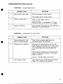
TROUBLESHOOTING GUIDE
SYMPTOM 1:
Printer does not initialize when powered up.
POSSIBLE CAUSE
SOLUTIONS
1.
Power cord is damaged.
Check that the power cord is connected properly
and is in good condition.
2.
Power switch is broken.
Check and replace it if necessary.
3.
Fuse is blown.
Replace it. If it blows again, check the power
supply unit and PCB.
4.
Power supply is defective.
Check for proper voltages at the PIS connector
J4.
5.
Defective logic board.
SYMPTOM 2:
AC Volts
Across Pins
Cable Color
26
1 and 4
Orange
9
2 and 3
Red
Check for shorts on PCB. See circuit theory on
page 7 for proper operation of power supply
circuit.
Printer initializes but will not print.
POSSIBLE CAUSE
SOLUTIONS
1.
Ribbon cartridge is missing or
empty.
Replace ribbon.
2.
Paper out condition is present.
Check that paper is properly inserted.
Check paper out switch and replace if necessary.
3.
Bad connection between PCB
and Mechanical assembly.
Check mechanical connection at P1 on PCB.
4.
Data transmission is not
complete.
Check serial or IEEE cable for proper connection.
Check for proper data transmission from
computer.
Check interface circuits on PCB. See circuit theory
on pages 18 and 19.
19
TROUBLESHOOTING GUIDE (Continued)
SYMPTOM 3:
Part of a printed character is missing.
POSSIBLE CAUSE
SOLUTIONS
1.
Ribbon is worn out.
Replace the ribbon cartridge.
2.
Head shift lever is out of
position.
Re-set the shift lever.
3.
Print head on flexible cable is
defective.
Check flexible cables and wiring harness for
continuity.
Check the print head by disconnecting the wire
harness connector J 1 from P1. With an ohmmeter
set on the 200 ohm range, place one of the leads
on pin 10 of J 1 and the other lead on pins 1
through 8 of J 1. A resistance of 10 to 14 ohms
at each pin indicates a good print head. Replace if
necessary.
4.
Interference (NOISE) in the
proximity of the printer.
SYMPTOM 4:
Paper does not feed correctly.
POSSIBLE CAUSE
1.
Place printer in area void of external interference
(i.e., motors, machinery).
Physical interference with
proper paper feed.
SOLUTIONS
Check for obstruction of the paper feed path paper guide, platen, tractors.
Check that the left tractor is positioned to the extreme left and the right tractor is adjusted to the
correct paper width.
Check that the paper holes align with the tractor
pins correctly.
Check that the paper release lever is in the correct
position - in the direction of the arrow for tractor
feed or opposite the arrow for friction feed.
Check that no more than the maximum allowable
sheets of paper are being used.
2.
Paper feed motor defective.
With power off, check motor with an ohmmeter.
Set on the 200 ohm range. A good paper feed
motor should need around 50 ohms between pin
14 of J1 and pins 25,26,27, and 28 of J1.
Check for good mechanical and electrical connections to the motor and its wiring - see wiring
diagram on page 28.
Check for + 26 VDC supply to the motor.
3.
Circuit failure on PCB.
Check motor circuitry on PCB. See circuit theory
on page 12 for proper circuit operation.
20
TROUBLESHOOTING GUIDE (Continued)
SYMPTOM 5:
Improper Ribbon Feed
POSSIBLE CAUSE
1.
Obstruction of ribbon path.
SOLUTIONS
Check FPC cables for proper location.
Check ribbon guide for foreign matter.
2.
Defective ribbon cartridge.
Check for proper ribbon insertion.
Check the rotation of the cartridge by manually
rotating the ribbon in the direction of the arrow.
3.
Defective mechanics.
SYMPTOM 6:
Check the ribbon drive gears for proper lubrication
(see page 5) and smooth opertion.
Carriage does not move correctly.
POSSIBLE CAUSE
SOLUTIONS
1.
Physical obstruction in the
path of the head carriage.
Check that dirt or foreign objects have not
accumulated within the mechanism.
2.
Carriage motor is defective.
With power off, check the motor with an ohmmeter. Place one of the leads on pin 13 of J 1 and
read the resistance to pins 21, 22, 23 and 24 of
J 1 . A good carriage motor will read about 50
ohms.
Check for good mechanical and electrical connections to the motor and its wiring - see wiring
diagram on page 28.
Check for + 26 VDC supply to the motor.
3.
Circuit failure on PCB.
Check motor circuitry on PCB. See circuit theory
on page 12 for proper circuit operation.
21
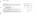
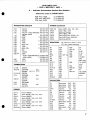
PCB PARTS LIST
• 1526 • MPS 802 • 4023 •
C - Indicates Commodore Stocked Part Numbers
Differences noted in PARENTHESIS!
PCB Assy 1526
PCB Assy MPS 802
PCB Assy 4023
INTEGRATED CIRCUITS
U1C
Ul0
U2C
U20
U40
U5B
U50
U6B
U60
U7B
U70
U8B
U8C
U80~
U9C
Ul0C
DIODES (Continued)
74LS14
74LSOO
74LS14 (1526, MPS 802)
74LS04 (4023)
7406
C
6532
7406
C
6532
7406
C
6522 VIA
7406
C
6504 CPU
555
74LS42
2364
ROM (1526/MPS 802) C
ROM (4023)
C
7400
74177
901521-30
901521-01
901521-30
901521-02
901522-06
901458-01
901522-06
901458-01
901522-06
901437-01
901522-06
901455-01
901523-01
901521-17
325341-08
325360-03
901522-04
901522-03
TRANSISTORS
01-08
09-016
017,018
019
020,21
022
023
2S0837
sub:
2S0946B
2S0985 5k ~37D JI.~J2SB794
sub:
2S0946B
2S0985
2SA733
sub:
2SA844
2SC2308C
sub:
2SB705
2SA1075
DIODES
CR1,2
CR3
CR4,5
CR6
CR7,8
CR9
CR10,11
CR12
CR13-20
Power IN4002
Zener R024F, 24V,
Power IN4002
Zener RD24F, 24V,
Power IN4002
Zener RD24F, 24V,
Power IN4002
Zener RD24F, 24V,
Power IN400
C314584-01
C 314584-02
C 314585-01
lW, 10%
1W, 10%
1W, 10%
1W, 10%
CR21,22
CR23
CR24
CR25
CR26
CR27
CR28
Zener R024F, 24V, lW, 10%
Zener HZ27-2 .5W
Switching 1S2076
Zener HZ4B-2 .5W
Stack KBP02 Sub: S2VB 1.5A
Stack KBL02 Sub: S4VB 4A
Switching 1S2076
RESISTORS -
Rl
R2
R3
R4
R5,6
R7
R8
R9
Rl0,11
R12
R13
R14-19
R20
R21
R22
R23
R24,25
All values are in ohms- 1/4 W
5% unless noted otherwise.
3.9K
10K
3.9K
10K
470, 5W 10%
820
10K
150
47K
15K
10K
680
3.9K
100
10K
3.9K
680
R26
R27-35
R36
R37
R38
R39
R48
R54
R55,56
R57
R61-64
2K
lK
3.9K
2.2K
22K
Variable
20K,
EMV-K4G
1K (4023
only)
470
680
47
1 K (1526,
MPS802
only)
CAPACITORS
Cl
C2
C3
C4-6
C7
C8
C9
C10
C11
C19-25
C26
C27
C28
C29
C30
Electrolytic lOOItF, 35V
Electrolytic
1OItF, 35V
Electrolytic lOOItF, 16V
Ceramic
.1ItF, 12V
Electrolytic 68001tF, 50V
Ceramic
.01ItF, 50V
470pF, 50V
Ceramic
Ceramic
.1ItF, 12V
1000pF, 50V
Ceramic
Ceramic
.1ItF, 12V
Electrolytic 4 7OOItF, 16V
Ceramic
.1ItF, 50V
Ceramic
.1ItF, 12V
Electrolytic 33OItF, 16V
Film
.1ItF, 100V
22
PCB PARTS LIST
• 1526 • MPS 802 • 4023 • (Continued)
C - Indicates Commodore Stocked Part Numbers
CAPACITORS (Continued)
C32
C33-34
C35
C36-37
Ceramic
Ceramic
Ceramic
Ceramic
200pF,
.047p.F,
.01p.F,
470pF,
MISCELLANEOUS (Continued)
50V
50V
50V
50V
P3
P4
P6,P7
MISCELLANEOUS
Ferrite Beads
1526/MPS802
L1
L3-6
L15-17
Y1
P1
P2
4023
L 1, 2
L4-14
L 15-17
VR1
28 Pin Connector
IEEE-48 Rt. Angle Connector
C 903206-01
(4023)
3 Pin Keyed Header
4 Pin Connector
C 903361-01
6 Pin DIN Connector
(1526/MPS802)
Regulator 7805
Shield Box
Shield Cap
C 4022048-01
C 4022047-01
Crystal 4 MHz, HC18V
23
1526 • MPS 802 SCHEMATIC
r-----
i ~ ""-
2 2
,
+Sy
~!
(}7D /( (>'(
.----
~~
-
Itt
~~~, ~k" £
: ~:~ .. ",,...-~ ~,-., ]7-
,,~
~
!
------------------------,
m/-iiiS
~
I
0~~~
~
c<
tk"'''',,,-_:,-I+-~ +-J-V
.w
"7
L ____________________________
!
i
I
~
.. i .. ~
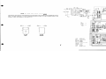
1526 • MPS 802 ROM UPGRADES
..
The PCB for these printers was designed to accommodate a 24 pin ROM or 28 pin EPROM at location
USD. A jumper change at J 1-J4 will configure the board for either I.C. When changing chips at this
location, match the jumpers to the type of I.C.
~
J2 CLOSED
• J4 OPEN
.-~
•
OPEN
J1.
•
CLOSED J3 • ~
•
~
.,....-.
• J2 OPEN
J4 CLOSED
~
. .: : :;q-. ~()()>Lj-i-~ ~\~ ~::UJJI.t:"'~"v'·_J<Z. MZ. 1
ULfD
+~y
CLOSED J1 ~
OPEN
J3.
•
L-_____
U
)I
c:
U2C
~I
( r::"?'"
O....-l ../ r
]:
,
U8D
24 PIN
28 PIN
ROM
EPROM
C~26
: K/JP02/S2V/J
(~
: J:8L 02 / S<1- V/J
27
\)9", Q/~
I
: 2SD98S/2J'D'I?-6B
019
o ! ~ Q8
: 2SI) 80$ 7
Q2() ,Q.2!
'2JIJ.r6!
Q 22
: 2SC 2..708
QI7, QI8
: 2SB 7'1'1
Q.23
: liB 7#/,2SA/nS
C, 1,2 'I : /N.OO.2/,w,ti.SE!w()&1J
.s,7.IO,f/
N
-.j()
28 :
(;'3,6,9 :
~.L4,
I
IS~076
~i).24F
12,21,22
CII 23
: H~ 27-2
C~ 2$
:H2 '18-2
VR /
: AN 710s
l~jOS
24
4023 SCHEMATIC
"11)
r----------------------------------------iI
:
,
I
J~:-=~ ~
ii¥S .L'nr
1
1
2
nM~
~--'
~-dH-~
r-zr,:>$'1~
4
I ~:k~
r...~
.~~
A.#
,..tJ.ii9-F~
:
I
...4-=.j
~.,
~·n
-
~~.,..,
:~I~
-{.
<J6
~
".V'"
,.,.,"1'1
.L!?
~
+4'V
~
'--H'
vtoC'
.,.,
M'7
IL "~"t
______________________________________
?
~
HM
i
IV~
,i
Nt)2
:,
-Hel
~
iV.IIT
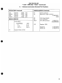
DEVICE NUMBER CHANGE
The 1526, MPS 802, and 4023 are shipped from the factory set for device #4. The channel can
be hardware altered to #5,6,7,8,9, 10 or 11 by lifting the indicated pin or pins of the 6532 at
location U4D.
APII
z_-PI
DEVICE #
1526 • MPS 802
4023
""
5
6
7
8
9
10
11
24
23
23 and 24
22
22 and 24
22 and 23
22, 23 and 24
11
12
11 and 12
13
11 and 13
12 and 13
11, 12 and 13
"100
Y
~
1
..
.
~
,~
6
I
c/{.1l
KBI'
c/{.n
Q9~
2JtJ,'S/2.li>'lU8
r;J/9
Q/ -
Q
8
Q20. Q.21
Q22
017. 0/8
Q2:l
CR t. 2. <f
CR MOTOR
oj/.1'2 ye
KUo2/J~Y8
916
U
I
I
.2S'J) II.n
: .2S11~61
: -.Lse 2ao8
: 2SIJ 7H
: 2.J.6 70s /.MA /I1?S
: IN_.2 /1l>S;.#'E/wHIJ
..t.7,IO,l1
/oJ -..J()
CI?.1f. •.18 : IS.2 .. .,&
(1:.4.6.': IU)~F
12 • .2/..12
: HI.27-2
(11M
: HI ~-2
au'!
:AN7I1S
Vit I
PE SENSE
~
25
ADJUSTMENTS
Head Shift Lever
The head shift lever controls the position of the print head in relation to the platen. With the lever
in its lowest position, towards the front of the printer, the print head is positioned as far as possible
from the platen. With the lever in its highest position, towards the back of the printer, the print head
is positioned as close as possible to the platen.
HEAD SHIFT LEVER
Print Head
Set the head shift lever in its lowest position on the right side frame. Position the print head so that
the clearance between it and the platen is 0.5 mm ± 0.05 mm. Tighten all screws and nuts and recheck
the distance between the print head and platen. Re-adjust if necessary.
PLATEN
PRINT HEAD
With the head shift lever in its highest position the gap should be reduced to about 0.4 mm.
26
ADJUSTMENTS (Continued)
Home Sensor
To adjust the print start position, loosen the mounting screw for the home sensor. Slide it to the left
or right, so that the center of the dot farthest to the left is 32 ± 1 mm away from the inside left
frame when printing standard characters. Tighten mounting screw .
• 32±1MM
0
0
H
0
0
0
0
SIDE FRAME
HOME SENSOR
ADJUSTING SCREW FOR THE
MOUNTING POSITION OF THE
HOME SENSOR.
Using the self-test, check for the position of the
leftmost dot. If alternating lines are not within
0.32 mm of each other, re-adjust the home
sensor.
-+1,.,......>-
0.32
OR
LESS
Ii
0.32
H
H
-H--
WITHIN 0.32
27
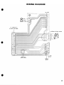
WIRING DIAGRAM
FPC CABLE
-----'--;~~
HOME
I SENSOR
~
I
'---RED- -
_J
'-'-BLACK-. . . . -YELLOW-
A
EK
- ! -C
I
I
I
I
TO
ON
CONNECTOR PI
MAIN LOGIC BOARD
CARRIAGE POSITION SENSOR
C-- -
-=:LH~~:~:,~¥C~E
c~ AI
s-- --
~J
BLACK
...
--
_..... ...
K
...
--RED"'- - -
Y
B
W
R
G
G
PAPER OUT
MICRO SWITCH
PAPER FEED
MOTOR
CARRIAGE
MOTOR
28
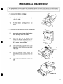
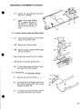
MECHANICAL DISASSEMBLY
The phillips head screws used in the printer mechanism are metric size. Use caution when selecting the proper size screwdriver.
1. To remove the ribbon cartridge:
1 .1
Position the right side tractor assembly
to the far right.
1.2
Lift the ribbon cartridge from the
printer.
1.1
2. To remove the top case and printer mechanism:
2.1
Remove the manual paper feed knob by
firmly pulling it from the shaft.
2.2
Stand the unit up, as shown, and
remove the 4 case screws at the corners. If the 2 center shipping bolts are
still in place, remove them.
2.3
Using both hands, support the top case
while lifting it up and towards the back
of the unit.
2.4
With the top case tilted toward the
back, lift the switch connector from the
PCB.
2.5
Remove the heat shield to expose the
PCB.
29
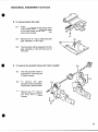
MECHANICAL DISASSEMBLY (Continued)
2.6
Detach the wiring harness connector
from P1 on the PCB.
2.7
Loosen the 3 large phillips
head screws at the front of
the mechanism. Sliding the
mechanism towards the
front, lift it from the bottom
case.
2.7
3. To remove the print head and ribbon guide:
:~,
~~
('-8-.1
,I
~
'" - -3:'5
Set the head release lever to its lowest
position on the side frame.
Remove the 2 head screws.
By gently pulling, detach the FPC cable
from its connector.
Lift the print head from the carriage .
...:,; ; :/ .~
; (;,.:t;:6
Remove the ribbon guide screw.
Lift the ribbon guide and head insulation sheet from the carriage.
4. To remove the paper detection switch:
4.1
Remove the switch bracket screw.
4.2
De-solder the micro switch wires from
the wiring harness PCB. (See wiring
diagram on page 28).
4.3
To detach the switch bracket, remove
the screw from the micro switch.
30
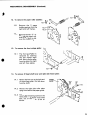
MECHANICAL DISASSEMBLY (Continued)
5. To remove the home position sensor:
5.1
Remove the sensor PCB screw.
5.2
De-solder the wire connections
from the wiring harness PCB. (See
wiring diagram on page 28).
5.3
Slide the sensor PCB toward the
front of the mechanism, pulling it
from its bracket. Turn it sideways
to fit between the carriage pillars.
6. To remove the paper feed motor assembly:
6.1
Remove the 3 motor bracket screws
from the right side -Frame assembly.
6.2
De-solder the wire connections from
the wiring harness PCB. (See wiring
diagram on page 28).
7. To remove the carriage position sensor and carriage motor:
7.1
7.2
Remove the sensor PCB screw and desolder the wire connections from the
wiring harness PCB. (See wiring
diagram on page 28).
Remove the carriage motor screw as indicated. Detach the carriage motor and
its holder by carefully bending the
bracket legs to release them from the
base.
HEAD
CARRIAGE
MOTOR
7.2
REMOVE
SCREW
7.3
De-solder the motor wires from the wiring harness PCB. (See wiring harness
on page 28).
31
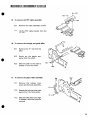
MECHANICAL DISASSEMBLY (Continued)
8. To remove printer drive belt:
8.1
Position the carriage at the center of the
unit to allow access through the base
to the belt holder screw. Remove the
screw and bracket.
8.2
Remove the liE" clip to release the belt
gear assembly on the right.
8.3
The drive belt will be released from the
gear assembly on the left and can be
removed.
9. To remove the sprocket frames and tractor assembly:
9.1
The left sprocket frame is
detached by removing the
2 frame screws.
9.2
9.2
To remove the right
sprocket frame assembly,
remove the 2 frame screws.
9.3
Remove the liE" clips to
release the tractor assembly from the sprocket
frames.
32
MECHANICAL DISASSEMBLY (Continued)
.
1--10.1
10. To remove the platen cover:
10.1 Remove the 2 cover
screws, as indicated. Lift
the cover off of the platen.
11. To remove the platen and reduction gears:
11.1
Remove the "E" clip and pull the
reduction gear off of the frame.
11.2
Remove the spring pin from the platen
gear by tapping it with a punch.
Withdraw the gear from the platen
shaft.
11.3
Remove the platen washer and shaft
supporter that are now exposed.
33
----------------------~--
-
-
MECHANICAL DISASSEMBLY (Continued)
12. To remove the paper roller assembly:
q tl
12.1-(1
12.1
Remove the 2 paper
holding springs from the
right and left frames.
12.2
Remove the left liE" clip
and pull the paper roller
axle to enable it to slide
over the frame pins.
G
~
13. To remove the front carriage guide:
13.1
The front guide pillar is
removed by loosening
the hex nuts at each
end. Next, slide the pillar
"from its slots in the right
and left frame plates.
14. To remove the head shaft lever and right side frame plate:
14.1
Remove the hex nut at the right end
of the carriage pillar. Pull the lever
from the shaft.
14.2
Remove the right side roller plate
spring from behind the paper guide.
14.3
Remove the remaining screws in the
frame plate. The frame must slide
back, out of the base, to be removed.
FRAME
PLATE
34
MECHANICAL DISASSEMBLY (Continued)
,-15.1
I
15. To remove the FPC cable assembly:
15.1
Remove the cable assembly screws.
15.2
Lift the FPC cable bracket from the
carriage.
15.2
16. To remove the carriage and guide pillar:
16.1
Remove the "E" clip from the
pillar.
16.2
Gently pry the plastic supporter from the shaft.
16.3
Slide the pillar to the right to
release it from the frame.
17. To remove the paper roller assembly:
17.1
Remove the release lever
screw and the lever assembly.
1 7.2
Release the left side roller plate
spring from the frame plate.
17.3
Slide the roller plate to the right
to release it from the frame for
removal.
35
MECHANICAL DISASSEMBLY (Continued)
18. To remove the platen and paper guide:
18.1
Remove the "E" clip from the platen
shaft.
18.2
Pull the platen washer and shaft supporter from the platen shaft.
18.3
Slide the platen to the right to clear the
side frame.
18.4
Remove the paper guide screw from
the side frame. Slide the paper guide
to the right to clear the frame.
19. To remove the gear plate assembly and left side frame:
19.1
Remove the 2 plate screws from the
assembly.
19.2
Remove the "E" chip from each gear
and lift the assembly from the frame.
19.3
Remove the remaining left frame
screw and slide the frame to release
it from the base.
ASSEMBLY NOTES
To reassemble the printer mechanism, reverse the oraer of disassembly and follow these precautions:
•
The print head must be insulated from the carriage assembly. Check it with an ohmmeter.
•
Lubricate all gears and springs as instructed on page 5.
•
Secure all screws with a self-locking liquid.
•
Make adjustments, as required, per the procedure on pages 26 and 27.
36
CASEWORK Section 1. Casework/Power Supply
MECHANICAL ASSEMBLIES
REF. NO.
1-1
C 31458001 1526/802/4023 SOUNDPROOF COVER
C 31458101 1526 TOP CASE
1-2 C31458102 MPS802TOPCASE
C 31458103 4023 TOP CASE
1-3 C 31458201 1526/802/4023 PLATE ASSY
1-Plate w/Paper Advance Switch
2-Lamp, PCB and Harness
C 31458301 1526 BOTTOM CASE W/PWR/SUP ASSY
1-Plastic Case, Ground Plate and Cover
2-Power Supply Assy
1-4 C 31458302 MPS 802 BOTTOM CASE W/PWR/SUP
ASSY
1-Plastic Case, Ground Plate and Cover
2-Power Supply Assy
C 31458303 4023 BOTTOM CASE W/PWR/SUP ASSY
1-Plastic Case, Ground Plate and Cover
2-Power Supply Assy
1-5 C 314600-01 1526/802/4023 PAPER FEED KNOB
37
SECTION 2. MECHANICAL ASSEMBLIES
SECTION 2. Mechanical Assemblies
REF. NO.
2-1
C 31458601.
~-'
1526/802/4023 PRINT HEAD ASSY
1-Print Head
2-Flexible Cable
2-2
C 31458701
1526/802/4023 CARRIAGE ASSY
1-Carriage w/Guide
2-Carrier Guide Pillar
3-Head Adjust Lever
2-3
C 31458801
1526/802/4023 PLATEN ASSEMBLY
1-Platen w/Upper Cover
2-Paper Guide
3-Roller Plate w/Release Arm and Button
4-Pressure Roller Unit
2-4
C 31458901
1526/802/4023 TRACTOR ASSEMBLY
1-Paper Holders L&Rt
2-Pin Feed Rollers (2)
3-Tractor Shaft
2-5
C 31459001
1526/802/4023 GROUND PLATE ASSEMBLY
1-Bottom Ground Plate
2-Side Ground Plates (2)
3-Sprocket Frame Left
4-PCB w/Harness and Flexible Cable
2-6
C 31459101
1526/802/4023 GEAR REPLACEMENT KIT
1-AII Plastic Gear Parts
2-7
C 31459201
1526/802/4023 SENSOR ASSEMBLY
1-Home Position Sensor w/PCB
2-Carriage Position Sensor w/PCB
3-Paper-Out Microswitch
C 31459301
1526/802/4023 HEAD MOTOR ASSEMBLY
1-Motor w/Holder
2-Rotation Detector
2-8
~
!
'
2-9
:: ( .
2-10
{-.
,"
;.'
;1/:~.
C 31459401
r:<r:; - '),r.'
1526/802/4023 LlNEFEED MOTOR
1V;fo;
C 314~~5_0).,
1.526/802/4023 CARRIAGE DRIVE BELT
1/4C 31459601
1526/802/4023 HARDWARE KIT
1-Miscellaneous Screws, Washers and Nuts
2-Miscellaneous Springs and "E" Clips
3-Miscellaneous Plastic and Rubber Pieces
(:: commodore
COMPUTERS
Da t e:
DOCUMENT REGISTRATION
M an ua l Nam e:
Part Nu mber:
Issue Da t e:
The return of t his inf ormation is essential to t he m ainte nance of you r docu m entation. If necessary , document upd ate s and ch anges w ill be distributed to regi stered perso ns. Subseq uent versi on s an d editi ons
of this do c um ent m ust be purchased .
Na me: _______ _ _ _ _ _ __ _ ____
Com pany : _____ _ _ _ _ _ _ _ _ _ __
St reet: ___________________
Cit y : __________________
State : _ _ __
Tear Here
Zi p : _ __ __
PLACE
ST AMP
HERE
COMMODORE BUSINESS MACHINES
C-2654
West Chester, PA
Service Documentation
19380
c~ commodore
COMPUTERS
DOCUMENT CHANGE RECOMMENDATION
THIS FORM PROVIDES OUR CUSTOMERS WITH AN EASY METHOD OF SENDING IN DOCUMENT CHANGE RECOMMENDATIONS. JUST REMOVE, FILL IN, AND MAIL THIS FORM. OUR
STAFF WILL REVIEW ALl. RECOMMENDATIONS AND, WHEN APPROPRIATE, MAKE THE
THANK YOU FOR YOUR COMMENTS.
CHANGES TO THE DOCUMENT.
DOCUMENT PART NUMBER, TITLE, DATE OF ISSUE:
USER'S EVALUATION OF MANUAL: Check Appropriate Block(s)
Excellent
0 Good
0 Fair
0 Poor
0 Complete
o
o
Incomplete
REASON FOR CHANGE RECOMMENDATIONS:
To correct error; 0 To improve content; 0 To improve quality; 0 Other (indicate below)
o
FOLD
FOLD
PAGE, PARAGRAPH, OR DRAWING AFFECTED BY RECOMMENDATION :
DETAILS:
FOLD
FOLD
2
2
-
-
-
lUI
dlZ
PIO~)
31"<:/1S
:3NOHd
:31"<:/0
PLACE
STAMP
HERE
COMMODORE BUSINESS MACHINES
C-2654
West Chester, PA
19380
Service Documentation
Fold and Tape
DO NOT STAPLE
Fold and Tape
~Sy .......
-.
1200 WIIoon w..
W... C.....,.., p,o. 19:>&0