1
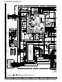
CD-C606/1900,CP-C606/1900
SERVICE MANUAL
No. S3909CDC606//
CD-C606
CD-C1900
CP-C606
CP-C1900
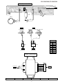
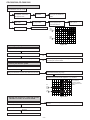
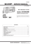
Illustration: CD-C606
CD-C606 mini component system consisting of
CD-C606 mini component system and
CP-C606 speaker system
CD-C1900 mini component system consisting of
CD-C1900 mini component system and
CP-C1900 speaker system
• In the interests of user-safety the set should be restored to its
original condition and only parts identical to those specified be
used.
CONTENTS
Page
IMPORTANT SERVICE NOTES (FOR U.S.A. ONLY) ....................................................................................................... 2
SPECIFICATIONS ............................................................................................................................................................. 2
NAMES OF PARTS ........................................................................................................................................................... 3
OPERATION MANUAL ...................................................................................................................................................... 5
QUICK GUIDE ................................................................................................................................................................... 6
DISASSEMBLY .................................................................................................................................................................. 8
REMOVING AND REINSTALLING THE MAIN PARTS ................................................................................................... 10
ADJUSTMENT ................................................................................................................................................................. 11
NOTES ON SCHEMATIC DIAGRAM .............................................................................................................................. 13
TYPE OF TRANSISTER AND LED ................................................................................................................................. 13
WAVEFORMS OF CD CIRCUIT ...................................................................................................................................... 14
BLOCK DIAGRAM ........................................................................................................................................................... 15
SCHEMATIC DIAGRAM / WIRING SIDE OF P.W.BOARD .............................................................................................. 18
VOLTAGE ........................................................................................................................................................................ 32
TROUBLESHOOTING ..................................................................................................................................................... 33
FUNCTION TABLE OF IC ................................................................................................................................................ 37
FL SEGMENT ................................................................................................................................................................... 42
PARTS GUIDE/EXPLODED VIEW
PACKING OF THE SET (FOR U.S.A. ONLY)
SHARP CORPORATION
–1–
This document has been published to be used
for after sales service only.
The contents are subject to change without notice.
CD-C606/1900,CP-C606/1900
FOR A COMPLETE DESCRIPTION OF THE OPERATION OF THIS UNIT, PLEASE REFER
TO THE OPERATION MANUAL.
IMPORTANT SERVICE NOTES (FOR U.S.A. ONLY)
BEFORE RETURNING THE AUDIO PRODUCT
(Fire & Shock Hazard)
Before returning the audio product to the user, perform the
following safety checks.
1. Inspect all lead dress to make certain that leads are not
pinched or that hardware is not lodged between the chassis
and other metal parts in the audio product.
2. Inspect all protective devices such as insulating materials,
cabinet, terminal board, adjustment and compartment
covers or shields, mechanical insulators etc.
3. To be sure that no shock hazard exists, check for leakage
current in the following manner.
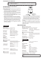
* Plug the AC line cord directly into a 120 volt AC outlet.
* Using two clip leads, connect a 1.5k ohm, 10 watt resistor
paralleled by a 0.15µF capacitor in series with all exposed
metal cabinet parts and a known earth ground, such as
conduit or electrical ground connected to earth ground.
* Use a VTVM or VOM with 1000 ohm per volt, or higher,
sensitivity to measure the AC voltage drop across the
resistor (See diagram).
1.5k ohms
10W
0.15µF
TEST PROBE
TO EXPOSED
METAL PARTS
CONNECT TO
KNOWN EARTH
GROUND
* Connect the resistor connection to all exposed metal parts
having a return path to the chassis (antenna, metal cabinet,
screw heads, knobs and control shafts, escutcheon, etc.)
and measure the AC voltage drop across the resistor.
All check must be repeated with the AC line cord plug connection
reversed.
Any reading of 0.3 volt RMS (this corresponds to 0.2 milliamp.
AC.) or more is excessive and indicates a potential shock
hazard which must be corrected before returning the audio
product to the owner.
SPECIFICATIONS
CD-C606/1900
● Cassette deck section
● General
Power source:
VTVM
AC SCALE
AC 120 V, 60 Hz
Frequency response: 50-14,000 Hz (Normal tape)
Power consumption: Stand-by; 0.3 W
Power on; 40 W
Signal/noise ratio:
55 dB (TAPE 1, playback)
50 dB (TAPE 2, recording/playback)
Dimensions:
(For U.S.A.)
Wow and flutter:
0.15 % (WRMS)
Dimensions:
(For Canada)
Weight:
(For U.S.A.)
Weight:
(For Canada)
Width; 10-5/8" (270 mm)
Height; 11-13/16" (300 mm)
Depth; 13-7/8" (353 mm)
Width; 270 mm (10-5/8")
Height; 300 mm (11-13/16")
Depth; 353 mm (13-7/8")
10.3 lbs (4.7 kg)
4.7 kg (10.3 lbs)
● Compact disc player section
Type:
Signal readout:
D/A converter:
1-bit D/A converter
Frequency response: 20 -20,000 Hz
Dynamic range:
Output power:
(For Canada)
Output terminals:
10 watts minimum RMS per
channel into 8 ohms from 80 Hz to
20 kHz, 10% total harmonic
distortion
MPO; 36 W (18 W + 18 W)
(10% T.H.D.)
RMS; 20 W (10 W + 10 W)
(10% T.H.D.)
Speakers; 8 ohms
Headphones; 16-50 ohms
(recommended; 32 ohms)
● Speaker section
Type:
2-way [4” (10cm) woofer and
super tweeter]
Maximum input
power:
20 W
Rated input power:
10 W
Impedance:
8 ohms
Dimensions:
(For U.S.A.)
Width; 8-11/16" (220 mm)
Height; 11-13/16" (300 mm)
Depth; 7-1/16" (180 mm)
Dimensions:
(For Canada)
Width; 220 mm (8-11/16")
Height; 300 mm (11-13/16")
Depth; 180 mm (7-1/16")
Weight:(For U.S.A.) 4.4 lbs. (2.0 kg)/each
Weight:(For Canada) 2.0 kg (4.4 lbs.)/each
● Tuner section
Frequency range:
90 dB (1 kHz)
CP-C606/1900
● Amplifier section
Output power:
(For U.S.A.)
3-disc multi-play compact disc player
Non-contact, 3-beam semiconductor
laser pickup
FM; 87.5-108 MHz
AM; 530-1,720 kHz
Specifications for this model are subject to change without prior
notice.
–2–
CD-C606/1900,CP-C606/1900
FOR A COMPLETE DESCRIPTION OF THE OPERATION OF THIS UNIT, PLEASE REFER
TO THE OPERATION MANUAL.
IMPORTANT SERVICE NOTES (FOR U.S.A. ONLY)
BEFORE RETURNING THE AUDIO PRODUCT
(Fire & Shock Hazard)
Before returning the audio product to the user, perform the
following safety checks.
1. Inspect all lead dress to make certain that leads are not
pinched or that hardware is not lodged between the chassis
and other metal parts in the audio product.
2. Inspect all protective devices such as insulating materials,
cabinet, terminal board, adjustment and compartment
covers or shields, mechanical insulators etc.
3. To be sure that no shock hazard exists, check for leakage
current in the following manner.
* Plug the AC line cord directly into a 120 volt AC outlet.
* Using two clip leads, connect a 1.5k ohm, 10 watt resistor
paralleled by a 0.15µF capacitor in series with all exposed
metal cabinet parts and a known earth ground, such as
conduit or electrical ground connected to earth ground.
* Use a VTVM or VOM with 1000 ohm per volt, or higher,
sensitivity to measure the AC voltage drop across the
resistor (See diagram).
1.5k ohms
10W
0.15µF
TEST PROBE
TO EXPOSED
METAL PARTS
CONNECT TO
KNOWN EARTH
GROUND
* Connect the resistor connection to all exposed metal parts
having a return path to the chassis (antenna, metal cabinet,
screw heads, knobs and control shafts, escutcheon, etc.)
and measure the AC voltage drop across the resistor.
All check must be repeated with the AC line cord plug connection
reversed.
Any reading of 0.3 volt RMS (this corresponds to 0.2 milliamp.
AC.) or more is excessive and indicates a potential shock
hazard which must be corrected before returning the audio
product to the owner.
SPECIFICATIONS
CD-C606/1900
● Cassette deck section
● General
Power source:
VTVM
AC SCALE
AC 120 V, 60 Hz
Frequency response: 50-14,000 Hz (Normal tape)
Power consumption: Stand-by; 0.3 W
Power on; 40 W
Signal/noise ratio:
55 dB (TAPE 1, playback)
50 dB (TAPE 2, recording/playback)
Dimensions:
(For U.S.A.)
Wow and flutter:
0.15 % (WRMS)
Dimensions:
(For Canada)
Weight:
(For U.S.A.)
Weight:
(For Canada)
Width; 10-5/8" (270 mm)
Height; 11-13/16" (300 mm)
Depth; 13-7/8" (353 mm)
Width; 270 mm (10-5/8")
Height; 300 mm (11-13/16")
Depth; 353 mm (13-7/8")
10.3 lbs (4.7 kg)
4.7 kg (10.3 lbs)
● Compact disc player section
Type:
Signal readout:
D/A converter:
1-bit D/A converter
Frequency response: 20 -20,000 Hz
Dynamic range:
Output power:
(For Canada)
Output terminals:
10 watts minimum RMS per
channel into 8 ohms from 80 Hz to
20 kHz, 10% total harmonic
distortion
MPO; 36 W (18 W + 18 W)
(10% T.H.D.)
RMS; 20 W (10 W + 10 W)
(10% T.H.D.)
Speakers; 8 ohms
Headphones; 16-50 ohms
(recommended; 32 ohms)
● Speaker section
Type:
2-way [4” (10cm) woofer and
super tweeter]
Maximum input
power:
20 W
Rated input power:
10 W
Impedance:
8 ohms
Dimensions:
(For U.S.A.)
Width; 8-11/16" (220 mm)
Height; 11-13/16" (300 mm)
Depth; 7-1/16" (180 mm)
Dimensions:
(For Canada)
Width; 220 mm (8-11/16")
Height; 300 mm (11-13/16")
Depth; 180 mm (7-1/16")
Weight:(For U.S.A.) 4.4 lbs. (2.0 kg)/each
Weight:(For Canada) 2.0 kg (4.4 lbs.)/each
● Tuner section
Frequency range:
90 dB (1 kHz)
CP-C606/1900
● Amplifier section
Output power:
(For U.S.A.)
3-disc multi-play compact disc player
Non-contact, 3-beam semiconductor
laser pickup
FM; 87.5-108 MHz
AM; 530-1,720 kHz
Specifications for this model are subject to change without prior
notice.
–2–
CD-C606/1900,CP-C606/1900
CD-C606/1900
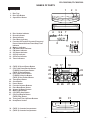
NAMES OF PARTS
■ Front panel
2
1
3
1. Disc Tray
2. Disc Skip Button
3. Open/Close Button
4.
5.
6.
7.
8.
9.
10.
11.
12.
13.
14.
15.
4
Disc Number Indicator
Record Indicator
Sleep Indicator
Extra Bass Indicator
Function/CD Track/CD Counter/Frequency/
Preset Channel/Volume/Timer/Sleep Time
Indicator
Memory Indicator
FM Stereo Mode Indicator
FM Stereo Indicator
CD Repeat Indicator
CD Play Indicator
CD Pause Indicator
Timer Indicators
1
2
3
56
7
REC SLEEP
X-BASS
9 10 11
8
MEMORY ST
12
kHz
MHz
13 14 15
16 17
16. (TAPE 2) Record Pause Button
17. (CD) Track Down/Review Button
(TUNER) Preset Down Button
(TAPE 2) Rewind Button
18. (CD) Track Up/Cue Button
(TUNER) Preset Up Button
(TAPE 2) Fast Foward Button
19. Timer/Sleep Button
20. Clock Button
21. Power Button
22. Function Selector Buttons
23. Extra Bass/Demo Button
24. Volume Up/Down Buttons
25. Memory/Set Button
26. (CD/TAPE) Stop Button
27. (CD) Play/Repeat Button
(TAPE) Play Button
28. Tuning and Time Up/Down Buttons
29. Headphone Socket
18
19
20
21
23
24
22
25 26
30
30. (TAPE 1) Cassette Compartment
31. (TAPE 2) Cassette Compartment
–3–
27 28
31
29
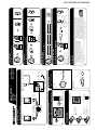
CD-C606/1900,CP-C606/1900
CD-C606/1900
■ Rear panel
1. AC Power Input Socket
2. Speaker Terminals
3. FM/AM Loop Aerial Socket
3
1
2
CP-C606/1900
■ Speaker
4.
5.
6.
7.
Super Tweeter
Woofer
Bass Reflex Duct
Speaker Wire
4
5
6
7
CD-C606/1900
■ Remote control
1. Remote Control Transmitter LED
1
● CD control section
2.
3.
4.
5.
6.
7.
8.
9.
10.
11.
Disc Number Select Buttons
Memory Button
Pause Button
Clear Button
Track Down/Review Button
Track Up/Cue Button
Disc Skip Button
Play/Repeat Button
Stop Button
Random Button
● Tuner control section
2
8
3
9
4
5
6
7
10
11
12
13
12. Preset Up/Down Buttons
● Tape control section
13.
14.
15.
16.
17.
18.
19.
20.
21.
22.
14 15 16 17
1
18
19
20
21
(TAPE 1) Play Button
(TAPE 1/2) Stop Button
(TAPE 2) Play Button
(TAPE 2) Rewind Button
(TAPE 2) Fast Forward Button
(TAPE 2) Record Pause Button
Function Selector Buttons
Power Button
Extra Bass Button
Volume Up/Down Buttons
–4–
22
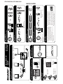
–5–
9
8
7
6
5
4
3
2
AM 12:00
MEMORY/
SET
POWER
CLOCK
AM 0:00
0:00
TUNING/
TIME
(
)
(Main unit operation)
In this example, the clock is set for the 12-hour
(AM 12:00) system.
SETTING THE CLOCK
or
) button to adjust the hour.
or
) button to adjust the minutes.
2 Perform steps 1 - 9 above.
COMPUTER".
1 Perform steps 1 - 2 in the section "RESETTING THE MICRO
To change the time display mode:
The time display will appear for about 5 seconds.
Press the CLOCK button.
To see the time display:
3 Perform steps 6 - 9 above.
2 Within 5 seconds, press the MEMORY/SET button.
1 Press the CLOCK button.
To change the clock time:
The clock starts operating from "0" seconds. (Seconds are not
displayed.)
Note:
In the event of power failure or when the AC power cord is
disconnected, the clock display will go out.
When the AC power supply is restored, the clock display will
flash on and off to indicate the time when the power failure
occurred or when the AC power cord was disconnected.
If this happens, follow the procedure below to change the clock
time.
9 Press the MEMORY/SET button.
Press the TUNING/TIME ( or ) button once to advance
the time by 1 minute. Hold it down to change the time in 5
minute intervals.
The hour setting will not advance even if minutes advance
from "59" to "00".
7
8 Press the TUNING/TIME (
Press the TUNING/TIME ( or ) button once to advance
the time by 1 hour. Hold it down to advance continuously.
When the 12-hour display is selected, "AM" will change automatically to "PM".
Press the MEMORY/SET button.
5
6 Press the TUNING/TIME (
The 12-hour display will appear.
(AM 12:00 - PM 11:59)
"AM 0:00"
The 12-hour display will appear.
(AM 0:00 - PM 11:59)
"0:00"
The 24-hour display will appear.
(0:00 - 23:59)
Note that this can only be set when the unit is first installed or
it has been reset (see page 13).
Press the MEMORY/SET button.
"AM 12:00"
display mode.
1 Press the POWER button to enter the stand-by mode.
2 Press the CLOCK button.
3 Within 5 seconds, press the MEMORY/SET button.
4 Press the TUNING/TIME ( or ) button to select the time
15
1
15
1,2
2
RESETTING THE MICROCOMPUTER
8" - 20'
(0.2 m - 6 m)
PREPARATION FOR USE
Caution:
● The operation explained above will erase all data stored in
memory including clock and timer settings, and tuner and CD
preset.
/
button, hold down the POWER button for at least 1 second.
1 Press the POWER button to enter the stand-by mode.
2 Press and hold down the / button and the
● If the operation is not correct.
● If the display is not correct.
Reset the microcomputer under the following conditions:
● To erase all of the stored memory contents (clock and timer
settings, and tuner and CD presets).
● Keep the remote control away from moisture, excessive heat,
shock, and vibrations.
● Exposing the sensor on the main unit to strong light may interfere with operation. Change the lighting or the direction of the
unit.
● Periodically clean the transmitter LED on the remote
control and the sensor on the main unit with a soft cloth.
Notes concerning use:
● Replace the batteries if the operating distance is reduced or if
the operation becomes erratic.
■ Remote control
CD-C606/1900,CP-C606/1900
OPERATION MANUAL
RIGHT
LEFT
SPEAKERS
RATED SPEAKER IMPEDANCE:
8 OHMS MIN.
Red
Rojo
Black
Negro
Left speaker
Altavoz izquierdo
–6–
● Batteries are not
included.
● Las pilas no están
incluidas.
15
1
15
8" - 20' (0.2m - 6m)
0,2m - 6m
X-BASS /DEMO
● Extra-BASS
● Graves extra
VOLUME
X-BASS
VOLUME
FM STERO
CD
TAPE 2
ST
FM MONO
TAPE 2
TUNING
/TIME
● CD recording starts.
● La grabación de CD
empieza.
OPEN
/CLOSE
● El nivel de sonido en una posición de volumen
fijado depende de una combinación del
rendimiento de las altavoces, la posición y
muchos otros factores. Es aconsejable evitar un
aumento de volumen. Esto se produce, por
ejemplo, al conectar el aparato con el volumen
puesto en una posición alta. Evite continuar la
audición prolongada a altos niveles de sonido.
● En este aparato sólo pueden reproducirse los
discos que tengan el logotipo mostrado.
REC PAUSE
AM
● Label facing up
● Etiqueta hacia arriba
● The sound level at a given volume setting
depends on a combination of speaker efficiency,
location and many other factors. It is advisable
to avoid exposure to high volume levels, which
occur while turning the unit on with the volume
control setting up high, or while continually
listening at high volume levels.
● Only discs bearing the logo as shown can be
played in this unit.
Precaution
Precaución
● Load the disc to be
recorded.
● Introduzca el disco que
va a grabar.
PE )
2
● 2 “AA” batteries
● Dos pilas “AA”
Remote Sensor
Sensor remote
1
OPEN
/CLOSE
Recording from CDs
Grabación de discos compactos
CD
TA
(1
Remote control
Control remoto
POWER
CD
Radio operation
Funcionamiento de la radio
PE )
2
● Volume
● Volumen
TAPE 1
CD playback
Reproducción de discos compactos
TA
(1
POWER
● AC 120 V, 60 Hz
● 120 V de CA, 60 Hz
● FM Antenna
● Antena de FM
Sound control
Control del sonido
● AM Loop Antenna
● Antena de cuadro de
AM
PE )
2
Turning the power on and off
Conexión y desconexión de la alimentación
Black
Negro
Red
Rojo
Right speaker
Altavoz derecho
Preparation for use
Preparación para su uso
CD
TU
(B NER
AN
D)
CD-C606
TU
(B NER
AN
D)
Tape playback
Reproducción de cintas
TA
(1
TU
(B NER
AN
D)
Quick-Guide
Guía rápida
PE
TA 2)
(1
TU
(B NER
AN
D)
MINI COMPONENT
SYSTEM
CD-C606/1900,CP-C606/1900
QUICK GUIDE
Rojo
Red
RIGHT
LEFT
SPEAKERS
RATED SPEAKER IMPEDANCE:
8 OHMS MIN.
Rojo
Red
Black
Negro
Left speaker
Altavoz izquierdo
–7–
● Batteries are not
included.
● Las pilas no están
incluidas.
15
1
15
8" - 20' (0.2m - 6m)
0,2m - 6m
X-BASS /DEMO
● Extra-BASS
● Graves extra
VOLUME
X-BASS
VOLUME
FM STERO
CD
TAPE 2
ST
FM MONO
TAPE 2
● Only discs bearing the logo as shown can be
played in this unit.
TUNING
/TIME
● CD recording starts.
● La grabación de CD
empieza.
OPEN
/CLOSE
● El nivel de sonido en una posición de volumen
fijado depende de una combinación del
rendimiento de las altavoces, la posición y
muchos otros factores. Es aconsejable evitar un
aumento de volumen. Esto se produce, por
ejemplo, al conectar el aparato con el volumen
puesto en una posición alta. Evite continuar la
audición prolongada a altos niveles de sonido.
● En este aparato sólo pueden reproducirse los
discos que tengan el logotipo mostrado.
REC PAUSE
AM
● Label facing up
● Etiqueta hacia arriba
● The sound level at a given volume setting
depends on a combination of speaker efficiency,
location and many other factors. It is advisable
to avoid exposure to high volume levels, which
occur while turning the unit on with the volume
control setting up high, or while continually
listening at high volume levels.
Precaution
Precaución
● Load the disc to be
recorded.
● Introduzca el disco que
va a grabar.
PE )
2
● 2 “AA” batteries
● Dos pilas “AA”
Remote Sensor
Sensor remote
1
OPEN
/CLOSE
Recording from CDs
Grabación de discos compactos
CD
TA
(1
Remote control
Control remoto
POWER
CD
Radio operation
Funcionamiento de la radio
PE )
2
● Volume
● Volumen
TAPE 1
CD playback
Reproducción de discos compactos
TA
(1
POWER
● AC 120 V, 60 Hz
● 120 V de CA, 60 Hz
● FM Antenna
● Antena de FM
PE )
2
Sound control
Control del sonido
● AM Loop Antenna
● Antena de cuadro de
AM
TA
(1
Turning the power on and off
Conexión y desconexión de la alimentación
Black
Negro
Right speaker
Altavoz derecho
Preparation for use
Preparación para su uso
CD
TU
(B NER
AN
D)
CD-C1900
TU
(B NER
AN
D)
Tape playback
Reproducción de cintas
PE )
2
TU
(B NER
AN
D)
Quick-Guide
Guía rápida
TA
(1
TU
(B NER
AN
D)
MINI COMPONENT
SYSTEM
CD-C606/1900,CP-C606/1900
RIGHT
LEFT
SPEAKERS
RATED SPEAKER IMPEDANCE:
8 OHMS MIN.
Red
Rojo
Black
Negro
Left speaker
Altavoz izquierdo
–6–
● Batteries are not
included.
● Las pilas no están
incluidas.
15
1
15
8" - 20' (0.2m - 6m)
0,2m - 6m
X-BASS /DEMO
● Extra-BASS
● Graves extra
VOLUME
X-BASS
VOLUME
FM STERO
CD
TAPE 2
ST
FM MONO
TAPE 2
TUNING
/TIME
● CD recording starts.
● La grabación de CD
empieza.
OPEN
/CLOSE
● El nivel de sonido en una posición de volumen
fijado depende de una combinación del
rendimiento de las altavoces, la posición y
muchos otros factores. Es aconsejable evitar un
aumento de volumen. Esto se produce, por
ejemplo, al conectar el aparato con el volumen
puesto en una posición alta. Evite continuar la
audición prolongada a altos niveles de sonido.
● En este aparato sólo pueden reproducirse los
discos que tengan el logotipo mostrado.
REC PAUSE
AM
● Label facing up
● Etiqueta hacia arriba
● The sound level at a given volume setting
depends on a combination of speaker efficiency,
location and many other factors. It is advisable
to avoid exposure to high volume levels, which
occur while turning the unit on with the volume
control setting up high, or while continually
listening at high volume levels.
● Only discs bearing the logo as shown can be
played in this unit.
Precaution
Precaución
● Load the disc to be
recorded.
● Introduzca el disco que
va a grabar.
PE )
2
● 2 “AA” batteries
● Dos pilas “AA”
Remote Sensor
Sensor remote
1
OPEN
/CLOSE
Recording from CDs
Grabación de discos compactos
CD
TA
(1
Remote control
Control remoto
POWER
CD
Radio operation
Funcionamiento de la radio
PE )
2
● Volume
● Volumen
TAPE 1
CD playback
Reproducción de discos compactos
TA
(1
POWER
● AC 120 V, 60 Hz
● 120 V de CA, 60 Hz
● FM Antenna
● Antena de FM
Sound control
Control del sonido
● AM Loop Antenna
● Antena de cuadro de
AM
PE )
2
Turning the power on and off
Conexión y desconexión de la alimentación
Black
Negro
Red
Rojo
Right speaker
Altavoz derecho
Preparation for use
Preparación para su uso
CD
TU
(B NER
AN
D)
CD-C606
TU
(B NER
AN
D)
Tape playback
Reproducción de cintas
TA
(1
TU
(B NER
AN
D)
Quick-Guide
Guía rápida
PE
TA 2)
(1
TU
(B NER
AN
D)
MINI COMPONENT
SYSTEM
CD-C606/1900,CP-C606/1900
QUICK GUIDE
Rojo
Red
RIGHT
LEFT
SPEAKERS
RATED SPEAKER IMPEDANCE:
8 OHMS MIN.
Rojo
Red
Black
Negro
Left speaker
Altavoz izquierdo
–7–
● Batteries are not
included.
● Las pilas no están
incluidas.
15
1
15
8" - 20' (0.2m - 6m)
0,2m - 6m
X-BASS /DEMO
● Extra-BASS
● Graves extra
VOLUME
X-BASS
VOLUME
FM STERO
CD
TAPE 2
ST
FM MONO
TAPE 2
● Only discs bearing the logo as shown can be
played in this unit.
TUNING
/TIME
● CD recording starts.
● La grabación de CD
empieza.
OPEN
/CLOSE
● El nivel de sonido en una posición de volumen
fijado depende de una combinación del
rendimiento de las altavoces, la posición y
muchos otros factores. Es aconsejable evitar un
aumento de volumen. Esto se produce, por
ejemplo, al conectar el aparato con el volumen
puesto en una posición alta. Evite continuar la
audición prolongada a altos niveles de sonido.
● En este aparato sólo pueden reproducirse los
discos que tengan el logotipo mostrado.
REC PAUSE
AM
● Label facing up
● Etiqueta hacia arriba
● The sound level at a given volume setting
depends on a combination of speaker efficiency,
location and many other factors. It is advisable
to avoid exposure to high volume levels, which
occur while turning the unit on with the volume
control setting up high, or while continually
listening at high volume levels.
Precaution
Precaución
● Load the disc to be
recorded.
● Introduzca el disco que
va a grabar.
PE )
2
● 2 “AA” batteries
● Dos pilas “AA”
Remote Sensor
Sensor remote
1
OPEN
/CLOSE
Recording from CDs
Grabación de discos compactos
CD
TA
(1
Remote control
Control remoto
POWER
CD
Radio operation
Funcionamiento de la radio
PE )
2
● Volume
● Volumen
TAPE 1
CD playback
Reproducción de discos compactos
TA
(1
POWER
● AC 120 V, 60 Hz
● 120 V de CA, 60 Hz
● FM Antenna
● Antena de FM
PE )
2
Sound control
Control del sonido
● AM Loop Antenna
● Antena de cuadro de
AM
TA
(1
Turning the power on and off
Conexión y desconexión de la alimentación
Black
Negro
Right speaker
Altavoz derecho
Preparation for use
Preparación para su uso
CD
TU
(B NER
AN
D)
CD-C1900
TU
(B NER
AN
D)
Tape playback
Reproducción de cintas
PE )
2
TU
(B NER
AN
D)
Quick-Guide
Guía rápida
TA
(1
TU
(B NER
AN
D)
MINI COMPONENT
SYSTEM
CD-C606/1900,CP-C606/1900
CD-C606/1900,CP-C606/1900
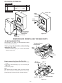
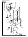
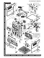
CP-C606/1900
STEP
1
PROCEDURE
REMOVAL
Speaker
FIGURE
1. Net .......................... (A1) x1
2. Duct Panel .............. (A2) x1
3. Screw ...................... (A3) x4
CP-C606/1900
10-1
10-2
Speaker Box
Speaker Box
Super
Tweeter
Woofer
(A1)x1
(A2)x1
(A3)x4
ø3.5x13mm
Driver
Driver should be
pried away from
Speaker Box.
Direction of handle
Figure 10-2
Figure 10-1
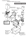
REMOVING AND REINSTALLING THE MAIN PARTS
CD MECHANISM SECTION
Perform steps 1, 2, 3, and 8 ~ 12 of the disassembly method
to remove the CD mechanism.
How to remove the turntable up/down/loading
motor (See Fig. 10-3)
1. Remove the screws (A1) x 2 pcs., to remove the turntable
up/down/loading motor.
Turntable Up/Down/
Loading Motor
Motor
PWB
(A1) x2
ø2.6 x5mm
Figure 10-3
How to remove the pickup (See Fig. 10-4)
1. Remove the screws (B1) x 2 pcs., to remove the shaft (B2)
x 1 pc.
2. Remove the stop washer (B3) x 1 pc., to remove the gear
(B4) x 1 pc.
3. Remove the pickup.
(B1) x2
ø2.6 x6mm
(B3) x1
Note:
After disconnecting the optical pickup connector wrap the
front end of connector in conductive aluminum foil so as to
prevent damage to the optical pickup by static electricity.
Pickup
(B2) x1
CD Mechanism
(B4) x1
Figure 10-4
– 10 –
CD-C606/1900,CP-C606/1900
ADJUSTMENT
MECHANISM SECTION
TUNER SECTION
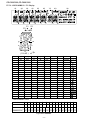
• Driving Force Check
fL: Low-range frequency
fH: High-renge frequency
• AM IF/RF
Signal generator: 400 Hz, 30%, AM modulated
Torque Meter
Specified Value
Play: TW-2412
Tape 1: Over 80 g
Tape 2: Over 80 g
Test Stage Frequency
Frequency
Display
IF
450 kHz
1,720 kHz
Band
Coverage
—
530 kHz
(fL): T333 *2
1.1 ± 0.1 V
Tracking
990 kHz
990 kHz
(fL): T331
• Torque Check
Torque Meter
Specified Value
Tape 1
Play: TW-2111
Tape 2
30 to 60 g. cm
30 to 60 g.cm
Fast forward: TW-2231
—
60 to 120 g.cm
Rewind: TW-2231
—
60 to 120 g.cm
Adjusting
Point
Specified
Value
Normal
speed
MTT-111
Volume in
motor
(MM1)
3,000 ±
30 Hz
*1
*1. Input: Antenna (CNP301), Output: TP301
*2. Input: Antenna (CNP301), Output: TP302
• Tape Speed
Test Tape
Setting/ Instrument
Adjusting Connection
Parts
T382
*1
• FM RF
Signal generator: 1 kHz, 22.5 kHz dev., FM modulated
Instrument
Connection
Test Stage Frequency Frequency
Display
Speaker
terminal
(Load
resistance:
8 ohms)
Serring/
Adjusting
Point
Band
Coverage
—
RF
98.00 MHz 98.00 MHz L312
(10-30 dB)
Instrument
Connection
87.50 MHz T301(fL):
3.4 V ± 50 mV
*1
*2
*1. Input: Antenna (CNP301), Output: TP302
*2. Input: Antenna (CNP301), Output: Speaker terminal
TAPE MECHANISM
• FM Detection
Signal generator: 10.7 MHz, FM sweep generator
Test
Stage
MM 1
Motor
Frequency Frequency
Display
Adjusting
Parts
Instrument
Connection
Detection 10.7 MHz
98.00 MHz
T381
Input: Pin 1 of
IC303
Output: TP302
IF
98.00 MHz
T302(Turn Input: Pin 1 of
the core of IC301
transformer Output: TP302
T381 fully
counterclookwise.)
Volume in motor
10.7 MHz
Figure 11-1 ADJUSTMENT POINTS
• VCO Frequency
9
1
11
FM Band
Coverage
fL
IC302
12
22
C354
FM IF
T301
TP301
1
T302
98.00 MHz
(60 dB)
BF301
L312
AM IF
AM Tracking
fL
1
CNP301
AM LOOP
ANTENNA
CF301
IC303
13
VR381 TP302
24
T381
FM DET
VR381*
Instrument
Connection
Pin 13, Pin 21
and ground
of IC303
Notes:
After preparing the test circuit shown in Fig 11-3, connect the
Pin 13 , Pin 21 and ground of the IC303 with test circuit, and
measure the Value.
At this time, apply a standard unmodulated signal input and
adjust the VCO.
Pin 13 of IC303
21
C386
98.00 MHz
Adjusting
Parts
* Adjust for 76 kHz ± 200 Hz.
FM RF
CF351 T382
12
Frequency
Display
Frequency
IC301
Pin 21 of IC303
T331
T333
G
AM Band
Coverage fL
D
FET : 2SK19 or 2SK54
TO FREQUENCY
COUNTER
S
VCO
10 kΩ
MAIN PWB
Figure 11-3
Figure 11-2 ADJUSTMENT POINTS
– 11 –
CD-C606/1900,CP-C606/1900
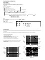
TEST MODE
• Setting the test mode
Any one of test mode can be set by pressing several keys as follows.
<REC. PAUSE> + <DISC. SKIP> + <POWER>
TEST: CD operation test
• TEST mode
Function — CD test mode
Setting of TEST mode
Indication of CD TST mode (Fig. 12-1)
IL is not performed.
OPEN/CLOSE operation is manual operation.
The pickup can be moved by using the (
<MEMORY>
LASER ON
<MEMORY>
Tracking on the spot.
SERVO OFF PLAY
<PLAY> key input
) or (
) key.
<MEMORY>
Tracking on the spot.
SERVO ON PLAY
<STOP>
STOP
TOC. IL is performed, and the ordinary PLAY is performed.
If the following key is pressed during PLAY, it is possible
to specify directly any Track No.
<Disc Number 1> key: Track 4
<Disc Number 2> key: Track 9
<Disc Number 3> key: Track 15
Note:
Only in STOP state it is possible to slide the pickup with the (
VOL. --- Last memory
BAL. --- CENTER
R.GEQ. --- FLAT
X-BAS --- OFF
1
) or (
2
Press <STOP> key.
Stop
) key.
3
Canceling method - POWER OFF
Figure 12-1
CD SECTION
Since this CD system incorporates the following automatic adjustment function, when the pickup is replaced, it is not necessary
to readjust it.
Since this CD unit does not need adjustment, the combination of PWB and laser pickup unit is not restricted.
• Automatic adjustment item
1. Focus offset (Fig. 12-2)
2. Tracking offset (Fig. 12-3)
3. E/F balance (tracking error balance) (Fig. 12-4)
4. RF level AGC function (HF level: constant)
5. RF level automatic follow-up of the tracking gain
0.1s
0.50 V
IC1 20 FE
This automatic adjustment is performed each time a disc is
changed. Therefore, each disc is played back using the
optimal settings.
0.1s
0.50 V
IC1 7 TE
FOCUS
OFF-SET
ADJUST
TRACKING
OFF-SET
1 ADJUST
2
Figure 12-2
Enlarged
View
10ms
0.50 V
IC1 20 FE
TRACKING/
ERROR
BARANCE
1 ADJUST
200 ms
1V/diV
IC 1 15
TO
10ms
0.50 V
IC1 7 TE
200 ms
1V/diV
IC 1 7
TE
TRACKING
OFF-SET
1 ADJUST
2
2
Figure 12-3
Figure 12-4
– 12 –
CD-C606/1900,CP-C606/1900
NOTES ON SCHEMATIC DIAGRAM
• Resistor:
To differentiate the units of resistors, such symbol as K and
M are used: the symbol K means 1000 ohm and the symbol
M means 1000 kohm and the resistor without any symbol is
ohm-type resistor. Besides, the one with “Fusible” is a fuse
type.
• Capacitor:
To indicate the unit of capacitor, a symbol P is used: this
symbol P means micro-micro-farad and the unit of the
capacitor without such a symbol is microfarad. As to
electrolytic capacitor, the expression “capacitance/withstand
voltage” is used.
(CH), (TH), (RH), (UJ): Temperature compensation
(ML): Mylar type
(P.P.): Polypropylene type
• Schematic diagram and Wiring Side of P.W.Board for this
model are subject to change for improvement without prior
notice.
REF. NO
DESCRIPTION
• The indicated voltage in each section is the one measured
by Digital Multimeter between such a section and the chassis with no signal given.
1. In the tuner section,
( ) indicates AM
< > indicates FM stereo
2. In the main section, a tape is being played back.
3. In the deck section, a tape is being played back.
( ) indicates the record state.
4. In the power section, a tape is being played back.
5. In the CD section, the CD is stopped.
• Parts marked with “
”(
) are important for
maintaining the safety of the set. Be sure to replace these
parts with specified ones for maintaining the safety and
performance of the set.
POSITION
REF. NO
DESCRIPTION
POSITION
SW1
OPEN/CLOSE
ON—OFF
SW705
FAST FORWARD
ON—OFF
SW2
MECHA UP
ON—OFF
SW706
REWIND
ON—OFF
SW3
DISC NUMBER
ON—OFF
SW707
OPEN/CLOSE
ON—OFF
SW4
PICKUP IN
ON—OFF
SW708
STOP
ON—OFF
SW605
TAPE 1 MAIN
ON—OFF
SW709
DISC SKIP
ON—OFF
SW606
TAPE 2 MAIN
ON—OFF
SW710
X-BASS
ON—OFF
SW607
TAPE 1 RECORD
ON—OFF
SW711
FUNCTION
ON—OFF
SW608
TAPE 1 PLAY
ON—OFF
SW712
BAND
ON—OFF
SW701
POWER
ON—OFF
SW714
MEMORY
ON—OFF
SW702
VOLUME UP
ON—OFF
SW715
TUNING UP
ON—OFF
SW703
VOLUME DOWN
ON—OFF
SW716
TUNING DOWN
ON—OFF
SW704
PLAY
ON—OFF
FRONT
VIEW
FRONT
VIEW
FRONT
VIEW
E C B
(S)(G)(D)
(1) (2) (3)
2SC2389 SE
KRA102 M
KRA109 M
KRC102 M
KRC104 M
KRC107 M
KTA1266 GR
KTA1271 Y
KTA1273 Y
KTC3194 Y
KTC3199 GR
KTC3203 Y
B C E
(D)(G)(S)
(3) (2) (1)
1
2 3
SVC211C
SVC348S
2SA1318
Figure 13 TYPES OF TRANSISTOR AND LED
– 13 –
SLI342UCJ1
CD-C606/1900,CP-C606/1900
WAVEFORMS OF CD CIRCUIT
STOP
FOCUS
1
PLAY
SERCH
6
1
5ms
0.50 V
IC1 20 FE
7
1
8
1
12
5ms
5.0 V
IC1 54 DRF
9
1
3
0.5ms
10.0 V
IC1 33
0.5ms
10.0 V
IC1 32
0.5ms
0.50 V
IC1 14
0.5ms
1.00 V
IC1 7
JP+
JP-
JP
TE
1
CUE
3
1
0.5ms
1.00 V
IC1 41 HF
PLAY
20ms
V
10
1 1.00
IC1 27
4
1
0.5ms
5.0 V
IC1 4 HFL
5
1
0.5ms
5.0 V
IC1 36 TES
3
1
0.5ms
1.00 V
IC1 41 HF
4
1
0.5ms
5.0 V
IC1 4 HFL
5
1
0.5ms
5.0 V
IC1 36 TES
6
1
50ms
10.0 V
IC1 33 JP+
NORMAL DISC
TN0=01
SPO
1
2
3
20ms
V
11
1 2.00
IC2 12 CLV+
REVIEW
8
1
50ms
10.0 V
IC1 32 JP50ms
0.50 V
IC1 14 JP
9
1
50ms
1.00 V
IC1 7 TE
7
1
6
1
7
1
8
1
9
1
0.5ms
10.0 V
IC1 33
0.5ms
10.0 V
IC1 32
0.5ms
0.50 V
IC1 14
0.5ms
1.00 V
IC1 7
SPO
3
50ms
V
11
1 2.00
IC2 12 CLV+
CUE
PLAY
TCD-712
5s
100mV
IC1 29 SLD
JP+
JP-
JP
1
TE
8
1
9
1
50ms
1.00 V
IC1 7 TE
7
1
50ms
V
10
1 1.00
IC1 27
2
12
1
50ms
10.0 V
IC1 33 JP+
50ms
10.0 V
IC1 32 JP50ms
0.50 V
IC1 14 JP
6
1
PLAY TCD-712 (140mm)
TN0=01
1
REVIEW
12
1
0.5s
100mV
IC1 29 SLD
1
– 14 –
M
1 2 3 4 5 6 CNP11
+B1
9 8 7 6 5 4 3 2 1
GND (D)
MECHA UP
GND (D)
DISK NO.
OPEN/CLOSE
GND (D)
M–
M+
SOL–
SOL+
CNS10 10
+
–
TO DISPLAY
SECTION
SOLM2
SOLENOID
SW1
OPEN/CLOSE
M3
TURNTABLE
UP/DOWN
LOADING
MOTOR
SW2
MECHA UP
TO MAIN SECTION
(TO IC401)
SW3
DISC NUMBER
CD-C606/1900,CP-C606/1900
+7V
CNP10 10
9 8 7 6 5 4 3 2 1
SWITCHING
REGULATOR
~
58
CONT1
62 LD0
23
25
20
17
SLD 29
SP 23
SPO 27
FD 16
TO 15
2
1
FOCUS COIL
M2
SLED
MOTOR
TRACKING COIL
29
22
21
14
8
6 7 4 5
M1
SPINDLE
MOTOR
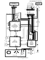
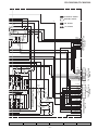
Figure 15 BLOCK DIAGRAM (1/3)
– 15 –
35
~
IC3
M63001FP
FOCUS/
TRACKING/
SPIN/SLED
DRIVER
1 2 3 4
PICKUP UNIT
PU-IN SW
+B5
+B1
SL+. SL–. DRF
42 41 20 40 24 18 28 39 38 37 36
DRF 54
SL+ 31
SL– 30
~
IC1
LA9241M
SERVO AMP.
CE 53
DAT 52
CL 51
CL, DAT, SELIAL CONTROL/CE
53
40 43 44
FIN2
FIN1
E
F
Q1
26
20
CV+
SLC
SL1
JP–
VOLTAGE
REGULATOR
+4.3V
64 VCC1
+5V
LASER DRIVER
32
~
Q52
CONT2
CONT4
LVSS
RVSS
LVDD
9 10 12
/RES. /CQCK. COIN
SQOUT. RWC. WRQ
45 XIN
CONT3
IC2
LC78622N
SERVO/SIGNAL
CONTROL
JP–
44 XOUT
24 25
EFMO
EFMIN
CLV+
XL1
16.93MHz
+5V
27
~
43 XVDD
41 RVDD
36 LVDD
23 VDD
5 ISET
6 VVDD
40 37 36 38 39
RCHO
LCHO
Q51
15 16 26 27
M
SW4
PICKUP IN
M
CD-C606/1900,CP-C606/1900
FM
ANTENNA
SWM3
FOOL PROOF
SWM4
F.A.S
SOLM1
SOLENOID
AM LOOP
ANTENNA
CNP301
1
2
3
BF301
1
IC301
TA7358AP
FM FRONT END
6
FM IF
AM IF
T302
1 CF301
+B4
+B4
3
SWM5
CAM
2
9
3
4
5
8
7
FM
OSC
L312
T301
1 CF351 3
T382
FM IF IN
FM OSC
FM RF
VR381
VCO
AM IF
T381
2
MONO/ST
FM DET
21
20
5
AM IF FM+B FM DET
1 3
AM MIX
15
13
VCO MO/ST
IC303
LA1805 FM IF DET./FM MPX./AM IF
7
11
STEREO
22
AM+B
OSC BUFF
L 9
R 10
FM/AM
23
AM RF IN
GND
24
6
FMOSC
Q301
AM OSC IN
FM/AM
SWITCHING
Q381
AM ANTENNA
AM OSC.
RESET
+B7
20
22
1
OSC
15
16
3
11
4
5
IC302
LC72131
PLL CONTROLLER
7
FM +B
1 IC702
2
3
DO
CL
CE
X352
4.5MHz
VT
DI
T333
FM IN
T331
AM IN
1
2
3
BAND PASS
FILTER
6
VOLTAGE
REGULATOR
+B4
VDD 17
21
10
FM
Q351
SWITCHING
+B4
11
TAPE
CNS401
FROM CD SECTION
CNP11
1
2
3
4
TAPE 1
TUNER
CD
IC501
AN7345K
PLAYBACK AND RECORD
/PLAYBACK AMP.
L(T1) 1
R(T1) 24
L-CH
R-CH
PLAYBACK
HEAD
REC
TAPE 2
P.B
L-CH
R-CH
RECORD/
PLAYBACK HEAD
AC BIAS
SWITCHING
Q504~Q509
P.B.
13
L(T2) 2
R(T2) 23
4 L
21 R
L NF 3
R NF 4
20
PB
5
T1/T2
L REC 9 REC
R REC 16
POP REDUCE 6
H/N
NOR/
HIGH
15
4
17
3
18
2
IC401
M62439SP
AUDIO PROCESSOR
13 R
8 L
19
1 20
9
Q514
Q515
Q512
Q513
R
SWITCHING
L REC
R
8 L NF
17 R NF
10 ALC
7
18
REF 14
12
+B4
L
R
L
R
L
R
10
T1/T2
19
T1
ERASE
HEAD
Figure 16 BLOCK DIAGRAM (2/3)
– 16 –
CD-C606/1900,CP-C606/1900
3
F
FL701
FL DISPLAY
Q701
M
Q702
MM1
TAPE MOTOR
3 ~ 14
1 2
17 21 ~ 30
31
32 33
Q703
MONO/ST
15
O/ST
L 9
R 10
71
54
51
50
49
1
1
2
3
4
5
6
44
42
43
52
47
41
40
39
38
37
36
81
SET
02
2
73 ~ 77 80
60 ~ 70 72 79
56 58
/AM
3
1
RX701 3
2
IC701
IX0282AW
SYSTEM MICROCOMPUTER
7
+B7
29
27 26 25
12 11 10 9
57 24 23 22 21 30 19 18 16 15 14 13 34 35 17
REMOTE
SENSOR
+B4
TO CD
SECTION
CNP12
RESET
+B5
KEY
SW701~SW703
SW707~SW722
PHM1 LED701
XL701
4.19MHz
Q704
+B5
+B4
JK601
HEADPHONES
Q631
Q632
SO601
SPEAKER
TERMINALS
3
13 R
2
5
8 L
OR
Q401
Q402
IC601
LA4282
POWER AMP.
+B
11 L-OUT
PT901
POWER
TRANSFORMER
12
10
+12V(MOTOR)
REC
+B1
G
+B4
+B5
+12V
+7V CD+B
+5V
FRONT
SPEAKER
7 R-OUT
VOLTAGE
REGULATOR
3 IC903
1
KIA7812P
2
VOLTAGE
REGULATOR
IC902
3
1
KIA7806P
CONSTANT
2
VOLTAGE
REGULATOR
2 IC901
1
AN78L05
3
D910,D911
D914,D915
RL901
RELAY
SO901
AC SOCKET
T.F
D912,D913
D916,D917
AC POWER
SUPPLY CORD
AC 120V 60Hz
T1/T2
+B6
+5V
+B7 UNSWITCH
CONSTANT
VOLTAGE
REGULATOR
3 IC904
1
AN78L05
2
Q902
D921~D924
Figure 17 BLOCK DIAGRAM (3/3)
– 17 –
PT902
POWER TRANSFORMER
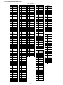
CD-C606/1900,CP-C606/1900
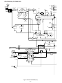
FM ANTENNA
IC301
TA7358AP
FM FRONT END
1 2 3 4 5 6
7 8 9
R301
10
C310
15P(CH)
C311 18P
C313
22P
(CH)
3
CF301
AM IF
R315
2
R323
220K
C314
0.0047
D
1
R312
47
C317
0.001
C315
0.0047
C316
0.022
R314
22
FM BAND
COVERAGE fL
VD302
SVC211C
R309
10K
T301
FM OSC.
T302 FM IF
R313
33K C312
0.022
C309
0.001
VD301
SVC211C
C304 C305
0.01 4.7P
L312
R311
100K
D301
DS1SS133
C308
FM RF 4.7P(UJ)
D304 DS1SS133
D303 DS1SS133
C319 0.001
C340 0.001
C303
10P
C
C307
10/16
R317 4.7K
R322
680
C318
100P
Q301
R391 KTC3194 Y
47
OSC BUFF
TP301
C356
0.022
C353 0.001
E
G
R343
68K
C336
560P
AM BAND
COVERAGE fL
FM SIGNAL
VD303
SVC348S
AM OSC
T333
C334
0.022
AM ANT
C331
0.022
F
R341
10K
C332
18P(UJ)
C330
10/16
T331
C352
12P(CH)
C333
0.047
AM TRACKING fL
C335
18P(UJ)
C351
0.001
H
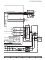
• NOTES ON SCHEMATIC DIAGRAM can be found on page 13.
3
4
Figure 18 SCHEMATIC DIAGRAM (1/10)
– 18 –
5
1 2
IC302
LC72131
PLL
CONTROLLER
MAIN PWB-A1(1/3)
2
22 21
C350
15P(CH)
AM SIGNAL
1
820
NC VSS
B
X IN X OUT
BF301
BAND PASS
FILTER
1 2 3
1
2
3
XL353
4.5MHz
FM 1
GND 2
AM 3
C306
0.022
AM LOOP
ANTENNA
C324
3.9P
(UJ)
CNP301
A
6
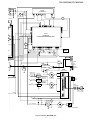
CD-C606/1900,CP-C606/1900
C382
0.0022
C387
3.3/25
C386
3.3/25
C395
1/50
NC VCO
C396
1/50
C394
0.015
C392
1/50
+B
R390
2.2K
R387
330
+B
L317
100µH
TUN_R
TUN_L
+B
2
1
3
Q351
KRA102 M
SWITCHING
BO1 FM IN
NC AM IN
SRSON/OFF
NC NC
SRS1/2
BO4 IO2
IO1 IF IN
1 2 3 4 5 6 7 8 9 10 11
R354 1K
R355 1K
R356 1K
R357 1K
R358 1K
R385
10K
ZD351
DZ5.1BSB
R353
2.2K
PD
DO VDD
DI A IN
CL
CE A OUT
X IN X OUT
Q381
KRA109 M
3
R388
3.3K
+12V
(AUDIO)
GND
(A_GND)
GND
(D_GND)
2
3
4
5
R361
47K
302
2131
LL
ROLLER
DO
CL
DI
CE
7
1
8
9
10
Figure 19 SCHEMATIC DIAGRAM (2/10)
– 19 –
11
6
7
8
9
12
TO MAIN SECTION
P21 12-C
C357
47/16
22 21 20 19 18 17 16 15 14 13 12
NC VSS
AM
/FM
C383
220P
C393
0.015
1
3 CF351
AM IF
+B
R351
1.5K
12
2
+B
C356
0.022
0.001
11
R386
390
AM IF
1
9 10
R384
15K
VR381
6.8K(B)
VCO
R383
1.2K
13
C341
0.001
2
C388 0.0015
15 14
AM
IF
GND
ST
IND
DET
OUT
TUN
IND
L CH
MPX
–IN
R CH
FM–
M/ST
5 6 7 8
+B
TP303
R398
5.6K
16
17
D381
DS1SS133
C354 R352
1/50 10K
C384
0.018
R380 3.9K
4
T382
C355
100P
TP301
18
R389
10K
C390
0.022
820
R382
1.5K
C385
3.3/25
C391
22/16
2 3
20 19
C389
0.022
1
TP302
R381
33K
FM
DET
T381
FM DET
FM IF AM
IN OSC
AM
+B
AM
RF
FM
AM +B
MIX
24 23 22 21
C381
220/10
C380
0.022
IC303
LA1805
FM IF DET./FM MPX./AM IF
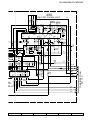
CD-C606/1900,CP-C606/1900
+B
IC401
M62439SP
AUDIO PROCESSOR
C411 0.033
R401
330
R412
330
R410
3.3K
Q401
KTC3199 GR
C401 R405
0.001 2.2K
C404
10/50
C451
0.001
R408
4.7K
11
12
13
14
15
R402
330
CD_+B
R409
4.7K
C452
0.001
R411
3.3K
C403
22/25
L_IN
A_+12V
+B
Q508
KRC104 M
0V
R502
10K
G
0V
R506
3.3K
0.7V
0V
0V
0V
R507
2.2K
2
0V
R518
1K
21
–
112K
+
Hich=T1
+
112K
–
C517
0.033
R523
27
NC
20
Q505
2SC2389 SE
SWITCHING
3
4
Figure 20 SCHEMATIC DIAGRAM (3/10)
– 20 –
5
68K
R537
5.6K
C526
0.001
R541 560
6
C521
1/50
C523
0.022
R532
1K
7
C519
180P
R534
33K
R538
5.6K
• NOTES ON SCHEMATIC DIAGRAM can be found on page 13.
2
18
NC
5
H
1
R53
19
IC501
AN7345K
4
3
C512
330P
C515
220/10
R539
6.8K
R524
100K
R526
4.7K
22
C510
330P
0.7V
0V
1
23
C520
1/50
C527
0 001
C504
180P
0V
C509
330P 24
C511
330P
R542
560
R505
Q503 3.3K
2SC2389 SE
0V
0V
0V
R513
4.7K
Q502
2SC2389 SE
SWITCHING
R504
2.2K
0.7V
R517
1K
R531
1K
R540
6.8K
CNP502
0.7V
0V
C503
180P
R512
47K
C518
180P
C514
220/10
R515
1K
0V
R533
33K
R522
27
C516
0.033
C552
0.01
TAPE2_L2
0V
Q509
KRC104 M
SWITCHING
R510
4.7K
7
0V
3.4V
R514
1K
C502
0.001
1
2
3
4
5
6
7
Q
KTC3
3
2
9.3V
C508
100/16
1
0V
R511
47K
RECORD/
PLAYBACK HEAD
8.6V
1
C525
3.3/50
9.3V
1
2
3
R501
10K
L-CH
CNS102
1 M_GND
2 ERASE
3 TAPE2_R2
4 A_GND
5 TAPE2_R1
6 TAPE2_L1
3
R509
10K
C501
0.001
Q504
2SC2389 SE
CNS101
1 TAPE1_R
2 A_GND
3 TAPE1_L
3.4V
2
C551
0.01
R508
10K
R561
22K
M_GND
0V
16
CNP501
R-CH
R418
5.6K
R516
150
TAPE1
PLAYBACK HEAD
TAPE2
11
R417
560 (1/2W)
C405
10/50
+B
E
ERASE
HEAD
C416
0.22(ML)
R_IN
Q501
KTA1266 GR
SWITCHING
F
13
12
A_GND
R503
10K
L-CH
14
R407
22K
C505
0.047
R-CH
1.5
C45
C415 0.0
0.033 (ML)
17
NC 16
15
C412 0.22
(ML)
C410
0.22
10
(ML)
C413
R413
10/50
C414
2.2K
0.022
(ML)
ZD401
DZ2.4BSB
1.5K
1.5K
R420
CD_GND
Q507
KTC3199 GR C507
0.001
D
10
R406
2.2K
C402
0.001
Q402
KTC3199 GR
Q506
KTC3199 GR
C506
0.001
TO POWER SECTION
P22 1-E
C
R422
R421
C422
10/50
C453
0.0022(ML)
19
18
C417
10P(UJ)
1.5K
1.5K
1.5K
C418
4.7/50
20
R419
10K
R416
R415
R414
1
2
3
4
5 NC
6
7
8
9
R423
22K
C406
4.7/50
R525
100K
R527
4.7K
CNS401
R451
1.8K
R-CH
1
A_GND
2
L-CH
3
CD_GND
4
+7V
5
+12V
6
R452
1.8K
1
2
3
4
5
6
+B
BI401
B
TO CD SERVO PWB
P27 12-C
CNP11
A
6
CD-C606/1900,CP-C606/1900
PLAYBACK SIGNAL
RECORD SIGNAL
+B
FM SIGNAL
1.5K
1.5K
R420
1.5K
C454
0.0022
C415
0.033 (ML)
C424
0.22
(ML)
TUN_R
A_GND
TUN_L
R425
330
–B
0V
Q513
0V
KTC3199 GR
SWITCHING
C538
470P
12
C535
1/50
C533
0.0033
–VP
VF1
D_GND
M_+12V
+B
+B UN_SW_+5V
SW_+5V
+B
M_GND
R555
47K
11.7V
11.6V
+B
R556
4.7K
0V
0V 1
R552
150
(1/2W)
R553
100K
11.6V
3
10
0V
AC_RLY_CONT
Q515
KRC104 M
POWER
–15V
M_+12V
-B
0V
+B
0V
Q516
0V
KTC3203 Y
R557
C539
12
0.0039(P.P.)
C540
0.027(ML)
C53
0.068
NC
2
R554
47K
FW703
VF2
L503
330µH
11
IC501:PLAYBACK AND
RECORD/PLAYBACK AMP.
GND Vcc
10
R548
10K
R545
56
C527
0.001
R538
5.6K
S_MUTE 1
R551
220
Q514
KTA1266 GR
C537 220/10
R547
10K
C536 22/16
C534
1/50
13
C529
22/16
R542
560
C525
3.3/50
9
14
ALC
RIPPLE
8
15
NC
Nor/CrO2
56K
Hich=CHROME
+
56K
–
R540
6.8K
7
–
+
FW701
9
+B
16
17
1
T_T1T2
POWER
AC_RLY_CONT
C528
22/16
18
R550
82K
R544
56
C532
0.0033
C530
0.068
68K
R537
5.6K
C526
0.001
R541 560
R539
6.8K
R53
R549
10K 0.7V
0.7V R546
10K
CLK
DO
CE
DI
REC/PLAY
T_BIAS
TO DISPLAY PWB
P25 8-G
REC_R
Q512
KTC3199 GR
0V SWITCHING
+B
REC_L
R543
82K
IC501
AN7345K
2
6
9
8
7
5
3
–B
+B
0V
1
4
DO
CE
DI
CLK
D_GND
A_+12V
C422
10/50
C423
0.022
ZD402
DZ2.4BSB
R423
22K
R424
820(1/2W)
–B
C417
10P(UJ)
R430
15K
R426
2.2K
TO DISPLAY PWB
P24 6-G
C416
22(ML)
CD SIGNAL
+B
C541
47/16
17
18
19
20
VF1
–VP
VF2
UN_SW_+5V
22
D_GND
SW_+5V
25
21
23
24
26
TO POWER SECTION
P22 1-G
2
1
R428
15K
TO TUNER SECTION
P19 12-F
C418
4.7/50
MAIN PWB-A1(2/3)
7
8
9
10
Figure 21 SCHEMATIC DIAGRAM (4/10)
– 21 –
11
12
CD-C606/1900,CP-C606/1900
IC601
LA4282
POWER AMP.
0V
0V
0V
0V
0V
0V
0V
0V
0V
0V
0V
0V
FM SIGNAL
–IN_A
+IN_A
RIPPLE_FILTER
GND_PRE
+IN_B
–IN_B
OUT_B
MUTE
GND_POWER
+VCC
OUT_A
GND_POWER
A
R607
C607
1K C616
0.082(ML)
82P
R606
C608 1K
R608
C606
120 C610
0.082(ML) 100/25
470/25
R612
4.7
R633
56K
1 2 3 4 5 6 7 8 9 10 11 12
C601 R601
10/16 4.7K
C605
100/25
R603
3.3K
R604
3.3K
C602
10/16
IC901
CONSTANT VOLTAGE
REGULATOR
+B
14
15
16
10
18
+B
D902
DS1SS133
3
C635
10/50
IC903
KIA7812P 1
C908
0.1
(ML)
C907
100/16
C906
0.022(ML)
D901
DS1SS133
R901
10K
3
C904
0.047(ML)
13
L_IN
A_GND
R_IN
A_+12V
M_GND
IC901
AN78L05 1
R611
4.7
IC903
VOLTAGE REGULATOR
+B
+B
2
C902
0.022(ML)
12
C901
47/16
+B
TO MAIN SECTION
P20 1-D
2
C912
2200/50
C910
0.1
(ML)
CD+B
CD GND
VOLTAGE REGULATOR
IC902
+B
3 KIA7806P 1
C911
3300/25
E
C633
220P
R922
2.2
D
C611
0.047
(ML)
R610
270
(1/2W)
Q631
1
R632
0V
KRC102 M 1 0V
820
2
0V
3
2
3
0V
0V 0V
Q632
R631 KRC102 M
R921
22K
2.2
+B
C634
0.022
(ML)
C612
0.047
(ML)
C604
0.001
R602
4.7K
C
C609
470/25
R609
270(1/2W)
C603
0.001
C631
0.022
(ML)
R605
120
B
C632
47/25
C615
82P
2
C903
47/25
C905
0.047(ML)
D903
DS1SS133
D904
DS1SS133
C909
0.1 (ML)
F
TO MAIN SECTION
P21 12-G
D905
1N4004S
26
19
20
21
22
23
24
25
18
17
SW_+5V
–15V
M_+12V
VF1
–VP
VF2
UN_SW_+5V
D_GND
C913
1000/25
+B
-B
-B
D906
1N4004
C9
100
+B
22
+B
+B
D919
DS1SS1
Q902
KRC107 M
+B
POWER
AC_RLY_CONT
3
0V
G
0V
2
1 0V
+B
D918
DS1SS133
C925
1000/6.
MAIN PWB-A1(3/3)
H
• NOTES ON SCHEMATIC DIAGRAM can be found on page 13.
1
2
3
4
Figure 22 SCHEMATIC DIAGRAM (5/10)
– 22 –
5
6
CD-C606/1900,CP-C606/1900
HEADPHONES PWB-A3
JK601
HEADPHONES
FW601
1
1
5
5
R614
330
R613
330
L-CH
L-CH GND SO601
SPEAKER
R-CH GND TERMINALS
R-CH
D915
RL203F
C922
0.1(ML)
D916
1N4004S
C923
0.047(ML)
1
2
2
3
3
4
4
1
2
C924
0.047(ML)
D917
1N4004S
D913
1N4004S
1
5
5
6
6
1
2
NC
T.F.
R904
220(1/2W)
R902
220(1/2W)
+B
CNS902
CNP902
C919
100/50
C918
47/50
D907
1N4004S
AC POWER
SUPPLY CORD
AC120V 60Hz
C920
100/50
+B
IC904
AN78L05
CONSTANT
VOLTAGE REGULATOR
5V
D918
DS1SS133
C926
10/16
3
2
D920
DS1SS133
PT902
D921
1SS133
1
D922
1SS133
D923
1SS133
D924
1SS133
C928
0.047
(ML)
C925
1000/6.3
7
SO901
AC SOCKET
D909
1N4004S
Q901
KTA1266 GR
D919
DS1SS133
R908
220
D908
1N4004S
C917
47/50
ZD901
DZ6.2BSA
C914
100/25
C927
470/25
3
25
R905
100
D906
1N4004S
R906
3.3K
C916
47/50
C915
100/35
R903
12K
ZD902
DZ300BSB
D905
1N4004S
C929
0.0047
D912
1N4004S
C921
0.1(ML)
RL901
RELAY
D911
RL203F
D914
RL203F
D925
1SS133
D910
RL203F
CNP901
C912
2200/50
CNS901
PT901
POWER
TRANSFORMER
POWER TRANSFORMER
8
9
10
Figure 23 SCHEMATIC DIAGRAM (6/10)
– 23 –
11
12
CD-C606/1900,CP-C606/1900
NC
NC
C774
100/10
Q703
KRC107 M
2
3
R791
1K
1
R792
33
B
C706
0.022
3 4 5 6 7 8 9 10 11 12 13 14 15 16 17 18 19 20 21 22 23 24 25 26 27 28 29 30 31 32 33
C707
220/6.3
1 2
NC
NC
P15
P16
P13
P20
P14
P11
P10
P9
P8
P7
P6
5G
P5
P4
6G
7G
P3
P2
8G
P1
P12
P19
P18
P17
1G
2G
3G
4G
9G
F
F
A
F
F
FL701
FL DISPLAY
1K
1K
1K
1K
1K
1K
1K
1K
1K
1K
1K
1K
1K
1K
R722
R724
R726
R728
7G
8G
1G
2G
3G
4G
9G
C775
2.2/50
26 A/D KEYIN 2
27 A/D KEYIN
IC701
IX0282AW 28 A/D DIST
SYSTEM MICROCOMPUTER
72 S5
71
70 S6
69 S7
CD FRF
A/D T2 RUN
OPEN 31
32
VSS 33
34
66 S10
36
1
SWM3
FOOL PROOF
CNPM2
SWM4
F.A.S
SOLM1
SOLENOID
2
SWM5
CAM
9
10
11
12
T1 RUNPALS
SOLENOID
MECHA STOP
2
R748
10K
R772
3.3(1/2W)
R747
10K
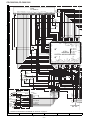
• NOTES ON SCHEMATIC DIAGRAM can be found on page 13.
1
R727 1K
R719 R721 1K
1K
R723 NC
1K
R716 1K
R712 2.2K
TO MAIN PWB
P21 12-F
1
FWM2
H
R746
10K
1
3
4
Figure 24 SCHEMATIC DIAGRAM (7/10)
– 24 –
5
6
SW +5V
R743
1.2K
1
2
3
4
5
6
7
FOOL PROOF
8
9
T1 RUNPALS 10
SOLENOID
11
MECHA STOP 12
BI702
S_MUTE
SPN_P
MOTOR
2 PHM1
PHOTE
INTERRUPTER
3
+B
T2 RUNPALS
C772
0.022
MOTOR
4
CNS702
MOTOR
1
2
3
GND
4
+B
5
T2 RUNPALS
6
7
FOOL PROOF
8
A/D T2 RUN
+B
M_GND
1
R725
1K
+B
8 7 6 5 4 3 2 1
CAM SW
SOLENOIDO
T1FAS
FPA
M
MM1
TAPE MOTOR
CNPM1
FWM1 2 +
40
C
C
C
+B
C773
0.0047
R800
10
(1/2W) R740
10K
TAPE MECHANISM
PWB-E
R745
10K
R742
10K
C705
47/16
+B
G
R707 1K
R709 1K
R702 1K
R714
2.2K
Q701
KTA1273 Y
Q702
D701
KTA1271 Y DS1SS133
F
R703 1K
R775 1K
+B
39
VF2
-VP
VF1
D_GND
M_+12V
UN_SW_+5V
+B
P15
R701 1K
P16
E
37
38
R749
10K
65 S11
P20 64 63 62 61 60 59 58 57 56 55 54 53 52 51 50 49 48 47 46 45 44 43 42 41
P13
R739
10K
26
35
68 S8
67 S9
65
3
R
R
R
27
R
28
A
29
A
30
25
R729
1K
D
25 A/D KEYIN 1
80 T7
75 S2
74 S3
73 S4
T.MOTOR
T.SOL
CAM SW
IC
REMOCON
SYSTEM STOP
C704
1/50
77 S0
76 S1
T1FAS
VDD
P17
P18
P19
P12
P1
P6
VLOAD
P7
P8
P9
P10
P11
P14
S12
S13
S14
S15
SPN_P
DIST0
POWER
AC RLY CONT
S MUTE
OPEN
FPA
C703
1/50
79 T8
78 LCK
TAMUTE
T T1T2
T_BIAS
REC/PLAY
CD U/D SW
6G
80
5G
RESET
CD SQOUT
TIMER LED
AVSS
CD CQCK
CD DSP RES
1 2 3 4 5 6 7 8 9 10 11 12 13 14 15 16 17 18 19 20 21 22 23 24
T6
T5
T4
T3
T2
T1
T0
VDD
DO
DI
CE
CLK
CD RWC
CD WRQ
CD PCCL
CD COIN
C
R704
R705
R706
R708
R710
R711
R713
R715
R717
R718
C709
R741
100K
CD-C606/1900,CP-C606/1900
+B
R758
1.8K
SWITCH PWB-A4
R762
1.2K
EYIN 1
EYIN 2
EYIN 3
CD FRF
A/D T2 RUN
R735
R736
26
R737
27
R738
28
AVDD
29
AVREF
30
25
1K
1K
1K
1K
LED701
SLI342UCJ1
TIMER
10K
10K
10K
R763
820
ER
R764
820
TAMUTE
T T1T2
T_BIAS
REC/PLAY
CD U/D SW
36
37
38
39
40
R767
1.5K
R770
1.8K
R766
1.2K
R768
1.5K
SLM +
SLM –
PUIN SW
O/C SW
DISC NO SW
SW708
OPEN/
CLOSE
SW707
DISC
SKIP
R773
2.2K
R776
3.3K
R730
R731
R732
R733
R734
STOP
TUNER
/BAND
TAPE
R771
1.8K
R774
2.2K
R777
3.3K
CD
SW719 SW720 SW721 SW722
TUNING TUNING
FAST
DOWN
UP
FORWARD
C701
15P (CH)
CD
CD
CD
CD
CD
R765
1.2K
SW716 SW717 SW718
+B
34
35
R780
3.9K
1
3
3
RECORD MEMORY
REWIND /PAUSE
/SET
XL701
4.19MHz
32
VSS 33
FW705
SW709 SW710 SW711 SW712 SW713 SW714 SW715
OPEN 31
IST
1
POWER CLOCK TIMER/
SLEEP
R754
R756
R757
R753
10K
R722
R724
R726
R728
AVSS
CD CQCK
CD DSP RES
20 21 22 23 24
R778
8.2K
SW701 SW702 SW703
1K
1K
1K
1K
R755
3.3K
R752
10K
C709
0.022
R761
820
PLAY
VOLUME VOLUME X-BASS
/DEMO
DOWN
UP
C702
18P(CH)
1K
1K
1K
1K
1K
+B
R785
4.7K
R750
10K
C772
0.022
1
D704
DS1SS133
RX701
REMOTE
1 2 3 SENSOR
C714
0.022
IC702
2
C713
0.022
1
3
IC702
KIA7042P
RESET
RESET
Q704
KRC102 M C712
3.3/50
2
3
R783
100K
C710
0.01
R751
10K
R782
47K
+B
D705
DS1SS133
D743
DS1SS133
D703
DS1SS133
C708
0.001
R749
10K
R748
10K
L701
100µH
D702
DS1SS133
+B
+B
R725
1K
R772
3.3(1/2W)
1K
+B
C770
0.1/50
R729
1K
R727 1K
R723 NC
1K
45 44 43 42 41
R786
100
C715
47/25
+B
+B
CE
DO
CLK
FW701
FW703
TO MAIN PWB
P21 12-E
AIN PWB
1 12-F
DISPLAY PWB-A2
15 14 13 12 11 10 9 8
7 6 5 4 3 2 1
15 14 13 12 11 10 9 8
7 6 5 4 3 2 1 CNS701
BI701
D_GND
FRF
DSP RES
CQCK
SQOUT
COIN
WRQ
RWC
REC/PLAY
DI
1
9
PCCL
U/D SW
DISC NO SW
O/C SW
PUIN SW
SLM–
SLM+
10
AC_RLY_CONT
POWER
T_T1T2
T_BIAS
SW_+5V
M_GND D707
DS1SS133
VF2
-VP
VF1
D_GND
M_+12V
UN_SW_+5V
D708
DS1SS133
CNP12 TO CD SERVO PWB
P27 7-H
7
8
9
10
Figure 25 SCHEMATIC DIAGRAM (8/10)
– 25 –
11
12
CD-C606/1900,CP-C606/1900
C34
0.33/50
Q1
2SA1318
LASER DRIVER
–
+
CE
DAT
CL
CLK
FSS
DRF
VCC2
VR
REF1
LF2
R45
4.7K
R39
1K
C27
0.001
42
41
HF
TP1
R38
470
39
38
37
36
TOFF
35
TGL
JP+
SL+
JP–
R43
56K C23
0.0027
34
33
R33 R32
1.2K 10K
C21
0.0033
C22
220P
R36
220K
C20
47/16
R42
47K
R35
220K
C18
0.47/50
R41
47K
R40 C25
5.6K 27P
SLD
29 30 31 32
R34
1K
C12
0.1
R44
33K
40
SLOF
SL–
REF
SLEO
SPO
SP–
10K
56K
R28
R29
C16
0.0047
C13
330P
SPG
REF
R31
1.2K
R30
6.8K
C26
0.033
43
HFL
TES
C19
1/50
FE1
REF
AGND
SP
FE–
FA–
SPI
REF
SLOF
SLOF
S.Q.R
THD GL
REF
–
+
FA
R23
10K
R21 R20
1.5K 1K
R22
820
1M
–
+
2200P
1M
2200P
–
+
–
+
R27
39K
R25
1.5K
C17 27 28
0.001
24 25 26
RFSM
CV–
OR
SLOF
REF
45
44
C24
2.2P
CV+
–
+
–
+
R24
47K
R26
82K
C14
0.01
RF
–
+
REF
CV+
JP–
JP+
JPCLO
REF
FE
18 19 20 21 22 23
VREF
TR+
FO+
C57
0.001
GND
C35
1/50
R37
82K
D1
1SS133
CNP2
C76
0.022
TR–
TR+
FO+
FO–
11 GND
13
14
15 SL–
16 SL+
C36
100/16
SPIN
6
5
4
3
2
1
SOL– 37
SOL+ 36
35
34
33
+B
31
+B
30
29
VCC3 28
C77
100/16
SP+ 27
SP– 26
18 VCC1
SPO 25
19 STANDBY
+B
C82
100/16
GND 32
17 SLD
R56
6.8K
6
5
4
3
2
1
CNP3
CNP3A
6
5
4
3
2
1
M– 39
M+ 38
(SPN)VCC2 24
20 Vref
SOLD 23
21 MUTE
SOL– 22
R47
10K
+B
SP+
SP–
SL_+
SL_–
CD_PUIN
RWC(DSP)
WRQ(DSP)
CO IN(DSP)
SQ OUT(DSP)
CQ CK(DSP)
RES(DSP)
DRF (ASP)
D_GND
M
6
5
4
SLIDE 3
–
2
PU-IN
1
–
+
CNS3A
M2
SLID
MOTOR
SW4
PICKUP IN
+
CNS3B
M
TR–
10
C55
100/16
CD MOTOR
PWB-C
TR+
12
CD_GND
F
1
2
3
4
5
6
7
LD
8
VCC4 40
FO (GAIN)
FO+
C37
0.022
PD
CNS2A
TR–
1
TR+
2
FO+
3
FO–
4
GND
5
PD
6
VR
7
LD
8
TR–
TR+
FO+
FO–
GND
PD
VR
LD
FD
FO–
+B
LD_M+ 42
LD_M– 41
TO
CNP12
SLD+
1
2
3
4
5
6
7
8
9
IC3
M63001FP
FOCUS/TRACKING/SPIN
/SLIDE DRIVER
FO–
TR–
CNS2B
1
2
3
4
5
6
7
8
G
FSTA REF
JP
REF
CV–
–
+
R19
1K
ACTUATOR
M1
SPINDLE
MOTOR
–
+
E
RFS–
–
+
1
2
3
4
5
6
7
8
JP FSC
REF FOSTA
TO
GEN
GEN
REF
R18
15K
C11
0.1
TGL1
THDL
REF
FD–
17
R17
33K
SLC
–
+
5
4
3
2
1
TD
–
+
1/16
GEN
TD–
14 JP
TO
15
16 FD
REF
VCC
–
+
13
SLI
CL
FSTA
8/12CM
–
+
PICKUP UNIT
VCR
–
+
R14 R15 C10
27K 12K 180P
R16
3.3K
REF
CE
2FREQ
LASER
DRF
IC1
LA9241M
SERVO AMP.SLOF
REF
11
C28
0.1
46
DGND
TOSTA
REF
C7
0.1/50 TH
10
C8
NC
0.068
12
–
+
FSC
FOSTA
–
+
C
HFL
LATOH
6 TE–
7 TE
C5
C54 R10 0.033
0.001 2.2K
8 TESI
C6
0.033
R11
9 SCI
6.8K
R12
100
R13 C9
1K 0.047
PHI
REF –+
VCR
DEF
–
+
VCR
TB
5
R8
15K
NC 48
TBC 47
EFBAL
–
+
R9
100K
VCR
REF
–
+
C4
0.1/50
REF –+
REF
D
BHI
LDO
3
4 F
55 54 53 52 51 50 49
DEF
56
57
58
–
+
K
1
A
2
B
3
E
4
F
5
CNP1
TE
K
E
A
B
F
59
64 63 62 61 60
VCC1 LDS
–
+
RF
1 FIN2
REF –
+
2 FIN1
FE1
–
REF –
+
+
REF
E
–
+
CNS1A
1
2
3
4
5
–
+
B
CNS1B
K 5
E 4
A 3
B 2
F 1
C29
4.7/50
C3
1/50
C30
0.1/50
R1
22
R46
560
C2
0.01
C31
220/6.3
C1
47/16
C32
0.01
C15
0.01
A
C33
0.47/50
R2
1K
1 2 3 4 5 6 7 8 9
CNS7
P25 10
FROM DISPL
H
• The numbers 1 to 12 are waveform numbers shown in page 14.
• NOTES ON SCHEMATIC DIAGRAM can be found on page 13.
1
2
3
4
Figure 26 SCHEMATIC DIAGRAM (9/10)
– 26 –
5
6
CD-C606/1900,CP-C606/1900
CD SERVO PWB-B
R57 1K
R58 1K
R59 1K
PW
NC
C49
100P(CH)
XL1
16.93MHz
R88
R89
R90
R91
CD_LCH
VOLTAGE
REGULATOR +B
C50 C51
0.022 100/16
R64
22
R66
220
C75
0.001
+B
+B
+B
C56
0.022
C57
0.001
+B
+B
+B
+B
R80
820
R83
390
D92
1SS133
D93
1SS133
R82
390
2
Q51
KRC102 M 1
SWITCHING
DRIVER
R81
820
3
R84
2.2K
SOLM2
SOLENOID
D91
1SS133
CNS10
CNP10
SOL+
1
SOL–
2
M+
3
M+
M–
4
M–
5
GND(D)
OPEN CLOSE 6
CD_D_NO
DISC NO. 7
8
GND(D)
MECHA UP 9
10 GND(D)
10
BIM5
1
2
3
4
5
6
1
2
3
4
5
6
7
8
9
SW2
MECHA
UP
+
–
M
M3
TURNTABLE
UP/DOWN/
LOADING
MOTOR
SW1
OPEN CLOSE
TRAYMOTOR
PWB-D
CNS5
1 1
2 2
SW3
DISC
NUMBER
SLD+
SLD–
PUIN SW
OP/CLOS
DISC NO.
UP/DOWN
PCCL
C37
0.022
R47
10K
SQ OUT(DSP)
CQ CK(DSP)
RES(DSP)
DRF (ASP)
D_GND
1
2
3
4
5
6
4 5 6 7 8 9 10 11 12 13 14 15
CNS701
P25 10-H
ROM DISPLAY PWB
7
8
9
10
Figure 27 SCHEMATIC DIAGRAM (10/10)
– 27 –
11
12
CNS401
P20 1-A
FROM MAIN PWB
D82
1SS133
L61
0.82µH
32
PIN27
TRY SPEED
HIGH
LOW
R55
100
L-CH
D-GND
+7V
+12V
A_GND
ZD61
MTZJ5.6B
C43
330/6.3
R-CH
A_GND
CD_RCH
C52
100/16
C71
10/50
R73 R74
100K 100K
R71
2.7K
TEST3
NC
DOUT
NC
D81
1SS133
R72
2.7K
R65
1K
24 25 26 27 28 29 30 31
1.2K
1.2K
220
1K
LVSS 38
LCHO
37
LVDD 36
MUTEL(NC)
35
DIGITAL PCCL 34
OUT
TEST4 33
EMPH
NC
C2F
NC
CONT4
CONT3
CONT5
FSEQ
NC
VDD
NC
17 18 19 20 21 22 23
CONT2
EXTERNAL
OUTPUT
RVSS 39
CNP11
C72
10/50
+5V
Q52
KTC3203 Y
1BIT
DAC
SERVO/SIGNAL
CONTROL
PCK
JP_
JP+
TGL
4FS
DIGITAL
FILTER
SYNC-DETECT
EFM DEMODULATE
44
XVDD 43
MUTER
42
NC
RVDD 41
RCHO 40
C83
0.022
XOUT
R93
220
45
C73 C74
220P 220P
FSX
NC
SBCK
SFSY
NC
WRQ
SQOUT
ERROR
COERECT
FLAG
CONTROL
SERVO
TES COMMAND
TOFF
RWC
COIN
/CQCK
VCO
CLOCK
OSC
CONTROL
HLF
C22
20P
X-TAL
GENERATOR
2KX8
IC2 RAM
LC78622N
SLICE
EFMIN LEVEL
10
CONTROL
11 TEST2
CLV+
CLV
12
CLV- DIGITAL
13
SERVO
V/P
14
16
48
SBSY
47
NC
XIN
R50 3 PDO
C39 680
0.047
4 VVSS
5 ISET
C40
0.047
R52
27K
6 VVDD
R53
7 FR
1.2K
8 VSS
EFMO
9
15
NC EFLG
SUB-CODE
XVSS 46
CONT1
R51
3.3M
16M
NC
TEST11 NC
/RES
/CS
TEST5
4M
TEST1
1 DEF1
2 TA1
+B
49
64 63 62 61 60 59 58 57 56 55 54 53 52 51 50
µ-COM
INTERFACE
C48
100P
R60 C46
1K 100P
(CH)
C38
0.01
C45
100P(CH)
R63
1K
C44
100P(CH)
R61 1K
R62 1K
C47
100P(CH)
CD SIGNAL
CD-C606/1900,CP-C606/1900
R613
5
R614
JK601
HEADPHONES
1
MAIN PWB-A1
D923
D924
R631
D632
5
1
C608
1
FW601
1
2
3
C602
WH
WH
WH
WH
WH
RD
R921
10
R904
C912
C905
C910
C904
C901
C911
CNP901
1 3 2
C909
2
FROM POWER
TRANSFORMER
CNS901
P31 8-G
C903
C908
C607
1
2
3
Q632
D903
D904
FW703
R612
IC902
3 2 1
R902
D631
C604
IC903
3 2 1
R901
C612
C929
C631
C603
R601
R604
R610
R605
C907
C610
C609
C
R603
C633
C632
C635
C611
R607
R632 C605
R633
R606
R611
RL901
SO901
AC SOCKET
AC120 60Hz
12 1110 9 8 7 6 5 4 3 2 1
Q631
3 2 1
Q902
SO901
IC601
R609
C926
D925
C906
D918
C615
C925
C616
D920
C634
D919
R908
D922
R602
3
B
C927
1C904
C928 1
D921 2
R608
PT902
POWER TRANSFORMER
C606
A
FW601
HEADPHONES PWB-A3
1
T333
C385
2
4
5
B
C
E
C916
C505
B C E
Q501
C541
6
R547
Q516
R509
R5
R5
R553
R537
R541
E
C
B
C534
C526
R539
Q512
C528
R544
R536
R543
C551
C538
C532
R533
R546
C520
C518
FW701
R502
C536
C535
C529
R545
C533 R548
R550
C523
C527
R540
R538
C525
C521
C519
C512
R523 C510
Q513
R542
C403
R417
C517 C552
C405
R527
R411
R532 R534
R531
15 13
C341
Figure 28 WIRING SIDE OF P.W.BOARD (1/4)
– 28 –
C531
R503
Q381
VR381
VCO
R
C
IC501
C509
R522
R524
R526
C516
Q504
R514 R515
C511
5
20
Q508 1 2 3
R384
3
B
C
E
10 12
1
24
TP302
1
C920
Q509 1 2 3
3
2
1 C388
C387
C383
D905
C914
R525
C423
R423 C417
ZD401
R419
R418
R386
C
R508
R398
C392
R385
C396
C386
T381
C501 C515
TP301 R389
C514
ZD351
L317 R388
R387
R383
C382
15 13
1 2 3 4 5 6 7
Q503
CNP502
B CE
E
E
E
C
C
R501 C
B
C503
B
B
R505
R390
C394
C357
R353
R352
R351
C354
D381
C393
IC303
20
12
Q505
C353
ZD402
CNP501
3 2 1
R511 C502
Q506
R510
B C E
R518
R513
R512
C506
B C E
R517
C504 Q507 C507
Q502
R504
R507
R506
R356
R354
R355
Q351
Q301
C350
C352
15
10 12
5
C389
C331
C356 IC302
C391
1
24
1011
5
1
R391 C318
T301
T382 CF351
1
2
3
R361
22 20
C381
1
2
3
T331
R358
C395
CF301
H
C307
C340
C310
R315
T302
R382
FM/AM LOOP
ANTENNA
D301
R381 C384
BF301
AM
D303
C309
C334 C317
R311
VD301
C316
R343
C332
C333 R317
R341 R313
C335
R309
C336 VD303
R312
C330
C355 C313
C390
C380
VD302
R380
C311 C324
D304
C319
1
2
3
CNP301
1
2
3
R314
C304
3
C315
2
L312
1 C314
C308
R357
1
2
3
R323
XL353
B
C
E
C312
R301
R322
C303 C305
IC301
1 2 3 4 5 6 7 8 9
F
C306
CNS902
C351
C915
C414
C410
R412
C424
R426
P31 11-G
C413
R425
R420
C418 R421
C415
C416
R428
C422
R413
C412
C411
1
2
3
4
5
6
CNP902
C924
D917
D912
D913
C923
D916
D915
FROM POWER
TRANSFORMER
R405
C406
R401
R410 E C B Q401
BI401 R416
R409
C404 R402
WH 6
R415
C402
C451
WH
R414
R406
IC401
R407
WH
R451
WH
R452
B C E
10
1
5
WH
C453 C454
RD
Q402
11
15
1
R422 20
R430
D911
E
C919
C401
D906
D909
D908
C601
C922
L-CH
FM
R408
C452
D910
R424
R-CH
SO601
SPEAKER
TERMINALS
GND
D907
ZD902
R905
R906
R903
D914
C921
R561
GND
G
ZD901
R922
D
R557
CD-C606/1900,CP-C606/1900
SWITCH PWB-A4
1
FW705
SW708
OPEN/CLOSE
SW707
DISC SKIP
R780
TO CD SERVO PWB
CNP12
P30 5-G
3
BL
BL
BL
BL
BL
BL
BL
BL
BL
BL
BL
BL
BL
BL
RD
15 14 13 12 11 10 9 8 7 6 5 4 3 2 1 CNS701
1
3
FW705
SW722
X-BASS/
DEMO
R777
R774
BLACK
PK
PINK
Q901
C918
SW713
C703
3
2
1
CD
CNS102
P31 10-E
SW714
TAPE
D705
D704
D702
SW715
R782
TUNER/BAND
FROM TAPE
MECHANISM
C540
3
2
1
D703
R783
C713
R785
D743
IC702
C712
Q704
1
LED701
C710
R554
C539
C775
SW710
C770
R553
R557
SW711
R776
L503
R761
R778
SW701
R762
C505
R552
B
C
E
R556
R555
Q514
B C E
Q516
R509
3
2
1
64 65
2
1
MEMORY/SET
REC/PAUSE
RD
1
80
REWIND
Q515
R547
C534
R537
R541
4
WH
GY
WH
R773
C530
C538
32
R706
R705
R704
R747
C773
GY
SW709
L701
R551
3
9
8
7
6
5
4
3
2
1
BI702
8
D701
R800
R516
C535
C536
C537
C529
R545
C533 R548
TO TAPE
MECHANISM
PWB
CNPM1
P31 12-A
CNS702
12 WH
11 GY
10 WH
R743
R502
P31 9-E
R549
C508
2
R708
R742
R745
B
C
E
33
32
31
30
29
28
27
26
25
24
23
22
21
20
19
18
17
16
15
14
13
12
11
10
9
8
7
6
5
4
3
R767
R765
R763
9
R712
B
C
E
R739
C705
R770
CNS101
R740
Q701
FROM TAPE
MECHANISM
Q702
FW701
FW701
STOP
9
R707
R775
R703
R702
R701
1
R709
1
C531
C714
R726
R728
SW716
R735
R736
R749
C707
R754
D708
R737
R753
R738 FAST
FORWARD
R730 C701 XL701
R750
C708
25 24
R731
R732 C702
SW719
30 20
R733
R751
R734
15
35
40
10
R729
R727 41
45
5
PLAY
IC701
R725
50
SW712
75
55
R723
60 70
R721 R719
R757
R756
R746
C913
C920
C709
R755
R716
R714
915
D905
TUNING UP
R748
C917
D907
ZD902
R905
R906
1
E
C
B
R771
10
C704
BK
1
2
3
SW702
SW703
CLOCK
TUMER
/SLEEP
C541
POWER
7
FL701
GRAY
WHITE
R792
R741
GY
WH(W)
SW717
SW718
TUNING
DOWN
Q703
VIOLET
R791
VL
C774
C706
BLUE
R713
R710
GREEN
BL
R758
R711
GR
3
2
1
R786
R724 R718
R717
R722
R715
YELLOW
R752
YL
R766
ORANGE
VOLUME
UP
R764
RED
OR
R768
CNS401
6
5
TO CD SERVO PWB
4
CNP11
3
P30 4-G
2
1
WH
WH
WH
WH
WH
RD
BROWN
RD(R)
D707
BR
VOLUME DOWN
FW703
COLOR TABLE
RX701
SW721
R772
D901
1 3 2 IC901
C902
C904
D902
C901
C772
03
04
BI701
C715
SW720
1
15
DISPLAY PWB-A2
8
9
10
Figure 29 WIRING SIDE OF P.W.BOARD (2/4)
– 29 –
11
12
CD-C606/1900,CP-C606/1900
A
CD MOTOR PWB-C
TRAY MOTOR
PWB-D
B
RD
WH
GY
WH
GY
WH
1
2
3
4
5
6
SW3
DISC NUMBER
+
CNS3A
M2
SLED MOTOR
-
1
2
3
4
5
6
1
2
3
4
5
6
M1
SPINDLE MOTOR
SW4
PICKUP IN
CNP3A
SOLM2
SOLENOID
+
CNS3B
-
M3
TURNTABLE UP/
DOWN LOADING
MOTOR
2 1
PICKUP UNIT
+
SW1
OPEN/CLOSE
BIM5
6
C
1
CNS1A
1
2
3
4
5
CNS5
2 1
BL
PK
WH
YL
BK
GY
5
1
1
8
1
2
3
4
5
6
7
8
CNS2A
CNS10
1
2
3
4
5
RD
WH
GY
WH
GY
WH
GY
WH
1
2
3
4
5
6
7
8
OR
BR
WH
GY
WH
GY
WH
GY
WH
RD
SW2
MECHA UP
D
CNS1B
BK
WH
PK
YL
BL
1
CNS2B
10 9 8 7 6 5 4 3 2 1
2
7 10 8
9
4
3
6
5
CD SERVO PWB-B
GRAY
WHITE
BK
BLACK
PK
PINK
R25
R51
R50
C56
R93
R55
R91
C43
R74
D82
C72
C73
R71
R65
C50
L61
C83
D81
CNP12
CNP11
6 5 4 3
15 14 13 12 11 10 9 8 7 6
2 1
CNS401
FROM MAIN PWB
P29 8-D
11
5 4 3 2 1
CNS701
FROM DISPLAY PWB
P29 11-A
H
• The numbers 1 to 12 are waveform numbers shown in page 14.
1
2
3
4
Figure 30 WIRING SIDE OF P.W.BOARD (3/4)
– 30 –
5
C37
C25
R40
R44
R88
R89
E
R47
C39
C40
C26
C27
R41
R42
C28
C29
XL1
R35
C71
R64
C
C51
B
R66
32 33
R90
R73
R81
R83
R80
C21
R34
R29
C19
R36
R72
C14
R26
C13
IC3
48
45
40
C74
GY
W H(W )
1
50
IC2
20
49
30 35
R32
R33
Q52
2
R62
55
15
C20
3
C49
R57
60
25
ZD61
VIOLET
R61
5
17
Q51
C52
BLUE
VL
C45
1 64
10
16
32 33
C17
R30
R31
R63
R58
40
C18
1
2
3
4
5
6
7
8
9
10
49
48
30 35
C75
BL
50
45
R19
D93
GREEN
R52
C22
C11
R56
R24
C16
R27
R28
R84
YELLOW
25
10
D92 R82
YL
GR
55
12
20
R23
C77
ORANGE
15
60
IC1
R45
R20
R22
R21
G
OR
16
17
R18
RED
C46
R60
R59
R38
R15
C10
5
10
1
C47
C38
R53
R17
5
40
42
BROWN
C57
1 64
R16
35
CNP10
RD( R)
20
C23
R39
C34
C12
C33
C55
C36
BR
D91
F
C32
R10
15
C82
COLOR TABLE
B
C9
25
30
E
C1
CNP1
R14
21
22
C
C2
C15
C24
C5
C30
C6
C76
R13
8
7
6
5
4
3
2
1
CNP2
E
1
2
3
4
6
5
R37
CNP3
R11
C31
R43
C7
Q1
R1
R8
R9
C35
C3
R2
R46
R12
1
2
3
4
5
C48
D1
C54
C4
C8
6
C44
CD-C606/1900,CP-C606/1900
TAPE MECHANISM PWB-E
FROM
DISPLAY
PWB
CNS702
SWM3
FOOL PROOF
12 11 10 9 8 7 6 5 4 3 2 1
FWM2
2
P29 8-F
CNPM1
FWM1
2
1
R
CNPM2
1
PHM1
4
3
SOLENOID
SOLM1
SWM4
F. A. S
MM1
TAPE MOTOR
+
BK
BK
WH
WH
SWM5
CAM
-
TAPE 1
TAPE 2
PLAYBACK HEAD
WH PK
ERASE HEAD
BK
RECORD/PLAYBACK HEAD
BL PK
BK
WH
BR
GY
YL WH BK
GY
COLOR TABLE
1 2 3
PK
BK
WH
YL
BL
WH
BK
WH
BR
PK
BK
1
2
1 2 3 4 5 6 7
CNS101
CNP501
P29 8 - F
TO MAIN PWB
CNS102
CNP502
P29 8 - G
TO MAIN PWB
BROWN
RD(R)
RED
OR
ORANGE
YL
YELLOW
GR
GREEN
BL
BLUE
VL
VIOLET
GY
GRAY
WH(W)
WHITE
BK
BLACK
PK
PINK
PT901
POWER TRANSFOMER
CNS902
YL
RD
YL
CNS901
TO MAIN PWB
CNP901
P28 1 - D
BR
2
1
BL
7
8
9
2
BR
4
5
WH
6
10
TO MAIN PWB
CNP902
P28 1 - F
3
WH
Figure 31 WIRING SIDE OF P.W.BOARD (4/4)
– 31 –
1
11
12
CD-C606/1900,CP-C606/1900
VOLTAGE
IC1
PIN VOLTAGE
NO.
1 2.5V
2 2.5V
3 2.5V
4 2.5V
5 2.5V
6 2.5V
7 2.5V
8 2.5V
9 2.5V
10 2.5V
11 2.5V
12 2.5V
13 2.5V
14 2.5V
15 2.5V
16 2.5V
17 2.5V
18 2.5V
19 2.5V
20 2.5V
21 2.5V
22 0V
23 2.5V
24 2.5V
25 2.5V
26 2.5V
27 2.5V
28 2.5V
29 2.5V
30 2.3V
31 2.3V
32 0V
33 0V
34 5.0V
35 5.0V
36 0V
37 0V
38 5.0V
39 0V
40 0V
41 1.6V
42 2.4V
43 2.4V
44 2.4V
45 0V
46 2.5V
47 2.5V
48 0V
49 0V
50 2.4V
51 4.6V
52 4.6V
53 0V
54 0V
55 5.0V
56 5.0V
57 2.5V
58 2.5V
59 1.0V
60 1.0V
61 2.2V
62 4.2V
63 0V
64 5.0V
IC2
PIN VOLTAGE
NO.
1 0V
2 0V
3 0V
4 0V
5 1.9V
6 5.0V
7 0V
8 0V
9 2.5V
10 2.4V
11 0V
12 0V
13 0V
14 5.0V
15 0V
16 0V
17 5.0V
18 5.0V
19 0V
20 0V
21 2.5V
22 0V
23 5.0V
24 0V
25 0V
26 0V
27 0V
28 0V
29 0V
30 5.0V
31 2.5V
32 0V
33 0V
34 0V
35 5.0V
36 4.6V
37 1.9V
38 0V
39 0V
40 1.9V
41 4.6V
42 5.0V
43 5.0V
44 2.1V
45 2.1V
46 0V
47 0.1V
48 2.3V
49 0V
50 2.5V
51 0V
52 2.5V
53 0V
54 0V
55 0V
56 4.6V
57 4.6V
58 4.7V
59 0V
60 2.3V
61 2.3V
62 0V
63 0V
64 0V
IC3
PIN VOLTAGE
NO.
1 2.5V
2 2.6V
3 2.9V
4 3.3V
5 3.3V
6 3.3V
7 3.3V
8 0V
9 0V
10 0V
11 0V
12 0V
13 0V
14 0V
15 3.3V
16 3.3V
17 3.0V
18 7.2V
19 5.0V
20 2.5V
21 0V
22 0V
23 0V
24 7.2V
25 2.5V
26 3.3V
27 3.3V
28 11.2V
29 0V
30 0V
31 0V
32 0V
33 0V
34 0V
35 0V
36 5.3V
37 5.3V
38 3.3V
39 3.3V
40 7.2V
41 0.1V
42 0.1V
– 32 –
IC301
PIN VOLTAGE
NO.
1 0.9V (0V)
2 1.6V (0V)
3 6.0V (0.4V)
4 1.6V (0V)
5 0V (0V)
6 6.0V (0.3V)
7 5.2V (0.2V)
8 5.9V (0.3V)
9 6.0V (0.3V)
IC302
PIN VOLTAGE
NO.
1 2.5V (2.5V)
2 0V (0V)
3 0V (0V)
4 0V (0V)
5 4.5V (4.5V)
6 4.5V (4.5V)
7 0.2V (11.9V)
8 0V (0V)
9 0V (0V)
10 0V (0V)
11 5.1V (5.1V)
12 0V (0V)
13 0V (0V)
14 0V (0V)
15 0V (2.5V)
16 2.5V (0V)
17 5.1V (5.1V)
18 0.9V (0.9V)
19 0.9V (0.9V)
20 1.3V (1.1V)
21 0V (0V)
22 2.5V (2.5V)
IC303
PIN VOLTAGE
NO.
1 1.6V (1.6V)
2 1.6V (1.6V)
3 7.1V (8.1V)
4 0.2V (0.6V)
5 1.6V (1.6V)
6 0V (0V)
7 5.1V (5.1V)
8 0V (0V)
9 2.3V (2.3V)
10 2.3V (2.3V)
11 6.4V (8.1V)
12 0.9V (0.9V)
13 1.1V (2.1V)
14 1.8V (1.6V)
15 2.2V (1.3V)
16 1.7V (1.7V)
17 1.6V (1.7V)
18 1.6V (1.6V)
19 0.4V (0.5V)
20 7.1V (8.1V)
21 7.1V (8.1V)
22 1.7V (1.7V)
23 1.7V (1.7V)
24 1.7V (1.7V)
IC401
PIN VOLTAGE
NO.
1 0V
2 0V
3 0V
4 0V
5 0V
6 0V
7 0V
8 0V
9 0V
10 2.7V
11 0.2V
12 –2.7V
13 0V
14 0V
15 0V
16 0V
17 0V
18 0V
19 0V
20 0V
IC501
PIN VOLTAGE
NO.
1 0V (0V)
2 0V (0V)
3 0.5V (0.5V)
4 4.3V (4.3V)
5 0.2V (0.3V)
6 1.3V (1.3V)
7 0V (0V)
8 0.6V (0.6V)
9 4.1V (4.1V)
10 4.0V (4.0V)
11 0V (0V)
12 0V (0V)
13 8.1V (8.1V)
14 4.8V (4.8V)
15 0V (0V)
16 4.1V (4.1V)
17 0.6V (0.6V)
18 0V (0V)
19 2.5V (2.6V)
20 0.2V (0.3V)
21 4.3V (4.3V)
22 0.5V (0.5V)
23 0V (0V)
24 0V (0V)
CD-C606/1900,CP-C606/1900
TROUBLESHOOTING
When the CD does not function
When the CD section does not operate. When the objective lens of the optical pickup is dirty, this section may not operate. Clean
the objective lens, and check the playback operation. When this section does not operate even after the above step is taken, check
the following items.
Remove the cabinet and follow the troubleshooting instructions.
"Track skipping and/or no TOC (Table Of Contents) may be caused by build up of dust other foreign matter on the laser pickup
lens. Before attempting any adjustment make certain that the lens is clean. If not, clean it as mentioned below."
Turn the power off.
Gently clean the lens with a lens cleaning tissue and a small amount of isopropyl alcohol.
Do not touch the lens with the bare hand.
Dust gradually accumulates on the objective lens during use, and it may degrade performance. To avoid this problem, use a
cleaning disc designed for CD optical pickup lenses.
HOW TO USE
1. Using the brush in the cleaner cap, apply 1 or 2 drops of the cleaning fluid to the brush on the CD cleaner disc which has
the mark next to it.
2. Place the CD cleaner disc onto the CD disc tray with the brush side down, then press the play button.
3. You will hear music for about 20 seconds and the CD player will automatically stop. If it continues to turn, press the stop
button.
CAUTION
The CD lens cleaner should be effective for 30~50 operations, however if the brushes become worn out earller then please
replace the cleaner disc.
If the CD cleaner brushes become very wet then wipe off any excess fluid with a soft cloth.
Do not drink the cleaner fluid or allow it to come in contact with the eyes. In the event of this happening then drink and /
or rinse with clean water and seek medical advice.
The CD cleaner disc must not be used on car CD players or on computer CD ROM drives.
All rights reserved. Unauthorized duplicating, broadcasting and renting this product is prohibited by law.
Cleaner Liquid
Cleaning Disc
PARTS CODE: UDSKA0004AFZZ
• When the turntable fails to stop.
5V
Is from 2.5V
5 V till 2.5V down pulse (approx. 300 ms)
0V
No
input into the IC701 pin 41 when the turntable is rotating?
Check the SW2 and the wiring from the IC701 pin 41 to the
SW2.
Yes
Is there following voltage input on the IC701 pin 41 in the
specific state?
When the CD mechanism is moved up: 0V
In other states: 4.3V
No
Yes
Check IC2 pin26 Q51 and the periphery.
Yes
IC701 defective.
– 33 –
Check the MECHA UP switch and the wiring from the IC701
pin 41 to the MECHA UP switch.
CD-C606/1900,CP-C606/1900
• When turntable fails to move.
Is there following voltage input on the IC701 pin 41 in the
specific state?
When the CD mechanism is moved up: 0V
In other states: 4.3V
No
Check the MECHA UP switch and the wiring from the IC701
pin 41 to the MECHA UP switch.
Yes
Is L output from the IC2 pin 27 during SEC when the disc skip
switch is pressed?
Check the wiring of IC2 pin 27 and Q51 pin 2.
No
OK
Yes
IC2 defective.
Is 4V output from the Q51 emitter during operation stated
above?
No
Check Q51 and the periphery.
Yes
Check turntable motor and turntable mechanism.
• When the CD tray fails to open or close.
Is there following voltage input in specific state of IC701 pin 39?
Open state: 0V
Close state: 0V
Intermediate state between open state and close state: 4.3V
No
Check the OPEN/CLOSE switch and the wiring from the
IC701 pin 39 to the OPEN/CLOSE switch.
Yes
Is H output to IC2 pin 24 or 25 for 7 seconds when the OPEN/
CLOSE button is pressed? IC3 is defective. Replace it.
Check the wiring of the IC2 pins 24 and 25, IC3 pins 38 and 39.
No
OK
Yes
IC2 defective.
Is 4V output between IC3 pins 38 and 39 during operation
stated above?
Check the periphery of IC3.
No
OK
Yes
IC3 defective.
Check the loading motor (M3) and the loading mechanism.
• The CD function will not work.
The CD operating buttons don't work.
Yes
Check the CD, DSP, power supply, and 16.93 MHz clock, and
reset terminal.
Yes
Check the waveform of SCK, SO (DATA) and SI (COMM).
Yes
See if the pick-up in the PICKUP IN switch position.
Yes
If the items mentioned above are OK, check the main
microcomputer IC701.
– 34 –
CD-C606/1900,CP-C606/1900
• The CD operating keys work.
Check the Focus - HF system.
Playback can be performed without a disc.
Yes
Does the pick-up move up and down twice?
Focus search OK
Yes
No
Does the output waveform of IC1(16)(FD) match that shown in
Fig. 35-1?
Check the area around IC3-CNP2.
Yes
No
Check the IC1(50)(CLK) line, 4MHz.
Check the microcomputer data on pins (51)(CL), (52)(DAT)
and (53)CE.
Focus search is
performed two
times when play
operation is done
without disc.
0.5s
0.50 V
IC1 16 FD
0.5s
0.50 V
IC1 7 TE
1
2
Figure 35-1
• Playback can only be performed when a disc is
loaded.
Is the Focus servo active? (Can you hear it working?)
No
Check the laser diode driver.
Check the area around IC1(16) - (21) (focus servo circuit).
No
If the disc is not turning, the DRF
Yes
should not change to "H".
Check the spin system.
Level is abnormal.
Check the periphery
of IC1 pins 41 and 42.
Yes
Does the DRF signal change from "L" to "H"?
Yes
Is HF waveform normal (see the Fig. 35-2, Fig. 35-3)?
Yes
No
Yes
Waveform is unstable.
Check the tracking system.
HF
1.0V/DIV
0.5µsec/DIV(DC)
(When playing
back the disc)
Yes
Waveform in
case of normal
playback
0.5s
1.00 V
IC1 16 FD
0.5s
10.0 V
IC2 12 CLV+
2
1
3
0.5s
10.0 V
IC1 54 DRF
4
0.5s
2.00 V
IC1 7 TE
Figure 35-2
Figure 35-3
– 35 –
Check the spin system.
CD-C606/1900,CP-C606/1900
• Check the tracking system.
Check waveform of IC1 pin 7 (TE).
The waveform shown in Fig.
36-1 appears, and no-disc
state appears soon.
Play is possible in
TEST mode.
Data cannot be read.
Yes
Yes
Yes
Tracking servo is
inoperative.
Yes
Although IL is possible,
Yes
play is impossible.
Check the VCO-PLL system.
Check the periphery of IC 1
pin 8 to pin 15, and IC 5 to
CNP2.
Normal jump is impeded,
and the program top
cannot be reached.
Yes
Check the periphery
of IC 1 pin 14.
5ms
1.00 V
IC1 7 TE
4
5 ms
5.0 V
IC1 54 DRF
3
Figure 36-1
• Checking the spin system.
Play operation is performed without disc.
Yes
The spin driver circuit is normal.
The turntable rotates a little.
Yes
No
The turntable fails to rotate or rotates at high speed.
Yes
Check the periphery of IC1 pins 23 to 27, pin 39, and pin 40, IC2
pin 12 and pin 13, IC3 to CNP3.
• Checking the VCO-PLL system
Play operation is performed when disc exits.
Yes
Although HF waveform is normal, TOC data cannot be read.
Yes
Check PDO waveform (Fig. 36-2).
Abnormal
Check the IC1 pins 43 and 44, IC2 pins 3, 5, 7, 10, and 11.
Stop --> Play
As VCO frequency
is locked at 4.32 MHz,
voltage of PDO rises and
stabilizes.
0.5s
1.00 V
IC2 3 PDO
2
0.5s
1.00 V
IC1 16 FD
3
Figure 36-2
• Although HF waveform is normal and the time
indication is normal, no sound is emitted.
Check IC2 pin 48 (EFLG).
Yes
No
Check IC2 pins 37, 40.
Abnomal
Check IC401 and POWER AMP. IC601.
– 36 –
Usually, the number of pulses of flawless disc is 100 pulses/sec
or less.
CD-C606/1900,CP-C606/1900
FUNCTION TABLE OF IC
IC1 VHiLA9241M/-1: Servo Amp., (LA9241M) (1/2)
Pin No.
Port Name
Function
1
FIN2
Connection pin for photodiode of pickup.
RF signal is generated through addition with FIN pin, and FE signal is generated through subtraction.
2
FIN1
Connection pin for photodiode of pickup.
3
E
Connection pin for photodiode of pickup. TE signal is generated through subtraction with F pin.
4
F
Connection pin for photodiode of pickup.
5
TB
Pin for input of DC component of TE signal.
6
TE-
Pin to connect gain setting resistor of TE signal to TE signal.
7
TE
TE signal output pin.
8
TESI
TES (Track error sense) comparator input pin. TE signal is band-passed and input.
9
SCI
Input pin for shock detection.
10
TH
Pin to set time constant of tracking gain.
11*
N.C.
No connect.
12
TD-
Pin to compose tracking phase compensation constant between TD and VR pins.
13
TD
Pin to set tracking phase compensation.
14
JP
Pin to set amplitude of tracking jump signal (kick pulse).
15
TO
Tracking control signal output pin.
16
FD
Focusing control signal output pin.
17
FD-
Pin to compose focusing phase compensation constant between FD and FA pins.
18
FA
Pin to compose focusing phase compensation constant between FD-/FA-pins.
19
FA-
Pin to compose focusing phase compensation constant between FA and FE pins.
20
FE
Output pin of FE signal.
21
FE-
Pin to connect gain setting resistor of FE signal across TE pin.
22
AGND
GND for analog signal.
23
SP
Single end output for CV+ and CV- pin input.
24
SPI
Spindle amplifier input.
25
SPG
Pin to connect gain setting resistor in the 12cm mode of spindle.
26
SP-
Pin to connect spindle phase compensation constant together with SPD pin.
27
SPO
Spindle control signal output pin.
28
SLEO
Pin to connect thread phase compensation constant.
29
SLD
Thread control signal output pin.
30
SL-
Input pin of thread feed signal from microcomputer.
31
SL+
Input pin of thread feed signal from microcomputer.
32
JP-
Input pin of tracking jump signal from DSP.
33
JP+
Input pin of tracking jump signal from DSP.
34
TGL
Input pin of tracking gain control signal from DSP. TGL = Gain low at "H"
35
TOFF
Input pin of tracking off control signal from DSP. TOFF = Off at "H"
36
TES
Output pin of TES signal to DSP.
37
HFL
(HIGH FREQUENCY LEVEL) is used to judge whether main beam is positioned on the bit or on the mirror.
38
SLOF
Thread servo off control input pin.
39
CV-
Pin to input CLV error signal from DSP.
40
CV+
Pin to input CLV error signal from DSP.
41
RFSM
RF output pin.
42
RFS-
Pin to set gain of RF and set 3T compensation constant together with RFSM pin.
43
SLC
(SLICE LEVEL CONTROL) is the output pin to control of the level of the data slice with RF waveform DSP.
44
SLI
Input pin to control the level of data slice with DSP.
45
DGND
GND pin in the digital system.
46
FSC
Output pin for focus search smoothening capacitor.
47
TBC
(Tracking Balance Control) Pin to set EF balance variable range.
48*
NC
No connect.
In this unit, the terminal with asterisk mark (*) is (open) terminal which is not connected to the outside.
– 37 –
CD-C606/1900,CP-C606/1900
IC1 VHiLA9241M/-1: Servo Amp., (LA9241M) (2/2)
Pin No.
Port Name
Function
49
DEF
Defect detection output pin of disc.
50
CLK
Reference clock input pin. 4.23MHz of DSP is input.
51
CL
Microcomputer command clock input pin.
52
DAT
Microcomputer command data input pin.
53
CE
Microcomputer command chip enable input pin.
54
DRF
(DETECT RF) RF level detection output.
55
FSS
(Focus Serch Select) Pin to switch focus search mode. (± search/+ search for reference voltage)
56
VCC2
VCC pin for servo system and digital system.
57
REF1
Pin to connect pass control for reference voltage.
58
VR
Reference voltage output pin.
59
LF2
Pin to set defect detection time constant of disc.
60
PHI
Pin to connect capacitor for peak hold of RF signal.
61
BHI
Pin to connect capacitor for bottom hold of RF signal.
62
LDO
APC circuit output pin.
63
LDS
APC circuit output pin.
64
VCC1
RF system VCC pin.
IC3 VHiM63001FP-1: Focus/Tracking/Spin/Slide Driver (M63001FP)
Pin No.
Terminal Name
Function
IN2–
1
TO
LD_M+
42
IN6+
LD_M–
41
IN6–
VCC4
40
VCC4
M–
39
OUT6–
1
IN2-
CH2 inverted input.
IN1A–
2
FD
2
IN1A-
CH1 inverted input.
IN1B–
3
FO(GAIN)
3
IN1B-
CH1 output offset control.
OUT1–
4
FO+
4
OUT1-
CH1 inverted output.
OUT1+
5
FO–
M+
38
OUT6+
5
OUT1+
CH1 non-inverted output.
OUT2–
6
TR+
SOL–
37
OUT5–
CH2 inverted output.
OUT2+
7
TR–
SOL+
36
OUT5+
OUT2-
7
OUT2+
CH2 non-inverted output.
8
34
8-14
GND
GND
9
33
15
OUT3+
CH3 non-inverted output.
10
16
OUT3-
CH3 inverted output.
17
IN3-
CH3 inverted input.
12
18
VCC1
Power supply 1 (CH1, CH2, CH3)
13
19
STANDBY
STANDBY signal input.
20
VRFE
CH1-CH4 Reference voltage input.
21
MUTE
Mute signal input (CH6).
22
IN5-
CH5 inverted input.
23
IN5+
CH5 non-inverted input.
24
VCC2
25
GND
M63001FP
6
11
32
GND
31
30
29
OUT3+
15
SL–
VCC3
28
VCC3
OUT3–
16
SL+
SP+
27
OUT4+
IN3–
17
SLD
SP–
26
OUT4–
VCC1
18
VCC1
SPO
25
IN4–
STANDBY
19
STANDBY (SPN)VCC2
24
VCC2
Power supply 2 (CH4).
VREF
20
Vref
SOLD
23
IN5+
IN4-
CH4 inverted input.
MUTE
21
MUTE
SOL–
22
IN5–
26
OUT4-
CH4 inverted output.
27
OUT4+
CH4 non-inverted output.
28
VCC3
Power supply 3 (CH5).
29-35
GND
GND
36
OUT5+
CH5 non-inverted output.
INA1 2
19 INA2
37
OUT5-
CH5 inverted output.
INB1 3
18 INB2
38
OUT6+
CH6 non-inverted output.
INC1 4
17 INC2
39
OUT6-
CH6 inverted output.
IND1 5 (NC) (NC) 16 IND2
40
VCC4
Power supply 4 (CH6).
42
IN6IN6+
REC OUT1 1
TONE1 6
TONEL1 7
CH6 inverted input.
OUT1 8
CH6 non-inverted input.
GND 9
Vcc 10
20 REC OUT2
M62439SP
41
IC401 VHiM62439SP-1: Audio Processor
(M62439SP)
15 TONE2
14 TONEL2
13 OUT2
12 Vss
11 CONT
Figure 38 BLOCK DIAGRAM OF IC
– 38 –
CD-C606/1900,CP-C606/1900
IC2 VHiLC78622N-1: Servo/Signal Control (LC78622N) (1/2)
Pin No.
Terminal Name Input/Output
1
DEF1
Input
Input terminal of defect detection signal (DEF). (Connected to OV when not used.)
2
TA1
Input
For PLL
Input terminal for test. Pull-down resistor is integrated. Surely connected to 0V.
3
PDO
Output
For PLL
Output terminal of phase comparison for external VCO control.
4
VVSS
—
For PLL
Ground terminal for integrated VCO. Surely connected to 0V.
5
ISET
Input
For PLL
Resistance connection terminal for current adjustment of PDO output.
6
VVDD
—
For PLL
Power terminal for integrated VCO.
7
FR
Input
For PLL
VCO frequency range adjustment.
8
VSS
9
EFMO
Output
For slice level control
EFM signal output terminal.
10
EFMIN
Input
For slice level control
EFM signal input terminal.
11
TEST2
Input
Input terminal for test. Pull-down resistor is integrated. Surely connected to 0V.
12
CLV+
Outout
Output for disc motor control. 3 values can be output with the commands.
13
CLV-
Output
Output for disc motor control. 3 values can be output with the commands.
14
V/P
Output
Monitor output terminal for automatic switch of rough servo/phase control.
"H" for rough servo, and "L" for phase servo.
15
HLF
Intput
Input terminal of track detection signal. Schmit input.
16
TES
Input
Input terminal of tracking error signal. Schmit input.
17
TOFF
18
TGL
Output
Output terminal for switch of tracking gain "L" increases the gain.
19
JP+
Output
Output for track jump control. 3 values can be output with the commands.
20
JP-
Output
Output for track jump control. 3 values can be output with the commands.
21*
PCK (NC)
Output
Clock monitor terminal for EFM data replay. 4,3218MHz as the phase clock.
22*
FSEQ (NC)
Output
Output terminal synchronous signal detection. "H" is output when synchronous signal detected
by EFM signal matches synchronous signal internally generated.
23
VDD
24
CONT1
Input/Output
General purpose input/output terminal 1
25
CONT2
Input/Output
General purpose input/output terminal 2
26
CONT3
Input/Output
General purpose input/output terminal 3
27
CONT4
Input/Output
General purpose input/output terminal 4
28
CONT5
Input/Output
General purpose input/output terminal 5
29*
EMPH (NC)
Output
Difference monitor terminal At "H", deemphasis disk is being replayed.
30*
C2F (NC)
Output
C2 flag output terminal.
31*
DOUT (NC)
Output
Output terminal of digital OUTPUT. (EIAJ format)
32*
TEST3 (NC)
Input
Input terminal for test. Pull-down resistor is integrated. Surely connected to 0V.
33
TEST4
Input
Input terminal for test. Pull-down resistor is integrated. Surely connected to 0V.
34
PCCL
Input
35*
MUTEL (NC)
36
LVDD
—
L channel 1 bit DAC
Power terminal for L channel.
37
LCHO
Output
L channel 1 bit DAC
L channel output terminal.
38
LVSS
—
L channel 1 bit DAC
Ground terminal for L channel. Surely connected to 0V.
39
RVSS
—
R channel 1 bit DAC
Ground terminal for R channel. Surely connected to 0V.
40
RCHO
Output
R channel 1 bit DAC
R channel output terminal.
41
RVDD
—
R channel 1 bit DAC
Power terminal for R channel.
42*
MUTER (NC)
Output
R channel 1 bit DAC
Mute output terminal for R channel.
43
XVDD
—
44
XOUT
Output
45
XIN
46
XVSS
47*
SBSY (NC)
Output
Output terminal of synchronous signal of subcode block.
48*
EFLG (NC)
Output
Correction monitor terminal of C1, C2, single and double.
49*
PW (NC)
Output
Output terminal of subcodes P, A, R, S, T, U and W.
—
Output
—
Output
Input
—
Function
Ground terminal of digital system. Surely connected to 0V.
Tracking OFF output terminal.
Power terminal of digital system.
Controlled with serial data command
from microcomputer.
When not used, set it as the input terminal and
open it by connecting to 0V, or set it as the output
terminal and open it.
CD general-use port control signal.
L channel 1 bit DAC
Mute output terminal for L channel.
Power terminal for quartz oscillation.
Ground terminal of 16.9344 MHz quartz oscillator.
Ground terminal of 16.9344 MHz quartz oscillator.
Ground terminal for quartz oscillation. Surely connected to 0V.
In this unit, the terminal with asterisk mark (*) is (open) terminal which is not connected to the outside.
– 39 –
CD-C606/1900,CP-C606/1900
IC2 VHiLC78622N-1: Servo/Signal Control (LC78622N) (2/2)
Pin No.
Terminal Name Input/Output
50*
SFSY (NC)
51
SBCK
52*
FSX (NC)
Output
53
WRQ
Output
54
RWC
Input
55
SQOUT
56
COIN
Input
Command input terminal from microcomputer.
57
/CQCK
Input
Clock input terminal to fetch command input, or pick up subcode from SQOUT. Schmit input.
Output
Input
Output
Input
Function
Output terminal of synchronous signal of subcode frame. It drops when subcode stands by.
Clock input terminal to read subcode. Schmit input (Connected to 0V when not used.)
Output terminal of synchronous signal of 7.35kHz divided from quartz oscillation.
Output terminal to stand by output of subcode Q.
Input terminal of read/write. Schmit input.
Output terminal of subcode Q.
58
/RES
59*
TEST11 (NC)
60*
16M (NC)
Output
Output terminal of 16.9344Hz.
61
4M
Output
Output terminal of 4.2336MHz.
62
TEST5
Input
Input terminal for test. Pull-down resistor is integrated. Surely connected to 0V.
63
/CS
Input
Chip selection input terminal. Pull-down resistor is integrated.
Connected to 0when not controlled.
64
TEST1
Input
Input terminal for test. Pull-down resistor is integrated. Surely connected to 0V.
Output
Reset input terminal of LC78622. When turning on power, set it at "L".
Output terminal for test. Used in the open state ("L" output as ordinary).
Note: The same potential must be supplied to the power terminals (VDD, VVDD, LVDD, RVDD, XVDD).
In this unit, the terminal with asterisk mark (*) is (open) terminal which is not connected to the outside.
IC701 RH-iX0282AWZZ: System Microcomputer (IX0282AW) (1/2)
Pin No.
Port Name
Terminal Name
Function
Input/Output
1
P94/FIP6
7G
Output
FL Display segment driver
2
P93/FIP5
8G
Output
FL Display segment driver
3
P92/FIP4
1G
Output
FL Display segment driver
4
P91/FIP3
2G
Output
FL Display segment driver
5
P90/FIP2
3G
Output
FL Display segment driver
6
P81/FIP1
4G
Output
FL Display segment driver
7
P80/FIP0
9G
Output
FL Display segment driver
8
VDD
VDD
9
P27/SCK0
DO
10
P26/S00/SB1 DI
Output
Data output
11
P25/SI0/SB0
CE
Output
Chip enable output
12
P24/BUSY
CLK
Output
Clock output
13
P23/STB
CD RWC
Output
CD DSP read write cont
14
P22/SCK1
CD WRQ
Input
15
P21/S01
CD PCCL
Output
16
P20/SI1
CD COIN
Output
17
RESET
RESET
18
P74
19
P73
20
AVss
AVSS
21
P17
CD CQCK
Output
CD CQCK (Clock output)
22
P16
CD DSP RES
Output
CD DSP reset
23
P15
CD FRF
24
P14/ANI4
A/D T2 RUN
Input
Analog data T2 RUN
25
P13/ANI3
A/D KEYIN 1
Input
Key input 1
26
P12/ANI2
A/D KEYIN 2
Input
Key input 2
27
P11/ANI1
A/D KEYIN 3
Input
Key input 3
28
P10/ANI0
A/D DIST
Input
29
AVDD
AVDD
—
Analog VDD
30
AVREF
AVREF
—
Analog REF voltage
—
Input
VDD
Data input
CD DSP write request cont
CD DSP PCCL
CD COIN (Data output)
Input
Reset
CD SQOUT
Input
CD SQOUT (Data input)
TIMER LED
Output
—
Input
TIMER LED control
Analog ground
CD RF level detection
Key output distination
– 40 –
CD-C606/1900,CP-C606/1900
IC701 RH-iX0282AWZZ: System Microcomputer (IX0282AW) (2/2)
Pin No.
Port Name
31*
P04/XT1
32*
XT2
33
Vss
34
Terminal Name
OPEN
VSS
Function
Input/Output
—
Open
—
Open
—
Ground voltage
X1
—
Main clock
35
X2
—
Main clock
36
P37
CD SLM +
Output
CD slide motor +
37
P36/BUZ
CD SLM -
Output
CD slide motor -
38
P35/PCL
CD PUIN SW
Input
CD PUIN switch
39
P34/TI2
CD O/C SW
Input
CD open close switch
40
P33/TI1
CD DISC NO SW
Input
CD DISC NO. switch
41
P32/TO2
CD U/D SW
Input
CD UP/DOWN switch
42
P31/TO1
REC/PLAY
Output
Tape record playback
43
P30/TO0
T_BIAS
Output
Tape record bias control
44
P03/INTP3/CI0 T T1T2
Output
Tape T1/T2 change
45*
P02/INTP2
TAMUTE (NC)
Output
Tape play mute
46
P02/INTP1
SYSTEM STOP
47
P00/INTP0/TI0 REMOCON
48
IC (Vpp)
49
P72
CAM SW
50
P71
T. SOL
Output
Tape solenoid control
51
P70
T. MOTOR
Output
Tape motor control
52
VDD
VDD
53
P127/FIP33
T1 FAS
Input
Tape full autostop pulse input
54
P126/FIP32
FPA
Input
Tape A side full proof
55*
P125/FIP31
OPEN
Output
56
P124/FIP30
S MUTE
Output
System mute
57
P123/FIP29
AC RLY CONT
Output
AC relay control
58
P122/FIP28
POWER
Output
(+) power supply
59
P121/FIP27
DIST0
Input
Distination input
60
P120/FIP26
SPN_P
Input
Tuner span change
61
P117/FIP25
P15
Output
FL Display segment driver
62
P116/FIP24
P16
Output
FL Display segment driver
63
P115/FIP23
P13
Output
FL Display segment driver
64
P114/FIP22
P20
Output
FL Display segment driver
65
P113/FIP21
P14
Output
FL Display segment driver
66
P112/FIP20
P11
Output
FL Display segment driver
67
P111/FIP19
P10
Output
FL Display segment driver
68
P110/FIP18
P9
Output
FL Display segment driver
69
P107/FIP17
P8
Output
FL Display segment driver
70
P106/FIP16
P7
Output
FL Display segment driver
71
VLOAD
VLOAD
72
P105/FIP15
P6
Output
FL Display segment driver
73
P104/FIP14
P1
Output
FL Display segment driver
74
P103/FIP13
P12
Output
FL Display segment driver
75
P102/FIP12
P19
Output
FL Display segment driver
76
P101/FIP11
P18
Output
FL Display segment driver
FL Display segment driver
Input
System stop input
Input
Remocon input
—
Input
—
—
IC
Tape cam switch
VDD
No use
FL driver (-) power supply. -30V
77
P100/FIP10
P17
Output
78*
P97/FIP9
LCK
Output
FL Display segment driver
79
P96/FIP8
5G
Output
FL Display segment driver
80
P95/FIP7
6G
Output
FL Display segment driver
In this unit, the terminal with asterisk mark (*) is (open) terminal which is not connected to the outside.
– 41 –
CD-C606/1900,CP-C606/1900
FL701: VVKSVA9MS13-1 FL Display
1G
2G
3G
4G
5G
6G
7G
8G
9G
col
S1
S3
S2
S4
a
h j k
f
b
g
m
e
P1
P2
P3
P4
P5
P6
P7
P8
P9
P10
P11
P12
P13
P14
P15
P16
P17
P18
P19
P20
c
p
r
n
d
( 1G~8G )
Dp
1G
2G
3G
4G
5G
6G
S2
S1
S3
S4
a
b
k
j
h
f
m
d
g
p
e
n
r
c
Dp
S2
S1
S3
S4
a
b
k
j
h
f
m
d
g
p
e
n
r
c
Dp
S2
S1
S3
S4
a
b
k
j
h
f
m
d
g
p
e
n
r
c
Dp
S2
S1
S3
S4
a
b
k
j
h
f
m
d
g
p
e
n
r
c
Dp
S2
S1
S3
S4
a
b
k
j
h
f
m
d
g
p
e
n
r
c
Dp
S2
S1
S3
S4
a
b
k
j
h
f
m
d
g
p
e
n
r
c
Dp
9G
8G
7G
col
S2
S1
S3
S4
a
b
k
j
h
f
m
d
g
p
e
n
r
c
Dp
S2
S1
S3
S4
a
b
k
j
h
f
m
d
g
p
e
n
r
c
Dp
(L)
(R)
PIN CONNECTION
Pin No.
1
CONNECTION
F1
F1 NP P15 P16 P13 P20 P14 P11 P10 P9 P8 P7 P6 5G P5 P4
Pin No.
18
19
CONNECTION
2
3
20
4
21
5
22
6
7
23 24
8
25
9
26
10 11
29
30
14
31
15
32
16
17
34
6G 7G P3 P2 BG P1 P12 P19 P18 P17 1G 2G 3G 4G 9G F2
F2
– 42 –
28
13
33
Figure 42 FL SEGMENT
27
12
CD-C606/1900,CP-C606/1900
PARTS GUIDE
MODEL
CD-C606
CD-C1900
CP-C606
CP-C1900
CD-C606 mini component system consisting of
CD-C606 mini component system and
CP-C606 speaker system
CD-C1900 mini component system consisting of
CD-C1900 mini component system and
CP-C1900 speaker system
“HOW TO ORDER REPLACEMENT PARTS”
To have your order filled promptly and correctly, please furnish the
following information.
1. MODEL NUMBER
2. REF. No.
3. PART NO.
4. DESCRIPTION
For U.S.A. only
Contact your nearest SHARP Parts Distributor to order.
For location of SHARP Parts Distributor,
Please call Toll-Free;
1-800-BE-SHARP
MARK: SPARE PARTS-DELIVERY SECTION
Explanation of capacitors/resistors parts codes
Capacitors
Resistors
VCC ....................... Ceramic type
VCK ........................ Ceramic type
VCT ........................ Semiconductor type
VC • • MF ............... Cylindrical type (without lead wire)
VC • • MN ............... Cylindrical type (without lead wire)
VC • • TV ................ Square type (without lead wire)
VC • • TQ ............... Square type (without lead wire)
VC • • CY ............... Square type (without lead wire)
VC • • CZ ............... Square type (without lead wire)
VC • • • • • • • • • J .. The 13th character represents capacity difference.
("J" ±5%, "K" ±10%, "M" ±20%, "N" ±30%,
"C" ±0.25 pF, "D" ±0.5 pF, "Z" +80-20%.)
VRD ....................... Carbon-film type
VRS ........................ Carbon-film type
VRN ....................... Metal-film type
VR • • MF ............... Cylindrical type (without lead wire)
VR • • MN ............... Cylindrical type (without lead wire)
VR • • TV ................ Square type (without lead wire)
VR • • TQ ............... Square type (without lead wire)
VR • • CY ............... Square type (without lead wire)
VR • • CZ ............... Square type (without lead wire)
VR • • • • • • • • • J .. The 13th character represents error.
("J" ±5%, "F" ±1%, "D" ±0.5%.)
If there are no indications for the electrolytic capacitors, error is ±20%.
If there are no indications for other parts, the resistors are ±5%
carbon-film type.
NOTE:
Parts marked with “
” are important for maintaining the safety of the set.
Be sure to replace parts with specified ones for maintaining the safety and performance of the set.
– 39 –
CD-C606/1900,CP-C606/1900
NO.
PRICE
RANK
PARTS CODE
DESCRIPTION
NO.
BF301
CF301
CF351
INTEGRATED CIRCUITS
IC1
IC2
IC3
VHILA9241M/-1
VHILC78622N-1
VHIM63001FP-1
J
J
J
IC301
IC302
IC303
VHITA7358AP-1
VHILC72131/-1
VHILA1805//-1
J
J
J
IC401
IC501
VHIM62439SP-1
VHIAN7345K/-1
J
J
IC601
IC701
VHILA4282//-1
RH-IX0282AWZZ
J
J
IC702
IC901
VHIKIA7042P-1
VHIAN78L05/-1
J
J
IC902
IC903
IC904
VHIKIA7806P-1
VHIKIA7812P-1
VHIAN78L05/-1
J
J
J
AS Servo Amp.,LA9241M
AY Servo/Signal Control,LC78622N
AX Focus/Tracking/Spin/Slide
Driver,M63001FP
AG FM Front End,TA7358AP
AP PLL Controller,LC72131
AM FM IF DET./FM MPX./AM IF,
LA1805
AG Audio Processor,M62439SP
AM Playback and Record/Playback
Amp.,AN7345K
AM Power Amp.,LA4282
AP System Microcomputer,
IX0282AW
AG Reset,KIA7042P
AE Constant Voltage Regulator,
AN78L05
AG Voltage Regulator,KIA7806P
AE Voltage Regulator,KIA7812P
AE Constant Voltage Regulator,
AN78L05
RFILR0008AWZZ
RFILF0124AFZZ
92LFILTA1768A
J
J
J
AE Band Pass Filter
AD FM IF,10.7 MHz
AE AM IF
RTRNP0253AWZZ
RTRNP0239AWZZ
RCILB0060AWZZ
RCILI0012AWZZ
RCILA0052AWZZ
RCILB0058AWZZ
RCILI0016AFZZ
RCILI0015AWZZ
J
J
J
J
J
J
J
J
BA
AP
AC
AD
AE
AC
VP-XHR82K0000
RCILR0029AWZZ
VP-DH101K0000
VP-MK331K0000
VP-DH101K0000
J
J
J
J
J
AC
AA
AB
AB
AB
J
AC 6.8 kohms (B),Semi-VR [VCO]
TRANSFORMERS
!
!
PT901
PT902
T301
T302
T331
T333
T381
T382
Power
Power
FM Oscillation
FM IF
AM Antenna
AM Oscillation
FM Detection
AE AM IF
COILS
L61
L312
L317
L503
L701
0.82 µH,Choke
FM RF
100 µH,Choke
330 µH,Choke
100 µH,Choke
VARIABLE RESISTOR
TRANSISTORS
VR381
VS2SA1318//-1
VSKRC102M//-1
VSKTC3203Y/-1
VSKTC3194Y/-1
VSKRA102M//-1
VSKRA109M//-1
VSKTC3199GR-1
VSKTA1266GR-1
VS2SC2389SE-1
VSKTC3199GR-1
VSKRC104M//-1
VSKTC3199GR-1
VSKTA1266GR-1
VSKRC104M//-1
VSKTC3203Y/-1
VSKRC102M//-1
VSKTA1273Y/-1
VSKTA1271Y/-1
VSKRC107M//-1
VSKRC102M//-1
VSKTA1266GR-1
VSKRC107M//-1
J
J
J
J
J
J
J
J
J
J
J
J
J
J
J
J
J
J
J
J
J
J
AC
AC
AC
AD
AC
AC
AB
AB
AD
AB
AC
AB
AB
AC
AC
AC
AE
AC
AC
AC
AB
AC
Silicon,PNP,2SA1318
Digital,NPN,KRC102 M
Silicon,NPN,KTC3203 Y
Silicon,NPN,KTC3194 Y
Digital,PNP,KRA102 M
Digital,PNP,KRA109 M
Silicon,NPN,KTC3199 GR
Silicon,PNP,KTA1266 GR
Silicon,NPN,2SC2389 SE
Silicon,NPN,KTC3199 GR
Digital,NPN,KRC104 M
Silicon,NPN,KTC3199 GR
Silicon,PNP,KTA1266 GR
Digital,NPN,KRC104 M
Silicon,NPN,KTC3203 Y
Digital,NPN,KRC102 M
Silicon,PNP,KTA1273 Y
Silicon,PNP,KTA1271 Y
Digital,NPN,KRC107 M
Digital,NPN,KRC102 M
Silicon,PNP,KTA1266 GR
Digital,NPN,KRC107 M
VHD1SS133//-1
VHD1SS133//-1
VHD1SS133//-1
VHDDS1SS133-1
VHDDS1SS133-1
VHDDS1SS133-1
VHDDS1SS133-1
VHDDS1SS133-1
VHDDS1SS133-1
VHDDS1SS133-1
VHD1N4004S/-1
VHDRL203F//-1
VHD1N4004S/-1
VHDRL203F//-1
VHD1N4004S/-1
VHDDS1SS133-1
VHD1SS133//-1
VHPSLI342UCJ1
VHCSVC211C/-1
VHDSVC348S/-1
VHEMTZJ5R6B-1
VHEDZ5R1BSB-1
VHEDZ2R4BSB-1
VHEDZ6R2BSA-1
VHEDZ300BSB-1
J
J
J
J
J
J
J
J
J
J
J
J
J
J
J
J
J
J
J
J
J
J
J
J
J
AA
AA
AA
AB
AB
AB
AB
AB
AB
AB
AB
AE
AB
AE
AB
AB
AA
AC
AG
Silicon,1SS133
Silicon,1SS133
Silicon,1SS133
Silicon,DS1SS133
Silicon,DS1SS133
Silicon,DS1SS133
Silicon,DS1SS133
Silicon,DS1SS133
Silicon,DS1SS133
Silicon,DS1SS133
Silicon,1N4004S
Silicon,RL203F
Silicon,1N4004S
Silicon,RL203F
Silicon,1N4004S
Silicon,DS1SS133
Silicon,1SS133
LED,Red,SLI342UCJ1
Variable,Capacitance,SVC211C
Silicon,SVC348S
Zener,5.6V,MTZJ5.6B
Zener,5.1V,DZ5.1BSB
Zener,2.4V,DZ2.4BSB
Zener,6.2V,DZ6.2BSA
Zener,30V,DZ300BSB
DIODES
D1
D81,82
D91~93
D301
D303,304
D381
D701~705
D707,708
D743
D901~904
D905~909
D910,911
D912,913
D914,915
D916,917
D918~920
D921~925
LED701
VD301,302
VD303
ZD61
ZD351
ZD401,402
ZD901
ZD902
DESCRIPTION
FILTERS
CD-C606/1900
Q1
Q51
Q52
Q301
Q351
Q381
Q401,402
Q501
Q502~505
Q506,507
Q508,509
Q512,513
Q514
Q515
Q516
Q631,632
Q701
Q702
Q703
Q704
Q901
Q902
PRICE
RANK
PARTS CODE
AD
AC
AB
AB
AB
RVR-M0025AWZZ
VIBRATORS
XL1
XL353
XL701
92LCRSTL1746AT J
RCRSP0002AWZZ J
RCRSP0003AWZZ J
AH Crystal,16.93 MHz
AH Crystal,4.5 MHz
AH Crystal,4.19MHz
CAPACITORS
C1
C2
C3
C4
C5,6
C7
C8
C9
C10
C11,12
C13
C14,15
C16
C17
C18
C19
C20
C21
C22
C23
C24
C25
C26
C27
C28
C29
C30
C31
C32
C33
C34
C35
C36
C37
C38
C39,40
C43
C44~47
C48
C49
C50
C51,52
C54
–1–
VCEAZA1CW476M
VCKYTV1HB103K
VCEAZA1HW105M
VCEAZA1HW104M
VCTYPA1CX333K
VCEAZA1HW104M
VCTYPA1CX683K
VCTYPA1CX473K
VCCSTV1HL181J
VCTYPA1CX104K
VCKYTV1HB331K
VCKYTV1HB103K
VCKYTV1HB472K
VCKYTV1HB102K
VCEAZA1HW474M
VCEAZA1HW105M
VCEAZA1CW476M
VCKYTV1HB332K
VCCSPA1HL221J
VCKYTV1HB272K
VCCSTV1HL2R2C
VCCSTV1HL270J
VCTYPA1CX333K
VCKYTV1HB102K
VCTYPA1CX104K
VCEAZA1HW475M
VCEAZA1HW104M
VCEAZA0JW227M
VCKYTV1HB103K
VCEAZA1HW474M
VCEAZA1HW334M
VCEAZA1HW105M
VCEAZA1CW107M
VCKZPA1HF223Z
VCKYTV1HB103K
VCTYPA1CX473K
VCEAZA0JW337M
VCCCTV1HH101J
VCCSPA1HL101J
VCCCTV1HH101J
VCKYTV1EF223Z
VCEAZA1CW107M
VCKYTV1HB102K
J
J
J
J
J
J
J
J
J
J
J
J
J
J
J
J
J
J
J
J
J
J
J
J
J
J
J
J
J
J
J
J
J
J
J
J
J
J
J
J
J
J
J
AB
AA
AB
AB
AA
AB
AA
AA
AA
AB
AA
AA
AA
AA
AB
AB
AB
AA
AA
AA
AB
AA
AA
AA
AB
AB
AB
AC
AA
AB
AB
AB
AC
AA
AA
AA
AC
AA
AA
AA
AA
AC
AA
47 µF,16V,Electrolytic
0.01 µF,50V
1 µF,50V,Electrolytic
0.1 µF,50V,Electrolytic
0.033 µF,16V
0.1 µF,50V,Electrolytic
0.068 µF,16V
0.047 µF,16V
180 pF,50V
0.1 µF,16V
330 pF,50V
0.01 µF,50V
0.0047 µF,50V
0.001 µF,50V
0.47 µF,50V,Electrolytic
1 µF,50V,Electrolytic
47 µF,16V,Electrolytic
0.0033 µF,50V
220 pF,50V
0.0027 µF,50V
2.2 pF,50V
27 pF,50V
0.033 µF,16V
0.001 µF,50V
0.1 µF,16V
4.7 µF,50V,Electrolytic
0.1 µF,50V,Electrolytic
220 µF,6.3V,Electrolytic
0.01 µF,50V
0.47 µF,50V,Electrolytic
0.33 µF,50V,Electrolytic
1 µF,50V,Electrolytic
100 µF,16V,Electrolytic
0.022 µF,50V
0.01 µF,50V
0.047 µF,16V
330 µF,6.3V,Electrolytic
100 pF (CH),50V
100 pF,50V
100 pF (CH),50V
0.022 µF,25V
100 µF,16V,Electrolytic
0.001 µF,50V
CD-C606/1900,CP-C606/1900
NO.
C55
C56
C57
C71,72
C73,74
C75
C76
C77
C82
C83
C303
C304
C305
C306
C307
C308
C309
C310
C311
C312
C313
C314,315
C316
C317
C318
C319
C324
C330
C331
C332
C333
C334
C335
C336
C340
C341
C350
C351
C352
C353
C354
C355
C356
C357
C380
C381
C382
C383
C384
C385~387
C388
C389,390
C391
C392
C393,394
C395,396
C401,402
C403
C404,405
C406
C410
C411
C412
C413
C414
C415
C416
C417
C418
C422
C423
C424
C451,452
C453,454
C501,502
C503,504
C505
C506,507
C508
C509~512
C514,515
C516,517
PRICE
RANK
PARTS CODE
VCEAZA1CW107M
VCKYTV1EF223Z
VCKYBT1HB102K
VCEAZA1HW106M
VCKYTV1HB221K
VCKYTV1HB102K
VCKZPA1HF223Z
VCEAZA1CW107M
VCEAZA1CW107M
VCTYBT1EF223Z
VCCSMN1HL100J
VCTYMN1CY103N
VCCSMN1HL4R7C
VCTYMN1EF223Z
VCEAZA1CW106M
VCCUMN1HJ4R7D
VCKYMN1HB102K
VCCCMN1HH150J
VCCSMN1HL180J
VCTYMN1EF223Z
VCCCMN1HH220J
VCTYMN1CX472K
VCTYMN1EF223Z
VCKYMN1HB102K
VCKYBT1HB101K
VCKYMN1HB102K
VCCUMN1HJ3R9K
VCEAZA1CW106M
VCTYMN1EF223Z
VCCUMN1HJ180J
VCKYPA1HF473Z
VCTYMN1EF223Z
VCCUMN1HJ180J
VCKYMN1HB561K
VCKYPA1HB102K
VCKYPA1HB102K
VCCCMN1HH150J
VCKYPA1HB102K
VCCCMN1HH120J
VCKYMN1HB102K
VCEAEA1HW105M
VCKYMN1HB101K
VCTYMN1EF223Z
VCEAZA1CW476M
VCTYMN1EF223Z
VCEAZA1AW227M
VCTYMN1CX222K
VCKYMN1HB221K
VCTYMN0JY183M
VCEAZA1EW335M
CPU100V1500PJ
VCTYMN1EF223Z
VCEAEA1CW226M
VCEAEA1HW105M
VCTYPA1CX153K
VCEAEA1HW105M
VCKYMN1HB102K
VCEAZA1EW226M
VCEAZA1HW106M
VCEAZA1HW475M
VCQYKA1HM224K
VCQYKA1HM333K
VCQYKA1HM224K
VCEAZA1HW106M
VCQYKA1HM223K
VCQYKA1HM333K
VCQYKA1HM224K
VCCUMN1HJ100J
VCEAZA1HW475M
VCEAZA1HW106M
VCTYMN1EF223Z
VCQYKA1HM224K
VCKYMN1HB102K
VCTYMN1CX222K
VCKYMN1HB102K
VCKYMN1HB181K
VCKYPA1HF473Z
VCKYMN1HB102K
VCEAZA1CW107M
VCKYMN1HB331K
VCEAZA1AW227M
VCTYPA1EX333K
J
J
J
J
J
J
J
J
J
J
J
J
J
J
J
J
J
J
J
J
J
J
J
J
J
J
J
J
J
J
J
J
J
J
J
J
J
J
J
J
J
J
J
J
J
J
J
J
J
J
J
J
J
J
J
J
J
J
J
J
J
J
J
J
J
J
J
J
J
J
J
J
J
J
J
J
J
J
J
J
J
J
AC
AA
AA
AB
AA
AA
AA
AC
AC
AA
AA
AA
AA
AA
AC
AA
AA
AA
AA
AA
AA
AA
AA
AA
AA
AA
AA
AC
AA
AA
AB
AA
AA
AA
AA
AA
AA
AA
AA
AA
AB
AA
AA
AB
AA
AC
AA
AA
AA
AB
AC
AA
AB
AB
AA
AB
AA
AB
AB
AB
AB
AB
AB
AB
AB
AB
AB
AA
AB
AB
AA
AB
AA
AA
AA
AA
AB
AA
AC
AA
AC
AA
DESCRIPTION
NO.
100 µF,16V,Electrolytic
0.022 µF,25V
0.001 µF,50V
10 µF,50V,Electrolytic
220 pF,50V
0.001 µF,50V
0.022 µF,50V
100 µF,16V,Electrolytic
100 µF,16V,Electrolytic
0.022 µF,25V
10 pF,50V
0.01 µF,16V
4.7 pF,50V
0.022 µF,25V
10 µF,16V,Electrolytic
4.7 pF (UJ),50V
0.001 µF,50V
15 pF (CH),50V
18 pF,50V
0.022 µF,25V
22 pF (CH),50V
0.0047 µF,16V
0.022 µF,25V
0.001 µF,50V
100 pF,50V
0.001 µF,50V
3.9 pF (UJ),50V
10 µF,16V,Electrolytic
0.022 µF,25V
18 pF (UJ),50V
0.047 µF,50V
0.022 µF,25V
18 pF (UJ),50V
560 pF,50V
0.001 µF,50V
0.001 µF,50V
15 pF (CH),50V
0.001 µF,50V
12 pF (CH),50V
0.001 µF,50V
1 µF,50V,Electrolytic
100 pF,50V
0.022 µF,25V
47 µF,16V,Electrolytic
0.022 µF,25V
220 µF,10V,Electrolytic
0.0022 µF,16V
220 pF,50V
0.018 µF,6.3V
3.3 µF,25V,Electrolytic
0.0015 µF,100V, Polypropylene
0.022 µF,25V
22 µF,16V,Electrolytic
1 µF,50V,Electrolytic
0.015 µF,16V
1 µF,50V,Electrolytic
0.001 µF,50V
22 µF,25V,Electrolytic
10 µF,50V,Electrolytic
4.7 µF,50V,Electrolytic
0.22 µF,50V,Mylar
0.033 µF,50V,Mylar
0.22 µF,50V,Mylar
10 µF,50V,Electrolytic
0.022 µF,50V,Mylar
0.033 µF,50V,Mylar
0.22 µF,50V,Mylar
10 pF (UJ),50V
4.7 µF,50V,Electrolytic
10 µF,50V,Electrolytic
0.022 µF,25V
0.22 µF,50V,Mylar
0.001 µF,50V
0.0022 µF,16V
0.001 µF,50V
180 pF,50V
0.047 µF,50V
0.001 µF,50V
100 µF,16V,Electrolytic
330 pF,50V
220 µF,10V,Electrolytic
0.033 µF,25V
–2–
!
C518,519
C520,521
C523
C525
C526,527
C528,529
C530,531
C532,533
C534,535
C536
C537
C538
C539
C540
C541
C551,552
C601,602
C603,604
C605
C606,607
C608
C609,610
C611,612
C615,616
C631
C632
C633
C634
C635
C701
C702
C703,704
C705
C706
C707
C708
C709
C710
C712
C713
C714
C715
C770
C772
C773
C774
C775
C901
C902
C903
C904,905
C906
C907
C908~910
C911
C912
C913
C914
C915
C916~918
C919,920
C921,922
C923,924
C925
C926
C927
C928
C929
PRICE
RANK
DESCRIPTION
J
J
J
J
J
J
J
J
J
J
J
J
J
J
J
J
J
J
J
J
J
J
J
J
J
J
J
J
J
J
J
J
J
J
J
J
J
J
J
J
J
J
J
J
J
J
J
J
J
J
J
J
J
J
J
J
J
J
J
J
J
J
J
J
J
J
J
J
AA
AB
AA
AB
AA
AB
AA
AA
AB
AB
AC
AA
AB
AB
AB
AA
AC
AA
AB
AC
AB
AD
AB
AA
AB
AB
AA
AB
AB
AA
AA
AB
AB
AA
AC
AA
AA
AA
AB
AB
AA
AB
AB
AA
AA
AB
AB
AB
AB
AB
AB
AB
AC
AB
AG
AH
AE
AB
AC
AB
AC
AB
AB
AC
AC
AD
AB
AB
180 pF,50V
1 µF,50V,Electrolytic
0.022 µF,25V
3.3 µF,50V,Electrolytic
0.001 µF,50V
22 µF,16V,Electrolytic
0.068 µF,16V
0.0033 µF,16V
1 µF,50V,Electrolytic
22 µF,16V,Electrolytic
220 µF,10V,Electrolytic
470 pF,50V
0.0039 µF,100V,Polypropylene
0.027 µF,50V,Mylar
47 µF,16V,Electrolytic
0.01 µF,16V
10 µF,16V,Electrolytic
0.001 µF,50V
100 µF,25V,Electrolytic
0.082 µF,50V,Mylar
100 µF,25V,Electrolytic
470 µF,25V,Electrolytic
0.047 µF,50V,Mylar
82 pF,50V
0.022 µF,50V,Mylar
47 µF,25V,Electrolytic
220 pF,50V
0.022 µF,50V,Mylar
10 µF,50V,Electrolytic
15 pF (CH),50V
18 pF (CH),50V
1 µF,50V,Electrolytic
47 µF,16V,Electrolytic
0.022 µF,25V
220 µF,6.3V,Electrolytic
0.001 µF,50V
0.022 µF,16V
0.01 µF,50V
3.3 µF,50V,Electrolytic
0.022 µF,50V
0.022 µF,25V
47 µF,25V,Electrolytic
0.1 µF,50V,Electrolytic
0.022 µF,25V
0.0047 µF,16V
100 µF,10V,Electrolytic
2.2 µF,50V,Electrolytic
47 µF,16V,Electrolytic
0.022 µF,50V,Mylar
47 µF,25V,Electrolytic
0.047 µF,50V,Mylar
0.022 µF,50V,Mylar
100 µF,16V,Electrolytic
0.1 µF,50V,Mylar
3300 µF,25V,Electrolytic
2200 µF,50V,Electrolytic
1000 µF,25V,Electrolytic
100 µF,25V,Electrolytic
100 µF,35V,Electrolytic
47 µF,50V,Electrolytic
100 µF,50V,Electrolytic
0.1 µF,50V,Mylar
0.047 µF,50V,Mylar
1000 µF,6.3V,Electrolytic
10 µF,16V,Electrolytic
470 µF,25V,Electrolytic
0.047 µF,50V,Mylar
0.0047 µF,250V
J
J
J
J
J
J
J
J
J
J
J
AA
AA
AA
AA
AA
AA
AA
AA
AA
AA
AA
0 ohm,Jumper,ø1.4×3.5mm,Ivory
0 ohm,Jumper,1.25×2mm,Green
22 ohms,1/10W
1 kohm,1/6W
15 kohms,1/10W
100 kohm,1/10W
2.2 kohms,1/10W
6.8 kohms,1/6W
100 ohm,1/6W
1 kohm,1/10W
27 kohms,1/10W
PARTS CODE
VCKYMN1HB181K
VCEAEA1HW105M
VCTYMN1EF223Z
VCEAEA1HW335M
VCKYMN1HB102K
VCEAEA1CW226M
VCTYPA1CX683K
VCTYMN1CX332K
VCEAEA1HW105M
VCEAEA1CW226M
VCEAZA1AW227M
VCKYMN1HB471K
VCQPKA2AA392J
VCQYKA1HM273K
VCEAZA1CW476M
VCTYMN1CY103N
VCEAZA1CW106M
VCKYPA1HB102K
VCEAZA1EW107M
VCQYKA1HM823K
VCEAZA1EW107M
VCEAZA1EW477M
VCQYKA1HM473K
VCKYMN1HB820K
VCQYKA1HM223K
VCEAZA1EW476M
VCKYBT1HB221K
VCQYKA1HM223K
VCEAZA1HW106M
VCCCMN1HH150J
VCCCMN1HH180J
VCEAEA1HW105M
VCEAZA1CW476M
VCTYMN1EF223Z
VCEAZA0JW227M
VCKYMN1HB102K
VCTYPA1CX223K
VCKYPA1HB103K
VCEAEA1HW335M
VCKYPA1HF223Z
VCTYMN1EF223Z
VCEAZA1EW476M
VCEAZA1HW104M
VCTYMN1EF223Z
VCTYPA1CX472K
VCEAZA1AW107M
VCEAZA1HW225M
VCEAZA1CW476M
VCQYKA1HM223K
VCEAZA1EW476M
VCQYKA1HM473K
VCQYKA1HM223K
VCEAZA1CW107M
VCQYKA1HM104K
VCEAZW1EW338M
VCEAZW1HW228M
VCEAZV1EW108M
VCEAZA1EW107M
VCEAZA1VW107M
VCEAZA1HW476M
VCEAZA1HW107M
VCQYKA1HM104K
VCQYKA1HM473K
VCEAZA0JW108M
VCEAZA1CW106M
VCEAZA1EW477M
VCQYKA1HM473K
RC-KZ001LAWZZ
RESISTORS
R1
R2
R8
R9
R10
R11
R12
R13
R14
VRD-MN2BD000C
VRS-TV2AB000J
VRS-TV2AB220J
VRD-ST2CD102J
VRS-TV2AB153J
VRS-TV2AB104J
VRS-TV2AB222J
VRD-ST2CD682J
VRD-ST2CD101J
VRS-TV2AB102J
VRS-TV2AB273J
CD-C606/1900,CP-C606/1900
NO.
R15
R16
R17
R18
R19
R20
R21
R22
R23
R24
R25
R26
R27
R28
R29
R30
R31
R32
R33
R34
R35,36
R37
R38
R39
R40
R41,42
R43
R44
R45
R46
R47
R50
R51
R52
R53
R55
R56
R57
R58~60
R61~63
R64
R65
R66
R71,72
R73,74
R80,81
R82,83
R84
R88,89
R90
R91
R93
R301
R309
R311
R312
R313
R314
R315
R317
R322
R323
R341
R343
R351
R352
R353
R354~358
R361
R380
R381
R382
R383
R384
R385
R386
R387
R388
R389
R390
R391
R398
PRICE
RANK
PARTS CODE
VRS-TV2AB123J
VRS-TV2AB332J
VRS-TV2AB333J
VRS-TV2AB153J
VRD-ST2CD102J
VRS-TV2AB102J
VRS-TV2AB152J
VRS-TV2AB821J
VRS-TV2AB103J
VRS-TV2AB473J
VRS-TV2AB152J
VRS-TV2AB823J
VRS-TV2AB393J
VRS-TV2AB103J
VRS-TV2AB563J
VRS-TV2AB682J
VRS-TV2AB122J
VRS-TV2AB103J
VRS-TV2AB122J
VRS-TV2AB102J
VRS-TV2AB224J
VRD-ST2CD823J
VRS-TV2AB471J
VRD-ST2CD102J
VRS-TV2AB562J
VRS-TV2AB473J
VRS-TV2AB563J
VRS-TV2AB333J
VRS-TV2AB472J
VRS-TV2AB561J
VRD-ST2CD103J
VRS-TV2AB681J
VRD-ST2CD335J
VRS-TV2AB273J
VRS-TV2AB122J
VRD-ST2CD101J
VRS-TV2AB682J
VRD-ST2CD102J
VRS-TV2AB102J
VRD-ST2CD102J
VRS-TV2AB220J
VRD-ST2CD102J
VRS-TV2AB221J
VRD-ST2CD272J
VRS-TV2AB104J
VRD-ST2CD821J
VRS-TV2AB391J
VRD-ST2CD222J
VRD-ST2CD122J
VRD-ST2CD221J
VRD-ST2CD102J
VRS-TV2AB221J
VRD-MN2BD100J
VRD-MN2BD103J
VRD-MN2BD104J
VRD-ST2CD470J
VRD-MN2BD333J
VRD-ST2CD220J
VRD-MN2BD821J
VRD-MN2BD472J
VRD-MN2BD681J
VRD-MN2BD224J
VRD-MN2BD103J
VRD-MN2BD683J
VRD-MN2BD152J
VRD-MN2BD103J
VRD-MN2BD222J
VRD-ST2CD102J
VRD-MN2BD473J
VRD-MN2BD392J
VRD-MN2BD333J
VRD-MN2BD152J
VRD-MN2BD122J
VRD-MN2BD153J
VRD-MN2BD103J
VRD-ST2EE391J
VRD-ST2EE331J
VRD-MN2BD332J
VRD-MN2BD103J
VRD-ST2CD222J
VRD-ST2CD470J
VRD-MN2BD562J
J
J
J
J
J
J
J
J
J
J
J
J
J
J
J
J
J
J
J
J
J
J
J
J
J
J
J
J
J
J
J
J
J
J
J
J
J
J
J
J
J
J
J
J
J
J
J
J
J
J
J
J
J
J
J
J
J
J
J
J
J
J
J
J
J
J
J
J
J
J
J
J
J
J
J
J
J
J
J
J
J
J
AA
AA
AA
AA
AA
AA
AA
AA
AA
AA
AA
AA
AA
AA
AA
AA
AA
AA
AA
AA
AA
AA
AA
AA
AA
AA
AA
AA
AA
AA
AA
AA
AA
AA
AA
AA
AA
AA
AA
AA
AA
AA
AA
AA
AA
AA
AA
AA
AA
AA
AA
AA
AA
AA
AA
AA
AA
AA
AA
AA
AA
AA
AA
AA
AA
AA
AA
AA
AA
AA
AA
AA
AA
AA
AA
AA
AA
AA
AA
AA
AA
AA
DESCRIPTION
12 kohms,1/10W
3.3 kohms,1/10W
33 kohms,1/10W
15 kohms,1/10W
1 kohm,1/6W
1 kohm,1/10W
1.5 kohms,1/10W
820 ohms,1/10W
10 kohm,1/10W
47 kohms,1/10W
1.5 kohms,1/10W
82 kohms,1/10W
39 kohms,1/10W
10 kohm,1/10W
56 kohms,1/10W
6.8 kohms,1/10W
1.2 kohms,1/10W
10 kohm,1/10W
1.2 kohms,1/10W
1 kohm,1/10W
220 kohms,1/10W
82 kohms,1/6W
470 ohms,1/10W
1 kohm,1/6W
5.6 kohms,1/10W
47 kohms,1/10W
56 kohms,1/10W
33 kohms,1/10W
4.7 kohms,1/10W
560 ohms,1/10W
10 kohm,1/6W
680 ohms,1/10W
3.3 Mohms,1/6W
27 kohms,1/10W
1.2 kohms,1/10W
100 ohm,1/6W
6.8 kohms,1/10W
1 kohm,1/6W
1 kohm,1/10W
1 kohm,1/6W
22 ohms,1/10W
1 kohm,1/6W
220 ohms,1/10W
2.7 kohms,1/6W
100 kohm,1/10W
820 ohms,1/6W
390 ohms,1/10W
2.2 kohms,1/6W
1.2 kohms,1/6W
220 ohms,1/6W
1 kohm,1/6W
220 ohms,1/10W
10 ohm,1/8W
10 kohm,1/8W
100 kohm,1/8W
47 ohms,1/6W
33 kohms,1/8W
22 ohms,1/6W
820 ohms,1/8W
4.7 kohms,1/8W
680 ohms,1/8W
220 kohms,1/8W
10 kohm,1/8W
68 kohms,1/8W
1.5 kohms,1/8W
10 kohm,1/8W
2.2 kohms,1/8W
1 kohm,1/6W
47 kohms,1/8W
3.9 kohms,1/8W
33 kohms,1/8W
1.5 kohms,1/8W
1.2 kohms,1/8W
15 kohms,1/8W
10 kohm,1/8W
390 ohms,1/4W
330 ohms,1/4W
3.3 kohms,1/8W
10 kohm,1/8W
2.2 kohms,1/6W
47 ohms,1/6W
5.6 kohms,1/8W
NO.
R401
R402
R405
R406
R407
R408,409
R410
R411
R412
R413
R414~416
R417
R418
R419
R420,421
R422
R423
R424
R425
R426
R428
R430
R451,452
R501
R502
R503
R504
R505,506
R507
R508,509
R510
R511,512
R513
R514
R515
R516
R517
R518
R522,523
R524,525
R526,527
R531,532
R533,534
R536
R537,538
R539,540
R541,542
R543
R544,545
R546
R547,548
R549
R550
R551
R552
R553
R554
R555
R556
R557
R561
R601
R602
R603,604
R605
R606,607
R608
R609,610
R611,612
R613,614
R631
R632
R633
R701~703
R704~708
R709
R710,711
R712
R713
R714
R715
R716
–3–
PRICE
RANK
PARTS CODE
VRD-MN2BD331J
VRD-ST2CD331J
VRD-MN2BD222J
VRD-ST2CD222J
VRD-MN2BD223J
VRD-MN2BD472J
VRD-MN2BD332J
VRD-ST2CD332J
VRD-MN2BD331J
VRD-MN2BD222J
VRD-ST2CD152J
VRD-RT2HD561J
VRD-MN2BD562J
VRD-MN2BD103J
VRD-MN2BD152J
VRD-ST2CD152J
VRD-ST2CD223J
VRD-RT2HD821J
VRD-MN2BD331J
VRD-MN2BD222J
VRD-MN2BD153J
VRD-MN2BD153J
VRD-ST2CD182J
VRD-MN2BD103J
VRD-ST2CD103J
VRD-MN2BD103J
VRD-MN2BD222J
VRD-MN2BD332J
VRD-MN2BD222J
VRD-MN2BD103J
VRD-ST2CD472J
VRD-MN2BD473J
VRD-ST2CD472J
VRD-MN2BD102J
VRD-ST2CD102J
VRD-MN2BD151J
VRD-MN2BD102J
VRD-ST2CD102J
VRD-ST2CD270J
VRD-MN2BD104J
VRD-MN2BD472J
VRD-ST2CD102J
VRD-MN2BD333J
VRD-MN2BD683J
VRD-MN2BD562J
VRD-MN2BD682J
VRD-MN2BD561J
VRD-ST2CD823J
VRD-MN2BD560J
VRD-ST2CD103J
VRD-MN2BD103J
VRD-ST2CD103J
VRD-ST2CD823J
VRD-ST2EE221J
VRD-RT2HD151J
VRD-MN2BD104J
VRD-ST2CD473J
VRD-MN2BD473J
VRD-MN2BD472J
VRD-MN2BD120J
VRD-ST2CD223J
VRD-ST2CD472J
VRD-MN2BD472J
VRD-ST2CD332J
VRD-ST2CD121J
VRD-ST2CD102J
VRD-ST2CD121J
VRD-RT2HD271J
VRD-ST2EE4R7J
VRD-ST2EE331J
VRD-ST2CD223J
VRD-ST2EE821J
VRD-ST2CD563J
VRD-MN2BD102J
VRD-MN2BD102J
VRD-ST2CD102J
VRD-MN2BD102J
VRD-ST2CD222J
VRD-MN2BD102J
VRD-ST2CD222J
VRD-MN2BD102J
VRD-ST2CD102J
J
J
J
J
J
J
J
J
J
J
J
J
J
J
J
J
J
J
J
J
J
J
J
J
J
J
J
J
J
J
J
J
J
J
J
J
J
J
J
J
J
J
J
J
J
J
J
J
J
J
J
J
J
J
J
J
J
J
J
J
J
J
J
J
J
J
J
J
J
J
J
J
J
J
J
J
J
J
J
J
J
J
AA
AA
AA
AA
AA
AA
AA
AA
AA
AA
AA
AA
AA
AA
AA
AA
AA
AA
AA
AA
AA
AA
AA
AA
AA
AA
AA
AA
AA
AA
AA
AA
AA
AA
AA
AA
AA
AA
AA
AA
AA
AA
AA
AA
AA
AA
AA
AA
AA
AA
AA
AA
AA
AA
AA
AA
AA
AA
AA
AA
AA
AA
AA
AA
AA
AA
AA
AA
AA
AA
AA
AA
AA
AA
AA
AA
AA
AA
AA
AA
AA
AA
DESCRIPTION
330 ohms,1/8W
330 ohms,1/6W
2.2 kohms,1/8W
2.2 kohms,1/6W
22 kohms,1/8W
4.7 kohms,1/8W
3.3 kohms,1/8W
3.3 kohms,1/6W
330 ohms,1/8W
2.2 kohms,1/8W
1.5 kohms,1/6W
560 ohms,1/2W
5.6 kohms,1/8W
10 kohm,1/8W
1.5 kohms,1/8W
1.5 kohms,1/6W
22 kohms,1/6W
820 ohms,1/2W
330 ohms,1/8W
2.2 kohms,1/8W
15 kohms,1/8W
15 kohms,1/8W
1.8 kohms,1/6W
10 kohm,1/8W
10 kohm,1/6W
10 kohm,1/8W
2.2 kohms,1/8W
3.3 kohms,1/8W
2.2 kohms,1/8W
10 kohm,1/8W
4.7 kohms,1/6W
47 kohms,1/8W
4.7 kohms,1/6W
1 kohm,1/8W
1 kohm,1/6W
150 ohms,1/8W
1 kohm,1/8W
1 kohm,1/6W
27 ohms,1/6W
100 kohm,1/8W
4.7 kohms,1/8W
1 kohm,1/6W
33 kohms,1/8W
68 kohms,1/8W
5.6 kohms,1/8W
6.8 kohms,1/8W
560 ohms,1/8W
82 kohms,1/6W
56 ohms,1/8W
10 kohm,1/6W
10 kohm,1/8W
10 kohm,1/6W
82 kohms,1/6W
220 ohms,1/4W
150 ohms,1/2W
100 kohm,1/8W
47 kohms,1/6W
47 kohms,1/8W
4.7 kohms,1/8W
12 ohms,1/8W
22 kohms,1/6W
4.7 kohms,1/6W
4.7 kohms,1/8W
3.3 kohms,1/6W
120 ohms,1/6W
1 kohm,1/6W
120 ohms,1/6W
270 ohms,1/2W
4.7 ohms,1/4W
330 ohms,1/4W
22 kohms,1/6W
820 ohms,1/4W
56 kohms,1/6W
1 kohm,1/8W
1 kohm,1/8W
1 kohm,1/6W
1 kohm,1/8W
2.2 kohms,1/6W
1 kohm,1/8W
2.2 kohms,1/6W
1 kohm,1/8W
1 kohm,1/6W
CD-C606/1900,CP-C606/1900
NO.
R717~719
R721~725
R726
R727
R728,729
R730~734
R735~738
R739,740
R741
R742
R743
R745
R746,747
R748
R749
R750~754
R755
R756,757
R758
R761
R762
R763
R764
R765
R766
R767
R768
R770,771
R772
R773,774
R775
R776,777
R778
R780
R782
R783
R785
R786
R791
R792
R800
R901
R902
R903
R904
R905
R906
R908
R921,922
PRICE
RANK
PARTS CODE
VRD-MN2BD102J
VRD-MN2BD102J
VRD-ST2CD102J
VRD-MN2BD102J
VRD-ST2CD102J
VRD-MN2BD102J
VRD-ST2CD102J
VRD-MN2BD103J
VRD-ST2CD104J
VRD-MN2BD103J
VRD-ST2CD122J
VRD-MN2BD103J
VRD-ST2CD103J
VRD-MN2BD103J
VRD-ST2CD103J
VRD-MN2BD103J
VRD-MN2BD332J
VRD-ST2CD103J
VRD-ST2CD182J
VRD-ST2CD821J
VRD-ST2CD122J
VRD-MN2BD821J
VRD-ST2CD821J
VRD-ST2CD122J
VRD-MN2BD122J
VRD-ST2CD152J
VRD-MN2BD152J
VRD-ST2CD182J
VRD-RT2HD3R3J
VRD-ST2CD222J
VRD-MN2BD102J
VRD-ST2CD332J
VRD-ST2CD822J
VRD-MN2BD392J
VRD-ST2CD473J
VRD-ST2CD104J
VRD-ST2CD472J
VRD-ST2CD101J
VRD-MN2BD102J
VRD-ST2CD330J
VRD-RT2HD100J
VRD-ST2CD103J
VRD-RT2HD221J
VRD-ST2CD123J
VRD-RT2HD221J
VRD-ST2CD101J
VRD-ST2CD332J
VRD-ST2CD221J
VRD-ST2EE2R2J
J
J
J
J
J
J
J
J
J
J
J
J
J
J
J
J
J
J
J
J
J
J
J
J
J
J
J
J
J
J
J
J
J
J
J
J
J
J
J
J
J
J
J
J
J
J
J
J
J
AA
AA
AA
AA
AA
AA
AA
AA
AA
AA
AA
AA
AA
AA
AA
AA
AA
AA
AA
AA
AA
AA
AA
AA
AA
AA
AA
AA
AA
AA
AA
AA
AA
AA
AA
AA
AA
AA
AA
AA
AA
AA
AA
AA
AA
AA
AA
AA
AA
DESCRIPTION
NO.
1 kohm,1/8W
1 kohm,1/8W
1 kohm,1/6W
1 kohm,1/8W
1 kohm,1/6W
1 kohm,1/8W
1 kohm,1/6W
10 kohm,1/8W
100 kohm,1/6W
10 kohm,1/8W
1.2 kohms,1/6W
10 kohm,1/8W
10 kohm,1/6W
10 kohm,1/8W
10 kohm,1/6W
10 kohm,1/8W
3.3 kohms,1/8W
10 kohm,1/6W
1.8 kohms,1/6W
820 ohms,1/6W
1.2 kohms,1/6W
820 ohms,1/8W
820 ohms,1/6W
1.2 kohms,1/6W
1.2 kohms,1/8W
1.5 kohms,1/6W
1.5 kohms,1/8W
1.8 kohms,1/6W
3.3 ohms,1/2W
2.2 kohms,1/6W
1 kohm,1/8W
3.3 kohms,1/6W
8.2 kohms,1/6W
3.9 kohms,1/8W
47 kohms,1/6W
100 kohm,1/6W
4.7 kohms,1/6W
100 ohm,1/6W
1 kohm,1/8W
33 ohms,1/6W
10 ohm,1/2W
10 kohm,1/6W
220 ohms,1/2W
12 kohms,1/6W
220 ohms,1/2W
100 ohm,1/6W
3.3 kohms,1/6W
220 ohms,1/6W
2.2 ohms,1/4W
!
!
J
J
J
J
J
J
J
J
J
J
J
J
J
J
J
J
J
J
J
J
J
J
J
J
J
J
J
J
J
J
!
AF
AL
AC
AL
AB
AB
AC
AC
AC
AC
AG
AC
AB
AC
AC
AC
AE
AB
AK
AH
AG
AE
AG
AZ
AE
AD
AD
AF
AC
AD
JK601
M1
M2
M3
QJAKM0004AWZZ
92LMTR1854CASY
92LMTR1854BASY
92LMTR3022AS1
J
J
J
J
AK
AS
AP
AU
MM1
PHM1
RL901
RX701
SO601
SO901
SOLM1
SOLM2
SW1
SW2
RMOTV0006AWM1
VHPI31535CD-1
RRLYD0011AWZZ
VHLN63H380A-1
QTANA0412AWZZ
QSOCA0209AWZZ
RPLU-0002AWZZ
RPLU-0002AWZZ
QSW-P0004AWZZ
QSW-F0001AWZZ
J
J
J
J
J
J
J
J
J
J
AR
AG
AE
AK
AF
AH
AH
AH
AE
AD
SW3
SW4
SW701
SW702
SW703
SW707
SW708
SW709
SW710
SW711
SW712
SW713
SW714
SW715
SW716
SW717
SW718
SW719
SW720
SW721
SW722
QSW-P0005AWZZ
QSW-F9001AW01
92LSWICH-1401A
92LSWICH-1401A
92LSWICH-1401A
92LSWICH-1401A
92LSWICH-1401A
92LSWICH-1401A
92LSWICH-1401A
92LSWICH-1401A
92LSWICH-1401A
92LSWICH-1401A
92LSWICH-1401A
92LSWICH-1401A
92LSWICH-1401A
92LSWICH-1401A
92LSWICH-1401A
92LSWICH-1401A
92LSWICH-1401A
92LSWICH-1401A
92LSWICH-1401A
J
J
J
J
J
J
J
J
J
J
J
J
J
J
J
J
J
J
J
J
J
AD
AD
AC
AC
AC
AC
AC
AC
AC
AC
AC
AC
AC
AC
AC
AC
AC
AC
AC
AC
AC
SWM3
SWM4
SWM5
92LM-SW1676A
QSW-F9003AWZZ
92LM-SW1658A
J
J
J
AC
AG
AB
DESCRIPTION
Jack,Headphones
Motor with Chassis [Spindle]
Motor with Gear [Sled]
Motor with Worm
[Turntable Up/Down/Loading]
Motor with Pulley [Tape]
Phote Interrupter
Relay
Remote Sensor,N63H380A
Terminal,Speaker
Socket,AC Input
Solenoid Ass’y
Solenoid Ass’y
Switch,Push Type [Open/Close]
Switch,Leaf/Skeleton Type
[Mecha Up]
Switch,Push Type [Disc Number]
Switch,Push Type [Pickup In]
Switch,Key Type [Power]
Switch,Key Type [Clock]
Switch,Key Type [Timer/Sleep]
Switch,Key Type [Disc Skip]
Switch,Key Type [Open/Close]
Switch,Key Type [Rewind]
Switch,Key Type [Record/Pause]
Switch,Key Type [Memory/Set]
Switch,Key Type [Stop]
Switch,Key Type [Tuner/Band]
Switch,Key Type [Tape]
Switch,Key Type [CD]
Switch,Key Type [Fast Forward]
Switch,Key Type [Tuning Up]
Switch,Key Type [Tuning Down]
Switch,Key Type [Play]
Switch,Key Type [Volume Down]
Switch,Key Type [Volume Up]
Switch,Key Type
[X-BASS/Demo]
Switch,Leaf Type [Fool Proof]
Switch,Leaf Type [F.A.S.]
Switch,Leaf Type [CAM]
CD MECHANISM PARTS
OTHER CIRCUITRY PARTS
BI401/CNS401 QCNWN1380AWZZ
BI701/CNS701 QCNWN1381AWZZ
BI702/CNS702 QCNWN0907AWZZ
BIM5/CNS10/CNS5 QCNWN1184AWZZ
CNP1
92LCONE5P53253
CNP2
QCNCM705HAFZZ
CNP3
92LCONE6P53253
CNP3A
92LCONE6P53254
CNP10
QCNCM705KAWZZ
CNP11
QCNCM704FAWZZ
CNP12
QCNCM704QAWZZ
CNP301
92LCONE-3P5268
CNP501
92LCONE-3P5267
CNP502
92LCONE-7P5267
CNP901
QCNCM036BAWZZ
CNP902
QCNCM035FAWZZ
CNPM1
QCNCM932MAFZZ
CNPM2
QCNCM030BAWZZ
CNS1A/B
QCNWN1181AWZZ
CNS2A/B
QCNWN1182AWZZ
CNS3A/B
QCNWN1183AWZZ
CNS101
QCNWN0895AWZZ
CNS102
QCNWN0896AWZZ
FL701
VVKSVA9MS13-1
FW601
QCNWN1249AWZZ
FW701
QCNWN1457AWZZ
FW703
QCNWN1458AWZZ
FW705
QCNWN0713AWZZ
FWM1
QCNWN1274AWZZ
FWM2
QCNWN0338AWZZ
PRICE
RANK
PARTS CODE
Connector Ass’y,6/6Pin
Connector Ass’y,15/15Pin
Connector Ass’y,8/12Pin
Connector Ass’y,6/10/2Pin
Plug,5Pin
Plug,8Pin
Plug,6Pin
Plug,6Pin
Plug,10Pin
Plug,6Pin
Plug,15Pin
Plug,3Pin
Plug,3Pin
Plug,7Pin
Plug,2Pin
Plug,6Pin
Plug,12Pin
Pin Header,2Pin
Connector Ass’y,5/5Pin
Connector Ass’y,8/8Pin
Connector Ass’y,6/6Pin
Connector Ass’y,3Pin
Connector Ass’y,8Pin
FL Display
Flat Wire,5Pin
Flat Wire,9Pin
Flat Wire,10Pin
Flat Wire,3Pin
Flat Cable,2Pin
Flat Cable,2Pin
301
302
303
304
305
306
306- 1
NGERH0011AWZZ
NGERH0012AWZZ
MLEVP0080AWZZ
NSFTM0002AWFW
92LMCUSN1524A
92LHPC1MASY
————
J
J
J
J
J
J
AC
AC
AC
AE
AD
BG
—
Gear,Middle
Gear,Drive
Rail,Guide
Shaft,Guide
Cushion
Pickup Unit Ass’y
Pickup Unit
(Not Replacement Item)
Gear,Rack
Spring,Rack
Screw,ø2.6×6mm
Screw,ø2×5mm
Screw,ø2×3mm
Washer,ø1.5×ø3.8×0.25mm
Motor with Chassis [Spindle]
Motor with Gear [Sled]
Switch,Push Type [Pickup In]
306- 2
306- 3
701
702
703
704
M1
M2
SW4
NGERH0010AWZZ
MSPRC0961AFZZ
XBSSD26P06000
XHBSD20P05000
XBBSD20P03000
LX-WZ1070AFZZ
92LMTR1854CASY
92LMTR1854BASY
QSW-F9001AW01
J
J
J
J
J
J
J
J
J
AB
AA
AA
AA
AA
AA
AS
AP
AD
BA Front Panel Ass’y [CD-C606]
AZ Front Panel Ass’y [CD-C1900]
— Front Panel
(Not Replacement Item)
AH Panel,Display [CD-C606]
AH Panel,Display [CD-C1900]
AH Panel,Operation
AC Ring,Operation
AC Cap,Operation Center
AE Panel,Center Cap
AG Button,Stop/Play/Repeat
AF Button,Function Selector
AF Button,Volume Up/Down
AE Button,Power
AE Button,X-BASS/Demo
AC Button,Timer/Sleep/Clock
AM Button,Disc Skip/Open/Close
AB Cushion,Leg
CABINET PARTS
–4–
201
201
201- 1
92LCAB3041AS1
92LCAB3042AS1
————
J
J
201- 2
201- 2
201- 3
201- 4
201- 5
201- 6
201- 7
201- 8
201- 9
201-10
201-11
201-12
201-13
201-14
HDECQ0459AWSA
HDECQ0468AWSA
HDECQ0460AWSA
HDECQ0461AWSA
HDECQ0462AWSA
HDECQ0469AWSA
JKNBZ0603AWSA
JKNBZ0604AWSA
JKNBZ0605AWSA
JKNBZ0606AWSA
JKNBZ0607AWSA
JKNBZ0608AWSA
JKNBZ0610AWSA
PCUSG0022AWZZ
J
J
J
J
J
J
J
J
J
J
J
J
J
J
CD-C606/1900,CP-C606/1900
NO.
PARTS CODE
PRICE
RANK
DESCRIPTION
Side Panel Ass’y,Left
Side Panel,Left
Cushion,Leg
Side Panel Ass’y,Right
Side Panel,Right
Cushion,Leg
CD Tray Cover Ass’y
Cover,CD Tray
Cover,CD Tray Panel,Left
Cover,CD Tray Panel,Right
Badge,SHARP
Back Board [CD-C606 for
U.S.A./Central America]
Back Board
[CD-C606 for Canada]
Back Board [CD-C1900 for
U.S.A./Central America]
Back Board
[CD-C1900 for Canada]
Back Board
[CD-C1900 for Mexico]
Cassette Holder,Tape 1
Cassette Holder,Tape 2
Panel,Cassette Holder,Tape 1
Panel,Cassette Holder,Tape 2
Bracket,Headphone Support
Bracket,Heat Sink
Main Chassis
Holder,FL Display
Damper,Cassette Holder
Spring,Cassette Holder Up,
Tape 1
Spring,Cassette Holder Up,
Tape 2
Heat Sink,Main
Heat Sink,Sub
Tape Mechanism Ass’y
Motor with Pulley [Tape]
Belt,Main [Tape 1]
Belt,Main [Tape 2]
Belt,Sub
Pinch Roller
Head,Record/Playback
[Tape 1/Tape 2]
Head,Erase [Tape 2]
Switch,Leaf Type [Fool Proof]
Switch,Leaf Type [F.A.S.]
Switch,Leaf Type [CAM]
Label,Serial No.
[For Canada Only]
Nylon Band,80mm
CD Player Base
Top Cabinet
Support,Turntable Lock Lever
Chassis,Loading
Chassis,CD Mechanism
Stabilizer Ass’y
Stabilizer
(Not Replacement Item)
Magnet,Stabilizer
Support,Stabilizer Magnet
Guide
Support,Pitch
Support,Stabilizer
Lever,Shift
Lever,Lock
Lever,Change
Lever,Turntable Lock
Spring,Turntable Lock Lever
Spring,Solenoid
Spring,Lock Lever
Belt,Drive
Gear,Cam
Gear,Turntable
Gear,Drive
Gear,Bevel
Gear,Loading
Gear,Worm Wheel
Pulley
Roller
Turntable
Cover,Wire
202
202- 1
202- 2
203
203- 1
203- 2
204
204- 1
204- 2
204- 3
204- 4
205
92LCAB3041BS1
GITAS0062AWSA
PCUSG0022AWZZ
92LCAB3041CS1
GITAS0063AWSA
PCUSG0022AWZZ
92LCOV3022AS1
GCOVA1223AWSA
GCOVA1224AWSA
GCOVA1225AWSA
92LBADGE1671A
GITAR0442AWSA
J
J
J
J
J
J
J
J
J
J
J
J
AM
AK
AB
AM
AK
AB
AM
AG
AE
AE
AC
AH
205
GITAR0444AWSA
J
AH
205
GITAR0456AWSA
J
205
GITAR0457AWSA
J
205
GITAR0458AWSA
J
206
207
208
209
210
211
212
213
214
215
GDORF0072AWSA
GDORF0073AWSA
HDECQ0463AWSA
HDECQ0464AWSA
LANGK0170AWFW
LANGT0049AWFW
LCHSM0086AWSA
LHLDZ1087AWSA
MLIFP0003AWZZ
MSPRD0092AWFJ
J
J
J
J
J
J
J
J
J
J
AK
AK
AE
AE
AC
AK
AM
AC
AE
AB
216
MSPRD0093AWFJ J
AB
218
219
220
220- 1(MM1)
220- 2
220- 3
220- 4
220- 5
220- 6
PRDAR0138AWFW
92LRDAT-1468B
92LMECHA2823A
RMOTV0006AWM1
NBLTK0011AWZZ
NBLTK0012AWZZ
NBLTK0030AWZZ
NROLY0002AWZZ
92LMRPH1746A
J
J
J
J
J
J
J
J
J
AH
AE
BL
AR
AC
AB
AC
AF
AM
220- 7
220- 8(SWM3)
220- 9(SWM4)
220-10(SWM5)
221
RHEDA0001AWZZ
92LM-SW1676A
QSW-F9003AWZZ
92LM-SW1658A
92LLABL372C
J
J
J
J
J
AG
AC
AG
AB
AB
222
223
224
225
226
227
228
228- 1
92LN-BAND1318A
GCAB-1044AWSA
GCAB-1052AWSA
LANGF0032AWZZ
LCHSZ0010AWZZ
LCHSZ0011AWZZ
92LHOLD3022AS1
————
J
J
J
J
J
J
J
AA
AM
AP
AC
AM
AG
AB
—
228- 2
228- 3
229
230
231
232
233
234
235
236
237
238
239
240
241
242
243
244
245
246
247
248
249
PMAGF0001AWZZ
92LSUPT1749D
LHLDZ1140AWZZ
LHLDZ1141AWZZ
LHLDZ1204AWSA
MLEVP0066AWZZ
MLEVP0067AWZZ
MLEVP0068AWZZ
MLEVP0070AWZZ
MSPRC0020AWFJ
MSPRC0024AWFW
MSPRD0044AWFJ
NBLTK0033AWZZ
NGERH0064AWZZ
NGERH0065AWZZ
NGERK0003AWZZ
NGERK0004AWZZ
NGERK0005AWZZ
NGERW0006AWZZ
NPLYD0002AWZZ
NROLP0009AWZZ
NTNT-0018AWSA
PCOVZ1013AWZZ
J
J
J
J
J
J
J
J
J
J
J
J
J
J
J
J
J
J
J
J
J
J
J
AF
AA
AB
AB
AD
AE
AC
AB
AB
AB
AB
AB
AC
AD
AB
AC
AB
AB
AC
AC
AB
AK
AB
NO.
!
PRICE
RANK
PARTS CODE
250
TLABN0086AWZZ
J
251
252
253
602
603
604
605
606
607
608
609
610
611
612
614
615
616
618
QLUGP0001AWZZ
PCUSG0022AWZZ
LHLDZ1230AWZZ
XBPSD26P05JSO
XEBSD26P12000
XEBSD30P10000
XEBSD30P12000
XEBSF30P12000
XESSD30P10000
XJBSD30P08000
XJBSD30P10000
XJBSF30P08000
XJSSF30P10000
XWHJZ62-09510
LX-EZ0005AWFD
LX-JZ0002AWFD
LX-JZ0004AWFD
LX-TZ0019AFZZ
J
J
J
J
J
J
J
J
J
J
J
J
J
J
J
J
J
J
DESCRIPTION
AB Label,Production SER.No.
[U.S.A./Central America Only]
AC Lug
AB Cushion
AC Holder,LED
AB Screw,ø2.6×5mm
AA Screw,ø2.6×12mm
AA Screw,ø3×10mm
AA Screw,ø3×12mm
AA Screw,ø3×12mm
AA Screw,ø3×10mm
AA Screw,ø3×8mm
AA Screw,ø3×10mm
AA Screw,ø3×8mm
AA Screw,ø3×10mm
AB Washer,ø6.2×ø10×0.9mm
AA Screw,Special
AA Screw,ø3×10mm
AA Screw,ø3×12mm
AB Screw,Special
PACKING PARTS (For Canada/Central America)
SPAKA0212AWZZ
SPAKC0746AWZZ
J
J
AL
SPAKC0749AWZZ
J
SPAKC0751AWZZ
J
AR
SPAKC0752AWZZ
J
AR
SPAKP0013AWZZ1 J
TLABR1027AWZZ J
AC
AB
TLABR1028AWZZ
J
AB
92LBAG1460C1
J
AB
Packing Add.,Left/Right
Packing Case
[CD-C606 for Central America]
Packing Case
[CD-C606 for Canada]
Packing Case
[CD-C1900 for Central America]
Packing Case
[CD-C1900 for Canada]
Polyethylene Bag,Unit
Label,Bar Code [CD-C1900 for
Central America Only]
Label,Bar Code [CD-C606 for
Central America Only]
Polyethylene Bag,Accessories
ACCESSORIES
!
QACCD0015AW00 J
!
QACCD0020AWZZ J
QANTL0007AWZZ
TINSE0243AWZZ
J
J
TINSE0244AWZZ
J
TINSK0083AWZZ
J
TINSK0084AWZZ
J
TINSZ0409AWZZ
J
TINSZ0410AWZZ
J
TINSZ0411AWZZ
J
TLABZ0527AWZZ
TLABZ0528AWZZ
RRMCG0179AWSA
GFTAB1022AWSA
J
J
J
J
AM AC Power Supply Cord
[For Canada]
AN AC Power Supply Cord
[For U.S.A./Central America]
AK AM/FM Loop Antenna
AE Operation Manual
[CD-C606 for U.S.A.]
AE Operation Manual
[CD-C1900 for U.S.A.]
AH Operation Manual
[CD-C606 for Canada]
AE Operation Manual
[CD-C1900 for Canada]
AB Quick Guide [CD-C606 for
U.S.A./Central America Only]
AE Operation Manual
[CD-C1900 for Mexico]
AB Quick Guide [CD-C1900 for
U.S.A./Central America Only]
AB Label,Feature,Unit,Tape 1
AB Label,Feature,Unit,Tape 2
AS Remote Control
Battery Lid,Remote Control
P.W.B. ASSEMBLY (Not Replacement Item)
PWB-A1~4
92LPWB3041MANS J
PWB-A1~4
92LPWB3042MANS J
PWB-B
PWB-B
PWB-C
PWB-D
PWB-E
92LPWB3041CDUS
92LPWB3042CDUS
QPWBF0027AWZZ
QPWBF0341AWZZ
QPWBF0106AWZZ
–5–
J
J
J
J
J
—
Main/Display/Headphones/
Switch (Combined Ass’y)
[CD-C606]
— Main/Display/Headphones/
Switch (Combined Ass’y)
[CD-C1900]
— CD Servo [CD-C606]
— CD Servo [CD-C1900]
AD CD Motor (PWB Only)
AB Tray Motor (PWB Only)
AF Tape Mechanism (PWB Only)
CD-C606/1900,CP-C606/1900
NO.
PRICE
RANK
PARTS CODE
DESCRIPTION
NO.
OTHER SERVICE PARTS
UDSKA0004AFZZ
J
AZ
CD Pickup Lens Cleaner Disc
AZ Net Frame Ass’y [For CP-C606]
AU Net Frame Ass’y [For CP-C1900]
Speaker Box Ass’y
[For CP-C606]
Speaker Box Ass’y
[For CP-C1900]
Cord,Speaker
AC Screw,ø3.5×13mm
AC Label,Specifications
[For CP-C606]
AB Label,Specifications
[For CP-C1900]
AX Panel,Duct
AE Port Cushion
Speaker,Woofer
AG Speaker,Super Tweeter
CP-C606/1900
SPEAKER BOX PARTS
701
701
702
92LJ1911A
92LJ1916A
92L8530C
J
J
J
702
92L8537C
J
703
704
705
92LD4680A
92LF1377A
92LP5870
J
J
J
705
92LP5871
J
706
707
SP1,2
SP3,4
92LJ1912A
92LJ9797C
VSP0010PBY38A
92LC2022DG
J
J
J
J
PACKING PARTS (For Canada/Central America)
92LN1874B
92LN1874T
92LV4974A
J
J
J
Packing Add.,Bottom
Packing Add.,Top
Polyethylene Bag,Speaker
–6–
PARTS CODE
PRICE
RANK
DESCRIPTION
CD-C606/1900,CP-C606/1900
CD-C606/1900
306-2
306
A
306-1
701
306-3
B
304
701
302
704
C
702
702
301
D
303
703x2
E
M1
F
305
M2
G
305x2
SW4
H
PWB-B
1
2
3
4
Figure 7 CD MECHANISM EXPLODED VIEW
–7–
5
6
CD-C606/1900,CP-C606/1900
CD-C606/1900
221(Canada Only)
616
202
205
250(U.S.A/Central
America Only)
202-1
A
PWB-A4
607x2
604x3
606
LED701
253
616
616
607x9
213
B
CD-C606
Only
610x2
202-2
FL701
PWB-A1
PWB-A2
201
201-12
C
201-10
201-7
201-8 201-6
201-5
201-1
251
251
609x4
201-13 201-11
Silicon
Grease
210
D
IC601
Silicon
Grease
IC902
IC903
219x2
201-3
609x2
607
218
211
607x6
214
E
604
609
PWB-A3
201-9
A
PWB-E
201-4
201-2
220(220-1, 220-2, 220-3,
220-4, 220-5, 220-6,
220-7, 220-8(SWM3),
220-9(SWM4),
204-10(SWM5))
214
201-14x2
206
TAPE
MECHANISM
F
605x4
203
207
604x2
PT901
215
G
A
208
209
616
216
606
222
203-1
212
H
203-2
Note: Only the unit and consumale parts are supplied as aprts supply for the Tape mechanism.
1
2
3
4
Figure 8 CABINET EXPLODED VIEW (1/2)
–8–
5
6
CD-C606/1900,CP-C606/1900
CD-C606/1900
231
611
A
228-3
228-2
612
224
606x2
228
228-1
248
B
235
SW3
247
236
C
247
204-2
606x2
223
204-4 204-1
D
247
204-3
204
247x2
615
225
238
CD
MECHANISM
E
603
230
241
252
604
608
618
618
239
229
246
233
242
243
247
243
240
234
614
F
249
245
232
SW2
229
226
G
244
602x2
247
227
604
237
605x4
247
PWB-B
H
PWB-D
M3
SOLM2
604
1
2
3
4
Figure 9 CABINET EXPLODED VIEW (2/2)
–9–
5
6
CD-C606/1900,CP-C606/1900
CP-C606/1900
705
A
SP3(L-CH)
SP4(R-CH)
B
SP1(L-CH)
SP2(R-CH)
701
704x4
C
703
D
702
707
SUPER
TWEETER
SP3(L-CH)
SP4(R-CH)
706
E
BK
RD
F
BK
RD
SUPER
TWEETER
SP3(L-CH)
SP4(R-CH)
G
WOOFER
SP1(L-CH)
SP2(R-CH)
WOOFER
SP1(L-CH)
SP2(R-CH)
H
1
2
3
4
Figure 10 SPEAKER EXPLODED VIEW
– 10 –
5
6
CD-C606/1900,CP-C606/1900
PACKING OFF THE SET (FOR U.S.A. ONLY)
Setting position of switches and knobs
Tape Mechanism
SPAKP0013AWZZ1
Polyethylene Bag,Unit
STOP
92LV4974
Polyethylene Bag,
Speaker
SPAKA0212AWZZ
Packing Add., Left/Right
Right
P
TO
Left
Feature Label,
Tape 1
FR
ON
T
92LN1874T
Packing Add.,
Speaker
(Top)
Feature Label,
Tape 2
M
O
TT
O
B
92LBAG1460C1
Polyethylene Bag,
Accessories
P
TO
AC Power Supply Cord
Remote Control
Operation Manual
Quick Guide
FM/AM Loop Antenna
T
ON
FR
92LN1874B
Packing Add.,
Speaker
(Bottom)
TLABR1028AWZZ
Bar code Label
[CD-C606]
SPAKC0746AWZZ
Packing Case[CD-C606]
SPAKC0751AWZZ
Packing Case[CD-C1900]
TLABR1027AWZZ
Bar code Label
[CD-C1900]
Not Replacement Item
– 11 –