1
elektronik mainz
EUROCOM-27
Dual 68060 CPU Board with Graphics
Hardware Manual
Revision 1 A
Revision History
Rev.
1A
EUROCOM-27
Changes
Changes
Date
First Edition
valid for EUROCOM-27 Hardware Revision 1.A
31.01.95, T.K.
WARNING !
This equipment generates and can radiate radio frequencies. If not installed in accordance with the instruction manual, it may
cause interference to radio communications. The equipment has not been tested for compliance with the limits for class A
computing devices, pursuant to subpart J of part 15 of FCC rules, which are designed to provide reasonable protection against
such interference, but temporary usage is permitted as per regulations. Operation of this equipment in a residential area is
likely to cause interference, in which case the user, at his own expense is required to take whatever measures may be required
to shield the interference.
DISCLAIMER!
The information in this document has been carefully checked and is believed to be entirely reliable. However, no responsibility
is assumed for inaccuracies. ELTEC reserves the right to make changes to any products to improve reliability, function or
design. ELTEC does not assume any liability arising out of the application or use of any product or circuit described in this
manual; neither does it convey any license under its patent rights nor the rights of others. ELTEC products are not authorized
for use as components in life support devices or systems intended for surgical implant into the body or intended to support or
sustain life. Buyer agrees to notify ELTEC of any such intended end use whereupon ELTEC shall determine availability and
suitability of its product or products for the use intended.
ELTEC points out that there is no legal obligation to document internal relationships between any functional modules, realized
in either hardware or software, of a delivered entity.
This document contains copyrighted information. All rights including those of translation, reprint, broadcasting,
photomechanical or similar reproduction and storage or processing in computer systems, in whole or in part, are reserved.
EUROCOM is a trademark of ELTEC Elektronik AG. Other brands and their products are trademarks of their respective
holders and should be noted as such.
© 1995 ELTEC Elektronik AG, Mainz
ELTEC Elektronik AG
Galileo-Galilei-Str. 11
D-55129 Mainz
Telephone
Telefax
Postfach 42 13 63
D-55071 Mainz
+49 (61 31) 9 18-0
+49 (61 31) 9 18-1 99
EUROCOM-27
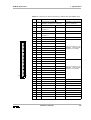
Table of Contents
Table of Contents
Page
Table of Contents . . . . . . . . . . . . . . . . . . . . . . . . . . . . . . . . . . . . . . . . . . . . . . . . . . . . . . . . . . . . . . . . I
List of Tables . . . . . . . . . . . . . . . . . . . . . . . . . . . . . . . . . . . . . . . . . . . . . . . . . . . . . . . . . . . . . . . . . . VI
List of Figures. . . . . . . . . . . . . . . . . . . . . . . . . . . . . . . . . . . . . . . . . . . . . . . . . . . . . . . . . . . . . . . . VIII
Scope of Delivery . . . . . . . . . . . . . . . . . . . . . . . . . . . . . . . . . . . . . . . . . . . . . . . . . . . . . . . . . . . . . . IX
Options . . . . . . . . . . . . . . . . . . . . . . . . . . . . . . . . . . . . . . . . . . . . . . . . . . . . . . . . . . . . . . . . . . . . . . IX
Related Products . . . . . . . . . . . . . . . . . . . . . . . . . . . . . . . . . . . . . . . . . . . . . . . . . . . . . . . . . . . . . . . . X
Conventions . . . . . . . . . . . . . . . . . . . . . . . . . . . . . . . . . . . . . . . . . . . . . . . . . . . . . . . . . . . . . . . . . . XI
How to Use this Manual . . . . . . . . . . . . . . . . . . . . . . . . . . . . . . . . . . . . . . . . . . . . . . . . . . . . . . . . XIII
1 Specification . . . . . . . . . . . . . . . . . . . . . . . . . . . . . . . . . . . . . . . . . . . . . . . . . . . . . . . . . . . . . . . . . . . 1
1.1
Distinguishing Features . . . . . . . . . . . . . . . . . . . . . . . . . . . . . . . . . . . . . . . . . . . . . . . . . . . . . . . 1
1.2
General Description. . . . . . . . . . . . . . . . . . . . . . . . . . . . . . . . . . . . . . . . . . . . . . . . . . . . . . . . . . 3
1.3
Technical Details . . . . . . . . . . . . . . . . . . . . . . . . . . . . . . . . . . . . . . . . . . . . . . . . . . . . . . . . . . . . 7
1.3.1
CPUs . . . . . . . . . . . . . . . . . . . . . . . . . . . . . . . . . . . . . . . . . . . . . . . . . . . . . . . . . . . . . . 7
1.3.2
RAM . . . . . . . . . . . . . . . . . . . . . . . . . . . . . . . . . . . . . . . . . . . . . . . . . . . . . . . . . . . . . . 9
1.3.3
Basic EPROM . . . . . . . . . . . . . . . . . . . . . . . . . . . . . . . . . . . . . . . . . . . . . . . . . . . . . . 10
1.3.4
User EPROM . . . . . . . . . . . . . . . . . . . . . . . . . . . . . . . . . . . . . . . . . . . . . . . . . . . . . . 10
1.3.5
Graphics Interface . . . . . . . . . . . . . . . . . . . . . . . . . . . . . . . . . . . . . . . . . . . . . . . . . . . 11
1.3.6
Keyboard Interface . . . . . . . . . . . . . . . . . . . . . . . . . . . . . . . . . . . . . . . . . . . . . . . . . . 13
1.3.7
Ethernet Interface . . . . . . . . . . . . . . . . . . . . . . . . . . . . . . . . . . . . . . . . . . . . . . . . . . . 13
1.3.8
SCSI Interface . . . . . . . . . . . . . . . . . . . . . . . . . . . . . . . . . . . . . . . . . . . . . . . . . . . . . . 13
1.3.9
Serial I/O . . . . . . . . . . . . . . . . . . . . . . . . . . . . . . . . . . . . . . . . . . . . . . . . . . . . . . . . . . 13
1.3.10
Parallel I/O . . . . . . . . . . . . . . . . . . . . . . . . . . . . . . . . . . . . . . . . . . . . . . . . . . . . . . . . 14
1.3.11
CIO Counters/ Timers . . . . . . . . . . . . . . . . . . . . . . . . . . . . . . . . . . . . . . . . . . . . . . . . 14
1.3.12
Parameter RAM and Real-Time Clock . . . . . . . . . . . . . . . . . . . . . . . . . . . . . . . . . . . 14
1.3.13
Revision EEPROM . . . . . . . . . . . . . . . . . . . . . . . . . . . . . . . . . . . . . . . . . . . . . . . . . . 14
1.3.14
VIC Timer . . . . . . . . . . . . . . . . . . . . . . . . . . . . . . . . . . . . . . . . . . . . . . . . . . . . . . . . . 14
Hardware Manual
I
Table of Contents (Continued)
EUROCOM-27
Page
1.3.15
Watchdog Timer . . . . . . . . . . . . . . . . . . . . . . . . . . . . . . . . . . . . . . . . . . . . . . . . . . . . 15
1.3.16
Status Display . . . . . . . . . . . . . . . . . . . . . . . . . . . . . . . . . . . . . . . . . . . . . . . . . . . . . . 15
1.3.17
Reset . . . . . . . . . . . . . . . . . . . . . . . . . . . . . . . . . . . . . . . . . . . . . . . . . . . . . . . . . . . . . 15
1.3.18
VMEbus Interface . . . . . . . . . . . . . . . . . . . . . . . . . . . . . . . . . . . . . . . . . . . . . . . . . . . 16
1.3.18.1 System Controller . . . . . . . . . . . . . . . . . . . . . . . . . . . . . . . . . . . . . . . . . . . . 16
1.3.18.2 VMEbus Master Interface. . . . . . . . . . . . . . . . . . . . . . . . . . . . . . . . . . . . . . 16
1.3.18.3 VMEbus Slave Interface . . . . . . . . . . . . . . . . . . . . . . . . . . . . . . . . . . . . . . . 16
1.3.19
Interrupt Sources . . . . . . . . . . . . . . . . . . . . . . . . . . . . . . . . . . . . . . . . . . . . . . . . . . . . 17
1.3.20
Local Extension Bus . . . . . . . . . . . . . . . . . . . . . . . . . . . . . . . . . . . . . . . . . . . . . . . . . 17
1.3.21
Software. . . . . . . . . . . . . . . . . . . . . . . . . . . . . . . . . . . . . . . . . . . . . . . . . . . . . . . . . . . 17
1.3.22
Connectors. . . . . . . . . . . . . . . . . . . . . . . . . . . . . . . . . . . . . . . . . . . . . . . . . . . . . . . . . 19
1.4
Compatibility to the EUROCOM-17 . . . . . . . . . . . . . . . . . . . . . . . . . . . . . . . . . . . . . . . . . . . . 28
1.5
Definition of Board Parameters . . . . . . . . . . . . . . . . . . . . . . . . . . . . . . . . . . . . . . . . . . . . . . . . 29
1.5.1
VMEbus. . . . . . . . . . . . . . . . . . . . . . . . . . . . . . . . . . . . . . . . . . . . . . . . . . . . . . . . . . . 29
1.5.2
LEB . . . . . . . . . . . . . . . . . . . . . . . . . . . . . . . . . . . . . . . . . . . . . . . . . . . . . . . . . . . . . . 30
1.5.3
Ethernet . . . . . . . . . . . . . . . . . . . . . . . . . . . . . . . . . . . . . . . . . . . . . . . . . . . . . . . . . . . 30
1.5.4
SCSI. . . . . . . . . . . . . . . . . . . . . . . . . . . . . . . . . . . . . . . . . . . . . . . . . . . . . . . . . . . . . . 30
1.5.5
Serial I/O . . . . . . . . . . . . . . . . . . . . . . . . . . . . . . . . . . . . . . . . . . . . . . . . . . . . . . . . . . 31
1.5.6
Parallel I/O . . . . . . . . . . . . . . . . . . . . . . . . . . . . . . . . . . . . . . . . . . . . . . . . . . . . . . . . 31
1.5.7
Video I/O . . . . . . . . . . . . . . . . . . . . . . . . . . . . . . . . . . . . . . . . . . . . . . . . . . . . . . . . . . 31
1.5.8
MTBF Values . . . . . . . . . . . . . . . . . . . . . . . . . . . . . . . . . . . . . . . . . . . . . . . . . . . . . . 31
1.5.9
Environmental Conditions. . . . . . . . . . . . . . . . . . . . . . . . . . . . . . . . . . . . . . . . . . . . . 32
1.5.10
Power Requirements . . . . . . . . . . . . . . . . . . . . . . . . . . . . . . . . . . . . . . . . . . . . . . . . . 32
2 Installation . . . . . . . . . . . . . . . . . . . . . . . . . . . . . . . . . . . . . . . . . . . . . . . . . . . . . . . . . . . . . . . . . . . 33
2.1
II
Introduction . . . . . . . . . . . . . . . . . . . . . . . . . . . . . . . . . . . . . . . . . . . . . . . . . . . . . . . . . . . . . . . 33
2.1.1
Board Installation . . . . . . . . . . . . . . . . . . . . . . . . . . . . . . . . . . . . . . . . . . . . . . . . . . . 33
2.1.2
Serial Interface Level Converter (SILC) . . . . . . . . . . . . . . . . . . . . . . . . . . . . . . . . . . 34
2.1.3
Installation Parallel I/O . . . . . . . . . . . . . . . . . . . . . . . . . . . . . . . . . . . . . . . . . . . . . . . 34
2.1.4
Ethernet Installation . . . . . . . . . . . . . . . . . . . . . . . . . . . . . . . . . . . . . . . . . . . . . . . . . 35
Hardware Manual
EUROCOM-27
Table of Contents (Continued)
Page
2.1.5
Pure 8-bit SCSI Installation . . . . . . . . . . . . . . . . . . . . . . . . . . . . . . . . . . . . . . . . . . . 35
2.1.6
Pure 16-bit SCSI Installation . . . . . . . . . . . . . . . . . . . . . . . . . . . . . . . . . . . . . . . . . . 35
2.1.7
Mixed 8/16 bit SCSI Installation . . . . . . . . . . . . . . . . . . . . . . . . . . . . . . . . . . . . . . . 35
2.2
Default Board Setting . . . . . . . . . . . . . . . . . . . . . . . . . . . . . . . . . . . . . . . . . . . . . . . . . . . . . . . 37
2.3
Jumpers and Switches . . . . . . . . . . . . . . . . . . . . . . . . . . . . . . . . . . . . . . . . . . . . . . . . . . . . . . . 40
2.3.1
Digclk Invertion (J1201). . . . . . . . . . . . . . . . . . . . . . . . . . . . . . . . . . . . . . . . . . . . . . 40
2.3.2
Enable TTL Video (J1202) . . . . . . . . . . . . . . . . . . . . . . . . . . . . . . . . . . . . . . . . . . . . 40
2.3.3
Watchdog Period (J1401) . . . . . . . . . . . . . . . . . . . . . . . . . . . . . . . . . . . . . . . . . . . . . 41
2.3.4
Flash EPROM Programming Voltage (J1601) . . . . . . . . . . . . . . . . . . . . . . . . . . . . . 41
2.3.5
Pin 1 Connection of EPROM (J1605). . . . . . . . . . . . . . . . . . . . . . . . . . . . . . . . . . . . 41
2.3.6
EEPROM Write Enable (J1702) . . . . . . . . . . . . . . . . . . . . . . . . . . . . . . . . . . . . . . . . 41
2.3.7
VMEbus Interrupts for Secondary CPU (J1703) . . . . . . . . . . . . . . . . . . . . . . . . . . . 42
2.3.8
Switches . . . . . . . . . . . . . . . . . . . . . . . . . . . . . . . . . . . . . . . . . . . . . . . . . . . . . . . . . .
2.3.8.1 VMEbus Slave Address (S901) . . . . . . . . . . . . . . . . . . . . . . . . . . . . . . . . .
2.3.8.2 Hardware Configuration (S902) . . . . . . . . . . . . . . . . . . . . . . . . . . . . . . . . .
2.3.8.3 System Controller Switch (S3) . . . . . . . . . . . . . . . . . . . . . . . . . . . . . . . . . .
42
43
44
44
3 Programmers Reference . . . . . . . . . . . . . . . . . . . . . . . . . . . . . . . . . . . . . . . . . . . . . . . . . . . . . . . . 45
3.1
Address Map . . . . . . . . . . . . . . . . . . . . . . . . . . . . . . . . . . . . . . . . . . . . . . . . . . . . . . . . . . . . . . 45
3.2
DRAM . . . . . . . . . . . . . . . . . . . . . . . . . . . . . . . . . . . . . . . . . . . . . . . . . . . . . . . . . . . . . . . . . . . 47
3.2.1
RAM Access from the Local CPUs . . . . . . . . . . . . . . . . . . . . . . . . . . . . . . . . . . . . . 47
3.2.2
RAM Access from the VMEbus . . . . . . . . . . . . . . . . . . . . . . . . . . . . . . . . . . . . . . . . 47
3.2.3
Address Translation . . . . . . . . . . . . . . . . . . . . . . . . . . . . . . . . . . . . . . . . . . . . . . . . . 48
3.2.4
RAM Mirror . . . . . . . . . . . . . . . . . . . . . . . . . . . . . . . . . . . . . . . . . . . . . . . . . . . . . . . 49
3.2.5
RAM Access from the LEB . . . . . . . . . . . . . . . . . . . . . . . . . . . . . . . . . . . . . . . . . . . 49
3.2.6
RAM Access from ILACC . . . . . . . . . . . . . . . . . . . . . . . . . . . . . . . . . . . . . . . . . . . . 50
Hardware Manual
III
Table of Contents (Continued)
EUROCOM-27
Page
3.3
3.4
VMEbus Interface . . . . . . . . . . . . . . . . . . . . . . . . . . . . . . . . . . . . . . . . . . . . . . . . . . . . . . . . . . 50
3.3.1
System Controller . . . . . . . . . . . . . . . . . . . . . . . . . . . . . . . . . . . . . . . . . . . . . . . . . . . 50
3.3.2
VMEbus Master Interface . . . . . . . . . . . . . . . . . . . . . . . . . . . . . . . . . . . . . . . . . . . . . 51
3.3.2.1 Longword Access to Wordwide Slaves . . . . . . . . . . . . . . . . . . . . . . . . . . . 51
3.3.2.2 Address Modifier Source . . . . . . . . . . . . . . . . . . . . . . . . . . . . . . . . . . . . . . 51
3.3.2.3 Read-Modify-Write Cycles. . . . . . . . . . . . . . . . . . . . . . . . . . . . . . . . . . . . . 51
3.3.2.4 VMEbus Block Transfer Option . . . . . . . . . . . . . . . . . . . . . . . . . . . . . . . . . 52
3.3.2.5 A16 Slave Interface (ICMS, ICGS) . . . . . . . . . . . . . . . . . . . . . . . . . . . . . . 53
Graphics Interface . . . . . . . . . . . . . . . . . . . . . . . . . . . . . . . . . . . . . . . . . . . . . . . . . . . . . . . . . . 55
3.4.1
Video Graphics Address Map . . . . . . . . . . . . . . . . . . . . . . . . . . . . . . . . . . . . . . . . . . 55
3.4.2
Accessing the Internal Register of the Bt445 . . . . . . . . . . . . . . . . . . . . . . . . . . . . . . 58
3.4.3
Address Generator. . . . . . . . . . . . . . . . . . . . . . . . . . . . . . . . . . . . . . . . . . . . . . . . . . . 59
3.4.4
LM1882 Sync Generator . . . . . . . . . . . . . . . . . . . . . . . . . . . . . . . . . . . . . . . . . . . . . . 59
3.4.5
Pixel Model . . . . . . . . . . . . . . . . . . . . . . . . . . . . . . . . . . . . . . . . . . . . . . . . . . . . . . . . 59
3.4.6
Overlay Memory . . . . . . . . . . . . . . . . . . . . . . . . . . . . . . . . . . . . . . . . . . . . . . . . . . . . 60
3.4.7
Video Parameter Restrictions . . . . . . . . . . . . . . . . . . . . . . . . . . . . . . . . . . . . . . . . . . 60
3.4.8
Screen Resolutions . . . . . . . . . . . . . . . . . . . . . . . . . . . . . . . . . . . . . . . . . . . . . . . . . . 61
3.4.9
Digital Video Output . . . . . . . . . . . . . . . . . . . . . . . . . . . . . . . . . . . . . . . . . . . . . . . . . 61
3.5
Ethernet Interface (802.3/10base5) . . . . . . . . . . . . . . . . . . . . . . . . . . . . . . . . . . . . . . . . . . . . . 62
3.6
CIO Counter / Timers . . . . . . . . . . . . . . . . . . . . . . . . . . . . . . . . . . . . . . . . . . . . . . . . . . . . . . . 63
3.7
Serial I/O . . . . . . . . . . . . . . . . . . . . . . . . . . . . . . . . . . . . . . . . . . . . . . . . . . . . . . . . . . . . . . . . . 65
3.7.1
Multi-Protocol Controller (MPC) . . . . . . . . . . . . . . . . . . . . . . . . . . . . . . . . . . . . . . . 65
3.8
Watchdog Timer . . . . . . . . . . . . . . . . . . . . . . . . . . . . . . . . . . . . . . . . . . . . . . . . . . . . . . . . . . . 67
3.9
Keyboard Interface . . . . . . . . . . . . . . . . . . . . . . . . . . . . . . . . . . . . . . . . . . . . . . . . . . . . . . . . . 68
3.10 IOC-2 . . . . . . . . . . . . . . . . . . . . . . . . . . . . . . . . . . . . . . . . . . . . . . . . . . . . . . . . . . . . . . . . . . . . 70
3.10.1
Register Set . . . . . . . . . . . . . . . . . . . . . . . . . . . . . . . . . . . . . . . . . . . . . . . . . . . . . . . . 70
3.11 SCSI Interface . . . . . . . . . . . . . . . . . . . . . . . . . . . . . . . . . . . . . . . . . . . . . . . . . . . . . . . . . . . . . 72
3.11.1
SCSI Controller . . . . . . . . . . . . . . . . . . . . . . . . . . . . . . . . . . . . . . . . . . . . . . . . . . . . . 72
3.12 Status Display . . . . . . . . . . . . . . . . . . . . . . . . . . . . . . . . . . . . . . . . . . . . . . . . . . . . . . . . . . . . . 73
IV
Hardware Manual
EUROCOM-27
Table of Contents (Continued)
Page
3.13 Battery-Backed Parameter RAM and Real-Time Clock . . . . . . . . . . . . . . . . . . . . . . . . . . . . . 74
3.13.1
Parameter RAM . . . . . . . . . . . . . . . . . . . . . . . . . . . . . . . . . . . . . . . . . . . . . . . . . . . . 74
3.13.2
Real-Time Clock . . . . . . . . . . . . . . . . . . . . . . . . . . . . . . . . . . . . . . . . . . . . . . . . . . . . 75
3.14 VIC Timer . . . . . . . . . . . . . . . . . . . . . . . . . . . . . . . . . . . . . . . . . . . . . . . . . . . . . . . . . . . . . . . . 75
3.15 Reset . . . . . . . . . . . . . . . . . . . . . . . . . . . . . . . . . . . . . . . . . . . . . . . . . . . . . . . . . . . . . . . . . . . . 76
3.16 Bus Time-Out . . . . . . . . . . . . . . . . . . . . . . . . . . . . . . . . . . . . . . . . . . . . . . . . . . . . . . . . . . . . . 77
3.17 System Control Register (SCR). . . . . . . . . . . . . . . . . . . . . . . . . . . . . . . . . . . . . . . . . . . . . . . . 78
3.18 Interrupt Sources . . . . . . . . . . . . . . . . . . . . . . . . . . . . . . . . . . . . . . . . . . . . . . . . . . . . . . . . . . . 79
3.18.1
Local Interrupt Sources . . . . . . . . . . . . . . . . . . . . . . . . . . . . . . . . . . . . . . . . . . . . . . . 81
3.18.2
VMEbus Interrupt Sources . . . . . . . . . . . . . . . . . . . . . . . . . . . . . . . . . . . . . . . . . . . . 82
3.19 Secondary CPU Support . . . . . . . . . . . . . . . . . . . . . . . . . . . . . . . . . . . . . . . . . . . . . . . . . . . . . 83
3.19.1
Interrupting the Secondary CPU . . . . . . . . . . . . . . . . . . . . . . . . . . . . . . . . . . . . . . . . 83
3.19.2
Interrupting the Primary CPU . . . . . . . . . . . . . . . . . . . . . . . . . . . . . . . . . . . . . . . . . . 84
3.19.3
VMEbus Interrupts for the Secondary CPU . . . . . . . . . . . . . . . . . . . . . . . . . . . . . . . 85
3.19.4
Cache Coherency and Snooping . . . . . . . . . . . . . . . . . . . . . . . . . . . . . . . . . . . . . . . . 86
3.20 Revision Information. . . . . . . . . . . . . . . . . . . . . . . . . . . . . . . . . . . . . . . . . . . . . . . . . . . . . . . . 87
3.21 Indivisible Cycle Operation. . . . . . . . . . . . . . . . . . . . . . . . . . . . . . . . . . . . . . . . . . . . . . . . . . . 89
3.21.1
Deadlock Resolution . . . . . . . . . . . . . . . . . . . . . . . . . . . . . . . . . . . . . . . . . . . . . . . . . 89
3.21.2
TAS Violation . . . . . . . . . . . . . . . . . . . . . . . . . . . . . . . . . . . . . . . . . . . . . . . . . . . . . . 89
Appendix:
A.1 Mnemonics Chart . . . . . . . . . . . . . . . . . . . . . . . . . . . . . . . . . . . . . . . . . . . . . . . . . . . . . . . . . .
A.1.1 Addressing Capabilities . . . . . . . . . . . . . . . . . . . . . . . . . . . . . . . . . . . . . . . . . . . . . .
A.1.2 Data Transfer Capabilities . . . . . . . . . . . . . . . . . . . . . . . . . . . . . . . . . . . . . . . . . . . .
A.1.3 Glossary . . . . . . . . . . . . . . . . . . . . . . . . . . . . . . . . . . . . . . . . . . . . . . . . . . . . . . . . . .
92
92
92
93
A.2 Address Modifiers on VMEbus. . . . . . . . . . . . . . . . . . . . . . . . . . . . . . . . . . . . . . . . . . . . . . . . 94
A.3 Index . . . . . . . . . . . . . . . . . . . . . . . . . . . . . . . . . . . . . . . . . . . . . . . . . . . . . . . . . . . . . . . . . . . . 95
A.4 References . . . . . . . . . . . . . . . . . . . . . . . . . . . . . . . . . . . . . . . . . . . . . . . . . . . . . . . . . . . . . . . . 97
Technical Action Request Form Sheet
Reader Comments Form Sheet
Hardware Manual
V
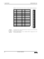
List of Tables
EUROCOM-27
List of Tables
Page
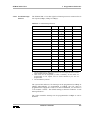
Table 1:
Table 2:
Table 3:
Table 4:
Table 5:
Table 6:
Table 7:
Table 8:
Table 9:
CAS2 Operations on the Various Busses . . . . . . . . . . . . . . . . . . . . . . . . . . . . . . . . . . . . . . . 8
Usable Bandwidth of the RAM . . . . . . . . . . . . . . . . . . . . . . . . . . . . . . . . . . . . . . . . . . . . . . . 9
15-Pin VGA Connector (MONITOR PORT X1201) . . . . . . . . . . . . . . . . . . . . . . . . . . . . . 19
6-Pin Miniature Circular (mini-DIN) Connector (KEYBOARD X2). . . . . . . . . . . . . . . . . 19
6-Pin Telephone Jack Connector CHAN.1(MOUSE/RS 232 PORT X1202) . . . . . . . . . . . 19
15-Pin AUI Connector (ETHERNET X801). . . . . . . . . . . . . . . . . . . . . . . . . . . . . . . . . . . . 20
Pin Assignment of VMEbus Connector (X101) . . . . . . . . . . . . . . . . . . . . . . . . . . . . . . . . . 21
Pin Assignment of Connector X102 . . . . . . . . . . . . . . . . . . . . . . . . . . . . . . . . . . . . . . . . . . 22
Pin Assignment of the 32-bit LEB (X201) . . . . . . . . . . . . . . . . . . . . . . . . . . . . . . . . . . . . . 23
Table 10:
Table 11:
Table 12:
Table 13:
Table 14:
Table 15:
Table 16:
Table 17:
Table 18:
Table 19:
Pin Assignment of 32-Bit Memory Module Connector (X202) . . . . . . . . . . . . . . . . . . . . . 24
50-Pin I/O Connector X102 (on ADAP-200 and ADAP-220) . . . . . . . . . . . . . . . . . . . . . . 25
SCSI Connector 8-bit X103 (on ADAP-200 and ADAP-220) . . . . . . . . . . . . . . . . . . . . . . 26
SCSI Connector 16-bit X107 (on ADAP-220) . . . . . . . . . . . . . . . . . . . . . . . . . . . . . . . . . . 27
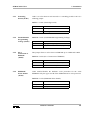
Default Settings . . . . . . . . . . . . . . . . . . . . . . . . . . . . . . . . . . . . . . . . . . . . . . . . . . . . . . . . . . 37
J1201 (Digclk Invertion) . . . . . . . . . . . . . . . . . . . . . . . . . . . . . . . . . . . . . . . . . . . . . . . . . . . 40
J1202 (Enable TTL Video Outputs) . . . . . . . . . . . . . . . . . . . . . . . . . . . . . . . . . . . . . . . . . . 40
J1401 (Watchdog Period) . . . . . . . . . . . . . . . . . . . . . . . . . . . . . . . . . . . . . . . . . . . . . . . . . . 41
J1601 (Flash EPROM Programming Voltage) . . . . . . . . . . . . . . . . . . . . . . . . . . . . . . . . . . 41
J1605 (Pin 1 Connection of EPROM) . . . . . . . . . . . . . . . . . . . . . . . . . . . . . . . . . . . . . . . . . 41
Table 20:
Table 21:
Table 22:
Table 23:
Table 24:
Table 25:
Table 26:
Table 27:
Table 28:
Table 29:
J1702 (EEPROM Write Enable) . . . . . . . . . . . . . . . . . . . . . . . . . . . . . . . . . . . . . . . . . . . . . 41
J1703 (VMEbus Interrupts for Secondary CPU). . . . . . . . . . . . . . . . . . . . . . . . . . . . . . . . . 42
Hex Switch S901 (VMEbus Slave Address) . . . . . . . . . . . . . . . . . . . . . . . . . . . . . . . . . . . . 43
Hex Switch S902 (Hardware Configuration) . . . . . . . . . . . . . . . . . . . . . . . . . . . . . . . . . . . 44
Hex Switch S902 (Hardware Configuration) . . . . . . . . . . . . . . . . . . . . . . . . . . . . . . . . . . . 44
Address Assignment of EUROCOM-27 . . . . . . . . . . . . . . . . . . . . . . . . . . . . . . . . . . . . . . . 45
Local I/O Address Assignment for EUROCOM-27 . . . . . . . . . . . . . . . . . . . . . . . . . . . . . . 46
Slave Base Address Register and Slave Mask Register Layout . . . . . . . . . . . . . . . . . . . . . 47
Enable Slave Register Layout . . . . . . . . . . . . . . . . . . . . . . . . . . . . . . . . . . . . . . . . . . . . . . . 48
Intercommunication Register Location on VMEbus . . . . . . . . . . . . . . . . . . . . . . . . . . . . . . 54
Table 30:
Table 31:
Table 32:
Table 33:
Table 34:
Video Address Map . . . . . . . . . . . . . . . . . . . . . . . . . . . . . . . . . . . . . . . . . . . . . . . . . . . . . . . 55
Register of Bt445 . . . . . . . . . . . . . . . . . . . . . . . . . . . . . . . . . . . . . . . . . . . . . . . . . . . . . . . . . 56
Register of Address and Sync Generator. . . . . . . . . . . . . . . . . . . . . . . . . . . . . . . . . . . . . . . 58
Screen Resolutions. . . . . . . . . . . . . . . . . . . . . . . . . . . . . . . . . . . . . . . . . . . . . . . . . . . . . . . . 61
Ethernet Controller Address Layout . . . . . . . . . . . . . . . . . . . . . . . . . . . . . . . . . . . . . . . . . . 62
VI
Hardware Manual
EUROCOM-27
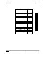
List of Tables (Continued)
Page
Table 35:
Table 36:
Table 37:
Table 38:
Table 39:
Address Assignment of the CIOs . . . . . . . . . . . . . . . . . . . . . . . . . . . . . . . . . . . . . . . . . . . .
SCIO, UCIO Interrupt Level Register. . . . . . . . . . . . . . . . . . . . . . . . . . . . . . . . . . . . . . . . .
Interrupt Level Assignment for SCIO, UCIO and FR. . . . . . . . . . . . . . . . . . . . . . . . . . . . .
Time Constant Values for MPC . . . . . . . . . . . . . . . . . . . . . . . . . . . . . . . . . . . . . . . . . . . . .
Address Assignment of Watchdog Registers . . . . . . . . . . . . . . . . . . . . . . . . . . . . . . . . . . .
63
64
64
65
67
Table 40:
Table 41:
Table 42:
Table 43:
Table 44:
Table 45:
Table 46:
Table 47:
Table 48:
Table 49:
Address Assignment of Keyboard Controller Registers . . . . . . . . . . . . . . . . . . . . . . . . . . .
Keyboard Control/Status Register CSR . . . . . . . . . . . . . . . . . . . . . . . . . . . . . . . . . . . . . . .
Register Map . . . . . . . . . . . . . . . . . . . . . . . . . . . . . . . . . . . . . . . . . . . . . . . . . . . . . . . . . . . .
Address Assignment of SRAM/RTC . . . . . . . . . . . . . . . . . . . . . . . . . . . . . . . . . . . . . . . . .
Address Assignment of the Real-Time Clock . . . . . . . . . . . . . . . . . . . . . . . . . . . . . . . . . . .
Reset Conditions . . . . . . . . . . . . . . . . . . . . . . . . . . . . . . . . . . . . . . . . . . . . . . . . . . . . . . . . .
System Control Register Layout (System CIO) . . . . . . . . . . . . . . . . . . . . . . . . . . . . . . . . .
VIC Interrupt Priority Scheme . . . . . . . . . . . . . . . . . . . . . . . . . . . . . . . . . . . . . . . . . . . . . .
Local Interrupt Sources . . . . . . . . . . . . . . . . . . . . . . . . . . . . . . . . . . . . . . . . . . . . . . . . . . . .
CPU2CON As Seen by Primary CPU . . . . . . . . . . . . . . . . . . . . . . . . . . . . . . . . . . . . . . . . .
68
69
70
74
75
76
78
80
81
84
Table 50:
Table 51:
Table 52:
Table 53:
Table 54:
Table 55:
CPU2CON As Seen by Secondary CPU . . . . . . . . . . . . . . . . . . . . . . . . . . . . . . . . . . . . . . .
Snoop Control Register Layout for EUROCOM-27 . . . . . . . . . . . . . . . . . . . . . . . . . . . . .
Snoop Control Encoding for EUROCOM-27 . . . . . . . . . . . . . . . . . . . . . . . . . . . . . . . . . . .
IOC-2 Control Register at $FEC7.00A8 . . . . . . . . . . . . . . . . . . . . . . . . . . . . . . . . . . . . . . .
I2C Control Register Layout . . . . . . . . . . . . . . . . . . . . . . . . . . . . . . . . . . . . . . . . . . . . . . . .
Address Map of the Serial EEPROM . . . . . . . . . . . . . . . . . . . . . . . . . . . . . . . . . . . . . . . . .
85
86
86
87
88
88
Hardware Manual
VII
List of Figures
EUROCOM-27
List of Figures
Page
Figure 1:
Figure 2:
Figure 3:
Figure 4:
Figure 5:
Figure 6:
Figure 7:
Figure 8:
VIII
Block Diagram. . . . . . . . . . . . . . . . . . . . . . . . . . . . . . . . . . . . . . . . . . . . . . . . . . . . . . . . . . . . 3
Overlay Pixel Data Configuration . . . . . . . . . . . . . . . . . . . . . . . . . . . . . . . . . . . . . . . . . . . . 11
Graphic Interface Building Blocks . . . . . . . . . . . . . . . . . . . . . . . . . . . . . . . . . . . . . . . . . . . 12
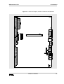
Installation Diagram . . . . . . . . . . . . . . . . . . . . . . . . . . . . . . . . . . . . . . . . . . . . . . . . . . . . . . 36
Location of Jumpers (Bottom View) . . . . . . . . . . . . . . . . . . . . . . . . . . . . . . . . . . . . . . . . . 38
Location of Jumpers, Interface Connectors and Switches. . . . . . . . . . . . . . . . . . . . . . . . . . 39
Switches S901 to S4 . . . . . . . . . . . . . . . . . . . . . . . . . . . . . . . . . . . . . . . . . . . . . . . . . . . . . . 42
Pixel Model . . . . . . . . . . . . . . . . . . . . . . . . . . . . . . . . . . . . . . . . . . . . . . . . . . . . . . . . . . . . . 60
Hardware Manual
EUROCOM-27
Scope of Delivery / Options
Scope of Delivery
Description:
Order No.:
EUROCOM-27
Single 68060, 50 MHz, VME-32
SCSI, Ethernet, Graphics, 32 MB
V-E27.-A139
EUROCOM-27
Single 68060, 50 MHz, VME-32
SCSI, Ethernet, Graphics, 8 MB
V-E27.-A113
EUROCOM-27
Double 68060, 50 MHz, VME-32
SCSI, Ethernet, Graphics, 32 MB
V-E27.-A239
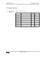
Options
Description:
Order No.:
VIC-64
instead of VIC-32
i
V-E17.-Z001
The last letter of the order numbers refers to the hardware revision and is
subject to changes. Please contact ELTEC for information about valid
order numbers.
Example:
V-E16.-B105
Revision number, subject to change!
Hardware Manual
IX
Related Products
EUROCOM-27
Related Products
Description:
Order No.:
Documentation:
Hardware Manual EUROCOM-27
V-E27.-A990
Service Manual EUROCOM-27 including:
V-E27.-A991
Software Manual RMon (W-FIRM-A209)
Hardware Manual CONV-300 (V-CONV-A993)
LEB Specification (V-LEB.-A990)
IOC-2 Data Sheet (V-DTBT-A924)
MK48T02/12 (V-DTBT-A907)
Z8536 (V-DTBT-A908)
VIC068 (V-DTBT-B914)
NCR53C720 (V-DTBT-A926)
CL-CD2401 (V-DTBT-A923)
ILACC AM79C900 (V-DTBT-A925)
BT445 (V-DTBT-A933)
Hardware:
i
ADAP: to adapt signals on P2 to
SCSI (8-bit) and I/O signals
V-ADAP-A200
ADAP: to connect AT-keyboard to
PS/2 compatible connector
V-ADAP-A210
ADAP: to adapt signals on P2 to
SCSI (16-bit) and I/O signals
V-ADAP-A220
CONV: converts I/O signals to 3 * RS 232
and parallel (TTL) or centronics,
incl. 50-pin ribbon cable
V-CONV-B300
CONV: Cheapernet/10BaseT MAU
V-CONV-A500
RS 232 SILC
V-SILC-E200
RS 422 SILC
V-SILC-B300
RS 485 SILC
V-SILC-A400
Cable (V.24 for terminal)
V-CABL-A144
The last letter of the order numbers refers to the hardware revision and is
subject to changes. Please contact ELTEC for information about valid
order numbers.
Example:
V-E16.-B105
Revision number, subject to change!
X
Hardware Manual
EUROCOM-27
Conventions
Conventions
If not otherwise specified, addresses are written in hexadecimal notation
and identified by a leading dollar sign ("$").
Signal names preceded by a slash ("/"), indicate that this signal is either
active low or that this signal becomes active with the trailing edge.
b
B
K
M
MHz
bit
byte
kilo, means the factor 400 in hex (1024 decimal)
mega, the multiplication with 100 000 in hex (1 048576 decimal)
1 000 000 Hertz
Board-specific abbreviations:
ASR
AUI
BLT
BTO
CAS2
CLUT
CPU
CPU2CON
CSR
CTS
DAC
DMA
DTE
ESR
FIFO
IACK
ICF
ICGS
ICMS
ILACC
IOC-2
LAN
LEB
LIRQ
MAU
MBAR
Address Substitution Register
Attachment Unit Interface
Block Transfer
Bus Time-out
Compare and Swap 2 Instruction
Color Look-up Table
Central Processing Unit
Secondary CPU Control Register
Control/Status Register
Clear to Send
Digital to Analog Converter
Direct Memory Access
Data Terminal Equipment
Enable Slave Register
First In First Out
Interrupt Acknowledge
Interprocessor Communication Facility
Interprocessor Communication Global Switches
Interprocessor Communication Module Switches
Integrated Local Area Communications Controller
I/O Controller Asic
Local Area Network
Local Extension Bus
Local Interrupt Request
Medium Attachment Unit
Memory Base Address Register
Hardware Manual
XI
Conventions (Continued)
EUROCOM-27
MBLT
MPC
PCB
PLL
RAM
RBF
RMC
RTC
RTS
SBR
SCSI
SCR
SILC
SRAM
SMR
TBE
TTL
VIC
VRAM
VTG
UAT
XII
Multiplexed Block Transfer
Multi-Protocol Controller
Printed Circuit Board
Phase Locked Loop
Random Access Memory
Receive Buffer Full
Read-Modify-Write Cycle
Real-time Clock
Request to Send
Slave Base Address Register
Small Computer Systems Interface
System Control Register
Serial Interface Level Converter
Static RAM
Slave Mask Register
Transmit Buffer Empty
Transistor Transistor Logic
VMEbus Interface Chip
Video RAM
Video Timing Generator
Unaligned Transfer
Hardware Manual
EUROCOM-27
How to Use this Manual
How to Use this Manual
Document Structure
This manual is divided into the following chapters:
Chapter 1 Specification contains a list of distinguishing features, a block
diagram with a general description, a description of the main building
blocks and the board parameters.
Chapter 2 Installation describes the requirements and the step-by-step
installation. A table shows the default settings of jumpers and switches
followed by a detailed description of adjustable functions.
Chapter 3 Programmer Reference shows the address map and describes
the address ranges in detail. Special functions are also described in this
chapter.
The Appendix contains references to additional literature, an index, and a
glossary and necessary extracts of data sheets.
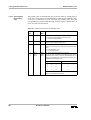
Document Conventions
Font Types:
Font
Use
Helvetica, 8 Pt
Tables and drawings
Helvetica, 10 Pt
Signal names, formulars
Times, italic
Notes
Courier, bold
Program code, function names,
commands
Times, bold
Emphasized text, e.g. headlines
Hardware Manual
XIII
How to Use this Manual (Continued)
EUROCOM-27
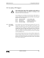
Other Conventions:
i
!
Indicates information that requires close attention.
Indicates critical information that is essential to read.
Indicates information that is imperative to read. Skipping this
material, possibly causes damage to the system.
XIV
Hardware Manual
1 Specification . . . . . . . . . . . . . . . . . . . . . . . . . . . . . . . . . . . . . . . . . . . . . . . . . . . . . . . . . . . . . . . . . . . 1
1.1
Distinguishing Features . . . . . . . . . . . . . . . . . . . . . . . . . . . . . . . . . . . . . . . . . . . . . . . . . . . . . . . 1
1.2
General Description . . . . . . . . . . . . . . . . . . . . . . . . . . . . . . . . . . . . . . . . . . . . . . . . . . . . . . . . . . 3
1.3
Technical Details . . . . . . . . . . . . . . . . . . . . . . . . . . . . . . . . . . . . . . . . . . . . . . . . . . . . . . . . . . . . 7
1.3.1
CPUs . . . . . . . . . . . . . . . . . . . . . . . . . . . . . . . . . . . . . . . . . . . . . . . . . . . . . . . . . . . . . . 7
1.3.2
RAM . . . . . . . . . . . . . . . . . . . . . . . . . . . . . . . . . . . . . . . . . . . . . . . . . . . . . . . . . . . . . . 9
1.3.3
Basic EPROM . . . . . . . . . . . . . . . . . . . . . . . . . . . . . . . . . . . . . . . . . . . . . . . . . . . . . . 10
1.3.4
User EPROM . . . . . . . . . . . . . . . . . . . . . . . . . . . . . . . . . . . . . . . . . . . . . . . . . . . . . . 10
1.3.5
Graphics Interface . . . . . . . . . . . . . . . . . . . . . . . . . . . . . . . . . . . . . . . . . . . . . . . . . . . 11
1.3.6
Keyboard Interface . . . . . . . . . . . . . . . . . . . . . . . . . . . . . . . . . . . . . . . . . . . . . . . . . . 13
1.3.7
Ethernet Interface . . . . . . . . . . . . . . . . . . . . . . . . . . . . . . . . . . . . . . . . . . . . . . . . . . . 13
1.3.8
SCSI Interface . . . . . . . . . . . . . . . . . . . . . . . . . . . . . . . . . . . . . . . . . . . . . . . . . . . . . . 13
1.3.9
Serial I/O . . . . . . . . . . . . . . . . . . . . . . . . . . . . . . . . . . . . . . . . . . . . . . . . . . . . . . . . . . 13
1.3.10
Parallel I/O . . . . . . . . . . . . . . . . . . . . . . . . . . . . . . . . . . . . . . . . . . . . . . . . . . . . . . . . 14
1.3.11
CIO Counters/ Timers . . . . . . . . . . . . . . . . . . . . . . . . . . . . . . . . . . . . . . . . . . . . . . . . 14
1.3.12
Parameter RAM and Real-Time Clock . . . . . . . . . . . . . . . . . . . . . . . . . . . . . . . . . . . 14
1.3.13
Revision EEPROM . . . . . . . . . . . . . . . . . . . . . . . . . . . . . . . . . . . . . . . . . . . . . . . . . . 14
1.3.14
VIC Timer . . . . . . . . . . . . . . . . . . . . . . . . . . . . . . . . . . . . . . . . . . . . . . . . . . . . . . . . . 14
1.3.15
Watchdog Timer . . . . . . . . . . . . . . . . . . . . . . . . . . . . . . . . . . . . . . . . . . . . . . . . . . . . 15
1.3.16
Status Display . . . . . . . . . . . . . . . . . . . . . . . . . . . . . . . . . . . . . . . . . . . . . . . . . . . . . . 15
1.3.17
Reset . . . . . . . . . . . . . . . . . . . . . . . . . . . . . . . . . . . . . . . . . . . . . . . . . . . . . . . . . . . . . 15
1.3.18
VMEbus Interface . . . . . . . . . . . . . . . . . . . . . . . . . . . . . . . . . . . . . . . . . . . . . . . . . . .
1.3.18.1 System Controller . . . . . . . . . . . . . . . . . . . . . . . . . . . . . . . . . . . . . . . . . . . .
1.3.18.2 VMEbus Master Interface . . . . . . . . . . . . . . . . . . . . . . . . . . . . . . . . . . . . .
1.3.18.3 VMEbus Slave Interface. . . . . . . . . . . . . . . . . . . . . . . . . . . . . . . . . . . . . . .
1.3.19
Interrupt Sources . . . . . . . . . . . . . . . . . . . . . . . . . . . . . . . . . . . . . . . . . . . . . . . . . . . . 17
1.3.20
Local Extension Bus . . . . . . . . . . . . . . . . . . . . . . . . . . . . . . . . . . . . . . . . . . . . . . . . . 17
1.3.21
Software . . . . . . . . . . . . . . . . . . . . . . . . . . . . . . . . . . . . . . . . . . . . . . . . . . . . . . . . . . 17
1.3.22
Connectors . . . . . . . . . . . . . . . . . . . . . . . . . . . . . . . . . . . . . . . . . . . . . . . . . . . . . . . . 19
16
16
16
16
1.4
Compatibility to the EUROCOM-17. . . . . . . . . . . . . . . . . . . . . . . . . . . . . . . . . . . . . . . . . . . . 28
1.5
Definition of Board Parameters . . . . . . . . . . . . . . . . . . . . . . . . . . . . . . . . . . . . . . . . . . . . . . . . 29
1
PRELIMINARY
1.5.1
VMEbus. . . . . . . . . . . . . . . . . . . . . . . . . . . . . . . . . . . . . . . . . . . . . . . . . . . . . . . . . . . 29
1.5.2
LEB . . . . . . . . . . . . . . . . . . . . . . . . . . . . . . . . . . . . . . . . . . . . . . . . . . . . . . . . . . . . . . 30
1.5.3
Ethernet . . . . . . . . . . . . . . . . . . . . . . . . . . . . . . . . . . . . . . . . . . . . . . . . . . . . . . . . . . 30
1.5.4
SCSI. . . . . . . . . . . . . . . . . . . . . . . . . . . . . . . . . . . . . . . . . . . . . . . . . . . . . . . . . . . . . . 30
1.5.5
Serial I/O . . . . . . . . . . . . . . . . . . . . . . . . . . . . . . . . . . . . . . . . . . . . . . . . . . . . . . . . . . 31
1.5.6
Parallel I/O . . . . . . . . . . . . . . . . . . . . . . . . . . . . . . . . . . . . . . . . . . . . . . . . . . . . . . . . 31
1.5.7
Video I/O . . . . . . . . . . . . . . . . . . . . . . . . . . . . . . . . . . . . . . . . . . . . . . . . . . . . . . . . . . 31
1.5.8
MTBF Values . . . . . . . . . . . . . . . . . . . . . . . . . . . . . . . . . . . . . . . . . . . . . . . . . . . . . . 31
1.5.9
Environmental Conditions . . . . . . . . . . . . . . . . . . . . . . . . . . . . . . . . . . . . . . . . . . . 32
1.5.10
Power Requirements . . . . . . . . . . . . . . . . . . . . . . . . . . . . . . . . . . . . . . . . . . . . . . . . 32
2 Installation . . . . . . . . . . . . . . . . . . . . . . . . . . . . . . . . . . . . . . . . . . . . . . . . . . . . . . . . . . . . . . . . . . . 33
2.1
2
Introduction . . . . . . . . . . . . . . . . . . . . . . . . . . . . . . . . . . . . . . . . . . . . . . . . . . . . . . . . . . . . . . . 33
2.1.1
Board Installation . . . . . . . . . . . . . . . . . . . . . . . . . . . . . . . . . . . . . . . . . . . . . . . . . . . 33
2.1.2
Serial Interface Level Converter (SILC) . . . . . . . . . . . . . . . . . . . . . . . . . . . . . . . . . . 34
2.1.3
Installation Parallel I/O . . . . . . . . . . . . . . . . . . . . . . . . . . . . . . . . . . . . . . . . . . . . . . . 34
2.1.4
Ethernet Installation . . . . . . . . . . . . . . . . . . . . . . . . . . . . . . . . . . . . . . . . . . . . . . . . . 35
2.1.5
Pure 8-bit SCSI Installation. . . . . . . . . . . . . . . . . . . . . . . . . . . . . . . . . . . . . . . . . . . . 35
2.1.6
Pure 16-bit SCSI Installation. . . . . . . . . . . . . . . . . . . . . . . . . . . . . . . . . . . . . . . . . . . 35
2.1.7
Mixed 8/16 bit SCSI Installation. . . . . . . . . . . . . . . . . . . . . . . . . . . . . . . . . . . . . . . . 35
2.2
Default Board Setting . . . . . . . . . . . . . . . . . . . . . . . . . . . . . . . . . . . . . . . . . . . . . . . . . . . . . . . 37
2.3
Jumpers and Switches . . . . . . . . . . . . . . . . . . . . . . . . . . . . . . . . . . . . . . . . . . . . . . . . . . . . . . . 40
2.3.1
Digclk Invertion (J1201) . . . . . . . . . . . . . . . . . . . . . . . . . . . . . . . . . . . . . . . . . . . . . . 40
2.3.2
Enable TTL Video (J1202) . . . . . . . . . . . . . . . . . . . . . . . . . . . . . . . . . . . . . . . . . . . . 40
2.3.3
Watchdog Period (J1401) . . . . . . . . . . . . . . . . . . . . . . . . . . . . . . . . . . . . . . . . . . . . . 41
2.3.4
Flash EPROM Programming Voltage (J1601) . . . . . . . . . . . . . . . . . . . . . . . . . . . . . 41
2.3.5
Pin 1 Connection of EPROM (J1605). . . . . . . . . . . . . . . . . . . . . . . . . . . . . . . . . . . . 41
2.3.6
EEPROM Write Enable (J1702) . . . . . . . . . . . . . . . . . . . . . . . . . . . . . . . . . . . . . . . . 41
2.3.7
VMEbus Interrupts for Secondary CPU (J1703) . . . . . . . . . . . . . . . . . . . . . . . . . . . 42
2.3.8
Switches. . . . . . . . . . . . . . . . . . . . . . . . . . . . . . . . . . . . . . . . . . . . . . . . . . . . . . . . . . . 42
2.3.8.1 VMEbus Slave Address (S901) . . . . . . . . . . . . . . . . . . . . . . . . . . . . . . . . . 43
2.3.8.2 Hardware Configuration (S902) . . . . . . . . . . . . . . . . . . . . . . . . . . . . . . . . . 44
2.3.8.3 System Controller Switch (S3) . . . . . . . . . . . . . . . . . . . . . . . . . . . . . . . . . . 44
3 Programmers Reference . . . . . . . . . . . . . . . . . . . . . . . . . . . . . . . . . . . . . . . . . . . . . . . . . . . . . . . . 45
3.1
Address Map . . . . . . . . . . . . . . . . . . . . . . . . . . . . . . . . . . . . . . . . . . . . . . . . . . . . . . . . . . . . . . 45
3.2
DRAM . . . . . . . . . . . . . . . . . . . . . . . . . . . . . . . . . . . . . . . . . . . . . . . . . . . . . . . . . . . . . . . . . . . 47
3.3
3.4
3.5
3.2.1
RAM Access from the Local CPUs . . . . . . . . . . . . . . . . . . . . . . . . . . . . . . . . . . . . . 47
3.2.2
RAM Access from the VMEbus . . . . . . . . . . . . . . . . . . . . . . . . . . . . . . . . . . . . . . . . 47
3.2.3
Address Translation . . . . . . . . . . . . . . . . . . . . . . . . . . . . . . . . . . . . . . . . . . . . . . . . . 48
3.2.4
RAM Mirror . . . . . . . . . . . . . . . . . . . . . . . . . . . . . . . . . . . . . . . . . . . . . . . . . . . . . . . 49
3.2.5
RAM Access from the LEB . . . . . . . . . . . . . . . . . . . . . . . . . . . . . . . . . . . . . . . . . . . 49
3.2.6
RAM Access from ILACC . . . . . . . . . . . . . . . . . . . . . . . . . . . . . . . . . . . . . . . . . . . . 50
VMEbus Interface . . . . . . . . . . . . . . . . . . . . . . . . . . . . . . . . . . . . . . . . . . . . . . . . . . . . . . . . . . 50
3.3.1
System Controller . . . . . . . . . . . . . . . . . . . . . . . . . . . . . . . . . . . . . . . . . . . . . . . . . . . 50
3.3.2
VMEbus Master Interface . . . . . . . . . . . . . . . . . . . . . . . . . . . . . . . . . . . . . . . . . . . . .
3.3.2.1 Longword Access to Wordwide Slaves . . . . . . . . . . . . . . . . . . . . . . . . . . .
3.3.2.2 Address Modifier Source . . . . . . . . . . . . . . . . . . . . . . . . . . . . . . . . . . . . . .
3.3.2.3 Read-Modify-Write Cycles . . . . . . . . . . . . . . . . . . . . . . . . . . . . . . . . . . . .
3.3.2.4 VMEbus Block Transfer Option. . . . . . . . . . . . . . . . . . . . . . . . . . . . . . . . .
3.3.2.5 A16 Slave Interface (ICMS, ICGS) . . . . . . . . . . . . . . . . . . . . . . . . . . . . . .
51
51
51
51
52
53
Graphics Interface . . . . . . . . . . . . . . . . . . . . . . . . . . . . . . . . . . . . . . . . . . . . . . . . . . . . . . . . . . 55
3.4.1
Video Graphics Address Map . . . . . . . . . . . . . . . . . . . . . . . . . . . . . . . . . . . . . . . . . . 55
3.4.2
Accessing the Internal Register of the Bt445 . . . . . . . . . . . . . . . . . . . . . . . . . . . . . . 58
3.4.3
Address Generator. . . . . . . . . . . . . . . . . . . . . . . . . . . . . . . . . . . . . . . . . . . . . . . . . . . 59
3.4.4
LM1882 Sync Generator. . . . . . . . . . . . . . . . . . . . . . . . . . . . . . . . . . . . . . . . . . . . . . 59
3.4.5
Pixel Model . . . . . . . . . . . . . . . . . . . . . . . . . . . . . . . . . . . . . . . . . . . . . . . . . . . . . . . . 59
3.4.6
Overlay Memory . . . . . . . . . . . . . . . . . . . . . . . . . . . . . . . . . . . . . . . . . . . . . . . . . . . . 60
3.4.7
Video Parameter Restrictions . . . . . . . . . . . . . . . . . . . . . . . . . . . . . . . . . . . . . . . . . . 60
3.4.8
Screen Resolutions . . . . . . . . . . . . . . . . . . . . . . . . . . . . . . . . . . . . . . . . . . . . . . . . . . 61
3.4.9
Digital Video Output. . . . . . . . . . . . . . . . . . . . . . . . . . . . . . . . . . . . . . . . . . . . . . . . . 61
Ethernet Interface (802.3/10base5) . . . . . . . . . . . . . . . . . . . . . . . . . . . . . . . . . . . . . . . . . . . . . 62
3
PRELIMINARY
3.6
CIO Counter / Timers . . . . . . . . . . . . . . . . . . . . . . . . . . . . . . . . . . . . . . . . . . . . . . . . . . . . . . . 63
3.7
Serial I/O . . . . . . . . . . . . . . . . . . . . . . . . . . . . . . . . . . . . . . . . . . . . . . . . . . . . . . . . . . . . . . . . . 65
3.7.1
Multi-Protocol Controller (MPC) . . . . . . . . . . . . . . . . . . . . . . . . . . . . . . . . . . . . . . . 65
3.8
Watchdog Timer . . . . . . . . . . . . . . . . . . . . . . . . . . . . . . . . . . . . . . . . . . . . . . . . . . . . . . . . . . . 67
3.9
Keyboard Interface . . . . . . . . . . . . . . . . . . . . . . . . . . . . . . . . . . . . . . . . . . . . . . . . . . . . . . . . . 68
3.10 IOC-2 . . . . . . . . . . . . . . . . . . . . . . . . . . . . . . . . . . . . . . . . . . . . . . . . . . . . . . . . . . . . . . . . . . . . 70
3.10.1
Register Set . . . . . . . . . . . . . . . . . . . . . . . . . . . . . . . . . . . . . . . . . . . . . . . . . . . . . . . . 70
3.11 SCSI Interface . . . . . . . . . . . . . . . . . . . . . . . . . . . . . . . . . . . . . . . . . . . . . . . . . . . . . . . . . . . . . 72
3.11.1
SCSI Controller . . . . . . . . . . . . . . . . . . . . . . . . . . . . . . . . . . . . . . . . . . . . . . . . . . . . . 72
3.12 Status Display . . . . . . . . . . . . . . . . . . . . . . . . . . . . . . . . . . . . . . . . . . . . . . . . . . . . . . . . . . . . . 73
3.13 Battery-Backed Parameter RAM and Real-Time Clock . . . . . . . . . . . . . . . . . . . . . . . . . . . . . 74
3.13.1
Parameter RAM. . . . . . . . . . . . . . . . . . . . . . . . . . . . . . . . . . . . . . . . . . . . . . . . . . . . . 74
3.13.2
Real-Time Clock . . . . . . . . . . . . . . . . . . . . . . . . . . . . . . . . . . . . . . . . . . . . . . . . . . . . 75
3.14 VIC Timer . . . . . . . . . . . . . . . . . . . . . . . . . . . . . . . . . . . . . . . . . . . . . . . . . . . . . . . . . . . . . . . . 75
3.15 Reset. . . . . . . . . . . . . . . . . . . . . . . . . . . . . . . . . . . . . . . . . . . . . . . . . . . . . . . . . . . . . . . . . . . . . 76
3.16 Bus Time-Out . . . . . . . . . . . . . . . . . . . . . . . . . . . . . . . . . . . . . . . . . . . . . . . . . . . . . . . . . . . . . 77
3.17 System Control Register (SCR). . . . . . . . . . . . . . . . . . . . . . . . . . . . . . . . . . . . . . . . . . . . . . . . 78
3.18 Interrupt Sources . . . . . . . . . . . . . . . . . . . . . . . . . . . . . . . . . . . . . . . . . . . . . . . . . . . . . . . . . . . 79
3.18.1
Local Interrupt Sources . . . . . . . . . . . . . . . . . . . . . . . . . . . . . . . . . . . . . . . . . . . . . . . 81
3.18.2
VMEbus Interrupt Sources . . . . . . . . . . . . . . . . . . . . . . . . . . . . . . . . . . . . . . . . . . . . 82
3.19 Secondary CPU Support . . . . . . . . . . . . . . . . . . . . . . . . . . . . . . . . . . . . . . . . . . . . . . . . . . . . . 83
3.19.1
Interrupting the Secondary CPU . . . . . . . . . . . . . . . . . . . . . . . . . . . . . . . . . . . . . . . . 83
3.19.2
Interrupting the Primary CPU . . . . . . . . . . . . . . . . . . . . . . . . . . . . . . . . . . . . . . . . . . 84
3.19.3
VMEbus Interrupts for the Secondary CPU . . . . . . . . . . . . . . . . . . . . . . . . . . . . . . . 85
3.19.4
Cache Coherency and Snooping . . . . . . . . . . . . . . . . . . . . . . . . . . . . . . . . . . . . . . . . 86
3.20 Revision Information . . . . . . . . . . . . . . . . . . . . . . . . . . . . . . . . . . . . . . . . . . . . . . . . . . . . . . . . 87
3.21 Indivisible Cycle Operation . . . . . . . . . . . . . . . . . . . . . . . . . . . . . . . . . . . . . . . . . . . . . . . . . . . 89
4
3.21.1
Deadlock Resolution . . . . . . . . . . . . . . . . . . . . . . . . . . . . . . . . . . . . . . . . . . . . . . . . . 89
3.21.2
TAS Violation . . . . . . . . . . . . . . . . . . . . . . . . . . . . . . . . . . . . . . . . . . . . . . . . . . . . . . 89
A.1Mnemonics Chart . . . . . . . . . . . . . . . . . . . . . . . . . . . . . . . . . . . . . . . . . . . . . . . . . . . . . . . . . . . . . 92
A.1.1
Addressing Capabilities . . . . . . . . . . . . . . . . . . . . . . . . . . . . . . . . . . . . . . . . . . . . . . 92
A.1.2
Data Transfer Capabilities . . . . . . . . . . . . . . . . . . . . . . . . . . . . . . . . . . . . . . . . . . . 92
A.1.3
Glossary . . . . . . . . . . . . . . . . . . . . . . . . . . . . . . . . . . . . . . . . . . . . . . . . . . . . . . . . . . 93
A.2Address Modifiers on VMEbus . . . . . . . . . . . . . . . . . . . . . . . . . . . . . . . . . . . . . . . . . . . . . . . . . . 94
5
PRELIMINARY
6
Table 1: CAS2 Operations on the Various Busses . . . . . . . . . . . . . . . . . . . . . . . . . . . . . . . . . . . . . . . 8
Table 2: Usable Bandwidth of the RAM . . . . . . . . . . . . . . . . . . . . . . . . . . . . . . . . . . . . . . . . . . . . . . . 9
Table 3: 15-Pin VGA Connector (MONITOR PORT X1201) . . . . . . . . . . . . . . . . . . . . . . . . . . . . . 19
Table 4: 6-Pin Miniature Circular (mini-DIN) Connector
(KEYBOARD X2)19
Table 5: 6-Pin Telephone Jack Connector CHAN.1
(MOUSE/RS 232 PORT X1202)19
Table 6: 15-Pin AUI Connector (ETHERNET X801) . . . . . . . . . . . . . . . . . . . . . . . . . . . . . . . . . . . 20
Table 7: Pin Assignment of VMEbus Connector (X101) . . . . . . . . . . . . . . . . . . . . . . . . . . . . . . . . . 21
Table 8: Pin Assignment of Connector X102 . . . . . . . . . . . . . . . . . . . . . . . . . . . . . . . . . . . . . . . . . . 22
Table 9: Pin Assignment of the 32-bit LEB (X201) . . . . . . . . . . . . . . . . . . . . . . . . . . . . . . . . . . . . . 23
Table 10: Pin Assignment of 32-Bit Memory Module Connector (X202) . . . . . . . . . . . . . . . . . . . . . 24
Table 11: 50-Pin I/O Connector X102 (on ADAP-200 and ADAP-220) . . . . . . . . . . . . . . . . . . . . . . 25
Table 12: SCSI Connector 8-bit X103 (on ADAP-200 and ADAP-220) . . . . . . . . . . . . . . . . . . . . . . 26
Table 13: SCSI Connector 16-bit X107 (on ADAP-220) . . . . . . . . . . . . . . . . . . . . . . . . . . . . . . . . . . 27
Table 14: Default Settings . . . . . . . . . . . . . . . . . . . . . . . . . . . . . . . . . . . . . . . . . . . . . . . . . . . . . . . . . . 37
Table 15: J1201 (Digclk Invertion) . . . . . . . . . . . . . . . . . . . . . . . . . . . . . . . . . . . . . . . . . . . . . . . . . . . 40
Table 16: J1202 (Enable TTL Video Outputs) . . . . . . . . . . . . . . . . . . . . . . . . . . . . . . . . . . . . . . . . . . 40
Table 17: J1401 (Watchdog Period) . . . . . . . . . . . . . . . . . . . . . . . . . . . . . . . . . . . . . . . . . . . . . . . . . . 41
Table 19: J1605 (Pin 1 Connection of EPROM). . . . . . . . . . . . . . . . . . . . . . . . . . . . . . . . . . . . . . . . . 41
Table 20: J1702 (EEPROM Write Enable) . . . . . . . . . . . . . . . . . . . . . . . . . . . . . . . . . . . . . . . . . . . . . 41
Table 21: J1703 (VMEbus Interrupts for Secondary CPU) . . . . . . . . . . . . . . . . . . . . . . . . . . . . . . . . 42
Table 22: Hex Switch S901 (VMEbus Slave Address) . . . . . . . . . . . . . . . . . . . . . . . . . . . . . . . . . . . . 43
Table 23: Hex Switch S902 (Hardware Configuration) . . . . . . . . . . . . . . . . . . . . . . . . . . . . . . . . . . . 44
Table 25: Address Assignment of EUROCOM-27 . . . . . . . . . . . . . . . . . . . . . . . . . . . . . . . . . . . . . . . 45
Table 26: Local I/O Address Assignment for EUROCOM-27 . . . . . . . . . . . . . . . . . . . . . . . . . . . . . . 46
Table 27: Slave Base Address Register and Slave Mask Register Layout . . . . . . . . . . . . . . . . . . . . . 47
Table 28: Enable Slave Register Layout . . . . . . . . . . . . . . . . . . . . . . . . . . . . . . . . . . . . . . . . . . . . . . . 48
Table 29: Intercommunication Register Location on VMEbus. . . . . . . . . . . . . . . . . . . . . . . . . . . . . . 54
Table 30: Video Address Map . . . . . . . . . . . . . . . . . . . . . . . . . . . . . . . . . . . . . . . . . . . . . . . . . . . . . . . 55
Table 31: Register of Bt445. . . . . . . . . . . . . . . . . . . . . . . . . . . . . . . . . . . . . . . . . . . . . . . . . . . . . . . . . 56
Table 32: Register of Address and Sync Generator . . . . . . . . . . . . . . . . . . . . . . . . . . . . . . . . . . . . . . 58
Table 33: Screen Resolutions . . . . . . . . . . . . . . . . . . . . . . . . . . . . . . . . . . . . . . . . . . . . . . . . . . . . . . . 61
Table 34: Ethernet Controller Address Layout . . . . . . . . . . . . . . . . . . . . . . . . . . . . . . . . . . . . . . . . . . 62
Table 35: Address Assignment of the CIOs . . . . . . . . . . . . . . . . . . . . . . . . . . . . . . . . . . . . . . . . . . . . 63
Table 36: SCIO, UCIO Interrupt Level Register. . . . . . . . . . . . . . . . . . . . . . . . . . . . . . . . . . . . . . . . . 64
Table 37: Interrupt Level Assignment for SCIO, UCIO and FR. . . . . . . . . . . . . . . . . . . . . . . . . . . . . 64
Table 38: Time Constant Values for MPC . . . . . . . . . . . . . . . . . . . . . . . . . . . . . . . . . . . . . . . . . . . . . 65
Table 39: Address Assignment of Watchdog Registers . . . . . . . . . . . . . . . . . . . . . . . . . . . . . . . . . . . 67
Table 40: Address Assignment of Keyboard Controller Registers . . . . . . . . . . . . . . . . . . . . . . . . . . . 68
Table 41: Keyboard Control/Status Register CSR . . . . . . . . . . . . . . . . . . . . . . . . . . . . . . . . . . . . . . . 69
Table 42: Register Map . . . . . . . . . . . . . . . . . . . . . . . . . . . . . . . . . . . . . . . . . . . . . . . . . . . . . . . . . . . . 70
Table 43: Address Assignment of SRAM/RTC . . . . . . . . . . . . . . . . . . . . . . . . . . . . . . . . . . . . . . . . . 74
Table 44: Address Assignment of the Real-Time Clock . . . . . . . . . . . . . . . . . . . . . . . . . . . . . . . . . . . 75
7
Table 45:
Table 46:
Table 47:
Table 48:
Table 49:
Table 50:
Table 51:
Table 52:
Table 53:
Table 54:
Table 55:
8
Reset Conditions . . . . . . . . . . . . . . . . . . . . . . . . . . . . . . . . . . . . . . . . . . . . . . . . . . . . . . . . . 76
System Control Register Layout (System CIO) . . . . . . . . . . . . . . . . . . . . . . . . . . . . . . . . . 78
VIC Interrupt Priority Scheme. . . . . . . . . . . . . . . . . . . . . . . . . . . . . . . . . . . . . . . . . . . . . . . 80
Local Interrupt Sources . . . . . . . . . . . . . . . . . . . . . . . . . . . . . . . . . . . . . . . . . . . . . . . . . . . . 81
CPU2CON As Seen by Primary CPU . . . . . . . . . . . . . . . . . . . . . . . . . . . . . . . . . . . . . . . . . 84
CPU2CON As Seen by Secondary CPU . . . . . . . . . . . . . . . . . . . . . . . . . . . . . . . . . . . . . . . 85
Snoop Control Register Layout for EUROCOM-27 . . . . . . . . . . . . . . . . . . . . . . . . . . . . . 86
Snoop Control Encoding for EUROCOM-27 . . . . . . . . . . . . . . . . . . . . . . . . . . . . . . . . . . . 86
IOC-2 Control Register at $FEC7.00A8 . . . . . . . . . . . . . . . . . . . . . . . . . . . . . . . . . . . . . . . 87
I2C Control Register Layout . . . . . . . . . . . . . . . . . . . . . . . . . . . . . . . . . . . . . . . . . . . . . . . . 88
Address Map of the Serial EEPROM . . . . . . . . . . . . . . . . . . . . . . . . . . . . . . . . . . . . . . . . . 88
Figure 1:
Figure 2:
Figure 3:
Figure 4:
Figure 5:
Figure 6:
Figure 7:
Figure 8:
Block Diagram . . . . . . . . . . . . . . . . . . . . . . . . . . . . . . . . . . . . . . . . . . . . . . . . . . . . . . . . . . . 3
Overlay Pixel Data Configuration . . . . . . . . . . . . . . . . . . . . . . . . . . . . . . . . . . . . . . . . . . . . 11
Graphic Interface Building Blocks . . . . . . . . . . . . . . . . . . . . . . . . . . . . . . . . . . . . . . . . . . . 12
Installation Diagram . . . . . . . . . . . . . . . . . . . . . . . . . . . . . . . . . . . . . . . . . . . . . . . . . . . . . . 36
Location of Jumpers (Bottom View) . . . . . . . . . . . . . . . . . . . . . . . . . . . . . . . . . . . . . . . . . 38
Location of Jumpers, Interface Connectors and Switches . . . . . . . . . . . . . . . . . . . . . . . . . 39
Switches S901 to S4 . . . . . . . . . . . . . . . . . . . . . . . . . . . . . . . . . . . . . . . . . . . . . . . . . . . . . . 42
Pixel Model . . . . . . . . . . . . . . . . . . . . . . . . . . . . . . . . . . . . . . . . . . . . . . . . . . . . . . . . . . . . . 60
9
10
A
Address Map . . . . . . . . . . . . . . . . . . . . . . . . . 45
Address Modifier Source . . . . . . . . . . . . . . . 51
Address Translation . . . . . . . . . . . . . . . . . . . 48
Arbiter . . . . . . . . . . . . . . . . . . . . . . . . . . . . . . 29
ASR . . . . . . . . . . . . . . . . . . . . . . . . . . . . . 48, 71
B
Bandwidth of the RAM . . . . . . . . . . . . . . . . . . 9
basic EPROM . . . . . . . . . . . . . . . . . . . . . . . . 10
baud rate generator . . . . . . . . . . . . . . . . . . . . 65
Block Transfer . . . . . . . . . . . . . . . . . . . . . . . 52
BLT . . . . . . . . . . . . . . . . . . . . . . . . . . . . . . . . 52
Board Installation . . . . . . . . . . . . . . . . . . . . . 33
Bootstrap . . . . . . . . . . . . . . . . . . . . . . . . . . . . 18
BTO . . . . . . . . . . . . . . . . . . . . . . . . . . . . . . . . 50
burst mode . . . . . . . . . . . . . . . . . . . . . . . . . . . . 9
Bus Time-Out . . . . . . . . . . . . . . . . . . . . . . . . 77
C
CIO . . . . . . . . . . . . . . . . . . . . . . . . . . 14, 63, 67
Configuration . . . . . . . . . . . . . . . . . . . . . . . . 18
Connectors . . . . . . . . . . . . . . . . . . . . . . . . . . 19
CPUs . . . . . . . . . . . . . . . . . . . . . . . . . . . . . . . . 7
CSR . . . . . . . . . . . . . . . . . . . . . . . . . . . . . . . . 68
D
dynamic bus sizing . . . . . . . . . . . . . . . . . . . . . 4
E
EBAR0 . . . . . . . . . . . . . . . . . . . . . . . . . . . . . 71
EBAR01 . . . . . . . . . . . . . . . . . . . . . . . . . . . . 71
EDCR0 . . . . . . . . . . . . . . . . . . . . . . . . . . . . . 71
EDCR1 . . . . . . . . . . . . . . . . . . . . . . . . . . . . . 71
EMAR0 . . . . . . . . . . . . . . . . . . . . . . . . . . . . . 71
EMAR01 . . . . . . . . . . . . . . . . . . . . . . . . . . . . 71
ESR . . . . . . . . . . . . . . . . . . . . . . . . . . . . . . . . 47
Ethernet . . . . . . . . . . . . . . . . . . . . . . . . . . 35, 62
Ethernet Interface . . . . . . . . . . . . . . . . . . . . . 13
F
FEPROM . . . . . . . . . . . . . . . . . . . . . . . . . . . . 17
Four Level Arbiter . . . . . . . . . . . . . . . . . . . . 50
G
Graphics Interface . . . . . . . . . . . . . . . . . . 11, 55
11
H
hardware handshake . . . . . . . . . . . . . . . . . . . 13
I
ICF1 decoder . . . . . . . . . . . . . . . . . . . . . . 48, 53
ICF2 decoder . . . . . . . . . . . . . . . . . . . . . . 48, 53
ICR . . . . . . . . . . . . . . . . . . . . . . . . . . . . . . . . 71
interleaved DRAM . . . . . . . . . . . . . . . . . . . . . 4
Interrupt Sources . . . . . . . . . . . . . . . . . . . . . . 17
IOALR . . . . . . . . . . . . . . . . . . . . . . . . . . . . . . 70
IOC-2 . . . . . . . . . . . . . . . . . . . . . . . . . . . . . . . 70
IODCR0 . . . . . . . . . . . . . . . . . . . . . . . . . . . . 70
IODCR1 . . . . . . . . . . . . . . . . . . . . . . . . . . . . 70
IODCR10 . . . . . . . . . . . . . . . . . . . . . . . . . . . 71
IODCR11 . . . . . . . . . . . . . . . . . . . . . . . . . . . 71
IODCR12 . . . . . . . . . . . . . . . . . . . . . . . . . . . 71
IODCR2 . . . . . . . . . . . . . . . . . . . . . . . . . . . . 70
IODCR3 . . . . . . . . . . . . . . . . . . . . . . . . . . . . 70
IODCR4 . . . . . . . . . . . . . . . . . . . . . . . . . . . . 70
IODCR5 . . . . . . . . . . . . . . . . . . . . . . . . . . . . 70
IODCR6 . . . . . . . . . . . . . . . . . . . . . . . . . . . . 70
IODCR7 . . . . . . . . . . . . . . . . . . . . . . . . . . . . 70
IODCR8 . . . . . . . . . . . . . . . . . . . . . . . . . . . . 70
IODCR9 . . . . . . . . . . . . . . . . . . . . . . . . . . . . 70
ITR . . . . . . . . . . . . . . . . . . . . . . . . . . . . . . . . 71
J
JEDEC . . . . . . . . . . . . . . . . . . . . . . . . . . . . . . 10
K
keyboard interface . . . . . . . . . . . . . . . . . . 13, 68
L
Local Extension Bus . . . . . . . . . . . . . . . . . . . 17
Local I/O Address Assignment . . . . . . . . . . . 46
Local Interrupt Sources . . . . . . . . . . . . . . . . . 81
Longword Access to Wordwide Slaves . . . . 51
M
MBAR . . . . . . . . . . . . . . . . . . . . . . . . . . . 48, 71
Multi-Protocol Controller (MPC) . . . . . . . . . 65
P
Parallel I/O . . . . . . . . . . . . . . . . . . . . . . . 14, 34
Parameter RAM . . . . . . . . . . . . . . . . . . . . 14, 74
Power-On Initialization . . . . . . . . . . . . . . . . . 17
PS/2 . . . . . . . . . . . . . . . . . . . . . . . . . . . . . . . . 68
12
R
RAM . . . . . . . . . . . . . . . . . . . . . . . 9, 47, 49, 50
RAM Mirror . . . . . . . . . . . . . . . . . . . . . . . . . 49
RBF . . . . . . . . . . . . . . . . . . . . . . . . . . . . . . . . 68
Read-Modify-Write Cycles . . . . . . . . . . . . . . 51
Real-Time Clock . . . . . . . . . . . . . . . . . . . . . . 74
Reset . . . . . . . . . . . . . . . . . . . . . . . . . . . . 15, 76
RMon . . . . . . . . . . . . . . . . . . . . . . . . . . . . . . 17
S
SBR . . . . . . . . . . . . . . . . . . . . . . . . . . . . . . . . 47
SCSI . . . . . . . . . . . . . . . . . . . . . . . . . . . . . . . 72
SCSI Interface . . . . . . . . . . . . . . . . . . . . . . . . 13
Secondary CPU Support . . . . . . . . . . . . . . . . 83
Serial I/O . . . . . . . . . . . . . . . . . . . . . . . . . 13, 65
SILC . . . . . . . . . . . . . . . . . . . . . . . . . . . . . . . 34
SMR . . . . . . . . . . . . . . . . . . . . . . . . . . . . . . . 47
Status Display . . . . . . . . . . . . . . . . . . . . . 15, 73
SYSCLK . . . . . . . . . . . . . . . . . . . . . . . . . . . . 50
System Control Register . . . . . . . . . . . . . . . . 78
System Controller . . . . . . . . . . . . . . . . . . 16, 50
T
TAS . . . . . . . . . . . . . . . . . . . . . . . . . . . . . . 8, 51
tftp . . . . . . . . . . . . . . . . . . . . . . . . . . . . . . . . . 18
U
User EPROM . . . . . . . . . . . . . . . . . . . . . . . . 10
V
VIC Timer . . . . . . . . . . . . . . . . . . . . . . . . 14, 75
Video Mode . . . . . . . . . . . . . . . . . . . . . . . . . 18
VMEbus . . . . . . . . . . . . . . . . . . . . . . . . . . . . 29
VMEbus Interface . . . . . . . . . . . . . . . . . . . . . 16
VMEbus Interrupt Sources . . . . . . . . . . . . . . 82
VMEbus Master Interface . . . . . . . . . . . . . . . 16
VMEbus Slave Interface . . . . . . . . . . . . . . . . 16
W
Watchdog . . . . . . . . . . . . . . . . . . . . . . . . . . . 67
Watchdog Timer . . . . . . . . . . . . . . . . . . . . . . 15
X
XON / XOFF . . . . . . . . . . . . . . . . . . . . . . . . . 13
13
14
EUROCOM-17-5xx
1 Specification
1 Specification
1.1 Distinguishing Features
•One or two close-coupled 68040 CPUs at 25 MHz, 33 MHz or 40 MHz
•Memory
- Memory module (2, 8, 16, 32, 64 MB) with up to 252 MB RAM for
data/program storage (79 MB/s)
- 2 KB SRAM and RTC for storage of variable system parameters
MK48T12 (MK48T18, DS1644)
- Up to 1 MB user EPROM
- 256 (512) KB basic EPROM for firmware, on-board programmable
- 1 MB VRAM with 32-bit parallel CPU bus port
- 512 KB overlay VRAM
•High resolution graphics interface for MGR, X-WINDOWS and
CAD / CAM applications
- Max. resolution 1152 x 900, 66 Hz (SUN-like)
- Max. dotclock frequency 120 MHz
- 256 simultaneously displayable colors out of 2 24
- 4-bit overlay
- Soft selectable video parameters like dotclock, frame resolution, video
timing, sync polarity
- Vertical and horizontal screen panning
- Interlaced or non-interlaced RS-343A compatible video signal
- 4-bit TTL outputs for flat displays
•Ethernet interface (32-bit ILACC)
•VMEbus Interface Controller:
- System controller and arbiter
- VMEbus interrupter and interrupt handler
- 32-bit BLT 20 MB/s
- Master / slave write posting
- 64-bit MBLT 35 MB/s (VIC064 only)
Hardware Manual
1
1 Specification
EUROCOM-17-5xx
•IOC-2 gate array:
- 68040 to 68020 bus converter
- Dynamic bus sizing for VMEbus and LEB
- Translation of BLT into bursts on '040 bus to allow snooping of BLT
cycles
- Separate arbitration on '040 and '020 bus
- I/O bus interface
- Support for VMEbus UATs to allow snooping
- Interface for a single bytewide EPROM
•Parallel I/O or Centronics port
•Six 16-bit timer / counter
•Four serial ports (RS 232, RS 422, RS 485)
•Smart SCSI-2 (NCR 53C720) interface with burst capability (max.
transfer capacity 20 MB/s) and single-ended 8/16-bit SCSI data bus
•Two rotary switches on front panel for selection of operation modes and
base address
•Status display on front panel
•IBM keyboard interface
•Watchdog timer with watchdog indicator on front panel
•LEB
2
Hardware Manual
EUROCOM-17-5xx
1 Specification
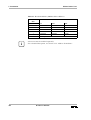
1.2 General Description
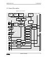
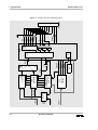
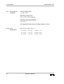
Figure 1: Block Diagram
Aux. CPU
68040
40 MHz
Memory
Module
max. 252 MB
NCR53C720
SCSI
Controller
VMEbus
8/16-bit SCSI-2
X101
CPU
68040
40 MHz
‘040 Bus
Overlay
512K VRAM
1 MB VRAM
I/O Bus
Front
Panel
IOC-2
MUX
CIO
8536
Display
Video
Controller
CLUT
‘020 Bus
Watchdog
Slave Addr.
VMEbus
Controller
VMEbus
Buffer/Count./
Decoder
1M x 8
User EPROM
Operation
Mode
256K x 8
Basic EPROM
VIC
Res/Stat.
32K/2K x 8
NVRAM
RTC
V
G
A
Revision
EEPROM
512 x 8
Keyboard
Controller
Row A
X102
Syscon
Parallel/Timer
8536
Keyboard
RS 232
Serial
Controller
Serial Line
A
U
I
3x
RS 232
Ethernet
Controller
ILACC
Row B
L
E
B
Hardware Manual
3
1 Specification
EUROCOM-17-5xx
The EUROCOM-17-5xx is a highly integrated high-performance singleboard VMEbus computer with graphics display. It is designed to offer as
many features as possible on a single slot VMEbus board. Suitable
intelligent or high integrated components are used to achieve this density
of computing power.
There are two on-board 68040 CPUs, each clocked at 25, 33 or 40 MHz.
On-chip caches for program and data (4 KB capacity each) and the onchip floating-point units allow 35 MIPS/ 5.6 MFLOPS for each CPU.
Additionally, backward compatibility with existing 68000-family
software is guaranteed. Due to the on-chip caches, neither of the CPUs
makes full use of the available bus bandwidth. Thus, parallelizing two
CPUs (closely coupled) puts only a small burden (15%) on processing
speed for most programs.
The main memory is placed on a separate memory module. This easily
allows to expand the memory up to 252 MB without making any changes
necessary at the CPU board. The available memory modules supply
different memory resources such as up to 64 MB DRAM, 4 MB Flash
EPROM and up to 2 MB battery backed SRAM. The main memory can
directly be accessed via the 32-bit processor bus.
The main memory is organized in two banks of interleaved DRAM.
Therefore, burst mode transfers allow 70 MB/s on reads. Due to a buffered
write mechanism, the transfer rate for writes is even bigger (79 MB/s).
This is useful during cache flushes where the CPU may write large
amounts of data.
The major drawback of the 68040 is the deletion of dynamic bus sizing.
This requires 68020/30 applications to be modified if they access word
devices with longword instructions. The longword accesses have to be
split by software into two word accesses which slows down the
performance. Instead of this, the IOC-2 hardware generates the needed
bus cycles if the addressed device acknowledges a smaller data size than
the CPU requested.
4
Hardware Manual
EUROCOM-17-5xx
1 Specification
One of the main design goals of the EUROCOM-17-5xx is efficient use of
the CPU's high speed bus. Thus, the following design rules are
established:
•Use of intelligent peripheral devices which are able to perform tasks
independent from the main CPU (NCR 53C720, CL-CD2401, ILACC).
•Independent 68020-like bus for VMEbus, Ethernet or LEB with separate
arbitration.
•Minimum interference between CPU bus, ‘020 bus and I/O bus.
•Decoupling of VMEbus and CPU bus via FIFO for BLT.
On traditional designs there could only be one bus master on the whole
board at a time. For example, if a BLT was in progress, the CPU was
blocked for the duration of the BLT. At the EUROCOM-17-5xx the CPU
bus is decoupled from the I/O bus.
The display hardware is capable of displaying up to 1152 * 900 pixels at a
rate of 66 Hz, non-interlaced, at a dotclock of 100 MHz. Smaller monitors
with 1024 * 768 or 640 * 480 non-interlaced are also supported. Every
pixel is 1/2/4/8/15/16 bits wide. A color look-up table allows a selection
of 256 simultaneously displayable colors out of a palette of 16 million.
The use of video memories (VRAMs) allows immediate access to the
frame buffer, virtually independent of ongoing display activities.
An additional 512 KB VRAM is implemented on the board to realize a
4-bit graphics overlay. To use the 4-bit graphics overlay, pixel width must
be programmed to 8 bits.
In order to enhance system security, the EUROCOM-17-5xx incorporates
a watchdog timer. It must be retriggered periodically, otherwise the
watchdog generates a reset. After watchdog reset, the watchdog reset LED
on the front panel signals this condition. The watchdog indicator is cleared
only by power-on reset or by triggering the watchdog.
Four serial ports are located on the EUROCOM-17-5xx. One, using a
6-pin shielded RJ11 jack on the front panel, is intended for connection of a
terminal or a mouse. The other three are fed to row A and C of the
VMEbus P2 connector (X102). They can be connected via
ADAP-220/200 and CONV-300 to three 9-pin Sub-D connectors. Two of
the serial lines can be configured to support either RS 232 or RS 422/485
standard via SILCs (Serial Interface Level Converters).
Twelve parallel I/O-lines (X102) can be used either as centronics printer
port or as TTL-level interface (CONV-300).
Hardware Manual
5
1 Specification
EUROCOM-17-5xx
The integrated real-time clock allows the operating system to provide date
and time for revision control. The clock is powered by an internal lithium
battery. 2 (8, 32) KB of battery-backed RAM are used for storage of
system dependent parameters.
An AT-compatible keyboard input (using a 6-pin PS/2 compatible
connector) along with the graphics output provides a PC-type user
interface.
Status display, reset switch, and two hex-code switches are located on the
front panel. The status display indicates the condition of the processor and
watchdog status. The hexadecimal display is an error status display. The
hex-code switches (software readable) are used by the firmware to set up
the operating mode and the VMEbus base address of the board.
The VMEbus interface of the EUROCOM-17-5xx uses the VIC068
VMEbus Interface Controller gate array. Optionally, a VIC064 may be
used which supports D64 multiplexed block transfer according to IEEE
1014 Rev. D.
A 256 (512) K x 8 Flash EPROM holds the firmware. It is on-board
reprogrammable to allow reconfiguration.
Up to 1M x 8 EPROM can be added to the board to hold user firmware.
The on-board Ethernet interface provides connection to most popular local
area networks (LAN).
A sophisticated SCSI-2 (wide) interface is also located on the
EUROCOM-17-5xx. The controller chip is very fast and intelligent so that
it forms a very efficient SCSI interface with max. transfer rates of
20 MB/s.
The on-board local extension bus (LEB) allows easy hardware extension
of the EUROCOM-17-5xx using ELTEC IPINs. The LEB of the
EUROCOM-17-5xx supports dynamic bus sizing.
6
Hardware Manual
EUROCOM-17-5xx
1 Specification
1.3 Technical Details
The EUROCOM-17-5xx consists of the following main blocks:
•CPUs
•RAM Module
•Basic EPROM
•User EPROM
•Graphics Interface
•Keyboard Interface
•Ethernet Interface
•SCSI Interface
•Serial I/0
•Parallel I/O
•CIO Counters / Timers
•Parameter RAM and Real-Time Clock
•Revision EEPROM
•VIC Timer
•Watchdog Timer
•Status Display
•Reset
•VMEbus Interface
•Interrupt Sources
•Local Extension Bus
•Software
•Connectors
1.3.1
CPUs
Equipped with Motorola’s 68040 CPU, the CPUs are clocked with 25, 33
or 40 MHz. All internal bus operations are synchronous to this clock. The
CPUs use burst mode only to access main memory and video RAM.
Although both CPUs are connected mainly in parallel, a distinction into a
primary and a secondary CPU can be made: The primary CPU (CPU1)
receives all system interrupts and is always started first. The secondary
CPU (CPU2) can be released from the reset state afterwards by the
primary CPU (refer to Table 50: ‘CPU2CON As Seen by Primary CPU’).
Hardware Manual
7
1 Specification
EUROCOM-17-5xx
CPU1 handles all interrupts generated by the VIC. CPU2 can interrupt
CPU1 via the interprocessor communication module switch facility of the
VIC. The secondary CPU2 is interrupted by accessing a separate mailbox
location by CPU1, by the LEB or by the VIC timer (refer to Table 50:
‘CPU2CON As Seen by Primary CPU’). Additionally, VMEbus interrupts
can be handled with some restrictions by the secondary CPU. IACK
cycles of CPU1 are always routed to the VIC while those of CPU2 always
use autovector interrupt acknowledge mode.
Non-interruptable read-modify-write cycles (TAS command) are
supported between VMEbus, CPU1, and CPU2. RMC cycles from the
VMEbus to the local RAM are only indivisible when they are byte size.
CAS2 instructions have limited support.
Table 1: CAS2 Operations on the Various Busses
1st op
2nd op
indivisible
local RAM
local RAM
yes
'020 bus (LEB)
local RAM
yes
VMEbus
local RAM
yes
local RAM
'020 bus (LEB)
no
'020 bus (LEB)
'020 bus (LEB)
yes
VMEbus
'020 bus (LEB)
yes
local RAM
VMEbus
no
'020 bus (LEB)
VMEbus
no
VMEbus
VMEbus
yes
The secondary CPU may not be used by the application. All system
functions are served by the primary CPU.
Both CPUs can execute the same code, in case it is reentrant of course.
Each CPU can find out whether it is the primary or secondary CPU by
reading bit 6 of the secondary CPU control register (CPU2CON).
8
Hardware Manual
EUROCOM-17-5xx
1.3.2
RAM
1 Specification
The DRAM and the video RAM are accessed by the following sources:
•CPU1
•CPU2
•SCSI Controller
•Ethernet Controller
•LEB
•VMEbus
Burst mode is supported for accesses of:
•CPU1
•CPU2
•SCSI Controller
•VMEbus BLT
The base address of the DRAM seen from the CPUs is fixed to
$0000.0000. To avoid programming of the MMU, the DRAM and VRAM
are mirrored as non-cacheable RAM.
The base address for accessing the RAM from the VMEbus as well as the
window size is programmable. The on-board firmware uses hex switch
S901 to program the VMEbus address decoder and mask registers.
i
When using A24 addressing, including accesses from the LEB, to access
the EUROCOM-17-5xx RAM, the address translation logic must be
programmed to supply the local addresses A(24) to A(26). In this case
either the video RAM or the DRAM can be reached from VMEbus
(including A32 addressing) but not both (see Section 3.2.3 ‘Address
Translation’).
The following table summarizes the usable bandwidth of the RAM
including precharge and refresh.
Table 2: Usable Bandwidth of the RAM
Bus Clock
40 MHz: (MB/s)
33 MHz: (MB/s)
25 MHz: (MB/s)
DRAM read
70
58
50
DRAM write
79
66
50
VRAM read
53
44
40
VRAM write
53
44
40
Hardware Manual
9
1 Specification
1.3.3
Basic EPROM
EUROCOM-17-5xx
After reset, the basic EPROM is mapped to $0000.0000 so the initial stack
pointer and reset vector can be read. During initialization, it is mapped to
its normal address ($FE80.0000) and the DRAM is located at address
$0000.0000. The basic EPROM is accessed with six wait-states (120 ns
access time) per byte at 40 MHz.
The software in the basic EPROM (RMon) initializes all hardware
according to the parameters in the basic EPROM or the NVRAM
($FEC2.0000).
Reprogramming is possible when the appropriate jumpers are set.
1.3.4
User EPROM
The pin assignment of the 32-pin socket corresponds with the JEDEC
standard. The socket is designed for use with 32-pin EPROMs only. These
EPROM types range from 1 Mb up to 8 Mb (27C010 to 27C080).
The EPROM access time is programmable via IOC-2 register from 4 to 36
wait-states (60 ns to 810 ns maximum access time).
10
Hardware Manual
EUROCOM-17-5xx
1.3.5
Graphics
Interface
1 Specification
The graphics hardware of the EUROCOM-17-5xx is built in the main by a
video sync generator LM1882, a CLUT BT445 and an address generator
which is implemented in a MACH445. The PLD provides the appropriate
control signals for read/write access, transfer cycles and refresh cycles,
too.
The programmable video timing generator allows the implementation of
different screen resolutions and video standards. The pixel clock stream is
fed to a 256 x 8 x 3 CLUT and converted by three DACs into a video
signal (with/without composite sync).
The video RAM consists of two VRAMs building a memory array of
1 MB size and 32-bit parallel/serial port. The VRAM can be accessed by
different bus masters from the 68040 bus (CPU, VMEbus, SCSI, LEB).
Byte, word, longword and burst accesses are possible speeding up
excessive pixel manipulations. Each byte represents one pixel in 8-bit
resolution mode, so that 256 different colors out of a set of 2 24 can be
displayed at the same time. 1/2/4 bits per pixel are also available to speed
up graphics operation.
The overlay RAM is 512 K of size and has the same structure as the video
RAM. Overlay operates with 4 bits per pixel and is only available when
the video RAM operates in 8 bits per pixel. Due to hardware configuration
the overlay RAM is only accessible by word, longword or burst operation.
So, a longword holds the overlay data of four subsequent pixels. The data
of each pixel are held in the lower nibble of each byte in the longword.
The upper nibbles of each byte in the longword are don’t care because
these data lines are not connected to the overlay RAM.
Figure 2: Overlay Pixel Data Configuration
D31
XXXX DDDD
XXXX DDDD
XXXX DDDD
XXXX DDDD
Pixel n
Pixel n+1
Pixel n+2
Pixel n+3
longword boundary
Hardware Manual
11
12
DSF
QSF
Hardware Manual
I/O Bus
/RAS
MHz
25.175
VIDCLK
HSYNC
LM1882
Generator
CBLANK
P(0:63)
VCSYNC
SCLK
2:1
MUX
‘
257
Sync
VRAM Controller/
Address Generator
MACH 445
/CAS
TRA(2:19)
MUX ‘
153
4:1
1 MB
Video RAM
/OE
LA(2:19)
CPU
Bus
LD(0:31)
GA(0:8)
0.5 MB
Overlay RAM
PLL
CLUT
DAC
DAC
DAC
Digital
Output
BT445
VSYNC
HSYNC
B
G
R
BLANK
PCLK
DI
DB
DG
DR
EN
15-Pin Min-D
VGA
1 Specification
EUROCOM-17-5xx
Figure 3: Graphic Interface Building Blocks
EUROCOM-17-5xx
1 Specification
1.3.6
Keyboard
Interface
The EUROCOM-17-5xx keyboard interface supports PS/2 compatible
keyboards. This interface can receive data from and transmit data to the
keyboard under interrupt control. The keyboard interface consists of two
registers: the data register and the control / status register.
1.3.7
Ethernet
Interface
The Ethernet interface is based on the Integrated Local Area
Communications Controller (ILACC - AM79C900).
A main feature of the ILACC and its on-chip DMA channel is the
flexibility and speed of communication. The internal Manchester
Encoder / Decoder of the ILACC is compatible with the IEEE-802.3
specification. Via the AUI connector on the front panel the
EUROCOM-17-5xx is attached to Ethernet (Cheapernet, 10BaseT)
networks.
1.3.8
SCSI Interface
Single-ended 8/16 bit SCSI-2 signals are fed into row A and C of the
VMEbus P2 connector (X102). An ADAP-220 is plugged onto the rear
side of the backplane to interface to standard 8/16-bit SCSI connectors: a
50-pin flat cable connector, and a 68-pin, high density, half pitch
connector (SCSI-2 P cable). The ADAP-220 is also used to interface
between these types of cable, i.e. harddisks with different types of
connectors can be mixed in the system.
For 8-bit SCSI devices also the ADAP-200 can be used.
The NCR53C720 SCSI controller uses its own code fetching and SCSI
data transfer from the on-board DRAM. The processor executes SCSI
SCRIPTS to control the actions on the SCSI and the CPU bus. SCRIPTS
is a specially designed language for easy SCSI protocol handling. It
dramatically reduces the CPU activities. The SCRIPTS processor starts
SCSI I/O operations in approximately 500 ns where traditional intelligent
host adapters require 2-8 ms.
1.3.9
Serial I/O
The EUROCOM-17-5xx offers four serial I/O lines, implemented by one
CL-CD2401 Multi Protocol Controller. CHAN.1 and CHAN.2 are RS 232
two wired handshake interfaces. CHAN.3 and CHAN.4 use removable
serial interface level converters (SILC). As shipped, two RS 232 level
converter SILCs are installed featuring hardware handshake as well as the
XON / XOFF protocol. Additional level converter plug-ins for RS 422
and RS 485 are available.
The baud rate generator is driven by 20 MHz, allowing baud rates from
50 b/s to 64 kb/s.
Hardware Manual
13
1 Specification
1.3.10 Parallel I/O
EUROCOM-17-5xx
There is one 8-bit parallel port with handshake signals on the
EUROCOM-17-5xx. This parallel port is based on a Zilog Z8536 device
(user CIO). The port signals are routed via the VMEbus P2 connector and
the ADAP-220/200 to the CONV-300 board. Three 9-pin Sub-D serial
plugs, a 25-pin Sub-D parallel connector (Centronics printer interface) and
a 26-pin connector for direct access to the CIO pins are installed on the
CONV-300.
The I/O ports of the user CIO features programmable polarity,
programmable direction (bit mode), pulse generators, and programmable
open drain outputs. Four handshake modes, including 3-wire (like
IEEE-488), are selectable. The CIO is also programmable as a 16-vector
interrupt controller.
1.3.11 CIO Counters/
Timers
The EUROCOM-17-5xx offers three independent, programmable 16-bit
counters / timers integrated in the user CIO. They can be used as generalpurpose devices with up to four external access lines per counter / timer
(count input, output, gate, and trigger). Port A and port C lines of the user
CIO are routed to a 26-pin I/O connector on the CONV-300 for user
applications.
1.3.12 Parameter
RAM and RealTime Clock
The real-time clock is designed with the MK48T12 timekeeper RAM. It
combines a 2KBx8 CMOS SRAM (parameter RAM), a bytewide
accessible real-time clock, a crystal, and a long-life lithium battery, all in
one package. Alternatively, a MK48T18 device can be used which offers
8 KB SRAM or a DS1644 device which offers 32Kx8 KB SRAM.
1.3.13 Revision
EEPROM
The revision EEPROM is realized by a 512x8B serial EEPROM which
offers special board revision information. The lower half size of the
EEPROM is programmed by ELTEC and should not be modified by the
user to guarantee board revision consistency. The upper 256 B can be used
by the user to store additional information.
1.3.14 VIC Timer
The VIC contains a timer which can be programmed to output a periodic
wave form on LIRQ2. The available frequencies are 50 Hz, 100 Hz, and
1000 Hz. The VIC timer is typically used as a tick timer for multi-tasking
operating systems.
14
Hardware Manual
EUROCOM-17-5xx
1.3.15 Watchdog
Timer
1 Specification
The watchdog timer monitors the activity of the microprocessor. If the
microprocessor does not access the watchdog timer within the time-out
period of 100 ms or 1.6 s, a reset pulse is generated. After reset, the
watchdog timer is disabled. The normal time-out period of 100 ms/1.6 s
becomes effective after the first access to the watchdog timer.
The left decimal point of the hex display located at the front panel is
illuminated to indicate a watchdog reset. This watchdog indicator is only
cleared by power-up reset, the reset switch, a VMEbus SYSRESET, or a
VIC remote reset.
The state of the watchdog indicator can be read by software using bit PA7
of the system control register located in the system CIO.
1.3.16 Status Display
The EUROCOM-17-5xx features a seven-segment display on the front
panel and displays hexadecimal values from 0 - F.
This status display ($FEC3.0000) is designed as a read / write register and
uses the least significant nibble of the byte.
The right decimal point of the hex display is controlled by PA0 of the
system control register. The right decimal point is used as an initialization
status by the monitor program. After reset the right decimal point is
illuminated. RMon switches the decimal point off before the user program
in the user EPROM is called.
The LED next to the reset button shows the status of the primary CPU. It
is illuminated when the CPU is running and it is off when the CPU is
halted.
1.3.17 Reset
Reset may be initiated by six sources:
•supply voltage drop below 4.75 V or power-up
•reset switch on the front panel
•VMEbus SYSRESET
•VIC remote control reset register
•Watchdog
•CPU RESET instruction
Hardware Manual
15
1 Specification
EUROCOM-17-5xx
1.3.18 VMEbus
Interface
Each EUROCOM-17-5xx board offers VMEbus master and slave
interfaces. Additionally, VMEbus system controller functions are
available via the VMEbus gate array (VIC).
1.3.18.1 System
Controller
The EUROCOM-17-5xx features a full slot-one system controller,
including SYSCLK, SYSRESET, bus time-out, IACK daisy chain driver,
and a four level arbitration circuit. System controller capabilities are
enabled by switch S3 in position 'SC' on the front panel.
1.3.18.2 VMEbus
Master
Interface
The master interface of the EUROCOM-17-5xx board supports 8, 16, and
32-bit data transfer cycles in A32, A24, and A16 addressing modes.
A special feature is provided to support longword accesses from the local
CPU to D16 VMEbus boards (dynamic bus sizing). Two control lines of
the SCR enable longword breaking for the A32 and A24 area.
The VIC chip supplies the VMEbus address modifier signals. This is done
by either routing FC0..2 line to AM0..2, or by driving these signals by an
internal address modifier source register of the VIC ($FEC0.10B7). The
AM3..5 lines are driven depending on the actual data size, or by the
address modifier source register. One output signal of the system control
register is used to control this option.
The EUROCOM-17-5xx supports master / slave block transfer cycles.
Several options within the VIC chip allow the user to generate different
block transfer cycle types.
The overall transfer rate from one EUROCOM-17-5xx to another
EUROCOM-17-5xx is approximately 35 MB/s using D64 block transfer.
1.3.18.3 VMEbus Slave
Interface
The EUROCOM-17-5xx supports A32 and A24 slave access to the
DRAM and an A16 slave interface to access the interprocessor
communication registers. The addresses for all of the slave interfaces are
separately programmable.
For full support of the interprocessor features the EUROCOM-17-5xx has
two A16 slave decoders. One for individual addressing and one for
broadcast addressing of the VIC.
16
Hardware Manual
EUROCOM-17-5xx
1 Specification
1.3.19 Interrupt
Sources
The EUROCOM-17-5xx allows full utilization of both the powerful
VMEbus interrupt structure and the 68040 CPU design.
1.3.20 Local Extension
Bus
The LEB port of the EUROCOM-17-5xx can carry slave-only, masteronly or master-slave boards. The IRQ line of the LEB is connected to
VIC’s LIRQ5 input. The VIC has to be programmed to generate interrupts
on level 2, because only level 2 IACK cycles are routed to the LEB.
1.3.21 Software
The local EUROCOM-17-5xx firmware (RMon) is stored in the on-board
Flash EPROM (FEPROM). RMon provides the basic software layer of the
board. Any operating system or application software is based on the
RMon and uses its functionality:
•Power-On Initialization
•Configuration
•Various Bootstraps
•Externally Callable I/O Functions
•Application Hooks
Power-On Initialization
After RESET or power-on, the local hardware (VIC, serial I/O, CIO,
video, keyboard interface, etc.) must be initialized by the CPU. The
initialization is affected by certain parameters taken either from the onboard NVRAM or from the Flash EPROM (default values). Hex switch
S902 on the front panel selects whether the NVRAM or the default values
are to be used.
The NVRAM parameters are certified by a checksum. If the checksum test
fails, the default parameters are used independent of the switch setting.
After reset or power-on an automatic selftest routine checks the functional
groups of the board and displays its results.
Hardware Manual
17
1 Specification
EUROCOM-17-5xx
Configuration
The configuration program is completely menu driven. The program
interactively shows the configuration parameters and allows their
modification:
•I/O Configuration, e.g.: serial I/O, AT-keyboard, on-board video, baud
rate, etc.
•Video Mode: VGA-Text, VGA-Graphics, SuperVGA, Custom Video
•Bootstrap Configuration
•Internet Address of ILACC
•VMEbus Interface Configuration (VIC Programming)
Various Bootstraps
•OS-9 from SCSI Floppy
•OS-9 from SCSI Harddisk
•OS-9 from SCSI Tape
•OS-9 from ROM/RAM Disk
•Lynx from Tape
•Lynx from Harddisk
•Lynx from Floppy
•tftp-bootstrap from Ethernet including ARP and RARP protocols
•ROMed application bootstrap, suitable as well for VMEbus-downloaded
applications under control of a VMEbus host
External Callable I/O Functions
•Enable/Disable IRQs
•Get Device Status
•Set Device Mode
•Character Raw I/O
•C-like functions getchar, putchar, printf
Application Hooks
Application programs may freely use the externally callable I/O functions
and other information provided in the ‘RMon Fixed Public Location’.
Furthermore, a ROMed application can very easily be started interactively
or automatically after RESET or power-on from RMon. The application
autostart mechanism can be installed simply by setting the respective
bootstrap configuration parameters.
18
Hardware Manual
EUROCOM-17-5xx
1.3.22 Connectors
1 Specification
Table 3: 15-Pin VGA Connector (MONITOR PORT X1201)
Pin
1
Signal (analog)
Red (0.7 VPP / 1 V PP) or Red 3 (TTL)
2
Green (0.7 VPP / 1 VPP ) or Green 3 (TTL)
3
Blue (0.7 VPP / 1 VPP ) or Blue 3 (TTL)
4
nc or Blue 2 (TTL)
5
GND
6
GND
7
GND
8
GND
9
nc
10
GND
11
nc
12
nc or DIGCLK
13
HSync (TTL) prog. (pos./neg.)
14
VSync (TTL) prog. (pos./neg.)
15
nc
15
5
11
1
Table 4: 6-Pin Miniature Circular (mini-DIN) Connector
(KEYBOARD X2)
Pin
Description
1
KBDATA
2
nc
3
GND
4
+5V (fused)
5
KBCLK
6
nc
4
2
6
1
5
3
Table 5: 6-Pin Telephone Jack Connector CHAN.1
(MOUSE/RS 232 PORT X1202)
Pin
Signal
Description
1
DTR
Data Terminal Ready
2
TxD
Transmit Data
3
GND
Signal Ground
4
GND
Signal Ground
5
RxD
Receive Data
6
CTS
Clear to Send
Hardware Manual
1
6
19
1 Specification
EUROCOM-17-5xx
Table 6: 15-Pin AUI Connector (ETHERNET X801)
Pin
20
Signal
Description
1
CI-S
Control In circuit Shield
2
CI-A
Control In circuit A
3
DO-A
Data Out circuit A
4
DI-S
Data In circuit Shield
5
DI-A
Data In circuit A
6
VC
Voltage Common
7
CO-A
Control Out circuit A
8
CO-S
Control Out circuit Shield
9
CI-B
Control Out circuit B
10
DO-B
Data Out circuit B
11
DO-S
Data Out circuit Shield
12
DI-B
Data In circuit B
13
VP
Voltage Plus
14
VS
Voltage Shield
15
CO-B
Control Out circuit B
Hardware Manual
8
15
9
1
EUROCOM-17-5xx
1 Specification
Table 7: Pin Assignment of VMEbus Connector (X101)
Pin
i
Row A
Row B
Row C
1
D00
/BBSY
D08
2
D01
/BCLR
D09
3
D02
/ACFAIL
D10
4
D03
/BG0IN
D11
5
D04
/BG0OUT
D12
6
D05
/BG1IN
D13
7
D06
/BG1OUT
D14
8
D07
/BG2IN
D15
9
GND
/BG2OUT
GND
10
SYSCLK
/BG3IN
/SYSFAIL
11
GND
/BG3OUT
/BERR
12
/DS1
/BR0
/SYSRESET
13
/DS0
/BR1
/LWORD
14
/WRITE
/BR2
AM5
15
GND
/BR3
A23
16
/DTACK
AM0
A22
17
GND
AM1
A21
18
/AS
AM2
A20
19
GND
AM3
A19
20
/IACK
GND
A18
21
/IACKIN
(SERCLK)
A17
22
/IACKOUT
(SERDAT)
A16
23
AM4
GND
A15
24
A07
/IRQ7
A14
25
A06
/IRQ6
A13
26
A05
/IRQ5
A12
27
A04
/IRQ4
A11
28
A03
/IRQ3
A10
29
A02
/IRQ2
A09
30
A01
/IRQ1
A08
31
-12 V
(+5STDBY)
+12 V
32
+5V
+5V
+5V
Signals in parentheses are not connected.
Hardware Manual
21
1 Specification
EUROCOM-17-5xx
Table 8: Pin Assignment of Connector X102
Pin
i
22
Signal Row A
Signal Row B
Signal Row C
1
SCSIDBP1
+5V
SCSIDB1
2
SCSIDB0
GND
SCSIDB3
3
SCSIDB2
Reserved
SCSIDB5
4
SCSIDB4
A24
SCSIDB7
5
SCSIDB6
A25
SCSIDB9
6
SCSIDBP0
A26
SCSIDB11
7
SCSIDB8
A27
SCSIDB13
8
SCSIDB10
A28
SCSIDB15
9
SCSIDB12
A29
CIOPC3
10
SCSIDB14
A30
CIOPC1
11
CIOPC2
A31
CIOPA6
12
CIOPC0
GND
CIOPA4
13
CIOPA7
+5V
CIOPA2
14
CIOPA5
D16
CIOPA0
15
CIOPA3
D17
/SCSIATN
16
CIOPA1
D18
GND
17
GND
D19
/SCSIBSY
18
/SCSIACK
D20
/SCSIRST
19
/SCSIMSG
D21
/SCSISEL
20
/SCSIC/D
D22
/SCSIREQ
21
/SCSII/O
D23
C4GND4
22
C4GND1
GND
C4DTR
23
C4CTS
D24
C4TxD
24
C4RTS
D25
C4RxD
25
C4DCD
D26
C3GND4
26
C3GND1
D27
C3DTR
27
C3CTS
D28
C3TxD
28
C3RTS
D29
C3RxD
29
C3DCD
D30
+5V
30
C2DTR
D31
C2TxD
31
C2CTS
GND
C2RxD
32
C2RTS
+5V
C2DCD
Lines on rows A and C are TTL-level, except Cx signals which have
RS 232C level (SILC-200 used). Pin assignment changes for RS 422/485
configuration. Row B is reserved for 32-bit VMEbus extension.
Hardware Manual
EUROCOM-17-5xx
1 Specification
Table 9: Pin Assignment of the 32-bit LEB (X201)
Pin
i
Row A
Row B
Row C
Row D
Row E
1
GND
A08
A16
A24
Reserved
2
A01
A09
A17
A25
Reserved
3
A02
A10
A18
A26
Reserved
4
A03
A11
A19
A27
Reserved
5
A04
A12
A20
A28
D08
6
A05
A13
A21
A29
D09
7
A06
A14
A22
A30
D10
8
A07
A15
A23
A31
D11
9
D16
D24
FC0
SIZE0
D12
10
D17
D25
FC1
SIZE1
D13
11
D18
D26
FC2
+5V
D14
12
D19
D27
/IRQ
/CPU20
D15
13
D20
D28
/IACK
+12V
D00
14
D21
D29
/RESET
-12V
D01
15
D22
D30
/BR
12VGND
D02
16
D23
D31
/BG
/DSACK0
D03
17
/DS
A00
GND
/HALT
D04
18
R/W
/AS
+5V
+5V
D05
19
/DSACK1
GND
/BGACK
GND
D06
20
/BERR
CLKCPU
/CSEXT
Reserved
D07
Signals in parentheses are not connected.
E
D
C
B
A
1
2
Hardware Manual
19 20
23
1 Specification
EUROCOM-17-5xx
Table 10: Pin Assignment of 32-Bit Memory Module Connector (X202)
Pin
Description
Pin
Description
1A
+12 V
26A
LD5
2A
GND
27A
3A
LA0
4A
Description
Pin
Description
1B
+3V3
26B
LD21
LD6
2B
VCC
27B
LD22
28A
LD7
3B
LA16
28B
LD23
LA1
29A
GND
4B
LA17
29B
VCC
5A
LA2
30A
LD8
5B
LA18
30B
LD24
6A
LA3
31A
LD9
6B
LA19
31B
LD25
7A
LA4
32A
LD10
7B
LA20
32B
LD26
8A
LA5
33A
LD11
8B
LA21
33B
LD27
9A
LA6
34A
LD12
9B
LA22
34B
LD28
10A
LA7
35A
LD13
10B
LA23
35B
LD29
11A
GND
36A
LD14
11B
VCC
36B
LD30
12A
LA8
37A
LD15
12B
LA24
37B
LD31
13A
LA9
38A
GND
13B
LA25
38B
VCC
14A
LA10
39A
/BB
14B
LA26
39B
+3V3
15A
LA11
40A
/TIP
15B
LA27
40B
+3V3
16A
LA12
41A
/TS
16B
LA28
41B
+5VSTDBY
17A
LA13
42A
/LSIZ0
17B
LA29
42B
GND
18A
LA14
43A
/LSIZ1
18B
LA30
43B
GND
19A
LA15
44A
LR/W
19B
LA31
44B
BLCK
20A
GND
45A
/MI
20B
VCC
45B
GND
21A
LD0
46A
GND
21B
LD16
46B
LOCK
22A
LD1
47A
/TA
22B
LD17
47B
/RESET
23A
LD2
48A
/TEA
23B
LD18
48B
RFCLK
24A
LD3
49A
/RAMSEL
24B
LD19
49B
+3V3
25A
LD4
50A
GND
25B
LD20
50B
VCC
24
Pin
Hardware Manual
EUROCOM-17-5xx
1 Specification
Table 11: 50-Pin I/O Connector X102 (on ADAP-200 and ADAP-220)
1
49
2
50
Pin
Dir
Description
Remark
1
8
I/O
Not connected on ADAP-220,
SCSIDB8 - SCSIDB15 on ADAP-200
9
-
10
13
I/O
14
-
15
22
I/O
23
-
+5 V
24
-
Serial Channel 4
GND2
25
-
Serial Channel 4
GND1
26
-
Serial Channel 4
not connected
27
I
Serial Channel 4
CTS
28
O
Serial Channel 4
TXD
29
O
Serial Channel 4
RTS
30
I
Serial Channel 4
RXD
31
-
not connected
32
-
not connected
33
-
Serial Channel 3
GND2
34
-
Serial Channel 3
GND1
35
-
Serial Channel 3
not connected
36
I
Serial Channel 3
CTS
37
O
Serial Channel 3
TXD
38
O
Serial Channel 3
RTS
39
I
Serial Channel 3
RXD
40
-
not connected
41
-
not connected
42
-
Serial Channel 2
GND
43
-
Serial Channel 2
+5 V
44
O
Serial Channel 2
DTR
45
I
Serial Channel 2
CTS
46
O
Serial Channel 2
TXD
47
O
Serial Channel 2
RTS
48
I
Serial Channel 2
RXD
49
-
not connected
50
I
Serial Channel 2
SCSIDB8 - 15 must be left
open on ADAP-200
GND
CIO Port C 3 CIO Port C 0
GND
CIO Port A 7 CIO Port A 0
Hardware Manual
(may be changed if a non
standard level-converter
board SILC is installed)
(may be changed if a non
standard level-converter
board SILC is installed)
fused (300 mA max.)
DCD
25
1 Specification
EUROCOM-17-5xx
Table 12: SCSI Connector 8-bit X103 (on ADAP-200 and ADAP-220)
Pin
i
26
Description
Pin
Description
2
DB0
28
GND
4
DB1
30
GND
6
DB2
32
ATN
8
DB3
34
GND
10
DB4
36
BSY
12
DB5
38
ACK
14
DB6
40
RST
16
DB7
42
MSG
18
DB8
44
SEL
20
GND
46
CIO
22
GND
48
REQ
24
GND
50
I/O
26
TERM-PWR
1
2
49
50
All odd pins of the 50-pin SCSI connector except pin 25 are connected to
ground. Pin 25 is left open.
Pin 26 is connected to +5 V via a Shottky diode to supply power to an
external SCSI terminator.
Hardware Manual
EUROCOM-17-5xx
1 Specification
Table 13: SCSI Connector 16-bit X107 (on ADAP-220)
Pin
Description
Pin
Description
1 - 16
GND
50
GND
17
TERM
51
TERM
18
TERM
52
TERM
19
NC
53
NC
20 - 34
GND
54
GND
35
SCSIDB12
55
/SCSIATN
36
SCSIDB13
56
GND
37
SCSIDB14
57
/SCSIBSY
38
SCSIDB15
58
/SCSIACK
39
SCSIDP1
59
/SCSIRST
40
SCSIDB0
60
/SCSIMSG
41
SCSIDB1
61
/SCSISEL
42
SCSIDB2
62
/SCSIC/D
43
SCSIDB3
63
/SCSIREQ
44
SCSIDB4
64
/SCSII/O
45
SCSIDB5
65
SCSIDB8
46
SCSIDB6
66
SCSIDB9
47
SCSIDB7
67
SCSIDB10
48
SCSIDP0
68
SCSIDB11
49
GND
Hardware Manual
1
35
34
68
27
1 Specification
EUROCOM-17-5xx
1.4 Compatibility to the EUROCOM-17
The EUROCOM-17-5xx is built as an adequate substitute for the
EUROCOM-17-1xx or EUROCOM-17-2xx. Nevertheless, some changes
were necessary:
Differences between EUROCOM-17-5xx and EUROCOM-17-1xx/2xx:
•Address map slightly changed (see Chapter 3 ‘Programmers Reference’).
•The graphics interface has changed. For detailed information, see
Section 3.4 ‘Graphics Interface’.
•4-bit overlay implemented (see Section 1.3.5 ‘Graphics Interface’,
Section 3.4.6 ‘Overlay Memory’).
•Revision EEPROM to save board revision information.
•Programmable interrupt level for system CIO, user CIO, CLCD2401.
•VMEbus interrupt for secondary CPU possible, see Section 2.3.8
‘VMEbus Interrupts for Secondary CPU (J1703)’ for detailed
information.
•Main memory is placed at changeable memory module.
28
Hardware Manual
EUROCOM-17-5xx
1 Specification
1.5 Definition of Board Parameters
1.5.1
VMEbus
•VMEbus interface according to specification ANSI/IEEE
STD 1014-1987 (Rev. D1.4)
•VMEbus Master Capabilities
- MD32
- MRMW8
- BLT
• VMEbus Slave Capabilities:
- SADO32
- SRMW32
- UAT
- BLT
•Arbiter Options
- PRI, RRS
- BTO 4 µs to 480 µs
- SYSCLOCK generation
- BBSY filter
•Requester Options
- Any one of BR(0), BR(1), BR(2) or BR(3)
- Programmable Release when done
(RWD)
- Release-on-request
(ROR)
- Release-on-bus-clear
(ROC)
- Bus capture and hold
(BCAP)
- Programmable fair request timer 2 µs ... 30 µs.
•Interrupt Handler and Generator Capabilities
- Interrupt handler and generator on IRQ1 to IRQ7.
•For Secondary CPU
- Interrupt handler for IRQ 1, 3, 5 or 7 with RORA only
Hardware Manual
29
1 Specification
EUROCOM-17-5xx
•Interrupter Options
- Any one of I(n) where 1 ≤ n ≤ 7.
•Address Range
- programmable extended/standard/short I/O
extended access (A31-A24 and mask)
standard access (A23-A16 and mask)
short I/O (A15 -A8)
- Default: extended access 256 MB, short I/O 256 B
1.5.2
LEB
•LEB Compliance
- D32 4M DBS IRQP IACK DMA A26 NFPM FP
•Master (EUROCOM-17-5xx CPU) Data Transfer Options:
- A32 : D32 : D16 : D8
- 4 MB
•Slave (EUROCOM-17-5xx CPU) Data Transfer Options:
- A32 : D32
- 256 MB (DRAM + VRAM)
•Interrupter Options:
vectored IRQ
•Clock Speed:
- 1/2 CPU clock (12.5 MHz, 16.5 MHz, 20 MHz)
1.5.3
Ethernet
•AUI interface according to 802.3
1.5.4
SCSI
•SCSI-2 wide (8/16 bit single ended)
•Transfer Speed
- asynchronous transfer 5 MB/s (8-bit) 10 MB/s (16-bit)
- synchronous transfer 10 MB/s (8-bit) 20 MB/s (16-bit)
30
Hardware Manual
EUROCOM-17-5xx
1.5.5
Serial I/O
1 Specification
•4 channels (50 b/s - 64 kb/s)
•Keyboard:
- MF2/AT mode
1.5.6
Parallel I/O
•12-bit unbuffered TTL
•CONV-300:
- 12-bit buffered TTL
- Centronics unidirectional
1.5.7
Video I/O
•Dotclock:
- 10 MHz - 120 MHz
•1/2/4/8/15/16 bit/pixel
•CLUT:
- 256 colors out of 2 24
- 3x8-bit DAC
•Video Resolution:
- 640 x 480 - 1152 x 900
•Horizontal Frequencies:
- 31.5 kHz to 70 kHz
•Vertical Frequencies:
- 60 Hz to 70 Hz
1.5.8
MTBF Values
•7756 h (computed after MTL HDBK-217E)
•103930.4 h (realistic value from industry standard experience)
Hardware Manual
31
1 Specification
1.5.9
Environmental
Conditions
EUROCOM-17-5xx
•Storage Temperature:
-35°C to +85°C
•Operating Temperature:
0°C to +60°C (non condensing)
•Maximum Operating Humidity:
85% relative
•Air temperature with forced air cooling of approx. 1 m/sec.
1.5.10 Power
Requirements
32
(with all/max. options; approx.):
+5 VDC
±5 %
- 7.0 A max.
5.0 A typ.
- 0.2 A max.
0.1 A typ.
+12 VDC ±10 %
- 0.2 A max.
0.1 A typ.
-12 VDC ±10 %
Hardware Manual
EUROCOM-17-5xx
2 Installation
2 Installation
2.1 Introduction
•Carefully remove the board from the shipping carton.
- Save the original shipping container and packing material for storing
or reshipping the board.
Avoid touching integrated circuits except in an electrostatic free
environment. Electrostatic discharge can damage circuits or shorten
their lifetime.
•Inspect the board for any shipping damage. If undamaged, the board can
be prepared for system installation.
When unplugging boards from the rack or otherwise handling
boards, do always observe precautions for handling electrostatic
devices.
2.1.1
Board
Installation
The installation of the EUROCOM-17-5xx is not complicated, requiring
only a VGA monitor, an AT-keyboard with PS/2 connector, a power
supply, and a suitably terminated VMEbus backplane. The power supply
must meet the specifications described in Section 1.5 ‘Definition of Board
Parameters’. The processor board requires +5 V supply voltage; ±12 V are
needed for the RS 232 serial interface and the Ethernet interface.
A standard VGA monitor has to be connected to the 15-pin Sub-D female
connector and the keyboard has to be connected to 6-pin female miniature
circular (mini-DIN) connector. Both connectors are located on the front
panel. A standard VGA monitor and a standard PS/2 compatible keyboard
will fit without modification. For connection to an AT-keyboard,
ADAP-210 is available.
Hardware Manual
33
2 Installation
2.1.2
Serial Interface
Level
Converter
(SILC)
EUROCOM-17-5xx
The Serial Interface Level Converter (SILC) modules generally convert
TTL-level signals generated or accepted by the SCC-2 to the appropriate
signal levels for external transmission lines. SILC modules for RS 232C,
RS 422 and RS 485 are available.
The mechanical outline of the SILC modules allows the changeability of
the different SILC modules on the EUROCOM-17-5xx.
•SILC-200 for RS 232
•SILC-300 for RS 422
•SILC-400 for RS 485
The mechanical part of the installation is very easy. First switch off the
VMEbus system and pull the board out of the rack. If a SILC module is
already placed in the connector, remove it carefully. Now plug the new
SILC module into the corresponding connector on the CPU or I/O board.
Consider the polarization of the SILC module. To avoid damage, check
that the pin 1 marked on the back of the SILC fits to pin 1 marked on the
board.
2.1.3
Installation
Parallel I/O
In addition, a 8-bit parallel port with handshake signals is available on the
EUROCOM-17-5xx. The port signals are connected via connector X102
and the ADAP-200/220 to the CONV-300 board. The three 9-pin Sub-D
serial plugs, a 25-pin Sub-D parallel connector to support Centronics
printer interface and a 26-pin connector for direct access to the CIO pins
for user applications are installed on the CONV-300.
The printer port has to be enabled by jumper J1 on the CONV-300 board.
A general 25-pin Sub-D to Centronics printer port cable is used to connect
a parallel printer to the EUROCOM-17-5xx. The printer port supports the
following buffered hardware lines:
D(1:8), /STROBE , /ACK, BUSY , and PE.
For user-defined usage of the CIO parallel ports the printer port has to be
disabled with jumper J1 located on the CONV-300. After that the 26-pin
parallel I/O port supports two CIO parallel ports. For more information
about the CIO, refer to the Z8536 data sheet and the CONV-300 Hardware
Manual.
34
Hardware Manual
EUROCOM-17-5xx
2 Installation
2.1.4
Ethernet
Installation
A standard Ethernet/Cheapernet MAU or a CONV-500 Cheapernet/
10BaseT MAU can be connected via AUI cable to the 15-pin AUI
connector on the front panel of the EUROCOM-17-5xx. The length of the
AUI cable is limited to 50 m. For connections up to about 2 m, flat cable
can also be used. In order to avoid HF radiation, this cable should be
shielded.
2.1.5
Pure 8-bit SCSI
Installation
A 8-bit SCSI bus can be connected to X103 of ADAP-200/220. If the
EUROCOM-17-5xx is located at either end of the SCSI bus, RN601-604
must be installed for signal termination, otherwise RN601-604 must be
removed.
2.1.6
Pure 16-bit
SCSI
Installation
A 16-bit SCSI bus can be connected to X107 of ADAP-220. If the
EUROCOM-17-5xx is located at either end of the SCSI bus, RN601-604
must be installed for signal termination, otherwise RN601-604 must be
removed.
2.1.7
Mixed 8/16 bit
SCSI
Installation
ADAP-220 can be used to build mixed 8/16 bit SCSI bus systems. In this
case X103 and X107 are used. RN601-604 must be removed from the
EUROCOM-17-5xx and two of the resistor networks must be plugged
into RN101-102 sockets of the ADAP-220 (note pin 1 marking of the
networks and the sockets).
Hardware Manual
35
2 Installation
EUROCOM-17-5xx
Figure 4: Installation Diagram
Centronics Port
Status Display
SCSI Port
Slave Address
Operating Mode
System Controller
Reset / Status
Parallel I/O (TTL)
Monitor (VGA) Port
Keyboard
Mouse / Serial (RS 232) Port
RS 232 Port
Ethernet
RS 232 Ports (RS 422, RS 485)
36
Hardware Manual
EUROCOM-17-5xx
2 Installation
2.2 Default Board Setting
Table 14: Default Settings
Jumpers/Switches
Position
Description
J301
1-2
VIC68
J1201
1-2
Digclk, see Section 2.3.1 ‘
Digclk Invertion (J1201)’
J1202
open
TTL graphic outputs disabled, see Section 2.3.2
‘
Enable TTL Video (J1202)’
J1401
closed
J1601
open
No programming voltage for Flash EPROM,
see Section 2.3.4 ‘
Flash EPROM Programming
Voltage (J1601)’
J1605
1-2
See Section 2.3.5 ‘
Pin 1 Connection of EPROM
(J1605)’
J1701
open
Boot from Flash EPROM
J1702
closed
Write enable for serial EEPROM, seeSection 2.3.6
‘
EEPROM Write Enable (J1702)’
J1703
open
No VMEbus IRQs handled by secondary CPU.
(See Section 2.3.8 ‘
VMEbus Interrupts for
Secondary CPU (J1703)’
)
J1801
1-2
See Section 2.3.7 ‘
Snooping of Secondary CPU
(J1801)’
S901
0
VMEbus slave address at $8000.0000, see
Section 2.3.9.1 ‘
VMEbus Slave Address (S901)’
S902
0
Default initialization values, see Section 2.3.9.2
‘
Hardware Configuration (S902)’
SC
System controller enabled, see Section 2.3.9.3
‘
System Controller Switch (S3)’
S3
Watchdog period 100 ms,
‘
Watchdog Period (J1401)’
Hardware Manual
see
Section 2.3.3
37
2 Installation
EUROCOM-17-5xx
Figure 5: Location of Jumpers (Bottom View)
38
Hardware Manual
EUROCOM-17-5xx
2 Installation
Figure 6: Location of Jumpers, Interface Connectors and Switches
Hardware Manual
39
2 Installation
EUROCOM-17-5xx
2.3 Jumpers and Switches
This section lists all features user-selectable by jumpers and switches. For
details, refer to the appropriate descriptions identified in parentheses.
All settings on a dark grey background (
) indicate default settings.
The EUROCOM-17-5xx operates as single board computer in this
configuration.
There are only very few jumpers on the EUROCOM-17-5xx which
typically need no changes after shipping. All other parameters are
software programmable. Since the jumper connections are not changed
easily, it is strongly recommended that these changes are performed by
qualified personal only.
The user should refer to the silkscreen print on the component side of the
EUROCOM-17-5xx for the following guidance on jumper area pin
identification. Pin 1 of every jumper area is marked by a beveled corner
on the silkscreen outline of the jumper. If you see this corner at the left
upper side of the jumper area, then pin 2 is on the right-hand side of pin 1.
Pin 3 can be found on the right of pin 2, and so on. Reaching the end of the
row, counting must be continued beginning on the left-hand side of the
next row.
2.3.1
Digclk
Invertion
(J1201)
J1201 allows to invert the Digclk signal.
Table 15: J1201 (Digclk Invertion)
Jumper J1201
2.3.2
Enable TTL
Video (J1202)
Function
1-2
Digclk
2-3
Inverted Digclk
J1202 is used to enable the TTL video outputs at the VGA connector.
Table 16: J1202 (Enable TTL Video Outputs)
Jumper J1202
40
Function
open
TTL outputs disabled
closed
TTL outputs enabled
Hardware Manual
EUROCOM-17-5xx
2.3.3
Watchdog
Period (J1401)
2 Installation
J1401 is to select between 100 ms and 1.6 s watchdog periods. J1401 is a
soldering jumper.
Table 17: J1401 (Watchdog Period)
2.3.4
2.3.5
Flash EPROM
Programming
Voltage (J1601)
Pin 1
Connection of
EPROM
(J1605)
Jumper J1401
Function
open
Watchdog period 1.6 s
closed
Watchdog period 100 ms
Table 18: J1601 (Flash EPROM Programming Voltage)
Jumper J1601
Function
open
No programming voltage on Flash EPROM
closed
Apply +12 V to Flash EPROM for programming
This jumper allows to select between EPROMs up to 4 Mbit and 8 Mbit.
Table 19: J1605 (Pin 1 Connection of EPROM)
Jumper J1605
2.3.6
EEPROM
Write Enable
(J1702)
Function
1-2
Pin 1 connected to +5 V (< 8 Mbit)
2-3
Pin 1 connected to A19 (8 Mbit)
J1702 enables/disables the hardware write protection for the serial
EEPROM. Only the upper 256 B of the EEPROM can be write protected.
Table 20: J1702 (EEPROM Write Enable)
Jumper J1201
open
closed
Function
Write protection enabled
Write protection disabled
Hardware Manual
41
2 Installation
2.3.7
Snooping of
Secondary CPU
(J1801)
EUROCOM-17-5xx
If snooping of the secondary CPU is enabled via the snoop control register
SNCR, the /MI output of the secondary CPU must be observed (J1801 in
position 2-3).
If snooping of the secondary CPU is disabled or in single processor
systems, /MI of the secondary CPU can be ignored (J1801 in position
1-2).
Table 21: J1801 (Snooping of Secondary CPU)
Jumper J1801
2.3.8
VMEbus
Interrupts for
Secondary CPU
(J1703)
Function
1-2
Ignore /MI of secondary CPU
2-3
Observe /MI of secondary CPU
To enable interrupt handling on the VMEbus by the secondary CPU,
J1703 must be set to the corresponding level. Only one VMEbus interrupt
level can be handled by the secondary CPU! For more information, see
Section 3.19.3 ‘VMEbus Interrupts for the Secondary CPU’.
Table 22: J1703 (VMEbus Interrupts for Secondary CPU)
Jumper J1703
42
Function
5-3
VMEbus interrupt level 7
1-3
VMEbus interrupt level 5
2-4
VMEbus interrupt level 3
6-4
VMEbus interrupt level 1
open
No VMEbus interrupts for secondary CPU
Hardware Manual
EUROCOM-17-5xx
2.3.9
Switches
2 Installation
Two rotary hex switches (S901 and S902), the system controller switch
(S3) and the reset switch (S4) are all located on the front panel. If the
system controller switch (S3) is switched to the 'SC' position, the board
acts as VMEbus system controller.
Figure 7: Switches S901 to S4
Status Display
Hex Switch (S901)
Hex Switch (S902)
System Controller Switch (S3)
Reset Switch (S4)
Both hex switches (S901, S902) are used by RMon for the configuration
setup (see RMon manual).
2.3.9.1 VMEbus Slave
Address (S901)
The upper hex switch (S901) selects the EUROCOM-17-5xx slave
window address. The size of the A32 slave window is normally 256 MB.
This can be changed by the RMon setup menu. The size of the A16 slave
window (used for VIC access) is 256 bytes.
Hardware Manual
43
2 Installation
EUROCOM-17-5xx
Table 23: Hex Switch S901 (VMEbus Slave Address)
Hex Switch
S901
i
44
VMEbus Base Address
A32
A24
A16
F
$F000.0000
disabled
$F000
E
$E000.0000
disabled
$E000
D
$D000.0000
disabled
$D000
.
.
.
.
1
$1000.0000
disabled
$1000
0
Use configuration value
A24 access must be enabled separately.
For a detailed description, see Section 3.2.3 ‘Address Translation’.
Hardware Manual
EUROCOM-17-5xx
2.3.9.2 Hardware
Configuration
(S902)
2 Installation
The lower switch (S902) defines the configuration source and the
operation mode. For switch position 0, 1, RMon enters an interactive
mode. If switch S902 is in position 8 to F, the program located in the user
EPROM is called.
Table 24: Hex Switch S902 (Hardware Configuration)
Hex Switch
S902
i
2.3.9.3 System
Controller
Switch (S3)
Function
0
Hardware configuration from basic EPROM
1
Hardware configuration from SRAM
2
Reserved for ELTEC
3
RMon interactive mode on serial port
4
RMon interactive mode on dual-ported RAM
(local address $C000)
5-7
Reserved for ELTEC
8-F
Hardware configuration from SRAM and start program in user EPROM.
S901 and S902 have no direct influence. A changed position becomes only
effective after the next reset (i.e. the software reads the switches and
programs the appropriate registers).
Table 25: Switch S3 (System Controller Switch)
Hex Switch S3
left
Function
System controller disabled
right 'SC'
System controller enabled
Hardware Manual
45
2 Installation
46
EUROCOM-17-5xx
Hardware Manual
EUROCOM-17-5xx
2 Installation
2 Installation
2.1 Introduction
•Carefully remove the board from the shipping carton.
- Save the original shipping container and packing material for storing
or reshipping the board.
Avoid touching integrated circuits except in an electrostatic free
environment. Electrostatic discharge can damage circuits or shorten
their lifetime.
•Inspect the board for any shipping damage. If undamaged, the board can
be prepared for system installation.
When unplugging boards from the rack or otherwise handling
boards, do always observe precautions for handling electrostatic
devices.
2.1.1
Board
Installation
The installation of the EUROCOM-17-5xx is not complicated, requiring
only a VGA monitor, an AT-keyboard with PS/2 connector, a power
supply, and a suitably terminated VMEbus backplane. The power supply
must meet the specifications described in Section 1.5 ‘Definition of Board
Parameters’. The processor board requires +5 V supply voltage; ±12 V are
needed for the RS 232 serial interface and the Ethernet interface.
A standard VGA monitor has to be connected to the 15-pin Sub-D female
connector and the keyboard has to be connected to 6-pin female miniature
circular (mini-DIN) connector. Both connectors are located on the front
panel. A standard VGA monitor and a standard PS/2 compatible keyboard
will fit without modification. For connection to an AT-keyboard,
ADAP-210 is available.
Hardware Manual
33
2 Installation
2.1.2
Serial Interface
Level
Converter
(SILC)
EUROCOM-17-5xx
The Serial Interface Level Converter (SILC) modules generally convert
TTL-level signals generated or accepted by the SCC-2 to the appropriate
signal levels for external transmission lines. SILC modules for RS 232C,
RS 422 and RS 485 are available.
The mechanical outline of the SILC modules allows the changeability of
the different SILC modules on the EUROCOM-17-5xx.
•SILC-200 for RS 232
•SILC-300 for RS 422
•SILC-400 for RS 485
The mechanical part of the installation is very easy. First switch off the
VMEbus system and pull the board out of the rack. If a SILC module is
already placed in the connector, remove it carefully. Now plug the new
SILC module into the corresponding connector on the CPU or I/O board.
Consider the polarization of the SILC module. To avoid damage, check
that the pin 1 marked on the back of the SILC fits to pin 1 marked on the
board.
2.1.3
Installation
Parallel I/O
In addition, a 8-bit parallel port with handshake signals is available on the
EUROCOM-17-5xx. The port signals are connected via connector X102
and the ADAP-200/220 to the CONV-300 board. The three 9-pin Sub-D
serial plugs, a 25-pin Sub-D parallel connector to support Centronics
printer interface and a 26-pin connector for direct access to the CIO pins
for user applications are installed on the CONV-300.
The printer port has to be enabled by jumper J1 on the CONV-300 board.
A general 25-pin Sub-D to Centronics printer port cable is used to connect
a parallel printer to the EUROCOM-17-5xx. The printer port supports the
following buffered hardware lines:
D(1:8), /STROBE , /ACK, BUSY , and PE.
For user-defined usage of the CIO parallel ports the printer port has to be
disabled with jumper J1 located on the CONV-300. After that the 26-pin
parallel I/O port supports two CIO parallel ports. For more information
about the CIO, refer to the Z8536 data sheet and the CONV-300 Hardware
Manual.
34
Hardware Manual
EUROCOM-17-5xx
2 Installation
2.1.4
Ethernet
Installation
A standard Ethernet/Cheapernet MAU or a CONV-500 Cheapernet/
10BaseT MAU can be connected via AUI cable to the 15-pin AUI
connector on the front panel of the EUROCOM-17-5xx. The length of the
AUI cable is limited to 50 m. For connections up to about 2 m, flat cable
can also be used. In order to avoid HF radiation, this cable should be
shielded.
2.1.5
Pure 8-bit SCSI
Installation
A 8-bit SCSI bus can be connected to X103 of ADAP-200/220. If the
EUROCOM-17-5xx is located at either end of the SCSI bus, RN601-604
must be installed for signal termination, otherwise RN601-604 must be
removed.
2.1.6
Pure 16-bit
SCSI
Installation
A 16-bit SCSI bus can be connected to X107 of ADAP-220. If the
EUROCOM-17-5xx is located at either end of the SCSI bus, RN601-604
must be installed for signal termination, otherwise RN601-604 must be
removed.
2.1.7
Mixed 8/16 bit
SCSI
Installation
ADAP-220 can be used to build mixed 8/16 bit SCSI bus systems. In this
case X103 and X107 are used. RN601-604 must be removed from the
EUROCOM-17-5xx and two of the resistor networks must be plugged
into RN101-102 sockets of the ADAP-220 (note pin 1 marking of the
networks and the sockets).
Hardware Manual
35
2 Installation
EUROCOM-17-5xx
Figure 4: Installation Diagram
Centronics Port
Status Display
SCSI Port
Slave Address
Operating Mode
System Controller
Reset / Status
Parallel I/O (TTL)
Monitor (VGA) Port
Keyboard
Mouse / Serial (RS 232) Port
RS 232 Port
Ethernet
RS 232 Ports (RS 422, RS 485)
36
Hardware Manual
EUROCOM-17-5xx
2 Installation
2.2 Default Board Setting
Table 14: Default Settings
Jumpers/Switches
Position
Description
J301
1-2
VIC68
J1201
1-2
Digclk, see Section 2.3.1 ‘
Digclk Invertion (J1201)’
J1202
open
TTL graphic outputs disabled, see Section 2.3.2
‘
Enable TTL Video (J1202)’
J1401
closed
J1601
open
No programming voltage for Flash EPROM,
see Section 2.3.4 ‘
Flash EPROM Programming
Voltage (J1601)’
J1605
1-2
See Section 2.3.5 ‘
Pin 1 Connection of EPROM
(J1605)’
J1701
open
Boot from Flash EPROM
J1702
closed
Write enable for serial EEPROM, seeSection 2.3.6
‘
EEPROM Write Enable (J1702)’
J1703
open
No VMEbus IRQs handled by secondary CPU.
(See Section 2.3.8 ‘
VMEbus Interrupts for
Secondary CPU (J1703)’
)
J1801
1-2
See Section 2.3.7 ‘
Snooping of Secondary CPU
(J1801)’
S901
0
VMEbus slave address at $8000.0000, see
Section 2.3.9.1 ‘
VMEbus Slave Address (S901)’
S902
0
Default initialization values, see Section 2.3.9.2
‘
Hardware Configuration (S902)’
SC
System controller enabled, see Section 2.3.9.3
‘
System Controller Switch (S3)’
S3
Watchdog period 100 ms,
‘
Watchdog Period (J1401)’
Hardware Manual
see
Section 2.3.3
37
2 Installation
EUROCOM-17-5xx
Figure 5: Location of Jumpers (Bottom View)
38
Hardware Manual
EUROCOM-17-5xx
2 Installation
Figure 6: Location of Jumpers, Interface Connectors and Switches
Hardware Manual
39
2 Installation
EUROCOM-17-5xx
2.3 Jumpers and Switches
This section lists all features user-selectable by jumpers and switches. For
details, refer to the appropriate descriptions identified in parentheses.
All settings on a dark grey background (
) indicate default settings.
The EUROCOM-17-5xx operates as single board computer in this
configuration.
There are only very few jumpers on the EUROCOM-17-5xx which
typically need no changes after shipping. All other parameters are
software programmable. Since the jumper connections are not changed
easily, it is strongly recommended that these changes are performed by
qualified personal only.
The user should refer to the silkscreen print on the component side of the
EUROCOM-17-5xx for the following guidance on jumper area pin
identification. Pin 1 of every jumper area is marked by a beveled corner
on the silkscreen outline of the jumper. If you see this corner at the left
upper side of the jumper area, then pin 2 is on the right-hand side of pin 1.
Pin 3 can be found on the right of pin 2, and so on. Reaching the end of the
row, counting must be continued beginning on the left-hand side of the
next row.
2.3.1
Digclk
Invertion
(J1201)
J1201 allows to invert the Digclk signal.
Table 15: J1201 (Digclk Invertion)
Jumper J1201
2.3.2
Enable TTL
Video (J1202)
Function
1-2
Digclk
2-3
Inverted Digclk
J1202 is used to enable the TTL video outputs at the VGA connector.
Table 16: J1202 (Enable TTL Video Outputs)
Jumper J1202
40
Function
open
TTL outputs disabled
closed
TTL outputs enabled
Hardware Manual
EUROCOM-17-5xx
2.3.3
Watchdog
Period (J1401)
2 Installation
J1401 is to select between 100 ms and 1.6 s watchdog periods. J1401 is a
soldering jumper.
Table 17: J1401 (Watchdog Period)
2.3.4
2.3.5
Flash EPROM
Programming
Voltage (J1601)
Pin 1
Connection of
EPROM
(J1605)
Jumper J1401
Function
open
Watchdog period 1.6 s
closed
Watchdog period 100 ms
Table 18: J1601 (Flash EPROM Programming Voltage)
Jumper J1601
Function
open
No programming voltage on Flash EPROM
closed
Apply +12 V to Flash EPROM for programming
This jumper allows to select between EPROMs up to 4 Mbit and 8 Mbit.
Table 19: J1605 (Pin 1 Connection of EPROM)
Jumper J1605
2.3.6
EEPROM
Write Enable
(J1702)
Function
1-2
Pin 1 connected to +5 V (< 8 Mbit)
2-3
Pin 1 connected to A19 (8 Mbit)
J1702 enables/disables the hardware write protection for the serial
EEPROM. Only the upper 256 B of the EEPROM can be write protected.
Table 20: J1702 (EEPROM Write Enable)
Jumper J1201
open
closed
Function
Write protection enabled
Write protection disabled
Hardware Manual
41
2 Installation
2.3.7
Snooping of
Secondary CPU
(J1801)
EUROCOM-17-5xx
If snooping of the secondary CPU is enabled via the snoop control register
SNCR, the /MI output of the secondary CPU must be observed (J1801 in
position 2-3).
If snooping of the secondary CPU is disabled or in single processor
systems, /MI of the secondary CPU can be ignored (J1801 in position
1-2).
Table 21: J1801 (Snooping of Secondary CPU)
Jumper J1801
2.3.8
VMEbus
Interrupts for
Secondary CPU
(J1703)
Function
1-2
Ignore /MI of secondary CPU
2-3
Observe /MI of secondary CPU
To enable interrupt handling on the VMEbus by the secondary CPU,
J1703 must be set to the corresponding level. Only one VMEbus interrupt
level can be handled by the secondary CPU! For more information, see
Section 3.19.3 ‘VMEbus Interrupts for the Secondary CPU’.
Table 22: J1703 (VMEbus Interrupts for Secondary CPU)
Jumper J1703
42
Function
5-3
VMEbus interrupt level 7
1-3
VMEbus interrupt level 5
2-4
VMEbus interrupt level 3
6-4
VMEbus interrupt level 1
open
No VMEbus interrupts for secondary CPU
Hardware Manual
EUROCOM-17-5xx
2.3.9
Switches
2 Installation
Two rotary hex switches (S901 and S902), the system controller switch
(S3) and the reset switch (S4) are all located on the front panel. If the
system controller switch (S3) is switched to the 'SC' position, the board
acts as VMEbus system controller.
Figure 7: Switches S901 to S4
Status Display
Hex Switch (S901)
Hex Switch (S902)
System Controller Switch (S3)
Reset Switch (S4)
Both hex switches (S901, S902) are used by RMon for the configuration
setup (see RMon manual).
2.3.9.1 VMEbus Slave
Address (S901)
The upper hex switch (S901) selects the EUROCOM-17-5xx slave
window address. The size of the A32 slave window is normally 256 MB.
This can be changed by the RMon setup menu. The size of the A16 slave
window (used for VIC access) is 256 bytes.
Hardware Manual
43
2 Installation
EUROCOM-17-5xx
Table 23: Hex Switch S901 (VMEbus Slave Address)
Hex Switch
S901
i
44
VMEbus Base Address
A32
A24
A16
F
$F000.0000
disabled
$F000
E
$E000.0000
disabled
$E000
D
$D000.0000
disabled
$D000
.
.
.
.
1
$1000.0000
disabled
$1000
0
Use configuration value
A24 access must be enabled separately.
For a detailed description, see Section 3.2.3 ‘Address Translation’.
Hardware Manual
EUROCOM-17-5xx
2.3.9.2 Hardware
Configuration
(S902)
2 Installation
The lower switch (S902) defines the configuration source and the
operation mode. For switch position 0, 1, RMon enters an interactive
mode. If switch S902 is in position 8 to F, the program located in the user
EPROM is called.
Table 24: Hex Switch S902 (Hardware Configuration)
Hex Switch
S902
i
2.3.9.3 System
Controller
Switch (S3)
Function
0
Hardware configuration from basic EPROM
1
Hardware configuration from SRAM
2
Reserved for ELTEC
3
RMon interactive mode on serial port
4
RMon interactive mode on dual-ported RAM
(local address $C000)
5-7
Reserved for ELTEC
8-F
Hardware configuration from SRAM and start program in user EPROM.
S901 and S902 have no direct influence. A changed position becomes only
effective after the next reset (i.e. the software reads the switches and
programs the appropriate registers).
Table 25: Switch S3 (System Controller Switch)
Hex Switch S3
left
Function
System controller disabled
right 'SC'
System controller enabled
Hardware Manual
45
2 Installation
46
EUROCOM-17-5xx
Hardware Manual
EUROCOM-17-5xx
3 Programmers Reference
3 Programmers Reference
3.1 Address Map
The EUROCOM-17-5xx is designed to utilize the entire 4 GB address
range of the 68040 chip. Using the address modifier of the VMEbus, the
address range may be enlarged by subdivision into data and program areas
and/or user and supervisor areas. The EUROCOM-17-5xx recognizes two
address areas: the local address space and the global VMEbus address
space.
Table 26: Address Assignment of EUROCOM-17-5xx
VMEbus
Address Modifier
Cache 1)
Burst 2)
Local RAM
local
Y
Y
32
$0FC0.0000 - $0FCF.FFFF
Video RAM
local
Y
Y
32
$0FD0.0000 - $0FDF.FFFF
Reserved
-
-
-
-
$0FE0.0000 - $0FEF.FFFF
Overlay RAM
local
Y
Y
32/16
$0FF0.0000 - $0FFF.FFFF
Reserved
-
-
-
-
$1000.0000 - $1FBF.FFFF
Local RAM (mirrored)
local
N
Y
32
$1FC0.0000 - $1FCF.FFFF
Video RAM (mirrored)
local
N
Y
32
$1FD0.0000 - $1FDF.FFFF
Reserved
-
-
-
-
$1FE0.0000 - $1FEF.FFFF
Overlay RAM (mirrored)
local
N
Y
32/16
$1FF0.0000 - $1FFF.FFFF
Reserved
-
-
-
-
N
32/16/8
Address Range
Device
$0000.0000 - $0FBF. FFFF
3)
Access
Width [b]
$2000.0000 - $FE3F.FFFF
VMEbus Extended I/O
A32
N
$FE40.0000 - $FE7F.FFFF
LEB
local
N
N
32/16/8
$FE80.0000 - $FE9F.FFFF
Flash EPROM
local
Y
N
8
$FEA0.0000 - $FEBF.FFFF
User EPROM
local
Y
N
8
$FEC0.0000 - $FECF.FFFF
Local I/O
local
N
N
32/16/8
$FED0.0000 - $FEFF.FFFF
Reserved
-
-
-
-
$FF00.0000 - $FFFE.FFFF
VMEbus Standard I/O
A24
N
N
32/16/8
$FFFF.0000 - $FFFF.FFFF
VMEbus Short I/O
A16
N
N
16/8
1. Y = /TCI driven high, N = /TCI driven low.
2. Y = /TBI driven high, N = /TBI driven low.
3. Caching may be enabled via system control register.
Hardware Manual
47
3 Programmers Reference
EUROCOM-17-5xx
Accesses to reserved local RAM areas will generate a bus error.
Table 27: Local I/O Address Assignment for EUROCOM-17-5xx
Address
48
Device
Size
Access
$FEC0.0000 - $FEC0.7FFF
VIC (D0..7)
byte
read/write
$FEC0.8000 - $FEC0.FFFF
VMEbus Decoder (D0..31)
see Section 3.2.2 ‘
RAM Access
from the VMEbus’
lword
write
$FEC1.0000 - $FEC1.FFFF
User CIO
byte
read/write
$FEC2.0000 - $FEC2.FFFF
NVRAM/RTC
byte
read/write
$FEC3.0000 - $FEC3.FFFF
System CIO
byte
read/write
$FEC4.0000 - $FEC4.FFFF
Video Controller
lword
read/write
$FEC5.0000 - $FEC5.3FFF
Watchdog
byte
read/write
$FEC5.4000 - $FEC5.7FFF
Revision EEPROM
IRQ Control
byte
read
$FEC5.8000 - $FEC5.BFFF
Secondary CPU Control Register
byte
read/write
$FEC5.C000 - $FEC5.DFFF
Enable slave select (ESR)
see Section 3.2.2 ‘
RAM Access
from the VMEbus’
byte
write
$FEC5.E000 - $FEC5.FFFF
Snoop Control Register
byte
write
$FEC6.0000 - $FEC6.3FFF
Keyboard Controller
byte
read/write
$FEC6.4000 - $FEC6.7FFF
Serial I/O
byte
read/write
$FEC6.8000 - $FEC6.BFFF
ILACC
lword
read/write
$FEC6.C000 - $FEC6.FFFF
SCSI Controller
lword
read/write
$FEC7.0000 - $FEC7.FFFF
IOC-2
lword
read/write
$FEC8.0000 - $FECF.FFFF
Reserved
-
-
Hardware Manual
EUROCOM-17-5xx
3 Programmers Reference
3.2 DRAM
3.2.1
RAM Access
from the Local
CPUs
i
3.2.2
RAM Access
from the
VMEbus
The base address of the DRAM is fixed to $0000.0000.
After reset, the basic EPROM is mapped to address $0000.0000. After
some initialization the firmware enables the DRAM at $0000.0000 via
PA5 of the system CIO.
The base address and window size for VMEbus access is specified by the
slave base address register (SBR), the slave mask register (SMR) and the
enable slave select register (ESR) of the EUROCOM-17-5xx. The SBR
and the SMR are only accessible by the local CPUs by longword write
cycles. They are undefined after reset and must be written before the
EUROCOM-17-5xx can be accessed from the VMEbus. The ESR is
cleared (disabling all slave accesses) by power-on reset and the reset
switch. The ESR can only be accessed by byte write cycles.
Table 28: Slave Base Address Register and Slave Mask Register Layout
!
Reg.
Address
31
24
23
16
15
8
7
SMR
$FEC0.80F0
A32 Mask
A24 Mask
ICF1 Mask
ICF2
Decoder
SBR
$FEC0.80F4
A32
Decoder
ext. access
A24
Decoder
std. access
ICF1
Decoder
short I/O
ICF2
Decoder
short I/O
0
Do not use other addresses for the SMR and SBR registers.
The A32 decoder compares A31 to A24 of the VMEbus with the SBR bits
32 to 24 for VMEbus extended access. The A24 decoder compares A23 to
A16 of the VMEbus with the SBR bits 23 to 16 for VMEbus standard
access.
Hardware Manual
49
3 Programmers Reference
EUROCOM-17-5xx
The ICF1 decoder compares A15 to A8 of the VMEbus with the SBR bits
15 to 8. If a SMR mask bit is set, then the corresponding VMEbus address
bit is ‘don’t care’. For full support of the VIC’s interprocessor
communication features, the EUROCOM-17-5xx has a second A16
decoder called ICF2 decoder. The ESR register allows separate enabling
of the four comparators.
Table 29: Enable Slave Register Layout
Reg.
Address
ESR
$FEC5.C000
7
...
4
unused
3
2
1
0
ICF2
(A16)
ICF1
(A16)
VSTD
(A24)
VEXT
(A32)
1 = Decoder enabled
0 = Decoder disabled
i
3.2.3
Address
Translation
Writing the SBR clears all mask bits of the SMR, so that the SBR must be
written before the SMR. Writing the SMR also writes the IFC2 decoder.
The address presented by the VMEbus, the LEB, or the ILACC is
translated from the '020 bus (A 020) to the ‘040 bus (A040) with the help of
the MBAR (memory base address register) and ASR (address substitution
register) of the IOC-2. The address on the ‘040 bus is calculated using the
following formula:
A040 = (MBAR & ASR) + (A 020 & /ASR)
&
logical AND operation,
+
logical OR operation,
/
logical complement.
The translation is necessary for snooping of the primary CPU to keep its
caches consistent with the memory.
The translated address must always be in the DRAM or VRAM. If
not, the computer crashes in most cases. Accessing mirrored
DRAM/VRAM locations has to be avoided because this causes
inconsistencies between the memory and the caches of the primary
CPU. For all address lines not driven by the source the corresponding
bit position in the ASR must be 1 so that the invalid bits are
substituted.
50
Hardware Manual
EUROCOM-17-5xx
3 Programmers Reference
Unfortunately the address translation exists only once for the three address
sources (VMEbus, LEB, ILACC). This leads to some restrictions when
the DRAM/VRAM is accessed by A24 addressing from the VMEbus or
the LEB. In this case only parts of the DRAM/VRAM can be reached by
VMEbus A32 addressing or the ILACC.
Example:
1 MB slave window size for VMEbus A24 addressing at $C0.0000 to the
first MB of the DRAM:
MBAR
ASR
SBR
SMR
= $0000.0000
= $FFF0.0000
= $xxC0.xxxx
= $xx0F.xxxx
In this case VMEbus A32 addressing, the LEB, or the ILACC also reach
only the local address range $0000.0000 to $000F.FFFF, i.e. the first MB
of the DRAM.
i
3.2.4
RAM Mirror
To avoid problems, ELTEC recommends that VMEbus A24 slave access is
only used when absolutely necessary and with extreme care. DMA IPINs
should deliver at least A0 to A26 for operation with the default
configuration.
When the secondary CPU uses copyback or writethrough cache mode for
the DRAM/VRAM and snooping is disabled, the DRAM/VRAM can
become inconsistent with the cache of the secondary CPU. This can cause
problems when such data should be accessed by another device (primary
CPU, VMEbus, ILACC).
To avoid this, the secondary CPU has to use the cache inhibited RAM
mirror ($1000.0000 - $1FFF.FFFF) for global data. The other devices
must also use the mirrored RAM to avoid accessing data cached in the
primary CPU.
3.2.5
RAM Access
from the LEB
Access from the Local Extension Bus (LEB) is done by using a standard
68k-like requester with three-line handshake (/BR, /BG, /BGACK ).
During master transfers from the LEB a minimum of 24 address lines
(A0 - A23) must be driven. For operation with the default configuration
(256 MB slave window) at least A0 to A27 must be driven (see
Section 3.2.3 ‘Address Translation’).
Hardware Manual
51
3 Programmers Reference
3.2.6
RAM Access
from ILACC
EUROCOM-17-5xx
The AM79C900 Ethernet Controller uses DMA transfer cycles to transfer
commands, data and status information to and from the DRAM.
3.3 VMEbus Interface
Each EUROCOM-17-5xx has a VMEbus master and a VMEbus slave
interface. Additionally, VMEbus system controller functions are available
via the VMEbus gate array (VIC) used on the EUROCOM-17-5xx board.
3.3.1
System
Controller
The EUROCOM-17-5xx features a full slot-one system controller,
including SYSCLK, SYSRESET , bus time-out, IACK daisy chain driver,
and a four level arbitration circuit. System controller capabilities are
enabled by switch S3 in position 'SC' at the front panel.
SYSCLK
The SYSCLK is always driven if the system
controller is enabled.
SYSRESET
A low level on this signal resets the internal logic
and asserts the local reset for a minimum of
200 ms. If the VIC is configured as system
controller, the reset switch on the front panel (S3)
asserts the SYSRESET for a minimum of 200 ms.
Writing a $F0 to the system reset register of the
VIC at address $FEC0.10E3 resets all registers of
the VIC and asserts the SYSRESET output for a
minimum of 200 ms.
BTO
The VIC includes two independent bus time-out
modules (BTO) for local cycles and for VMEbus
cycles. The VMEbus time-out is only enabled when
the VIC is configured as system controller. On VIC
reset, the VMEbus time-out period is set to 64 µs
and the local bus time-out period to 32 µs. This can
be altered by programming the transfer time-out
register of the VIC at address $FEC0.10A3. Use the
RMon setup menu to change this value.
Four Level Arbiter If the VIC is configured as system controller, the
four level arbiter is enabled and programmed by
writing into the arbiter / requester configuration
register at address $FEC0.10B3. Use the RMon
setup menu to change this value.
52
Hardware Manual
EUROCOM-17-5xx
3.3.2
VMEbus
Master
Interface
3 Programmers Reference
The master interface of the EUROCOM-17-5xx board supports 8, 16, and
32-bit data transfer cycles in A32, A24, and A16 addressing modes. For a
short overview, see Section 1.5 ‘Definition of Board Parameters’.
3.3.2.1 Longword
Access to
Wordwide
Slaves
Two different control lines of the system CIO enable longword breaking
for the A32 and A24/A16 area:
PA3: * 0 : forces A24(A16)/D16 data size on VMEbus
1 : allows A24(A16)/D32 data size on VMEbus
PA4: * 0 : allows A32/D32 data size on VMEbus
1 : forces A32/D16 data size on VMEbus
* specifies the default values set by RMon.
Use the RMon setup menu for changes.
3.3.2.2 Address
Modifier Source
The VIC chip supplies the VMEbus address modifier signals. This is done
by either routing FC0..2 line to AM0..2, or by driving these signals by an
internal address modifier source register of the VIC ($FEC0.10B7). The
AM3..5 lines are driven depending on the actual data size, or by the
address modifier source register. One CIO output signal is used to control
this option:
PA2: * 0 : uses CPU and address size dependent modifiers
1 : uses VIC’s address modifier source register
* specifies the default values set by RMon.
Use the RMon setup menu for changes.
For a detailed description of the address modifier values, see Section A.2
‘Address Modifiers on VMEbus’.
3.3.2.3 Read-ModifyWrite Cycles
!
Read-modify-write cycles, like TAS or CAS2 are supported by the
EUROCOM-17-5xx.
The CAS2 instruction has only limited support (see Table 1: ‘CAS2
Operations on the Various Busses’). The easiest way to ensure that
CAS2 instructions are indivisible is to have both operands of the
CAS2 instruction within the same memory area (local RAM,
VMEbus, LEB).
Hardware Manual
53
3 Programmers Reference
3.3.2.4 VMEbus Block
Transfer
Option
EUROCOM-17-5xx
The EUROCOM-17-5xx board supports master/slave block transfer
cycles. This is done by the MOVEM.L operation of the CPU, or by the
local DMA device in the VIC. The data size is restricted to D32 and may
cross 256 byte boundaries if the slave is also capable of boundary
crossing.
Several options within the VIC chip allow to generate different block
transfer cycle types. The following code initializes a DMA write block
transfer of two times 256 bytes (write block):
MOVE.L
#$4000,d0
local source address
MOVE.L
#$80002000,A0
VMEbus target address
MOVE.B
#$20,$FEC010D3
32 byte blocks
MOVE.B
#$01,$FEC010DB
256 byte total
* disable interrupts which may use VIC or VMEbus
MOVE.B
#$00,$FEC010BF
clear DMA status
MOVE.B
#$40,$FEC010D7
enables DMA block transfer
mode
MOVE.L
D0,(A0)
start DMA block transfer
NOP
LOOP1 BTST
#0,$FEC010BF
wait for BLT finished
BNE
LOOP1
MOVE.B
#$00,$FEC010BF
clear DMA status
ADD.L
#$100,D0
next block
ADD.L
#$100,A0
MOVE.L
D0,(A0)
start DMA block transfer
NOP
LOOP2 BTST
#0,$FEC010BF
wait for BLT finished
BNE
LOOP2
MOVE.B
#$00,$FEC010D7
terminate block transfer
* Interrupts may be enabled
...
During transfer, the user has to check the DMA status register
($FEC0.01BF) and the bus error register of the VIC ($FEC0.10BB) to see
if a VMEbus error condition has occurred. To speed up block transfer
cycles, set bit 1 of the interface configuration register of the VIC
($FEC0.10AF). This may violate the VMEbus specification, but is
guaranteed to operate with any EUROCOM-17-5xx board.
i
54
Block transfer with byte or word size is impossible. Also the start address
and the transfer length must be multiples of 16 bytes.
Hardware Manual
EUROCOM-17-5xx
3.3.2.5 A16 Slave
Interface
(ICMS, ICGS)
3 Programmers Reference
A very useful feature of the VIC is a set of registers and switches for
message passing or event signaling.
There are eight bytewide general-purpose interprocessor communication
registers accessible from the VMEbus or the local bus (CPU).
•Registers 0 to 4 are general-purpose dual-port registers.
•Register 5 is a dual-port read-only ID register to identify the VIC and its
revision level.
•Register 6 is a module status register which is read-only from the
VMEbus.
•Register 7 provides semaphores for registers 0-4 and several system
control functions like a remote reset function.
Four ‘Interprocessor Communication Module Switches’(ICMS) and four
‘Interprocessor Communication Global Switches’(ICGS) are provided by
the VIC. These are bytewide mailbox switches to signal events by
generating an interrupt to the local CPU if accessed from the VMEbus. To
signal dedicated events/messages the ICMS locate a unique set of
addresses. To support this feature, two separate ICF address decoders are
installed on the EUROCOM-17-5xx board. The ICF1 decoder for
dedicated board specific messages and the ICF2 decoder to feature global
messages. Each decoder is enabled separately.
The intercommunication registers within the VIC chip are accessible in
A16 VMEbus address space only.
For programming the ICF decoder registers, see the description of the
slave base address register, slave mask register and enable slave select
register in Section 3.2.2 ‘RAM Access from the VMEbus’.
Use the RMon setup menu to change the register values. Within the
256-byte space the VIC chip locates several intercommunication registers.
Hardware Manual
55
3 Programmers Reference
EUROCOM-17-5xx
Table 30: Intercommunication Register Location on VMEbus
Register Type
A07
06
05
04
03
02
01
AM5..0
Interprocessor Communication
Registers
X
X
0
0
#
#
#
$2D
Interprocessor Communication
Global Switches
X
X
0
1
0
#
#
$2D
Interprocessor Communication
Module Switches
X
X
1
0
0
#
#
$2D or
$29
X : don’
t care.
# : selects register/switch number.
For further information, refer to the VIC068 data sheet.
56
Hardware Manual
EUROCOM-17-5xx
3 Programmers Reference
3.4 Graphics Interface
3.4.1
Video Graphics
Address Map
Table 31: Video Address Map
Address
Access to
$0FC0.0000$0FCF.FFFF
Video Memory 1 MB
$0FE0.0000$0FEF.FFFF
Port Size
(Bit)
Access Type
32/16/8
read/write
burst
Overlay Memory 0.5 MB
32/16
read/write
burst
$FEC4.0000$FEC4.0007
Direct Register of Bt445
8
read/write
$FEC4.0008$FEC4.7FFF
Mirrored Direct Register of Bt445
$FEC4.8000$FEC4.8007
Address and Sync Generator
8
write only
$FEC4.8008$FEC4.FFFF
Mirrored Address/Sync Generator
Hardware Manual
57
3 Programmers Reference
EUROCOM-17-5xx
Table 32: Register of Bt445
Direct
Address
Indirect
Address
Name
Description
$FEC4.0000
$XX
BT_ADR
Address Register
$FEC4.0001
$00-$FF
BT_CLUT
Primary Color Palette RAM
$FEC4.0002
$00
IDR
ID Register
$01
RR
Revision Register
$04
RER
Read Enable Register
$05
BER
Blink Enable Register
$06
CR0
Command Register 0
$07
TR0
Test Register 0
$08-$FF
$FEC4.0003
$00-$0F
Reserved
BT_OVLU
$10-$FF
Reserved
$FEC4.0004
$XX
Reserved
$FEC4.0005
$00
RMSBP
Red MSB Position
$01
RWC
Red Width Control
$02
RDEC
Red Display Enable Control
$03
RBER
Red Blink Enable Register
$04-$07
Reserved
$08
GMSBP
Green MSB Position
$09
GWC
Green Width Control
$0A
GDEC
Green Display Enable Control
$0B
GBER
Green Blink Enable Register
$0C-$0F
Reserved
$10
BMSBP
Blue MSB Position
$11
BWC
Blue Width Control
$12
BDEC
Blue Display Enable Control
$13
BBER
Blue Blink Enable Register
$14-$17
58
Overlay Color Palette RAM
Reserved
$18
OMSBP
Overlay MSB Position
$19
OWC
Overlay Width Control
Hardware Manual
EUROCOM-17-5xx
3 Programmers Reference
Table 32: Register of Bt445 (Continued)
Direct
Address
Indirect
Address
Name
Description
$FEC4.0005
$1A
ODEC
Overlay Display Enable Control
$1B
OBER
Overlay Blink Enable Register
$1C-$1F
Reserved
Reserved
$20
CMSBP
Cursor MSB Position
$21
CWC
Cursor Width Control
$22
CDEC
Cursor Display Enable Control
$23
CBER
Cursor Blink Enable Register
$24-$FF
$FEC4.0006
Reserved
$00
TR1
Test Register 1
$01
CR1
Command Register 1
$02
DOCR
Digital Output Control Register
$03
VCCR
VIDCLK* Cycle Control Register
$04
Reserved
$05
PLLR0
PLL Rate Register 0
$06
PLLR1
PLL Rate Register 1
$07
PLLCR
PLL Control register
$08
PLCR
Pixel Load Control Register
$09
PPSPR
Pixel Port Start Position Register
$0A
PFCR
Pixel Format Control Register
$0B
MPXRR
MPX Rate Register
$0C
SAR
Signature Analysis Register
$0D
PDCR
Pixel Depth Control Register
$0E
PBP
Palette Bypass Position
$0F
PBWC
Palette Bypass Width Control
$10-$FF
$FEC4.0007
Reserved
$00
CC0
Cursor Color 0
$01
CC1
Cursor Color 1
$02
CC2
Cursor Color 2
$03
CC3
Cursor Color 3
$04-$FF
Hardware Manual
Reserved
59
3 Programmers Reference
EUROCOM-17-5xx
Table 33: Register of Address and Sync Generator
Address
Name
Description
$FEC4.8000
TRLSB
Transfer Address Least Significant Byte
$FEC4.8001
TRMIB
Transfer Address Middle Byte
$FEC4.8002
TRMSB
Transfer Address Most Significant Byte
$FEC4.8003
Reserved
$FEC4.8004
TRINC
Address Increment (pitch) in 128 byte steps:
$01 = 128 bytes
$02 = 256 bytes
$03 = 384 bytes
..
$0F = 1920 bytes
$00 = 2048 bytes
$FEC4.8005
GRMODE
Bit No.
Name
Description
0
SPLIT
0=
1=
sync. transfer,
split transfer
1
DISOVERL
0=
1=
8 bit per pixel + 4 bit overlay
1/2/4/8 bit per pixel
2
PIXDEL
0=
1=
don't delay digital pixel
data,
delay digital pixel data
3
INTERL
0=
1=
noninterlaced,
interlaced
4
ENTRA
0=
disable address transfer
cycles,
enable address transfer
cycles
1=
5
3.4.2
60
Accessing the
Internal
Register of the
Bt445
COMPSYN
1=
0=
$FEC4.8006
ADR1882
LM1882 Address Register
$FEC4.8007
DAT1882
LM1882 Data Register
composite sync.,
separate sync.
The Bt445 uses an indirect addressing scheme. To access a register, its
indirect address must be written to the BT_ADR register at $FEC4.0000.
Then the register can be accessed with a byte write or read operation to the
appropriate direct address (see Table 32: ‘Register of Bt445’). After the
access, the Bt445 increments the address register by one so that the
following register can be accessed without writing the address register.
Some registers use modulo 3 addressing. In this case incrementing will
occur only every third access.
Hardware Manual
EUROCOM-17-5xx
3 Programmers Reference
3.4.3
Address
Generator
The address generator has five write-only registers. The three transfer
address registers TRLSB, TRMIB, and TRMSB determine the address of
the first displayed pixel of each frame. When the transfer increment
register TRINC is programmed to a value larger than the line length and
synchronous transfer mode is selected in the graphics mode register
GRMODE, the address transfer register can be used to implement
horizontal and vertical paning. When the SPLIT bit in the GRMODE
register is set packed line mode is selected, which allows a resolution of
up to 1152 x 900 with 8-bit per pixel. The ENOVERL bit enables 8-bit per
pixel plus 4-bit overlay mode. PIXDEL is used to adjust horizontal
backporch of the digital output with one pixel resolution. This is necessary
for exact positioning on flat panel displays.
3.4.4
LM1882 Sync
Generator
The EUROCOM-17-5xx implementation of the LM1882 uses Auto
Addressing Mode and Auto-Load Mode (/LBYTE tied to high). For
proper operation the bits B0 to B2 of REG0 must be programmed to either
%100 or %110. Cursor location of the LM1882 is used to initiate the
address transfer cycle for the next frame. Therefore cursor location must
be programmed to be active for one line after the last displayed line. The
cursor signal may be routed to LIRQ4 input of the VIC to trigger
interrupts synchronous to the video signal.
3.4.5
Pixel Model
The video memory consists of two VRAMs (4-Mbit chips) with a total
size of 1 MB and provides the serializer with an 8-bit x 4 data stream. The
parallel port of the video RAM is 32-bit wide. Each byte represents one
pixel in 8-bit mode allowing a resolution of 256 colors. The first displayed
pixel of a longword is located at the lowest byte address. The last is
located in the highest byte address of this longword. The first displayed
longword of a frame is located at $0FC0.0000 plus the address stored in
the transfer address registers TRLSB, TRMIB, and TRMSB of the address
generator (top of screen address). Addressing a video line has to be done
by adding a multiple of the address increment (pitch) to the top of screen
address.
Hardware Manual
61
3 Programmers Reference
EUROCOM-17-5xx
Figure 8: Pixel Model
Address $x0
Pixel n
Address $x+1 Address $x+2 Address $x+3
Pixel n+1
Pixel n+2
Pixel n+3
D31
D0
longword boundary
For 1/2/4 bit per pixel operation, the most significant part of each byte
represents the leftmost pixel and the least significant part represents the
rightmost pixel on the screen.
3.4.6
Overlay
Memory
The overlay memory has the same structure as the video memory. It starts
at $0FE0.0000 and uses only the least significant nibble of each byte.
Overlay memory cannot be written with byte operations because the write
enables of two adjacent pixels are tied together.
Overlay is only available when the video memory operates in 8-bit per
pixel mode.
3.4.7
Video
Parameter
Restrictions
The EUROCOM-17-5xx graphic interface is rather freely programmable.
However, some restrictions must be observed:
•Dotclock for analog output from 10 MHz to 120 MHz
•Dotclock for digital output from 10 MHz to 55 MHz
•Maximum SCLK (shift clock for serial port of VRAM) must be either
30 MHz or dotclock divided by two (whatever is less)
•Maximum VIDCLK (clock for sync generator) must be either 30 MHz or
dotclock divided by two (whatever is less)
•PLL clock from 75 MHz to 150 MHz
•PLL reference clock is 25.175 MHz
•TRINC of the address register must be programmed to 512 for packed
line format (i.e. if the SPLIT bit in the GRMODE register is set)
•TRINC of the address register must be programmed to 2048 for
interlaced operation (this results in a pitch of 1024 bytes between two
lines).
62
Hardware Manual
EUROCOM-17-5xx
3 Programmers Reference
•In interlaced mode bit 2 of the TRMIB register can be used to swap the
contents of the two frames.
•For interlaced operation REG4 of the LM1882 must be even.
•For interlaced operation with an odd number of lines (CCIR, EIA), the
first and the last displayed line should be set to black because they are
only displayed half.
•Interlaced mode can only be used when the SPLIT bit in the GRMODE
register is clear.
•/PSYNC and /PHSYNC outputs of the Bt445 should never be enabled
simultaneously because they are tied together.
3.4.8
3.4.9
Screen
Resolutions
Digital Video
Output
Table 34: Screen Resolutions
Resolution
hor. x ver.
Horizontal
Frequency
Vertical
Frequency
Dotclock
Video
Standard
1152 x 872
69.0 kHz
75 Hz
100 MHz
-
1152 x 900
62.0 kHz
66 Hz
93 MHz
SUN like
1024 x 768
56.0 kHz
70 Hz
80 MHz
SVGA like
1024 x 768
48.0 kHz
60 Hz
65 MHz
SVGA like
800 x 600
48.0 kHz
72 Hz
50 MHz
SVGA like
800 x 600
38.0 kHz
60 Hz
40 MHz
SVGA like
640 x 480
31.5 kHz
60 Hz
25 MHz
VGA like
Digital video output is enabled when J1202 is set and RN1201 is removed.
J1201 selects whether inverted or non-inverted clock is sent to the display.
This allows to satisfy the data setup- and hold times of a particular display
type.
When using digital output it is essential to connect the display via a short
piece of cable with minimum crosstalk and even propagation delay. Also
the cable should be terminated at the display side. For distances up to 1 m,
a flat cable with alternating ground and signal wires should be sufficient.
The best solution, of course, are single shielded wires.
On the VGA connector the most significant bits of red, green, and blue
and the second most significant bit of blue are available. The translation of
the bits in the video memory to these bits can be programmed via the color
palette of the Bt445.
Hardware Manual
63
3 Programmers Reference
EUROCOM-17-5xx
3.5 Ethernet Interface (802.3/10base5)
The ILACC’s internal registers are selected by writing the corresponding
register number to address $FEC6.8006 and accessed at address
$FEC6.8002. Both addresses must be accessed with word-size
instructions.
After initialization and starting, the ILACC operates without any CPU
interaction. It transfers prepared data, receives incoming packets and
stores them into reserved memory locations. To signal service requests,
the ILACC interrupt signal is connected to the VIC’s LIRQ7 input. The
VIC has to be programmed to level-sensitive and has to supply the vector,
because the ILACC has no provision built to do so.
Table 35: Ethernet Controller Address Layout
Address
Description
$FEC6.8002
Register Data Port (RDP)
$FEC6.8006
Register Address Port (RAP)
A detailed description of the AM79C900 can be found in the data sheet.
64
Hardware Manual
EUROCOM-17-5xx
3 Programmers Reference
3.6 CIO Counter / Timers
The EUROCOM-17-5xx offers six independent, programmable 16-bit
counter / timers integrated in two CIOs. Three of these counters, located
in the user CIO ($FEC1.0000), can be used as general-purpose devices
with up to four external access lines per counter / timer (count input,
output, gate, and trigger). Port A and C of this CIO are connected to X102
for user application. Refer to Table 8: ‘Pin Assignment of Connector
X102’.
The three counters located in the system CIO are used for internal control
tasks.
Table 36: Address Assignment of the CIOs
Address
Description
$FEC3.0000
Port C Data Register System CIO
$FEC3.0001
Port B Data Register System CIO
$FEC3.0002
Port A Data Register System CIO
$FEC3.0003
Control Register System CIO
$FEC1.0000
Port C Data Register User CIO
$FEC1.0001
Port A Data Register User CIO
$FEC1.0002
Port B Data Register User CIO
$FEC1.0003
Control Register User CIO
The peripheral clock of both CIOs is connected to a 5 MHz source. The
interrupt request outputs of both CIOs are connected to the LIRQ6 input
of the VIC. The system CIO has the higher interrupt priority in the daisy
chain. Local interrupt control register 6 (LIRQ6) of the VIC has to be
programmed for an active low, level-sensitive input. The vectors are
supplied by the CIOs. The VIC has to be programmed to generate
interrupts on level 5 to the CPU. Only CPU IACK level 5 cycles are
routed to the CIO devices.
i
The address assignments of both CIOs are different! The address
assignment of the user CIO (at address $FEC1.0000) is the same as on the
EUROCOM-6.
The CIOs and the serial controller CL-CD2401 are default connected to
LIRQ6 of the VIC with the CL-CD2401 of the higher interrupt priority.
Hardware Manual
65
3 Programmers Reference
EUROCOM-17-5xx
On default setting, the system CIO, user CIO and the CL-CD2401 are
routed to the same IRQ level (LIRQ6) of the VIC. The CL-CD2401 has
the highest priority.
A special feature of the EUROCOM-17-5xx is the programmable
interrupt level of the CIOs and the graphic frame interrupt. So, the CIOs
can be routed to an other interrupt level as the serial controller
CL-CD2401.
The CIO interrupt level register (at address $FEC5.4001) allows to route
the CIO interrupts to LIRQ6 or LIRQ4. Routed to LIRQ4, the VIC must
be programmed to supply the vector and to generate the desired interrupt
level for the CPU.
The CL-CD2401 is always routed to the LIRQ6 of the VIC.
Table 37: SCIO, UCIO Interrupt Level Register
Address
D7 - D0
$FEC5.4001
X
FR
UCIO
SCIO
XXXXX
FR
UCIO
(Default
0
0
SCIO
0
)
don’
t care
Frame interrupt request
User CIO interrupt
System CIO interrupt
Table 38: Interrupt Level Assignment for SCIO, UCIO and FR
LIRQ4
LIRQ6
Disabled
FR
0
-
1
UCIO
1
0
-
SCIO
1
0
-
Example:
D7 ... D0
XXXXX 1 0 1
routes the system CIO to LIRQ4. So, the VIC must supply the IRQ vector.
The user CIO is routed to LIRQ6 and the frame interrupt capability is
disabled.
66
Hardware Manual
EUROCOM-17-5xx
3 Programmers Reference
3.7 Serial I/O
The EUROCOM-17-5xx offers four serial I/O lines, implemented by a
CL-CD2401 Multi-Protocol Controller (MPC). C1 and C2 are hardwired
to feature RS 232 two-wire (C1) and four-wire (C2) hardware handshake
mode, while C3 and C4 use removable serial interface level converters
(SILC). As shipped, two RS 232 level converter SILCs are installed
featuring hardware handshake as well as XON/XOFF protocol. Different
level converter plug-ins, like RS 422 and RS 485, are available.
3.7.1
Multi-Protocol
Controller
(MPC)
The operating mode and data format of each channel is programmed
independently.
The baud rate generator is driven by 20 MHz. The time constant values in
the following table are based on that frequency.
Table 39: Time Constant Values for MPC
Bit Rate
Divisor
Clock
Error (%)
50
$C2
clk4
-0.16
110
$58
clk4
-0.25
150
$40
clk4
+0.16
300
$81
clk3
+0.16
600
$40
clk3
+0.16
1200
$81
clk2
+0.16
2400
$40
clk2
+0.16
3600
$AD
clk1
-0.22
4800
$81
clk1
+0.16
7200
$56
clk1
-0.23
9600
$40
clk1
+0.16
19200
$81
clk0
+0.16
38400
$40
clk0
+0.16
56000
$2C
clk0
-0.79
64000
$26
clk0
+0.16
The interrupt request of the MPC is connected to the LIRQ6 input of the
VIC. The MPC has higher priority than the CIOs in the daisy chain.
Hardware Manual
67
3 Programmers Reference
EUROCOM-17-5xx
The local interrupt control register 6 (LIRQ6) of the VIC has to be
programmed for an active low, level-sensitive input. The vectors are
supplied by the MPC. The VIC has to be programmed to generate
interrupts on level 5 to the CPU. Only CPU IACK level 5 cycles are
routed to the MPC.
i
68
For polled operation, the MPC can be switched to IACK context by
reading address $FEC6.6000 - $FEC6.7FFF. A0-A6 must match one of
the priority interrupt level registers of the MPC.
Hardware Manual
EUROCOM-17-5xx
3 Programmers Reference
3.8 Watchdog Timer
The watchdog timer installed on the EUROCOM-17-5xx monitors the
activity of the microprocessor. If the microprocessor does not write
location $FEC5.0000 within the time-out period of 100 ms (min. 70 ms;
max. 140 ms) or 1.6 s (±30%), a reset pulse is generated. After reset, the
watchdog timer is disabled. The normal time-out period of 100 ms
becomes effective after the first write access to address $FEC5.0000.
If the watchdog timer generates a reset pulse, the left decimal point of the
hex display located at the front panel is illuminated to indicate a watchdog
reset. This watchdog indicator is cleared by power-up reset, the reset
switch, a VMEbus SYSRESET, a VIC remote reset, or by a write access
to address $FEC5.0000.
The state of the watchdog indicator can be read by software using port A
of the system CIO ($FEC3.0002). If the left decimal point of the hex
display is illuminated, PA7 of the system CIO is read as '0'. As a result of
this, software can distinguish between a watchdog reset and a reset
generated by the other sources.
Table 40: Address Assignment of Watchdog Registers
i
Address
Description
Access
Direction
$FEC3.0002
Port A Data Register System CIO
read PA7
$FEC5.0000
Watchdog trigger
write
If the watchdog timer function is enabled at the first access to
$FEC5.0000, $FEC5.0000 must be accessed within the time-out period of
100 ms!
Hardware Manual
69
3 Programmers Reference
EUROCOM-17-5xx
3.9 Keyboard Interface
The keyboard interface is designed to support PS/2 compatible keyboards.
This interface receives data from and transmits data to the keyboard under
interrupt control. The keyboard interface consists of two registers: the data
register and the control/status register.
Table 41: Address Assignment of Keyboard Controller Registers
Address
Description
Width [b]
$FEC6.0000
Data Register
8
$FEC6.0001
Control/Status Register
8
A write access to the data register loads the transmit shift register with the
corresponding data byte. The data is immediately transmitted to the
keyboard. If enabled, an interrupt is generated when the data byte was sent
and the keyboard controller has received the line control bit from the
keyboard. The write access to the data register clears the transmit buffer
empty (TBE) bit in the status register.
The received data is available in the data register. The contents of the data
register is only valid if the receive buffer full (RBF) bit in the status
register is set. The read access to the data register clears the RBF bit in the
status register.
The keyboard interface is controlled by the control/status register (CSR).
The following table shows the bits of the CSR. Read accesses to the CSR
supply the control register, write accesses transfer data to the status
register.
i
70
Do not use the M680xx btst and bclr commands to access the CSR
because read and write access do not affect the same bits.
Hardware Manual
EUROCOM-17-5xx
3 Programmers Reference
Table 42: Keyboard Control/Status Register CSR
Readable bits
D7
D0
-
-
-
-
-
-
RBF
TBE
Name:
Control/Status Register
Shortname:
CSR
Address:
$FEC6.0001
TBE - Transmit Buffer Empty
0 The transmit buffer is full and data transmission is in
progress. Writing data to the data register with TBE
clear will destroy the data byte which is currently
transmitted.
1 The transmit buffer is empty. Data can be written into
the data register. The write access to the data registers
clears the TBE.
RBF - Receive Buffer Full
0 The receive buffer is empty. No valid data is available in
the data register.
1 The receive buffer is full. The received data is available
in the data register. Reading the data register clears the
RBF bit.
Writable bits
D7
-
D0
-
TIE
-
-
-
-
-
TIE - Transmit Interrupt Enable
0 The transmit interrupt is disabled.
1 The transmitter interrupt is enabled. The keyboard
controller requests an interrupt if the transmit register is
empty. The TIE must be cleared within the interrupt
service routine if the data register is not loaded with a
new data byte. Otherwise the interrupt output of the
keyboard controller will stay active.
To signal service requests the keyboard controller interrupt signal is
connected to the VICs LIRQ1 input. The VIC has to be programmed to
level-sensitive and has to supply the vector. The receiver interrupt can be
enabled by the LIRQ1 of the VIC. If the transmitter interrupt enable (TIE)
in the control register is set and the interrupts are enabled by the VIC,
receiver and transmitter interrupts are serviced by the CPU.
Hardware Manual
71
3 Programmers Reference
EUROCOM-17-5xx
3.10 IOC-2
ELTEC’s Input/Output Controller (IOC-2) is an ASIC intended to
maximize the performance of ELTEC’s CPU boards. The IOC-2 is
specially designed as data/address bridge between a 68040-type local bus
and VIC068/064 to support fast VMEbus master/slave block transfers. A
second main function is a universal programmable I/O bus interface with
an appropriate address decoder.
3.10.1 Register Set
All 25 IOC-2 registers are read/write accessible using longword transfer
cycles only. The internal address decoder reserves an IOC-2 address space
of 64 KB. The following register map shows all internal registers and their
corresponding register offset address. The complete CPU register address
is calculated by:
IOALR value 1) + Register OFFSET address
Table 43: Register Map
Offset Addr.
Symbol
Name
Reset Value
I/O Bus Interface Registers:
$70000
IOALR
I/O Address Location Register
$FEC0.0000
$70004
IODCR0
I/O Device Control Register 0
$0000.0000
$70008
IODCR1
I/O Device Control Register 1
$0000.0000
$7000C
IODCR2
I/O Device Control Register 2
$0000.0000
$70010
IODCR3
I/O Device Control Register 3
$0000.0000
$70014
IODCR4
I/O Device Control Register 4
$0000.0000
$70018
IODCR5
I/O Device Control Register 5
$0000.0000
$7001C
IODCR6
I/O Device Control Register 6
$0000.0000
$70020
IODCR7
I/O Device Control Register 7
$0000.0000
$70024
IODCR8
I/O Device Control Register 8
$0000.0000
$70028
IODCR9
I/O Device Control Register 9
$0000.0000
1. Default register value: $FEC0.0000
72
Hardware Manual
EUROCOM-17-5xx
3 Programmers Reference
Table 43: Register Map (Continued)
Offset Addr.
Symbol
Name
Reset Value
$7002C
IODCR10
I/O Device Control Register 10
$0000.0000
$70030
IODCR11
I/O Device Control Register 11
$0000.0000
$70034
IODCR12
I/O Device Control Register 12
$0000.0000
$70038
IOIACR
I/O IACK Control Register
$0000.0000
$7003C
--
reserved
$70040
EBAR0
EPROM Begin Address Register 0
$0000.0000
$70044
EMAR0
EPROM Mask Register 0
$0000.0000
$70048
EDCR0
EPROM Device Control Register 0
$0000.020F
$0000.0A0F
$7004C
--
reserved
$70050
EBAR01
EPROM Begin Address Register 1
$0000.0000
$70054
EMAR01
EPROM Mask Register 1
$0000.0000
$70058
EDCR1
EPROM Device Control Register 1
$0000.020F
$0000.0A0F
$7005C $7009C
--
reserved
Address Bus Interface Registers:
$700A0
MBAR
Memory Base Address Register
$0000.0000
$700A4
ASR
Address Substitution Register
$FF80.0000
General Control Registers:
$700A8
ICR
IOC-2 Control Register
$0000.22xx 1)
$700AC
ITR
IOC-2 Test Register
$0000.0000
1. xx => IOD(7:0) during reset
Hardware Manual
73
3 Programmers Reference
EUROCOM-17-5xx
3.11 SCSI Interface
A Small Computer System Interface (SCSI) controller is built around a
NCR53C720 chip. The full specification (ANSI K3T 9.2) is implemented,
supporting all standard SCSI features including arbitration, disconnect,
reconnect, and parity.
3.11.1 SCSI Controller
The interrupt request line (IRQ) of the SCSI controller is connected to the
LIRQ3 input of the VIC. The NCR53C720 cannot supply its own vector,
so the VIC has to be programmed to supply a vector for the SCSI
controller. The VIC LICR3 has to be programmed to level-sensitive and
has to supply the IRQ vector.
The EUROCOM-17-5xx uses Big Endian Bus Mode 2 of the
NCR53C720.
According to the SCSI specification, the interconnecting flat cable must
be terminated at both ends. On the EUROCOM-17-5xx this is done
through removable resistor networks (R601 - R604) between connector
X101 and X102. If the EUROCOM-17-5xx board is not located at either
end of the cable, these resistors must be removed.
A detailed description of the NCR53C720 controller chip can be found in
the data sheet.
!
74
The first access to the NCR53C720 must set the EA bit in the DCNTL
register of the NCR53C720. Accessing the NCR53C720 without the
EA bit set will lock the CPU bus.
Hardware Manual
EUROCOM-17-5xx
3 Programmers Reference
3.12 Status Display
The EUROCOM-17-5xx features a seven-segment display on the front
panel and displays hexadecimal values from 0 to F.
This status display is designed as read/write register and uses the least
significant nibble of the byte.
As an example, the following sequence moves a 'D' in the hex display:
move.b #$0D,$FEC30000
The left decimal point of the hex display is used as watchdog indicator.
The watchdog indicator is illuminated if the watchdog timer has generated
a reset pulse.
The right decimal point of the hex display is controlled by the PA0 output
of the system CIO. After reset the right decimal point is illuminated.
RMon switches the decimal point off before the user program in the user
EPROMs is called.
i
i
The upper four bits of the display are write-enable bits for the lower four
bits. Only those bits of the lower nibble are changed where the
corresponding bit in the upper nibble is clear.
The display is only enabled when PA6 of the system CIO is low.
Hardware Manual
75
3 Programmers Reference
EUROCOM-17-5xx
3.13 Battery-Backed Parameter RAM and Real-Time Clock
The real-time clock is designed with the MK 48T12 or MK 48T18
timekeeper RAM from SGS Thomson or DS1644 from Dallas. The chip
combines a 2KBx8 (8KBx8, 32KBx8) CMOS SRAM (parameter RAM) a
bytewide accessible real-time clock, a crystal, and a long life lithium
battery, all in one package. The MK 48Txx devices have a battery lifetime
of approximetly 3.7 years when the clock oscillator is running. To extend
battery lifetime, the clock oscillator can be stopped. Alternatively a Dallas
DS1642/1643 device can be used, which offers a lifetime of 10 years even
if the oscillator is running. The Dallas devices do not offer the feature to
check the internal battery via a battery OK flag like the SGS Thomson
devices do.
3.13.1 Parameter
RAM
The address area of this SRAM is divided into two main partitions:
•system dependent parameter data structure, defined by ELTEC to store
setup parameters for hardware initialization and boot informations for
operating systems,
•eight bytes of the SRAM for the registers of the real-time clock.
Table 44: Address Assignment of SRAM/RTC
Address
Description
$FEC2.0000 - $FEC2.07F7
Reserved for system configuration values.
The structure of the system configuration values is
defined in the RMon manual.
$FEC2.07F8 - $FEC2.7FF7
Free for user if DS1644 is installed.
$FEC2.7FF8 - $FEC2.7FFF
Real-time clock registers. See Section 3.13.2 ‘
Real-Time
Clock’for more information.
The front panel hex switch position '00' uses the configuration values
stored in the basic EPROM rather than values defined in the SRAM. For
more details, see also the RMon description.
76
Hardware Manual
EUROCOM-17-5xx
3.13.2 Real-Time
Clock
3 Programmers Reference
The clock features BCD-coded year, month, day, hours, minutes, and
seconds as well as a software controlled calibration. For lifetime
calculations of the battery, please refer to the data sheet.
Access to the clock is as simple as conventional bytewide RAM access
because the RAM and the clock are combined in the same chip.
Table 45: Address Assignment of the Real-Time Clock
MK 48T12 Address
Description
$FEC2.7FF8
RTC Control Register
$FEC2.7FF9
Seconds
$FEC2.7FFA
Minutes
$FEC2.7FFB
Hour
$FEC2.7FFC
Day
$FEC2.7FFD
Date
$FEC2.7FFE
Month
$FEC2.7FFF
Year
For further details, see the MK 48T12/MK 48T18 resp. DS1644 data
sheet.
i
The SRAM/RTC can only be accessed with byte instructions.
3.14 VIC Timer
The VIC contains a timer which can be programmed to output a periodic
wave form on LIRQ2. The frequencies available are 50 Hz, 100 Hz, and
1000 Hz. The timer is enabled and controlled by writing slave select
control register 0. The interrupt is enabled and controlled by writing local
interrupt control register 2.
The clock tick timer is typically used as a time base for multi-tasking
operating systems, such as OS-9 or Lynx.
If other frequencies are needed, one of the six counters / timers that are
included in the two CIOs may be used. For more details about the timer,
refer to the VIC data sheet.
Hardware Manual
77
3 Programmers Reference
EUROCOM-17-5xx
3.15 Reset
During power-up or after actuation of the reset switch (S4), /RESET is
held low for approximately 1 s. If the system controller switch (S3) is in
the 'SC' position, the VMEbus is also reset because the VIC is configured
as the VMEbus system controller. Otherwise SYSRESET from the
VMEbus is an input.
The reset switch or power-up reset affect all modules and chips on the
EUROCOM-17-5xx board, and also the VMEbus SYSRESET line if
switch S3 is in the 'SC' position. The LED included in the reset switching
socket shows the status of the RESET line. RESET inactive means LED is
illuminated.
If the reset is generated by the watchdog, the left decimal point of the hex
display (watchdog indicator) is active and stays illuminated until it is reset
by a voltage drop < 4.75 V, power-up, reset switch, SYSRESET , or VIC
remote control reset. The state of the watchdog indicator can be read by
port PA7 of the system CIO.
A remote reset via VIC’s reset register or a VMEbus SYSRESET behaves
the same way as a power-up reset, except that the VMEbus configuration
(VIC register and master / slave address) is not changed.
Table 46: Reset Conditions
78
Reset Source
Effected Device
Voltage Drop < 4.75 V
or Power-up
or Reset Switch S3
CPUs, CL-CD2401, CIOs, Keyboard Controller,
SCSI Controller,
ILACC,
VMEbus SYSRESET (if system controller),
Watchdog Indicator,
VMEbus Slave Decoder
VIC Remote Control Reset
or SYSRESET
CPUs, CL-CD2401, CIOs,
SCSI Controller,
ILACC,
Watchdog Indicator
Watchdog Reset
CPUs, CL-CD2401, CIOs, Keyboard Controller,
SCSI Controller,
ILACC,
Primary CPU
SCSI Controller,
ILACC
Hardware Manual
EUROCOM-17-5xx
3 Programmers Reference
3.16 Bus Time-Out
The EUROCOM-17-5xx features two independent, softwareprogrammable bus time-out modules; one for the local time-out and one
for the VMEbus time-out.
Both time-out modules are located in the VIC and are programmed by
writing the transfer time-out register ($FEC0.10A3). The time-out period
is programmable from 4 µs to 480 µs. Local time-out is not generated
when waiting for VMEbus mastership. This is programmable within the
VIC chip.
Local time-out is set to 32 µs and the VMEbus time-out is set to 16 µs by
RMon. Use the RMon setup menu to change these values.
The VMEbus time-out is generated by the system controller and,
therefore, is only used if the VIC is being used as the system controller.
Switch S3 is used to enable/disable the board’s system controller.
Access to the LEB triggers the local BTO generator.
Hardware Manual
79
3 Programmers Reference
EUROCOM-17-5xx
3.17 System Control Register (SCR)
The EUROCOM-17-5xx features several status and control bits to
monitor and change the system control signals. These are implemented
using port lines of the system CIO. Reset initializes all ports as input. The
default values are set during the RMon initialization routine.
Table 47: System Control Register Layout (System CIO)
i
80
Bit No.
Type
Name
Description
PA7
Input
WDS
Watchdog Status
0 = Watchdog Reset
1 = Normal Reset
PA6
Output
BLK
Blank Display
0 = Display enabled
1 = Display disabled
PA5
Output
RESCYC
Reset Cycle
0 = Address Decoder normal operation (default)
1 = Address Decoder reset operation (reset
condition)
PA4
Output
DSCTRL0
VMEbus A32 Data Size Control
0 = normal longword operation for A32 (default)
1 = breaks longword cycles into two word cycles
PA3
Output
DSCTRL1
VMEbus A24 Data Size Control
0 = normal longword operation for A24
1 = breaks longword cycles into two word cycles
(default)
PA2
Output
ASCTRL
VMEbus Address Modifier Source Control
0 = normal operation FC0..2 -> AM3..5
1 = VMEbus Address Modifier
from VICs Address Modifier Source Register
PA1
Output
CACTRL
VMEbus Cache Control
0 = disables caching of VMEbus data (default)
1 = enables caching of VMEbus data
PA0
Output
INIT
Initialization Indicator on Front Panel
0 = on
1 = off
PB7..0
Input
HEXSW
Read Hex Switch on Front Panel
PC3..0
Output
DISPLAY
Write Hex Display on Front Panel
All outputs of the CIO are pulled high to ensure a valid logic level after
reset.
Hardware Manual
EUROCOM-17-5xx
3 Programmers Reference
3.18 Interrupt Sources
All seven priority levels of the VMEbus are implemented. The local
modules can be served by interrupts without restricting the VMEbus
interrupt capacity.
The interrupt handler is a part of the VIC gate array. This device contains
seven registers to handle seven VMEbus interrupt sources. Each IRQ line
on the VMEbus is enabled and disabled separately. Additionally, the level
passed to the CPU can be changed for each of these lines through the
control registers of the VIC.
The VIC also supports seven local interrupt request inputs, called LIRQ1
to LIRQ7. These lines are connected to several local devices generating an
IRQ (referenced by Table 48: ‘VIC Interrupt Priority Scheme’).
Additionally, the VIC can generate local interrupts from eight
interprocessor communication registers, ACFAIL, SYSFAIL, arbitration
time-out, posted write cycles, and DMA completion.
To change the IRQ values in the VIC registers, use the RMon setup menu.
Refer to the VIC068 data sheet for more information.
Hardware Manual
81
3 Programmers Reference
EUROCOM-17-5xx
Table 48: VIC Interrupt Priority Scheme
IRQ
Source
Generated
CPU Level
Vector
supplied by
LIRQ7
ILACC
3
VIC
Error Group IRQ
ACFAIL from VMEbus
7
VIC
Write Post Fail
7
VIC
Arbitration Time-out
7
VIC
SYSFAIL from VMEbus
7
VIC
5
1)
CL-CD2401
System CIO medium priority
5
1)
System CIO
User CIO lower priority
5 1)
User CIO
LIRQ5
LEB
2 1)
LEB
LIRQ4
Video Frame Inactive
5
VIC
LIRQ3
SCSI Controller
2
VIC
LIRQ2
Clock Tick Timer of VIC
6
VIC
LIRQ1
Keyboard Controller
1
VIC
ICGS Group IRQ
Interprocessor Communication
Global Switches of VIC
6
VIC
ICMS Group IRQ
Interprocessor Communication
Module Switches of VIC
7
VIC
IRQ7
VMEbus
7
VMEbus
IRQ6
VMEbus
6
VMEbus
IRQ5
VMEbus
5
VMEbus
IRQ4
VMEbus
4
VMEbus
IRQ3
VMEbus
3
VMEbus
IRQ2
VMEbus
2
VMEbus
IRQ1
VMEbus
1
VMEbus
DMA Status IRQ
VIC DMA Controller
1
VIC
VMEbus Interrupt
Acknowledged
VIC Interrupter
1
VIC
LIRQ6
CL-CD2401 higher priority
1. The IRQ levels inside the VIC have to be programmed with the level mentioned in
the column. All other IRQ levels are example values of the operating system’
s
initialization, they may be changed by the user.
82
Hardware Manual
EUROCOM-17-5xx
3.18.1 Local Interrupt
Sources
3 Programmers Reference
The EUROCOM-17-5xx has eight local interrupt sources connected to six
VIC inputs (LIRQ1, LIRQ3 to LIRQ7).
Table 49: Local Interrupt Sources
Device
VIC Input
ILACC
LIRQ7
System CIO
Vector
Supplied by
3
$47
VIC
LIRQ6
5 1)
$xx
CIO
User CIO
LIRQ6
5
1)
$xx
CIO
Serial I/O
LIRQ6
5 2)
$xx
CL-CD2401
LIRQ5
2
2)
$xx
IPIN
4
3)
$44
VIC
LEB
Level
Video Controller (FRAMEIN)
LIRQ4
SCSI Controller
LIRQ3
2
$43
VIC
VIC Timer
LIRQ2
6
$42
VIC
Keyboard Controller
LIRQ1
1
$41
VIC
VIC ACFAIL
-
7
$48
VIC
VIC Failed Write Post
-
7
$49
VIC
VIC Arbitration Time-out
-
7
$4A
VIC
VIC SYSFAIL
-
7
$4B
VIC
VIC Interrupter IACK
-
1
$4C
VIC
VIC DMA
-
1
$4D
VIC
VIC ICMS0..ICMS3
-
5
$1C - $1F
VIC
VIC ICGS0..ICGS3
-
7
$10 - $13
VIC
1. Can be programmed to LIRQ4. In this case the VIC must supply the vector, and the
video controller interrupt is disabled.
2. These levels are not changeable (i.e. fixed in hardware), all other levels are
programmable via VIC register. Also all vectors delivered by the VIC are
programmable.
3. Can be disabled by software.
The system CIO and user CIO interrupt can be programmed to LIRQ6 or
LIRQ4 independently. If programmed to LIRQ4, the VIC must be
programmed to supply the vector. For more information, see Section 3.6
‘CIO Counter / Timers’. The default setting is shown in Table 49: ‘Local
Interrupt Sources’.
The video controller interrupt can be programmed to LIRQ4 or can be
disabled.
Hardware Manual
83
3 Programmers Reference
3.18.2 VMEbus
Interrupt
Sources
EUROCOM-17-5xx
Individual interrupt levels are masked dynamically under software control
by programming the appropriate VMEbus interrupt control register (ICR1
to ICR7) of the VIC. This feature allows easy implementation of multiprocessor systems. The VMEbus interrupt requests are always active low
and level-sensitive.
All VMEbus IRQs are disabled after the initialization of RMon. To
change this, use the RMon setup menu. For further details, see the data
sheet VIC068.
84
Hardware Manual
EUROCOM-17-5xx
3 Programmers Reference
3.19 Secondary CPU Support
!
The revision register must contain a dual-CPU order number to
enable secondary CPU support. On single-CPU boards, the second
CPU can be installed, but may not be usable. So, installing a second
CPU must be done only at the factory!
The secondary CPU is controlled via the CPU2CON at $FEC5.8000. To
run the secondary CPU the primary CPU must prepare stack pointer and
program counter and release the secondary CPU from reset by setting the
appropriate bits of the CPU2CON.
move.b
move.l
move.l
move.b
3.19.1 Interrupting
the Secondary
CPU
#$00, $FEC58000
#STACK, $0
#PCOUNT, $4
#$20, $FEC58000
; reset secondary CPU
; prepare stack pointer
; prepare program counter
; run secondary CPU
The secondary CPU can be interrupted by the primary CPU, by the VIC
timer (positive edge-sensitive), the LEB (negative level-sensitive), and
VMEbus. If the primary CPU writes bit 0-2 of the CPU2CON, an interrupt
is generated for the secondary CPU. When servicing this interrupt, the
secondary CPU has to write $05 to the CPU2CON to clear the interrupt
and the mailbox interrupt pending flag. Interrupts from the VIC timer, the
LEB, or the VMEbus are enabled or disabled by the secondary CPU by
writing the appropriate code to the CPU2CON (see Table 50: ‘CPU2CON
As Seen by Primary CPU’).
After reset the interrupts from the VIC timer and LEB are disabled. The
interrupt routine for the VIC timer has to write $04 to the CPU2CON to
clear the pending interrupt and the VIC interrupt request flag. All
interrupts use autovector interrupt acknowledge cycles. The interrupt
priority encoder for the secondary CPU uses level 4 for the VIC timer and
level 3 for the LEB interrupts.
Hardware Manual
85
3 Programmers Reference
3.19.2 Interrupting
the Primary
CPU
EUROCOM-17-5xx
The primary CPU is interrupted by the secondary CPU by writing bits 0-3
of the VIC’s interprocessor communication switch register ($FEC0.105F).
A clear to set transition of a bit interrupts the primary CPU when the
corresponding bit in the ICMS interrupt control register ($FEC0.1047) is
clear (see also VIC data sheet).
Table 50: CPU2CON As Seen by Primary CPU
Bit
Pos.
Name
Read/
Write
Description
7
MIPEND
read
Mailbox Interrupt Pending
0 = interrupt acknowledged by secondary CPU
1 = mailbox interrupt pending
6
CPUID
read
CPU Identification
always 1 when read by primary CPU
5
SRESET
write
Secondary CPU Reset
This bit is connected to the reset input of the secondary
CPU.
0 = reset secondary CPU
1 = run secondary CPU
2
1
0
SIPL2
SIPL1
SIPL0
write
write
write
Secondary CPU Interrupt Priority Lines 0-2.
These bits are connected to the interrupt inputs of the
secondary CPU. If one or more of these bits are set, an
interrupt is generated for the secondary CPU and bit 7
(MIPEND) of this register is set.
SIPL2
0
0
0
.
1
SIPL1 SIPL0
0
0
1
.
1
0
1
0
.
0
Interrupt Level Generated
no interrupt
1
2
.
7
After the interrupt acknowledge of the secondary CPU,
SIPL0-2 and MIPEND are cleared.
86
Hardware Manual
EUROCOM-17-5xx
3 Programmers Reference
Table 51: CPU2CON As Seen by Secondary CPU
Bit
Pos.
Name
Read/
Write
Description
7
MIPEND
read
Mailbox Interrupt Pending
0 = interrupt acknowledged by secondary CPU
1 = mailbox interrupt pending
6
CPUID
read
CPU Identification
always 0 when read by secondary CPU
5
VICIRQ
read
VIC Interrupt Request
0 = no interrupt from VIC clock
1 = interrupt from VIC clock
2
1
0
SICF2
SICF1
SICF0
write
write
write
Secondary CPU Interrupt Control Function 0-2.
SICF2
SICF1 SICF0
0
0
0
0
1
1
1
1
3.19.3 VMEbus
Interrupts for
the Secondary
CPU
0
0
1
1
0
0
1
1
0
1
0
1
0
1
0
1
Function
disable IRQ from VIC clock
enable IRQ from VIC clock
disable IRQ from LEB
enable IRQ from LEB
IACK for IRQ from VIC
IACK for mailbox IRQ
disable VMEbus IRQs for CPU2
enable VMEbus IRQs for CPU2
The EUROCOM-17-5xx allows to route VMEbus interrupts to the
secondary CPU. Therefore, some restrictions must be considered.
•Only one VMEbus interrupt of IRQ1, IRQ3, IRQ5, IRQ7 can be routed
to the secondary CPU. The adequate level is selected via J1703. For the
secondary CPU, an autovectored level 2 interrupt will be generated if a
VMEbus interrupt occurs.
•If an VMEbus IRQ is routed to the secondary CPU, it is necessary to
disable this VMEbus IRQ in the VIC for the primary CPU.
•The interrupter must be able to support RORA for the secondary CPU
performs always autovector interrupts.
•The secondary CPU never starts an IACK cycle on the VMEbus on
respond to a VMEbus interrupt request. There will be only autovectored
interrupts for the secondary CPU.
Hardware Manual
87
3 Programmers Reference
3.19.4 Cache
Coherency and
Snooping
EUROCOM-17-5xx
To maintain cache coherency in a multi master system, the ‘040 has the
capability of snooping. Snooping can be enabled via snoop control register
at $FEC5.E000 (write only).
EUROCOM-17-5xx snooping:
Table 52: Snoop Control Register Layout for EUROCOM-17-5xx
Register
Address
SNCR
$FEC5.E000
7-4
3
2
1
0
unused
SC1 for
secondary
CPU
SC0 for
secondary
CPU
SC1 for
primary CPU
SC0 for
primary CPU
Table 53: Snoop Control Encoding for EUROCOM-17-5xx
Requested Snoop Operation
SC1
SC0
Alternate Bus Master Read
Access
Alternate Bus Master Write
Access
0
0
Inhibit Snooping
Inhibit Snooping
0
1
Supply Dirty Data and Leave Dirty
Sink Byte/Word/Longword
1
0
Supply Dirty Data and Mark Line
Invalid
Invalidate Line
1
1
Reserved (Snoop Inhibited)
Reserved (Snoop Inhibited)
After reset snooping of both CPUs is disabled. Normally, the primary
CPU should use SC1=0 and SC0=1 snoop mode. This ensures cache
coherency with all non caching alternate bus masters. When data should
be cached in both CPUs, the secondary CPU must also use this snooping
mode and both CPUs must use writethrough caching mode for that data.
i
i
88
The EUROCOM-17-5xx does not support copyback cache mode in both
CPUs for the same memory location. Data that is copyback in one CPU
must be cache inhibited in the other.
Snooping of the secondary CPU can only be enabled when the secondary
CPU is running otherwise the EUROCOM-17-5xx will crash (i.e. the
SRESET bit in the CPU2CON register always has to be set before one of
the snoop control bits in the snoop control register is set for the secondary
CPU).
Hardware Manual
EUROCOM-17-5xx
i
i
3 Programmers Reference
The snoop control register is write only. So the user must implement some
mechanism to avoid that one CPU accidently alters the snooping mode of
the other CPU.
Snooping of the secondary CPU has to be enabled only if J1802 is set to
position 2-3. Enabling snooping of the secondary CPU with J1802 in
position 1-2 will cause erratic behavior of the secondary CPU. If only the
primary CPU is snooping, J1802 should be set to position 1-2 because
this gives better memory performance.
3.20 Revision Information
Revision information is stored on the board to give software the chance to
distinguish between different versions and derivates of the
EUROCOM-17-5xx. The information may consist of two parts. First there
are bits 3-7 of the IOC-2’s control register at $FEC7.00A8.
Table 54: IOC-2 Control Register at $FEC7.00A8
Register
ICR
Address
$FEC7.00A8
31 - 8
7-5
4
3
used for IOC-2
internal
purposes
000
2-0
ELTEC initial version
0
0
25 MHz
001
EUROCOM-17-1xx/2xx
0
1
33 MHz
100
EUROCOM-27-xxx
EUROCOM-17-5xx
1
0
40 MHz
other
reserved
1
1
reserved
used for IOC-2
internal
purposes
If bits 5-7 of the ICR are %100, extended revision information is available
at the serial EEPROM.
The serial EEPROM is a 512 B FRAM which is used to store ELTEC
specific board revision information. For the user, the upper 256 B of the
FRAM are reserved to store additional information.
!
The lower 256 B of the FRAM contain the extended board revision
information. These factory settings must never be modified by the
user to guarantee system consistency.
Hardware Manual
89
3 Programmers Reference
EUROCOM-17-5xx
Because the FRAM can only be handled via an I2C bus protocol, data
should only be modified using the implemented RMon utilities. Therefore,
see RMon Documentation.
The FRAM is controlled in detail by the signals SDIO and SCLK. These
signals can be set via a register at address $FEC5.4000.
Table 55: I2C Control Register Layout
Register
Address
I2C
$FEC5.4000
Control
7-2
unused
1
SCLK
0
SDIO
Table 56: Address Map of the Serial EEPROM
Offset
Address
Size
(Byte)
Usage
$000
8
Initialization
$008
2
Revision code of structure
$00A
2
Size of CRC calculation
$00C
4
CRC
$010
16
Board revision information
$020
16
Option revision information
$030
16
Option revision information
$040
16
Option revision information
$050
16
Option revision information
$060
8
Serial number
$068
8
Reserved
$070
14
Revision codes
$07E
2
Category codes
$080
64
Text
$0C0
64
Reserved
$100
256
User data
The user data can be stored at address offset $100 - $1FF. To store the
user data, see RMon documentation for more information.
Via J1702 the user data can be write protected.
90
Hardware Manual
EUROCOM-17-5xx
3 Programmers Reference
3.21 Indivisible Cycle Operation
3.21.1 Deadlock
Resolution
When a CPU performs a locked cycle to the '020 bus (e.g. TAS to the
VMEbus) and someone wants to access the '040 bus from the '020 bus
(e.g. slave access from VMEbus to the local RAM) there is a deadlock
situation. On normal reads or writes such a deadlock is resolved by
sending a retry acknowledge to the CPU. On locked cycles this does not
work because the arbiter does not grant the bus from the current bus
master as long as /LOCK is active. Such deadlocks are resolved by sending
an error acknowledge to the CPU. Then there must be a bus error trap
handler that inspects the stack frame whether there was a locked cycle or
not. If not, normal bus error handling is continued. Else the locked cycle is
retried by simply performing a RTE instruction. The trap handler also
should inspect the VIC's bus error status register bits 5 and 6 whether there
was a bus error. If so also normal bus error handling should be done to
prevent that the trap handler retries the locked cycle infinitely.
3.21.2 TAS Violation
If a semaphore resides in a region that can be cached in the '040 in
copyback mode TAS violation can occur if:
•the semaphore resides in a dirty cache line in the cache of the '040, and
the semaphore is set,
•an alternate master performs the read of a TAS,
•the '040 snoops the read and supplies that the semaphore is set,
•the '040 clears the semaphore (in the cache),
•the alternate master performs the write of the TAS,
•the '040 snoops the write so that the semaphore is set again.
As a result of this the clearing of the semaphore is lost! This can be
avoided by using the CAS instruction to clear the semaphore.
Hardware Manual
91
3 Programmers Reference
92
EUROCOM-17-5xx
Hardware Manual
EUROCOM-27
Appendix
Appendix
Hardware Manual
91
A.1 Mnemonics Chart
EUROCOM-27
A.1 Mnemonics Chart
This is the same mnemonics chart that can be found in the VMEbus
Specification.
A.1.1
A.1.2
Addressing
Capabilities
Data Transfer
Capabilities
When the following mnemonic
is applied to a board ...
A16
A24
MASTER
MA16
MADO16
MA24
MADO24
MA32
MADO32
X
X
X
X
X
X
X
X
X
X
SLAVE
SADO16
SADO24
SADO32
X
X
X
LOCATION MONITORS
LMA16
LMA24
LMA32
X
X
X
A32
ADO
X
X
X
X
X
X
X
X
X
X
X
X
X
X
Master Data Transfer
When the following
mnemonic is applied
to a board ...
92
It includes the following addressing capabilities:
It means that the MASTER has the following
data transfer capabilities:
D08(EO)
D16
D32
MD8
MBLT8
MRMW8
MALL8
X
X
X
X
MD16
BMBLT16
MRMW16
MALL16
X
X
X
X
X
X
X
X
MD32
MBLT32
MRMW32
MALL32
X
X
X
X
X
X
X
X
X
X
X
X
MD32+UAT
MRMW32+UAT
X
X
X
X
X
X
UAT
BLT
RMW
X
X
X
X
X
X
X
X
X
X
X
X
X
X
X
EUROCOM-27
A.1 Mnemonics Chart
Slave Data Transfer
When the following
mnemonic is applied to a
board ...
SD8(O)
SRMW(O)
It means that the SLAVE has the following
data transfer capabilities:
D08(O)
D08(O)
D16
D32
UAT
BLT
RMW
X
X
X
SD8
SBLT8
SRMW8
SALL8
X
X
X
X
SD16
SBLT16
SRMW16
SALL16
X
X
X
X
X
X
X
X
SD32
SBLT32
SRMW32
SALL32
X
X
X
X
X
X
X
X
X
X
X
X
X
X
X
X
X
X
X
X
X
X
X
X
X
X
Location Monitor Data Transfer
When the following
mnemonic is applied
to a board ...
LMBLT32
LMRMW32
LMALL32+UAT
A.1.3
Glossary
ADO
UAT
BLT
RMW
EO
O
It means that its LOCATION MONITOR has the following
capabilities:
D08(O)
D16
D32
UAT
X
X
X
X
X
X
X
X
X
X
BLT
RMW
X
X
X
X
Address Only
Unaligned Transfer
Block Transfer
Read/Modify/Write
Both Even and Odd Addresses
Odd Addresses Only
93
A.2 Address Modifiers on VMEbus
EUROCOM-27
A.2 Address Modifiers on VMEbus
Hex Code
5
1
2
94
Address Modifier
4 3 2 1 0
Access
Note
3F
H
H
H
H
H
H
Standard Supervisory Ascending
1
3E
H
H
H
H
H
L
Standard Supervisory Program
1
3D
H
H
H
H
L
H
Standard Supervisory Data
1
3C
H
H
H
H
L
L
Undefined
2
3B
H
H
H
L
H
H
Standard Non-Privileged Ascend
1
3A
H
H
H
L
H
L
Standard Non-Privileged Program
1
39
H
H
H
L
L
H
Standard Non-Privileged Data
1
38
H
H
H
L
L
L
Undefined
2
30-37
H
H
L
x
x
x
Undefined
2
2F
H
L
H
H
H
H
Undefined
2
2E
H
L
H
H
H
L
Undefined
2
2D
H
L
H
H
L
H
Short Supervisory I/O
1
2C
H
L
H
H
L
L
Undefined
2
2B
H
L
H
L
H
H
Undefined
2
2A
H
L
H
L
H
L
Undefined
2
29
H
L
H
L
L
H
Short Non-Privileged I/O
1
28
H
L
H
L
L
L
Undefined
2
20-27
H
L
L
x
x
x
Undefined
2
10-1F
L
H
x
x
x
x
Undefined
3
0F
L
L
H
H
H
H
Extended Supervisory Ascending
1
0E
L
L
H
H
H
L
Extended Supervisory Program
1
0D
L
L
H
H
L
H
Extended Supervisory Data
1
0C
L
L
H
H
L
L
Undefined
2
0B
L
L
H
L
H
H
Extended Non-Privileged Ascend
1
0A
L
L
H
L
H
L
Extended Non-Privileged Program
1
09
L
L
H
L
L
H
Extended Non-Privileged Data
1
08
L
L
H
L
L
L
Undefined
2
00-07
L
L
L
x
x
x
Undefined
2
Defined by VMEbus Specification
Definition reserved
EUROCOM-27
A.2 Address Modifiers on VMEbus
3
Defined by user
95
EUROCOM-27
A.3 Index
A.3 Index
A
Address Map . . . . . . . . . . . . . . . . . . . . . . . . . 45
Address Modifier Source . . . . . . . . . . . . . . . 51
Address Translation . . . . . . . . . . . . . . . . . . . 48
Arbiter . . . . . . . . . . . . . . . . . . . . . . . . . . . . . . 29
ASR . . . . . . . . . . . . . . . . . . . . . . . . . . . . . 48, 71
B
Bandwidth of the RAM . . . . . . . . . . . . . . . . . . 9
basic EPROM . . . . . . . . . . . . . . . . . . . . . . . . 10
baud rate generator . . . . . . . . . . . . . . . . . . . . 65
Block Transfer . . . . . . . . . . . . . . . . . . . . . . . 52
BLT . . . . . . . . . . . . . . . . . . . . . . . . . . . . . . . . 52
Board Installation . . . . . . . . . . . . . . . . . . . . . 33
Bootstrap . . . . . . . . . . . . . . . . . . . . . . . . . . . . 18
BTO . . . . . . . . . . . . . . . . . . . . . . . . . . . . . . . . 50
burst mode . . . . . . . . . . . . . . . . . . . . . . . . . . . . 9
Bus Time-Out . . . . . . . . . . . . . . . . . . . . . . . . 77
C
CIO . . . . . . . . . . . . . . . . . . . . . . . . . . 14, 63, 67
Configuration . . . . . . . . . . . . . . . . . . . . . . . . 18
Connectors . . . . . . . . . . . . . . . . . . . . . . . . . . 19
CPUs . . . . . . . . . . . . . . . . . . . . . . . . . . . . . . . . 7
CSR . . . . . . . . . . . . . . . . . . . . . . . . . . . . . . . . 68
D
dynamic bus sizing . . . . . . . . . . . . . . . . . . . . . 4
G
Graphics Interface . . . . . . . . . . . . . . . . . . 11, 55
H
hardware handshake . . . . . . . . . . . . . . . . . . . 13
I
ICF1 decoder . . . . . . . . . . . . . . . . . . . . . . 48, 53
ICF2 decoder . . . . . . . . . . . . . . . . . . . . . . 48, 53
ICR . . . . . . . . . . . . . . . . . . . . . . . . . . . . . . . . 71
interleaved DRAM . . . . . . . . . . . . . . . . . . . . . 4
Interrupt Sources . . . . . . . . . . . . . . . . . . . . . . 17
IOALR . . . . . . . . . . . . . . . . . . . . . . . . . . . . . . 70
IOC-2 . . . . . . . . . . . . . . . . . . . . . . . . . . . . . . . 70
IODCR0 . . . . . . . . . . . . . . . . . . . . . . . . . . . . 70
IODCR1 . . . . . . . . . . . . . . . . . . . . . . . . . . . . 70
IODCR10 . . . . . . . . . . . . . . . . . . . . . . . . . . . 71
IODCR11 . . . . . . . . . . . . . . . . . . . . . . . . . . . 71
IODCR12 . . . . . . . . . . . . . . . . . . . . . . . . . . . 71
IODCR2 . . . . . . . . . . . . . . . . . . . . . . . . . . . . 70
IODCR3 . . . . . . . . . . . . . . . . . . . . . . . . . . . . 70
IODCR4 . . . . . . . . . . . . . . . . . . . . . . . . . . . . 70
IODCR5 . . . . . . . . . . . . . . . . . . . . . . . . . . . . 70
IODCR6 . . . . . . . . . . . . . . . . . . . . . . . . . . . . 70
IODCR7 . . . . . . . . . . . . . . . . . . . . . . . . . . . . 70
IODCR8 . . . . . . . . . . . . . . . . . . . . . . . . . . . . 70
IODCR9 . . . . . . . . . . . . . . . . . . . . . . . . . . . . 70
ITR . . . . . . . . . . . . . . . . . . . . . . . . . . . . . . . . 71
E
EBAR0 . . . . . . . . . . . . . . . . . . . . . . . . . . . . . 71
EBAR01 . . . . . . . . . . . . . . . . . . . . . . . . . . . . 71
EDCR0 . . . . . . . . . . . . . . . . . . . . . . . . . . . . . 71
EDCR1 . . . . . . . . . . . . . . . . . . . . . . . . . . . . . 71
EMAR0 . . . . . . . . . . . . . . . . . . . . . . . . . . . . . 71
EMAR01 . . . . . . . . . . . . . . . . . . . . . . . . . . . . 71
ESR . . . . . . . . . . . . . . . . . . . . . . . . . . . . . . . . 47
Ethernet . . . . . . . . . . . . . . . . . . . . . . . . . . 35, 62
Ethernet Interface . . . . . . . . . . . . . . . . . . . . . 13
J
JEDEC . . . . . . . . . . . . . . . . . . . . . . . . . . . . . . 10
F
FEPROM . . . . . . . . . . . . . . . . . . . . . . . . . . . . 17
Four Level Arbiter . . . . . . . . . . . . . . . . . . . . 50
M
MBAR . . . . . . . . . . . . . . . . . . . . . . . . . . . 48, 71
Multi-Protocol Controller (MPC) . . . . . . . . . 65
K
keyboard interface . . . . . . . . . . . . . . . . . . 13, 68
L
Local Extension Bus . . . . . . . . . . . . . . . . . . .
Local I/O Address Assignment . . . . . . . . . . .
Local Interrupt Sources . . . . . . . . . . . . . . . . .
Longword Access to Wordwide Slaves . . . .
Hardware Manual
17
46
81
51
96
A.3 Index (Continued)
P
Parallel I/O . . . . . . . . . . . . . . . . . . . . . . . 14, 34
Parameter RAM . . . . . . . . . . . . . . . . . . . . 14, 74
Power-On Initialization . . . . . . . . . . . . . . . . . 17
PS/2 . . . . . . . . . . . . . . . . . . . . . . . . . . . . . . . . 68
R
RAM . . . . . . . . . . . . . . . . . . . . . . . 9, 47, 49, 50
RAM Mirror . . . . . . . . . . . . . . . . . . . . . . . . . 49
RBF . . . . . . . . . . . . . . . . . . . . . . . . . . . . . . . . 68
Read-Modify-Write Cycles . . . . . . . . . . . . . . 51
Real-Time Clock . . . . . . . . . . . . . . . . . . . . . . 74
Reset . . . . . . . . . . . . . . . . . . . . . . . . . . . . 15, 76
RMon . . . . . . . . . . . . . . . . . . . . . . . . . . . . . . . 17
S
SBR . . . . . . . . . . . . . . . . . . . . . . . . . . . . . . . . 47
SCSI . . . . . . . . . . . . . . . . . . . . . . . . . . . . . . . 72
SCSI Interface . . . . . . . . . . . . . . . . . . . . . . . . 13
Secondary CPU Support . . . . . . . . . . . . . . . . 83
Serial I/O . . . . . . . . . . . . . . . . . . . . . . . . . 13, 65
SILC . . . . . . . . . . . . . . . . . . . . . . . . . . . . . . . 34
SMR . . . . . . . . . . . . . . . . . . . . . . . . . . . . . . . 47
Status Display . . . . . . . . . . . . . . . . . . . . . 15, 73
SYSCLK . . . . . . . . . . . . . . . . . . . . . . . . . . . . 50
System Control Register . . . . . . . . . . . . . . . . 78
System Controller . . . . . . . . . . . . . . . . . . 16, 50
T
TAS . . . . . . . . . . . . . . . . . . . . . . . . . . . . . . 8, 51
tftp . . . . . . . . . . . . . . . . . . . . . . . . . . . . . . . . . 18
U
User EPROM . . . . . . . . . . . . . . . . . . . . . . . . . 10
V
VIC Timer . . . . . . . . . . . . . . . . . . . . . . . . 14, 75
Video Mode . . . . . . . . . . . . . . . . . . . . . . . . . . 18
VMEbus . . . . . . . . . . . . . . . . . . . . . . . . . . . . 29
VMEbus Interface . . . . . . . . . . . . . . . . . . . . . 16
VMEbus Interrupt Sources . . . . . . . . . . . . . . 82
VMEbus Master Interface . . . . . . . . . . . . . . . 16
VMEbus Slave Interface . . . . . . . . . . . . . . . . 16
W
Watchdog . . . . . . . . . . . . . . . . . . . . . . . . . . . 67
Watchdog Timer . . . . . . . . . . . . . . . . . . . . . . 15
97
EUROCOM-27
X
XON / XOFF . . . . . . . . . . . . . . . . . . . . . . . . . 13
EUROCOM-27
A.4 References
A.4 References
For more information, we recommend the following additional literature:
MC68(EC/LC)040
M68040UM/AD
Microprocessors User’s Manual
Motorola Ltd.; European Literature Centre;
88Tanners Drive, Blakelands, Milton Keynes, MK14 5BP, England
Further specifications and extracts of data sheets are available with the
Service Manual. For ordering information, refer to ‘Related Products’,
page X.
Hardware Manual
98