1
SYS68K/CPU-44
USER’S MANUAL
EDITION 1
Part Number 049-13856-101 Rev A1
FORCE COMPUTERS Inc./GmbH
All Rights Reserved
This document shall not be duplicated, nor its contents used for
any purpose, unless written permission has been granted.
Copyright by FORCE COMPUTERS
MAIN OFFICES
Head Quarters
Branch Offices
Corporate Headquarters
FORCE COMPUTERS Inc.
2001 Logic Drive
San Jose, CA 95124-3468
U.S.A.
Phone : (408) 369-6000
FAX : (408) 371-3382
FORCE COMPUTERS S.A.R.L
Le Volta
17-19 Rue. Jeanne Braconnier
F-92366 Meudon-La-Foret/ Cedex
France
Phone : (1) 41 07 95 15
FAX : (1) 45 37 06 19
European Headquarters
FORCE COMPUTERS GmbH
Prof.-Messerschmitt-Str. 1
D-85579 Neubiberg/Munchen
Germany
Phone : (0 89) 60 81 4-0
FAX : (0 89) 609 77 93
FORCE COMPUTERS UK Ltd.
Alton House Office Park
Gatehouse Way
Aylesbury, Bucks. HP19 3XU
England
Phone : (012 96) 31 04 00
FAX : (012 96) 31 04 20
Japanese Headquarters
FORCE COMPUTERS Japan KK
Miyakeya Building 4F
1-9-12 Hamamatsucho
Minato-ku Tokyo 105 Japan
Japan
Phone : (81 03) 3437 3948
FAX : (81 03) 3437 3968
FORCE COMPUTERS UK Ltd. (Sweden)
Riksapplet, Marinens vag 30
S-13640 Haninge
Sweden
Phone : (08) 707 30 50
FAX : (08) 707 30 51
FORCE COMPUTERS Inc. (Latin America)
1250 Capital of Texas Highway
Building 2, Suite 300
Austin, TX 78746
Phone : (512) 329-2922
FAX : (512) 329-2923
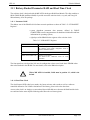
N O T E: The information in this document has been carefully checked and is believed to be entirely reliable. FORCE COMPUTERS makes no warranty of any kind with regard to the material in this document, and assumes no responsibility for any errors that
may appear in this document. FORCE COMPUTERS reserves the right to make changes without notice to this, or any of its products, to improve reliability, performance, or design.
FORCE COMPUTERS assumes no responsibility for the use of any circuitry other than circuitry which is part of a product of
FORCE COMPUTERS Inc./GmbH FORCE COMPUTERS does not convey to the purchaser of the product described herein any
license under the patent rights of FORCE COMPUTERS Inc./GmbH nor the rights of others.
Cirus Logic believes the information contained in this documentation is correct and reliable. However, it is subject to change
without notice. No responsibility is assumed by Cirrus Logic for its use, nor for infringements of patents or other rights of third
parties. This document implies no license under patents or copyrights.
Datasheet AMD AM79C900 Copyright Advanced Micro Devices, Inc. 1992 Reprinted with permission of copyright owner. All
rights reserved
TABLE OF CONTENTS
1 Introduction . . . . . . . . . . . . . . . . . . . . . . . . . . . . . . . . . . . . . . . . . . . . . . . . . . . . . . . .
1.1 Distinguishing Features . . . . . . . . . . . . . . . . . . . . . . . . . . . . . . . . . . . . . . . . .
1.2 General Description . . . . . . . . . . . . . . . . . . . . . . . . . . . . . . . . . . . . . . . . . . . .
1.3 Technical Details. . . . . . . . . . . . . . . . . . . . . . . . . . . . . . . . . . . . . . . . . . . . . . .
1.3.1 CPU . . . . . . . . . . . . . . . . . . . . . . . . . . . . . . . . . . . . . . . . . . . . . . . . .
1.3.2 RAM . . . . . . . . . . . . . . . . . . . . . . . . . . . . . . . . . . . . . . . . . . . . . . . .
1.3.3 Basic Flash EPROM . . . . . . . . . . . . . . . . . . . . . . . . . . . . . . . . . .
1.3.4 User EPROM . . . . . . . . . . . . . . . . . . . . . . . . . . . . . . . . . . . . . . . . .
1.3.5 Ethernet Interface . . . . . . . . . . . . . . . . . . . . . . . . . . . . . . . . . . . . . .
1.3.6 SCSI Interface . . . . . . . . . . . . . . . . . . . . . . . . . . . . . . . . . . . . . . . .
1.3.7 Serial I/O . . . . . . . . . . . . . . . . . . . . . . . . . . . . . . . . . . . . . . . . . . . . .
1.3.8 Parallel I/O . . . . . . . . . . . . . . . . . . . . . . . . . . . . . . . . . . . . . . . . . . .
1.3.9 CIO Counters/ Timers . . . . . . . . . . . . . . . . . . . . . . . . . . . . . . . . . . .
1.3.10 Parameter RAM and Real-Time Clock . . . . . . . . . . . . . . . . . . . . . .
1.3.11 VIC Timer . . . . . . . . . . . . . . . . . . . . . . . . . . . . . . . . . . . . . . . . . . . .
1.3.12 Watchdog Timer . . . . . . . . . . . . . . . . . . . . . . . . . . . . . . . . . . . . . . .
1.3.13 Status Display . . . . . . . . . . . . . . . . . . . . . . . . . . . . . . . . . . . . . . . . .
1.3.14 Reset . . . . . . . . . . . . . . . . . . . . . . . . . . . . . . . . . . . . . . . . . . . . . . . .
1.3.15 VMEbus Interface . . . . . . . . . . . . . . . . . . . . . . . . . . . . . . . . . . . . .
1.3.15.1 System Controller . . . . . . . . . . . . . . . . . . . . . . . . . . . . .
1.3.15.2 VMEbus Master Interface . . . . . . . . . . . . . . . . . . . . . . .
1.3.15.3 VMEbus Slave Interface . . . . . . . . . . . . . . . . . . . . . . . .
1.3.16 Interrupt Sources . . . . . . . . . . . . . . . . . . . . . . . . . . . . . . . . . . . . . .
1.3.17 Software . . . . . . . . . . . . . . . . . . . . . . . . . . . . . . . . . . . . . . . . . . . . .
1.3.17.1 Power-On Initialization . . . . . . . . . . . . . . . . . . . . . . . . .
1.3.17.2 Configuration. . . . . . . . . . . . . . . . . . . . . . . . . . . . . . . . .
1.3.17.3 External Callable I/O Functions . . . . . . . . . . . . . . . . . .
1.3.17.4 Application Hooks. . . . . . . . . . . . . . . . . . . . . . . . . . . . .
1.4 Definition of Board Parameters . . . . . . . . . . . . . . . . . . . . . . . . . . . . . . . . . . .
1.4.1 VMEbus . . . . . . . . . . . . . . . . . . . . . . . . . . . . . . . . . . . . . . . . . . . . .
1.4.2 Ethernet . . . . . . . . . . . . . . . . . . . . . . . . . . . . . . . . . . . . . . . . . . . . .
1.4.3 SCSI . . . . . . . . . . . . . . . . . . . . . . . . . . . . . . . . . . . . . . . . . . . . . . . .
1.4.4 Serial I/O . . . . . . . . . . . . . . . . . . . . . . . . . . . . . . . . . . . . . . . . . . . . .
1.4.5 Parallel I/O . . . . . . . . . . . . . . . . . . . . . . . . . . . . . . . . . . . . . . . . . . .
1.4.6 MTBF Values . . . . . . . . . . . . . . . . . . . . . . . . . . . . . . . . . . . . . . . . .
1.4.7 Environmental Conditions . . . . . . . . . . . . . . . . . . . . . . . . . . . . . . .
1.4.8 Power Requirements . . . . . . . . . . . . . . . . . . . . . . . . . . . . . . . . . . .
1-1
1-1
1-2
1-4
1-4
1-5
1-6
1-6
1-6
1-6
1-7
1-7
1-7
1-7
1-7
1-7
1-8
1-8
1-8
1-8
1-9
1-9
1-9
1-9
1-10
1-10
1-10
1-10
1-10
1-10
1-11
1-12
1-12
1-12
1-12
1-12
1-12
2 Installation . . . . . . . . . . . . . . . . . . . . . . . . . . . . . . . . . . . . . . . . . . . . . . . . . . . . . . . . .
2.1 Introduction. . . . . . . . . . . . . . . . . . . . . . . . . . . . . . . . . . . . . . . . . . . . . . . . . . .
2.1.1 Board Installation . . . . . . . . . . . . . . . . . . . . . . . . . . . . . . . . . . . . .
2.1.2 Serial Interface Level Converter (SILC). . . . . . . . . . . . . . . . . . . . .
2.1.3 Installation Parallel I/O . . . . . . . . . . . . . . . . . . . . . . . . . . . . . . . . . .
2.1.4 Ethernet Installation . . . . . . . . . . . . . . . . . . . . . . . . . . . . . . . . . . . .
2.1.5 Pure 8-bit SCSI Installation . . . . . . . . . . . . . . . . . . . . . . . . . . . . . .
2-1
2-1
2-1
2-1
2-2
2-2
2-2
i
TABLE OF CONTENTS
2.1.6 Pure 16-bit SCSI Installation . . . . . . . . . . . . . . . . . . . . . . . . . . . . .
2.1.7 Mixed 8/16 bit SCSI Installation. . . . . . . . . . . . . . . . . . . . . . . . . . .
2.2 Default Board Setting . . . . . . . . . . . . . . . . . . . . . . . . . . . . . . . . . . . . . . . . . . .
2.3 Jumpers and Switches . . . . . . . . . . . . . . . . . . . . . . . . . . . . . . . . . . . . . . . . . . .
2.3.1 Watchdog Period (J1401) . . . . . . . . . . . . . . . . . . . . . . . . . . . . . . .
2.3.2 Flash EPROM Programming Voltage (J1601) . . . . . . . . . . . . . . . .
2.3.3 Pin 1 Connection of EPROM (J1605). . . . . . . . . . . . . . . . . . . . . . .
2.3.4 Reserved Jumper (J1802) . . . . . . . . . . . . . . . . . . . . . . . . . . . . . . .
2.3.5 Switches . . . . . . . . . . . . . . . . . . . . . . . . . . . . . . . . . . . . . . . . . . . . .
2.3.5.1 VMEbus Slave Address (S901). . . . . . . . . . . . . . . . . . . .
2.3.5.2 Hardware Configuration (S902) . . . . . . . . . . . . . . . . . . .
2.3.5.3 System Controller Switch (S3) . . . . . . . . . . . . . . . . . . . .
2-2
2-2
2-4
2-6
2-6
2-6
2-7
2-7
2-7
2-8
2-8
2-9
3 Hardware User’s Manual. . . . . . . . . . . . . . . . . . . . . . . . . . . . . . . . . . . . . . . . . . . . . .
3.1 Address Map . . . . . . . . . . . . . . . . . . . . . . . . . . . . . . . . . . . . . . . . . . . . . . . . . .
3.2 DRAM. . . . . . . . . . . . . . . . . . . . . . . . . . . . . . . . . . . . . . . . . . . . . . . . . . . . . . .
3.2.1 RAM Access From the Local CPU . . . . . . . . . . . . . . . . . . . . . . . . .
3.2.2 RAM Access from the VMEbus . . . . . . . . . . . . . . . . . . . . . . . . . . .
3.2.3 Address Translation. . . . . . . . . . . . . . . . . . . . . . . . . . . . . . . . . . . . .
3.2.4 RAM Mirror . . . . . . . . . . . . . . . . . . . . . . . . . . . . . . . . . . . . . . . . . .
3.2.5 RAM Access from ILACC . . . . . . . . . . . . . . . . . . . . . . . . . . . . . . .
3.3 VMEbus Interface. . . . . . . . . . . . . . . . . . . . . . . . . . . . . . . . . . . . . . . . . . . . . .
3.3.1 System Controller . . . . . . . . . . . . . . . . . . . . . . . . . . . . . . . . . . . . . .
3.3.2 VMEbus Master Interface . . . . . . . . . . . . . . . . . . . . . . . . . . . . . . . .
3.3.2.1 Longword Access to Wordwide Slaves. . . . . . . . . . . . . .
3.3.2.2 Address Modifier Source. . . . . . . . . . . . . . . . . . . . . . . . .
3.3.2.3 Read-Modify-Write Cycles . . . . . . . . . . . . . . . . . . . . . . .
3.3.2.4 VMEbus Block Transfer Option . . . . . . . . . . . . . . . . . . .
3.3.2.5 A16 Slave Interface (ICMS, ICGS) . . . . . . . . . . . . . . . .
3.4 Ethernet Interface (802.3/10base5). . . . . . . . . . . . . . . . . . . . . . . . . . . . . . . . .
3.5 CIO Counter / Timers . . . . . . . . . . . . . . . . . . . . . . . . . . . . . . . . . . . . . . . . . . .
3.6 Serial I/O. . . . . . . . . . . . . . . . . . . . . . . . . . . . . . . . . . . . . . . . . . . . . . . . . . . .
3.6.1 Serial Port Multi-Protocol Controller (MPC) . . . . . . . . . . . . . . .
3.7 Watchdog Timer . . . . . . . . . . . . . . . . . . . . . . . . . . . . . . . . . . . . . . . . . . . . . .
3.8 IOC-2 . . . . . . . . . . . . . . . . . . . . . . . . . . . . . . . . . . . . . . . . . . . . . . . . . . . . . .
3.8.1 Register Set . . . . . . . . . . . . . . . . . . . . . . . . . . . . . . . . . . . . . . . . .
3.9 SCSI Interface. . . . . . . . . . . . . . . . . . . . . . . . . . . . . . . . . . . . . . . . . . . . . . . .
3.9.1 SCSI Controller . . . . . . . . . . . . . . . . . . . . . . . . . . . . . . . . . . . . . . .
3.10 Front Panel Status Display . . . . . . . . . . . . . . . . . . . . . . . . . . . . . . . . . . . . . .
3.11 Battery-Backed Parameter RAM and Real-Time Clock. . . . . . . . . . . . . . . .
3.11.1 Parameter RAM. . . . . . . . . . . . . . . . . . . . . . . . . . . . . . . . . . . . . . .
3.11.1.1 Real-Time Clock . . . . . . . . . . . . . . . . . . . . . . . . . . . . .
3.12 VIC Timer . . . . . . . . . . . . . . . . . . . . . . . . . . . . . . . . . . . . . . . . . . . . . . . . . . .
3-1
3-1
3-2
3-2
3-3
3-4
3-5
3-5
3-5
3-5
3-6
3-6
3-6
3-6
3-7
3-7
3-8
3-9
3-10
3-10
3-12
3-12
3-12
3-14
3-14
3-14
3-15
3-15
3-15
3-16
ii
TABLE OF CONTENTS
3.13 Reset . . . . . . . . . . . . . . . . . . . . . . . . . . . . . . . . . . . . . . . . . . . . . . . . . . . . . . .
3.14 Bus Time-Out . . . . . . . . . . . . . . . . . . . . . . . . . . . . . . . . . . . . . . . . . . . . . . . .
3.15 System Control Register (SCR) . . . . . . . . . . . . . . . . . . . . . . . . . . . . . . . . . .
3.16 Interrupt Sources. . . . . . . . . . . . . . . . . . . . . . . . . . . . . . . . . . . . . . . . . . . . . .
3.16.1 Local Interrupt Sources . . . . . . . . . . . . . . . . . . . . . . . . . . . . . . . .
3.16.2 VMEbus Interrupt Sources . . . . . . . . . . . . . . . . . . . . . . . . . . . . . .
3.16.3 Cache Coherency and Snooping . . . . . . . . . . . . . . . . . . . . . . . . .
3.17 Revision Information . . . . . . . . . . . . . . . . . . . . . . . . . . . . . . . . . . . . . . . . . .
3.18 Indivisible Cycle Operation . . . . . . . . . . . . . . . . . . . . . . . . . . . . . . . . . . . . .
3.18.1 Deadlock Resolution . . . . . . . . . . . . . . . . . . . . . . . . . . . . . . . . . .
3.18.2 TAS Violation . . . . . . . . . . . . . . . . . . . . . . . . . . . . . . . . . . . . . . . .
3-16
3-17
3-18
3-18
3-20
3-20
3-21
3-21
3-22
3-22
3-23
4 Appendicies to the Hardware User’s Manual . . . . . . . . . . . . . . . . . . . . . . . . . . . . . 4-1
4.1 Mnemonics Chart . . . . . . . . . . . . . . . . . . . . . . . . . . . . . . . . . . . . . . . . . . . . . 4-1
4.2 Addressing Capabilities . . . . . . . . . . . . . . . . . . . . . . . . . . . . . . . . . . . . . . . . 4-1
4.3 Data Transfer Capabilities . . . . . . . . . . . . . . . . . . . . . . . . . . . . . . . . . . . . . . 4-2
4.3.1 Master Data Transfer. . . . . . . . . . . . . . . . . . . . . . . . . . . . . . . . . . . 4-2
4.3.2 Slave Data Transfer . . . . . . . . . . . . . . . . . . . . . . . . . . . . . . . . . . . . 4-3
4.3.3 Location Monitor Data Transfer . . . . . . . . . . . . . . . . . . . . . . . . . 4-3
4.4 Glossary . . . . . . . . . . . . . . . . . . . . . . . . . . . . . . . . . . . . . . . . . . . . . . . . . . . . 4-3
4.5 Address Modifiers on VMEbus . . . . . . . . . . . . . . . . . . . . . . . . . . . . . . . . . . 4-4
4.6 Connectors . . . . . . . . . . . . . . . . . . . . . . . . . . . . . . . . . . . . . . . . . . . . . . . . . . 4-5
4.7 References. . . . . . . . . . . . . . . . . . . . . . . . . . . . . . . . . . . . . . . . . . . . . . . . . . . 4-10
5 Copies of Data Sheets . . . . . . . . . . . . . . . . . . . . . . . . . . . . . . . . . . . . . . . . . . . . . . .
5-1
MC68040 Data Sheet and Errata
CIO Z8536
IOC-2
VIC 68 User’s Guide
VIC 64 Design Notes
NCR 53C720 Data Sheet
53C720 Programmers Guide
CL-CD2400/CD2401
ILACC Am79C900 Data Sheet
FORCE COMPUTERS Product Error Report
6 Firmware User’s Manual . . . . . . . . . . . . . . . . . . . . . . . . . . . . . . . . . . . . . . . . . . . . .
6.1 Distinguishing Features . . . . . . . . . . . . . . . . . . . . . . . . . . . . . . . . . . . . . . . .
6.2 General Description . . . . . . . . . . . . . . . . . . . . . . . . . . . . . . . . . . . . . . . . . . .
6.3 Technical Details. . . . . . . . . . . . . . . . . . . . . . . . . . . . . . . . . . . . . . . . . . . . . .
6.3.1 Hardware Test . . . . . . . . . . . . . . . . . . . . . . . . . . . . . . . . . . . . . . .
6.3.2 Hardware Initialization . . . . . . . . . . . . . . . . . . . . . . . . . . . . . . . .
6.3.3 Network Boot and Bootstrap for OS-9 . . . . . . . . . . . . . . . . . . . .
6.3.4 Interactive Mode . . . . . . . . . . . . . . . . . . . . . . . . . . . . . . . . . . . . . .
6.4 Default Parameters . . . . . . . . . . . . . . . . . . . . . . . . . . . . . . . . . . . . . . . . . . . .
iii
6-1
6-1
6-2
6-4
6-4
6-5
6-5
6-5
6-6
TABLE OF CONTENTS
6.5 Hardware Test . . . . . . . . . . . . . . . . . . . . . . . . . . . . . . . . . . . . . . . . . . . . . . . . .
6.5.1 Status Display . . . . . . . . . . . . . . . . . . . . . . . . . . . . . . . . . . . . . . . . .
6.5.2 RMon EPROM . . . . . . . . . . . . . . . . . . . . . . . . . . . . . . . . . . . . . . . .
6.5.3 System CIO . . . . . . . . . . . . . . . . . . . . . . . . . . . . . . . . . . . . . . . . . .
6.5.4 VIC Access . . . . . . . . . . . . . . . . . . . . . . . . . . . . . . . . . . . . . . . . . . .
6.5.5 Main Memory . . . . . . . . . . . . . . . . . . . . . . . . . . . . . . . . . . . . . . . . .
6.5.6 VMEbus Slave Address Decoder Register . . . . . . . . . . . . . . . . . . .
6.5.7 Timekeeper RAM . . . . . . . . . . . . . . . . . . . . . . . . . . . . . . . . . . . . . .
6-6
6-7
6-7
6-7
6-7
6-7
6-8
6-8
6.6 Hardware Initialization . . . . . . . . . . . . . . . . . . . . . . . . . . . . . . . . . . . . . . . . . . . . . .
6.6.1 Configuration Switches . . . . . . . . . . . . . . . . . . . . . . . . . . . . . . . .
6.6.1.1 System Configuration Values . . . . . . . . . . . . . . . . . . . . . .
6.6.1.2 VIC . . . . . . . . . . . . . . . . . . . . . . . . . . . . . . . . . . . . . . . . . .
6.6.1.3 Slave Address Decoder . . . . . . . . . . . . . . . . . . . . . . . . . .
6.6.1.4 Character I/O . . . . . . . . . . . . . . . . . . . . . . . . . . . . . . . . . .
6.6.1.5 SCSI Controller . . . . . . . . . . . . . . . . . . . . . . . . . . . . . . . .
6.6.1.6 Watchdog . . . . . . . . . . . . . . . . . . . . . . . . . . . . . . . . . . . . .
6.6.1.7 User Initialization. . . . . . . . . . . . . . . . . . . . . . . . . . . . . . .
6.6.2 Starting a User Program Module. . . . . . . . . . . . . . . . . . . . . . . . . . .
6.6.3 Autoboot . . . . . . . . . . . . . . . . . . . . . . . . . . . . . . . . . . . . . . . . . . . . .
6.7 Interactive Mode . . . . . . . . . . . . . . . . . . . . . . . . . . . . . . . . . . . . . . . . . . . . . .
6.7.1 Introduction . . . . . . . . . . . . . . . . . . . . . . . . . . . . . . . . . . . . . . . . . . .
6.7.2 General Operation . . . . . . . . . . . . . . . . . . . . . . . . . . . . . . . . . . . . . .
6.7.2.1 Command Input . . . . . . . . . . . . . . . . . . . . . . . . . . . . . . . .
6.7.2.2 On-line Help. . . . . . . . . . . . . . . . . . . . . . . . . . . . . . . . . . .
6.7.2.3 Special Keys. . . . . . . . . . . . . . . . . . . . . . . . . . . . . . . . . . .
6.7.2.4 Data Input Formats. . . . . . . . . . . . . . . . . . . . . . . . . . . . . .
6.7.3 Formal Syntax Notation . . . . . . . . . . . . . . . . . . . . . . . . . . . . . . . . .
6.7.4 Command Description . . . . . . . . . . . . . . . . . . . . . . . . . . . . . . . . . .
6.7.4.1 Boot . . . . . . . . . . . . . . . . . . . . . . . . . . . . . . . . . . . . . . . .
6.7.4.2 Display Memory. . . . . . . . . . . . . . . . . . . . . . . . . . . . . . .
6.7.4.3 Run Module . . . . . . . . . . . . . . . . . . . . . . . . . . . . . . . . . .
6.7.4.4 Help . . . . . . . . . . . . . . . . . . . . . . . . . . . . . . . . . . . . . . . .
6.7.4.5 Modify Memory . . . . . . . . . . . . . . . . . . . . . . . . . . . . . . .
6.7.4.6 Read Parameters from NVRAM . . . . . . . . . . . . . . . . . .
6.7.4.7 SCSI Bus Scan . . . . . . . . . . . . . . . . . . . . . . . . . . . . . . . .
6.7.4.8 System Setup . . . . . . . . . . . . . . . . . . . . . . . . . . . . . . . . .
6.7.4.9 Load S-Records . . . . . . . . . . . . . . . . . . . . . . . . . . . . . . .
6.7.4.10 Transparent Mode . . . . . . . . . . . . . . . . . . . . . . . . . . . . .
6.7.4.11 Write Parameters to NVRAM . . . . . . . . . . . . . . . . . . . .
6-8
6-8
6-9
6-9
6-9
6-9
6-9
6-10
6-10
6-10
6-10
6-11
6-11
6-11
6-11
6-12
6-12
6-13
6-13
6-14
6-15
6-15
6-15
6-16
6-16
6-17
6-17
6-18
6-18
6-19
6-19
7 RMon Programmers Reference . . . . . . . . . . . . . . . . . . . . . . . . . . . . . . . . . . . . . . . . .
7.1 Programming Interface . . . . . . . . . . . . . . . . . . . . . . . . . . . . . . . . . . . . . . . . . .
7.1.1 Module Header . . . . . . . . . . . . . . . . . . . . . . . . . . . . . . . . . . . . . . . .
7.1.2 User Applicable Routines . . . . . . . . . . . . . . . . . . . . . . . . . . . . . . . .
7-1
7-1
7-1
7-2
iv
TABLE OF CONTENTS
7.1.2.1 Character In . . . . . . . . . . . . . . . . . . . . . . . . . . . . . . . . . .
7.1.2.2 Character Out . . . . . . . . . . . . . . . . . . . . . . . . . . . . . . . .
7.1.2.3 Character I/O Status Read . . . . . . . . . . . . . . . . . . . . . . .
7.1.2.4 Character I/O Mode Set. . . . . . . . . . . . . . . . . . . . . . . . .
7.1.2.5 Getchar . . . . . . . . . . . . . . . . . . . . . . . . . . . . . . . . . . . . .
7.1.2.6 Putchar. . . . . . . . . . . . . . . . . . . . . . . . . . . . . . . . . . . . . .
7.1.2.7 Printf . . . . . . . . . . . . . . . . . . . . . . . . . . . . . . . . . . . . . . .
7.1.2.8 Monitor Re-Entry . . . . . . . . . . . . . . . . . . . . . . . . . . . . .
7.1.2.9 Raw Input . . . . . . . . . . . . . . . . . . . . . . . . . . . . . . . . . . .
7.1.2.10 Raw Output . . . . . . . . . . . . . . . . . . . . . . . . . . . . . . . . .
7.1.2.11 Execute SCSI Command . . . . . . . . . . . . . . . . . . . . . . .
7.2 Internals. . . . . . . . . . . . . . . . . . . . . . . . . . . . . . . . . . . . . . . . . . . . . . . . . . . . .
7.2.1 Memory Map. . . . . . . . . . . . . . . . . . . . . . . . . . . . . . . . . . . . . . . . .
7.2.2 CPU Registers . . . . . . . . . . . . . . . . . . . . . . . . . . . . . . . . . . . . . . . .
7.2.3 Exception Handling . . . . . . . . . . . . . . . . . . . . . . . . . . . . . . . . . . .
7.2.4 Status Indication . . . . . . . . . . . . . . . . . . . . . . . . . . . . . . . . . . . . . .
7.2.5 System Configuration Values . . . . . . . . . . . . . . . . . . . . . . . . . . . .
7.3 ANSI Standard Terminal Emulation . . . . . . . . . . . . . . . . . . . . . . . . . . . . . . .
7.3.1 Control Sequence Syntax . . . . . . . . . . . . . . . . . . . . . . . . . . . . . . .
7.3.2 Supported Control Codes . . . . . . . . . . . . . . . . . . . . . . . . . . . . . . .
7.3.3 Supported ANSI Control Sequences . . . . . . . . . . . . . . . . . . . . . . .
8 Appendices to the Firmware Manual. . . . . . . . . . . . . . . . . . . . . . . . . . . . . . . . . . . .
8.1 Walkthrough Examples . . . . . . . . . . . . . . . . . . . . . . . . . . . . . . . . . . . . . . . . .
8.2 S-Record Format. . . . . . . . . . . . . . . . . . . . . . . . . . . . . . . . . . . . . . . . . . . . . .
8.3 Hardware Self Test . . . . . . . . . . . . . . . . . . . . . . . . . . . . . . . . . . . . . . . . . . . .
8.3.1 Reset . . . . . . . . . . . . . . . . . . . . . . . . . . . . . . . . . . . . . . . . . . . . . . .
8.3.2 System CIO Initialization . . . . . . . . . . . . . . . . . . . . . . . . . . . . . . .
8.3.3 EPROM Checksum . . . . . . . . . . . . . . . . . . . . . . . . . . . . . . . . . . . .
8.3.4 First Access to VIC . . . . . . . . . . . . . . . . . . . . . . . . . . . . . . . . . . . .
8.3.5 Minimum VIC Initialization . . . . . . . . . . . . . . . . . . . . . . . . . . . . .
8.3.6 RAM Test . . . . . . . . . . . . . . . . . . . . . . . . . . . . . . . . . . . . . . . . . . .
8.3.7 VMEbus Address Decoder . . . . . . . . . . . . . . . . . . . . . . . . . . . . . .
8.3.8 Access to Video Controller . . . . . . . . . . . . . . . . . . . . . . . . . . . . . .
8.3.9 Test of CLUT . . . . . . . . . . . . . . . . . . . . . . . . . . . . . . . . . . . . . . . .
8.3.10 Video RAM Test. . . . . . . . . . . . . . . . . . . . . . . . . . . . . . . . . . . . . .
8.3.11 MK48T12/18 BatteIg Test . . . . . . . . . . . . . . . . . . . . . . . . . . . . . .
8.3.12 MK48T12/18 RAM Test . . . . . . . . . . . . . . . . . . . . . . . . . . . . . . .
8.3.13 Secondary CPU . . . . . . . . . . . . . . . . . . . . . . . . . . . . . . . . . . . . . .
8.3.14 Serial Controller Access. . . . . . . . . . . . . . . . . . . . . . . . . . . . . . . .
8.3.15 Serial Controller Register Test . . . . . . . . . . . . . . . . . . . . . . . . . . .
8.3.16 SCSI Controller . . . . . . . . . . . . . . . . . . . . . . . . . . . . . . . . . . . . . .
8.3.17 Watchdog . . . . . . . . . . . . . . . . . . . . . . . . . . . . . . . . . . . . . . . . . . .
8.3.18 Halt and Hang-up . . . . . . . . . . . . . . . . . . . . . . . . . . . . . . . . . . . . .
8.3.19 Exceptions . . . . . . . . . . . . . . . . . . . . . . . . . . . . . . . . . . . . . . . . . .
8.3.20 Untested Peripherals. . . . . . . . . . . . . . . . . . . . . . . . . . . . . . . . . . . .
v
7-3
7-4
7-4
7-4
7-5
7-5
7-6
7-7
7-7
7-8
7-8
7-9
7-9
7-9
7-9
7-10
7-10
7-11
7-11
7-12
7-12
8-1
8-1
8-8
8-9
8-11
8-11
8-11
8-12
8-12
8-12
8-13
8-13
8-13
8-14
8-14
8-14
8-14
8-14
8-14
8-15
8-15
8-15
8-15
8-15
vi
LIST OF TABLES
Table 2.1
Table 2.2
Table 2.3
Table 2.4
Table 2.5
Table 2.6
Table 2.7
Table 2.8
Table 3.1
Table 3.2
Table 3.3
Table 3.4
Table 3.5
Table 3.6
Table 3.7
Table 3.8
Table 3.9
Table 3.10:
Table 3.11
Table 3.12
Table 3.13
Table 3.14
Table 3.15
Table 3.16
Table 3.17
Table 3.18
Table 3.19
Table 3.20
Table 3.21
Table 3.22
Table 4.1
Table 4.2
Table 4.3
Table 4.4
Table 4.5
Default Settings. . . . . . . . . . . . . . . . . . . . . . . . . . . . . . . . . . . . . . . .
J1401 (Watchdog Period) . . . . . . . . . . . . . . . . . . . . . . . . . . . . . . . .
J1601 (Flash EPROM Programming Voltage) . . . . . . . . . . . . . . . .
J1605 (Pin 1 Connection of EPROM) . . . . . . . . . . . . . . . . . . . . . .
J1802 (Reserved) . . . . . . . . . . . . . . . . . . . . . . . . . . . . . . . . . . . . . .
Hex Switch S901 (VMEbus Slave Address) . . . . . . . . . . . . . . . . .
Hex Switch S902 (Hardware Configuration) . . . . . . . . . . . . . . . . .
Switch S3 (System Controller Switch) . . . . . . . . . . . . . . . . . . . . . .
Address Assignment of CPU-44. . . . . . . . . . . . . . . . . . . . . . . . . . .
Local I/O Address Assignment. . . . . . . . . . . . . . . . . . . . . . . . . . . .
SMR and SBR Layout . . . . . . . . . . . . . . . . . . . . . . . . . . . . . . . . . .
Enable Slave Register Layout. . . . . . . . . . . . . . . . . . . . . . . . . . . . .
Intercommunication Register Location on VMEbus . . . . . . . . . . .
ILACC Registers. . . . . . . . . . . . . . . . . . . . . . . . . . . . . . . . . . . . . . .
15-Pin AUI Connector (ETHERNET X801) . . . . . . . . . . . . . . . . .
CIO Counter/Timer Registers . . . . . . . . . . . . . . . . . . . . . . . . . . . .
MPC Baud Rate . . . . . . . . . . . . . . . . . . . . . . . . . . . . . . . . . . . . . .
6-Pin Telephone Jack (Serial RS 232 PORT X1202) . . . . . . . . . .
Watchdog Timer Registers . . . . . . . . . . . . . . . . . . . . . . . . . . . . . .
IOC-2 Register Map . . . . . . . . . . . . . . . . . . . . . . . . . . . . . . . . . . .
NVRAM RTC Registers . . . . . . . . . . . . . . . . . . . . . . . . . . . . . . . .
Real Time Clock Registers . . . . . . . . . . . . . . . . . . . . . . . . . . . . . .
Reset Conditions . . . . . . . . . . . . . . . . . . . . . . . . . . . . . . . . . . . . . .
System Control Register . . . . . . . . . . . . . . . . . . . . . . . . . . . . . . . .
VIC Interrupt Priority Scheme . . . . . . . . . . . . . . . . . . . . . . . . . . .
Local Interrupt Sources. . . . . . . . . . . . . . . . . . . . . . . . . . . . . . . . .
Snoop Control Register Layout . . . . . . . . . . . . . . . . . . . . . . . . . .
Snoop Control Encoding. . . . . . . . . . . . . . . . . . . . . . . . . . . . . . . .
IOC-2 Internal Control Register . . . . . . . . . . . . . . . . . . . . . . . . . .
Extended Revision Information Example (Hexdump) . . . . . . . . .
6-Pin Telephone (Serial RS 232 PORT X1202) . . . . . . . . . . . . . . .
15-Pin AUI Connector (ETHERNET X801) . . . . . . . . . . . . . . . . .
Pin Assignment of VMEbus P1 Connector (X101) . . . . . . . . . . . .
Pin Assignment of P2 Connector X102 . . . . . . . . . . . . . . . . . . . . .
50-Pin I/O Connector X102 (on ADAP-200 and ADAP-220) . . . .
vii
2-4
2-6
2-6
2-7
2-7
2-8
2-8
2-9
3-1
3-2
3-3
3-3
3-8
3-9
3-9
3-10
3-11
3-11
3-12
3-13
3-15
3-16
3-17
3-18
3-19
3-20
3-21
3-21
3-22
3-22
4-5
4-5
4-6
4-7
4-8
Table 4.6
Table 4.7
Table 6.1
Table 6.2
Table 6.3
Table 6.4
Table 6.5
Table 6.6
Table 6.7
Table 6.8
Table 7.1
Table 7.2
Table 7.3
Table 8.1
SCSI Connector 8-bit X103 (on ADAP-200 and ADAP-220) . . . .
SCSI Connector 16-bit X107 (on ADAP-220) . . . . . . . . . . . . . . .
Default RMon Parameters (S1=0, S2=0) . . . . . . . . . . . . . . . . . . . .
Hardware Test Display Values . . . . . . . . . . . . . . . . . . . . . . . . . . . .
System Configuration Values Source . . . . . . . . . . . . . . . . . . . . . . .
Slave Address Selection . . . . . . . . . . . . . . . . . . . . . . . . . . . . . . . . .
RMon Special Keys . . . . . . . . . . . . . . . . . . . . . . . . . . . . . . . . . . .
RMon Input Formats. . . . . . . . . . . . . . . . . . . . . . . . . . . . . . . . . . .
RMon Syntax Description . . . . . . . . . . . . . . . . . . . . . . . . . . . . . .
RMon Commands . . . . . . . . . . . . . . . . . . . . . . . . . . . . . . . . . . . . .
RMon Module Header . . . . . . . . . . . . . . . . . . . . . . . . . . . . . . . . . .
RMon Memory Usage . . . . . . . . . . . . . . . . . . . . . . . . . . . . . . . . . .
RMon Status Display . . . . . . . . . . . . . . . . . . . . . . . . . . . . . . . . . .
Hardware Test Display-Values . . . . . . . . . . . . . . . . . . . . . . . . . . .
viii
4-9
4-10
6-6
6-6
6-8
6-9
6-13
6-13
6-13
6-14
7-2
7-9
7-10
8-10
LIST OF FIGURES
Figure 1.1
Figure 2.1
Figure 2.2
Figure 2.3
Figure 2.4
Figure 6.1
Figure 6.2
Figure 8.1
Figure 8.2
Figure 8.3
Figure 8.4
Figure 8.5
Figure 8.6
Figure 8.7
Figure 8.8
Figure 8.9
Figure 8.10
Figure 8.11
Figure 8.12
Block Diagram. . . . . . . . . . . . . . . . . . . . . . . . . . . . . . . . . . . . . . . . . . 1-2
Installation Diagram . . . . . . . . . . . . . . . . . . . . . . . . . . . . . . . . . . . . . 2-3
Location of Jumper (Circuit Side) . . . . . . . . . . . . . . . . . . . . . . . . . . . 2-4
Location of Jumpers, Interface Connectors and Switches. . . . . . . . . 2-5
Switches S901 to S4 . . . . . . . . . . . . . . . . . . . . . . . . . . . . . . . . . . . . . 2-7
Block Diagram. . . . . . . . . . . . . . . . . . . . . . . . . . . . . . . . . . . . . . . . . . 6-2
RMon Start-up Display . . . . . . . . . . . . . . . . . . . . . . . . . . . . . . . . . . 6-11
Main Menu . . . . . . . . . . . . . . . . . . . . . . . . . . . . . . . . . . . . . . . . . . . . 8-1
VMEbus Interface Menu . . . . . . . . . . . . . . . . . . . . . . . . . . . . . . . . . . 8-2
VMEbus Slave Access Parameters . . . . . . . . . . . . . . . . . . . . . . . . . . 8-2
VMEbus Master Access Parameters . . . . . . . . . . . . . . . . . . . . . . . . . 8-3
VMEbus Arbiter/Requester/Time-out Parameter . . . . . . . . . . . . . . . 8-3
VMEbus Interrupt Parameter. . . . . . . . . . . . . . . . . . . . . . . . . . . . . . . 8-4
Serial Interface Menu . . . . . . . . . . . . . . . . . . . . . . . . . . . . . . . . . . . . 8-4
Serial Port 1 Parameters . . . . . . . . . . . . . . . . . . . . . . . . . . . . . . . . . . 8-5
SCSI/Keyboard Interface Menu . . . . . . . . . . . . . . . . . . . . . . . . . . . . 8-5
Boot Parameters. . . . . . . . . . . . . . . . . . . . . . . . . . . . . . . . . . . . . . . . . 8-6
Hooks. . . . . . . . . . . . . . . . . . . . . . . . . . . . . . . . . . . . . . . . . . . . . . . . . 8-7
Special Menu . . . . . . . . . . . . . . . . . . . . . . . . . . . . . . . . . . . . . . . . . . . 8-8
ix
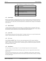
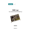
Photograph of the CPU-44
x
xi
LIST OF FIGURES
Figure
Figure
Figure
Figure
Figure
Figure
Figure
Figure
Figure
Figure
Figure
Figure
Figure
Figure
Figure
Figure
Figure
Figure
Figure
1.1 Block Diagram
. . . . . . . . . . . . . . . .
2.1 Installation Diagram
. . . . . . . . . . . . . .
2.2 Location of Jumper (Circuit Side) . . . . . . . . .
2.3 Location of Jumpers, Interface Connectors and Switches
2.4 Switches S901 to S4 . . . . . . . . . . . . . .
6.1 Block Diagram
. . . . . . . . . . . . . . . .
6.2 RMon Start-up Display . . . . . . . . . . . . .
8.1 Main Menu . . . . . . . . . . . . . . . . . .
8.2 VMEbus Interface Menu
. . . . . . . . . . . .
8.3 VMEbus Slave Access Parameters
. . . . . . . .
8.4 VMEbus Master Access Parameters . . . . . . . .
8.5 VMEbus Arbiter/Requester/Time-out Parameter . . .
8.6 VMEbus Interrupt Parameter . . . . . . . . . . .
8.7 Serial Interface Menu . . . . . . . . . . . . . .
8.8 Serial Port 1 Parameters . . . . . . . . . . . . .
8.9 SCSI/Keyboard Interface Menu . . . . . . . . . .
8.10 Boot Parameters . . . . . . . . . . . . . . . .
8.11 Hooks . . . . . . . . . . . . . . . . . . . .
8.12 Special Menu . . . . . . . . . . . . . . . . .
xii
. . .1-2
. . .2-3
. . .2-4
. . .2-5
. . .2-7
. . .6-2
. . 6-11
. . .8-1
. . .8-2
. . .8-2
. . .8-3
. . .8-3
. . .8-4
. . .8-4
. . .8-5
. . .8-5
. . .8-6
. . .8-7
. . .8-8
xiii
CPU-44
Technical Manual
1 Introduction
1.1 Distinguishing Features
• 68040 CPU at 25 MHz or 33 MHz
• Memory
- Up to 32 MB RAM for data/program storage (79 MB/s)
- 8 KB SRAM and RTC for storage of variable system parameters
(MK48T18)
- Up to 1 MB user EPROM
- 256 KB basic Flash EPROM for firmware
• Ethernet interface (32-bit ILACC)
• VMEbus interface controller:
- System controller and arbiter
- VMEbus interrupter and interrupt handler
- Master/slave write posting
- 64-bit MBLT 35 MB/s
• IOC-2 gate array:
- 68040 to 68020 bus converter
- Dynamic bus sizing for VMEbus
- Translation of BLT into bursts on '040 bus to allow snooping of BLT
cycles
- Separate arbitration on '040 and '020 bus
- I/O bus interface
- Support for VMEbus UATs to allow snooping
- Interface for a single bytewide EPROM
• Parallel I/O or Centronics port
• Six 16-bit timer/counters
• Four serial ports (RS 232, RS 422, RS 485)
• Smart SCSI-2 (NCR 53C720) interface with burst capability (max. transfer
capacity 20 MB/s) and single-ended 8/16-bit SCSI data bus
• Two rotary switches on front panel for selection of operation modes and
base address
• Status display on front panel
• Watchdog timer with watchdog indicator on front panel
FORCE COMPUTERS
049-13856-101 Rev A1
Page 1-1
Technical Manual
CPU-44
1.2 General Description
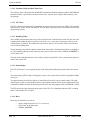
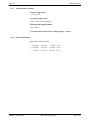
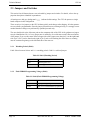
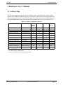
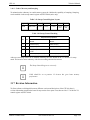
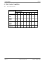
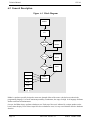
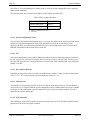
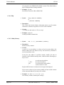
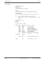
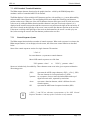
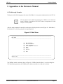
Figure 1.1 Block Diagram
DRAM
max . 32 MB
NCR 53C720
SCSI
Controller
VMEbus
8/16 bit SCSI-2
X101
CPU
68040
33 MHz
‘040 Bus
Front
Panel
I/O Bus
IOC-2
CIO
8536
Display
‘020 Bus
Slave Addr.
Watchdog
Operation
Mode
1M x 8
User EPROM
VIC
VMEbus
Controller
VIC-64
VMEbus
Buffer/Count./
Decoder
Syscon
2K x 8
NVRAM
RTC
CIO
8536
X102
256K x 8
Flash EPROM
Res/Stat.
Row A
Row C
Parallel/Timer
8536
.2 bit Parallel
Centronics
Row B
RS 232
Serial
Controller
3x
RS 232
Serial Line
A
U
I
Ethernet
Controller
ILACC
The CPU-44 is a highly integrated high-performance single-board VMEbus computer with graphics display. It is designed to offer as many features as possible on a single slot VMEbus board. Suitable intelligent or high integrated components are used to achieve this density of computing power.
Page 1-2
049-13856-101 Rev A1
FORCE COMPUTERS
CPU-44
Technical Manual
The on-board 68040 CPU is clocked at 25 or 33MHz. On-chip caches for program and data (4 KB capacity
each) and the on-chip floating-point unit allows 35 MIPS/ 5.6 MFLOPS for the CPU. Additionally, backward compatibility with existing 68000-family software is guaranteed.
The main memory is organized in two banks of interleaved DRAM. Therefore, burst mode transfers allow
70 MB/s on reads. Due to a buffered write mechanism, the transfer rate for writes is even bigger (79 MB/
s). This is useful during cache flushes where the CPU may write large amounts of data.
The major drawback of the 68040 is the deletion of dynamic bus sizing. This requires 68020/30 applications to be modified if they access word devices with longword instructions. The longword accesses have
to be split by software into two word accesses. This slows down the performance. Instead of this, the
IOC-2 hardware generates the needed bus cycles if the addressed device acknowledges a smaller data size
than the CPU requested.
One of the main design goals of the CPU-44 is efficient use of the CPU's high speed bus. Thus, the following design rules are established:
•
Use of intelligent peripheral devices which are able to perform tasks independent from the main CPU
(NCR 53C720, CL-CD2401, ILACC).
•
Independent 68020-like bus for VMEbus, Ethernet with separate arbitration.
•
Minimum interference between CPU bus, ‘020 bus and I/O bus.
•
Decoupling of VMEbus and CPU bus via FIFO for BLT. On traditional designs there could only be one
bus master on the whole board at a time. For example, if a BLT was in progress, the CPU was blocked
for the duration of the BLT. On the CPU-44 the CPU bus is decoupled from the I/O bus.
In order to enhance system security, the CPU-44 incorporates a watchdog timer. It must be retriggered periodically otherwise the watchdog generates a reset. After watchdog reset, the watchdog reset LED on the
front panel signals this condition. The watchdog indicator is cleared only by power-on reset or by triggering the watchdog.
Four serial ports are located on the CPU-44. One, using a 6-pin RJ11 jack on the front panel, is intended
for connection of a terminal or a mouse. The other three are fed to rows A and C of the VMEbus P2 connector (X102). They can be connected via ADAP-220/200 and CONV-300 to three 9-pin D-Sub connectors. Two of the serial lines can be configured to support either RS 232 or RS 422/485 standard via SILCs
(Serial Interface Level Converters).
Twelve parallel I/O-lines (X102) can be used either as centronics printer port or as TTL-level interface
(CONV-300).
The integrated real-time clock allows the operating system to provide date and time for revision control.
The clock is powered by an internal lithium battery. (8)KB of battery-backed RAM is used for storage of
system dependent parameters.
Status displays a reset switch, and two hex-code switches are located on the front panel. The status display
indicates the condition of the processor and watchdog timer. The hexadecimal display is an error status display. The hex-code switches (software readable) are used by the firmware to set up the operating mode and
the VMEbus base address of the board.
The VMEbus interface of the CPU-44 uses the VIC-64 VMEbus Interface Controller gate array. The VIC64 supports D64 multiplexed block transfer according to IEEE 1014 Rev. D.
A 256 K x 8 Flash EPROM holds the firmware. It is on-board reprogrammable to allow reconfiguration.
FORCE COMPUTERS
049-13856-101 Rev A1
Page 1-3
Technical Manual
CPU-44
Up to 1M x 8 of EPROM can be added to the board to hold user firmware.
The onboard Ethernet interface provides connection to most popular local area networks (LAN).
A sophisticated SCSI-2 (wide) interface is also located on the CPU-44. The controller chip is very fast and
intelligent so that it forms a very efficient SCSI interface with a maximum transfer rate of 20 MB/s.
1.3 Technical Details
The CPU-44 consists of the following main blocks:
•
•
•
•
•
•
•
•
•
•
•
•
•
•
•
•
•
•
1.3.1
CPU
RAM
Basic Flash EPROM
User EPROM
Ethernet Interface
SCSI Interface
Serial I/0
Parallel I/O
CIO Counters/Timers
Parameter RAM and Real-Time Clock
VIC Timer
Watchdog Timer
Status Display
Reset
VMEbus Interface
Interrupt Sources
Software
Connectors
CPU
The 68040 CPU is clocked with 25 or 33 MHz. All internal bus operations are synchronous to this clock.
The CPU uses burst mode only to access main memory.
The CPU handles all interrupts generated by the VIC. CPU IACK cycles are always routed to the VIC.
Page 1-4
049-13856-101 Rev A1
FORCE COMPUTERS
CPU-44
Technical Manual
Non-interruptable read-modify-write cycles (TAS commands) are supported between VMEbus and the
CPU. RMC cycles from the VMEbus to the local RAM are only indivisible when they are byte size. CAS2
instructions have limited support As shown in Table 1.1.
Table 1.1 CAS2 Operations on the Various Busses
1.3.2
1st op
2nd op
indivisible
local RAM
local RAM
yes
VMEbus
local RAM
yes
local RAM
VMEbus
no
VMEbus
VMEbus
yes
RAM
The DRAM maybe accessed from the following sources:
•
•
•
•
CPU
SCSI Controller
Ethernet Controller
VMEbus
Burst mode is supported for accesses from:
•
•
•
CPU
SCSI Controller
VMEbus BLT
The base address of the DRAM seen from the CPU is fixed to $0000.0000. To avoid programming the
MMU, the DRAM and VRAM are mirrored as non-cacheable RAM.
The base address for accessing the RAM from the VMEbus, as well as the window size, is programmable.
The on-board firmware uses hex switch S901 to program the VMEbus address decoder and mask registers.
i
When using A24 addressing, to access the CPU-44 RAM the address
translation logic must be programmed to supply local addresses A(24) to
A(26). In this case, the DRAM can be reached from VMEbus (including A32
addressing).
The following table summarizes the usable bandwidth of the RAM including precharge and refresh.
Table 1.2: Usable Bandwidth of the RAM
FORCE COMPUTERS
33 MHz: (MB/s)
25 MHz: (MB/s)
DRAM read
58
50
DRAM write
66
50
049-13856-101 Rev A1
Page 1-5
Technical Manual
CPU-44
RAM Performance- The CPU-44C/16 has only one RAM bank and
i
1.3.3
therefore can’t use interleaving. This reduces memory performance a little.
On reads a 5/2/2/2 burst and on writes a 3/2/2/1 burst is done. Including
precharge delays and refresh, the usable bandwidth is 48 MB/s for reads and
writes.
Basic Flash EPROM
After reset, the basic Flash EPROM is mapped to $0000.0000 so the initial stack pointer and reset vector
can be read. During initialization, it is mapped to its normal address ($FE80.0000) and the DRAM is located at address $0000.0000.
The software in the basic Flash EPROM (RMon) initializes all hardware according to the parameters in the
basic Flash EPROM or the NVRAM ($FEC2.0000).
Reprogramming is possible when the appropriate jumpers are set. This should only be done during a firmware update. Reprogramming the basic Flash EPROM with code other than RMon will cause board initialization failures.
i
The EPROMs are the slowest devices on the ‘040 bus. Reading a cache line
(16 bytes) out of the EPROMs last about 4 us. This is very poor for other bus
participants. Especially the following can happen: the ILACC performs a
DMA of four accesses to the RAM. Between each access there is a EPROM
read. Since this last more than 16 us the VMEbus may get a buserror when it
wants to access the board in that situation. Work-around: The EPROMs
are only intended for configuration and booting of the CPU-44. The
EPROMs should not be used after the boot. If it is necessary to execute
code out of the EPROM it should be copied to the RAM before.
1.3.4
User EPROM
The pin assignment of the 32-pin socket corresponds to the JEDEC standard. The socket is designed for
use with 32-pin EPROMs only. These EPROM types range from 1 Mb up to 8 Mb (27C010 to 27C080).
The EPROM access time is programmable via an IOC-2 register from 4 to 36 wait-states (60 ns to 810 ns
maximum access time).
1.3.5
Ethernet Interface
The Ethernet interface is based on the Integrated Local Area Communications Controller (ILACC AM79C900).
A main feature of the ILACC and its on-chip DMA channel is the flexibility and speed of communication.
The internal Manchester Encoder/Decoder of the ILACC is compatible with the IEEE-802.3 specification.
Page 1-6
049-13856-101 Rev A1
FORCE COMPUTERS
CPU-44
Technical Manual
The CPU-44 is attached to Ethernet (Cheapernet, or 10BaseT) networks via the AUI connector on the front
panel .
1.3.6
SCSI Interface
Single-ended 8/16 bit SCSI-2 signals are fed into rows A and C of the VMEbus P2 connector (X102). An
ADAP-220 is plugged onto the rear side of the backplane to interface to standard 8/16-bit SCSI connectors: a 50-pin flat cable connector, and a 68-pin, high density, half pitch connector (SCSI-2 P cable). The
ADAP-220 is also used to interface between these types of cables, allowing different types of connectors
to be mixed in the system.
The ADAP-200 can be used for 8-bit SCSI devices.
The NCR53C720 SCSI controller uses its own code fetching and SCSI data transfer from the onboard
DRAM. The processor executes SCSI SCRIPTS to control the actions on the SCSI and the CPU bus.
SCRIPTS is a specially designed language for easy SCSI protocol handling. It dramatically reduces the
CPU activities. The SCRIPTS processor starts SCSI I/O operations in approximately 500 ns where traditional intelligent host adapters require 2-8 ms.
1.3.7
Serial I/O
The CPU-44 offers four serial I/O lines, implemented by one CL-CD2401 Multi Protocol Controller.
CHAN.1 and CHAN.2 are RS 232 two-wire handshake interfaces. CHAN.3 and CHAN.4 use removable
Serial Interface Level Converters (SILC). As shipped, two RS 232 level converter SILCs are installed, featuring hardware handshake as well as the XON / XOFF protocol. Additional level converter plug-ins for
RS 422 and RS 485 are available.
The baud rate generator is driven by a 20 MHz clock, allowing baud rates from 50 b/s to 64 kb/s.
1.3.8
Parallel I/O
There is one 8-bit parallel port with handshake signals on the CPU-44. This parallel port is based on a
Zilog Z8536 device (user CIO). The port signals are routed via the VMEbus P2 connector and the
ADAP-220/200 to the CONV-300 board. Three 9-pin D-Sub serial plugs, a 25-pin D-Sub parallel connector (Centronics printer interface), and a 26-pin connector for direct access to the CIO pins are installed on
the CONV-300.
The I/O ports of the user CIO feature programmable polarity, programmable direction (bit mode), pulse
generators, and programmable open drain outputs. Four handshake modes, including 3-wire (like
IEEE-488), are selectable. The CIO is also programmable as a 16-vector interrupt controller.
1.3.9
CIO Counters/ Timers
The CPU-44 offers three independent, programmable 16-bit counters/timers integrated in the user CIO.
They can be used as general-purpose devices with up to four external access lines per counter / timer
(count input, output, gate, and trigger). Port A and port C lines of the user CIO are routed to a 26-pin I/O
connector on the CONV-300 for user applications.
FORCE COMPUTERS
049-13856-101 Rev A1
Page 1-7
Technical Manual
CPU-44
1.3.10 Parameter RAM and Real-Time Clock
The real-time clock is designed with the MK48T18 timekeeper RAM. It combines a 8Kx8 CMOS SRAM
(parameter RAM), a bytewide accessible real-time clock, a crystal, and a long-life lithium battery, all in
one package.
1.3.11 VIC Timer
The VIC contains a timer that can be programmed to output a periodic wave form on LIRQ2. The available
frequencies are 50 Hz, 100 Hz, and 1000 Hz. The VIC timer is typically used as a tick timer for multi-tasking operating systems.
1.3.12 Watchdog Timer
The watchdog timer monitors the activity of the microprocessor. If the microprocessor does not access the
watchdog timer within the time-out period of 100 ms or 1.6 s, a reset pulse is generated. After reset, the
watchdog timer is disabled. The normal time-out period of 100 ms/1.6 s becomes effective after the first
access to the watchdog timer.
The left decimal point of the hex display located at the front panel is illuminated to indicate a watchdog reset. This watchdog indicator is only cleared by power-up reset, the reset switch, a VMEbus SYSRESET, or
a VIC remote reset.
The state of the watchdog indicator can be read by software using bit PA7 of the system control register located in the system CIO.
1.3.13 Status Display
The CPU-44 features a seven-segment display on the front panel and displays hexadecimal values from 0 F.
This status display ($FEC3.0000) is designed as a read / write register and uses the least significant nibble
of the byte.
The right decimal point of the hex display is controlled by PA0 of the system control register. The right
decimal point is used as an initialization status by the monitor program. After reset the right decimal point
is illuminated. RMon switches the decimal point off before the user program in the user EPROM is called.
The LED next to the reset button shows the status of the CPU. It is illuminated when the CPU is running
and it is off when the CPU is halted.
1.3.14 Reset
Reset may be initiated by six sources:
•
•
•
Page 1-8
supply voltage drop below 4.75 V or power-up
reset switch on the front panel
VMEbus SYSRESET
049-13856-101 Rev A1
FORCE COMPUTERS
CPU-44
Technical Manual
•
•
•
VIC remote control reset register
Watchdog
CPU RESET instruction
1.3.15 VMEbus Interface
Each CPU-44 board offers VMEbus master and slave interfaces. Additionally, VMEbus system controller
functions are available via the VMEbus gate array (VIC).
1.3.15.1 System Controller
The CPU-44 features a full slot-one system controller, including SYSCLK, SYSRESET, bus time-out,
IACK daisy chain driver, and a four level arbitration circuit. System controller capabilities are enabled by
setting switch S3 to position 'SC' on the front panel.
1.3.15.2 VMEbus Master Interface
The master interface of the CPU-44 board supports 8, 16, and 32-bit data transfer cycles in A32, A24, and
A16 addressing modes.
A special feature is provided to support longword accesses from the local CPU to D16 VMEbus boards
(dynamic bus sizing). Two control lines of the System Control Register (SCR) enable longword breaking
for the A32 and A24 area.
The VIC chip supplies the VMEbus address modifier signals. This is done by either routing the FC0..2
lines to AM0..2, or by driving these signals by the internal address modifier source register of the VIC
($FEC0.10B7). The AM3..5 lines are driven depending on the actual data size, or by the address modifier
source register. One output signal of the system control register is used to control this option.
The CPU-44 supports master/slave block transfer cycles. Several options within the VIC chip allow the
user to generate different block transfer cycle types.
The overall transfer rate from one CPU-44 to another CPU-44 is approximately 35 MB/s using D64 block
transfer.
1.3.15.3 VMEbus Slave Interface
The CPU-44 supports A32 and A24 slave access to the DRAM and an A16 slave interface to access the interprocessor communication registers. The addresses of all of the slave interfaces are separately programmable.
For full support of the interprocessor features, the CPU-44 has two A16 slave decoders: one for individual
addressing and one for broadcast addressing of the VIC.
FORCE COMPUTERS
049-13856-101 Rev A1
Page 1-9
Technical Manual
CPU-44
1.3.16 Interrupt Sources
Interrupt sources include VMEIRQ local devices and mailbox interrupts. Interrupts can be reprioritized to
any local level using the control registers of the VIC device.
1.3.17 Software
The local CPU-44 firmware (RMon) is stored in the on-board Flash EPROM (FEPROM). RMon provides
the basic software layer of the board. Any operating system or application software is based on the RMon
and uses its functionality:
•
•
•
•
•
Power-On Initialization
Configuration
Various Bootstraps
External Callable I/O Functions
Application Hooks
1.3.17.1 Power-On Initialization
After reset or power-on, the local hardware (VIC, serial I/O, CIO, video, keyboard interface, etc.) must be
initialized by the CPU. The initialization is affected by certain parameters taken either from the on-board
NVRAM or from the Flash EPROM (default values). Hex switch S902 on the front panel selects whether
the NVRAM or the default values are to be used.
The NVRAM parameters are certified by a checksum. If the checksum test fails, the default parameters are
used independent of the switch setting.
After reset or power-on, an automatic selftest routine checks the functionality of the board and displays the
results.
1.3.17.2 Configuration
The configuration program is completely menu driven. The program interactively shows the configuration
parameters and allows their modification:
•
•
•
•
I/O Configuration, e.g.: serial I/O, baud rate, etc.
Bootstrap configuration
Internet address of ILACC
VMEbus Interface Configuration (VIC Programming)
1.3.17.3 External Callable I/O Functions
These Functions include:
•
•
•
•
•
Page 1-10
Enable/Disable IRQs
Get device status
Set device mode
Character raw I/O
C-like functions such as getchar, putchar, printf
049-13856-101 Rev A1
FORCE COMPUTERS
CPU-44
Technical Manual
1.3.17.4 Application Hooks
Application programs may freely use the external callable I/O functions and other information provided in
the ‘RMon Fixed Public Location.’
Furthermore, a ROMed application can very easily be started interactively or automatically after reset or
power-on from RMon. The application autostart mechanism can be installed simply by setting the bootstrap configuration parameters.
1.4 Definition of Board Parameters
1.4.1
VMEbus
• VMEbus interface according to specification ANSI/IEEE
STD 1014-1987 (Rev. D1.4)
• VMEbus Master Capabilities
- MD64
- MRMW8
- MBLT
• VMEbus Slave Capabilities:
- SADO32
- SRMW32
- UAT
- MBLT
• Arbiter Options
- PRI, RRS
- BTO 4 µs to 480 µs
- SYSCLOCK generation
- BBSY filter
• Requester Options
- Any one of BR(0), BR(1), BR(2) or BR(3)
- Programmable release when done
(RWD)
- Release-on-request
(ROR)
- Release-on-bus-clear
(ROC)
- Bus capture and hold
(BCAP)
- Programmable fair request timer 2 µs ... 30 µs.
• Interrupt Handler and Generator Capabilities
- Interrupt handler and generator on IRQ1 to IRQ7.
FORCE COMPUTERS
049-13856-101 Rev A1
Page 1-11
Technical Manual
CPU-44
• Interrupter Options
- Any one of I(n) where 1 ≤ n ≤ 7.
• Address Range
- Programmable extended/standard/short I/O
extended access (A31-A24 and mask)
standard access (A23-A16 and mask)
short I/O (A15 -A8)
- Default: extended access 64 MB, short I/O 256 B
1.4.2
Ethernet
• AUI interface according to 802.3
1.4.3
SCSI
• SCSI-2 wide (8/16 bit single ended)
• Transfer Speed
- asynchronous transfer 5 MB/s (8-bit) 10 MB/s (16-bit)
- synchronous transfer 10 MB/s (8-bit) 20 MB/s (16-bit)
1.4.4
Serial I/O
• 4 channels (50 b/s - 64 kb/s)
• Keyboard:
- MF2/AT mode
1.4.5
Parallel I/O
• 12-bit unbuffered TTL
• CONV-300:
- 12-bit buffered TTL
- Centronics unidirectional
1.4.6
MTBF Values
• 6857 h (computed from MTL HDBK-217E)
• 91883.8 h (realistic value from industry standard experience)
Page 1-12
049-13856-101 Rev A1
FORCE COMPUTERS
CPU-44
1.4.7
Technical Manual
Environmental Conditions
• Storage Temperature:
-35°C to +85°C
• Operating Temperature:
0°C to +50°C (non condensing)
• Maximum Operating Humidity:
85% relative
• Air temperature with forced air cooling of approx. 1 m/sec.
1.4.8
Power Requirements
Approximate, with all options:
FORCE COMPUTERS
+5 VDC
±5 %
- 7.0 A max.
5.0 A typ.
- 0.2 A max.
0.1 A typ.
+12 VDC ±10 %
- 0.2 A max.
0.1 A typ.
-12 VDC ±10 %
049-13856-101 Rev A1
Page 1-13
Technical Manual
Page 1-14
CPU-44
049-13856-101 Rev A1
FORCE COMPUTERS
CPU-44
Technical Manual
2 Installation
2.1 Introduction
•
Carefully remove the board from the shipping carton. Save the original shipping container and
packing material for storing or reshipping the board.
Avoid touching integrated circuits except in an electrostatic free
environment. Electrostatic discharge can damage circuits or shorten
their lifetime.
•
Inspect the board for any shipping damage. If undamaged, the module can be prepared for
system installation.
When unplugging boards from the rack or otherwise handling boards,
do always observe precautions for handling electrostatic devices.
2.1.1
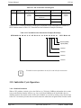
Board Installation
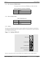
The installation of the CPU-44 is not complicated, requiring only a terminal, a power supply, and a suitable
terminated VMEbus backplane. The power supply must meet the specifications described in Section 1.4
‘Definition of Board Parameters’. The processor board requires a +5 V supply voltage; ±12 V are needed
for the RS 232 serial interface and the Ethernet interface.
2.1.2
Serial Interface Level Converter (SILC)
The Serial Interface Level Converter (SILC) modules generally convert TTL-level signals generated or accepted by the SCC-2 to the appropriate signal levels for external transmission lines. SILC modules for
RS 232C, RS 422 and RS 485 are available.
The mechanical outline of the SILC modules allows the changeability of the different SILC modules on
the CPU-44:
•
SILC-200 for RS 232
•
SILC-300 for RS 422
•
SILC-400 for RS 485
The mechanical part of the installation is very easy. First switch off the VMEbus system and pull the board
out of the rack. If a SILC module is already placed in the connector, remove it carefully. Now plug the new
SILC module into the corresponding connector on the CPU or I/O board. Consider the polarization of the
SILC module; to avoid damage, check that the pin 1 marked on the back of the SILC corresponds to pin 1
marked on the board.
FORCE COMPUTERS
049-13856-101 Rev A1
Page 2-1
Technical Manual
2.1.3
CPU-44
Installation Parallel I/O
An 8-bit parallel port with handshake signals is available on the CPU-44. The port signals are connected
via connector X102 and the ADAP-200/220 to the CONV-300 board. The three 9-pin Sub-D serial plugs, a
25-pin Sub-D parallel connector to support Centronics printer interface, and a 26-pin connector for direct
access to the CIO pins for user applications are installed on the CONV-300.
The printer port has to be enabled by jumper J1 on the CONV-300 board. A general 25-pin Sub-D to Centronics printer port cable is used to connect a parallel printer to the CPU-44. The printer port supports the
following buffered hardware lines: D(1:8), /STROBE, /ACK, BUSY, and PE.
For user-defined usage of the CIO parallel ports, the printer port has to be disabled with jumper J1 located
on the CONV-300. After that, the 26-pin parallel I/O port supports two CIO parallel ports. For more information about the CIO, refer to the Z8536 data sheet and the CONV-300 Hardware Manual.
2.1.4
Ethernet Installation
A standard Ethernet/Cheapernet MAU can be connected via AUI cable to the 15-pin AUI connector on the
front panel of the CPU-44. The length of the AUI cable is limited to 50 m.
2.1.5
Pure 8-bit SCSI Installation
A 8-bit SCSI bus can be connected to X103 of ADAP-200/220. If the CPU-44 is located at either end of
the SCSI bus, RN601-604 must be installed for signal termination, otherwise RN601-604 must be removed.
2.1.6
Pure 16-bit SCSI Installation
A 16-bit SCSI bus can be connected to X107 of ADAP-220. If the CPU-44 is located at either end of the
SCSI bus, RN601-604 must be installed for signal termination, otherwise RN601-604 must be removed.
2.1.7
Mixed 8/16 bit SCSI Installation
ADAP-220 can be used to build mixed 8/16 bit SCSI bus systems. In this case X103 and X107 are used.
RN601-604 must be removed from the CPU-44 and two of the resistor networks must be plugged into
RN101-102 sockets of the ADAP-220 (note pin 1 marking of the networks and the sockets).
Page 2-2
049-13856-101 Rev A1
FORCE COMPUTERS
CPU-44
Technical Manual
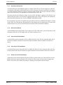
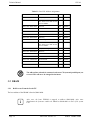
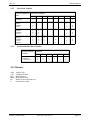
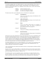
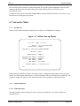
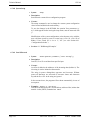
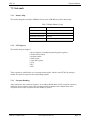
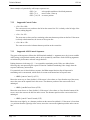
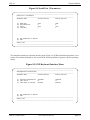
Figure 2.1 Installation Diagram
CPU-44
CONV
Centronics Port
Status Display
SCSI Port
Slave Address
Operating Mode
System Controller
Reset / Status
Parallel I/O (TTL)
Serial (RS 232) Port
RS 232 Port
Ethernet
RS 232 Ports (RS 422, RS 485)
ADAP-200/220
FORCE
FORCE COMPUTERS
049-13856-101 Rev A1
Page 2-3
Technical Manual
CPU-44
2.2 Default Board Setting
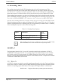
Table 2.1 Default Settings
Jumpers/Switches
Position
Description
J1401
closed
J1601
open
No programming voltage for Flash EPROM,
see Section 2.3.2 ‘Flash EPROM Programming
Voltage (J1601)’
J1605
1-2
See Section 2.3.3 ‘Pin 1 Connection of EPROM
(J1605)’
J1802
1-2
Reserved
S901
0
VMEbus slave address at $8000.0000, see
Section 2.3.5.1 ‘VMEbus Slave Address (S901)’
S902
0
Default initialization values, see Section 2.3.5.2
‘Hardware Configuration (S902)’
SC
System controller enabled, see Section 2.3.5.3
‘System Controller Switch (S3)’
S3
Watchdog period 100 ms,
‘Watchdog Period (J1401)’
see
Section 2.3.1
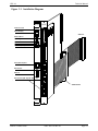
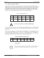
Figure 2.2 Location of Jumper (Circuit Side)
Page 2-4
049-13856-101 Rev A1
FORCE COMPUTERS
CPU-44
Technical Manual
Figure 2.3 Location of Jumpers, Interface Connectors and Switches
FORCE COMPUTERS
049-13856-101 Rev A1
Page 2-5
Technical Manual
CPU-44
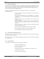
2.3 Jumpers and Switches
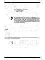
This section lists all features that are user-selectable by jumpers and switches. For details, refer to the appropriate descriptions identified in parentheses.
All settings on a dark grey background (
board computer in this configuration.
) indicate default settings. The CPU-44 operates as single
There are only a few jumpers on the CPU-44 that typically need changes after shipping. All other parameters are software programmable. Since the jumper connections are not changed easily, it is strongly recommended that these changes are performed by qualified personal only.
The user should refer to the silkscreen print on the component side of the CPU-44 for guidance on jumper
area pin identification. Pin 1 of every jumper area is marked by a beveled corner on the silkscreen outline
of the jumper. If you see this corner at the left upper side of the jumper area, then pin 2 is on the right-hand
side of pin 1. Pin 3 can be found on the right of pin 2, and so on. Reaching the end of the row, counting
must be continued beginning on the left-hand side of the next row.
2.3.1
Watchdog Period (J1401)
J1401 Selects between 100 ms and 1.6 s watchdog periods. J1401 is a soldered jumper.
Table 2.2 J1401 (Watchdog Period)
2.3.2
Jumper J1401
Function
open
Watchdog period 1.6 s
closed
Watchdog period 100 ms
Flash EPROM Programming Voltage (J1601)
Table 2.3 J1601 (Flash EPROM Programming Voltage)
Page 2-6
Jumper J1601
Function
open
No programming voltage on Flash EPROM
closed
Apply +12 V to Flash EPROM for programming
049-13856-101 Rev A1
FORCE COMPUTERS
CPU-44
2.3.3
Technical Manual
Pin 1 Connection of EPROM (J1605)
This jumper allows to select between EPROMs up to 4 Mbit and 8 Mbit.
Table 2.4 J1605 (Pin 1 Connection of EPROM)
Jumper J1605
2.3.4
Function
1-2
Pin 1 connected to +5 V (< 8 Mbit)
2-3
Pin 1 connected to A19 (8 Mbit)
Reserved Jumper (J1802)
Table 2.5 J1802 (Reserved)
Jumper J1802
2.3.5
Function
1-2
Default
2-3
Prohibited
Switches
Two rotary hex switches (S901 and S902), the system controller switch (S3) and the reset switch (S4) are
all located on the front panel. If the system controller switch (S3) is switched to the 'SC' position, the board
acts as VMEbus system controller.
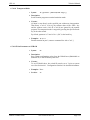
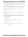
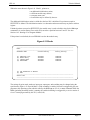
Figure 2.4 Switches S901 to S4
Status Display
Hex Switch (S901)
Hex Switch (S902)
System Controller Switch (S3)
Reset Switch (S4)
Both hex switches (S901, S902) are used by RMon for the configuration setup (see RMon manual).
FORCE COMPUTERS
049-13856-101 Rev A1
Page 2-7
Technical Manual
CPU-44
2.3.5.1 VMEbus Slave Address (S901)
The upper hex switch (S901) selects the CPU-44 slave window address. The size of the A32 slave window
is normally 64 MB. This can be changed by the RMon setup menu. The size of the A16 slave window
(used for VIC access) is 256 bytes.
Table 2.6 Hex Switch S901 (VMEbus Slave Address)
Hex Switch
S901
VMEbus Base Address
A32
A24
A16
F
$F000.0000
disabled
$F000
E
$E000.0000
disabled
$E000
D
$D000.0000
disabled
$D000
.
.
.
.
1
$1000.0000
disabled
$1000
0
Use configuration value
A24 access must be enabled separately.
For a detailed description, see Section 3.2.3 ‘Address Translation’.
i
2.3.5.2 Hardware Configuration (S902)
The lower switch (S902) defines the configuration source and the operation mode. For switch position 0 to
2, RMon enters an interactive mode. If switch S902 is in position 8 to F, the program located in the user
EPROM is called.
Table 2.7 Hex Switch S902 (Hardware Configuration)
Hex Switch
S902
i
Page 2-8
Function
0
Hardware configuration from basic EPROM
1
Hardware configuration from SRAM
2
Hardware configuration from DRAM
3-7
Reserved for FORCE COMPUTER
8-F
Hardware configuration from SRAM and start program in user EPROM.
S901and S902 have no immediate effect. A changed position only becomes
effective after the next reset (i.e. the software reads the switches and
programs the appropriate registers).
049-13856-101 Rev A1
FORCE COMPUTERS
CPU-44
Technical Manual
2.3.5.3 System Controller Switch (S3)
Table 2.8 Switch S3 (System Controller Switch)
Hex Switch S3
left
right 'SC'
FORCE COMPUTERS
Function
System controller disabled
System controller enabled
049-13856-101 Rev A1
Page 2-9
Technical Manual
Page 2-10
CPU-44
049-13856-101 Rev A1
FORCE COMPUTERS
CPU-44
Technical Manual
3 Hardware User’s Manual
3.1 Address Map
The CPU-44 is designed to utilize the entire 4 GB address range of the 68040 chip. Using the address
modifier of the VMEbus, the address range may be enlarged by subdivision into data and program areas
and/or user and supervisor areas. The CPU-44 recognizes two address areas: the local address space and
the global VMEbus address space. The following tables summarize the address space of the CPU-44.
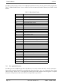
Table 3.1 Address Assignment of CPU-44
VMEbus
Address
Modifier
Cachea
Burstb
local
Y
Y
32
-
-
-
-
local
N
Y
32
-
-
-
-
VMEbus Extended I/O
A32
Nc
N
32/16/8
$FE80.0000 - $FE9F.FFFF
Flash EPROM
local
Y
N
8
$FEA0.0000 - $FEBF.FFFF
User EPROM
local
Y
N
8
$FEC0.0000 - $FECF.FFFF
Local I/O
local
N
N
32/16/8
$FED0.0000 - $FEFF.FFFF
Reserved
-
-
-
-
$FF00.0000 - $FFFE.FFFF
VMEbus Standard I/O
A24
N
N
32/16/8
$FFFF.0000 - $FFFF.FFFF
VMEbus Short I/O
A16
N
N
16/8
Address Range
Device
$0000.0000 - $01FF. FFFF
Local RAM
$0200.0000 - $03FF.FFFF
Reserved
$0400.0000 - $05FF.FFFF
Local RAM (mirrored)
$0610.0000 - $07FF.FFFF
Reserved
$0800.0000 - $FE3F.FFFF
Access
Width [b]
a. Y = /TCI driven high, N = /TCI driven low.
b. Y = /TBI driven high, N = /TBI driven low.
c. Caching may be enabled via System Control Register (SCR).
FORCE COMPUTERS
049-13856-101 Rev A1
Page 3-1
Technical Manual
CPU-44
Table 3.2 Local I/O Address Assignment
Address
Device
Size
Access
$FEC0.0000 - $FEC0.7FFF
VIC (D0..7)
byte
read/write
$FEC0.8000 - $FEC0.FFFF
VMEbus Decoder (D0..31)
see Section 3.2.2 ‘RAM Access
from the VMEbus’
lword
write
$FEC1.0000 - $FEC1.FFFF
User CIO
byte
read/write
$FEC2.0000 - $FEC2.FFFF
NVRAM/RTC
byte
read/write
$FEC3.0000 - $FEC3.FFFF
System CIO
byte
read/write
$FEC4.0000 - $FEC4.FFFF
Reserved
$FEC5.0000 - $FEC5.3FFF
Watchdog
byte
read/write
$FEC5.4000 - $FEC5.7FFF
Revision Register Extension
byte
read
$FEC5.C000 - $FEC5.DFFF
Enable slave select (ESR)
see Section 3.2.2 ‘RAM Access
from the VMEbus’
byte
write
$FEC5.E000 - $FEC5.FFFF
Snoop Control Register
byte
write
$FEC6.0000 - $FEC6.FFFF
Reserved
$FEC6.4000 - $FEC6.7FFF
Serial I/O
byte
read/write
$FEC6.8000 - $FEC6.BFFF
ILACC
lword
read/write
$FEC6.C000 - $FEC6.FFFF
SCSI Controller
lword
read/write
$FEC7.0000 - $FEC7.FFFF
IOC-2
lword
read/write
$FEC8.0000 - $FECF.FFFF
Reserved
-
-
The address lines A0 and A1 connected to the user CIO (external parallel port) are
reversed. This will never be changed in the future.
3.2 DRAM
3.2.1
RAM Access From the Local CPU
The base address of the DRAM is fixed to $0000.0000.
i
Page 3-2
After reset, the basic EPROM is mapped to address $0000.0000. After some
initialization the firmware enables the DRAM at $0000.0000 via PA5 of the system
CIO.
049-13856-101 Rev A1
FORCE COMPUTERS
CPU-44
3.2.2
Technical Manual
RAM Access from the VMEbus
The base address and window size for VMEbus access are specified by the slave base address register
(SBR), the slave mask register (SMR), and the enable slave select register (ESR) of the CPU-44. The SBR
and the SMR are only accessible by the local CPU by longword write cycles. They are undefined after
reset and must be written before the CPU-44 can be accessed from the VMEbus. The ESR is cleared
(disabling all slave accesses) by power-on reset and the reset switch. The ESR can only be accessed by
byte write cycles. The following table describes the contents of the SMR and SBR:
Table 3.3 SMR and SBR Layout
Reg.
Address
31
SMR
$FEC0.80F0
A32 Mask
A24 Mask
ICF1 Mask
ICF2
Decoder
SBR
$FEC0.80F4
A32
Decoder
ext. access
A24
Decoder
std. access
ICF1
Decoder
short I/O
ICF2
Decoder
short I/O
!
24
23
16
15
8
7
0
Do not use other addresses for the SMR and SBR registers.
The A32 decoder compares A31 to A24 of the VMEbus with the SBR bits 32 to 24 for VMEbus extended
access. The A24 decoder compares A23 to A16 of the VMEbus with the SBR bits 23 to 16 for VMEbus
standard access.
The ICF1 decoder compares A15 to A8 of the VMEbus with the SBR bits 15 to 8. If a SMR mask bit is set,
then the corresponding VMEbus address bit is ‘don’t care.’ For full support of the VIC’s interprocessor
communication features, the CPU-44 has a second A16 decoder called the ICF2 decoder. The ESR register
allows separate enabling of the four comparators as shown in the following table:
Table 3.4 Enable Slave Register Layout
Reg.
Address
ESR
$FEC5.C000
7
...
4
unused
3
2
1
0
ICF2
(A16)
ICF1
(A16)
VSTD
(A24)
VEXT
(A32)
1 = Decoder enabled
0 = Decoder disabled
i
FORCE COMPUTERS
Writing the SBR clears all mask bits of the SMR, so that the SBR must be
written before the SMR. Writing the SMR also writes the IFC2 decoder.
049-13856-101 Rev A1
Page 3-3
Technical Manual
3.2.3
CPU-44
Address Translation
The address presented by the VMEbus or the ILACC is translated from the '020 bus (A020) to the '040 bus
(A040) with the help of the MBAR (memory base address register) and ASR (address substitution register)
of the IOC-2. The address on the '040 bus is calculated using the following formula:
A040 = (MBAR & ASR) + (A020 & /ASR)
'&' logical AND operation,
'+' logical OR operation,
'/' logical complement.
The translation is necessary for snooping of the CPU to keep its caches consistent with the memory.
The translated address must always be in the DRAM. If not, the
computer crashes in most cases. Accessing mirrored DRAM locations
has to be avoided because this causes inconsistencies between the
memory and the caches of the CPU. For all address lines not driven by
the source the corresponding bit position in the ASR must be 1 so that
the invalid bits are substituted.
Unfortunately the address translation exists only once for the two address sources (VMEbus, ILACC).
This leads to some restrictions when the DRAM is accessed by A24 addressing from the VMEbus. In this
case only parts of the DRAM can be reached by VMEbus A32 addressing or the ILACC.
Example:
1 MB slave window size for VMEbus A24 addressing at $C0.0000 to the first MB of the DRAM:
MBAR
ASR
SBR
SMR
= $0000.0000
= $FFF0.0000
= $xxC0.xxxx
= $xx0F.xxxx
In this case, VMEbus A32 addressing or the ILACC reach only the local address range $0000.0000 to
$000F.FFFF, (i.e. the first MB of the DRAM).
i
Page 3-4
To avoid problems, FORCE COMPUTERS recommends that VMEbus A24
slave access only be used when absolutely necessary and with extreme care.
If the local RAM/VRAM should be accessed by A24 addressing by the
VMEbus, the MBAR and ASR registers of the IOC-2 must be programmed to
deliver A24-A26 to the local bus. Doing so has impact on VME A32
addressing and RAM access of the ILACC.
049-13856-101 Rev A1
FORCE COMPUTERS
CPU-44
3.2.4
Technical Manual
RAM Mirror
When the CPU uses copyback or writethrough cache mode for the DRAM and snooping is disabled, the
DRAM can become inconsistent with the cache of the CPU. This can cause problems when the data is
accessed by another device (VMEbus, ILACC).
To avoid this problem the CPU can use the cache inhibited RAM mirror ($0400.0000 - $060F.FFFF) for
global data. The other devices must also use the mirrored RAM to avoid accessing data cached in the CPU.
3.2.5
RAM Access from ILACC
The AM79C900 Ethernet Controller uses DMA transfer cycles to transfer commands, data and status
information to and from the DRAM.
3.3 VMEbus Interface
Each CPU-44 board has a VMEbus master and a VMEbus slave interface. Additionally, VMEbus system
controller functions are available via the VMEbus gate array (VIC) used on the CPU-44 board.
3.3.1
System Controller
The CPU-44 features a full slot-one system controller, including SYSCLK, SYSRESET, bus time-out,
IACK daisy chain driver, and a four level arbitration circuit. System controller capabilities are enabled by
moving switch S3 to the 'SC' position on the front panel.
SYSCLK
The SYSCLK is always driven if the system controller
is enabled.
SYSRESET
A low level on this signal resets the internal logic and
asserts the local reset for a minimum of 200 ms. If the
VIC is configured as system controller, the reset switch
on the front panel (S3) asserts the SYSRESET for a
minimum of 200 ms.
Writing a $F0 to the system reset register of the VIC at
address $FEC0.10E3 resets all registers of the VIC and
asserts the SYSRESET output for a minimum of
200 ms.
BTO
FORCE COMPUTERS
The VIC includes two independent bus time-out
modules (BTO) for local cycles and for VMEbus
cycles. The VMEbus time-out is only enabled when
the VIC is configured as system controller. On VIC
reset, the VMEbus time-out period is set to 64 µs and
the local bus time-out period to 32 µs. This can be
altered by programming the transfer time-out register
of the VIC at address $FEC0.10A3. Use the RMon
setup menu to change this value.
049-13856-101 Rev A1
Page 3-5
Technical Manual
CPU-44
Four Level Arbiter If the VIC is configured as system controller, the four
level arbiter is enabled and programmed by writing
into the arbiter/requester configuration register at
address $FEC0.10B3. Use the RMon setup menu to
change this value.
3.3.2
VMEbus Master Interface
The master interface of the CPU-44 board supports 8, 16, and 32-bit data transfer cycles in A32, A24, and
A16 addressing modes. For a short overview, see Section 1.4 ‘Definition of Board Parameters’.
3.3.2.1 Longword Access to Wordwide Slaves
Two different control lines of the system CIO enable longword breaking for the A32 and A24/A16 area:
PA3:
*
0 : forces A24(A16)/D16 data size on VMEbus
1 : allows A24(A16)/D32 data size on VMEbus
PA4:
*
0 : allows A32/D32 data size on VMEbus
1 : forces A32/D16 data size on VMEbus
*
specifies the default values set by RMon.
Use the RMon setup menu for changes.
3.3.2.2 Address Modifier Source
The VIC chip supplies the VMEbus address modifier signals. This is done by either routing FC0..2 lines to
AM0..2, or by driving these signals by an internal address modifier source register of the VIC
($FEC0.10B7). The AM3..5 lines are driven depending on the actual data size, or by the address modifier
source register. One CIO output signal is used to control this option:
PA2:
*
0 : uses CPU and address size dependent modifiers
1 : uses VIC’s address modifier source register
*
specifies the default values set by RMon.
Use the RMon setup menu for changes.
For a detailed description of the address modifier values, see Section 4.5 ‘Address Modifiers on VMEbus’.
3.3.2.3 Read-Modify-Write Cycles
Read-modify-write cycles like TAS or CAS2 are supported by the CPU-44 board.
!
Page 3-6
The CAS2 instruction has only limited support (see Table 1.1 ‘CAS2
Operations on the Various Busses’). The easiest way to ensure that CAS2
instructions are indivisible is to have both operands of the CAS2
instruction within the same memory area (local RAM, VMEbus).
049-13856-101 Rev A1
FORCE COMPUTERS
CPU-44
Technical Manual
3.3.2.4 VMEbus Block Transfer Option
The CPU-44 board supports master/slave block transfer cycles. This is done by the MOVEM.L operation of
the CPU, or by the local DMA device in the VIC. The data size is restricted to D32 and may cross 256 byte
boundaries if the slave is also capable of boundary crossing.
Several options within the VIC chip allow it to generate different block transfer cycle types. The following
code initializes a DMA write block transfer of two times 256 bytes (write block):
MOVE.L
#$4000,d0
local source address
MOVE.L
#$80002000,A1
VMEbus target address
MOVE.B
#$20,$FEC010D3
32 byte blocks
MOVE.B
#$01,$FEC010DB
256 byte total
* disable interrupts which may use VIC or VMEbus
MOVE.B
#$00,$FEC010BF
clear DMA status
MOVE.B
#$40,$FEC010D7
enables DMA block transfer
mode
MOVE.L
D0,(A0)
start DMA block transfer
NOP
LOOP1
BTST
#0,$FEC010BF
wait for BLT finished
BNE
LOOP1
MOVE.B
#$00,$FEC010BF
clear DMA status
ADD.L
#$100,D0
next block
ADD.L
#$100,A0
MOVE.L
D0,(A0)
start DMA block transfer
NOP
LOOP2
BTST
#0,$FEC010BF
wait for BLT finished
BNE
LOOP2
MOVE.B
#$00,$FEC010D7
terminate block transfer
* Interrupts may be enabled
...
During transfer, the user has to check the DMA status register ($FEC0.01BF) and the bus error register of
the VIC ($FEC0.10BB) to see if a VMEbus error condition has occurred. To speed up block transfer
cycles, set bit 1 of the interface configuration register of the VIC ($FEC0.10AF). This may violate the
VMEbus specification, but is guaranteed to operate with any CPU-44 board.
i
i
Block transfer with byte or word size is impossible. Also, the start address
and the transfer length must be multiples of 16 bytes.
If the VIC is programmed to transfer exactly 256 bytes starting at a 256 byte
boundary, the VIC will set the boundary crossing flags in the DMA status
register ($B3). If an interrupt acknowledge occurs between a BLT initiation
cycle and the first transfer, the BLT will malfunction. Work-around: Disable
all interrupts during BLT.
3.3.2.5 A16 Slave Interface (ICMS, ICGS)
A very useful feature of the VIC is a set of registers and switches for message passing or event signaling.
There are eight bytewide general-purpose interprocessor communication registers accessible from the
VMEbus or the local bus (CPU).
• Registers 0 to 4 are general-purpose dual-port registers.
FORCE COMPUTERS
049-13856-101 Rev A1
Page 3-7
Technical Manual
CPU-44
• Register 5 is a dual-port read-only ID register to identify the VIC and its
revision level.
• Register 6 is a module status register that is read-only from the VMEbus.
• Register 7 provides semaphores for registers 0-4 and several system control
functions like a remote reset function.
Four ‘Interprocessor Communication Module Switches’ (ICMS) and four ‘Interprocessor Communication
Global Switches’ (ICGS) are provided by the VIC. These are bytewide mailbox switches to signal events
by generating an interrupt to the local CPU if accessed from the VMEbus. To signal dedicated events/
messages the ICMS locate a unique set of addresses. To support this feature, two separate ICF address
decoders are installed on the CPU-44 board. The ICF1 decoder for dedicated board specific messages and
the ICF2 decoder to feature global messages. Each decoder is enabled separately.
The intercommunication registers within the VIC chip are accessible in A16 VMEbus address space only.
To program the ICF decoder registers, refer to the description of the slave base address register, slave mask
register, and enable slave select register in Section 3.2.2 ‘RAM Access from the VMEbus’.
Use the RMon setup menu to change the register values. Within the 256-byte space the VIC chip locates
several intercommunication registers as shown in the following table.
Table 3.5 Intercommunication Register Location on VMEbus
Register Type
A07
06
05
04
03
02
01
AM5..0
Interprocessor Communication
Registers
X
X
0
0
#
#
#
$2D
Interprocessor Communication
Global Switches
X
X
0
1
0
#
#
$2D
Interprocessor Communication
Module Switches
X
X
1
0
0
#
#
$2D or
$29
X : don’t care.
# : selects register/switch number.
For further information, refer to section 5 ‘Copies of Data Sheets’ for the VIC-64 data sheet.
3.4 Ethernet Interface (802.3/10base5)
The ILACC’s internal registers are selected by writing a specific register number to address $FEC6.8006
and accessing the data at address $FEC6.8002 (see Table 3.6 ‘ILACC Registers’). Both addresses must be
accessed with word-size instructions.
After initialization and starting, the ILACC operates without any CPU interaction. It transfers prepared
data, receives incoming packets, and stores them into reserved memory locations. To signal service
requests, the ILACC interrupt signal is connected to the VIC’s LIRQ7 input. The VIC must be
programmed to level-sensitive and has to supply the vector because the ILACC has no provision to do so.
Page 3-8
049-13856-101 Rev A1
FORCE COMPUTERS
CPU-44
Technical Manual
Table 3.6 ILACC Registers
Address
Description
$FEC6.8002
Register Data Port (RDP)
$FEC6.8006
Register Address Port (RAP)
A detailed description of the AM79C900 can be found in the data sheet.
Table 3.7 15-Pin AUI Connector (ETHERNET X801)
Pin
Signal
Description
1
CI-S
Control In circuit Shield
2
CI-A
Control In circuit A
3
DO-A
Data Out circuit A
4
DI-S
Data In circuit Shield
5
DI-A
Data In circuit A
6
VC
Voltage Common
7
CO-A
Control Out circuit A
8
CO-S
Control Out circuit Shield
9
CI-B
Control Out circuit B
10
DO-B
Data Out circuit B
11
DO-S
Data Out circuit Shield
12
DI-B
Data In circuit B
13
VP
Voltage Plus
14
VS
Voltage Shield
15
CO-B
Control Out circuit B
1
9
15
8
3.5 CIO Counter / Timers
The CPU-44 offers six independent, programmable 16-bit counter/timers integrated in two CIOs. Three of
these counters, located in the user CIO ($FEC1.0000), can be used as general-purpose devices with up to
four external access lines per counter/timer (count input, output, gate, and trigger). Port A and C of this
CIO are connected to X102 for user application. Refer to 4.6 ‘Connectors’. See Section 5 ‘Copies of Data
Sheets’ for a more detailed description of the CIO.
The three counters located in the system CIO are used for internal control tasks. A summary of the CIO
requester is shown in Table 3.8 ‘CIO Counter/Timer Registers’.
FORCE COMPUTERS
049-13856-101 Rev A1
Page 3-9
Technical Manual
CPU-44
Table 3.8 CIO Counter/Timer Registers
Address
Description
$FEC3.0000
Port C Data Register System CIO
$FEC3.0001
Port B Data Register System CIO
$FEC3.0002
Port A Data Register System CIO
$FEC3.0003
Control Register System CIO
$FEC1.0000
Port C Data Register User CIO
$FEC1.0001
Port A Data Register User CIO
$FEC1.0002
Port B Data Register User CIO
$FEC1.0003
Control Register User CIO
The peripheral clock of both CIOs is connected to a 5 MHz source. The interrupt request outputs of both
CIOs tied together and connected to the LIRQ6 input of the VIC. The system CIO has the higher interrupt
priority in the daisy chain. Local interrupt control register 6 (LIRQ6) of the VIC must be programmed for
an active low, level-sensitive input. The vectors are supplied by the CIOs. The VIC must be programmed
to generate interrupts on level 5 to the CPU. Only CPU IACK level 5 cycles are routed to the CIO devices.
i
The address assignments of the two CIOs are different. The base address of
the user CIO is at address $FEC1.0000.
3.6 Serial I/O
The CPU-44 offers four serial I/O lines, implemented by a CL-CD2401 Multi-Protocol Controller (MPC).
C1 and C2 are hardwired for RS 232 two-wire (C1) and four-wire (C2) hardware handshake mode, while
C3 and C4 use removable serial interface level converters (SILC). As shipped, two RS 232 level converter
SILCs are installed featuring hardware handshake as well as XON/XOFF protocol. Different level
converter plug-ins, such as RS 422 and RS 485, are available. See Section 5 ‘Copies of Data Sheets’ for
more detailed MPC information.
3.6.1
Serial Port Multi-Protocol Controller (MPC)
The operating mode and data format of each channel is programmed independently.
The baud rate generator is driven by 20 MHz. The time constant values in the following table are based on
that frequency.
Page 3-10
049-13856-101 Rev A1
FORCE COMPUTERS
CPU-44
Technical Manual
Table 3.9 MPC Baud Rate
Bit Rate
Divisor
Clock
Error (%)
50
$C2
clk4
-0.16
110
$58
clk4
-0.25
150
$40
clk4
+0.16
300
$81
clk3
+0.16
600
$40
clk3
+0.16
1200
$81
clk2
+0.16
2400
$40
clk2
+0.16
3600
$AD
clk1
-0.22
4800
$81
clk1
+0.16
7200
$56
clk1
-0.23
9600
$40
clk1
+0.16
19200
$81
clk0
+0.16
38400
$40
clk0
+0.16
56000
$2C
clk0
-0.79
64000
$26
clk0
+0.16
The interrupt request of the MPC is connected to the LIRQ6 input of the VIC. The MPC has higher priority
than the CIOs in the daisy chain.
The local interrupt control register 6 (LIRQ6) of the VIC must be programmed for an active low, levelsensitive input. The vectors are supplied by the MPC. The VIC must be programmed to generate an
interrupt on level 5 to the CPU. Only CPU IACK level 5 cycles are routed to the MPC.
i
For polled operation, the MPC can be switched to IACK context by reading
address $FEC6.6000 - $FEC6.7FFF. A0-A6 must match one of the priority
interrupt level registers of the MPC.
Table 3.10: 6-Pin Telephone Jack Connector CHAN.1 (Serial RS 232 PORT X1202)
Pin
FORCE COMPUTERS
Signal
Description
1
RTS
Request to Send
2
TxD
Transmit Data
3
GND
Signal Ground
4
GND
Signal Ground
5
RxD
Receive Data
6
CTS
Clear to Send
049-13856-101 Rev A1
1
6
Page 3-11
Technical Manual
CPU-44
3.7 Watchdog Timer
The watchdog timer installed on the CPU-44 monitors the activity of the microprocessor. If the
microprocessor does not write location $FEC5.0000 within the time-out period of 100 ms (min. 70 ms;
max. 140 ms) or 1.6 s (±30%), a reset pulse is generated. After reset, the watchdog timer is disabled. The
normal time-out period of 100 ms becomes effective after the first write access to address $FEC5.0000.
If the watchdog timer generates a reset pulse, the left decimal point of the hex display located at the front
panel is illuminated to indicate a watchdog reset. This watchdog indicator is cleared by power-up reset, the
reset switch, a VMEbus SYSRESET, a VIC remote reset, or by a write access to address $FEC5.0000.
The state of the watchdog indicator can be read by software using port A of the system CIO ($FEC3.0002).
If the left decimal point of the hex display is illuminated, PA7 of the system CIO is read as '0'. This allows
software to distinguish between a watchdog reset and a reset generated by the another source. A summary
of the watchdog timer requester is shown in the following table.
Table 3.11 Watchdog Timer Registers
Address
Description
Access
Direction
$FEC3.0002
Port A Data Register System CIO
read PA7
$FEC5.0000
Watchdog trigger
write
i
If the watchdog timer function is enabled at the first access to $FEC5.0000,
$FEC5.0000 must be accessed within the time-out period of 100 ms.
3.8 IOC-2
The Input/Output Controller (IOC-2) is an ASIC intended to maximize the performance of FORCE
COMPUTER’s CPU boards. The IOC-2 is a specially designed data/address bridge between the 68040type local bus and the VIC-64 that supports fast VMEbus master/slave block transfers. A second main
function is a universal programmable I/O bus interface with an address decoder. A complete IOC-2 manual
is included in the Data Sheet reprint section.
3.8.1
Register Set
All 25 IOC-2 registers are read/write accessible using longword transfer cycles only. The internal address
decoder reserves an IOC-2 address space of 64 KB. The following register map shows all internal registers
and their corresponding register offset address. The complete CPU register address is calculated by:
IOALR value* + Register offset address (*Default register value: $FEC0.0000)
Page 3-12
049-13856-101 Rev A1
FORCE COMPUTERS
CPU-44
Technical Manual
Table 3.12 IOC-2 Register Map
Offset Addr.
Symbol
Name
Reset Value
I/O Bus Interface Registers:
$70000
IOALR
I/O Address Location Register
$FEC0.0000
$70004
IODCR0
I/O Device Control Register 0
$0000.0000
$70008
IODCR1
I/O Device Control Register 1
$0000.0000
$7000C
IODCR2
I/O Device Control Register 2
$0000.0000
$70010
IODCR3
I/O Device Control Register 3
$0000.0000
$70014
IODCR4
I/O Device Control Register 4
$0000.0000
$70018
IODCR5
I/O Device Control Register 5
$0000.0000
$7001C
IODCR6
I/O Device Control Register 6
$0000.0000
$70020
IODCR7
I/O Device Control Register 7
$0000.0000
$70024
IODCR8
I/O Device Control Register 8
$0000.0000
$70028
IODCR9
I/O Device Control Register 9
$0000.0000
$7002C
IODCR10
I/O Device Control Register 10
$0000.0000
$70030
IODCR11
I/O Device Control Register 11
$0000.0000
$70034
IODCR12
I/O Device Control Register 12
$0000.0000
$70038
IOIACR
I/O IACK Control Register
$0000.0000
$7003C
--
reserved
$70040
EBAR0
EPROM Begin Address Register 0
$0000.0000
$70044
EMAR0
EPROM Mask Register 0
$0000.0000
$70048
EDCR0
EPROM Device Control Register 0
$0000.020F
$0000.0A0F
$7004C
--
reserved
$70050
EBAR01
EPROM Begin Address Register 1
$0000.0000
$70054
EMAR01
EPROM Mask Register 1
$0000.0000
$70058
EDCR1
EPROM Device Control Register 1
$0000.020F
$0000.0A0F
$7005C $7009C
--
reserved
Address Bus Interface Registers:
$700A0
MBAR
Memory Base Address Register
$0000.0000
$700A4
ASR
Address Substitution Register
$FF80.0000
General Control Registers:
$700A8
ICR
IOC-2 Control Register
$0000.22xxa
$700AC
ITR
IOC-2 Test Register
$0000.0000
a. xx => IOD(7:0) during reset
1. Default register value: $FEC0.0000
FORCE COMPUTERS
049-13856-101 Rev A1
Page 3-13
Technical Manual
CPU-44
3.9 SCSI Interface
A Small Computer System Interface (SCSI) controller is built around a NCR53C720 chip. The full
specification (ANSI K3T 9.2) is implemented, supporting all standard SCSI features including arbitration,
disconnect, reconnect, and parity. For programming details refer to Section 5 ‘Copies of Data Sheets’ for
the NCR53C720 Manual.
3.9.1
SCSI Controller
The interrupt request line (IRQ) of the SCSI controller is connected to the LIRQ3 input of the VIC. The
NCR53C720 cannot supply its own vector, so the VIC has to be programmed to supply a vector for the
SCSI controller. The VIC LICR3 must be programmed to level-sensitive and must supply the IRQ vector.
The CPU-44 uses Big Endian Bus Mode 2 of the NCR53C720.
According to the SCSI specification, the interconnecting flat cable must be terminated at both ends. On the
CPU-44 this is done through removable resistor networks (R601 - R604) between connector X101 and
X102. If the CPU-44 board is not located at either end of the cable, these resistors must be removed.
A detailed description of the NCR53C720 controller chip can be found in the data sheet.
!
The first access to the NCR53C720 must set the EA bit in the DCNTL
register of the NCR53C720. Accessing the NCR53C720 without the EA
bit set will lock the CPU bus.
3.10 Front Panel Status Display
The CPU-44 features a seven-segment display on the front panel and displays hexadecimal values from 0
to F. This status display is designed as read/write register and uses the least significant nibble of the byte.
As an example, the following sequence moves a 'D' in the hex display:
move.b #$0D,$FEC30000
The left decimal point of the hex display is used as watchdog indicator. The watchdog indicator is
illuminated if the watchdog timer has generated a reset pulse.
The right decimal point of the hex display is controlled by the PA0 output of the system CIO. After reset
the right decimal point is illuminated. RMon switches the decimal point off before the user program in the
user EPROMs is called.
i
i
Page 3-14
The upper four bits of the display are write-enable bits for the lower four bits.
Only those bits of the lower nibble are changed where the corresponding bit
in the upper nibble is ’0’.
The display is only enabled when PA6 of the system CIO is ’0’.
049-13856-101 Rev A1
FORCE COMPUTERS
CPU-44
Technical Manual
3.11 Battery-Backed Parameter RAM and Real-Time Clock
The real-time clock is designed with the MK 48T18 timekeeper RAM from Mostek. The chip combines a
8Kx8 CMOS SRAM (parameter RAM) a bytewide accessible real-time clock, a crystal, and a long life
lithium battery, all in one package.
3.11.1 Parameter RAM
The address area of the SRAM is divided into two main partitions as shown in Table 3.13 ‘NVRAM RTC
Registers’.
• system dependent parameter data structure, defined by FORCE
COMPUTERS to store setup parameters for hardware initialization and boot
information for operating systems,
• eight bytes of the SRAM for the registers of the real-time clock.
Table 3.13 NVRAM RTC Registers
MK 48T18 Address
Description
$FEC2.0000 - $FEC2.07F7
Reserved for system configuration values.
The structure of the system configuration values is
defined in the RMon manual.
$FEC2.07F8 - $FEC2.1FF7
Free for user.
$FEC2.1FF8 - $FEC2.1FFF
Real-time clock registers.
See Section 3.11.1.1 ‘Real-Time
information.
Clock’
for
more
The front panel hex switch position '00' uses the configuration values stored in the basic EPROM rather
than values defined in the SRAM. For more details, refer to the RMon description.
!
With a MK 48T18 is installed, J1602 must be position 2-3, which is the
default.
3.11.1.1 Real-Time Clock
The clock features BCD-coded year, month, day, hours, minutes, and seconds as well as a software
controlled calibration. For lifetime calculations of the battery, please refer to the data sheet.
Access to the clock is as simple as a conventional bytewide RAM access because the RAM and the clock
are combined in the same chipThe following table shows the real time registers.
FORCE COMPUTERS
049-13856-101 Rev A1
Page 3-15
Technical Manual
CPU-44
Table 3.14 Real Time Clock Registers
MK 48T18 Address
Description
$FEC2.1F7F8
RTC Control Register
$FEC2.1FF9
Seconds
$FEC2.1FFA
Minutes
$FEC2.1FFB
Hour
$FEC2.1FFC
Day
$FEC2.1FFD
Date
$FEC2.1FFE
Month
$FEC2.1FFF
Year
For further details, see the MK 48T18 data sheet.
The SRAM/RTC can only be accessed with byte instructions.
i
3.12 VIC Timer
The VIC contains a timer that can be programmed to output a periodic waveform on LIRQ2. The frequencies
available are 50 Hz, 100 Hz, and 1000 Hz. The timer is enabled and controlled by writing slave select control
register 0. The interrupt is enabled and controlled by writing local interrupt control register 2.
The clock tick timer is typically used as a time base for multi-tasking operating systems, such as OS-9 or
VxWorks.
If other frequencies are needed, one of the six counter/timers that are included in the two CIOs may be used.
For more details about the timer, refer to the VIC data sheet.
3.13 Reset
During power-up or after actuation of the reset switch (S4), /RESET is held low for approximately 1 s. If the
system controller switch (S3) is in the 'SC' position, the VMEbus is also reset because the VIC is configured as
the VMEbus system controller. Otherwise SYSRESET from the VMEbus is an input.
The reset switch or power-up reset affects all modules and chips on the CPU-44 board, and also the VMEbus
SYSRESET line if switch S3 is in the 'SC' position. The LED included in the reset logic shows the status of the
RESET line. RESET inactive means LED is illuminated.
If the reset is generated by the watchdog, the left decimal point of the hex display (watchdog indicator) is
active and stays illuminated until it is reset by a voltage drop < 4.75 V, power-up, reset switch, SYSRESET, or
VIC remote control reset. The state of the watchdog indicator can be read at port PA7 of the system CIO.
Page 3-16
049-13856-101 Rev A1
FORCE COMPUTERS
CPU-44
Technical Manual
A remote reset via VIC’s reset register or a VMEbus SYSRESET behaves the same way as a power-up
reset, except that the VMEbus configuration (VIC register and master/slave address) is not changed.
Table 3.15 Reset Conditions
Reset Source
Affected Device
Voltage Drop < 4.75 V
or Power-up
or Reset Switch S3
CPU, CL-CD2401, CIOs, Keyboard Controller,
SCSI Controller,
ILACC,
VMEbus SYSRESET (if system controller),
Watchdog Indicator,
VMEbus Slave Decoder
VIC Remote Control Reset
or SYSRESET
CPU, CL-CD2401, CIOs,
SCSI Controller,
ILACC,
Watchdog Indicator
Watchdog Reset
CPU, CL-CD2401, CIOs, Keyboard Controller,
SCSI Controller,
ILACC,
CPU
SCSI Controller,
ILACC
3.14 Bus Time-Out
The CPU-44 features two independent, software-programmable bus time-out modules; one for the local
time-out and one for the VMEbus time-out.
Both time-out modules are located in the VIC and are programmed by writing the transfer time-out register
($FEC0.10A3). The time-out period is programmable from 4 µs to 480 µs. Local time-out is not generated
when waiting for VMEbus mastership. This is programmable within the VIC chip.
Local time-out is set to 32 µs and the VMEbus time-out is set to 16 µs by RMon. Use the RMon setup
menu to change these values.
The VMEbus time-out is generated by the system controller, and therefore is only used if the VIC is being
used as the system controller. Switch S3 is used to enable/disable the board’s system controller.
FORCE COMPUTERS
049-13856-101 Rev A1
Page 3-17
Technical Manual
CPU-44
3.15 System Control Register (SCR)
The CPU-44 features several status and control bits to monitor and change the system control signals.
These are implemented using port lines of the system CIO. Reset initializes all ports as input. The default
values are set during the RMon initialization routine.
Table 3.16 System Control Register
Bit No.
Type
Name
Description
PA7
Input
WDS
Watchdog Status
0 = Watchdog Reset
1 = Normal Reset
PA6
Output
BLK
Blank Display
0 = Display enabled
1 = Display disabled
PA5
Output
RESCYC
Reset Cycle
0 = Address Decoder normal operation (default)
1 = Address Decoder reset operation (reset
condition)
PA4
Output
DSCTRL0
VMEbus A32 Data Size Control
0 = normal longword operation for A32 (default)
1 = breaks longword cycles into two word cycles
PA3
Output
DSCTRL1
VMEbus A24 Data Size Control
0 = normal longword operation for A24
1 = breaks longword cycles into two word cycles
(default)
PA2
Output
ASCTRL
VMEbus Address Modifier Source Control
0 = normal operation FC0..2 -> AM3..5
1 = VMEbus Address Modifier
from VICs Address Modifier Source Register
PA1
Output
CACTRL
VMEbus Cache Control
0 = disables caching of VMEbus data (default)
1 = enables caching of VMEbus data
PA0
Output
INIT
Initialization Indicator on Front Panel
0 = on
1 = off
PB7..0
Input
HEXSW
Read Hex Switch on Front Panel
PC3..0
Output
DISPLAY
Write Hex Display on Front Panel
i
All outputs of the CIO are pulled high to ensure a valid logic level after reset.
3.16 Interrupt Sources
All seven priority levels of the VMEbus are implemented. The local modules can be served by interrupts
without restricting the VMEbus interrupt capacity.
The interrupt handler is a part of the VIC gate array. This device contains seven registers to handle seven
VMEbus interrupt sources. Each IRQ line on the VMEbus is enabled and disabled separately. Additionally,
the level passed to the CPU can be changed for each of these lines through the control registers of the VIC.
Page 3-18
049-13856-101 Rev A1
FORCE COMPUTERS
CPU-44
Technical Manual
The VIC also supports seven local interrupt request inputs, called LIRQ1 to LIRQ7. These lines are
connected to several local devices generating an IRQ (referenced by Table 3.17 ‘VIC Interrupt Priority
Scheme’). Additionally, the VIC can generate local interrupts from eight interprocessor communication
registers, ACFAIL, SYSFAIL, arbitration time-out, posted write cycles, and DMA completion.
To change the IRQ values in the VIC registers, use the RMon setup menu. Refer to the VIC068/VIC064
data sheets for more information.
Table 3.17 VIC Interrupt Priority Scheme
IRQ
Source
Generated
CPU Level
LIRQ7
ILACC
3
VIC
Error Group IRQ
ACFAIL from VMEbus
7
VIC
Write Post Fail
7
VIC
Arbitration Time-out
7
VIC
SYSFAIL from VMEbus
7
VIC
LIRQ6
CL-CD2401 higher priority
System CIO medium priority
User CIO lower priority
Vector
supplied by
5a
CL-CD2401
5
1)
System CIO
5
1)
User CIO
LIRQ4
Video Frame Inactive
5
VIC
LIRQ3
SCSI Controller
2
VIC
LIRQ2
Clock Tick Timer of VIC
6
VIC
LIRQ1
Keyboard Controller
1
VIC
ICGS Group IRQ
Interprocessor Communication
6
VIC
Global Switches of VIC
6
VIC
Interprocessor Communication
7
VIC
Module Switches of VIC
7
VIC
IRQ7
VMEbus
7
VMEbus
IRQ6
VMEbus
6
VMEbus
IRQ5
VMEbus
5
VMEbus
IRQ4
VMEbus
4
VMEbus
IRQ3
VMEbus
3
VMEbus
IRQ2
VMEbus
2
VMEbus
IRQ1
VMEbus
1
VMEbus
DMA Status IRQ
VIC DMA Controller
1
VIC
VMEbus Interrupt
Acknowledged
VIC Interrupter
1
VIC
ICMS Group IRQ
a. The IRQ levels inside the VIC have to be programmed with the level mentioned in
the column. All other IRQ levels are example values of the operating system’s
initialization, they may be changed by the user.
FORCE COMPUTERS
049-13856-101 Rev A1
Page 3-19
Technical Manual
CPU-44
3.16.1 Local Interrupt Sources
The CPU-44 has eight local interrupt sources connected to six VIC inputs (LIRQ1, LIRQ3 to LIRQ7).
Table 3.18 Local Interrupt Sources
Device
VIC Input
ILACC
LIRQ7
System CIO
User CIO
Level
Vector
Supplied by
3
$47
VIC
LIRQ6
5a
$xx
CIO
LIRQ6
5
a
$xx
CIO
5
a
$xx
CL-CD2401
Serial I/O
LIRQ6
SCSI Controller
LIRQ3
2
$43
VIC
VIC Timer
LIRQ2
6
$42
VIC
VIC ACFAIL
-
7
$48
VIC
VIC Failed Write Post
-
7
$49
VIC
VIC Arbitration Time-out
-
7
$4A
VIC
VIC SYSFAIL
-
7
$4B
VIC
VIC Interrupter IACK
-
1
$4C
VIC
VIC DMA
-
1
$4D
VIC
VIC ICMS0..ICMS3
-
5
$1C - $1F
VIC
VIC ICGS0..ICGS3
-
7
$10 - $13
VIC
a. These levels are not changeable (i.e. fixed in hardware), all other levels are
programmable via VIC register. Also all vectors delivered by the VIC are
programmable.
3.16.2 VMEbus Interrupt Sources
Individual interrupt levels are masked dynamically under software control by programming the
appropriate VMEbus interrupt control register (ICR1 to ICR7) of the VIC. This feature allows easy
implementation of multi-processor systems. The VMEbus interrupt requests are always active low and
level-sensitive.
All VMEbus IRQs are disabled after the initialization of RMon. To change this, use the RMon setup menu.
For further details, see the data sheet VIC-64.
i
Page 3-20
When the CPU-44 performs VMEbus IACK cycles, it drives only A1-A3 with
valid information (this is allowed by the VMEbus specification). It is known
that some interrupters deliver the wrong interrupt vector when the undefined
address bits A4-A31 match the board’s address (these interrupters do not
conform to the VMEbus specification). This may lead to a system crash. Since
there is no work-around for this problem, VMEbus compliant interrupters
should be used when the CPU-44 handles VMEbus interrupts.
049-13856-101 Rev A1
FORCE COMPUTERS
CPU-44
Technical Manual
3.16.3 Cache Coherency and Snooping
To maintain cache coherency in a multi-master system, the ‘040 has the capability of snooping. Snooping
can be enabled via the snoop control register at $FEC5.E000 (write only).
Table 3.19 Snoop Control Register Layout
Register
Address
SNCR
$FEC5.E000
7-4
3
2
1
0
unused
unused
unused
SC1 for
CPU
SC0 for
CPU
Table 3.20 Snoop Control Encoding
Requested Snoop Operation
SC1
SC0
Alternate Bus Master Read
Access
Alternate Bus Master Write
Access
0
0
Inhibit Snooping
Inhibit Snooping
0
1
Supply Dirty Data and Leave Dirty
Sink Byte/Word/Longword
1
0
Supply Dirty Data and Mark Line
Invalid
Invalidate Line
1
1
Reserved (Snoop Inhibited)
Reserved (Snoop Inhibited)
After reset, snooping of the CPU is disabled. Normally, the CPU should use SC1=0 and SC0=1 snoop
mode. This ensures cache coherency with all non-caching alternate bus masters.
The Snoop Control Register is write only.
i
i
J1802 should be set to position 1-2 because this gives better memory
performance.
3.17 Revision Information
To allow software to distinguish between different versions and derivatives of the CPU-44, there is
revision information stored on the board. It may consist of two parts. First, there are bits 3-7 of the IOC-2’s
control register at $FEC7.00A8.
FORCE COMPUTERS
049-13856-101 Rev A1
Page 3-21
Technical Manual
CPU-44
Table 3.21 IOC-2 Internal Control Register
Register
ICR
Address
$FEC7.00A8
31 - 8
7-5
4
3
used for IOC-2
internal
purposes
000
2-0
initial version
0
0
25 MHz
001
extended
revision info
0
1
33 MHz
other
reserved
1
1
reserved
used for IOC-2
internal
purposes
Second, if bits 5-7 of the ICR are 001, sixteen bytes of extended revision information are available at
$FEC5.4000 as shown in Table 3.22 ‘Extended Revision Information Example (Hexdump)’.
Table 3.22 Extended Revision Information Example (Hexdump)
$FEC5.4000: 56 2D 45 31 37 2E 2D 42 31 33 39 00 00 00 32 41
V-E17.-B139...2A
Revision (ASCII)
Layout (ASCII)
reserved
reserved
reserved
reserved
Extended revision information can only be read with byte instructions.
i
3.18 Indivisible Cycle Operation
3.18.1 Deadlock Resolution
When a CPU performs a locked cycle to the '020 bus (e.g. TAS to the VMEbus) and another device wants
to access the '040 bus from the '020 bus (e.g. slave access from VMEbus to the local RAM), there is a
deadlock situation. On normal reads or writes such a deadlock is resolved by sending a retry acknowledge
to the CPU. On locked cycles this does not work because the arbiter does not grant the bus from the current
Page 3-22
049-13856-101 Rev A1
FORCE COMPUTERS
CPU-44
Technical Manual
bus master as long as /LOCK is active. Such deadlocks are resolved by sending a error acknowledge to the
CPU. Then there must be a bus error trap handler that inspects the stack frame whether there was a locked
cycle or not. If not, normal bus-error handling is continued; else the locked cycle is retried by simply
performing a RTE instruction. The trap handler also should inspect the VIC's bus error status register bits 5
and 6 to determin whether there was a bus error. If so, normal bus error handling should be done to prevent
the trap handler from retring the locked cycle.
3.18.2 TAS Violation
If a semaphore resides in a region that can be cached in the '040 in copyback mode, a TAS violation can
occur if:
• the semaphore resides in a dirty cache line in the cache of the '040, and the
semaphore is set,
• an alternate master performs the read of a TAS,
• the '040 snoops the read and supplies that the semaphore is set,
• the '040 clears the semaphore (in the cache),
• the alternate master performs the write of the TAS,
• the '040 snoops the write so that the semaphore is set again.
As a result of this, the clearing of the semaphore is lost. This can be avoided by using the CAS instruction
to clear the semaphore.
FORCE COMPUTERS
049-13856-101 Rev A1
Page 3-23
Technical Manual
Page 3-24
CPU-44
049-13856-101 Rev A1
FORCE COMPUTERS
CPU-44
Technical Manual
4 Appendicies to the Hardware User’s Manual
4.1 Mnemonics Chart
This is the same mnemonics chart that can be found in the VMEbus Specification.
4.2 Addressing Capabilities
When the following mnemonic
is applied to a board ...
It includes the following addressing capabilities:
A16
A24
MASTER
MA16
MADO16
MA24
MADO24
MA32
MADO32
X
X
X
X
X
X
X
X
X
X
SLAVE
SADO16
SADO24
SADO32
X
X
X
LOCATION MONITORS
LMA16
LMA24
LMA32
X
X
X
FORCE COMPUTERS
A32
ADO
X
X
X
X
X
X
X
X
X
X
X
X
X
X
049-13856-101 Rev A1
Page 4-1
Technical Manual
CPU-44
4.3 Data Transfer Capabilities
4.3.1
Master Data Transfer
When the following
mnemonic is applied
to a board ...
Page 4-2
It means that the MASTER has the following
data transfer capabilities:
D08(E
O)
D16
D32
MD8
MBLT8
MRMW8
MALL8
X
X
X
X
MD16
BMBLT16
MRMW16
MALL16
X
X
X
X
X
X
X
X
MD32
MBLT32
MBLT64
MRMW32
MALL32
X
X
X
X
X
X
X
X
X
X
X
X
X
X
X
MD32+UAT
MRMW32+UAT
X
X
X
X
X
X
D64
UAT
MBLT
BLT
RMW
X
X
X
X
X
X
x
049-13856-101 Rev A1
x
X
X
X
X
X
X
X
X
X
X
FORCE COMPUTERS
CPU-44
4.3.2
Technical Manual
Slave Data Transfer
When the following
mnemonic is applied to a
board ...
4.3.3
It means that the SLAVE has the following
data transfer capabilities:
D08(O)
D16
SD8(O)
SRMW(O)
X
X
SD8
SBLT8
SRMW8
SALL8
X
X
X
X
SD16
SBLT16
SRMW16
SALL16
X
X
X
X
X
X
X
X
SD32
SBLT32
SRMW32
SALL32
SBLT64
X
X
X
X
X
X
X
X
X
X
D32
D64
UAT
MBLT
BLT
RMW
X
X
X
X
X
X
X
X
X
X
X
X
X
X
X
X
X
X
X
X
X
X
X
X
Location Monitor Data Transfer
When the following
mnemonic is applied
to a board ...
It means that its LOCATION MONITOR has the following
capabilities:
D08(O)
D16
D32
UAT
X
X
X
X
X
X
X
X
X
X
LMBLT32
LMRMW32
LMALL32+UAT
BLT
RMW
X
X
X
X
4.4 Glossary
ADO
UAT
BLT
RMW
EO
O
Address Only
Unaligned Transfer
Block Transfer
Read/Modify/Write
Both Even and Odd Addresses
Odd Addresses Only
FORCE COMPUTERS
049-13856-101 Rev A1
Page 4-3
Technical Manual
CPU-44
4.5 Address Modifiers on VMEbus
Hex Code
5
Address Modifier
4 3 2 1 0
Access
Note
3F
H
H
H
H
H
H
Standard Supervisory Ascending
1
3E
H
H
H
H
H
L
Standard Supervisory Program
1
3D
H
H
H
H
L
H
Standard Supervisory Data
1
3C
H
H
H
H
L
L
Undefined
2
3B
H
H
H
L
H
H
Standard Non-Privileged Ascend
1
3A
H
H
H
L
H
L
Standard Non-Privileged Program
1
39
H
H
H
L
L
H
Standard Non-Privileged Data
1
38
H
H
H
L
L
L
Undefined
2
30-37
H
H
L
x
x
x
Undefined
2
2F
H
L
H
H
H
H
Undefined
2
2E
H
L
H
H
H
L
Undefined
2
2D
H
L
H
H
L
H
Short Supervisory I/O
1
2C
H
L
H
H
L
L
Undefined
2
2B
H
L
H
L
H
H
Undefined
2
2A
H
L
H
L
H
L
Undefined
2
29
H
L
H
L
L
H
Short Non-Privileged I/O
1
28
H
L
H
L
L
L
Undefined
2
20-27
H
L
L
x
x
x
Undefined
2
10-1F
L
H
x
x
x
x
Undefined
3
0F
L
L
H
H
H
H
Extended Supervisory Ascending
1
0E
L
L
H
H
H
L
Extended Supervisory Program
1
0D
L
L
H
H
L
H
Extended Supervisory Data
1
0C
L
L
H
H
L
L
Undefined
2
0B
L
L
H
L
H
H
Extended Non-Privileged Ascend
1
0A
L
L
H
L
H
L
Extended Non-Privileged Program
1
09
L
L
H
L
L
H
Extended Non-Privileged Data
1
08
L
L
H
L
L
L
Undefined
2
00-07
L
L
L
x
x
x
Undefined
2
Notes:
1 Defined by VMEbus Specification
2 Defined reserved
3 Defined by use
Page 4-4
049-13856-101 Rev A1
FORCE COMPUTERS
CPU-44
Technical Manual
4.6 Connectors
Table 4.1 6-Pin Telephone Jack Connector CHAN.1
(Serial RS 232 PORT X1202)
Pin
Signal
Description
1
RTS
Request to Send
2
TxD
Transmit Data
3
GND
Signal Ground
4
GND
Signal Ground
5
RxD
Receive Data
6
CTS
Clear to Send
1
6
Table 4.2 15-Pin AUI Connector (ETHERNET X801)
Pin
FORCE COMPUTERS
Signal
Description
1
CI-S
Control In circuit Shield
2
CI-A
Control In circuit A
3
DO-A
Data Out circuit A
4
DI-S
Data In circuit Shield
5
DI-A
Data In circuit A
6
VC
Voltage Common
7
CO-A
Control Out circuit A
8
CO-S
Control Out circuit Shield
9
CI-B
Control Out circuit B
10
DO-B
Data Out circuit B
11
DO-S
Data Out circuit Shield
12
DI-B
Data In circuit B
13
VP
Voltage Plus
14
VS
Voltage Shield
15
CO-B
Control Out circuit B
049-13856-101 Rev A1
1
9
15
8
Page 4-5
Technical Manual
CPU-44
Table 4.3 Pin Assignment of VMEbus P1 Connector (X101)
Pin
Row A
Row B
Row C
1
D00
/BBSY
D08
2
D01
/BCLR
D09
3
D02
/ACFAIL
D10
4
D03
/BG0IN
D11
5
D04
/BG0OUT
D12
6
D05
/BG1IN
D13
7
D06
/BG1OUT
D14
8
D07
/BG2IN
D15
9
GND
/BG2OUT
GND
10
SYSCLK
/BG3IN
/SYSFAIL
11
GND
/BG3OUT
/BERR
12
/DS1
/BR0
/SYSRESET
13
/DS0
/BR1
/LWORD
14
/WRITE
/BR2
AM5
15
GND
/BR3
A23
16
/DTACK
AM0
A22
17
GND
AM1
A21
18
/AS
AM2
A20
19
GND
AM3
A19
20
/IACK
GND
A18
21
/IACKIN
(SERCLK)
A17
22
/IACKOUT
(SERDAT)
A16
23
AM4
GND
A15
24
A07
/IRQ7
A14
25
A06
/IRQ6
A13
26
A05
/IRQ5
A12
27
A04
/IRQ4
A11
28
A03
/IRQ3
A10
29
A02
/IRQ2
A09
30
A01
/IRQ1
A08
31
-12 V
(+5STDBY)
+12 V
32
+5V
+5V
+5V
Signals in parentheses are not connected.
i
Page 4-6
049-13856-101 Rev A1
FORCE COMPUTERS
CPU-44
Technical Manual
Table 4.4 Pin Assignment of P2 Connector X102
Pin
i
FORCE COMPUTERS
Signal Row A
Signal Row B
Signal Row C
1
SCSIDBP1
+5V
SCSIDB1
2
SCSIDB0
GND
SCSIDB3
3
SCSIDB2
Reserved
SCSIDB5
4
SCSIDB4
A24
SCSIDB7
5
SCSIDB6
A25
SCSIDB9
6
SCSIDBP0
A26
SCSIDB11
7
SCSIDB8
A27
SCSIDB13
8
SCSIDB10
A28
SCSIDB15
9
SCSIDB12
A29
CIOPC3
10
SCSIDB14
A30
CIOPC1
11
CIOPC2
A31
CIOPA6
12
CIOPC0
GND
CIOPA4
13
CIOPA7
+5V
CIOPA2
14
CIOPA5
D16
CIOPA0
15
CIOPA3
D17
/SCSIATN
16
CIOPA1
D18
GND
17
GND
D19
/SCSIBSY
18
/SCSIACK
D20
/SCSIRST
19
/SCSIMSG
D21
/SCSISEL
20
/SCSIC/D
D22
/SCSIREQ
21
/SCSII/O
D23
C4GND4
22
C4GND1
GND
C4DTR
23
C4CTS
D24
C4TxD
24
C4RTS
D25
C4RxD
25
C4DCD
D26
C3GND4
26
C3GND1
D27
C3DTR
27
C3CTS
D28
C3TxD
28
C3RTS
D29
C3RxD
29
C3DCD
D30
+5V
30
C2DTR
D31
C2TxD
31
C2CTS
GND
C2RxD
32
C2RTS
+5V
C2DCD
Lines on rows A and C are TTL-level, except Cx signals which have RS 232C
level (SILC-200 used). Pin assignment changes for RS 422/485
configuration. Row B is reserved for 32-bit VMEbus extension.
049-13856-101 Rev A1
Page 4-7
Technical Manual
CPU-44
Table 4.5 50-Pin I/O Connector X102 (on ADAP-200 and ADAP-220)
1
49
Page 4-8
2
50
Pin
Dir
Description
Remark
1
8
I/O
Not connected on ADAP-220,
SCSIDB8 - SCSIDB15 on ADAP-200
9
-
10
13
I/O
SCSIDB8 - 15 must be left
open on ADAP-200
GND
CIO Port C 3 CIO Port C 0
14
-
15
22
I/O
GND
23
-
+5 V
24
-
Serial Channel 4
GND2
25
-
Serial Channel 4
GND1
26
-
Serial Channel 4
not connected
27
I
Serial Channel 4
CTS
28
O
Serial Channel 4
TXD
29
O
Serial Channel 4
RTS
30
I
Serial Channel 4
RXD
31
-
not connected
32
-
not connected
33
-
Serial Channel 3
GND2
34
-
Serial Channel 3
GND1
35
-
Serial Channel 3
not connected
36
I
Serial Channel 3
CTS
37
O
Serial Channel 3
TXD
38
O
Serial Channel 3
RTS
39
I
Serial Channel 3
RXD
40
-
not connected
41
-
not connected
42
-
Serial Channel 2
GND
43
-
Serial Channel 2
+5 V
44
O
Serial Channel 2
DTR
45
I
Serial Channel 2
CTS
46
O
Serial Channel 2
TXD
47
O
Serial Channel 2
RTS
48
I
Serial Channel 2
RXD
49
-
not connected
50
I
Serial Channel 2
CIO Port A 7 CIO Port A 0
(may be changed if a non
standard level-converter
board SILC is installed)
(may be changed if a non
standard level-converter
board SILC is installed)
fused (300 mA max.)
DCD
049-13856-101 Rev A1
FORCE COMPUTERS
CPU-44
Technical Manual
Table 4.6 SCSI Connector 8-bit X103 (on ADAP-200 and ADAP-220)
Pin
i
FORCE COMPUTERS
Description
Pin
Description
2
DB0
28
GND
4
DB1
30
GND
6
DB2
32
ATN
8
DB3
34
GND
10
DB4
36
BSY
12
DB5
38
ACK
14
DB6
40
RST
16
DB7
42
MSG
18
DB8
44
SEL
20
GND
46
CIO
22
GND
48
REQ
24
GND
50
I/O
26
TERM-PWR
1
2
49
50
All odd pins of the 50-pin SCSI connector except pin 25 are connected to
ground. Pin 25 is left open. Pin 26 is connected to +5 V via a Shottky diode to
supply power to an external SCSI terminator.
049-13856-101 Rev A1
Page 4-9
Technical Manual
CPU-44
Table 4.7 SCSI Connector 16-bit X107 (on ADAP-220)
Pin
Description
Pin
Description
1 - 16
GND
50
GND
17
TERM
51
TERM
18
TERM
52
TERM
19
NC
53
NC
20 - 34
GND
54
GND
35
SCSIDB12
55
/SCSIATN
36
SCSIDB13
56
GND
37
SCSIDB14
57
/SCSIBSY
38
SCSIDB15
58
/SCSIACK
39
SCSIDP1
59
/SCSIRST
40
SCSIDB0
60
/SCSIMSG
41
SCSIDB1
61
/SCSISEL
42
SCSIDB2
62
/SCSIC/D
43
SCSIDB3
63
/SCSIREQ
44
SCSIDB4
64
/SCSII/O
45
SCSIDB5
65
SCSIDB8
46
SCSIDB6
66
SCSIDB9
47
SCSIDB7
67
SCSIDB10
48
SCSIDP0
68
SCSIDB11
49
GND
1
35
34
68
4.7 References
For more information, we recommend the following additional literature:
MC68(EC/LC)040 M68040UM/AD
Microprocessors User’s Manual
Motorola Lititure Distribution; P.O. Box 20912; Phoenix, Arizona 85036
VMEBus Specification
Vita International Trade Association
10229 N. Scottsdale Road, Suite B
Scottsdale, AZ 85253 USA
Page 4-10
049-13856-101 Rev A1
FORCE COMPUTERS
CPU-44
Technical Manual
5 Copies of Data Sheets
MC68040 Data Sheet and Errata
CIO Z8536
IOC-2
VIC 68 User’s Guide
VIC 64 Design Notes
NCR 53C720 Data Sheet
53C720 Programmers Guide
CL-CD2400/CD2401
ILACC Am79C900 Data Sheet
FORCE COMPUTERS Product Error Report
FORCE COMPUTERS
049-13856-101 Rev A1
Page 5-1
Technical Manual
Page 5-2
CPU-44
049-13856-101 Rev A1
FORCE COMPUTERS
CPU-44
Technical Manual
6 Firmware User’s Manual
6.1 Distinguishing Features
• Hardware test after cold boot.
• Hardware initialization, depending on the selected configuration
parameters.
• Easy to change configuration parameters using a setup menu.
• Bootstrap loader for OS-9 and LynxOS. Boot from Ethernet.
• Commands for memory change and inspection.
• S-record download from host and transparent mode.
• User-applicable routines for character I/O and SCSI.
FORCE COMPUTERS
049-13856-101 Rev A1
Page 6-1
Technical Manual
CPU-44
6.2 General Description
Figure 6.1 Block Diagram
Selftest
Init
Additional
Init?
Y
Users Init
Routine
N
S2 > = 8
Y
Call Custom
Module
N
Autoboot
Boot
N
mb
scsi
RMon
.
tm
Y
Main Loop
sload
setup
.
RMon is a product especially designed to meet new demands. Most of the source code has been written in the
programming language C to ensure maximum portability. Furthermore, the usage of a high level language facilitates
further extensions and maintenance.
On reset, the RMon always performs a hardware test. Each step of the test is indicated by a unique number on the
board’s status display. If one of these steps fails due to a hardware error, it is easy to ascertain the defective hardware
function.
Page 6-2
049-13856-101 Rev A1
FORCE COMPUTERS
CPU-44
Technical Manual
The monitor is equipped with a set of default values for a correct system initialization. These values are
stored in the EPROM and thus cannot be modified. Customizing these system configuration values is
possible by redirecting the monitor to use configuration values of other sources. There are three different
sources to choose from:
• EPROM
• NVRAM
• DRAM
(default configuration values)
(for long-term configuration changes)
(for short-term configuration changes)
The data structure of the system configuration values is divided into five logical groups:
• Group A:
I/O Initialization
Used by the monitor during startup for initialization of I/O
hardware components.
• Group B:
Address Information
Used by the monitor during startup for local and bus slave
address determination.
• Group C:
Hooks
Used by the monitor during startup for recognition of
customer-specific routines. The hooks are provided for
special initialization and start-up programs.
• Group D:
Boot Parameters
Used by the boot loader(s) of the monitor, described later.
• Group E:
Board Information
Used by basic and monitor during startup for identification
and start-up state purposes.
During start-up, the system configuration values are copied from the chosen source to the DRAM area and
the system is initialized with these values. To modify this image of the system configuration values, the
interactive mode of the monitor provides a set-up command to view and change the DRAM memory as
well as to transfer the system configuration values between DRAM and NVRAM. The source selection
makes it possible to test a system configuration in DRAM without losing a previously saved configuration.
The correct configuration then can be saved to the NVRAM to replace the former one.
The monitor program must always be resident in EPROM for service purposes, system initialization and
FORCE COMPUTERS-specific parameters. The monitor program starts at EPROM offset $0. User
modules should start at offset $0 in the user EPROM.
After system initialization, the monitor starts interactive mode or a custom program (by default at offset $0
in the user EPROM).
In order to ensure system reliability, RMon uses independent checksums for the monitor program and the
NVRAM system configuration values. If an error occurs, the user is informed about the data corruption to
preserve any damage. See also Section 6.5 ‘Hardware Test’.
The monitor provides a set of user-applicable routines, which include even complex functions such as
printf() and gets(). The interface to the application routines is built by an address table in the module
header of the monitor. These routines are not invoked by means of interrupts, but are called directly
FORCE COMPUTERS
049-13856-101 Rev A1
Page 6-3
Technical Manual
CPU-44
through an assembler interface by any user program. For additional information, see section 7 ‘RMon
Programmers Reference’.
6.3 Technical Details
The RMon consists of the following main building blocks:
•
•
•
•
6.3.1
Hardware selftest
Hardware initialization
Network boot and bootstrap program for OS-9 and LynxOS
Interactive mode
Hardware Test
After reset (power-on, reset switch, etc. ) the RMon checks several parts of the board. Each step of the test
is indicated by a unique number on the board's status display.
• EPROM
Part of the RMon EPROM is used for simple calculation of a checksum. The
start address, the end address, and the checksum are stored in the RMon
module header.
• System CIO
The system CIO is loaded with the correct register values to enable the
dynamic RAM, to switch on the hex display, etc.
• VIC
Four VIC registers (SSxCRx) are loaded and checked.
• RAM
After a bit test with longword, byte, and word access to the first longword of
the main memory, a 32 KB RAM block starting at address $0000 is tested
with a pseudo random pattern. This test destroys the contents of the first
32 KB DRAM.
• VMEbus Slave Decoder
The VMEbus slave address decoder registers are written with test values.
The stored data is verified afterwards.
• SRAM/RTC
The battery of the timekeeper RAM MK48T18 is checked and one byte is
tested for bit errors. This does not destroy the contents of the timekeeper
RAM.
If one of these tests fails due to a hardware error or if an exception occurs, the test will be repeated. This
results in an endless loop always performing the same test. For a detailed description, refer to 8.3
Hardware Selftest.
Page 6-4
049-13856-101 Rev A1
FORCE COMPUTERS
CPU-44
6.3.2
Technical Manual
Hardware Initialization
The hardware initialization depends on the system configuration values located at offset $0800 in the main
memory. These system configuration values are copied from the EPROM (default configuration values) or
from the NVRAM (user-changeable configuration values). Hex switch S2, located on the front panel, is
used to select the source of the configuration values.
During the hardware initialization, the board's status display shows the letter 'D'. The hardware
initialization consists of:
• Calculate the checksum of the system configuration value located in the
timekeeper RAM.
• Copy the system configuration values from EPROM (S2 = '0'), from the
NVRAM (S2 = '1', '8'-'F'), or do not change the current system configuration
values (S2 = '2').
• Initialize the VIC using the VIC-dependent values within the system
configuration values.
• Initialize the VMEbus slave address decoder and enable the VMEbus slave
access. The VMEbus slave addresses depend on switch S1 located at the
front panel.
• Initialize the character I/O. This part includes the keyboard input and the
serial communication controllers.
• Initialize the SCSI controller and generate a SCSI reset if enabled.
• Start the watchdog if enabled by the system configuration values.
• Call any additionally installed user initialization routine.
6.3.3
Network Boot and Bootstrap for OS-9
The RMon is able to load a file from a remote system via TFTP. The first 16 bytes of the file must contain
the load address and the start address.
The bootstrap program for OS-9 supports harddisk, floppy, and tape drive. Also a boot from a OS-9 RAM
disk is implemented.
6.3.4
Interactive Mode
The command set of the RMon interactive mode includes commands
• for memory change (mb, mw, ml),
• for memory inspection (db, dw, dl),
• for I/O (tm and sload),
• to change and copy the system configuration values (setup, re, we),
• to test and help (scsi, help),
• to boot the operating system (boot).
FORCE COMPUTERS
049-13856-101 Rev A1
Page 6-5
Technical Manual
CPU-44
6.4 Default Parameters
Table 6.1 Default RMon Parameters (S1=0, S2=0)
Default
Description
Extended VMEbus slave address
Standard VMEbus slave address
Short VMEbus slave address
$8000.0000
$80.0000
$8000
see Section 6.6
Initialization’
‘Hardware
System Configuration Source
Startup Program
EPROM
RMon
(interactive
mode)
see Section 6.6
Initialization’
‘Hardware
6.5 Hardware Test
After reset, a hardware test checks the important parts of the board which are necessary for RMon. During
this test the status display, located on the front panel, shows the currently running test (EPROM test, RAM
test, etc.) or the kind of exception with a unique number.
The status display is updated at the beginning of the test. If the test of one device fails or if an exception
occurs, the test of this device is repeated. At the end of each test, a short delay loop is used to display the
value on the status display for a while.
On some CPU boards, the status display is not activated after reset and has to be switched on separately.
Therefore, it is possible that the status display will start with a value greater than '1.' Also the order of the
tests may differ from board to board. For example, the CPU-44 status display is activated by a system CIO
output port, so the first displayed value is '3'. Table 6.2 ‘Hardware Test Display Values’ gives an overview
of the tests and the corresponding values in the status display. The status display is updated before starting
a new function.
Table 6.2 Hardware Test Display Values
Value
Page 6-6
Task in Progress
1
First access to the status display
2
Calculate checksum of EPROM part and compare
3
Initialize the system CIO
4
First VIC access; test the SSxCRx registers
5
Test of main memory (32 KB block)
6
Test of VMEbus slave address decoder
7
Test CLUT and video frame buffer (if present)
8
Test timekeeper RAM (if present)
9
Warm boot entry
049-13856-101 Rev A1
FORCE COMPUTERS
CPU-44
Technical Manual
Table 6.2 Hardware Test Display Values (Continued)
Value
6.5.1
Task in Progress
A
Address error exception
B
Bus error exception
C
Illegal instruction exception
D
Hardware initialization is running
E
All other exceptions
F
RMon is running in interactive mode
Status Display
Before the status display is written the first time, the CPUs vector base register is initialized to point to an
exception table located in the EPROM and the stack pointer is initialized to point to a memory area. This
allows write accesses without bus error and without memory modification (for example, the user EPROM
on the CPU-44).
6.5.2
RMon EPROM
A simple checksum of RMon is built (status display '2'), by adding all bytes to a longword. If the result
does not match the saved checksum, or if any exception occurs, this test is started again. The start address,
the end address, and the checksum are stored at offset $0014, $0018, and $001C.
6.5.3
System CIO
The initialization of the system CIO (status display '3') includes a software reset, setup of all data direction
registers, and the initialization of the output ports to their default values.
6.5.4
VIC Access
If the VMEbus SYSRESET and a VIC access occur at the same time, the VIC cannot be initialized.
Therefore, the VIC access results in a bus error. The VIC’s IFCR1 is read until no bus error occurs (status
display '4'). When this loop is passed, the VIC’s SSxCRx registers are loaded with test patterns, read back,
and compared with the original.
6.5.5
Main Memory
The main memory test (status display '5'), starts with simple longword write and read operations.
After that, the RAM is checked with the following sequence: byte write, longword read and word write,
longword read.
The next part of the main memory test is a check of the 32-KB RMon working memory (data and stack).
The memory block is completely filled with a pseudo random test pattern and later checked by calculating
the same pattern again.
FORCE COMPUTERS
049-13856-101 Rev A1
Page 6-7
Technical Manual
CPU-44
Each single memory test (longword test, byte/word test, random test) is repeated if it fails or if any
exception occurs.
6.5.6
VMEbus Slave Address Decoder Register
The on-board VMEbus slave address decoders are checked (status display '6') by writing different test
patterns to registers and verifying that they are stored.
6.5.7
Timekeeper RAM
If the board is equipped with a timekeeper RAM, it’s battery is checked (status display '8'). Afterwards, the
byte at offset $04 within the timekeeper RAM is tested with test patterns. This test does not destroy the
contents of the timekeeper RAM.
6.6 Hardware Initialization
6.6.1
Configuration Switches
After the hardware test is passed, RMon initializes the on-board hardware. The hardware initialization
depends on the system configuration values that are located at address $0800 in the main memory. These
system configuration values are a copy of the EPROM configuration value (default setting), or they are a
copy of the configuration values located in the timekeeper RAM (user setting).
The front panel hex switch S2 (lower switch) setting selects one of the sources or prevents copying of the
system configuration values. Hex switch S2 is also used to determine the startup mode of the RMon. The
following table shows the usage of this source selection switch.
Table 6.3 System Configuration Values Source
Switch S2
Source
Startup Program
0
EPROM
RMon (interactive mode)
1
NVRAM
RMon (interactive mode)
2
no copy
RMon (interactive mode)
3
EPROM
RMon (interactive mode on Serial Port a
4-7
8-F
RESERVED
NVRAM
Custom module b located in the user EPROM(s)
a. Since version 2.0 of RMon
b. Module is a program, extended with a module header of the following format:
Offset 0: Stack pointer (longword)
Offset 4: Entry pointer (longword)
...
Program Entry: ... (Beginning of program)
Hex switch S1 (upper switch) is used to configure the VMEbus slave address (15 different values). To
select other VMEbus slave addresses, hex switch S1 must be turned to '0' and hex switch S2 to a position
Page 6-8
049-13856-101 Rev A1
FORCE COMPUTERS
CPU-44
Technical Manual
other than '0'. The corresponding slave address must be set in the system configuration values (using the
RMon setup command).
The following table shows how the slave address is built using the position of S1.
Table 6.4 Slave Address Selection
Extended Address Space:
$S0xx.xxxx
Standard Address Space:
$S0.xxxx
Short Address Space (ICF):
$S0xx
S: position of switch S1 for 0 < S1 ≤ F
x: don’t care
6.6.1.1 System Configuration Values
The first step of the hardware initialization process is to check the validity of the timekeeper RAM, which
holds the user-defined configuration values. If the checksum is not correct or if the battery of the
timekeeper RAM is low (tested during hardware test), the system configuration values are copied from
EPROM, independent of the position of hex switch S2.
6.6.1.2 VIC
The system configuration values (address $0800) are loaded into the corresponding registers to initialize
the VIC registers. The table used to initialize the VIC consists of entries with two bytes. The first byte is
the value and the second one is the register number. The end of the table is marked with value and register
number set to $FF.
6.6.1.3 Slave Address Decoder
Depending on the position of hex switch S1, the VMEbus slave address is either specified by the position
of S1 (0 < S1 ≤ $F) or taken from the system configuration values (S1 = 0).
6.6.1.4 Character I/O
The character I/O initialization includes serial devices and the keyboard input device. The initialization
values for SCCx are located within the system configuration values at address $890 (serial port 1), $08B0
(serial port 2). The initialization values are organized as pairs of value and register number. The end is
marked by the register number $FF.
6.6.1.5 SCSI Controller
The initialization of the SCSI controller includes the setting of the own SCSI ID (address $0950) and the
generation of the SCSI reset signal if enabled.
FORCE COMPUTERS
049-13856-101 Rev A1
Page 6-9
Technical Manual
CPU-44
6.6.1.6 Watchdog
If enabled by the system configuration values (address $0C5C), the watchdog timer is started. The
watchdog is retriggered by a VIC timer interrupt service routine which runs on interrupt level 7.
6.6.1.7 User Initialization
If enabled by the system configuration values (address $0B48 contains a pointer), an additional user
initialization routine is called. This routine is called as subroutine and must not change any CPU registers.
After initialization is complete, the interactive mode is started (S2 <8) or the custom module located in the
user EPROM (default) is called (S2 ≥ 8). If hex switch S2 is less than '8,' the autoboot flag within the
system configuration values (address $0B70) is checked first. If autoboot is enabled, the corresponding
bootstrap loader (Ethernet, OS-9, LynxOS) is called after a delay time that depends on the system
configuration values (address $0B7E).
Any exception during the hardware initialization causes the RMon to restart, resulting in a new hardware
selftest.
6.6.2
Starting a User Program Module
If hex switch S2 is turned to a position between '8' and 'F', the user program module is started after the
hardware initialization. A module is an executable block of code starting with a module header of the
following format:
Offset 0: Stack pointer (longword)
Offset 4: Entry pointer (longword)
...
Program entry: ... (start of program)
The start address of the user program module is specified by the system configuration values (address
$0B4C). Start address $FFFF.FFFF selects a user program module in the user EPROM.
The RMon uses the VIC timer interrupt on level 7 (vector $42) to support the watchdog and to handle
different timing functions. Within the interrupt service routine, the watchdog must be retriggered. If the
user program module builds a new exception table or changes the contents of the vector base register
(VBR), this interrupt must be switched off (do not forget the watchdog). Alternatively, an entry in the new
exception table must be available (offset $0108).
i
6.6.3
The timer interrupt can not be switched off by the CPU interrupt mask,
because it is a level 7 interrupt. Use the VIC local interrupt control register 2
for this task (LICR2 = $80).
Autoboot
The monitor program supports automatic booting after hardware initialization. Use RMon’s setup
command to enable the autoboot.
Page 6-10
049-13856-101 Rev A1
FORCE COMPUTERS
CPU-44
Technical Manual
Hex switch S2 must be turned to a position other than '0' to get the system configuration values from the
timekeeper RAM because the autoboot flag and the autoboot delay time are part of the system
configuration values.
An autoboot delay can also be enabled using the RMon's setup command. This delay is necessary to avoid
hard disk access during power-on spin-up.
6.7 Interactive Mode
6.7.1
Introduction
After reset, the monitor outputs the display shown in Figure 6.2 ‘RMon Start-up Display’:
Figure 6.2 RMon Start-up Display
**********
RMON
**********
Version : 1.6 (13) for the CPU-44
Creation date : 03sept92
Copyright (C) 1991,1992 by FORCE COMPUTERS
CPU board : CPU-44
DRAM available : 8 MBytes
Extended slave address
Standard slave address
ICF1 address
ICF2 address
:
:
:
:
0x80000000
0x800000
0x8000
not enabled
Ethernet address : 00:00:5b:00:06:7b
***>
During startup, the monitor performs some hardware tests, sending status information to the front panel
display. The status display should show a 'F' digit with neither of the two decimal points switched on. The
program’s prompt now appears on the terminal connected to the configured communication port.
6.7.2
General Operation
6.7.2.1 Command Input
Interacting with the monitor program is done by entering a command line. The general format of a
command line is:
FORCE COMPUTERS
049-13856-101 Rev A1
Page 6-11
Technical Manual
CPU-44
***> <command> {<arguments>}
The sequence ***> is the monitor prompt. For the syntax description, Refer to Section 6.7.3 ‘Formal
Syntax Notation’.
A command may be abbreviated as long as it is still definite. For example, help may be entered as 'h', 'he',
or 'hel', since there is no other command beginning with 'h'.
Commands and arguments may be entered in uppercase letters, lowercase letters or mixed. In quoted
arguments (") uppercase and lowercase spelling is distinguished. This is important for initial strings, which
are sent (sload command) to another system.
The keyboard input is software-buffered, i.e. input may be typed ahead even if the program does not
prompt for input. All characters remain invisible until the program is in the input state.
The monitor provides no facilities for command editing besides <BS> to erase the character to the left of
the cursor.
6.7.2.2 On-line Help
A listing of all valid monitor commands is displayed by pressing the '?' key or entering the monitor
command help. This displays a syntax description, task explanation, and additional information about
special features of the command.
Every input line is checked for a valid command and all needed arguments. If an invalid command is
entered, the command line is ignored and an error message is printed. In case of missing arguments, help is
provided by listing all necessary parameters. Therefore, just typing the command is the fastest way to get
helpful information.
6.7.2.3 Special Keys
Besides the <BS> key, there are some keystrokes with a special function.
Page 6-12
049-13856-101 Rev A1
FORCE COMPUTERS
CPU-44
Technical Manual
Table 6.5 RMon Special Keys
Keystroke
Function
<Ctrl>-S
Stop in/output
<Ctrl>-Q
Restart in/output
<DEL>
Abort current task
(software equivalent to abort switch)
<Ctrl>-R <Ctrl>-R
Reset board locally
(this does not imply a VMEbus reset)
6.7.2.4 Data Input Formats
The monitor program supports the input formats shown in the following table.
Table 6.6 RMon Input Formats
i
6.7.3
Number System
Input Prefix
Example
Hexadecimal
0x, $
a, 0xa, $a, 0xA, 0x00a, $00A
Decimal
&, +, -
&10, +10
Octal
o
o12, o012, o0012
Binary
%
%1010, %01010, %001010
All signed input values (prefix '+' or '-') must be decimal. By default, input is
interpreted as hexadecimal.
Formal Syntax Notation
This section describes each RMon command, including a syntactical description of the command line. The
symbolic description showing in the following table:
Table 6.7 RMon Syntax Description
Symbol
Meaning
abcd
exactly 'abcd'
<name>
word or number with the meaning 'name'
[...]
enclosed items are optional
{...}
enclosed items are used 0, 1 or many times
(x | y | z)
Select one of x, y, z
Commands that can effect different types of objects are declared like this:
FORCE COMPUTERS
049-13856-101 Rev A1
Page 6-13
Technical Manual
CPU-44
Syntax:
c(x | y | z)
with
'c'
'x', 'y', 'z'
Example:
Trunk of command mnemonic
Possible extensions (one char)
m(b|w|l)
with
'm' for modify
'b' for byte
'w' for word
'l' for longword
(-> 'mb'),
(-> 'mw'),
(-> 'ml')
Common extensions are:
- 'b' for byte (8 bits)
- 'w' for word (16 bits)
- 'l' for longword (32 bits)
- 't' for text (quoted ")
6.7.4
Range: $00 to $FF
Range: $00 to $FFFF
Range: $00 to $FFFF.FFFF
For example: "Hello World"
Command Description
The following table shows a summary of all RMon commands and a short description.
Table 6.8 RMon Commands
Page 6-14
Command
Description
boot
Boot operating system
db
Display memory using byte size
dl
Display memory using longword size
dw
Display memory using word size
gm
Start user module
help
Display detailed information about the commands
mb
Modify memory using byte size
ml
Modify memory using longword size
mw
Modify memory using word size
re
Read system configuration values from timekeeper RAM
scsi
Check SCSI bus devices
setup
Display/change system configuration values
sload
S-record download from host system
tm
Transparent mode
we
Write system configuration values to timekeeper RAM
049-13856-101 Rev A1
FORCE COMPUTERS
CPU-44
Technical Manual
6.7.4.1 Boot
o Syntax:
boot
o Description:
Boot the operating system.
o Caveats:
The operating system and the devices to boot from are configurable by
means of the configuration utility. See Section 6.6.1 ‘Configuration
Switches’ for detailed information about the boot configuration.
o Examples: None
6.7.4.2 Display Memory
o Syntax:
d(b | w | l) [<startaddr> {<count>}]
o Description:
Display memory area.
o Caveats:
The data is displayed in hexadecimal notation and it’s corresponding
ASCII characters. Values beyond the printable ASCII range are displayed
as a period.
A period ('.') as start address declaration is a short cut for the current
address. By default, address $0 or the address used with the last memory
command is used as start address value.
o Examples: db 2000
Display contents of memory starting at address $0000.2000 byte by byte.
dw &400 20
Display contents of the memory area $0000.0190 to $0000.01AF word by
word.
6.7.4.3 Run Module
o Syntax:
gm [<startaddr>]
o Description:
Run a module from start address or user EPROM.
o Caveats:
Gm takes the following parameters from the module header at the specified
address:
- Stack pointer (offset $0).
- Entry point
(offset $4).
Monitor control is regained after returning from the user program, when a
breakpoint is detected, or when an exception has occurred. By default, the
FORCE COMPUTERS
049-13856-101 Rev A1
Page 6-15
Technical Manual
CPU-44
user program at user EPROM offset $0000 is started. This default address
may be changed with the setup command.
o Examples: gm 500
Start module located at address $0000.0500.
6.7.4.4 Help
o Syntax:
help [<monitor command>]
or
? [<monitor command>]
o Description:
This on-line help function displays information about a specific monitor
command or, without an argument, a list of all valid commands.
o Caveats:
'?' is a short cut and needs no <CR> to accept.
o Examples: help dw
Get help for RMon command dw.
6.7.4.5 Modify Memory
o Syntax:
m(b | w | l) [<startaddr> {<value>}]
o Description:
Modify memory contents.
o Caveats:
A period ('.') as start address is a short cut for the current address. By
default, address $0 or the address used by the last memory command is
used as start address value.
If only the start address is specified, memory modify will start an
interactive mode. Besides entering values, in this mode the following keys
may be used:
<
>, <CR>
<SP>
!
go to the previous address,
go to the next address,
re-read from the current address,
end the interactive mode.
Single modified values are written, then read again and displayed.
If one or more values are given, memory modify will not read the contents
of the concerned addresses, but only write to them.
o Examples: ml 2000 1 2 3 4 5 &10 -1 o11
New memory contents (without prior reading):
Page 6-16
049-13856-101 Rev A1
FORCE COMPUTERS
CPU-44
Technical Manual
2000:
2004:
2008:
200c:
2010:
2014:
2018:
201c:
00000001
00000002
00000003
00000004
00000005
0000000A
ffffffff
00000009.
mw 2000
Modify memory content interactively, starting at address $0000.2000.
6.7.4.6 Read Parameters from NVRAM
o Syntax:
re
o Description:
Load system configuration values from NVRAM system area to DRAM
area at address $0000.0800 to $0000.0CFF.
o Caveats:
The system configuration values in the NVRAM are checksum protected.
Do not change these values directly in the NVRAM. Make modifications
in the DRAM image area ($0000.0800 to $0000.0CFF) and save these
values with the monitor command we.
To use NVRAM values, switch S2 must be set to '1' prior to system reset.
See Section 6.6.1 ‘Configuration Switches’ for detailed information.
o Examples: None
o See also:
we
o Syntax:
scsi
6.7.4.7 SCSI Bus Scan
o Description:
Check devices with controller id 0-6, LUN 0-3. The result is printed in a
table with the following symbols:
+
LUN is ready
LUN is not ready
<SP> No reply (terminated by time-out)
o Caveats:
Controller number 7 cannot be checked since it is reserved for the SCSI
controller chip itself.
o Examples: None
FORCE COMPUTERS
049-13856-101 Rev A1
Page 6-17
Technical Manual
CPU-44
6.7.4.8 System Setup
o Syntax:
setup
o Description:
Start interactive menu-driven configuration program.
o Caveats:
The setup command is used to change the current system configuration
values located at $800 in the main memory.
To save the changes in the NVRAM, the question 'Save parameters (y/
n,)?' which appears before leaving the setup menu, must be answered with
'y'.
Modifications of the system configuration values become active with the
next cold boot (power-on reset) or warm boot (<Ctrl>-R, <Ctrl>-R) of
RMon if hex switch S2 is set to '1', '8-F' (see also Section 6.6.1
‘Configuration Switches’).
o See also: 8.1 ‘Walkthrough Examples’
6.7.4.9 Load S-Records
o Syntax:
sload <portno> [<offset> ["<init string>"]]
o Description:
Load S1, S2 or S3 record data from specified port.
o Caveats:
An offset is added to the addresses of the incoming data (default: 0). The
init string is used to initiate the data transfer.
The string in quotes distinguishes uppercase and lowercase. Without
quotes all characters are converted to lowercase letters and characters
beyond the first <SP> in the string are ignored.
In the current release, the program will not abort automatically in case of
no response.
o Examples: sload 2 0 “cat sfile”
Load S-record data from port 2, do not add any address offset, initiate data
transfer via the (UNIX) command cat sfile.
Page 6-18
049-13856-101 Rev A1
FORCE COMPUTERS
CPU-44
Technical Manual
6.7.4.10 Transparent Mode
o Syntax:
tm [<portno> [<ASCII(break key)>]]
o Description:
Set the monitor program to terminal emulation mode.
o Caveats:
All input is sent directly to the specified port without any interpretation.
That means, <Ctrl>-S, <Ctrl>-Q, the software abort via the <DEL> key
and the software reset (<Ctrl>-R <Ctrl>-R) are ignored by the monitor
program. The transparent mode is stopped by pressing the specified break
key or the abort switch.
By default, <portno> is '2' and <Ctrl>-\ ($1C) is the break key.
o Examples: tm 2 1d
Emulate terminal at port 2, return to command line with <Ctrl>-].
6.7.4.11 Write Parameters to NVRAM
o Syntax:
we
o Description:
Save system configuration values from the DRAM area ($0000.0800 to
$0000.0CFF) to the NVRAM system area.
o Caveats:
To use NVRAM values, hex switch S2 must be set to '1' prior to system
reset. See Section 6.6.1 ‘Configuration Switches’ for detailed information.
o Examples: None
o See also:
FORCE COMPUTERS
re
049-13856-101 Rev A1
Page 6-19
Technical Manual
Page 6-20
CPU-44
049-13856-101 Rev A1
FORCE COMPUTERS
CPU-44
Technical Manual
7 RMon Programmers Reference
Conventions
Unless otherwise specified, addresses are written in hexadecimal notation and identified by a leading dollar
sign ("$").
Signal names preceded by a slash ("/"), indicate that this signal is either active low or that it becomes
active on the trailing edge.
b
B
K
M
MHz
bit
byte
kilo, means the factor 400 in hex (1024 decimal)
mega, the multiplication with 100 000 in hex (1 048576 decimal)
1 000 000 Hertz
Software-specific abbreviations:
<BS>
Back Space ($8)
<CAN> Control-X ($19)
<Ctrl>
Control
<CR>
Carriage Return ($D)
<ESC> Escape Character ($2B)
<LF>
Line Feed ($A)
<SP>
Space ($20)
NMI
Non-maskable Interrupt
7.1 Programming Interface
7.1.1
Module Header
The RMon consists of a module header and the monitor program. A module header has the following
format:
Offset0: Stack pointer (longword)
Offset4: Entry pointer (longword)
...
Program Entry: ... (start of program)
FORCE COMPUTERS
049-13856-101 Rev A1
Page 7-1
Technical Manual
CPU-44
The RMon’s module header contains a lot of additional information between the entry pointer and the program entry.
Table 7.1 ‘RMon Module Header’ shows a detailed list of the current module headers, that may be extended in future
releases.
Table 7.1 RMon Module Header
7.1.2
EPROM Offset
Usage
$00
Cold boot stack pointer
$04
Cold boot entry pointer
$08
Warm boot stack pointer
$0c
Warm boot entry pointer
$10
FORCE COMPUTERS reserved
$14
Start address of EPROM checksum area
$18
End address of EPROM checksum area
$1c
EPROM checksum
$20 to $30
FORCE COMPUTERS reserved
$34
RTO_Base: link to graphics terminal firmware
$38
FORCE COMPUTERS reserved
$3c
Board initialization routine
$40
Initial value of vector base register
$44
Base address of RMon static storage
$48
Free RAM area (end of static storage)
$50
Pointer to ‘character in’ routine
$54
Pointer to ‘character out’ routine
$58
Pointer to ‘character I/O status read’ routine
$5c
Pointer to ‘character I/O mode set’ routine
$60
Pointer to ‘getchar’ routine
$64
Pointer to ‘putchar’ routine
$68
Pointer to ‘printf’ routine
$6c
Pointer to ‘monitor re-entry’ routine
$70
Ethernet address of on-board lance
$76
FORCE COMPUTERS reserved
$78
Try to perform raw input from standard input port
$7c
Try to perform raw output to standard output port
$80
Execute SCSI command (version 2.0 and up)
User Applicable Routines
The RMon provides an EPROM jump table with addresses of several procedures that can be called as subroutines
from outside the monitor. Parameters are passed through data registers d0.l, d1.l, etc. as longword values. Return
values are always found in d0.l. All user applicable routines preserve the contents of all used registers. A complete
description of all parameters and return values for each procedure is given below.
Page 7-2
049-13856-101 Rev A1
FORCE COMPUTERS
CPU-44
Technical Manual
Here is a short example using the getchar routine:
Input parameter:
Return value:
doit
i
d0.l
d0.l
- port number
- received character
move.l
#0,d0
move.l
cmpa.l
bne.s
lea
$c90,a0
#-1,a0
doit
$fe000000,a0
jsr
cmp.b
$60(a0)
d0,$41
Port number 0 means standard
input port
Get pointer to jump table (Note)
Pointer defined ?
Yes, call function
Load address of basic EPROM
of E16
Call 'getchar()' routine
Got an 'A' ?
For RMon versions below 2.0, location $0C90 does not contain a pointer to
the jump table. To make programs run on both versions, check if $0C90
contains $FFFF.FFFF and use the board’s basic EPROM address as pointer
to the jump table.
7.1.2.1 Character In
o EPROM Offset: $50
o Description:
Pointer to low level character input routine. Tries to read a character from
the given port, but will not wait for it.
o Input Parameters:
d0.l - Port number, by default 1 - 4 for a specific port or '0’ for the
currently configured character I/O port.
o Return Value:
d0.l - (0 - 255) received character
(-1) sequence of character
(-2) no character available
a0
FORCE COMPUTERS
-
pointer to buffer with sequence of character. The sequence of
characters is terminated with $00. The pointer is only valid if d0.l
contains (-1).
049-13856-101 Rev A1
Page 7-3
Technical Manual
CPU-44
7.1.2.2 Character Out
o EPROM Offset: $54
o Description:
Pointer to low level character output routine. Sends a character to the
given port.
o Input Parameters:
d0.l - Port number, by default 1 - 4 for a specific port or '0’ for the
currently configured character I/O port.
d1.l
- Character to be sent
o Return Value:
None
7.1.2.3 Character I/O Status Read
o EPROM Offset: $58
o Description:
Pointer to low level character status routine. Reads the status of the given
port.
o Input Parameters:
d0.l - Port number, by default 1 - 4 for a specific port or '0' for the
currently configured character I/O port.
o Return Value:
d0.l - Bit 0: receiver ready (input buffer not empty) if set to 1
Bit 1: transmitter ready if set to 1
7.1.2.4 Character I/O Mode Set
o EPROM Offset: $5C
o Description:
Pointer to I/O mode set routine. Modifies enable flags for character I/O.
o Input Parameters:
d0.l - Port number, by default 1 - 4 for a specific port or '0' for the
currently configured character I/O port.
d1.l
- Bit 0: enable special key interpretation
Bit 1: enable software abort
o Return Value:
Page 7-4
None
049-13856-101 Rev A1
FORCE COMPUTERS
CPU-44
Technical Manual
7.1.2.5 Getchar
o EPROM Offset: $60
o Description:
Pointer to high level character input routine with <CR>-<LF> mapping.
Reads a character from the configured character I/O port and echoes it.
o Caveats:
calls the character in function until it returns a value not
equal to 0. The local echo feature can be disabled by the character I/O
mode set call.
Getchar
o Input Parameters:
None, the currently configured character I/O port will always be used
(port 0).
o Return Value:
d0.l - Received character.
7.1.2.6 Putchar
o EPROM Offset: $64
o Description:
Pointer to high level character output routine with <CR>-<LF> mapping.
Sends a character to the configured character I/O port.
o Caveats:
Putchar calls the character out function with the port parameter 0.
o Input Parameters:
None. The currently configured character I/O port is always used (port 0).
o Return Value:
FORCE COMPUTERS
None
049-13856-101 Rev A1
Page 7-5
Technical Manual
CPU-44
7.1.2.7 Printf
o EPROM Offset: $68
o Description:
Pointer to standard C printf function.
o Caveats:
The current implementation does not support floating point output.
o Input Parameters:
d0.l - Pointer to descriptor string (e.g. “out:%d %x\n” with '\n' = $A)
d1.l
- Pointer to parameter list. Parameter list (longwords):
'#values, value1, value2, etc.' (values are numerics or string
pointers).
o Return Value:
None
o Example:
*
* Call 'printf()' of RMon
*
printf: lea
format(pc),a0
move.l a0,d0
pea
1234
pea
$1234
pea
2
move.l a7,d1
move.l $c90,a0
cmpa.l #-1,a0
bne.s
printf20
lea
$fe000000,a0
printf20jsr
.
addq.l
.
format
Page 7-6
Pointer to format
Second parameter
First parameter
Number of parameters
Pointer to parameter list
Get pointer to jump table
Pointer defined ?
Yes, call function
Load address of basic EPROM
of E16
$68(a0)
#3*4, a7
Remove parameter from stack
dc.b
"Hex: 0x04x
049-13856-101 Rev A1
Deci: %d",0
FORCE COMPUTERS
CPU-44
Technical Manual
7.1.2.8 Monitor Re-Entry
o EPROM Offset: $6C
o Description:
Return from user program to monitor.
o Caveats:
re-entry is used to return from a command line call or an
automatic call via the user hook.
Monitor
o Input Parameters: None
o Return Value:
None
7.1.2.9 Raw Input
o EPROM Offset: $78
o Description:
Pointer to raw character input routine. Raw input reads characters from
the standard input port.
o Caveats:
Raw input calls the character in routine with the port number of the
standard input port number.
o Input Parameters: None.
The currently configured character input port is always used.
o Return Value:
d0.l - (0 - 255) received character
(-1) sequence of character
(-2) no character available
a0
FORCE COMPUTERS
-
pointer to buffer with sequence of character. The sequence of
characters is terminated with $00.
The pointer is only valid if d0.l contains (-1).
049-13856-101 Rev A1
Page 7-7
Technical Manual
CPU-44
7.1.2.10 Raw Output
o EPROM Offset: $7C
o Description:
Pointer to raw character output routine. Writes a character to the standard
output port.
o Comments:
calls the character out routine with the port number of the
standard output port number.
Raw output
o Input Parameters:
d0.b - character to be sent
o Return Values:
d0.l - (0)
o.k.
(-1) device busy
7.1.2.11 Execute SCSI Command
o EPROM Offset: $80
o Description:
Pointer to routine that executes a SCSI command. Sends the command to
the SCSI device, transfers the data, and returns the SCSI status.
o Comments:
Execute SCSI command handles the whole protocol on the SCSI port. It
covers the phases ‘select’, ‘command’, ‘data’ (optional), ‘status’ and
‘message’. For command and data phase, parameters must be supplied.
o Input Parameters:
d0.l - SCSI controller ID
d1.l - Number of bytes in command block
d2.l - Number of data bytes
d3.l - Data direction
(-1): input
(0): no data
(+1): output
a0.l - Pointer to command block
a1.l - Pointer to data buffer
o Return Value:
d0.l - (>0) SCSI status byte
(-1) Time-out error
Page 7-8
049-13856-101 Rev A1
FORCE COMPUTERS
CPU-44
Technical Manual
7.2 Internals
7.2.1
Memory Map
The monitor program is located in EPROM. Several areas of DRAM are used for data storage.
Table 7.2 RMon Memory Usage
7.2.2
Memory Area
Utilization
$0000.0000 - $0000.07FF
Exception table
$0000.0800 - $0000.0CFF
DRAM image of System Configuration Values
$0000.0D00 - $0000.1FFF
Reserved
$0000.2000 - $0000.7FFF
Monitor data segment and stack
CPU Registers
The monitor keeps an image of
•
•
•
•
•
•
•
•
the user registers, including the general purpose registers,
all three stack pointers,
program counter,
status register,
vector base register,
CCR,
SFC,
DFC.
These registers are initialized to zero, except the status register, which is set to $2700. By starting a
module, all values are copied to the corresponding registers.
7.2.3
Exception Handling
After system reset, the vector base register is set to address $0000.0000. All 256 exception vectors are
initialized. If an exception occurs while executing a monitor command, the complete name of the
exception and, for some exceptions, the fault address is printed.
FORCE COMPUTERS
049-13856-101 Rev A1
Page 7-9
Technical Manual
7.2.4
CPU-44
Status Indication
The status display on the front panel is used by the RMon to indicate status/error conditions during poweron reset. Table 7.3 ‘RMon Status Display’ shows all display values and the corresponding task that is
currently in progress.
Table 7.3 RMon Status Display
Value
7.2.5
Task in progress
0
Test/Initialize I/O controller
1
First access to the status display
2
Calculate checksum of EPROM part and compare it with the stored value
3
Initialize the system CIO
4
First VIC access; test the SSxCRx registers
5
Test main memory (32 KB block)
6
Test/access to VMEbus slave address decoder
7
Test CLUT and video framebuffer (if present)
8
Test timekeeper RAM (if present)
9
Warm boot entry
A
Address error exception
B
Bus error exception
C
Illegal instruction exception
D
Hardware initialization
E
All other exceptions
F
RMon is running in interactive mode
System Configuration Values
The EPROM system configuration values of the RMon are used whenever the board is reset and switch S2
is set to position '0'. See also Software Manual, Section 6.6.1 ‘Configuration Switches’.
After the hardware test phase, these values are copied from the NVRAM system area to the DRAM area
from $0000.0800 to $0000.0CFF. Modified values can be saved in the NVRAM with the monitor
command we.
Most of these parameters can be changed with the RMon setup command.
i
The factory setting of the parameters may change with different RMon
versions and implementations.
For detailed information, please refer to the corresponding hardware manual.
Page 7-10
049-13856-101 Rev A1
FORCE COMPUTERS
CPU-44
Technical Manual
7.3 ANSI Standard Terminal Emulation
The RMon output character functions for the graphic interface - called by the EPROM jump table emulates a subset of a standard ANSI X3.64 terminal.
The RMon displays 24 lines with 80 ASCII characters per line, with scrolling, (x, y) cursor addressability,
and some other control functions. The non-blinking block cursor marks the current line and character
position on the screen. When one of the ASCII characters between $20 (space) and $7E (tilde) are written
to the screen by calling the RMon function (and the character is not part of an escape sequence), it is
displayed at the current cursor position and the cursor moves one position to the right on the current line. If
the cursor is already at the right edge of the screen, it moves to the first character position on the next line.
If the cursor is already at the right edge of the screen on the bottom line, the screen is scrolls up by one
line, before moving the cursor to the first character position on the next line.
7.3.1
Control Sequence Syntax
The RMon output function defines a number of control sequences. When such a sequence is written to the
RMon output function, it is not displayed on the screen, but effects some control function as described
below.
Some of the control sequences consist of a single character. The notation
"<Ctrl>-x"
for some character x, represents a control character.
Other ANSI control sequences are of the form
"CSI <params> <char>"
or
"<ESC> [ <params> <char>"
Spaces are included only for readability. These characters must occur in the given sequence without the
intervening spaces.
<ESC>
[
<params>
represents the ASCII escape character (<ESC>, <Ctrl>-[, $1B).
The next character is a left square bracket '[' ($5B).
are a sequence of zero or more decimal numbers made up of
digits between 0 and 9, separated by semicolons.
<char>
represents a function character, which is different for each
control sequence.
represents the ANSI control sequence introducer ($9B).
CSI
i
FORCE COMPUTERS
‘<ESC> [’ and CSI are alternate representations of the ANSI ‘Control
Sequence Introducer’ and may replace each other in any situation.
049-13856-101 Rev A1
Page 7-11
Technical Manual
CPU-44
Some examples of syntactically valid escape sequences are:
<ESC> [ m
<ESC> [ 2 A
<ESC> [ 10;5 H
7.3.2
select graphic rendition with default parameter
moves cursor 2 lines up
set cursor position
Supported Control Codes
• <Ctrl>-H or <BS>
The cursor moves one position to the left on the current line. If it is already at the left edge of the
screen, nothing happens.
• <Ctrl>-J or <LF>
The cursor moves down one line, remaining at the same character position on the line. If the cursor
is already at the bottom line, the screen scrolls up one line.
• <Ctrl>-M or <CR>
The cursor moves to the leftmost character position on the current line.
7.3.3
Supported ANSI Control Sequences
The syntax of the sequences follows the ANSI terminal standard, i.e. arguments are to be given as readable
ASCII strings, using decimal notation, and are to be separated by semicolons. In the following arguments
are indicated by short names enclosed in angle brackets.
Printing characters in the range '@'..'~' are regarded as terminating codes. If they are defined in the
following, they start processing the respective function. Undefined terminating codes simply abort the
sequence without any action taken.
If a syntactical error is found within a sequence, the RMon output function skips all input until a
terminating code is encountered, which results in a return to the normal not-in-sequence state.
• <ESC> [ <n> A Cursor Up (CUU)
Moves the cursor up <n> lines (default 1). If the cursor is fewer than <n> lines from the top of the screen,
moves the cursor to the topmost line in the screen. The character position of the cursor on the line is
unchanged.
• <ESC> [ <n> B Cursor Down (CUD)
Moves the cursor down <n> lines (default 1). If the cursor is fewer than <n> lines from the bottom of the
screen, moves the cursor to the last line on the screen. The character position of the cursor on the line is
unchanged.
• <ESC> [ <n> C Cursor Forward (CUF)
Moves the cursor right by <n> character positions on the current line (default 1). If the cursor is fewer than
<n> positions from the right edge of the screen, moves the cursor to the rightmost position on the current
line.
Page 7-12
049-13856-101 Rev A1
FORCE COMPUTERS
CPU-44
Technical Manual
• <ESC> [ <n> D Cursor Backward (CUB)
Moves the cursor left by <n> character positions on the current line (default 1). If the cursor is fewer than
<n> positions from the left edge of the screen, moves the cursor to the leftmost position on the current line.
• <ESC> [ <lin>;<col> H Cursor Position (CUP)
Moves the cursor to the line <lin> and the character position <col> (default 1, 1). Character positions are
numbered from 1 at the left edge of the screen; line positions are numbered from 1 at the top of the screen.
• <ESC> [ J
Erase in Display (ED)
Erases from the current cursor position inclusive to the end of the screen. The cursor position is
unchanged.
• <ESC> [ K
Erase in Line (EL)
Erases from the current cursor position inclusive to the end of the current line. The cursor position is
unchanged.
• <ESC> [ <sel> m
Invokes the graphic rendition specified by the parameter (default 0). All following printing characters in
the data stream are rendered according to the parameter until the next occurrence of this escape sequence.
Only two graphic renditions are defined:
0 Normal rendition
7 Reverse video mode on
• ESC ? <sel> h
Turns on private feature specified by the parameter. Only one private feature is defined in RMon:
<sel> = 25 Cursor On (visible)
• ESC ? <sel> l
Turn off private feature specified by the parameter. Only one private feature is defined in RMon:
<sel> = 25 Cursor Off (invisible)
FORCE COMPUTERS
049-13856-101 Rev A1
Page 7-13
Technical Manual
Page 7-14
CPU-44
049-13856-101 Rev A1
FORCE COMPUTERS
CPU-44
Technical Manual
8 Appendices to the Firmware Manual
8.1 Walkthrough Examples
The figures on the following pages show most of the RMon 1.6 setup menus implemented on the CPU-44.
i
The setup menus may be different depending on the RMon version and on the
board the RMon is implemented. The CPU-44 does not implement the video
interface or the keyboard.
After the setup command is entered, the main menu is displayed on the screen (Figure 8.1 ‘Main Menu’).
Each submenu is called by typing the corresponding letter.
Figure 8.1 Main Menu
-------------------------------------------------------------------------------Main Menu
--------------------------------------------------------------------------------
(a)
(b)
(c)
(d)
(e)
(f)
(g)
VME Interface
Serial Interface
Video Interface
SCSI, Keyboard Interface
Boot
Hooks
Special
(x)
Exit
-------------------------------------------------------------------------------Select item:
--------------------------------------------------------------------------------
The VMEbus interface submenu, shown in Figure 8.2 ‘VMEbus Interface Menu’, is used to change the
VIC initialization parameters, the VMEbus slave addresses and the size of the slave window.
FORCE COMPUTERS
049-13856-101 Rev A1
Page 8-1
Technical Manual
CPU-44
Figure 8.2 VMEbus Interface Menu
-------------------------------------------------------------------------------VME Interface Menu
--------------------------------------------------------------------------------
(a)
(b)
(c)
(d)
Slave Access
Master Access
Arbiter/Requester/Timeout
Interrupts
(x)
Exit
-------------------------------------------------------------------------------Select item:
--------------------------------------------------------------------------------
The VMEbus slave address changed by the VMEbus slave access parameter menu (Figure 8.3 ‘VMEbus Slave
Access Parameters’) is only used if the hex switch S1 is set to position '0'. In all other cases, the VMEbus slave
address is selected by the hex switch position.
Figure 8.4 ‘VMEbus Master Access Parameters’ displays the VMEbus master access parameters. The two menu
entries define the data size used to transfer a longword within the corresponding VMEbus address range. The default
setting for the VMEbus standard address range is to divide a D32 access into two subsequent D16 accesses, to
support single eurocard VMEbus boards.
Figure 8.3 VMEbus Slave Access Parameters
-------------------------------------------------------------------------------VME Slave Access Parameters
-------------------------------------------------------------------------------Parameter Name:
Current Setting:
Factory Setting:
(a)
(b)
(c)
(d)
(e)
(f)
(g)
(h)
(i)
ICF1
ICF1 Address
ICF2
Standard Access
Standard Address
Standard Size
Extended Access
Extended Address
Extended Size
Enabled
8000
Disabled
Enabled
80
1 MByte
Enabled
8000
8 MByte
Enabled
8000
Disabled
Enabled
80
1 MByte
Enabled
8000
8 MByte
(w) Set Parameters to default
(x) Exit
-------------------------------------------------------------------------------Select item:
--------------------------------------------------------------------------------
Page 8-2
049-13856-101 Rev A1
FORCE COMPUTERS
CPU-44
Technical Manual
Figure 8.4 VMEbus Master Access Parameters
-------------------------------------------------------------------------------VME Master Access Parameters
-------------------------------------------------------------------------------Parameter Name:
Current Setting:
Factory Setting:
(a)
(b)
Std. Access Data Width
Ext. Access Data Width
32 Bit -> 32 Bit
32 Bit -> 32 Bit
32 Bit -> 32 Bit
32 Bit -> 32 Bit
(w) Set Parameters to default
(x) Exit
-------------------------------------------------------------------------------Select item:
--------------------------------------------------------------------------------
The VMEbus arbiter/requester/time-out menu (Figure 8.5 ‘VMEbus Arbiter/Requester/Time-out
Parameter’) and the VMEbus interrupt parameter menu (Figure 8.6 ‘VMEbus Interrupt Parameter’) are
used to change the parameters used for VIC initialization.
Figure 8.5 VMEbus Arbiter/Requester/Time-out Parameter
-------------------------------------------------------------------------------VME Arbiter/Requester/Timeout Parameters
-------------------------------------------------------------------------------Parameter Name:
Current Setting:
Factory Setting:
(a)
(b)
(c)
(d)
(e)
(f)
(g)
(h)
*System Controller*
Bus Arbitration
VME Bus Timeout
Local Bus Timout Period
Include VME Acquis. time
Bus Request on level
Bus Request Fairness
Bus Release Control
Enabled
Round Robin
16us
64us
No
BR3
Disabled
Release on request
Enabled
Round Robin
16us
64us
No
BR3
Disabled
Release on request
(w) Set Parameters to default
(x) Exit
-------------------------------------------------------------------------------Select item:
--------------------------------------------------------------------------------
FORCE COMPUTERS
049-13856-101 Rev A1
Page 8-3
Technical Manual
CPU-44
Figure 8.6 VMEbus Interrupt Parameter
-------------------------------------------------------------------------------VME Interrupt Parameters
-------------------------------------------------------------------------------Parameter Name:
Current Setting:
Factory Setting:
(a)
(b)
(c)
(d)
(e)
(f)
(g)
(h)
(i)
*Interrupting ICGS*
*Interrupting ICMS*
VME IRQ Handler Level
VME IRQ Handler Level
VME IRQ Handler Level
VME IRQ Handler Level
VME IRQ Handler Level
VME IRQ Handler Level
VME IRQ Handler Level
1
2
3
4
5
6
7
ICGS3
ICMS3
Disabled
Disabled
Disabled
Disabled
Disabled
Disabled
Disabled
ICGS3
ICMS3
Disabled
Disabled
Disabled
Disabled
Disabled
Disabled
Disabled
(w) Set Parameters to default
(x) Exit
-------------------------------------------------------------------------------Select item:
--------------------------------------------------------------------------------
The serial interface menu is used to change the parameters of the serial interface channels (Figure 8.7
‘Serial Interface Menu’). A submenu for each serial channel allows to change the baud rate, bits per
character, parity, and the number of stop bits (Figure 8.8 ‘Serial Port 1 Parameters’).
Figure 8.7 Serial Interface Menu
-------------------------------------------------------------------------------Serial Interface Menu
--------------------------------------------------------------------------------
(a)
(b)
(c)
(d)
Serial
Serial
Serial
Serial
(x)
Exit
Port
Port
Port
Port
1
2
3
4
-------------------------------------------------------------------------------Select item:
--------------------------------------------------------------------------------
Page 8-4
049-13856-101 Rev A1
FORCE COMPUTERS
CPU-44
Technical Manual
Figure 8.8 Serial Port 1 Parameters
-------------------------------------------------------------------------------Serial Port 1 Parameters
-------------------------------------------------------------------------------Parameter Name:
Current Setting:
Factory Setting:
(a)
(b)
(c)
(d)
Baud Rate
Bits/Character
Parity
Stop Bits
9600
8
none
1
9600
8
none
1
(w) Set Parameters to default
(x) Exit
-------------------------------------------------------------------------------Select item:
--------------------------------------------------------------------------------
The changeable parameters within the interface menu (Figure 8.9 ‘SCSI/Keyboard Interface Menu’) are a
pointer to an alternate keyboard set, the own SCSI ID, and the possibility to generate a SCSI reset during
startup.
Figure 8.9 SCSI/Keyboard Interface Menu
-------------------------------------------------------------------------------SCSI/Keyboard Interface Menu
-------------------------------------------------------------------------------Parameter Name:
Current Setting:
Factory Setting:
(a)
(b)
(c)
Alternate Keyboard Set
SCSI Own ID
SCSI Reset on startup
ffffffff
07
Enabled
ffffffff
07
Enabled
(w) Set Parameters to default
(x) Exit
-------------------------------------------------------------------------------Select item:
--------------------------------------------------------------------------------
FORCE COMPUTERS
049-13856-101 Rev A1
Page 8-5
Technical Manual
CPU-44
The boot parameter menu (Figure 8.10 ‘Boot Parameters’) specifies the operating system, the boot device,
and the boot device specific parameters. Currently (Rmon 1.6), the RMon bootstrap loader supports only
the OS-9 operating system and the following boot devices:
Hard disk:
Floppy:
Steamer tape:
Ethernet:
RAM disk:
ROM kernel:
VME download:
SCSI ID, LUN
SCFL or TEAC, SCSI ID, LUN
SCSI ID, LUN
Local and remote internet address, boot file name
Base address of RAM disk
Base address of operating system
Base address of downloaded operating system
If ROM kernel is selected as boot device, the RMon bootstrap loader uses the longword (base address+4)
as program counter.
If VMEbus download is selected as the boot device, the bootstrap loader of the RMon enters a waiting
loop. The operating system may now be downloaded by any other board on the VMEbus into the dualported RAM at the selected base address. After the complete download is done, a local NMI, generated by
the VIC Interprocessor Communication Switch Register 3, let the bootstrap loader continue and start the
downloaded operating system like a ROM kernel.
The following program lines show a short example how to generate a NMI:
1
2
3
4
5
6
7
nmi()
{
unsigned char
*icms =
0xffffc026
/* VIC in VME short IO for S2 = C */
*icms++ = 0;
*icms = 0;
/* Set intercomunication switch */
/* Clear intercomunication switch */
}
Figure 8.10 Boot Parameters
-------------------------------------------------------------------------------Boot Parameters
-------------------------------------------------------------------------------Parameter Name:
Current Setting:
Factory Setting:
(a)
(b)
(c)
(d)
Operating System
Boot Device
ID
LUN
OS-9
Harddisk
06
00
OS-9
Harddisk
06
00
(w) Set Parameters to default
(x) Exit
-------------------------------------------------------------------------------Select item:
--------------------------------------------------------------------------------
Page 8-6
049-13856-101 Rev A1
FORCE COMPUTERS
CPU-44
Technical Manual
Within the menu shown in Figure 8.11 ‘Hooks’, pointers to;
•
•
•
•
an additional initialization routine,
a different module entry address,
a company name, and
a board name may be defined by the user.
The additional initialization routine is called after the local I/O is initialized if a pointer not equal to
$FFFF.FFFF is defined. The initialization routine is a subroutine and must not destroy any data or address
register.
If defined (pointer not equal to $FFFF.FFFF), the module entry is used as default value for the RMon gm
command or is used at startup if hex switch S2 is turned to a position between '8' and 'F'. See also
Section 6.6.2 ‘Starting a User Program Module’.
If the pointer is not defined, the user EPROM is used as the module entry.
Figure 8.11 Hooks
-------------------------------------------------------------------------------Hooks
-------------------------------------------------------------------------------Parameter Name:
Current Setting:
Factory Setting:
(a)
(b)
(c)
(d)
Additonal Init
Module Entry
Company Name
Board Name
ffffffff
ffffffff
ffffffff
ffffffff
ffffffff
ffffffff
ffffffff
ffffffff
(w) Set Parameters to default
(x) Exit
-------------------------------------------------------------------------------Select item:
--------------------------------------------------------------------------------
The settings for quiet mode, autoboot, input port, output port, and watchdog may be changed using the
special menu (Figure 8.12 ‘Special Menu’). If the watchdog is enabled, it must be retriggered by the user
program or the operating system which is called by the RMon gm (or S2 ≥ 8) or boot command. While the
RMon (including bootstrap loader) is running, the enabled watchdog is retriggered by a service routine of
a level 7 interrupt generated by the VIC (vector $42).
FORCE COMPUTERS
049-13856-101 Rev A1
Page 8-7
Technical Manual
CPU-44
Figure 8.12 Special Menu
-------------------------------------------------------------------------------Special
-------------------------------------------------------------------------------Parameter Name:
Current Setting:
Factory Setting:
(a)
(b)
(c)
(d)
(e)
(f)
(g)
(h)
Quiet Mode
Autoboot
Input Port
Output Port
Watchdog Timer
Reset Watchdog Counter
Trigger VME Interrupt
Trigger VME Reset
Disabled
Disabled
Serial Port 1
Serial Port 1
Disabled
Disabled
Disabled
AT-KBD
??
Disabled
00
00
(w) Set Parameters to default
(x) Exit
-------------------------------------------------------------------------------Select item:
--------------------------------------------------------------------------------
8.2 S-Record Format
The S-record format has been developed to facilitate the exchange of programs in printable form between
different computers. Each record consists of an ASCII character string which is subdivided into five fields:
Field
No. of
Characters
Contents
Type
2
S-records -- S0, S1, S2, etc.
Length
2
Number of characters of the string
Address
4, 6, or 8
4-, 6-, or 8-byte wide address on which the data field
shall be loaded
Code
0-2*n
0 to n bytes code
Checksum
Complement
2
The lower byte of the one’s of the sum of all
characters in the length, address, and code fields
The record can be optionally closed by <CR>/<LF>.
There are the following types of S-records:
S0 Header record for a block of S-records. The code field may have optional information about the block.
S1 Record with code and a 2-byte address to where the code shall be loaded.
S2 Record with code and a 3-byte address to where the code shall be loaded.
S3 Record with code and a 4-byte address to where the code shall be loaded.
S5 Record indicating the number of S1-records, S2-records, and S3- records of the block. The number of
records is stored in the address field. There is no code field. (Not implemented.)
Page 8-8
049-13856-101 Rev A1
FORCE COMPUTERS
CPU-44
Technical Manual
S7 Closing record for a block of S3-records. The address field may have an optional 4-byte address at
which the program can be started.
S8 Closing record for a block of S2-records. The address field may have an optional 3-byte address at
which the program can be started.
S9 Closing record for a block of S1-records. The address field may have an optional 2-byte address at
which the program can be started.
Every block of S-records must not have more than one closing record.
8.3 Hardware Self Test
After reset, a self test checks all vital parts of the CPU-44. The status display on the front panel is used to
signal which test is in progress, or what kind of exception occurred, with a unique number. The status display is updated at the beginning of each test (see Table 2: 'Hardware Test Display Values'). If a test fails or
if an exception occurs during the test, the test of that device is repeated until it is successful.
i
This description reflects version 2.2 of the RMon.
While self test is running the right decimal point of the display is on.
Since the system CIO must be initialized before any value can be displayed, the first number that can normally be seen on the display is '2'. Some tests consist of more than one part. In this case the invisible upper
nibble of the display value is used to distinguish between these parts. If such a test fails, it is vital to know
the invisible part of the display value (subvalue). The easiest way to check this is to connect a storage oscilloscope to /CSSCIO and to inspect the I/O bus data lines ID (0:7).
FORCE COMPUTERS
049-13856-101 Rev A1
Page 8-9
Technical Manual
CPU-44
Table 8.1 Hardware Test Display-Values
Display
Subvalue (1)
Task in Progress
1
0
First access to the hex display
1
1
Initialize Snoop Control Register
2
0
System CIO initialization
3
0
Calculate checksum of EPROM part
4
0
First access to VIC
4
1
VIC initialization
5
0
RAM test: Long Word access to 0
5
1
RAM test Byte write and long read
5
2
RAM test Word write and long read
5
3
RAM test Random test pattern
6
0
VME Address Decoder access
7
0
Graphic: Access to controller
7
1
GraphicTest of CLUT
7
2
Graphic: Word test pattern to Frame Buffer
7
3
Graphic: Random test pattern
8
0
MK48T12/18: Check if battery empty
8
1
MK48T12/18: RAM test
9
1
Test secondary CPU present
9
2
CL-CD2401: Access to GFRCR
9
3
CL-CD2401: Test register access
9
4
NCR53C720: Check if present
9
0
Warm start entry
A
0
Address error exception
B
0
Bus error exception
C
0
Illegal instruction exception
D
0
Any other exception
1. Nibble not visible.
Page 8-10
049-13856-101 Rev A1
FORCE COMPUTERS
CPU-44
8.3.1
Technical Manual
Reset
Display: undefined (disabled)
If the display remains dark after reset, the following things should be checked:
•
•
•
•
•
•
•
•
•
•
•
•
•
•
•
8.3.2
PCLK, BCLK and /RESET at U501
BCLK and /RESET at U1301
about 4 s after /RESET has gone high /BR1 should go low
the arbiter U505 drives /BG1 low
the CPU U501 asserts /BB, /TS, /TIP, ..., and LA(0:31 ) = $0000.0000
the IOC-2 generates /CSFEPR (or /CSUEPR if J1301 is closed)
the EPROM delivers the first byte of the initial stack pointer
after some 100 ns the IOC-2 increments EPRA(0:1)
after four bytes have been fetched the IOC-2 asserts the initial stack pointer
at LD(0:31) and gives /TA
the CPU reads the initial program counter
the CPU reads the location where the initial program counter points to
the CPU tests ICR and IOALR registers of the IOC-2 for correct values
the CPU initializes some IOC-2 registers
the CPU writes 01 to the display
the CPU writes the Snoop Control Register (only if layout ≥ 2)
System CIO Initialization
Display: 2 Subvalue: 0 (disabled or enabled)
At the end of the initialization the display is enabled. The initialization is only repeated if an exception occurs.
8.3.3
EPROM Checksum
Display: 3 Subvalue: 0
If this test fails the address lines IA(0:19) and LA(0:19) should be checked to determin whether there are
shortcuts or interruptions (the data lines should be ok).
FORCE COMPUTERS
049-13856-101 Rev A1
Page 8-11
Technical Manual
8.3.4
CPU-44
First Access to VIC
Display: 4 Subvalue: 0
The only way to fail this test is that an exception occurs (normally bus error) or that the computer hangs.
This is the first access from the '020 bus to the '040 bus. The following things should be checked:
•
•
•
•
•
•
•
•
•
8.3.5
the CPU reads ICFRl of the VIC at $FEC0.l0AF
the IOC-2 generates /GSEL and /IOAS
Ul302 generates PBMS and IENADR low
the IOC-2 drives PAB(0:31 )
Ul808generates/CSVlC
Ul302 generates /PAS and /PDS
the VIC asserts PDB(0:7) and/DSACK(0:1)
Ul302 de-asserts /PAS and /PDS
Ul302 de-asserts PBMS, /ENADR and asserts /TA
Minimum VIC Initialization
Display: 4 Subvalue: l
This test fails if a value can't be stored in the appropriate VIC register (i.e. the value read differs from the
value written). Check the PAB(0:7), PDB(0:7 and PBSW(0:4) lines.
8.3.6
RAM Test
Display: 5 Subvalue: 0
Various test pattern are written to $0000.0000 and read back. If they are not the same, the test is repeated.
If the test fails, the following should be inspected:
• refresh is running (/RFACK is low for some 100 ns every 16 µs, CAS before
RAS refresh on DRAM and VRAM)
• the CPU writes to $0000.0000
• U1801 generates /RAS(0) (early cycle start)
• CASADR becomes high about 13 ns after /RAS(0) goes low
• /RAMSEL becomes low
• U1801 drives NVRB(0:3) low and asserts /CAS(0) low
• U1801 drives /TA low
• U1801 de-asserts/RAS(0) and/CAS(0)
• on the read cycle BOD(0:31) have the same data pattern as during the write
The test may hang if the DRAM controller U1801 fails to generate /TA. If the test is successful, the data
lines to bank 0 of the DRAM are aright.
Display 5 Subvalue: 1 and 2
Page 8-12
049-13856-101 Rev A1
FORCE COMPUTERS
CPU-44
Technical Manual
If the test fails, there is normally something wrong with the NVRB(0:3) signals.
Display: 5 Subvalue: 3
If this test fails, there is normally something wrong with the addressing of the DRAM. Inspect
VRAD(2:8), RA(8:10) and IA(23:24). Also there may be something wrong with bank 1 of the DRAM (if
present).
8.3.7
VMEbus Address Decoder
Display: 6 Subvalue: 0
Since the VMEbus decoders can't be read back, this test only fails if an exception occurs.
8.3.8
Access to Video Controller
Display: 7 Subvalue: 0
If the first access to the video controller ends in a bus error, it is assumed that the board has no graphic interface and none of the following graphic tests is performed. The board then uses the serial port for I/O.
8.3.9
Test of CLUT
Display: 7 Subvalue: 1
The CLUT of the video controller is written with random values and then read back. If the values are not
the same, the test is repeated. This tests the data and address lines to the video controller MPAD(0:23).
Note that the CLUT registers are only 24 bits wide. A microport write cycle roughly runs in the following
order:
• the CPU writes to the CLUT
• the IOC-2 generates /GSEL and /IOAS
• address decoder U1808 generates /MPSEL
• the microport arbiter in U1801 generates /BGMICRO when Ul302 has
driven PBMS low and no transfer cycle is running or pending
• U1001 and U1003 drive the address to MPAD(2:11)
• U1202 generates/CSVCNTR
• U1201 asserts VIDCWT as long as the write is in progress
• U1001 and U1002 drive the data to MPAD(0:23)
• U1202 asserts NVEVCNTR
• U1201 de-asserts VIDCWT and U1202 asserts /DSACK(0:1)
Read cycles are very similar to write cycles. The main difference is that /OEVCNTR is used instead of
N~EVCNTR and that the direction of the data buffers is reversed.
FORCE COMPUTERS
049-13856-101 Rev A1
Page 8-13
Technical Manual
CPU-44
8.3.10 Video RAM Test
Display: 7 Subvalue: 2 and 3
These tests are very similar to the RAM tests described in Section 3.6 'RAM Test'.
8.3.11 MK48T12/18 BatteIg Test
Display: 8 Subvalue: 0
If the battery of the MK48T12/18 is exhausted, the first write operation after power-on fails. If this happens, the RMon uses EPROM initialization values regardless of the setting of the hex switch S902 and a
message is printed.
8.3.12 MK48T12/18 RAM Test
Display: 8 Subvalue: 1
One byte of the SRAM is tested with some test pattern.
8.3.13 Secondary CPU
Display: 9 Subvalue: 1
The presence of a secondary CPU is tested by trying to run a small program on it. If the secondary CPU is
present, it alters a memory location. This can be detected by the primary CPU.
8.3.14 Serial Controller Access
Display: 9 Subvalue: 2
This test fails if there is a bus error or if the Global Firmware Revision Code Register is zero.
8.3.15 Serial Controller Register Test
Display: 9 Subvalue: 3
Various test patterns are written to the A Receive Buffer Address Lower register of the CL-CD2401. The
test fails if the values read are different from written values.
Page 8-14
049-13856-101 Rev A1
FORCE COMPUTERS
CPU-44
Technical Manual
8.3.16 SCSI Controller
Display: 9 Subvalue: 4
The NCR53C720 is reset and two registers are tested to determin whether they have the correct initial values. If not, a flag is set which later prevents initialization of the NCR53C720, leading to a hang-up. If the
NCR53C720 is not present, booting and using the RMon SCSI command also causes a hang-up, but at
least RMon runs.
8.3.17 Watchdog
During a test, the watchdog may be triggered unintentionally. In this case the board is reset after the watchdog period has expired and the left decimal point on the display is set. Typically this happens periodically.
Note that the watchdog input of the MAX695 has a rather high impedance, so that moisture or dirt on the
board may trigger the watchdog.
8.3.18 Halt and Hang-up
There are several ways the computer can crash.
The CPU enters the HALT state when nested exceptions occur. In this case the LED near the reset button
on the front panel goes off.
The CPU accesses an address where no /TA or /TEA occurs. In this case the LED near the reset button
stays on and /BB and /TIP are low all the time. Normally no such holes exist in the address map of the
CPU-44, so that this only happens when the addressed device doesn't respond.
The CPU accesses an address where it always gets a retry acknowledge (/TA and /TEA low). This happens
if FIRES gets stuck high or /BG20 gets stuck low.
8.3.19 Exceptions
If an exception occurs during self test, the exception handler writes one of the letters 'A', 'B', 'C', or 'D' onto
the display (depending on the kind of exception) and enters a delay loop, so that the letter can be recognized. After that the faulty test is repeated. This typically leads to the next exception so that two altering
letters can be seen on the display.
i
There is a little trap in conjunction with the display because the upper nibble
of port C of the CIO is used as write enable for the lower nibble (only those
bits in the lower nibble are written where the corresponding bit in the upper
nibble is clear). Alternating writes of $14 and $0B for example lead to alternating '5' and 'B' on the display.
8.3.20 Untested Peripherals
The User CIO and the Ethernet Controller are not tested because they are not necessary for RMon.
FORCE COMPUTERS
049-13856-101 Rev A1
Page 8-15
Technical Manual
Page 8-16
CPU-44
049-13856-101 Rev A1
FORCE COMPUTERS