1
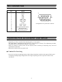
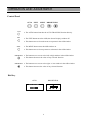
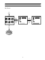
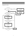
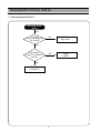
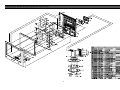
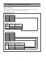
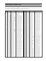
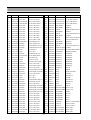
Service Manual
XGA COLOR MONITOR
Model : L510B1
DAEWOO ELECTRONICS CO., LTD.
http : //svc.dwe.co.kr
September, 2001
CONTENTS
SAFETY PRECAUTIONS
1
GENERAL SAFETY INFORMATION
2
SERVICING PRECAUTIONS
3
TECHNICAL INFORMATION
6
GENERAL INFORMATION
7
PIN CONNECTOR
8
CAUTIONS FOR ADJUSTMENT AND REPAIR
8
OPERATION & ADJUSTMENT
9
ALIGNMENT PROCEDURE
14
TROUBLESHOOTING HINTS
15
BLOCK DIAGRAM
22
PCB LAYOUT
23
SCHEMATIC DIAGRAM
27
EXPLODED VIEW & MECHANICAL PARTS LIST
29
INFORMATION OF PART DESCRIPTION
30
ELECTRICAL PARTS LIST
31
SAFETY PRECAUTIONS
CAUTION: No modifications of any circuits should be attempted. Service work should be performed
only after you are thoroughly familiar with all of the following safety checks and servicing
guidelines.
◆ Safety Check
Care should be taken while servicing the inverter that generates the high voltage to lighten CCFL of the
LCD panel.
◆ Fire & Shock Hazard
• Insert an isolation transformer between the analog color display and AC power line before servicing the
chassis.
• When servicing, pay close attention to the original lead dress especially in the high voltage circuit area;
if a short circuit is found, replace all parts which have been overheated as a result of the short circuit.
• All the protective devices must be reinstalled per original design.
• Soldering must be inspected for possible cold solder points, frayed leads, damaged insulation, solder
splashes or sharp solder points. Be certain to remove all foreign materials.
1
GENERAL SAFETY INFORMATION
◆ Terms in the manual
CAUTION
Statements identify conditions or practices that could result in damage to the equipment or
other property.
WARNING Statements identify conditions or practices that could result in personal injury or loss of
life.
◆ Terms as marked on equipment
CAUTION
Statements indicate a personal injury hazard not immediately accessible as one reads the
marking or a hazard which is properly included on the equipment itself.
WARNING Statements are clearly concerning indicated personal injury hazards.
◆ Symbols in the manual
The symbols indicate where applicable cautionary or other information is to be found.
◆ Symbols as marked on equipment
Protective GROUND terminal
◆ High Voltage Warning
And Critical Component Warning Label
The following warning label is on the inverter isolation case.
2
SERVICING PRECAUTIONS
CAUTION: Before servicing instruments covered by this service manual, its supplements, and
addendum, please read and follow the SAFETY PRECAUTIONS of this manual.
NOTE: If unforeseen circumstances create conflict between the following servicing precautions and any
of the safety precautions on page 1 of this manual, always follow the safety precautions.
Remember: Safety First.
◆ General Servicing Precautions
1. Always unplug the AC power cord from the AC power source before:
a. Removing or reinstalling any component, circuit board, module, or any other instrument assembly.
b. Disconnecting or reconnecting any electrical plug or other electrical connection.
c. Connecting a test substitute in parallel with an electrolytic capacitor in the instrument.
CAUTION: A wrong part substitution or incorrect polarity installation of electrolytic capacitors
may result in a explosion.
d. Discharging the picture tube anode.
2. Test high voltage only by measuring it with an appropriate high voltage meter or other voltage
measuring device (DVM, FETVOM. etc.) equipped with a suitable high voltage probe. Do not test high
voltage by “drawing an arc”.
3. Discharge the picture tube anode only by: (a) first connecting one end of an insulated clip lead to the
degaussing or line grounding system shield at the point where the picture tube socket ground lead is
connected, and then (b) touching the other end of the insulated clip lead to the picture tube anode
button, using an insulating handle to avoid personal contact with high voltage.
4. Do not any spray chemicals on or near this instrument, or any of its assemblies.
5. Unless otherwise specified in this service manual, only clean electrical contacts by applying the
following mixture to the contacts with a pipe cleaner, cotton-tipped stick, or comparable nonabrasive
applicator: 10% (by volume) Aceton and 90% (by volume) isopropyl alchohol (90%-99% strength).
CAUTION: This is a flammable mixture. Unless specified in this service manual, lubrication of
contacts is not required.
6. Do not apply AC power to this instrument and/or any other of its electrical assemblies unless all the
solid-state device heat sinks are correctly installed.
7. Always connect the test instrument ground lead to the appropriate instrument chassis ground before
connecting the test instrument positive lead. Always remove the test instrument ground lead last.
8. Only use the test fixtures specified in this service manual with this instrument.
3
◆ Electrostatically Sensitive (ES) Devices
Some semiconductor (solid state) devices can be damaged easily by static electricity.
Such components are commonly called Electrostatically Sensitive (ES) Devices.
The typical examples of ES devices are integrated circuits, some field-effect transistors, and
semiconductor “chip” components. The following techniques should be used to help reduce the incidence
of component damage caused by static electricity.
1. Immediately before handling any semiconductor component or semiconductor-equipped assembly,
wipe off any electrostatic charge on your body by touching any known earth ground. Alternatively,
obtain and wear a commercially available discharging wrist strap device which should be removed for
potential shock reasons prior to applying power to the unit under testing conditions.
2. After removing the electrical assembly equipped with ES devices, place the assembly on a conductive
surface such as aluminum foil to prevent electrostatic charge buildup or exposure to the assembly.
3. Only use a grounded-tip soldering iron to solder or unsolder ES devices.
4. Only use an anti-static type solder removal device. Some solder removal devices not classified as “antistatic” can generate enough electrical charges to damage ES devices.
5. Do not use freon-propelled chemicals. These can generate enough electrical charges to damage ES devices.
6. Do not remove a replacement ES device from its protective package until immediately before you are
ready to install it. (Most replacement ES devices are packaged with leads electrically shorted together
by conductive foam, aluminum foil, or comparable conductive material).
7. Immediately before removing the protective material from the leads of replacement ES devices, touch
the protective material to the chassis or circuit assembly into which the device will be installed.
CAUTION: Be sure that no power is applied to the chassis or circuit, and observe all other safety
precautions.
8. Minimize bodily movements when handling unpackaged replacement ES devices. (Otherwise harmful
motion such as the brushing together clothes fabric or the lifting your foot from a carpeted floor can
generate enough static electricity to damage ES devices).
◆ General Soldering Guidelines
1. Use a grounded-tip, low-wattage soldering iron with appropriate tip size and shape that will maintain
tip temperature between a 550°F-660°F (288°C-316°C) range.
2. Use an appropriate gauge of RMA resin-core solder composed of 60 parts tin/40 parts lead.
3. Keep the soldering iron tip clean.
4. Throughly clean the surface to be soldered. Use a small wire-bristle (0.5 inch or 1.25cm) brush with a
metal handle. Do not use freon-propelled spray-on cleaners.
5. Use the following soldering technique:
a. Allow the soldering iron tip to reach normal temperature (550°F to 660°F or 288°C to 316°C)
b. Hold the soldering iron tip and solder strand against the component lead until the solder melts.
c. Quickly move the soldering iron tip to the junction of the component lead and the printed circuit foil,
and hold it there until the solder flows onto and around both the component lead and the foil.
d. Closely inspect the solder area and remove any excess or splashed solder with a small wire-bristle brush.
CAUTION: Work quickly to avoid overheating the circuit board printed foil.
4
FIGURE 1. USE SOLDERING IRON TO PRY LEADS
◆ IC Removal/Replacement
Some utilized chassis circuit boards have slotted (oblong) holes through which the IC leads are inserted
and then bent flat against the circuit foil. When holes are slotted, the following technique should be used
to remove and replace the IC. When working with boards using the familiar round hole, use the standard
technique as outlined in paragraphs 5 on the page under the title of general soldering guidelines.
◆ Removal
1. Desolder and straighten each IC lead in one operation by gently prying up on the lead with the
soldering iron tip as the solder melts.
2. Draw away the melted solder with an anti-static suction-type solder removal device (or with
desoldering braid before removing the IC.
◆ Replacement
1. Carefully insert the replacement IC in the circuit board.
2. Carefully bend each IC lead against the circuit foil pad and solder it.
3. Clean the soldered areas with a small wire-bristle brush. (lt is not necessary to reapply acrylic coating
to the area).
◆ “Small-Signal” Discrete Transistor Removal/Replacement
1. Remove the defective transistor by clipping its leads as close as possible to the component body.
2. Bend the ends of each of three leads remaining on the circuit board into a “U” shape.
3. Bend the replacement transistor leads into a “U” shape.
4. Connect the replacement transistor leads to the corresponding leads extending from the circuit board
and crimp the “U” with long nose pliers to ensure metal-to-metal contact, then solder each connection.
◆ Power IC, Transistor or Devices Removal/Replacement
1. Heat and remove all solders from the device leads.
2. Remove the heatsink mounting screw (if applicable).
3. Carefully remove the device from the circuit board.
4. Insert new device in circuit board.
5. Solder each device lead and then clip off excess lead.
6. Replace heatsink.
5
◆ Diode Removal/Replacement
1. Remove defective diode by clipping its leads as close as possible to diode body.
2. Bend the two remaining leads perpendicularly to the circuit board.
3. Observing diode polarity, wrap each lead out of the new diode around the corresponding lead on the
circuit board.
4. Securely crimp each connection and solder it.
5. Inspect the solder joints of the two “original” leads on the circuit board copper side. If they are not
shiny, reheat them and apply additional solder if necessary.
TECHNICAL INFORMATION
Panel
Synchronization
Video Bandwidth
Max Resolution
Colors
Display Area
Input Signal
Size
Pixel Pitch
Viewing Angle
15-inch (38 cm) diagonal
0.297 x 0.297 mm
75°(Right/Left)
70°(up), 70°(down)
350:1 contrast ratio (typ)
250cd/m2 brightness (typ)
RGB vertical stripe
30 - 62 KHz
50 - 75 Hz
80 MHz
1024 x 768 a 75Hz
6 bit (With dithering 16.7M Colors)
304.1mm x 228.1mm
RGB analog (0.7Vp-p, 75ohms)
H/V separate (TTL)
15 pin mini D-Sub
DDC1/2B/CI
100-240 Vac, 50/60 Hz (Free Voltage)
25.5 W
390 x 396 x 205 mm (with stand)
390 x 325 x 70.5 mm (without stand)
4.6/6.1 Kg
10/13.2 lbs
EPA, VESA DPMS, Nutek Compliant
5° forward, 30° backward
90° leftward, rightward
10 ~ 40°C /50 ~ 104°F
Contrast Ratio
Brightness
Color Filter
Horizontal
Vertical
Video
Sync
Input Signal Connector
Plug and Play
Power Source
Power Consumption
Dimension-W x H x D
Weight(net/gross )
Power Saving
Tilt/Swivel Range
Tilt
Swivel
Operating Temperature
6
GENERAL INFORMATION
This TFT LCD monitor automatically scans all horizontal frequencies from 30KHz to 62KHz, and all
vertical frequencies from 50Hz to 75Hz. This TFT LCD monitor supports IBM PC, PC/XT, PC/AT, personal
System/2 (PS/2), Apple Macintosh, and compatible users crisp text and vivid color graphics display when
using the following graphics adapters : (VGA, Super VGA, VESA and XGA and Apple Macintosh Video
Card). And so, this TFT LCD monitor has a maximum horizontal resolution of 1024 dots and a maximum
vertical resolution of 768 lines for superior clarity of display.
By accepting analog signal inputs which level is zero to 0.7 Volts. This TFT LCD monitor can display and
262, 144 colors depending on the graphics adapter and software being used. (available used to 8 bit panel is
16.7M colors)
◆ Abbreviations
ADJ
AFC
TFT-LCD
CCFL
H.SYNC
OSC
P.S.U
PWA
R.G.B
V.Sync
ADC
Adjustment
Automatic Frequency Control
Thin Film Transistor Liquid Crystal Diplay
Cold Cathode Fluorescent Lamp
Horizontal Synchronization
Oscillator
Power Supply Unit
Printed Circuit Board Wiring Assembly
Red, Green, Blue
Vertical Synchronization
Analog Display Converter
7
PIN CONNECTOR
Pin
Signal
1
2
3
4
5
6
7
8
9
10
11
12
13
14
15
Red
Green
Blue
GND
GND
GND - Red
GND - Green
GND - Blue
+5Vdc
GND - H.Sync
GND - V.Sync
Bi-directional Data (SDA)
Horizontal Sync
Vertical Sync (VCLK)
Data Clock (SCL)
1
6
10
15
Arrangement of 15-pin D-sub connector
CAUTIONS FOR ADJUSTMENT AND REPAIR
• Degaussing is always required when adjusting purity or convergence.
• The white balance adjustment has been done by a color analyzer in factroy. The adjustment procedure,
described in the service manual is made by a visual check.
• Allow 20 minutes warm-up time for the display before checking or adjusting only electrical
specification or function.
• Reform the leadwire after any repair work.
◆ Caution For Servicing
• In case of servicing or replacing inverter, high voltage sometimes remains in the output of the inverter.
Completely discharge high voltage before servicing or replacing inverter to prevent a shock to the
serviceman.
8
OPERATION AND ADJUSTMENT
Control Panel
AUTO
AUTO
EXIT
MENU
BRIGHTNESS
BRIGHTNESS
EXIT
MENU
BRIGHTNESS
•
The AUTO button launches the AUTO TRACKING function directly.
•
•
The EXIT button turns the OSD (On-Screen Display) window off.
•
•
The MENU button turns the OSD window on.
•
•
The button moves cursor to the left or high window in the OSD window.
•
•
The button moves cursor to the right or low window in the OSD window.
This button moves from sub menu to top menu in the OSD window.
This button moves from top menu to sub menu in the OSD window.
This button decreases the value of any selected function.
This button increases the value of any selected function.
Hot Key
AUTO
BRIGHTNESS
AUTO TRACKING
9
Key Process
MENU
UT L TY
M E NU
U T L TY
OSD
OSD
MENU
UT L T Y
EXIT
MENU
SHARPNESS
EXIT
OSD OFF
10
EXIT
SHARPNESS
Adjustment Procedure
No
Is the H.Size
proper?
Adjust the CLOCK
control.
Yes
Is the
noise displayed on
the screen?
Perform the AUTO
POSITION.
No
Yes
Perform the AUTO
TRACKING.
Is the
noise displayed on
the screen yet?
No
Yes
Adjust the CLOCK FINE
until the screen is
cleared.
Yes
Is the
noise displayed on
the screen yet?
No
End
11
OSD Functions
ICON
CONTROL
FUNCTIONS
LANGUAGE
Select language for OSD (6 languages).
CLOCK
Adjust the width (horizontal size) of the screen image.
CLOCK FINE
Sharpen the focus by aligning the illuminated pixels and adjust until the
screen image looks focused, crisp and sharp. Adjusting the CLOCK
FINE after the CLOCK adjustment will produce a clear screen.
AUTO TRACKING
Adjust the horizontal & vertical picture image quality and size.
COLOR TEMP
Choose different preset color temperatures or set your own customized
color parameters.
R
RED CONTROL
Adjust the red color.
G
GREEN CONTROL
Adjust the green color.
B
BLUE CONTROL
Adjust the blue color.
H. CENTER &
V. CENTER
Adjust the position of the display horizontally(left or right) and
vertically (up or down).
SHARPNESS
Adjust the display image quality (if the screen proceed to scaling up).
OSD POSITION
Adjust the OSD position horizontally (left or right) and vertically (up or
down).
OSD
TIME OUT
Adjust the display OSD Menu.
STATUS
Display horizontal & vertical frequency and polarity.
RECALL
Reset the screen to the Factory Preset Display Settings.
AUTO POSITION
Choose automatically the proper horizontal position and vertical
position & size of the screen image.
CONTRAST
Adjust the contrast of image, the difference between light and dark
areas on the screen.
OSD
12
Self Diagnosis
When the monitor doesn’t display, if you press any key, Self Diagnosis screen is displayed. Self Diagnosis
function checks if the status of the monitor is No Signal or Out of range.
No Signal screen is displayed when the D-Sub signal connector is not connected or
the status of the monitor is on DPMS mode.
Out of Range screen is displayed when the applied frequency is under or over
normal range.
Normal range
(Non-interlaced mode only)
H : 30 - 62 KHz
V : 50 - 75 Hz
13
ALIGNMENT PROCEDURE
Standard Check point
1. Power source : 100 - 240Vac, 50/60Hz.
2. Aging : Take at least 20 minutes warm-up time.
3. Signal
Video input : Analog 0.7Vpp 75Ω terminal positive polarity
Synchronizing : acceptable negative or positive at TTL level
Max. Resolution : 1024 x 768 a 75Hz
Frequency
Horizontal : 30KHz - 62KHz
Vertical : 50Hz - 75Hz (available only non interlace mode)
Adjustment
1. Smart scaling set to 69%.
2. Contrast set to 90%
3. Brightness set to 50%
4. Switching to factory alignment mode
Press power key with Brightness left key at the power off status.
5. Video level adjustment
Receive stair pattern of 16 step (doesn’t care any mode).
Readjust coarse R, G, B in TDA8752 menu before saturaton point.
6. Set up the tracking
See the user’s manual at page 8th.
7. Switching to user’s mode
If turn-off and turn-on then switched to user’s mode.
* All of adjusted data stores by fade out of OSD.
14
TROUBLESHOOTING HINTS
1. Abnormal mode detect
Abnormal mode
detect
Yes
Is a input
H-sync of ADC(pin 90,
U2) correct?
No
Trouble in the H-sync
input circuit.
No
Trouble
in ADC.
Yes
Is waveform
of pin 81 of ADC(U2)
correct?
Yes
Trouble
in Scaler(U1).
15
2. Trouble in Power on
Is the
Power LED toggled
between on and
off?
On
Refer to No video
or No raster.
Off
Is the power
cord well
connected?
No
Check if the power switch
is on position and
Connect the power
cord correctly.
Yes
Check the
waveform of pin 7
of -com.
No
Trouble in U6 & Q5
and its ambient circuit.
No
Check the power board
(5VS of CN2A).
Yes
Is 5VS line
normal(pin 8 of CN2)?
Yes
Check on Scaler(U1).
16
3. No Raster
Check the
output of Q2 or
pin 3 of U3.
< 2.5
Trouble in Q6 or
pin 3 of -com.
> 2.5
Is 12V
plugged in pin 1
of CN4A(power
board)?
No
Check the output
of D811(power board).
Yes
Is the output of
inverter correct?
No
Yes
Replace a LCD panal.
17
Replace the inverter.
4. One color is missing
One color is missing
Yes
No
Is the OSD color
normal?
Check the output
signal of Scaler.
Yes
Is the input
signal normal?
No
Check the video signal
cable or R,G,B
con-ass’y.
Yes
Are the
R,G,B Digital values
(every eight bits) correct
on ADC output
stage?
Yes
Trouble in the soldering
of R,G,B data lines
from output of ADC
to Scaler(U1).
18
No
Check the ambient
circuit of ADC.
5. No Video
Has display image
only white?
No
Next page.
Yes
Check if
the CN5 wafer is
well connected at
the LCD panel.
No
Connection trouble.
Yes
Is pin 1
of Q6 3.3V?
No
Yes
Check the output of scalier
(pin 71, 72, 73, 74, 75)
and soldering of CN5.
19
Check Q6, its ambient
circuit and pin 27 of -com.
5-1. No Video
Black
Yes
Is OSD normal?
No
3. No raster
or Check SDRAM.
No
Set the contrast
up to Max.
Yes
Is the contrast
at its maximum?
Yes
Is the output of
ADC correct?
No
Is the input of
ADC correct?
Yes
Yes
Next Page.
No
Check the video
input signal.
Replace the main board
(or replace ADC).
Yes
Is the output
of Scaler correct?
No
Is the input of
Scaler correct?
No
Yes
Yes
Replace the main board
(or replace ADC).
Check If
the CN5 wafer is
well connected at
the LCD panel.
20
6. Power Problem
Is the power
cord well
connected?
Check if the power
cord is correctly
connected.
No
Yes
Check 5VS, 5VD,
5VA, 6V, 3.3V
of CN2A.
No
Is
the output of
D812 6.2V?
Yes
No
Yes
Check the main board.
Check ambient
circuit of IC801.
21
22
PLL
Clock timing
& phase
3
TDA8752
3
Inverter On/Off
Dimming Control
Power on/off
H sync
Dot clock
I2C bus
B(6bit)
ADI
8
OSD
+12V
Dimming control
Inverter On/Off
Address & data
line(8bit)
Micom
(MTV212M)
+5V, +6V, +3.3V
Clamp
Controller
Scalar
12 12 12
I2C bus
12MHz
EEPROM
Output Video Rate
-H: 48~62kHz, V:60~75Hz
-Resolution: only 1024*768
-Dot clock: 65~80MHz
Red(E/O)
Green(E/O)
Blue(E/O)
H sync, V sync,
DE & dot clock
G(6bit)
ASI320
14.318MHz
R(6bit)
Mainbord Control
Power Board
Sampling
clock
ADC
Controller
Offset & amplifier
Current &
resistance
R,G,B
PRE-AMP
3
AC input rate
-Voltage: 100~240Vac
-Frequency: 50/60Hz
V sync
H sync
Buffer
(74ACT14)
2
H/V sync
15PIN DSUB
Input Video Rate
- H: 30~62kHz, V: 56~75Hz Resolution: up to 1024*768
Panel
DC-AV
inverter
650Vac
50KHz
Back
light
Panel
dirver
+3.3V
BLOCK DIAGRAM
PCB LAYOUT
Main PCB Component Side
Main PCB Solder Side
23
24
Control PCB Component Side
Control PCB Solder Side
25
Power & D-Sub PCB Component Side
Power & D-Sub PCB Solder Side
26
SCHEMATIC DIAGRAM
Main Section
27
SMPS Section
28
EXPLODED VIEW & MECHANICAL PARTS LIST
29
INFORMATION OF PART DESCRIPTION
Important Safety Notice
Components identified with the International Symbol have special characteristics important for safety.
When replacing any components, use only manufacturer’s specified parts.
Abbreviation of Description
RESISTOR Description
Tolerance
F
± 1%
J
± 5%
K
± 10%
M
± 20%
G
± 2%
Example:
Fig &
Index
Part No
Description
Resistors
RD-4Z820J
Carbon : 82J
HRFS472JBA Chip 4.7K OHM J
R101
R30
CAPACITOR Description
C
D
F
J
K
P
Z
Tolerance
± 0.25pF
± 0.5%
± 1pF
± 5%
± 10%
± 100% ~ 0%
± 80% ~ –
Example:
Fig &
Index
C28
C63
C44
Part No
Description
Capacitors
HCFK104ZBA
Chip Cera 50V Z
HCBK393KBA
Chip Cera 50V K
HCQK102JBA
Chip Cera 50V J
30
ELECTRICAL PARTS LIST
The components identified by mark
have special characteristics important for safety and x-ray radiation.
These should be replaced only with the types specified in the parts list.
LOC
PART-CODE
PART-NAME
00020 W3415M731- CORD POWER
PART-DESC
LOC
PART-CODE
PART-NAME
PART-DESC
C5 H03VV-F 3X0.75 1.8M BK
C29
HCFF474ZBA C CHIP CERA
Y5V 16V 0.47MF Z 1608
00040 9970800035
CABLE SIGNAL AS 15P+15P/DDC=1.5M(GY275A)
C3
HCBK103KBA C CHIP CERA
50V X7R 0.01MF K 1608
B801
5PB13857--
COIL BEAD
BI3857(AXIAL)
C30
HCBK102KBA C CHIP CERA
50V X7R 1000PF K 1608
C1
HCQK100JBA C CHIP CERA
50V CH 10PF J 1608
C31
HCFK104ZBA C CHIP CERA
50V Y5V 0.1MF Z 1608
C10
HCBK223KBA C CHIP CERA
50V X7R 0.022MF K 1608
C32
HCFK104ZBA C CHIP CERA
50V Y5V 0.1MF Z 1608
C101 HCENH101MD C CHIP ELECTRO
MV 25V 100MF D8.0XH6.3
C33
HCFK104ZBA C CHIP CERA
50V Y5V 0.1MF Z 1608
C102 HCENH101MD C CHIP ELECTRO
MV 25V 100MF D8.0XH6.3
C34
HCFK104ZBA C CHIP CERA
50V Y5V 0.1MF Z 1608
C103 HCENH101MD C CHIP ELECTRO
MV 25V 100MF D8.0XH6.3
C35
HCQK150JBA C CHIP CERA
50V CH 15PF J 1608
C104 HCEKF100MC C CHIP ELECTRO
MV 16V 10MF D4.0XH5.2
C36
HCFK104ZBA C CHIP CERA
50V Y5V 0.1MF Z 1608
C105 HCEKF100MC C CHIP ELECTRO
MV 16V 10MF D4.0XH5.2
C37
HCFK104ZBA C CHIP CERA
50V Y5V 0.1MF Z 1608
C106 HCBK102KBA C CHIP CERA
50V X7R 1000PF K 1608
C38
HCFK104ZBA C CHIP CERA
50V Y5V 0.1MF Z 1608
C107 HCFF474ZBA C CHIP CERA
Y5V 16V 0.47MF Z 1608
C39
HCFK104ZBA C CHIP CERA
50V Y5V 0.1MF Z 1608
C108 HCFK104ZBA C CHIP CERA
50V Y5V 0.1MF Z 1608
C4
HCFK104ZBA C CHIP CERA
50V Y5V 0.1MF Z 1608
C109 HCFK104ZBA C CHIP CERA
50V Y5V 0.1MF Z 1608
C40
HCFF474ZBA C CHIP CERA
Y5V 16V 0.47MF Z 1608
C11
HCFK104ZBA C CHIP CERA
50V Y5V 0.1MF Z 1608
C41
HCFK104ZBA C CHIP CERA
50V Y5V 0.1MF Z 1608
C110 HCFK104ZBA C CHIP CERA
50V Y5V 0.1MF Z 1608
C42
HCQK151JBA C CHIP CERA
50V CH 150PF J 1608
C111 HCFK104ZBA C CHIP CERA
50V Y5V 0.1MF Z 1608
C43
HCBK393KBA C CHIP CERA
50V X7R 0.039MF K 1608
C112 HCEKF100MC C CHIP ELECTRO
MV 16V 10MF D4.0XH5.2
C44
HCFK104ZBA C CHIP CERA
50V Y5V 0.1MF Z 1608
C113 HCEKF100MC C CHIP ELECTRO
MV 16V 10MF D4.0XH5.2
C45
HCFK104ZBA C CHIP CERA
50V Y5V 0.1MF Z 1608
C114 HCEDC470MC C CHIP ELECTRO
MV 6.3V 47MF 5DX5.2H
C46
HCQK120JBA C CHIP CERA
50V CH 12PF J 1608
C115 HCFK104ZBA C CHIP CERA
50V Y5V 0.1MF Z 1608
C47
HCQK120JBA C CHIP CERA
50V CH 12PF J 1608
C116 HCFD105ZBA C CHIP CERA
Y5V 10V 1MF Z 1608
C48
HCQK120JBA C CHIP CERA
50V CH 12PF J 1608
C117 HCBK102KBA C CHIP CERA
50V X7R 1000PF K 1608
C49
HCQK120JBA C CHIP CERA
50V CH 12PF J 1608
C118 HCBK102KBA C CHIP CERA
50V X7R 1000PF K 1608
C5
HCBK103KBA C CHIP CERA
50V X7R 0.01MF K 1608
C119 HCFF474ZBA C CHIP CERA
Y5V 16V 0.47MF Z 1608
C50
HCENH101MD C CHIP ELECTRO
MV 25V 100MF D8.0XH6.3
C12
50V X7R 0.01MF K 1608
C51
HCEKF100MC C CHIP ELECTRO
MV 16V 10MF D4.0XH5.2
50V Y5V 0.1MF Z 1608
C52
HCFK104ZBA C CHIP CERA
50V Y5V 0.1MF Z 1608
HCBK103KBA C CHIP CERA
C120 HCFK104ZBA C CHIP CERA
C13
HCFK104ZBA C CHIP CERA
50V Y5V 0.1MF Z 1608
C53
HCFK104ZBA C CHIP CERA
50V Y5V 0.1MF Z 1608
C14
HCBK103KBA C CHIP CERA
50V X7R 0.01MF K 1608
C54
HCEKF100MC C CHIP ELECTRO
MV 16V 10MF D4.0XH5.2
C15
HCBK223KBA C CHIP CERA
50V X7R 0.022MF K 1608
C55
HCQK221JBA C CHIP CERA
50V CH 220PF J 1608
C16
HCBK103KBA C CHIP CERA
50V X7R 0.01MF K 1608
C56
HCFK104ZBA C CHIP CERA
50V Y5V 0.1MF Z 1608
C17
HCBK223KBA C CHIP CERA
50V X7R 0.022MF K 1608
C57
HCEKF100MC C CHIP ELECTRO
MV 16V 10MF D4.0XH5.2
C18
HCFK104ZBA C CHIP CERA
50V Y5V 0.1MF Z 1608
C58
HCQK100JBA C CHIP CERA
50V CH 10PF J 1608
C19
HCBK223KBA C CHIP CERA
50V X7R 0.022MF K 1608
C59
HCQK151JBA C CHIP CERA
50V CH 150PF J 1608
C2
HCBK103KBA C CHIP CERA
50V X7R 0.01MF K 1608
C6
HCBK223KBA C CHIP CERA
50V X7R 0.022MF K 1608
C20
HCBK103KBA C CHIP CERA
50V X7R 0.01MF K 1608
C60
HCFK104ZBA C CHIP CERA
50V Y5V 0.1MF Z 1608
C21
HCBK223KBA C CHIP CERA
50V X7R 0.022MF K 1608
C61
HCEDC470MC C CHIP ELECTRO
MV 6.3V 47MF 5DX5.2H
C22
HCFK104ZBA C CHIP CERA
50V Y5V 0.1MF Z 1608
C62
HCEDC470MC C CHIP ELECTRO
MV 6.3V 47MF 5DX5.2H
C23
HCBK102KBA C CHIP CERA
50V X7R 1000PF K 1608
C63
HCEDC470MC C CHIP ELECTRO
MV 6.3V 47MF 5DX5.2H
C24
HCFK104ZBA C CHIP CERA
50V Y5V 0.1MF Z 1608
C64
HCEDC470MC C CHIP ELECTRO
MV 6.3V 47MF 5DX5.2H
C25
HCBK102KBA C CHIP CERA
50V X7R 1000PF K 1608
C65
HCEDC470MC C CHIP ELECTRO
MV 6.3V 47MF 5DX5.2H
C26
HCFK104ZBA C CHIP CERA
50V Y5V 0.1MF Z 1608
C66
HCEDC470MC C CHIP ELECTRO
MV 6.3V 47MF 5DX5.2H
C27
HCBK102KBA C CHIP CERA
50V X7R 1000PF K 1608
C67
HCEDC470MC C CHIP ELECTRO
MV 6.3V 47MF 5DX5.2H
C28
HCFK104ZBA C CHIP CERA
50V Y5V 0.1MF Z 1608
C68
HCEDC470MC C CHIP ELECTRO
MV 6.3V 47MF 5DX5.2H
31
LOC
PART-CODE
PART-NAME
PART-DESC
LOC
PART-CODE
PART-NAME
PART-DESC
C69
HCEDC470MC C CHIP ELECTRO
MV 6.3V 47MF 5DX5.2H
C96
HCEKF100MC C CHIP ELECTRO
MV 16V 10MF D4.0XH5.2
C7
HCFK104ZBA C CHIP CERA
50V Y5V 0.1MF Z 1608
C70
HCEDC470MC C CHIP ELECTRO
MV 6.3V 47MF 5DX5.2H
C97
HCEKF100MC C CHIP ELECTRO
MV 16V 10MF D4.0XH5.2
C98
HCEDC470MC C CHIP ELECTRO
MV 6.3V 47MF 5DX5.2H
C71
HCEKF100MC C CHIP ELECTRO
MV 16V 10MF D4.0XH5.2
C99
HCEDC470MC C CHIP ELECTRO
MV 6.3V 47MF 5DX5.2H
C72
HCFK104ZBA C CHIP CERA
50V Y5V 0.1MF Z 1608
CN1
9979220119
CONN WAFER
YDW200-12
C73
HCFK104ZBA C CHIP CERA
50V Y5V 0.1MF Z 1608
CN10 9979220013
CONN WAFER
SMW250-12
C74
HCFK104ZBA C CHIP CERA
50V Y5V 0.1MF Z 1608
CN1A 99707C0013
CONN AS
SMH250+YDH200+2990=360
C75
HCFK104ZBA C CHIP CERA
50V Y5V 0.1MF Z 1608
CN2
CONN WAFER
YDW200-10
C76
HCFK104ZBA C CHIP CERA
50V Y5V 0.1MF Z 1608
CN2A 99707A0024
CONN AS
35164+YDH200+2464#24=150
C77
HCFK104ZBA C CHIP CERA
50V Y5V 0.1MF Z 1608
CN3
CONN WAFER
YDW200-04
C78
HCFK104ZBA C CHIP CERA
50V Y5V 0.1MF Z 1608
CN3A 9970740046
CONN AS
SMH250+YDH200+1007#24=330
C8
HCBK102KBA C CHIP CERA
9979220118
9979220117
50V X7R 1000PF K 1608
CN4A 9970750037
CONN AS
5264+35164+2464#24=135
C801 CL1GB3334M C LINE ACROSS
U/C/V/S/N/D/E/SV 250V
CN5
9979220148
CONN WAFER
FX8-80P-SV
C802 CEYP2G680Z C ELECTRO
400V SLT 68MF (25*20)
CN6
9979200203
CONN WAFER
YW396-03AV
C803 CEXF1C101V C ELECTRO
16V RSS 100MF (6.3X11) TP
CN6A 9970720083
CONN AS
1015#18+35404-9002*4=120
C805 CEXF1H330V C ELECTRO
50V RSS 33MF (6.3X11) TP
CN7
9979200317
SOCKET AC INLET ST-03B-BP
C807 CCYB3A103K C CERA
1KV B 0.01MF K
CN8
9979200209
D-SUB 15P ANGLE 15P DDC BLUE W/IN SCREW
C808 CCXF1H104Z C CERA
50V F 0.1MF Z
CN9
9979220019
CONN WAFER
C809 CEXF1H109V C ELECTRO
50V RSS 1MF (5X11) TP
D1
DKDS226RTK DIODE CHIP
KDS226(RTK)
C81
MV 16V 10MF D4.0XH5.2
D2
DKDS226RTK DIODE CHIP
KDS226(RTK)
C811 CMXM2A103J C MYLAR
100V 0.01MF J (TP)
D3
DKDS226RTK DIODE CHIP
KDS226(RTK)
C812 CXSL3A470K C CERA
1KV SL 47PF K (TP)
D4
DKDS226RTK DIODE CHIP
KDS226(RTK)
C813 CCXB1H681K C CERA
50V B 680PF K (TAPPING)
D5
DKDS226RTK DIODE CHIP
KDS226(RTK)
C82
HCEKF100MC C CHIP ELECTRO
SMAW250-04 (ANGLE)
HCFK104ZBA C CHIP CERA
C824 CH1FDF103M C CERA AC
50V Y5V 0.1MF Z 1608
D6
DKDS226RTK DIODE CHIP
KDS226(RTK)
2.5KV 0.01MF M AC250V
D7
DKDS226RTK DIODE CHIP
KDS226(RTK)
DRLS4148--
50V Y5V 0.1MF Z 1608
D8
DIODE CHIP
RLS4148
C835 CEXF1E102V C ELECTRO
25V RSS 1000MF (13X20) BK
D801 DD3SBA60--
DIODE
D3SBA60
C838 CEXF1C471V C ELECTRO
16V RSS 470MF (10X12.5)BK
D805 DZN4148---
DIODE
1N4148 AUTO 52MM
C84
50V Y5V 0.1MF Z 1608
D807 DSUF4007SP DIODE
C843 CCXF1H104Z C CERA
50V F 0.1MF Z
D809 DUG2D-----
C844 CCXF1H104Z C CERA
50V F 0.1MF Z
D811 DFMLG22S-- DIODE
C845 CEXF1C102V C ELECTRO
16V RSS 1000MF (10X20) TP
D812 DUG2D-----
DIODE
UG2D 200V 2A
C848 CEXF1H109V C ELECTRO
50V RSS 1MF (5X11) TP
D812A DUG2D-----
DIODE
UG2D 200V 2A
C83
C85
HCFK104ZBA C CHIP CERA
HCFK104ZBA C CHIP CERA
HCFK104ZBA C CHIP CERA
DIODE
SUF4007SP
UG2D 200V 2A
FML-G22S
50V Y5V 0.1MF Z 1608
D813 DFMBG19L-- DIODE
FMB-G19L
C850 CEXF1C471V C ELECTRO
16V RSS 470MF (10X12.5)BK
D9
RLS4148
C851 CEXF1C471V C ELECTRO
16V RSS 470MF (10X12.5)BK
DZ12 DRLZ5R6B-B DIODE CHIP ZENER RLZTE-11 5.6B
C855 CEXF1C471V C ELECTRO
16V RSS 470MF (10X12.5)BK
DZ13 DRLZ5R6B-B DIODE CHIP ZENER RLZTE-11 5.6B
C859 CEXF1E101V C ELECTRO
25V RSS 100MF (6.3X11) TP
DZ803 DDZ22BM---
DIODE ZENER
DZ22BM
C86
HCFK104ZBA C CHIP CERA
50V Y5V 0.1MF Z 1608
DZ806 DGDZJ18C--
DIODE ZENER
GDZJ 18C
C87
HCFK104ZBA C CHIP CERA
50V Y5V 0.1MF Z 1608
DZ813 DDZ5R1B---
DIODE ZENER
DZ-5.1B
C88
HCFK104ZBA C CHIP CERA
50V Y5V 0.1MF Z 1608
DZ814 DDZ5R1B---
DIODE ZENER
DZ-5.1B
DRLS4148--
DIODE CHIP
C89
HCFK104ZBA C CHIP CERA
50V Y5V 0.1MF Z 1608
DZ815 DDZ5R1B---
DIODE ZENER
DZ-5.1B
C9
HCBK103KBA C CHIP CERA
50V X7R 0.01MF K 1608
F801
FUSE CERA
SEMKO TL 3.15AH 250V MF51
C90
HCFK104ZBA C CHIP CERA
50V Y5V 0.1MF Z 1608
F801A 9977410900
FUSE CLIP
BSP3-H T0.4 SN 5.2
C91
HCFK104ZBA C CHIP CERA
50V Y5V 0.1MF Z 1608
F801B 9977410900
FUSE CLIP
BSP3-H T0.4 SN 5.2
C92
HCFK104ZBA C CHIP CERA
50V Y5V 0.1MF Z 1608
FB1
HFFTB2601B COIL CHIP BEAD
TB321611Z260
C93
HCEKF100MC C CHIP ELECTRO
MV 16V 10MF D4.0XH5.2
FB10 HFFTB2601B COIL CHIP BEAD
TB321611Z260
C94
HCFK104ZBA C CHIP CERA
50V Y5V 0.1MF Z 1608
FB11 HFFTB2601B COIL CHIP BEAD
TB321611Z260
32
5F3CB3122L
LOC
PART-CODE
PART-NAME
PART-DESC
LOC
PART-CODE
PART-NAME
PART-DESC
FB12 HFFTB2601B COIL CHIP BEAD
TB321611Z260
R2
HRFS472JBA R CHIP
1/16 4.7K OHM J 1608
FB13 HFFTB2601B COIL CHIP BEAD
TB321611Z260
R20
HRFS472JBA R CHIP
1/16 4.7K OHM J 1608
FB14 HFFTB2601B COIL CHIP BEAD
TB321611Z260
R21
HRFS472JBA R CHIP
1/16 4.7K OHM J 1608
FB15 HFFTB2601B COIL CHIP BEAD
TB321611Z260
R22
HRFS472JBA R CHIP
1/16 4.7K OHM J 1608
FB16 HFFTB2601B COIL CHIP BEAD
TB321611Z260
R23
HRFS472JBA R CHIP
1/16 4.7K OHM J 1608
FB17 HFFTB2601B COIL CHIP BEAD
TB321611Z260
R24
HRFS472JBA R CHIP
1/16 4.7K OHM J 1608
FB18 HFFTB2601B COIL CHIP BEAD
TB321611Z260
R25
HRFS472JBA R CHIP
1/16 4.7K OHM J 1608
FB19 HFFTB2601B COIL CHIP BEAD
TB321611Z260
R26
HRFS472JBA R CHIP
1/16 4.7K OHM J 1608
FB2
HFFTB2601B COIL CHIP BEAD
TB321611Z260
R29
HRFS220JBA R CHIP
1/16W 22 OHM J 1608
FB20 HFFTB2601B COIL CHIP BEAD
TB321611Z260
R3
HRFS101JBA R CHIP
1/16 100 OHM J 1608
FB3
HFFTB2601B COIL CHIP BEAD
TB321611Z260
R30
HRFS472JBA R CHIP
1/16 4.7K OHM J 1608
FB4
HFFTB2601B COIL CHIP BEAD
TB321611Z260
R31
HRFS101JBA R CHIP
1/16 100 OHM J 1608
FB7
HFFTB2601B COIL CHIP BEAD
TB321611Z260
R32
HRFS101JBA R CHIP
1/16 100 OHM J 1608
FB8
HFFTB2601B COIL CHIP BEAD
TB321611Z260
R33
HRFS221JBA R CHIP
1/16 220 OHM J 1608
FB9
HFFTB2601B COIL CHIP BEAD
TB321611Z260
R34
HRFS472JBA R CHIP
1/16 4.7K OHM J 1608
IC801 1KA3842B--
IC POWER
KA3842B
R35
HRFS472JBA R CHIP
1/16 4.7K OHM J 1608
IC802 1KA78R05--
IC REGULATOR
KA78R05
R36
HRFS472JBA R CHIP
1/16 4.7K OHM J 1608
IC803 1KA278R33-
IC REGULATOR
KA278R33
R37
HRFS221JBA R CHIP
1/16 220 OHM J 1608
IC804 1TLP721GR-
IC PHOTO COUPLER TLP721D4GR
R38
HRFS472JBA R CHIP
1/16 4.7K OHM J 1608
IC805 1KA431ZTA-
IC SHUNT
KA431ZTA
R39
HRFS472JBA R CHIP
1/16 4.7K OHM J 1608
IC811 1KA78R05--
IC REGULATOR
KA78R05
R4
HRFS223JBA R CHIP
1/16 22K OHM J 1608
LCD INVERTER
FLI-1501
R40
HRFS102JBA R CHIP
1/16 1K OHM J 1608
FILTER LINE
DLF-2323
R41
HRFS102JBA R CHIP
1/16 1K OHM J 1608
! INV1 DFL11501-L801
5PDLF2323-
L811
5MC0000003 COIL CHOKE
L-82
R42
HRFS472JBA R CHIP
1/16 4.7K OHM J 1608
LCD
9979615042
L150X2M
R43
HRFS101JBA R CHIP
1/16 100 OHM J 1608
LED1 DSD50GYW-- LED
SD50GYW(GREEN/AMBER)
R44
HRFS101JBA R CHIP
1/16 100 OHM J 1608
PCB1 9979800571
PCB MAIN
T=1.6*138*100 (L510B1)
R45
HRFS000JBA R CHIP
1/16 0 OHM J 1608
PCB2 9979800560
PCB POWER
T=1.6*162*102.5(L510B)
R46
HRFS472JBA R CHIP
1/16 4.7K OHM J 1608
PCB3 9979800566
PCB CONTROL
T=1.6*246*122
R47
HRFS750JBA R CHIP
1/16W 75 OHM J 1608
LCD PANEL
Q1
TKTC3875SY TR CHIP
KTC3875SY(RTK)
R48
HRFS750JBA R CHIP
1/16W 75 OHM J 1608
Q2
TKTC3875SY TR CHIP
KTC3875SY(RTK)
R49
HRFS750JBA R CHIP
1/16W 75 OHM J 1608
Q3
TKTC3875SY TR CHIP
KTC3875SY(RTK)
R50
HRFS101JBA R CHIP
1/16 100 OHM J 1608
Q4
TKTC3875SY TR CHIP
KTC3875SY(RTK)
R51
HRFS101JBA R CHIP
1/16 100 OHM J 1608
Q5
TKTC3875SY TR CHIP
KTC3875SY(RTK)
R52
HRFS472JBA R CHIP
1/16 4.7K OHM J 1608
Q6
TNDS9958--
NDS9958
R53
HRFS472JBA R CHIP
1/16 4.7K OHM J 1608
Q801 TSSS6N70A- FET
SSS6N70A
R54
HRFS512JBA R CHIP
1/16 5.1K OHM J 1608
Q802 TZTC3198Y-
TR
KTC3198Y-(1815Y) (AUTO)
R56
HRFS472JBA R CHIP
1/16 4.7K OHM J 1608
Q810 TZTC3202Y-
TR
FET CHIP
KTC3202Y (AUTO)(1959Y)
R57
HRFS472JBA R CHIP
1/16 4.7K OHM J 1608
R1
HRFS105JBA R CHIP
1/16 1M OHM J 1608
R58
HRFS472JBA R CHIP
1/16 4.7K OHM J 1608
R10
HRFS101JBA R CHIP
1/16 100 OHM J 1608
R59
HRFS472JBA R CHIP
1/16 4.7K OHM J 1608
R11
HRFS101JBA R CHIP
1/16 100 OHM J 1608
R60
HRFS472JBA R CHIP
1/16 4.7K OHM J 1608
R12
HRFS153JBA R CHIP
1/16 15K OHM J 1608
R61
HRFS472JBA R CHIP
1/16 4.7K OHM J 1608
R13
HRFS102JBA R CHIP
1/16 1K OHM J 1608
R63
HRFS105JBA R CHIP
1/16 1M OHM J 1608
R14
HRFS472JBA R CHIP
1/16 4.7K OHM J 1608
R64
HRFS102JBA R CHIP
1/16 1K OHM J 1608
R16
HRFS102JBA R CHIP
1/16 1K OHM J 1608
R65
HRFS102JBA R CHIP
1/16 1K OHM J 1608
R17
HRFS102JBA R CHIP
1/16 1K OHM J 1608
R66
HRFS102JBA R CHIP
1/16 1K OHM J 1608
R18
HRFS472JBA R CHIP
1/16 4.7K OHM J 1608
R67
HRFS220JBA R CHIP
1/16W 22 OHM J 1608
R19
HRFS472JBA R CHIP
1/16 4.7K OHM J 1608
R68
HRFS472JBA R CHIP
1/16 4.7K OHM J 1608
33
LOC
PART-CODE
PART-NAME
PART-DESC
LOC
PART-CODE
PART-NAME
PART-DESC
R69
HRFS472JBA R CHIP
1/16 4.7K OHM J 1608
RP14 HRTS8E220J R CHIP ARRAY
1/16 8P 22 OHM J 3216
R72
HRFS102JBA R CHIP
1/16 1K OHM J 1608
RP15 HRTS8E220J R CHIP ARRAY
1/16 8P 22 OHM J 3216
R73
HRFS102JBA R CHIP
1/16 1K OHM J 1608
RP16 HRTS8E220J R CHIP ARRAY
1/16 8P 22 OHM J 3216
R80
RD-AZ302J-
R CARBON FILM
1/6 3K OHM J
RP17 HRTS8E220J R CHIP ARRAY
1/16 8P 22 OHM J 3216
R801 RD-2Z684J-
R CARBON FILM
1/2 680K OHM J
RP18 HRTS8E220J R CHIP ARRAY
1/16 8P 22 OHM J 3216
R803 RS01Z513J-
R M-OXIDE FILM
1W 51K OHM J
RP19 HRTS8E220J R CHIP ARRAY
1/16 8P 22 OHM J 3216
R804 RS01Z513J-
R M-OXIDE FILM
1W 51K OHM J
RP2
HFFH4M301E COIL CHIP BEAD
HB-4M3216-301JT
R805 RD-AZ102J-
R CARBON FILM
1/6 1K OHM J
RP3
HFFH4M301E COIL CHIP BEAD
HB-4M3216-301JT
R806 RD-AZ333J-
R CARBON FILM
1/6 33K OHM J
RP4
HFFH4M301E COIL CHIP BEAD
HB-4M3216-301JT
R807 RN-AZ2001F
R METAL FILM
1/6 2.0K OHM F
RP5
HFFH4M301E COIL CHIP BEAD
HB-4M3216-301JT
R809 RS01Z683J-
R M-OXIDE FILM
1W 68K OHM J (TAPPING)
RP6
HFFH4M301E COIL CHIP BEAD
HB-4M3216-301JT
R81
RD-AZ682J-
R CARBON FILM
1/6 6.8K OHM J
RP7
HFFH4M301E COIL CHIP BEAD
HB-4M3216-301JT
R812 RD-AZ470J-
R CARBON FILM
1/6 47 OHM J
RP8
HFFH4M301E COIL CHIP BEAD
HB-4M3216-301JT
R813 RD-AZ223J-
R CARBON FILM
1/6 22K OHM J
RP9
HFFH4M301E COIL CHIP BEAD
HB-4M3216-301JT
R814 RD-AZ102J-
R CARBON FILM
1/6 1K OHM J
SW1
5S50101Z10
SW TACT
KPT-1115AM
R815 RW01Z758JN R WIRE WOUND
R82
1W 0.75 OHM J NON-INDUCT
SW2
5S50101Z10
SW TACT
KPT-1115AM
RD-AZ153J-
R CARBON FILM
1/6 15K OHM J
SW3
5S50101Z10
SW TACT
KPT-1115AM
R820 RD-AZ180J-
R CARBON FILM
1/6 18 OHM J
SW4
5S50101Z10
SW TACT
KPT-1115AM
R822 RD-AZ681J-
R CARBON FILM
1/6 680 OHM J
SW5
5S50101Z10
SW TACT
KPT-1115AM
SW TACT
R825 RD-AZ479J-
R CARBON FILM
1/6 4.7 OHM J
SW6
5S50101Z10
R826 RD-AZ333J-
R CARBON FILM
1/6 33K OHM J
T801
5RM0000111 TRANS SMPS
KPT-1115AM
DMT-510B
R827 RD-AZ151J-
R CARBON FILM
1/6 150 OHM J
TH801 DTP8D13---
THERMISTOR
R83
RD-AZ303J-
R CARBON FILM
1/6 30K OHM J
U1
IC LCD CONTROLLER AS1320
R832 RD-AZ102J-
R CARBON FILM
1/6 1K OHM J
U2
1TDA8752BH IC ADC
TDA8752BH/8
R837 RD-AZ102J-
R CARBON FILM
1/6 1K OHM J
U3
1MTV212MV- IC MICOM
MTV212MV64I
1AS1320---
R839 RN-AZ1002F
R METAL FILM
1/6 10K OHM F
U3S
9979300502
R84
R CARBON FILM
1/6 62K OHM J
U4
1CAT24WC08 IC EEPROM
CAT24WC08 J
RD-AZ623J-
SOCKET IC
TP8D13
PLCC 1.27PT 44PIN(22*22)
R840 RN-AZ6651F
R METAL FILM
1/6 6.65K OHM F
U5
174ACT14SC IC INVERTER
74ACT14SCX
R841 RD-AZ102J-
R CARBON FILM
1/6 1K OHM J
U6
1K1A7042AF IC RESET
KIA7042AF
R854 RD-AZ102J-
R CARBON FILM
1/6 1K OHM J
U7
1LM385M25-
R855 RD-4Z512J-
R CARBON FILM
1/4 5.1K OHM J
Y1
5XS14R318F CRYSTAL QUARTZ HC-49/SM5H 14.318MHZ 18PF
HFFH4M301E COIL CHIP BEAD
HB-4M3216-301JT
Y2
5XJ12R000E
RP10 HFFH4M301E COIL CHIP BEAD
HB-4M3216-301JT
RP1
34
IC VOLTAGE REFERENCE LM385M25
CRYSTAL QUARTZ HC-49/S 12.00000MHZ 30PPM
DAEWOO ELECTRONICS CO., LTDD
686, AHYEON-DONG MAPO-GU
SEOUL, KOREA
C.P.O. BOX 8003 SEOUL, KOREA
TELEX : DWELEC K28177-8
CABLE : "DAEWOOELEC"