1
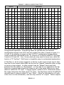
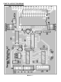
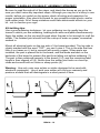
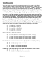
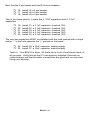
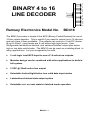
BINARY 4 to 16
LINE DECODER
Ramsey Electronics Model No.
B
D
1
2
4
8
4
1
6
0
1
2
3
4
5
6
7
8
9
10
11
12
13
14
15
BD416
The BD416 provides a simple 4 line BCD (Binary-Coded-Decimal) to one of
16 line output decoder. This is useful if you need to control up to 16 devices
and only have 4 lines available. The outputs can control a 5 volt DC device
@ up to 20mA. Input levels are 5 volt active high logic levels. User
configurable latched/non-latched, and set/reset latched output plus active
high or low data valid strobe. The BD416 can be used as a building block in
many applications. Let your imagination fun wild.
•
5 volt logic level BCD input to one of 16 active low outputs.
•
Modular design can be combined with other applications to build a
full system.
•
5 VDC @ 20mA active low output
•
Selectable Active High/Active Low valid data input strobe
•
Latched/non-latched data output option
•
Selectable set or reset state for latched mode operation
BD416 • 1
PARTIAL LIST OF AVAILABLE KITS:
RAMSEY TRANSMITTER KITS
• FM10C, FM25B FM Stereo Transmitters
• AM1C, AM25 Transmitter
RAMSEY RECEIVER KITS
• FR1C FM Broadcast Receiver
• AR1C Aircraft Band Receiver
• AR2 Aircraft Band Receiver
• SR2C Shortwave Receiver
• AA7C Active Antenna
• SC1C Shortwave Converter
RAMSEY HOBBY KITS
• SG7 Personal Speed Radar
• SS70C Speech Scrambler/Descrambler
• TT1CTelephone Recorder
• MD3C Microwave Motion Detector
• PH14C/15C/16C Peak hold Meters
RAMSEY AUDIO KITS
• SHA1C and SHA2 Headphone Amplifier kits
• UAM4 40 Watt Stereo Amplifier kit
RAMSEY AMATEUR RADIO KITS
• HR Series HF All Mode Receivers
• DDF1 Doppler Direction Finder Kit
• QRP Series HF CW Transmitters
• CW7C CW Keyer
• QRP Power Amplifiers
RAMSEY MINI-KITS
Many other kits are available for hobby, school, scouts and just plain FUN! New
kits are always under development. Write, call or visit www.ramseykits.com for
our free Ramsey catalog.
BD416
Ramsey Electronics publication No. BD416
First Printing: May 2010
COPYRIGHT ©2009 by Ramsey Electronics, LLC. 590 Fishers Station Drive, Victor, New York
14564. All rights reserved. No portion of this publication may be copied or duplicated without the
written permission of Ramsey Electronics, LLC. Printed in the United States of America.
BD416 • 2
Ramsey Publication No. BD416
Manual Price Only $5.00
INSTRUCTION MANUAL FOR
BINARY 4 to 16 LINE
DECODER
TABLE OF CONTENTS
Introduction/Circuit Description....................... 2
Parts Layout Diagram ..................................... 7
Schematic ....................................................... 8
“Learn-As-You-Build” Kit Assembly .............. 10
Parts List ....................................................... 11
Assembly Steps ............................................ 12
Conclusion .................................................... 14
Specifications................................................ 14
Ramsey Kit Warranty .................................... 15
RAMSEY ELECTRONICS, LLC
590 Fishers Station Drive
Victor, New York 14564
Phone (585) 924-4560
Fax (585) 924-4555
www.ramseykits.com
BD416 • 3
Introduction
The BD416 is a simple 4 line binary input to one of 16 lines output interface.
The output can be configured to latch the output when a valid data signal is
applied. The valid data signal may be either an active high or active low logic
level input. In the latched output configuration the output may be set to
initialize to a set, output line “0” low, or reset, output line “15” low, state at
power-up. In non-latched configuration the output initializes to match the
input binary setting on power-up and simply follows the input. The binary
input is active high 5 volt logic level.
BD416 Circuit Operation
If you look on the left side of the schematic you will see the 4 binary input
lines, B0, B1, B2, B3 and “VALID DATA”. The input may be applied to J1, J2
and/or J5. First we’ll discuss the non-latched configuration. A binary code is
applied to B0 thru B3. These 4 lines are applied to U4 pins 3, 6, 10 and 13
respectively. U4 is a quad 2 input multiplexer which means it’s like 4, SPDT
switches. It simply selects one of the input signals on each switch. The
switches are controlled by the “SEL” signal, U4 pin 1. With a high level
applied to U4 pin 1, that’s when no jumper is installed on “LATCH” jumper
H2, the signals applied to the BD416 inputs are directly selected. The
outputs of U4 are pins 4, 7, 9 and 12 and are connected to U3 pins 10,21, 22
and 23 respectively.
U3 is a 4 line to 16 line decoder. It decodes the 4 binary input lines to one of
16 output lines just like it’s name suggests. Only one of the 16 output lines is
low according to the binary code applied to the inputs. This is probably a
good time to explain a little about binary signals.
A binary signal has only two conditions. It can be either a high level, usually
called a “1”, or it can be a low level usually called a “0”. Since we need to be
able to represent 16 conditions and have only two levels to work with we will
need 4 separate binary signal lines. Since most of us are use to the decimal,
or 10’s base counting system we’ll assign each of the 4 binary lines a value.
For the BD416 input B0 will have a value of 1, B1 will equal 2, B2 will be 4
and B3 will equal 8. In order to figure out what the input signal value is in
decimal all you need to do is add the above values of each line that is set to
a 1 together. So if B3 = 0, B2 = 1, B1 = 0 and B1 = 1 the decimal value will
be 0 + 4 + 0 + 1 which equals 5 and output 5 will be low. A binary
representation of this value is written in the order, B3, B2, B1, B0 or “0101”
for this example. For another example the decimal number 9 would be
written as “1001” in binary. Just add 8 + 0 +0 +1 = 9. A table listing all 16
input and output combinations is given in TABLE 1 below.
BD416 • 4
TABLE 1: BD416 INPUT/OUTPUT
INPUT
B B B B
3 2 1 0
0 0 0 0
0
OUTPUT
1 2 3 4 5 6 7 8 9 1
0
1 1 1 1 1 1 1 1 1 1
1
1
1
1
2
1
1
3
1
1
4
1
1
5
1
0
0
0
1
1
0 1 1 1 1 1 1 1 1 1
1
1
1
1
1
0
0
1
0
1
1 0 1 1 1 1 1 1 1 1
1
1
1
1
1
0
0
1
1
1
1 1 0 1 1 1 1 1 1 1
1
1
1
1
1
0
1
0
0
1
1 1 1 0 1 1 1 1 1 1
1
1
1
1
1
0
1
0
1
1
1 1 1 1 0 1 1 1 1 1
1
1
1
1
1
0
1
1
0
1
1 1 1 1 1 0 1 1 1 1
1
1
1
1
1
0
1
1
1
1
1 1 1 1 1 1 0 1 1 1
1
1
1
1
1
1
0
0
0
1
1 1 1 1 1 1 1 0 1 1
1
1
1
1
1
1
0
0
1
1
1 1 1 1 1 1 1 1 0 1
1
1
1
1
1
1
0
1
0
1
1 1 1 1 1 1 1 1 1 0
1
1
1
1
1
1
0
1
1
1
1 1 1 1 1 1 1 1 1 1
0
1
1
1
1
1
1
0
0
1
1 1 1 1 1 1 1 1 1 1
1
0
1
1
1
1
1
0
1
1
1 1 1 1 1 1 1 1 1 1
1
1
0
1
1
1
1
1
0
1
1 1 1 1 1 1 1 1 1 1
1
1
1
0
1
1
1
1
1
1
1 1 1 1 1 1 1 1 1 1
1
1
1
1
0
0
OK, now it gets a little more interesting. We’re going to look at the latched
configuration operation. Everything starts off just like the non-latched
configuration except now U4 is set up to select the other 4 inputs on pins 2, 5,
11 and 14 by placing a jumper on the “LATCH” configuration jumper block.
These inputs are connected to the “Q” outputs of 4 circuits called “D” flip-flops,
2 each in U1 and U5. Yea, I know what you may want to know now, what the
heck is a “D” flip-flop? Well here’s a hopefully easy to understand explanation.
A “flip-flop” is, as it’s name suggests, a device, in this case a logic circuit, that
has one of two output states that can be can be “flipped” between either a high
or low by a logic signal. In other words it can be “flipped” back and forth
between the two states or “flip-flopped”. In the case of our application the flipflops are a special type where the output is set to the same state as an input
which is called the “D” input. A trigger signal, called a clock, determines when
the output assumes the state of the “D” input. The flip-flops used in the BD416
actually have 2 outputs called “Q” and “Qnot”, (“Qnot” is indicated by a Q with
a line over it in the schematic), and we only use the “Q” output. These outputs
BD416 • 5
are always in opposite states. Our flip-flops also have set and reset controls.
When the set control is pulsed low and returned to a high level the “Q” output
is set to a high level. If reset is pulsed low and returned high the “Q” output is
set to a low level. We’ll talk more about these signals later.
The same inputs, B0 thru B3, are connected to the “D inputs, pins 2 and 12 of
U1 and U5, of the 4 “D” flip-flops. The clock, or trigger, inputs of these flipflops, pins 3 and 11 on U1 and U5, are connected to U2 pin 3. U3 is called an
“exclusive or” gate which has 2 inputs. An “OR gate” simply sets it’s output to
a high level if either or both of it’s inputs is high. Since this is a special type of
“OR” gate called an “exclusive OR” it will only set it’s output high when only
one of it’s inputs is high. If both inputs are high it’s output will be set low. This
is very useful because if one of it’s inputs is locked to a high it will set it’s
output to the opposite state of the other input. What’s so great about that you
ask? Well read on and you’ll see what we use it for.
Notice that U2 pin 2 is connected to the “VALID DATA” input and pin 1 is
connected to a high level by R1. Also notice that pin 1 is connected to jumper
H1. By placing a jumper on H2, U2 pin 3 will follow the “VALID DATA” input.
If the jumper is removed pin 3 will be the opposite level of the “VALID DATA”
input. In this way the BD416 can be configured to latch the input data into the
“D” flip-flops on either a low or high level “VALID DATA” signal. By setting up
the data on the input lines B0 – B3 and then triggering that data into the flipflops using the “VALID DATA” input the 16 output lines will be set and latched
to the data value placed on the inputs. It will remain in that state until another
“VALID DATA” signal latches in another input value.
The last operation we need to look at is the “SET” and “RESET” operation of
the flip-flops. “INIZALIZE” jumper H3 is used to determine how the outputs
are set up when power is applied in the latched configuration. When power is
first applied to the BD416 capacitor C6 is discharged and this is a low logic
level and can be applied to either the set, pins 1 and 13, or reset, pins 4 and
10, of U1 and U5 by the placement of the “INITIALIZE” jumper H3. A short
time after power is applied, C6 will rise to a high level and allow the flip-flops
to operate as described above. If “SET” is selected the “Q” outputs of U1 and
U5 will all be set to 0 and output “O” will be set to a low state. If “RESET” is
selected the “Q” outputs of U1 and U5 will all be set to 1 and output “15” will
be set to a low state.
The BD416 requires a power supply level of 5VDC to operate. This power is
applied to either J3 or J6 terminal blocks. If you are using multiple Ramsey
interface modules or other products requiring 5VDC power you may feed the
power thru the DB4-16 module using J3 and J6.
BD416 • 6
PARTS LAYOUT DIAGRAM
BD416 • 7
RAMSEY “LEARN-AS-YOU-BUILD” ASSEMBLY STRATEGY
Be sure to read through all of the steps, and check the boxes as you go to be
sure you didn't miss any important steps. Although you may be in a hurry to see
results, before you switch on the power check all wiring and capacitors for
proper orientation. Also check the board for any possible solder shorts, and/or
cold solder joints. All of these mistakes could have detrimental effects on your
kit - not to mention your ego!
Kit building tips:
Use a good soldering technique - let your soldering iron tip gently heat the
traces to which you are soldering, heating both wires and pads simultaneously.
Apply the solder on the iron and the pad when the pad is hot enough to melt the
solder. The finished joint should look like a drop of water on paper, somewhat
soaked in.
Mount all electrical parts on the top side of the board provided. The top side is
clearly marked with the word “TOP”, you can’t miss it. This is the side that has
little or no traces on it, but is covered with mostly copper. When parts are
installed, the part is placed flat to the board, and the leads are bent on the
backside of the board to prevent the part from falling out before soldering (1).
The part is then soldered securely to the board (2-4), and the remaining lead
length is then clipped off (5). Notice how the solder joint looks on close up,
clean and smooth with no holes or sharp points (6).
Warning: Use only rosin core solder or solder designed to be used with
electronic equipment. Use of acid core solder will void your warranty and
produce a board that will disintegrate in a short period of time.
BD416 • 10
PARTS LIST
Resistors
4-10K ohm (brown-black-orange), R1, R2, R3, R4
Capacitors
2-10uF C6, C7 (10uF, 35V)
5-0.1uF C1, C2, C3, C4, C5 (104)
Connectors
1-20 pin dual row J4
1-10 pin dual row J5
1-3 pin H3
2-2 pin H1, H2
2-3 screw terminal J1, J2
2-2 screw terminal J3, J6
Semiconductors
2-74HC74 dual D flip-flop, U1, U5
1-74HC157 quad 2 input multiplexer, U4
1-74HC154 4 to 16 line decoder, U3
1-74HC86 quad XOR gate, U2
Miscellaneous
3-jumper blocks
1-Printed circuit board
BD416 • 11
ASSEMBLY STEPS
We’ll start with the low profile components and work our way to the tallest.
That will make it easier to install and solder the components. Locate the 5
IC’s, (2x74HC74, 1x74HC154,1x74HC154 1x74HC86). These IC’s may have
letters before and/or after the type depending on the supplier. Be assured
they are the correct part if they have the stated number in the labeling. Notice
that the marking on the board for these IC’s has a small half circle on one end
and that the IC’s have the same type of marking or a small indented dot on
one end. It is important that the IC be installed so it matches the marking on
the board. It may be necessary to gently bend the leads inward on each side
of the IC’s so they are at right angles with the plastic body in order to get them
into the holes in the board. This is easily done by holding the IC so the leads
on one side are flat against a flat surface and then pressing the body so the
leads bend slightly inward. Do this for the leads on both sides of the IC.
Make sure that all the leads go thru the board. When you install the IC it is a
good idea to insert it into the board and slightly bend one lead on opposite
corners on the bottom of the board so it will stay in place. Then make sure all
leads are thru and it is properly oriented before soldering all the leads.
1.
2.
3.
4.
5.
Install U1, a 74HC74
Install U2 a 74HC74.
Install U3, a 74HC154.
Install U4, a 74HC157.
Install U5, a 74HC86.
Next locate the 4, 10K ohm resistors.
6.
7.
8.
9.
Install 10K ohm resistor R1 [brown, black, orange].
Install 10K ohm resistor R2 [brown, black, orange].
Install 10K ohm resistor R3 [brown, black, orange].
Install 10K ohm resistor R4 [brown, black, orange].
Now find the 4 screw terminal connectors, (2, 2position and 2, 3 position).
10.
11.
12.
13.
Install J1 a 3 position connector.
Install J2 a 3 position connector.
Install J3 a 2 position connector.
Install J6 a 2 position connector.
Locate the 10 pin dual row and 20 pin dual row connectors, (one of each)
14. Install J5 a 10 pin dual row connector.
15. Install J4 a 20 pin dual row connector.
BD416 • 12
Next find the 3 pin header and two(2) two pin headers.
16. Install H1 a 2 pin header..
17. Install H2 a 2 pin header.
18. Install H3 a 3 pin header.
This is the home stretch. Locate the 2, 10uF capacitors and 5, 0.1uF
capacitors.
19.
20.
21.
22.
23.
Install C1, a 0.1uF capacitor, (marked 104)
Install C2, a 0.1uF capacitor, (marked 104)
Install C3, a 0.1uF capacitor, (marked 104)
Install C4, a 0.1uF capacitor, (marked 104)
Install C5, a 0.1uF capacitor, (marked 104)
The next two capacitors MUST be installed with the lead marked with a stripe
and/or “-“ in the hole opposite the “+” printed on the board.
24. Install C6, a 10uF capacitor, watch polarity.
25. Install C7, a 10uF capacitor, watch polarity.
That’s it. Your BD416 is done. All that’s left is to do a final visual check of
all our work. Verify that all the IC’s are properly installed, there are no
solder bridges and that all solder connections are good and you can start
using your decoder.
BD416 • 13
If you enjoyed this Ramsey product, there are plenty more to choose from in
our catalog - visit our website at http://www.ramseyelectronics.com or call today!
CONCLUSION
We sincerely hope that you will enjoy the use of this Ramsey product. As always, we have tried to compose our manual in the easiest, most “user
friendly” format possible. As our customers, we value your opinions, comments, and additions that you would like to see in future publications. Please
submit comments or ideas to:
Ramsey Electronics, LLC.
Attn. Hobby Kit Department
590 Fishers Station Drive
Victor, NY 14564
or email us at: [email protected]
And once again, thanks from the folks at Ramsey!
BD416 SPECIFICATIONS
Input Requirements:
Power:
Logic:
5VDC
4 BCD lines, 5V active high
Output Configuration:
Open collector, active low, 1 of 16 lines
Output:
5VDC max @ 20mA max
Dimensions:
Board:
Mounting:
Weight:
2.5”(W) X 3.82” (L)
63.5mm (W) X97mm (L)
4 holes, 4/40 screw clearance on 2” x 3” pattern
4 holes on 50.8mm x 76.3mm pattern
0.7 Oz, 0.0198 Kg
BD416 • 14
THE RAMSEY KIT WARRANTY
1. GENERAL:
Notice that this is not a "fine print" warranty. We want you to understand your rights and ours too! All Ramsey kits will work if
assembled properly. The very fact that your kit includes this new manual is your assurance that prior to release of this kit, a
varied group of knowledgeable people have assembled this kit from scratch using this manual. During this process, changes
and additions are noted by each assembler and integrated into the final version of the manual…which you have! If you need
help, please read through your manual carefully, all information required to properly build and test your kit is contained within
the pages! However, customer satisfaction is our goal, so in the event that you do have a problem, please note the following:
2. DEFECTIVE PARTS:
It's always easy to blame a part for a problem in your kit. Before you conclude that a part may be bad, thoroughly check your
work. Today's semiconductors and passive components have reached incredibly high reliability levels, and it’s sad to say that
our human construction skills have not! But on rare occasions a sour component can slip through. All of our kit parts carry the
Ramsey Electronics Warranty that they are free from defects for a full ninety (90) days from the date of purchase. Defective
parts will be replaced promptly at our expense. If you suspect any part to be defective, please mail it to our factory for testing
and replacement. Please send only the defective part(s), not the entire kit. The part(s) MUST be returned to us in suitable
condition for testing. Please be aware that testing can usually determine if the part was truly defective or damaged by assembly
or usage. Don't be afraid of telling us that you “damaged it” or “burned it out”, we're all human and in most cases, replacement
parts are very reasonably priced. Remember, our goal for over three decades is to have a happy customer, and we’re here to
work WITH you, not AGAINST you!
3. MISSING PARTS:
Before assuming a part value is missing, check the parts listing carefully to see if it is a critical value such as a specific coil or
IC, or whether a RANGE of values is suitable for the component (such as a "100 to 500 uF capacitor"). Often times, common
sense will solve a mysterious missing part problem. If you're missing five 10K ohm resistors and received five extra 1K
resistors, you can pretty much be assured that the “1K ohm” resistors are actually the “missing” 10 K parts ("Hum-m-m, I guess
the orange band really does look red!") Ramsey Electronics project kits are packed with pride in the USA by our own staff
personnel. While separate QC checks are made on all product kits, we too are human, and once in a great while there is a
chance something can get through those checks! If you believe we packed an incorrect part or omitted a part clearly indicated
in your assembly manual for your Ramsey kit, please contact us with information on the part you need. Contact our Repair
Department via telephone, email or writing. Please have your invoice number and date of purchase handy.
4. REFUNDS:
All Ramsey products, kit or factory assembled units have an unconditional 10 day (from the date of purchase) return policy to
examine our products. If you are not satisfied for any reason, you may return your unassembled kit with all the parts and
instructions, or your factory assembled and tested product, together with your proof of purchase to the factory for a full refund
less shipping. The return package should be packed securely. Insurance and tracking is highly recommended. A reminder, this
applies to unassembled kits. They must be in the same new condition as received, not partially assembled! Assembled kits
cannot be returned for credit. No RMA’s are required; simply return to Ramsey Electronics LLC, Attn: Product Returns, 590
Fishers Station Drive, Victor, NY, 14564. If you have any questions, please contact us at 585-924-4560.
5. FACTORY REPAIR OF ASSEMBLED KITS:
Most of us at Ramsey are technically oriented and we do realize that things happen! Even following the best practices, with all
of the best intentions, there is that chance that your kit doesn’t work when you have completed it. Each manual goes into
detailed troubleshooting based on the specific kit to help you troubleshoot the problem. We have found that 95% of returned
kits involved wrongly installed components (wrong part or backwards polarity). This section of the warranty assumes you have
gone through all those steps, and have now reached the point that you need to send it back.
To qualify for factory repair of customer assembled kits, the following conditions apply:
1. Kits must not be assembled with acid solder flux
2. Kit boards or circuits must not be modified in any manner from the version received
3. Kits must be fully assembled, not partially assembled. Our warranty does not include “finishing” your kit!
4. Must include a full description of the problem encountered including the troubleshooting steps you have already done.
5. Must not include non-standard, non-Ramsey accessories, cases, enclosures, knobs, etc. or any batteries.
6. Must include the minimum repair fee of $25 USD in the form of check, money order or credit card authorization.
7. Ramsey Electronics, LLC reserves the right to refuse any repair due to excessive errors in construction methods.
8. If, due to customer construction methods, the repair is estimated to exceed the minimum flat rate, Ramsey Electronics,
LLC will contact the customer to discuss the repairs needed and to receive authorization and payment for repair prior
to repair.
9. In the unlikely case that a defective part is found to be the cause of the problem, the repairs will be made at no-charge
to the customer, and any payments received for repair will be returned or credited back to the customer.
10. Properly pack your kit, insure the package, and use a carrier that can be tracked. Ramsey Electronics, LLC is not
responsible for any loss or damage in shipment. Send the package together with your repair fee to the return address
below. No RMA is required.
6. FACTORY REPAIR FEES:
Please understand that our Tech Support Group personnel are not volunteers! They are a dedicated group of highly trained
technicians each configured with a very properly equipped test bench. Upon receipt of a repair, the setup, testing, diagnosis,
repair, paperwork, and repacking of your kit requires nearly an hour of their time regardless of the size or complexity of the kit!
The minimum repair fee represents ½ hour Tech Support time at $50/hour USD. We try to keep all kit repairs within the realm
of the $25 flat rate whenever possible…and trust us; we exceed that time spent on most kits received more often than not!
7. CONTACT INFORMATION AND RETURN ADDRESS:
Technical Questions
RAMSEY ELECTRONICS, LLC
Attn: Tech Support
BD416
590 Fishers Station Drive
Victor, NY 14564
585-924-4560; 585-924-4886 Fax
[email protected]
Product Repair & Returns
• 15
RAMSEY ELECTRONICS, LLC
Attn: Repairs
590 Fishers Station Drive
Victor, NY 14564
585-924-4560; 585-924-4886 Fax
[email protected]
Quick Reference
Introduction/Circuit Description .......................2
Parts Layout Diagram .....................................7
Schematic........................................................8
Parts List ...................................................... 11
Assembly Steps............................................ 12
Specifications ............................................... 14
REQUIRED TOOLS
• Soldering Iron
• Thin Rosin Core Solder
• Needle Nose Pliers
• Small Diagonal Cutters
ADDITIONAL SUGGESTED ITEMS
Helping Hands Holder for PC Board/
Parts
• Desoldering Braid
•
RAMSEY ELECTRONICS, LLC
590 Fishers Station Drive
Victor, New York 14564
Phone
(585) 924-4560
Fax
(585) 924-4555
www.ramseykits.com
Ramsey Publication No. BD416
Assembly and Instruction manual for:
BINARY 4 to 16 LINE DECODER
BD416 • 16