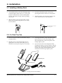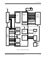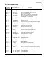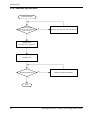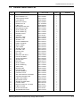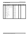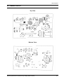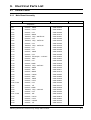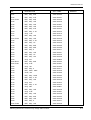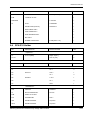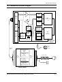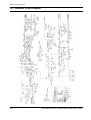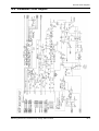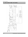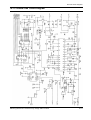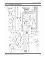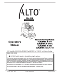
1
CDMA PORTABLE
CELLULAR TELEPHONE
SCH-211
SERVICE
CDMA PORTABLE CELLULAR TELEPHONE
Manual
CONTENTS
1. General Introduction
2. Specification
3. Installation
4. NAM Programming
5. Circuit Description
CDMA
SEND
1
END
2
ABC
3
4
GHI
5
JKL
6
MNO
7
PQRS
8
TUV
9
WXYZ
0
OPER
PWR
CLR
OK
6. Troubleshooting
DEF
MENU
7. Exploded Views and Parts List
8. PCB Diagrams
9. Electrical Parts List
10. Block & Circuit Diagrams
ELECTRONICS
Samsung Electronics Co.,Ltd.
GH68-00335A
Specification
1
Samsung Electronics - Contents may change without notice.
1. General Introduction
The SCH-211 cellular phone functions as both analog cellular phone working in AMPS (Advanced Mobile
Phone Service) mode and digital cellular phone working in CDMA (Code Division Multiple Access) mode.
CDMA type digital mode applies DSSS (Direct Sequential Spread spectrum) mode which first came to be
used in the military.
The DSSS reduces channel cross talk and allow to use one frequency channel by multiple users in the same
specific area, resulting in increase of channel capacity to about ten times compared to that of analog mode
currently used.
Soft/Softer Handoff, Hard Handoff, and Dynamic RF Power Control technologies are combined into this
phone to reduce the call drop while usage.
CDMA digital cellular network consists of MSO (Mobile Switching Office), BSC (Base Station Controller), BTS
(Base Station Transmission System), and MS (Mobile Station). MS meets the specifications of the below:
¥ UIS-95A : Mobile Station-Base Station Compatibility Standard for Dual-Mode Wideband Spread Spectrum
Cellular System
¥ UIS-96A : Speech Service Option 1 Standard for Dual-Mode Wideband Spread Spectrum Cellular Systems
¥ UIS-98A : Standards for Dual-Mode Wideband Spread Spectrum Cellular Mobile Station
¥ UIS-126 : Mobile Station Loopback Service Options Standard
SCH-211 is composed of main handset, rapid charger, cradle, two batteries (1300 mAh, 850 mAh), hands-free
kit, and travel charger. Hands-Free Kit is designed to be operated in half-duplex mode taking turn-around
delay between the phone and the system into account.
Samsung Electronics-Contents may change without notice.
1-1
General Introduction
MEMO
1-2
Samsung Electronics - Contents may change without notice.
2.
Specification
2-1 General
Frequency Range
Transmitter
Receiver
Digital Mode
: 824.64 ~ 848.37 MHz
: 869.64 ~ 893.37 MHz
Analog Mode
824.04 ~ 848.97 MHz
869.04 ~ 893.97 MHz
Channel Spacing
: 1.23 MHz
30 kHz
Number of Channels
: 20 FA
832 CHs
Duplex Spacing
: 45 MHz
Frequency Stability
: ± 2.5 ppm (– 30 °C ~ + 60 °C : -22 °F ~ 140 °F)
Operating Temperature
: – 20 °C ~ + 50 °C (–4 °F ~ 122 °F)
Operating Voltage
HHP
Hands-free
: 7.2V DC (± 10 %)
: 13.7V DC (± 10 %)
Size and Weight
including standard battery
including extended-life battery
: 130 ✕ 51 ✕ 27.5 mm, 205 g (5.12 ✕ 2 ✕ 0.94 inch, 7.2 oz)
: 130 ✕ 51 ✕ 37 mm, 207 g (5.12 ✕ 2 ✕ 1.46 inch, 7.4 oz)
Operating Time
Digital mode
Standby Time
Talk Time
Analog
Standby Time
Talk Time
:
:
:
:
:
:
:
:
about
about
about
about
about
about
about
about
50 ~ 55 hours
85 ~ 90 hours
150 min (with
250 min (with
10 ~ 12 hours
16 ~ 18 hours
100 min (with
170 min (with
(with standard battery)
(with extended-life battery)
standard battery)
extended-life battery)
(with standard battery)
(with extended-life battery)
standard battery)
extended-life battery)
2-2 Analog Mode
TRANSMITTER
RF output power
: 0.6 W (+2/–4 dB)
Carrier ON/OFF Conditions
“ON” Condition
“OFF” Condition
: within ± 3 dB of specification output (in 2mS)
: below – 60 dBm (in 2mS)
Compressor
Compression Rate
Attack Time
Recovery Time
Reference Input
:
:
:
:
2:1
3 mS
13.5 mS
Input level for producing a nominal ± 2.9 kHz peak frequency
deviation of transmitted carrier
Samsung Electronics-Contents may change without notice.
2-1
Specification
Preamphasis
: 6 dB/OCT within 0.3 ~ 3 kHz
Maximum Frequency Deviation
F3 of G3
Supervisory Audio Tone
Signaling Tone
Wideband Data
:
:
:
:
± 12 kHz
± 2 kHz
± 8 kHz
± 8 kHz
Post Deviation Limiter Filter
3.0 kHz ~ 5.9 kHz
5.9 kHz ~ 6.1 kHz
6.1 kHz ~ 15 kHz
Over 15 kHz
:
:
:
:
above
above
above
above
(± 10 %)
(± 10 %)
(± 10 %)
(± 10 %)
40LOG (F/3000) dB
35 dB
40LOG (F/3000) dB
28 dB
Spectrum Noise Suppression
For All Modulation
f0 + 20 kHz ~ f0 +45 kHz
: above 26 dB
For Modulation by Voice and SAT
f0 +45 kHz
: above 63 +10LOG (Py) dB
For Modulation by WBD (without SAT) and ST (with SAT)
f0 +45 kHz ~ f0 +60 kHz
: above 45 dB
: above 65 dB
f0 +60 kHz ~ f0 +90 kHz
f0 +90 kHz ~ 2f0
: above 63 +10LOG (Py) dB
(where f0= carrier frequency
Py= mean output power in watts)
Harmonic and Conducted Spurious Emissions
: above 43 +10LOG (Py) dB
RECEIVER
DE-Emphasis
: – 6 dB/OCT within 0.3 ~ 3 kHz
Expander
Expansion Rate
Attack Time
Recovery Time
Reference Input
:
:
:
:
Sensitivity
: 12 dB SINAD/–116 dBm
Intermodulation Spurious Response Attenuation
: above 65 dB
RSSI Range
: above 60 dB
1:2
within 3 ms
within 13.5 ms
Output level to a 1000 Hz tone from a carrier within ±2.9
kHz peak frequency deviation
Protection Against Spurious Response Interference : above 60 dB
In Band Conducted Spurious Emissions
Transmit Band
Receive Band
: below – 60 dBm
: below – 80 dBm
Out of Band Conducted Spurious Emissions
: below – 47 dBm
2-2
Samsung Electronics - Contents may change without notice.
Specification
Radiated Spurious Emissions
Frequency Range
Maximum Allowable EIRP
25 ~ 70 MHz
70 ~ 130 MHz
130 ~ 174 MHz
174 ~ 260 MHz
260 ~ 470 MHz
470 ~ 1 GHz
– 45 dBm
– 41 dBm
– 41 ~ – 32 dBm
– 32 dBm
– 32 ~ – 26 dBm
– 21 dBm
2-3 Digital Mode
Waveform Quality
: above 0.944
Time Reference
: within ± 1uS
RX Sensitivity
: – 104 dBm, FER = within 0.5%
Dynamic Range
: – 104 dBm ~ – 25 dBm, FER = within 0.5%
TX Output Power
: Maximum 320 mW (25dBm)
TX Frequency Deviation
: within ± 300 Hz
Occupied Band Width
: 1.32 MHz
TX Conducted Spurious Emissions
: 900 kHz
: 1.98 MHz
Minimum TX Power Control
: below – 50 dBm
Open Loop Power Control
: – 25 dBm
– 57.0 dBm ~ – 38.5 dBm
– 65 dBm
– 17.5 dBm ~ + 1.5 dBm
– 104 dBm + 18.0 dBm ~ + 30.0 dBm
Standby Output Power
: below – 61 dBm
Closed Loop TX Power Control Range
: Test 1
Test 2
Test 3
Test 4
Test 5
below – 42 dBc / 30 kHz
below – 54 dBc / 30 kHz
beyond ± 24 dB
0 mS ~ 2.5 mS
beyond ± 24 dB
beyond ± 24 dB
beyond ± 24 dB
Samsung Electronics-Contents may change without notice.
2-3
Specification
MSC Transmitter Frequency
FA NO.
CH. NO.
CENTER FREQUENCY
FA NO.
CH. NO.
CENTER FREQUENCY
1
1011
2
29
824.640MHz
11
404
837.120MHz
825.870MHz
12
445
838.350MHz
3
70
827.100MHz
13
486
839.580MHz
4
111
828.330MHz
14
527
840.810MHz
5
152
829.560MHz
15
568
842.040MHz
6
193
830.790MHz
16
609
843.270MHz
7
234
832.020MHz
17
650
844.270MHz
8
275
833.250MHz
18
697
845.910MHz
9
316
834.480MHz
19
738
847.140MHz
10
363
835.890MHz
20
779
848.370MHz
MSC Receiver Frequency
2-4
FA NO.
CH. NO.
CENTER FREQUENCY
FA NO.
CH. NO.
CENTER FREQUENCY
1
1011
869.640MHz
11
404
882.120MHz
2
29
870.870MHz
12
445
883.350MHz
3
70
872.100MHz
13
486
884.580MHz
4
111
873.330MHz
14
527
885.810MHz
5
152
874.560MHz
15
568
887.040MHz
6
193
875.790MHz
16
609
888.270MHz
7
234
877.020MHz
17
650
889.270MHz
8
275
878.250MHz
18
697
890.910MHz
9
316
879.480MHz
19
738
892.140MHz
10
363
880.890MHz
20
779
893.370MHz
Samsung Electronics - Contents may change without notice.
Specification
2-4 CDMA Debug Display Information (menu 8)
IN IDLE MODE
➀ Sxxxxx : SID (System ldentification) toggle
➀
➁
Nxxxxx : NID (Network Identification) toggle
➂
➁ Slx : Slot cycle index (lowest between the system
and the phone will be used)
SIDxxxxx SIx
➃
x
T– xx
Rxxx – xx
Pxxx
CHxxxx
➆
➂ Handset Status : 0 - Acquisition
➅
➇
➄
1
2
3
4
5
- Synchronization
- Paging (Idle)
- Traffic Initialization
- Traffic Mode
- Exit
➃ T-xx : Tx adjust, Value ranges from +63 ~-63dB
➄ Dxxx or Rxxx : sector power in dBm
IN CONVERSATION MODE
➈
SVx RVx
T – xx
Pxxx
⑩
➅ -xx : ec/Io
11
➆ Pxxx : PN offset or Pilot #
xx
➂
x
➇ CHxxxx : channel number
Rxxx – xx
➈ TV : Tx vocoder rate (8 is full rate, 1 is 1/8th rate)
CHxxxx
⑩ RV : Rx vocoder rate (8 is full rate, 1 is 1/8th rate)
11
xx : Walsh code used in traffic channel
2-5 FM Debug Display Information (menu 8)
➀ SIDxxxxx : FM Home System ID
➀
➁ PWRx : Power Level 0~7
➂
➂ SATx : Supervisory Audio Tone code (0~3)
SIDxxxxx
➁
PWR x
SATx
➃ x (Using Frequency Band) : A Band or B Band
x
RSSIxxx
➄
➄ RSSIxxx : RSSI value
CHxxxx
➅ CHxxx : Using Channel
➂
➅
Samsung Electronics-Contents may change without notice.
2-5
Specification
MEMO
2-6
Samsung Electronics - Contents may change without notice.
3. Installation
3-1 Installing a Battery Pack
1.
2.
To attach the battery pack after charging, align
it with the phone about 1cm (1/2Ó) away from
its place so that the two arrows on the phone
are seen, the battery charge contacts pointing
downward.
3.
To remove the battery pack, release it by
pressing the button on the rear of the phone.
4.
Slide the battery pack downward about 1cm
(1/2Ó) and lift it away from the phone.
Slide the battery pack upwards until it clicks
firmly into position. The phone is now ready
to be turned on.
Press this button to release
the battery pack
3-2 For Desk Top Use
1.
Choose a proper location to install the charger
for desk top use.
2.
Plug the power cord of the charger into an
appropriate wall socket. When the power is
connected correctly, the lamps turn on briefly.
3.
To charge the battery pack, insert the battery
pack into the rear slot of the charger. The
lamp marked BAT on the front panel of the
charger lights up red.
4.
If you do not wish to use the phone while
charging the battery, insert the phone with the
battery pack attached into the front slot of the
charger. The lamp marked PHONE on the
front panel of the charger lights up red.
SA
MS
UN
G
Extended Battery Pack
SCH-211 MAIN
Standard Battery Pack
Figure 3-1 Charging the Phone and Battery
Samsung Electronics-Contents may change without notice.
3-1
Installation
Item
Model Name
Desk Top Rapid Charger
DTC58
GH44-40034A
Standard Battery Pack
BTL850SB
GH43-10104A
Extended Battery Pack
BTL1350EB
GH43-10103A
Service Part#
SPECIFICATIONS USING ”DTC 58”
Charging time
Stand by time (hours)
Talking time (min)
(hours)
Digital
Analog
Digital
Analog
Standard Battery Pack (Li-ion: 800mAh)
2~3
50 ~ 55
10 ~ 12
150
100
Extendard Battery Pack (Li-ion: 1350mAh)
2.5 ~ 3.5
85 ~ 90
16 ~ 18
250
170
Product
3-3 For Mobile Mount
3-3-1 Antenna
1.
3-2
Choose a proper location to install the
antenna.
¥ UThe center of the roof top provides the
best performance.
¥ UThe edge of the rear trunk also provides a
good performance. However, the antenna
should be higher than the roof of the car.
¥ UIn case of on-glass antenna, you should
align the antenna base with the round plate
to connect the cables correctly.
2.
Mount the antenna vertically, connect the
antenna cable.
3.
Tighten the antenna nut fully.
Samsung Electronics - Contents may change without notice.
Installation
3-3-2 Cradle
1.
Choose a location where it is easy to reach
and does not interfere with the driverÕs safe
operation of the car.
4.
Place the cradle onto the remaining half of the
clamshell and assemble them by using the
screws.
2.
Separate the two halves of the clamshell by
removing the two large slotted screws. See the
figure 3-2.
5.
Reassemble the two halves of the clamshell
together. Adjust the mounting angle and
tighten the two slotted screws.
3.
Drill holes and mount the lower half of the
clamshell by using the screws.
Cradle
To Antenna
To Cellular
Telephone
To Hands-free Box
Vehicle
32
m
m
m
m
32
Figure 3-2 Cradle Installation
Samsung Electronics-Contents may change without notice.
3-3
Installation
3-3-3 Hands-Free Box
3-3-4 Hands-Free Microphone
1. Drill holes in a proper location for the handsfree box, attach the mounting bracket by using the
screws. See the figure 3-3.
1.
It is recommended to install the microphone
where it is 30-45 cm (12-18Ó) away from the
driver. Choose the location where is least
susceptible to interference caused by external
noise sources, ie, adjacent windows, radio
speakers, etc. Normal place is the sun visor.
2.
Once the microphone has been correctly
positioned, connect the microphone wire to
the MIC jack on the hands-free box.
2.
Install the hands-free box into the bracket.
Mounting Bracket
40
m
m
m
m
56
Figure 3-3 Hands-Free Box Installation
3-4
Samsung Electronics - Contents may change without notice.
Installation
3-3-5 Cables
1.
Connect the cradle and the hands-free box
with the data cable. See the figure 3-4.
2.
Connect the antenna cable to the RF jack of
the cradle.
3.
Connect the power cable as follows:
Connect the red wire to the battery (+) terminal, black wire to the battery (-) terminal.
Then connect the orange wire to the switched
side of the ignition switch, and then connect
the brown wire to the stereo mute wire from
your vehicle stereo.
4.
Connect the other end of the power cable to
the PWR jack of the hands-free box.
Notes:
¥ It is recommended to connect the power cable
directly to the battery to avoid power noise.
¥ Make sure the connection, in the vehicle,
between the battery (-) terminal and vehicle
chassis is made correctly.
¥ Make sure the fuse having a proper capacity is
used on the power cable.
¥ Make sure the cables do not pass over any sharp
metal edge that may damage it.
SA
MS
UN
G
PWR
3A FUSE
RED
BLACK
ORANGE
BROWN
BAT.(+)
BAT.(-)
IGN. Switch
STEREO Mute
Figure 3-4 Cable Connections
Samsung Electronics-Contents may change without notice.
3-5
Installation
MEMO
3-6
Samsung Electronics - Contents may change without notice.
4. NAM Programming
4-1 Quick NAM Programming
Key in
Function
Select Quick NAM Programming
Enter Lock
654321
Envice Service Lock Code.
NAM Program
1:Setup NAM1
2:Setup NAM2
1
Choose ÒNAM1Ó
phone #
1234567890
Phone Number
OK
Phone Number.
Mobile ID #
1234567890
Mobile ID Number
OK
Mobile ID Number.
Anlg HomeSID
20
Number
OK
Analog System ID Number.
Dgtl HomeSID
20
Number
OK
Digital System ID Number.
Prog. More?
No
Exit or Enter Long NAM
➞
Menu, 4, 0
➞
LCD Display
✻ or #
OK
Samsung Electronics-Contents may change without notice.
4-1
NAM Programming
4-2 General Setup
LCD Display
Key in
Function
NAM Program
1:General
2:Setup NAM1
1
-choose ÔGENERAL.Õ
General
ESN
B0000000
Volume ▲
Electronic Serial Number of the phone.
General
CAIversion
Volume ▲
The version of the Common Air Interface supported by the mobile.
3
➞
➞
General
VOC select
SO_VOICE_13K
✻ or #
OK
Vocoder data rate.
General
SCM
01101010
Volume ▲
Station Class Mark displays the power class (bit 0~1),
transmission (bit2), slotted (bit5), dual mode (bit6).
General
Service code
654321
Number
OK
Six-digit number supplied by the user which enables service
lock.
Lock
4-digit code
OK
Four-digit number supplied by the user which enables
electronic locking of the phone.
Slot Mode
Yes
➞
➞
Code
0000
✻ or #
OK
Slot Index
4-2
➞
Pref NAM(1~4)...
Digital pref
Slot mode index.
Specifies the duration and frequency of times that the mobile
checks the paging channel. The higher the value, the less often the
mobile looks at the paging channel, and the more power is saved.
0-7
OK
➞
2
Enables slot mode.
✻ or #
OK
Preferred system selection for NAM(1~4).
Up to four NAMs are allowed for the phone. This lists one of the
four NAMs and allows you to program both the FM and CDMA
settings.
Samsung Electronics - Contents may change without notice.
NAM Programming
4-3 Setting up Long NAM1
Key in
Function
2
-choose ÔSetup NAM1.Õ
NAM1 Digital
IMSI_MCC
000
Number
OK
International Mobile Station Identity Mobile Country Code.
NAM1 Digital
IMSI_MNC
00
Number
OK
International Mobile Station Identity Mobile Network Code.
NAM1 Digital
phone #
3003003000
Phone Number
OK
Phone number.
NAM1 Digital
Mobile ID #
3003003000
Mobile ID Number
OK
Mobile ID Number.
NAM1 Digital
Home SID
#(1~4)
1700
Number
OK
SID(1~4) written in the list, current status is displayed.
to change, enter new one stores it.
NAM1 Digital
Home NID
#(1~4)
1700
Number
OK
NID(1~4) written in the list, current status is displayed.
to change, enter new one stores it.
NAM1 Digital
Pchn Sys A
700
Channel Number
OK
Primary CDMA channel for the A carrier.
Ranges from 0 to 1,023.
0 indicates no channel.
NAM1 Digital
Pchn Sys B
700
Channel Number
OK
Primary CDMA channel for the B carrier.
Ranges from 0 to 1,023.
0 indicates no channel.
NAM1 Digital
Schn Sys A
700
Channel Number
OK
Secondary CDMA channel for the A carrier.
Suggested setting is 0:ranges form 0 to 1,023.
NAM1 Digital
Schn Sys B
700
Channel Number
OK
Secondary CDMA channel for the B carrier.
Suggested setting is 0:ranges form 0 to 1,023.
NAM1 Digital
Home SID Reg
Yes
✻ or #
OK
➞
NAM Program
1:General
2:Setup NAM1
➞
LCD Display
CDMA Home System ID.
Enables the phone to allow mobile terminated calls while in
the home system. Controls the types of registration allowed
for the phone.
Samsung Electronics-Contents may change without notice.
4-3
NAM Programming
NAM1 Digital
Forn NID Reg
Yes
➞
NAM1 Digital
Forn SID Reg
Yes
➞
Key in
➞
LCD Display
✻ or #
OK
➞
✻ or #
OK
ID Number
OK
NAM1 Digital
Lockout SID1
0
Function
CDMA foreign SID, current status is displayed.
Changes the status.
Stores it.
CDMA foreign NID, current status is displayed.
changes the system.
stores it.
CDMA Lock System ID.
Enable you to specify up to six SIDs that the phone will be
prohibited from acquiring in CDMA mode. If all six SIDs are
set to zero, no lock restrictions will be in effect and the phone
can acquire all SIDs.
Default setting is 0:ranges from 0 to 32,767 up to six SIDs.
Class Number
OK
CDMA Access Overload Class.
This two-digit number specifies the level of priority assigned
to the mobile for accessing the system.
Ranges from 0 to 15.
NAM1 Analog
Phone #
3003003000
Phone Number
OK
Phone number.
NAM1 Analog
Home SID
4369
IDNumber
OK
FM Home System ID.
The Identification of the cellular system in which the mobile
station subscribes for service.
Cellular Service Provider.
NAM1 Analog
1st Page Chn
333
Channel Number
OK
NAM1 Digital
ACCOLC
➞
NAM1 Analog
ACCOLC
✻ or #
OK
➞
✻ or #
OK
0
4-4
➞
NAM1 Analog
Auto Reg
Yes
➞
0
1st Paging Channel.
Suggested setting is 333 for the A carrier, 334 for the B carrier:
ranges from 313 to 333 for A and 334 to 354 for B.
Primary analog paging channel: setting depends on whether
the service is provided by the A carrier or the B carrier.
Enables autonomous registration.
FM Access Overload Class.
This two-digit number specifies the level of proirity assigned
to the mobile for accessing the system.
Ranges from 0 to 15.
Samsung Electronics - Contents may change without notice.
5. Circuit Description
5-1 Logic Section
5-1-1 Power Supply
With the battery installed on the phone and by
pressing the PWR key, the VBATT and ON_SW
signals will be connected. This will turn on Q102
(2SC4081BR) and will drive DC-DC converter
(U123) to output 5.0V. This in turn will be supplied to pin 6 of regulators (U121 and U122), thus
releasing them from the shut-down state to output
regulated 3.3V.
The VBATT applied to ON_SW will turn on Q103
(DTC144EE) resulting in the signal
ON_SW_SENSE to change state from HIGH to
LOW. This will allow MSM to send out PS_HOLD
(logical HIGH) to turn on Q102 even after the
PWR key is released.
The voltage (+3.3V) from U121 is used in the digital parts of MSM and BBA. The voltage (+3.3AV)
from U122 is used in the analog part of BBA. The
voltage from U124 (output of 5V) is used for the
audio circuitry.
CPU
INTEL 80186 CMOS type 16-bit microprocessor is
used for the main processing. The CPU controls
all the circuitry. For the CPU clock, 27MHz
resonator is used.
FLASH ROM
One 8 MBIT FROM is used to store the terminalÕs
program. Using the down-loading program, the
program can be changed even after the terminal is
fully assembled.
SRAM
One 2 MBIT SRAM is used to store the internal
flag information, call processing data, and timer
data.
EEPROM
5-1-2 Logic Part
The Logic part consists of internal CPU of MSM,
RAM, ROM and EEPROM. The MSM receives
TCXO and CHIPX8 clock signals from the BBA
and controls the phone during the CDMA and the
FM mode. The major components are as follows:
¥ CPU : INTEL 80186 core
¥ FROM
: U126 (MBM29LV800T) - 8MBIT
FLASH ROM
¥ SRAM
: U127 (KM68V2000I) - 2MBIT
STATIC RAM
¥ EEPROM
: U113 (AT24C128) - 128KBIT SERIAL EEPROM
One 128 KBIT EEPROM is used to store ESN,
NAM, power level, volume level, and telephone
number.
KEYPAD
For key recognition, key matrix is setup using
SCAN0-6 of STORE signals and KEY0-3 of input
ports of MSM. Eight LEDs and backlight circuitry
are included in the keypad for easy operation in
the dark.
LCD MODULE
LCD module contains a controller which will
display the information onto the LCD by 8-bit
data from the MSM. It also consists a DC-DC
converter to supply -3.5V for fine view angle and
LCD reflector to improve the display efficiency.
Samsung Electronics-Contents may change without notice.
5-1
Circuit Description
5-1-3 Baseband Part
MOBILE SYSTEM MODEM (MSM)
The MSM equipped with the INTEL 80186 CPU
core is an important component of the CDMA
cellular phone. The MSM comes in a 176 pins
TQFP package. The interface block diagram is
shown on page 6-3.
ADC Interface
MICROPROCESSOR INTERFACE
Data Port Interface
The interface circuitry consists of reset circuit,
address bus (A0-A19), data bus (AD0-AD15), and
memory controls (ALE, DT_R, HWR/, LWR/,
RAM_CS/, ROM_CS).
Includes the UART. Also, supports Diagnostic
Monitor (DM) and HP equipment interface.
INPUT CLOCK
The MSM outputs 2.048 MHz PCM_CLK (pin 19)
and 8 KHz CODEC_SYNC (pins 16,20) to the
CODEC (U117). The voice PCM data from the
MSM (U101) PCM_DIN (pin135) is compressed
into 8KHz by QCELP algorithm in the CDMA
mode. In FM mode, the data is processed by
D_FM.
¦UCPU clock: 27 MHz
¦UTXCO/4 (pin 34): 4.92 MHz. This clock signal
from the BBA is the reference clock for the MSM
except in CDMA mode.
¦UCHIPX8 : 9.8304 MHz. The reference clock
used during the CDMA mode.
CODEC Interface
RF Interface
TX : TX_AGC_ADJ (pin 35) port is used to control
the TX power level and PA_ON (pin 44) signal is
used to control the power amplifier.
BBA INTERFACE
CDMA, FM Data Interface
¥ TXIQDATA0-7 (pins 24-32) : TX data bus used
during both CDMA and FM mode.
¥ C_RX_IDATA0-3 (pins 16-20) and
C_RX_QDATA0-3 (pins 12-15) : RX data bus
used during CDMA mode.
¥ FM_RX_IDATA (pin 7) and FM_RX_QDATA
(pin 8) : RX data bus used during FM mode.
Clock
RX : AGC_REF (pin 36) port is used to control the
RX gain and TRK_LO_ADJ (pin 45) is used to
compensate the TCXO clock.
General Purpose I/O Register Pins
Input/output ports to control external devices.
Power Down Control
¥ TX_CLK (pin 22), TX_CLK/(pin 23) : Analog to
Digital Converter (ADC) reference clock used in
TX mode.
¥ CHIPX8 : ADC reference clock used in CDMA
RX mode.
¥ FMCLK : Reference clock in FM RX mode.
5-2
ADC_CLK (pin 3), ADC_ENABLE (pin 1) and
ADC_DATA (pin 2) are required to control the
internal ADC in the BBA.
When the IDLE/ signal turns LOW, only the TX
sections will be disabled. If both the IDLE/ and
SLEEP/ changes to LOW, all the pins except for
the TXCO is disabled.
Samsung Electronics - Contents may change without notice.
Circuit Description
ANTENNA
RF
UNIT
XTAL
PA_ON
SYNTH_LOCK
TRK_LO_ADJ
TX_AGC_ADJ
RX_AGC_ADJ
RF
INTERFACE
80186
MICROPROCESSOR
CORE
RESIN/
RESOUT
LWR/
HWR/
RD/
DT_R/
EXTERNAL
RAM, ROM,
EEPROM,
DISPLAY &
OTHER
PERIPHERALS
PCS6/
RAM_CS/
ROM_CS/
EEPROM_CS/
AD0~AD15
A0~A19
MSM2300
IDLE/
SLEEP/
FM/
FIFOED SERIAL
DATA PORT
DP_TX_DATA
DP_RX_DATA
MODE
CONTROL
SUPPORT
KEYSENSE0~4
C_RX_IDATA0~3
C_RX_QDATA0~3
CHIPX8
Q5312
CDMA
BASEBAND
ANALOG 2
(BBA2)
I_OFFSET, Q_OFFSET
TXCLK, TXCLK/
TX_IQDATA0~7
MSM 1. 0 CORE
(CDMA
PROCESSING)
RINGER
RINGER
CDMA
MODE
FM
MODE
FM_RX_IDATA
FM_RX_QDATA
FM_RX_STB
FM_RX_CLK
KEYPAD
GENERAL
PURPOSE
INTERFACE
VOCODER
CORE
PCM_CLK
PCM_SYNC
PCM_DIN
PCM_DOUT
CODEC
DFM
PROCESSING
TXCO/4
ADC_ENABLE
ADC_DATA
ADC_CLK
GENERAL
PURPOSE
ADC
SUPPORT
SPK
AMP
MIC
Figure 6-1 Baseband Block Diagram
Samsung Electronics-Contents may change without notice.
5-3
Circuit Description
5-1-4 Audio Part
TX AUDIO PATH
RX AUDIO PATH
The voice signal output from microphone is
filtered and amplified by the internal OP-AMP
and is converted to PCM data by the CODEC
(U117). This signal is then applied to the MSM
(U101)Õs internal vocoder.
De-Emphasis Circuit
This circuit is 1st LPF featuring -6dB/oct to reduce
signal loss and noise in Rx path.
Expander
RX AUDIO PATH
The PCM data out from the MSM is converted to
audio signal by ADC of CODEC (U117), is then
amplified by the speaker amplifier (U111) to be
sent to the speaker unit.
The expander features 1:2 level to reduce signal
loss and noise in Rx path. The zero crossing level
of the expander is ¡¾2.9 kHz/dev, attack time is 3
mS, and release time is 13.5 mS.
Volume Adjust
Volume can be adjusted up to 4 steps for the user
to obtain a proper loudness of received signal.
FM TX PATH
Pre-Emphasis Circuit
The circuit features +6dB/oct to reduce signal loss
and noise in Tx path.
These signals are generated from MSM. The
modulation level of TX WBD and ST is
¡¾8kHz/dev, and SAT is ¡¾2kHz/dev.
Compressor
The compressor features 2:1 level to reduce signal
loss and noise in Tx path. The zero crossing level
of the compressor is ¡¾2.9 kHz/dev, attack time is
3 mS, and release time is 13.5 mS.
Limiter
The limiter performs to cut ¡¾0.53 Vp-p or higher
audio signal level so that the FM frequency
deviation is not over ¡¾12kHz/dev. The function
is used to avoid confusion over phone line. LPF is
used to reduce a specific high frequency of limited
signal.
5-4
5-1-5 TX WBD, ST, And SAT
5-1-6 Buzzer Driving Circuitry
Buzzer generates alert tone. When the buzzer
receives the timer signal from the MSM, it
generates alert tone. The buzzer level is adjusted
by the alert signalÕs period generated from the
MSM timer.
5-1-7 Key Tone Generator
Ringer signal (pin 49) out from MSM (U101) is
passed through 2 serial LPF consisting of R141,
C145, R145, and C142, amplified at the speaker
amp (U111), and comes out to speaker. In handsfree mode, the key tone is applied to RX audio
line through the LPF and C153, R142.
Samsung Electronics - Contents may change without notice.
Circuit Description
5-2 Receiver Section
LOW NOISE AMPLIFIER (LNA)
IF SAW BAND PASS FILTER FOR CDMA
The low noise amplifier featuring 1.5dB and 16 dB
gain amplifies a weak signal received from the
base station to obtain the optimum signal level.
IF SAW BPF (F303) is used for CDMA system
having 1.23 MHz wide band and ¡¾630 kHz band
width. The filter also eliminates the image product
generated at the mixer.
DOWN CONVERTER (MIXER)
First local signal is applied to this down converter.
The down converter transfers the signal amplified
at the LNA into 85.38 MHz IF signal. 85 MHz IF
signal is made by subtracting 881 ¡¾12.5 MHz RF
signal from 966 ¡¾12.5MHz first local signal.
RX IF AUTOMATIC GAIN CONTROLLER
(AGC) AMP
85.38 MHz IF signal is applied to IF AGC amp, the
IF AGC output level is applied to BBA (Baseband
Analog Asic). The IF AGC amp (U302) keep the
signal at a constant level by controlling the gain.
Dynamic range is 90 dB, up gain +45dB, and
down gain -45dB.
RF BAND PASS FILTER (BPF)
The RF BPF (F302) accepts only a specific frequency (881 ¡¾12.5MHz) from the signal received from
the mobile station. The band width is 25 MHz.
BUFFER
Buffer (Q342) amplifies signal to be applied to the
local input of the down converter (U301) when a
phase is locked between VCO (U341) and PLL IC
(U342).
VOLTAGE CONTROLLED OSCILLATOR
The VCO (U341) generates the signal having 966
MHz center frequency and ¡¾12.5 MHz deviation
with the voltage control. PLL IC (U342) controls
this signal.
PHASE LOCKED LOOP (PLL)
Input reference frequency is generated at
VC_TCXO (U343) and the divided signal is
generated at VCO (U341). PLL compares the two
signals and generates the desired signal with a
pre-programmed counter which controls voltage.
IF SAW BAND PASS FILTER FOR AMPS
VOLTAGE CONTROLLED TEMPERATURE
COMPENSATED CRYSTAL OSCILLATOR
IF SAW BPF (F304) is used for AMPS system
having 30 kHz channel spacing and ¡¾15 kHz
band width. The filter also eliminates the image
product generated at the mixer.
It provides 19.68 MHz reference frequency to the
mobile main set. A correct frequency tuning is
made by the voltage control.
THERMISTOR
The thermistor (U371) detects temperature. It is
used to compensate active component
characteristics due to the temperature difference.
Samsung Electronics-Contents may change without notice.
5-5
Circuit Description
DUPLEXER
POWER SUPPLY REGULATOR
Duplexer (F301) controls to transmit through the
antenna only the signals within acceptable Tx
frequency range (836 ¡¾12.5 MHz) and to receive
through the antenna only the signals within
acceptable Rx frequency range (881 ¡¾12.5 MHz).
It also matches LNA (U301) input in receiving part
and PA output in transmitter part with the
antenna.
The power supply regulator (U381, U382)
generates a regulated power (3.6VR).
ANTENNA
Antenna (ANT1) allows signals to send to receive
from the base station.
5-3 Transmitter Section
BASEBAND ANALOG ASIC (BBA)
IF AUTOMATIC GAIN CONTROLLER AMP
BBA (U401) consists of ADC, DAC, LPF
(FM/CDMA), divider, VCO, logic control circuit,
PLL, and mixer.
The signal out to the base station should be a
constant level. The TX IF AGC amp (U460) controls power to keep the signal at a constant level.
Dynamic range is 85 dB, up gain +40dB, and
down gain -45dB.
BBA performs a specific function between RF part
and logic part, with MSM. The IF signal out from
Rx IF AGC amp is secondly converted through the
down-converter. The signal passes through the
CDMA or FM filter, converts to digital signal
through ADC, then is sent to MSM. The digital
signal out from MSM converts to analog signal
through DAC. The analog signal converts to the IF
signal through each filter and the up-converter.
RF BAND PASS FILTER (BPF)
The RF BPF (F451) accepts only a specific
frequency (836 ¡¾12.5MHz) to send it out to the
base station. The band width is 25 MHz.
POWER SUPPLY SWITCHING
POWER AMP MODULE
Power Amp module (U467) amplifies signal (28
dB Gain) to be sent out to the base station through
the antenna .
Power supply switching (Q483) turns on
TX_POWER when the phone is in traffic mode
and supplies power to the circuits.
ISOLATOR
UP CONVERTER (MIXER)
The up-converter (U461) receives the first local
signal to generate 836 ¡¾12.5 MHz from the signal
controlled by TX IF AGC amp (U460). 836 ¡¾12.5
MHz signal comes out from the mixer output by
subtracting 130 MHz IF signal from 966 ¡¾12.5
MHz first local signal. The driver amp and this
up-converter are packaged into one in U461.
5-6
Isolator (U468) is used to reduce a reflected signal
to protect the power amp module from being
damaged.
POWER SUPPLY REGULATOR
The power supply regulator (U482, U483) supply
a regulated power to each part of transmitter.
U483 supplies 4.7V to TX mixer (U461) and OP
amp (U463). U482 supplies 3.6 V to TX IF AGC
amp (U460).
Samsung Electronics - Contents may change without notice.
Circuit Description
5-4 Rapid Desk-Top Charger
Rapid Charger, DTC58 is composed of power supply part and control part.
5-4-1 Power Supply Part (Flyback type
SMPS circuit)
Secondary DC/DC converter circuit : Q2, D8, L3,
C19
AC INPUT
It changes the DC output voltage to 8.4V through
step-down chopper method.
AC input protection circuit and rectifier circuit
AC power through the AC plug is rectifiered to
DC power of high voltage through the BD1 and
C2. MOV1 is used by protection circuit from AC
power surge. F1 is fuse to prevent over current. C1
and LF1 is EMI noise protection filter of switching
power.
Reverse current protection circuit : D6, D7
When power is off, it protects the reverse flow of
current from battery pack.
5-4-2 Control Part
Switching controller and transformer
IC1 supplies constant voltage and constant current
to secondary circuit through the transformer. D1,
D2 absorbs the reverse voltage when transformer
winding turns off.
SECONDARY POWER
Output constant voltage circuit : HIC, IC7, VR1
The HIC detects output voltage and compares it
with reference voltage in HIC. The error is FED to
primary circuit by IC7A. The feeback error is converted to current by IC7B and D3. The current
controlls IC1.
Secondary rectifier circuit : D4, D5, C8, C11
MICOM CONTROLLER : HIC
HIC is include u-COM to controlled whole charging system and include following internal circuit :
-General Input/Output port
-A/D converter
-Reset delay circuit (Power on delay)
-Timer
It is carried following functions :
-Battery Recognition
-Charging termination condition detection
-Output short detection and output protection
-Temperature detection
BATTERY RECOGNITION CIRCUIT : HIC
Battery identity detection determined to voltage
detection battery internal between C/F and GND.
The secondary AC output of transformor is rectified to DC voltage.
Secondary filter circuit : L1, L2, C9, C12
It minimizes the high frequency ripple noise,
which is caused by primary oscilation.
Samsung Electronics-Contents may change without notice.
5-7
Circuit Description
CURRENT DETECTION CIRCUIT : R5, R6,
R11, R12, HIC
BATTERY TEMPERATURE DETECTION CIRCUIT : HIC, TH1
Battery charging current is changed voltage
through R5, R6, R11, R12. This voltage inputed
u-COM to 16 times amplifiered through HIC.
Battery temperature detection determined
temperature by ues of thermistor registor
variation of THI by HIC.
VOLTAGE DETECTION CIRCUIT : HIC
CURRENT LIMIT CIRCUIT : HIC
u-COM A/D through HIC pin 12, 13 detected
voltage.
When soft-change, current detection circuit
limited current flow to battery, reference voltage
more than detected current, detected current and
HIC internal reference voltage.
5-5 Hands-Free Kit
5-5-1 Charging Circuit
5-5-3 Speaker circuit
A constant voltage is used for the hands-free kit.
This circuit converts DC 12V input current to 8.4V
DC to charge the battery. When the battery is fully
charged, the charge current drops and the circuit
operates as a constant voltage.
This circuit eliminates HHP noise, and controls
the sound quality and speaker volume using analog C-mos IC which checks the speaker signal up
to 8 steps. 5W audio amplifier amplifies the speaker signal.
5-5-2 u-Processor
5-5-4 Microphone Circuit
Micro processor controls charging power and
charging current to protect the phone. It also
allows to communicate with a HHP, and to convert from hands-free mode to private mode, and
vice verse. It adjusts speaker volume at 8 steps
and attenuates echo and noise occurred during
conversation.
This circuit separates ground to eliminate the
noise occurring from the HHP antenna and microphone. u-processor controls this circuit to attenuate echo which may occur in Land side.
5-8
Samsung Electronics - Contents may change without notice.
Circuit Description
5-6 Test Procedure
5-6-1 Configuration of Test
Spectrum Analyzer
HP8924C
RF In
RF In/Out
Audio Out
Audio In
Test Cable
Directional
Coupler
To A-Out
Test Jig
To A-In
DC Power Supply
(+3.6 V)
Items needed to purchase from SAMSUNG.
Items
Parts #
RF Test Cable
GH97-00687A
Test JIG
GH80-10502A
(RF Interface Pack AssÕy)
Remark
Including
1. Power Cable (Black, Red)
2. 9-pin RS232 Data Cable
DM Cable
GH39-30515A
Samsung Electronics-Contents may change without notice.
5-9
Circuit Description
5-6-2 List of Equipment
- DC Power Supply
- Test Jig
- Test Cable
- CDMA Mobile Station Test Set
- Spectrum Analyzer (include CDMA Test Mode)
HP8924C, HP83236A, CMD-80 etc
HP8596E
TEST JIG
AUDIO SELECT
LEFT: AUDIO IN
RIGHT: AUDIO OFF
DC POWER INPUT PORT
CHANGE VOLTAGE LEVEL
BY MODEL (5 or 7.2dc)
RED: +
BLACK: GND
UP: AUTO POWER ON
DOWN: NOT USE
AUTO
DB25 CONNECTOR
CONNECT TO
DB25 CONNECTOR
OF TEST CABLE
A-IN
PRS
-DC7.2v+
DB9 CONNECTOR
CONNECT TO IBM
PC SERIAL PORT
TO.PC
T
E
S
T
HHP I/F TEST JIG
P
A
C
K
TO.HP
TO
A-OUT
TO
A-IN
BJ11 CONNECTOR
CONNECTOR TO HP
SERIAL PORT
PROBE
NOT USED
CONNECT TO
AUDIO OUT PORT OF
TEST EQUIPMENT
(USE BNT CABLE)
CONNECT TO
AUDIO IN PORT OF
TEST EQUIPMENT
(USE BNT CABLE)
Dsub 25 Pin Connector Pin Description
(Test Cable 1, Back Side)
TEST CABLE
2
Data Description
Dsub CONN. Pin No.
Vcc
4, 5, 6
GND
13, 23, 24, 25
PW ON/OFF
7
TX Audio
10
4
1
5
3
Test Cable Connections
1
Plug Connect to SCH-211
TX Data
22
2
BNC Connector (RF)
RX Audio
12
3
Dsub 25Pin Connector (DATA)
RX DATA
21
4
RF Cable
RSSI
8
5
Data Cable
5-10
Samsung Electronics - Contents may change without notice.
Circuit Description
5-7 Test Command Table
Command No.
(OP, AB, RB)
Command SW Name
Description
01(1F, 0, 0)
T_SUSPEND_I
Terminate the normal mode, enter to the test mode.
02(3F, 0, 0)
T_RESTART_I
Terminate the test mode, enter to the normal mode.
03(FD, 0, 0)
T_SAVE_VAL_I
Save value in EEPROM. (Only for Auto test)
04(1D, 0, 1)
T_GET_MODE_I
Get mode. (CDMA or FM)
Return value Ô0Õ is FM mode, Ô1Õ is CDMA mode.
05(1C, 1, 0)
T_SET_MODE I
Set mode to CDMA or FM. (Only for Auto test)
Ô0Õ is FM mode, Ô1Õ is CDMA mode.
06(1E, 0, 0)
T_WRITE_NV_I
Write an EEPROM item. (one of the NV items)
07(81, 0, 0)
T_CARRIERON_I
Turn the carrier on.
08(82, 0, 0)
T_CARRIEROFF_I
Turn the carrier off.
09(83, 4, 0)
T_LOADSYN_I2)
Set the synthesizer to the channel specified by ch_ data.
10(84, 1, 0)
T_PWRLEVEL_I2)
Set the RF power attenuation to the value specified.
11(85, 0, 0)
T_RXMUTE_I
Mute the receive-audio signal.
12(86, 0, 0)
T_RXUNMUTE_I
Unmute the receive-audio signal.
13(87, 0, 0)
T_TXMUTE_I
Mute the transmit-audio signal.
14(88, 0, 0)
T_TXUNMUTE_I
Unmute the transmit-audio signal.
16(8F, 0, 0)
T_STON_I
Transmit a continuous Signaling Tone (ST).
17(90, 0, 0)
T_STOFF_I
Stop transmit a continuous Signaling Tone.
22(91,96,96)
T_SNDNAM_I1)
Display and send NAM information.
23(95, 3, 4)
T_SNDVERSION_I1)
Display and return S/W version.
24(9F, 7, 8)
T_SNDESN_I1)
Display and return ESN.
25(92, 0, 0)
T_BACKLIGHT_ON_I
Turn on the backlight.
26(93, 0, 0)
T_BACKLIGHT_OFF_I
Turn off the backlight.
27(96, 0, 0)
T_LAMP_ON_I
Turn on the LAMP.
28(97, 0, 0)
T_LAMP_OFF_I
Turn off the LAMP.
29(9A, 5, 0)
T_REBUILD_I
Rebuild EEPROM.
30(9D,16, 0)
T_PLINE_I
Display and return production date.
32(A0, 1, 0)
T_SATON_I¦S2)
Enable the transmission of SAT.
33(A1, 0, 0)
T_SATOFF_I¦S
Disable the transmission of SAT.
34(A2, 0, 0)
T_CDATA_I
Transmit continuous 5-word Reverse CTL CH message.
35(A3, 0, 0)
T_VOLUME_UP_I
Increase value of the last command. (Only for autotest)
36(A4, 0, 0)
T_VOLUME_DOWN_I
Decrease value of the last command. (Only for autotest)
38(A6, 3, 0)
T_VOC_ENC_OFFSET_I
Vocoder ENC offset.
39(A7, 3, 0)
T_VOC_DEC_OFFSET_I
Vocoder DEC offset.
Samsung Electronics-Contents may change without notice.
5-11
Circuit Description
Command No.
(OP, AB, RB)
Command SW Name
Description
40(A8, 4, 0)
T_VOC_CDMA_UNITY_GAIN_I
Vocoder ENC offset.
41(A9, 3, 0)
T_VOC_FM_HFRX_UPGAIN_I
Vocoder DEC offset.
42(AA, 1, 0)
T_DTMFON_I2)
Activate DTMF generator with keycode.
43(AB, 0, 0)
T_DTMFOFF_I
Deactivate DTMF generator.
44(B0, 0, 0)
T_COMPANDORON_I
Enable the compressor and expandor.
45(B1, 0, 0)
T_COMPANDOROF_I
Disable the compressor and expandor.
46(B2, 0, 0)
T_FM_VCLINE_I¦S
Enter Analog voice channel state.
47(B3, 3, 0)
T_FM_AUD_GAIN_I
FM audio gain.
48(B4, 0, 0)
T_VIBRATOR_ON_I
Activate a vibrator.
49(B5, 0, 0)
T_VIBRATOR_OFF_I
Inactivate a vibrator.
50(B6, 0, 4)
T_BATT_TYPE_I
Battery type.
51(B7, 1, 1)
T_BBA_I
BBASIC supplier
52(B9, 2, 2)
T_HW_VERSION_I
HW version
53(BA, 3, 0)
T_CARRIER_I
Target Carrier option.
54(BB, 0, 0)
T_VOC13K_I
Target Service option.
55(BC, 0, 0)
T_EXT_AUDIO_I
External Audio Path On/Off.
57(BC, 0, 0)
T_MIC_ON_I
Mic path on.
58(BD, 0, 0)
T_MIC_OFF_I
Mic path off.
59(BE, 0, 0)
T_ALLPATH_I
Set RX Path, TX path Unmute to Earpiece.
60(BF, 3, 0)
T_FM_TX_GAIN_I2)3)
FM TX Audio Gain Control.
61(C0, 3, 0)
T_FM_RX_GAIN_I2)3)
FM RX Audio Gain Control.
62(C1, 3, 0)
T_DTMF_VOL_TX_I2)3)
FM TX DTMF Gain Control.
63(C2, 3, 0)
T_TX_LIMITER_I2)3)
FM TX Limiter Gain Control.
64(C3, 3, 0)
T_FM_SAT_LEVEL_I2)3)
FM TX SAT level Control.
65(C4, 3, 0)
T_FM_FREQ_SGAIN_I2)3)
FM TX Master Gain Control.
66(C5, 3, 0)
T_FM_ST_GAIN_I2)3)
FM TX ST Gain Control.
67(C6, 3, 6)
T_READ_BATT_I1)
Reads low batt. Value in Standby, or Talk mode.
68(C8, 0, 3)
T_VBATT1_I3)
Set the low battery position in the standby.
69(C9, 0, 3)
T_VBATT2_I3)
Set the low battery position in the talking.
70(CA, 3, 0)
T_WRITE_BATT_I3)3)
Write low battery Level Value to NVM.
71(D1, 3, 0)
T_CDMA_TXADJ_I2)
Change pdm TX AGC in CDMA.
72(D2, 3, 0)
T_FM_TXADJ_I2)
Change pdm TX AGC in FM.
73(D3, 1, 0)
T_SET_PA_R_I2)
Set PA R1, R0 in CDMA.
74(D4, 3, 0)
T_TXADJ_0DBM_I
Sets tx_agc_adj for fm mode.
5-12
Samsung Electronics - Contents may change without notice.
Circuit Description
Command No.
(OP, AB, RB)
Command SW Name
Description
75(D5, 0, 3)
T_READ_RSSI_I3)
Read a RSSI.
76(D6, 3, 0)
T_WRITE_RSSI_I3)
Writes RSSI value.
77(D7, 0, 3)
T_READ_TEMP_I
Read Temp.
78(D8, 0, 3)
T_READ_HDET_I
Read High Detect.
79(D9, 1, 0)
T_BUZZER_ON_I2)
Buzzer On at DTMF 0 key.
80(DA, 0, 0)
T_BUZZER_OFF_I
Buzzer Off.
81(E3, 0, 0)
T_VOC_PCMLPON_I
Play a PCM LOOP BACK.
82(E4, 0, 0)
T_VOC_PCMLPOFF_I
Play off a PCM LOOP BACK.
84(E6, 3, 0)
T_WR_CD_TXLIMIT_I2)3)
85(E7, 0, 0)
T_SPEAKER_ON_I
Turn on the speaker path.
86(E8, 0, 0)
T_SPEAKER_OFF_I
Turn off the speaker path.
87(E9, 0, 0)
T_FM_LOOP_TEST_I
Play a PCM FM loopback.
88(EA, 0, 0)
T_TRK_ADJ_I3)
FM TRK_LO_ADJ control.
89(EB, 3, 0)
T_CDTRK_ADJ_I
CDMA TRK _LO_ADJ control.
90(F0, 3, 0)
T_FM_HIGH_CH_PWR_I
Compensated value for high chan PWR.
91(F0, 3, 0)
T_FM_LOW_CH_PWR_I
Compensated value for low chan PWR.
92(F2, 3, 0)
T_FM_TX_PWR_2_I2)3)
Setting the volume for Power Level 2.
93(F3, 3, 0)
T_FM_TX_PWR_3_I2)3)
Setting the volume for Power Level 3.
94(F4, 3, 0)
T_FM_TX_PWR_4_I2)3)
Setting the volume for Power Level 4.
95(F5, 3, 0)
T_FM_TX_PWR_5_I2)3)
Setting the volume for Power Level 5.
96(F6, 3, 0)
T_FM_TX_PWR_6_I2)3)
Setting the volume for Power Level 6.
97(F7, 3, 0)
T_FM_TX_PWR_7_I2)3)
Setting the volume for Power Level 7.
99(F9, 3, 0)
T_FM_MOST_CH_PWR_I
Compensated value for Power Level 2.
100(FF, 3, 0)
T_MAX_I
Compensated value for Most chan PWR.
The AB (Input Argument Byte Number) values of these commands are used only in the manual test. In
automatic test mode, the AB is regarded as 0.
1)
You can assign the value for these commands. If the AB value is assigned without argument, the test is
achieved with the value stored in EEPROM.
2)
3)
After you get a desired test value by performing these commands, if you want to save the value into
EEPROM, use T-SAVE-VAL-I command to store the test value into the corresponding position.
* OP: Operation Command Number
AB: Input Argument Byte Number
RB: Return Byte Number
* SAT 32, 33 are not operating in MSM2 CHIP test
* 46 command is required in Rx, and Tx path test at FM mode
Samsung Electronics-Contents may change without notice.
5-13
Circuit Description
5-8 Rapid Travel Charger
Rapid Charger, TC59-US is composed of power supply part and control part.
5-8-1 Power Supply Part (Flyback type
SMPS circuit)
Secondary filter circuit : L20, C22
It minimizes the high frequency ripple noise,
which is caused by primary oscilation.
AC INPUT
AC input protection circuit and rectifier circuit
AC power through the AC plug is rectifiered to
DC power of high voltage through the D1, D2, D3,
D4, C1 and C2. MOV1 is used by protection circuit
from AC power surge. F1 is fuse to prevent over
current. L1 and L2 is EMI noise protection filter of
switching power.
Switching controller and transformer
When power is off, it protects the reverse flow of
current from battery pack.
5-8-2 Control Part
MICOM CONTROLLER : U4
U1 supplies constant voltage and constant current
to secondary circuit through the transformer. D5,
D6 absorbs the reverse voltage when transformer
winding turns off.
SECONDARY POWER
Output constant voltage circuit : U4, D24, R17
The HIC detects output voltage and compares it
with reference voltage in HIC. The error is FED to
primary circuit by U2B. The feeback error is converted to current by U2A and D7. The current
controlls U1.
Secondary rectifier circuit : D21, C21
Reverse current protection circuit : D20
U4 is include u-COM to controlled whole charging
system and include following internal circuit :
-General Input/Output port
-A/D converter
-Reset delay circuit (Power on delay)
-Timer
It is carried following functions :
-Battery Recognition
-Charging termination condition detection
-Output short detection and output protection
-Temperature detection
BATTERY RECOGNITION CIRCUIT : U4
Battery identity detection determined to voltage
detection battery internal between ID and GND.
The secondary AC output of transformor is
rectified to DC voltage.
5-14
Samsung Electronics - Contents may change without notice.
Circuit Description
Current detectION Circuit : R14, R15, R16,
U4
BATTERY TEMPERATURE DETECTION CIRCUIT : U4
Battery charging current is changed voltage
through R14, R15, R16. This voltage inputed
u-COM to 16 times amplifiered through U4.
Battery temperature detection determined temperature by ues of thermistor resistor variation of battery by U4.
Voltage detectION circuit : U4
CURRENT
u-COM A/D through U4 pin 15 detected voltage.
When soft-change, current detection circuit limited current flow to battery, reference voltage more
than detected current, detected current and U4
internal reference voltage.
LIMIT
CIRCUIT : U4
5-9 CLA (Cigarette Lighter Adaptor)
5-9-1 Functional Specification
ELECTRONIC SPECIFICATION
SUMMARY
Input voltage : 11~30V DC
(normal voltage 13.7V DC)
This standard describes on the specifications of
CLA (Cigarette Lighter Adaptor) for the SCH-210
of SAMSUNG.
Output current
Adapter function
-HHP power and battery power setting : 8.2V DC
± 0.05V/0mA
-Output current : 0A to 660mA
-Current limit of this unit should be kept 660mA
± 40mA
-Output voltage range : 8.2V -0.4/+0.2
-LED green : 180mA ¡¾ 30mA
It supplies power needed to operate Cellular
Phone with battery pack.
Ripple and noise : 100mVpp
Charger function
Proper fuse capacity : 250V, 2A
SCOPE
CLC includes the following two function.
Charger for battery pack.
Charge time
Small Capacity
about 2hrs.
Medium Capacity
about 3hrs.
Large Capacity
Samsung Electronics-Contents may change without notice.
about 41/2hrs.
5-15
Circuit Description
ENVIRONMENTAL SPECIFICATION
POWER CIRCUIT OF CHARGE FOR HHP
POWER & BATTERY
Temperature
This Switching Regulator produces needed power
for charging HHP power & battery, supplied U1,
D1, D2, C1, C2, L1, R25 from Cigar Lighter jack of
automobile.
-Operating temperature : 0oC ~ 50oC
-Storage temperature : -20oC ~ 105oC
Humidity
CONFIRMING CIRCUIT OF EXISTING BATTERY OR NOT
-Operating humidity : 5% ~ 90%
-Storage humidity : 5% ~ 95%
U3A reads separated voltage between resistance
battery C/F and R20, controls no. 5 pin of U1
through reference voltage and comparator then
decides to produce Vcc or not.
CLC FUNCTION
Protection circuit
CHARGE CURRENT CONTROL CIRCUIT
Protection circuit keeps against electronic stress
like over current, and inputting polarity power
promptly in case of occurring unexpected situation in CLC unit source power.
Function of confirming mobile phone
installation
U2A, U4, Q1 and side circuit detects R4Õs flowing
current, controls no. 5 pin of U1 then charge current and charge voltage.
LED ACTIVATING CIRCUIT
Function of confirming proper charge process
with turning on lamp in CLC which is connected
with Cellular Phone.
Green : Full charge
Red : Being charge
Function of confirming battery installation
Function of confirming battery installation in cellular phone, then control the CLC activation.
Function of auto power on
LED activating circuit compares to voltage difference between R4 source and D4 PROP, controls
Q3, Q4 through U2B comparator for Q6 and side
circuit, then activates LED.
AUTO POWER ON CIRCUIT
Q9, Q10 and side circuit makes power on the circuit allowed Vcc power to no. 9 HHP pin(power
on) by turned on Q9, following up the producing
Vcc.
CONNECTION OF CLC, CURL, AND CABLE
Function of turning on Cellular Phone automatically with inserting CLC interface jack into the
phone.
5
4
3
2
1
Pin no (CLC)
Description
Pin no (HHP)
5-9-2 Circuit description of SCH-210
CLC
#1
HP-PWR
9
#2
V-BAT
12/13/16
POWER SUPPLY
#3
V/F
N.C
This circuit supplies HHP & battery with power
received from Cigar Lighter jack of automobile.
#4
C/F
3
#5
GND
2/4/6
5-16
Samsung Electronics - Contents may change without notice.
6. Troubleshooting
6-1 Logic Section
6-1-1 No Power
Press PWR button.
U123 pin 2=7.2V?
N
Check the signal path from the battery
terminal to U123 pin 2.
Y
U121 pin 4 input=4V?
N
Check U123 and its neighboring circuits.
Y
U121 pin 6 output=3.3V?
N
Check U121 and its neighboring circuits.
Y
U122 pin 4 output=3.3V?
N
Check U122 and its neighboring circuits.
Y
U124 pin 4 output=5V?
N
Check U124 and its neighboring circuits.
Y
END
Samsung Electronics-Contents may change without notice.
6-1
Troubleshooting
6-1-2 Abnormal Initial Operation (Normal +3.3V voltage source)
Press PWR button.
TCXO CLK
applied to U401 pin 26?
N
Check TCXO output, R401, and C401.
Replace if required.
N
Check U401 and its neighboring
circuits. Replace if required.
N
Check MEM board, J103, and U101 pins
93-96, 98-105, 107-117, 119-126,
and 128-132. Replace if required.
N
Check 'H' level input from
U101 pin59 and U401 pin79.
N
Check the LED and its neighboring
circuits. Replace if required.
N
Check the LCD pins and its neighboring
circuits. Replace if required.
Y
TCXO/4 CLK signal output
from U401 pin 29?
Y
RAM-CS signal output
from U127 pin 30?
Y
CHIPX8 CLK signal output
from U401 pin 52?
Y
LED on?
Y
Normal initial
display on LCD?
Y
END
6-2
Samsung Electronics - Contents may change without notice.
Troubleshooting
6-1-3 Abnormal Backlight Operation
Press any button on the phone.
'H' level output from
U101 pin 60?
N
Check U101 pin 60. Replace if required.
Y
'H' level
from U101 pin 60 drive Q114
through R189?
N
Check R188, R189, and Q114.
Replace if required.
N
Check R190, R191, R193, R194,
and Q115. Replace if required.
Y
Normal Q115 operation?
Y
The voltage
applied to LCD (M101)
pins 31, 32?
N
Resolder R186 and R187.
Y
Backlight LED on
Samsung Electronics-Contents may change without notice.
6-3
Troubleshooting
6-1-4 Abnormal Key Data Input
Check initial status.
Scanning signals
output from U101 pins159,
160, 163-167?
N
Resolder U101 pins 159, 160, and 163-167.
Y
Resolder U101
pins 168-170, 172, and 173.
Resolder J101.
Y
Normal key data input?
N
Replace the Keypad assembly.
Y
END
6-4
Samsung Electronics - Contents may change without notice.
Troubleshooting
6-1-5 Abnormal Keytone
Abnormal keytone.
CLK waveform output
from U101 pin 49?
N
Check U101 pin 49. Replace if required.
Y
CLK waveform
applied to U111 pin 2?
N
Resolder R141, C146, R145, C142,
R136, and C141.
Y
CLK waveform
applied to J101 pins11,
and 14?
N
Check U111.
Replace if required.
Y
Normal keytone?
N
Replace the Keypad assembly.
Y
END
Samsung Electronics-Contents may change without notice.
6-5
Troubleshooting
6-1-6 Abnormal Alert Tone
Abnormal keytone.
CLK waveform output
from U101 pin 49?
N
Check U101 pin 49.
Replace if required.
Y
'Low' level on U101 pin 56?
N
Check U101 pin 56. Replace if required.
Y
CLK waveform applied
to J101 pin 24?
N
Check Q120, Q113, R147, R148, D103,
and D105. Replace if required.
Y
Is the buzzer
connection correct?
N
Connect the buzzer correctly.
Y
Check the buzzer
and replace if required.
6-6
Samsung Electronics - Contents may change without notice.
Troubleshooting
6-2 Receiver Section
6-2-1 FM Mode
Start FM mode.
Check FM 12dB
SINAD OK?
N
Check LNA
in/output OK?
N
Check Duplexer
& LNA power.
(Gain: +16dB)
Y
Y
Y
Check mixer
in/output OK?
N
Check 1st
N
local & mixer power
OK?
(Gain(FM): +3dB)
(969.96MHz
Local: 0~+1dBm)
Y
Check IF filter
in/output OK?
N
Check PLL(U305)
& VCO output.
(VCO_OUTPUT: -6~0dBm)
Check IF filter
soldering.
(Loss: -5dB)
Y
Y
Check AGC amp
in/output OK?
N
Check 2nd
local & AGC control
voltage OK?
(Gain: +,-45dB)
N
Check PLL(U402)
& BBA #80.
(170.76MHz)
Y
RF RX FM OK.
(BBA INPUT: -52dBm)
Samsung Electronics-Contents may change without notice.
6-7
Troubleshooting
6-2-2 CDMA Mode
Start CDMA mode.
Normal CDMA SVC
& ROAM OK?
N
Check CDMA Rx path.
(See '7-2-1 FM Mode'.)
Y
Setup CDMA call. OK?
N
Check Transmitter.
Y
Measure CDMA FER.
N
6-8
Normal CDMA RF?
Samsung Electronics - Contents may change without notice.
Troubleshooting
6-3 Transmitter Section
6-3-1 Troubleshooting Flow
Abnormal
transmitter section.
N
N
Check TX
PLL OK?
Y
Y
Check U460 TX
IF level. OK?
SPAN 5MHZ
TX VCO:270.76MHz
IF:130.38MHz
Check TX power
level. OK?
N
Y
FM:-24dBm
CDMA:-30dBm
Check U461
out level. OK?
N
Y
FM:-19dBm
CDMA:-22dBm
Samsung Electronics-Contents may change without notice.
Check U461 local
input level.
969.96MHz
CH:486
FM:-12dBm
CDMA:-12dBm
Check U464
RF out level. OK?
Y
N FM:2dBm
CDMA:-1dBm
Check U467
POUT level.
FM:28dBm
CDMA:25dBm
6-9
Troubleshooting
MEMO
6-10
Samsung Electronics - Contents may change without notice.
7.
Exploded View and its Parts List
7-1
Cellular Phone Exploded View
7-2
Cellular Phone Parts List
7-3
Rapid Charger Exploded View
7-4
Rapid Charger Parts List
7-5
Hands-Free Kit Exploded View
7-6
Hands-Free Kit Parts List
7-7
Cradle Exploded View
7-8
Cradle Parts List
7-9
Main Packing Layout
7-10 Main Packing Parts List
7-11 Hands-Free Kit Packing Layout
7-12 Hands-Free Kit Packing Parts List
Samsung Electronics-Contents may change without notice.
7-1
Exploded View and its Parts List
7-1 Cellular Phone Exploded View
7-2
Samsung Electronics - Contents may change without notice.
Exploded View and its Parts List
7-2 Cellular Phone Parts List
NO
1
2
3
4
5
6
7
8
9
10
11
12
13
14
15
16
17
18
19
20
21
22
23
24
25
26
27
28
29
30
31
32
33
34
35
36
37
38
39
40
41
42
43
44
45
46
DESCRIPTION
TAPE WINDOW BOHO
PMO-WINDOW LCD
TAPE WINDOW FOAM
LOGO BADGE
PMO-FLIP COVER
MAGNETIC FLIP
LABEL -FLIP
PMO-REFLECTOR LED
PMO-FRONT COVER
STRIP FINGER (M)
STRIP FINGER (S)
BUZZER COVER
VIBRATOR
SPEAKER -TAPE
KNOB -VOLUME
SPONGE -LCD
COVER CONNECTOR
HINGE -HOUSING
SHAFT -HINGE
CAM -HINGE
SPRING -HINGE
HOUSING -CAP
HOLDER -MIC
KEY -PAD
MAIN KEY PAD ASS’Y
HOLDER -BUZZER
SHIELD COVER-R/F
SPONGE MIC
MAIN PBA
STRIP -FINGER
STRIP -FINGER (L)
TAPE-FOAM
MEMORY PBA
HOLDER PLATE
SPONGE MEMORY
CONTACT PLATE
ANT, WHIP-HELICAL, 824-894M
CONTACT BRACKET-ANT
LABEL QUALCOMM
PMO-REAR COVER
SPRING LOCKER -MAIN
LOCKER -MAIN
MAS, BH, STAR, M2, L8, CBLK
LABEL ID -MAIN
CLOTH POLYESTER
STANDARD BATT PACK
SEC. CODE
961 160150AA
GH72-40968A
GH74-10544A
GA68-20508A
GH72-40986A
937 312008AA
GA68-30545A
GH72-40971A
GH72-41409A
GH71-10549A
GH71-10550A
GH72-10503A
3101-001003
GH74-10546A
GH73-40534A
GH74-10547A
GH73-40537A
GH72-40969A
GH72-40725A
GH72-40724A
GH70-10524A
GH72-40727A
GH73-40536A
GH73-40627A
GH59-10009A
GH73-40568A
GH72-40970A
GH74-10526A
GH92-00761A
GH71-10551A
GH71-10548A
GH74-10002A
GH92-01003A
GH71-10009A
GH74-10554A
GH71-10576A
GH42-10500A
GH71-10572A
GH68-30799A
GH72-41349A
GH70-10516A
GH72-40715A
6001-000101
GH68-31033A
0107-001004
GH43-10104A
Samsung Electronics-Contents may change without notice.
Q’TY
REMARK
1
1
1
1
1
1
1
1
1
2
3
1
1
1
1
1
1
2
2
2
2
2
1
1
1
1
1
1
1
1
7
1
1
2
1
1
1
1
1
1
1
1
4
1
1
1
7-3
Exploded View and its Parts List
7-3 Rapid Charger Exploded View
7-4
Samsung Electronics - Contents may change without notice.
Exploded View and its Parts List
7-4
NO
Rapid Charger Parts List
DESCRIPTION
SEC. CODE
Q’TY
1
CASE, TOP
1
2
HOUSING, BATTERY
1
3
HOOK, PLATE (LARGE)
1
4
HOOK (B)
2
5
WASHER
4
6
VH, M2.6, L6(2W), BLK
4
7
HOOK (A)
2
8
VH, M3, L8, BLK
3
9
ASS’Y, AC POWER CORD
1
10
ASS’Y, R/C BOARD
1
11
CASE, BOTTOM
1
12
BUMPON
4
13
VH, M2.6, L12(2W), BLK
4
14
LABEL, ID, R/C
1
Samsung Electronics-Contents may change without notice.
REMARK
7-5
Exploded View and its Parts List
7-5 Hands-Free Kit Exploded View
1
2
3
4
5
6
7
8
9
10
11
7-6
Samsung Electronics - Contents may change without notice.
Exploded View and its Parts List
7-6 Hands-Free Kit Parts List
NO
DESCRIPTION
SEC. CODE
Q’TY
1
LABEL, LOGO, H/F
GA68-30642A
1
2
HOUSING, UPPER, H/F
GH97-00693A
1
3
FELT, SPEAKER, H/F
GH74-10521A
1
4
AUDIO SPEAKER, C/D
3001-000186
1
5
TAPTITE, B, BH, +, M3, L6
6003-000115
4
6
PBA
GH41-1056AA(100)
1
7
HEATSINK, H/F
GH71-10559A
1
8
TAPTITE, B, BH, +, M2.6, L5
6003-000106
3
9
HOUSING, LOWER, H/F
GH97-00694A
1
10
TAPTITE, B, BH, +, M3, L12
6003-000161
4
11
LABEL, ID, HFK
GH68-30841A
1
Samsung Electronics-Contents may change without notice.
REMARK
7-7
Exploded View and its Parts List
7-7 Cradle Exploded View
5
6
7
8
9
10
4
3
11
3
2
1
12
13
14
15
16
7-8
Samsung Electronics - Contents may change without notice.
Exploded View and its Parts List
7-8 Cradle Parts List
NO
DESCRIPTION
SEC. CODE
Q’TY
1
HOLDER, CRADLE
GH72-40622A
1
2
TAPTITE, B, BH, +, M2, L6, C BLK
6002-000342
1
3
TAPTITE, B, BH, +, M2.6, L6, C BLK
6003-000107
6
4
FRAME
GH72-40741A
1
5
HOUSING, UPPER
GH72-40739A
1
6
SOCKET, PLATE
GH70-10526A
1
7
LOCKER
GH72-40742A
2
8
SPRING, TORTION
GH70-10527A
2
9
EJECTOR
GH72-40743A
1
10
SPRING, EJECTOR
GH70-10520A
2
11
PBA, CRADLE
GH41-10573A
1
12
HOUSING, LOWER
GH72-40740A
1
13
MAS, B, BH, +, M3, L8
6001-000133
1
14
DATA CABLE
GH81-10504A
1
15
CURL CORD
GH39-60506A
1
16
LABEL, ID
GH68-30832A
1
Samsung Electronics-Contents may change without notice.
REMARK
7-9
Exploded View and its Parts List
7-9 Main Packing Layout
7-10
Samsung Electronics - Contents may change without notice.
Exploded View and its Parts List
7-10 Main Packing Parts List
NO
DESCRIPTION
SEC. CODE
Q’TY
1
USERS MANUAL
2
RAPID CHARGER
GH44-40034A
1
3
STANDARD BATT PACK
GH43-10104A
1
4
HANDSET
GH90-01223A
1
5
CUSHION CASE
GH69-20638A
1
6
GIFT BOX-MAIN
GH69-11089A
1
REMARK
1
Samsung Electronics-Contents may change without notice.
7-11
Exploded View and its Parts List
7-11 Hands-Free Kit Packing Layout
7
8
6
9
5
10
4
11
3
2
1
7-12
Samsung Electronics - Contents may change without notice.
Exploded View and its Parts List
7-12 Hands-Free Kit Packing Parts List
NO
DESCRIPTION
SEC. CODE
Q’TY
1
BOX, GIFT
GH69-10842A
1
2
CUSHION, BASE
GH69-20550A
1
3
ASS’Y, CABLE TIE
4
USER’S MANUAL, H/F
GH68-60560A
1
5
ASS’Y, HANDS-FREE KIT
GH90-00577A
1
6
CLAMSHELL, MOUNT
7
POWER CABLE
8
ASS’Y, HANDS-FREE MICROPHONE
9
BRACKET, MOUNTING
10
ASS’Y, SCREW
11
ASS’Y, CRADLE
REMARK
1
1
GH39-10501A
1
1
GH72-40628A
1
1
GH90-00578A
Samsung Electronics-Contents may change without notice.
1
7-13
Exploded View and its Parts List
MEMO
7-14
Samsung Electronics - Contents may change without notice.
8. PCB Diagrams
8-1 Cellular Phone
8-1-1 Main Board PCB
Top View
Samsung Electronics-Contents may change without notice.
Bottom View
8-1
PCB Diagrams
8-1-2 Memory Board PCB
8-2
Samsung Electronics - Contents may change without notice.
PCB Diagrams
8-2 Rapid Desk-Top Charger Board PCB
Top View
Samsung Electronics-Contents may change without notice.
8-3
PCB Diagrams
Bottom View
8-4
Samsung Electronics - Contents may change without notice.
PCB Diagrams
8-3 Hands-Free Kit
Top View
Bottom View
Samsung Electronics-Contents may change without notice.
8-5
PCB Diagrams
8-4 Cradle
Top View
Bottom View
8-6
Samsung Electronics - Contents may change without notice.
PCB Diagrams
8-5 Rapid Travel Charger Board PCB
Top View
Bottom View
Samsung Electronics-Contents may change without notice.
8-7
PCB Diagrams
8-6 CLA (Cigarette Lighter Adaptor) Board PCB
Top View
Bottom View
8-8
Samsung Electronics - Contents may change without notice.
9.
Electrical Parts List
9-1 Cellular Phone
9-1-1 Main Board Assembly
NO
DESCRIPTION
SEC. CODE
REMARK
- Capacitors C34
Ceramic, 1000P
2203-000438
C100
Ceramic, 0.01U
2203-000254
C101
Ceramic, 0.1U
2203-000189
C102
Ceramic, 8200P
2203-001210
C104
Tantalum, Chip, 220UF/10V
2404-001097
C106
Ceramic, 0.1U
2203-000189
C107
Tantalum, Chip, 10uF/6.3V
2404-000139
C108
Ceramic, 0.1U
2203-000189
C109
Tantalum, Chip, 10uF/6,3V
2404-000139
C110
Ceramic, 0.1u
2203-000189
C112
Ceramic, 0.1U
2203-000189
C113
Ceramic, 1000P
2203-000438
C114
Ceramic, 0.1U
2203-000189
C115
Tantalum, Electrolytic, 4.7U/10V
2404-000232
C116
Ceramic, 100P
2203-000234
C117
Ceramic, 0.1u
2203-000189
C118
Ceramic, 1000P
2203-000438
C119
Tantalum, Chip, 33uF/16V
2404-000222
C120
Ceramic, 3900P
2203-000725
C121
Ceramic, 120P
2203-000311
C122
Ceramic, 8200P
2203-001210
C123
Ceramic, 0.068u
2203-005483
C124
Ceramic, 220P
2203-000585
C125
Ceramic, 1000P
2203-000438
C126
Ceramic, 0.01U
2203-000254
C128, C129
Ceramic, 0.1U
2203-000189
C130
Ceramic, 1uF
2203-005144
C131
Ceramic, 1000P
2203-000438
C134
Tantalum, Chip, 2.2U/16V
2404-000167
C136
Ceramic, 0.1U
2203-000189
C137, C138
Ceramic, 18P
2203-000425
C140
Ceramic, 0.047u
2203-000972
C141
Ceramic, 0.01U
2203-000254
C142
Ceramic, 0.022uF
2203-001405
C143
Ceramic, 1uF
2203-005144
Samsung Electronics-Contents may change without notice.
9-1
Electrical Parts List
NO
DESCRIPTION
SEC. CODE
C144
Ceramic, 470P
2203-000941
C145
Ceramic, 100P
2203-000234
C146
Ceramic, 0.1U
2203-000189
C149
Ceramic, 220P
2203-000585
C150, C151
Ceramic, 1uF
2203-005144
C152
Ceramic, 0.01U
2203-000254
C153, C154
Ceramic, 5600P
2203-001033
C155
REF, Chip, 0
2007-000171
C157
Ceramic, 0.01U
2203-000254
C158
Ceramic, 390P
2203-000836
C160~C162
Ceramic, 0.068uF
2203-005483
C163-C165
Tantalum, Chip, 4.7U/10V
2404-000232
C166, C167
Ceramic, 0.068uF
2203-005483
C168
Ceramic, 0.1U
2203-000189
C169
Ceramic, 0.01U
2203-000254
C170
Ceramic, 0.1U
2203-000189
C171
Ceramic, 0.01U
2203-000254
C172
Ceramic, 0.1U
2203-000189
C175
Ceramic, 0.01U
2203-000254
C176
Ceramic, 0.1U
2203-000189
C177
Ceramic, 0.01U
2203-000254
C178
Ceramic, 0.1U
2203-000189
C182, C184
Ceramic, 0.1U
2203-000189
C185
Ceramic, 0.01U
2203-000254
C186
Ceramic, 0.1uF
2203-000189
C190
Ceramic, 47nF
2203-000972
C198
Ceramic, 100nF
2203-000204
C301, C302
Ceramic, 1000P
2203-000438
C303
Ceramic, 15pF
2203-000386
C304
Ceramic, 3P
2203-000870
C305, C306
Ceramic, 0.01U
2203-000254
C307
Ceramic, 2.5P
2203-005067
C308
Ceramic, 0.01uF
2203-000254
C310
Ceramic, 1000P
2203-000438
C311
Ceramic, 1000P
2203-000438
C312
Tantalum, Chip, 10uF/6.3V
2404-000139
C313
Ceramic, 1000P
2203-000438
C314
Ceramic, 22P
2203-000627
C315
Ceramic, 8P
2203-001259
C316
Ceramic, 10pF
2203-000278
9-2
REMARK
Samsung Electronics - Contents may change without notice.
Electrical Parts ListSpecification
NO
DESCRIPTION
SEC. CODE
C317
Ceramic, 1000P
2203-000438
C318
Ceramic, 3P
2203-000870
C319, C320
Ceramic, 4P
2203-001017
C321
REF, Chip, 0ߟ
2007-000171
C322
Ceramic, 1000P
2203-000438
C323-C327
Ceramic, 0.01U
2203-000254
C328
Ceramic, 220P
2203-000585
C329
Ceramic, 470P
2203-000941
C330
Tantalum, Chip, 10uF/6.3V
2404-000139
C331
Ceramic, 100P
2203-000234
C332, C333
Ceramic, 1P
2203-000466
C334
Ceramic, 100P
2203-000234
C335
Ceramic, 470P
2203-000941
C336, C338
Ceramic, 1000P
2203-000438
C337
Ceramic, 68P
2203-0001153
C339
Ceramic, 0.01uF
2203-000254
C340
Ceramic, 0.1U
2203-000189
C341
Ceramic, 2P
2203-000696
C343
Ceramic, 0.01U
2203-000254
C345
Ceramic, 100P
2203-000234
C346
Ceramic, 0.01U
2203-000254
C347, C348
Ceramic, 100P
2203-000234
C349
Ceramic, 0.068uF
2203-005483
C350
Tantalum, Chip, 0.47uF/16V
2404-000312
C351
Ceramic, 33nF
2203-005480
C353
Tantalum, Chip, 10uF/6.3V
2404-000139
C354-C356
Ceramic, 0.01U
2203-000254
C357
Ceramic, 0.1U
2203-000189
C358
Tantalum, Chip, 10uF/6.3V
2404-000139
C359-C362
Ceramic, 100P
2203-000234
C363
Ceramic, 0.047uF
2203-005481
C364
Tantalum, Chip, 10uF/6.3V
2404-000139
C365
Ceramic, 3P
2203-000870
C366, C368
Ceramic, 1000P
2203-000438
C369
Ceramic, 0.01uF
2203-000254
C370
Ceramic, 3P
2203-000870
C371
Ceramic, 0.01U
2203-000254
C372
Ceramic, 0.01U, 1608
2203-000257
C373-C375
Ceramic, 1000P
2203-000438
C376
Ceramic, 2200P
2203-000489
Samsung Electronics-Contents may change without notice.
REMARK
9-3
Electrical Parts List
NO
DESCRIPTION
SEC. CODE
C379, C380
Ceramic, 1000P
2203-000438
C381
Ceramic, 0.01U
2203-000254
C382
Tantalum, Chip, 33uF/16V
2404-000222
C383
Ceramic, 0.01U
2203-000254
C384
Tantalum, Chip, 10uF/6.3V
2404-000139
C385, C386
Ceramic, 0.01U
2203-000254
C387
Ceramic, 220P
2203-000585
C388
Ceramic, 0.01U
2203-000254
C389
Tantalum, Chip, 10uF/6.3V
2404-000139
C391
Ceramic, 1P
2203-000466
C401
Ceramic, 0.01U
2203-000254
C402
REF, Chip, 0ߟ
2007-000171
C403
Ceramic, 470P
2203-000941
C404, C405
Ceramic, 82P
2203-001239
C406
Ceramic, 7P
2203-001201
C407
Ceramic, 0.047uF
2203-001432
C408
Ceramic, 1000P
2203-000438
C409
Ceramic, 10P
2203-000278
C410
Tantalum, Chip, 2.2U/16V
2404-000167
C411
Ceramic, 100P
2203-000234
C412, C413
Ceramic, 47P
2203-000995
C414
Ceramic, 1000P
2203-000438
C415
Ceramic, 0.033uF
2203-001416
C416
Tantalm, Chip, 1.5U/16V
2404-000274
C417
Ceramic, 100P
2203-000234
C418
Ceramic, 0.01U
2203-000254
C419
Ceramic, 1000P
2203-000438
C420
Ceramic, 1P
2203-000466
C421
Ceramic, 8200P
2203-001210
C422
Ceramic, 1000P
2203-000438
C423
Ceramic, 0.01U
2203-000254
C424
Ceramic, 1000P
2203-000438
C425
Ceramic, 0.01U
2203-000254
C426
Ceramic, 1000P
2203-000438
C427
Ceramic, 0.01U
2203-000254
C428
Ceramic, 1000P
2203-000438
C429
Ceramic, 0.01U
2203-000254
C430
Ceramic, 1000P
2203-000438
C431
Ceramic, 0.01U
2203-000254
C432
Ceramic, 1000P
2203-000438
9-4
REMARK
Samsung Electronics - Contents may change without notice.
Electrical Parts List
NO
DESCRIPTION
SEC. CODE
C433
Ceramic, 0.01U
2203-000254
C435
Ceramic, 0.01U
2203-000254
C436
Ceramic, 1000P
2203-000438
C437
Ceramic, 0.01U
2203-000254
C438
Ceramic, 8200P
2203-001210
C439
Tantalum, Chip, 10uF/6.3V
2404-000139
C440
Tantalum, Chip, 100uF/10V
2404-000278
C441
Tantalum, Chip, 10uF/6.3V
2404-000139
C442
Ceramic, 1000P
2203-000438
C443
Ceramic, 0.01U
2203-000254
C448, C449
Ceramic, Chip, 1000P
2203-000438
C450-C453
Ceramic, 1000P
2203-000438
C454
Ceramic, 1000P
2203-000438
C455
Ceramic, 0.01U
2203-000254
C456
Ceramic, 2200P
2203-000489
C457
Ceramic, 0.01U
2203-000254
C458~C462
Ceramic, 1000P
2203-000438
C463
Inductor, SMD, 27NH
2703-001306
C464
Inductor, SMD, 3.3nH
2703-001178
C465
Ceramic, 1000P
2203-000438
C466, C467
Ceramic, 0.01uF
2203-000254
C468
Ceramic, 1000P
2203-000438
C469
Ceramic, 1000P
2203-000438
C470
Ceramic, 0.01U
2203-000254
C471
Ceramic, 1000P
2203-000438
C472, C473
Ceramic, 0.01U
2203-000254
C474
Tantalum, Chip, 10uF/16V
2404-000284
C475
Ceramic, 0.01U
2203-000254
C476
Ceramic, 0.047uF
2203-001432
C478
Ceramic, 0.01U
2203-000254
C479
Ceramic, 1000P
2203-000438
C481
Ceramic, 0.01U
2203-000254
C482
Tantalum, Chip, 2.2U/16V
2404-000167
C483, C484
Ceramic, 0.01U
2203-000254
C485
Tantalum, Chip, 10uF/6.3V
2404-000139
C490
Ceramic, 0.01U
2203-000254
C491
Ceramic, 100P
2203-000234
C492
Ceramic, 0.01U
2203-000254
C493
Ceramic, 100P
2203-000234
C495
Ceramic, 0.01U
2203-000254
C496
Ceramic, 1000P
2203-000438
Samsung Electronics-Contents may change without notice.
REMARK
9-5
Electrical Parts List
NO
DESCRIPTION
SEC. CODE
REMARK
- Diodes D101
Diode, Schottky, RB160L-40TE25
0404-000115
D102
Diode, Array, KDS226
0407-000122
D103
Diode, Array, DAN202UT106
0407-000115
D104
Diode, Array, KDS226
0407-000122
D105, D106
Diode, Array, DAN202UT106
0407-000115
D107, D108
Diode, Array, DA204U
0407-000102
D109
LED, CL-150HR
0601-000355
D301
Diode, Pin, RN731V
0409-000108
D302
Diode, Array, DAN235E
0407-001018
D401-D404
Diode, Varactor, 1SV229
0405-000107
D450, D451
Diode, Shottky
0404-000161
D481
Diode, Array, DA204U
0407-000102
- Filters F301
Filter, Duplex, DFY2R836CR881BHA
2909-001004
F302
Filter, Saw, FAR-F5CH-881M50-L2AV
2904-001011
F303
Filter, Saw, FB, E528
2904-000297
F304
Filter, Saw, SAFC85380MA40X-TC
2904-001074
F450
Filter, BPF, SAFC130.4MSA31T-TC
GH29-30502A
F451, F452
Filter, Saw, FAR-F5CH-836M50-L2AW
2904-001012
- Connectors J101
Connector, Socket, AXN424C330P
3710-001117
J102
Connector, Socket, 97-8005-002-0
3710-001105
J103
Connector, Header, AXK650345P
3711-002048
J301
CBF, Coaxial, Cable, 103MM
GH39-30504A
J302
Connector, Socket, 16P, 2R
3710-001021
- Coils L34
Inductor, SMD, 3.3NH
2703-001178
L101
Inductor, Chip, 33UH
2703-001713
L102
Inductor, Chip, 1UH
2703-000300
L301
Inductor, SMD, 15NH
2703-001190
L302
Inductor, SMD, 27NH
2703-001306
L303
Inductor, SMD, 10nH
2703-001179
L304
Inductor, SMD, 3.3NH
2703-001178
L305
Inductor, SMD, 1uH
2703-000300
9-6
Samsung Electronics - Contents may change without notice.
Electrical Parts List
NO
DESCRIPTION
SEC. CODE
L307
Inductor, SMD, 27N
2703-001181
L308
Inductor, SMD, 56N
2703-001175
L309
Inductor, SMD, 390N
2703-000297
L310
Inductor, SMD, 270N
2703-000190
L311
Inductor, SMD, 390N
2703-000261
L313
Inductor, SMD, 470N
2703-000213
L314
Inductor, SMD, 1U
2703-000300
L316
Inductor, SMD, 56N
2703-001175
L317-L319
Inductor, SMD, 100nH
2703-001172
L333
REF, Chip, 0
2007-000171
L341
Inductor, SMD, 6.8NH
2703-001296
L342
Inductor, SMD, 1.8U
2703-000310
L343
Inductor, SMD, 1U
2703-000300
L352
Inductor, SMD, 4.7nH
2703-001263
L391
Inductor, SMD, 8.2N
2703-000241
L401
Inductor, SMD, 27N
2703-000304
L402
Inductor, SMD, 100N
2703-001045
L403
Inductor, SMD, 750N
2703-000237
L404
Inductor, SMD, 100N
2703-000109
L451, L452
Inductor, SMD, 2.7uH
2703-000301
L453
Inductor, SMD, 270nH
2703-000175
L455
Inductor, SMD, 1U
2703-000300
L456
Inductor, SMD, 330nH
2703-000190
L457
Inductor, SMD, 15nH
2703-001041
L463
Inductor, SMD, 100N
2703-001172
L473, L475
CORE_FERRITE
3301-001003
REMARK
- Transistors Q102
NPN, 2SC4081BRT106
0501-000218
Q103
Digital, RN1104
0504-000168
Q108
R-Chip, 0
2007-000070
Q109
Small Signal, MMBT2222A
0501-000457
Q111
Digital, RN2104
0504-000172
Q113
Small Signal, MMBT2222A
0501-000457
Q114
NPN, 2SC4081BRT106
0501-000218
Q115
Small Signal, MMBT2222A
0501-000457
Q116
Small Signal, 2SA1576
0501-000162
Q117
Digital, RN1104
0504-000168
Q119
Digital, RN1102
0504-000167
Q120
Digital, RN2104
0504-000172
Samsung Electronics-Contents may change without notice.
9-7
Electrical Parts List
NO
DESCRIPTION
SEC. CODE
Q301
NPN, 2SC4081BRT106
0501-000218
Q302
NPN, 2SC5185
0501-002064
Q303
NPN, 2SC4959
0501-002063
Q304
PNP, Digital, DTA114EU
0504-000105
Q342
Small Signal, NPN, 2SC4226
0501-000689
Q450
Small Signal, 2SA1213
0501-000158
Q451
NPN, 2SC4081BRT106
0501-000218
Q452
Small Signal, 2SA1576
0501-000162
Q453
NPN, 2SC4081BRT106
0501-000218
Q454
Digital, RN1102
0504-000167
Q455
SC4081, NPN
0501-000218
Q481, Q482
Digital, RN1102
0504-000167
Q483
FET-SILICON, SI9933
0505-001170
Q485
Digital, DTA114EE, PNP
0504-001016
REMARK
- Resistors R101
Chip, 100K, 1%
2007-007107
R102
Chip, 47K, 1%
2007-007139
R103
REF, Chip, 100K
2007-000162
R104
REF, Chip, 1.8K
2007-001320
R105
REF, Chip, 100K
2007-000162
R106
REF, Chip, 22K
2007-000153
R107
Chip, 0.1
2007-007063
R108
REF, Chip, 100K
2007-000162
R109
REF, Chip, 47K
2007-000157
R110, R111
REF, Chip, 100K
2007-000162
R112
REF, Chip, 1K
2007-000140
R113
REF, Chip, 270K
2007-000636
R114, R115
REF, Chip, 150K
2007-000164
R116
REF, Chip, 0ߟ
2007-000171
R117
REF, Chip, 4.7K
2007-000143
R119
REF, Chip, 0ߟ
2007-000171
R120
REF, Chip, 10K
2007-000148
R121
Chip, 27K, 1%
2007-007138
R122
REF, Chip, 22K
2007-000153
R123
REF, Chip, 100K
2007-000162
R127
Chip, 470
2007-000932
R128
REF, Chip, 47K
2007-000157
R129
REF, Chip, 4.7K
2007-000143
R130
REF, Chip, 2K
2007-000137
9-8
Samsung Electronics - Contents may change without notice.
Electrical Parts List
NO
DESCRIPTION
SEC. CODE
R131
REF, Chip, 22K
2007-000153
R132
REF, Chip, 47K
2007-000157
R133, R134
REF, Chip, 20K
2007-000152
R135
REF, Chip, 10K
2007-000148
R136
REF, Chip, 75K
2007-007021
R137
REF, Chip, 10K
2007-000148
R139
REF, Chip, 47K
2007-000157
R140
REF, Chip, 4.7K
2007-000143
R141
Chip, 1.2K
2007-001319
R142
REF, Chip, 15K
2007-000151
R143, R144
REF, Chip, 10K
2007-000148
R145
REF, Chip, 4.7K
2007-000143
R147
REF, Chip, 1K
2007-000140
R148
REF, Chip, 56K
2007-000159
R149
REF, Chip, 56K
2007-000159
R151
REF, Chip, 0
2007-000171
R152
REF, Chip, 15K
2007-000151
R153
REF, Chip, 1K
2007-000140
R154
REF, Chip, 100
2007-000138
R155
Chip, 470
2007-000932
R156-R159
REF, Chip, 20K
2007-000152
R160, R161
Chip, 3.9K
2007-007001
R162
Chip, 150
2007-001306
R165
REF, Chip, 0
2007-000171
R166
REF, CHIP, 180K
2007-001339
R170
CHIP, 150
2007-001306
R171
REF, Chip, 100K
2007-000162
R173
REF, Chip, 4.7K
2007-000143
R174
REF, Chip, 10K
2007-000148
R175
Chip, 91K
2007-001244
R176
REF, Chip, 4.7K
2007-000143
R177
Chip, 39K
2007-000831
R178
REF, Chip, 10K
2007-000148
R179
Chip, 3.9K
2007-007001
R180
REF, Chip, 10K
2007-000148
R181
REF, Chip, 22K
2007-000153
R182
REF, Chip, 10K
2007-000148
R183
REF, Chip, 0
2007-000171
R184, R185
REF, Chip, 10K
2007-000148
Samsung Electronics-Contents may change without notice.
REMARK
9-9
Electrical Parts List
NO
DESCRIPTION
SEC. CODE
R186, R187
Chip, 180
2007-001307
R188
REF, Chip, 1K
2007-000140
R189
REF, Chip, 22K
2007-000153
R190
Chip, 3.3K
2007-001325
R191
Chip, 36
2007-001294
R192
REF, Chip, 47K
2007-000157
R193, R194
Chip, 36
2007-001294
R198
REF, Chip, 0ߟ
2007-000171
R199
REF, Chip, 56K
2007-000159
R208
REF, Chip, 180K
2007-001339
R209
REF, Chip, 10K
2007-000148
R210
REF, Chip, 150K
2007-000164
R211
REF, Chip, 100K
2007-000162
R212, R213
REF, Chip, 10K
2007-000148
R214
REF, Chip, 150
2007-001306
R242, R243
REF, Chip, 10K
2007-000148
R301
REF, Chip, 430
2007-003019
R302
REF, Chip, 3.9K
2007-007001
R303
REF, Chip, 2.4K
2007-003013
R304
REF, Chip, 47
2007-000174
R305
REF, Chip, 270
2007-001311
R306
REF, Chip, 10
2007-000172
R307
Chip, 18K
2007-001333
R309, R310
REF, Chip, 220
2007-000139
R313
REF, Chip, 15
2007-002965
R314
REF, Chip, 2.2K
2007-000141
R315
REF, Chip, 100K
2007-000162
R341
Chip, 0
2007-000171
R342
REF, Chip, 75K
2007-007021
R344
Chip, 47
2007-000174
R345
REF, Chip, 430
2007-003019
R346
REF, Chip, 1K
2007-000140
R347
REF, Chip, 33
2007-001292
R348, R349
REF, Chip, 10
2007-000172
R350
Chip, 180
2007-001307
R351
Chip, 13
2007-003003
R354
REF, Chip, 100
2007-000138
R356
REF, Chip, 100
2007-000138
R361
REF, Chip, 10K
2007-000148
9-10
REMARK
Samsung Electronics - Contents may change without notice.
Electrical Parts List
NO
DESCRIPTION
SEC. CODE
R372
REF, Chip, 2.7K
2007-000142
R381
REF, Chip, 100K
2007-000162
R382
REF, Chip, 47K
2007-000157
R401
REF, Chip, 10
2007-000172
R402
Chip, 1.2K, 1%
2007-007137
R403
Chip, 10K, 1%
2007-007142
R404
Chip, 300, 1%
2007-007133
R405
REF, Chip, 0
2007-000171
R406-R409
REF, Chip, 10K
2007-000148
R410
Chip, 1.8K
2007-001320
R411
Chip, 39K, 1%
2007-007134
R413-R415
REF, Chip, 10K
2007-000148
R416
REF, Chip, 1K
2007-000140
R417
REF, Chip, 2K
2007-000137
R418, R419
REF, Chip, 10
2007-000172
R420-R423
REF, Chip, 0
2007-000171
R424
REF, Chip, 1K
2007-000140
R446, R447
REF, Chip, 39
2007-001295
R450
REF, Chip, 1K
2007-000140
R451~R452
REF, Chip, 4.7K
2007-000143
R454
REF, Chip, 1K
2007-000140
R455
REF, Chip, 27K
2007-000155
R456
Chip, 200K
2007-000165
R457
Chip, 10K
2007-000148
R458
REF, Chip, 15K
2007-000151
R459
REF, Chip, 150K
2007-000164
R460
REF, Chip, 100K
2007-000162
R461
REF, Chip, 1K
2007-000140
R463
REF, Chip, 3K
2007-001323
R464
REF, Chip, 2.7K
2007-000142
R465
REF, Chip, 10K
2007-000148
R466
REF, Chip, 1K
2007-000140
R467
REF, Chip, 560ߟ
2007-002797
R468
REF, Chip, 27
2007-003112
R473
REF, Chip, 6.8K
2007-000146
R474
REF, Chip, 22K
2007-000153
R475
REF, Chip, 2K
2007-000137
R476
REF, Chip, 2.7K
2007-000142
Samsung Electronics-Contents may change without notice.
REMARK
9-11
Electrical Parts List
NO
DESCRIPTION
SEC. CODE
R477
REF, Chip, 820ߟ
2007-001316
R478
REF, Chip, 47K
2007-000157
R481, R482
REF, Chip, 47K
2007-000157
R483
REF, Chip, 47K
2007-000157
R485
REF, Chip, 10K
2007-000148
R488
Chip, 13K, 1%
2007-007131
R489
Chip, 4.7K, 1%
2007-007136
R490
Chip, 1.2K
2007-001319
REMARK
- IC’s U101
IC, LIN, Q5270I-1S2
1205-001383
U105
IC, CMOS Logic, TC7S04F
0801-002192
U108
IC-Analog, Switch, TC4S66
1001-000133
U109
IC, OP-Amp
1201-001006
U111
IC, Audio Amp, KA8602BD
1201-000103
U113
IC, EEPROM, AT24C128
1103-001062
U114
IC, TTL, TC4W53FU
0803-003010
U117
IC, ASP, TLV320AC36IPTR
1204-001106
U121
IC, Voltage
1203-001335
U122
IC, Voltage, 1R33
1203-001390
U123
IC, DC/DC Converter, LTC1265
1203-001039
U124
IC, Voltage, TK11250MTL
1203-000387
U301
GN2011
0505-001062
U302
IC, AGC, Amp
1201-001318
U303
IC, RF, Power, Splitter
4709-001140
U341
Oscillator, VCO
2806-001175
U342
IC, Synthesizer, LMX1511TMX
1209-000142
U343
Oscillator, TXCO, VCTCXO-111C
2809-000130
U371
Thermistor, NTC, NTH5G36B103J01
1404-001040
U381, U382
IC, Voltage, MIC5205-3.6BM5
1203-001107
U401
IC, LIN, Q5312I-3S2
1205-001451
U402
IC, PLL, Synthesizer
1209-001078
U460
IC, AGC, Amp
1201-001076
9-12
Samsung Electronics - Contents may change without notice.
Electrical Parts List
NO
DESCRIPTION
SEC. CODE
U461
IC, Mixer
1205-001230
U462
IC, OP Amp, LMC7101AIM
1201-001006
U463
IC, Analog Switch, TC4S66
1001-000133
U464
IC, RF, Amp
1201-001161
U467
IC, Hybrid, Power Amp, R121002
GH13-10560A
U468
Frequency Isolator, S17TL0836M-T
4709-000129
U481
IC, Analog S/W, BU4051BCFV
1001-001019
U482
IC, Voltage, MIC5205-3.6BM5
1203-001107
REMARK
- Miscellaneous ANT
Antenna, 3218.5
GH42-10500A
M101
Display, LCD
GH07-20531A
MOTOR1
Motor, DC, FM-25A
GH31-10003A
X101
Resonator, Ceramic, 27MHz
2802-001048
9-1-2 Memory Board Assembly
NO
DESCRIPTION
SEC. CODE
REMARK
- Capacitors C198, C199
Ceramic, 0.1U
2203-000189
- Connector J9
Connector, Socket, AXN550145P
3710-000306
- Resistor R208
REF, Chip, 6.8K
2007-000160
- IC’s U126
IC, FROM, MBM29LV800T
1107-001033
U127
IC, SRAM, KM68V2000BLTI-10L
1106-001130
Samsung Electronics-Contents may change without notice.
9-13
Electrical Parts List
9-2 Rapid Charger
NO
DESCRIPTION
SPECIFICATION
QTY
- Capacitors C1
MP CAP
250VAC 0.1uF M “X”
1
C2
CAP EL
400V22UF 85’C 13X20
1
C3
MY. CAP
100V 0.0015UF J
1
C4
CHIP CAPACITOR
0.22uF Z, 1206
1
C5
CAP EL
16V 47uF, 5X7 85’C
2
C6
CHIP CAPACITOR
IC HYBRID
0.1uF Z, 0805
AH1511A
9
1
C7
CHIP CAPACITOR
0.00047uF J, 1206
2
C8
CAP EL
16V 330UF, 8X11.5 105’C
3
C9
CAP EL
16V470UF, 10X12.5 105’C
1
C10
CHIP CAPACITOR
0.00047uF J, 1206
2
C11
CAP EL
10V 1000uF 105’C 10X16
1
C12
CAP EL
16V 330UF, 8X11.5 105’C
3
C13
CE.CAP
250VAC 222-Y1
1
C14-18
CHIP CAPACITOR
IC HYBRID
0.1uF Z, 0805
AH1511A
9
1
C19
CAP EL
16V 330UF, 8X11.5 105’C
3
C21-23
CHIP CAPACITOR
IC HYBRID
0.1uF Z, 0805
AH1511A
9
1
C24
CAP EL
16V 47uF, 5X7 85’C
2
C24
CHIP CAPACITOR
0.22uF Z, 0805
1
- Diodes D1
T.V.S DIODE
600W 200V +/-5% SOD-57
1
D2
DIODE UF
1KV 1A
1
D3
DIODE SW
75V 225MA, DO-35
1
D4, 5
DIODE SCHOTKY
5A 60V DO-201AD
2
D6, 7, 8
DIODE SCHOT
40V 1A, DO-41
3
- Connectors JP1
JUMP WIRE
0.6PHI 10mm
4
JP2
JUMP WIRE
0.6PHI 7.5mm
2
9-14
Samsung Electronics - Contents may change without notice.
Electrical Parts List
NO
DESCRIPTION
SPECIFICATION
QTY
JP4
JUMP WIRE
0.6PHI 10mm
4
JP5
JUMP WIRE
0.6PHI 7.5mm
2
JP6
JUMP WIRE
0.6PHI 10mm
4
JP10, 11
JUMP WIRE
0.6PHI 12.5mm
3
JP12
JUMP WIRE
0.6PHI 10mm
4
JP24
JUMP WIRE
0.6PHI 12.5mm
3
- Coils L1
CHOKE ASS’Y
13PHI, 82Ts 0.4M/M
1
L2, 3
CHOKE ASS’Y
DR6.5, 0.5-17.5TS
1
- Resistors R1
CHIP RESI
6.2 OHM J, MCR18
1
R2
CHIP RESI
3.3K OHM J, MCR18
1
R5, 6
CHIP RESI
1 OHM F, MCR18
4
R8
CHIP RESI
68 OHM J, MCR18
1
R11, 12
CHIP RESI
1 OHM F, MCR18
4
R13
CHIP RESI
1.5 KOHM F, MCR10
1
R14
CHIP RESI
2.2 KOHM F, MCR10
1
R15, 16
SURGE RESISTOR
PPSR 0.5W 4.7M OHM
2
R17
CHIP RESI
470 OHM J, MCR18
1
R18
CHIP RESI
10K OHM J, MCR10
1
- Miscellaneous 1CARTON=1/40
CARTON BOX
3PO349A0, (SAMSUNG)
0.025
1CARTON=2/40
MAIN BOARD
3PO-230A, (CM-RC800)
0.050
1CARTON=12/40
CARD BOARD (A)
3PO-231A, (CA-RC800)
0.300
1CARTON=6/40
CARD BOARD (B)
3PO-232A, (CB-RC800)
0.150
1CARTON=1/40
PAD
VINYL SACK
3PO-233A, (CP-RC800)
4PO-393, 170X350X. 05
0.020
1
BD1
DIODE BRDG
600V 1A, DB TYPE
1
Samsung Electronics-Contents may change without notice.
9-15
Electrical Parts List
NO
DESCRIPTION
SPECIFICATION
QTY
BOTTOM & TOP
SCREW
BAT. CONTACT
BAT. CONTACT
HEAT SINK
SCREW
VH, T2.6X12(2W), BLK
4P, SMALL (DTC10)
4P, LARGE (DTC10)
4PO-396A
BH, M3X5, B/Z
4
1
1
1
1
CASE BOTTOM
BUMPON
10X1.6T
4
CASE TOP
LABEL
LABEL
4LO-210A, GATE
4PL315A0, (DTC58)
1
1
CON1
CONN. HEADER
2PIN
1
F1
MICRO FUSE
250VAC 1A/TR5-T, TUV
1
HOOK & HOUSING
SCREW
VH, T2. 6X6(2W), BLK
4
HOUSING & TOP
SCREW
VH, T3X8, BLK
3
IC1
IC PWM P/S
220VAC, 3PIN
1
IC3
IC V. REF
36V 100MA 1%
1
IC7
IC OPTO
32V, 50mA, 4PIN
55V, 60mA, 4PIN, GB
1
LED1, 2
LED ASS’Y
LED
4PO-371A
RECT, 5X2, (RED/GRN)
2
1
LF1
LINE FILTER
UU9.8 125Ts
1
MOV1
VARISTOR
M. O. V
300V 3KA ‘VDE’
300V, PHI 12
1
1
PTF1
DTC58 TRANS
MAIN TRANS ASS’Y
1
Q1, 2, 3
TRANSISTOR
SOT-89
3
SK1, 2
CONN. HEADER
4PIN (5267-04A)
2
SK1 (INPUT)
AC POWER CORD
BATTERY HOUSING
CASE BOTTOM
CASE TOP
HOOK ASY (LEFT)
HOOK ASY (RIGHT)
3PH113A0, (DTC58)
2PO-096, (RC800)
1PO-044, (RC800)
1PO-043A, (RC800)
4PO-380, (RC800)
4PO-381, (RC800)
1
1
1
1
1
1
TH1
THERMISTOR
10K OHM / 25’C
1
U10
MICOM IC
P. C. B
PIC16C72, 28PIN SOP
DTC58 PCB(CEM-1 1.2T)
1
1
VR1
SEMI-FIXED RES
1K 0HM 20% TOP
1
9-16
Samsung Electronics - Contents may change without notice.
Electrical Parts List
9-3 Hands-free Kit
NO
DESCRIPTION
SPECIFICATION
QTY
C1
100nF -Z (104)
14
C2
3.3nF -Z (332)
2
C3
470pF -Z (471)
2
C4, C5
100nF -Z (104)
14
C6
3.3nF -Z (332)
2
C7
100nF -Z (104)
14
C8
1nF -Z (102)
7
C9
220nF -Z (224)
5
C10
2.2nF -Z (222)
1
C11
470pF -Z (471)
2
C12
220nF -Z (224)
5
C13
1nF -Z (102)
7
C14, C15
100nF -Z (104)
14
C16, C17
47nF -Z (473)
3
C18
1nF -Z (102)
7
C19, C20
100nF -Z (104)
14
C21
4.7nF -Z (472)
1
C22
220nF -Z (224)
5
C23, C24
100nF -Z (104)
14
C25
300nF -Z (304)
2
C26
22nF -Z (223)
1
C27
300nF -Z (304)
2
C28, C29
220nF -Z (224)
5
C30
47nF -Z (473)
3
C31-C33
1nF -Z (102)
7
C34
10nF -Z (103)
1
C35-C38
100nF -Z(104)
14
- Capacitors -
Samsung Electronics-Contents may change without notice.
9-17
Electrical Parts List
NO
DESCRIPTION
C39
C40, C41
CL-F-21 (0805)
SPECIFICATION
QTY
1nF -Z (102)
7
47pF -Z (470)
2
- Connectors CON1
HIROSE20
HIROSE20
1
CON2
MJ-25-1
MJ-25-01
1
CON4
HIROSE13
HIROSE13
1
- Diodes D1
AXIAL
P6KE39A
1
D2
DIODE SCHOTTKEY (SMD)
LL5819
2
D3, D4
DIODE RECTIFIER (SMD)
LL4004
2
D5
DIODE SCHOTTKEY (SMD)
LL5819
2
D6
ZENER DIODE (SMD)
5.1V
3
D7, D8
SIODE SWITCH (SMD)
LL4148
2
D9-D14
ZENER DIODE (SMD)
6.2V
6
D15, C16
ZENER DIODE (SMD)
5.1V
3
- Transistors Q1
TO-126S
B1151Y
3
Q2
SOT-23
KSR1101
1
Q3
SOT-23
KST3906
1
Q4
TO-126S
B1151Y
3
Q5
SOT-23
KSR1109(KRC110S)
1
Q6
SOT-23
KSR1102
1
Q7
TO-126S
B1151Y
3
Q8
SOT-23
KSR1103
1
Q11, Q12
SOT-23
KSR1104
4
Q13
TO-220S
IRFU9024
1
Q14, Q15
SOT-23
KSR1104
4
200, 1/4W
3
- Resistors R1
9-18
Samsung Electronics - Contents may change without notice.
Electrical Parts List
NO
DESCRIPTION
SPECIFICATION
QTY
R2
RC-1210
100, 1/4W
2
400, 1/4W
4
1 -J
11
R10
300 -J
1
R11
6.2K -J
1
R12
3.9K -J
9
R13
10K -J
11
R14
2.2K -J
1
R14+
1K -J
7
R14++
15K -J
4
R15
200, 1/4W
3
R15+
5.1K -J
4
R15+++
100K -J
6
R16
5.1K -J
4
1 -J
11
200, 1/4W
3
100, 1/4W
2
R22, R23
400, 1/4W
4
R24
51K/1% -F
1
R25
10K/1% -F
1
R26
220 -J
1
R27, R28
2K -J
2
R29
5.6K -J
2
R30
10K -J
11
R31
7.5K -J
1
R32
100K -J
6
R33
3.9K -J
9
R34
6.8K -J
1
R35
56K -J
2
R3, R4
R5-R9
R17-R19
RC-0805
RC-0805
R20
R21
RC-1210
Samsung Electronics-Contents may change without notice.
9-19
Electrical Parts List
NO
SPECIFICATION
QTY
R36
3.9K -J
9
R37
8.2K -J
4
R38
15K -J
4
R39
27K -J
1
R40
62K -J
1
R41
120K -J
2
R42
240K -J
1
R43
510K -J
1
R44
8.2K -J
4
R45
3.9K -J
9
R46, R47
150K -J
4
R48
56K -J
2
R49-R51
20K/1% -F
4
R52
3.9K -J
9
R53
20K/1% -F
4
R54
51K -J
3
R55
10K -J
11
R56
68K -J
2
R57
120K -J
2
R58
39K -J
1
R59
82K -J
1
R60
5.6K -J
2
R61
3K -J
4
R62
8.2K -J
4
R63
3K -J
4
R64
3.9K -J
9
R65
1K -J
7
R66
15K -J
4
R67
3.9K -J
9
R68
51K -J
3
9-20
DESCRIPTION
Samsung Electronics - Contents may change without notice.
Electrical Parts List
NO
SPECIFICATION
QTY
R69
8.2K -J
4
R70
100K -J
6
R71
22K -J
1
R72
3K -J
4
R73
24K -J
1
R74
3.9K -J
9
R75
15K -J
4
R76
5K -J
1
R77
20K -J
4
R78
30K -J
2
R79
100K -J
6
R80
1K -J
7
1 -J
11
R82, R83
150K -J
4
R84
5.1K -J
4
R85
100K -J
6
R86
3.9K -J
9
R87
3K -J
4
R88
51K -J
3
R89
4.3K -J
1
4.7K
1
R91, R92
100K/1% -F
2
R93-R95
10K -J
11
R96
1K -J
7
R98, R99
10K -J
11
R100
100K -J
6
R101
68K -J
2
R102-R104
20K -J
4
R106
10K -J
11
R81
R90
DESCRIPTION
RC-0805
POTENTIONMETER
Samsung Electronics-Contents may change without notice.
9-21
Electrical Parts List
NO
DESCRIPTION
SPECIFICATION
QTY
R107
30K -J
2
R108
5.1K -J
4
R109, R110
10K -J
11
R113-R115
1K -J
7
- IC’s U1
SOP-8
LM2904
1
U2
SOP-8
LM2903
1
U3
SOP-8
NJM2360M
1
U4, U5
TO-92W
KIA78L05
2
U6
SOP-14
LM2902
2
U7
SO-16
MC14051
2
U8
SOP-14
LM2902
2
U9
DIL-16
TDA1905
1
U10
SO-16
MC14051
2
U11
DIL-28
PIC16C73
1
E1, E2
470u/35V (10X16)
2
E3
470u/16V (8X11.5)
4
E4
4.7u/50V (5X11)
1
1u/50V (5X11)
2
E6
10u/16V (5X11)
3
E7
470u/16V (8X11.5)
4
1u/50V (5X11)
2
E9
100u/10V (5X11)
1
E10, E11
10u/16V (5X11)
3
E12
4u7/8V (5X11)
1
E13
470u/16V (8X11.5)
4
E14
47u/16V (5X11)
1
E15
470u/16V (8X11.5)
4
E16
22u/16V (5X11)
1
- Miscellaneou -
E5
E8
9-22
ELEC
ELEC
Samsung Electronics - Contents may change without notice.
Electrical Parts List
NO
DESCRIPTION
SPECIFICATION
QTY
L3, L4
INDUCTOR
400uH (L TYPE)
2
PCB
127X86X1.6T FR4
SPEAKER
X1
1
4 ohm/3W
1
X-TAL
3.6864MHZ
1
WAFER 2PIN (2.54mm)
STRAIGHT
1
DATA CABLE ASS’Y
1
CURL CORD ASS’Y
1
2PIN HARNESS ASS’Y
1
MIC ASS’Y
1
POWER CABLE ASS’Y
FUSE(250V 1.5A)
1
SPECIFICATION
QTY
220pF-Z (221)
1
10nF-Z (103)
4
KSR1104
3
1K-J
3
12K-J
1
1K-J
3
1.5K-J
1
R6
1K-J
3
R7
220-J
1
9-4 SCH-210 Holder
NO
DESCRIPTION
- Capacitors -
C1
CL-F-21(0805)
C2-C5
- Transistors Q1-Q3
SOT-23
- Resistors -
R1
R2
RC-3216
R4
R5
RC-0805
- Miscellaneou HJ3
LEDCON
SAM5270
1
J1
PHOTO INTERRUPT
SG-215
1
PCB
52X53.1X1.6T FR4
TH1
THERMISTER
10K-J
1
U$3
WAFER R/ANGLE
15p-2mm
1
U$15
WAFER R/ANGLE
12p-2mm
1
1
Samsung Electronics-Contents may change without notice.
9-23
Electrical Parts List
MEMO
9-24
Samsung Electronics - Contents may change without notice.
10. Block & Circuit Diagrams
10-1 Main Block Diagram
7.2V
REGULATOR
5.0V
4.85V
REGULATOR
4.7V
REGULATOR
3.6V
REGULATOR
3.3V
REGULATOR
3.3AV
DC/DC
BATTERY
CONV.
FLASH ROM (HIGH & LOW BIT)
8M BITS
SRAM (HIGH & LOW BIT)
2M BITS
EEPROM
128K BITS
PA
IFBPF
AGC
I
Q
130.38 MHZ
DIVIDE
2
824~894 MHZ
80186 16 BIT CPU
VCO
(260.76
MHz)
1st LOCAL
MOD.
(967.5 +/- 12.5) MHZ
DUPLEXER
USER INTERFACE
D/A CONV.
&
FILTER
LCD
&
KEY
INTERLEAVER
&
ENCODER
MIC
PLL
A/D CONV.
&
FILTER
VCO
VCTCXO
PLL
PCM
&
SPK
VCO
(170.76
MHz)
DEMOD
DIVIDE
2
869~894 MHZ
I
A/D CONV.
&
FILTER
Q
85.38 MHZ
CODEC
(19.68 MHZ)
PLL
LNA
VOCODER
IFBPF
FM DATA
PROCESSOR
DEINTERLEAVER
&
DECODER
FM AUDIO
PROCESSOR
AGC
Samsung Electronics-Contents may change without notice.
10-1
Block & Circuit Diagrams
10-2 Rapid Desk-Top Charger Block Diagram (DTC58)
10-2
Samsung Electronics - Contents may change without notice.
Block & Circuit Diagrams
10-3 Hands-free Kit Block Diagram
Noise
Cancel
CODEC1
(U803)
CRADLE
Interface
CODEC2
(U802)
(JP701)
Audio
to
HHP
DSP
(Algorithms for Handfree
U801)
AUDIO RAM
(U809)
DM
Interface
Booster
Interface
(JP703)
Speaker
Amplifier
(U811)
MIC. IN
POWER
SWITCHING
&
PROTECTION
(Q708~Q713,
U707B)
Mic.
AMP
Volume
Control
(U806C, U805)
(JP702)
REGULATORS
(U706, U704,
U807,U808)
CHARGING CIRCUIT
MPU
VTG. & Current
Regulator
(U705, U707A)
(U703,
TMP91P640F-10)
Current Control
(Q714, Q715)
Hands Free
Board
MIC. IN
External
MIC
CA to CR
Cable
MIC701
Hook on/off
Sensing
(U871)
Battery Kind
Sensing
(R871, R872)
HFX
Interface
MAIN
Curl Cord (JP708)
Interface
(JP871)
(JP872)
Ambient
Temperature
Sensing (TH871)
Charge Indicator
LED Driver & LED
(Q871,Q872,JP874,D873)
CRADLE Board
Samsung Electronics-Contents may change without notice.
10-3
Block & Circuit Diagrams
DC/DC
EXT PWR
CHARGER PUMP CIRCUIT
DC 12V
RE GU
BATTERY
MICRO PROCESSOR
COD EC
MCRO PHONE
SPEAKER AMP
TO CELLULAR PHONE
CELLULAR PHONE
TO CELLULAR PHONE
RE GU
10-4
Samsung Electronics - Contents may change without notice.
Block & Circuit Diagrams
10-4 Rapid Travel Charger Block Diagram
Samsung Electronics-Contents may change without notice.
10-5
Block & Circuit Diagrams
10-5 CLA (Cigarette Lighter Adaptor) Block Diagram
10-6
Samsung Electronics - Contents may change without notice.
Block & Circuit Diagrams
10-6 Logic Circuit Diagram
Samsung Electronics-Contents may change without notice.
10-7
Block & Circuit Diagrams
10-7 Receiver Circuit Diagram
10-8
Samsung Electronics - Contents may change without notice.
Block & Circuit Diagrams
10-8 Transmitter Circuit Diagram
Samsung Electronics-Contents may change without notice.
10-9
Block & Circuit Diagrams
10-9 Desk-Top Rapid Charger Circuit Diagram
10-10
Samsung Electronics - Contents may change without notice.
Block & Circuit Diagrams
10-10 Hands-Free Circuit Diagram
Samsung Electronics-Contents may change without notice.
10-11
Block & Circuit Diagrams
10-10-1 Power Supply Circuit Diagram
10-12
Samsung Electronics - Contents may change without notice.
Block & Circuit Diagrams
10-10-2 Holder Circuit Diagram
Samsung Electronics-Contents may change without notice.
10-13
Block & Circuit Diagrams
10-10-3 COMM & CONT Circuit Diagram
10-14
Samsung Electronics - Contents may change without notice.
Block & Circuit Diagrams
10-10-4 Audio Amp Circuit Diagram
Samsung Electronics-Contents may change without notice.
10-15
Block & Circuit Diagrams
10-11 Cradle Circuit Diagram
10-16
Samsung Electronics - Contents may change without notice.
Block & Circuit Diagrams
10-12 Car Adapter Circuit Diagram
Samsung Electronics-Contents may change without notice.
10-17
Block & Circuit Diagrams
10-13 Rapid Travel Charger Circuit Diagram
10-18
Samsung Electronics - Contents may change without notice.
Block & Circuit Diagrams
10-14 CLA (Cigarette Lighter Adaptor) Circuit Diagram
Samsung Electronics-Contents may change without notice.
10-19
Block & Circuit Diagrams
MEMO
10-20
Samsung Electronics - Contents may change without notice.