1
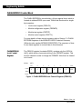
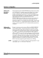
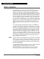
Order this document
by EB183/D
REV. 1.0
Motorola Semiconductor Engineering Bulletin
EB183
Erasing and Programming the FLASH EEPROM
on the MC68HC912B32
By Matt Ruff
M68HC11 and M68HC12 Applications
Austin, Texas
Introduction
This document outlines basic routines to program the FLASH EEPROM
through the background debug mode interface (BDM) using a Motorola
serial debug interface (SDIL) and the SDBUG12 (version 2.15) software
from P & E Microcomputer Systems, Inc.
One of the reasons the MC68HC912B32 device is so useful is that it
contains 32 Kbytes of embedded FLASH EEPROM. This module serves
as electrically programmable and erasable, non-volatile ROM emulation
memory, allowing for storage of program code which must be executed
frequently, must execute at high speeds, or which might need to be
upgraded in the field at a later time. Commonly used code segments,
such as standard subroutines or even operating systems, as well as
static data tables can be stored in the FLASH EEPROM.
© Motorola, Inc., 1998
EB183 — Rev. 1.0
Engineering Bulletin
FLASH EEPROM Control Block
The FLASH EEPROM is controlled by a 4-byte register block, which is
located at address $00F4 upon reset. Within this block are four singlebyte registers:
•
Lock control register (FEELCK)
•
Module configuration register (FEEMCR)
•
Module test register (FEETST)
•
Module control register (FEECTL)
For more detail on these control registers, refer to Section 7.4 FLASH
EEPROM Registers of the MC68HC912B32 Technical Summary
(Motorola order number MC68HC912B32TS/D). The sequence of how
to use these registers is covered later in this document.
FLASH EEPROM
Lock Control
Register
The FEELCK register (located at $00F4) contains only the LOCK bit
(bit 0), which allows or prevents writing to the FEEMCR register. This
must be cleared in order to change the FEEMCR. Note that it is cleared
out of reset.
Address:
$00F4
Bit 7
6
5
4
3
2
1
Bit 0
0
0
0
0
0
0
0
LOCK
0
0
0
0
0
0
0
0
Read:
Write:
Reset:
Figure 1. FLASH EEPROM Lock Control Register (FEELCK)
EB183 — Rev. 1.0
2
MOTOROLA
Engineering Bulletin
FLASH EEPROM Control Block
FLASH EEPROM
Module
Configuration
Register
The FEEMCR register (located at $00F5) contains only the BOOTP bit
(bit 0), which protects the 2-Kbyte boot block (1 Kbyte in early mask sets
G86W or G75R) located at $7800–$7FFF or $F800–$FFFF, depending
on the mapped location of the FLASH array at power-up. This bit must
be cleared, after the FEELCK (LOCK bit) is cleared, in order to write or
erase the boot block.
Address:
$00F5
Bit 7
6
5
4
3
2
1
Bit 0
0
0
0
0
0
0
0
BOOTP
0
0
0
0
0
0
0
1
Read:
Write:
Reset:
Figure 2. FLASH EEPROM Module Configuration Register (FEEMCR)
FLASH EEPROM
Module Test
Register
The FEETST register (located at $00F6) has no effect and always reads
0 in normal modes of operation.
Address:
$00F6
Bit 7
6
5
4
3
2
1
Bit 0
0
0
0
0
0
0
0
0
0
0
0
0
0
0
0
0
Read:
Write:
Reset:
Figure 3. FLASH EEPROM Module Test Register (FEETST)
EB183 — Rev. 1.0
MOTOROLA
3
Engineering Bulletin
FLASH EEPROM
Control Register
The FEECTL register (located at $00F7) controls the actual
programming and erasing of the FLASH EEPROM. In this register, five
bits are used to control the FLASH. All bits are 0 upon reset.
Address:
$00F7
Bit 7
6
5
4
3
2
1
Bit 0
0
0
0
FEESWAI
SVFP
ERAS
LAT
ENPE
0
0
0
0
0
0
0
0
Read:
Write:
Reset:
Figure 4. FLASH EEPROM Control Register (FEECTL)
FEESWAI
FEESWAI (bit 4) controls the behavior of the FLASH EEPROM clock
while in wait mode.
SVFP
SVFP (bit 3), the VFP status bit, is set when VFP is at or above normal
programming voltage levels; clear otherwise (read only)
ERAS
ERAS (bit 2), when set, configures the array for erasure.
LAT
LAT (bit 1), when set, enables the programming latches.
ENPE
ENPE (bit 0), when set, applies the programming/erase voltage to the
array.
EB183 — Rev. 1.0
4
MOTOROLA
Engineering Bulletin
Hardware Configuration
Hardware Configuration
Setting up the
Debugging
Hardware
Since programming the FLASH EEPROM takes a finite amount of time
and is dependent on a reliable programming voltage from an exterior
source, it is difficult to tell if the procedure worked immediately. To
simplify the debugging of the process, try using a few hardware tricks
that are listed in this bulletin. For debugging hardware, simply use an
light-emitting diode (LED) connected to a port pin on the
MC68HC912B32 device that blinks when an error is encountered, as
well as an LED attached to another port pin which lights when the
process is complete. For use with the code in this bulletin, connect a red
LED to PA0, with a 1-KΩ current limiting resistor to indicate errors. In like
manner, connect a green LED to PA1 to indicate that the process has
completed.
Setting up the
M68HC12B32EVB
Be sure to connect your VFP source to W8 on the M68HC12B32EVB
with the proper polarity. The ground should be connected to the pin
closest to the edge of the board and farthest from the microcontroller.
This applies VFP to the board, but the jumper on W7 actually transfers
VFP to the VFP pin (pin 69) on the microcontroller. When a jumper is
placed on the left two pins of W7 (with board facing so that silk screening
can be read), VFP is connected to the chip. When the jumper is moved
to the right, so that the center pin and right pin are shorted, then VDD is
applied to the chip. This is the default location, and a jumper should
always be located here to maintain the voltage on the VFP pin on the
MCU at VDD when programming and erasing are not occurring.
NOTE:
VFP should be 11.4–11.8 volts for mask sets 1H91F and 3H91F. For all
other masks, use 11.4–12.6 volts (12 volts ±5%).
EB183 — Rev. 1.0
MOTOROLA
5
Engineering Bulletin
Software Considerations
Using SDBUG12 to manipulate the FLASH EEPROM requires some
special considerations. First, a few bugs in some versions of the
software can cause some confusion when manipulating the FLASH
memory array. The memory display windows sometimes do not refresh
properly, especially when manually erasing the array by manipulating
the control registers using the mm command. Once the erase voltage
has been applied by modifying the FEECTL register, the display often
shows all of the odd addresses as one value and all the even addresses
as another value. To fix this problem, issue a reset command from the
SDBUG12 command prompt to force SDBUG12 to refresh all of its
display windows from the microcontroller once the part comes out of
reset.
The routines that follow were tested with version 2.15 of SDBUG12
running on a Windows NT workstation in a DOS window. The problem
described in the preceding paragraph did not appear when executing
these routines. SDBUG12 displayed the proper values for the FLASH
array when the routines were allowed to run to completion. The code
segments included here can both be loaded into the RAM of the part,
using the load command in SDBUG12. Notice that the entry point of the
program routine is $80A and the entry point of the erase routine is $90A.
Once loaded into RAM, g 80A will begin the programming process or
g 90A will begin the erase process.
NOTE:
Once the FLASH array has been erased or programmed, reloading the
DBUG12 monitor into the FLASH array is necessary if you wish to use
it, as manipulation of the array will destroy the monitor program code.
This can be accomplished with the bootloader in the boot block of the
part or by using Prog12s.
If using the M68EVB912B32 evaluation board, refer to Appendix E of the
Evaluation Board User’s Manual (Motorola order number
68EVB912B32UM/D), for further information on how to reload the
monitor program into the device using the on-board bootloader.
EB183 — Rev. 1.0
6
MOTOROLA
Engineering Bulletin
Erasing the FLASH Array
Erasing the FLASH Array
This code segment follows the recommended procedure for erasing the
FLASH array. Following the code is a flowchart which outlines this same
procedure. The general idea is to apply the erase voltage to the FLASH
module within the chip (by setting the ENPE bit), set the erase flag, write
to any location in the array, then check to make sure the entire array is
erased. If the whole array is erased, then the number of times the erase
voltage was applied to get this erasure will have been preserved in the
Nep variable. The erase voltage is then pulsed that many times again to
ensure that the array remains erased. This is 100% erase margin.
NOTE:
In the following code, the STEP labels refer to Section 7.7 of the
MC68HC912B32 Technical Summary (Motorola order number
MC68HC912B32TS/D).
;-------------------------------------------------------;--- FLASH EEPROM erase routine
--;----;--- Rev. 1.0 April 16,1998
--;--Changed to 100ms delay for tepulse
--;--- Written November 6, 1997
--;----;-------------------------------------------------------;---- Equates
FEELCK EQU
FEEMCR EQU
FEECTL EQU
FEESTART EQU
FEEEND EQU
MAXNep EQU
;---- Equates
----------------------$F4
$F5
$F7
$8000
;FLASH Start address
$FFFF
;FLASH End address
!5
;5 pulses maximum
-----------------------
ORG
Nep
DS
MARGINF DS
ERASED DS
$0900
1
1
1
START
ORG
LDS
LDX
CLR
CLR
CLR
$90A
#$B00
#$0000
Nep
MARGINF
ERASED
;Number of programming pulses applied
;Programming margin flag
;Array Erased Flag
;(Turn on Vfp supply to board here)
;Clear number of pulses
;Clear margin flag
;Clear erased flag
EB183 — Rev. 1.0
MOTOROLA
7
Engineering Bulletin
STEP2
STEP3
STEP4
STEP5
STEP6
STEP7
MOVB
BRCLR
LDAB
STAB
BSET
JSR
BCLR
JSR
LDAA
CMPA
BNE
#$06,FEECTL
;Set ERAS and set LAT in FEECTL
FEECTL,$08,ERROR ;If Vfp not present, output an error
#$FF
FEESTART,X
;Write data to a valid Flash address
FEECTL,$01
;Apply erase voltage (Set ENPE)
dly_100ms
;Delay time for erase pulse (Tepulse)
FEECTL,$01
;Remove erase voltage (Clear ENPE)
dly_10ms
;Delay for high voltage turn off (Tverase)
#$01
MARGINF
;Is margin flag set??
NOFLAG
;If not, go bump counter and check data
YESFLAG DEC
LDAA
CMPA
BNE
JSR
LDAA
CMPA
BEQ
STEP10 BCLR
BRA
Nep
#$00
Nep
STEP4
READARRY
#$01
ERASED
ERROR
FEECTL,$02
DONE
;Decrement Nep
NOFLAG
Nep
READARRY
#$00
ERASED
SETMARF
Nep
#MAXNep
STEP4
ERROR
;Increment number of erase pulses applied
;Verify entire array is erased
SETMARF INC
BRA
MARGINF
STEP4
;Set Margin Flag
DONE
#$00,$0000
#$FF,$0002
#$02,$0000
DONE
;Clear Port A
;Set DDRA to outputs
;Turn on PA1 to indicate complete
;(Turn off Vfp)
INC
BSR
LDAA
CMPA
BEQ
LDAB
CMPB
BLS
BSR
MOVB
MOVB
MOVB
BRA
;Is Nep=0?
;If not, go to Step 4
;Verify entire array is erased
;Is the array erased?
;Erase failed, output an error
;Clear LAT in FEECTL
;If so, quit.
;Is it erased?
;If so, set margin flag
;Have we applied max number of pulses?
;If not, continue erasing
;If so, we have a problem
EB183 — Rev. 1.0
8
MOTOROLA
Engineering Bulletin
Erasing the FLASH Array
;-----------------------------------------------;---Read and Verify Erase subroutine
---;-----------------------------------------------READARRY LDY
#$FFFF
LDX
#FEESTART
LOOP
CPY
0,X
;Is this word erased?
BNE
EXITverf
;If not, leave without setting flag
CPX
#FEEEND
;Are we at the end of the array?
BEQ
EXITverf
INX
;Go to the next address
INX
BRA
LOOP
INC
ERASED
;Set erased flag
EXITverf RTS
;-----------------------------------------------;--------Error Subroutine
------------;-----------------------------------------------ERROR: MOVB
#$00,$0000
;Clear Port A
MOVB
#$FF,$0002
;Set DDRA to outputs
BLINK
MOVB
#$01,$0000
;Turn PA0 on for error output
BSR
dly_100ms
BSR
dly_100ms
BSR
dly_100ms
MOVB
#$00,$0000
;Turn PA0 off
BSR
dly_100ms
BSR
dly_100ms
BSR
dly_100ms
BRA
BLINK
; Repeat ad nauseum....
;------------------------------------------------------------;--------Delay Subroutines (8MHz e clock) ------------;------------------------------------------------------------dly_100ms: LDY
#$000A
; Delay for 100ms (8MHz E clock)
DLOOP10: DEY
BSR
dly_10ms
BNE
DLOOP10
RTS
dly_10ms: LDD
DLOOP: SUBD
BNE
RTS
#$3E7E
#1
DLOOP
; Delay for 10ms (8MHz E clock)
END
EB183 — Rev. 1.0
MOTOROLA
9
Engineering Bulletin
START ERASE
TURN ON VFP
CLEAR MARGIN FLAG
CLEAR ERASE PULSE COUNTER (nEP)
SET ERAS
SET LAT
WRITE TO ARRAY
SET ENPE
DELAY FOR DURATION
OF ERASE PULSE
(tEPULSE)
CLEAR ENPE
SET
MARGIN FLAG
DELAY BEFORE VERIFY
(tVERASE)
IS
MARGIN FLAG
SET?
NO
INCREMENT
nEP COUNTER
READ
ARRAY
YES
DECREMENT
nEP COUNTER
ARRAY
ERASED?
YES
NO
NO
nEP = 0?
nEP = 5?
YES
ARRAY
ERASED?
NO
YES
NO
YES
CLEAR LAT
TURN OFF VFP
ARRAY ERASED
ARRAY FAILED TO ERASE
Figure 5. Erase Sequence Flow
EB183 — Rev. 1.0
10
MOTOROLA
Engineering Bulletin
Programming the FLASH Array
Programming the FLASH Array
The following code segment follows the recommended procedure for
programming the FLASH array. Following the code is a flowchart which
outlines this same procedure. The general idea is to apply the
programming voltage to the FLASH module within the chip (by setting
the ENPE bit), set the programming latches, write the desired byte/word
to the location in the array, then check to make sure the location is
programmed properly. If the data is correct, then the number of times the
programming voltage was applied to get this byte programmed will have
been preserved in the NPP variable. The programming voltage is then
pulsed that many times again to ensure that the byte/word remains
programmed. This is 100% programming margin. This whole process is
repeated for each byte/word to be programmed. The code segment
below simply copies a string of characters from RAM and stores it at the
beginning of the FLASH array.
NOTE:
In the following code, the STEP labels refer to Section 7.6 of the
MC68HC912B32 Technical Summary (Motorola order number
MC68HC912B32TS/D).
;-------------------------------------------------------;--- FLASH EEPROM program routine
--;----;--- Rev. 1.0 - April 23,1998
--;--Fixed Tppulse = 25µs and Tvprog = 10µs
--;--- Written November 6, 1997
--;----;--------------------------------------------------------
;-------------FEELCK EQU
FEEMCR EQU
FEECTL EQU
FEESTART EQU
FEEEND EQU
MAXNpp EQU
Equates ----------------$F4
$F5
$F7
$8000
;FLASH Start address
$FFFF
;FLASH End address
!50
;50 pulses maximum
ORG
Npp
DS
MARGINF DS
$0800
1
1
ORG
;Number of programming pulses applied
;Programming margin flag
$80A
EB183 — Rev. 1.0
MOTOROLA
11
Engineering Bulletin
START
LDS
BRCLR
LDX
#$B00
;(Turn on your Vfp power supply to board)
FEECTL,$08,ERROR ;If Vfp not present, output an error
#$0000
LOOP
CLR
CLR
MOVB
LDAB
STAB
BSET
JSR
BCLR
JSR
LDAA
CMPA
BNE
Npp
MARGINF
#$02,FEECTL
DATA,X
FEESTART,X
FEECTL,$01
dly_22us
FEECTL,$01
dly_10us
#$01
MARGINF
NOFLAG
;Clear number of pulses
;Clear margin flag
;Clear ERAS and set LAT in FEECTL
YESFLAG DEC
LDAA
CMPA
BNE
STEP9
LDAA
CMPA
BNE
STEP10 BCLR
INX
CMPA
BNE
BRA
Npp
#$00
Npp
STEP4
FEESTART,X
DATA,X
ERROR
FEECTL,$02
;Decrement Npp
#$00
LOOP
DONE
;Check to see if we're done
;If not, go back to start!
;If so, quit.
NOFLAG
Npp
FEESTART,X
DATA,X
SETMARF
Npp
#MAXNpp
STEP4
ERROR
;Increment number of prog pulses applied
;Read FEEPROM location to verify programming
;Is it the same as the byte to be programmed?
;If so, set the margin flag
SETMARF INC
BRA
MARGINF
STEP4
;Set Margin Flag
DONE
#$00,$0000
#$FF,$0002
#$02,$0000
*
;Clear Port A
;Set DDRA to outputs
;Turn on PA1 to indicate complete
;(Turn off Vfp supply - programming complete)
STEP2
STEP3
STEP4
STEP5
STEP6
STEP7
INC
LDAA
CMPA
BEQ
LDAB
CMPB
BLS
BSR
MOVB
MOVB
MOVB
BRA
;Write data to address
;Apply programming voltage (Set ENPE)
;Delay time for prog pulse (Tppulse)
;Remove programming voltage (Clear ENPE)
;Delay for high voltage turn off (Tvprog)
;Is margin flag set??
;If not, go bump counter and check data
;Is Npp=0?
;If not, go to Step 4
;Read FEEPROM location to verify programming
;Is it the same as the byte to be programmed?
;Programming failed, output an error
;Clear LAT in FEECTL
;Have we applied max number of pulses?
;If not, continue programming
;If so, we have a problem
EB183 — Rev. 1.0
12
MOTOROLA
Engineering Bulletin
Programming the FLASH Array
;-----------------------------------------------;--------Error Subroutine
------------;-----------------------------------------------ERROR: MOVB
#$00,$0000
;Clear Port A
MOVB
#$FF,$0002
;Set DDRA to outputs
BLINK
MOVB
#$01,$0000
;Turn PA0 on for error output
BSR
dly_100ms
BSR
dly_100ms
BSR
dly_100ms
MOVB
#$00,$0000
;Turn PA0 off
BSR
dly_100ms
BSR
dly_100ms
BSR
dly_100ms
BRA
BLINK
; Repeat ad nauseum....
;------------------------------------------------------------;--------Delay Subroutines (8MHz e clock) ------------;------------------------------------------------------------dly_100ms: LDY
#$000A
; Delay for 100ms
DLOOP10: DEY
BSR
dly_10ms
BNE
DLOOP10
RTS
dly_10ms: LDD
DLOOP: SUBD
BNE
RTS
#$3E7E
#1
DLOOP
; Delay for 10ms
dly_22us: LDD
d_22u
SUBD
BNE
RTS
#$0023
#1
d_22u
; Delay for almost 22µs
dly_10us: LDD
d_10u
SUBD
BNE
RTS
#$0010
#1
d_10u
; Delay for 10µs
DATA
"Motorola Microcontrollers"
$00
FCB
FCB
END
EB183 — Rev. 1.0
MOTOROLA
13
Engineering Bulletin
START PROG
TURN ON VFP
CLEAR MARGIN FLAG
CLEAR PROGRAM PULSE COUNTER (nPP)
CLEAR ERAS
SET LAT
WRITE DATA
TO ADDRESS
SET ENPE
DELAY FOR DURATION
OF PROGRAM PULSE
(tPPULSE)
CLEAR ENPE
SET
MARGIN FLAG
DELAY BEFORE VERIFY
(tVPROG)
IS
MARGIN FLAG
SET?
NO
INCREMENT
nPP COUNTER
READ
LOCATION
YES
DECREMENT
nPP COUNTER
DATA
CORRECT?
YES
NO
NO
nPP = 0?
nPP = 50?
YES
DATA
CORRECT?
NO
YES
NO
YES
CLEAR LAT
GET NEXT
ADDRESS/DATA
NO
LOCATION FAILED
TO PROGRAM
DONE?
YES
TURN OFF VFP
DONE PROG
Figure 6. Program Sequence Flow
EB183 — Rev. 1.0
14
MOTOROLA
Engineering Bulletin
Conclusion
Conclusion
This bulletin gives an overview of the basics of erasing and programming
the FLASH array on the MC68HC912B32 microcontroller. Knowing
these basics, it is easy to progress to writing a bootloader, designing a
field programming unit, or anything else needed to manipulate the
FLASH memory.
For an example of a serial bootloader for this microcontroller, refer to
Serial Bootloader for Reprogramming the MC68HC912B32 FLASH
EEPROM (Motorola order number AN1718/D).
EB183 — Rev. 1.0
MOTOROLA
15
N O N - D I S C L O S U R E
A G R E E M E N T
R E Q U I R E D
Engineering Bulletin
Motorola reserves the right to make changes without further notice to any products herein. Motorola makes no warranty, representation or guarantee regarding the suitability of its
products for any particular purpose, nor does Motorola assume any liability arising out of the application or use of any product or circuit, and specifically disclaims any and all liability,
including without limitation consequential or incidental damages. "Typical" parameters which may be provided in Motorola data sheets and/or specifications can and do vary in different
applications and actual performance may vary over time. All operating parameters, including "Typicals" must be validated for each customer application by customer's technical experts.
Motorola does not convey any license under its patent rights nor the rights of others. Motorola products are not designed, intended, or authorized for use as components in systems
intended for surgical implant into the body, or other applications intended to support or sustain life, or for any other application in which the failure of the Motorola product could create a
situation where personal injury or death may occur. Should Buyer purchase or use Motorola products for any such unintended or unauthorized application, Buyer shall indemnify and hold
Motorola and its officers, employees, subsidiaries, affiliates, and distributors harmless against all claims, costs, damages, and expenses, and reasonable attorney fees arising out of,
directly or indirectly, any claim of personal injury or death associated with such unintended or unauthorized use, even if such claim alleges that Motorola was negligent regarding the
design or manufacture of the part. Motorola and
are registered trademarks of Motorola, Inc. Motorola, Inc. is an Equal Opportunity/Affirmative Action Employer.
How to reach us:
USA/EUROPE/Locations Not Listed: Motorola Literature Distribution, P.O. Box 5405, Denver, Colorado 80217, 1-800-441-2447 or
1-303-675-2140. Customer Focus Center, 1-800-521-6274
JAPAN: Nippon Motorola Ltd.: SPD, Strategic Planning Office, 141, 4-32-1 Nishi-Gotanda, Shinigawa-Ku, Tokyo, Japan. 03-5487-8488
ASIA/PACIFIC: Motorola Semiconductors H.K. Ltd., 8B Tai Ping Industrial Park, 51 Ting Kok Road, Tai Po, N.T., Hong Kong. 852-26629298
Mfax™, Motorola Fax Back System: [email protected]; http://sps.motorola.com/mfax/;
TOUCHTONE, 1-602-244-6609; US and Canada ONLY, 1-800-774-1848
HOME PAGE: http://motorola.com/sps/
Mfax is a trademark of Motorola, Inc.
© Motorola, Inc., 1998
EB183/D