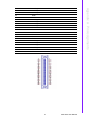
1
User Manual MIO-5270 Copyright The documentation and the software included with this product are copyrighted 2011 by Advantech Co., Ltd. All rights are reserved. Advantech Co., Ltd. reserves the right to make improvements in the products described in this manual at any time without notice. No part of this manual may be reproduced, copied, translated or transmitted in any form or by any means without the prior written permission of Advantech Co., Ltd. Information provided in this manual is intended to be accurate and reliable. However, Advantech Co., Ltd. assumes no responsibility for its use, nor for any infringements of the rights of third parties, which may result from its use. Acknowledgements AMD is a trademark of Advanced Micro Devices. Award is a trademark of Award Software International, Inc. VIA is a trademark of VIA Technologies, Inc. IBM, PC/AT, PS/2 and VGA are trademarks of International Business Machines Corporation. Microsoft Windows is a registered trademark of Microsoft Corp. RTL is a trademark of Realtek Semi-Conductor Co., Ltd. ESS is a trademark of ESS Technology, Inc. UMC is a trademark of United Microelectronics Corporation. SMI is a trademark of Silicon Motion, Inc. Creative is a trademark of Creative Technology LTD. CHRONTEL is a trademark of Chrontel Inc. All other product names or trademarks are properties of their respective owners. MIO-5270 User Manual Part No. 2006527010 Edition 1 Printed in China October 2011 ii Product Warranty (2 years) Advantech warrants to you, the original purchaser, that each of its products will be free from defects in materials and workmanship for two years from the date of purchase. This warranty does not apply to any products which have been repaired or altered by persons other than repair personnel authorized by Advantech, or which have been subject to misuse, abuse, accident or improper installation. Advantech assumes no liability under the terms of this warranty as a consequence of such events. Because of Advantech’s high quality-control standards and rigorous testing, most of our customers never need to use our repair service. If an Advantech product is defective, it will be repaired or replaced at no charge during the warranty period. For outof-warranty repairs, you will be billed according to the cost of replacement materials, service time and freight. Please consult your dealer for more details. If you think you have a defective product, follow these steps: 1. Collect all the information about the problem encountered. (For example, CPU speed, Advantech products used, other hardware and software used, etc.) Note anything abnormal and list any onscreen messages you get when the problem occurs. 2. Call your dealer and describe the problem. Please have your manual, product, and any helpful information readily available. 3. If your product is diagnosed as defective, obtain an RMA (return merchandise authorization) number from your dealer. This allows us to process your return more quickly. 4. Carefully pack the defective product, a fully-completed Repair and Replacement Order Card and a photocopy proof of purchase date (such as your sales receipt) in a shippable container. A product returned without proof of the purchase date is not eligible for warranty service. 5. Write the RMA number visibly on the outside of the package and ship it prepaid to your dealer. Declaration of Conformity FCC Class A Note: This equipment has been tested and found to comply with the limits for a Class A digital device, pursuant to part 15 of the FCC Rules. These limits are designed to provide reasonable protection against harmful interference when the equipment is operated in a commercial environment. This equipment generates, uses, and can radiate radio frequency energy and, if not installed and used in accordance with the instruction manual, may cause harmful interference to radio communications. Operation of this equipment in a residential area is likely to cause harmful interference in which case the user will be required to correct the interference at his own expense. iii MIO-5270 User Manual Technical Support and Assistance 1. 2. Visit the Advantech web site at www.advantech.com where you can find the latest information about the product. Contact your distributor, sales representative, or Advantech's customer service center for technical support if you need additional assistance. Please have the following information ready before you call: – Product name and serial number – Description of your peripheral attachments – Description of your software (operating system, version, application software, etc.) – A complete description of the problem – The exact wording of any error messages Warnings, Cautions and Notes Warning! Warnings indicate conditions, which if not observed, can cause personal injury! Caution! Cautions are included to help you avoid damaging hardware or losing data. e.g. There is a danger of a new battery exploding if it is incorrectly installed. Do not attempt to recharge, force open, or heat the battery. Replace the battery only with the same or equivalent type recommended by the manufacturer. Discard used batteries according to the manufacturer's instructions. Note! Notes provide optional additional information. Document Feedback To assist us in making improvements to this manual, we would welcome comments and constructive criticism. Please send all such - in writing to: [email protected] MIO-5270 User Manual iv Packing List Before setting up the system, check that the items listed below are included and in good condition. If any item does not accord with the table, please contact your dealer immediately. 1 x MIO-5270 SBC 1 x SATA Cable 30cm (P/N 1700006291) 1 x SATA Power Cable 35cm (P/N 1700018785) 1 x Audio Cable 20cm (P/N 1700019584) 2 x COM Cable 22cm (P/N 1701200220) 1 x COM RS-422/485 Cable 25cm (P/N 1700019435) 1 x Heatsink (25mm) for T40E/T40R (P/N 1960053507N001) 1 x Cooler (25mm) for T56N (P/N 1960053508N001) Startup Manual CD-ROM (Manual, Driver, Utility) 1 x Mini Jumper(10pcs package) (P/N 9689000002) Ordering Information Model Number Description MIO-5270D-S6A1E AMD T56N 1.65G Dual Core + HudsonM1 MIO-5270D-S0A1E AMD T40E 1.0G Dual Core + HudsonM1 MIO-5270S-S0A1E AMD T40R 1.0G Single Core + HudsonM1 MIO-5270S-S0A1E MIO-5270D-S0A1E MIO-5270D-S6A1E CPU AMD T40R 1.0G SC AMD T40E 1.0G DC AMD T56N 1.65G DC L2 Cache 512 KB L2 512 KB L2 1 MB L2 LVDS 48-bit 48-bit 48-bit VGA Yes Yes Yes HDMI Yes Yes Yes GbE 2 2 2 Audio Yes Yes Yes RS-232/422/485 1 1 1 RS-232 3 3 3 USB 2.0 6 6 6 GPIO 8-bit 8-bit 8-bit SATAII 2 2 2 Cfast 1 1 1 PCIe Mini Card* 1 1 1 MIOe Yes Yes Yes Thermal Solution Passive Passive Active Operational Temp. 0 ~ 60° C 0 ~ 60° C 0 ~ 60° C * mSATA is optional alternative by request v MIO-5270 User Manual Optional MIOe Module Part Number Description MIOe-210-D6A1E 4x RS232/422/485 2x RS422/485 with DSUB connector, 8-bit GPIO MIOe-210-W6A1E 4x RS232/422/485 2x RS422/485 with Wafer connector, 8-bit GPIO MIOe-220-L3A1E 3 x GbE with RJ45 connector MIOe-220-B3A1E 3 x GbE with RJ45 connector through PCIE switch MIOe-230-L0A1E* Displayport to 48-bit LVDS MIOe-230-D0A1E* Displayport to Ext. Displayport *MIOe-230 compatibility is optional by request. Optional Accessories Part number Description 1960054266T001 Heat spreader AMD-Ontario 137x84.2x16.7-SC MIO-5270 1703100260 Internal USB 5/6 cable 1935032000 Screw of Heatsink / Cooler R/S 5.5 2.0 +M M3*20L ST Ni 1910002088 The POST Stand off, F=M3*6L M=M3*5L B=5 H=16 Ni 1757003082 Adapter 100-240V 60W 12V 5A W/O PFC Safety Instructions 1. 2. 3. 4. 5. 6. 7. 8. 9. 10. 11. 12. 13. Read these safety instructions carefully. Keep this User Manual for later reference. Disconnect this equipment from any AC outlet before cleaning. Use a damp cloth. Do not use liquid or spray detergents for cleaning. For plug-in equipment, the power outlet socket must be located near the equipment and must be easily accessible. Keep this equipment away from humidity. Put this equipment on a reliable surface during installation. Dropping it or letting it fall may cause damage. The openings on the enclosure are for air convection. Protect the equipment from overheating. DO NOT COVER THE OPENINGS. Make sure the voltage of the power source is correct before connecting the equipment to the power outlet. Position the power cord so that people cannot step on it. Do not place anything over the power cord. All cautions and warnings on the equipment should be noted. If the equipment is not used for a long time, disconnect it from the power source to avoid damage by transient overvoltage. Never pour any liquid into an opening. This may cause fire or electrical shock. Never open the equipment. For safety reasons, the equipment should be opened only by qualified service personnel. MIO-5270 User Manual vi 14. If one of the following situations arises, get the equipment checked by service personnel: The power cord or plug is damaged. Liquid has penetrated into the equipment. The equipment has been exposed to moisture. The equipment does not work well, or you cannot get it to work according to the user's manual. The equipment has been dropped and damaged. The equipment has obvious signs of breakage. 15. DO NOT LEAVE THIS EQUIPMENT IN AN ENVIRONMENT WHERE THE STORAGE TEMPERATURE MAY GO BELOW -20° C (-4° F) OR ABOVE 60° C (140° F). THIS COULD DAMAGE THE EQUIPMENT. THE EQUIPMENT SHOULD BE IN A CONTROLLED ENVIRONMENT. 16. CAUTION: DANGER OF EXPLOSION IF BATTERY IS INCORRECTLY REPLACED. REPLACE ONLY WITH THE SAME OR EQUIVALENT TYPE RECOMMENDED BY THE MANUFACTURER, DISCARD USED BATTERIES ACCORDING TO THE MANUFACTURER'S INSTRUCTIONS. The sound pressure level at the operator's position according to IEC 704-1:1982 is no more than 70 dB (A). DISCLAIMER: This set of instructions is given according to IEC 704-1. Advantech disclaims all responsibility for the accuracy of any statements contained herein. Safety Precaution - Static Electricity Follow these simple precautions to protect yourself from harm and the products from damage. To avoid electrical shock, always disconnect the power from your PC chassis before you work on it. Don't touch any components on the CPU card or other cards while the PC is on. Disconnect power before making any configuration changes. The sudden rush of power as you connect a jumper or install a card may damage sensitive electronic components. vii MIO-5270 User Manual MIO-5270 User Manual viii Contents Chapter Chapter 1 General Information ............................1 1.1 1.2 1.3 Introduction ............................................................................................... 2 Product Specifications............................................................................... 2 Chipset ...................................................................................................... 3 1.3.1 Functional Specifications .............................................................. 3 1.3.2 Mechanical Specifications............................................................. 5 1.3.3 Electrical Specifications ................................................................ 6 1.3.4 Environmental Specifications........................................................ 6 2 Hardware Installation ..........................7 2.1 Jumpers .................................................................................................... 8 2.1.1 Jumper List ................................................................................... 8 2.1.2 Jumper Settings ............................................................................ 8 2.1.3 Jumper Description ....................................................................... 9 Connectors.............................................................................................. 10 2.2.1 Connector List............................................................................. 10 Mechanical .............................................................................................. 11 2.3.1 Jumper and Connector Location................................................. 11 Figure 2.1 Jumper and Connector Layout (Component Side) ... 11 Figure 2.2 Jumper and Connector Layout (Solder Side) ........... 12 2.3.2 Board Dimensions....................................................................... 13 Figure 2.3 Board Dimension Layout (Component Side) ............ 13 Figure 2.4 Board Dimension Layout (Solder Side) .................... 13 Figure 2.5 I/O Connectors Mechanical Drawing ........................ 14 2.2 2.3 Chapter 3 BIOS Settings.....................................15 3.1 3.2 3.5 3.6 3.7 Entering Setup ........................................................................................ 16 Main Setup .............................................................................................. 17 3.2.1 System date / System time ......................................................... 17 Advanced BIOS Features Setup ............................................................. 18 3.3.1 PCI Subsystem Settings Configuration....................................... 19 3.3.2 ACPI Settings Configuration ....................................................... 20 3.3.3 CPU Configuration ...................................................................... 21 3.3.4 IDE Configuration........................................................................ 22 3.3.5 USB Configuration ...................................................................... 22 3.3.6 Embedded Controller Configuration............................................ 23 3.3.7 Super I/O Configuration .............................................................. 24 Chipset Configuration.............................................................................. 25 3.4.1 North Bridge Configuration ......................................................... 26 3.4.2 Display Configuration Select....................................................... 27 3.4.3 South Bridge ............................................................................... 28 Boot Configuration .................................................................................. 29 Security Configuration............................................................................. 30 Save & Exit.............................................................................................. 31 4 MIOe Installation ................................33 Appendix A Pin Assignments ...............................35 3.3 3.4 Chapter ix MIO-5270 User Manual Appendix B System Assignment.......................... 57 B.1 System I/O Ports..................................................................................... 58 Table B.1: System I/O Ports ...................................................... 58 1st MB memory map............................................................................... 58 Table B.2: 1st MB memory map ................................................ 58 Interrupt assignments ............................................................................. 59 Table B.3: Interrupt assignments............................................... 59 B.2 B.3 Appendix C Watchdog Timer Sample Code ........ 61 C.1 EC Watchdog Timer sample code .......................................................... 62 Appendix D AMD G-Series .................................... 63 MIO-5270 User Manual x Chapter 1 1 General Information 1.1 Introduction CPU: AMD G-series eOntario – T56N (Dual Core 1.65GHz) on MIO-5270D-S6A1E – T40E (Dual Core 1.0GHz) on MIO-5270D-S0A1E – T40R (Single Core 1.0GHz) on MIO-5270S-S0A1E MIO Compact SBC form factor standard One 204-pin SODIMM DDR3 up to 4G – T56N: DDR3 1333 MHz – T40E/T40R: DDR3 1066 MHz Dual Independent Display: VGA+LVDS, VGA+HDMI, HDMI+LVDS 6 x USB 2.0 ports 2 x SATAII (Max data transfer rate 300 MB/s) 4 x COM (3 x RS-232, 1 x RS-232/422/485) Multi level Watchdog timer (set by Advantech iManager) 2 x GbE MIOe 2.0 connector Wake-on-LAN, Wake-on-Modem 1.2 Product Specifications General CPU AMD G-Series: T56N (Dual Core 1.65GHz) on MIO-5270D-S6A1E T40E (Dual Core 1.0GHz) on MIO-5270D-S0A1E T40R (Single Core 1.0GHz) on MIO-5270S-S0A1E L2 Cache T56N: 1MB T40E/T40R: 512KB System Chipset AMD G-series + A50M FCH BIOS AMI EFI 32-Mbit System Memory 1 x 204-pin SODIMM socket DDR3 up to 4GB: T56N up to DDR3 1333 MHz T40E/T40R up to DDR3 1066 MHz Power Management APM1.2, ACPI support SSD mSATA*, CFast Watchdog Timer 255 levels timer interval, programmable by software. Multi level WDT (set by iManager) Expansion Interface PCIe Mini Card, CFast, MIOe Battery Lithium 3 V / 210 mAH *mSATA is optional alternative by request. I/O Internal I/O Interface 2 x SATAII, 3 x RS-232, 1 x RS232/422/485, 2 x USB 2.0, GPIO, SMBus Rear I/O 4 x USB 2.0, HDMI, VGA, 2 x RJ45 Ethernet, DC Power-in Power Connector T56N: 2 x 2 pin power connector T40E/T40R: DC Jack SMBus Supported GPIO 8-bit general purpose input/output MIO-5270 User Manual 2 Speed GbE 10/100/1000 Mbps Chipset Realtek RTL8111E- VB-GR (GbE1, GbE2) Ethernet Interface Fully compliant with IEEE 802.3, IEEE 802.3u, IEEE 802.3ab Connector: RJ45 x2 Chapter 1 Ethernet Display AMD G-series T56N/T40E/T40R VGA: Resolution Dual Independent Display – T56N: 2560 x 1600 – T40E/T40R: 1920 x 1200 LVDS: – LVDS supports single channel 24-bit/dual channels 48bit – T56N: 2560 x 1600 @ 60 Hz – T40E/T40R: 1920 x 1200 @ 60 Hz – (Pixel clock rate 80MHz) HDMI: – Supports 1920 x 1080p @ 60 Hz, 36bpp – Supports HDMI 1.3, using TMDS data encoding VGA+LVDS, VGA+HDMI, HDMI+LVDS 1.3 Chipset 1.3.1 Functional Specifications 1.3.1.1 Processor: AMD G-series T56N/T40E/T40R CPU Process 40nm – T56N: DDR3 1333 MHz – T40E/T40R: DDR3 1066 MHz FSB Memory SODIMM DDR3 up to 4G – T56N: DDR3 1333 MHz – T40E/T40R: DDR3 1066 MHz VGA Memory Up to 512MB of dynamic video memory allocation Internal Graphics Features DirectX® 11 graphics with UVD 3.0 Up to 2 Display Port/TMDS Integrated VGA DAC Displayport 1.1a Integrated Graphics Engine clock speed: 500 MHz or 280 MHz, dependent on OPN Dedicated graphics memory controller" 3 MIO-5270 User Manual General Information Controller Video Accelerator Display Dual independent display 2D Acceleration 3D Acceleration – Fully DirectX® 11 compliant, including full speed 32-bit floating point per component operations – Support for OpenCL™ 1.0 – Support for OpenGL® 3.2 and 2.1 Motion Video Acceleration – Supports DVD, Blu-ray*, and SDTV/HDTV content playback with the lowest CPU usage – H.264 implementation based on the ISO/IEC 14496-10 specification – VC-1 implementation based on the SMPTE 421M specification – MPEG2 implementation based on the IOS 138112 specification" VGA: T56N: 2560 x 1600 T40E/T40R: 1920 x 1200 LVDS: LVDS supports single channel 24-bit/dual channels 48-bit T56N: 2560 x 1600 @ 60Hz T40E/T40R: 1920 x 1200 @ 60Hz (Pixel clock rate 80MHz) HDMI: Supports 1920 x 1080p @ 60Hz, 36bpp Supports HDMI 1.3, using TMDS data encoding VGA+LVDS, VGA+HDMI, HDMI+LVDS 1.3.1.2 Chipset (Hudson M1) South Bridge Control Hub Hudson M1 RS-232 3 RS-232/422/485 1 K/B 1 Mouse 1 USB 6 x USB 2.0 Audio HD Audio, ALC892 Codec, Line-in, Line-out, Mic-in, speaker out (R/L) (Supports 8Ω 1W or 4Ω 2 W Speaker for Speaker-out) Other Features * 6 x USB 2.0 ports, 480MB/s (all internal connectors) Default: 500mA @ one port (Up to 1A @ 2 ports) * 2 x SATAII (Max. Data transfer Rate 300MB/s) * HD Audio CODEC (ALC892) * Power Management (S0, S3,S4, S5) BIOS 32-Mb Flash BIOS via SPI MIO-5270 User Manual 4 Chapter 1 1.3.1.3 iManager iManager Supported SMBus Supported GPIO 8-bit GPIO Watchdog timer Multi Level WDT (set by Advantech iManager) Programmable 1-255 sec / min Hardware monitor CPU Temperature / input Current / input Voltage Power saving Deep sleep S5 mode / Smart Fan / Back light control FAN 1. Smart FAN Support. 2. Programmable automatic fan monitor based on temperature. 3. Reserve CPU FAN Power Connector x 1 Pin2: +12 V Pin3: Fan speed signal input Board information Running HR / Boot record 1.3.1.4 Others Ethernet Chipset GbE1: Realtek 8111E-VB-GR 10/100/1000 Mbps GbE2: Realtek 8111E-VB-GR 10/100/1000 Mbps IEEE Compliant Fully compliant with IEEE 802.3, IEEE 802.3u, IEEE 802.3ab Disable LAN through BIOS Yes Driver Support WES7/Windows XP/XP Embed/CE, Linux, QNX Audio Codec HD Audio, Realtek ALC892 Connector Line in, Line out, Mic in, Speak out (R/L, 8 Ohm 1W/ 4Ohm 2W) Voltage 3.3V, +5V, +12V, Vcore 1.3.2 Mechanical Specifications 1.3.2.1 Dimensions (mm) 146 x 102 mm (5.7 x 4 inches) 1.3.2.2 Board height on Top side (mm) 16,4mm (Rear I/O USB) 1.3.2.3 Board height on bottom side (mm) 8.5mm (CF socket) 1.3.2.4 Heatsink/Cooler Dimensions (mm) 137mm (L) x 87.2mm (W) x 25mm (H) 1.3.2.5 Board net weight without heatsink (g) 140 g 5 MIO-5270 User Manual General Information Sequence control 1.3.3 Electrical Specifications 1.3.3.1 Power Supply Voltage Power Type Single 12V DC power in Power Supply Voltage Single 12V ± 10% 1.3.3.2 Power Supply Current Test Condition: Add-in Card - None PCIe Mini Card - None Memory - DDR3 SODIMM 4GB HDD - 3.5" WD 80GB SATA2 *1 KeyBoard/Mouse - USB Display - VGA Power Consumption (A or mA) Condition Voltage/ Power on DOS Idle Win. Idle Condition Boot Procedure Mode Mode Win. HCT12 S3 (10minutes) S5 MIO-5270D-S6A1E +12V 1.65 1.45 0.65 1.35 0.03 0.05 MIO-5270D-S0A1E +12V 0.92 0.89 0.53 0.82 0.03 0.05 MIO-5270S-S0A1E +12V 0.92 0.83 0.59 0.8 0.02 0.04 1.3.3.3 RTC Battery Typical Voltage: 3.0 V Normal discharge capacity: 210 mAh 1.3.4 Environmental Specifications 1.3.4.1 Operating Temperature Operating temperature: 0 ~ 60°C (32~140°F) 1.3.4.2 Operating Humidity Operating Humidity: 0% ~ 90% Relative Humidity, non-condensing 1.3.4.3 Storage Temperature Standard products (0~60°C) Storage temperature: -40~85°C 1.3.4.4 Storage Relative Temperature Standard products (0~60°C) Relative humidity: 95% @ 60°C Phoenix products (-20~80°C) Relative humidity: 95% @ 60°C Platinum Phoenix products (-40~85°C) Relative humidity: 95% @ 60°C MIO-5270 User Manual 6 Chapter 2 2 Hardware Installation This chapter explains the setup procedures of the MIO-5270 A1 hardware, including instructions on setting jumpers and connecting peripherals, switches, indicators and mechanical drawings. Be sure to read all safety precautions before you begin the installation procedure. 2.1 Jumpers 2.1.1 Jumper List J1 Clear CMOS J2 Auto Power On Setting J3 LCD Power J5 COM2 Setting 2.1.2 Jumper Settings J1 Clear CMOS Part Number 1653003101 Footprint HD_3x1P_79_D Description PIN HEADER 3x1P 2.0mm 180D(M) DIP 2000-13 WS Setting Function (1-2)* Normal (2-3) Clear COMS J2 Auto Power On Setting Part Number 1653002101 Footprint HD_2x1P_79_D Description PIN HEADER 2*1P 180D(M)SQUARE 2.0mm DIP W/O Pb Setting Function NC Power Button for Power On (1-2)* Auto Power On MIO-5270 User Manual 8 LCD Power Part Number 1653003201 Footprint HD_3x2P_79_D Description PIN HEADER 3*2P 180D(M) 2.0mm DIP SQUARE WO/Pb Setting Function +3.3V (3-5) +5V (3-4) +12V J5 COM2 Setting Part Number 1653003260 Footprint HD_3x2P_79 Description PIN HEADER 3x2P 2.0mm 180D(M) SMD 21N22050 Setting Function (1-2)* RS232 (3-4) RS485 (5-6) RS422 2.1.3 Jumper Description Cards can be configured by setting jumpers. A jumper is a metal bridge used to close an electric circuit. It consists of two metal pins and a small metal clip (often protected by a plastic cover) that slides over the pins to connect them. To close a jumper, you connect the pins with the clip. To open a jumper, you remove the clip. Sometimes a jumper will have three pins, labeled 1, 2 and 3. In this case you would connect either pins 1 and 2, or 2 and 3. 9 MIO-5270 User Manual Hardware Installation (1-3)* Chapter 2 J3 The jumper settings are schematically depicted in this manual as follows. A pair of needle-nose pliers may be helpful when working with jumpers. If you have any doubts about the best hardware configuration for your application, contact your local distributor or sales representative before you make any changes. Warning! To avoid damaging the computer, always turn off the power supply before setting jumpers to clear CMOS. Before turning on the power supply, set the jumper back to 3.0 V Battery On. 2.2 Connectors 2.2.1 Connector List CN1 Power Switch CN2 Inverter Power Output CN3 Reset CN4 SATA Power CN5 SATA 1 CN6 SATA 2 CN7 RS422/485 CN8 GPIO CN10 DDR3 SODIMM Socket CN12 Internal USB CN13 SMBus CN14 RJ45 Ethernet x 2 CN17 48 bits LVDS Panel CN18 External USB (1/2) CN19 External USB (3/4) CN20 HDMI CN22 12V Power Input CN23 VGA CN24 Audio CN25 COM1/COM2 CN26 COM3/COM4 CN28 MIOe CN29 PCIE Mini Card Holder CN30 PCIE Mini Card CN31 CFast FAN1 CPU FAN MIO-5270 User Manual 10 Chapter 2 2.3 Mechanical 2.3.1 Jumper and Connector Location CN2 CN7 CN5 CN6 CN4 CN3 CN1 CN12 FAN1 ESBC Jensen. Li CN18 CN19 CN20 CN17 CN23 J3 CN22 Power LED CN13 CN14 Figure 2.1 Jumper and Connector Layout (Component Side) 11 MIO-5270 User Manual Hardware Installation J1 J2 CN10 CN24 CN8 J5 CN25 Audio GPIO J5 COM 1/2 COM 3/4 CN26 CN28 CN29 CN31 BIOS MIOe PCIe Mini card CFast Socket Figure 2.2 Jumper and Connector Layout (Solder Side) MIO-5270 User Manual 12 Chapter 2 2.3.2 Board Dimensions Hardware Installation Figure 2.3 Board Dimension Layout (Component Side) Figure 2.4 Board Dimension Layout (Solder Side) 13 MIO-5270 User Manual 139,50 130,81 111,92 76,09 45,58 26,30 39,62 4,20 18,54 6,00 5,14 7,90 75,69 112,82 Figure 2.5 I/O Connectors Mechanical Drawing MIO-5270 User Manual 14 9,28 7,75 6,70 5,87 9,99 8,30 Chapter 3 BIOS Settings 3 AMIBIOS has been integrated into many motherboards for over a decade. With the AMIBIOS setup program, you can modify BIOS settings and control the various system features. This chapter describes the basic navigation of the MIO-5270 BIOS setup screens. AMI’s BIOS ROM has a built-in Setup program that allows users to modify the basic system configuration. This information is stored in battery-backed CMOS so it retains the Setup information when the power is turned off. 3.1 Entering Setup Turn on the computer and check for the “patch” code. If there is a number assigned to the patch code, it means that the BIOS supports your CPU. If there is no number assigned to the patch code, please contact an Advantech application engineer to obtain an up-to-date patch code file. This will ensure that your CPU system status is valid. After ensuring that you have a number assigned to the patch code, press <DEL> and you will immediately be allowed to enter Setup. MIO-5270 User Manual 16 When you first enter the BIOS Setup Utility, you will enter the Main setup screen. You can always return to the Main setup screen by selecting the Main tab. There are two Main Setup options. They are described in this section. The Main BIOS Setup screen is shown below. Chapter 3 3.2 Main Setup BIOS Settings The Main BIOS setup screen has two main frames. The left frame displays all the options that can be configured. Grayed-out options cannot be configured; options in blue can. The right frame displays the key legend. Above the key legend is an area reserved for a text message. When an option is selected in the left frame, it is highlighted in white. Often a text message will accompany it. 3.2.1 System date / System time Use this option to change the system time and date. Highlight System Time or System Date using the <Arrow> keys. Enter new values through the keyboard. Press the <Tab> key or the <Arrow> keys to move between fields. The date must be entered in MM/DD/YY format. The time must be entered in HH:MM:SS format. 17 MIO-5270 User Manual 3.3 Advanced BIOS Features Setup Select the Advanced tab from the MIO-5270 setup screen to enter the Advanced BIOS Setup screen. You can select any of the items in the left frame of the screen, such as CPU Configuration, to go to the sub menu for that item. You can display an Advanced BIOS Setup option by highlighting it using the <Arrow> keys. All Advanced BIOS Setup options are described in this section. The Advanced BIOS Setup screens are shown below. The sub menus are described on the following pages. Launch PXE OpROM Enable or disable boot option for legacy network devices. Launch Storage OpROM Enable or disable boot option for legacy mass storage with option ROM. MIO-5270 User Manual 18 Chapter 3 3.3.1 PCI Subsystem Settings Configuration BIOS Settings PCI ROM Priority This item allows you to select the EFI ROM and Legacy ROM priority. PCI Latency Timer This item allows you to select the 32/64/96/128/160/192/224/248 PCI bus clocks. VGA Palette Snoop Enabled or disable VGA palette registers snooping. PERR# Generation Enabled or disable PCI device to generation PERR#. SERR# Generation Enabled or disable PCI device to generation SERR#. PCI Express Settings Change PCI express device detail settings. 19 MIO-5270 User Manual 3.3.2 ACPI Settings Configuration ACPI Sleep State Select the ACPI state used for system suspend. S3 Video Repost Enable or disable video repost. MIO-5270 User Manual 20 Chapter 3 3.3.3 CPU Configuration BIOS Settings Limit CPUID Maximum This item allows you to disable for Windows XP. PPS Support This item allows you to enable or disable the ACPI _PPC, _PSS, and _PCT objects. PSTATE Adjustment This item allows you to provide P-state level. PPC Adjustment This item allows you to provide _PPC object. NX Mode This item allows you to enable or disable the No-execute page protection function. SVM Mode This item allows you to enable or disable the CPU virtualization. C6 Mode This item allows you to auto or disable C6 function. Cpb Mode This item allows you to auto or disable CPB. Node 0 Information View detail of memory information related to node 0. 21 MIO-5270 User Manual 3.3.4 IDE Configuration IDE Configuration Display SATA Port0 / SATA Port1 / SATA Port2 / SATA Port3 information. 3.3.5 USB Configuration MIO-5270 User Manual 22 3.3.6 Embedded Controller Configuration Embedded Controller Configuration EC iManager WatchDog IRQ This item allows you to select IRQ number for watchdog. EC Power Saving Mode This item allows you to select normal or deep sleep power saving. EC iManager Smart FAN This item allows you to enable or disable EC smart FAN control. Temperature & Voltage show CPU Temperature VBAT / +V5SB / +Vin / Vcore / Current Display current. 23 MIO-5270 User Manual BIOS Settings Legacy USB Support Enables support for legacy USB. Auto option disables legacy support if no USB devices are connected. EHCI Hand-Off This is a workaround for OS without EHCI hand-off support. The EHCI ownership change should claim by EHCI driver. USB transfer time-out Time-out value for control, bulk, and interrupt transfers. Device reset time-out USB mass storage device starts unit command time-out. Device power-up delay Maximum time the device will take before it properly report itself to the host controller. Chapter 3 Fan Speed show Display Fan Speed RPM. Backlight Enable Polarity This item allows you to select polarity for PWM or DC mode. EC Watch Dog Function This item allows you to select the watchdog timer. 3.3.7 Super I/O Configuration Serial Port1 / Port2 / Port3 / Port4 address This item allows you to select serial port1 ~ port4 of base addresses. Serial Port1 / Port2 / Port3 / Port4 IRQ This item allows you to select serial port1 ~ port4 of IRQ. Auto Flow Control For Serial Port1 This item allows you to enable or disable auto flow control function. MIO-5270 User Manual 24 Chapter 3 3.4 Chipset Configuration BIOS Settings North Bridge Detail for North Bridge items. Display Config Select Detail for display items. South Bridge Detail for South Bridge items. 25 MIO-5270 User Manual 3.4.1 North Bridge Configuration GFX Configuration Details of LAN1/LAN2, and PSPP Policy items. Memory Configuration Details of Bank Interleaving, IOMMU Mode, and Memory Clock items. Node 0 Information Details of memory information. MIO-5270 User Manual 26 Chapter 3 3.4.2 Display Configuration Select BIOS Settings LVDS* This item allows you to enable or disable LVDS function. HDMI This item allows you to enable or disable HDMI function. * LVDS setting of customized define, please refer to the document on CD-ROM: "Chrontel EEPROM Adjust SOP.PDF" 27 MIO-5270 User Manual 3.4.3 South Bridge SB SATA Configuration Options for SATA configuration. SB USB Configuration Options for SB USB configuration. SB GPP Port Configuration Options for SB GPP port configuration. SB HD Azalia Configuration Options for SB HD Azalia. MINI Card/M-SATA This item allows you to select MINI card or M-SATA. MIO-5270 User Manual 28 Chapter 3 3.5 Boot Configuration BIOS Settings Setup Prompt Timeout This item allows you to change number of seconds to wait for setup activation key. Bootup NumLock State Select the Power-on state for Numlock. Quiet Boot If this option is set to Disabled, the BIOS displays normal POST messages. If Enabled, an OEM Logo is shown instead of POST messages. Fast Boot This item allows BIOS to skip certain tests while booting. This will decrease the time needed to boot the system. GateA20 Active This item allows you to select Upon request or Always. Option ROM Messages Sets display mode for option ROM. Interrupt 19 Capture This item allows option ROMs to trap interrupt 19. Boot Option Sets the system boot order. 29 MIO-5270 User Manual 3.6 Security Configuration Select Security Setup from the MIO-5270 Setup main BIOS setup menu. All Security Setup options, such as password protection and virus protection are described in this section. To access the sub menu for the following items, select the item and press <Enter>: Change Administrator / User Password MIO-5270 User Manual 30 Chapter 3 3.7 Save & Exit BIOS Settings Save Changes and Exit This item allows you to exit system setup after saving changes. Discard Changes and Exit This item allows you to exit system setup without saving any changes. Save Changes and Reset This item allows you to reset the system after saving the changes. Discard Changes and Reset This item allows you to rest system setup without saving any changes. Save Changes This item allows you to save changes done so far to any of the options. Discard Changes This item allows you to discard changes done so far to any of the options. Restore Defaults This item allows you to restore/load default values for all the options. Save as User Defaults This item allows you to save the changes done so far as user defaults. Restore User Defaults This item allows you to restore the user defaults to all the options. Boot Override Boot device select can override your boot priority. 31 MIO-5270 User Manual MIO-5270 User Manual 32 Chapter 4 MIOe Installation 4 MIO compact form factor SBC is a new generation SBC design with a variety of mechanical improvements. Here is the quick installation guide to introduce our thermal design and MIOe module installation. Quick Installation guide: 1. There is a Heatsink / Cooler in the white box inside the package. Please be careful, remove the release paper from the thermal pad before installation. Removing the release paper 2. 3. There are six screws inside the white box, please install DRAM in the SO-DIMM socket first, then screw the heatsink as below. Four long screws are for the heatsink, two shorter screws are for the main board. There are six standoff’s on the MIOe module which can also can be installed with the screws and copper studs. MIO-5270 User Manual 34 Appendix A A Pin Assignments CN1 Power Switch Part Number 1655302020 Footprint WF_2P_79_BOX_R1_D Description WAFER BOX 2P 2.0mm 180D(M) DIP A2001WV2-2P Pin Pin Name 1 PSIN 2 GND CN2 Inverter Power Output Part Number 1655000453 Footprint WHL5V-2M-24W1140 Description WAFER BOX 2.0mm 5P 180D(M) DIP WO/Pb JIH VEI Pin Pin Name 1 +12V 2 GND 3 ENABKL 4 VBR 5 +5V CN3 Reset Part Number 1655302020 Footprint WF_2P_79_BOX_R1_D Description WAFER BOX 2P 2.0mm 180D(M) DIP A2001WV2-2P Pin Pin Name 1 RESET# 2 GND MIO-5270 User Manual 36 SATA Power Part Number 1655001154 Footprint WF_4P_98_BOX_R1_D Description WAFER BOX 4P 2.50mm 180D(M) DIP 24W1170-04S10-01 Pin Pin Name 1 +5V 2 GND 3 GND 4 +12V CN5 SATA 1 Part Number 1654007578 Footprint SATA_7P_WATF-07DBN6SB1U Description Serial ATA 7P 1.27mm 180D(M) SMD WATF-07DBN6SB1U Pin Pin Name 1 GND 2 TX+ 3 TX- 4 GND 5 RX- 6 RX+ 7 GND 37 MIO-5270 User Manual Appendix A Pin Assignments CN4 CN6 SATA 2 Part Number 1654007578 Footprint SATA_7P_WATF-07DBN6SB1U Description Serial ATA 7P 1.27mm 180D(M) SMD WATF-07DBN6SB1U Pin Pin Name 1 GND 2 TX+ 3 TX- 4 GND 5 RX- 6 RX+ 7 GND CN7 RS422/485 Part Number 1655304032 Footprint WF_5P_49_BOX_85205 Description WAFER 5P 1.25mm 180D(M) SMD 85205-05701 Pin Pin Name 1 422RX- 2 422RX+ 3 422/485TX+ 4 422/485TX- 5 GND MIO-5270 User Manual 38 GPIO Part Number 1653004099 Footprint HD_5x2P_79_23N685B-10M10 Description BOX HEADER 5x2P 2.00mm 180D(M) SMD 23N685B-10M10 Pin Pin Name 1 +5V 2 GPIO4 3 GPIO0 4 GPIO5 5 GPIO1 6 GPIO6 7 GPIO2 8 GPIO7 9 GPIO3 10 GND 39 MIO-5270 User Manual Appendix A Pin Assignments CN8 CN10 DDR3 SODIMM Socket Part Number 1651001648 Footprint DDR3_204P_2-2013311-1 Description DDR3 SODIMM H=9.2mm 204P SMD 2-2013311-1 Pin Pin Name MIO-5270 User Manual 40 Internal USB Part Number 1653005260 Footprint HD_5x2P_79_N10 Description PIN HEADER 2x5P 2.0mm 180D(M) SMD 21N22050 Pin Pin Name 1 +5V 2 +5V 3 A_D- 4 B_D- 5 A_D+ 6 B_D+ 7 GND 8 GND 9 GND CN13 SMBus Part Number 1655904020 Footprint FPC4V-125M Description WAFER 4P 1.25mm 180D(M) SMD 85205-04001 Pin Pin Name 1 GND 2 SMB_DAT 3 SMB_CLK 4 +5V 41 MIO-5270 User Manual Appendix A Pin Assignments CN12 CN14 LAN Part Number 1652003274 Footprint RJ45_28P_RTB-19GB9J1A Description PHONE JACK RJ45 28P DIP RTB-19GB9J1A Pin Pin Name 1 TX+(10/100),BI_DA+(GHz) 2 TX-(10/100),BI_DA-(GHz) 3 RX+(10/100),BI_DB+(GHz) 4 BI_DC+(GHz) 5 BI_DC-(GHz) 6 RX-(10/100),BI_DB-(GHz) 7 BI_DD+(GHz) 8 BI_DD-(GHz) CN17 48 bits LVDS Panel Part Number 1653920200 Footprint SPH20X2 Description B/B Conn. 40P 1.25mm 90D SMD DF13-40DP-1.25V Pin Pin Name 1 +3.3V, +5V or +12V 2 +3.3V, +5V or +12V 3 GND 4 GND 5 +3.3V, +5V or +12V 6 +3.3V, +5V or +12V 7 LVDS0_D0- 8 LVDS1_D0- 9 LVDS0_D0+ 10 LVDS1_D0+ 11 GND 12 GND 13 LVDS0_D1- 14 LVDS1_D1- 15 LVDS0_D1+ 16 LVDS1_D1+ 17 GND 18 GND 19 LVDS0_D2- MIO-5270 User Manual 42 LVDS1_D2- 21 LVDS0_D2+ 22 LVDS1_D2+ 23 GND 24 GND 25 LVDS0_CLK- 26 LVDS1_CLK- 27 LVDS0_CLK+ 28 LVDS1_CLK+ 29 GND 30 GND 31 NC 32 NC 33 GND 34 GND 35 LVDS0_D3- 36 LVDS1_D3- 37 LVDS0_D3+ 38 LVDS1_D3+ 39 NC 40 NC Appendix A Pin Assignments 20 43 MIO-5270 User Manual CN18 External USB Part Number 1654009513 Footprint USB_8P_UB1112C-8FDE-4F Description Pin Pin Name 1 +5V 2 D- 3 D+ 4 GND CN19 External USB Part Number 1654009513 Footprint USB_8P_UB1112C-8FDE-4F Description Pin Pin Name 1 +5V 2 D- 3 D+ 4 GND MIO-5270 User Manual 44 HDMI Part Number 1654009225 Footprint HDMI_19P_QJ51193-FFD4-7F Description HDMI Conn 19P 0.5mm 90D(M) SMD QJ51193-FFB4-7F Pin Pin Name 1 TMDS Data2+ 2 TMDS Data2 Shield 3 TMDS Data2®C 4 TMDS Data1+ 5 TMDS Data1 Shield 6 TMDS Data1®C 7 TMDS Data0+ 8 TMDS Data0 Shield 9 TMDS Data0®C 10 TMDS Clock+ 11 TMDS Clock Shield 12 TMDS Clock®C 13 Reserved 14 Reserved 15 SCL 16 SDA 17 DDC Ground 18 +5V Power 19 Hot Plug Detect 45 MIO-5270 User Manual Appendix A Pin Assignments CN20 CN22 12V Power Input Part Number 1655404090 Footprint WF_2x2P_165_BOX_RA_D_740SP Description ATX PWR CONN. 2x2P 4.2mm 180D(M) DIP 24W4310-04S Pin Pin Name 1 GND 2 GND 3 +12V 4 +12V CN23 VGA Part Number 1654000055 Footprint DBVGA-VF5MS Description D-SUB Conn. 15P 90D(F) DIP 070242FR015S200ZU Pin Pin Name 1 RED 2 GREEN 3 BLUE 4 NC 5 GND 6 GND 7 GND 8 GND 9 NC 10 GND 11 NC 12 DDAT 13 HSYNC 14 VSYNC 15 DCLK MIO-5270 User Manual 46 Audio Part Number 1653004099 Footprint HD_5x2P_79_23N685B-10M10 Description BOX HEADER 5x2P 2.00mm 180D(M) SMD 23N685B-10M10 Pin Pin Name 1 LOUTR 2 LINR 3 GND 4 GND 5 LOUTL 6 LINL 7 GND 8 GND 9 MIC1R 10 MIC1L CN25 COM1/COM2 Part Number 1653004793 Footprint HD_10x2P_79_23N685B-20M10 Description Pin Pin Name 1 DCD1# 2 DSR1# 3 RXD1 4 RTS1# 5 TXD1 6 CTS1# 7 DTR1# 8 RI1# 9 GND 10 GND 11 DCD2# 12 DSR2# 13 RXD2 14 RTS2# 15 TXD2 16 CTS2# 17 DTR2# 18 RI2# 47 MIO-5270 User Manual Appendix A Pin Assignments CN24 19 GND 20 GND CN26 COM3/COM4 Part Number 1653004793 Footprint HD_10x2P_79_23N685B-20M10 Description Pin Pin Name 1 DCD3# 2 DSR3# 3 RXD3 4 RTS3# 5 TXD3 6 CTS3# 7 DTR3# 8 RI3# 9 GND 10 GND 11 DCD4# 12 DSR4# 13 RXD4 14 RTS4# 15 TXD4 16 CTS4# 17 DTR4# 18 RI4# 19 GND 20 GND MIO-5270 User Manual 48 MIOe Part Number 1654006235 Footprint BB_40x2P_32_1625x285_2HOLD Appendix A Pin Assignments CN28 Description Pin Pin Name 1 GND 2 GND 3 PCIE_RX0+ 4 PCIE_TX0+ 5 PCIE_RX0- 6 PCIE_TX0- 7 GND 8 GND 9 PCIE_RX1+ 10 PCIE_TX1+ 11 PCIE_RX1- 12 PCIE_TX1- 13 GND 14 GND 15 PCIE_RX2+ 16 PCIE_TX2+ 17 PCIE_RX2- 18 PCIE_TX2- 19 GND 20 GND 21 PCIE_RX3+ 22 PCIE_TX3+ 23 PCIE_RX3- 24 PCIE_TX3- 25 GND 26 GND 27 PCIE_CLK+ 28 LOUTL 29 PCIE_CLK- 30 LOUTR 31 GND 32 AGND 33 SMB_CLK 34 NC 35 SMB_DAT 36 NC 37 PCIE_WAKE# 38 NC 39 RESET# 40 NC 41 SLP_S3# 49 MIO-5270 User Manual 42 CLK33M 43 SLP_S5# 44 LPC_AD0 45 DDP_HPD 46 LPC_AD1 47 GND 48 LPC_AD2 49 DDP_AUX+ 50 LPC_AD3 51 DDP_AUX- 52 LPC_DRQ#0 53 GND 54 LPC_SERIRQ 55 DDP_D0+ 56 LPC_FRAME# 57 DDP_D0- 58 GND 59 GND 60 USB0_D+ 61 DDP_D1+ 62 USB0_D- 63 DDP_D1- 64 GND 65 GND 66 USB1_D+/USB_SSTX+ 67 DDP_D2+ 68 USB1_D-/USB_SSTX- 69 DDP_D2- 70 GND 71 GND 72 USB2_D+/USB_SSRX+ 73 DDP_D3+ 74 USB2_D-/USB_SSRX- 75 DDP_D3- 76 GND 77 GND 78 USB_OC# 79 +12VSB 80 NC 83 GND 84 GND 85 GND 86 GND 87 +5VSB 88 +5VSB 89 +5VSB 90 +5VSB MIO-5270 User Manual 50 Appendix A Pin Assignments CN29 PCIe Mini Card Holder Part Number 1654002539 Footprint FOX_AS0B226-S68K7F_HOLDER Description MINI PCI Express 52P 6.8mm 90D SMD AS0B226-S68K7 Pin Pin Name 1 GND 2 GND 3 GND 4 GND 5 NC 6 NC 51 MIO-5270 User Manual CN30 PCIe Mini Card Part Number 1654002538 Footprint FOX_AS0B226-S68K7F Description MINI PCI Express 52P 6.8mm 90D SMD AS0B226-S68N7 Pin Pin Name 1 WAKE# 2 +3.3VSB 3 NC 4 GND 5 NC 6 +1.5V 7 NC 8 NC 9 GND 10 NC 11 REFCLK- 12 NC 13 REFCLK+ 14 NC 15 GND 16 NC 17 NC 18 GND 19 NC 20 NC 21 GND 22 PERST# 23 PERn0 24 +3.3VSB 25 PERp0 26 GND MIO-5270 User Manual 52 GND 28 +1.5V 29 GND 30 SMB_CLK 31 PETn0 32 SMB_DAT 33 PETp0 34 GND 35 GND 36 USB D- 37 GND 38 USB D+ 39 +3.3VSB 40 GND 41 +3.3VSB 42 NC 43 GND 44 NC 45 NC 46 NC 47 NC 48 +1.5V 49 NC 50 GND 51 NC 52 +3.3VSB 53 NC 54 NC 55 GND 56 GND Appendix A Pin Assignments 27 53 MIO-5270 User Manual CN31 CFast Part Number 1653004402 Footprint CFAST_24P_N7E24 Description CFast 24P 1.27mm 90D(M) SMD N7E24-M516RA-50 Pin Pin Name PC1 CDI PC2 GND PC3 NC PC4 NC PC5 NC PC6 NC PC7 GND PC8 NC PC9 NC PC10 NC PC11 NC PC12 NC PC13 +3.3V PC14 +3.3V PC15 GND MIO-5270 User Manual 54 GND PC17 CDO S1 GND S2 TX+ S3 TX- S4 GND S5 RX- Appendix A Pin Assignments PC16 S6 RX+ S7 GND FAN1 CPU FAN Part Number 1655003010 Footprint W_3V_2.54mm Description Wafer 2.54mm 3P 180D(M) DIP W/LOCK 22-27-2031 Pin Pin Name 1 GND 2 PWM 3 TACH 55 MIO-5270 User Manual MIO-5270 User Manual 56 Appendix B B System Assignment B.1 System I/O Ports Table B.1: System I/O Ports Addr. Range (Hex) Device 000-01F DMA Controller 20h-2Dh Interrupt Controller 50h-52h Timer/Counter 060-06F 8042 (keyboard controller) 070-07F Real-time clock, non-maskable interrupt (NMI) mask 080-09F DMA page register 0A0-0BF 0A0-0BF 0C0-0DF DMA controller 170h-177h IDE Controller 1F0h-1F7h IDE Controller 299h-29Ah EC HM Index port and Data port 29Ch-29Dh EC Index port and Data port 2E8-2EF Serial port 4 2F8-2FF Serial port 2 3E8-3EF Serial port 3 3F8-3FF Serial port 1 B.2 1st MB memory map Table B.2: 1st MB memory map Addr. Range (Hex) Device F0000h - FFFFFh System ROM D0000h - EFFFFh Unused (reserved for Ethernet ROM) C0000h - CEFFFh Expansion ROM (for VGA BIOS) B8000h - BFFFFh CGA/EGA/VGA text B0000h - B7FFFh Unused A0000h - AFFFFh EGA/VGA graphics 00000h - 9FFFFh Base memory MIO-5270 User Manual 58 Appendix B System Assignment B.3 Interrupt assignments Table B.3: Interrupt assignments Interrupt# Interrupt source IRQ0 Interval timer IRQ1 Keyboard IRQ2 Interrupt from controller 2 (cascade) IRQ3 COM2 IRQ4 COM1 IRQ5 EC Watch DOG IRQ6 Reserved IRQ7 COM3 IRQ8 RTC IRQ9 Reserved IRQ10 Reserved IRQ11 COM4 IRQ12 Reserved IRQ13 Math Coprocessor IRQ14 Primary IDE IRQ15 Secondary IDE 59 MIO-5270 User Manual MIO-5270 User Manual 60 Appendix C Watchdog Timer Sample Code C C.1 EC Watchdog Timer sample code EC_Command_Port = 0x29Ah EC_Data_Port = 0x299h Write EC HW ram = 0x89 Watch dog event flag = 0x57 Watchdog reset delay time = 0x5E Reset event = 0x04 Start WDT function = 0x28 ==================================================== .model small .486p .stack 256 .data .code org 100h .STARTup mov dx, EC_Command_Port mov al,89h ; Write EC HW ram. out dx,al mov dx, EC_Command_Port mov al, 5Fh ; Watchdog reset delay time low byte (5Eh is high byte) index. out dx,al mov dx, EC_Data_Port mov al, 30h ;Set 3 seconds delay time. out dx,al mov dx, EC_Command_Port mov al,89h ; Write EC HW ram. out dx,al mov dx, EC_Command_Port mov al, 57h ; Watch dog event flag. out dx,al mov dx, EC_Data_Port mov al, 04h ; Reset event. out dx,al mov dx, EC_Command_Port mov al,28h ; start WDT function. out dx,al exit END MIO-5270 User Manual 62 Appendix D AMD G-Series D Advantech MIO-5270 is a MIO compact Single Board Computer with AMD G-series APU which supports AMD accelerated processing technology. This technology (known as ATI stream) is a software and hardware combination that enables CPU graphic engine acceleration. This acceleration can be supported with specific 3rd party applications. Target List of Supported 3rd Party Applications: Adobe Flash Player 10.1 ArcSoft SimHD Plug-in ArcSoft MediaConverter 4 ArcSoft MediaConverter 7 ArcSoft Total-Media Theatre 3 ArcSoft Total-Media Theatre 4 CyberLink MediaShow 5 CyberLink MediaShow Espresso 5.5 CyberLink MediaEspresso 6 CyberLink PowerDVD 9 CyberLink PowerDVD 10 CuberLink PowerDirector 7 CuberLink PowerDirector 8 CyberLink PowerProducer 5 MainConcept H.264/AVC Pro OpenCL Encoder Roxio Creator 2010 Roxio Creator 2011 MIO-5270 User Manual 64 Appendix D AMD G-Series MIO-5270 User Manual 65 www.advantech.com Please verify specifications before quoting. This guide is intended for reference purposes only. All product specifications are subject to change without notice. No part of this publication may be reproduced in any form or by any means, electronic, photocopying, recording or otherwise, without prior written permission of the publisher. All brand and product names are trademarks or registered trademarks of their respective companies. © Advantech Co., Ltd. 2011