1
AD7822/AD7825/AD7829
EXTERNAL REFERENCE
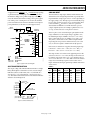
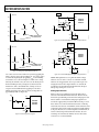
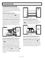
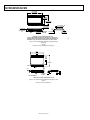
Figure 22 shows the power vs. throughput rate for automatic
full power-down.
VDD
PD
tPOWER-UP
100
tPOWER-UP
1µs
1µs
CONVST
10
CONVERSION
INITIATED HERE
POWER (mW)
CONVERSION
INITIATED HERE
ON-CHIP REFERENCE
VDD
1
tPOWER-UP
tPOWER-UP
25µs
25µs
CONVST
CONVERSION
INITIATED HERE
01321-020
0
CONVERSION
INITIATED HERE
0
50
100
150 200 250 300 350
THROUGHPUT (kSPS)
400
450
500
01321-023
0.1
PD
Figure 22. AD7822/AD7825/AD7829 Power vs. Throughput
Figure 20. AD7822/AD7825 Power-Up Time
0
POWER VS. THROUGHPUT
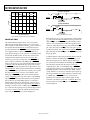
2048 POINT FFT
SAMPLING
2MSPS
fIN = 200kHz
–10
Superior power performance can be achieved by using the
automatic power-down (Mode 2) at the end of a conversion
(see the Operating Modes section).
–20
(dB)
–30
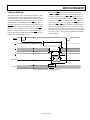
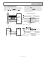
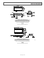
Figure 21 shows how the automatic power-down is implemented
using the CONVST signal to achieve the optimum power
performance for the AD7822/AD7825/AD7829. The duration
of the CONVST pulse is set to be equal to or less than the power-up
time of the devices (see the Operating Modes section). As the
throughput rate is reduced, the device remains in its powerdown state longer and the average power consumption over time
drops accordingly.
–40
–50
–60
FREQUENCY (kHz)
01321-024
–80
0
28
57
85
113
142
170
198
227
255
283
312
340
368
396
425
453
481
510
538
566
595
623
651
680
708
736
765
793
821
850
878
906
935
963
991
–70
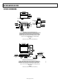
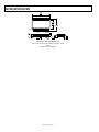
Figure 23. AD7822/AD7825/AD7829 SNR
tPOWER-UP tCONVERT
1µs
330ns
OPERATING MODES
POWER-DOWN
01321-022
CONVST
tCYCLE
10µs @ 100kSPS
Figure 21. Automatic Power-Down
For example, if the AD7822 is operated in a continuous
sampling mode, with a throughput rate of 100 kSPS and using
an external reference, the power consumption is calculated as
follows. The power dissipation during normal operation is
36 mW, VDD = 3 V. If the power-up time is 1 μs and the conversion
time is 330 ns (@ +25°C), the AD7822 can be said to dissipate
36 mW (maximum) for 1.33 μs during each conversion cycle.
If the throughput rate is 100 kSPS, the cycle time is 10 μs and
the average power dissipated during each cycle is (1.33/10) ×
(36 mW) = 4.79 mW. This calculation uses the minimum
conversion time, thus giving the best-case power dissipation at
this throughput rate. However, the actual power dissipated
during each conversion cycle could increase, depending on the
actual conversion time (up to a maximum of 420 ns).
The AD7822/AD7825/AD7829 have two possible modes of
operation, depending on the state of the CONVST pulse
approximately 100 ns after the end of a conversion, that is, upon
the rising edge of the EOC pulse.
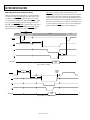
Mode 1 Operation (High Speed Sampling)
When the AD7822/AD7825/AD7829 are operated in Mode 1,
they are not powered down between conversions. This mode of
operation allows high throughput rates to be achieved.
Figure 24 shows how this optimum throughput rate is achieved
by bringing CONVST high before the end of a conversion, that
is, before the EOC pulses low. When operating in this mode, a
new conversion should not be initiated until 30 ns after the end
of a read operation. This allows the track-and-hold to acquire
the analog signal to 0.5 LSB accuracy.
Rev. C | Page 15 of 28