1
AD7822/AD7825/AD7829
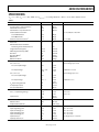
SPECIFICATIONS
VDD = 3 V ± 10%, VDD = 5 V ± 10%, GND = 0 V, VREF IN/OUT = 2.5 V. All specifications −40°C to +85°C, unless otherwise noted.
Table 1.
Parameter
DYNAMIC PERFORMANCE
Signal to (Noise + Distortion) Ratio 1
Total Harmonic Distortion1
Peak Harmonic or Spurious Noise1
Intermodulation Distortion1
Second-Order Terms
Third-Order Terms
Channel-to-Channel Isolation1
DC ACCURACY
Resolution
Minimum Resolution for Which
No Missing Codes Are Guaranteed
Integral Nonlinearity (INL)1
Differential Nonlinearity (DNL)1
Gain Error1
Gain Error Match1
Offset Error1
Offset Error Match1
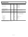
ANALOG INPUTS 2
VDD = 5 V ± 10%
VIN1 to VIN8 Input Voltage
VMID Input Voltage
VDD = 3 V ± 10%
VIN1 to VIN8 Input Voltage
VMID Input Voltage
VIN Input Leakage Current
VIN Input Capacitance
VMID Input Impedance
REFERENCE INPUT
VREF IN/OUT Input Voltage Range
Input Current
ON-CHIP REFERENCE
Reference Error
Temperature Coefficient
LOGIC INPUTS
Input High Voltage, VINH
Input Low Voltage, VINL
Input High Voltage, VINH
Input Low Voltage, VINL
Input Current, IIN
Input Capacitance, CIN
Version B
Unit
48
−55
−55
dB min
dB max
dB max
−65
−65
−70
dB typ
dB typ
dB typ
8
Bits
8
±0.75
±0.75
±2
±0.1
±1
±0.1
Bits
LSB max
LSB max
LSB max
LSB typ
LSB max
LSB typ
Test Condition/Comment
fIN = 30 kHz, fSAMPLE = 2 MHz
fa = 27.3 kHz, fb = 28.3 kHz
fIN = 20 kHz
See Analog Input section
Input voltage span = 2.5 V
VDD
0
VDD − 1.25
1.25
V max
V min
V max
V min
VDD
0
VDD − 1
1
±1
15
6
V max
V min
V max
V min
μA max
pF max
kΩ typ
2.55
2.45
1
100
V max
V min
μA typ
μA max
±50
50
mV max
ppm/°C typ
2.4
0.8
2
0.4
±1
10
V min
V max
V min
V max
μA max
pF max
Default VMID = 1.25 V
Input voltage span = 2 V
Default VMID = 1 V
2.5 V + 2%
2.5 V − 2%
Nominal 2.5 V
Rev. C | Page 3 of 28
VDD = 5 V ± 10%
VDD = 5 V ± 10%
VDD = 3 V ± 10%
VDD = 3 V ± 10%
10 nA typical, VIN = 0 V to VDD