1
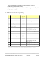
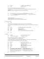
Register 50h, 54h, 58h, 5ch of Device 14h, Function 3
Field Name
Base Address
Bits
31:11
Length
10:2
Read Protect
1
Write Protect
0
Description
ROM Base address. The most significant 21 bits of the base address are
defined in this field. Bits 10:0 of the base address are assumed to be zero.
Base address, therefore, is aligned at a 2K boundary.
These 9 bits (0-511) define the length from 1K to 512K in increments of
1K.
When set, the memory range defined by this register is read protected.
Reading any location in the range returns FFh.
When set, the memory range defined by this register is write protected.
Writing to the range has no effect.
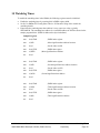
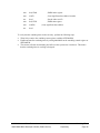
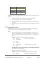
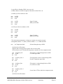
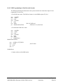
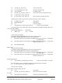
Example:
Protect 32K LPC ROM starting with base address FFF80000.
Base address bits 31:11
1111 1111 1111 1000 0000 0 b
Length 32K bit 10:2 = 31h = 000 0111 11 b
Read protect bit 1 = 1
Write protect bit 0 = 1
Register 50h = 1111 1111 1111 1000 0000 0000 0111 1111 b = FFF8007F h
Note:
1. Registers 50h ~ 5Fh can be written once after the hardware reset. Subsequent writes to them
have no effect.
2. Setting sections of the LPC ROM to either read or write protect will not allow the ROM to be
updated by a flash programming utility. Most flash utilities write and verify ROM sectors,
and will terminate programming if verification fails due to read protect.
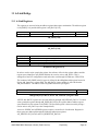
3.1.4
SPI ROM controller
The SPI ROM interface is a new feature added to the SB600. Refer to the AMD SB600 Register Reference
Guide for more information on this feature.
Note: The LPC ROM Read/Write Protect mentioned in the previous paragraph also applies to SPI. Two
strap pins, PCICLK0 and PCICLK1, determine the SB600 boot up from LPC ROM or SPI ROM. There is
no register status to reflect whether the current ROM interface is LPC or SPI.
© 2008 Advanced Micro Devices Inc.
AMD SB600 BIOS Developer’s Guide (Public Version)
SB600 Early-POST Initialization
Proprietary
Page 16