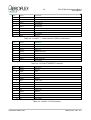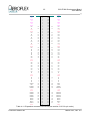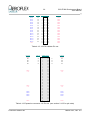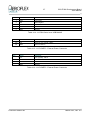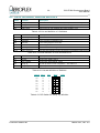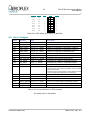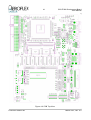
1
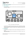
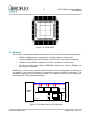
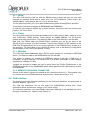
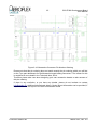
GR-UT699
Development Board
User Manual
AEROFLEX GAISLER AB
Rev. 0.6, 2013-03-28
2
GR-UT699 Development Board
User Manual
Information furnished by Aeroflex Gaisler AB is believed to be accurate and reliable.
However, no responsibility is assumed by Aeroflex Gaisler AB for its use, nor for any infringements
of patents or other rights of third parties which may result from its use.
No license is granted by implication or otherwise under any patent or patent rights of Aeroflex
Gaisler AB.
Aeroflex Gaisler AB
tel +46 31 7758650
Kungsgatan 12
fax +46 31 421407
411 19 Göteborg
[email protected]
Sweden
www.aeroflex.com/gaisler
Copyright © 2013 Aeroflex Gaisler
All information is provided as is. There is no warranty that it is correct or suitable for any purpose,
neither implicit nor explicit.
© Aeroflex Gaisler AB
March 2013, Rev. 0.6
3
GR-UT699 Development Board
User Manual
TABLE OF CONTENTS
1
INTRODUCTION...........................................................................................................7
1.1
1.2
1.3
1.4
2
Overview...................................................................................................................... 7
References...................................................................................................................9
Handling....................................................................................................................... 9
Abbreviations............................................................................................................. 10
ELECTRICAL DESIGN...............................................................................................11
2.1
2.2
2.3
2.3.1
2.3.2
2.3.3
2.3.4
2.4
2.4.1
2.4.2
2.5
2.5.1
2.5.2
2.6
2.7
2.8
2.8.1
2.8.2
2.8.3
2.8.4
2.9
2.10
2.11
2.11.1
2.11.2
2.12
2.12.1
2.12.2
2.12.3
2.12.4
2.12.5
Block Diagram............................................................................................................ 11
UT699 ASIC............................................................................................................... 11
Memory...................................................................................................................... 12
SRAM......................................................................................................................... 13
FLASH....................................................................................................................... 13
EEPROM.................................................................................................................... 13
MEMORY EXPANSION CONNECTOR.....................................................................13
CAN Interface............................................................................................................ 14
Configuration of Bus Termination...............................................................................14
Configuration of Slew Rate.........................................................................................15
Spacewire (LVDS) Interfaces.....................................................................................15
SPW interface circuit..................................................................................................15
SPWCLK.................................................................................................................... 16
Serial Interface........................................................................................................... 17
Debug Support Unit (DSU) Serial Interface................................................................17
Oscillators and Clock Inputs.......................................................................................19
System Clock............................................................................................................. 19
SPW_CLK.................................................................................................................. 19
Ethernet Clock............................................................................................................ 19
PCI Clock................................................................................................................... 20
Power Supply and Voltage Regulation......................................................................20
Ethernet Interface......................................................................................................20
PCI Interface.............................................................................................................. 21
Host/System Slot Configuration.................................................................................22
Peripheral Slot Configuration.....................................................................................23
Other Interfaces and Circuits.....................................................................................24
GPIO.......................................................................................................................... 24
Reset Circuit and Button............................................................................................24
Watchdog................................................................................................................... 25
JTAG interface........................................................................................................... 25
Mezzanine/Memory Expansion...................................................................................25
3
SETTING UP AND USING THE BOARD...................................................................27
4
INTERFACES AND CONFIGURATION.....................................................................32
4.1
4.2
4.3
List of Front/Back Panel Connectors..........................................................................32
List of Oscillators, Switches and LED's......................................................................42
List of Jumpers........................................................................................................... 43
© Aeroflex Gaisler AB
March 2013, Rev. 0.6
4
GR-UT699 Development Board
User Manual
LIST OF TABLES
Table 3-1: Default Status of Jumpers/Switches..............................................................................27
Table 4-1: List of Connectors......................................................................................................... 32
Table 4-2: J1 UART-1 - Serial Interface (RS232) connections .....................................................34
Table 4-3: J2 RJ45-ETHERNET Connector...................................................................................34
Table 4-4: J3 ASIC– JTAG Connector ..........................................................................................34
Table 4-5: J4A (upper connector) CANBUS-1 interface connections............................................35
Table 4-6: J4B (lower connector) CANBUS-0 interface connections..............................................35
Table 4-7: J5 SPW-0 interface connections .................................................................................35
Table 4-8: J6 SPW-1 interface connections .................................................................................36
Table 4-9: J7 SPW-2 interface connections .................................................................................36
Table 4-10: J8 SPW-3 interface connections................................................................................36
Table 4-11: Expansion connector J9 Pin-out (see section 2.12.5 for pin order).............................38
Table 4-12: J10 PIO Header Pin out..............................................................................................38
Table 4-13: Expansion connector J11 Pin-out (see section 2.12.5 for pin order)..........................39
Table 4-14: J12 DSU-Serial over USB MiniAB...............................................................................40
Table 4-15: J13 POWER – External Power Connector..................................................................40
Table 4-16: J14 POWER – External Power Connector..................................................................40
Table 4-17: SODIMM socket J15 Pin-out.......................................................................................42
Table 4-18: List and definition of Oscillators..................................................................................42
Table 4-19: List and definition of PCB mounted LED's...................................................................42
Table 4-20: List and definition of Switches.....................................................................................42
Table 4-21: DIP Switch S3 'PIO[7..0]' definition.............................................................................42
Table 4-22: DIP Switch S4 'PIO[15..8]' definition............................................................................43
Table 4-23: List and definition of PCB Jumpers.............................................................................43
© Aeroflex Gaisler AB
March 2013, Rev. 0.6
5
GR-UT699 Development Board
User Manual
LIST OF FIGURES
Figure 1-1: GR-UT699 Development Board.....................................................................................8
Figure 2-1: Block Diagram of GR-UT699 board.............................................................................11
Figure 2-2: UT699 ASIC................................................................................................................. 12
Figure 2-3: On-Board Memory Configuration.................................................................................13
Figure 2-4: Block Diagram of the CAN interface............................................................................14
Figure 2-5: Transceiver and Termination Configuration (one of 2 interfaces shown).....................15
Figure 2-6: Transceiver and Termination of the SPW interfaces (2 of 4 interfaces shown)............16
Figure 2-7: Serial interface............................................................................................................. 17
Figure 2-8: Debug Support Unit connections.................................................................................17
Figure 2-9: Clock Distribution Scheme...........................................................................................19
Figure 2-10: Power Regulation Configuration.................................................................................20
Figure 2-11: Block diagram of Ethernet Interface...........................................................................21
Figure 2-12: Block diagram for PCI System Slot connections........................................................22
Figure 2-13: Block diagram of PCI Peripheral connections............................................................23
Figure 2-14: PIO interface.............................................................................................................. 24
Figure 2-15: Watchdog configuration.............................................................................................25
Figure 2-16: Mezzanine Connector Pin Number Ordering..............................................................26
Figure 3-1: GRMON Output Screenshot #1...................................................................................29
Figure 3-2: GRMON Output Screenshot #2...................................................................................31
Figure 4-1: Front Panel View (pin 1 of connectors marked)...........................................................33
Figure 4-2: PCB Top View.............................................................................................................. 44
Figure 4-3: GR-UT699 Assembly Photo.........................................................................................45
REVISION HISTORY
Revision
Date
0.1 DRAFT
2008-05-01 All
New document/draft
0.2
2008-09-16 §2.5.2
§2.12.1
18
41
Added note about SPWCLK oscillator
Added notes about PCI_INT[A B C D] signals
Modified Figure 2-9
Updated Figure 4-2.
0.3
2008-10-27 All
Formatting changes
0.4
2009-01-07 7,28,29,
41,42
Updated Figure 1-1, Figure 3-1, Figure 3-2, Figure 4-2, Figure 4-3
0.5
2012-12-10 §1.2
§2.3.4
§2.12.15
Added a link to reference document about Mezzanine Connectors
Added description of Mezzanine connectors and pin numbering
0.6
2013-03-28 §2.11.1,
§2.11.2
§3
Corrected references to JP8 / JP10 in PCI jumper configurations
© Aeroflex Gaisler AB
Page
Description
Added paragraph explaining grmon command for using Digilent HS-1 JTAG
cable.
March 2013, Rev. 0.6
6
GR-UT699 Development Board
User Manual
Intentionally Blank
© Aeroflex Gaisler AB
March 2013, Rev. 0.6
7
1
GR-UT699 Development Board
User Manual
INTRODUCTION
1.1 Overview
This document describes the GR-UT699 Development Board.
The purpose of this equipment is to provide developers with a convenient hardware platform
for the evaluation and development of software for the Aeroflex UT699RH RadHard 32-bit
Fault-Tolerant LEON 3FT/SPARCTM V8 Processor ASIC device. The UT699 is a Leon3FT
based custom ASIC for Aerospace applications.
The GR-UT699 Unit comprises a custom designed PCB with a 6U Compact PCI front panel,
making the board suitable either for stand-alone bench top development, or for installation in
a 6U High Compact PCI rack. All the principle interfaces and functions are accessible on
front panel connectors.
Figure 1-1: GR-UT699 Development Board
The interface connectors on the Front Panel of the unit provide:
© Aeroflex Gaisler AB
March 2013, Rev. 0.6
8
•
•
•
•
•
•
•
•
•
GR-UT699 Development Board
User Manual
One Serial UART interface (RS232)
Ethernet
JTAG - DSU
Two CAN bus interfaces
Four Spacewire interfaces
Serial DSU UART (Mini-AB USB connector)
16 pins General Purpose I/O Port
Push Buttons for RESET and BREAK
LED indicators
To enable convenient connection to the interfaces, the connector types and pin-outs are
compatible with the standard connector types for these types of interfaces.
Additionally the board is equipped with a 32 bit Master/target PCI interface via standard
Compact PCI Connector interface on the back edge of the PCB.
The PCB contains the following main items as detailed in section 2 of this document:
•
UT699RH ASIC
•
Memory
• SRAM
•
•
•
•
80 Mbit
(1 banks x 2Mword x 40 bit, typ. 10ns)
(optional second bank is not fitted as standard)
SDRAM SODIMM socket
(up to 64Mword x 40 bit with 512Mbyte module)
FLASH
128Mbit
(4M x 32 bit, typ. 90ns)
EEPROM DIL32 socket
(1 bank x 1Mbit, organised x8 bit wide)
additional memory via memory expansion connector
•
Interfaces
• two CAN interfaces
• four Spacewire LVDS electrical interfaces
• one serial UART (RS232) interface
• 10/100MBit Ethernet PHY
• DSU - Serial (over USB Converter) interface
• DSU - JTAG (over JTAG connector) interface
• GPIO (16 signals) general purpose input/output port
•
Power, Reset, Clock and Auxiliary circuits
1.2 References
RD-1
GR-UT699_schematic.pdf, Schematic
RD-2
GR-UT699_assy_drawing.pdf, Assembly Drawing
RD-3
UT699RH Datasheet
RD-4
GR-MEZZ Technical Note, Technical Note about Mezzanine connectors
© Aeroflex Gaisler AB
March 2013, Rev. 0.6
9
GR-UT699 Development Board
User Manual
1.3 Handling
ATTENTION : OBSERVE PRECAUTIONS FOR
HANDLING ELECTROSTATIC SENSITIVE DEVICES
This unit contains sensitive electronic components which can be damaged by Electrostatic
Discharges (ESD). When handling or installing the unit observe appropriate precautions and
ESD safe practices.
When not in use, store the unit in an electrostatic protective container or bag.
When configuring the jumpers on the board, or connecting/disconnecting cables, ensure that
the unit is in an unpowered state.
1.4 Abbreviations
DIL
ESD
FP
FT
GPIO
I/O
IP
LVDS
MII
MUX
PCB
SPW
Dual In-Line
Electro-Static Discharge
Front Panel
Fault-Tolerant
General Purpose Input / Output
Input/Output
Intellectual Property
Low Voltage Digital Signalling
Media Independent Interface
Multiplexer
Printed Circuit Board
Spacewire
© Aeroflex Gaisler AB
March 2013, Rev. 0.6
10
2
GR-UT699 Development Board
User Manual
ELECTRICAL DESIGN
2.1 Block Diagram
The GR-UT699 board provides the electrical functions and interfaces as represented in the
block diagram, Figure 2-1.
POWER
COMPACT PCI
INTERFACE
UT699RH
ASIC
FLASH
EEPROM
SDRAM
SRAM
MEMORY
EXPANSION
POWER
&
AUX
DIP
SWITCHES
GPIO I/F
SERIAL
DSU
CANBUS
16 x GPIO
USBSERIAL
2 x CAN
SPW
ETHERNET PHY
UART
RS232
4 x SPW
10/100 Mb
ETHERNET
1 x RS232
UART
Figure 2-1: Block Diagram of GR-UT699 board
The Main PCB is of standard Double Eurocard format (233.35 x 160mm) and, in principle,
could be used 'stand-alone' on the bench-top simply using an external +5V power supply.
The board is fitted with a Compact PCI front panel, and is compatible with mounting in a 6U
Compact PCI rack.
2.2 UT699 ASIC
The UT699RH ASCI is packaged in a 352-pin Ceramic Quad Flatpack, and is soldered in to
the PCB.
Details of the interfaces, operation and programming of the UT699 ASIC is given in the
UT699 Datasheet, RD-3.
© Aeroflex Gaisler AB
March 2013, Rev. 0.6
11
GR-UT699 Development Board
User Manual
Figure 2-2: UT699 ASIC
2.3 Memory
The memory configuration installed on the board is shown in the figure below comprising of:
•
80Mbit of SRAM memory, organised as 1 banks x 2Mword x 40 bits wide
(a second SRAM bank can be installed on the PCB, but is not fitted as standard)
•
128Mbit of Flash PROM, organised as 1 bank x 4 Mword x 32 bits wide)
•
DIL 32 pin socket to allow 1Mbit of EEPROM organised as 1 bank x 128kByte x 8
bits wide) to be installed
ADDR
DATA
32
FLASH
FLASH
8
EEPROM
EEPROM
UT699RH
UT699RH
ASIC
ASIC
(32+8)
SRAM
SRAM
SRAM
SRAM
SRAM
SRAM
BANK0
RAMSN0
BANK1
RAMSN1
CONTROL
ROMSN0
SRAM
SRAM
SRAM
SRAM
SRAM
SRAM
MEMORY EXPANSION CONNECTOR
Additionally, in order to allow users to install alternative memory configurations or devices, all
the signals of the memory interface are connected to memory expansion connectors. The
expansion connectors allow mezzanine boards to be added similar to those developed for
the existing GR-CPCI development boards.
Figure 2-3: On-Board Memory Configuration
© Aeroflex Gaisler AB
March 2013, Rev. 0.6
12
GR-UT699 Development Board
User Manual
2.3.1 SRAM
The GR-UT699 board is laid out with two SRAM memory banks but only has one bank
mounted as standard. Each bank is made up of five CY7C1069AV33. These devices are
16Mbit (2Mbyte x 8 bit devices with 10 or 12 ns access times.
The five devices provide (32 + 8) bit wide SRAM memory paths allowing EDAC operation.
These memory banks are mapped as RAMBANK0 and RAMBANK1.
In case the user wishes to disable the on board memory, this can be done by removing the
jumpers JP5 on the PCB.
2.3.2 FLASH
The GR-UT699 board has mounted as standard one FLASH memory bank, made up of two
Intel JS28F640J3 FLASH devices. These devices are 64Mbit (8Mbyte x 16 bit devices),
typically with 90ns access times. The data bus width to the Flash memory is 32 bits wide.
Note that, the PROM width and PROM EDAC conditions are set by the state of the
GPIO[2..0] pins at power up of the Processor. Therefore the GPIO[2..0] DIP switches on the
PCB must be appropriately set for the correct operation of the PROM memory at start up of
the processor. For information on the GPIO[2..0] settings refer to the Memory Configuration
documentation in the Leon3 User Manual, or RD-3.
2.3.3 EEPROM
The GR-UT699 board additionally has a DIP32 socket suitable for mounting an EEPROM
device. The data bus width to the EEPROM device is 8 bits wide.
This socket is suitable for mounting an EEPROM device of the type AT28LV010, or
compatible, in DIP32 package. The AT28LV010 is an ATMEL EEPROM, of 1Mbit capacity
organised as 128kByte x 8 bits.
Jumpers are provided to enable the user to select either the FLASH PROM device or the
EEPROM to operate as the ROMBANK0 device which appears at the initial memory location
of 0x00000000.
2.3.4 MEMORY EXPANSION CONNECTOR
Access to the memory signals is provided by the connectors J9 and J11. This enables uses
to conceive their own mezzanine boards and functions. Please see section.2.12.5
2.4 CAN Interface
The board provides the electrical interfaces for two CAN bus interfaces, as represented in
the block diagram, Figure 2-4.
The CAN bus transceiver IC's on this board are SN65HVD230 devices from Texas
Instruments which operate from a single +3.3V power supply.
The connector interfaces are male DSUB-9 connectors adhering to the standard pin-out for
this type of interface (ref. Table 4-6 And Table 4-5).
© Aeroflex Gaisler AB
March 2013, Rev. 0.6
13
CAN
CAN
TRANSCEIVER
TRANSCEIVER
TXD
RXD
CAN_L
CAN_H
CAN
CAN
TRANSCEIVER
TRANSCEIVER
CAN_L
CAN
interface 2
CONTROLLER LOGIC IN ASIC
RXD
CAN_H
CAN
interface 1
TXD
GR-UT699 Development Board
User Manual
Figure 2-4: Block Diagram of the CAN interface
2.4.1 Configuration of Bus Termination
The CAN interfaces on the board can be configured for either end node or stub-node
operation by means of the jumpers JP3 and JP4 for interface 1 and 2 respectively, as shown
in Figure 2-5.
For normal end-node termination with a nominal 120 Ohm insert jumpers in position 1-3.
However, if a split termination is desired (if required for improved EMC performance), insert
the jumpers in positions 1-2 and 3-4.
For stub nodes, if termination is not required, do not install any jumpers.
© Aeroflex Gaisler AB
March 2013, Rev. 0.6
14
GR-UT699 Development Board
User Manual
Figure 2-5: Transceiver and Termination Configuration (one of 2 interfaces shown)
2.4.2 Configuration of Slew Rate
The SN65HVD230 transceiver device used on the board has the facility to set the device into
STANDBY mode, by connecting an active high external signal to pin 8 of the device (refer to
the device data sheet). However, on this board this is tied to permanently 'low' to enable the
CAN bus Transceivers.
A further feature provided by the SN65HVD230 device is the capability to adjust the
transceiver slew rate. This can be done by modifying the values of resistors connected to pin
8 of the transceivers.
The default value of 0 ohms is compatible with 1Mbps operation.
From the data sheet the following resistor values give the following slew rates:
10kOhm => 15V/us
100kOhm => 2V/us
2.5 Spacewire (LVDS) Interfaces
The UT699 ASIC provides four Spacewire interfaces which are routed to the front panel of
the board.
2.5.1 SPW interface circuit
Each Spacewire interface consists of 4 LVDS differential pairs (2 input pairs and 2 output
pairs), as shown in the figure below. As the Spacewire interface to the UT699 ASIC is
LVTTL (3.3V logic), LVDS driver and receiver circuits are required on the PCB to interface
between the ASIC and the external interface.
The PCB traces for the LVDS signals on the GR-UT699 board are laid out with 100-Ohm
differential impedance design rules and matched trace lengths.
100 Ohm Termination resistors for the LVDS receiver signals are mounted on the board
close to the receiver.
© Aeroflex Gaisler AB
March 2013, Rev. 0.6
15
GR-UT699 Development Board
User Manual
The pin out and connector types for these Spacewire interfaces conform to the Spacewire
standard, as shown in Figure 2-6.
The inner shield pin (pin3 of the connector) is connected to DGND via a Zero-ohm resistor.
2.5.2 SPWCLK
Configuration options on the board (jumpers, crystal socket and SMA coaxial connector)
allow this Spacewire clock to be provided from the following sources:
•
Dedicated SPWCLK oscillator (if appropriate Oscillator X3 is mounted in socket and
jumper J17 is not installed)
•
Main processor oscillator X1(if jumper J17 is installed)
•
External clock input via SMA connector J16. (X3 and J17 not installed)
The default configuration is that the clock is supplied by the SPWCLK oscillator X3, and
Figure 2-6: Transceiver and Termination of the SPW interfaces (2 of 4 interfaces shown)
jumper J17 is not installed. Do not install jumper J17 if an oscillator is installed in X3 socket
as this will unintentionally connect the outputs of oscillator X1 and Oscillator X3 together.
© Aeroflex Gaisler AB
March 2013, Rev. 0.6
16
GR-UT699 Development Board
User Manual
2.6 Serial Interface
The UT699RH ASIC, provides a single Serial port, with TXD/RXD pins, and the GR-UT699
board provides an RS232 driver/receiver chip and routes these signals to a front panel
connector.
The front panel connector type for the UART interface is Female D-Sub 9 pin type with a
standard pin-out for serial links.
SUB-D 9 pin
Female
TXD
UT699RH
ASIC
RS232
DRIVER/
RECEIVERS
RS232
INTERFACE
RXD
Figure 2-7: Serial interface
2.7 Debug Support Unit (DSU) Serial Interface
The GR-UT699 unit provides a interface for Debug and control of the processor by means of
a host terminal via the DSU serial link to the UT699 ASIC, as represented in Figure 2-8.
JTAG
USB-SERIAL
HOST
TERMINAL/COMPUTER
USB to SERIAL
CONVERTER
DSUBRE→
DSUACT←
DSU I/F
DSUTX←
DSURX→
UT699RH
ASIC
DSUEN→
Figure 2-8: Debug Support Unit connections
The board provides two possibilities for connecting to the processor's DSU interface:
1. USB MiniAB connector with USB to Serial interface chip
2. JTAG DSU interface
The baud rate of the serial link is specified by the host computer, and the DSU interface in
the UT699 ASIC auto-detects and adjusts its baud rate to suit.
The DSUENable signal input to the processor is connected to a jumper on the PCB. In
© Aeroflex Gaisler AB
March 2013, Rev. 0.6
17
GR-UT699 Development Board
User Manual
normal use the DSU feature will always be enabled to allow processor control and program
debugging via the DSU link.
An LED is provided on the PCB to indicate the conditions of the DSUACT signal from the
UT699 processor. Additionally connections are provided to an LED indicator on the front
panel of the Unit.
A miniature push button switch is provided on the Main PCB for the DSUBREAK control, and
connections are provided to an additional push-button switch on the front panel of the unit.
© Aeroflex Gaisler AB
March 2013, Rev. 0.6
18
GR-UT699 Development Board
User Manual
2.8 Oscillators and Clock Inputs
The oscillator and clock scheme for the UT699 ASIC is shown in Figure 2-9.
MEMORY
MEMORYEXPANSION
EXPANSION
CONNECTOR
CONNECTOR
COAX CONNECTOR
ZERO
ZERO
DELAY
DELAY
BUFFER
BUFFER
TBD
TBDMHz
MHz
SYS CLK
DIL8 SOCKET
UT699RH
ASIC
COAX CONNECTOR
SDCLK
SDRAM
SDRAM
MODULE
MODULE
SPW CLK
TBD
TBDMHz
MHz
DIL8 SOCKET
Ethernet
Ethernet
PHY
PHY
25
25MHz
MHz
ETH_TXCLK
ETH_RXCLK
SMD
ZERO
ZERO
DELAY
DELAY
BUFFER
BUFFER
33.3
33.3MHz
MHz
PCI_CLK
SMD
PCI Backplane
Figure 2-9: Clock Distribution Scheme
2.8.1 System Clock
The main oscillator for the UT699 ASIC is a 75 MHz Crystal oscillator. This oscillator will be
a 4 pin DIL8 style oscillator, installed in a socket on the board. A zero-delay buffer circuit
(CY2305) is used to distribute the SYSCLK.
2.8.2 SPW_CLK
The SPWCLK can be derived from either the SYSCLK, a separate socketed on-board crystal
oscillator, or can be injected on a coaxial connector on the board.
2.8.3 Ethernet Clock
A dedicated 25MHz SMD oscillator is provided for the Ethernet Controller and PHY circuit
(see section 2.10).
2.8.4 PCI Clock
A dedicated 33.3MHz SMD oscillator and zero delay buffer are provided for the PCI clock.
For information on the configuration, please see section 2.11.
© Aeroflex Gaisler AB
March 2013, Rev. 0.6
19
GR-UT699 Development Board
User Manual
2.9 Power Supply and Voltage Regulation
The board operates from a single +5V DC power supply input. On board regulators generate
the following voltages:
+3.3V for the UT699 I/O voltage, memory chip and other peripherals
•
+2.5V for UT699 Vcore voltage
REGULATOR
JP14
Vcore
(+2.5V for UT699RH core)
REGULATOR
JP13
1
JP15
+3V3asic
(+3.3V for UT699RH)
2
JP12
+3.3V
3
CPCI CONNECTOR
•
+5V PCI
1
+3.3V PCI
2
3
n.c.
EXTERNAL POWER
SUPPLY, REGULATED
+5V, >1A
±12V PCI
J13 POWER
2.1mm JACK
+VIO PCI
MEZZ. CONN.
Figure 2-10: Power Regulation Configuration
All voltages +5V, +3.3V, ±12V are provided via the memory expansion connector interface
making feasible that user defined mezzanine boards can use these voltages.
If the Board is installed in a Compact PCI rack, the board can be configured by means of
jumpers such that the +5V, +3.3V, +12V and -12V are provided from the Compact PCI
backplane instead of the internal regulators.
2.10 Ethernet Interface
The UT699RH ASIC device incorporates a Ethernet controller with support for MII interface,
and the GR-UT699 Development Board has an Intel LXT971 10/100Mbit/s Ethernet PHY
transceiver and RJ45 connector are on board.
For more information on the registers and functionality of the Ethernet MAC+PHY device
please refer to the data sheet for the WJLXT971A device.
A 25MHz oscillator dedicated for this device is provided on the board.
The interrupt output of the Ethernet MDIO interface is connected to the PIO[4] input to the
UT699 ASIC. This can be disabled by removing jumper JP2 if necessary.
© Aeroflex Gaisler AB
March 2013, Rev. 0.6
20
4
ETH_RXD[3..0]
4
ETH_TXD[3..0]
GR-UT699 Development Board
User Manual
ETH_RXERR
ETH_RXDV
ETH_TXER
RJ45
ETH_TXEN
ETH_CRS
ETH_COL
UT699RH
ETHERNET
PHY
ETH_MDIO
ETH_MDC
ETH_MDINT
ETH_CLK
ETH_RXCLK
25MHz
ETH_TXCLK
Figure 2-11: Block diagram of Ethernet Interface
2.11 PCI Interface
The UT699RH ASIC incorporates a 33MHz/32 bit interface with 8 channel PCI Arbiter and is
capable of being configured to be installed in either the SYSTEM slot (HOST) or in
PERIPHERAL slots (GUEST).
The GR-UT699 board can be configured to operate either as a peripheral slot card or system
slot card as described in the following sections.
Note that the GR-UT699 board has been designed to operate in a 3.3V signalling
environment, and the Compact PCI connector is appropriately keyed (yellow key).
© Aeroflex Gaisler AB
March 2013, Rev. 0.6
21
GR-UT699 Development Board
User Manual
2.11.1 Host/System Slot Configuration
When installed in the System slot, the board provides the PCI arbitration and distributes the
required PCI clocks to the backplane, and to the PCI interface in the FPGA.
ASIC
SYSEN
HOST
IDSEL
IDSEL
GND
ARBITER
REQ
GNT
REQ7
REQ6
REQ5
REQ4
REQ3
REQ2
REQ1
REQ0
JP9
4 3 2 1
GNT7
GNT6
GNT5
GNT4
GNT3
GNT2
GNT1
GNT0
JP10
4 3 2 1
PCICLKIN
1
3
2
4
JP7
BUFFER
REQ6N
REQ5N
REQ4N
REQ3N
REQ2N
REQ1N
REQN
GNT6N
GNT5N
GNT4N
GNT3N
GNT2N
GNT1N
GNTN
PCICLK
PCICLK1
PCICLK2
PCICLK3
PCICLK4
PCICLK5
PCICLK6
CPCI EDGE CONNECTOR
XTAL
33MHz
Figure 2-12: Block diagram for PCI System Slot connections
This requires the jumpers to be installed as follows:
JP7
1-2 and 3-4
JP9
1-2 and 3-4
JP10
1-2 and 3-4
Additionally, the PCI specification requires that the following system signals are pulled-up by
the card operating in the system slot:
PCI_FRAMEN
PCI_IRDYN
PCI_TRDYN
PCI_DEVSELN
PCI_STOPN
PCI_PERRN
PCI_SERRN
PCI_LOCKN
This can be achieved by installing the JP8 jumpers 1-2, 3-4, 5-6, 7-8, 9-10, 11-12, 13-14, 1516, 17-18 and 19-20.
In order to ensure that the PCIRSTN pin on the back plane is not left floating, it is also
© Aeroflex Gaisler AB
March 2013, Rev. 0.6
22
GR-UT699 Development Board
User Manual
necessary to ensure that this pin is driven by the host slot. This can be achieved by installing
jumper JP18 on the board, so that the board system reset signal RESETN provides the drive
for the PCIRSTN signal. If the jumper is not installed, a weak (22k) pull up will pull the
PCIRSTN signal high.
2.11.2 Peripheral Slot Configuration
When functioning in a Peripheral slot, the board receives its input clock from the backplane,
and connects its REQN/GNTN signals to the backplane REQN/GNTN signals.
ASIC
HOST
IDSEL
IDSEL
ARBITER
REQ
GNT
REQ7
REQ6
REQ5
REQ4
REQ3
REQ2
REQ1
REQ0
REQ6N
REQ5N
REQ4N
REQ3N
REQ2N
REQ1N
JP9
REQN
4 3 2 1
GNT7
GNT6
GNT5
GNT4
GNT3
GNT2
GNT1
GNT0
GNT6N
GNT5N
GNT4N
GNT3N
GNT2N
GNT1N
JP10
GNTN
4 3 2 1
PCICLKIN
1
3
2
4
PCICLK
PCICLK1
PCICLK2
PCICLK3
PCICLK4
PCICLK5
PCICLK6
JP7
BUFFER
CPCI EDGE CONNECTOR
XTAL
33MHz
Figure 2-13: Block diagram of PCI Peripheral connections
This requires the jumpers to be installed as follows:
JP7
1-3
JP9
2-3
JP10
2-3
The jumpers in JP8 and JP18 should be not be installed.
© Aeroflex Gaisler AB
March 2013, Rev. 0.6
23
GR-UT699 Development Board
User Manual
2.12 Other Interfaces and Circuits
2.12.1 GPIO
The 16 general Purpose Input Output signals of the ASIC (3.3V LVTTL voltage levels) are
connected to a set of 0.1” pitch pin header connector on the front panel thus allowing easy
access to these signals. A series protection resistor of 470 Ohm is included on each signal
at the front panel connector.
Weak pull ups (47k) are provided on each of the signals lines on the PCB and additionally a
set of DIP Switches allow the user convenient programming of the signal state when the
GPIO lines are configured as inputs. When programmed as outputs the DIP switches should
be left in the 'open' state.
PULL-UP
(x16)
UT699RH
ASIC
16
GPIO[15..0]
GPIO[15..0]
SERIES
(x16)
DIP-SW
(x16)
GPIO[11..8] =
PCI_INT[A B C D ]
PCB
SERIES
(x4)
Figure 2-14: PIO interface
Note that the GPIO[11..8] signals are also connected to the PCI Interrupt pins PCI_INT[A B
C D] on the PCI connector PCI-J1 via a 33R series resistor. This is intended in order to allow
the GPIO signals to generate or receive PCI interrupts from the backplane if desired.
If the board is installed in a CPCI rack, setting/resetting the GPIO[11..8] may therefore
cause unintended behaviour, by generating a generating PCI Interrupts on the back plane.
If this behaviour is not desired, disconnect the GPIO signals from the PCI interrupts on the
back plane by removing resistor pack R35.
2.12.2 Reset Circuit and Button
A standard Processor Power Supervisory circuit (TPS3705 or equivalent) is provided on the
Board to provide monitoring of the 3.3V power supply rail and to generate a clean reset
signal at power up of the Unit.
To provide a manual reset of the board, a miniature push button switch is provided on the
Main PCB for the control. Additionally connections are provided to an additional push-button
RESET switch on the front panel of the unit.
2.12.3 Watchdog
The UT699 ASIC includes a Watchdog timer function which can be used for the purpose of
© Aeroflex Gaisler AB
March 2013, Rev. 0.6
24
GR-UT699 Development Board
User Manual
generating a system reset in the event of a software malfunction or crash.
On this development board the WDOGN signal is connected as shown in the Figure 2-15 to
the Processor Supervisory circuit.
FRONT
PANEL
LED
RESETN
UT699RH
ASIC
BOARD
MOUNTED
LED
WDOGN
RSTIN_N
JUMPER
JP1D
7-8
POWER-ON
RESET
CIRCUIT
Figure 2-15: Watchdog configuration
To utilise the Watchdog feature, it is necessary to appropriately set-up and enable the
Watchdog timer. Please consult the UT699 data sheet (RD-3) for the correct register
locations and details.
Also, to allow the WDOGN signal to generate a system reset it is necessary to install the
Jumper JP1 pins 7-8 (see Figure 2-15).
For software development it is often convenient or necessary to disable the Watchdog
triggering in order to be able to easily debug without interference from the Watchdog
operation. In this case, the Jumper JP1 7-8 should be in the removed. When the watchdog
triggers, the Watchdog LED's will illuminate, but a system reset will not occur.
2.12.4 JTAG interface
A 14 pin connector on the front panel provides the possibility to connect to the JTAG signals
and JTAG chain of the UT699 ASIC.
This interface allows DSU Debug over the JTAG interface to be performed.
2.12.5 Mezzanine/Memory Expansion
Two connectors, J9 and J11, are provided on the board which give access to the memory
bus signals of the UT699 processor. The signals which are made available on these
connectors are listed in Table 4-11 and Table 4-13 respectively.
This can allow users to implement either memory expansion on a mezzanine, or by including
the appropriate decoding logic on the mezzanine board, to implement peripheral circuits
mapped in the address range of the I/O space of the UT699 processor.
Figure 2-16, shows the pin numbering scheme as implemented on the GR-UT699 Board.
© Aeroflex Gaisler AB
March 2013, Rev. 0.6
25
GR-UT699 Development Board
User Manual
Figure 2-16: Mezzanine Connector Pin Number Ordering
Please note that this pin ordering does not match exactly the pin ordering which you will find
on the Tyco part datasheets for the Mezzanine board mating connectors. The reason for this
is explained in more detail in the Technical Note, RD-4.
Therefore please take care when designing your own mezzanine boards to take account of
this pin ordering.
If there is any confusion, or you have any doubts, please do not hesitate to contact
[email protected]. Additional dimensional data or Gerber layout information can be provided, if
required to aid in the layout of the User's mezzanine board.
© Aeroflex Gaisler AB
March 2013, Rev. 0.6
26
3
GR-UT699 Development Board
User Manual
SETTING UP AND USING THE BOARD
The default status of the Jumpers on the boards is as shown in table Figure 3-1.
In this configuration the board is set up as a PCI Host. For the meaning of the various
jumpers, refer to Table 4-23 and RD 1.
Jumper
JP1
JP2
JP3
JP4
JP5
JP6
JP7
JP8
JP9
JP10
JP11
JP12
JP13
JP14
JP15
JP16
JP17
JP18
Jumper Setting
1-2 not installed
3-4 not installed
5-6 not installed
7-8 installed
Not installed
Comment
ASIC TEST mode pin not enabled
DSU is enabled
JTAG interface is enabled
Watchdog output can cause board reset
Ethernet MDIO interface interrupt is not
connected to GPIO4
Install 1-3
End-stub termination enabled – see section
2.4.1
Install 1-3
End-stub termination enabled – see section
2.4.1
Install 1-2, 3-4, 5-6, 7-8
Connects RAMSN0 and RAMSN1 to on
board SRAM banks
Install 1-2
Connects ROMSN0 to on board Flash
Prom
Install 1-2 and 3-4
PCI Host Mode clocks to backplane – see
section 2.11
Install 1-2, 3-4, 5-6, 7-8, 9-10,
PCI Host Mode- Pull ups enabled – see
11-12, 13-14, 15-16, 17-18, 19section 2.11
20
Install 1-2 and 3-4
PCI Host Mode – see section 2.11
Install 1-2 and 3-4
PCI Host Mode – see section 2.11
Installed
Connects to Front Panel LED indicators
Installed 1-2
See section 2.9
Installed 1-2
See section 2.9
Installed
Can be used as current measure point for
Vcore supply to ASIC
Installed
Can be used as current measure point for
3.3V supply to ASIC
Installed
Connected to Front Panel push buttons for
RESET and BREAK
Not installed
Oscillator X3 provides source for
SPW_CLK
Installed 1-2
Board RESETN also generated PCI_RSTN
for PCI Host
Table 3-1: Default Status of Jumpers/Switches
To operate the unit stand alone on the bench top, connect the +5V power supply to the
Power Socket at the back of the unit.
The front-panel POWER LED should be illuminated indicating that the +3.3V power is active.
Upon power on, the Processor will start executing instructions beginning at the memory
location 0x00000000, which is the start of the PROM. If the PROM is 'empty' or no valid
program is installed, the first executed instruction will be invalid, and the processor will halt
with an ERROR condition, with the ERROR LED illuminated.
Pressing the DSU-BREAK button should illuminate the DSUACT LED and halt the
processor.
© Aeroflex Gaisler AB
March 2013, Rev. 0.6
27
GR-UT699 Development Board
User Manual
To perform software download and debugging on the processor, a link from the Host
computer to the DSU interface of the board is necessary. A connection to the DSU of the
board can be made using a USB cable (Type-A to Mini-AB connectors) from the Host PC to
the USB-DSU connector on the front panel.
Note, to use the USB-DSU interface you need to install the FTDI Virtual Com driver on the
Host PC. This driver allows the USB connection to the board to be used as a 'virtual' serial
port, operating at baud rates up to 460800 Baud.
These drivers can be downloaded from the FTDI web site, (www.ftdichip.com/FTDrivers.htm)
and drivers for both Linux and Windows are available. Information for the installation of
these drivers can be found on the FTDI web site
To perform program download and software debugging on the hardware it is necessary to
use the Gaisler Research GRMON debugging software, installed on a host PC (as
represented in Figure 2-8).
Note that it is necessary to use the 'PRO' version of GRMON, as the UT699 ASIC
incorporates FT features. It is not possible to use evaluation version of GRMON with this
ASIC. Please refer to the GRMON documentation for the installation of the software on the
host PC (Linux or Windows), and for the installation of the associated hardware dongle.
Starting GRMON, with the command:
grmon -i
will establish a link to the DSU, and will initialise the processor registers and timers.
The default serial interface used by GRMON is /dev/ttyS0 (linux) or com1 (Windows).
To use a different serial interface, specify the command
grmon -i -uart /dev/comXX
(where XX is the number of the com port)
In the example shown in Figure 3-1 a connection is being made with GRMON over the USBSerial link, which in this instance is com63 on the host (Windows) PC.
The resulting response generated on the Host Computer is shown in Figure 3-1.
Typing the command flash will reported the detected Flash Prom memory configuration and
info sys will provide more information on the processors registers and internal cores as
shown in Figure 3-2.
Rather than using the Serial-DSU interface for debugging it is also fossible to instead use
the JTAG interface.
To connect via the JTAG_DSU interface using a Xilinx JTAG programming cable, start
GRMON with the command:
grmon -i -jtag -freq 66
(where '66' is is the clock frequency of the main processor oscillator).
Alternatively to connect via the JTAG_DSU interface using a Digilent HS-1 JTAG cable
(when running GRMON on MS-Windows), start GRMON with the command:
grmon -i -digilent
Program download and debugging can be performed in the usual manner. For more
information on the usage, commands and debugging features of GRMON, please refer to
the GRMON Users Manual and associated documentation.
© Aeroflex Gaisler AB
March 2013, Rev. 0.6
28
GR-UT699 Development Board
User Manual
Figure 3-1: GRMON Output Screenshot #1
© Aeroflex Gaisler AB
March 2013, Rev. 0.6
29
GR-UT699 Development Board
User Manual
Figure 3-2: GRMON Output Screenshot #2
© Aeroflex Gaisler AB
March 2013, Rev. 0.6
30
4
GR-UT699 Development Board
User Manual
INTERFACES AND CONFIGURATION
4.1 List of Front/Back Panel Connectors
Name
Function
Type
Description
J1
UART-1
D9-S (Female)
Connections for Serial UART-1 (RS232)
J2
ETHERNET
RJ45
10/100Mbit/s Ethernet Connector
J3
JTAG
2x7pin 2mm header
JTAG signal interface
J4A upper CANBUS-1
Dual D9-P (male)
Connections for CANBUS-1 interface
J4B lower CANBUS-0
Dual D9-P (male)
Connections for CANBUS-0 interface
J5
SPW-0
MDM9-S (female)
LVDS connections for Spacewire Interface-0
J6
SPW-1
MDM9-S (female)
LVDS connections for Spacewire Interface-1
J7
SPW-2
MDM9-S (female)
LVDS connections for Spacewire Interface-2
J8
SPW-3
MDM9-S (female)
LVDS connections for Spacewire Interface-3
J9
MEM I/O
AMP 5177984-5
Memory I/O connector -120 pin 0.8mm pitch
J10
GPIO[15..0]
34 pin 0.1” Header
Pin connections for PIO signals 0 to 15
J11
GEN I/O
AMP 5177984-2
General I/O connector – 80 pin 0.8mm pitch
J12
DSU-SERIAL
USB-MINI-AB
Debug Support Unit serial I/F via on-board USB converter
J13
POWER-IN
2.1mm center +ve
+5V DC power input connector
J14
POWER-IN'
Mate-N-Lok 4pin
Alternative power input for 4 pin IDE style connector
J15
SDRAM
SODIMM
SDRAM memory interface for SODIMM module
J16
SPW_CLK
SMA
SPW Clock Monitor or Injection
J17
PROC_CLK
SMA
Processor Clock Monitor or Injection
CPCI-J1
CPCI
CPCI Type A
CPCI connector
CPCI-J2
CPCI
CPCI Type B
CPCI connector
Table 4-1: List of Connectors
© Aeroflex Gaisler AB
March 2013, Rev. 0.6
31
GR-UT699 Development Board
User Manual
Figure 4-1: Front Panel View (pin 1 of connectors marked)
© Aeroflex Gaisler AB
March 2013, Rev. 0.6
32
Pin
Name
GR-UT699 Development Board
User Manual
Comment
1
No connect
6
2
No connect
TXD-1
Transmit pin
7
3
No connect
RXD-1
Receive pin
8
No connect
4
No connect
9
5
No connect
GND
Ground
Table 4-2: J1 UART-1 - Serial Interface (RS232) connections
Pin
Name
Comment
1
TPFOP
Output +ve
2
TPFON
Output -ve
3
TPFIP
Input +ve
4
TPFOC
Output centre-tap
5
No connect
6
TPFIN
Input -ve
7
TPFIC
Input centre-tap
8
No connect
Table 4-3: J2 RJ45-ETHERNET Connector
Pin
Name
Comment
1
DGND
Ground
VREF
3.3V
DGND
Ground
TMS
JTAG: TMS
DGND
Ground
TCK
JTAG: TCK
DGND
Ground
TDO
JTAG: TDO
DGND
Ground
TDI
JTAG: TDI
DGND
Ground
NC
No connect
DGND
Ground
NC
No connect
2
3
4
5
6
7
8
9
10
11
12
13
14
Table 4-4: J3 ASIC– JTAG Connector
© Aeroflex Gaisler AB
March 2013, Rev. 0.6
33
Pin
Name
1
GR-UT699 Development Board
User Manual
Comment
No connect
6
2
7
3
GND
Ground
CAN1_L
CAN Dominant Low
CAN1_H
CAN Dominant High
GND
Ground
8
No connect
4
No connect
9
5
No connect
CANSHD1
Shield
Table 4-5: J4A (upper connector) CANBUS-1 interface connections
Pin
Name
1
Comment
No connect
6
2
7
3
DGND
Ground
CAN0_L
CAN Dominant Low
CAN0_H
CAN Dominant High
DGND
Ground
8
No connect
4
No connect
9
5
No connect
CANSHD0
Shield
Table 4-6: J4B (lower connector) CANBUS-0 interface connections
Pin
Name
Comment
1
DIN0+
Data In +ve
DIN0-
Data In -ve
SIN0+
Strobe In +ve
SIN0-
Strobe In -ve
SHIELD
Inner Shield
SOUT0+
Strobe Out +ve
SOUT0-
Strobe Out -ve
9
DOUT0+
Data Out +ve
5
DOUT0-
Data Out -ve
6
2
7
3
8
4
Table 4-7: J5 SPW-0 interface connections
© Aeroflex Gaisler AB
March 2013, Rev. 0.6
34
Pin
Name
Comment
1
DIN1+
Data In +ve
DIN1-
Data In -ve
SIN1+
Strobe In +ve
SIN1-
Strobe In -ve
SHIELD
Inner Shield
SOUT1+
Strobe Out +ve
SOUT1-
Strobe Out -ve
DOUT1+
Data Out +ve
DOUT1-
Data Out -ve
6
2
7
3
8
4
9
5
GR-UT699 Development Board
User Manual
Table 4-8: J6 SPW-1 interface connections
Pin
Name
Comment
1
DIN2+
Data In +ve
DIN2-
Data In -ve
SIN2+
Strobe In +ve
SIN2-
Strobe In -ve
SHIELD
Inner Shield
SOUT2+
Strobe Out +ve
SOUT2-
Strobe Out -ve
DOUT2+
Data Out +ve
DOUT2-
Data Out -ve
6
2
7
3
8
4
9
5
Table 4-9: J7 SPW-2 interface connections
Pin
1
6
2
7
3
8
4
9
5
Name
Comment
DIN3+
Data In +ve
DIN3-
Data In -ve
SIN3+
Strobe In +ve
SIN3-
Strobe In -ve
SHIELD
Inner Shield
SOUT3+
Strobe Out +ve
SOUT3-
Strobe Out -ve
DOUT3+
Data Out +ve
DOUT3-
Data Out -ve
Table 4-10: J8 SPW-3 interface connections
© Aeroflex Gaisler AB
March 2013, Rev. 0.6
35
FUNCTION
ASIC pin
GR-UT699 Development Board
User Manual
CONNECTOR PIN
ASIC pin
FUNCTION
DGND
DGND
1
120
+5V
2
119
+5V
DGND
3
118
DGND
-12V
4
117
-12V
DGND
5
116
DGND
+12V
6
115
+12V
DGND
7
114
DGND
D15
64
8
113
86
D7
52
9
112
74
10
111
+3.3V
DGND
D31
D23
+3.3V
11
110
D14
63
12
109
85
D30
D6
51
13
108
73
D22
D13
62
14
107
84
D29
D5
50
15
106
72
D21
D12
60
16
105
83
D28
D4
48
17
104
71
D20
D11
59
18
103
81
D27
D3
47
19
102
69
20
101
+3.3V
DGND
DGND
D19
+3.3V
21
100
D10
58
22
99
80
D26
D2
46
23
98
68
D18
D9
57
24
97
79
D25
D1
45
25
96
67
D17
D8
53
26
95
78
D24
D0
43
27
94
66
D16
A26
38
28
93
39
A27
A24
33
29
92
34
30
91
+3.3V
DGND
DGND
A25
+3.3V
31
90
A22
31
32
89
32
A23
A20
28
33
88
29
A21
A18
26
34
87
27
A19
A16
23
35
86
24
A17
A14
21
36
85
22
A15
A12
18
37
84
19
A13
A10
16
38
83
17
A11
A8
11
39
82
12
40
81
+3.3V
DGND
DGND
A9
+3.3V
41
80
A6
9
42
79
10
DGND
A7
A4
6
43
78
7
A5
A2
4
44
77
5
A3
A0
1
45
76
2
A1
WRITEN
98
46
75
139
READ
OEN
99
47
74
102
IOSN
ROMSN0
103
48
73
104
ROMSN1
RAMSN4
123
114
RAMOEN4
49
72
+3.3V
50
71
+3.3V
DGND
51
70
DGND
RAMSN3
120
52
69
114
RAMOEN3
RAMSN2
119
53
68
113
RAMOEN2
RAMSN1
118
54
67
112
RAMOEN1
RAMSN0
117
55
66
111
RAMOEN0
RWEN2
109
56
65
110
RWEN3
RWEN0
105
57
64
108
RWEN1
BRDYN
141
58
63
140
BEXCN
RESETN
DGND
136
59
60
62
61
88
CLK
DGND
Table 4-11: Expansion connector J9 Pin-out (see section 2.12.5 for pin order)
© Aeroflex Gaisler AB
March 2013, Rev. 0.6
36
FUNCTION
ASIC pin
GPIO0
191
1
GPIO1
192
3
GPIO2
193
5
GPIO3
194
7
GPIO4
196
9
GPIO5
197
11
GPIO6
198
13
GPIO7
199
15
GPIO8
254
17
GPIO9
255
19
GPIO10
256
21
GPIO11
257
23
GPIO12
259
25
GPIO13
260
27
GPIO14
261
29
GPIO15
262
31
+3.3V
GR-UT699 Development Board
User Manual
CONNECTOR PIN
33
■
□
□
□
□
□
□
□
□
□
□
□
□
□
□
□
□
□
□
□
□
□
□
□
□
□
□
□
□
□
□
□
□
□
FUNCTION
2
DGND
4
DGND
6
DGND
8
DGND
10
DGND
12
DGND
14
DGND
16
DGND
18
DGND
20
DGND
22
DGND
24
DGND
26
DGND
28
DGND
30
DGND
32
DGND
34
DGND
Table 4-12: J10 PIO Header Pin out
FUNCTION
ASIC pin
DGND
CONNECTOR PIN
1
60
FUNCTION
DGND
CB6
96
2
59
97
CB7
CB4
93
3
58
94
CB5
CB2
91
4
57
92
CB3
CB0
89
5
56
90
CB1
6
55
7
54
8
53
9
52
DGND
10
51
DGND
+3.3V
11
50
+3.3V
12
49
13
48
14
47
15
46
16
45
17
44
18
43
19
42
DGND
20
41
DGND
+3.3V
21
40
+3.3V
22
39
23
38
PCIIO6
24
37
PCIIO7
PCIIO4
25
36
PCIIO5
PCIIO2
26
35
PCIIO3
PCIIO0
27
34
PCIIO1
28
33
29
32
30
31
DGND
DGND
Table 4-13: Expansion connector J11 Pin-out (see section 2.12.5 for pin order)
© Aeroflex Gaisler AB
March 2013, Rev. 0.6
37
Pin
Name
Comment
1
VDD
+5V Power
2
DM
Data Negative
3
DP
Data Positive
4
ID
Identifier
5
GND
Ground
GR-UT699 Development Board
User Manual
Table 4-14: J12 DSU-Serial over USB MiniAB
Pin
Name
Comment
+VE
+5V
Inner Pin, 5V, typically TBD A
-VE
GND
Outer Pin Return
Table 4-15: J13 POWER – External Power Connector
Pin
Name
Comment
1 +5V
+5V, typically TBD A
2 GND
Ground
3 +12V
+12V Not used
4 GND
Ground
Table 4-16: J14 POWER – External Power Connector
© Aeroflex Gaisler AB
March 2013, Rev. 0.6
38
FUNCTION
DGND
D31
D30
D29
D28
+3.3V
D27
D26
D25
D24
DGND
SDDQM3
SDDQM2
+3.3V
A2
A3
A4
DGND
D23
D22
D21
D20
+3.3V
D19
D18
D17
D16
DGND
nc
nc
SDCLK0
+3.3V
SDRASN
SDWEN
SDCSN0
SDCSN1
nc
DGND
nc
nc
+3.3V
D15
D14
D13
D12
DGND
D11
D10
D9
D8
+3.3V
A8
A10
DGND
A11
A12
+3.3V
SDDQM1
SDDQM0
DGND
D7
D6
D5
D4
+3.3V
D3
D2
D1
D0
DGND
SDSDA / pulled high
+3.3V
ASIC PIN
GR-UT699 Development Board
User Manual
CONNECTOR PIN
1
3
5
7
9
11
13
15
17
19
21
23
25
27
29
31
33
35
37
39
41
43
45
47
49
51
53
55
57
59
61
63
65
67
69
71
73
75
77
79
81
83
85
87
89
91
93
95
97
99
101
103
105
107
109
111
113
115
117
119
121
123
125
127
129
131
133
135
137
139
141
143
2
4
6
8
10
12
14
16
18
20
22
24
26
28
30
32
34
36
38
40
42
44
46
48
50
52
54
56
58
60
62
64
66
68
70
72
74
76
78
80
82
84
86
88
90
92
94
96
98
100
102
104
106
108
110
112
114
116
118
120
122
124
126
128
130
132
134
136
138
140
142
144
ASIC PIN
FUNCTION
DGND
CB7
CB6
CB5
CB4
+3.3V
CB3
CB2
CB1
CB0
DGND
SDDQM0
SDDQM5 / pulled high
+3.3V
A5
A6
A7
DGND
nc
nc
nc
nc
+3.3V
nc
nc
nc
nc
DGND
nc
nc
SDCKE0/ pulled high
+3.3V
SDCASN
SDCKE1/ pulled high
A17
A14
SDCLK1
DGND
nc
nc
+3.3V
nc
nc
nc
nc
DGND
nc
nc
nc
nc
+3.3V
A9
A15 (SBA0)
DGND
A16 (SBA1)
A13
+3.3V
SDDQM6 / pulled high
SDDQM7 / pulled high
DGND
nc
nc
nc
nc
+3.3V
nc
nc
nc
nc
DGND
SDSCL / pulled high
+3.3V
Table 4-17: SODIMM socket J15 Pin-out
© Aeroflex Gaisler AB
March 2013, Rev. 0.6
39
GR-UT699 Development Board
User Manual
4.2 List of Oscillators, Switches and LED's
Name
Function
Description
X1
OSC_MAIN
Main oscillator for ASIC DIL8 socket, 3.3V (75MHz as standard)
X2
OSC_ETH
Oscillator for Ethernet PHY transceiver, SMD type, 3.3V, 25.000MHz
X3
OSC_SPW
DIL8 socket for user installed SPW Clock Oscillator, 3.3V
Table 4-18: List and definition of Oscillators
Name
Function
Description
D1
POWER (3.3V)
Power indicator
D2
ERRORN
Leon processor in 'ERROR' mode
D3
DSUACT
Leon Debug Support Unit 'Active'
D4
WDOG
Watchdog indicator
D5
PROM_BUSY
Prom Write/Erase in Progress
D12
DSU_ACTIVITY
Bi-color LED indicating RX and TX activity on Serial DSU (USB) interface
Table 4-19: List and definition of PCB mounted LED's
Name
Function
Description
S1
RESET
Push button RESET switch
S2
DSU_BREAK
Push button DSU_BREAK switch
S3
PIO[7..0]
8 pole dip switch for PIO configuration – see Table 4-21
S4
PIO[15..8]
8 pole dip switch for PIO configuration – see Table 4-22
Table 4-20: List and definition of Switches
FUNCTION
ASIC pin
OPEN
SWITCH
CLOSED
PIO0
191
'1'
1
'0'
PIO1
192
'1'
2
'0'
PIO2
193
'1'
3
'0'
PIO3
194
'1'
4
'0'
PIO4
196
'1'
5
'0'
PIO5
197
'1'
6
'0'
PIO6
198
'1'
7
'0'
PIO7
199
'1'
8
'0'
Table 4-21: DIP Switch S3 'PIO[7..0]' definition
© Aeroflex Gaisler AB
March 2013, Rev. 0.6
40
GR-UT699 Development Board
User Manual
FUNCTION
ASIC pin
OPEN
SWITCH
CLOSED
PIO8
254
'1'
1
'0'
PIO9
255
'1'
2
'0'
PIO10
256
'1'
3
'0'
PIO11
257
'1'
4
'0'
PIO12
259
'1'
5
'0'
PIO13
260
'1'
6
'0'
PIO14
261
'1'
7
'0'
PIO15
262
'1'
8
'0'
Table 4-22: DIP Switch S4 'PIO[15..8]' definition
4.3 List of Jumpers
Name
Function
Type
Description
JP1
CONFIG
4x2 pin 0.1” Header
Header for DSU, PROM and WDOG enable
JP2
ETH_INTR
2 pin 0.1” Header
Enable Disable for Ethernet Interrupt
JP3
CAN_TERM0
2x2 pin 0.1” Header
Header for configuration of Termination of CAN0 i/f
JP4
CAN_TERM1
2x2 pin 0.1” Header
Header for configuration of Termination of CAN1 i/f
JP5
RAM_BANK
4x2 pin 0.1” Header
Header for configuration of RAM bank select
JP6
ROM_SELECT
4x2 pin 0.1” Header
Header for configuration of EEPROM/FLASH
JP7
PCI_CLK
2x2 pin 0.1” Header
Configures PCI Clocks for Host/Peripheral Mode
JP8
PCI_PULLUPS
10x2 pin 0.1” Header
Configures Host mode PCI signal pull ups
JP9
PCI_REQN
4 pin 0.1” Header
Configures PCI_REQN for Host/Peripheral Mode
JP10
PCI_GNTN
4 pin 0.1” Header
Configures PCI_GNTN for Host/Peripheral Mode
JP11
FP_LEDS
4x2 pin 0.1” Header
Header to connect or front panel LED's
JP12
VIN_SELECT
3pin 0.1” Header
Install jumper in position 1-2 for use with +5V main
power input is to be used to generate +3.3V on board
and +2.5V (Vcore).
Connect 2-3 if 3.3V PCI power is to be used to provide
+3.3V on board and to generate +2.5V (Vcore).
JP13
3.3V_SELECT
3 pin 0.1” Header
Install same as JP12
JP16
RESET_BREAK 2x2 pin 0.1” Header
Pins for Front Panel RESET and BREAK switches
JP17
SPW_CLK
2 pin 0.1” Header
Header to connect ASIC clock as SPW_CLK
JP18
PCI_RSTN
2 pin 0.1” Header
Connects board RESETN to PCI_RSTN for Host mode
Table 4-23: List and definition of PCB Jumpers
(for details refer to schematic)
© Aeroflex Gaisler AB
March 2013, Rev. 0.6
41
GR-UT699 Development Board
User Manual
Figure 4-2: PCB Top View
© Aeroflex Gaisler AB
March 2013, Rev. 0.6
42
GR-UT699 Development Board
User Manual
Figure 4-3: GR-UT699 Assembly Photo
© Aeroflex Gaisler AB
March 2013, Rev. 0.6