1
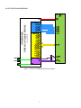
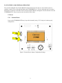
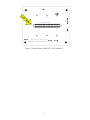
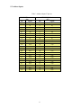
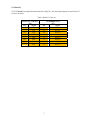
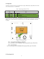
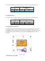
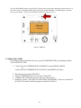
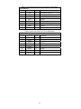
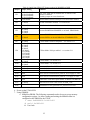
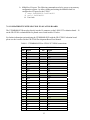
Standard Products
UT8MR8M8-EVB 64Megabit NonVolatile MRAM Evaluation Board
User Manual
July 2012
www.aeroflex.com/memories
1.0 INTRODUCTION
The Aeroflex 64Megabit Non-Volatile magnetoresistive random access memory (MRAM) is a highperformance memory multichip module (MCM) compatible with traditional asynchronous SRAM
operations, organized as four individual 16,777,216 words by 8 bits. The MRAM is equipped with five
chip enables (/En), a single write enable (/W), and a single output enable (/G) pin, allowing for significant
system design flexibility without bus contention. Data is non-volatile for > 15 years at temperature and
data is automatically protected against power loss by a low voltage write inhibit.
The UT8MR8M8-EVB allows the user access to most all the features of the 64Mb MRAM via bench top
evaluation or using the UT699 LEON-3FT evaluation board.
2.0 SCOPE
This document describes the features and necessary steps to set-up and operate the Aeroflex Colorado Springs
64Megabit Non-Volatile MRAM Evaluation Board. Users must be familiar with the UT699 LEON-3FT Processor
and the 64Megabit Non-Volatile MRAM datasheets.
3.0 REFERENCE DOCUMENTS
Aeroflex Colorado Springs, “UT8MR8M8 64Megabit Non-Volatile MRAM” Datasheet,
www.aeroflex.com/memories
Aeroflex Gaisler “GR-CPCI-UT699 LEON3-FT CPCI Development Board” User Manual,
www.aeroflex.com/LEON
Aeroflex Colorado Springs, “UT699 32-bit Fault Tolerant SPARCTM V8/LEON3FT Processor” Datasheet,
www.aeroflex.com/LEON
1
(64-Lead FP MCM)
UT8MR8M8
64M Non-Volatile MRAM
4.0 FUNCTIONAL DIAGRAM
Figure 1. Notional UT8MR8M8-EVB block diagram
2
5.0 FEATURES AND GENERAL OPERATION
The Aeroflex 64Megabit Non-Volatile MRAM Evaluation Board provides the user with a flexible means to
configure, control, access, and read/write data to the UT8MR8M8 device. Power to the board may be provided
through the J9 connector on the GR-UT699 CPCI Development Board or through the 100 mil connector J8 on the
UT8MR8M8-EVB. Only one power source should be used at a time.
5.1 Power
5.1.1
External Power
Power to the UT8MR8M8-EVB may be provided externally using 3.3V if using in a bench top only
configuration.
Figure 2. External Power Jumper Configuration Settings
3
5.1.2
Aeroflex Gaisler Board Power
Power to the UT8MR8M8-EVB is also provided from the J9 connector on the GR-CPCI-UT699 LEON3FT CPCI Development Board. J7, the 120 pin connector, is located on the back side of the EVB.
Use caution when mating the 64Megabit Non-Volatile MRAM Evaluation Board to the LEON-3FT
evaluation board. Ensure that the mating connectors are lined up and that the power is removed from the
GR-cPCI-UT699 eval board prior to plugging in the MRAM evaluation board.
Table 1. LEON-3FT-EVB Power Pins (J9)
Table 2. LEON-3FT-EVB Ground pins (J9)
LEON-3FT connector
Pin
Signal
10
3.3V
20
3.3V
30
3.3V
40
3.3V
51
3.3V
71
3.3V
81
3.3V
91
3.3V
101
3.3V
111
3.3V
LEON-3FT connector
Pin
Signal
1
VSS
3
VSS
5
VSS
7
VSS
11
VSS
21
VSS
31
VSS
41
VSS
50
VSS
60
VSS
61
VSS
70
VSS
80
VSS
90
VSS
100
VSS
110
VSS
114
VSS
116
VSS
118
VSS
120
VSS
4
Figure 3. Aeroflex Gaisler LEON-3FT J7 to J9 connector
5
5.2 Address Inputs
Table 3. Address Inputs J7 pin out
LEON-3FT connector
(J9)
Pin
Signal
45
A0
76
A1
44
A2
77
A3
43
A4
78
A5
42
A6
79
A7
39
A8
82
A9
38
A10
83
A11
37
A12
84
A13
36
A14
85
A15
35
A16
86
A17
34
A18
87
A19
33
A20
88
A21
32
A22
Pin
10
9
8
7
6
28
27
26
25
24
41
40
39
38
37
58
57
56
55
11
59
22
23
6
UT8MR8M8 Device
(J7)
Signal
A0
A1
A2
A3
A4
A5
A6
A7
A8
A9
A10
A11
A12
A13
A14
A15
A16
A17
A18
A19
A20
A21
A22
5.3 Data I/O
The UT8MR8M8 has eight bidirectional data lines, DQ[7:0]. The data inputs/outputs are connected to J7
as shown in table 4.
Table 4. Data I/O J7 pin out
LEON-3FT connector
(J9)
Pin
Signal
95
D24
97
D25
99
D26
103
D27
105
D28
107
D29
109
D30
113
D31
Pin
46
47
50
51
14
15
18
19
7
UT8MR8M8 Device
(J7)
Signal
DATA0
DATA1
DATA2
DATA3
DATA4
DATA5
DATA6
DATA7
5.4 Chip Enable
Asserting /E_All allows the device to be addressed as a single, 64Mb memory using address bits A21 and
A22 to decode and select 1 of 4 MRAM die.
Table 5. Enable Signals LEON-3FT (J5)
LEON-3FT connector
(J9)
Pin
Signal
48
ROMSN0
74
IOSN
UT8MR8M8 Device
(J7)
Pin
21
21
Signal
Can be jumpered to /E_ALL for LEON-3FT to control the
UT8MR8M8
Can be jumpered to /E_ALL
The user can exercise either the IOSN or ROMSN0 pin on the LEON-3FT to exercise the /E_All pin on the
MRAM. There is a three pin header, J5, that allows the user to select IOSN or ROMSN0 to control the
/E_All pin.
Figure 6. /E_All header control
5.4.1 Use as an External Memory with LEON
Set J5 to ROMSN0 on the UT8MR8M8-EVB and uninstall JP6 on the UT699-EVB.
5.4.2 Use as IO Space
Set J5 to IOSN option on the UT8MR8M8-EVB and install JP6 on the UT699-EVB.
5.5 Write Enable (/W)
8
/W controls read and write operation. During a read cycle, /G must be asserted to enable the outputs.
Table 6. Write Enable LEON-3FT J7 to J9 connector
LEON-3FT connector
UT8MR8M8 Device
(J9)
(J7)
Pin
Signal
Pin
Signal
46
WEB
42
/W
5.6 Output Enable (/G)
/W controls read and write operation. During a read cycle, /G must be asserted to enable the outputs.
Table 7. Output Enable LEON-3FT J7 to J9 connector
LEON-3FT connector
UT8MR8M8 Device
(J9)
(J7)
Pin
Signal
Pin
Signal
47
OEB
53
/G
5.7 Deep Sleep Power Down (ZZ)
ZZ controls the sleep mode operation. Enabling sleep mode causes all other inputs to be do not cares. ZZ
places all die into internal low power even while system power is still applied to VDD. Pin 12 on the
UT8MR8M8 are routed to a three pin header J2. The center pin on the three pin J2 header is tied to the ZZ
pin, the other pins are tied to VDD and VSS. Please refer to the UT8MR8M8 datasheet for further
information.
UT8MR8M8
Dee
pP
owe
r Do
wn
Figure 7. ZZ pin
5.8 Multi-Bit Error Flag (MBE)
9
The open drain MBE pin drives low when ECC logic detects two bit errors during the current read cycle. It
allows for wired-or of multiple MBE signals when using multiple MRAMs. The MBE signal is routed to
the one pin J6 header. This pin can be monitored if the user chooses to do so.
MBE
UT8MR8M8
Figure 8. MBE pin
6.0 Quick Start Guide
The following steps describe how the user to get the UT8MR8M8-EVB up and running with the
UT699 LEON-3FT EVB.
1. Connect J5to the UT8MR8M8-EVB to ROMSN0 for using MRAM as PROM
- or Connect J5to the UT8MR8M8-EVB to IOSN for using MRAM as IO Space
2.
3.
4.
5.
Disconnect power to the UT699-EVB
Plug the UT8MR8M8-EVB J7 to J9 on the UT699-EVB
Configure DIP switches S3 and S4 as shown in Table 9 and 10.
Reference Section 3 “SETTING UP AND USING THE BOARD” in the user’s manual for
the GR-UT699 board. Install the jumpers as indicated in Table 11.
10
Table 8. Quick Start LEON-3FT S3 8-bit mode Configuration
DIP Switch S3
Switch
Function
Value Comment
1
PIO0
0
8-bit Mode (Closed)
2
PIO1
0
8-bit Mode (Closed)
3
PIO2
0
PROM EDAC disabled (Closed)
4
PIO3
1
(Open)
5
PIO4
1
(Open)
6
PIO5
1
(Open)
7
PIO6
1
(Open)
8
PIO7
1
(Open)
Table 9. Quick Start LEON-3FT S4 Configuration
DIP Switch S4
Switch
Function
Value Comment
1
PIO8
1
(Open)
(Open)
2
PIO9
1
(Open)
3
PIO10
1
(Open)
4
PIO11
1
(Open)
5
PIO12
1
(Open)
6
PIO13
1
(Open)
7
PIO14
1
(Open)
8
PIO15
1
11
Table 10. Quick Start LEON-3FT Jumper settings for ROMSN0 or IOSN
Jumper Jumper Setting
Comment
JP2
1-2: Do Not Install
3-4: Do Not Install
5-6: Do Not Install
7-8: Do Not Install
Do Not Install
Ethernet MDIO interface interrupt is not connected to GPIO4
JP3
1-3: Install
End-stub termination enabled – see section 2.4.1
JP4
1-3: Install
End-stub termination enabled – see section 2.4.1
JP1
JP5
1-2: Install
3-4: Install
5-6: Install
7-8: Install
Do Not Install
ASIC TEST mode pin not enabled DSU is enabled JTAG
interface is enabled.
Watchdog output can cause board reset
Connects RAMSN0 and RAMSN1 to on board SRAM banks
Connects ROMSN0 to on board MRAM on UT8MR8M8-EVB
JP6
JP11
JP12
JP13
1-2: Install
1-2: Install
3-4: Install
1-2: Install
3-4: Install
5-6: Install
7-8: Install
9-10: Install
11-12: Install
13-14: Install
15-16: Install
17-18: Install
19-20: Install
1-2: Install
3-4: Install
1-2: Install
3-4: Install
Install
1-2: Install
1-2: Install
Connects to Front Panel LED indicators
See section 2.9
See section 2.9
JP14
Install
Can be used as current measure point for Vcore supply to ASIC
JP15
Install
Can be used as current measure point for 3.3V supply to ASIC
JP16
Install
Connected to Front Panel push buttons for RESET and BREAK
JP17
1-2: Install
1-2: Install
Main Processor Clock is also source for SPW_CLK
JP7
JP8
JP9
JP10
JP18
Connects IOSN to on board MRAM on UT8MR8M8-EVB
PCI Host Mode clocks to backplane – see section 2.11
PCI Host Mode- Pull ups enabled – see section 2.11
PCI Host Mode – see section 2.11
PCI Host Mode – see section 2.11
Board RESETN also generated PCI_RSTN for PCI Host
6. Power on the UT699-EVB
7. Using GRMON:
a. MRAM as PROM: The following commands need to be run to set up memory
configuration register 1 to allow reading and writing the MRAM when it is
configured as the PROM for the UT699.
i. wmem 0x80000000 0x1803c811
ii. mcfg1 0x1803c811
iii. User code
12
b. MRAM as I/O space: The following commands need to be run to set up memory
configuration register 1 to allow reading and writing the MRAM when it is
configured as I/O space for the UT699.
i. wmem 0x80000000 0x001BC811
ii. mcfg1 0x001BC811
iii. User code
7.0 COMPATIBILITY WITH GR-UT699 EVALUATION BOARD
The UT8MR8M8-EVB can plug directly into the J9 connector on the LEON-3FT evaluation board. J9
on the GR-UT699 evaluation board is pinned out as listed in table 12 below.
For further information on interfacing the UT8MR8M8-EVB with the GR-UT699 Evaluation board
please see the Aeroflex Gaisler GR-UT699 Development Board User Manual.
Table 11. UT8MR8M8-EVB to UT699-3FT LEON connections
LEON-3FT connector
Pin Signal
1
2
+5V
3
4
-12V
5
6
+12V
7
8
D15
9
D7
10
11
12
D14
13
D6
14
D13
15
D5
16
D12
17
D4
18
D11
19
D3
20
21
22
D10
23
D2
24
D9
25
D1
Pin
13
UT8MR8M8 Device
Signal
VSS
NC
VSS
NC
VSS
NC
VSS
NC
NC
3.3V
VSS
NC
NC
NC
NC
NC
NC
NC
NC
3.3V
VSS
NC
NC
NC
NC
26
27
28
29
30
31
32
33
34
35
36
37
38
39
40
41
42
43
44
45
46
47
48
49
50
51
52
53
54
55
56
57
58
59
60
61
62
63
64
65
66
67
68
69
70
D8
D0
A26
A14
A22
A20
A18
A16
A14
A12
A10
A8
23
59
55
57
37
39
41
25
A6
A4
A2
A0
WEB
OEB
ROMSN0
RAMSN4
27
6
8
10
42
53
RAMSN3
RAMSN2
RAMSN1
RAMSN0
RWEN2
RWEN0
BRDYN
RESETN
CLK
BEXCN
RWEN1
RWEN3
RAMOEN0
RAMOEN1
RAMOEN2
RAMOEN3
14
NC
NC
NC
NC
3.3V
VSS
A22
A20
A18
A16
A14
A12
A10
A8
3.3V
VSS
A6
A4
A2
A0
WEB
OEB
ROMSN0
NC
VSS
3.3V
NC
NC
NC
NC
NC
NC
NC
NC
VSS
VSS
NC
NC
NC
NC
NC
NC
NC
NC
VSS
71
72
73
74
75
76
77
78
79
80
81
82
83
84
85
86
87
88
89
90
91
92
93
94
95
96
97
98
99
100
101
102
103
104
105
106
107
108
109
110
111
112
113
114
115
RAMOEN4
RAMSN1
READ
A1
A3
A5
A7
A9
A11
A13
A15
A17
A19
A21
A23
A25
A27
D16
D24
D17
D25
D18
D26
D19
D27
D20
D28
D21
D29
D22
D30
D23
D31
9
7
28
26
24
40
38
58
56
11
22
46
47
50
51
14
15
18
19
+12V
15
3.3V
NC
NC
IOSN
NC
A1
A3
A5
A7
VSS
3.3V
A9
A11
A13
A15
A17
A19
A21
NC
VSS
3.3V
NC
NC
NC
DATA0
NC
DATA1
NC
DATA2
VSS
3.3V
NC
DATA3
NC
DATA4
NC
DATA5
NC
DATA6
VSS
3.3V
NC
DATA7
VSS
NC
116
117
118
119
120
VSS
NC
VSS
NC
VSS
-12V
+5V
16
8.0 BOARD SCHEMATICS
The schematics are for reference ONLY.
17
5
4
3
2
1
Change Block
1 MQ11
VDD3_3V
D
ADR22_138
4
5
6
E1_138_CS
VDD3_3V
A0
A1
A2
E1
E2
E3
VDD
1
2
3
ADR21_138
GND
U1
16
D
O0
O1
O2
O3
O4
O5
O6
O7
15
14
13
12
11
10
9
7
CEB_1
CEB_2
CEB_3
CEB_4
8
54AC138/FP
VDD3_3V
Silkscreen UT8MR8M8(P)
VDD3_3V
R3
DATA4
DATA5
10k
IOSN
DATA6
DATA7
CEB_2
C
Silkscreen
IOSN
J5
ROMSN0
1
2
3
E1_138_CS
ROMSN0
ADR21_138
ADR22_138
ADR9
ADR8
ADR7
ADR6
ADR5
HEADER 3
R7
10k
Silkscreen
VDD
Silkscreen
VSS
OEB
1
2
3
Silkscreen
TO LEON-3FT UT699 EVAL board
J7
HEADER 3
VDD3_3V
DATA3
DATA2
DATA1
DATA0
CEB_3
ADR10
ADR11
ADR12
ADR13
ADR14
J11
R8
10k
HEADER 3
CEB_4
ADR20
ADR15
ADR16
ADR17
ADR18
10k
CEB_1
ADR4
ADR3
ADR2
ADR1
ADR0
ADR19
VDD3_3V
Silkscreen
UT54ACS138E pin G1
R2
1
2
3
64
63
62
61
60
59
58
57
56
55
54
53
52
51
50
49
48
47
46
45
44
43
42
41
40
39
38
37
36
35
34
33
10K
J2
Silkscreen
VSS
R6
Silkscreen
VDD
VSS
VDD
VDD
VSS
NC1
NC4
NC2
NC5
E0_B
E3_B
A4
A20
A3
A15
A2
A16
A1
A17
A0
A18
A19
NC6
ZZ_NUIL
G_B
NC3
NC7
DQ4
DQ3
DQ5
DQ2
VDD
VSS
VSS
VDD
DQ6
DQ1
DQ7
DQ0
E1_B
E2_B
E_B_ALL_NUIH VSS
A21_NUIL MBE_NUO
A22_NUIL
W_B
A9
A10
A8
A11
A7
A12
A6
A13
A5
A14
VSS
VSS
VSS
VSS
VSS
VDD
VDD
VSS
WEB
1
R5
U2
1
2
3
4
5
6
7
8
9
10
11
12
13
14
15
16
17
18
19
20
21
22
23
24
25
26
27
28
29
30
31
32
10k
Silkscreen
ZZ SLEEPY
Silkscreen
J6 MBE
HEADER 1
IOSN
ADR1
ADR3
ADR5
ADR7
UT8MR8M8_MQ9_10
VDD3_3V
ADR9
ADR11
ADR13
ADR15
ADR17
ADR19
ADR21_138
DATA0
DATA1
DATA2
Silkscreen
3.3V POWER VDD3_3V
B
DATA3
DATA5
1
2
1
2
1
2
DATA4
DATA6
Silkscreen
GND
J8
HEADER 2
J9
HEADER 2
J10
HEADER 2
DATA7
VDD3_3V
61
62
63
64
65
66
67
68
69
70
71
72
73
74
75
76
77
78
79
80
81
82
83
84
85
86
87
88
89
90
91
92
93
94
95
96
97
98
99
100
101
102
103
104
105
106
107
108
109
110
111
112
113
114
115
116
117
118
119
120
DGND
CLK
BEXCN
RWEN1
RWEN3
RAMOEN0
RAMOEN1
RAMOEN2
RAMOEN3
DGND
3.3V
RAMOEN4
ROMSN1
IOSN
READ
A1
A3
A5
A7
DGND
3.3V
A9
A11
A13
A15
A17
A19
A21
A23
DGND
3.3V
A25
A27
D16
D24
D17
D25
D18
D26
DGND
3.3V
D19
D27
D20
D28
D21
D29
D22
D30
DGND
3.3V
D23
D31
DGND
+12V
DGND
-12V
DGND
+5V
DGND
DGND
RESETN
BRDYN
RWEN0
RWEN2
RAMSN0
RAMSN1
RAMSN2
RAMSN3
DGND
3.3V
RAMSN4
ROMSN0
OEN
WRITEN
A0
A2
A4
A6
DGND
3.3V
A8
A10
A12
A14
A16
A18
A20
A22
DGND
3.3V
A24
A26
D0
D8
D1
D9
D2
D10
DGND
3.3V
D3
D11
D4
D12
D5
D13
D6
D14
DGND
3.3V
D7
D15
DGND
+12V
DGND
-12V
DGND
5V
DGND
60
59
58
57
56
55
54
53
52
51
50
49
48
47
46
45
44
43
42
41
40
39
38
37
36
35
34
33
32
31
30
29
28
27
26
25
24
23
22
21
20
19
18
17
16
15
14
13
12
11
10
9
8
7
6
5
4
3
2
1
C
ROMSN0
OEB
WEB
ADR0
ADR2
ADR4
ADR6
ADR8
ADR10
ADR12
ADR14
ADR16
ADR18
ADR20
ADR22_138
VDD3_3V
B
CONN_MEZ120
C1
C2
0.1uF0.01uF
C3
C4
0.1uF0.01uF
C5
C6
0.1uF0.01uF
+
C7
47uF
A
A
Aeroflex Colorado Springs
4350 Centennial Blvd.
Colorado Springs
Colorado 80907
64M MRAM EVALUATION BOARD
Size
C
Tuesday, March 20, 2012
5
4
3
2
Scale
CAGE Code
Rev
DWG NO
4350252-000
65342
Sheet
Larsen
1
2
of
2
ORDERING INFORMATION
UT *****
Device Type:
8MR8M8-EVB = 64Megabit Non-Volatile MRAM Evaluation Board
18
Aeroflex Colorado Springs - Datasheet Definition
Advanced Datasheet - Product In Development
Preliminary Datasheet - Shipping Prototype
Datasheet - Shipping QML & Reduced Hi – Rel
19