1
MI802
Intel® Cedar Trail + NM10
Mini-ITX Motherboard
USER’S MANUAL
Version 1.0A
Acknowledgments
AMI BIOS is a trademark of American Megatrends Inc.
PS/2 is a trademark of International Business Machines
Corporation.
Intel and Luna-Pier are registered trademarks of Intel
Corporation.
Microsoft Windows is a registered trademark of Microsoft
Corporation.
Winbond is a registered trademark of Winbond Electronics
Corporation.
All other product names or trademarks are properties of their
respective owners.
ii
MI802 User’s Manual
Table of Contents
Introduction ...................................................... 1
Checklist............................................................................. 2
MI802 Specifications ......................................................... 3
Board Dimensions .............................................................. 4
Installations ...................................................... 5
Installing the Memory......................................................... 6
Setting the Jumpers............................................................. 7
Connectors on MI802 ....................................................... 12
BIOS Setup.......................................................21
Drivers Installation ......................................41
Intel Chipset Software Installation Utility ......................... 42
VGA Drivers Installation .................................................. 43
Realtek HD Audio Driver Installation .............................. 44
LAN Drivers Installation .................................................. 45
Appendix ...........................................................47
A. I/O Port Address Map .................................................. 47
B. Interrupt Request Lines (IRQ)...................................... 48
C. Watchdog Timer Configuration ................................... 49
D. Digital I/O Sample Code ............................................. 53
MI802 User’s Manual
iii
This page is intentionally left blank.
iv
MI802 User’s Manual
INTRODUCTION
Introduction
MI802 is a Mini ITX board (170mm x 170mm) that comes with the Intel
Atom D2550 processor that runs 1.86GHz and has a 1MB L2 cache. The
board is based on the Intel® CG82NM10 PCH chipset and supports two
SODIMM for a maximum memory support of 4GB.
MI802 features the integrated GMA3650 Intel graphics controller and
supports both CRT and DVD-D video display interface, as well asa 24-bit
dual channel interface with the help of Chrontel CH7511B device.
Onboard functional connections are available for two SATA ports, six
COM ports, eight USB 2.0 ports, audio and a PS/2 keyboard/mouse stack
connector. Additional Expansion comes in one slim PCI slot, two Mini
PCI-e(x1) slots. Power connections is with a +12~24V DC in (ATX
4-pin).
Remarks: Currently, the board comes in two versions:
MI802 – with Cedar Trail-D / Atom D2550 1.86G TDP=10W
DDR3-1066MHz SO-DIMM x 2 (w/o ECC), Max. 4GB, Single channel
MI802N – with Cedar Trail-M / Atom N2600 1.6G TDP=3.5W
DDR3-800MHz SO-DIMM x 1 (w/o ECC), Max. 2GB, Single channel
MI802 User’s Manual
1
INTRODUCTION
Checklist
Your MI802 package should include the items listed below.
• The MI802 Mini-ITX motherboard
• This User’s Manual
• 1 CD containing chipset drivers and flash memory utility
• Serial ATA cable
• I/O shield
2
MI802 User’s Manual
INTRODUCTION
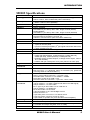
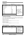
MI802 Specifications
Form Factor
CPU Type
CPU Speed
BIOS
Chipset
Memory
VGA
LVDS
LAN
USB
Serial ATA Ports
Audio
LPC I/O
Digital IO
Keyboard/Mouse
Connector
Expansion Slots
Edge Connector
Onboard Header/
Connector
Watchdog Timer
Power Connector
Others
Board Size
Mini-ITX
®
TM
Intel Atom D2550/N2600 processor (32nm Technology)
22mm x 22mm, Micro-FCBGA559 [TDP=10W/3/5W]
1.86GHz / 1MB L2 cache (MI802)
1.6GHz / 1MB L2 cache (MI802N)
AMI BIOS, support ACPI Function
®
Intel CG82NM10 PCH: 17mm x 17mm, 360-pin BGA (2.1W)
DDR3-1066MHz
SO-DIMM x 2 (w/o ECC), Max. 4GB , Single channel (MI802)
DDR3-800MHz
SO-DIMM x 1 (w/o ECC), Max. 2GB , Single channel (MI802N)
Intel® Integrated Graphics Controller (GMA3650)
Supports DirectX 9 Graphic, OpenGL 3.0
Interface: CRT and DVI-D (thru level shifter ASM1442)
Chrontel CH7511B for 24-bit dual channel LVDS interface
Realtek 8111E-VL GbE x 2
NM10 built-in USB 2.0 host controller, support 8 ports
- 4 ports in the rear panel
rd
- 3 ports for onboard pin header (3 port signal shared with Mini PCIe)
- 2 ports via Mini PCIe slot
NM10 built-in SATA controller, supports 2 ports
NM10 built-in HD audio controller w/ Realtek ALC269QHD Codec
Fintek F81866AD-I:
- COM1 (RS-232/422/485), COM2 (RS-232), COM3 (RS-232),
COM4 (RS-232), COM5 (RS-232), COM6 (RS-232)
- Hardware monitor (2 thermal inputs, 4 voltage monitor inputs, VID0~4
& 2 x Fan Header)
- COM1/2 with pin-9 with power for 2 ports (500 mA for each port)
4 in & 4 out
Yes
Slim PCI slot x 1
Mini PCI-e(x1) x 2, Mounting holes for full-sized (x2) [Reserved
mounting holes for Half-sized also x1]
PS/2 KB+MS stack connector x 1
DB15 + DVI-D stack connector x 1 for CRT + DVI
Dual DB9 stack connector x1 for COM#1 + COM#2
Dual USB + RJ45 x2 for USB + LAN
HD Audio Jack 3x1 connector x 1 (Line-out, Line-in, MIC)
2x4 pin header x 1 for 2 USB ports
1x5 pin header x 1 for USB 4 [Shared with Mini PCIe USB signal]
2x6 pin header x 1 for front audio
DF11 type 10 pin box header x 4 for COM # 3~6
2x5 pin header x 1 for Digital I/O
DF13 box header x 2 for LVDS
4 pin box header x1 for LCD backlight control
SATA connector x 2
4-pin HDD power connector x 2 for SATA device
4-pin ATX power connector for DC-in power
4-pin header for speaker out (from ALC269 internal amplifier)
Yes (256 segments, 0, 1, 2…255 sec/min)
+12~24V DC-in (ATX 4-pins)
1. iSMART function [Auto-scheduler & Power fail resume ]
ST
2. EuP/ErP thru Super I/O [WOL from 1 GbE]
170mm x 170mm
MI802 User’s Manual
3
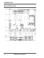
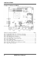
INTRODUCTION
Board Dimensions
4
MI802 User’s Manual
INSTALLATIONS
Installations
This section provides information on how to use the jumpers and
connectors on the MI802 in order to set up a workable system. The topics
covered are:
Installing the Memory .......................................................................... 6
Setting the Jumpers .............................................................................. 7
Connectors on MI802 ........................................................................ 12
MI802 User’s Manual
5
INSTALLATIONS
Installing the Memory
The MI802 board supports two DDR3-1066 memory.
The MI802N board supports one DDR3-800 memory.
Remarks:
D2550 supports SO-DIMM x 2 (w/o ECC), Max. 4GB, Single channel
N2600 supports SO-DIMM x 1 (w/o ECC), Max. 2GB, Single channel
Installing and Removing Memory Modules
To install the DDR3 modules, locate the memory slot on the board and
perform the following steps:
1. Hold the DDR3 module so that the key of the DDR3 module aligned
with that on the memory slot.
2. Gently push the DDR3 module in an upright position until the clips of
the slot close to hold the DDR3 module in place when the DDR3
module touches the bottom of the slot.
3. To remove the DDR3 module, press the clips with both hands.
Lock
DDR3 Module
Lock
6
Lock
Lock
MI802 User’s Manual
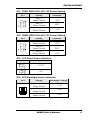
INSTALLATIONS
Setting the Jumpers
Jumpers are used on MI802 to select various settings and features
according to your needs and applications. Contact your supplier if you
have doubts about the best configuration for your needs. The following
lists the connectors on MI802 and their respective functions.
Jumper Locations on MI802 ................................................................ 8
JP1: COM1 RS232 RI/+5V/+12V Power Setting ................................. 9
JP2: COM2 RS232 RI/+5V/+12V Power Setting ................................. 9
JP3: LCD Panel Power Selection ......................................................... 9
JP4: LCD Backlight Power Selection ................................................... 9
JP5: LCD BackLight Control Selection .............................................. 10
JP7: Clear CMOS Setting .................................................................. 10
JP8: LCD BackLight Control Output Level........................................ 10
JP9: LCD Boot ROM Protect (factory use only) ................................ 10
SW1: Panel Type Selection ................................................................ 10
MI802 User’s Manual
7
INSTALLATIONS
Jumper Locations on MI802
Jumper Locations on MI802 ........................................................... Page
JP1: COM1 RS232 RI/+5V/+12V Power Setting................................. 9
JP2: COM2 RS232 RI/+5V/+12V Power Setting................................. 9
JP3: LCD Panel Power Selection ......................................................... 9
JP4: LCD Backlight Power Selection ................................................... 9
JP5: LCD BackLight Control Selection.............................................. 10
JP7: Clear CMOS Setting .................................................................. 10
JP8: LCD BackLight Control Output Level ....................................... 10
JP9: LCD Boot ROM Protect (factory use only) ................................ 10
SW1: Panel Type Selection ................................................................ 10
8
MI802 User’s Manual
INSTALLATIONS
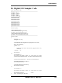
JP1: COM1 RS232 RI/+5V/+12V Power Setting
JP1
Setting
Function
Pin 1-2
Short/Closed
Pin 3-4
Short/Closed
Pin 5-6
Short/Closed
+12V
RI*
+5V
JP2: COM2 RS232 RI/+5V/+12V Power Setting
JP2
Setting
Function
Pin 1-2
Short/Closed
Pin 3-4
Short/Closed
Pin 5-6
Short/Closed
+12V
RI*
+5V
JP3: LCD Panel Power Selection
JP3
LCD Panel Power
+3.3V*
+5V
JP4: LCD Backlight Power Selection
JP4
1
3
5
Setting
2
4
6
Pin 1-2
Short/Closed
Pin 3-4
Short/Closed
Pin 5-6
Short/Closed
Backlight Voltage
+3.3V
+5V
+12V*
MI802 User’s Manual
9
INSTALLATIONS
JP5: LCD BackLight Control Selection
JP5
Setting
Super I/O*
Reserved
JP7: Clear CMOS Setting
JP7
Setting
Normal*
Clear CMOS
JP8: LCD BackLight Control Output Level
JP8
Setting
1
2
+3.3V*
1
2
+5V
JP9: LCD Boot ROM Protect (factory use only)
JP9
Setting
1
2
Write
1
2
Normal*
*Default
SW1: Panel Type Selection
8765
ON
1234
1234
Default: Pin 1,2,3,4 OFF(1111)
10
MI802 User’s Manual
INSTALLATIONS
SW1-4
SW1-3
SW1-2
SW1-1
Panel Type
ON
ON
ON
ON
800*600 18bit 1ch
ON
ON
ON
OFF
1024*768 18bit 1ch
ON
ON
OFF
ON
1024*768 24bit 1ch
ON
ON
OFF
OFF
1280*768 18bit 1ch
ON
OFF
ON
ON
1280*800 18bit 1ch
ON
OFF
ON
OFF
1280*960 18bit 1ch
ON
OFF
OFF
ON
1280*1024 24bit 2ch
ON
OFF
OFF
OFF
1366*768 18bit 1ch
OFF
ON
ON
ON
1366*768 24bit 1ch
OFF
ON
ON
OFF
1440*900 24bit 2ch
OFF
ON
OFF
ON
1440*1050 24bit 2ch
OFF
ON
OFF
OFF
1600*900 24bit 2ch
OFF
OFF
ON
ON
1680*1050 24bit 2ch
OFF
OFF
ON
OFF
1600*1200 24bit 2ch
OFF
OFF
OFF
ON
1920*1080 24bit 2ch
OFF
OFF
OFF
OFF
1920*1200 24bit 2ch
MI802 User’s Manual
11
INSTALLATIONS
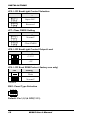
Connectors on MI802
The connectors on MI802 allows you to connect external devices such as
keyboard, floppy disk drives, hard disk drives, printers, etc. The following
table lists the connectors on MI802 and their respective functions.
Connector Locations on MI802 ......................................................... 13
CN6: PS/2 Keyboard and PS/2 Mouse Connectors ............................ 14
CN7: COM1/RS232/422/485, COM2/RS232 Serial Port ................... 14
CN9: VGA and DVI-D Connector ..................................................... 15
CN15: GbE 1st RJ-45 and USB0/1 Ports ........................................... 15
CN19: GbE 2nd RJ-45 and USB2/3 Ports .......................................... 15
CN22: Line-in, Line-out & Microphone Connector ............................ 15
CN1, CN2, CN3, CN4: COM3/4/5/6 RS232 Serial Port .................... 16
CN5: ATX 4P +12V~24V Connector ................................................ 16
CN8, CN11: HDD Power Connector ................................................. 16
CN10, CN12: LVDS Connectors (1st channel, 2nd channel) .............. 16
CN13: LCD Backlight Connector ...................................................... 17
CN14, CN16: SATA Connectors ....................................................... 17
CN17: USB6/7 Ports Header ............................................................. 17
CN18: iSMART JTAG Pin Header (factory use only) ........................ 17
CN20, CN21: Mini PCIE Connector .................................................. 17
CN23: Audio Connector (DF11 Connector)....................................... 18
CN24: Speaker Connector (JST Connector) ...................................... 18
CPU_FAN1: CPU Fan Power Connector ........................................... 18
DIMM1, DIMM2: DDR3 SO-DIMM ................................................ 18
J1: LPC Debug Connector (factory use only) ..................................... 18
J2: Digital I/O .................................................................................... 18
J3: System Function Connector.......................................................... 19
J5: USB4 Port ................................................................................... 19
J6: SPI Flash Connector (factory use only)......................................... 19
PCI1: PCI Slot (supports 2 Master) ................................................... 19
SYS_FAN1: System Fan Power Connector ....................................... 19
12
MI802 User’s Manual
INSTALLATIONS
Connector Locations on MI802
MI802 User’s Manual
13
INSTALLATIONS
CN6: PS/2 Keyboard and PS/2 Mouse Connectors
PS/2 Mouse
PS/2 Keyboard
Signal Name
Keyboard data
N.C.
GND
+5V
Keyboard clock
N.C.
Keyboard
1
2
3
4
5
6
Mouse
7
8
9
10
11
12
Signal Name
Mouse data
N.C.
GND
+5V
Mouse clock
N.C.
CN7: COM1/RS232/422/485, COM2/RS232 Serial Port
Pin #
Signal Name
RS-232
R2-422
RS-485
[
1
2
3
4
5
6
7
8
9*
DCD
RX
TX
DTR
Ground
DSR
RTS
CTS
RI
TXTX+
RX+
RXGround
NC
NC
NC
NC
* Pin 9 supports RI/+5V/+12V function.
14
MI802 User’s Manual
DATADATA+
NC
NC
Ground
NC
NC
NC
NC
INSTALLATIONS
CN9: VGA and DVI-D Connector
Signal Name
Red
Blue
GND
GND
+5V
N.C.
HSYNC
DDC CLOCK
VGA
Pin #
1
3
5
7
9
11
13
15
Pin #
2
4
6
8
10
12
14
Signal Name
Green
N.C.
GND
GND
GND
DDC DATA
VSYNC
[[[[
Signal Name
DATA 2DATA 2+
Shield 2
N.C.
N.C.
DDC CLOCK
DDC DATA
N.C
DATA 1DATA 1+
SHIELD 1
N.C.
N.C.
+5V
GROUND
DVI-D
Pin #
1
2
3
4
5
6
7
8
9
10
11
12
13
14
15
Pin #
16
17
18
19
20
21
22
23
24
C1
C2
C3
C4
C5
C6
Signal Name
HOT PLUG
DATA 0DATA 0+
SHIELD 0
N.C.
N.C.
SHIELD CLK
CLOCKCLOCK+
N.C.
N.C.
N.C.
N.C.
N.C.
N.C.
CN15: GbE 1st RJ-45 and USB0/1 Ports
CN19: GbE 2nd RJ-45 and USB2/3 Ports
CN22: Line-in, Line-out & Microphone Connector
L-IN
L-OUT
MIC
MI802 User’s Manual
15
INSTALLATIONS
CN1, CN2, CN3, CN4: COM3/4/5/6 RS232 Serial Port
2X5_2.0mm_Straight_Male_DF11 (Haoguo DF11-10S-PA66H, Mating
connector: Hirose DF11-10DS-2C or compatible)
1
9
2
10
Signal Name
DCD, Data carrier detect
TXD, Transmit data
GND, ground
RTS, Request to send
RI, Ring indicator
Pin # Pin #
Signal Name
1
2
RXD, Receive data
3
4
DTR, Data terminal ready
5
6
DSR, Data set ready
7
8
CTS, Clear to send
9
10
Not Used
CN5: ATX 4P +12V~24V Connector
[[[[
Signal Name
GND
+12~24V
Pin #
1
3
Pin # Signal Name
2
GND
4
+12~24V
CN8, CN11: HDD Power Connector
1X4_2.5mm_Straight_Male_Wafer (Haoguo W7-03H104142S1WT)
Pin #
Signal Name
1
+5V
2
Ground
4
1
3
Ground
4
+12V
CN10, CN12: LVDS Connectors (1st channel, 2nd channel)
2
20
1
19
DF13-20
16
Signal Name
TX0Ground
TX1+5V/3.3V
TX3TX2Ground
TXC+5V/3.3V
NC
Pin #
2
4
6
8
10
12
14
16
18
20
Pin #
1
3
5
7
9
11
13
15
17
19
Signal Name
TX0+
Ground
TX1+
Ground
TX3+
TX2+
Ground
TXC+
ENABKL
NC
MI802 User’s Manual
INSTALLATIONS
LVDS Connectors: 2X10_1.25mm_Straight_Male_DF13 (Hirose
DF13-20DP-1.25V)
The LVDS (24bit) connectors on board consist of the first channel
(LVDS1) and second channel (LVDS2).
CN13: LCD Backlight Connector
1X4_2.0mm_Straight_M(JST B4B-PH-K-S)
4
Pin #
1
2
3
4
1
Signal Name
+3.3V/5V/12V*
Backlight Enable
Brightness Control
Ground
CN14,CN16: SATA Connectors
7 4 1
Pin #
1
2
3
4
5
6
7
Signal Name
Ground
TX+
TXGround
RXRX+
Ground
CN17: USB6/7 Ports Header
2X4_2.0mm_Straight_Male_DF11 (Haoguo DF11-8S-PA66H, Mating
connector: Hirose DF11-8DS-2C or compatible)
8
2
7
1
Signal Name
+5V
DataData+
Ground
Pin #
1
3
5
7
Pin #
2
4
6
8
Signal Name
Ground
Data+
Data+5V
CN18: iSMART JTAG Pin Header (factory use only)
CN20, CN21: Mini PCIE Connector
Remarks: CN20 USB signal is shared with J5.
MI802 User’s Manual
17
INSTALLATIONS
CN23: Audio Connector (DF11 Connector)
2X6_2.0mm_Straight_Male_DF11 (Haoguo DF11-12S-PA66H, Mating
connector: Hirose DF11-12DS-2C or compatible)
Signal Name Pin # Pin #
Signal Name
LINEOUT_R
2
1
LINEOUT_L
1
2
Ground
4
3
JD LINEOUT
LINEIN R
6
5
LINEIN L
12
11
Ground
8
7
JD_LINEIN
MIC_R
10
9
MIC_L
Ground
12
11
JD MIC1
CN24: Speaker Connector (JST Connector)
1X4_2.5mm_Straight_Male_Wafer (E-CALL 0110-071-040, Mating
connector: JST XHP-4 or compatible)
Pin #
Signal Name
1
Speaker-L+
2
Speaker-L4
1
3
Speaker-R4
Speaker-R+
CPU_FAN1: CPU Fan Power Connector
3
1
Pin #
1
2
3
Signal Name
Ground
+12V
Rotation detection
DIMM1, DIMM2: DDR3 SO-DIMM
J1: LPC Debug Connector (factory use only)
J2: Digital I/O
2X5_2.54mm_Straight_Male_Pin Header (E-CALL 0126-01-203-100)
1
2
3
4
5
6
7
8
9
10
18
Signal Name
GND
OUT3
OUT2
IN3
IN2
Pin #
1
3
5
7
9
Pin #
2
4
6
8
10
Signal Name
+5V
OUT1
OUT0
IN1
IN0
MI802 User’s Manual
INSTALLATIONS
J3: System Function Connector
2X4_2.0mm_Straight_Male_Pin Header (E-CALL 0196-01-200-080)
Signal Name Pin # Pin # Signal Name
2
1
Power BTN
1
2
Power BTN
4
3
Power
LED+
3
4
Power
LED6
5
8
7
HDD LED+
5
6
HDD LEDReset BTN
7
8
Reset BTN
J5: USB4 Port
Remarks: Signal is shared with Mini PCIe(CN20)
1X5_1.25mm_Straight_Male_Wafer (E-CALL 0110-26110050, Mating
connector: Molex 51021-0500 or compatible)
Pin #
Signal Name
1
Ground
2
+5V
5
1
3
Ground
4
Data+
5
DataJ6: SPI Flash Connector (factory use only)
PCI1: PCI Slot (supports 2 Master)
SYS_FAN1: System Fan Power Connector
Pin #
Signal Name
1
Ground
2
+12V
3 1
3
Rotation detection
MI802 User’s Manual
19
INSTALLATIONS
This page is intentionally left blank.
20
MI802 User’s Manual
BIOS SETUP
BIOS Setup
This chapter describes the different settings available in the AMI BIOS
that comes with the board. The topics covered in this chapter are as
follows:
BIOS Introduction ............................................................................. 22
BIOS Setup ....................................................................................... 22
Advanced Settings ............................................................................. 24
Chipset Settings ................................................................................. 33
Boot Settings ..................................................................................... 38
Security Settings ................................................................................ 39
Save & Exit Settings .......................................................................... 40
MI802 User’s Manual
21
BIOS SETUP
BIOS Introduction
The BIOS (Basic Input/Output System) installed in your computer
system’s ROM supports Intel processors. The BIOS provides critical
low-level support for a standard device such as disk drives, serial ports
and parallel ports. It also password protection as well as special support
for detailed fine-tuning of the chipset controlling the entire system.
BIOS Setup
The BIOS provides a Setup utility program for specifying the system
configurations and settings. The BIOS ROM of the system stores the
Setup utility. When you turn on the computer, the BIOS is immediately
activated. Pressing the <Del> key immediately allows you to enter the
Setup utility. If you are a little bit late pressing the <Del> key, POST
(Power On Self Test) will continue with its test routines, thus preventing
you from invoking the Setup. If you still wish to enter Setup, restart the
system by pressing the ”Reset” button or simultaneously pressing the
<Ctrl>, <Alt> and <Delete> keys. You can also restart by turning the
system Off and back On again. The following message will appear on the
screen:
Press
<DEL>
to
Enter
Setup
In general, you press the arrow keys to highlight items, <Enter> to select,
the <PgUp> and <PgDn> keys to change entries, <F1> for help and
<Esc> to quit.
When you enter the Setup utility, the Main Menu screen will appear on
the screen. The Main Menu allows you to select from various setup
functions and exit choices.
22
MI802 User’s Manual
BIOS SETUP
Warning: It is strongly recommended that you avoid making any
changes to the chipset defaults. These defaults have been
carefully chosen by both AMI and your system manufacturer
to provide the absolute maximum performance and
reliability. Changing the defaults could cause the system to
become unstable and crash in some cases.
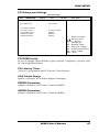
Main
Advanced
Chipset
Boot
Security
Save & Exit
BIOS Information
System Date
Sat 07/21/2012
System Time
13:03:22
→ ← Select
Screen
↑↓ Select Item
Enter: Select
+- Change Opt
F1: General Help
F2: Previous Values
F3: Optimized Default
F4: Save & EXIT
ESC: Exit
System Date
Set the Date. Use Tab to switch between Data elements.
System Time
Set the Time. Use Tab to switch between Data elements.
MI802 User’s Manual
23
BIOS SETUP
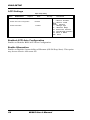
Advanced Settings
This section allows you to configure and improve your system and allows
you to set up some system features according to your preference.
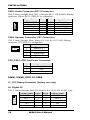
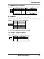
Aptio Setup Utility
Main
Advanced
Chipset
Boot
Security
Save & Exit
Legacy OpROM Support
Launch PXE OpROM
Disabled
Lannch Storage OpROM
Disabled
► PCI Subsystem Settings
► ACPI Settings
► Wake up event setting
► CPU Configuration
→ ← Select
►Auto Power On Schedule
► IDE Configuration
► USB Configuration
► F81866 Super IO Configuration
► FB81866 H/W Monitor
► PPM Configuration
Screen
↑↓ Select Item
Enter: Select
+- Change Opt
F1: General Help
F2: Previous Values
F3: Optimized Default
F4: Save & EXIT
ESC: Exit
Launch PXE OpROM
Enable or Disable Boot Option for Legacy Network Devices.
24
MI802 User’s Manual
BIOS SETUP
PCI Subsystem Settings
Aptio Setup Utility
Main
Advanced
Chipset
PCI Bus Driver Version
Boot
Security
Save & Exit
V 2.05.01
PCI ROM Priority
Legacy ROM
PCI Common Settings
PCI Latency Timer
32 PCI Bus Clocks
VGA Palette Snoop
Disabled
PERR# Generation
Disabled
SERR# Generation
Disabled
→ ← Select
Screen
↑↓ Select Item
Enter: Select
+- Change Opt
F1: General Help
F2: Previous Values
F3: Optimized Default
F4: Save & EXIT
ESC: Exit
PCI ROM Priority
In case of multiple Option ROMs (Legacy and EFI Compatible), specifies what
PCI Option ROM to launch.
PCI Latency Timer
Value to be programmed into PCI Latency Timer Register.
VGA Palette Snoop
Enables or Disables VGA Palette Registers Snooping.
PERR# Generation
Enables or Disables PCI Device to Generate PERR#.
SERR# Generation
Enables or Disables PCI Device to Generate SERR#.
MI802 User’s Manual
25
BIOS SETUP
ACPI Settings
Aptio Setup Utility
Main
Advanced
Chipset
Boot
Security
Save & Exit
ACPI Settings
Enable ACPI Auto Configuration
Enable Hibernation
Disabled
Enabled
→ ← Select
Screen
↑↓ Select Item
Enter: Select
+- Change Opt
F1: General Help
F2: Previous Values
F3: Optimized Default
F4: Save & EXIT
ESC: Exit
Enabled ACPI Auto Configuration
Enables or Disables BIOS ACPI Auto Configuration.
Enable Hibernation
Enables or Disables System ability to Hibernate (OS/S4 Sleep State). This option
may be not effective with some OS.
26
MI802 User’s Manual
BIOS SETUP
Wake Up Event Setting
Aptio Setup Utility
Main
Advanced
Chipset
Boot
Wake on Ring
Disabled
Wake on PCIE PME
Disabled
Security
Save & Exit
→ ← Select
Screen
↑↓ Select Item
Enter: Select
+- Change Opt
F1: General Help
F2: Previous Values
F3: Optimized Default
F4: Save & EXIT
ESC: Exit
Wake on Ring
The options are Disabled and Enabled.
Wake on PCIE PME
The options are Disabled and Enabled.
MI802 User’s Manual
27
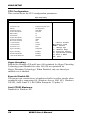
BIOS SETUP
CPU Configuration
This section shows the CPU configuration parameters.
Aptio Setup Utility
Main
Advanced
Chipset
Boot
Security
Save & Exit
CPU Configuration
Processor Type
Intel(R) Atom(TM) CPU
EMT64
Not Supported
Processor Speed
1865 MHz
System Bus Speed
533 MHz
Ratio Status
14
Actual Ratio
14
System Bus Speed
533 MHz
Processor Stepping
30661
Microcode Revision
265
L1 Cache RAM
2x56 k
L2 Cache RAM
2x512 k
Processor Core
Dual
Hyper-Threading
Supported
Hyper-Threading
Enabled
Execute Disable Bit
Enabled
Limit CPUID Maximum
Disabled
→ ← Select
Screen
↑↓ Select Item
Enter: Select
+- Change Opt
F1: General Help
F2: Previous Values
F3: Optimized Default
F4: Save & EXIT
ESC: Exit
Hyper-threading
Enabled for Windows XP and Linux (OS optimized for Hyper-Threading
Technology) and Disabled for other OS (OS not optimized for
Hyper-Threading Technology). When Disabled, only one thread per
enabled core is enabled.
Execute Disable Bit
XD can prevent certain classes of malicious buffer overflow attacks when
combined with a supporting OS (Windows Server 2003 SP1, Windows
XP SP2, SuSE Linux 9.2, Re33dHat Enterprise 3 Update 3.)
Limit CPUID Maximum
Disabled for Windows XP.
28
MI802 User’s Manual
BIOS SETUP
iSmart Controller
Aptio Setup Utility
Main
Advanced
Chipset
Boot
Security
Save & Exit
Auto Power On Schedule
Power-On after Power failure
Disable
Schedule Slot 1
None
Schedule Slot 2
None
→ ← Select
Screen
↑↓ Select Item
Enter: Select
+- Change Opt
F1: General Help
F2: Previous Values
F3: Optimized Default
F4: Save & EXIT
ESC: Exit
EuP/ErP Standby Power Control
Saving the power consumption on power off.
Power-On after Power Failure
This field sets the system power status whether on or off when power returns to
the system from a power failure situation.
Schedule Slot
None / Power On / Power On/Off – Setup the hour/minute for system power on
IDE Configuration
Aptio Setup Utility
Main
Advanced
Chipset
Boot
SATA Port0
Not Present
SATA Port1
Not Present
SATA Controller(s)
Enabled
Configure SATA as
IDE
Security
Save & Exit
→ ← Select
Screen
↑↓ Select Item
Enter: Select
+- Change Opt
F1: General Help
F2: Previous Values
F3: Optimized Default
F4: Save & EXIT
ESC: Exit
SATA Controller(s)
Enable / Disable Serial ATA Controller.
Configure SATA as
(1) IDE Mode.
(2) AHCI Mode.
MI802 User’s Manual
29
BIOS SETUP
USB Configuration
Aptio Setup Utility
Main
Advanced
Chipset
Boot
Security
Save & Exit
USB Configuration
→ ← Select
USB Devices:
None
Legacy USB Support
Enabled
EHCI Hand-off
Enabled
USB hardware delays and time-outs:
USB Transfer time-out
20 sec
Device reset time-out
20 sec
Device power-up delay
Auto
Screen
↑↓ Select Item
Enter: Select
+- Change Opt
F1: General Help
F2: Previous Values
F3: Optimized Default
F4: Save & EXIT
ESC: Exit
Legacy USB Support
Enables Legacy USB support.
AUTO option disables legacy support if no USB devices are connected.
DISABLE option will keep USB devices available only for EFI
applications.
EHCI Hand-off
Enabled/Disabled. This is a workaround for OSes without EHCI hand-off
support. The EHCI ownership change should be claimed by EHCI driver.
USB Transfer Time-out
The time-out value for Control, Bulk, and Interrupt transfers.
Device Reset Time-out
USB mass Storage device start Unit command time-out.
Device Power-up Delay
Maximum time the device will take before it properly reports itself to the
Host Controller. ‘Auto’ uses default value: for a Root port it is 100ms, for
a Hub port the delay is taken from Hub descriptor.
30
MI802 User’s Manual
BIOS SETUP
Super IO Configuration
Aptio Setup Utility
Main
Advanced
Chipset
Boot
Security
Save & Exit
F81866 Super IO Configuration
F81866 Super IO Chip
►Serial
Port 0 Configuration
►Serial
Port 1 Configuration
►Serial
Port 2 Configuration
►Serial
Port 3 Configuration
►Serial
Port 4 Configuration
►Serial
Port 5 Configuration
F81866
Power Failure I
Always off
KB/MS Power on
None
F81866 ERP Support
All Enable
→ ← Select
Screen
↑↓ Select Item
Enter: Select
+- Change Opt
F1: General Help
F2: Previous Values
F3: Optimized Default
F4: Save & EXIT
ESC: Exit
Serial Port Configuration
Set Parameters of Serial Ports. User can Enable/Disable the serial port
and Select an optimal settings for the Super IO Device.
MI802 User’s Manual
31
BIOS SETUP
H/W Monitor
Aptio Setup Utility
Main
Advanced
Chipset
Boot
Security
Save & Exit
PC Health Status
CPU temperature
+52 C
System temperature
+54 C
Fan1 Speed
N/A
Fan2 Speed
N/A
Vcore
+1.208
VCC5V
+5.129V
VCC12V
+11.528 V
+1.5V
+1.520 V
VSB5V
+5.040 V
VCC3V
+3.392 V
VSB3V
+3.376 V
CPU FAN1
Disabled
SYS FAN1
Disabled
→ ← Select
Screen
↑↓ Select Item
Enter: Select
+- Change Opt
F1: General Help
F2: Previous Values
F3: Optimized Default
F4: Save & EXIT
ESC: Exit
Temperatures/Voltages
These fields are the parameters of the hardware monitoring function
feature of the motherboard. The values are read-only values as monitored
by the system and show the PC health status.
CPU Fan1 Control
Options are: Disabled (default), 50 ℃, 60 ℃, 70 ℃, 80 ℃
SYS Fan2 Control
Options are: Disabled (default), 50 ℃, 60 ℃, 70 ℃, 80 ℃
PPM Configuration
Aptio Setup Utility
Main
Advanced
Chipset
Boot
Security
Save & Exit
PPM Configuration
EIST
32
Enabled
MI802 User’s Manual
→ ← Select
Screen
↑↓ Select Item
Enter: Select
+- Change Opt
F1: General Help
F2: Previous Values
F3: Optimized Default
F4: Save & EXIT
ESC: Exit
BIOS SETUP
Chipset Settings
This section allows you to configure and improve your system and allows
you to set up some system features according to your preference.
Aptio Setup Utility
Main
Chipset
Advanced
Boot
Security
Save & Exit
► Host Bridge
→ ← Select
► South Bridge
Screen
↑↓ Select Item
Enter: Select
+- Change Field
F1: General Help
F2: Previous Values
F3: Optimized Default
F4: Save
ESC: Exit
Host Bridge
This item shows the Host Bridge Parameters.
South Bridge
This item shows the South Bridge Parameters.
Host Bridge
This section allows you to configure the Host Bridge Chipset.
Aptio Setup Utility
Main
Advanced
Chipset
Boot
Security
► Memory Frequency and Timing
Save & Exit
→ ←
► Intel IGD Configuration
************Memory Information************
Memory Frequency
1067 MHz(DDR3)
Total Memory
2048 MB
DIMM#0
Not Present
DIMM#1
2048 MB
MI802 User’s Manual
Select Screen
↑↓ Select Item
Enter: Select
+- Change Opt
F1: General Help
F2: Previous Values
F3: Optimized Default
F4: Save & EXIT
ESC: Exit
33
BIOS SETUP
Memory Frequency and Timing
Aptio Setup Utility
Main
Advanced
Chipset
Boot
Security
Save & Exit
Memory Frequency and Timing
MRC Fast Boot
Enabled
Max TOLUD
Dynamic
→ ← Select
Screen
↑↓ Select Item
Enter: Select
+- Change Opt
F1: General Help
F2: Previous Values
F3: Optimized Default
F4: Save & EXIT
ESC: Exit
MRC Fast Boot
The options are Disabled and Enabled.
Max TOLUD
The default setting is Dynamic.
Intel IGD Configuration
Aptio Setup Utility
Main
Advanced
Chipset
Boot
Security
Save & Exit
Intel IGD Configuration
IGFX-Boot Type
VBIOS Default
→ ← Select
Screen
↑↓ Select Item
Enter: Select
+- Change Opt
F1: General Help
F2: Previous Values
F3: Optimized Default
F4: Save & EXIT
ESC: Exit
IGFX-Boot Type
Select the video Device which will be activated during POST.
34
MI802 User’s Manual
BIOS SETUP
South Bridge
This section allows you to configure the South Bridge Chipset.
Aptio Setup Utility
Main
► TPT
Advanced
Chipset
Boot
Security
Save & Exit
Device
► PCI Express
Root Port0
► PCI Express
Root Port1
► PCI Express
Root Port2
► PCI Express
Root Port3
DMI Link ASPM Control
Enabled
PCI-Exp. High Priority Port
Disabled
High Precision Event Timer Configuration
High Precision Timer
Enabled
SLP_SP4 Assertion Width
1-2 Seconds
→ ← Select
Screen
↑↓ Select Item
Enter: Select
+- Change Opt
F1: General Help
F2: Previous Values
F3: Optimized Default
F4: Save & EXIT
ESC: Exit
DMI Clink ASPM Control
The control of Active State Power Management on both NB side and SB
side of the DMI Link.
PCI-Exp. High Priority Port
The options are Disabled, Port1, Port2, Port3, and Port4.
High Precision Event Timer Configuration
Enable/or Disable the High Precision Event Timer.
SLP_S4 Assertion Stretch Enable
Select a minimum assertion width of the SLP_S4# signal.
MI802 User’s Manual
35
BIOS SETUP
TPT Device
Aptio Setup Utility
Main
Advanced
Chipset
Azalia Controller
Boot
Security
→ ← Select
HD Audio
Select USB Mode
By Controllers
UHCI #1 (port 0 and 1)
Enabled
UHCI #2 (port 2 and 3)
Enabled
UHCI #3 (port 4 and 5)
Enabled
UHCI #4 (port 6 and 7)
Enabled
USB 2.0(EHCI) Support
Enabled
Save & Exit
Screen
↑↓ Select Item
Enter: Select
+- Change Opt
F1: General Help
F2: Previous Values
F3: Optimized Default
F4: Save & EXIT
ESC: Exit
PCI Express Root Port0
Aptio Setup Utility
Main
Advanced
Chipset
PCI Express Port 0
Boot
Security
→ ← Select
Enabled
Port 0 IOxAPIC
Disabled
Automatic ASPM
Manual
ASPM L0s
Root Port Only
ASPM L1
Enabled
Save & Exit
Screen
↑↓ Select Item
Enter: Select
+- Change Opt
F1: General Help
F2: Previous Values
F3: Optimized Default
F4: Save & EXIT
ESC: Exit
PCI Express Root Port1
Aptio Setup Utility
Main
Advanced
PCI Express Port 1
Port 0 IOxAPIC
Automatic ASPM
36
Chipset
Boot
Security
Auto
Disabled
Auto
MI802 User’s Manual
Save & Exit
→ ← Select
Screen
↑↓ Select Item
Enter: Select
+- Change Opt
F1: General Help
F2: Previous Values
F3: Optimized Default
F4: Save & EXIT
ESC: Exit
BIOS SETUP
PCI Express Root Port2
Aptio Setup Utility
Main
Advanced
Chipset
PCI Express Port 2
Boot
Security
→ ← Select
Auto
Port 0 IOxAPIC
Disabled
Automatic ASPM
Save & Exit
Screen
↑↓ Select Item
Enter: Select
+- Change Opt
F1: General Help
F2: Previous Values
F3: Optimized Default
F4: Save & EXIT
ESC: Exit
Auto
PCI Express Root Port3
Aptio Setup Utility
Main
Advanced
PCI Express Port 3
Port 0 IOxAPIC
Automatic ASPM
Chipset
Boot
Security
Enabled
Disabled
Auto
MI802 User’s Manual
Save & Exit
→ ← Select
Screen
↑↓ Select Item
Enter: Select
+- Change Opt
F1: General Help
F2: Previous Values
F3: Optimized Default
F4: Save & EXIT
ESC: Exit
37
BIOS SETUP
Boot Settings
Aptio Setup Utility
Main
Advanced
Chipset
Boot
Security
Save & Exit
Boot Configuration
Setup Prompt Timeout
1
Bootup NumLock State
On
Quiet Boot
Disabled
Fast Boot
Disabled
CSM16 Module Version
07.68
GateA20 Active
Upon Request
Option ROM Messages
Force BIOS
Interrupt 19 Canture
Enabled
CSM Support
Enabled
Boot Option Priorities
→ ← Select
Screen
↑↓ Select Item
Enter: Select
+- Change Opt
F1: General Help
F2: Previous Values
F3: Optimized Default
F4: Save & EXIT
ESC: Exit
Setup Prompt Timeout
Number of seconds to wait for setup activation key.
65535(0xFFFF) means indefinite waiting.
Bootup NumLock State
Select the keyboard NumLock state.
Quiet Boot
Enables/Disables Quiet Boot option.
Fast Boot
Enables/Disables boot with initialization of a minimal set of devices required
to launch active boot option. Has no effect for BBS boot options.
GateA20 Active
UPON REQUEST – GA20 can be disabled using BIOS services.
ALWAYS – do not allow disabling GA20; this option is useful when any RT
code is executed above 1MB.
Option ROM Messages
Set display mode for Option ROM. Options: Force BIOS and Keep Current.
Interrupt 19 Capture
Enable: Allows Option ROMs to trap Int 19.
CSM Support
Enables/Disables/Auto CSM Support.
38
MI802 User’s Manual
BIOS SETUP
Security Settings
This section allows you to configure and improve your system and allows
you to set up some system features according to your preference.
Aptio Setup Utility
Main
Advanced
Chipset
Boot
Security
Save & Exit
Password Description
If ONLY the Administrator’s password is set, then
this only limits access to Setup and is only asked
for when entering Setup.
If ONLY the User’s password is set, then this is a
power on password and must be entered to boot or
enter Setup. In Setup the User will have
Administrator rights
Administrator Password
User Password
→ ← Select
Screen
↑↓ Select Item
Enter: Select
+- Change Opt
F1: General Help
F2: Previous Values
F3: Optimized Default
F4: Save & EXIT
ESC: Exit
Administrator Password
Set Setup Administrator Password.
User Password
Set User Password.
MI802 User’s Manual
39
BIOS SETUP
Save & Exit Settings
Aptio Setup Utility
Main
Advanced
Chipset
Boot
Save & Exit
Security
Save Changes and Exit
Discard Changes and Exit
Save Changes and Reset
→ ← Select
Discard Changes and Reset
Save Options
Save Changes
Discard Changes
Restore Defaults
Save as User Defaults
Restore User Defaults
Boot Override
Save Changes and Exit
Exit system setup after saving the changes.
Discard Changes and Exit
Exit system setup without saving any changes.
Save Changes and Reset
Reset the system after saving the changes.
Discard Changes and Reset
Reset system setup without saving any changes.
Save Changes
Save Changes done so far to any of the setup options.
Discard Changes
Discard Changes done so far to any of the setup options.
Restore Defaults
Restore/Load Defaults values for all the setup options.
Save as User Defaults
Save the changes done so far as User Defaults.
Restore User Defaults
Restore the User Defaults to all the setup options.
40
Screen
↑↓ Select Item
Enter: Select
+- Change Opt
F1: General Help
F2: Previous Values
F3: Optimized Default
F4: Save & EXIT
ESC: Exit
MI802 User’s Manual
DRIVERS INSTALLATION
Drivers Installation
This section describes the installation procedures for software and
drivers. The software and drivers are included with the motherboard. If
you find the items missing, please contact the vendor where you made the
purchase. The contents of this section include the following:
Intel Chipset Software Installation Utility ........................................... 42
VGA Drivers Installation ................................................................... 43
Realtek HD Audio Driver Installation ................................................ 44
LAN Drivers Installation .................................................................... 45
IMPORTANT NOTE:
After installing your Windows operating system, you must install first the
Intel Chipset Software Installation Utility before proceeding with the
drivers installation.
MI802 User’s Manual
41
DRIVERS INSTALLATION
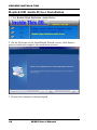
Intel Chipset Software Installation Utility
The Intel Chipset Drivers should be installed first before the software
drivers to enable Plug & Play INF support for Intel chipset components.
Follow the instructions below to complete the installation.
1. Insert the disc that comes with the board. Click Intel and then Intel(R)
Cedarview Chipset Drivers.
2. Click Intel(R) Chipset Software Installation Utility.
3. When the Welcome screen to the Intel® Chipset Device Software
appears, click Next to continue.
4. Click Yes to accept the software license agreement and proceed with
the installation process.
5. On the Readme File Information screen, click Next to continue the
installation.
6. The Setup process is now complete. Click Finish to restart the
computer and for changes to take effect.
42
MI802 User’s Manual
DRIVERS INSTALLATION
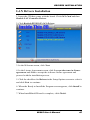
VGA Drivers Installation
1. Click Intel(R) Cedarview Graphics Driver.
2. When the Welcome screen appears, click Next to continue.
4. Click Yes to to agree with the license agreement and continue the
installation.
5. On the Readme File Information screen, click Next to continue the
installation of the Intel® Graphics Media Accelerator Driver.
6. On Setup Progress screen, click Next to continue.
7. Setup complete. Click Finish to restart the computer and for changes
to take effect.
MI802 User’s Manual
43
DRIVERS INSTALLATION
Realtek HD Audio Driver Installation
1. Click Realtek High Definition Audio Driver.
2. On the Welcome to the InstallShield Wizard screen, click Next to
proceed with and complete the installation process.
3. Restart the computer when prompted.
44
MI802 User’s Manual
DRIVERS INSTALLATION
LAN Drivers Installation
1. Insert the CD that comes with the board. Click LAN Card and then
Realtek LAN Controller Drivers.
2. Click Realtek RTL8111E LAN Drivers.
3. In the Welcome screen, click Next.
4. In the License Agreement screen, click I accept the terms in license
agreement and Next to accept the software license agreement and
proceed with the installation process.
5. Click the checkbox for Drivers in the Setup Options screen to select it
and click Next to continue.
6. When the Ready to Install the Program screen appears, click Install to
continue.
7. When InstallShield Wizard is complete, click Finish.
MI802 User’s Manual
45
DRIVERS INSTALLATION
This page is intentionally left blank.
46
MI802 User’s Manual
APPENDIX
Appendix
A. I/O Port Address Map
Each peripheral device in the system is assigned a set of I/O port
addresses that also becomes the identity of the device. The following table
lists the I/O port addresses used.
Address
000h - 01Fh
020h - 03Fh
040h - 05Fh
060h - 06Fh
070h - 07Fh
080h - 09Fh
0A0h - 0BFh
0C0h - 0DFh
0F0h
0F1h
1F0h - 1F7h
2B0h - 2DFh
2E8h - 2EFh
2F8h - 2FFh
360h - 36Fh
3B0h - 3BFh
3C0h - 3CFh
3D0h - 3DFh
3E8h - 3EFh
3F8h - 3FFh
Device Description
DMA Controller #1
Interrupt Controller #1
Timer
Keyboard Controller
Real Time Clock, NMI
DMA Page Register
Interrupt Controller #2
DMA Controller #2
Clear Math Coprocessor Busy Signal
Reset Math Coprocessor
IDE Interface
Graphics adapter Controller
Serial Port #4(COM4)
Serial Port #2(COM2)
Network Ports
Monochrome & Printer adapter
EGA adapter
CGA adapter
Serial Port #3(COM3)
Serial Port #1(COM1)
MI802 User’s Manual
47
APPENDIX
B. Interrupt Request Lines (IRQ)
Peripheral devices use interrupt request lines to notify CPU for the service
required. The following table shows the IRQ used by the devices on
board.
Level
IRQ0
IRQ1
IRQ2
IRQ3
IRQ4
IRQ5
IRQ6
IRQ7
IRQ8
IRQ9
IRQ10
IRQ11
IRQ12
IRQ13
IRQ14
48
Function
System Timer Output
Keyboard
Interrupt Cascade
Serial Port #2
Serial Port #1
Reserved
Reserved
Reserved
Real Time Clock
Reserved
Serial Port #4
Serial Port #3
PS/2 Mouse
80287
Primary IDE
MI802 User’s Manual
APPENDIX
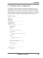
C. Watchdog Timer Configuration
The WDT is used to generate a variety of output signals after a user
programmable count. The WDT is suitable for use in the prevention of
system lock-up, such as when software becomes trapped in a deadlock.
Under these sorts of circumstances, the timer will count to zero and the
selected outputs will be driven. Under normal circumstance, the user will
restart the WDT at regular intervals before the timer counts to zero.
SAMPLE CODE:
//--------------------------------------------------------------------------#include <dos.h>
#include <conio.h>
#include <stdio.h>
#include <stdlib.h>
#include "F81866.H"
//--------------------------------------------------------------------------int main (int argc, char *argv[]);
void EnableWDT(int);
void DisableWDT(void);
//--------------------------------------------------------------------------int main (int argc, char *argv[])
{
unsigned char bBuf;
unsigned char bTime;
char **endptr;
char SIO;
printf("Fintek 81865 watch dog program\n");
SIO = Init_F81866();
if (SIO == 0)
{
printf("Can not detect Fintek 81865, program abort.\n");
return(1);
}//if (SIO == 0)
if (argc != 2)
{
printf(" Parameter incorrect!!\n");
return (1);
}
bTime = strtol (argv[1], endptr, 10);
printf("System will reset after %d seconds\n", bTime);
if (bTime)
{
EnableWDT(bTime); }
else
{
DisableWDT();
}
return 0;
}
//--------------------------------------------------------------------------void EnableWDT(int interval)
{
unsigned char bBuf;
MI802 User’s Manual
49
APPENDIX
bBuf = Get_F81866_Reg(0x2B);
bBuf &= (~0x20);
Set_F81866_Reg(0x2B, bBuf);
//Enable WDTO
Set_F81866_LD(0x07);
Set_F81866_Reg(0x30, 0x01);
//switch to logic device 7
//enable timer
bBuf = Get_F81866_Reg(0xF5);
bBuf &= (~0x0F);
bBuf |= 0x52;
Set_F81866_Reg(0xF5, bBuf);
Set_F81866_Reg(0xF6, interval);
//count mode is second
//set timer
bBuf = Get_F81866_Reg(0xFA);
bBuf |= 0x01;
Set_F81866_Reg(0xFA, bBuf);
//enable WDTO output
bBuf = Get_F81866_Reg(0xF5);
bBuf |= 0x20;
Set_F81866_Reg(0xF5, bBuf);
//start counting
}
//--------------------------------------------------------------------------void DisableWDT(void)
{
unsigned char bBuf;
Set_F81866_LD(0x07);
//switch to logic device 7
bBuf = Get_F81866_Reg(0xFA);
bBuf &= ~0x01;
Set_F81866_Reg(0xFA, bBuf);
//disable WDTO output
bBuf = Get_F81866_Reg(0xF5);
bBuf &= ~0x20;
bBuf |= 0x40;
Set_F81866_Reg(0xF5, bBuf);
//disable WDT
}
//---------------------------------------------------------------------------
50
MI802 User’s Manual
APPENDIX
//--------------------------------------------------------------------------#include "F81866.H"
#include <dos.h>
//--------------------------------------------------------------------------unsigned int F81866_BASE;
void Unlock_F81866 (void);
void Lock_F81866 (void);
//--------------------------------------------------------------------------unsigned int Init_F81866(void)
{
unsigned int result;
unsigned char ucDid;
F81866_BASE = 0x4E;
result = F81866_BASE;
ucDid = Get_F81866_Reg(0x20);
if (ucDid == 0x07)
{
goto Init_Finish;
}
//Fintek 81865
F81866_BASE = 0x2E;
result = F81866_BASE;
ucDid = Get_F81866_Reg(0x20);
if (ucDid == 0x07)
{
goto Init_Finish;
}
//Fintek 81865
F81866_BASE = 0x00;
result = F81866_BASE;
Init_Finish:
return (result);
}
//--------------------------------------------------------------------------void Unlock_F81866 (void)
{
outportb(F81866_INDEX_PORT, F81866_UNLOCK);
outportb(F81866_INDEX_PORT, F81866_UNLOCK);
}
//--------------------------------------------------------------------------void Lock_F81866 (void)
{
outportb(F81866_INDEX_PORT, F81866_LOCK);
}
//--------------------------------------------------------------------------void Set_F81866_LD( unsigned char LD)
{
Unlock_F81866();
outportb(F81866_INDEX_PORT, F81866_REG_LD);
outportb(F81866_DATA_PORT, LD);
Lock_F81866();
}
//--------------------------------------------------------------------------void Set_F81866_Reg( unsigned char REG, unsigned char DATA)
{
Unlock_F81866();
outportb(F81866_INDEX_PORT, REG);
outportb(F81866_DATA_PORT, DATA);
Lock_F81866();
}
//--------------------------------------------------------------------------unsigned char Get_F81866_Reg(unsigned char REG)
{
unsigned char Result;
Unlock_F81866();
outportb(F81866_INDEX_PORT, REG);
Result = inportb(F81866_DATA_PORT);
Lock_F81866();
return Result;
}
//---------------------------------------------------------------------------
MI802 User’s Manual
51
APPENDIX
//--------------------------------------------------------------------------#ifndef __F81866_H
#define __F81866_H
1
//--------------------------------------------------------------------------#define
F81866_INDEX_PORT
(F81866_BASE)
#define
F81866_DATA_PORT
(F81866_BASE+1)
//--------------------------------------------------------------------------#define
F81866_REG_LD
0x07
//--------------------------------------------------------------------------#define F81866_UNLOCK
0x87
#define
F81866_LOCK
0xAA
//--------------------------------------------------------------------------unsigned int Init_F81866(void);
void Set_F81866_LD( unsigned char);
void Set_F81866_Reg( unsigned char, unsigned char);
unsigned char Get_F81866_Reg( unsigned char);
//--------------------------------------------------------------------------#endif //__F81866_H
52
MI802 User’s Manual
APPENDIX
D. Digital I/O Sample Code
Files of the MAIN.CPP
//--------------------------------------------------------------------------#include <dos.h>
#include <conio.h>
#include <stdio.h>
#include <stdlib.h>
#include "F81866.H"
#define BIT0 0x01
#define BIT1 0x02
#define BIT2 0x04
#define BIT3 0x08
#define BIT4 0x10
#define BIT5 0x20
#define BIT6 0x40
#define BIT7 0x80
//--------------------------------------------------------------------------int main (void);
void Dio3Initial(void);
void Dio3SetOutput(unsigned char);
unsigned char Dio3GetInput(void);
void Dio3SetDirection(unsigned char);
unsigned char Dio3GetDirection(void);
//--------------------------------------------------------------------------int main (void)
{
char SIO;
unsigned char DIO;
printf("Fintek 81866 digital I/O test program. Ver 2.0\n");
SIO = Init_F81866();
if (SIO == 0)
{
printf("Can not detect Fintek 81866, program abort.\n");
return(1);
}//if (SIO == 0)
Dio3Initial();
/*
//for GPIO30..37
Dio3SetDirection(0xF0); //GP30..33 = input, GP34..37=output
printf("Current DIO direction = 0x%X\n", Dio3GetDirection());
printf("Current DIO status = 0x%X\n", Dio3GetInput());
printf("Set DIO output to high\n");
Dio3SetOutput(0x0F);
printf("Set DIO output to low\n");
Dio3SetOutput(0x00);
*/
//for GPIO30..37
Dio3SetDirection(0xF0); //GP30..33 = input, GP34..37=output
//
Dio3SetOutput(0x00);
DIO = Dio3GetInput() & 0x0F;
//clear
MI802 User’s Manual
53
APPENDIX
Dio3SetOutput(0x00);
//clear
DIO = Dio3GetInput() & 0x0F;
if (DIO != 0x0A)
{
printf("The Fintek 81866 digital IO abnormal, abort.\n");
return(1);
}//if (DIO != 0x0A)
Dio3SetOutput(0xA0);
Dio3SetOutput(0xF0);
Dio3SetOutput(0xA0);
//clr# is high
//clk and clr# is high
//clr# is high
DIO = Dio3GetInput() & 0x0F;
if (DIO != 0x05)
{
printf("The Fintek 81866 digital IO abnormal, abort.\n");
return(1);
}
printf("!!! Pass !!!\n");
return 0;
}
//--------------------------------------------------------------------------void Dio3Initial(void)
{
unsigned char ucBuf;
// Switch GPIO multi-function pin for gpio 30~37
// Multi Pin Select UART2/GPIOs
// bit[6:5] 0:UART2 / 1:GPIOs
ucBuf = Get_F81866_Reg(0x28);
ucBuf |= BIT5;
Set_F81866_Reg(0x28, ucBuf);
Set_F81866_LD(0x06);
//switch to logic device 6
//enable the GP3 group
ucBuf = Get_F81866_Reg(0x30);
ucBuf |= 0x01;
Set_F81866_Reg(0x30, ucBuf);
Set_F81866_Reg(0x88, 0x00);
//Set_F81866_Reg(0xA3, 0xFF);
}
//--------------------------------------------------------------------------void Dio3SetOutput(unsigned char NewData)
{
Set_F81866_LD(0x06);
Set_F81866_Reg(0x89, NewData);
}
//--------------------------------------------------------------------------unsigned char Dio3GetInput(void)
{
unsigned char result;
Set_F81866_LD(0x06);
result = Get_F81866_Reg(0x8A);
return (result);
}
54
MI802 User’s Manual
//define as input mode
//push pull mode
//switch to logic device 6
//switch to logic device 6
APPENDIX
//--------------------------------------------------------------------------void Dio3SetDirection(unsigned char NewData)
{
//NewData : 1 for input, 0 for output
Set_F81866_LD(0x06);
Set_F81866_Reg(0x88, NewData);
}
//--------------------------------------------------------------------------unsigned char Dio3GetDirection(void)
{
unsigned char result;
Set_F81866_LD(0x06);
result = Get_F81866_Reg(0x88);
return (result);
//switch to logic device 6
//switch to logic device 6
}
//---------------------------------------------------------------------------
MI802 User’s Manual
55
APPENDIX
Files of the F81866.CPP
//--------------------------------------------------------------------------#include "F81866.H"
#include <dos.h>
//--------------------------------------------------------------------------unsigned int F81866_BASE;
void Unlock_F81866 (void);
void Lock_F81866 (void);
//--------------------------------------------------------------------------unsigned int Init_F81866(void)
{
unsigned int result;
unsigned char ucDid;
F81866_BASE = 0x4E;
result = F81866_BASE;
ucDid = Get_F81866_Reg(0x20);
if (ucDid == 0x10)
{
goto Init_Finish; }
//Fintek 81801
F81866_BASE = 0x2E;
result = F81866_BASE;
ucDid = Get_F81866_Reg(0x20);
if (ucDid == 0x07)
{
goto Init_Finish; }
//Fintek 81801
F81866_BASE = 0x00;
result = F81866_BASE;
Init_Finish:
return (result);
}
//--------------------------------------------------------------------------void Unlock_F81866 (void)
{
outportb(F81866_INDEX_PORT, F81866_UNLOCK);
outportb(F81866_INDEX_PORT, F81866_UNLOCK);
}
//--------------------------------------------------------------------------void Lock_F81866 (void)
{
outportb(F81866_INDEX_PORT, F81866_LOCK);
}
//--------------------------------------------------------------------------void Set_F81866_LD( unsigned char LD)
{
Unlock_F81866();
outportb(F81866_INDEX_PORT, F81866_REG_LD);
outportb(F81866_DATA_PORT, LD);
Lock_F81866();
}
//--------------------------------------------------------------------------void Set_F81866_Reg( unsigned char REG, unsigned char DATA)
{
Unlock_F81866();
outportb(F81866_INDEX_PORT, REG);
outportb(F81866_DATA_PORT, DATA);
Lock_F81866();
56
MI802 User’s Manual
APPENDIX
}
//--------------------------------------------------------------------------unsigned char Get_F81866_Reg(unsigned char REG)
{
unsigned char Result;
Unlock_F81866();
outportb(F81866_INDEX_PORT, REG);
Result = inportb(F81866_DATA_PORT);
Lock_F81866();
return Result;
}
//---------------------------------------------------------------------------
MI802 User’s Manual
57
APPENDIX
Files of the F81866.H
//--------------------------------------------------------------------------#ifndef __F81866_H
#define __F81866_H
1
//--------------------------------------------------------------------------#define
F81866_INDEX_PORT
(F81866_BASE)
#define
F81866_DATA_PORT
(F81866_BASE+1)
//--------------------------------------------------------------------------#define
F81866_REG_LD
0x07
//--------------------------------------------------------------------------#define F81866_UNLOCK
0x87
#define
F81866_LOCK
0xAA
//--------------------------------------------------------------------------unsigned int Init_F81866(void);
void Set_F81866_LD( unsigned char);
void Set_F81866_Reg( unsigned char, unsigned char);
unsigned char Get_F81866_Reg( unsigned char);
//--------------------------------------------------------------------------#endif
//__F81866_H
58
MI802 User’s Manual