1
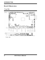
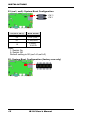
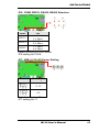
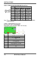
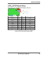
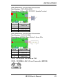
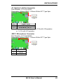
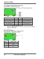
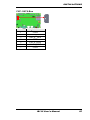
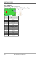
IB112 Freescale I.MX536 ARM Cortex™-A8 Embedded BOARD USER’S MANUAL Version 1.0 Acknowledgments Freescale is a registered trademark of Freescale Semiconductor Inc. All other product names or trademarks are properties of their respective owners. ii IB112 User’s Manual Table of Contents Introduction ....................................................... 5 Product Description............................................................. 5 Checklist .............................................................................. 7 Board Dimensions ............................................................... 8 Installations ..................................................... 10 Setting the Jumpers ........................................................... 11 Connectors on IB112......................................................... 16 IB112 User’s Manual iii This page is intentionally left blank. iv IB112 User’s Manual INTRODUCTION Introduction Product Description The IB112 Embedded board is based on the Freescale I.MX536 Microprocessor. I.MX536 is a high-performance ARM Cortex-A8 microprocessor with speeds up to 800 MHz. The device offers 3D graphics acceleration while also supporting numerous peripherals, including DDR3 and USB OTG that are well suited for industrial applications. The following subsystems are part of the device: • Microprocessor unit (MPU) subsystem based on the ARM Cortex-A8 Microprocessor • OpenGL ES 2.0 3D accelerator • OpenVG 1.1 graphics accelerator • Multi-format HD1080 video decoder • Multi-format HD720 video encoder IB112 User’s Manual 5 INTRODUCTION IB112 FEATURES: 6 Freescale I.MX536 800 MHz ARM Cortex-A8 Microprocessor 1G Byte DDR3 RAM 1 x 18 bit LVDS Connector 1 x 18 bit TTL LCD Connector 2 x COM Port Connector 1 x Mini-PCIe(x1) Slot (w/ USB support Only) 2 x 10/100 Based-T Ethernet (RJ-45) Connector 12V~ 30V DC-IN Power Connector 1 x SD Card Slot, 1x Micro SD 1 x emmc FLASH (Option) 1 x USB OTG 2 x USB Host(1 x USB A-Type, 1 x pin header) 1 x HDMI Port (Option) 1 x VGA Port (Option) 1 x SATA Port (Option) 8 Bits GPIO (Option) Resistive Touch Connector 2 x CANBUS Connector 1 x Microphone / 1 x Speaker IB112 User’s Manual INTRODUCTION Checklist Your IB112 package should include the items listed below. The IB112 Embedded board This User’s Manual IB112 User’s Manual 7 INTRODUCTION [ Board Dimensions Top Side Units: mm 8 IB112 User’s Manual INSTALLATIONS Installations This section provides information on how to use the jumpers and connectors on the IB112 in order to set up a workable system. The topics covered are: Setting the Jumpers .............................................................................. 11 Connectors on IB112 ........................................................................... 16 IB112 User’s Manual 9 INSTALLATIONS Setting the Jumpers Jumpers are used on IB112 to select various settings and features according to your needs and applications. Contact your supplier if you have doubts about the best configuration for your needs. The following lists the connectors on IB112 and their respective functions. Jumper Locations on IB112 ................................................................. 11 S1 (sw1, sw2): System Boot Configuration ......................................... 12 S2: System Boot Configuration (factory use only) ............................... 12 JP9: COM2 RS232, RS422, RS485 Selection ..................................... 14 JP7: USB +3.3V/+5V Power Setting ................................................... 14 J14: LVDS +3.3V/+5V Power Setting ................................................. 15 JP10: LED Brightness +5V/+9.6V/+12V Power Setting ..................... 15 10 IB112 User’s Manual INSTALLATIONS Jumper Locations on IB112 Top Side IB112 User’s Manual 11 INSTALLATIONS S1 (sw1, sw2): System Boot Configuration SW 2 SW 1 S1 (sw1, sw2) Boot From 00 CN6 (SD1) 01 CN8(SD2) EMMC NAND 10 Note: 1: Switch On 0: Switch Off Default setting is 00 (sw1=0,sw2=0) S2: System Boot Configuration (factory use only) 12 IB112 User’s Manual INSTALLATIONS JP9: COM2 RS232, RS422, RS485 Selection 2 6 1 5 Mode JP9 2-4 Short RS232 3-5 Short 3-5 Short RS422 4-6 Short 1-3 Short RS485 4-6 Short Default setting is RS232 mode. JP9 setting for CN18. JP7: USB +3.3V/+5V Power Setting 3 JP7 1 Setting +3.3V +5V Default setting is +5V. JP7 setting for J1. IB112 User’s Manual 13 INSTALLATIONS J14: LVDS +3.3V/+5V Power Setting 1 3 J14 Setting +3.3V +5V Default setting is +3.3V. J14 setting for LVDS1. JP10: LED Brightness +5V/+9.6V/+12V Power Setting 2 6 1 JP10 Setting Pin 3-5 Short/Closed Pin 3-4 Short/Closed Pin 1-3 Short/Closed 5 Function +5V +9.6V +12V Default setting is +5V. JP10 setting for LVDS1. 14 IB112 User’s Manual INSTALLATIONS Connectors on IB112 Connector Locations on IB112 ............................................................ 17 CN6: SD Card Connector .................................................................... 18 CN8: Micro SD Card Connector ........................................................ 18 COM1 PORT: COM1 RS232 Connector ............................................ 18 CN18:COM2 RS232/RS422/RS485 Serial Port .................................. 19 COM3 PORT: COM3 RS232 Connector ............................................ 19 LVDS1: LVDS Display Connector...................................................... 20 CN1: LCD 18 Bit Parallel Signal Connector ....................................... 21 CN2: Resistive Touch Panel Connector............................................... 22 CN3: Resistive Touch Panel Connector............................................... 22 CN15: 10/100Mb LAN1 (From Freescale i.MX536) ......................... 22 CN19: 10/100Mb LAN2 (USB to Ethernet) ....................................... 23 CN4: LED Backlight Control Connector ............................................. 23 J3: Speaker Right Out Connector ........................................................ 23 J5: Speaker Left Out Connector .......................................................... 24 JMIC1: Microphone Connector ........................................................... 24 J10: Digital I/O 4 In/4 Out Connector ................................................. 25 JP2: SATA Power ................................................................................ 25 CN7: SATA Bus .................................................................................. 26 JP1: VGA Port ..................................................................................... 26 J11: External Key Port ......................................................................... 27 SW2: Push Button for Hardware Reset................................................ 27 JP11: Pin Header for Hardware Reset ................................................. 27 BAT: 3.0V Lithium Battery Connector. .............................................. 28 CN14: 12V~30V Power Connector ..................................................... 29 J16: 12V~30V Power Connector ......................................................... 29 JUSB1: USB2.0 Type A Connector .................................................... 30 CN16: Mini USB OTG Connector ...................................................... 30 J1: USB2.0 Connector ......................................................................... 31 J4: Line Out Connector ........................................................................ 31 J12: HDMI connector .......................................................................... 32 JMINI1: Mini PCIE Connector ........................................................... 33 JP8: CANBUS Connector.................................................................... 34 IB112 User’s Manual 15 INSTALLATIONS Connector Locations on IB112 16 IB112 User’s Manual INSTALLATIONS CN6: SD Card Connector CN8: Micro SD Card Connector COM1 PORT: COM1 RS232 Connector (Debug Port, factory use only) Part Number: 0195-01-200-040 Description: Pin Header 2.0*2.0mm S/T Single Row 4pin 1 4 Pin # 1 2 3 4 Signal Name COM1 RX, Receive data COM1 TX, Transmit data GND, ground NC IB112 User’s Manual 17 INSTALLATIONS CN18: COM2 RS232/RS422/RS485 Serial Port Pin # Signal Name RS-232 RS-422 RS-485 1 DCD TXDATA2 RX TX+ DATA+ 3 TX RX+ NC 4 DTR RXNC 5 Ground Ground Ground 6 DSR NC NC 7 RTS NC NC 8 CTS NC NC 9 NC NC NC Note: Please refer to JP9 setting for RS232, RS422 and RS485 mode selection. [ COM3: COM3 RS232 Connector Part Number: DF11-10S-PA66H Description: 2mm DIP Mini 180D 10P 2R Male 1 Pin # 1 2 3 4 5 6 7 8 9 10 18 2 Signal Name RX, Receive data TX, Transmit data NC NC GND, ground NC RTS, Request To Send CTS, Clear To Send NC NC 9 10 IB112 User’s Manual INSTALLATIONS LVDS1: LVDS Display Connector Part Number: DF13-20DP-1.25V(95) Description: P1.25 SMD 20PIN Male 180D 2R 20 2 19 1 Signal Name Pin # Pin # Signal Name TX0+ 1 2 TX0Ground 3 4 Ground TX1+ 5 6 TX1Ground 7 8 +5V/3.3V TX3+ 9 10 TX3TX2+ 11 12 TX2Ground 13 14 Ground TXC+ 15 16 TXCBacklight ADJ 17 18 +5V/3.3V +5V/+9.6V/+12V 19 20 +5V/+9.6V/+12V Note: Please refer to J14 for pin8 and pin18 refer to JP10 for pin19 and pin20 IB112 User’s Manual 19 INSTALLATIONS CN1: LCD 18 Bit Parallel Signal Connector Part Number: CSF-2881-401R Description: 0.50mm ZIF FFC/FPC Downside Connector 1 Signal Name +5V +5V Backlight ADJ GND GND +3.3V +3.3V Mode DE VSYNC HSYNC GND B5(MSB) B4 B3 GND B2 B1 B0 GND 20 Pin # 1 2 3 4 5 6 7 8 9 10 11 12 13 14 15 16 17 18 19 20 Pin # 21 22 23 24 25 26 27 28 29 30 31 32 33 34 35 36 37 38 39 40 40 Signal Name G5(MSB) G4 G3 GND G2 G1 G0 GND R5(MSB) R4 R3 GND R2 R1 R0 GND DCLK GND L/R U/D IB112 User’s Manual INSTALLATIONS CN2: Resistive Touch Panel Connector Part Number: CSF-0782-041R Description: 1.00mm ZIF FPC/FFC Upside Contact 1 Pin # 1 2 3 4 Signal Name Touch YP Touch XP Touch YM Touch XM CN3: Resistive Touch Panel Connector Part Number: 0110-161-040 Description: JST-PH Type Wafer 2.0mm 4Pin 4 1 Pin # Signal Name 1 Touch YP 2 Touch XP 3 Touch YM 4 Touch XM Note: CN3 signals are same as CN2. CN15: 10/100Mb LAN1 (From Freescale i.MX536) IB112 User’s Manual 21 INSTALLATIONS CN19: 10/100Mb LAN2 (USB to Ethernet) CN4: LED Backlight Control Connector Part Number: 0110-2610040 Description: MOLEX 53047 1.25mm Wafer S/T Type 4pin 1 4 Pin # Signal Name 1 +5V/+9.6V/+12V 2 Backlight ADJ 3 Backlight Enable 4 GND Please refer to JP10 setting for +5V, +9.6V and +12V selection. J3: Speaker Right Out Connector Part Number: 0110-2610020 Description: Molex 53047 1.25mm Wafer S/T Type 2pin 1 2 Pin # Signal Name 1 SPEAKER_RIGHT2 SPEAKER_RIGHT+ Note: The maximun output power is 2 W with 4 Ω speaker or 1.4 W with 8 Ω speaker 22 IB112 User’s Manual INSTALLATIONS J5: Speaker Left Out Connector Part Number: 0110-2610020 Description: Molex 53047 1.25mm Wafer S/T Type 2pin 1 2 Pin # Signal Name 1 SPEAKER_LEFT2 SPEAKER_LEFT+ Note: The maximun output power is 2 W with 4 Ω speaker or 1.4 W with 8 Ω speaker JMIC1: Microphone Connector Part Number: 0110-2610020 Description: Molex 53047 1.25mm Wafer S/T Type 2pin 1 2 Pin # Signal Name 1 GND 2 MIC_IN IB112 User’s Manual 23 INSTALLATIONS J10: Digital I/O 4 In/4 Out Connector Part Number: 0196-01-200-100 Description: Pin Header 2.0*2.0mm S/T Dual Rows 2*5pin 1 2 9 10 Signal Name Pin # Pin # Signal Name GND 1 2 +3.3V OUT3 (U46.P17) 3 4 OUT1 (U46.P15) OUT2 (U46.P16) 5 6 OUT0 (U46.P14) IN3 (U46.P13) 7 8 IN1 (U46.P11) IN2 (U46.P12) 9 10 IN0 (U46.P10) Note: All In/Out signals level are 3.3V . U46 is TCA6416PAW IC. The IC connects with i.MX535 CPU via I2C2 port. JP2: SATA Power Part Number: WAFER25-104S-2442-ST Description: 2.5 wafer 4pin 180D 1 Pin # 1 2 3 4 24 4 Signal Name +5V GND GND NC IB112 User’s Manual INSTALLATIONS CN7: SATA Bus Pin # 1 2 3 4 5 6 7 Signal Name GND SATA_TXP SATA_TXN GND SATA_RXN SATA_RXP GND IB112 User’s Manual 25 INSTALLATIONS JP1: VGA Port Part Number: 0196-01-2811615 Description: Pin Header 2.0mm S/T Dual Row 2*8pin Pin # 1 2 3 4 5 6 7 8 9 10 11 12 13 14 15 26 16 15 2 1 Signal Name VGA_R +5V VGA_G GND VGA_B NC NC VGA_I2C_SDA NC VGA_HSYNC GND VGA_VSYNC NC VGA_I2C_SCL GND IB112 User’s Manual INSTALLATIONS J11: External Key Port Part Number: 0110-3221100 Description: Molex 53398 1.25mm Wafer R/A 10pin 10 1 Pin # Signal Name 1 GND 2 USER_KEY1 3 USER_KEY2 4 NC 5 RESET# 6 NC 7 NC 8 NC 9 +3.3V 10 +5V Note: USER_KEY1 is used as RETURN key for Android OS. USER_KEY2 is used as HOME key for Android OS. SW2: Push Button for Hardware Reset IB112 User’s Manual 27 INSTALLATIONS JP11: Pin Header for Hardware Reset Part Number: 0195-01-200-040 Description: PIN HEADER 2.0*2.0mm S/T SINGLE ROW 4PIN 1 Pin # 1 2 3 4 4 Signal Name SW_RST GND GND NC BAT: 3.0V Lithium Battery Connector Part Number: 0110-2610020 Description: Molex 53047 1.25mm Wafer S/T Type 2pin 1 2 Pin # 1 2 Signal Name +VCC GND CN14: 12V~30V Power Connector This connector supplies the system board operating voltage. Pin 1 Pin # 1 2 28 Pin 2 Signal Name +12V ~ +30V GND IB112 User’s Manual INSTALLATIONS J16: 12V~30V Power Connector 2 1 Pin # Signal Name 1 +12V ~ +30V 2 GND Note: J16 signals are same as CN14. IB112 User’s Manual 29 INSTALLATIONS JUSB1: USB2.0 Type A Connector Pin # 1 2 3 4 Signal Name +5V DD+ GND CN16: Mini USB OTG Connector Pin # Signal Name 1 +5V 2 D3 D+ 4 ID 5 GND Note: CN16 used as USB device while ID is floating. (CN16 support USB device only.) 30 IB112 User’s Manual INSTALLATIONS J1: USB2.0 Connector Part Number: B4B-PH-K-S(LF)(SN) Description: Mini Base;DIP S 2mm 4P 1 Pin # 1 2 3 4 4 Signal Name +5V / +3.3V DD+ GND Default setting is +5V. Please refer to JP7 setting for +5V and +3.3V selection. J4: Line Out Connector Part Number: 0110-2610030 Description: Molex 53047 1.25mm Wafer S/T Type 3pin 1 Pin # 1 2 3 3 Signal Name LINE_OUTL GND LINE_OUTR [ IB112 User’s Manual 31 INSTALLATIONS J12: HDMI connector Pin # 1 2 3 4 5 6 7 8 9 10 11 12 13 14 15 16 17 18 19 32 Signal Name TX2+ GND TX2TX1+ GND TX1TX0+ GND TX0TXC+ GND TXCNC NC NC NC GND +5V NC IB112 User’s Manual INSTALLATIONS JMINI1: Mini PCIE Connector Signal Name NC NC NC NC GND NC NC GND NC NC GND NC NC GND GND NC NC GND GND +3.3V +3.3V GND NC NC NC NC Pin # 1 3 5 7 9 11 13 15 17 19 21 23 25 27 29 31 33 35 37 39 41 43 45 47 49 51 Pin # 2 4 6 8 10 12 14 16 18 20 22 24 26 28 30 32 34 36 38 40 42 44 46 48 50 52 Signal Name +3.3V GND NC NC NC NC NC NC GND +3.3V RESET# +3.3V GND NC I2C2_SCL I2C2_SDA GND USB2.0 DUSB2.0 D+ GND NC NC NC NC GND +3.3V IB112 User’s Manual 33 INSTALLATIONS JP8: CANBUS Connector Part Number: 0126-01-203-080 Description: 2.54*2.54mm S/T Dual Rows 2*4pin Signal Name GND_ISO CAN1_H CAN1_L GND 34 Pin # 1 3 5 7 8 7 2 1 Pin # 2 4 6 8 Signal Name GND_ISO CAN2_H CAN2_L GND IB112 User’s Manual APPENDIX IB112 User’s Manual 35