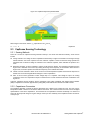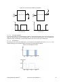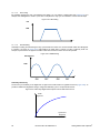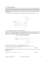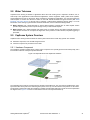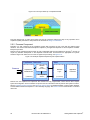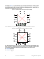
1
Getting Started with CapSense® Document No. 001-64846 Rev.*I Cypress Semiconductor 198 Champion Court San Jose, CA 95134-1709 Phone (USA): 800.858.1810 Phone (Intnl): 408.943.2600 http://www.cypress.com Copyrights Copyrights © Cypress Semiconductor Corporation, 2010-2013. The information contained herein is subject to change without notice. Cypress Semiconductor Corporation assumes no responsibility for the use of any circuitry other than circuitry embodied in a Cypress product. Nor does it convey or imply any license under patent or other rights. Cypress products are not warranted nor intended to be used for medical, life support, life saving, critical control or safety applications, unless pursuant to an express written agreement with Cypress. Furthermore, Cypress does not authorize its products for use as critical components in life-support systems where a malfunction or failure may reasonably be expected to result in significant injury to the user. The inclusion of Cypress products in life-support systems application implies that the manufacturer assumes all risk of such use and in doing so indemnifies Cypress against all charges. Trademarks PSoC Designer™ and SmartSense™ are trademarks and PSoC®, CapSense®, and TrueTouch® are registered trademarks of Cypress Semiconductor Corp. All other trademarks or registered trademarks referenced herein are property of the respective corporations. Source Code Any Source Code (software and/or firmware) is owned by Cypress Semiconductor Corporation (Cypress) and is protected by and subject to worldwide patent protection (United States and foreign), United States copyright laws and international treaty provisions. Cypress hereby grants to licensee a personal, non-exclusive, non-transferable license to copy, use, modify, create derivative works of, and compile the Cypress Source Code and derivative works for the sole purpose of creating custom software and or firmware in support of licensee product to be used only in conjunction with a Cypress integrated circuit as specified in the applicable agreement. Any reproduction, modification, translation, compilation, or representation of this Source Code except as specified above is prohibited without the express written permission of Cypress. Disclaimer CYPRESS MAKES NO WARRANTY OF ANY KIND, EXPRESS OR IMPLIED, WITH REGARD TO THIS MATERIAL, INCLUDING, BUT NOT LIMITED TO, THE IMPLIED WARRANTIES OF MERCHANTABILITY AND FITNESS FOR A PARTICULAR PURPOSE. Cypress reserves the right to make changes without further notice to the materials described herein. Cypress does not assume any liability arising out of the application or use of any product or circuit described herein. Cypress does not authorize its products for use as critical components in life-support systems where a malfunction or failure may reasonably be expected to result in significant injury to the user. The inclusion of Cypress product in a life-support systems application implies that the manufacturer assumes all risk of such use and in doing so indemnifies Cypress against all charges. Use may be limited by and subject to the applicable Cypress software license agreement. 2 Document No. 001-64846 Rev. *I Getting Started with CapSense ® Contents 1. Introduction.................................................................................................................................................................... 6 1.1 1.2 1.3 1.4 2. How to Use This Guide .......................................................................................................................................... 6 Cypress‘s CapSense Documentation Ecosystem .................................................................................................. 6 Cypress CapSense Products................................................................................................................................. 8 1.3.1 Cypress CapSense Differentiation ............................................................................................................ 8 Document Conventions ......................................................................................................................................... 9 CapSense Technology ................................................................................................................................................ 10 2.1 2.2 2.3 2.4 2.5 2.6 2.7 Capacitive Sensing Methods ............................................................................................................................... 10 2.1.1 Self-Capacitance .................................................................................................................................... 10 2.1.2 Mutual-Capacitance ................................................................................................................................ 11 Self-Capacitance Equivalent Model ..................................................................................................................... 11 CapSense Sensing Technology .......................................................................................................................... 12 2.3.1 Sensing Methods .................................................................................................................................... 12 2.3.2 Capacitance Conversion......................................................................................................................... 12 2.3.3 CapSense with Sigma Delta Modulator (CSD) ....................................................................................... 13 2.3.4 CapSense Successive Approximation Electromagnetic Compatible (CSA_EMC) .................................. 14 CapSense Tuning ................................................................................................................................................ 15 2.4.1 Definitions ............................................................................................................................................... 15 2.4.2 Signal-to-Noise Ratio (SNR) ................................................................................................................... 16 2.4.3 Measuring SNR ...................................................................................................................................... 16 2.4.4 SmartSense Auto-Tuning ....................................................................................................................... 17 2.4.5 SmartSense_EMC (SmartSense Electromagnetic Compatible) ............................................................. 18 Sensor Types ...................................................................................................................................................... 19 2.5.1 Buttons (Zero-Dimensional Sensors) ...................................................................................................... 19 2.5.2 Sliders (One-Dimensional Sensors)........................................................................................................ 20 2.5.3 Touchscreens and Trackpads (Two-Dimensional Sensors) ................................................................... 22 2.5.4 Proximity (Three-dimensional Sensors) .................................................................................................. 22 Sensor Construction ............................................................................................................................................ 23 2.6.1 Field Coupled via Copper Trace (PCB) .................................................................................................. 23 2.6.2 Field Coupled via Spring/Gasket/Foam .................................................................................................. 23 2.6.3 Field Coupled via Printed Ink .................................................................................................................. 24 2.6.4 Field Coupled via ITO Film on Glass ...................................................................................................... 24 User Interface Feedback ..................................................................................................................................... 24 2.7.1 Visual Feedback ..................................................................................................................................... 24 2.7.2 Haptic Feedback ..................................................................................................................................... 28 2.7.3 Audible Feedback ................................................................................................................................... 29 Getting Started with CapSense ® Document No. 001-64846 Rev. *I 3 2.8 2.9 3. Design Considerations ............................................................................................................................................... 33 3.1 3.2 3.3 3.4 3.5 3.6 3.7 4 Water Tolerance .................................................................................................................................................. 31 CapSense System Overview ............................................................................................................................... 31 2.9.1 Hardware Component............................................................................................................................. 31 2.9.2 Firmware Component ............................................................................................................................. 32 Overlay Selection ................................................................................................................................................ 33 3.1.1 Overlay Material...................................................................................................................................... 33 3.1.2 Overlay Thickness .................................................................................................................................. 34 3.1.3 Overlay Adhesives .................................................................................................................................. 34 ESD Protection .................................................................................................................................................... 34 3.2.1 Preventing ESD Discharge ..................................................................................................................... 35 3.2.2 Redirect .................................................................................................................................................. 36 3.2.3 Clamp ..................................................................................................................................................... 36 Electromagnetic Compatibility (EMC) Considerations ......................................................................................... 37 3.3.1 Radiated Interference ............................................................................................................................. 37 3.3.2 Radiated Emissions ................................................................................................................................ 39 3.3.3 Conducted Immunity and Emissions....................................................................................................... 40 Software Filtering................................................................................................................................................. 41 3.4.1 Average Filter ......................................................................................................................................... 41 3.4.2 IIR Filter .................................................................................................................................................. 42 3.4.3 Median Filter ........................................................................................................................................... 44 3.4.4 Jitter Filter ............................................................................................................................................... 45 3.4.5 Event-Based Filters ................................................................................................................................ 47 3.4.6 Rule-Based Filters .................................................................................................................................. 47 Power Consumption ............................................................................................................................................ 47 3.5.1 Active and Sleep Current ........................................................................................................................ 47 3.5.2 Average Current ..................................................................................................................................... 47 3.5.3 Response Time versus Power Consumption .......................................................................................... 48 Pin Assignments .................................................................................................................................................. 48 PCB Layout Guidelines ....................................................................................................................................... 51 3.7.1 Parasitic Capacitance, CP ....................................................................................................................... 51 3.7.2 Board Layers .......................................................................................................................................... 51 3.7.3 Board Thickness ..................................................................................................................................... 51 3.7.4 Button Design ......................................................................................................................................... 51 3.7.5 Slider Design .......................................................................................................................................... 52 3.7.6 Sensor and Device Placement ............................................................................................................... 52 3.7.7 Trace Length and Width ......................................................................................................................... 52 3.7.8 Trace Routing ......................................................................................................................................... 53 3.7.9 Crosstalk Solutions ................................................................................................................................. 53 3.7.10 Vias......................................................................................................................................................... 54 3.7.11 Ground Plane ......................................................................................................................................... 54 3.7.12 Shield Electrode and Guard Sensor ....................................................................................................... 55 3.7.13 CapSense System Design with Single Layer PCB ................................................................................. 56 Document No. 001-64846 Rev. *I Getting Started with CapSense ® 4. CapSense Product Portfolio ....................................................................................................................................... 57 4.1 5. CapSense Selector Guide ........................................................................................................................................... 59 5.1 6. Selecting the Right CapSense Device ................................................................................................................. 59 CapSense Migration Paths ......................................................................................................................................... 63 6.1 6.2 6.3 6.4 7. Cypress‘s CapSense Controller Solutions ........................................................................................................... 57 4.1.1 CapSense Express Controllers (Configurable Solutions) ....................................................................... 57 4.1.2 CapSense Controllers (Programmable Solutions) .................................................................................. 57 4.1.3 CapSense Plus (Programmable Solutions) ............................................................................................ 58 CY8C20x34 to CY8C20xx6A/H/AS ..................................................................................................................... 63 CY8C21x34/B / CY8C24x94 to CY8C20xx6A/H/AS ............................................................................................ 63 CY8C20xx6A/H/AS to CY8C21x34/B / CY8C24x94 ............................................................................................ 63 Pin-to-Pin Compatibility ....................................................................................................................................... 64 Resources .................................................................................................................................................................... 65 7.1 7.2 7.3 7.4 Website ............................................................................................................................................................... 65 Device Specific Design Guides............................................................................................................................ 65 Technical Reference Manuals ............................................................................................................................. 65 Development Kits ................................................................................................................................................ 65 7.4.1 Universal CapSense Controller Kits........................................................................................................ 65 7.4.2 Universal CapSense Module Boards ...................................................................................................... 66 7.4.3 CapSense Express Evaluation Kits for CY8C201xx ............................................................................... 66 7.4.4 CapSense Express Evaluation Kits for CY8CMBR2044 ......................................................................... 66 7.4.5 Evaluation Pods ...................................................................................................................................... 66 7.4.6 In-Circuit Emulation (ICE) Kits ................................................................................................................ 67 7.5 Demonstration Kit ................................................................................................................................................ 67 7.6 PSoC Designer .................................................................................................................................................... 67 7.7 PSoC Programmer .............................................................................................................................................. 68 2 7.8 I C-to-USB Bridge Kit .......................................................................................................................................... 69 7.9 Debugging/Data Viewing Tools ........................................................................................................................... 69 7.9.1 Bridge Control Panel............................................................................................................................... 69 7.9.2 MultiChart ............................................................................................................................................... 69 7.10 Design Support .................................................................................................................................................... 71 8. Appendix ...................................................................................................................................................................... 72 8.1 8.2 Appendix A: Springs ............................................................................................................................................ 72 8.1.1 Finger-Introduced Capacitance .............................................................................................................. 72 8.1.2 Mounting Springs to the PCB ................................................................................................................. 73 8.1.3 CapSense and Mechanical Button Combination .................................................................................... 74 8.1.4 Design Examples .................................................................................................................................... 74 Document Revision History ................................................................................................................................. 75 Getting Started with CapSense ® Document No. 001-64846 Rev. *I 5 1. Introduction 1.1 How to Use This Guide ® This guide is an ideal starting point for those new to capacitive touch sensing (CapSense ) as well as for learning key design considerations and layout best practices to ensure design success. In addition, you can use this guide to: Become familiar with the technology underlying CapSense solutions Understand important design considerations, such as layout, schematic, and EMI (Electro Magnetic Interference) Become familiar with the CapSense product portfolio Select the right device for your application Migrate between CapSense devices Become familiar with the many resources available to support your entire design cycle When you are ready to design your application, consult the Design Guide specific to the CapSense device family you have selected. 1.2 Cypress’s CapSense Documentation Ecosystem Figure 1-1 and Table 1-1 summarize the Cypress CapSense documentation ecosystem. These resources allow you to quickly access the information needed to complete a CapSense product design successfully. Figure 1-1 shows the typical flow of a product design cycle with capacitive sensing; the information in this guide is highlighted in green. Table 1-1 provides links to the supporting documents for each of the numbered tasks in Figure 1-1. 6 Document No. 001-64846 Rev. *I Getting Started with CapSense ® Figure 1-1. Typical CapSense Product Design Flow 1. Capacitive touch sensing basics = Topics covered in this document 2. Specify system requirements and characteristics * † = Applicable for CY80MBR2xxx family of devices = Applicable for CapSense and CapSense Plus programmable devices 3. CapSense device selection based on needed functionality Design for CapSense 4. Mechanical design 6. PSoC Designer project creation† 5. Schematic capture and PCB layout 7. Firmware development† 8. CapSense tuning† 10. CapSense configuration* 9. Programming PSoC 11. Preproduction build (prototype) 12. Test and evaluate system functionality and CapSense performance Performance satisfactory No Yes 13. Production Getting Started with CapSense ® Document No. 001-64846 Rev. *I 7 Table 1-1. Cypress Documents Supporting Numbered Design Tasks of Figure 1-1 Figure 1-1 Task No. 1 Supporting Cypress CapSense Documentation Getting Started with CapSense Getting Started with CapSense 2 Device Family Specific CapSense Device Datasheets Device Family Specific CapSense Design Guides 3 Getting Started with CapSense 4 Getting Started with CapSense 5 Getting Started with CapSense 6 PSoC Designer User Guides Assembly Language User Guide C Language Compiler User Guide 7 CapSense Code Examples Device Family Specific Technical Reference Manuals Device Family Specific CapSense Design Guides Device Family Specific CapSense User Module Datasheets (CSA_EMC) 8 CapSense Data Viewing Tools -AN2397 CapSense Controller Code Examples Design Guide Programmer User Guide 9 11 MiniProg3 User Guide CapSense Code Examples 1.3 Cypress CapSense Products Cypress CapSense solutions bring elegant, reliable, and easy-to-use capacitive touch sensing functionality to your design. Our capacitive touch sensing solutions have replaced more than four billion mechanical buttons. Capacitive touch sensing has changed the face of industrial design in products, such as cell phones, PCs, consumer electronics, automotive features, and white goods. Cypress‘s robust CapSense solutions leverage our flexible Programmable System-on-Chip (PSoC) architecture, which accelerates time-to-market, integrates critical system functions, and reduces BOM costs. 1.3.1 Cypress CapSense Differentiation Robust sensing technology High noise immunity High performance sensing across a variety of overlay materials and thicknesses SmartSense™ Auto-Tuning technology Proximity sensing Water tolerant operation Complete user interface solution including audio, visual, and haptics feedback Low power consumption Wide operating voltage range (1.71—5.5 V) Small form factor packaging Reduced BOM cost with integrated CapSense Plus features (ADC, DAC, timer, counter, PWM) 8 Document No. 001-64846 Rev. *I Getting Started with CapSense ® 1.4 Document Conventions Convention Usage Courier New Displays file locations, user entered text, and source code: C:\ ...cd\icc\ Italics Displays file names and reference documentation: Read about the sourcefile.hex file in the PSoC Designer User Guide. [Bracketed, Bold] Displays keyboard commands in procedures: [Enter] or [Ctrl] [C] File > Open Represents menu paths: File > Open > New Project Bold Displays commands, menu paths, and icon names in procedures: Click the File icon and then click Open. Times New Roman Displays an equation: 2+2=4 Text in gray boxes Describes Cautions or unique functionality of the product. Getting Started with CapSense ® Document No. 001-64846 Rev. *I 9 2. CapSense Technology Cypress‘s CapSense controllers use changes in capacitance to detect the presence of a finger on or near a touch surface, as shown in Figure 2-1. This touch button example illustrates a capacitive sensor replacing a mechanical button. The sensing function is achieved using a combination of hardware and firmware. The following section provides an overview of capacitive sensing technology and CapSense solutions. Figure 2-1. Illustration of a Capacitance Sensor Application 2.1 Capacitive Sensing Methods Capacitance can be measured between two points using either self-capacitance or mutual-capacitance. Figure 2-2. Self-Capacitance and Mutual-Capacitance Methods I + Vx _ Cx Z Tx Self Capacitance + V1 _ Cx + V2 _ Rx Mutual Capacitance 2.1.1 Self-Capacitance Self-capacitance uses a single pin and measures the capacitance between that pin and ground. A self-capacitance sensing system operates by driving current on a pin connected to a sensor and measuring the voltage. When a finger is placed on the sensor, it increases the measured capacitance. Self-capacitance sensing is best suited for singletouch sensors, such as buttons and sliders. Cypress‘s CapSense solutions use self-capacitance sensing. This approach makes efficient use of pins for single touch sensors and sliders. 10 Document No. 001-64846 Rev. *I Getting Started with CapSense ® 2.1.2 Mutual-Capacitance Mutual-capacitance uses a pair of pins and measures the capacitance between those pins. A mutual-capacitance system operates by driving a current on a transmit pin and measuring the charge on a receive pin. When a finger is placed between the transmit and receive pins, it decreases the measured capacitance. The mutual-capacitance effect is best suited to multitouch systems, such as touchscreens and trackpads. ® Cypress‘s TrueTouch touchscreen solutions use mutual-capacitance sensing. See TrueTouch Touchscreen Controllers to learn about these products. Cypress also offers trackpad solutions. Contact your local Cypress sales office directly for more information. To find your local sales office, click here. 2.2 Self-Capacitance Equivalent Model In a CapSense self-capacitance system, the sensor capacitance measured by the controller is called CX. When a finger is not on the sensor, CX equals the parasitic capacitance of the system. This parasitic capacitance, CP, is a simplification of the distributed capacitance that includes the effects of the sensor pad, the overlay, the trace between the CapSense controller pin and the sensor pad, the vias through the circuit board, and the pin capacitance of the CapSense controller. CP is related to the electric field around the sensor pad. Although Figure 2-3 shows field lines only around the sensor pad, the actual electric field is more complicated. Figure 2-3. CP and Electric Field When a finger touches the sensor surface, it forms a simple parallel plate capacitor with the sensor pad through the overlay. The result is called finger capacitance, C F, and is defined by Equation 1. CF is a simplification of a distributed capacitance that includes the effects of the human body and the return path to the circuit board ground. Equation 1 Where: ε0 = Free space permittivity εr = Dielectric constant of overlay A = Area of finger and sensor pad overlap D = Overlay thickness Getting Started with CapSense ® Document No. 001-64846 Rev. *I 11 Figure 2-4. CapSense System Equivalent Model With a finger on the sensor surface, CX equals the sum of CP and CF. Equation 2 2.3 CapSense Sensing Technology 2.3.1 Sensing Methods There are a number of capacitive sensing methods currently in use across the electronics industry. Some of them include: Charge Transfer: The change in sensor capacitance introduced by a finger touch results in the change in charge transfer between the sensor capacitor and the reference capacitor. These incremental charge packets are transferred until a reference voltage is achieved on the reference capacitor, which indicates the presence of a touch. Relaxation Oscillator: A sensor capacitor is used to set its frequency directly. The capacitance introduced by the finger touch is detected on the sensor by tracking the change in the frequency of the oscillator. When there is a finger touch, the sensor capacitor increases and frequency of the oscillator decreases. TX-RX: A source waveform is driven on the TX end of a mutual capacitance system and senses the response on the RX end. The received signal reflects changes in sensor capacitance. ADC: A current source generates a linear voltage ramp on a capacitor. This voltage is input to an analog comparator circuit. The comparator‘s output is monitored and a counter increments whenever it transitions from high to low. Cypress‘s CapSense devices measure sensor capacitance using either CapSense with Sigma Delta modulator (CSD) or CapSense Successive Approximation (CSA_EMC). Both methods are variants of the ADC method. 2.3.2 Capacitance Conversion The CapSense algorithm converts the sensor capacitance into a digital count, called raw count. The raw count is interpreted as either a TOUCH or NO TOUCH state for the sensor. The numerical value of the raw count is the digital representation of the sensor capacitance, and increases as the capacitance increases. Sensitivity is a measure of how much the output will change for a given change on the input. The sensitivity of the CapSense sensor has units of counts-per-pF. 12 Document No. 001-64846 Rev. *I Getting Started with CapSense ® Figure 2-5. Sensing Algorithm Output 2.3.3 CapSense with Sigma Delta Modulator (CSD) Cypress‘s CSD method uses a switched capacitor circuit on the front end of the system to convert the sensor capacitance to an equivalent resistor. A Sigma-Delta modulator converts the current measured through the equivalent resistor into a digital count. When a finger is on the sensor, the capacitance increases and the equivalent resistance +decreases. This causes an increase in current through the resistor, resulting in an increase in the digital count. The CSD method requires a single dedicated pin and a single external component, C MOD, or two dedicated pins and two external components, CMOD and RB, depending on what CapSense controller family is selected. Figure 2-6 shows the CSD configuration for the CY8C21x34 CapSense controller family, and the family requires two external components and two dedicated pins. Figure 2-6. CY8C21x34/B CSD Block Diagram CY8C21x34/B Vdd Precharge Clock Sw1 Vref Gnd Sw2 AMUX Bus Rbus Cx High-Z input Sigma-Delta Converter isensor Rb ibleed Cmod Getting Started with CapSense ® = External Connection Document No. 001-64846 Rev. *I 13 The CY8C20xx6A/AS/H family of CapSense controllers uses a single external component CMOD and a single dedicated pin. Figure 2-7. CY8C20xx6A/AS/H CSD Block Diagram CY8C20x34/ CY8C20xx6A/AS/H Vref iDAC Sw2 Rbus ISENSOR Cx IDAC Gnd High-Z input Single Slope ADC AMUX Sw1 IDIFF Precharge Clock Cint(1.2nF) = External Connection 2.3.4 CapSense Successive Approximation Electromagnetic Compatible (CSA_EMC) Cypress‘s CSA_EMC method also uses a switched-capacitor circuit on the front end of the system to convert the sensor capacitance to an equivalent resistor. An internal constant current source called the iDAC is calibrated with a successive approximation procedure until an equilibrium voltage develops across the integration capacitor CMOD. This equilibrium voltage is measured using a single slope ADC. When you place a finger on the sensor the capacitance increases. Further, this causes the equilibrium voltage on CMOD to decrease and the ADC output increases that result in an increase in the digital count. The CSA_EMC method requires a single dedicated pin and a single external component, CINT, which is an integration capacitor that is used by the single-slope ADC. The CSA_EMC CapSense algorithm is developed to work well in the presence of RF interference. CSA_EMC is used in applications where CapSense is exposed to conducted interference, AC noise, and other noise sources such as inverters, transformers, and power supplies. For more detail on CSA_EMC CapSense, see Electromagnetic Compatibility (EMC) Considerations. 14 Document No. 001-64846 Rev. *I Getting Started with CapSense ® Figure 2-8. CSA_EMC Block Diagram CY8C20x34 Vref Gnd iDAC AMUX Bus Sw2 Rbus High-Z input Single Slope ADC isensor Cx Sw1 idiff Precharge Clock Cmod = External Connection For a detailed discussion of Cypress‘s CSD and CSA_EMC sensing methods, see the respective device design guides. Table 5-1 shows the CapSense controller offerings and the sensing method supported for each. Table 5-2 compares these two CapSense sensing technologies in detail. 2.4 CapSense Tuning Optimal CapSense system performance depends on board layout, button dimensions, overlay material, and application requirements. These factors are discussed in Design Considerations. In addition to these factors, switching frequency and threshold levels must be carefully selected for robust and reliable performance. Tuning is the process of determining the optimum values for these parameters. Tuning is required to maintain high sensitivity to touch and to compensate for process variations in the sensor board, overlay material, and environmental conditions. Before we move further, a number of terms need to be defined to understand the tuning process. 2.4.1 Definitions Raw Count: As seen in Figure 2-9, sensor capacitance is converted into a count value by the CapSense algorithm. The unprocessed count value is referred to as raw count. Processing of the raw count results in ON/OFF states for the sensor. Baseline: The baseline is an estimate of the average sensor count level when the sensor is in the OFF state. The baseline provides a reference level for the ON/OFF comparison. Difference Count: Subtracting the baseline level from the raw count produces the difference count that is used in the ON/OFF decision process. The actual baseline is dynamically adjusted by the user module to compensate for environmental changes through a process called baseline update. The thresholds are offset by a constant amount from the baseline level. The thresholds have the following functions: Noise Threshold: If the difference count is below the noise threshold, then the baseline is updated. ON Threshold (Finger Threshold + Hysteresis): If the difference count is increasing and exceeds the level of (Finger Threshold + Hysteresis), then the sensor state changes from OFF to ON. OFF Threshold (Finger Threshold - Hysteresis): If the difference count is decreasing and drops below the level of (Finger Threshold - Hysteresis), then the sensor state changes from ON to OFF. Getting Started with CapSense ® Document No. 001-64846 Rev. *I 15 2.4.2 Signal-to-Noise Ratio (SNR) Signal is a generic engineering term that can have many meanings. For the capacitive sensor application under consideration for CapSense applications, signal is defined as the change in the average sensor output between the OFF and ON states when the rising edge of the difference count starts below the noise threshold. Noise is another term that has many meanings. The following discussion presents a definition of CapSense noise that uses a simple mathematical model of the sensor output over time. When the sensor is in the OFF state, the counts, X(t), can be modeled by an average count and a noise component. X(t) = X0 + N0(t) Equation 3 X0 is the average of X(t) N0(t) is the noise component for t during the OFF state The same model applies when the sensor is in the ON state. X(t)= X1 + N1(t) X1 is the average of X(t) N1(t) is the noise component for t during the ON state Equation 4 X0 is called the baseline level of the raw counts. The difference between X0 and X1 is called the signal, S. S = (X1 - X0) Equation 5 The noise components N0(t) and N1(t) are similar but not identical. For example, N1(t) usually contains a higher level of AC line noise in finger sensing applications compared to N0(t). This occurs because the human body acts as an antenna to 50 Hz and 60 Hz line noise, and the finger contact with the sensor overlay couples the noise into the CapSense system. We define the noise level N as the worst case measured peak noise in the OFF state. N = max(N0(t)) = max(X(t))-X0 Equation 6 Thus, CapSense Signal-to-Noise Ratio, SNR, is defined as the ratio of signal (S) to noise (N). SNR = S:N Equation 7 For robust operation of CapSense, a minimum SNR of 5:1 is recommended. Figure 2-9. Signal and Noise 2.4.3 Measuring SNR SNR should be measured in the noise environment where CapSense is intended to be used. In other words, measure the system SNR under worst-case noise conditions. The first step in measuring SNR is to monitor the raw count for each sensor. This can be done using data logging to a text file and plotting in a spreadsheet, or through the use of the Cypress MultiChart GUI tool and I2C-USB Bridge (see chapter 7 - Resources for more details). Whatever the method, the raw count should be observed for SNR 16 Document No. 001-64846 Rev. *I Getting Started with CapSense ® measurement. The difference count should not be used in the measurement of SNR since it is a function of the baseline update process, which involves filtering (filling the "bucket") and nonlinear threshold events. Another factor to consider is how the signal is produced. The worst-case ON and OFF scenario should be used when measuring SNR. If the system is designed to sense the presence of a finger, then measure SNR with a light touch of the sensor area, and position the contact point slightly off-center. For automated testing, a worst-case finger touch (0.1 pF) can often be simulated by an equivalent metal disc that is the size and shape of a small coin. As an example of measuring SNR, consider the raw count waveform in Figure 2-9. X0 = 5925 counts X1 = 6055 counts S = 130 counts N = 5940 - 5925 = 15 counts SNR = 130:15 = 8.6:1 2.4.4 SmartSense Auto-Tuning 2.4.4.1 What is SmartSense? Tuning the touch sensing user interface is a critical step in ensuring proper system operation and a pleasant user experience. The typical design flow involves tuning the sensor interface in the initial design phase, during system integration, and finally production fine-tuning before the production ramp. Because tuning is an iterative process, it can be time-consuming. SmartSense Auto-Tuning helps to simplify the user interface development cycle. Also, the method is easy to use and reduces the design cycle time by eliminating the tuning process throughout the product development cycle, from prototype to mass production. 2.4.4.2 What does SmartSense do? SmartSense tunes each CapSense sensor automatically at power up and then monitors and maintains optimum sensor performance during runtime. The number of parameters to be tuned is reduced from 17 in CSD to 4 with SmartSense. Power-up tuning—SmartSense tunes the parameters of each sensor based on the individual sensor parasitic capacitance to get the desired sensitivity for the sensor. Runtime tuning—Noise in the system is measured dynamically. The thresholds are adjusted accordingly for each sensor to overcome false triggering due to dynamic variations in noise in the CapSense system. 2.4.4.3 How and where is SmartSense helpful? SmartSense technology adapts for manufacturing variations in PCBs, overlays, and noise generators, such as LCD inverters, AC line noise, and switch-mode power supplies and automatically tunes them out. SmartSense handles changes in system environment, such as temperature, humidity, and noise sources such as RF, SMPS, LCD Inverter, and AC line noise. In systems with special requirements or very high C P (greater than 45 pF), auto-tuning may not be the ideal solution. The following sections describe scenarios in which SmartSense is instrumental in adapting to the external noise. By maintaining a robust signal-to-noise ratio, the false triggering of buttons is prevented. 2.4.4.3.1 Different Noise Levels in Different Designs SmartSense technology dynamically tunes itself (adjusts noise and finger thresholds) for different noise environments. In Figure 2-10, Design A and Design B have different noise levels. To maintain a minimum SNR of 5:1, dynamic threshold adjustment is required. SmartSense does this automatically, which allows seamless transition from one model to another with minimal or no tuning required. Getting Started with CapSense ® Document No. 001-64846 Rev. *I 17 Figure 2-10. Different Noise Levels in Design A and B Being Compensated Automatically 2.4.4.3.2 Noise Spikes during Production SmartSense technology also automatically tunes out the noise spikes (in production) that may not be seen during the design stage, as indicated in Figure 2-11. Noise spikes is a powerful feature prevents false button presses in the end system, which prevents a failure analysis for a mass production design. Figure 2-11. Finger Threshold Dynamically Adjusted to Prevent False Button Touches 2.4.5 SmartSense_EMC (SmartSense Electromagnetic Compatible) In addition to the SmartSense Auto-Tuning algorithm discussed previously, the SmartSense_EMC user module includes a unique algorithm to improve robustness of capacitive sensing algorithm/circuit against high-frequency conducted and radiated noise. Every electronic device must comply with specific limits for radiated and conducted external noise. These limits are specified by several regulatory bodies (for example, FCC, CE, U/L, and so on). An excellent PCB layout design, power supply design, and system design is mandatory for a product to pass the conducted and radiated noise tests. In some instances, ideal design practices cannot be followed because of the cost and form factor limitations of the 18 Document No. 001-64846 Rev. *I Getting Started with CapSense ® product. SmartSense_EMC with superior noise immunity is well suited and useful for such applications to pass radiated and conducted noise tests. 2.5 Sensor Types Capacitive sensors can be broadly classified into four categories: buttons, sliders, touchscreens / trackpad, and proximity sensors. Different sensor types cater to different market segments. Figure 2-12. Types of Capacitive Sensors Button (zero-dimensional) Slider (one-dimensional) Touchscreen and Trackpad (two-dimensional) Proximity (three-dimensional) 2.5.1 Buttons (Zero-Dimensional Sensors) CapSense buttons are used in a wide variety of applications including: home appliances, medical devices, televisions, monitors, audio systems, photo frames, notebooks, home security systems, white goods, industrial products, and lighting controls. To get higher reliability, lower cost, and appealing industrial design, use CapSense buttons instead of mechanical buttons. 2.5.1.1 Simple Buttons The simplest capacitive sensor consists of a copper pad connected to a CapSense controller pin with a trace. A button is defined as the combination of the copper sensor pad and the nonconductive overlay material. The button is surrounded by grounded copper hatch separated by an annular gap. Each button requires one I/O pin of the CapSense controller. Figure 2-13. Typical Simple Buttons Getting Started with CapSense ® Document No. 001-64846 Rev. *I 19 2.5.1.2 Matrix Buttons In applications requiring a high number of buttons such as a calculator keypad or a QWERTY keyboard, capacitive sensors can be arranged in a matrix. This allows a design to have more buttons than there are I/O pins on the CapSense controller. Figure 2-14. Typical Matrix Buttons A matrix button design consists of two groups of capacitive sensors: Row sensors and Column sensors. When a button is touched, it can be resolved by identifying the row and column sensors that are both in the TOUCH state. The number of buttons supported by the matrix is equal to the product of the number of rows and the number of columns. Equation 8 Using a matrix button design can significantly reduce the number of I/O pins required. For example, the matrix in Figure 2-14 implements 12 buttons, but requires only seven I/O pins for sensors. Additional dedicated pins need to be assigned to external components, depending on the sensing method selected. Matrix buttons can only be sensed one at a time. When more than one row or column sensor is in the TOUCH state, then the finger location cannot be resolved, and the situation is considered an invalid condition. Some applications require multiple buttons to be sensed simultaneously, such as a keyboard with a Shift, Ctrl, and Alt key. In this case, the Shift, Ctrl, and Alt keys should be designed as individual buttons, or should be changed to a mutual-capacitance sensor design. 2.5.2 Sliders (One-Dimensional Sensors) Sliders are used for controls requiring gradual adjustments. Examples include a lighting control (dimmer), volume control, graphic equalizer, and speed control. A slider is built using an array of capacitive sensors called segments that are placed adjacent to one another. Actuation of one segment results in partial actuation of physically adjacent segments. By using an interpolation method called a centroid, you can achieve a higher resolution than the number of slider segments. In a typical application, a slider with five segments can resolve at least 100 physical finger positions on the slider. High resolution makes for smooth transitions in light or sound as a finger glides across a slider. 2.5.2.1 Linear Sliders In a linear slider, each CapSense controller I/O pin is connected to one slider segment. A zigzag pattern (double chevron) is recommended for slider segments. This layout ensures that when a segment is touched, the adjacent segments are also partially touched. Sensor data from multiple sensors improves the estimation of finger position. The maximum number of slider segments is a function of the number of available CapSense controller pins and the required response time. 20 Document No. 001-64846 Rev. *I Getting Started with CapSense ® Figure 2-15. Linear Slider 2.5.2.2 Diplexed Sliders In a diplexed slider, each CapSense controller I/O pin is connected to two different slider segments. This allows a design to have twice as many slider segments as there are I/O pins. For example, a diplexed 16-segment slider requires only eight CapSense controller I/O pins. Figure 2-16. 16-Segment Diplexed Slider For a diplexed slider to work properly, the slider segments must be connected to the CapSense controller I/O pins in a pre-determined order. The first half of the segments are connected to the CapSense controller I/O pins sequentially (0, 1, 2 …7) and operate similar to a linear slider. The second half of the segments are connected to the same CapSense controller I/O pins in a non-sequential order. This order exploits the fact that activation of one segment results in partial actuation of neighboring segments. While slider actuation of one half of the slider results in aliasing on to the other half, the levels will be scattered in the untouched half. Sensing algorithms search for strong adjacent segment actuation and ignore scattered actuation to determine finger position on the slider accurately. Getting Started with CapSense ® Document No. 001-64846 Rev. *I 21 2.5.2.3 Radial Sliders Radial sliders are similar to linear sliders in that finger position is estimated using data from adjacent sensors; however, radial sliders are continuous (does not have a beginning or end). Figure 2-17. Radial Slider Area contacted by finger 2.5.3 Touchscreens and Trackpads (Two-Dimensional Sensors) Cypress‘s TrueTouch touchscreen solutions use mutual capacitance sensing. For more information on these products, see TrueTouch Touchscreen Controllers. Cypress also offers trackpad solutions. Contact your local Cypress sales office directly for more information. To find your local sales office, click here. 2.5.4 Proximity (Three-dimensional Sensors) Proximity sensors detect the presence of a hand or other conductive object before it makes contact with the touch surface. Imagine a hand stretched out to operate a car audio system in the dark. The proximity sensor causes the buttons of the audio system to glow through backlight LEDs when the user's hand is near. One implementation of a proximity sensor consists of a long trace on the perimeter of the user interface, as shown in Figure 2-18. Figure 2-18. Proximity Sensor Proximity Sensor Another way to implement a proximity sensor is by ganging sensors together. This is accomplished by combining multiple sensor pads into one large sensor using firmware (see Firmware Component) to connect the sensors from the internal analog multiplexer bus. Make sure you do not exceed the CP limit for the sensing method when ganging sensors together. 22 Document No. 001-64846 Rev. *I Getting Started with CapSense ® 2.6 Sensor Construction 2.6.1 Field Coupled via Copper Trace (PCB) Figure 2-19. Field Coupled Using PCB Features of a PCB-based design: Most common implementation Copper pads etched on the surface of the PCB act as sensor pads Electric field emanates from the copper sensor pad to ground plane No mechanical moving parts A nonconductive overlay serves as the touch surface for the button Ideal topology for simple flat panel designs Low BOM cost For more information on springs, see Appendix A: Springs. 2.6.2 Field Coupled via Spring/Gasket/Foam Figure 2-20. Field Coupled via Spring Getting Started with CapSense ® Document No. 001-64846 Rev. *I 23 Features of a design based on springs/gaskets/foam: Electrical field coupled from PCB to overlay using a compressed spring, or conductive gasket or foam Conductive material itself acts as capacitive sensor pad No mechanical moving parts. Springs and foam do not move Coupled to touch sensor surface through nonconductive overlay Any conductive overlay serves as the button touch surface Ideal topology for curved, sloping, or otherwise irregular front panels Ideal for designs where touch sensor surface is physically separated from silicon or mother board Ideal for designs where CapSense and mechanical button combination is desired For more information on springs, see Appendix A: Springs. 2.6.3 Field Coupled via Printed Ink Features of a design based on printed ink: Electric field coupled with printed patterns on a flexible substrate using conductive ink High series resistance due to higher ohms-per-square of printed ink compared to copper High parasitic capacitance due to thin PCB No mechanical moving parts, but substrate is flexible Coupled to touch sensor surface with a nonconductive overlay Ideal topology for flexible front panels Flexible PCB can be one-layer or two-layer film 2.6.4 Field Coupled via ITO Film on Glass Features of a design based on ITO film: Electric field coupled with printed or deposited patterns on glass Higher series resistance of ITO films compared to copper and printed ink No mechanical moving parts Ideal topology for graphical front panels 2.7 User Interface Feedback Effective user interface designs include some feedbacks to the user when they are using the capacitive touch sense buttons. There are various forms of feedback, including visual, audio, and haptic (tactile). Depending on the user interface design, multiple types of feedback can be used in combination. 2.7.1 Visual Feedback LEDs and LCDs provide visual feedback. 2.7.1.1 LED-based Visual Feedback Visual feedback is widely used in user interfaces. LEDs are used to indicate the status of buttons, sliders, and proximity sensors. LEDs can implement different effects when the sensor status changes. 2.7.1.1.1 LED ON/OFF In visual feedback‘s simplest form, LEDs are turned ON or OFF in response to a finger touch. General-purpose I/Os are used to drive LEDs in either a sourcing or sinking configuration, as shown in Figure 2-21. 24 Document No. 001-64846 Rev. *I Getting Started with CapSense ® Figure 2-21. LED Sourcing and Sinking Configuration VDD R Vsrc CapSense Controller Vsnk CapSense Controller LED R CapSense button LED CapSense button Vsnk Vsrc VDD VDD ON OFF ON OFF t ON LED in Sourcing Mode OFF ON OFF t LED in Sinking mode 2.7.1.1.2 Advanced LED Effects For user interfaces that require sophisticated visual effects, a single hardware PWM or timer can be used to drive the LEDs. By varying the duty cycle of the PWM output, you can achieve advanced effects, such as variable LED brightness, fading, and breathing. A single hardware PWM or timer can be used to drive multiple LEDs. 2.7.1.1.3 LED Brightness By varying the duty cycle of the PWM output, you can adjust the LED brightness as shown in Figure 2-22. This enables adjusting your user interface brightness in response to ambient lighting conditions. Figure 2-22. LED Brightness Control Getting Started with CapSense ® Document No. 001-64846 Rev. *I 25 2.7.1.1.4 LED Fading By gradually changing the duty cycle between LED states, you can achieve a fading effect (see Figure 2-23). For example, the LED appears to ―fade in‖ (from OFF to ON) when the duty cycle is increased in a series of small steps. Figure 2-23. LED Fading LED 100% t 2.7.1.1.5 LED Breathing Gradually increasing and decreasing the duty cycle between two levels on a continuous basis makes the LED appear to ―breathe‖, as shown in Figure 2-24. LED breathing is useful when a system is in idle or stand-by mode. For example, a power button can appear to breathe to alert the user that it is active and can be operated. Figure 2-24. LED Breathing LED Brightness 100% t ON OFF ON OFF Human Eye Sensitivity The human eye‘s sensitivity to the brightness of a light source looks similar to a logarithmic function (Figure 2-25). To provide a visible linear brightness change, change the PWM duty cycle in an exponential manner. Figure 2-25. Human Eye Brightness Perception versus LED Luminous Flux Visible Brightness Light Source Brightness 26 Document No. 001-64846 Rev. *I Getting Started with CapSense ® The linear brightness levels are transferred to exponential duty cycle values using the lookup table. The following expression is used for the conversion: Equation 9 Equation 10 Figure 2-26 illustrates the table graphs at different values of parameter b. Note that NMAX is set to 255. This expression converts an 8-bit unsigned byte value to the same range. The figure shows that the transfer characteristic becomes more exponential as the b parameter increases. Figure 2-26. LED Duty Cycle Conversion Table LED Lookup table 250 b =0.005 b =0.014 b =0.023 200 b =0.032 Nout b =0.041 150 100 50 0 0 50 100 150 200 250 Nin 2.7.1.2 LCD-based Visual Feedback LCDs provide visual feedback for CapSense buttons and sliders. The main advantage of using an LCD is that it can provide more information along with the feedback for each button press event. PSoC has built-in user modules for driving Hitachi HD44780A LCD module. This user module supports high-level and low-level APIs that can directly display data on the screen with ease. Figure 2-27 shows the typical connection for using the Hitachi HD44780A LCD module. Figure 2-27. Hitachi Dot Matrix LCD Pin Connections 2 PSoC can also control LCDs through I C. The I2CHW user module available in PSoC controls the GLK 24064-25 WB 2 graphics LCD. Sending the commands through the I C bus is simplified. The CSD user module is configured to scan 2 a set of buttons and any button press event initiates an I C transfer from the PSoC to the LCD as a feedback. The typical circuit diagram for driving the GLK 24064-25 WB graphics LCD follows. Getting Started with CapSense ® Document No. 001-64846 Rev. *I 27 Figure 2-28. Implementing LCD Feedback with CapSense on CapSense Plus 2.7.2 Haptic Feedback Haptic, or tactile, feedback uses vibration to let you know that the system has detected a finger touch. Figure 2-29. Cypress Haptics Ecosystem Vibrations are created by an actuator (DC motor) with eccentric rotating mass (ERM). When the end user touches a CapSense button, a touch signal is sent to the CapSense controller. The CapSense controller processes the data and drives the actuator to get a particular haptics effect. The CY8C20XX6H CapSense controller can generate 14 predefined haptics effects. PWM and Timer user modules are used to generate a haptics signal to drive the actuator. The PWM signal is updated periodically. The Timer user module is used to generate a 5-mS periodic (for Hapticeffects generation) interrupt to update the effect that is currently being played. The Amplifier supplies the required current to the actuator. The firmware can also generate the 5-mS timer to save a digital block, but this increases the CPU load. The PWM user module is configured to generate output signals of frequency greater than 22 kHz to drive the DC motor. This frequency is outside the audible range of the human ear. The Haptics user module datasheet has more information about the 14 predefined haptics effects and also provides a code example. This document is available at http://www.cypress.com/?rID=55635. To know more about CY8C20xx6H, refer to the device datasheet at http://www.cypress.com/?rID=50279. If you need a level 1 kit or any further assistance, contact [email protected]. 28 Document No. 001-64846 Rev. *I Getting Started with CapSense ® 2.7.3 Audible Feedback Audible feedback for CapSense buttons is implemented using a buzzer. The pulse-width modulator (PWM) is used to output the PWM signal required for driving the buzzer as specified in the buzzer datasheet. The PWM user module available in PSoC is used for this purpose. PSoC can implement CapSense through its CSA and CSD algorithms. The CSD user module is configured to scan a set of buttons and sliders. When a button press event occurs, the feedback is given by driving the buzzer at a particular intensity level. The circuit diagram for implementing the buzzer feedback follows. Figure 2-30. Implementing Audible Feedback for CapSense in CapSense Plus/CapSense Express Devices 2.7.3.1 CapSense with Audible Feedback Configuration Select CSD and PWM8 user module from the user module list. Set the parameters for the CSD user module as shown in Table 2-1. Calculate the PWM user module parameters based on the buzzer‘s resonant frequency. For example, consider the buzzer CD1206 with a resonant frequency of 2.4 kHz. A 2.4-kHz PWM signal with a 50percent duty cycle is required to drive the buzzer to produce proper audio feedback. Figure 2-31. PWM Clock Divider Calculation To calculate the clock dividers to obtain a 2.4-kHz PWM output, see Figure 2-31. The system clock is set to 24 MHz. The required PWM output frequency is 2.4 kHz. For this reason: Equation 11 Where, N1 and N2 are the VC1 and VC2 clock divider values, respectively. Period Value is the value of period register input to the PWM. That means: Equation 12 Getting Started with CapSense ® Document No. 001-64846 Rev. *I 29 Rearranging the equation gives the following result: Equation 13 The previous equation has various integral solutions. For simplicity, this example uses N1 = 4 and N2 = 10. Substituting these values in the previous equation generates the values: Equation 14 Thus, Period Value is 249. To have a 50-percent duty cycle, the Compare value for the PWM is set as: Equation 15 User module parameters are matched as shown in the following table. Table 2-1. PWM8 User Module Parameters Parameter Value Name PWM Configuration 8 bit Clock VC2 Period 249 Pulse Width 125 Compare Type Less than Interrupt Type Compare True Clock Sync Sync to SysClk Note that the CSD user module automatically varies the clock dividers based on scan speed and resolution settings of the CSD user module. Therefore, re-enter the clock dividers every time the PWM module is invoked by writing the values directly to the configuration register OSC_CR1. For details about the Configuration register OSC_CR1, see the Technical Reference Manual. The clock dividers VC1, VC2, and VC3 vary with the CSD scan speed and resolution, as shown in Table 2-2 and Table 2-3. Table 2-2. Scan Speed versus VC1 Divider Scanning Speed VC1 Ultra fast 1 Fast 2 Normal 4 Slow 8 Table 2-3. Resolution versus VC2 and VC3 Clock Dividers 30 Resolution Bits VC2 VC3 9 8 16 10 8 32 11 8 64 12 8 128 13 8 256 14 8 256 15 8 256 16 8 256 Document No. 001-64846 Rev. *I Getting Started with CapSense ® 2.8 Water Tolerance Capacitive touch sensing is effective in applications where the touch sensing zone is exposed to moisture, rain, or water drops. Such applications include automotive applications, outdoor equipment, ATMs, public access systems, and portable devices such as cell phones, PDAs, and kitchen and bathroom applications. Two common triggers are water droplets on sensors and the flow of water on the PCB. Shield electrodes and guard sensors (see Shield Electrode and Guard Sensor for layout) help in achieving a water-tolerant capacitive sensing design. For more information on the working of guard sensors and shield electrodes, see the CY8C21x34 Design Guide. Water droplets: Use a shield electrode to prevent false triggering of buttons due to water droplets. Device operation is guaranteed (sensors respond to finger touch) in case of water droplets. Water stream: Use a shield electrode and guard sensor to prevent sensors from being triggered because of water streams. Sensors do not respond to finger touch in the presence of water streams; only false triggering is prevented. 2.9 CapSense System Overview CapSense touch sensing solutions include the entire system environment in which they operate. This includes: Hardware component, such as PCB and guard sensor Firmware component to process the sensor data 2.9.1 Hardware Component The CapSense controller resides within a larger system composed of a specially printed circuit board (PCB), and a touch-surface called the overlay that protects the PCB. Figure 2-32. Exploded View of the CapSense Hardware The capacitive sensor pads of a sensor board are formed by the PCB traces. The most common PCB format is a twolayer board with sensor pads and a hatched ground plane on the top, and the electrical components on the bottom. The electrical components include the CapSense controller and associated parts that convert the sensor capacitance into digital counts. Figure 2-33 shows a cross-sectional view of a two-layer board stack-up. Getting Started with CapSense ® Document No. 001-64846 Rev. *I 31 Figure 2-33. Two-Layer Stack-up of a CapSense Board Four-layer designs are an option when board area must be minimized. PCB layout plays a very important role in CapSense system performance. Best practices are discussed in Design Considerations. 2.9.2 Firmware Component Firmware is a vital component of the CapSense system that processes the raw count data and makes logical decisions. The amount of firmware development required for your application depends on which CapSense controller family that you select. 2 Devices from the CapSense Express family are fully configurable either through hardware or through I C and do not require any firmware development on the CapSense controller itself. These devices are appropriate for systems where the finger touch data is sent to a host for higher level processing; see Figure 2-34. Figure 2-34. Example CapSense Express System Implementation CapSense Controller Sensors Capacitance Measurement (Hardware) Decision Logic (Firmware) Non-CapSense Actions Host Decision Logic Application Functions (Firmware) Devices from the CapSense and CapSense Plus families are fully programmable. These devices allow complex system level integration. These controllers can process the raw count data as well as perform other system functions. See the CapSense Product Portfolio and CapSense Selector Guide for additional details. Cypress‘s PSoC Designer accommodates firmware development in C and assembly language. See Resources for more information on this and other tools. 32 Document No. 001-64846 Rev. *I Getting Started with CapSense ® 3. Design Considerations When designing capacitive touch sense technology into your application, it is important to remember that the CapSense device exists within a larger framework. Careful attention to every level of detail from PCB layout to user interface to end-use operating environment will enable robust and reliable system performance. 3.1 Overlay Selection In a CapSense design, overlay material is placed over the sensor pad to protect it from the environment and prevent direct finger contact. 3.1.1 Overlay Material In the Self-Capacitance Equivalent Model section, Equation 1 shows the finger capacitance. Where: ε0 = Free space permittivity εr = Dielectric constant of overlay A = Area of finger and sensor pad overlap D = Overlay thickness The geometry of a CapSense system is more complex than a parallel plate capacitor. The conductors in the sensor include the finger and PCB copper. However, like a parallel plate capacitor, CF is directly proportional to εr. High dielectric constants lead to high sensitivity. Because air has the lowest dielectric constant, any air gaps between the sensor pad and overlay must be eliminated. Dielectric constants of some common overlay materials are listed in Table 3-1. Materials with dielectrics between 2.0 and 8.0 are well suited to capacitive sensing applications. Table 3-1. Dielectric Constants of Common Materials r Material Air 1.0 Formica 4.6–4.9 Glass (Standard) 7.6–8.0 Glass (Ceramic) 6.0 PET Film (Mylar®) 3.2 Polycarbonate (Lexan®) 2.9–3.0 Acrylic (Plexiglass®) 2.8 ABS 2.4–4.1 Wood Table and Desktop 1.2–2.5 Gypsum (Drywall) 2.5–6.0 Conductive material cannot be used as an overlay because it interferes with the electric field pattern. For this reason, do not use paints that contain metal particles in the overlay. Getting Started with CapSense ® Document No. 001-64846 Rev. *I 33 3.1.2 Overlay Thickness Sensitivity is inversely proportional to overlay thickness, as illustrated in Figure 3-1. Figure 3-1. Sensitivity vs. Overlay Thickness Both signal and noise are affected by the overlay properties. Table 3-2 lists the recommended maximum overlay thicknesses for PSoC CapSense applications with an acrylic overlay material. Table 3-2. Maximum Overlay Thickness with an Acrylic Overlay Material Design Element Max. Overlay Thickness (mm) Button 5 Slider 2 Touchpad 0.5 3.1.3 Overlay Adhesives Overlay materials must have good mechanical contact with the sensing PCB. This is achieved using a nonconductive adhesive film. This film increases the sensitivity of the system by eliminating any air gaps between overlay and the sensor pads. 3M™ makes a high performance acrylic adhesive called 200MP that is widely used in CapSense applications in the form of adhesive transfer tape (product numbers 467MP and 468MP). 3.2 ESD Protection Robust ESD tolerance is a natural byproduct of thoughtful system design. By considering how contact discharge will occur in your end product, particularly in your user interface, it is possible to withstand an 18 kV discharge event without incurring any damage to the CapSense controller. 34 Document No. 001-64846 Rev. *I Getting Started with CapSense ® Table 3-3. Overlay Material Dielectric Strength Material Breakdown Voltage (V/mm) Min. Overlay Thickness at 12 kV (mm) 1200–2800 10 3900 3 Air Wood – dry Glass – common 7900 1.5 13,000 0.9 PMMA Plastic (Plexiglas ) 13,000 0.9 ABS 16,000 0.8 Polycarbonate (Lexan ) 16,000 0.8 Formica 18,000 0.7 28,000 0.4 PET Film (Mylar ) 280,000 0.04 Polymide film (Kapton®) 290,000 0.04 Glass – Borosilicate (Pyrex®) ® ® FR-4 ® CapSense controller pins can withstand a direct 2-kV event. In most cases, the overlay material provides sufficient ESD protection for the controller pins. Table 3-3 lists the thickness of various overlay materials required to protect the CapSense sensors from a 12-kV discharge as specified in IEC 61000-4-2. If the overlay material does not provide sufficient protection, ESD countermeasures should be applied in the following order: Prevent, Redirect, Clamp. 3.2.1 Preventing ESD Discharge Preventing the ESD discharge from reaching the CapSense controller is the best countermeasure you can take. Make certain that all paths on the touch surface have a breakdown voltage greater than any voltage to which the surface may be exposed. Also, design your system to maintain an appropriate distance between the CapSense controller and possible sources of ESD. In the example illustrated in Figure 3-2, if L1 and L2 are greater than 10 mm, the system will withstand 12 kV. Figure 3-2. ESD Path Mechanical Structure Non Conductive Material ESD Event ESD Event L1 Air-Filled Space L2 Exposed mounting hardware CapSense PCB If it is not possible to maintain adequate distance, place a protective layer of a high breakdown voltage material ® between the ESD source and CapSense controller. One layer of 5 mil-thick Kapton tape will withstand 18 kV. See Table 3-3 for other material dielectric strengths. Getting Started with CapSense ® Document No. 001-64846 Rev. *I 35 3.2.2 Redirect If your product is densely packed, it may not be possible to prevent the discharge event. In this case, you can protect the CapSense controller by controlling where the discharge occurs. This can be achieved through a combination of PCB layout, mechanical layout of the system, and conductive tape or other shielding material. A standard practice is to place a guard ring on the perimeter of the circuit board. The guard ring should connect to chassis ground. Figure 3-3. Guard Ring CapSense Controller Ground with conductive material on the perimeter to direct discharge away from CapSense controller As recommended in PCB Layout Guidelines, providing a hatched ground plane around the button or slider sensor can also redirect the ESD event away from the sensor and CapSense controller. 3.2.3 Clamp Because CapSense sensors are placed in close proximity to the touch surface, it may not be practical to redirect the discharge path. Including series resistors or special purpose ESD protection devices may be appropriate. Adding a series resistor on the vulnerable traces is a cost-effective protection method. This technique works by splitting the dissipation between the resistor and the controller. The recommended series resistance added to the CapSense inputs is 560 ohms. More details are available in the Series Resistor section. Figure 3-4. ESD Protection Using a Series Resistor A more effective method is to provide special purpose ESD protection devices on the vulnerable traces. ESD protection devices for CapSense need to be low capacitance. Table 3-4 lists devices recommended for use with CapSense controllers. Table 3-4. ESD Protection Devices ESD Protection device Manufacturer Part Number Input Capacitance Leakage Current Contact Discharge maximum limit Air Discharge maximum limit Littelfuse SP723 5 pF 2 nA 8 kV 15 kV Vishay VBUS05L1-DD1 0.3 pF 0.1 µA < +/-15 kV +/-16 kV NXP NUP1301 0.75 pF 30 nA 8 kV 15 kV 36 Document No. 001-64846 Rev. *I Getting Started with CapSense ® 3.3 Electromagnetic Compatibility (EMC) Considerations EMC is related to the generation, transmission, and reception of electromagnetic energy that can upset the working of an electronic system. The source (emitter) produces the emission and a transfer or coupling path transfers the emission energy to a receptor, where it is processed, resulting in either desired or undesired behavior. Many electronic devices are required to comply with specific limits for emitted energy and susceptibility to external upsets. Several regulatory bodies worldwide set regional regulations to help ensure that electronic devices do not interfere with each other. These regulations helps to prevent your computer from interfering with your television, or worse, a hospital X-ray machine or ventilator, or corrupting the operation of a critical medical monitor. CMOS analog and digital circuits have very high input impedance. As a result, they are sensitive to external electric fields. Take adequate precautions to ensure their proper operation in the presence of radiated and conducted noise. 3.3.1 Radiated Interference Radiated electrical energy can influence system measurements and potentially influence the operation of the CapSense processor core. The interference enters the CapSense chip at the PCB level, through the sensor traces, and through other digital and analog inputs. The following sections discuss layout guidelines to minimize the effects of RF interference. 3.3.1.1 Ground Plane In general, providing a ground plane on the PCB helps to reduce the RF noise picked up by the CapSense controller. 3.3.1.2 Series Resistor Every CapSense controller pin has some parasitic capacitance, C P, associated with it. Adding an external resistor forms a low-pass RC filter that can dampen RF noise amplitude. Figure 3-5. RC Filter External series resistor CapSense Sensor CapSense Controller Pins Capacitance Place series resistors within 10 mm of the CapSense controller pins. 3.3.1.2.1 CapSense Input Lines The recommended series resistance for CapSense input lines is 560 ohms. Adding resistance changes the time constant of the switched-capacitor circuit that converts CP into an equivalent resistor. If the series resistance value is set larger than 560 ohms, the slower time constant of the switching circuit limits the amount of charge that can transfer. This lowers the signal level, which in turn lowers SNR. Smaller values are better, but are less effective at blocking RF. 3.3.1.2.2 Digital Communication Lines 2 Communication lines, such as I C and SPI, also benefit from series resistance and 330 ohms is recommended for communication lines. Communication lines have long traces that act as antennae such as the CapSense traces. If more than 330 ohms is placed in series on these lines, the voltage levels fall out of spec with the worst case combination of supply voltages between systems and the input impedance of the receiver. 3.3.1.3 Trace Length Long traces can pick up more noise than short traces. Long traces also add to C P. Minimize trace length whenever possible. 3.3.1.4 Current Loop Area Another important layout consideration is to minimize the return path for current. General system emission suppression techniques include adding a decoupling capacitor network and reducing current loops. The current loops create issues for both emission and immunity. A proper ground plane scheme can help reduce the path length. To reduce the impact of parasitic capacitance, give hatched ground instead of solid fill near the sensors or traces. A solid Getting Started with CapSense ® Document No. 001-64846 Rev. *I 37 ground flood is not recommended within 1 cm of CapSense sensors or traces due to an increase in the parasitic capacitance. Figure 3-6 shows an example of an improper grounding scheme. The layout greatly improves by reducing the loop area. Figure 3-6. Improper Ground Scheme and Ground Loop 2) Each output (and input) drives the AC voltage out onto the PCB. Each signal will have a loop area associated with it. 3) Cables magnify the problem as loop areas are proportional to cable length CapSense Controller On Board Driver circiuts External Circiuts 1) Decoupling loop inductance and switching currents combine to create an AC voltage on the local ground In Figure 3-7, two sensors are surrounded by a ground plane that is connected to CapSense controller ground, while a third sensor is surrounded by ground. The third sensor is connected to the other ground plane through the long traces of other circuitry, which creates a large current loop. With this layout, the third sensor may be more susceptible to radiated noise and have increased emissions. These two sections of ground are the same location on the schematic, so they can potentially be one connected area with a better layout. Figure 3-7. Improper Current Loop Layout ISOLATED GROUND FILL #2 GROUND FILL #1 CapSense Sensor PATH TO SENSOR PAD PCB RETURN PATH CapSense mC OTHER CIRCUITRY Figure 3-8 illustrates the proper layout for the previous example. The loop area is reduced by connecting the two grounded areas. 38 Document No. 001-64846 Rev. *I Getting Started with CapSense ® Figure 3-8. Proper Current Loop Layout CONNECTED PATH TO SENSOR PAD RETURN PATH CapSense Sensor CapSense mC GROUND FILL OTHER CIRCUITRY PCB 3.3.1.5 RF Source Location When systems, such as computer monitors or digital photo frames, are designed with CapSense devices, make sure you prevent noise from LCD inverters and switched-mode power supplies (SMPS) from upsetting the CapSense system. A simple technique to minimize this kind of interaction is to partition the system with noise sources from CapSense inputs, as demonstrated in Figure 3-9. Due to the practical limitations of product size, the noise source and the CapSense circuitry may only be separated by a few inches. This small separation can provide the extra margin required for good sensor performance compared to the case with close proximity between noise source and CapSense. Figure 3-9. Separating Noise Sources Not Recommended Recommended Computer monitor Computer monitor SMPS/LCD Inverter SMPS/LCD Inverter CapSense interface CapSense interface 3.3.2 Radiated Emissions Figure 3-10 shows the impact of rise/fall time of a square wave on the radiated emissions. Note that slowing the transitions introduces the cutoff point and damps the radiated energy level. The internal clock signals of the CapSense controller are slew-controlled to reduce the radiated emission. Getting Started with CapSense ® Document No. 001-64846 Rev. *I 39 Figure 3-10. Impact of Slew Rate on Emissions The CapSense sensing methods use a switched capacitor front end to interact with the sensors. Selecting a lowfrequency for the switched-capacitor clock helps you to reduce the radiated noise from the CapSense sensor. 3.3.3 Conducted Immunity and Emissions The noise current generated by high-frequency switching circuits entering the system through the power and communication lines is called conducted noise. 3.3.3.1 Board Level Solutions Proper use of decoupling capacitors as recommended by the datasheet can limit the problem with conducted emissions. For further protection, a passive filter can be used. Passive filter effectively limits not just the conducted noise emitted but also the noise entering the system. Thus, it improves the conducted noise immunity of the system. A pi-filter is a simple bidirectional low-pass filter. The two main types of pi-filters are the series inductor and the series resistor. The series inductor pi-filter has two shunt capacitors and one series inductor configured similar to the Greek letter π, as shown in Figure 3-11. The noise is filtered by all three elements (L1, C1, and C2) in both directions. The bidirectional nature of the filter is important. Not only does it prevent the supply noise from affecting sensitive parts, it can also prevent the switching noise of the part from coupling back onto the power planes. Figure 3-11. Series Inductor Pi-filter The values of the components are selected based on the frequency that needs to be attenuated. 3.3.3.2 Power Supply Solutions The following guidelines help you to prevent conducted noise from entering your CapSense design: Provide GND and VDD planes that reduce current loops If the CapSense controller PCB is connected to the power supply by a cable, minimize the cable length and consider using a shielded cable To reduce high-frequency noise, place a ferrite bead around power supply or communication lines 40 Document No. 001-64846 Rev. *I Getting Started with CapSense ® 3.4 Software Filtering Software filters are one of the techniques of dealing with high levels of system noise. Table 3-5 lists the types of filters that are useful for CapSense. Table 3-5. CapSense Filter Types 49 Type Description Application Average Finite impulse response filter (no feedback) with equally weighted coefficients Periodic noise from power supplies IIR Infinite impulse response filter (feedback) with a step response similar to an RC filter High frequency white noise (1/f noise) Median Nonlinear filter that computes median input value from a buffer of size N Noise spikes from motors and switching power supplies Jitter Nonlinear filter that limits current input based on previous input Noise from thick overlay (SNR < 5:1), especially useful for slider centroid data Event-Based Nonlinear filter that causes a predefined response to a pattern observed in the sensor data Commonly used to block generation or posting of nonexistent events Rule-Based Nonlinear filter that causes a predefined response to a pattern observed in the sensor data Commonly used during normal operation of the touch surface to respond to special scenarios such as accidental multi-button selection 3.4.1 Average Filter An average filter is a finite impulse response (FIR) filter with equal-weighted coefficients. The average filters work well with periodic noise that is attenuated by spacing the samples out over one noise cycle. Sample spacing is not critical. For example, power line noise can be anywhere from 50 Hz to 60 Hz. Without adjusting the sampling rate, the average filter works well for 50-Hz and 60-Hz noise. Figure 3-12 shows a sample rate that is synchronized with a simple periodic waveform. There is no feedback path in this filter. Figure 3-12. Synchronized Sample Rate The general equation for an average filter is: – Equation 16 Figure 3-13 and Figure 3-14 illustrate the results of using an average filter on real CapSense data using the 16sample filter equation: – Getting Started with CapSense ® Equation 17 Document No. 001-64846 Rev. *I 41 Figure 3-13. Average Filter Noise (16 Samples) Unfiltered Filtered Unfiltered Filtered Figure 3-14. Average Filter Finger Touch (16 Samples) The previous examples are representative of power supply noise. The filter works well in this example because the period of the noise is close to the length of the filter (N = 16). For more information about how to implement an average filter, see the code example CSA Software Filters with EzI2Cs Slave on CY8C20xx6. 3.4.2 IIR Filter Infinite impulse response filters (IIR) produce a step response similar to RC filters. IIR filters attenuate high-frequency noise components and pass lower frequency signals, such as finger touch–response waveforms. 42 Document No. 001-64846 Rev. *I Getting Started with CapSense ® Figure 3-15. IIR Filter Step Response The general equation for a first-order IIR filter is: – Equation 18 Figure 3-16 and Figure 3-17 illustrate the results of a first-order IIR filter on real CapSense data using the filter equation with k = 16: Equation 19 Figure 3-16. IIR Filter Noise Getting Started with CapSense ® Document No. 001-64846 Rev. *I 43 Figure 3-17. IIR Filter Finger Touch Unfiltered Filtered Unfiltered Filtered For more information about how to implement an IIR filter, see the code example CSA Software Filters with EzI2Cs Slave on CY8C20xx6. 3.4.3 Median Filter Median filters eliminate noise spikes most commonly associated with motors and switching power supplies. In a median filter, a buffer of size N stores the N most recent samples of the input. The median is then computed using a two-step process. First, the buffer values are sorted from smallest to largest; then, the middle value is selected from the ordered list. The buffer is scanned for the median with each update of the buffer. This is a nonlinear filter. The general equation for a median filter is: Equation 20 Figure 3-18 and Figure 3-19 show the results of a median filter on real CapSense data using the general filter equation with N = 16. Equation 21 Figure 3-18. Median Filter Noise Spike 44 Document No. 001-64846 Rev. *I Getting Started with CapSense ® Figure 3-19. Median Filter (16-sample) Finger Touch For more information about how to implement a median filter, see the code example CSA Software Filters with EzI2Cs Slave on CY8C20xx6. 3.4.4 Jitter Filter 3.4.4.1 Jitter Filter for Noisy Slider Data The centroid function is used to estimate finger position on a slider. When the signal level is low, usually because of thick overlay on the slider, the estimate of finger position will appear to shake and jitter even when the finger is held at a fixed position. This jitter noise can be removed using a jitter filter. To do this, the previous input is stored in a buffer. The current input is compared to the previous output. If the difference is greater than ±1, the output is changed by ±1 (matching sign), as shown in Equation 22. This is a nonlinear filter. Equation 22 Figure 3-20 shows the results of applying a jitter filter applied to noisy centroid data. Getting Started with CapSense ® Document No. 001-64846 Rev. *I 45 Figure 3-20. Jitter Filter Applied to Noisy Centroid Data Unfiltered Filtered 3.4.4.2 Jitter Filter for Raw Counts Although the jitter filter is intended for use with noisy slider data, it is also used with noisy buttons. If the change in the current input exceeds a set threshold level, the output is changed to the previous input plus or minus the threshold amount. The output is not changed if the current input changes by less than the threshold amount. The general equation for a jitter filter applied to buttons is: – Equation 23 Figure 3-21 and Figure 3-22 shows the result of using a jitter filter on real button data with a large component of periodic noise. Figure 3-21. Jitter Filter for Button Noise 46 Document No. 001-64846 Rev. *I Getting Started with CapSense ® Figure 3-22. Jitter Filter for Button Finger Touch Unfiltered Filtered Unfiltered Filtered For more information about how to implement a jitter filter, see the code example CSA Software Filters with EzI2Cs Slave on CY8C20xx6. 3.4.5 Event-Based Filters Event-based filters involve a special filtering method where a pattern observed in the sensor data causes a predefined response in the CapSense system. The pattern in the data is triggered by an event, such as a handheld product being placed into a pocket, or VDD dropping suddenly in a camera phone when the camera flash circuit is being charged. One common response used with event-based filter is to block CapSense data transmission until the pattern returns to normal. Another common response is to reset the level of the Baseline reference, defined in Signalto-Noise Ratio (SNR). 3.4.6 Rule-Based Filters Rule-based filters are another special filtering method where a pattern observed in the sensor data causes a rulebased response in the CapSense system. Unlike the event-based filter, the rule-based filter acts on patterns in the sensor data that are encountered during normal operation of the touch surface. The rule-based filter takes into account special scenarios on how sensors are used. For example, with a set of radio channel selection buttons, two buttons can be pressed accidentally, but only one should be selected. The rule-based filter sorts out this kind of situation in a predefined way. 3.5 Power Consumption Minimizing power consumption is an important design goal. For many CapSense systems, extending battery life is critical to the success of the product. In systems that do not use batteries, power consumption still plays a role in optimizing power supply designs to reduce costs and PCB area. 3.5.1 Active and Sleep Current Active current is the current consumed by the device when all selected analog and digital blocks are enabled and the CPU is running. In typical applications, the CapSense controller does not need to be in the active state all the time. The device can be put into the sleep state to stop the CPU and the major blocks of the device. Current consumed by the device in sleep state is called sleep current. Sleep current is much lower than the active current. 3.5.2 Average Current In typical applications, sleep state can be invoked periodically to reduce power consumption. This means that during a preset time period, the CapSense controller wakes up from sleep state, performs all necessary operations in the Getting Started with CapSense ® Document No. 001-64846 Rev. *I 47 active state (scan all sensors, update all baselines, check if any sensor is in the TOUCH state, and so on), and then returns to sleep state. The resulting instantaneous current graph is shown in Figure 3-23. Figure 3-23. Instantaneous Current I(t) IAct ISlp tSlp tAct t T Where: I(t) = Instantaneous current IAct = Active current ISlp = Sleep current tAct = Active time tSlp = Sleep time T = Time period of a cycle The average current consumed by the device over a long period can be calculated by using the following equation. Equation 24 The average power consumed by the device can be calculated as follows: Equation 25 3.5.3 Response Time versus Power Consumption As illustrated in Equation 25, the average power consumption can be reduced by decreasing I AVE or VDD. IAVE may be decreased by increasing sleep time. Increasing sleep time to a very high value leads to poor response time of the CapSense button. Because of this tradeoff between response time and power consumption, the application developer must carefully select the sleep time based on system requirements. In any application, if both power consumption and response time are important parameters to be considered, then, an optimized method can be used that incorporates both continuous-scan and sleep-scan modes. In this method, the device spends most of its time in sleep-scan mode where it scans the sensors and goes to sleep periodically as explained in the previous section and thereby consuming less power. When you touch a sensor to operate the system, the device jumps to continuous-scan mode where the sensors are scanned continuously without invoking sleep and thereby giving very good response time. The device remains in continuous-scan mode for a specified time-out period. If you do not operate any sensor within this time-out period, the device returns to the sleep-scan mode. 3.6 Pin Assignments An effective method to reduce interaction between CapSense sensor traces and communication and non-CapSense traces is to isolate each by port assignment. Figure 3-24 shows a basic version of this isolation for a 32-pin QFN package. Because each function is isolated, the CapSense controller is oriented such that there is no crossing of communication, LED, and sensing traces. 48 Document No. 001-64846 Rev. *I Getting Started with CapSense ® Figure 3-24. Recommended: Port Isolation for Communication, CapSense, and LEDs The CapSense controller architecture imposes a restriction on current budget for even and odd port pin numbers. For a CapSense controller, if the current budget of an odd port pin is 100 mA, the total current drawn though all odd port pins should not exceed 100 mA. In addition to the total current budget limitation, there is also a maximum current limitation for each port pin. See the datasheet of the CapSense controller used in the application to know the specification of that particular CapSense controller. All CapSense controllers provide high current sink and source capable port pins. When using high current sink or source from port pins, select the ports that are closest to the device ground pin to minimize the noise. The following three examples demonstrate common pin assignment mistakes. In Figure 3-25, CapSense and nonCapSense traces are not isolated, and CapSense pins are far from ground. This is an example of a bad pin assignment. Figure 3-25. Not Recommended - CapSense and non-CapSense Pins in Proximity X PWM or other Non-CapSense traces VDD X Communication traces VDD CapSense Controller Getting Started with CapSense ® Document No. 001-64846 Rev. *I 49 The example in Figure 3-26 achieves good isolation, but it has a bad pin assignment because the LEDs are placed next to the ground pin. The CapSense sensors are assigned to the side of the chip that does not include ground. If the CapSense pins are away from the ground pin, the impedance of the ground path increases, which in turn causes the drive circuit‘s reference voltage to shift. This shift may lead to false triggering of sensors. For this reason, it is recommended to have CapSense pins near the ground pin. Figure 3-26. Not Recommended - LEDs and Ground Pins in Proximity X X PWM or other Non-CapSense traces Communication traces CapSense Controller VDD Further, LEDs should not be placed close to CMOD/RB pin to avoid crosstalk as illustrated in Figure 3-26. Figure 3-27. Not Recommended: CMOD/RB and LED Pins in Proximity X X PWM or other Non- CapSense traces Communication traces Edra w Trial Versi on Edra w Trial Versi on Edra w Trial Versi on Edra w Trial Versi on Edra w Trial Versi on Edra w Trial Versi on CMOD / Rb Edra w Trial Versi on Edra w Trial Versi on Edra w Trial Versi on Edra w Trial Versi on Edra w Trial Versi on VDD Edra w Trial Versi on CapSense Controller Note that using the P1.0 and P1.1 pins for LEDs or for communication purposes is not recommended. This is because upon power up, there will be a low pulse on the P1.0 and P1.1 pins. For further clarity you can also refer to the individual device design guides webpage having the sample schematics of all the CapSense devices: CY8C21x34 design guide CY8C20x34 design guide CY8C20xx6A design guide 50 Document No. 001-64846 Rev. *I Getting Started with CapSense ® 3.7 PCB Layout Guidelines In the typical CapSense application, the capacitive sensors are formed by the traces of a printed circuit board (PCB) or flex circuit. Following CapSense layout best practices will help your design achieve higher noise immunity, lower CP, and higher signal-to-noise ratio (SNR). The CapSense signal drops off at high CP levels due to drive limits of the internal current sources that are part of the CapSense circuitry. The long time constants associated with high C P are another reason to avoid high CP. 3.7.1 Parasitic Capacitance, CP The main components of CP are trace capacitance and sensor capacitance. C P is a nonlinear function of sensor diameter, trace length, trace width, and the annular gap. There is no simple relation between C P and PCB layout features, but here are the general trends. An increase in sensor size, an increase in trace length and width, and a decrease in the annular gap all cause an increase in CP. One way to reduce CP is to increase the clearance between the sensor and ground. Unfortunately, widening the gap between sensor and ground will decrease noise immunity. 3.7.2 Board Layers Most applications use a two-layer board with sensor pads and a hatched ground plane on the top side and all other components on the bottom side. The two-layer stackup is shown in Figure 3-28. In applications where board space is limited or the CapSense circuit is part of a PCB design containing complex circuitry, four-layer PCBs are used. Figure 3-28. Two-Layer Stackup for CapSense Boards 3.7.3 Board Thickness FR4-based PCB designs perform well with board thicknesses ranging from 0.020 inches (0.5 mm) to 0.063 inches (1.6 mm). Flex circuits work well with CapSense, and are recommended for curved surfaces. All guidelines presented for PCBs also apply to flex. Ideally, flex circuits should be no thinner than 0.01 inches (0.25 mm). The high breakdown voltage ® of the Kapton material (290 kV/mm) used for flex circuits provides built in ESD protection for the CapSense sensors. 3.7.4 Button Design The best shape for buttons is round. Rectangular shapes with rounded corners are also acceptable. Because sharp points concentrate fields, avoid sharp corners (less than 90º) when designing your sensor pad. Figure 3-29. Recommended Button Shapes Getting Started with CapSense ® Document No. 001-64846 Rev. *I 51 Button diameter can range from 5 mm to 15 mm, with 10 mm being suitable for the majority of applications. A larger diameter helps with thicker overlays. Annular gap size should be equal to the overlay thickness, but no smaller than 0.5 mm, and no larger than 2 mm. For example, a PCB layout for a system with a 1-mm overlay should have a 1-mm annular gap, while a 3-mm overlay design should have a 2-mm annular gap. The spacing between the two adjacent buttons should be large enough that if one button is pressed, a finger should not reach the annular gap of the other button. 3.7.5 Slider Design A typical slider pattern is shown in Figure 3-30. The recommended dimensions for slider design are in Table 3-6. Figure 3-30. Typical Slider Pattern Table 3-6. Slider Dimensions Parameter Min Max Recommended Width of the Segment (A) 1.5 mm 4 mm Equal to overlay thickness, but within the min/max limits. Clearance between Segments ( B ) 0.5 mm 2 mm Equal to sensor to ground clearance Height of the segment ( C ) 7 mm 15 mm 12 mm When any segment is scanned, the adjacent segments are grounded. To maintain uniformity, the two segments on both ends of a slider should also be grounded. Therefore, for a design with a slider of ‗n‘ segments, there must be actually n+2 segments. If the hatch around the slider is shielded instead of ground to achieve water tolerance, then the last two segments should also be shielded. For more information, see Shield Electrode and Guard Sensor. 3.7.6 Sensor and Device Placement Minimize the trace length from the CapSense controller pins to the sensor pad to optimize signal strength. Mount series resistors within 10 mm of the controller pins to reduce RF interference and provide ESD protection. Mount the controller and all other components on the bottom layer of the PCB. Isolate switching signals, such as PWM, I C communication lines, and LEDs, from the sensor and the sensor PCB traces. Do this by placing them at least 4 mm apart and fill a hatched ground between CapSense traces and non-CapSense traces to avoid crosstalk. Avoid connectors between the sensor and the controller pins because connectors increase CP and decrease noise immunity. 2 3.7.7 Trace Length and Width Minimize the parasitic capacitance of the traces and sensor pad. Trace capacitance is minimized when they are short and narrow. The maximum recommended trace length is 12 inches (300 mm) for a standard PCB and 2 inches (50 mm) for flex circuits. Trace width should not be greater than 7 mil (0.18 mm). CapSense traces should be surrounded by hatched ground with trace-to-ground clearance of 10 mil to 20 mil (0.25 mm to 0.51 mm). 52 Document No. 001-64846 Rev. *I Getting Started with CapSense ® 3.7.8 Trace Routing Route sensor traces on the bottom layer of the PCB, so that the only user interaction with the CapSense sensors is with the active sensing area. Do not route traces directly under any sensor pad unless the trace is connected to that sensor. 2 Do not run capacitive sensing traces in close proximity to communication lines, such as I C or SPI masters. If it is necessary to cross communication lines with sensor pins, make sure the intersection is at right angles, as illustrated in Figure 3-31. Figure 3-31. Routing of Sensing and Communication Lines 3.7.9 Crosstalk Solutions A common backlighting technique for panels is to mount an LED under the sensor pad so that it shines through a hole in the middle of the sensor. When the LED is switched on or off, the voltage transitions on the trace that drives the LED can couple into the capacitive sensor input, creating noisy sensor data. This coupling is referred to as crosstalk. To prevent crosstalk, isolate CapSense and non-CapSense traces from one another. In the case of CY8C21x34/B, the crosstalk can also occur due to the coupling of the LED voltage transitions with the RB resistor. To avoid this, isolate the RB trace from the non-CapSense traces. A minimum separation of 4 mm is recommended. A hatched ground plane also can be placed between those traces to isolate them. LED drive traces and CapSense traces (including RB trace) should not be routed together. Figure 3-32. Not Recommended - LED and CapSense in Close Proximity Figure 3-33. Recommended - LED and CapSense with Wide Separation Getting Started with CapSense ® Document No. 001-64846 Rev. *I 53 Another approach to reducing crosstalk is to slow down the rising and falling edges of the LED drive voltage using a filter capacitor. Figure 3-34 shows an example circuit of this solution. The value of the added capacitor depends on the drive current requirements of the LED; however, a value of 0.1 µF is typical. Figure 3-34. Filter Capacitor Solution for Crosstalk VDD CapSense Sensor LED Sensor Port Pin CapSense Controller LED Port Pin Series resistor Capacitor 3.7.10 Vias Use the minimum number of vias to route CapSense inputs to minimize parasitic capacitance. The vias should be placed to minimize the trace length, which is usually on the edge of the sensor pad, as shown in Figure 3-35. Figure 3-35. Vias Placement on Sensor Pad 3.7.11 Ground Plane Ground fill is added to both the top and bottom of the sensing board. When ground fill is added near a CapSense sensor pad, there is a tradeoff between maintaining a high level of CapSense signal and increasing the noise immunity of the system. Typical hatching for the ground fill is 25 percent on the top layer (7 mil line, 45 mil spacing) and 17 percent on the bottom layer (7 mil line, 70 mil spacing). Figure 3-36. Recommended Button and Slider Layout Top Layer 54 Document No. 001-64846 Rev. *I Getting Started with CapSense ® Figure 3-37. Recommended Button and Slider Layout Bottom Layer 3.7.12 Shield Electrode and Guard Sensor Shield: Shield-electrode copper-hatch recommendations Top layer – 7-mil trace and 45-mil grid (15 percent fill) Bottom layer – 7-mil trace and 70-mil grid (10 percent fill) Only areas surrounding sensor pads and the CapSense controller should be grounded Reduce the size of the shield patterns The shield electrode pattern should surround the sensor pad and exposed traces, and spread no further than 1 cm from these features. Spreading the shield electrode beyond 1 cm has negligible effect on system performance. If board space is limited, the shield can spread less than 1 cm. In Figure 3-38, Sensor-1 shows an example of a shield pattern surrounding a sensor pad and trace routed on the top layer. Sensor-2 shows an example of a shield pattern with a sensor pad without a trace on the top layer. Figure 3-38. Shield Electrode Pattern PCB – Top Layer Shield Electrode Plane 1 cm 1 cm Sensor-1 Getting Started with CapSense ® 1 cm 1 cm Sensor-2 Document No. 001-64846 Rev. *I 55 Slow the edges of the shield waveform Reduce the slew rate of shield electrode by adding a filter capacitor between the shield electrode port pin and ground. Guard Sensor: The guard sensor is a copper trace that surrounds all of the buttons, as shown in Figure 3-39. Figure 3-39. PCB Layout with Shield Electrode and Guard Sensor PCB Shield Electrode Sensor Pads Guard Sensor The shield electrode pattern should surround the guard sensor pad and exposed traces, and spread no further than 1 cm from these features. The recommended shape for a guard sensor is rectangular with curved edges. Recommended thickness of copper trace is 2 mm and distance of Copper trace to shield hash is 1 mm. This is a general recommendation and will vary based on the design. You can also refer to the individual device design guides webpage for sample layouts of all the CapSense devices: CY8C21x34 design guide CY8C20x34 design guide CY8C20xx6A design guide 3.7.13 CapSense System Design with Single Layer PCB Electronic product manufacturers face constant pressure to lower system costs. Several markets, including consumer and home appliances, are switching to single layer PCBs to support their required product margins. Cypress‘s CapSense controllers provide robust touch sensing on single layer PCBs, and their driven shield capability enables longer trace length, proximity sensing, and water tolerance. CapSense delivers IEC (IEC 61000-6-1, IEC 61000-6-2) noise compliant performance for accurate touch responses even in noisy environments using sophisticated firmware algorithms. For more details on implementing CapSense touch sensing on single layer boards, contact [email protected]. 56 Document No. 001-64846 Rev. *I Getting Started with CapSense ® 4. CapSense Product Portfolio ® Cypress‘s CapSense controller solutions are based on our Programmable System-on-Chip (PSoC ) platform and offer a wide range of features. 4.1 Cypress’s CapSense Controller Solutions Cypress is the world leader in capacitive sensing technologies and their broad range of solutions provides robust noise immunity, enable quick time to market, and system scalability. With CapSense controllers, you can: Replace mechanical components with simple CapSense buttons and sliders. Reduce total BOM cost and form factor by integrating CapSense with other system components. Optimize board space with our small form factor packaging (WLCSP, SOIC, and QFN). Use our advanced sensing techniques for easy finger detection through 15 mm of glass or 5 mm of plastic. Get to market more quickly using SmartSense Auto-Tuning. Implement additional user interface functionality, such as LED effects, proximity and water rejection. Cypress offers a wide range of configurable and programmable CapSense controllers. Configurable CapSense 2 controllers are hardware or I C configurable. Programmable devices provide complete flexibility to meet your exact design requirements, including reducing BOM cost by integrating further system functionality. The different CapSense device families are listed in the following sections. 4.1.1 CapSense Express Controllers (Configurable Solutions) 4.1.1.1 CY8CMBR20xx The CY8CMBR20xx device features a wide operating voltage range, 1.71-V to 5.5-V operating voltage and CSD 2 capacitive sensing with SmartSense Auto-Tuning. These devices are hardware configurable; no I C is required. 4.1.1.2 CY8C201xx CY8C201xx devices feature configurable I/Os that can be used as capacitive sensing inputs or as GPIOs for driving LEDs, interrupt outputs, wake-up on interrupt inputs and other digital I/O functionalities. These devices support 2 register-based configuration through an I C interface. 4.1.2 CapSense Controllers (Programmable Solutions) 4.1.2.1 CY8C20x34, CapSense CY8C20x34 devices feature CSA_EMC capacitive sensing and can implement up to 25 CapSense buttons. 4.1.2.2 CY8C20x36A, CapSense CY8C20xx36A devices can operate at voltages as low as 1.71 V to 5 V; offer both CSA_EMC and CSD capacitive sensing, SmartSense, and support up to 33 CapSense buttons. Getting Started with CapSense ® Document No. 001-64846 Rev. *I 57 4.1.3 CapSense Plus (Programmable Solutions) Figure 4-1. CapSense Plus System Functionality ADC, Comparators, Noise Filtering 2 I C, TX8, UART, SPI, USB LED Effects, Proximity, Audio, Haptics PWM, Counters, Timers CapSense CapSense Plus CapSense Plus devices feature capacitive touch sensing and additional system functionality. Using CapSense Plus devices can result in significant cost savings. Additional features include: Feedback - LED, audio, haptics Communication - I C, TX8, UART, SPI, USB Digital functions - PWM, counters, timers Analog functions - ADC, comparator Bootloaders 2 4.1.3.1 CY8C20xx6A/AS, CapSense Plus CY8C20xx6A/AS devices can operate at voltages as low as 1.71 V to 5 V, offer both CSA_EMC, CSD capacitive 2 sensing, SmartSense and SmartSense_EMC, and support up to 33 CapSense buttons, USB, I C, SPI, and up to 32-KB Flash memory. 4.1.3.2 CY8C21x34/B, CapSense Plus CY8C21x34 devices feature CSD capacitive sensing and SmartSense sensing (CY8C21x34B) with advanced digital and analog peripherals, are water tolerant, and can support up to 24 CapSense buttons. 4.1.3.3 CY8C24x94, CapSense Plus CY8C24x94 devices feature CSD capacitive sensing, proximity sensing, are water tolerant, support a wide range of 2 interfaces (SPI, I C USB 2.0, and UART), and can support up to 44 CapSense buttons. 4.1.3.4 Dynamic Reconfiguration Dynamic reconfiguration is a clever way to optimize total system cost. There are situations in which the number of digital and analog blocks required by a particular application exceeds the resources of the chip. In these situations, it may be possible to time-share the analog and digital blocks. The process of reusing analog and digital resources at different points in time is called dynamic reconfiguration. If the application requires CapSense, an ADC, and a counter, but not all at the same time, reconfiguring the hardware blocks dynamically will enable all features to be implemented. For more information about dynamic reconfiguration, see the Cypress application note AN2104 – PSoC 1 - Dynamic Reconfiguration with PSoC Designer. 58 Document No. 001-64846 Rev. *I Getting Started with CapSense ® 5. CapSense Selector Guide 5.1 Selecting the Right CapSense Device Several key system requirements must be considered when selecting the best CapSense device for your application. Flash and RAM requirements Operating voltage range Configurable/Programmable Number and type of capacitive sensors Tuning method Water tolerance Feedback Package size and pin count Additional features, such as ADC, communication protocol, and timers Figure 5-1 provides a high-level guide to the CapSense devices based on design requirements. Table 5-1 identifies the key features for each CapSense product family. After completing the selection process, the next step in your development cycle is to consult the more detailed design guide for the selected device. See the Device Specific Design Guides. Getting Started with CapSense ® Document No. 001-64846 Rev. *I 59 Figure 5-1. Device Selection Tree CapSense Family Portfolio CY8CMBR2044, CY8C201xx, CY8C20x34,CY8C20xx6x,CY8C21x34/B,CY8C24x94 SmartSense_EMC for superior noise immunity Programmable Low Power Application CY8C20xx6A CY8CMBR20xx Auto- Tuning CY8C21x34B Configurable 24 Sensors/GPIOs 4 Sensors & 4 GPOs CY8CMBR2044 CY8CMBR2016 CY8C201xx Configurable 16 Sensors & GPIOs 10 Sensors/GPIOs 24 Sensors/GPIOs Proximity 5cm Range 2cm Range CY8C21x34/B CY8C24x94 CY8C21x34/B CY820x34 CY8C20xx6A CY8C24x94 44 Sensors/52GPIOs 24 Sensors/GPIOs 25 Sensors/GPIOs Design Requirements 33Sensors/GPIOs 44 Sensors/52GPIOs 24 Sensors/GPIOs Water Tolerance CY8C20xx6A CY8CMBR20xx CY8C21x34B CY8CMBR2044 CY8CMBR2016 CY8C201xx CY8C21x34/B CY8C24x94 CY8C21x34/B CY8C20x34 CY8C20xx6A CY8C24x94 CY8C21x34/B CY8C21x34/B CY8C24x94 44 Sensors/52GPIOs Haptics 60 CY8C20xx6AS CY8C24x94 CY8C20xx6H Document No. 001-64846 Rev. *I Getting Started with CapSense ® Table 5-1. CapSense Sensing Method by Product Family CapSense User Modules Product Family CY8CMBR2044 CY8C201xx CY8C21x34/B CY8C20x34 CY8C20xx6A/H CY8C20xx6AS CY8C24x94 CSD Yes CSA_EMC Yes Yes SmartSense Yes Yes Yes (B) Yes Yes Yes Yes Yes Yes SmartSense_EMC Yes Yes Table 5-2. CapSense Key Features by Product Family Product Family CY8CMBR2044 CY8C201xx CY8C21x34/B CY8C20x34 CY8C20xx6A/H CY8C20xx6AS CY8C24x94 RAM (Bytes) 512 512 1 K/2 K 1 K/2 K 1K Flash (Bytes) 8K 8K 8 K/16 K/32 K 16 K/32 K 16 K 2.4 V–5.25 V 2.4 V-5.25 V 1.71 V–5.5 V 1.71 V–5.5 V 3.0 V-5.25 V Yes Yes Yes Yes Yes Operating Voltage 1.71 V–5.5 V 2.4 V-5.25 V Yes Yes Configurable Programmable Maximum Number of Sensors Buttons Sliders 4 10 24 25 33 33 44 Yes Yes Yes Yes Yes Yes Yes Yes Yes Yes Yes Yes Yes Yes Yes Yes Yes Yes Master and Master and Slave Interface Slave Interface Master and Slave Interface Master and Slave Interface Master and Slave Interface Master and Master and Slave Interface Slave Interface Master and Slave Interface Master and Slave Interface Master and Slave Interface Transmitter Software Transmitter Software UART Proximity HW Slave I2C Feature SPI UART UART Transmitter - Software Full speed USB USB Timer 8- to 32-bit timer/counter PWM 8- to 32-bit deadband option LED 7-segment support 7-segment support LCD 20x2 controller interface 20x2 controller interface 20x2 controller interface 20x2 controller interface 20x2 controller interface Emulation Emulation Emulation Emulation Emulation EEPROM 16-bit timer 16-bit timer I2C Bootloader ® 8- to 32-bit timer/counte r 8- to 32-bit 7-segment support Tolerant Water Getting Started with CapSense 13-bit timer Full speed USB Tolerant I2C I2C Full speed USB Document No. 001-64846 Rev. *I I2C I2C Full speed USB 61 Product Family CY8CMBR2044 CY8C201xx CY8C21x34/B CY8C20x34 CY8C20xx6A/H CY8C20xx6AS CY8C24x94 Haptics Feedback Comparators Yes Yes 8- and 10-bit ADC Yes Yes 8- and 10-bit 8- and 10-bit 7- to 13-bit 6,8 and 9-bit DAC Random Sequencer 8- to 32-bit pseudo Amplifiers Yes 2-pole band and low pass Filter Table 5-3. Comparison between CSD/SmartSense/SmartSense_EMC and CSA_EMC Parameter CSD/SmartSense/SmasrtSense_EMC CSA_EMC External Components 1-2 0-1 Sensitivity +++ ++ Noise Immunity +++ ++ Spread Spectrum Precharge Clock Yes No Scanning Time Range 75 µs…23 ms 90 µs…1 ms Water Proof Operation ++ - Shield Electrode +++ - Buttons, Sliders, Touchpad‘s +++ +++ Proximity +++ ++ Linear Transfer Characteristic Yes No Power Consumption ++ +++ Sleep Support +++ +++ Environment Changes Immunity +++ ++ [1] [1] CSD, SmartSense, SmartSense_EMC have better immunity to external noise than CSA_EMC. However, CSA_EMC, immunity against noise can be improved by selecting more number of scan frequencies . 62 Document No. 001-64846 Rev. *I Getting Started with CapSense ® 6. CapSense Migration Paths As a system evolves, it may require a CapSense controller with more advanced features. The following sections describe possible migrations among CapSense controllers. 6.1 CY8C20x34 to CY8C20xx6A/H/AS CY8C20xx6A/H/AS devices implement CSA_EMC using dedicated hardware similar to that in CY8C20x34. Therefore, upgrading your design from CY8C20x34 to CY8C20xx6A/AS does not require any external hardware or firmware changes, simply clone your PSoC Designer project to CY8C20xx6A/AS. Advantages of CY8C20xx6A/H/AS over CY8C20x34: More I/O pins Wider operating voltage range Lower power consumption Immersion TS2000 Haptics Technology for ERM control 6.2 CY8C21x34/B / CY8C24x94 to CY8C20xx6A/H/AS All three devices feature CSD capacitive sensing. CY8C20xx6A/H/AS devices implement CSD using dedicated hardware as opposed to programmable digital and analog blocks as in CY8C21x34/B and CY8C24x94 devices. Furthermore, CY8C21x34/B and CY8C24x94 devices use an external bleed resistor in the current measuring circuit, whereas CY8C20xx6A/H/AS devices use an on-chip iDAC. These architectural differences necessitate different external circuitry, user module parameters, and settings for similarly named parameters and APIs between the devices. Advantages of CY8C20xx6A/H/AS over CY8C21x34/B and CY8C24x94: Eliminates an external hardware component Wider operating voltage range Lower power consumption Immersion TS2000 Haptics Technology for ERM control 6.3 CY8C20xx6A/H/AS to CY8C21x34/B / CY8C24x94 All three devices feature CSD capacitive sensing. CY8C20xx6A/H/AS devices implement CSD using dedicated hardware as opposed to programmable digital and analog blocks as in CY8C21x34/B and CY8C24x94 devices. Furthermore, CY8C21x34/B and CY8C24x94 devices use an external bleed resistor in the current measuring circuit, whereas CY8C20xx6A/H/AS devices use an on-chip iDAC. These architectural differences necessitate different external circuitry, user module parameters, and settings for similarly named parameters and APIs between the two devices. If the USB module is used in CY8C20xx6A, then migration is not possible to CY8C21x34/B. Advantages of CY8C21x34/B and CY8C24x94 over CY8C20xx6A/H/AS: Proximity up to 5 cm Water tolerance Getting Started with CapSense ® Document No. 001-64846 Rev. *I 63 6.4 Pin-to-Pin Compatibility When migrating from one device to another, PCB change is not required if you assign the same pin functionality to the new device. If this is the case, then the two devices are pin-to-pin compatible. Table 6-1 gives information about available device packages and pin-to-pin compatibility between the same packages of CY8C20x34, CY8C21x34/B, CY8C20xx6A/AS, and CY8C24x94 devices. Table 6-1. Pin-to-Pin Compatibility Device Package CY8C20x34 CY8C21x34/B a CY8C20xx6A/H/AS CY8C24x94 a 16 QFN N - N - 16 SOIC N N - - 24 QFN without USB Y - Y - 28 SSOP Y Y - - 30 WLCSP N - N - Y b - 32 QFN without SMP a. b. Y Y Pin 2 is different: CY8C20x34 P2[1], CY8C21x34/B P2[3]. If Pin 2 is used, modify the firmware for migration. Without USB Symbols: Y pin-to-pin compatible (same package dimensions) N packages not pin-to-pin compatible - package not available For more details, see the "Pin Information‖ section of the respective datasheets. 64 Document No. 001-64846 Rev. *I Getting Started with CapSense ® 7. Resources 7.1 Website At the Cypress CapSense Controllers website, you can access all the reference material discussed in this section as well as device specific datasheets and design guides. 7.2 Device Specific Design Guides Design guides are available for each CapSense family of devices. These documents are intended for design engineers who are familiar with capacitive sensing technology and have selected a family of devices. ® CY8C20x34 CapSense Design Guide CY8C20xx6A/H CapSense Design Guide CY8C21x34/B CapSense Design Guide CY8CMBR2044 CapSense Design Guide ® ® ® In addition to these device specific design guides, our CapSense Code Examples Design Guide is available to help you design and evaluate CapSense applications quickly using our Development Kits. 7.3 Technical Reference Manuals Cypress has created the following technical reference manuals to provide quick and easy access to information on CapSense controller functionality including top-level architectural diagrams, register summaries, and timing diagrams. CY8C201xx: Register Reference Guide PSoC CY8C20x66, CY8C20x66A, CY8C20x46/96, CY8C20x46A/96A, CY8C20x36, CY8C20x36A Technical Reference Manual (TRM) CY8CPLC20, CY8CLED16P01, CY8C29x66, CY8C27x43, CY8C24x94, CY8C24x23, CY8C24x23A, CY8C22x13, CY8C21x34, CY8C21x23, CY7C64215, CY7C603xx, CY8CNP1xx, and CYWUSB6953 PSoC® Programmable System-on-Chip TRM PSoC CY8C20x24, CY8C20x34 Technical Reference Manual (TRM) ® ® 7.4 Development Kits 7.4.1 Universal CapSense Controller Kits Universal CapSense Controller Kits feature predefined control circuitry and plug-in hardware to make prototyping and 2 debugging easy. Programming and I C-to-USB Bridge hardware are included for tuning and data acquisition. CY3280-20x34 Universal CapSense Controller CY3280-21x34 Universal CapSense Controller CY3280-20xx6A Universal CapSense Controller CY3280-24x94 Universal CapSense Controller Getting Started with CapSense ® Document No. 001-64846 Rev. *I 65 Note CY3280-20x34 Universal CapSense Controller and CY3280-21x34 Universal CapSense Controller kits are available only as a part of the CY3280-BK1 Universal CapSense Controller - Basic Kit 1. 7.4.2 Universal CapSense Module Boards 7.4.2.1 Simple Button Module Board The CY3280-BSM Simple Button Module consists of ten CapSense buttons and ten LEDs. This module connects to any CY3280 Universal CapSense Controller Board. 7.4.2.2 Matrix Button Module Board The CY3280-BMM Matrix Button Module consists of eight LEDs as well as eight CapSense sensors organized in a 4x4 matrix format to form 16 physical buttons. This module connects to any CY3280 Universal CapSense Controller Board. 7.4.2.3 Linear Slider Module Board The CY3280-SLM Linear Slider Module consists of five CapSense buttons, one linear slider (with ten sensors), and five LEDs. This module connects to any CY3280 Universal CapSense Controller Board. 7.4.2.4 Radial Slider Module Board The CY3280-SRM Radial Slider Module consists of four CapSense buttons, one radial slider (with ten sensors), and four LEDs. This module connects to any CY3280 Universal CapSense Controller Board. 7.4.2.5 Universal CapSense Prototyping Module The CY3280-BBM Universal CapSense Prototyping Module provides access to every signal routed to the 44-pin connector on the attached controller board(s). The prototyping module board is used in conjunction with a Universal CapSense Controller board to implement additional functionality that is not part of the other single-purpose Universal CapSense Module boards. 7.4.3 CapSense Express Evaluation Kits for CY8C201xx CY8C3218-CAPEXP series of CapSense Express evaluation kits available for CY8C201xx family of devices enables designers to replace mechanical buttons/sliders by implementing touch sensing designs with the CapSense touch sensing family, CapSense Express. With Cypress's PSoC Designer visual embedded system design tool and CapSense Express configuration tool, designers configure, monitor, and tune buttons or sliders, LEDs, and other 2 general purpose I/Os over I C in real time using a graphical user interface. The following are the lists of CapSense Express evaluation kits available for CY8C201xx family of devices. CY3218-CAPEXP1 CapSense Express Kit (Up to 10 I/O for Buttons) with CY8C20110 device CY3218-CAPEXP2 CapSense Express Kit (Up to 10 I/O for Sliders) with CY8C201A0 device 7.4.4 CapSense Express Evaluation Kits for CY8CMBR2044 CY3280-MBR CapSense Express kit for CY8CMBR2044 device enables designers to replace mechanical buttons with CapSense buttons. Designers can configure up to four CapSense buttons in hardware, eliminating the need for software tools, firmware development, and chip programming. 7.4.5 Evaluation Pods PSoC EvalPods are pods that connect to the ICE In-Circuit Emulator (CY3215-DK kit) to allow debugging capability. They can also function as a standalone device without debugging capability. The EvalPod has a 28-pin DIP footprint on the bottom for easy connection to development kits or other hardware. The top of the EvalPod has prototyping headers for easy connection to the devices pins. The following are the evaluation pods available. CY3210-CY8C20x34 PSoC Evaluation Pod (EvalPod) CY3210-CY8C21x34 PSoC Evaluation Pod (EvalPod) CY3210-CY8C20x36/46/66 PSoC Evaluation Pod (EvalPod) CY3210-CY8C24x94 PSoC Evaluation Pod (EvalPod) 66 Document No. 001-64846 Rev. *I Getting Started with CapSense ® 7.4.6 In-Circuit Emulation (ICE) Kits The ICE pod provides the interconnection between the CY3215-DK In-Circuit Emulator via a flex cable and the target PSoC device in a prototype system or PCB via package-specific pod feet. The kit guide and quick start guide for the In-Circuit Emulator (ICE) Development Kit are available here. Following are the pods available. CY3250-21X34QFN ICE Pod Kit to debug QFN CY8C21x34 PSoC devices CY3250-24x94QFN ICE Pod Kit to debug QFN CY8C24x94 PSoC devices CY3250-20246QFN ICE Pod Kit to debug CY8C20236/46A/46AS PSoC devices CY3250-20346QFN ICE Pod Kit to debug CY8C20336/346A/346AS CapSense PSoC devices CY3250-20666QFN ICE Pod Kit to debug CY8C20636/646/666A/646AS/666AS CapSense PSoC devices CY3250-20566 ICE Pod Kit to debug CY8C20536/546/566A CapSense PSoC devices CY3250-20466QFN ICE Pod Kit to debug CY8C20436/46/66/46AS/66AS CapSense PSoC devices CY3250-20334QFN ICE Pods (2) to debug QFN CY8C20334 PSoC devices Order replacement ICE pods here. 7.5 Demonstration Kit The CY3235 - CapSense Proximity Detection Demonstration Kit allows quick and easy demonstration of a PSoC CapSense-enabled device (CY8C21434) to accurately sense the proximity of a hand or finger along the length of a 2 wire antenna. The kit also includes the I C-USB Bridge, which allows hardware and software debugging of PSoC 2 applications by seamlessly connecting the PC's USB port to your application's I C interface. 7.6 PSoC Designer Cypress offers an exclusive Integrated Design Environment, PSoC Designer. With PSoC Designer, you can configure analog and digital blocks, develop firmware, and tune your design. Applications are developed in a drag-and-drop design environment using a library of pre-characterized analog and digital functions, including CapSense. PSoC Designer comes with a built-in C compiler and an embedded programmer. A pro compiler is available for complex designs. Getting Started with CapSense ® Document No. 001-64846 Rev. *I 67 Figure 7-1. PSoC Designer Device Editor 7.7 PSoC Programmer PSoC Programmer is a flexible, integrated programming application to program PSoC devices. PSoC Programmer can be used with PSoC Designer and PSoC Creator to program any design on to a PSoC device. Figure 7-2. PSoC Programmer PSoC Programmer provides you a hardware layer with APIs to design specific applications using the programmers and bridge devices. The PSoC Programmer hardware layer is explained in the COM guide documentation as well as example code across the following languages: C#, C, Perl, and Python. 68 Document No. 001-64846 Rev. *I Getting Started with CapSense ® 7.8 I2C-to-USB Bridge Kit 2 The CY3240-I2USB kit allows you to test, tune, and debug hardware and software by bridging the USB port to I C. Populated with the CY8C24894 PSoC device, a wide variety of devices can be connected to the PC using this bridge including: EEPROMs Real-time clocks ADC/DAC converters LCD displays Regulated DC/DC converters Port expanders Other devices incorporating the I C interface 2 2 The number of devices that can be connected is constrained only by the I C address limit and physical ability of the 2 I C bus. 7.9 Debugging/Data Viewing Tools Software tools are available for data viewing, debugging, and tuning CapSense applications. These tools can help you monitor critical data, such as raw counts and CapSense parameters. The debugging and data viewing tools are: Bridge Control Panel MultiChart For more details on the tools, see the application note AN2397 – CapSense Data Viewing Tools. 7.9.1 Bridge Control Panel 2 2 Bridge Control Panel is a software tool used with CY3240 USB-I C Bridge to enable communication with I C slave 2 2 devices. The software tool is used to configure I C devices as well as acquire and process data received from I C slave devices. The Bridge Control Panel helps in optimizing, debugging, and calibrating the target applications. Figure 7-3. Bridge Control Panel 7.9.2 MultiChart MultiChart is a simple PC tool for real-time CapSense data viewing and logging. The application allows you to view data from up to 48 sensors, save and print charts, and save data for later analysis in a spreadsheet. Getting Started with CapSense ® Document No. 001-64846 Rev. *I 69 Figure 7-4. MultiChart User Interface 70 Document No. 001-64846 Rev. *I Getting Started with CapSense ® 7.10 Design Support Cypress has several support channels to ensure the success of your CapSense design. Code Examples – Our vast collection of code examples will help get your design up and running fast. Knowledge Base Articles – Browse technical articles by product family or perform a search on various CapSense topics. White Papers and Technical Articles – Learn about advanced capacitive touch interface topics. Cypress Developer Community – Connect with the Cypress technical community and exchange information. Video Library – Get up to speed with tutorial videos. Quality and Reliability – Cypress is committed to complete customer satisfaction. At our Quality website, you can find reliability and product qualification reports. Cypress Design Partner Program – An expansion of our engineering capabilities providing customers with access to design services and solutions from trusted and capable partners. Cypress Developer Community – A very active online community to discuss technical issues. Technical Support – Excellent technical support is available online. Getting Started with CapSense ® Document No. 001-64846 Rev. *I 71 8. Appendix 8.1 Appendix A: Springs 8.1.1 Finger-Introduced Capacitance This section gives the influence of various physical parameters on finger-introduced capacitance in a CapSense design with springs. Influence of overlay thickness on Finger Touch added Capacitance (FTC) with springs is similar to that with solid sensors Figure 8-1. FTC versus Overlay Thickness Introduced Capacitance, pF 1,2 1 0,8 0,6 0,4 0,2 0 0 2 4 6 8 Thickness of the Overlay, mm Spring Solid Sensor 10 12 Influence of height on FTC Figure 8-2. FTC versus Spring Height Introduced Capacitance, pF 0,6 0,5 0,4 0,3 0,2 0,1 0 0 72 5 10 15 20 Height of the Spring, mm Document No. 001-64846 Rev. *I 25 30 35 Getting Started with CapSense ® Influence of diameter on FTC Figure 8-3. FTC versus Spring Diameter Introduced Capacitance, pF 3 2,5 2 1,5 1 0,5 0 0 5 10 15 20 Diameter of the Spring, mm 25 Influence of wire thickness of the spring on FTC Figure 8-4. FTC versus Wire Thickness of Spring Introduced Capacitance, pF 0,59 0,58 0,57 0,56 0,55 0,54 0,53 0,52 0 1 2 3 4 Wire Thickness of the Spring, mm 5 6 8.1.2 Mounting Springs to the PCB Figure 8-5 shows an example of spring mounting. This section discusses how to design spring sensors. Because springs have higher side sensitivity, the neighboring spring sensors must be placed as far as possible from each other to prevent false detections. Add a comparison level if the sensor pitch is small. The requirements for the sensitive area of a spring are the same as the requirements for solid buttons. When using thick overlays, the spring diameter must be larger than the overlay thickness by at least 2 or 3 times. The distance between the PCB and the overlay must be 5 mm or more. Figure 8-5. Spring Mounting Example Overlay > 5 mm Overlay Metal Spring Solder PCB VIA Trace to PSoC Sensing Area Solder point Copper Ring Copper-free area Trace to VIAVIAPSoC Metal Spring LED for BackLighting Getting Started with CapSense ® PCB Document No. 001-64846 Rev. *I 73 Figure 8-6 shows examples of footprints for springs. Do not place solid grounds under the springs as this complicates the spring soldering and increases the native capacitance of the sensors. Figure 8-6. Proposed Spring Footprints PCB Trace to PSoC Spring Contour Solder points 8.1.3 CapSense and Mechanical Button Combination The hollow space inside a spring can also be used as a mechanical button, as shown in Figure 8-7. Figure 8-7. CapSense and Mechanical Button Combination Touching such a button only triggers the sensor, while pressing the button activates both the sensor and mechanical button. In this case, preparatory actions such as backlighting, prompt showing, and others are possible only if the sensor works. The final action is performed when both buttons work. For example, in a GPS navigation system, touching a button shows only a hint and pressing the button takes an action. 8.1.4 Design Examples Figure 8-8 and Figure 8-9 show project demonstrator examples for white goods applications. Figure 8-8. Demo Cooktop Figure 8-9. Cooktop Front Panel 74 Document No. 001-64846 Rev. *I Getting Started with CapSense ® 8.2 Document Revision History Revision Issue Date Origin of Change Description of Change ** 12/17/2010 SSHH New guide *A 03/04/2011 SSHH Multiple chapter enhancements for content and reader clarity *B 08/16/2011 SSHH/BVI Multiple section and table updates *C 12/07/2011 SSHH Multiple chapter enhancements for content clarity *D 04/27/2012 UDYG Updated slider section. Updated PCB layout guidelines. Updated table 5-2. Corrected phone number in the title page. *E 07/19/2012 ZINE Updated sample schematics and layouts. Included information on layout/trace routing guidelines for CMOD, RB pin. *F 08/31/2012 ZINE Updated references to external documents *G 10/16/2012 ZINE Updated Section 3.1 (Overlay Selection) and moved Table 3-1 to Section 3.2. *H 01/07/2013 SSHH Updated Section 3.1. Added Section 3.7.13. *I 03/07/2013 ZINE Updated Section 2.7.2. Haptic Feedback. Getting Started with CapSense ® Document No. 001-64846 Rev. *I 75