1
TopPage
LC-42D43U
SERVICE MANUAL
No.S77L5LC42D43U
LCD COLOR TELEVISION
MODEL
LC-42D43U
In the interests of user-safety (Required by safety regulations in some countries) the set should be restored to its original condition and only parts identical to those specified should be used.
OUTLINE
This Service Manual covers the differences from LC-32/37D42U. For other technical information, refer to the LC32/37D42U (No. S06X9LC32D42U) Service Manual.
CONTENTS
OUTLINE AND MODIFIED PARTS LIST
OUTLINE.............................................................i
MODIFIED PARTS LIST .....................................i
SAFETY PRECAUTION
IMPORTANT SERVICE SAFETY PRECAUTION ..........................................................iv
PRECAUTIONS A PRENDRE LORS DE
LA REPARATION ...............................................v
CHAPTER 1. OPERATION MANUAL
[1] SPECIFICATIONS ......................................... 1-1
[2] OPERATION MANUAL .................................. 1-2
[3] DIMENSIONS ................................................ 1-8
CHAPTER 2. REMOVING OF MAJOR PARTS
[1] REMOVING OF MAJOR PARTS ................... 2-1
CHAPTER 4. TROUBLESHOOTING TABLE
[1] TROUBLESHOOTING TABLE ......................4-1
CHAPTER 5. OVERALL WIRING DIAGRAM/BLOCK
DIAGRAM
[1] OVERALL WIRING DIAGRAM ......................5-1
[2] SYSTEM BLOCK DIAGRAM .........................5-3
CHAPTER 6. PRINTED WIRING BOARD
[1] AV TERMINAL UNIT PRINTED WIRING
BOARD..........................................................6-1
CHAPTER 7. SCHEMATIC DIAGRAM
[1] DESCRIPTION OF SCHEMATIC DIAGRAM............................................................7-1
[2] SCHEMATIC DIAGRAM ................................7-2
Parts Guide
CHAPTER 3. ADJUSTMENT
[1] ADJUSTMENT PROCEDURE ....................... 3-1
Parts marked with "
" are important for maintaining the safety of the set. Be sure to replace these parts with specified ones for maintaining the
safety and performance of the set.
This document has been published to be used for
after sales service only.
The contents are subject to change without notice.
LC-42D43U
LC-42D43U
OUTLINE AND MODIFIED PARTS LIST
Service Manual
OUTLINE
This Service Manual covers the differences from LC-32/37D42U. For other technical information, refer to the LC-32/37D42U (No. S06X9LC32D42U)
Service Manual.
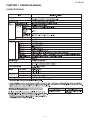
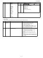
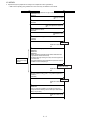
MODIFIED PARTS LIST
Ref.No.
Description
LC-32D42U/37D42U
(Base Model)
LC-42D43U
Remark
PRINTED WIRING BOARD ASSEMBLIES
R/C, LED Unit
DUNTKD909FM02
DUNTKD909FM02
No Change
KEY Unit
DUNTKD910FM02
DUNTKD910FM02
No Change
AV TERMINAL Unit
DUNTKD999FM04
DUNTKD935FM03
Change
MAIN Unit
DUNTKD862FM04
DUNTKD862FM04
Change
POWER Unit
RDENCA198WJQZ
RDENCA266WJQZ
Unit Replacement Item
LCD PANEL (NOTE: THE PARTS HERE SHOWN ARE SUPPLIED AS AN ASSEMBLY BUT NOT INDEPENDENTLY.)
32" LCD Panel
R1LK315T3LZ4BX
Delete
37" LCD Panel
R1LK370T3LZ5BW
Delete
42" LCD Panel
RLCUCA122WJZZ
Add.
MAIN Unit
C1118
Capacitor 10 16V Ceramic
RC-KZA510WJPZY
RC-KZA237WJZZY
Change
C1311
Capacitor 10 16V Ceramic
RC-KZA510WJPZY
RC-KZA237WJZZY
Change
C1313
Capacitor 10 16V Ceramic
RC-KZA510WJPZY
RC-KZA237WJZZY
Change
C1403
Capacitor 10 16V Ceramic
RC-KZA510WJPZY
RC-KZA237WJZZY
Change
C1423
Capacitor 10 16V Ceramic
RC-KZA510WJPZY
RC-KZA237WJZZY
Change
C1426
Capacitor 10 16V Ceramic
RC-KZA510WJPZY
RC-KZA237WJZZY
Change
C1433
Capacitor 10 16V Ceramic
RC-KZA510WJPZY
RC-KZA237WJZZY
Change
C1437
Capacitor 10 16V Ceramic
RC-KZA510WJPZY
RC-KZA237WJZZY
Change
C1466
Capacitor 10 16V Ceramic
RC-KZA510WJPZY
RC-KZA237WJZZY
Change
C1467
Capacitor 10 16V Ceramic
RC-KZA510WJPZY
RC-KZA237WJZZY
Change
C1531
VCKYCZ1EF104ZY
Delete
C1536
RC-KZA115WJZZY
Delete
C2001
Capacitor 10 16V Ceramic
RC-KZA510WJPZY
RC-KZA237WJZZY
Change
D1303
Diode KDS4148U-RTK/P
VHD1SS355//-1Y
VHDKDS4148/-1Y
Change
D1311
Diode PDZ9.1B,115
RH-EXA485WJQZY
RH-EX0264TAZZY
Change
D1519
VHDRB521S30-1Y
Delete
D2003
RH-PXA018WJZZY
Delete
D8451
Diode KDS4148U-RTK/P
VHD1SS355//-1Y
VHDKDS4148/-1Y
Change
D9602
Zener Diode EX0256TA
RH-EXA089WJZZY
RH-EX0256TAZZY
Change
D9606
Diode KDS4148U-RTK/P
VHD1SS352//-1Y
VHDKDS4148/-1Y
Change
D9607
Zener Diode EX0256TA
RH-EXA089WJZZY
RH-EX0256TAZZY
Change
D9701
Diode KDS4148U-RTK/P
VHD1SS352//-1Y
VHDKDS4148/-1Y
Change
D9702
Diode KDS4148U-RTK/P
VHD1SS352//-1Y
VHDKDS4148/-1Y
Change
D9703
Diode PDZ3.3B,115
RH-EX0253TAZZY
Add.
FB2604
Balun BLN-A206WJ
RBLN-0207TAZZY
RBLN-A206WJZZY
Change
FB9701
Balun BLN-0236TA
RBLN-0237TAZZY
RBLN-0236TAZZY
Change
IC1503
IC LVC2G14G-1
VHiN74LVC14-1Y
VHiLVC2G14G-1Y
Change
IC1504
VHiT7WH123U-1Y
Delete
IC2003
IC HC2G66DP-1
VHiTC7W66U/-1Y
VHiHC2G66DP-1Y
Change
IC2006
IC AHC32PW
VHiTCVHC32T-1Y
VHiAHC32PW+-1Y
Change
IC3302
IC TAR5SB25
VHiPQ1X251M-1Y
VHiTAR5SB25-1Y
Change
IC3304
IC S29GL064A90TFIR20H
VHiMST3586M-1Q
VHiMST3583M-1Q
Change
IC8701
IC TAR5SB33-1
VHiPQ1X331M-1Y
VHiTAR5SB33-1Y
Change
P1401
QPLGN0055CEZZY
Delete
P2001
QPLGN0060CEZZY
Delete
P2601
Plug
QPLGNA522WJQZY
QPLGNA493WJZZY
Change
P8401
QPLGN0060CEZZY
Delete
P9101
QPLGN0060CEZZY
Delete
P9202
QPLGNA144WJZZY
Delete
P9301
QCNCWA562WJQZY
Delete
Q1524
Transistor RT1N141U-T111-1
VSRT1N141U/-1Y
Add.
Q1525
Transistor KTA1535T-RTK/P
VSKTA1535T+-1Y
Add.
Q2001
VSKRC404E++-1Y
Delete
i
LC-42D43U
Ref.No.
Q8452
R1170
R1176
R1401
R1402
R1403
R1412
R1511
R1513
R1521
R1522
R1523
R1524
R1531
R1597
R1599
R1609
R1614
R2012
R2013
R2017
R2030
R2039
R2040
R2041
R2069
R2254
R2255
R2256
R2259
R2261
R2263
R2264
R2629
R2630
R2631
R3307
R3323
R3324
R8144
R8162
R8163
R8164
R8169
R8170
R8197
R8198
R8199
R8454
R8455
R8701
R8702
R8709
R8729
R9007
R9116
R9201
R9205
R9209
R9306
R9614
R9712
R9713
SC1503
Description
Transistor KTA1298Y
Resistor 10k 1/16W Metal Oxide
Resistor 330 1/16W Metal Oxide
Resistor 4.7k 1/16W Metal Oxide
Resistor 0 1/16W Metal Oxide
Resistor 0 1/16W Metal Oxide
Resistor 0 1/16W Metal Oxide
Resistor
Resistor
Resistor
Resistor
Resistor
Resistor
Resistor
Resistor
Resistor
47
47
47
47
47
47
47
47
47
1/16W
1/16W
1/16W
1/16W
1/16W
1/16W
1/16W
1/16W
1/16W
Metal Oxide
Metal Oxide
Metal Oxide
Metal Oxide
Metal Oxide
Metal Oxide
Metal Oxide
Metal Oxide
Metal Oxide
Resistor 4.7k 1/16W Metal Oxide
Resistor 3.9k 1/16W Metal Oxide
Socket
LC-32D42U/37D42U
(Base Model)
VS2SA1362GR-1Y
VRS-CZ1JF000JY
VRS-CZ1JF000JY
VRS-CJ1JF101JY
VRS-CZ1JF101JY
VRS-CZ1JF000JY
VRS-CZ1JF000JY
VRS-CZ1JF330JY
VRS-CZ1JF102FY
VRS-CZ1JF000JY
VRS-CZ1JF223FY
VRS-CZ1JF101JY
VRS-CZ1JF103FY
VRS-CZ1JF330JY
VRS-CZ1JF472JY
VRS-CZ1JF472JY
VRS-CZ1JF000JY
VRS-CZ1JF000JY
VRS-CZ1JF000JY
VRS-CZ1JF000JY
VRS-CZ1JF000JY
VRS-CZ1JF000JY
VRS-CZ1JF152JY
VRS-CZ1JF000JY
VRS-CZ1JF000JY
VRS-CZ1JF000JY
VRS-CZ1JF000JY
VRS-CZ1JF000JY
VRS-CZ1JF000JY
VRS-CZ1JF000JY
VRK-CD1JJ000JY
VRK-CD1JJ000JY
VRK-CD1JJ000JY
VRS-CZ1JF000JY
VRS-CZ1JF000JY
VRS-CZ1JF000JY
VRK-CD1JJ470JY
VRK-CD1JJ470JY
VRK-CD1JJ470JY
VRK-CD1JJ470JY
VRK-CD1JJ470JY
VRK-CD1JJ470JY
VRK-CD1JJ470JY
VRK-CD1JJ470JY
VRK-CD1JJ470JY
VRK-CD1JJ000JY
VRK-CD1JJ000JY
VRK-CD1JJ000JY
VRS-CH1JF000JY
VRS-CH1JF000JY
VRS-CZ1JF000JY
VRK-CD1JJ000JY
VRS-CZ1JF470JY
VRS-CZ1JF000JY
VRS-CZ1JF470JY
VRS-CZ1JF103JY
VRS-CZ1JF100JY
VRS-CZ1JF183FY
VRS-CZ1JF333JY
QSOCNA101WJN1
ii
LC-42D43U
VSKTA1298Y+-1Y
VRS-CZ1JF103FY
VRS-CZ1JF331JY
VRS-CZ1JF472JY
VRS-CK1JJ000JY
VRS-CK1JJ000JY
VRS-CK1JJ000JY
VRS-CK1JJ470JY
VRS-CK1JJ470JY
VRS-CK1JJ470JY
VRS-CK1JJ470JY
VRS-CK1JJ470JY
VRS-CK1JJ470JY
VRS-CK1JJ470JY
VRS-CK1JJ470JY
VRS-CK1JJ470JY
VRS-CZ1JF472JY
VRS-CZ1JF392JY
QSOCNA004WJZZ
Remark
Add.
Delete
Delete
Delete
Delete
Delete
Delete
Delete
Delete
Delete
Delete
Delete
Delete
Delete
Add.
Add.
Delete
Delete
Delete
Delete
Delete
Delete
Delete
Delete
Delete
Add.
Delete
Delete
Delete
Delete
Delete
Delete
Delete
Change
Change
Change
Delete
Delete
Delete
Change
Change
Change
Change
Change
Change
Change
Change
Change
Delete
Delete
Delete
Delete
Delete
Delete
Add.
Delete
Delete
Delete
Delete
Delete
Delete
Change
Delete
Change
LC-42D43U
Ref.No.
TU1101
Description
Tuner
LC-32D42U/37D42U
(Base Model)
RTUDAA007WJQZ
AV TERMINAL Unit
Refer to Parts List.
CABINET PARTS
Refer to Parts List.
SUPPLIED ACCESSORIES
Refer to Parts List.
PACKING PARTS
Refer to Parts List.
SERVICE JIGS
Refer to Parts List
iii
LC-42D43U
RTUDAA018WJQZ
Remark
Change
LC-42D43U
LC-42D43U
SAFETY PRECAUTION
Service Manual
IMPORTANT SERVICE SAFETY PRECAUTION
Service work should be performed only by qualified service technicians who are thoroughly familiar with all safety checks and the
servicing guidelines which follow:
WARNING
•
1. For continued safety, no modification of any circuit should be
attempted.
Use an AC voltmeter having with 5000 ohm per volt, or higher, sensitivity or measure the AC voltage drop across the resistor.
•
Connect the resistor connection to all exposed metal parts having a
return to the chassis (antenna, metal cabinet, screw heads, knobs
and control shafts, escutcheon, etc.) and measure the AC voltage
drop across the resistor.
2. Disconnect AC power before servicing.
All checks must be repeated with the AC cord plug connection
reversed. (If necessary, a nonpolarized adaptor plug must be used
only for the purpose of completing these checks.)
C A U T I O N : F O R C O N T I N U E D PROTECTION
AGAINST A RISK OF FIRE REPLACE ONLY WITH
SAME TYPE FUSE.
Any reading of 0.75 Vrms (this corresponds to 0.5 mA rms AC.) or
more is excessive and indicates a potential shock hazard which
must be corrected before returning the monitor to the owner.
F701 (250V 8A)
DVM
AC SCALE
BEFORE RETURNING THE RECEIVER (Fire &
Shock Hazard)
1.5k ohm
10W
Before returning the receiver to the user, perform the following
safety checks:
3. Inspect all lead dress to make certain that leads are not pinched,
and check that hardware is not lodged between the chassis and
other metal parts in the receiver.
0.15 μF
TEST PROBE
4. Inspect all protective devices such as non-metallic control knobs,
insulation materials, cabinet backs, adjustment and compartment
covers or shields, isolation resistor-capacitor networks, mechanical
insulators, etc.
5. To be sure that no shock hazard exists, check for leakage current in
the following manner.
•
Plug the AC cord directly into a 120 volt AC outlet.
•
Using two clip leads, connect a 1.5k ohm, 10 watt resistor paralleled by a 0.15μF capacitor in series with all exposed metal cabinet
parts and a known earth ground, such as electrical conduit or electrical ground connected to an earth ground.
TO EXPOSED
METAL PARTS
CONNECT TO
KNOWN EARTH
GROUND
///////////////////////////////////////////////////////////////////////////////////////////////////////////////////////////////////////////////////////////////////////////////////////////////////////////////////////////////////////////
SAFETY NOTICE
Many electrical and mechanical parts in LCD color television have
special safety-related characteristics.
For continued protection, replacement parts must be identical to those
used in the original circuit.
These characteristics are often not evident from visual inspection, nor
can protection afforded by them be necessarily increased by using
replacement components rated for higher voltage, wattage, etc.
The use of a substitute replacement parts which do not have the same
safety characteristics as the factory recommended replacement parts
shown in this service manual, may create shock, fire or other hazards.
Replacement parts which have these special safety characteristics are
identified in this manual; electrical components having such features
are identified by "
" and shaded areas in the Replacement Parts
List and Schematic Diagrams.
///////////////////////////////////////////////////////////////////////////////////////////////////////////////////////////////////////////////////////////////////////////////////////////////////////////////////////////////////////////
iv
LC-42D43U
PRECAUTIONS A PRENDRE LORS DE LA REPARATION
Ne peut effectuer la réparation qu' un technicien spécialisé qui s'est parfaitement accoutumé à toute vérification de sécurité et aux
conseils suivants.
AVERTISSEMENT
• A l'aide de deux fils à pinces, brancher une résistance de 1.5 kΩ
10 watts en parallèle avec un condensateur de 0.15μF en série
avec toutes les pièces métalliques exposées du coffret et une terre
connue comme une conduite électrique ou une prise de terre
branchée à la terre.
1. N'entreprendre aucune modification de tout circuit. C'est dangereux.
2. Débrancher le récepteur avant toute réparation.
• Utiliser un voltmètre CA d'une sensibilité d'au moins 5000Ω/V pour
mesurer la chute de tension en travers de la résistance.
PRECAUTION: POUR LA PROTECTION CONTINUE CONTRE LES RISQUES D'INCENDIE,
REMPLACER LE FUSIBLE
• Toucher avec la sonde d'essai les pièces métalliques exposées qui
présentent une voie de retour au châssis (antenne, coffret métallique, tête des vis, arbres de commande et des boutons, écusson,
etc.) et mesurer la chute de tension CA en-travers de la résistance.
Toutes les vérifications doivent être refaites après avoir inversé la
fiche du cordon d'alimentation. (Si nécessaire, une prise
d'adpatation non polarisée peut être utilisée dans le but de terminer ces vérifications.)
La tension de pointe mesurèe ne doit pas dépasser 0.75V (correspondante au courant CA de pointe de 0.5mA).
Dans le cas contraire, il y a une possibilité de choc électrique qui
doit être supprimée avant de rendre le récepteur au client.
F701 (250V 8A)
VERIFICATIONS CONTRE L'INCEN-DIE ET LE
CHOC ELECTRIQUE
Avant de rendre le récepteur à l'utilisateur, effectuer les vérifications suivantes.
3. Inspecter tous les faisceaux de câbles pour s'assurer que les fils
ne soient pas pincés ou qu'un outil ne soit pas placé entre le châssis et les autres pièces métalliques du récepteur.
DVM
ECHELLE CA
4. Inspecter tous les dispositifs de protection comme les boutons de
commande non-métalliques, les isolants, le dos du coffret, les couvercles ou blindages de réglage et de compartiment, les réseaux
de résistancecapacité, les isolateurs mécaniques, etc.
1.5k ohm
10W
5. S'assurer qu'il n'y ait pas de danger d'électrocution en vérifiant la
fuite de courant, de la facon suivante:
•
0.15 μF
SONDE D'ESSAI
Brancher le cordon d'alimentation directem-ent à une prise de courant de 120V. (Ne pas utiliser de transformateur d'isolation pour
cet essai).
AUX PIECES
METALLIQUES
EXPOSEES
BRANCHER A UNE
TERRE CONNUE
/////////////////////////////////////////////////////////////////////////////////////////////////////////////////////////////////////////////////////////////////////////////////////////////////////////////////////////////////////////////
AVIS POUR LA SECURITE
Pour assurer la protection, ces pièces doivent être identiques à celles
utilisées dans le circuit d'origine. L'utilisation de pièces qui n'ont pas
les mêmes caractéristiques que les pièces recommandées par l'usine,
indiquées dans ce manuel, peut provoquer des électrocutions, incendies, radiations X ou autres accidents.
De nombreuses pièces, électriques et mécaniques, dans les téléviseur ACL présentent des caractéristiques spéciales relatives à la sécurité, qui ne sont souvent pas évidentes à vue. Le degré de protection ne peut pas être nécessairement augmentée en utilisant des
pièces de remplacement étalonnées pour haute tension, puissance,
etc.
Les pièces de remplacement qui présentent ces caractéristiques sont
identifiées dans ce manuel; les pièces électriques qui présentent ces
particularités sont identifiées par la marque " " et hachurées dans la
liste des pièces de remplacement et les diagrammes schématiques.
/////////////////////////////////////////////////////////////////////////////////////////////////////////////////////////////////////////////////////////////////////////////////////////////////////////////////////////////////////////////
v
LC-42D43U
CHAPTER 1. OPERATION MANUAL
LC-42D43U
Service Manual
[1] SPECIFICATIONS
1–1
LC-42D43U
[2] OPERATION MANUAL
1–2
LC-42D43U
1–3
LC-42D43U
1–4
LC-42D43U
1–5
LC-42D43U
1–6
LC-42D43U
1–7
LC-42D43U
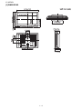
[3] DIMENSIONS
1–8
LC-42D43U
Service
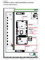
CHAPTER 2. REMOVING OF MAJOR PARTS
LC-42D43U
Manual
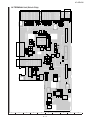
[1] REMOVING OF MAJOR PARTS
1. Remove the SD Card Cover.
2. Remove the 4 lock screws and detach the Stand Base Ass'y.
3. Remove the 12 lock screws, 5 lock screws and detach the Rear Cabinet.
3
1
SD Card Cover
3
2
Rear Cabinet
Stand Base Ass'y
2–1
LC-42D43U
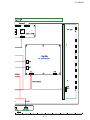
4. Remove the 4 lock screws and detach the Chassis Fixing Angle.
5. Remove the 4 lock screws and detach the Center Angle (L)(R).
6. Remove the 2 lock screws and detach the Stand Assist Angle.
7. Remove the 2 lock screws and detach the Stand Assist Cover.
8. Remove the 4 lock screws and detach the Stand Fixing Angle.
9. Remove the 7 lock screws, detach the MAIN Shield.
5
9
Center Angle (L)
Center Angle (R)
5
MAIN Shield
Stand Fixing Angle
8
Chassis Fixing Angle
Stand Assist Cover
6
7
4
Stand Assist Angle
4
2–2
LC-42D43U
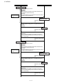
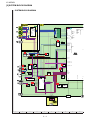
10.Disconnect all the connectors from all the PWBs.
11.Remove the Top Cover Ass'y. Remove the 1 lock screw from the Top Cover Ass'y and detach the KEY Unit.
Top Cover Ass'y
KEY Unit
11
10
10
10
10
2–3
LC-42D43U
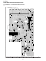
12.Remove the 7 lock screws and detach the Tray Chassis.
13.Remove the 2 lock screws, 3 lock screws, 2 lock screws, 2 hexagonal shaft for D-sub and detach the Terminal Angle.
14.Remove the 7 lock screws and detach the POWER Unit.
15.Remove the 4 lock screws and detach the TERMINAL Unit.
16.Remove the 5 lock screws, 3 rivet and detach the Heat Sink and MAIN PWB.
17.Remove the 2 lock screws and detach the Speaker (L)(R).
18.Detach the R/C, LED Unit.
16
14
16
MAIN PWB
Heat Sink
16
13
MA FC SA
13
12
POWER Unit
Tray Chassis
13
13
Terminal Angle
TERMINAL Unit
15
Speaker (R)
Speaker (L)
17
18
R/C, LED Unit
2–4
17
LC-42D43U
19.Remove the 4 lock screws and detach the Tray Fixing Angle (L)(R).
20.Remove the 7 lock screws and detach the Lug Angle Top.
21.Remove the 9 lock screws and detach the Lug Angle Bottom.
22.Remove the LCD Panel Module.
Lug Angle Top
20
20
20
20
20
19
19
Tray Fixing Angle (R)
19
21
21
21
Tray Fixing Angle (L)
21
21
19
21
21
Lug Angle Bottom
2–5
LC-42D43U
CHAPTER 3. ADJUSTMENT
LC-42D43U
Service Manual
[1] ADJUSTMENT PROCEDURE
The adjustment values are set to the optimum conditions at the factory before shipping. If a value should become improper or an adjustment is
required due to part replacement, make an adjustment according to the following procedure.
1. After replacement of any PWB unit and/or IC for repair, please note the following.
When replacing the following units, make sure to prepare the new units loaded with updated software.
MAIN Unit: DUNTKD862FM04.
AV TERMINAL Unit: DUNTKD935FM03
2. Signal Adjustment
2.1. White balance adjustment
1
2
Adjustment item
Setting
Automatic adjustment execution
Adjustment conditions
[Command]
Process mode
KRSW0001
KKT10037
Setting
KYOF0000
OSDS0001
SBSL0016
Multi-point adjustment
mode
MSET0001
Adjustment value initialization
MSET0004
Point 6
LEV60230
(WBI60920)
MG6G****
MG6B****
MG6R****
Point 5
LEV50215
(WBI50860)
MG5G****
MG5B****
MG5R****
Point 4
LEV40184
(WBI40736)
MG4G****
MG4B****
MG4R****
Point 3
LEV30128
(WBI30512)
MG3G****
Adjustment procedure
For detailed adjustment procedure, refer to “Kameyama Model Integral Monitor WB
Adjustment Specifications V1.4”.
1) Make the following settings for the set.
AV MODE: [DYNAMIC]
Backlight: +16
Aging time: Min. 60 minutes
2) Connect the white balance adjustment tool to the set.
[Adjustment procedure]
1) Using the remote controller, transmit the “monitor adjustment process” code.
2) Set the 6th point to the specified gradation level. With the strongest color being fixed,
turn down the R, G and B settings to their reference levels.
3) Set the 5th point to the specified gradation level. Correct the G setting (860 x 6thpoint G setting / 920) (rounded off), and make the R and B settings to their reference
levels.
4) Set the 4th point to the specified gradation level. Correct the G setting (736 x 6thpoint G setting / 920) (rounded off), and make the R and B settings to their reference
levels.
5) Set the 3rd point to the specified gradation level. Correct the G setting (512 x 6thpoint G setting / 920) (rounded off), and make the R and B settings to their reference
levels.
6) Set the 2nd point to the specified gradation level. Correct the G setting (256 x 6thpoint G setting / 920) (rounded off), and make the R and B settings to their reference
levels.
7) Set the 1st point to the specified gradation level. Correct the G setting (192 x 6thpoint G setting / 920) (rounded off), and make the R and B settings to their reference
levels.
8) With the MSET0003 command, write the adjustment values and turn off the AC
power.
* Initial R, G and B settings at point 6: Gradation level set at 920
* Initial R, G and B settings at points 1 thru 5: Corrected G setting at each point
(This is because the adjustment is made to achieve the same remainder of RGB setting /
4 at each point.)
[Adjustment value]
•As per the “standard set” submitted by Engineering Department
“LC-46D43U” Teaching set
[Adjustment reference] Instrument: Minolta CA-210 Engineering instrument
Point 6
Level
980
Point 5
928
Point 4
828
Point 3
568
Point 2
484
3–1
Reference
X=0.272
y=0.277
X=0.272
y=0.277
X=0.272
y=0.277
X=0.272
y=0.277
X=0.272
y=0.277
Adj. spec
±0.0025
Ins. spec
±0.0050
±0.0025
±0.0050
±0.0035
±0.0070
±0.0050
±0.0100
±0.0080
±0.0150
LC-42D43U
Adjustment item
Adjustment conditions
MG3B****
MG3R****
Point 1
Adjustment procedure
X=0.272
±0.0110
y=0.277
Set conditions for inspection
AV MODE: [DYNAMIC] (Reset)
Monochrome: ON
Black: OFF
Color Temp: High
Back Light: +16
Aging Time: Min. 60 minutes
216
Note
Point 2
LEV20064
(WBI20256)
MG2G****
MG2B****
MG2R****
Point 1
LEV10048
(WBI10192)
MG1G****
MG1B****
MG1R****
±0.0200
Writing
MSET0003
2.2. Key writing
1. EDID writing (Main PWB: QPWBXD862WJN2, analog RGB input terminal / HDMI input terminal)
1
2
Adjustment item
Analog RGB
EDID writing
Adjustment conditions
File version checking
HDMI EDID writing
Inspection mode
File version checking
Adjustment procedure
1) Using the checker, write the EDID data for HDMI to
IC1505 that is mounted on the main PWB.
TL1514: I2C clock, TL1515: I2C data
TL1516: 5V, TL1517: GND
TL1502: VCLK (Write: H, Read: V pulse)
2) In the analog RGB inspection, use a DDC-compatible
device. If the EDID has not been written, the analog
RGB input does not function normally.
1) Using the checker, write the analog HDMI EDID data to
IC1501 and IC1502 that are mounted on the main PWB.
TL1508/1510: I2C clock, TL1509/1511: I2C data
TL1512/1513: 5V, TL1519/1518: GND
TL1534/1535: Write protection (H: Write, L: Write
enable)
2) Write the data before the HDMI inspection with the
checker.
In the HDMI inspection, use a DDC-compatible device. If
the EDID has not been written, the HDMI does not function normally.
3–2
LC-42D43U
2. Adjustment sequence (adjustment according to the G adjustment value of gradation 6)
*
Make sure the adjusting point gradations are correct since they are different for each model.
PC
Set the light level to MAX with the light control command
(SBSL0016 for 45).
SBSL0016
Set
Setting is complete.
OK
Multi point adjustment mode setting
MSET0001
Multi point adjustment mode is set.
OK
Initialize adjustment values.
MSET0004
Initialization is done.
OK
Adjustment gradation setting (point 6 = 230 gradation adjustment*)
LEV60230
(WBI60920
Pattern display
Adjustment values are set.
OK
Repeat until RGB
become the target
values.
Adjust RGB to the target xy values.
MG6RXXXX
MG6GXXXX
MG6BXXXX
* XXXX indicates the adjusted values between 0000 and 1023
(4 digit decimal number with zero fill).
* In order to adjust by reducing the value, set the strongest color
as the fixed color.
* The default adjustment value of RGB is the parameter value of
the WBI6 command multiplied by 2.
The adjustment value is
reflected in the image.
Adjustment values are set.
OK
Adjustment gradation setting (point 5 = 215 gradation adjustment*)
LEV50215
(WBI50860)
Pattern display
Adjustment values are set.
OK
Correction of G value
MG5GXXXX
When G is changed at gradation 6, calculate the ratio of the
change and set the following value to XXXX: (the value set with
WBI5) x 2 x (the ratio).
Adjustment values are set.
OK
3–3
LC-42D43U
PC
Set
Start measurement
Repeat until RGB
become the target
values.
Adjust RB to the target xy values.
MG5RXXXX
MG5BXXXX
* XXXX indicates the adjusted values between 0000 and 1023
(4 digit decimal number with zero fill).
* G is fixed.
* The default adjustment value of RGB is the parameter value
of the WBI5 command multiplied by 2.
The adjustment value is
reflected in the image.
Adjustment values are set.
OK
Adjustment gradation setting (point 4 = 184 gradation adjustment*)
LEV40184
(WBI40736)
Pattern display
Adjustment values are set.
OK
Correction of G value
MG4GXXXX
When G is changed at gradation 6, calculate the ratio of the
change and set the following value to XXXX: (the value set with
WBI4) x 2 x (the ratio).
Adjustment values are set.
OK
Start measurement
Repeat until RGB
become the target
values.
Adjust RB to the target xy values.
MG4RXXXX
MG4BXXXX
* XXXX indicates the adjusted values between 0000 and 1023
(4 digit decimal number with zero fill).
* G is fixed.
* The default adjustment value of RGB is the parameter value of
the WBI4 command multiplied by 2.
The adjustment value is
reflected in the image.
Adjustment values are set.
OK
Adjustment gradation setting (point 3 = 128 gradation adjustment*)
LEV30128
(WBI30512)
Pattern display
Adjustment values are set.
OK
Correction of G value
MG3GXXXX
When G is changed at gradation 6, calculate the ratio of the
change and set the following value to XXXX: (the value set with
WBI3) x 2 x (the ratio).
Adjustment values are set.
OK
3–4
LC-42D43U
PC
Set
Start measurement
Repeat until RGB
become the target
values.
Adjust RB to the target xy values.
MG3RXXXX
MG3BXXXX
* XXXX indicates the adjusted values between 0000 and 1023
(4 digit decimal number with zero fill).
* G is fixed.
* The default adjustment value of RGB is the parameter value of
the WBI3 command multiplied by 2.
The adjustment value is
reflected in the image.
Adjustment values are set.
OK
Adjustment gradation setting (point 2 = 64 gradation adjustment*)
LEV20064
(WBI20256)
Pattern display
Adjustment values are set.
OK
Correction of G value
MG2GXXXX
When G is changed at gradation 6, calculate the ratio of the
change and set the following value to XXXX: (the value set with
WBI2) x 2 x (the ratio).
Adjustment values are set.
OK
Start measurement
Repeat until RGB
become the target
values.
Adjust RB to the target xy values.
MG2RXXXX
MG2BXXXX
* XXXX indicates the adjusted values between 0000 and 1023
(4 digit decimal number with zero fill).
* G is fixed.
* The default adjustment value of RGB is the parameter value of
the WBI2 command multiplied by 2.
The adjustment value is
reflected in the image.
Adjustment values are set.
OK
Adjustment gradation setting (point 1 = 48 gradation adjustment*)
LEV10048
(WBI10192)
Pattern display
Adjustment values are set.
OK
Correction of G value
MG1GXXXX
When G is changed at gradation 6, calculate the ratio of the
change and set the following value to XXXX: (the value set with
WBI1) x 2 x (the ratio).
Adjustment values are set.
OK
3–5
LC-42D43U
PC
Set
Start measurement
Repeat until RGB
become the target
values.
Adjust RB to the target xy values.
MG1RXXXX
MG1BXXXX
* XXXX indicates the adjusted values between 0000 and 1023
(4 digit decimal number with zero fill).
* G is fixed.
* The default adjustment value of RGB is the parameter value of
the WBI1 command multiplied by 2.
The adjustment value is
reflected in the image.
Adjustment values are set.
OK
Writing of adjusted values
MSET0003
Writing is complete.
OK
Deleting adjustment patterns
MSET0000
Deletion is complete.
OK
Completion of adjustment
2.3. Menu list in process A mode
Page
4
Line
Item
TUNER VCHIP TEST (69ch)
TUNER VCHIP TEST (7ch)
TUNER VCHIP TEST (4ch)
TUNER VCHIP TEST (10ch)
TUNER VCHIP TEST (15ch)
Explanation
Execute TUNER TEST
3–6
L C -4 2 D 4 3 U
Service
CHAPTER 4. TROUBLESHOOTING TABLE
LC-42D43U
Manual
[1] TROUBLESHOOTING TABLE
No audio output during UHF/VHF reception
Is SIF output from the tuner (TU1101_Pin15) normal?
NO
Check the tuner and peripheral circuits.
YES
Is input signal fed to pin 21 of IC1401 (SIF Demodulator) normal?
NO
Check the filter circuits (Q1102-3) and peripheral circuits.
NO
Check between pins 29 and 30 of IC1401 and pins 51 and 52 of
IC1404 (CODEC).
NO
Are the DSP_LRCK, DSP_BCKIN, DSP_SDIN1, DSP_MCLK,
DSP_SDOUT1, DSP_SDOUT2 signals sent from IC1404 to
IC1407 (DSP) normally?
YES
Are audio signals from pins 29 and 30 of IC1401 to pins 51 and
52 of IC1404 (CODEC) normal?
YES
Are audio outputs of pins 38 and 39 of IC1404 normal?
YES
Check IC1404 and peripheral circuits.
YES
Is audio input from pins 38 and 39 of IC1404 to pins 3 and 5 of
IC2701(STEREO_AMP) normal?
YES
Is audio output from IC2701 normal?
NO
Check the circuits between pins 38 and 39 of IC1404 and pins 3
and 5 of IC2701. (MUTE circuits: Q1307, Q1314, Q1313)
NO
Check IC2701 and peripheral circuits.
YES
Check the connector (P2703) of TERMINAL_UNIT and around
the speakers.
No monitor audio output
Is monitor audio output set to “Variable”?
YES
Reset monitor audio output to “Fixed”.
NO
Are audio output pins 40 and 41 of IC1404 (CODEC) normal?
NO
Check IC1404 and peripheral circuits.
YES
Are audio output pins 7 and 1 of IC1408 (Buffer_AMP) normal?
NO
Check IC1408 and peripheral circuits.
YES
Check between IC1408 and MONITOR OUTPUT terminal (J502).
4–1
LC-42D43U
No audio output from external input
<<HDMI>> [INPUT-4/INPUT5 (Digital audio mode)]
Is digital audio signal (DTV_SPDIF) fed from pin E12 of IC8101 to pin 4 of IC1404?
<<HDMI>> [INPUT-5 (Analog audio mode)]
Is L-ch audio signal fed from pin 3 of input terminal J1501 to pin 57 of IC1404?
Is R-ch audio signal fed from pin 2 of input terminal J1501 to pin 58 of IC1404?
PCINPUT<<INPUT-6>>
Is L-ch audio signal fed from pin 2 of input terminal J1502 to pin 55 of IC1404?
Is R-ch audio signal fed from pin3 of input terminal J1502 to pin 56 of IC1404?
<<INPUT-1>>
Is L-ch audio signal fed from input terminal J501 to pin 12 of IC1405?
Is R-ch audio signal fed from input terminal J501 to pin 1 of IC1405?
<<INPUT-2>>
<<INPUT-3>>
Is L-ch audio signal fed from input terminal J502 to pin 14 of IC1405?
Is L-ch audio signal fed from input terminal J501 to pin 15 of IC1405?
Is R-ch audio signal fed from input terminal J502 to pin 5 of IC1405?
Is R-ch audio signal fed from input terminal J501 to pin 2 of IC1405?
Is L-ch audio fed from pin 13 of IC1405 to pin 53 of IC1404?
Is R-ch audio fed from pin 3 of IC1405 to pin 54 of IC1404?
YES
No audio output during digital broadcasting reception
Are the I2S signals DAKCK, SCLK, LRCK, and
DATAOUT sent from pins B22, F13, E13 and F12 of
IC8101 normally?
YES
Are input signals of pins 24 (DAKCK), 11 (SCLK), 10
(LRCK), 32 (DATA) of IC1404 normal?
YES
Are audio signals from pins 29 and 30 of IC1404 to pins 27 and
25 of IC1407 (DSP) normal?
YES
Are audio outputs pins 38 and 39 of IC1404 normal?
NO
Check around IC8101 BCM3551.
NO
Check the circuits between pins B22, F13, E13 and F12 of IC8101
and pins 24, 11, 10 and 32 of IC1404.
NO
Check between pins 29 and 30 of IC1404 and pins 27 and 25 of
IC1407 (DSP).
NO
Are the LRCK, BICK, SDTO and SDTI signals sent from IC1404 to
IC1407 (DSP) normally?
YES
Check IC1403 and peripheral circuits.
YES
Is audio input from pins 38 and 39 of IC1404 to pins 3 and 5 of
IC2701(STEREO_AMP) normal?
YES
Is audio output from IC2701 normal?
NO
Check the circuits between pins 38 and 39 of IC1404 and pins 3 and
5 of IC2701. (MUTE circuits: Q1307, Q1313, Q1314, Q1404)
NO
Check IC2701 and peripheral circuits.
YES
Check the connector (P2703) of TERMINAL_UNIT and around
the speakers.
4–2
LC-42D43U
<Component video signal input> No video output (1)
No video output from external input <<INPUT-1>>
Is INPUT-1 selected on the input switching menu screen?
Select INPUT-1 and the input signal on the input switching menu
screen.
NO
When INPUT-1 cannot be selected since the characters INPUT-1
on the menu screen are gray.
Is the video signal detection function normal?
Check between J501 and pin 70 of IC501.
YES
Is video signal fed to pin 65 of IC501 (AV SWITCH)?
NO
Check between J501 and pin 65 of IC501.
YES
Is video signal sent to pin 60 of IC501?
NO
Check IC501 (AV SWITCH) and peripheral circuits.
YES
Is video signal sent to pin 2 of TERMINAL_UNIT connector
(FC_SC501)?
NO
Check between IC501 and SC501. (Q501, Q502, etc.)
YES
Is video signal fed to pin 2 of MAIN_UNIT connector
(FC_SC1101)?
NO
Check the board-to-board cable “FC”.
YES
Is video signal fed to pin K25 of IC8101 (Broadcom) via L.P.F.
composed of Q2202 and Q2210?
NO
Check between IC501 and IC3301. (Q2202, Q2210, etc.)
YES
Are digital video (LVDS) signals sent from pins 37-42 and 45-48
of IC2602?
NO
Check IC2602 and peripheral circuits.
NO
Check IC8101 and peripheral circuits.
Are digital video (COMOS) signal sent from IC8101 (DVODATA 0
~ 23, DVOCLKO, DVODE, DVOHSYNC, DVOVSYNC)?
YES
Check LCD_CONTROL PWB.
4–3
LC-42D43U
<Component video signal input> No video output (2)
No video output from external input <<INPUT-2>>
Is INPUT-2 selected on the input switching menu screen?
Select INPUT-2 and the input signal on the input switching menu
screen.
NO
When INPUT-2 cannot be selected since the characters INPUT-2
on the menu screen are gray.
Is the video signal detection function normal?
Check between J502 and pin 76 of IC501.
YES
Is video signal fed to pin 71 of IC501 (AV SWITCH)?
NO
Check between J502 and pin 71 of IC501.
YES
Is video signal sent to pin 60 of IC501?
NO
Check IC501 (AV SWITCH) and peripheral circuits.
YES
Is video signal sent to pin 2 of TERMINAL_UNIT connector
(FC_SC501)?
NO
Check between IC501 and SC501. (Q501, Q502, etc.)
YES
Is video signal fed to pin 2 of MAIN_UNIT connector
(FC_SC1101)?
NO
Check the board-to-board cable “FC”.
YES
Is video signal fed to pin K25 of IC8101 (Broadcom) via L.P.F.
composed of Q2202 and Q2210?
NO
Check between IC501 and IC3301. (Q2202, Q2210, etc.)
YES
Are digital video (LVDS) signals sent from pins 37-42 and 45-48
of IC2602?
NO
Check IC2602 and peripheral circuits.
NO
Check IC8101 and peripheral circuits.
Are digital video (COMOS) signal sent from IC8101 (DVODATA 0
~ 23, DVOCLKO, DVODE, DVOHSYNC, DVOVSYNC)?
YES
Check LCD_CONTROL PWB.
4–4
LC-42D43U
<Composite video signal/S-video signal input> No video output (3)
No video output from external input <<INPUT-3>>
Is INPUT-3 selected on the input switching menu screen?
YES
Is signal fed to each input terminal of IC501 (AV SWITCH)?
<Composite video signal input>
Is video signal fed to pin 3 of IC501?
<S-video signal input>
Are Y and C signals fed to pins 5 and 7 of IC501 respectively?
YES
<Composite video signal input>
Is video signal sent to pin 60 of IC501?
<S-video signal input>
Are Y and C signals sent to pins 60 and 59 of IC501 respectively?
YES
<Composite video signal input>
Is video signal sent to pin 2 of TERMINAL_UNIT connector
(FC_SC501)?
<S-video signal input>
Are Y and C signals sent to pins 2 and 4 of TERMINAL_UNIT
connector (FC_SC501) respectively?
YES
<Composite video signal input>
Is video signal fed to pin 2 of MAIN_UNIT connector
(FC_SC1101)?
<S-video signal input>
Are Y and C signals fed to pins 2 and 4 of MAIN_UNIT connector
(FD_SC1101) respectively?
YES
<Composite video signal input>
Is video signal fed to pin K25 of IC8101 (Broadcom) via L.P.F.
composed of Q2202 and Q2210?
<S-video signal input>
Are Y and C signals fed to pins k25 and L24 of IC8101 (Broadcom) via L.P.F. composed of Q2202 and Q2210 and via L.P.F.
composed of Q2203 and Q2211 respectively?
YES
Are digital video (LVDS) signals sent from pins 37-42 and 45-48
of IC2602?
Are digital video (COMOS) signal sent from IC8101 (DVODATA 0
~ 23, DVOCLKO, DVODE, DVOHSYNC, DVOVSYNC)?
Select INPUT-3 and the input signal on the input switching menu
screen.
NO
When INPUT-3 cannot be selected since the characters INPUT-3
on the menu
Is the video signal detection function normal? Check between
J501 and pin 2 of IC501.
Is the S-video signal detection function normal? Check between
J503 and pin 42 of IC501.
NO
Check between J501 and pin 3 of IC501.
NO
Check between J503 and pins 5 and 7 of IC501.
NO
Check IC501 (AV SWITCH) and peripheral circuits.
NO
Check between IC501 and SC501. (Q501, Q502, Q503, Q504,
etc.)
NO
Check the board-to-board cable “FC”.
NO
Check between SC1101 and IC3301. (Q2202, Q2210, etc.)/
(Q2203, Q2211, etc.)
NO
Check IC2602 and peripheral circuits.
NO
Check IC8101 and peripheral circuits.
YES
Check LCD_CONTROL PWB.
4–5
LC-42D43U
<Component video signal input> No video output (4)
No video output from external input <<INPUT-1>>
Is INPUT-1 selected on the input switching menu screen?
NO
Select INPUT-1 and the input signal on the input switching menu
screen.
When INPUT-1 cannot be selected since the characters INPUT-1
on the menu screen are gray.
Is the component video signal detection function normal? Check
between 8 pin of J501 and pin 38 of IC501.
YES
Are component video signals fed to pins 21, 23 and 25 (Y, PB
and PR) of IC501(AV SWITCH)?
NO
Check between J501 and each input pin of IC501.
YES
Are Y, PB and PR signals sent to pins 60, 59 and 58 of IC501
respectively?
NO
Check IC501 and peripheral circuits.
YES
Are component video signals sent to pins 2, 4 and 6 of
TERMINAL_UNIT connector (FC_SC501)?
NO
Check between IC501 and SC501. (Q501-Q506, etc.)
YES
Are component video signals fed to pins 2, 4 and 6 of
MAIN_UNIT connector (FC_SC1101)?
NO
Check the board-to-board cable “FC”.
YES
Are Y, Pb and Pr signals fed to pins L26, J25, J26 of IC8101
(Broadcom) respectively?
NO
Check between SC1101 and IC8801. (Q2210, Q2211, Q2212,
etc.)
YES
Are digital video (LVDS) signals sent from pins 37-42 and 45-48
of IC2602?
NO
Check IC2602 and peripheral circuits.
NO
Check IC8101 and peripheral circuits.
Are digital video (COMOS) signal sent from IC8101 (DVODATA 0
~ 23, DVOCLKO, DVODE, DVOHSYNC, DVOVSYNC)?
YES
Check LCD_CONTROL PWB.
4–6
LC-42D43U
<Component video signal input> No video output (5)
No video output from external input <<INPUT-2>>
Is INPUT-2 selected on the input switching menu screen?
NO
Select INPUT-2 and the input signal on the input switching menu
screen.
When INPUT-2 cannot be selected since the characters INPUT-2
on the menu screen are gray.
Is the component video signal detection function normal? Check
between 8 pin of J502 and pin 40 of IC501.
YES
Are component video signals fed to pins 27, 29 and 31 (Y, PB
and PR) of IC501(AV SWITCH)?
NO
Check between J502 and each input pin of IC501.
YES
Are Y, PB and PR signals sent to pins 60, 59 and 58 of IC501
respectively?
NO
Check IC501 and peripheral circuits.
YES
Are component video signals sent to pins 2, 4 and 6 of
TERMINAL_UNIT connector (FC_SC501)?
NO
Check between IC501 and SC501. (Q501-Q506, etc.)
YES
Are component video signals fed to pins 2, 4 and 6 of
MAIN_UNIT connector (FC_SC1101)?
NO
Check the board-to-board cable “FC”.
YES
Are Y, Pb and Pr signals fed to pins L26, J25, J26 of IC8101
(Broadcom) respectively?
NO
Check between SC1101 and IC8801. (Q2210, Q2211, Q2212,
etc.)
YES
Are digital video (LVDS) signals sent from pins 37-42 and 45-48
of IC2602?
NO
Check IC2602 and peripheral circuits.
NO
Check IC8101 and peripheral circuits.
Are digital video (COMOS) signal sent from IC8101 (DVODATA 0
~ 23, DVOCLKO, DVODE, DVOHSYNC, DVOVSYNC)?
YES
Check LCD_CONTROL PWB.
4–7
LC-42D43U
No video output from HDMI input (INPUT4)
INPUT4
Are signals fed from HDMI (SC1501) connector to input terminals
H_RX0± (pins 70 and 71), H_RX1± (pins 73 and 74), H_RX2±
(pins 76 and 77) and H_RXC± (pins 67 and 68) of IC1507
(TMDS_SW)?
NO
Is IC1501 (E2PROM) accessed with I2C when connecting HDMI
device and is DDC_I2C_CLOCK/DATA data read out?
YES
NO
Check IC1501 and peripheral circuits.
Are cables connected securely?
Check the setting of HDMI device.
YES
Are signals fed from IC1507 (TMDS_SW) to input terminals
H_RX0± (pins B19 and A19), H_RX1± (pins A18 and B18),
H_RX2± (pins D18 and C18) and H_RXC± (pins C19 and D19)
of IC8101 (Broadcom)?
YES
Are digital video (LVDS) signals sent from pins 37-42 and 45-48
of IC2602?
Are digital video (COMOS) signal sent from IC8101 (DVODATA 0
~ 23, DVOCLKO, DVODE, DVOHSYNC, DVOVSYNC)?
NO
Check IC1507 (TMDS_SW) and peripheral circuits.
For INPUT4, pin 21 is Low and pin 22 is High.
NO
Check IC2602 and peripheral circuits.
NO
Check IC8101 and peripheral circuits.
YES
Check LCD_CONTROL PWB.
When using an old HDMI transmission device, some video formats cannot be selected or no sound is heard. Since this model conforms to the latest
HDMI standard, the HDMI transmission device does not recognize the data of the latest version correctly. It is necessary to upgrade its firmware.
Download the latest firmware from the web site of each manufacturer, or contact the customer service center of each manufacturer.
4–8
LC-42D43U
Service Manual
CHAPTER 5. OVERALL WIRING DIAGRAM/BLOCK
DIAGRAM
LC-42D43U
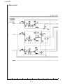
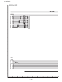
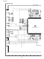
[1] OVERALL WIRING DIAGRAM
OVERALL WIRING DIAGRAM
,
+
*
)
(
'
&
%
$
#
5–1
LC-42D43U
5–2
LC-42D43U
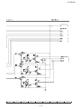
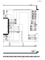
[2] SYSTEM BLOCK DIAGRAM
SYSTEM BLOCK DIAGRAM
,
/#+0
6'4/+0#.
+
8A#
+0276
*
%8$5.4
%QORQPGPV
;2D2T
%8$5.4
%8$5
8.4
%QORQPGPV
;2D2T
8KFGQ
8
;2D2T
8KFGQ
8
;2D2T
5&A.
5&A%
%
˴/*\
;
˴/*\
#PCNQI4)$
'&5#('A%8$5A
'&5#('A+(A2
'&5#('A+(A0
:
/*\
/56/
*&8&
&KIKVCN+0
&8+#=?
&8+%.&8+*5;0%
&8+85;0%
&8+&'
4)$DKV
%-*&8&&'
)
+%
#/2
%8$5
*&/+A+%
8
)#+0
8
&KUENGVG
$2( #8
#(6
7#
*&/+A%.-
8
5+(
/*\
9:)#
*&/+A#=?
/#5%
RKP
67
#PCNQI&KIKVCN
6WPGT
EJDKV
#&%
OWZEJ
/*\
K
8
8
+%
4)$#&%
.4
#WFKQ1WV
&KIKVCN1WV
&81#=? DKV&KI
&81%.-
&81%.-
&81&'
&81*5;0%
&8185;0%
&81&'
5&A24
%8$5
˴/*\
+(
/10+614
176
5&A2$
%T
˴/*\
EJDKV
#&%
OWZEJ
/*\
K
5&A;
%D
˴/*\
#8
&8
5&A%8$5
;
˴/*\
5
58KFGQ
%8$5
˴/*\
68
/CKP
1WV
176
+%
+%
&&4
&8 &8 &8
#8
&KUENGVG˴.2(
8KFGQ
8
;%
%8$5
8.4
%8$5.4
+0276
+%
#859+6%*
//:3
(%5%
RKP
+0276
%8$5
8.4
㪠㪚㪏㪈㪇㪈
㪙㪚㪤㪊㪌㪌㪈
+%
&#%
/(2
(
& +(
&KUENGVG
(KNVGT
#)%
+(A#)%
&5A#)%+A%6.
670A+%
6WPGT+%
+%
+%A -*\㨪8
+%
+%A -*\㨪8
*&/+
''241/
$4.(
#8
6/&5A5'.A&=?
4:AZ
&8
&8
''241/
+0276
*&/+
4:AZ
$78
&8
''241/
+0276
8&
4)$
&68A*&/++5
52&+(
&KIKVCN#WFKQ &6852&+(
4)$
+0276
4)$#WFKQ
/KPK2NWI
+0276
*&/+#WFKQ
+%
8QKEG/WNVKRNGZ&GEQTFGT
#05#
#68.4
8%4.4
4)$.4
*&/+.4
&8
+%
&52
6#5&
&8
+%
''241/
&52A5&176
&52A5&176
&52A5&+0
&68A52+&(
&68A+5
%
+0
:
:VCN
/*\
+%
%1&'%
#-'3 176
/*\
7#46
#8
#8
(QT*&%2
+%':6
+5A+0
+%
+1
/
/76'
*&8&
&
+%
''241/
$9,
&8
6Q5WD%27
+%
5JQV/WNVK
+%A -*\㨪8
+%
6/&5A5'.A%.-
+0
+0
+0
5&6+#
5&6+#
5&61#
+5A176
176
*2
6:
4'
75$
''241/
+0276
&8 +%
2%+.1%#.$75
&8
'
+%
#WFKQ59
6%$6
52A.52A4
*2A.*2A4
&8
+%
014(.#5*
/D
4:
2
%QPPGEVQTHQT
UQHVYCTGYTKVKPI
7#46
+%
6/&5
5GNGEVQT
6/&5#
&8
5&6+$
126+%#.
176
8
8
2
$75%QPPGEVGT
5#5% RKP
5%
75$
$
(QT'ZCO
+%
&KIKVCN#/2
62#&
6'4/+0#.
52
2
R
#
5–3
+%
%2.&
LC-42D43U
㧸㧯㧰
8
+%
+%
&&45&4#/
/DKV
&&4
((%
㪣㪚㪛
㪧㪘㪥㪜㪣
4.7&
5*2
RKP
20.8
6'/2=?15A5'6(4#/'
((%
+%
.8&56Z
8*+8#).(;
.82
R((%
&8
&KIKVCN1WV
&81#=? DKV&KIKVCN
&81%.-
&81%.-
&81&'
&81*5;0%
&8185;0%
&81&'
+%
4GUGV
8DTV
*A+%
+08A'44
$78
+%
''241/
$4.(
㧮㧸
6*
6JGTOKUVGT
ޣ.#ޤ
RKP
:
:VCN
/*\
ޣ.%ޤ
RKP
+08'46'4
㩷
ޣ.#ޤ
RKP
#(6
+08'46'4
㩷
ޣ.%ޤ
RKP
#&
#&
+1
ޣ.$ޤ
RKP
+06
54'5'6
+1
2
$QCTF%QPHKI
6*'4/1
#&
+%
5WD%27
/
7#46
59
2/A4'3
%$1165
㪇㪈
㪌㪌㪈
+%
$78
-*\
7#46
+%
&#%
/(2
59
+
.$2
RKP
8QP
&8
4%
$78
12%
$78
&8
+%
5&%VTN
6%#(
&8
5%
5&%#4&
/#+0
ޓ#8
ޓ#8
&ޓ8
&ޓ8
&ޓ8
&ޓ8
56$;A219
-';-';
5%
2&ޓ2
2+0
20.8
$CEM7R
ޓ$78
12%A.'&219A.'&A4219A.'&A)
2%+A#&=?'#=?'&=?
5%
75$
#%A&'6
219'4
54'5'6
75$
4'5'6
.'&
+%
%2.&
4%
2%+.1%#.$75
4'5'6
+06
(%.-
$78
#/28
8
2'
2*
2
2+0
&8
/*\
25A1020.219
&A219.+0-A219
&'6A8&'6A8
ޣ.#ޤ
R
219'4
8
$7
6'4/+0#.
-/2
RKP
4#ޓ2
R
#%
4#ޓ2
R
(QT'ZCOKPCVKQP
-';
.'&
㪧㪦㪮㪜㪩
㪠㪥㪧㪬㪫
㪚㪟㪄㪬㪧㪆㪛㪦㪮㪥
㪭㪦㪣㪄㪬㪧㪆㪛㪦㪮㪥
4%
12%
.'&
ޓ
5–4
LC-42D43U
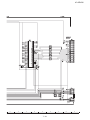
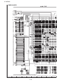
CHAPTER 6. PRINTED WIRING BOARD
LC-42D43U
Service Manual
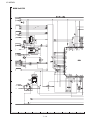
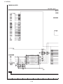
[1] AV TERMINAL UNIT PRINTED WIRING BOARD
AV TERMINAL Unit (Side-A)
J
I
H
G
F
E
D
C
B
A
1
2
3
4
5
6
6–1
7
8
9
10
LC-42D43U
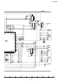
AV TERMINAL Unit (Side-A Chip)
J503
R532
D507
C519
R533
R534
C520
SC502
SC501
k001
R583
Q506
C553
LF1
D2702
D2703
R2724
P2704
R2722
C2733
R2723
C2742
C2734
L2702
L2701
C2741
C2718
LUG2702
D2701
C2717
C2709
C2706
C2745
R2706
R2704
C2711
C2720
R2701
C2747
C2716
R2703
R2702
R2705
FB519
C547
C546
R577
Q504
C552
P2703
C
IC2701
C2703
C2746
C2715
C2701
R2719
C2708
FB2704
C2707
C2710
C2714
C2725
R2713
C2731
C2726
R2714
10
9
8
C518
R594
R593
Q509
C554
R571
Q502
R575
R585
R581
C2744
B
D506
Q507
R591
C551
R569
R579
C502
R505
R503
Q508
R561
C568
R573
FB518
C522
R531
FB502
D508
R501
C501
C523
R568
R567
C542
C575
C2730
R617
FB532
C2705
R535
D502
R605
R536
R538
R610
R539
R559
C538
R615
P502
C2702
C2712
FB503
LUG502
D509
C521
D510
R540
R541
C564
C526
C527
C530
C529
R2720
Q511
FB534
C2704
C2713
D503
D501
FB501
R506
R504
R502
FB504 C558
C505
C504
C570
C506
C571
R510
FB505 R509
R508 R507
R511
C507
R513
C508
C569
D511
C528
R548
R549
R550
R7510
6–2
C2728
C2727
7
6
5
FB506
FB507 R512
C511
D504
C510
C509
C572
FB508 R515
R516
R514
FB509
R517
FB510
FB511
D505
C515
D515
C2737
R565
D516
FB2712
R2721
R600
C2732
C2739
D2706
FB2711
D2705
C2738
D2704
LUG2701
D2707
R613
R604
D517
FB531
R519
R526
C514
C7502
C7505
FB7506
R612
FL504
FB2709
FL502
R611
R518
C573
R520
FB515
R523
C513
C512
C516
C517
R616
FL501
C560
R614
R618
C559
C2740
FB533
R527
R524
C574
R522
R521
FB513
FB514
R525
R529
C2743
E
IC2702
FL503
L501
R619
R584
R582
C565
R578
R576
R572
R570
R574
Q501
R580
Q503
C566
C7506
R586
Q505
UNT501
FB2710
D
FB512
R528
R530
SC7501
C7501
C7507
IC7501
FB520
R542
C7504
C7503
F
D7504
R592
R7513
R7512
FB7503 R7515
R587
D7503
FB7501 R7518
C541
C557
FB7502 R7516
C555
R590
C524
R543
FB7504 R7517
R562
R588
D7505
C540
C567
R589
R558
R563
R602
D518
R564
R557
G
R607
C545
C556
C525
D7506
R609
C535
R601
C544
R603
C537
R556
D519
C536
C534
D512
D514 D513
R537
H
R566
IC501
R554
R555
R608
C533
4
3
2
1
FB516
FB517
LUG501
C532
C503
I
J501
J502
J
C543
L2704
C2729
L2703
A
LC-42D43U
— MEMO —
6–3
LC-42D43U
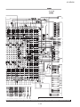
CHAPTER 7. SCHEMATIC DIAGRAM
LC-42D43U
Service Manual
[1] DESCRIPTION OF SCHEMATIC DIAGRAM
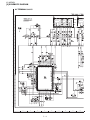
1. VOLTAGE MEASUREMENT CONDITION:
1) The voltages at test points are measured on exclusive AC adaptor
and the stable supply voltage of AC 120V. Signals are fed by a
color bar signal generator for servicing purpose and the above voltages are measured with a 20k ohm/V tester.
2. INDICATION OF RESISTOR & CAPACITOR:
RESISTOR
1) The unit of resistance "Ω" is omitted.
(K=kΩ=1000Ω, M=MΩ).
2) All resistors are ± 5%, unless otherwise noted.
(K= ± 10%, F= ± 1%, D= ± 0.5%)
3) All resistors are 1/16W, unless otherwise noted.
CAPACITOR
1) All capacitors are μF, unless otherwise noted.
(P=pF=μμF).
2) All capacitors are 50V, unless otherwise noted.
CAUTION:
This circuit diagram is original one, therefore there may be a slight
difference from yours.
SAFETY NOTES:
1) DISCONNECT THE AC PLUG FROM THE AC OUTLET
BEFORE REPLACING PARTS.
2) SEMICONDUCTOR HEAT SINKS SHOULD BE REGARDED AS
POTENTIAL SHOCK HAZARDS WHEN THE CHASSIS IS
OPERATING.
IMPORTANT SAFETY NOTICE:
PARTS MARKED WITH "
"(
) ARE IMPORTANT
FOR MAINTAINING THE SAFETY OF THE SET. BE SURE TO
REPLACE THESE PARTS WITH SPECIFIED ONES FOR MAINTAINING THE SAFETY AND PERFORMANCE OF THE SET.
AVIS DE SECURITE IMPORTANT:
LES PIECES MARQUEES "
"(
) SONT IMPORTANTES POUR MAINTENIR LA SECURITE DE L'APPAREIL.
NE REMPLACER CES PIEDES QUE PAR DES PIECES DONT LE
NUMERO EST SPECIFIE POUR MAINTENIR LA SECURITE ET
PROTEGER LE BON FONCTIONNEMENT DE L'APPAREIL.
7–1
LC-42D43U
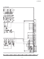
[2] SCHEMATIC DIAGRAM
AV TERMINAL Unit-1/2
,
+
*
)
(
'
&
%
$
#
7–2
LC-42D43U
7–3
LC-42D43U
AV TERMINAL Unit-2/2
,
+
*
)
(
'
&
%
$
#
7–4
LC-42D43U
7–5
LC-42D43U
MAIN Unit-1/20
,
+
*
)
(
'
&
%
$
#
7–6
LC-42D43U
7–7
LC-42D43U
MAIN Unit-2/20
,
+
*
)
(
'
&
%
$
#
7–8
LC-42D43U
7–9
LC-42D43U
MAIN Unit-3/20
,
+
*
)
(
'
&
%
$
#
7 – 10
LC-42D43U
7 – 11
LC-42D43U
MAIN Unit-4/20
,
+
*
)
(
'
&
%
$
#
7 – 12
LC-42D43U
7 – 13
LC-42D43U
MAIN Unit-5/20
,
+
*
)
(
'
&
%
$
#
7 – 14
LC-42D43U
7 – 15
LC-42D43U
MAIN Unit-6/20
,
+
*
)
(
'
&
%
$
#
7 – 16
LC-42D43U
7 – 17
LC-42D43U
MAIN Unit-7/20
,
+
*
)
(
'
&
%
$
#
7 – 18
LC-42D43U
7 – 19
LC-42D43U
MAIN Unit-8/20
,
+
*
)
(
'
&
%
$
#
7 – 20
LC-42D43U
7 – 21
LC-42D43U
MAIN Unit-9/20
,
+
*
)
(
'
&
%
$
#
7 – 22
LC-42D43U
7 – 23
LC-42D43U
MAIN Unit-10/20
,
+
*
)
(
'
&
%
$
#
7 – 24
LC-42D43U
7 – 25
LC-42D43U
MAIN Unit-11/20
,
+
*
)
(
'
&
%
$
#
7 – 26
LC-42D43U
7 – 27
LC-42D43U
MAIN Unit-12/20
,
+
*
)
(
'
&
%
$
#
7 – 28
LC-42D43U
7 – 29
LC-42D43U
MAIN Unit-13/20
,
+
*
)
(
'
&
%
$
#
7 – 30
LC-42D43U
7 – 31
LC-42D43U
MAIN Unit-14/20
,
+
*
)
(
'
&
%
$
#
7 – 32
LC-42D43U
7 – 33
LC-42D43U
MAIN Unit-15/20
,
+
*
)
(
'
&
%
$
#
7 – 34
LC-42D43U
7 – 35
LC-42D43U
MAIN Unit-16/20
,
+
*
)
(
'
&
%
$
#
7 – 36
LC-42D43U
7 – 37
LC-42D43U
MAIN Unit-17/20
,
+
*
)
(
'
&
%
$
#
7 – 38
LC-42D43U
7 – 39
LC-42D43U
MAIN Unit-18/20
,
+
*
)
(
'
&
%
$
#
7 – 40
LC-42D43U
7 – 41
LC-42D43U
MAIN Unit-19/20
,
+
*
)
(
'
&
%
$
#
7 – 42
LC-42D43U
7 – 43
LC-42D43U
MAIN Unit-20/20
,
+
*
)
(
'
&
%
$
#
7 – 44
LC-42D43U
7 – 45
LC-42D43U
— MEMO —
7 – 46
LC-42D43U
PartsGuide
PARTS GUIDE
LCD COLOR TELEVISION
MODEL
LC-42D43U
CONTENTS
[1]
PRINTED WIRING BOARD
ASSEMBLIES
[4]
DUNTKD935FME03 (TERMINAL
Unit)
[2]
LCD PANEL (NOTE: THE PARTS
HERE SHOWN ARE SUPPLIED AS
AN ASSEMBLY BUT NOT
INDEPENDENTLY.)
[5]
CABINET PARTS
[6]
SUPPLIED ACCESSORIES
[7]
PACKING PARTS (NOT
REPLACEMENT ITEM)
[8]
SERVICE JIGS (USE FOR
SERVICING)
[3]
DUNTKD862FM04 (MAIN Unit)
(Only changed parts have been
described.)
Parts marked with " " are important for maintaining the safety of the set. Be sure to replace these
parts with specified ones for maintaining the safety and performance of the set.
This document has been published to be used
for after sales service only.
The contents are subject to change without notice.
LC-42D43U
NO.
PARTS CODE
PRICE NEW PART
RANK MARK DELIVERY
DESCRIPTION
[1] PRINTED WIRING BOARD ASSEMBLIES
N
N
N
DUNTKD862FM04
DUNTKD935FM03
RDENCA226WJQZ
BT
N
N
N
X
MAIN Unit
AV TERMINAL Unit
POWER Unit
[2] LCD PANEL (NOTE: THE PARTS HERE SHOWN ARE SUPPLIED AS AN ASSEMBLY BUT NOT INDEPENDENTLY.)
N
RLCUCA122WJZZ
N
J
42" LCD Panel Module
[3] DUNTKD862FM04 (MAIN Unit) (Only changed parts have been described.)
!
C1118
C1311
C1313
C1403
C1423
C1426
C1433
C1437
C1466
C1467
C2001
D1303
D1311
D8451
D9602
D9606
D9607
D9701
D9702
D9703
FB2604
FB9701
IC1503
IC2003
IC2006
IC3302
IC3304
IC8701
P2601
Q1524
Q1525
Q8452
R1597
R1599
R2069
R2629
R2630
R2631
R8144
R8162
R8163
R8164
R8169
R8170
R8197
R8198
R8199
R9007
R9712
SC1503
TU1101
RC-KZA237WJZZY
RC-KZA237WJZZY
RC-KZA237WJZZY
RC-KZA237WJZZY
RC-KZA237WJZZY
RC-KZA237WJZZY
RC-KZA237WJZZY
RC-KZA237WJZZY
RC-KZA237WJZZY
RC-KZA237WJZZY
RC-KZA237WJZZY
VHDKDS4148/-1Y
RH-EX0264TAZZY
VHDKDS4148/-1Y
RH-EX0256TAZZY
VHDKDS4148/-1Y
RH-EX0256TAZZY
VHDKDS4148/-1Y
VHDKDS4148/-1Y
RH-EX0253TAZZY
RBLN-A206WJZZY
RBLN-0236TAZZY
VHiLVC2G14G-1Y
VHiHC2G66DP-1Y
VHiAHC32PW+-1Y
VHiTAR5SB25-1Y
VHiMST3583M-1Q
VHiTAR5SB33-1Y
QPLGNA493WJZZY
VSRT1N141U/-1Y
VSKTA1535T+-1Y
VSKTA1298Y+-1Y
VRS-CZ1JF103FY
VRS-CZ1JF331JY
VRS-CZ1JF472JY
VRS-CK1JJ000JY
VRS-CK1JJ000JY
VRS-CK1JJ000JY
VRS-CK1JJ470JY
VRS-CK1JJ470JY
VRS-CK1JJ470JY
VRS-CK1JJ470JY
VRS-CK1JJ470JY
VRS-CK1JJ470JY
VRS-CK1JJ470JY
VRS-CK1JJ470JY
VRS-CK1JJ470JY
VRS-CZ1JF472JY
VRS-CZ1JF392JY
QSOCNA004WJZZ
RTUDAA018WJQZ
AB
AB
AB
AB
AB
AB
AB
AB
AB
AB
AB
AA
AB
AA
AB
AA
AB
AA
AA
AC
AA
AA
AD
AD
AD
AD
AZ
AD
AM
AB
AC
AC
AB
AA
AA
AA
AA
AA
AA
AA
AA
AA
AA
AA
AA
AA
AA
AA
AA
AG
BA
N
N
J
J
J
J
J
J
J
J
J
J
J
J
J
J
J
J
J
J
J
J
J
J
J
J
J
J
J
J
J
J
J
J
J
J
J
J
J
J
J
J
J
J
J
J
J
J
J
J
J
J
J
Capacitor 10 16V Ceramic
Capacitor 10 16V Ceramic
Capacitor 10 16V Ceramic
Capacitor 10 16V Ceramic
Capacitor 10 16V Ceramic
Capacitor 10 16V Ceramic
Capacitor 10 16V Ceramic
Capacitor 10 16V Ceramic
Capacitor 10 16V Ceramic
Capacitor 10 16V Ceramic
Capacitor 10 16V Ceramic
Diode KDS4148U-RTK/P
Diode PDZ9.1B,115
Diode KDS4148U-RTK/P
Zener Diode EX0256TA
Diode KDS4148U-RTK/P
Zener Diode EX0256TA
Diode KDS4148U-RTK/P
Diode KDS4148U-RTK/P
Diode PDZ3.3B,115
Balun BLN-A206WJ
Balun BLN-0236TA
IC LVC2G14G-1
IC HC2G66DP-1
IC AHC32PW
IC TAR5SB25
IC S29GL064A90TFIR20H
IC TAR5SB33-1
Plug
Transistor RT1N141U-T111-1
Transistor KTA1535T-RTK/P
Transistor KTA1298Y
Resistor 10k 1/16W Metal Oxide
Resistor 330 1/16W Metal Oxide
Resistor 4.7k 1/16W Metal Oxide
Resistor 0 1/16W Metal Oxide
Resistor 0 1/16W Metal Oxide
Resistor 0 1/16W Metal Oxide
Resistor 47 1/16W Metal Oxide
Resistor 47 1/16W Metal Oxide
Resistor 47 1/16W Metal Oxide
Resistor 47 1/16W Metal Oxide
Resistor 47 1/16W Metal Oxide
Resistor 47 1/16W Metal Oxide
Resistor 47 1/16W Metal Oxide
Resistor 47 1/16W Metal Oxide
Resistor 47 1/16W Metal Oxide
Resistor 4.7k 1/16W Metal Oxide
Resistor 3.9k 1/16W Metal Oxide
Socket
Tuner
J
J
J
J
J
J
J
J
J
J
J
J
J
J
J
J
J
J
J
J
J
J
Capacitor
Capacitor
Capacitor
Capacitor
Capacitor
Capacitor
Capacitor
Capacitor
Capacitor
Capacitor
Capacitor
Capacitor
Capacitor
Capacitor
Capacitor
Capacitor
Capacitor
Capacitor
Capacitor
Capacitor
Capacitor
Capacitor
[4] DUNTKD935FME03 (TERMINAL Unit)
C501
C502
C503
C504
C505
C506
C507
C508
C509
C510
C511
C512
C513
C514
C515
C516
C517
C518
C519
C520
C521
C522
VCKYTV1CB105KY
VCKYTV1CB105KY
RC-KZA510WJPZY
VCKYTV1CB105KY
VCKYTV1CB105KY
RC-KZA510WJPZY
VCKYTV1CB105KY
VCKYTV1CB105KY
RC-KZA510WJPZY
VCKYTV1CB105KY
RC-KZA237WJZZY
VCKYTV1CB105KY
RC-KZA237WJZZY
VCKYTV1CB105KY
VCKYTV1CB105KY
VCKYTV1CB105KY
RC-KZA237WJZZY
VCKYCY1EF104ZY
VCKYCY1HB103KY
VCKYCY1HB103KY
VCKYCY1HB103KY
VCKYTV1CB105KY
AC
AC
AB
AC
AC
AB
AC
AC
AB
AC
AB
AC
AB
AC
AC
AC
AB
AA
AA
AA
AA
AC
2
1 16V Ceramic
1 16V Ceramic
10 16V Ceramic
1 16V Ceramic
1 16V Ceramic
10 16V Ceramic
1 16V Ceramic
1 16V Ceramic
10 16V Ceramic
1 16V Ceramic
10 16V Ceramic
1 16V Ceramic
10 16V Ceramic
1 16V Ceramic
1 16V Ceramic
1 16V Ceramic
10 16V Ceramic
0.1 25V Ceramic
0.01 50V Ceramic
0.01 50V Ceramic
0.01 50V Ceramic
1 16V Ceramic
LC-42D43U
NO.
PARTS CODE
PRICE NEW PART
RANK MARK DELIVERY
DESCRIPTION
[4] DUNTKD935FME03 (TERMINAL Unit)
C523
C524
C525
C526
C527
C528
C529
C530
C532
C536
C537
C538
C540
C541
C543
C544
C545
C546
C547
C551
C552
C553
C554
C555
C556
C557
C564
C567
C575
C2701
C2702
C2703
C2704
C2705
C2706
C2707
C2708
C2709
C2710
C2711
C2712
C2713
C2714
C2715
C2716
C2717
C2718
C2720
C2725
C2726
C2727
C2728
C2729
C2730
C2731
C2732
C2733
C2734
C2737
C2738
C2739
C2740
C2741
C2742
C2744
C2745
C2746
C2747
D501
D502
D503
D504
D505
D506
D507
D508
D509
D510
D511
D512
D513
D514
D515
D516
D517
VCKYCY1EF104ZY
VCAAPF1CJ396MY
VCKYCY1EF104ZY
VCKYCY1EF104ZY
VCKYCY1EF104ZY
VCERML1CN226MY
VCKYCY1EF104ZY
VCKYCY1EF104ZY
VCKYCY1EF104ZY
VCKYCH1CB104KY
VCKYCH1CB104KY
VCKYCH1CB104KY
RC-KZA510WJPZY
VCKYCH1CB104KY
VCKYCH1CB104KY
VCKYCY1EF104ZY
VCKYCY1EF104ZY
VCKYCY1EF104ZY
VCERMZ1CN107MY
VCKYCY1EF104ZY
VCKYCY1EF104ZY
VCKYCY1EF104ZY
VCAAPF1CJ396MY
RC-KZA154WJZZY
RC-KZA154WJZZY
RC-KZA104WJZZY
VCKYCH1CB104KY
VCKYCY1EF104ZY
VCAAPF1CJ396MY
RC-KZA104WJZZY
RC-KZA104WJZZY
RC-KZA104WJZZY
RC-KZA104WJZZY
RC-KZA104WJZZY
RC-KZA104WJZZY
VCKYCY1HF224ZY
VCKYCY1EF104ZY
VCKYCY1HF224ZY
VCKYCY1HF224ZY
VCKYCY1HF224ZY
RC-KZA104WJZZY
RC-KZA104WJZZY
VCERMZ1EN227MY
RC-KZA104WJZZY
RC-KZA104WJZZY
VCKYCY1HB104KY
VCKYCY1HB104KY
VCERMZ1EN227MY
VCKYCY1HB104KY
VCKYCY1HB104KY
VCKYCY1HB104KY
VCKYCY1HB104KY
VCKYTV1EB474KY
VCKYTV1EB474KY
RC-KZA516WJQZY
RC-KZA516WJQZY
VCCCCY1HH151JY
VCCCCY1HH151JY
VCKYCY1HB104KY
VCKYCY1HB104KY
VCKYCY1HB104KY
VCKYCY1HB104KY
VCCCCY1HH151JY
VCCCCY1HH151JY
VCAAPC1EJ106MY
VCKYCY1HB103KY
RC-KZA110WJZZY
RC-KZA110WJZZY
RH-EX1400CEZZY
RH-EX1400CEZZY
RH-EX1400CEZZY
RH-EX1400CEZZY
RH-EX1400CEZZY
RH-EX1400CEZZY
RH-EX1400CEZZY
RH-EX1400CEZZY
RH-EX1400CEZZY
RH-EX1400CEZZY
RH-EX1400CEZZY
VHDDAN217U+-1Y
VHDDAN217U+-1Y
VHDDAN217U+-1Y
VHDDAN217U+-1Y
VHDDAN217U+-1Y
VHDDAN217U+-1Y
AA
AF
AA
AA
AA
AC
AA
AA
AA
AB
AB
AB
AB
AB
AB
AA
AA
AA
AD
AA
AA
AA
AF
AB
AB
AA
AB
AA
AF
AA
AA
AA
AA
AA
AA
AA
AA
AA
AA
AA
AA
AA
AE
AA
AA
AA
AA
AE
AA
AA
AA
AA
AC
AC
AC
AC
AA
AA
AA
AA
AA
AA
AA
AA
AF
AA
AD
AD
AB
AB
AB
AB
AB
AB
AB
AB
AB
AB
AB
AB
AB
AB
AB
AB
AB
N
N
J
J
J
J
J
J
J
J
J
J
J
J
J
J
J
J
J
J
J
J
J
J
J
J
J
J
J
J
J
J
J
J
J
J
J
J
J
J
J
J
J
J
J
J
J
J
J
J
J
J
J
J
J
J
J
J
J
J
J
J
J
J
J
J
J
J
J
J
J
J
J
J
J
J
J
J
J
J
J
J
J
J
J
J
J
Capacitor 0.1 25V Ceramic
Capacitor 39 16V Electrolytic
Capacitor 0.1 25V Ceramic
Capacitor 0.1 25V Ceramic
Capacitor 0.1 25V Ceramic
Capacitor 22 16V Electrolytic
Capacitor 0.1 25V Ceramic
Capacitor 0.1 25V Ceramic
Capacitor 0.1 25V Ceramic
Capacitor 0.1 16V Ceramic
Capacitor 0.1 16V Ceramic
Capacitor 0.1 16V Ceramic
Capacitor 10 16V Ceramic
Capacitor 0.1 16V Ceramic
Capacitor 0.1 16V Ceramic
Capacitor 0.1 25V Ceramic
Capacitor 0.1 25V Ceramic
Capacitor 0.1 25V Ceramic
Capacitor 100 16V Electrolytic
Capacitor 0.1 25V Ceramic
Capacitor 0.1 25V Ceramic
Capacitor 0.1 25V Ceramic
Capacitor 39 16V Electrolytic
Capacitor 4.7 16V Ceramic
Capacitor 4.7 16V Ceramic
Capacitor 1 25V Ceramic
Capacitor 0.1 16V Ceramic
Capacitor 0.1 25V Ceramic
Capacitor 39 16V Electrolytic
Capacitor 1 25V Ceramic
Capacitor 1 25V Ceramic
Capacitor 1 25V Ceramic
Capacitor 1 25V Ceramic
Capacitor 1 25V Ceramic
Capacitor 1 25V Ceramic
Capacitor 0.22 50V Ceramic
Capacitor 0.1 25V Ceramic
Capacitor 0.22 50V Ceramic
Capacitor 0.22 50V Ceramic
Capacitor 0.22 50V Ceramic
Capacitor 1 25V Ceramic
Capacitor 1 25V Ceramic
Capacitor 220 25V Electrolytic
Capacitor 1 25V Ceramic
Capacitor 1 25V Ceramic
Capacitor 0.1 50V Ceramic
Capacitor 0.1 50V Ceramic
Capacitor 220 25V Electrolytic
Capacitor 0.1 50V Ceramic
Capacitor 0.1 50V Ceramic
Capacitor 0.1 50V Ceramic
Capacitor 0.1 50V Ceramic
Capacitor 0.47 25V Ceramic
Capacitor 0.47 25V Ceramic
Capacitor 0.68 35V Ceramic
Capacitor 0.68 35V Ceramic
Capacitor 150p 50V Ceramic
Capacitor 150p 50V Ceramic
Capacitor 0.1 50V Ceramic
Capacitor 0.1 50V Ceramic
Capacitor 0.1 50V Ceramic
Capacitor 0.1 50V Ceramic
Capacitor 150p 50V Ceramic
Capacitor 150p 50V Ceramic
Capacitor 10 25V Electrolytic
Capacitor 0.01 50V Ceramic
Capacitor
Capacitor
Zener Diode UDZSTE-1710B, 10V
Zener Diode UDZSTE-1710B, 10V
Zener Diode UDZSTE-1710B, 10V
Zener Diode UDZSTE-1710B, 10V
Zener Diode UDZSTE-1710B, 10V
Zener Diode UDZSTE-1710B, 10V
Zener Diode UDZSTE-1710B, 10V
Zener Diode UDZSTE-1710B, 10V
Zener Diode UDZSTE-1710B, 10V
Zener Diode UDZSTE-1710B, 10V
Zener Diode UDZSTE-1710B, 10V
Diode DAN217UT106
Diode DAN217UT106
Diode DAN217UT106
Diode DAN217UT106
Diode DAN217UT106
Diode DAN217UT106
3
LC-42D43U
NO.
PARTS CODE
PRICE NEW PART
RANK MARK DELIVERY
DESCRIPTION
[4] DUNTKD935FME03 (TERMINAL Unit)
D518
D519
D2701
FB501
FB502
FB503
FB504
FB505
FB506
FB507
FB508
FB509
FB510
FB511
FB512
FB513
FB514
FB515
FB516
FB517
FB518
FB519
FB520
FB531
FB532
FB533
FB534
FB2709
FB2710
FB2711
FB2712
IC501
IC2701
J501
J502
J503
L2701
L2702
L2703
L2704
LUG501
LUG502
LUG2701
LUG2702
P502
P2703
P2704
Q501
Q502
Q503
Q504
Q505
Q506
Q507
Q508
Q509
R501
R502
R503
R504
R505
R506
R507
R508
R509
R510
R511
R512
R513
R514
R515
R516
R517
R518
R519
R520
R521
R522
R523
R524
R525
R526
R527
R528
R529
RH-EX1400CEZZY
RH-EX1400CEZZY
VHDKDS226//-1Y
RBLN-A204WJZZY
RBLN-A204WJZZY
RBLN-A204WJZZY
RBLN-0065TAZZY
RBLN-0065TAZZY
RBLN-A204WJZZY
RBLN-0065TAZZY
RBLN-0065TAZZY
RBLN-A204WJZZY
RBLN-A204WJZZY
RBLN-A204WJZZY
RBLN-0065TAZZY
RBLN-0065TAZZY
RBLN-A204WJZZY
RBLN-0065TAZZY
RBLN-0065TAZZY
RBLN-A204WJZZY
RBLN-A204WJZZY
RBLN-A204WJZZY
RBLN-0039TAZZY
RBLN-A206WJZZY
RBLN-A206WJZZY
RBLN-A206WJZZY
RBLN-A206WJZZY
RBLN-0064TAZZY
RBLN-0064TAZZY
RBLN-0064TAZZY
RBLN-0064TAZZY
VHiMM3151XQ-1Q
VHiTPA3100D-1Y
QTANJA092WJZZ
QTANJA093WJZZ
QSOCDA020WJZZ
RCiLPA479WJZZY
RCiLPA479WJZZY
RCiLPA479WJZZY
RCiLPA479WJZZY
QLUGHA006WJZZY
QLUGHA006WJZZY
QLUGHA006WJZZY
QLUGHA006WJZZY
QPLGNA347WJZZY
QPLGNA173WJZZY
QCNCMA250WJZZ
VS2SA1530AR-1Y
VS2SC3928AR-1Y
VS2SA1530AR-1Y
VS2SC3928AR-1Y
VS2SA1530AR-1Y
VS2SC3928AR-1Y
VSDTC614TK+-1Y
VSDTC614TK+-1Y
VS2SA1530AR-1Y
VRS-TQ2BD750JY
VRS-CY1JF102JY
VRS-TQ2BD750JY
VRS-CY1JF102JY
VRS-TQ2BD750JY
VRS-CY1JF102JY
VRS-CY1JF221JY
VRS-CY1JF104JY
VRS-CY1JF221JY
VRS-CY1JF104JY
VRS-TQ2BD750JY
VRS-CY1JF221JY
VRS-CY1JF104JY
VRS-TQ2BD750JY
VRS-CY1JF221JY
VRS-CY1JF104JY
VRS-TQ2BD750JY
VRS-CY1JF102JY
VRS-TQ2BD750JY
VRS-CY1JF102JY
VRS-CY1JF221JY
VRS-CY1JF104JY
VRS-CY1JF221JY
VRS-CY1JF104JY
VRS-TQ2BD750JY
VRS-CY1JF221JY
VRS-CY1JF104JY
VRS-CY1JF104JY
VRS-CY1JF221JY
AB
AB
AB
AA
AA
AA
AA
AA
AA
AA
AA
AA
AA
AA
AA
AA
AA
AA
AA
AA
AA
AA
AB
AA
AA
AA
AA
AB
AB
AB
AB
AT
AQ
AG
AG
AC
AE
AE
AE
AE
AC
AC
AC
AC
AD
AD
AE
AB
AB
AB
AB
AB
AB
AB
AB
AB
AA
AA
AA
AA
AA
AA
AA
AA
AA
AA
AA
AA
AA
AA
AA
AA
AA
AA
AA
AA
AA
AA
AA
AA
AA
AA
AA
AA
AA
N
J
J
J
J
J
J
J
J
J
J
J
J
J
J
J
J
J
J
J
J
J
J
J
J
J
J
J
J
J
J
J
J
J
J
J
J
J
J
J
J
J
J
J
J
J
J
J
J
J
J
J
J
J
J
J
J
J
J
J
J
J
J
J
J
J
J
J
J
J
J
J
J
J
J
J
J
J
J
J
J
J
J
J
J
J
Zener Diode UDZSTE-1710B, 10V
Zener Diode UDZSTE-1710B, 10V
Diode KDS226-RTK/P
Balun BLN-A204WJ
Balun BLN-A204WJ
Balun BLN-A204WJ
Balun BLN-0065TA
Balun BLN-0065TA
Balun BLN-A204WJ
Balun BLN-0065TA
Balun BLN-0065TA
Balun BLN-A204WJ
Balun BLN-A204WJ
Balun BLN-A204WJ
Balun BLN-0065TA
Balun BLN-0065TA
Balun BLN-A204WJ
Balun BLN-0065TA
Balun BLN-0065TA
Balun BLN-A204WJ
Balun BLN-A204WJ
Balun BLN-A204WJ
Balun BLN-0039TA
Balun BLN-A206WJ
Balun BLN-A206WJ
Balun BLN-A206WJ
Balun BLN-A206WJ
Balun BLN-0064TA
Balun BLN-0064TA
Balun BLN-0064TA
Balun BLN-0064TA
IC MM3151XQ
IC TPA3100D2PHPR
Terminal INPUT1
Terminal INPUT2
Socket
Coil
Coil
Coil
Coil
Lug
Lug
Lug
Lug
Plug 13pin
Plug 4pin (SP)
Connector 23pin
Transistor 2SA1530A-T112-1R
Transistor 2SC3928A-T112-1R
Transistor 2SA1530A-T112-1R
Transistor 2SC3928A-T112-1R
Transistor 2SA1530A-T112-1R
Transistor 2SC3928A-T112-1R
Transistor DTC614TKT146
Transistor DTC614TKT146
Transistor 2SA1530A-T112-1R
Resistor 75 1/8W Metal Oxide
Resistor 1k 1/16W Metal Oxide
Resistor 75 1/8W Metal Oxide
Resistor 1k 1/16W Metal Oxide
Resistor 75 1/8W Metal Oxide
Resistor 1k 1/16W Metal Oxide
Resistor 220 1/16W Metal Oxide
Resistor 100k 1/16W Metal Oxide
Resistor 220 1/16W Metal Oxide
Resistor 100k 1/16W Metal Oxide
Resistor 75 1/8W Metal Oxide
Resistor 220 1/16W Metal Oxide
Resistor 100k 1/16W Metal Oxide
Resistor 75 1/8W Metal Oxide
Resistor 220 1/16W Metal Oxide
Resistor 100k 1/16W Metal Oxide
Resistor 75 1/8W Metal Oxide
Resistor 1k 1/16W Metal Oxide
Resistor 75 1/8W Metal Oxide
Resistor 1k 1/16W Metal Oxide
Resistor 220 1/16W Metal Oxide
Resistor 100k 1/16W Metal Oxide
Resistor 220 1/16W Metal Oxide
Resistor 100k 1/16W Metal Oxide
Resistor 75 1/8W Metal Oxide
Resistor 220 1/16W Metal Oxide
Resistor 100k 1/16W Metal Oxide
Resistor 100k 1/16W Metal Oxide
Resistor 220 1/16W Metal Oxide
4
LC-42D43U
NO.
PARTS CODE
PRICE NEW PART
RANK MARK DELIVERY
DESCRIPTION
[4] DUNTKD935FME03 (TERMINAL Unit)
R530
R531
R532
R533
R534
R535
R536
R537
R538
R539
R540
R541
R542
R548
R549
R550
R554
R555
R556
R557
R558
R559
R561
R562
R563
R564
R565
R566
R567
R568
R570
R571
R572
R573
R574
R576
R577
R578
R579
R580
R582
R583
R584
R585
R586
R587
R588
R589
R590
R591
R592
R593
R594
R604
R611
R612
R613
R614
R615
R616
R617
R618
R619
R2701
R2702
R2705
R2706
R2713
R2714
R2722
R2723
R2724
SC501
SC502
N
VRS-TQ2BD750JY
VRS-CY1JF102JY
VRS-TQ2BD750JY
VRS-CY1JF274JY
VRS-CY1JF103JY
VRS-TQ2BD750JY
VRS-CY1JF101JY
VRS-CY1JF101JY
VRS-CY1JF101JY
VRS-CY1JF101JY
VRS-CY1JF101JY
VRS-CY1JF101JY
VRS-CY1JF000JY
VRS-CY1JF220JY
VRS-CY1JF220JY
VRS-CY1JF220JY
VRS-CY1JF220JY
VRS-CY1JF220JY
VRS-CY1JF220JY
VRS-CY1JF101JY
VRS-CY1JF101JY
VRS-CJ1JF470JY
VRS-CY1JF223JY
VRS-CY1JF101JY
VRS-CY1JF223JY
VRS-CY1JF101JY
VRS-CY1JF101JY
VRS-CY1JF223JY
VRS-CY1JF101JY
VRS-CY1JF223JY
VRS-CY1JF331JY
VRS-CY1JF331JY
VRS-CY1JF000JY
VRS-TV1JD102JY
VRS-CY1JF680JY
VRS-CY1JF331JY
VRS-CY1JF331JY
VRS-CY1JF000JY
VRS-TV1JD102JY
VRS-CY1JF680JY
VRS-CY1JF331JY
VRS-CY1JF331JY
VRS-CY1JF000JY
VRS-TV1JD102JY
VRS-CY1JF680JY
VRS-CY1JF561JY
VRS-CY1JF561JY
VRS-CY1JF564JY
VRS-CY1JF564JY
VRS-CJ1JF102JY
VRS-CY1JF473JY
VRS-CY1JF473JY
VRS-CY1JF332JY
VRS-CY1JF000JY
VRS-CY1JF000JY
VRS-CY1JF000JY
VRS-CY1JF000JY
VRS-CY1JF000JY
VRS-CY1JF000JY
VRS-CY1JF000JY
VRS-CY1JF000JY
VRS-CY1JF000JY
VRS-CY1JF000JY
VRS-CY1JF104JY
VRS-CY1JF104JY
VRS-CY1JF104JY
VRS-CY1JF104JY
VRS-TQ2EF220JY
VRS-TQ2EF220JY
VRS-TQ2EF220JY
VRS-TQ2EF220JY
VRS-CY1JF220JY
QCNCMA250WJZZ
QCNCMA250WJZZ
QCNW-F018WJQZ
AA
AA
AA
AA
AA
AA
AA
AA
AA
AA
AA
AA
AA
AA
AA
AA
AA
AA
AA
AA
AA
AA
AA
AA
AA
AA
AA
AA
AA
AA
AA
AA
AA
AA
AA
AA
AA
AA
AA
AA
AA
AA
AA
AA
AA
AA
AA
AA
AA
AA
AA
AA
AA
AA
AA
AA
AA
AA
AA
AA
AA
AA
AA
AA
AA
AA
AA
AA
AA
AA
AA
AA
AE
AE
AL
J
J
J
J
J
J
J
J
J
J
J
J
J
J
J
J
J
J
J
J
J
J
J
J
J
J
J
J
J
J
J
J
J
J
J
J
J
J
J
J
J
J
J
J
J
J
J
J
J
J
J
J
J
J
J
J
J
J
J
J
J
J
J
J
J
J
J
J
J
J
J
J
J
J
X
Resistor 75 1/8W Metal Oxide
Resistor 1k 1/16W Metal Oxide
Resistor 75 1/8W Metal Oxide
Resistor 270k 1/16W Metal Oxide
Resistor 10k 1/16W Metal Oxide
Resistor 75 1/8W Metal Oxide
Resistor 100 1/16W Metal Oxide
Resistor 100 1/16W Metal Oxide
Resistor 100 1/16W Metal Oxide
Resistor 100 1/16W Metal Oxide
Resistor 100 1/16W Metal Oxide
Resistor 100 1/16W Metal Oxide
Resistor 0 1/16W Metal Oxide
Resistor 22 1/16W Metal Oxide
Resistor 22 1/16W Metal Oxide
Resistor 22 1/16W Metal Oxide
Resistor 22 1/16W Metal Oxide
Resistor 22 1/16W Metal Oxide
Resistor 22 1/16W Metal Oxide
Resistor 100 1/16W Metal Oxide
Resistor 100 1/16W Metal Oxide
Resistor 47 1/16W Metal Oxide
Resistor 22k 1/16W Metal Oxide
Resistor 100 1/16W Metal Oxide
Resistor 22k 1/16W Metal Oxide
Resistor 100 1/16W Metal Oxide
Resistor 100 1/16W Metal Oxide
Resistor 22k 1/16W Metal Oxide
Resistor 100 1/16W Metal Oxide
Resistor 22k 1/16W Metal Oxide
Resistor 330 1/16W Metal Oxide
Resistor 330 1/16W Metal Oxide
Resistor 0 1/16W Metal Oxide
Resistor 1k 1/10W Metal Oxide
Resistor 68 1/16W Metal Oxide
Resistor 330 1/16W Metal Oxide
Resistor 330 1/16W Metal Oxide
Resistor 0 1/16W Metal Oxide
Resistor 1k 1/10W Metal Oxide
Resistor 68 1/16W Metal Oxide
Resistor 330 1/16W Metal Oxide
Resistor 330 1/16W Metal Oxide
Resistor 0 1/16W Metal Oxide
Resistor 1k 1/10W Metal Oxide
Resistor 68 1/16W Metal Oxide
Resistor 560 1/16W Metal Oxide
Resistor 560 1/16W Metal Oxide
Resistor 560k 1/16W Metal Oxide
Resistor 560k 1/16W Metal Oxide
Resistor 1k 1/16W Metal Oxide
Resistor 47k 1/16W Metal Oxide
Resistor 47k 1/16W Metal Oxide
Resistor 3.3k 1/16W Metal Oxide
Resistor 0 1/16W Metal Oxide
Resistor 0 1/16W Metal Oxide
Resistor 0 1/16W Metal Oxide
Resistor 0 1/16W Metal Oxide
Resistor 0 1/16W Metal Oxide
Resistor 0 1/16W Metal Oxide
Resistor 0 1/16W Metal Oxide
Resistor 0 1/16W Metal Oxide
Resistor 0 1/16W Metal Oxide
Resistor 0 1/16W Metal Oxide
Resistor 100k 1/16W Metal Oxide
Resistor 100k 1/16W Metal Oxide
Resistor 100k 1/16W Metal Oxide
Resistor 100k 1/16W Metal Oxide
Resistor 22 1/4W Metal Oxide
Resistor 22 1/4W Metal Oxide
Resistor 22 1/4W Metal Oxide
Resistor 22 1/4W Metal Oxide
Resistor 22 1/16W Metal Oxide
Connector 23pin
Connector 23pin
Connecting Cord (RA)
5
LC-42D43U
[5] CABINET PARTS
3
3-1
7
41
5
3-2
25
42
35
28
54
48
43
1
28
1-6
1-6
1-1
1-7
1-4
48
1-6
1-6
1-5
1-6
1-6
54
1-9
1-3
55
2
52
15
4-4
1-7
1-7
1-7
6
1-7
1-7
1-8
2-1
1-2
1-7
52
49
23
46
38
23
49
50
10
49
47
49 50
44
49
16-3
55
49
49
49
16-2
16-1
17-2
55
50
36
19
34
49
21
20
31
12
50
17
50
50
40
49
29
24-3
49 35
32
18
49
39
22
26
9
4-2
51
30
11
14 53
13
4
4-1
4-3
55
55
55
6
49
49 49
24-2
17-3
55
8
24-1
27
17-1
33
37
18
49
55
45
24-4 24-4
24-3 24-3
24
16
2-2
49
55
LC-42D43U
NO.
PARTS CODE
PRICE NEW PART
RANK MARK DELIVERY
DESCRIPTION
[5] CABINET PARTS
1
1-1
1-2
1-3
1-4
1-5
1-6
1-7
1-8
1-9
2
2-1
2-2
3
3-1
3-2
4
4-1
4-2
4-3
4-4
5
6
7
8
9
10
11
12
13
14
15
16
16-1
16-2
16-3
17
17-1
17-2
17-3
18
19
20
21
22
23
24
24-1
24-2
24-3
24-4
25
26
27
28
29
30
31
32
33
34
35
36
37
38
39
40
41
42
43
44
45
46
47
48
49
50
51
52
53
54
55
CCABAB803WJ01
GCOVAB821WJSA
GCOVAC312WJSA
HDECSA020WJSA
HPNLSA139WJSA
Not available
PSPAZB226WJZZ
TLABZA635WJZZ
XJPSN30P08XS0
CCABBB064WJ01
LHLDWA131WJKZ
CCOVAB914WJ01
Not available
CDAi-A327WJ02
CDAi-A327WJ01
CDAi-A328WJ01
LX-BZA146WJF7
LX-BZA147WJF8
RLCUCA122WJZZ
DUNTKD909FM02
DUNTKD910FM02
DUNTKD862FM04
DUNTKD935FM03
RDENCA226WJQZ
GCOVAA678WJKA
GCOVAB912WJKA
HiNDPB715WJSA
HiNDPC354WJSA
HiNDPC419WJSA
CANGKA839WJ01
Not available
LHLDWA120WJKZ
Not available
CANGKA840WJ02
Not available
LHLDWA120WJKZ
Not available
LANGKA841WJFW
LANGKA879WJFW
LANGKA881WJFW
LANGKA882WJFW
LANGKB264WJFW
LANGTA401WJFW
CCHSMA341WJ02
Not available
LHLDWA102WJKZ
LHLDWA120WJKZ
LHLDWA123WJKZ
LHLDWA141WJZZ
LHLDWA150WJKZ
LHLDWA163WJKZ
LX-HZA003WJFN
LX-NZ3047GEZZ
NSFTZ0134CEFW
PCLiCA004WJKZ
PMLT-A390WJZZ
PRDARA414WJFW
PSLDMA910WJN1
PSLDMB066WJZZ
PSPAZA635WJKZ
PSPAZA917WJKZ
PZETKA272WJZZ
QCNCWA496WJZZ
QCNW-E249WJPZ
QCNW-E703WJPZ
QCNW-E897WJQZ
QCNW-F017WJQZ
QCNW-F019WJQZ
QCNW-F733WJQZ
QCNW-F742WJQZ
RCORFA020WJZZ
RSP-ZA278WJZZ
XBBS740P06000
XBPS730P06WS0
XBPS830P06000
XBPS930P08JS0
XEBS930P08000
XEBS930P10000
XEBS940P20000
BU
-
N
N
AQ
AW
N
N
N
N
AD
AC
AA
BL
AE
AS
BN
N
N
N
N
N
N
AC
AE
N
N
N
BT
AE
AQ
AC
AH
AH
AY
AB
AZ
AB
AM
AT
AM
AM
AM
AT
BA
AB
AB
AB
AD
AC
AC
AC
AA
AD
AC
AH
AK
AW
AG
AC
AH
AP
AK
AH
AX
AF
AH
AN
AG
AS
AN
AA
AA
AA
AB
AA
AA
AB
N
N
N
N
N
N
N
N
N
N
N
N
N
N
N
N
N
N
N
N
N
X
X
X
X
J
J
J
X
J
X
X
J
J
J
X
J
X
X
X
X
X
J
X
J
X
J
J
J
X
J
X
J
J
J
J
J
J
J
J
J
J
X
X
J
X
J
J
X
J
J
X
J
X
J
X
X
J
J
J
J
J
J
J
J
J
Front Cabinet Ass'y
Front Cabinet
LED Cover
Front Cover
Shaine Trim
SP Net
Mask Himelon, x6
Tape, x7
E-Star Label
Screw, x3
Rear Cabinet Ass'y
Rear Cabinet
Wire Holder
Top Cover Ass'y
Top Cover
Cntrol Button
Stand Ass'y
Stand Base Ass'y
Stand Support Ass'y
Screw, x4
Screw, x4
42" LCD Panel Module
R/C, LED Unit
KEY Unit
MAIN Unit
AV TERMINAL Unit
POWER Unit
SD Card Cover
Stand Assist Cover
Terminal Label
Jack Indicator
Model Label
Rug Angle Top Ass'y
Rug Angle Top
Wire Holder
Rug Spacer, x2
Rug Anglke Bottom Ass'y
Rug Anglke Bottom
Wire Holder, x8
Rug Spacer, x2
Tray Fix Angle, x2
Stand Fix Angle
Stand Assist Angle
Chassis Fix Angle
Terminal Angle
Center Angle, x2
Chassis Tray Ass'y
Chassis Tray
Wire Holder, x1
Wire Holder, x4
Wire Holder, x2
Wire Holder
Edge Saddle WH
Wire Holder, x4
Screw, x2 (for Speaker)
Hexagonal Nut
Hexagonal Shaft, x2
Rivet, x3
Absorber
Heat Sink
Main Shield
Spacer, x4
Spacer
Cool Sheet
Insulation Sheet
Connector (F-RCA)
Connecting Cord (TUNER)
Connecting Cord (LV)
Connecting Cord (KM)
Connecting Cord (SP)
Connecting Cord (PE/PD)
Connecting Cord (Model Detect)
Connecting Cord (LA)
Core
Speaker Box, x2
Screw, x33 (for Angle)
Screw, x25 (for PWB16/Angle9)
Screw, x2 (for HDMI)
Screw, x5 (for Rear Cabinet)
Screw, x3 (for JACK)
Screw, x1
Screw, x22 (for Rear Cabinet)
7
LC-42D43U
[6] SUPPLIED ACCESSORIES
:
: :
:
:
:
:
:
:
8
LC-42D43U
NO.
PARTS CODE
PRICE NEW PART
RANK MARK DELIVERY
DESCRIPTION
[6] SUPPLIED ACCESSORIES
!
X1
X2
X3
X4
X5
X6
X7
X8
X9
LHLDWA012WJKZ
LHLDWA083WJ00
LHLDWA131WJKZ
QACCDA039WJPZ
RRMCGA535WJSA
TCADEA208WJZZ
TiNS-D068WJZZ
TGAN-A845WJZZ
CDAi-A327WJ02
AC
AD
AE
AQ
AZ
AD
AP
AP
BN
N
J
J
J
J
J
X
X
X
X
Cable Clamp
Cable Band
Cable Clamp
AC Cord
Remote Control Unit
Questionnaire Card
Operation Manual
Extend Warranty Card
Stand Ass'y
9
LC-42D43U
[7] PACKING PARTS (NOT REPLACEMENT ITEM)
S6
S7
S4
S4
S1
S3
S5
S4
S4
S2
10
LC-42D43U
NO.
PARTS CODE
PRICE NEW PART
RANK MARK DELIVERY
DESCRIPTION
[7] PACKING PARTS (NOT REPLACEMENT ITEM)
S1
S2
S3
S4
S5
S6
S7
SPAKCD512WJZZ
SPAKCD085WJZZ
SPAKPA774WJZZ
SPAKXB531WJZZ
TLABKA009WJZZ
SSAKA0101GJZZ
SSAKAA032WJZZ
AB
N
N
J
Packing Case
Bottom Case
Wrapping Paper
Buffer Material
No. Label
Polyethylene Bag
Polyethylene Bag
J
J
J
J
J
J
L=1000mm, x2, POWER to INV.1/2(LA1/LA2) L=1250mm,
4pis-2pins/2pins, L=1000mm, Terminal Unit to Speak
13pins L=1000mm, Terminal unit to R/C LED Unit (R
12pins L=1000mm, Main Unit to Power Unit (PE)
6pins L=1000mm, Main Unit to Power Unit (PD)
30pins L=1000mm, Main Unit to Controller Unit (LV)
[8] SERVICE JIGS (USE FOR SERVICING)
N
N
N
N
N
N
QCNW-G383WJQZ
QCNW-F138WJQZ
QCNW-F139WJQZ
QCNW-D483WJQZ
QCNW-E068WJQZ
QCNW-E673WJPZ
AW
AP
AX
AX
AS
BE
11
LC42D43U
2007 BY SHARP CORPORATION
COPYRIGHT © 2006
ALL RIGHTS RESERVED.
No Part of this publication may be reproduced,
stored in a retrieval system, or transmitted in
any from or by any means, electronic, mechanical,
photocopying , recording, or otherwise, without
prior written permission of the publisher.
Jun. 2007 Printed in Japan
TQ
-S SH. DS
SHARP CORPORATION
AV Systems Group
CS Promotion Center
Yaita,Tochigi 329-2193, Japan