1
CY7C68013A, CY7C68014A
CY7C68015A, CY7C68016A
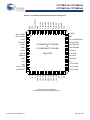
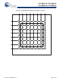
3. Pin Assignments
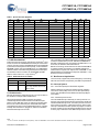
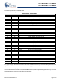
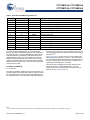
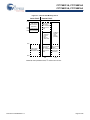
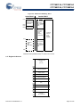
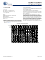
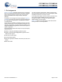
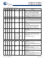
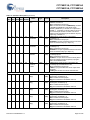
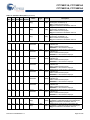
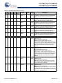
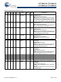
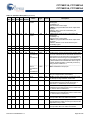
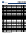
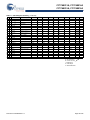
Figure 3-1 on page 16 identifies all signals for the five package
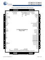
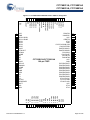
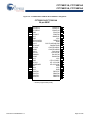
types. The following pages illustrate the individual pin diagrams,
plus a combination diagram showing which of the full set of
signals are available in the 128-pin, 100-pin, and 56-pin
packages.
The signals on the left edge of the 56-pin package in Figure 3-1
on page 16 are common to all versions in the FX2LP family with
the noted differences between the CY7C68013A/14A and the
CY7C68015A/16A.
The 128-pin package adds the 8051 address and data buses
plus control signals. Note that two of the required signals, RD#
and WR#, are present in the 100-pin version.
In the 100-pin and 128-pin versions, an 8051 control bit can be
set to pulse the RD# and WR# pins when the 8051 reads
from/writes to PORTC. This feature is enabled by setting
PORTCSTB bit in CPUCS register.
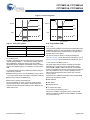
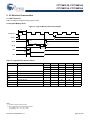
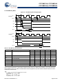
Section 9.5 displays the timing diagram of the read and write
strobing function on accessing PORTC.
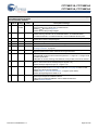
Three modes are available in all package versions: Port, GPIF
master, and Slave FIFO. These modes define the signals on the
right edge of the diagram. The 8051 selects the interface mode
using the IFCONFIG[1:0] register bits. Port mode is the power on
default configuration.
The 100-pin package adds functionality to the 56-pin package by
adding these pins:
■
PORTC or alternate GPIFADR[7:0] address signals
■
PORTE or alternate GPIFADR[8] address signal and seven
additional 8051 signals
■
Three GPIF Control signals
■
Four GPIF Ready signals
■
Nine 8051 signals (two USARTs, three timer inputs, INT4,and
INT5#)
■
BKPT, RD#, WR#.
Document #: 38-08032 Rev. *V
Page 15 of 66