1
SBC8140
Single Board Computer
User Manual
Version 1.1
22nd Jan 2014
Copyright Statement:
SBC8140 and its related intellectual property are owned by
Shenzhen Embest Technology Co., Ltd.
Shenzhen Embest Technology has the copyright of this document
and reserves all rights. Any part of the document should not be
modified, distributed or duplicated in any approach and form
without prior written permission issued by Embest Technology Co.,
Ltd.
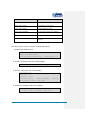
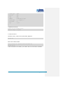
Revision History:
Version
Date
Description
1.0
20/03/2013
Original Version
1.1
22/01/2014
Localisation
Table of Contents
1 Product Overview ............................................................ 1
1.1 Introduction ................................................................. 1
1.2 Kit Contents ................................................................. 1
1.3 Product Features ........................................................... 2
1.3.1 Mini8510 Core Board ............................................................... 2
1.3.2 Expansion Board ..................................................................... 4
1.4 Interfaces on the SBC8140 ............................................. 6
1.5 System Block Diagram ................................................... 7
1.6 Hardware Dimensions .................................................... 8
1.6.1 MINI8510 Core Board .............................................................. 8
1.6.2 Expansion Board ..................................................................... 9
1.7 Modules Supported by SBC8140 ..................................... 10
2 Introduction to Hardware .............................................. 11
2.1 CPU Introduction .......................................................... 11
2.1.1 Clock ................................................................................... 11
2.1.2 Reset ................................................................................... 11
2.1.3 General Interfaces ................................................................. 11
2.1.4 Display Subsystem ................................................................. 12
2.1.5 3D Graphics Acceleration System ............................................. 12
2.2 Peripheral ICs around CPU ............................................. 13
2.2.1 TPS65930 Power Management IC ............................................. 13
2.2.2 H9DA4GH2GJAMCR Memory .................................................... 14
2.2.3 DM9000 Ethernet Controller ..................................................... 14
2.2.4 FE1.1 USB Hub ...................................................................... 14
2.2.5 TFP410 Flat Panel Display IC .................................................... 14
2.2.6 MAX3232 Transceiver ............................................................. 15
2.3 Hardware Interfaces and LEDs on Mini8510 ...................... 16
2.3.1 CN1 90pin DIP Interface (right row) .......................................... 16
2.3.2 CN2 90pin DIP Interface (left row) ............................................ 21
2.3.3 CN3 JTAG Interface ................................................................ 25
2.3.4 CN4 Camera Interface ............................................................ 25
2.3.5 LED Indicators ....................................................................... 27
2.4 Interfaces on Expansion Board ....................................... 27
2.4.1 Power Jack ........................................................................... 28
2.4.2 TFT_LCD Interface ................................................................. 28
2.4.3 Audio Output Interface ........................................................... 31
2.4.4 Audio Input Interface.............................................................. 31
2.4.5 Serial Interface ...................................................................... 31
2.4.6 Ethernet Interface .................................................................. 32
2.4.7 USB OTG Interface ................................................................. 32
2.4.8 USB HOST Interface ............................................................... 33
2.4.9 SD Card Interface .................................................................. 33
2.4.10 LED Indicators ..................................................................... 34
2.4.11 Buttons .............................................................................. 34
3 Linux Operating System ................................................. 35
3.1 Structure of the Embedded Linux System......................... 35
3.2 Software Features ........................................................ 36
3.3 System Development Process ........................................ 37
3.3.1 Building Development Environment ........................................... 37
3.3.2 System Compilation ............................................................... 38
3.3.3 Customizing the System .......................................................... 41
3.4 Introduction to Drivers .................................................. 42
3.4.1 NAND Flash Driver ................................................................. 45
3.4.2 SD/MMC Driver ...................................................................... 46
3.4.3 Display Subsystem Driver ........................................................ 47
3.4.4 Video Capture Driver .............................................................. 48
3.4.5 Audio Input/Output Driver ....................................................... 50
3.5 Driver Development ..................................................... 51
3.5.1 GPIO_Keys Driver .................................................................. 51
3.5.2 GPIO_LEDs Driver .................................................................. 56
3.6 System Update ............................................................ 61
3.6.1 Updating System in an SD Card ................................................ 61
3.6.2 Updating System in NAND Flash ............................................... 70
3.7 Display Mode Configuration ........................................... 72
3.8 Tests and Demonstrations ............................................. 74
3.8.1 Testing LEDs ......................................................................... 74
3.8.2 Testing a Touch-Screen........................................................... 75
3.8.3 Testing the RTC ..................................................................... 75
3.8.4 Testing an SD Card ................................................................ 76
3.8.5 Testing a USB Device.............................................................. 77
3.8.6 Testing USB HOST ................................................................. 79
3.8.7 Testing the Audio Function ...................................................... 80
3.8.8 Testing the Network Connection ............................................... 81
3.8.9 Testing the Camera ................................................................ 82
3.8.10 Testing the CDMA8000-U Module ............................................ 83
3.8.11 Testing the WCDMA8000-U Module ......................................... 83
3.8.12 Demonstration of the Android System ...................................... 84
3.8.13 Demonstration of the DVSDK System ...................................... 86
3.9 Development of Applications .......................................... 88
4 WinCE Operating System ................................................ 90
4.1 Software Resources ...................................................... 90
4.2 BSP Package Contents .................................................. 91
4.3 Process of System Development ..................................... 93
4.3.1 Installing the IDE ................................................................... 93
4.3.2 Uncompressing/Copying the BSP and Example Projects ................ 93
4.3.3 Compiling Sysgen and the BSP ................................................. 94
4.4 Introduction to Drivers .................................................. 95
4.5 System Update ............................................................ 98
4.5.1 Updating the System in an SD Card .......................................... 98
4.5.2 Updating the System in NAND Flash ........................................ 102
4.6 Other Operations ....................................................... 103
4.6.1 OpenGL ES demo ................................................................. 103
4.6.2 CAM8000-A Module .............................................................. 104
4.6.3 CAM8000-D Module .............................................................. 105
4.7 GPIO API and Example Applications .............................. 107
Appendix 1: Installing an Ubuntu Linux System ............... 111
1.1 Installing VirtualBox ................................................... 111
1.2 Installing the Ubuntu Linux System ............................... 116
Appendix 2: Driver Installation Of Linux USB
Ethernet/RNDIS Gadget.................................................. 123
Appendix 3: Making a Linux Boot Disk ............................. 126
Appendix 4: TFTP Server Setup ....................................... 131
Appendix 5: FAQ ............................................................. 133
Appendix 1: ESD Precautions & Handling Procedures....... 134
Appendix 2: Technical support & Warranty ...................... 135
2.1 Technical support service ............................................ 135
2.2 Maintenance service clause .......................................... 136
2.3 Basic guidelines for protection and maintenance of LCDs .. 137
2.4 Value Added Services ................................................. 138
1 Product Overview
1.1 Introduction
The SBC8140 is a Single Board Computer designed by Embest using the
MINI8510 processor card as the CPU core board. The MINI8510 is built
around the DM3730 microcontroller featuring 256MByte DDR SDRAM,
512MByte NAND Flash, RTC, LEDs, Camera interface and a 10-pin JTAG
interface on board. It is connected with the SBC8140 expansion board
through two 1.27mm space 2x45-pin dip connectors. The SBC8140
expansion board utilises many of other features of the DM3730 through
headers and connectors including serial ports, USB Host, OTG, Ethernet,
Audio In/Out, Keyboard, LCD/Touch Screen interface, VGA, SD card, etc.
The board targets those applications requiring high definition video or
large-scale data processing such as:
2D/3D game console products,
Portable media devices,
High-end industrial equipment,
Medical devices,
Intelligent home systems.
1.2 Kit Contents
SBC8140
Cross-over serial cable (DB9 to DB9)
10-pin JTAG cable
JTAG8000 module
5V/2A power adapter
DVD-ROM
Optional LCD screen (available in 4.3” 480x272 or 7” 800x480)
Page | 1
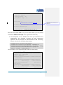
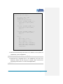
1.3 Product Features
1.3.1 Mini8510 Core Board
Figure 1: Back of MINI8510
Figure 2: Top of MINI8510
Operational Parameters:
Dimensions: 67x37mm
Operation Temperature: 0 ~ 70°C
Operating Humidity: 20% ~ 90% (Non-condensing)
Power Supply: 3.3V/0.17A
Processor:
TI DM3730 integrating a 1GHz ARM Cortex™-A8 core
800-MHz TMS320C64x+™ DSP
NEON™ SIMD co-processor
POWERVR SGX™ graphic accelerator
32KB instruction buffer, 32KB data buffer, 256KB L2 cache, 64KB
RAM and 32KB ROM
Page | 2
On-Board Memories:
256MB 32bit DDR SDRAM
512MB 16bit NAND Flash
Interfaces and Signals:
Camera interface (supports external CCD or CMOS camera)
JTAG interface
Two 1.27mm-pitch 90-pin DIP connectors
Six LED indicators (two power indicators and four custom user
indicators)
Two SPIs: SPI1 and SPI2
GPMC bus (16-bit data, 10-bit address, four CS and some control
signals)
Three UARTs (5-wire, support hardware flow control)
ULPI (USB1 HS)
Audio input and output
IIC bus (IIC3)
Two McBSPs: McBSP1 and McBSP3 (McBSP3 is multiplexed on
UART2)
Two MMCs/SDs:MMC1 (8-wire) and MMC2 (4-wire)
24-bit DSS interface
Page | 3
1.3.2 Expansion Board
Figure 3: SBC8140 Expansion Board
Operational Parameters:
Dimensions: 165x115mm
Operation temperature: 0 ~ 70°C
Operating Humidity: 20% ~ 90% (Non-condensing)
Power Supply: 5V/2A
Audio/Video Interfaces:
LCD/touch-screen interface (24-bit RGB full-colour output; 50-pin
FPC connector)
Standard VGA interface, supports 1024x768 resolution by default
Audio input interface (3.5mm audio jack)
Dual-channel audio output interface (3.5mm audio jack)
Data transfer interface:
Page | 4
10/100Mbps Ethernet interface (RJ45 connector)
High-speed USB 2.0 OTG interface with PHY (480Mbps mini-USB
interface)
Four high-speed USB 2.0 HOST interfaces with PHY (480Mbps
USB-A interface)
SD card slot (compatible with SD/MMC communication)
Serial Interfaces:
Interfaces
Descriptions
UART1
5-wire, RS232 voltage level, DB9 debugging serial interface
UART2
3-wire, TTL voltage level, 6-pin connector
UART3
5-wire, TTL voltage level, 6-pin connector
Input Interfaces:
BOOT button
Reset button
LED indicators:
Power indicator
Two custom user indicators
Page | 5
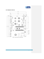
1.4 Interfaces on the SBC8140
Figure 4: SBC8140 Interfaces
Page | 6
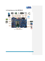
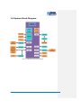
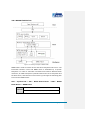
1.5 System Block Diagram
Figure 5: SBC8140 system block diagram
Page | 7
1.6 Hardware Dimensions
1.6.1 MINI8510 Core Board
Figure 6: MINI8510 dimensions (top side)
Figure 7: MINI8510 dimensions (back side)
Page | 8
1.6.2 Expansion Board
Figure 8: Expansion board dimensions
Page | 9
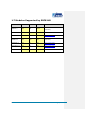
1.7 Modules Supported by SBC8140
Modules
Linux
Android
WinCE
Materials
Provided
with
CD-ROM
WF8000-U
Yes*
NO
Yes#
CAM8000-A
Yes*
Yes*
Yes*
Available in CD
CAM8000-D
Yes
NO
Yes*
Click to download
CAM8100-U
Yes*
Yes*
Yes
CDMA8000-U
Yes*
No
Yes
Click to download
WCDMA8000-U
Yes*
No
Yes
Click to download
LVDS8000
Yes*
Yes*
Yes*
Available on CD and website
Separately
Provided
with
CD-ROM
Separately
*=Source code provided
Page | 10
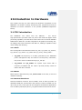
2 Introduction to Hardware
This chapter will help you learn about the hardware composition of the
MINI8510 core board by briefly introducing CPU, peripheral ICs and pin
definitions of various interfaces on the product (MINI8510+Expansion
board).
2.1 CPU Introduction
The
MINI8510
core
board
uses
the
DM3730
–
TI’s
45-nm
high-performance processor with low power and enhanced digital media
processing capability. The CPU has a 1GHz Cortex-A8 core and an 800MHz
TMS320C64+ DSP core, and also integrates a 3D graphics processing unit,
an imaging and video accelerator and USB 2.0, making it capable of 720p
video coding and decoding.
2.1.1 Clock
The clock signals of the DM3730 include sys_32k, sys_altclk, sys_clkout1,
sys_clkout2, sys_xtalout, sys_xtalin and sys_clkreq, among which:
sys_32k: the frequency is 32 KHz, generated by the TPS65930
power management chip and used for low-frequency calculation;
low-power mode is enabled through sys_32k pin.
sys_xtalou and sys_xtalin: are system input clocks with a
frequency of 26MHz and are used to provide primary clocks for
DPLLs and other modules.
2.1.2 Reset
Reset signal is determined by SYS_NRESPWRON of the CPU; a low level
validates resetting.
2.1.3 General Interfaces
General interfaces include 6 sets of GPIOs, each of which provides 32
dedicated GPIO pins, and therefore the total pin number of GPIOs can be
up to 192 (6×32). These pins can be configured for different applications
such as data input/output (driver), keypad interface and terminal control.
Page | 11
2.1.4 Display Subsystem
The display subsystem is used to provide an LCD or TV interface with logic
images which are stored in the frame buffer (SDRAM or SRAM); it is made
up of:
Display control (DISPC) module
Remote frame buffering interface (RFBI) module
I/O module and DSI protocol engine of the display serial interface
(DSI)
DSI PLLcontroller driver (DSI PLL and high-speed frequency divider
NTSC/PAL video codec
The display controller and DSI protocol engine are connected to the
internal bus of L3 and L4, while the RFBI and TV output codec module are
connected to the internal bus of L.
2.1.5 3D Graphics Acceleration System
The 2D/3D graphics acceleration system (SGX) can speed up 2D/3D
graphic applications. The SGX system is built on the POWERVR® SGX core
from Imagination Technologies. It is a new-generation of programmable
POWERVR graphics core. POWERVR SGX530 v1.2.5 has an adaptable
architecture which makes it suited for a wide range of applications from
main-stream mobile devices to high-end desk-top graphics processing. Its
target applications are mainly feature phones, PDAs and some portable
game consoles.
Page | 12
Figure 9: SGX Graphics Acceleration System
The architecture of the SGX graphics acceleration system allows for
switching among multiple threads by adopting two-level scheduling and
data partitioning, so that it is capable of processing pixels, vertexes, videos
and general data.
2.2 Peripheral ICs around CPU
2.2.1 TPS65930 Power Management IC
The TPS65930 is a power-management IC for OMAP families. The device
includes power-management, a USB high-speed transceiver, LED drivers,
an analogue-to-digital converter (ADC), a real-time clock (RTC), and
embedded power control (EPC). In addition, the TPS65930 includes a full
audio codec with two digital-to-analogue converters (DACs) and two ADCs
to implement dual voice channels, and a stereo downlink channel that can
play all standard audio sample rates through a multiple format
inter-integrated sound (I2S™)/time division multiplexing (TDM) interface.
Page | 13
The TPS65930 communicates with the CPU through the I2C protocol. It
supplies 1.2V and 1.8V to keep CPU working properly. Additionally, the
TPS65930 features Audio in, Audio out, OTG PHY, Keyboard, ADC and
GPIO functions.
2.2.2 H9DA4GH2GJAMCR Memory
The H9DA4GH2GJAMCR is a two-in-one memory which combines 512MB of
NAND Flash and 256MB of SDRAM DDR. The NAND Flash is accessed
through the GPMC bus, while the SDRAM is accessed through the
Controller (SDRC).
2.2.3 DM9000 Ethernet Controller
The DM9000 is a fully integrated fast Ethernet controller with a general
processor interface, a 10/100M PHY and 4K DWORD SRAM. It supports
3.3V with a 5V tolerance.
The SBC8140 uses the 10/100M self-adaptive network interface of the
DM8000 which is a standard RJ45 interface with connection and data
transfer indicators. The 10/100M Ethernet module integrated in the
DM9000 is compliant with the IEEE 802.3 standard.
The SBC8140 can be either connected to a hub with a straight-through
network cable, or to a PC with a cross-over network cable.
2.2.4 FE1.1 USB Hub
FE1.1 is a USB 2.0 high-speed 4-port hub solution. It uses the USB3320 to
provide 4 extended USB interfaces with support for high-speed (480MHz),
full-speed (2MHz) and low-speed (1.5MHz) modes.
2.2.5 TFP410 Flat Panel Display IC
The TFP410 is a Texas Instruments PanelBus flat panel display product,
part of a comprehensive family of end-to-end DVI 1.0-compliant solutions,
targeted at the PC and consumer electronics industry.
The TFP410 provides a universal interface to allow glue-less connection to
most commonly available graphics controllers. Some of the advantages of
this universal interface include selectable bus widths, adjustable signal
levels, and differential and single-ended clocking. The adjustable 1.1V to
1.8V digital interface provides a low-EMI, high-speed bus that connects
Page | 14
seamlessly with 12-bit or 24-bit interfaces. The DVI interface supports flat
panel display resolutions up to UXGA at 165 MHz in 24-bit true colour pixel
format.
2.2.6 MAX3232 Transceiver
The MAX3232 transceiver has a proprietary low-dropout transmitter
output stage enabling true RS-232 performance from a 3.0V to 5.5V
supply with a dual charge pump. The devices require only four small 0.1µF
external charge-pump capacitors. The MAX3232 is guaranteed to run at
data rates of 120kbps while maintaining RS-232 output levels.
The MAX3232 has 2 receivers and 2 drivers. It features a 1µA shutdown
mode that reduces power consumption and extends battery life in portable
systems. Its receivers remain active in shutdown mode, allowing external
devices such as modems to be monitored using only 1µA supply current.
The MAX3232 is pin, package, and functionally compatible with the
industry-standard MAX242 and MAX232, respectively. It is able to ensure
±5V transmission voltage which is the lowest requirement by RS-232
standard even when working at a high data rate.
The MAX3232 guarantees a 120kbps data rate with worst-case loads.
Typically, it can operate at a data rate of 235kbps. The transmitter can be
paralleled to drive multiple receivers or mice.
Page | 15
2.3 Hardware Interfaces and LEDs on
Mini8510
Figure 10: MINI8510
2.3.1 CN1 90pin DIP Interface (right row)
Pins
Definitions
Descriptions
1
GND1
GND
2
G_D14
GPMC data bit 14
3
G_D13
GPMC data bit 13
4
G_D10
GPMC data bit 10
5
G_D8
GPMC data bit 8
6
G_D9
GPMC data bit 9
7
G_D5
GPMC data bit 5
8
G_D7
GPMC data bit 7
9
G_D3
GPMC data bit 3
10
G_D6
GPMC data bit 6
11
G_D12
GPMC data bit 12
Page | 16
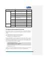
Pins
Definitions
Descriptions
12
G_D2
GPMC data bit 2
13
G_D11
GPMC data bit 11
14
G_D1
GPMC data bit 1
15
G_D4
GPMC data bit 4
16
G_D0
GPMC data bit 0
17
G_A2
GPMC address bit 2
18
G_A3
GPMC address bit 3
19
G_A1
GPMC address bit 1
20
G_A6
GPMC address bit 6
21
G_A4
GPMC address bit 4
22
G_A7
GPMC address bit 7
23
G_A5
GPMC address bit 5
24
G_A8
GPMC address bit 8
25
G_A9
GPMC address bit 9
26
G_D15
GPMC data bit 15
27
G_A10
GPMC address bit 10
28
GND2
GND
29
SPI2_CS1/GPT8
30
SPI2_CS10/GPT11
31
SPI2_SIMO/GPT9
32
SPI2_CLK
33
SPI2_SOMI GPT10
SPI Enable 1PWM or event for GP
timer 8
SPI Enable 0PWM or event for GP
timer 11
Slave data in, master data out PWM
or event for GP timer 9
SPI Clock
Slave data out, master data inPWM
or event for GP timer 10
Page | 17
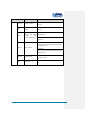
Pins
Definitions
Descriptions
34
SPI1_CS3
SPI Enable 3
35
SPI1_CS0
SPI Enable 0
36
SPI1_SIMO
Slave data in, master data out
37
SPI1_SOMI
Slave data out, master data in
38
SPI1_CLK
SPI Clock
39
GND3
GND
40
GPIO0
GPIO0 /card detection 1
41
MMC2_D2/SPI3_CS1
42
MMC2_D3/SPI3_CS0
43
MMC2_D0/SPI3_SOMI
44
MMC2_D1
MMC/SD Card Data bit 1
MMC2_CMD/SPI3_SIM
MMC/SD
O
data in, master data out
46
MMC2_CLK/SPI3_CLK
MMC/SD Output ClockSPI Clock
47
BSP3_DR/UART2_RTS
48
BSP3_CLK/UART2_TX
49
BSP3_FSX/UART2_RX
45
MMC/SD Card Data bit 2SPI Enable
1
MMC/SD Card Data bit 3SPI Enable
0
MMC/SD Card Data bit 0Slave data
out, master data in
command
signalSlave
Received serial dataUART2 Request
To Send
Combined
serial
clockUART2
Transmit data
Combined
synchronizationUART2
frame
Receive
data
Transmitted serial dataUART2 Clear
50
BSP3_DX/UART2_CTS
51
GND4
GND
52
UART1_CTS
UART1 Clear To Send
To Send
Page | 18
Pins
Definitions
Descriptions
53
UART1_TX
UART1 Transmit data
54
UART1_RX
UART1 Receive data
55
UART1_RTS
UART1 Request To Send
56
USB1HS_STP
57
USB1HS_D3
58
USB1HS_D5
59
USB1HS_6
60
USB1HS_D7
61
USB1HS_D1
62
USB1HS_D2
63
USB1HS_D4
64
USB1HS_D0
65
USB1HS_NXT
66
USB1HS_CLK
67
GND6
68
USB1HS_DIR
69
SYS_CLKOUT1
Dedicated for external transceiver
Stop signal
Dedicated for external transceiver
Bidirectional data bus
Dedicated for external transceiver
Bidirectional data bus
Dedicated for external transceiver
Bidirectional data bus
Dedicated for external transceiver
Bidirectional data bus
Dedicated for external transceiver
Bidirectional data bus
Dedicated for external transceiver
Bidirectional data bus
Dedicated for external transceiver
Bidirectional data bus
Dedicated for external transceiver
Bidirectional data bus
Dedicated for external transceiver
Next signal from PHY
Dedicated for external transceiver
60-MHz clock
GND
Dedicated for external transceiver
data form PHY
Configurable output clock1
Page | 19
Pins
Definitions
Descriptions
70
LEDA
LED leg A
71
LEDB
LED leg B
72
ADCIN0
ADC input0 (Battery type)
73
NRESPWRON
Power On Reset
74
NRESWARM
75
SYSEN
System enable output
76
GND6
GND
77
REGEN
Enable signal for external LDO
78
ADCIN1
79
KC0
Keypad column 0
80
KC1
Keypad column 0
81
KC2
Keypad column 0
82
KC3
Keypad column 0
83
AUDIO_IN
Analogue microphone bias 1
84
AUDIO_OR
85
AUXR
86
AUDIO_OL
87
GND7
GND
88
VBAT1
Power supply (3V - 4.2V 1.5A)
89
ON/OFF
90
VBAT2
Warm
Boot
Reset
(open
drain
output)
ADC input1 (General-purpose ADC
input)
Predriver output right P for external
class-D amplifier
Auxiliary audio input right
Predriver output left P for external
class-D amplifier
Input; detect a control command to
start or stop the system
Power supply (3V - 4.2V 1.5A)
Page | 20
2.3.2 CN2 90pin DIP Interface (left row)
Pins
Definitions
Descriptions
1
G_NWE
GPMC Write Enable
2
G_NOE
GPMC Read Enable
GPMC Chip Select bit 7PWM / event
3
G_NCS7/GPT8/G_DIR
for GP timer 8GPMC / IO direction
control
for
use
with
external
transceivers
GPMC Chip Select bit 7PWM /DMA
4
G_NCS4/DMAREQ1
5
G_NCS6/DMAREQ3
6
G_NCS3DMAREQ0
7
GND1
GND
8
G_WAIT0
External indication of wait
9
G_NBE0 / G_CLE
10
G_ALE
Address Latch Enable
11
G_NBE1
Upper Byte Enable
12
HDQ_SIO
13
MMC1_D0
MMC/SD Card Data bit 0
14
MMC1_D1
MMC/SD Card Data bit 1
15
MMC1_D2
MMC/SD Card Data bit 2
16
MMC1_D6/IO128
MMC/SD Card Data bit 6
17
MMC1_D5/IO127
MMC/SD Card Data bit 5
18
MMC1_D4/IO126
MMC/SD Card Data bit 4
19
MMC1_D7/IO129
MMC/SD Card Data bit 7
request 1
GPMC Chip Select bit 7PWM / DMA
request 3
GPMC Chip Select bit 7External
DMA request 0
Lower Byte Enable. Also used for
Command Latch Enable
Bidirectional HDQ 1-Wire control
and data
Page | 21
Pins
Definitions
Descriptions
20
MMC1_D3
MMC/SD Card Data bit 3
21
GND2
GND
22
MMC1_CLK
MMC/SD Output Clock
23
MMC1_CMD
MMC/SD command signal
24
VMMC1
25
UART3_RX
UART3 Receive data
26
UART3_CTS
UART3 Clear To Send
27
UART3_TX
UART3 Transmit data
28
UART3_RTS
UART3 Request To Send
29
DSS_ACBIAS
30
DSS_VSYNC
LCD Vertical Synchronization
31
GND3
GND
32
DSS_HSYNC
LCD Horizontal Synchronization
33
DSS_CLK
LCD Pixel Clock
34
DSS_D6
LCD Pixel Data bit 6
35
DSS_D8
LCD Pixel Data bit 8
36
DSS_D7
LCD Pixel Data bit 7
37
DSS_D9
LCD Pixel Data bit 9
38
DSS_D20
LCD Pixel Data bit 20
39
DSS_D17
LCD Pixel Data bit 17
40
DSS_D16
LCD Pixel Data bit 16
41
DSS_D18
LCD Pixel Data bit 18
42
DSS_D10
LCD Pixel Data bit 10
Power supply for SD/MMC1 (3.0 /
1.8V)
AC bias control (STN) or pixel data
enable (TFT) output
Page | 22
Pins
Definitions
Descriptions
43
DSS_D5
LCD Pixel Data bit 5
44
DSS_D4
LCD Pixel Data bit 4
45
GND4
GND
46
DSS_D2
LCD Pixel Data bit 2
47
DSS_D3
LCD Pixel Data bit 3
48
DSS_D0
LCD Pixel Data bit 0
49
DSS_D15
LCD Pixel Data bit 15
50
DSS_D11
LCD Pixel Data bit 11
51
DSS_D23
LCD Pixel Data bit 23
52
DSS_D22
LCD Pixel Data bit 22
53
DSS_D14
LCD Pixel Data bit 14
54
DSS_D19
LCD Pixel Data bit 19
55
DSS_D13
LCD Pixel Data bit 13
56
DSS_D21
LCD Pixel Data bit 21
57
DSS_D1
LCD Pixel Data bit 1
58
DSS_D12
LCD Pixel Data bit 12
59
GND5
GND
60
MCBSP1_FSR/IO157
Receive frame synchronization
61
MCBSP1_CLKR/IO156
Receive Clock
62
MCBSP1_FSX/IO161
Transmit frame synchronization
63
MCBSP1_CLKS/IO160
External clock input
64
MCBSP1_CLKX/IO162
Transmit clock
65
MCBSP1_DR/IO159
Received serial data
66
MCBSP1_DX/IO158
Transmitted serial data
Page | 23
Pins
Definitions
Descriptions
67
GND6
GND
68
TV_OUTC
69
TV_OUTY
70
VDD33_1
71
IIC3_SCL
72
IIC3_SDA
73
IO25
General-purpose IO 183
74
IO27
General-purpose IO 183
75
BOOTJUMP
Boot configuration mode bit 5.
76
GND7
GND
77
VBUS
VBUS power rail (5V 10mA)
78
USB_DN
USB Data N
79
USB_ID
USB ID
80
USB_DP
USB Data P
81
PWM0
Pulse width driver 0
82
KR0
Keypad row 0
83
KR1
Keypad row 1
84
KR2
Keypad row 2
85
KR3
Keypad row 3
86
KR4
Keypad row 4
87
VDD18_1
TV
analogue
output
S-VIDEO:
TV_OUT2
TV analogue output Composite:
TV_OUT1
Power supply for camera (3.3V
500mA )
I2C Master Serial clock. Output is
open drain
I2C
Serial
Bidirectional
Data.
Output is open drain
Power supply from TPS65930 (VIO
1.8V)
Page | 24
Pins
Definitions
88
GND8
89
VDD18_2
90
BKBAT
Descriptions
GND
Power supply from TPS65930 (VIO
1.8V)
Backup battery
2.3.3 CN3 JTAG Interface
Pins
Definitions
Descriptions
1
VDD18
1.8V output
2
TMS
Test mode select
3
TD1
Test data input
4
NTRST
Test system reset
5
TD0
Test data output
6
RTCK
Receive test clock
7
TCK
Test clock
8
EMU0
Test emulation 0
9
EMU1
Test Emulation 1
10
GND
GND
2.3.4 CN4 Camera Interface
Pins
Definitions
Descriptions
1
GND0
GND
2
D0
Digital image data bit 0
3
D1
Digital image data bit 1
4
D2
Digital image data bit 2
5
D3
Digital image data bit 3
Page | 25
Pins
Definitions
Descriptions
6
D4
Digital image data bit 4
7
D5
Digital image data bit 5
8
D6
Digital image data bit 6
9
D7
Digital image data bit 7
10
D8
Digital image data bit 8
11
D9
Digital image data bit 9
12
D10
Digital image data bit 10
13
D11
Digital image data bit 11
14
GND1
GND
15
PCLK
Pixel clock
16
GND2
GND
17
HS
Horizontal synchronization
18
VDD50
5V
19
VS
Vertical synchronization
20
VDD33
3.3V
21
XCLKA
Clock output a
22
XCLKB
Clock output b
23
GND3
GND
24
FLD
Field identification
25
WEN
Write Enable
26
STROBE
Flash strobe control signal
27
SDA
IIC master serial clock
28
SCL
IIC serial bidirectional data
29
GND4
GND
Page | 26
Pins
30
Definitions
VDD18
Descriptions
1.8V
2.3.5 LED Indicators
LEDs
Definitions
Descriptions
D1
LED1
User custom LED
D2
LED2
User custom LED
D3
LED3
User custom LED
D4
LED4
User custom LED
D5
VDD18
Power indicator
D6
VBAT
Power indicator
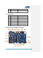
2.4 Interfaces on Expansion Board
Figure 11: Expansion Board
Page | 27
2.4.1 Power Jack
Pins
Definitions
Descriptions
1
GND
GND
2
+5V
Power supply (+5V) 2A (Type)
2.4.2 TFT_LCD Interface
Pins
Definitions
Descriptions
1
DSS_D0
LCD Pixel data bit 0
2
DSS_D1
LCD Pixel data bit 1
3
DSS_D2
LCD Pixel data bit 2
4
DSS_D3
LCD Pixel data bit 3
5
DSS_D4
LCD Pixel data bit 4
6
DSS_D5
LCD Pixel data bit 5
7
DSS_D6
LCD Pixel data bit 6
8
DSS_D7
LCD Pixel data bit 7
9
GND
GND
10
DSS_D8
LCD Pixel data bit 8
11
DSS_D9
LCD Pixel data bit 9
12
DSS_D10
LCD Pixel data bit 10
13
DSS_D11
LCD Pixel data bit 11
14
DSS_D12
LCD Pixel data bit 12
15
DSS_D13
LCD Pixel data bit 13
16
DSS_D14
LCD Pixel data bit 14
17
DSS_D15
LCD Pixel data bit 15
18
GND
GND
Page | 28
Pins
Definitions
Descriptions
19
DSS_D16
LCD Pixel data bit 16
20
DSS_D17
LCD Pixel data bit 17
21
DSS_D18
LCD Pixel data bit 18
22
DSS_D19
LCD Pixel data bit 19
23
DSS_D20
LCD Pixel data bit 20
24
DSS_D21
LCD Pixel data bit 21
25
DSS_D22
LCD Pixel data bit 22
26
DSS_D23
LCD Pixel data bit 23
27
GND
GND
28
DEN
29
HSYNC
LCD Horizontal Synchronization
30
VSYNC
LCD Vertical Synchronization
31
GND
GND
32
CLK
LCD Pixel Clock
33
GND
GND
34
X+
X+ Position Input
35
X-
X- Position Input
36
Y+
Y+ Position Input
37
Y-
Y- Position Input
38
SPI_CLK
SPI clock
39
SPI_MOSI
Slave data in, master data out
40
SPI_MISO
Slave data out, master data in
41
SPI_CS
SPI enable
42
IIC_CLK
IIC master serial clock
AC bias control (STN) or pixel data
enable (TFT)
Page | 29
Pins
Definitions
Descriptions
43
IIC_SDA
IIC serial bidirectional data
44
GND
GND
45
VDD18
1.8V
46
VDD33
3.3V
47
VDD50
5V
48
VDD50
5V
49
RESET
Reset
50
PWREN
Power on enable
Page | 30
2.4.3 Audio Output Interface
Pins
Definitions
Descriptions
1
GND
GND
2
NC
NC
3
Right
Right output
4
NC
NC
5
Left
Left output
2.4.4 Audio Input Interface
Pins
Definitions
Descriptions
1
GND
GND
2
NC
NC
3
MIC MAIN P
Right input
4
NC
NC
5
MIC MAIN N
Left input
2.4.5 Serial Interface
Pins
Definitions
Descriptions
1
NC
NC
2
RXD
Receive data
3
TXD
Transit data
4
NC
NC
5
GND
GND
6
NC
NC
7
RTS
Request To Send
Page | 31
Pins
Definitions
Descriptions
8
CTS
Clear To Send
9
NC
NC
2.4.6 Ethernet Interface
Pins
Definitions
Descriptions
1
TX+
TX+ output
2
TX-
TX- output
3
RX+
RX+ input
4
VDD25
2.5V Power for TX/RX
5
VDD25
2.5V Power for TX/RX
6
RX-
RX- input
7
NC
NC
8
NC
NC
9
VDD
3.3V Power for LED
10
LED1
Speed LED
11
LED2
Link LED
12
VDD
3.3V Power for LED
2.4.7 USB OTG Interface
Pins
Definitions
Descriptions
1
VBUS
+5V
2
DN
USB Data-
3
DP
USB Data+
4
ID
USB ID
Page | 32
Pins
5
Definitions
GND
Descriptions
GND
2.4.8 USB HOST Interface
Pins
Definitions
Descriptions
1
VBUS
+5V
2
DN
USB Data-
3
DP
USB Data+
4
ID
USB ID
2.4.9 SD Card Interface
Pins
Definitions
Descriptions
1
CD/DAT3
Card detect/Card data 2
2
DCMD
Command Signal
3
VSS
GND
4
VDD
VDD
5
CLK
Clock
6
VSS
GND
7
TF_DAT0
Card data 0
8
TF_DAT1
Card data 1
9
TF_DAT2
Card data2
10
SW_2
SD write protect
11
SW_1
Card detect
12
GND
GND
Page | 33
2.4.10 LED Indicators
LEDs
Definitions
Descriptions
D4
LED_POWER
3.3V power indicator
D5
User LED
User custom LED
2.4.11 Buttons
Buttons
Definitions
Descriptions
CN12
BOOTJUMP
Boot system from TF card
CN11
Reset
Reset system
Page | 34
3 Linux Operating System
The SBC8140 has a complete Linux system (with 4.3” LCD support)
preinstalled in its on-board NAND Flash. This chapter contains several
sections to introduce the Linux system of the SBC8140 in detail, including
the structure of the embedded Linux system, software features, system
development process, driver introduction and development, and system
updating.
Note:
Some instructions have been proceeded by an icon “” to prevent confusion
caused by the long instructions that occupy more than one line.
Ubuntu Linux is used in this document. If you do not have a Linux system on
your PC, please refer to Installing an Ubuntu Linux.
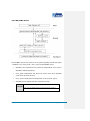
3.1 Structure of the Embedded Linux System
The following figure shows the structure of the embedded Linux system:
Figure 12: Embedded Linux System
x-loader: First-level booting program; after the kit is powered on,
the program is copied from the ROM in CPU to RAM and executed so
as to initialize the CPU and copy u-boot to RAM, and then u-boot
takes control over the system,
Page | 35
u-boot: Second-level booting program; it is used to interact with
users and provide functions such as updating image files and
booting the core.
Kernel: Core 2.6.32 version; customized for the SBC8140.
Roofs: Open source ubifs file system; it is suited for embedded
systems.
3.2 Software Features
Software
x-loader
BIOS
Descriptions
Code Type
NAND / ONENAND
Source code
MMC/SD
Source code
FAT
Source code
NAND / ONENAND
Source code
MMC/SD
Source code
FAT
Source code
NET
Source code
u-boot
Supports
Kernel
Linux-2.6.x
ROM/CRAM/EXT2/EXT3/FAT/NFS/
Source code
JFFS2/UBIFS filesystems
Device Driver
serial
Serial interface driver
Source code
rtc
Hardware clock driver
Source code
net
10/100M Ethernet DM9000 driver
Source code
flash
NAND flash driver (supports NAND
boot)
Source code
lcd
TFT LCD driver
Source code
touch screen
Touch-screen controller ads7846 driver
Source code
mmc/sd
MMC/SD controller driver
Source code
Page | 36
Software
usb otg
Descriptions
Code Type
USB OTG 2.0 driver (currently only
supports USB device mode)
Source code
usb ehci
USB ehci driver
Source code
VGA
Supports VGA signal output
Source code
audio
Sound
card
driver
(support
recording/playback)
audio
Source code
camera
Camera driver
Source code
Key
Key driver
led
LEDs driver
Source code
Android
Android system v2.2
Source code
DVSDK
DVSDK 4_00_00_22 system
Source code
Demo
3.3 System Development Process
This section will show you the whole process of developing software
starting from building a development environment to making a customized
system.
3.3.1 Building Development Environment
1. Installing Cross Compilation Tools;
Put the DVD-ROM in your PC’s DVD drive, Ubuntu will mount it under
/media/cdrom/ automatically, and then execute the following instructions
in the terminal window of Ubuntu to uncompress the cross compiling tools
from /media/cdrom/linux/tools to $HOME;
cd /media/cdrom/linux/tools
tar xvf arm-eabi-4.4.0.tar.bz2 -C $HOME
tar xvf arm-2007q3.tar.bz2 -C $HOME
2. Copying More Tools;
Continue executing the following instructions to copy the tools required
during source code compilation from /linux/tools to $HOME/tools/;
Page | 37
mkdir $HOME/tools
cp /media/cdrom/linux/tools/mkimage $HOME/tools
cp /media/cdrom/linux/tools/signGP $HOME/tools
cp /media/cdrom/linux/tools/mkfs.ubifs $HOME/tools
cp /media/cdrom/linux/tools/ubinize $HOME/tools
cp /media/cdrom/linux/tools/ubinize.cfg $HOME/tools
3. Adding Environment Variables;
Execute the following instructions to add installed tools into the
environment variables;
export
PATH=$HOME/arm-eabi-4.4.0/bin:$HOME
/arm-2007q3/bin:$HOME/tools:$PATH
Note:
The instructions used to add environment variables can be put into the file
.bashrc under user directory to allow the system to load the variable
automatically each time it boots up.
If you need to view the path, please use the instruction echo $PATH.
3.3.2 System Compilation
1. Uncompress Source Code;
Execute the following instructions to uncompress the source code from
/linux/source of DVD-ROM to the Ubuntu system;
mkdir $HOME/work
cd $HOME/work
tar xvf /media/cdrom/linux/source/x-loader-03.00.02.07.tar.bz2
tar xvf /media/cdrom/linux/source/u-boot-03.00.02.07.tar.bz2
tar xvf /media/cdrom/linux/source/linux-2.6.32-sbc8140.tar.bz2
sudo tar xvf /media/cdrom/linux/source/rootfs.tar.bz2
tar
xvf
/media/cdrom/linux/demo/Android/source/rowboat-android-froyo-sbc8140
.tar.bz2
Page | 38
After
all
the
instructions
are
executed,
the
directories
x-loader-03.00.02.07, u-boot-03.00.02.07, linux-2.6.32-sbc8140, rootfs
and rowboat-android-froyo-sbc8140 are created under current directory.
2. Compiling First-Level Booting Code;
Execute the following instructions to compile the first-level booting code
for SD card boot-up mode;
cd x-loader-03.00.02.07
make distclean
make omap3sbc8140_config
make
signGP x-load.bin
mv x-load.bin.ift MLO
After all the instructions are executed, a MLO file is generated in the
current directory.
Execute the following instructions to compile first-level code for NAND
Flash boot-up mode;
cd x-loader-03.00.02.07
vi include/configs/omap3sbc8140.h
Note:
cd x-loader-03.00.02.07
make distclean
with the line // #define
CONFIG_MMC
make omap3sbc8140_config
1 in the
file omap3sbc8140.h
make
signGP x-load.bin
mv x-load.bin.ift x-load.bin.ift_for_NAND
After
all
the
instructions
are
executed,
a
file
named
x-load.bin.ift_for_NAND is generated in the current directory.
3. Compiling Second-Level Code;
Execute the following instructions to compile the second-level booting
code;
cd u-boot-03.00.02.07
make distclean
make omap3_sbc8140_config
make
After all the instructions are executed, a file named u-boot.bin is generated
in the current directory.
Page | 39
4. Compiling Kernel;
The operations for a Linux system are as follows:
cd linux-2.6.32-sbc8140
make distclean
make omap3_sbc8140_defconfig
make uImage
The operations for an Android system are as follows:
cd linux-2.6.32-sbc8140
make distclean
make omap3_sbc8140_android_defconfig
make uImage
After the above operations are executed, the uImage file will be generated
in the directory arch/arm/boot.
5. Making Filesystem;
To make a Ramdisk filesystem please visit:
http://www.elinux.org/DevKit8600_FAQ.
Execute the following instructions to generate a UBI file;
cd $HOME/work
sudo $HOME/tools/mkfs.ubifs -r rootfs -m 2048 -e 129024 -c 1996 -o
ubifs.img
sudo
$HOME/tools/ubinize
-o
ubi.img
-m
2048
-p
128KiB
-s
512
$HOME/tools/ubinize.cfg
After all the instructions are executed, a file ubi.img is generated in the
current directory.
6. Android system compilation
Execute the following instructions to start the compilation of an Android
system;
cd rowboat-android-froyo-SBC8140
make
Please enter the following instructions to start making a ubi file system;
source ./build_ubi.sh
The generated file: ubi.img, can be found under temp/.
Page | 40
Note:
Before the compilation of an Android file system, the Android kernel source
code linux-2.6.32-sbc8140 needs to be compiled first, or errors might occur
during the process.
3.3.3 Customizing the System
There are many configurations available for users to add or remove drivers
and features in the Linux core so as to meet requirements. The following
example shows the process of making a custom system.
1. Entering Configuration Menu;
By
default,
the
configuration
file
is
saved
under
/linux-2.6.32-sbc8140/arch/arm/configs/omap3_SBC8140_defconfig/;
please execute the following instructions to enter the system configuration
menu;
cd linux-2.6.32-sbc8140
cp arch/arm/configs/omap3_sbc8140_defconfig .config
make menuconfig
Notice:
If errors occur when executing make menuconfig, one possible cause is that the
ncurses library is missing in the Ubuntu system. Type sudo apt-get install
ncurses-dev into the terminal to install the library.
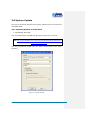
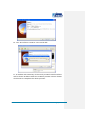
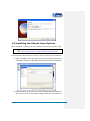
2. Customizing Configurations;
Change configurations according to actual requirements, for example
select Device Drivers > USB support > USB Gadget Support > USB Gadget
Drivers and check File-backed Storage Gadget as shown below, and
then exit and save changes.
Page | 41
Figure 13: USB Gadget Drivers submenu
Set the option File-backed Storage Gadget to M, and then exit and save
changes.
3. Execute the following instructions to compile the core;
make uImage
make modules
After the instructions are executed, a core image file named uImage and a
module file g_file_storage.ko are generated under /arch/arm/boot/ and
/drivers/usb/gadget/ respectively.
3.4 Introduction to Drivers
This section will introduce various drivers required in a Linux system,
including NAND Flash, SD/MMC, display subsystem, video capture and
audio input/output drivers.
The following table contains the paths for all the drivers;
Software
Description
ONENAND
NAND
BIOS
x-loader
Paths
x-loader-03.00.02.07/drivers/onenand.c
x-loader-03.00.02.07/drivers/k9f1g08r0a.
c
MMC/SD
x-loader-03.00.02.07/cpu/omap3/mmc.c
FAT
x-loader-03.00.02.07/fs/fat/
Page | 42
Software
u-boot
Description
Paths
NAND
u-boot-03.00.02.07/drivers/mtd/nand/
ONENAND
u-boot-03.00.02.07/drivers/mtd/onenand/
MMC/SD
u-boot-03.00.02.07/drivers/mmc
FAT
u-boot-03.00.02.07/fs/fat/
u-boot-03.00.02.07/drivers/net/dm9000x.
NET
c
Supports
Kernel
Linux-2.6
.x
ROM/CRAM/EXT2/EX
T3/FAT/NFS/
linux-2.6.32-sbc8140/fs/
JFFS2/UBIFS
filesystems
linux-2.6.32-sbc8140/drivers/serial/8250.
serial
Serial interface driver
rtc
Hardware clock driver
linux-2.6.32-sbc8140/drivers/rtc/rtc-twl.c
10/100M
linux-2.6.32-sbc8140/drivers/net/dm9000
net
flash
Ethernet
DM9000 driver
NAND
flash
c
.c
driver
(supports nand boot)
linux-2.6.32-sbc8140/drivers/mtd/nand/o
map2.c
linux-2.6.32-sbc8140/drivers/video/omap
2/omapfb/omapfb-main.c
Device
lcd
TFT LCD driver
linux-2.6.32-sbc8140/drivers/video/omap
Driver
2/displays/panel-omap3-sbc8140.c
touch
screen
mmc/sd
Touch-screen
controller
ads7846
driver
MMC/SD
controller
driver
linux-2.6.32-sbc8140/drivers/input/touchs
creen/ads7846.c
linux-2.6.32-sbc8140/drivers/mmc/host/o
map_hsmmc.c
USB OTG 2.0 driver
usb otg
(currently
only
supports USB device
linux-2.6.32-sbc8140/drivers/usb/otg/twl4
030-usb.c
mode)
Page | 43
Software
usb ehci
VGA
Description
Paths
linux-2.6.32-sbc8140/drivers/usb/host/eh
USB ehci driver
ci-hcd.c
Support VGA signal
linux-2.6.32-sbc8140/drivers/i2c/chips/ch
output
7033.c
linux-2.6.32-sbc8140/sound/soc/omap/om
Sound
audio
card
(support
driver
ap3sbc8140.c
audio
recording/playback)
linux-2.6.32-sbc8140/sound/soc/codecs/t
wl4030.c
Digital:
linux-2.6.32-sbc8140/drivers/media/video
/omap34xxcam.c
camera
Camera driver
Catalogue:
linux-2.6.32-sbc8140/drivers/media/video
/tvp514x-int.c
Keypad
keypad driver
LED
LED driver
linux-2.6.32-sbc8140/drivers/input/keybo
ard/gpio_keys.c
linux-2.6.32-sbc8140/drivers/leds/leds-gpi
o.c
Page | 44
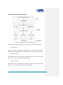
3.4.1 NAND Flash Driver
Figure 14: Working Principle of NAND Flash
NAND flash is used as a block device and has a filesystem built into it. The
interaction between users and NAND Flash is facilitated by a specific
filesystem. In order to eliminate inconsistencies between different flash
memories, an MTD subsystem is placed between the core’s filesystem and
the flash driver, and therefore users need to go through the following path
to access the NAND Flash:
User > System Call > VFS > Block Device Driver > MTD > NAND
Flash Driver > NAND Flash
linux-2.6.32-sbc8140/drivers/mtd/nand/
Reference
linux-2.6.32-sbc8140/drivers/mtd/nand/omap2.c
Page | 45
3.4.2 SD/MMC Driver
Figure 15: Working Principle of SD/MMC
The SD/MMC card drivers under a Linux system typically include four parts
- SD/MMC core, mmc_block, mmc_queue and SD/MMC driver;
SD/MMC core implements the structure independent core code in
SD/MMC related operations;
mmc_block implements the driver structure used when SD/MMC
cards work as block devices;
mmc_queue implements management of the request queue;
SD/MMC driver implements the controller drivers;
linux-2.6.32-sbc8140/drivers/mmc/
Reference
linux-2.6.32-sbc8140/drivers/mmc/host/omap_hsmmc.c
Page | 46
3.4.3 Display Subsystem Driver
Figure 16: Working Principle of Display Subsystem
The hardware of the display subsystem includes a graphics channel, two
video channels and two overlay management units; one of the units is
responsible for the digital interface, another for the analogue interface.
The digital interface manages the LCD output, while the analogue one
manages the TV output.
The main function of a display driver is to provide interfaces for the upper
application layer and manage the hardware components of the display
subsystem.
linux-2.6.32-sbc8140/drivers/video/omap2/
Reference
linux-2.6.32-sbc8140/drivers/video/omap2/omapfb/omapfb-main.c
linux-2.6.32-sbc8140/drivers/video/omap2/displays/panel-omap3-sbc8140.c
Page | 47
3.4.4 Video Capture Driver
Figure 17: Working Principle of Video Capture
V4L2 Subsystem:
The V4L2 subsystem of a Linux system works as the medium layer which
helps access the camera driver. The upper-layer applications of the camera
can access drivers through the API of the V4L2. The V4L2 subsystem of the
Linux 2.6 core is designed based on the V4L2 standard.
Video Buffer Library:
The Video Buffer Library is a part of the V4L2. It provides an assistance
function to effectively manage the video buffer via a queuing method.
Camera Driver:
The Camera driver allows external codecs to capture video images. It is
registered to layer V4L2 as a master device. Any codec driver that is added
to layer V4L2 as a slave device will be associated with the camera
controller driver through a new V4L2 master-slave interface. Currently the
Page | 48
driver can support only one codec device associated a with camera
controller.
Codec Driver:
The Codec driver needs to comply with the V4L2 master-slave interface
standard and should be registered to the V4L2 as a slave device. Replacing
the codec can be accomplished by rewriting the codec driver, without any
change to the camera driver.
CCDC Library:
As a hardware module for data input, the CCDC receives data from
sensors/decoders. The CCDC library provides an API for configuring the
CCDC module and being called by camera driver.
linux-2.6.32-sbc8140/drivers/media/video/
Reference
linux-2.6.32-sbc8140/drivers/media/video/omap34xxcam
.c
linux-2.6.32-sbc8140/drivers/media/video/tvp514x-int.c
Page | 49
3.4.5 Audio Input/Output Driver
Figure 18: Working principle of audio input/output
The ASoC embedded audio system is comprised of the following parts;
Codec Driver:
The codec driver is platform independent and contains audio controls,
audio interface capabilities, codec DAPM definition and codec IO functions.
Platform Driver:
The Platform driver contains the audio DMA engine and audio interface
drivers (e.g. I2S, AC97, PCM) for that platform.
Machine Driver:
The Machine driver handles any machine specific controls and audio
events. I.e. turning on an amp at start of playback.
Page | 50
linux-2.6.32-sbc8140/sound/soc/
Reference
linux-2.6.32-sbc8140/sound/soc/omap/omap3sbc8140.c
linux-2.6.32-sbc8140/sound/soc/codecs/twl4030.c
3.5 Driver Development
This section will introduce how to develop drivers with two examples,
GPIO_Keys and GPIO_LEDs.
3.5.1 GPIO_Keys Driver
1. Device Definition;
The
source
file:
board-omap3sbc8140.c
is
saved
under
/linux-2.6.32-sbc8140/arch/arm/mach-omap2/;
static struct gpio_keys_button gpio_buttons[] = {
{
.code
= KEY_F1,
.gpio
= 26,
.desc
= "menu",
.active_low
= true,
},
{
.code
= KEY_ESC,
.gpio
= 29,
.desc
= "back",
.active_low
= true,
},
};
static struct gpio_keys_platform_data gpio_key_info = {
.buttons
= gpio_buttons,
.nbuttons
= ARRAY_SIZE(gpio_buttons),
};
static struct platform_device keys_gpio = {
.name
= "gpio-keys",
.id
= -1,
.dev
= {
Page | 51
.platform_data = &gpio_key_info,
},
};
Set GPIO 26 as the menu key, returning the key value KEY_F1, triggered
by a low voltage level.
2. GPIO pinmux Configuration;
The
file
sbc8140.h
is
saved
under
/u-boot-03.00.02.07/board/timll/sbc8140/;
/*
* IEN
- Input Enable
* IDIS - Input Disable
* PTD
- Pull type Down
* PTU
- Pull type Up
* DIS
- Pull type selection is inactive
* EN
- Pull type selection is active
* M0
- Mode 0
* The commented string gives the final mux configuration for
that pin
*/
MUX_VAL(CP(ETK_D12_ES2),
(IEN
| PTU | DIS | M4))
(IEN
| PTU | DIS | M4))
/*GPIO_26*/\
MUX_VAL(CP(ETK_D15_ES2),
/*GPIO_29*/\
Set GPIOs 26 and 29 as M4 (GPIO mode) and IEN (allow input).
3. Driver Design;
The
source
file:
gpio_keys.c
is
saved
under
/linux-2.6.32-sbc8140/drivers/input/keyboard/;
Call platform_driver_register to register gpio_keys driver;
static struct platform_driver gpio_keys_device_driver = {
.probe
= gpio_keys_probe,
.remove
= __devexit_p(gpio_keys_remove),
.driver
.name
= {
= "gpio-keys",
Page | 52
.owner
= THIS_MODULE,
#ifdef CONFIG_PM
.pm
= &gpio_keys_pm_ops,
#endif
}
};
static int __init gpio_keys_init(void)
{
return
platform_driver_register(&gpio_keys_device_driver);
}
static void __exit gpio_keys_exit(void)
{
platform_driver_unregister(&gpio_keys_device_driver);
}
module_init(gpio_keys_init);
module_exit(gpio_keys_exit);
MODULE_LICENSE("GPL");
MODULE_AUTHOR("Phil Blundell <[email protected]>");
MODULE_DESCRIPTION("Keyboard driver for CPU GPIOs");
MODULE_ALIAS("platform:gpio-keys");
Call input_register_device to register input driver;
static int __devinit gpio_keys_probe(struct platform_device
*pdev)
{
…
input = input_allocate_device();
…
for (i = 0; i < pdata->nbuttons; i++) {
struct
gpio_keys_button
*button
=
gpio_button_data
*bdata
=
&pdata->buttons[i];
struct
&ddata->data[i];
unsigned int type = button->type ?: EV_KEY;
bdata->input = input;
Page | 53
bdata->button = button;
error = gpio_keys_setup_key(dev, bdata, button);
if (error)
goto fail2;
if (button->wakeup)
wakeup = 1;
input_set_capability(input,
type,
button->code);
}
error = input_register_device(input);
…
Apply for GPIO, set GPIO as input, and register GPIO interrupt;
static int __devinit gpio_keys_setup_key(struct device *dev,
struct
gpio_button_data
struct
gpio_keys_button
*bdata,
*button)
{
char *desc = button->desc ? button->desc : "gpio_keys";
int irq, error;
setup_timer(&bdata->timer, gpio_keys_timer, (unsigned
long)bdata);
INIT_WORK(&bdata->work, gpio_keys_work_func);
error = gpio_request(button->gpio, desc);
if (error < 0) {
dev_err(dev, "failed to request GPIO %d, error
%d\n",
button->gpio, error);
goto fail2;
}
error = gpio_direction_input(button->gpio);
if (error < 0) {
dev_err(dev, "failed to configure"
Page | 54
" direction for GPIO %d, error %d\n",
button->gpio, error);
goto fail3;
}
irq = gpio_to_irq(button->gpio);
if (irq < 0) {
error = irq;
dev_err(dev, "Unable to get irq number for GPIO
%d, error %d\n",
button->gpio, error);
goto fail3;
}
error = request_irq(irq, gpio_keys_isr,
IRQF_SHARED |
IRQF_TRIGGER_RISING
|
IRQF_TRIGGER_FALLING,
desc, bdata);
if (error) {
dev_err(dev, "Unable to claim irq %d; error %d\n",
irq, error);
goto fail3;
}
return 0;
fail3:
gpio_free(button->gpio);
fail2:
return error;
}
Interrupt processing; an interrupt is generated when pressing a button,
and then a key value will be returned;
static irqreturn_t gpio_keys_isr(int irq, void *dev_id)
{
…
schedule_work(&bdata->work);
…
}
Page | 55
static void gpio_keys_work_func(struct work_struct *work)
{
…
gpio_keys_report_event(bdata);
…
}
static void gpio_keys_report_event(struct gpio_button_data
*bdata)
{
struct gpio_keys_button *button = bdata->button;
struct input_dev *input = bdata->input;
unsigned int type = button->type ?: EV_KEY;
int state = (gpio_get_value(button->gpio) ? 1 : 0) ^
button->active_low;
input_event(input, type, button->code, !!state);
input_sync(input);
3.5.2 GPIO_LEDs Driver
1. Device Definitions;
The
source
file:
board-omap3sbc8140.c
is
saved
under
/linux-2.6.32-sbc8140/arch/arm/mach-omap2/;
static struct gpio_led gpio_leds[] = {
{
.name
.default_trigger
.gpio
.active_low
= "led0",
= "heartbeat",
= 136,
= true,
},
{
.name
= "led1",
.gpio
= 137,
/* gets replaced
*/
.active_low
= true,
},
{
.name
= "led2",
.gpio
= 138,
/* gets replaced
Page | 56
*/
.active_low
= true,
},
{
.name
= "led3",
.gpio
= 139,
/* gets replaced
*/
.active_low
= true,
},
};
Associates GPIO 136 with led0 (system breath LED), GPIO 137 with led1,
GPIO 138 with led2, and GPIO 139 with led3; they are all valid upon a low
voltage level.
2. GPIO pinmux Configurations;
The
file:
sbc8140.h
is
saved
under
/u-boot-03.00.02.07/board/timll/sbc8140/;
/*
* IEN
- Input Enable
* IDIS - Input Disable
* PTD
- Pull type Down
* PTU
- Pull type Up
* DIS
- Pull type selection is inactive
* EN
- Pull type selection is active
* M0
- Mode 0
* The commented string gives the final mux configuration for
that pin
*/
MUX_VAL(CP(MMC2_DAT4),
(IDIS | PTD | DIS | M4))
/*GPIO_136*/\
MUX_VAL(CP(MMC2_DAT5),
(IDIS | PTD | DIS | M4))
/*GPIO_137*/\
MUX_VAL(CP(MMC2_DAT6),
(IDIS | PTD | DIS | M4))
/*GPIO_138*/\
MUX_VAL(CP(MMC2_DAT7),
(IDIS | PTU | DIS | M4))
/*GPIO_139*/\
Page | 57
Sets GPIOs 136, 137, 138 and 139 as M4 (GPIO mode) and IDIS (input not
allowed)
1)
The
Driver Design;
source
file:
leds-gpio.c
is
saved
under
/linux-2.6.32-sbc8140/drivers/leds/;
Call platform_driver_register to register gpio_leds driver;
static struct platform_driver gpio_led_driver = {
.probe
= gpio_led_probe,
.remove
= __devexit_p(gpio_led_remove),
.driver
= {
.name
= "leds-gpio",
.owner
= THIS_MODULE,
},
};
static int __init gpio_led_init(void)
{
int ret;
#ifdef CONFIG_LEDS_GPIO_PLATFORM
ret = platform_driver_register(&gpio_led_driver);
if (ret)
return ret;
#endif
#ifdef CONFIG_LEDS_GPIO_OF
ret
=
of_register_platform_driver(&of_gpio_leds_driver);
#endif
#ifdef CONFIG_LEDS_GPIO_PLATFORM
if (ret)
platform_driver_unregister(&gpio_led_driver);
#endif
return ret;
}
static void __exit gpio_led_exit(void)
{
#ifdef CONFIG_LEDS_GPIO_PLATFORM
Page | 58
platform_driver_unregister(&gpio_led_driver);
#endif
#ifdef CONFIG_LEDS_GPIO_OF
of_unregister_platform_driver(&of_gpio_leds_driver);
#endif
}
module_init(gpio_led_init);
module_exit(gpio_led_exit);
MODULE_AUTHOR("Raphael Assenat <[email protected]>, Trent Piepho
<[email protected]>");
MODULE_DESCRIPTION("GPIO LED driver");
MODULE_LICENSE("GPL");
Apply for GPIO, and call led_classdev_register to register led_classdev
driver;
static int __devinit gpio_led_probe(struct platform_device
*pdev)
{
…
leds_data
=
kzalloc(sizeof(struct
gpio_led_data)
*
pdata->num_leds,
GFP_KERNEL);
…
for (i = 0; i < pdata->num_leds; i++) {
ret
=
create_gpio_led(&pdata->leds[i],
&leds_data[i],
&pdev->dev,
pdata->gpio_blink_set);
if (ret < 0)
goto err;
}
…
}
static int __devinit create_gpio_led(const struct gpio_led
*template,
struct gpio_led_data *led_dat, struct device *parent,
int (*blink_set)(unsigned, unsigned long *, unsigned
long *))
Page | 59
{
…
ret = gpio_request(template->gpio, template->name);
…
ret
=
gpio_direction_output(led_dat->gpio,
led_dat->active_low ^ state);
…
ret = led_classdev_register(parent, &led_dat->cdev);
…
}
Call
gpio_led_set
function
to
control
LEDs’
status
by
accessing
/sys/class/leds/xxx/brightness;
static void gpio_led_set(struct led_classdev *led_cdev,
enum led_brightness value)
{
…
gpio_set_value(led_dat->gpio, level);
}
Page | 60
3.6 System Update
This section will briefly introduce the system update process on an SD card
and NAND Flash.
3.6.1 Updating System in an SD Card
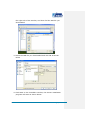
1. Formatting SD Card;
You can download the HP USB Disk Storage Format Tool 2.0.6 from:
http://www.embest-tech.com/resource/download/HP-USB-Disk-S
torage-Format-Tool.rar
And use it to format an SD card; the figure shown below is the tool’s
interface;
Figure 19: Format SD Card
Page | 61
Select FAT32 in the File system drop-down menu, and then click Start to
format the SD card.
Note:
HP USB Disk Storage Format Tool will erase the partitions of SDTF card.
Use other format tool may cause the failure of the TF card booting
2. Updating Image Files;
Copy all the files under X:\linux\image\ to an SD card (where X is the label
of your DVD drive), and then insert it into the SBC8140 and power on the
system; the information on the serial interface is shown below;
Texas Instruments X-Loader 1.47 (Mar 1 2013 - 17:05:22)
Starting X-loader on MMC
Reading boot sector
231872 Bytes Read from MMC
Starting OS Bootloader from MMC...
Starting OS Bootloader...
U-Boot 2010.06-rc1-svn84 (Mar 04 2013 - 12:00:27)
OMAP3630-GP ES2.1, CPU-OPP2 L3-133MHz
OMAP3 SBC8140 board + LPDDR/NAND
I2C:
ready
DRAM: 256 MiB
NAND: 512 MiB
*** Warning - bad CRC or NAND, using default environment
In:
serial
Out:
serial
Err:
serial
Die ID #3d1400029e3800000168682f07003018
Net:
dm9000
Hit any key to stop autoboot: 0
mmc1 is available
reading boot.scr
Page | 62
** Unable to read "boot.scr" from mmc 0:1 **
reading uImage
2548700 bytes read
reading ramdisk.gz
15345565 bytes read
Booting from ramdisk ...
## Booting kernel from Legacy Image at 81000000 ...
Image Name:
Linux-2.6.32
Image Type:
ARM Linux Kernel Image (uncompressed)
Data Size:
2548636 Bytes = 2.4 MiB
Load Address: 80008000
Entry Point:
80008000
Verifying Checksum ... OK
Loading Kernel Image ... OK
OK
Starting kernel ...
Uncompressing
Linux......................................................
...........................................................
............................................. done, booting
the kernel.
Linux version 2.6.32 (tanjian@TIOP) (gcc version 4.4.0 (GCC)
) #5 Sat Mar 2 16:14:46 CST 2013
CPU: ARMv7 Processor [413fc082] revision 2 (ARMv7), cr=10c53c7f
CPU: VIPT nonaliasing data cache, VIPT nonaliasing instruction
cache
Machine: OMAP3 SBC8140 Board
Memory policy: ECC disabled, Data cache writeback
OMAP3630/DM3730 ES1.0 (l2cache iva sgx neon isp 192mhz_clk )
SRAM: Mapped pa 0x40200000 to va 0xfe400000 size: 0x100000
Reserving 12582912 bytes SDRAM for VRAM
Built 1 zonelists in Zone order, mobility grouping on. Total
pages: 65024
Kernel
command
vram=12M
line:
console=ttyS0,115200n8
omapdss.def_disp=lcd
mpurate=1000
omapfb.mode=lcd:4.3inch_LCD
root=/dev/ram0 rw ramdisk_size=65536 initrd=0x81600000,64M
rootfstype=ext2
PID hash table entries: 1024 (order: 0, 4096 bytes)
Page | 63
Dentry cache hash table entries: 32768 (order: 5, 131072 bytes)
Inode-cache hash table entries: 16384 (order: 4, 65536 bytes)
Memory: 256MB = 256MB total
Memory: 176768KB available (4388K code, 378K data, 164K init,
0K highmem)
Hierarchical RCU implementation.
NR_IRQS:402
Clocking rate (Crystal/Core/MPU): 26.0/266/600 MHz
Reprogramming SDRC clock to 266000000 Hz
dpll3_m2_clk rate change failed: -22
GPMC revision 5.0
IRQ: Found an INTC at 0xfa200000 (revision 4.0) with 96
interrupts
Total of 96 interrupts on 1 active controller
OMAP GPIO hardware version 2.5
OMAP clockevent source: GPTIMER12 at 32768 Hz
Console: colour dummy device 80x30
Calibrating delay loop... 480.01 BogoMIPS (lpj=1875968)
Mount-cache hash table entries: 512
CPU: Testing write buffer coherency: ok
regulator: core version 0.5
NET: Registered protocol family 16
Found NAND on CS0
Registering NAND on CS0
Target VDD1 OPP = 4, VDD2 OPP = 2
OMAP DMA hardware revision 5.0
bio: create slab <bio-0> at 0
SCSI subsystem initialized
usbcore: registered new interface driver usbfs
usbcore: registered new interface driver hub
usbcore: registered new device driver usb
i2c_omap i2c_omap.1: bus 1 rev4.0 at 2600 kHz
twl4030: PIH (irq 7) chaining IRQs 368..375
twl4030: power (irq 373) chaining IRQs 376..383
twl4030: gpio (irq 368) chaining IRQs 384..401
regulator: VUSB1V5: 1500 mV normal standby
regulator: VUSB1V8: 1800 mV normal standby
regulator: VUSB3V1: 3100 mV normal standby
twl4030_usb twl4030_usb: Initialized TWL4030 USB module
regulator: VMMC1: 1850 <--> 3150 mV normal standby
regulator: VDAC: 1800 mV normal standby
regulator: VPLL2: 1800 mV normal standby
regulator: VMMC2: 1850 <--> 3150 mV normal standby
Page | 64
regulator: VSIM: 1800 <--> 3000 mV normal standby
i2c_omap i2c_omap.2: bus 2 rev4.0 at 400 kHz
i2c_omap i2c_omap.3: bus 3 rev4.0 at 400 kHz
Switching to clocksource 32k_counter
musb_hdrc:
version
6.0,
musb-dma,
otg
(peripheral+host),
debug=0
musb_hdrc: USB OTG mode controller at fa0ab000 using DMA, IRQ
92
NET: Registered protocol family 2
IP route cache hash table entries: 2048 (order: 1, 8192 bytes)
TCP established hash table entries: 8192 (order: 4, 65536 bytes)
TCP bind hash table entries: 8192 (order: 3, 32768 bytes)
TCP: Hash tables configured (established 8192 bind 8192)
TCP reno registered
UDP hash table entries: 256 (order: 0, 4096 bytes)
UDP-Lite hash table entries: 256 (order: 0, 4096 bytes)
NET: Registered protocol family 1
RPC: Registered udp transport module.
RPC: Registered tcp transport module.
RPC: Registered tcp NFSv4.1 backchannel transport module.
Trying to unpack rootfs image as initramfs...
rootfs image is not initramfs (no cpio magic); looks like an
initrd
Freeing initrd memory: 65536K
omap-iommu omap-iommu.0: isp registered
NetWinder Floating Point Emulator V0.97 (double precision)
ashmem: initialized
VFS: Disk quotas dquot_6.5.2
Dquot-cache hash table entries: 1024 (order 0, 4096 bytes)
msgmni has been set to 473
alg: No test for stdrng (krng)
io scheduler noop registered
io scheduler deadline registered
io scheduler cfq registered (default)
OMAP DSS rev 2.0
OMAP DISPC rev 3.0
OMAP VENC rev 2
Serial: 8250/16550 driver, 4 ports, IRQ sharing enabled
serial8250.0: ttyS0 at MMIO 0x4806a000 (irq = 72) is a ST16654
console [ttyS0] enabled
serial8250.1: ttyS1 at MMIO 0x4806c000 (irq = 73) is a ST16654
serial8250.2: ttyS2 at MMIO 0x49020000 (irq = 74) is a ST16654
serial8250.3: ttyS3 at MMIO 0x49042000 (irq = 80) is a ST16654
Page | 65
brd: module loaded
loop: module loaded
omap2-nand driver initializing
NAND device: Manufacturer ID: 0xad, Chip ID: 0xbc (Hynix NAND
512MiB 1,8V 16-bit)
cmdlinepart partition parsing not available
Creating 5 MTD partitions on "omap2-nand":
0x000000000000-0x000000080000 : "X-Loader"
0x000000080000-0x000000260000 : "U-Boot"
0x000000260000-0x000000280000 : "U-Boot Env"
0x000000280000-0x000000680000 : "Kernel"
0x000000680000-0x000020000000 : "File System"
PPP generic driver version 2.4.2
PPP Deflate Compression module registered
PPP BSD Compression module registered
PPP MPPE Compression module registered
NET: Registered protocol family 24
PPPoL2TP kernel driver, V1.0
dm9000 Ethernet Driver, V1.31
eth0:
dm9000a
at
d0862000,d0866400
IRQ
185
MAC:
00:11:22:33:44:55 (chip)
usbcore: registered new interface driver asix
usbcore: registered new interface driver cdc_ether
usbcore: registered new interface driver cdc_eem
usbcore: registered new interface driver dm9601
usbcore: registered new interface driver smsc95xx
usbcore: registered new interface driver gl620a
usbcore: registered new interface driver net1080
usbcore: registered new interface driver plusb
usbcore: registered new interface driver rndis_host
usbcore: registered new interface driver cdc_subset
usbcore: registered new interface driver zaurus
usbcore: registered new interface driver MOSCHIP usb-ethernet
driver
ehci_hcd: USB 2.0 'Enhanced' Host Controller (EHCI) Driver
ehci-omap ehci-omap.0: OMAP-EHCI Host Controller
ehci-omap ehci-omap.0: new USB bus registered, assigned bus
number 1
ehci-omap ehci-omap.0: irq 77, io mem 0x48064800
ehci-omap ehci-omap.0: USB 2.0 started, EHCI 1.00
hub 1-0:1.0: USB hub found
hub 1-0:1.0: 3 ports detected
Initializing USB Mass Storage driver...
Page | 66
usbcore: registered new interface driver usb-storage
USB Mass Storage support registered.
g_ether gadget: using random self ethernet address
g_ether gadget: using random host ethernet address
usb0: MAC 1e:8b:da:88:c8:d7
usb0: HOST MAC d2:49:09:b6:08:e4
g_ether gadget: Ethernet Gadget, version: Memorial Day 2008
g_ether gadget: g_ether ready
musb_hdrc musb_hdrc: MUSB HDRC host driver
musb_hdrc musb_hdrc: new USB bus registered, assigned bus number
2
hub 2-0:1.0: USB hub found
hub 2-0:1.0: 1 port detected
mice: PS/2 mouse device common for all mice
input: gpio-keys as /devices/platform/gpio-keys/input/input0
input:
TWL4030
Keypad
as
/devices/platform/i2c_omap.1/i2c-1/1-004a/twl4030_keypad/in
put/input1
ads7846 spi1.0: touchscreen, irq 187
input:
ADS7846
Touchscreen
as
/devices/platform/omap2_mcspi.1/spi1.0/input/input2
using rtc device, twl_rtc, for alarms
twl_rtc twl_rtc: rtc core: registered twl_rtc as rtc0
twl_rtc twl_rtc: Power up reset detected.
twl_rtc twl_rtc: Enabling TWL-RTC.
i2c /dev entries driver
ch7033 id:5e
Linux video capture interface: v2.00
tvp514x 2-005d: Registered to v4l2 master omap34xxcam!!
omap-iommu omap-iommu.0: isp: version 1.1
usbcore: registered new interface driver uvcvideo
USB Video Class driver (v0.1.0)
OMAP Watchdog Timer Rev 0x31: initial timeout 60 sec
Registered led device: led0
Registered led device: led1
Registered led device: led2
Registered led device: led3
Registered led device: led4
usbcore: registered new interface driver usbhid
usbhid: USB HID core driver
Advanced Linux Sound Architecture Driver Version 1.0.21.
usb 1-1: new high speed USB device using ehci-omap and address
2
Page | 67
No device for DAI omap-mcbsp-dai-0
No device for DAI omap-mcbsp-dai-1
No device for DAI omap-mcbsp-dai-2
No device for DAI omap-mcbsp-dai-3
No device for DAI omap-mcbsp-dai-4
OMAP3 SBC8140 SoC init
asoc: twl4030 <-> omap-mcbsp-dai-0 mapping ok
ALSA device list:
#0: omap3sbc8140 (twl4030)
TCP cubic registered
NET: Registered protocol family 17
NET: Registered protocol family 15
Power Management for TI OMAP3.
Unable to set L3 frequency (400000000)
Switched to new clocking rate (Crystal/Core/MPU): 26.0/266/1000
MHz
IVA2 clocking rate: 800 MHz
SmartReflex driver initialized
VFP support v0.3: implementor 41 architecture 3 part 30 variant
c rev 3
Console: switching to colour frame buffer device 60x34
regulator_init_complete: incomplete constraints, leaving VDVI
on
regulator_init_complete: incomplete constraints, leaving VDAC
on
hub 1-1:1.0: USB hub found
regulator_init_complete: incomplete constraints, leaving VMMC1
on
hub 1-1:1.0: 4 ports detected
twl_rtc twl_rtc: setting system clock to 2000-01-01 00:00:00
UTC (946684800)
mmc0: host does not support reading read-only switch. assuming
write-enable.
mmc0: new high speed SD card at address 1234
mmcblk0: mmc0:1234 SA02G 1.85 GiB
mmcblk0: p1
tvp514x 2-005d: chip id mismatch msb:0x87 lsb:0x87
tvp514x 2-005d: Unable to detect decoder
tvp514x 2-005d: chip id mismatch msb:0x87 lsb:0x87
tvp514x 2-005d: Unable to detect decoder
tvp514x 2-005d: chip id mismatch msb:0x87 lsb:0x87
tvp514x 2-005d: Unable to detect decoder
tvp514x 2-005d: chip id mismatch msb:0x87 lsb:0x87
Page | 68
tvp514x 2-005d: Unable to detect decoder
omapdss DPI error: display already enabled
omap_vout omap_vout: 'lcd' Display already enabled
omapdss DPI error: display already enabled
omap_vout omap_vout: 'lcd' Display already enabled
omap_vout omap_vout: Buffer Size = 3686400
omap_vout omap_vout: : registered and initialized video device
0
omap_vout omap_vout: Buffer Size = 3686400
omap_vout omap_vout: : registered and initialized video device
1
RAMDISK: gzip image found at block 0
EXT2-fs (ram0): warning: mounting unchecked fs, running e2fsck
is recommended
VFS: Mounted root (ext2 filesystem) on device 1:0.
Freeing init memory: 164K
INIT: version 2.86 booting
Starting udevtar: removing leading '/' from member names
Remounting root file system...
mount: mounting /dev/root on / failed: Invalid argument
mount: mounting /dev/root on / failed: Invalid argument
root: mount: mounting rootfs on / failed: No such file or
directory
root: mount: mounting usbfs on /proc/bus/usb failed: No such
file or directory
Setting up IP spoofing protection: rp_filter.
Configuring network interfaces... udhcpc (v1.11.3) started
Sending discover...
udhcpc: sendto: Network is down
Sending discover...
udhcpc: sendto: Network is down
Sending discover...
udhcpc: sendto: Network is down
No lease, failing
done.
Tue Jan 27 08:47:00 UTC 2009
INIT: Entering runlevel: 5
Starting syslogd/klogd: done
.-------.
|
|
.-.
Page | 69
|
|
|
|
|-----.-----.-----.| |
|
|
|
|
| __
|
|
|---
.----..-----.-----.
---'| '--.| .-'|
||
--'|
|
|
|
'
|
| | | |
'---'---'--'--'--. |-----''----''--' '-----'-'-'-'
-'
|
'---'
The Angstrom Distribution SBC8140 ttyS0
Angstrom 2008.1-test-20090127 SBC8140 ttyS0
SBC8140 login: root (enter root to log in)
The above information indicates that the Linux system has booted up
successfully from the SD card.
Note:
By default the SBC8140 boots from NAND Flash; pressing and holding the
BOOT button before connecting the power can force it to boot from an SD
card.
By default, the system supports a 4.3” screen. If you wish to use another sized
display, please refer to 3.7 Display Mode Configuration to change the display
mode and type boot under the u-boot mode to continue the boot-up process.
3.6.2 Updating System in NAND Flash
Updating image files in NAND Flash requires the help of u-boot. Regardless
of the existence of data in the NAND Flash, image files can be updated by
running u-boot from an SD card.
1. Use the HP USB Disk Storage Format Tool 2.0.6 to format an SD
card to the FAT or FAT32 filesystem;
2. Copy the files MLO, u-boot.bin, x-load.bin.ift_for_NAND,
flash-uboot.bin, uImage and ubi.img from \linux\image of the
DVD-ROM to the SD card;
Page | 70
3. Insert the SD card into the SBC8140 and power it on; when the
information on the serial interface shows a countdown in
seconds, press any key on your PC’s keyboard to enter u-boot
mode;
Texas Instruments X-Loader 1.47 (Mar 1 2013 - 17:05:22)
Starting X-loader on MMC
Reading boot sector
231872 Bytes Read from MMC
Starting OS Bootloader from MMC...
Starting OS Bootloader...
U-Boot 2010.06-rc1-svn84 (Mar 04 2013 - 12:00:27)
OMAP3630-GP ES2.1, CPU-OPP2 L3-133MHz
OMAP3 SBC8140 board + LPDDR/NAND
I2C:
ready
DRAM: 256 MiB
NAND: 512 MiB
*** Warning - bad CRC or NAND, using default environment
In:
serial
Out:
serial
Err:
serial
Die ID #3d1400029e3800000168682f07003018
Net:
dm9000
Hit any key to stop autoboot: 0 (press any key to enter u-boot
mode)
4. Type run updatesys and press the Enter key to start a system
update; the information on the serial interface is shown below;
OMAP3 SBC8140 # run updatesys
NAND erase: device 0 whole chip
Erasing at 0x1ffe0000 -- 100% complete.
OK
mmc1 is available
reading x-load.bin.ift_for_NAND
Page | 71
11648 bytes read
HW ECC selected
NAND write: device 0 offset 0x0, size 0x2d80
12288 bytes written: OK
reading flash-uboot.bin
231872 bytes read
SW ECC selected
NAND write: device 0 offset 0x80000, size 0x389c0
233472 bytes written: OK
reading uImage
2548700 bytes read
SW ECC selected
NAND write: device 0 offset 0x280000, size 0x26e3dc
2549760 bytes written: OK
reading ubi.img
12320768 bytes read
SW ECC selected
NAND write: device 0 offset 0x680000, size 0xbc0000
12320768 bytes written: OK
When the LEDs on the kit start to blink, the update is completed; please
remove the SD card and reboot the system;
3.7 Display Mode Configuration
The system supports multiple display modes. Users can select an
appropriate mode by configuring boot parameters. The following contents
show how to configure for both 4.3” and 7” LCDs, VGA mode and LVDS
mode.
You need to enter u-boot mode to complete these configurations. Please
reboot the kit and press any key on your PC’s keyboard when the system
prompts you with a countdown in seconds as shown below;
Page | 72
Texas Instruments X-Loader 1.47 (Mar 1 2013 - 17:05:22)
Starting X-loader on MMC
Reading boot sector
231872 Bytes Read from MMC
Starting OS Bootloader from MMC...
Starting OS Bootloader...
U-Boot 2010.06-rc1-svn84 (Mar 04 2013 - 12:00:27)
OMAP3630-GP ES2.1, CPU-OPP2 L3-133MHz
OMAP3 SBC8140 board + LPDDR/NAND
I2C:
ready
DRAM: 256 MiB
NAND: 512 MiB
*** Warning - bad CRC or NAND, using default environment
In:
serial
Out:
serial
Err:
serial
Die ID #3d1400029e3800000168682f07003018
Net:
dm9000
Hit any key to stop autoboot: 0
(press any key to enter u-boot mode)
1. Configuring for a 4.3” LCD;
Execute the following instructions in u-boot mode to configure for 4.3”
display mode;
OMAP3 SBC8140 # setenv defaultdisplay lcd
OMAP3 SBC8140 # setenv dispmode 4.3inch_LCD
OMAP3 SBC8140 # saveenv
2. Configuring for a 7” LCD;
Execute the following instructions in u-boot mode to configure for 7”
display mode;
OMAP3 SBC8140 # setenv defaultdisplay lcd
OMAP3 SBC8140 # setenv dispmode 7inch_LCD
OMAP3 SBC8140 # saveenv
Page | 73
3. Configuring for VGA;
Execute the following instructions in u-boot mode to configure for VGA
display mode;
OMAP3 SBC8140 # setenv defaultdisplay lcd
OMAP3 SBC8140 # setenv dispmode VGA
OMAP3 SBC8140 # saveenv
4. Configuring for LVDS;
Execute the following instructions in u-boot mode to configure for LVDS
display mode;
OMAP3 SBC8140 # setenv defaultdisplay lcd
OMAP3 SBC8140 # setenv dispmode LVDS
OMAP3 SBC8140 # saveenv
3.8 Tests and Demonstrations
This section will carry out many tests on the SBC8140s devices and also
demonstrations of the Android and DVSDK systems.
Note:
The following tests are all implemented by entering instructions in a
HyperTerminal window.
3.8.1 Testing LEDs
1. Execute the following instructions to test LED0;
root@SBC8140:# echo 1 > /sys/class/leds/led0/brightness
root@SBC8140:# echo 0 > /sys/class/leds/led0/brightness
2. Execute the following instructions to test LED1;
root@SBC8140:# echo 1 > /sys/class/leds/led1/brightness
root@SBC8140:# echo 0 > /sys/class/leds/led1/brightness
3. Execute the following instructions to test LED2;
root@SBC8140:# echo 1 > /sys/class/leds/led2/brightness
Page | 74
root@SBC8140:# echo 0 > /sys/class/leds/led2/brightness
4. Execute the following instructions to test LED3;
root@SBC8140:# echo 1 > /sys/class/leds/led3/brightness
root@SBC8140:# echo 0 > /sys/class/leds/led3/brightness
When executing each instruction, the corresponding LED will be turned on
or turned off.
3.8.2 Testing a Touch-Screen
Boot up the SBC8140 from NAND Flash and start testing;
1. Execute the following instruction to calibrate the touch-screen;
root@SBC8140: # ts_calibrate
Touch all the “+” marks on the screen by following the screen prompt
information to finish calibration;
2. Execute the following instruction to test the touch-screen;
root@SBC8140: # ts_test
Draw points and lines on the screen as you see the prompt information to
proceed with testing;
3.8.3 Testing the RTC
The SBC8140 has a hardware clock which can store and recover the
system clock; please carry out testing of the RTC through the following
steps;
1. Execute the following instruction to set system clock to 8 pm,
Aug. 8th, 2011;
root@SBC8140 : # date 080820002011
The information in HyperTerminal window is shown below;
Mon Aug 8 20:00:00 UTC 2011
2. Execute the following instruction to write the system clock into
RTC;
root@SBC8140: # hwclock -w
3. Execute the following instruction to read the RTC;
Page | 75
root@SBC8140: # hwclock
The information in HyperTerminal window is shown below;
Mon Aug 8 20:01:01 2011 0.000000 seconds
The above information indicates that system clock has been stored in the
hardware clock;
4. Reboot the system and execute the following instructions to
recover the system clock;
root@SBC8140: # hwclock -s
root@SBC8140: # date
The information in the HyperTerminal window is shown below;
Mon Aug 8 20:01:01 2011 0.000000 seconds
The above information indicates that the system clock has been recovered
with the hardware clock;
Note:
SBC8140 is not provided with a CR2032 battery by default, this must be
purchased separately.
3.8.4 Testing an SD Card
1. Insert an SD card into the SBC8140, the system will mount it
under /media/ automatically; please execute the following
instructions to view the name of the SD device in the system;
root@SBC8140:~# cd /media/
root@SBC8140:/media# ls
The information in the HyperTerminal window is shown below;
card
hdd
mmcblk0p1 ram
cf
mmc1
net
union
realroot
Page | 76
2. Execute the following instruction to view the contents of the SD
card;
root@SBC8140:/media# ls mmcblk0p1/
The information in the HyperTerminal window is shown below;
flash-uboot.bin
u-boot.bin
mlo
x-load.bin.ift_for_NAND
uImage
ramdisk.gz
ubi.img
3.8.5 Testing a USB Device
Testing of a USB device is accomplished by creating a network
communication between the miniUSB interface on the kit and a USB
interface on the PC;
1. After the system boots up, connect the SBC8140 to your PC
with a Mini B-to-USB A cable, then install the Linux USB
Ethernet driver; please refer to Appendix 2:Driver Installation
Of Linux USB Ethernet/RNDIS GadgetError! Reference
source not found..
2. Execute the following instructions to set the IP addresses of the
SBC8140 (the IP used below is only for reference; you can
select a different IP as required);
root@SBC8140:~#
ifconfig usb0 192.168.1.115
root@SBC8140:~#
ifconfig
The information in the HyperTerminal window is shown below;
lo
Link encap:Local Loopback
inet addr:127.0.0.1 Mask:255.0.0.0
UP LOOPBACK RUNNING MTU:16436
Metric:1
RX packets:26 errors:0 dropped:0 overruns:0 frame:0
TX packets:26 errors:0 dropped:0 overruns:0 carrier:0
collisions:0 txqueuelen:0
RX bytes:2316 (2.2 KiB) TX bytes:2316 (2.2 KiB)
usb0
Link encap:Ethernet HWaddr 5E:C5:F6:D4:2B:91
inet
addr:192.168.1.115
Bcast:192.168.1.255
Mask:255.255.255.0
Page | 77
UP BROADCAST RUNNING MULTICAST MTU:1500 Metric:1
RX packets:253 errors:0 dropped:0 overruns:0 frame:0
TX packets:43 errors:0 dropped:0 overruns:0 carrier:0
collisions:0 txqueuelen:1000
RX bytes:35277 (34.4 KiB) TX bytes:10152 (9.9 KiB)
3. Right-click My Network Places on the desktop of your PC and
select Properties to open the Network Connections
window; you can find a new Local Area Connection in the
window;
4. Right-click the icon of the new Local Area Connection and
select Properties, and then double-click Internet Protocol
(TCP/IP) to open the following window;
Figure 20: Setting IP Address
Set the IP address of the USB virtual network interface as the same
network segment as that SBC8140’s IP was set in, and then click OK;
Page | 78
5. Use a ping command in the HyperTerminal window to test if the
network works properly;
root@SBC8140:~# ping 192.168.1.15
The information in the HyperTerminal window is shown below;
PING 192.168.1.15 (192.168.1.15): 56 data bytes
64 bytes from 192.168.1.15: seq=0 ttl=128 time=0.885 ms
64 bytes from 192.168.1.15: seq=1 ttl=128 time=0.550 ms
The
above
information
indicates
the
network
has
been
created
successfully.
3.8.6 Testing USB HOST
1. Insert a flash disk into the USB interface on the SBC8140, the
system will display the following information;
root@SBC8140:/# usb 1-1.4: new high speed USB device using
ehci-omap and address 3
scsi0 : usb-storage 1-1.4:1.0
scsi 0:0:0:0: Direct-Access
SanDisk
Flash Memory
0.1
PQ: 0 ANSI: 2
sd 0:0:0:0: [sda] 2001888 512-byte logical blocks: (1.02 GB/977
MiB)
sd 0:0:0:0: [sda] Write Protect is off
sd 0:0:0:0: [sda] Assuming drive cache: write through
sd 0:0:0:0: [sda] Assuming drive cache: write through
sda: sda1
sd 0:0:0:0: [sda] Assuming drive cache: write through
sd 0:0:0:0: [sda] Attached SCSI removable disk
2. The system will mount the flash disk under /media/
automatically; please execute the following instructions to view
the contents of the disk;
root@SBC8140:/media# ls /media/sda1/
The information in the HyperTerminal window is shown below;
flash-uboot.bin
mlo
ramdisk.gz
u-boot.bin
x-load.bin.ift_for_NAND
uImage
ubi.img
Page | 79
3.8.7 Testing the Audio Function
The SBC8140 has input/output interfaces which support audio recording
and playback. The filesystem is integrated with the alsa-utils audio
recording and playback tool. You can test it by following the steps below
;
1. Insert a microphone into the 3.5mm audio input interface (the
green one) on the SBC8140, and then execute the following
instruction to start audio recording;
root@SBC8140:~# arecord -t wav -c 1 -r 44100 -f S16_LE -v k
The information in the HyperTerminal window is shown below;
Recording WAVE 'k' : Signed 16 bit Little Endian, Rate 44100
Hz, Stereo
Plug PCM: Hardware PCM card 0 'omap3evm' device 0 subdevice 0
Its setup is:
stream
: CAPTURE
access
: RW_INTERLEAVED
format
: S16_LE
subformat
: STD
channels
: 2
rate
exact rate
msbits
: 44100
: 44100 (44100/1)
: 16
buffer_size
: 22052
period_size
: 5513
period_time
: 125011
tstamp_mode
: NONE
period_step
: 1
avail_min
: 5513
period_event : 0
start_threshold
: 1
stop_threshold
: 22052
silence_threshold: 0
silence_size : 0
boundary
: 1445199872
appl_ptr
: 0
hw_ptr
: 0
Page | 80
2. Insert an earphone into the 3.5mm audio output interface (the
red one), and then execute the following instruction to play the
recorded audio;
root@SBC8140:~# aplay -t wav -c 2 -r 44100 -f S16_LE -v k
The information in the HyperTerminal window is shown below;
Playing WAVE 'k' : Signed 16 bit Little Endian, Rate 44100 Hz,
Stereo
Plug PCM: Hardware PCM card 0 'omap3evm' device 0 subdevice 0
Its setup is:
stream
: PLAYBACK
access
: RW_INTERLEAVED
format
: S16_LE
subformat
: STD
channels
: 2
rate
: 44100
exact rate
msbits
: 44100 (44100/1)
: 16
buffer_size
: 22052
period_size
: 5513
period_time
: 125011
tstamp_mode
: NONE
period_step
: 1
avail_min
: 5513
period_event : 0
start_threshold
stop_threshold
: 22052
: 22052
silence_threshold: 0
silence_size : 0
boundary
: 1445199872
appl_ptr
: 0
hw_ptr
: 0
3.8.8 Testing the Network Connection
1. Set the IP address of the SBC8140 to the same network
segment as that of your PC, for example, execute the following
instructions;
root@SBC8140:~# ifconfig eth0 192.192.192.203
root@SBC8140:~# ifconfig
Page | 81
The information in the HyperTerminal window is shown below;
eth0
Link encap:Ethernet HWaddr 00:11:22:33:44:55
inet
addr:192.192.192.203
Bcast:192.192.192.255
Mask:255.255.255.0
UP BROADCAST MULTICAST MTU:1500
Metric:1
RX packets:0 errors:0 dropped:0 overruns:0 frame:0
TX packets:0 errors:0 dropped:0 overruns:0 carrier:0
collisions:0 txqueuelen:1000
RX bytes:0 (0.0 B) TX bytes:0 (0.0 B)
Interrupt:185 Base address:0x2000
2. Execute the following instruction to test the
communication between the SBC8140 and the PC;
network
root@SBC8140:~# ping 192.192.192.170
The information in the HyperTerminal window is shown below;
Table 1-1
Testing Network
PING 192.192.192.170 (192.192.192.170): 56 data bytes
64 bytes from 192.192.192.170: seq=0 ttl=128 time=4.486 ms
64 bytes from 192.192.192.170: seq=1 ttl=128 time=0.336 ms
The above information indicates the network is working properly.
3.8.9 Testing the CameraCam8000-A
Connect the camera module (needs to be purchased separately), CCD
camera and LCD screen to the SBC8140, and then execute the following
instructions;
root@SBC8140:~# saMmapLoopback
The information in the HyperTerminal window is shown below;
tvp514x 2-005d: tvp5146m2 found at 0xba (OMAP I2C adapter)
Capture: Opened Channel
Capture: Current Input: COMPOSITE
Capture: Current standard: PAL
Capture: Capable of streaming
Page | 82
Capture: Number of requested buffers = 3
Capture: Init done successfully
Display: Opened Channel
Display: Capable of streaming
Display: Number of requested buffers = 3
Display: Init done successfully
Display: Stream on...
Capture: Stream on...
The images captured by the CCD camera can be seen on the LCD screen.
3.8.10 Testing the CDMA8000-U Module
Please download the user manual for the module from:
http://www.timll.com/chinese/uploadFile/cdma8000.rar
And follow the instructions in the manual to complete the test.
Note:
CDMA8000-U is an optional module. It must be purchased separately.
3.8.11 Testing the WCDMA8000-U Module
Please download the user manual for the module from:
http://www.timll.com/chinese/uploadFile/WCDMA8000.zip
And follow the instructions in the manual to complete the test.
Page | 83
Notice:
WCDMA8000-U is an optional module. It must be purchased
separately.
3.8.12 Demonstration of the Android System
Copy all the files under X:\linux\demo\Android\image (where X is the label
of your DVD drive) to an SD card and insert it into the SBC8140, then
power on the kit while pressing and holding the BOOT button (Button
CN121); The information in the HyperTerminal window is shown below;
60
Texas Instruments X-Loader 1.47 (Apr 23 2012 - 09:09:16)
Starting X-loader on MMC
Reading boot sector
1154092 Bytes Read from MMC
Starting OS Bootloader from MMC...
Starting OS Bootloader...
U-Boot 2010.06-rc1-svn (Apr 17 2012 - 10:28:23)
OMAP34xx/35xx-GP ES2.1, CPU-OPP2 L3-165MHz
OMAP3 SBC8140 board + LPDDR/NAND
I2C:
ready
DRAM: 256 MiB
NAND: 512 MiB
*** Warning - bad CRC or NAND, using default environment
In:
serial
Out:
serial
Err:
serial
SBC8140 xM Rev A
Die ID #259000029e38000001683b060d023028
NAND erase: device 0 whole chip
Skipping bad block at
0x08660000
Erasing at 0x1ffe0000 -- 100% complete.
OK
Page | 84
mmc1 is available
reading x-load.bin.ift_for_NAND
11668 bytes read
HW ECC selected
NAND write: device 0 offset 0x0, size 0x2d94
12288 bytes written: OK
reading flash-uboot.bin
1152640 bytes read
SW ECC selected
NAND write: device 0 offset 0x80000, size 0x119680
1153024 bytes written: OK
reading uImage
2573772 bytes read
SW ECC selected
NAND write: device 0 offset 0x280000, size 0x2745cc
2574336 bytes written: OK
reading ubi.img
79036416 bytes read
SW ECC selected
NAND write: device 0 offset 0x680000, size 0x4b60000
79036416 bytes written: OK
When the LEDs on the kit start to blink, the programming process is
completed; please remove the SD card and reboot the kit to enter the
Android operating system.
Note:
By default, the system supports a 4.3” screen. If you require another display
size, please refer to 3.7 Display Mode Configuration.
Page | 85
3.8.13 Demonstration of the DVSDK System
The DVSDK (Digital Video Software Development Kit) is software released
by TI to build connections between ARM processors and DSPs.
Applications are running on the ARM end which process IO interfaces and
applications. ARM uses VISA APIs interface provided by the Codec Engine
to process videos, images and audio signals; and then the Codec Engine
communicates with the Codec Engine server created by DSP using a
DSP/BIOS Link as well as xDIAS and xDM protocols. The DSP will process
these signals and put the results in a memory space shared with ARM,
allowing access to the results from the ARM end.
Format an SD card as two partitions (please refer to Appendix
3:Making a Linux Boot Disk
1. Making a Linux Boot Disk) and connect it to your PC with a SD
card reader, then execute the following instructions in an
Ubuntu Linux system;
cp /media/cdrom/linux/demo/dvsdk/image/MLO /media/LABEL1
cp /media/cdrom/linux/demo/dvsdk/image/u-boot.bin /media/LABEL1
cp /media/cdrom/linux/demo/dvsdk/image/uImage /media/LABEL1/uImage
rm -rf /media/LABEL2/*
sudo
tar
xvf
/media/cdrom/linux/demo/dvsdk/image/dvsdk-dm37x-evm-rootfs.tar.bz2 -C
/media/LABEL2
sync
umount /media/LABEL1
umount /media/LABEL2
2. Insert the SD card into the SBC8140, then power on the kit
while pressing and holding the BOOT button(Button CN12)and
power on the kit; the information in the HyperTerminal window
is shown below;
2548012 bytes read
## Booting kernel from Legacy Image at 80300000 ...
Image Name:
Linux-2.6.32
Image Type:
ARM Linux Kernel Image (uncompressed)
Data Size:
2547948 Bytes = 2.4 MiB
Page | 86
Load Address: 80008000
Entry Point:
80008000
Verifying Checksum ... OK
Loading Kernel Image ... OK
OK
Starting kernel ...
//Middle section is omitted 中间部分省略
……
Formatted: Font: (Default) Courier
New, Bold
Arago Project http://arago-project.org dm37x-evm ttyS2
Arago 2010.07 dm37x-evm ttyS2
dm37x-evm login:root
(enter root here to log in)
Enter the user name root to log in the system when you see prompt
information dm37x-evm login in the HyperTerminal window;
3. The filesystem of the DVSDK has been pre-installed some
applications; the following contents will take GStreamer
pipelines as the example to demonstrate H.264 decoding;
please execute the following instructions;
root@dm37x-evm:cd /usr/share/ti/gst/omap3530
root@dm37x-evm:/usr/share/ti/gst/omap3530#
./loadmodules.sh
root@dm37x-evm:/usr/share/ti/gst/omap3530#
gst-launch
filesrc
location=/usr/share/ti/data/videos/davincieffect_480p30.264
\!
typefind ! TIViddec2 ! TIDmaiVideoSink -v
The information in the HyperTerminal window is shown below;
Setting pipeline to PAUSED ...
/GstPipeline:pipeline0/GstTypeFindElement:typefindelement0.
GstPad:src: caps = video/x-h264
Pipeline is PREROLLING ...
/GstPipeline:pipeline0/GstTIViddec2:tividdec20.GstPad:sink:
caps = video/x-h264
/GstPipeline:pipeline0/GstTIViddec2:tividdec20.GstPad:src:
caps
=
video/x-raw-yuv,
framerate=(fraction)30000/1001,
format=(fourcc)UYVY,
width=(int)720,
height=(int)576
/GstPipeline:pipeline0/GstTIViddec2:tividdec20.GstPad:src:
caps
=
video/x-raw-yuv,
framerate=(fraction)30000/1001,
format=(fourcc)UYVY,
width=(int)720,
Page | 87
height=(int)480
/GstPipeline:pipeline0/GstTIDmaiVideoSink:tidmaivideosink0.
GstPad:sink:
caps
=
video/x-raw-yuv,
format=(fourcc)UYVY,
framerate=(fraction)30000/1001,
width=(int)720,
height=(int)480
Pipeline is PREROLLED ...
Setting pipeline to PLAYING ...
New clock: GstSystemClock
A video clip will be played on the LCD screen.
Note:
For
the
details
of
DVSDK,
please
visit
TI’s
website
or
TMS320DM3730_Software_Developers_Guide.pdf
view
under
X:\linux\demo\dvsdk\source\ (where X is the label of your DVD drive).
By default, the system supports a 4.3” screen. If you require another display
size, please refer to 3.7 Display Mode Configuration.
3.9 Development of Applications
This section will introduce the common process of application development
through an LED example application.
1. Compose the source code led_acc.c to instruct the three LEDs
on the SBC8140 to blink in the mode of an accumulator;
#include <stdio.h>
#include <unistd.h>
#include <sys/types.h>
#include <sys/ipc.h>
#include <sys/ioctl.h>
#include <fcntl.h>
#define LED1 “/sys/class/leds/led1/brightness”
#define LED2 “/sys/class/leds/led2/brightness”
#define LED3 “/sys/class/leds/led3/brightness”
Page | 88
int main(int argc, char *argv[])
{
int f_led1, f_led2, f_led3;
unsigned char i = 0;
unsigned char dat1, dat2, dat3;
if((f_led1 = open(LED1, O_RDWR)) < 0){
printf(“error in open %s”,LED1);
return -1;
}
if((f_led2 = open(LED2, O_RDWR)) < 0){
printf(“error in open %s”,LED2);
return -1;
}
if((f_led3 = open(LED3, O_RDWR)) < 0){
printf(“error in open %s”,LED3);
return -1;
}
for(;;){
i++;
dat1 = i&0x1 ? ‘1’:’0’;
dat2 = (i&0x2)>>1 ? ‘1’:’0’;
dat3 = (i&0x4)>>2 ? ‘1’:’0’;
write(f_led1, &dat1, sizeof(dat1));
write(f_led2, &dat2, sizeof(dat2));
write(f_led3, &dat3, sizeof(dat3));
usleep(300000);
}
}
2. Execute the following instruction in an Ubuntu Linux system to
implement cross compilation;
arm-none-linux-gnueabi-gcc led_acc.c -o led_acc
3. Download the compiled files to the SBC8140 and enter the
directory where the file led_acc is saved, then execute the
following instruction to run the LED application;
./led_acc &
Page | 89
4 WinCE Operating System
This chapter will mainly cover system and application development based
on the SBC8140 under Windows Embedded CE 6.0 R3, as well as the
software resources and features on the DVD-ROM, building a development
environment, and how to compile projects and the BSP (Board Support
Package).
4.1 Software Resources
The DVD-ROM provided along with the kit contains an abundance of
software resources; the following tables will help find them in the
DVD-ROM (where X is the label of your DVD drive).
X:\WINCE600\bsp\mini8510.rar
X:\WINCE600\bsp\COMMON_TI_V1.rar
BSP
X:\WINCE600\bsp\dvsdk_wince_01_11_00_02.rar
X:\WINCE600\SGX\wince_gfx_sgx_01_01_00_patch_01_setup.exe
Example
Project
Example
Application
X:\WINCE600\prj\mini8510.rar
X:\WINCE600\app\GPIOAppDemo.rar
X:\WINCE600\image\
Pre-Compil
MLO
First bootloader for SD card boot
XLDRNAND.nb0
First bootloader for NAND boot
EBOOTSD.nb0
Second bootloader for SD card boot
EBOOTNAND.nb0
Second bootloader for NAND boot
NK.bin
WinCE runtime image
ed Image
files
Page | 90
4.2 BSP Package Contents
Categories
X-Loader
(First-Level
Boot Code)
EBOOT
(Second-Level
Boot Code)
OAL
Drivers
Codes
Code Types
NAND
Source Code
NOR
Source Code
SD
Source Code
NAND
Source Code
NOR
Source Code
SD
Source Code
KILT(USB RNDIS)
Source Code
REBOOT
Source Code
Watchdog
Source Code
RTC
Source Code
System timer
Source Code
Interrupt controller
Source Code
Low power suspend
Source Code
NLED driver
Source Code
GPIO/I2C/SPI/MCBSP driver
Source Code
Series port driver
Source Code
6X6 keyboard driver
Source Code
Audio driver
Source Code
NAND driver
Source Code
Display
driver
(LCD/DVI/VGA/S-Video/Composite
Source Code
Video)/ TOUCH driver
SD/MMC/SDIO driver
Source Code
Page | 91
Categories
Codes
DM9000 network card driver
Source Code
USB OTG driver
Source Code
USB EHCI driver
Source Code
VRFB driver
Source Code
DSPLINKK/CMEMK driver
Binary Code
AAC/MPEG2/MPEG4/H264
Hardware decode filter
SDK
Code Types
DSP
Binary Code
GPIO keyboard driver
Source Code
PWM(TPS65930) driver
Source Code
ADC(TPS65930) driver
Source Code
ONENAND driver
Source Code
Analogue Camera driver
Source Code
Digital Camera driver
Source Code
DMA driver
Source Code
RTC driver
Source Code
Backlight driver
Source Code
Battery driver
Source Code
Sleep / wakeup button driver
Source Code
DVFS/Smart Reflex
Source Code
powerVR DDK & SDK
Binary Code &
Source Code
Page | 92
4.3 Process of System Development
This section will walk you through the system development process by
introducing
the
installation
of
an
IDE
(integrated
development
environment), uncompressing/copying of the BSP and example projects,
and the compilation of a first-level sysgen and the BSP.
4.3.1 Installing the IDE
To build a WinCE IDE, a series of software (as listed in the following table)
needs to be installed under Windows XP or Vista; please make sure they
are installed in the order specified in the table below so as to avoid
unexpected errors.
No.
Software
1
Visual Studio 2005
2
Visual Studio 2005 SP1
3
Visual Studio 2005 SP1 Update for Vista (vista system require)
4
Windows Embedded CE 6.0 Platform Builder
5
Windows Embedded CE 6.0 SP1
6
Windows Embedded CE 6.0 R2
7
Windows Embedded CE 6.0 Product Update Rollup 12/31/2008
8
Windows Embedded CE 6.0 R3
9
Windows Embedded CE 6.0 Product Update Rollup 12/31/2009
10
ActiveSync 4.5
11
Windows Mobile 6 Professional SDK
4.3.2 Uncompressing/Copying the BSP and Example Projects
Please follow the information in the table below to uncompress/copy the
BSP and example projects from the DVD-ROM to a specified location on the
PC.
Page | 93
Operation
Uncompress
Uncompress
Uncompress
Source Address
Destination Address
X:\WNCE600\bsp\mini8510.
rar
X:\WINCE600\bsp\COMMON
C:\WINCE600\PLATFORM\COMMON\
_TI_V1.rar
SRC\SOC
X:\WINCE600\bsp\dvsdk_wi
nce_01_11_00_02.rar
X:\WINCE600\SGX\wince_gf
x_sgx_01_01_00_patch_01
Install
_setup.exe
C:\TI\wince_gfx_sgx_01_01
Copy
_00_patch_01\poweVR
Copy
C:\WINCE600\PLATFORM
X:\WINCE600\prj\mini8510
C:\WINCE600\3rdParty\
C:\TI\wince_gfx_sgx_01_01_00_pat
ch_01
C:\WINCE600\public
C:\WINCE600\OSDesigns
Note:
The default installation path of Windows Embedded CE 6.0 is C:\WINCE600 in
this document.
4.3.3 Compiling Sysgen and the BSP
Please follow the steps listed below to complete compilation of sysgen and
the BSP.
1. Open
the
project
file
mini8510.sln
located
under
C:\WINCE600\OSDesigns\mini8510;
2. Select Build > Build Solution on the main bar of the Visual
Studio 2005 window to start compiling sysgen and the BSP;
3. After compilation is done, copy the images MLO, EBOOTSD.nb0
and
NK
from
C:\WINCE600\OSDesigns\mini8510\mini8510\RelDir\mini85
Page | 94
10_ARMV4I_Release to an SD card and insert it into the
SBC8140, then power on the kit;
4. Press the Space key on your PC’s keyboard to enter the eboot
menu and type a to select a proper graphic output, and then
type the number 0 to boot the system;
4.4 Introduction to Drivers
The figure shown below illustrates the architecture of the BSP for the
SBC8140;
Figure 21: BSP Architecture
The following table lists the paths of all the driver source code in the BSP;
Driver Names
NLED driver
Paths
bsp\mini8510\SRC\DRIVERS\NLED
bsp\mini8510\SRC\DRIVERS\GPIO
GPIO
bsp\COMMON_TI_V1\COMMON_TI\GPIO
bsp\COMMON_TI_V1\COMMON_TI\OAL\OMAP_OALI2C
I2C
bsp\COMMON_TI_V1\COMMON_TI\CEDDK\I2C
Page | 95
Driver Names
Paths
SPI
bsp\COMMON_TI_V1\COMMON_TI\SPI
bsp\COMMON_TI_V1\COMMON_TI\MCBSP
MCBSP driver
bsp\COMMON_TI_V1\OMAP3530\MCBSP
Series port driver
bsp\COMMON_TI_V1\COMMON_TI\SERIAL
bsp\COMMON_TI_V1\COMMON_TI\KEYPAD
6X6 keyboard driver
bsp\mini8510\SRC\DRIVERS\TPS659XX_KEYPAD
bsp\mini8510\SRC\DRIVERS\TPS659XX_WAVE
Audio driver
bsp\COMMON_TI_V1\TPS659XX\WAVE
bsp\OMAP35XX_TPS659XX_TI_V1\omap35xx\BLOCK
NAND driver
bsp\COMMON_TI_V1\COMMON_TI\BLOCK
bsp\COMMON_TI_V1\COMMON_TI\DSS
Display driver ( LCD/DVI. S
-Video/Composite Video)
bsp\mini8510\SRC\BSP_COMMON\DISPLAY
bsp\mini8510\SRC\DRIVERS\DISPLAY
TOUCH driver
bsp\mini8510\SRC\DRIVERS\TOUCH
bsp\mini8510\SRC\DRIVERS\SDBUS
bsp\mini8510\SRC\DRIVERS\SDHC
SD/MMC/SDIO driver
bsp\mini8510\SRC\DRIVERS\SDMEMORY
bsp\COMMON_TI_V1\COMMON_TI\SDHC
SMSC9514
network
driver
card
bsp\mini8510\SRC\DRIVERS\SMSC9514
bsp\mini8510\SRC\DRIVERS\MUSB
USB OTG driver
bsp\COMMON_TI_V1\OMAP3530\MUSB
bsp\COMMON_TI_V1\TPS659XX\USBOTG
bsp\ COMMON_TI_V1\COMMON_TI\USB
USB EHCI driver
bsp\ COMMON_TI_V1\OMAP3530\USB
Page | 96
Driver Names
Paths
mini8510\SRC\DRIVERS\USBHS
VRFB driver
bsp\ COMMON_TI_V1\COMMON_TI\VRFB
DSPLINKK/CMEMK
bsp\3rdParty\dvsdk_wince_01_11_00_02
AAC/MPEG2/MPEG4/H264
DSP hardware decode filter
bsp\3rdParty\dvsdk_wince_01_11_00_02
bsp\COMMON_TI_V1\COMMON_TI\KEYPAD
GPIO keyboard driver
bsp\mini8510\SRC\DRIVERS\TPS659XX_KEYPAD
PWM(TPS65930)driver
bsp\ COMMON_TI_V1\TPS659XX\TLED
ADC(TPS65930)driver
bsp\ COMMON_TI_V1\TPS659XX\MADC
bsp\mini8510\SRC\DRIVERS\CAMERA
Camera driver
bsp\mini8510\SRC\DRIVERS\CAMERA_Digital
Backlight driver
bsp\mini8510\SRC\DRIVERS\BACKLIGHT
Battery driver
bsp\mini8510\SRC\DRIVERS\BATTERY
bsp\mini8510\SRC\DRIVERS\TPS659XX_PWRKEY (known
Sleep/wake-up button driver
issue: system cannot be woken up from suspending mode
when tps65930 otg is involved)
bsp\ COMMON_TI_V1\COMMON_TI\PM
DVFS/Smart Reflex
bsp\ mini8510\SRC\DRIVERS\PM
DMA driver
bsp\ COMMON_TI_V1\COMMON_TI\SDMA
bsp\ COMMON_TI_V1\TPS659XX\OALRTC
RTC driver
bsp\mini8510\SRC\DRIVERS\TPS659XX_RTC
Page | 97
If you need more examples of the development of WinCE drivers, please
select:
Start
All Programs
Microsoft Visual Studio 2005
Microsoft Visual Studio Document
Content(C)
Windows Embedded CE 6.0
Develop a Device Driver
From your PC’s desktop.
4.5 System Update
This section will show you how to update the WinCE system in an SD card
and NAND Flash.
4.5.1 Updating the System in an SD Card
You can download the HP USB Disk Storage Format Tool 2.0.6 from:
http://www.embest-tech.com/resource/download/HP-USB-Disk-S
torage-Format-Tool.rar.
http://www.embedinfo.com/english/download/SP27213.exe
And use it to format an SD card; the figure shown below is the tool’s
interface;
Page | 98
Formatted: Font: Bold
Formatted: Normal
Figure 22: Format SD Card
1. Select FAT32 in the File system drop-down menu, and then
click Start to format the SD card.
2. Copy the files MLO, EBOOTSD.nb0 and NK.bin from
X:\WINCE600\image\ (where X is the label of your DVD drive)
to the SD card;
Notice:
HP USB Disk Storage Format Tool will erase the partitions of TF card.
Use other format tool may cause the failure of the TF card bootingIf partitions
need to be retained, please use the format function of Windows system.
Page | 99
3. Insert the SD card into the SBC8140 and power it on while
pressing and holding the BOOT button (Button CN121); the
information in the HyperTerminal window is shown below;
60
Texas Instruments Windows CE SD X-Loader for EVM 3730
Built May 29 2012 at 14:43:06
Version BSP_WINCE_ARM_A8 1.01.00.03
open ebootsd.nb0 file
Init HW: controller RST
SDCARD: requested speed 1000000, actual speed 1000000
SDCARD: requested speed 25000000, actual speed 19200000
jumping to ebootsd image
Microsoft Windows CE Bootloader Common Library Version 1.4 Built
May 29 2012 14:39:28
Texas Instruments Windows CE EBOOT for OMAP35xx/37xx, Built May
29 2012 at 15:19:04
EBOOT Version 0.0, BSP BSP_WINCE_ARM_A8 1.01.00.03
TI OMAP3730 Version 0x00000012 (ES1.2)
TPS659XX Version 0x30 (ES1.3)
System ready!
Preparing for download...
INFO: Predownload....
Checking bootloader blocks are marked as reserved (Num = 14)
Skip bad block 4
Skip bad block 5
Skip bad block 6
Skip bad block 8
Skip bad block 11
WARN: Boot config wasn't found, using defaults
INFO: SW4 boot setting: 0x2f
>>> Forcing cold boot (non-persistent registry and other data
will be wiped) <<<
Hit space to enter configuration menu 5... (press Space key to
enter eboot menu)
Page | 100
4. When you see the HyperTerminal information counting down in
seconds, please press the Space key on your PC’s keyboard to
enter the eboot menu.
5. Type a in the following eboot menu;
------------------------------------------------------------------------------Main Menu
------------------------------------------------------------------------------[1] Show Current Settings
[2] Select Boot Device
[3] Select KITL (Debug) Device
[4] Network Settings
[5] SDCard Settings
[6] Set Device ID
[7] Save Settings
[8] Flash Management
[9] Enable/Disable OAL Retail Messages
[a] Select Display Resolution
[0] Exit and Continue
Selection:a
6. Select a proper display mode in the following menu according to
your display device;
------------------------------------------------------------------------------Select Display Resolution
------------------------------------------------------------------------------[1] LCD 480x272 60Hz
[2] DVI
640x480 60Hz
[3] DVI
640x480 72Hz
[4] LCD
800x480 60Hz
[5] DVI
800x600 60Hz
[6] DVI
800x600 56Hz
[7] VGA 1024x768 60Hz
//4.3-inch LCD display, default device
//7-inch LCD display
// LVDS display
//VGA display
Page | 101
[8] DVI 1280x720 60Hz
[0] Exit and Continue
Selection (actual LCD
480x272 60Hz):4
7. Type 7 and y in the following menu to save settings, and then
type the number 0 to continue booting the system;
Main Menu
------------------------------------------------------------------------------[1] Show Current Settings
[2] Select Boot Device
[3] Select KITL (Debug) Device
[4] Network Settings
[5] SDCard Settings
[6] Set Device ID
[7] Save Settings
[8] Flash Management
[9] Enable/Disable OAL Retail Messages
[a] Select Display Resolution
[0] Exit and Continue
Selection:0
Once the booting process is completed, the WinCE system is updated and
booted up successfully.
Note:
By default the SBC8140 boots from NAND Flash; pressing and holding the
BOOT button before connecting the power can force it to boot from an SD
card.
4.5.2 Updating the System in NAND Flash
1. Formatting an SD Card;
Page | 102
Please refer to 3.6.1 Updating System in an SD Card to find how to format
an SD card. After the SD card formatting is done, copy the files MLO,
EBOOTSD.nb0, EBOOTNAND.nb0, NK.bin and XLDRNAND.nb0 from
X:\WINCE600\image\ (where X is the label of your DVD drive) to the SD
card, and then rename EBOOTNAND.nb0 to EBOOTND.nb0.
2. Insert the SD card into the SBC8140, and then power it on while
pressing and holding the BOOT button; when you see the
HyperTerminal information counting down in seconds, press
the Space key to enter the eboot menu;
3. Type 8 in the eboot menu to enter the flash management
menu;
4. Type a, b and c to program the XLDR, EBOOT and NK image
files into flash;
5. Type the number 0 to go back to the main menu, and then type
2 and 4 to select boot from NAND Flash;
6. Type a in the main menu to select the display mode, and then
type 7 and y to save changes;
7. Remove the SD card from the SBC8140 and reboot it; the
system will boot up from NAND Flash;
4.6 Other Operations
This section will briefly introduce how to run demo programs and use
modules on the SBC8140.
4.6.1 OpenGL ES demo
1. Check all the check-boxes in the PowerVR branch in the
Catalogue Items View tree view on the left side of the Visual
Studio 2005 window as shown below;
Page | 103
Figure 23: Select PowerVR branch
2. Select Build > Build Solution on the menu bar of the Visual
Studio 2005 window to generate an nk.bin file, and then use it
to overwrite the file with the same name on the SD card;
3. Copy
all
the
files
located
in
the
folder:
C:\TI\wince_gfx_sgx_01_01_00_patch_01\PowerVRSDK\OGLES1.1\Binaries\ Demos or the *.exe file under
C:\WINCE600\PUBLIC\PowerVR\oak\target\Rev125\
ARMV4I\retail\ to the WinCE system of the SBC8140, and
then double-click the demo to run it;
4.6.2 CAM8000-A Module
1. Modify the line set BSP_NODIGITAL_CAMERA in file
mini8510.bat as shown below;
set BSP_NODIGITAL_CAMERA=1
2. Check the options under the DirectShow branch in the
Catalogue Items View tree view on the left side of the Visual
Studio 2005 window as shown below;
Page | 104
Figure 24: DirectShow Branch
3. Select Third Party > BSP > mini8510:ARMV4I > drivers >
camera in the Catalogue Items View tree view on the left
side of the Visual Studio 2005 window, and then select Build >
Rebuild Solution on the menu bar to start compiling;
4. Copy the generated file CameraDshowApp_analog.exe from
C:\WINCE600\platform\mini8510\files\ to an SD card,
and then insert it into the SBC8140;
5. Connect the camera module (needs to be purchased
separately) to the SBC8140 and power it on, then execute the
CameraDshowApp_analog.exe (saved on the SD card) under a
WinCE system to test the CAM8000-A module;
4.6.3 CAM8000-D Module
1. Modify the line set BSP_NODIGITAL_CAMERA in the file
mini8510.bat as shown below;
set BSP_NODIGITAL_CAMERA=
Page | 105
2. Check the options under the DirectShow branch in the
Catalogue Items View tree view on the left side of the Visual
Studio 2005 window as shown below;
Figure 25: DirectShow Branch
3. UNSELECT Third Party > BSP > mini8510:ARMV4I >
drivers > camera in the Catalogue Items View tree view on
the left side of the Visual Studio 2005 window, and then select
Build > Rebuild Solution on the menu bar to start compiling;
4. Copy the generated file CameraDshowApp_digital.exe from
C:\WINCE600\platform\mini8510\files\ to an SD card,
and then insert it into the SBC8140;
5. Connect the camera module (needs to be purchased
separately) to the SBC8140 and power it on, and then execute
the CameraDshowApp_digital.exe (saved on the SD card)
under a WinCE system to test the CAM8000-D module;
Page | 106
Notice:
If still sink is selected in Capture Parameters window when running the
CameraDshowApp_digital.exe, application memory space should be set as
170000KB or higher by selecting Control Panel > System in WinCE system
to ensure that DirectShow Graph can run properly.
4.7 GPIO API and Example Applications
This section will show you how to develop applications under a WinCE
environment by giving an introduction to GPIO API and example
applications.
The APIs involved when developing applications based on the SBC8140 are
using the Windows Embedded CE 6.0 API and have been expanded only in
GPIO interface definition. The applications that control pin status can be
found under X:\WINCE600\app\GPIOAppDemo (where X is the label of
your PC’s DVD drive).
Please view the relevant documents of MSDN Windows Embedded CE 6.0
API to learn about Windows Embedded CE 6.0 standard API definition.
Note:
The interfaces derived from some drivers can only be used by other drivers,
applications do not have access to these interfaces.
The GPIO devices name is L"GIO1:" with expanded DeviceIoControl
interface definition; the following table lists the corresponding IOCTL code;
Page | 107
IOCTL Code
Descriptions
IOCTL_GPIO_SETBIT
The GPIO pin will be set as 1
IOCTL_GPIO_CLRBIT
The GPIO pin will be cleared
IOCTL_GPIO_GETBIT
Read the GPIO pin status
IOCTL_GPIO_SETMODE
Set the working mode of the GPIO pin
IOCTL_GPIO_GETMODE
Read the working mode of the GPIO pin
Read the corresponding IRQ number of the
IOCTL_GPIO_GETIRQ
GPIO pin
The tables below contain examples of GPIO applications;
1. Enable the GPIO device;
HANDLE
hFile
=
CreateFile(_T("GIO1:"),
(GENERIC_READ|GENERIC_WRITE),
(FILE_SHARE_READ|FILE_SHARE_WRITE), 0, OPEN_EXISTING, 0, 0);
2. Set the working mode as reading GPIO;
DWORD id = 0, mode = 0;
3. Set the working mode of the GPIO;
DWORD pInBuffer[2];
pInBuffer[0] = id;
pInBuffer[1] = mode;
DeviceIoControl(hFile,
IOCTL_GPIO_SETMODE,
pInBuffer,
sizeof(pInBuffer), NULL, 0, NULL, NULL);
4. Read the working mode of the GPIO;
DeviceIoControl(hFile,
IOCTL_GPIO_GETMODE,
&id,
sizeof(DWORD), &mode, sizeof(DWORD), NULL, NULL);
Page | 108
Id is the GPIO pin number; mode is the GPIO mode definition; the
following table lists all the mode definitions;
Mode Definitions
Descriptions
GPIO_DIR_OUTPUT
Output mode
GPIO_DIR_INPUT
Output mode
GPIO_INT_LOW_HIGH
Triggered on rising edge
GPIO_INT_HIGH_LOW
Triggered on falling edge
GPIO_INT_LOW
Triggered by low level
GPIO_INT_HIGH
Triggered by high level
GPIO_DEBOUNCE_ENABLE
Debounce enabled
5. Operations on GPIO pins
Operations on Pins
DWORD id = 0, pin = 0;
High Level Output
DeviceIoControl(hFile, IOCTL_GPIO_SETBIT, &id, sizeof(DWORD),
NULL, 0, NULL, NULL);
Low Level Output
DeviceIoControl(hFile, IOCTL_GPIO_CLRBIT, &id, sizeof(DWORD),
NULL, 0, NULL, NULL);
Read Status of Pins
DeviceIoControl(hFile, IOCTL_GPIO_GETBIT, &id, sizeof(DWORD),
&pin, sizeof(DWORD), NULL, NULL);
Id is the GPIO pin number; pin returns pin status.
Page | 109
6. Read corresponding IRQ number of the GPIO pins;
DWORD id = 0, irq = 0;
DeviceIoControl(hFile, IOCTL_GPIO_GETIRQ, &id, sizeof(DWORD),
&irq, sizeof(DWORD), NULL, NULL);
Id is the GPIO pin number; irq returns its IRQ number;
7. Disable the GPIO device;
CloseHandle(hFile);
Note:
GPIO pin definitions: 0~191 MPU Bank1~6 GPIO pin, 192~209 TPS65930
GPIO 0~17.
GPIO pins 0~191 must be defined as GPIO in both xldr/platform.c and
oalib/oem_pinmux.c.
GPIO interrupt mode is used by drivers, but not applications.
Page | 110
Appendix 1: Installing an Ubuntu
Linux System
An appropriate development environment is required for software
development. The CD included with the product contains a development
environment which needs to be installed under a Linux environment. If you
are working on a PC running Windows, you have to create a Linux system
first, and then you can install the environment. An easy method for
achieving this is to use virtual machine software such as VirtualBox to
install Ubuntu Linux on an emulated/virtual PC. The following sections will
introduce the installation processes of VirtualBox and an Ubuntu system.
1.1 Installing VirtualBox
The latest version of virtual box can be downloaded from:
http://www.virtualbox.org/wiki/Downloads
VirtualBox requires a minimum of 512MB of RAM to run however 1GB is
recommended. Installation is simple and instructions have been provided
below:
1. Start VirtualBox from the Start menu of Windows, and then
click New in the VirtualBox window. A pop-up window titled
“Create New Virtual Machine” will be shown as below:
Page | 111
2. Click Next to create a new virtual machine.
3. Enter a name for the new virtual machine and select the
operating system type as shown below:
Enter a name in the Name field, e.g. Ubuntu, and select Linux in the
Operating System drop-down menu, and then click Next.
4. Allocate memory to the virtual machine and then click Next
Page | 112
Note:
If your PC has 1GB of RAM or lower, keep the default setting;
If your PC has more than 1GB of RAM, you can allocate up to 1/4 to the virtual
machine, for example, 512MB out of 2GB memory could be allocated to virtual
machine.
5. If this is the first time you have installed VirtualBox, you need
to select Create new hard disk in the following window, and
then click Next
6. Click Next in the following window
Page | 113
7. Select Fixed-size storage in the following window and click Next
8. Define where the hard disk data is stored and the default space
of the virtual disk (8GB at least), and then click Next
9. Click Finish in the following window
Page | 114
10. Your PC will then create a new virtual disk
11. A window with summary of the newly created virtual machine
will be shown as below when the creation process is done. Please
click Finish to complete the whole process.
Page | 115
1.2 Installing the Ubuntu Linux System
After VirtualBox is installed, we can install the Ubuntu Linux system. Visit:
http://www.Ubuntu.com/download/Ubuntu/download
to download the ISO image file of Ubuntu and then follow the steps below:
1. Start VirtualBox from the Start menu and click Settings on the
VirtualBox window. A Settings window will be shown as below
2. Select Storage on the left side of the Settings window and click
the CD icon next to the option Empty under IDC controller to
Page | 116
the right side of the window, and then find the ISO file you
downloaded
3. Select the ISO file you downloaded and click OK as shown
below
4. Click Start on the VirtualBox window, the Ubuntu installation
program will start as shown below:
Page | 117
5. Some prompt windows will pop up during the initiation
process. You need only click OK all the way to the end of the
process.
6. Click Install Ubuntu to start installation when the following
window appears
7. Click Forward to continue the process
Page | 118
8. Select Erase disk and install Ubuntu and click Forward
Note:
Selecting this option will only affect the virtual hard drive you created earlier
and will not lead to any content loss on your physical hard drive.
9. Click Install Now in the following window to start the
installation:
Page | 119
10. Some simple questions need to be answered during the
installation process. Please enter appropriate information and
click Forward. The following window is the last question that
will appear during the process:
11. After all the required information is properly entered in to the
fields, select Log in automatically and click Forward.
12. The installation of Ubuntu may take between 15 minutes to
an hour depending on your PC. A prompt window will be shown
as below after installation is done. Please select Restart Now
to restart the Ubuntu system.
Page | 120
Note:
The Normally the ISO file shown below will be ejected automatically by
VirtualBox after restarting Ubuntu. If it is not, you can eject the ISO file
manually in the Settings window of VirtualBox. The following window shows
the settings window after the ISO file is ejected.
13. Once the restart is complete, the Ubuntu system is ready for
use.
Page | 121
Page | 122
Appendix 2: Driver Installation
Of Linux USB Ethernet/RNDIS
Gadget
1. If you don’t install drivers for the Linux USB Ethernet/RNDIS Gadget, the
PC will find the new hardware and give you a hint on the screen, please
select “From list or designated location”, then click “Next”
2. Designate the path for the usb driver, the usb driver directory is
[disk\linux\tools], then click “Next”
Page | 123
3. When the following appears, select “Continue”
4. Please wait until the installation is completed
Page | 124
Page | 125
Appendix 3: Making a Linux Boot
Disk
The following content will show you how to create a dual-partition flash
disk for booting up a Linux system from the first partition, while saving the
root filesystem in the second one;
1. Insert a TF card into a TF card reader and then connect the
reader to your PC; execute the following instruction in an
Ubuntu system to view the device name of the TF card;
$ dmesg | tail
Device Information:
...
[ 6854.215650] sd 7:0:0:0: [sdc] Mode Sense: 0b 00 00 08
[ 6854.215653] sd 7:0:0:0: [sdc] Assuming drive cache: write
through
[ 6854.215659] sdc: sdc1
[ 6854.218079] sd 7:0:0:0: [sdc] Attached SCSI removable disk
[ 6854.218135] sd 7:0:0:0: Attached scsi generic sg2 type 0
...
The above information shows the TF card device name is /dev/sdc;
2. Execute the following instruction to view the path where
Ubuntu has mounted the device automatically;
$ df -h
Device Path:
. Filesystem
Size Used Avail Use% Mounted on
...
/dev/sdc1
400M
94M
307M
24% /media/disk
At the end of the line starting from /dev/sdc1 you can see the device path
is /media/disk;
Page | 126
Note:
If TF card has two or more partitions, there would be multiple paths such as
/dev/sdc1, /dev/sdc2 and /dev/sdc3 corresponding to the partitions.
3. Execute the following instruction to unmount the device;
$ umount /media/disk
4. Execute an fdisk instruction;
$ sudo fdisk /dev/sdc
Please make sure you type the device path for the whole device, not one of
the partitions such as /dev/sdc1 or /dev/sdc2;
5. After executing the above instruction, type p to print the
partition records of the device as shown below;
Command (m for help): [ p ]
Disk /dev/sdc: 2021 MB, 2021654528 bytes
255 heads, 63 sectors/track, 245 cylinders
Units = cylinders of 16065 * 512 = 8225280 bytes
Device Boot
/dev/sdc1
Start
*
1
End
246
Blocks
Id
1974240+
c
System
W95 FAT32
(LBA)
Partition 1 has different physical/logical endings:
phys=(244, 254, 63) logical=(245, 200, 19)
Write down the total bytes shown in the above information, for example
2021654528 bytes, and then type d to delete all the partitions;
6. If
you
do
not
find
information
255
heads
and
63
sectors/track in the above table, please go though the
following steps to recover the TF card;
7. Type the letters as shown in the following table to set Heads
and Sectors;
Page | 127
Command (m for help): [ x ] (type x to enter expert mode)
Expert Command (m for help): [ h ] (type h to set heads)
Number of heads (1-256, default xxx): [ 255 ] (set heads to 255)
Expert Command (m for help): [ s ] (type s to set sectors)
Number of sectors (1-63, default xxx): [ 63 ] (set sector to
63)
8. Use the following equation to calculate the number of
Cylinders;
Cylinders = the total bytes written down previously÷255÷63÷512
Type the letters as shown in the following table to set Cylinders;
Expert Command (m for help): [ c ] (type c to set cylinders)
Number of cylinders (1-256, default xxx): (enter the number of
cylinders calculated above)...
Expert Command (m for help): [ r ] (type r to go back to normal
mode)
9. Type p to check the parameters set just now as shown below;
Command (m for help): [ p ]
63 sectors/track, 245 cylinders
Units = cylinders of 16065 * 512 = 8225280 bytes
Device Boot
Start
End
Blocks
Id
System
10. Create a FAT32 partition and transfer files from Windows
according to the operations in the follow table;
Command (m for help): [ n ] (type n to start creating partition)
Command action
e
extended
p
primary partition (1-4)
[ p ] (type p to create primary partition)
Partition number (1-4): [ 1 ] (set the partition number to 1)
First cylinder (1-245, default 1): [ ] (press Enter key on your
keyboard)
Using default value 1
Last cylinder or +size or +sizeM or +sizeK (1-61, default 61):
Page | 128
[ +5 ] (enter +5)
Command (m for help): [ t ] (type t)
Selected partition 1
Hex code (type L to list codes): [ c ] (type c to set partition
type)
Changed system type of partition 1 to c (W95 FAT32 (LBA))
11. Type a and 1 to set the TF card to bootable mode;
Command (m for help): [ a ]
Partition number (1-4): [ 1 ]
12. Type the letters as shown in the following table to create a
partition for the root filesystem;
Command (m for help): [ n ] (type n to create a partition)
Command action
e
extended
p
primary partition (1-4)
[ p ] (type p to select primary partition)
Partition number (1-4): [ 2 ] (set partition number to 2)
First cylinder (7-61, default 7): [ ] (press Enter key on your
keyboard)
Using default value 52
Last cylinder or +size or +sizeM or +sizeK (7-61, default 61):
[ ] (press Enter key)
Using default value 245
13. Type p to check the created partitions as shown below;
Command (m for help): [ p ]
Disk /dev/sdc: 2021 MB, 2021654528 bytes
255 heads, 63 sectors/track, 245 cylinders
Units = cylinders of 16065 * 512 = 8225280 bytes
Device Boot
/dev/sdc1
Start
*
End
1
6
Blocks
409626
Id
System
c
W95 FAT32
(LBA)
/dev/sdc2
7
61
1558305
83 Linux
Page | 129
14. Type w to save new partition records as shown below;
Command (m for help): [ w ]
The partition table has been altered!
Calling ioctl() to re-read partition table.
WARNING: Re-reading the partition table failed with error 16:
Device or resource busy.
The kernel still uses the old table.
The new table will be used at the next reboot.
WARNING: If you have created or modified any DOS 6.x
partitions, please see the fdisk manual page for additional
information.
Syncing disks.
15. Execute the following instructions to form the new partitions;
$ [sudo mkfs.msdos -F 32 /dev/sdc1 -n LABEL1]
$ [sudo mkfs.ext3 -L LABEL2 /dev/sdc2]
Note:
The drive labels LABEL1 and LABEL2 in the above instructions are just for
reference, you can use your own labels if required;
After the FAT and EXT3 partitions are formatted, the FAT partition needs to be
formatted again under a Windows system to avoid failure when booting from
the TF card.
Page | 130
Appendix 4: TFTP Server Setup
1. Install client
$>sudo apt-get install tftp-hpa
$>sudo apt-get install tftpd-hpa
2. Install inet
$>sudo apt-get install xinetd
$>sudo apt-get install netkit-inetd
3. Configure the server
First, create tftpboot under root directory, and set the properties as “a
random user can write and read”
$>cd /
$>sudo mkdir tftpboot
$>sudo chmod 777 tftpboot
Secondly, add in /etc/inetd.conf:
$>sudo vi
/etc/inetd.conf
//copy the follow word to this file
tftpd dgram udp wait root /usr/sbin/in.tftpd /usr/sbin/in.tftpd -s /tftpboot
Then, reload inetd process:
$>sudo /etc/init.d/inetd reload
Finally, enter directory /etc/xinetd.d/, and create a new file tftp and put
the designated content into file tftp:
$>cd /etc/xinetd.d/
$>sudo touch tftp
$>sudo vi tftp
////copy the follow word to tftp file
service tftp
{
disable = no
Page | 131
socket_type
= dgram
protocol
= udp
wait
= yes
user
= root
server
= /usr/sbin/in.tftpd
server_args
= -s /tftpboot -c
per_source
= 11
cps
= 100 2
}
4. Reboot the server:
$>sudo /etc/init.d/xinetd restart
$>sudo in.tftpd -l /tftpboot
5. Test the server
Conduct a test; create a file under folder /tftpboot
$>touch abc
Enter into another folder
$>tftp 192.168.1.15 (192.168.1.15was the server IP)
$>tftp> get abc
If the download is successful, this means the server has been installed.
Page | 132
Appendix 5: FAQ
Please visit:
http://www.elinux.org/SBC8600_FAQ.
Page | 133
Appendix 1: ESD Precautions
& Handling Procedures
Please note that the board comes without any case/box and all
components are exposed. Therefore, extra attention must be paid to ESD
(electrostatic discharge) precautions. To effectively prevent electrostatic
damage, please follow the steps below:
Avoid carpets in cool, dry areas. Leave development
kits in their anti-static packaging until ready to be
installed.
Dissipate static electricity before handling any system components
(development kits) by touching a grounded metal object, such as
the system unit unpainted metal chassis.
If possible, use antistatic devices, such as wrist straps and floor
mats.
Always hold an evaluation board by its edges. Avoid touching the
contacts and components on the board.
Take care when connecting or disconnecting cables. A damaged
cable can cause a short in the electrical circuit.
Prevent damage to the connectors by aligning connector pins before
you connect the cable. Misaligned connector pins can cause damage
to system components at power-on.
When disconnecting a cable, always pull on the cable connector or
strain-relief loop, not on the cable itself.
Warning:
This is a class A product. In a domestic environment this product may cause
radio interference in which case the user may be required to take adequate
measures.
Page | 134
Appendix 2: Technical
support & Warranty
Embest Technology Co., Ltd. established in March of 2000, is a global
provider of embedded hardware and software. Embest aims to help
customers reduce time to market with improved quality by providing the
most effective total solutions for the embedded industry. In the rapidly
growing market of high end embedded systems, Embest provides
comprehensive services to specify, develop and produce products and help
customers to implement innovative technology and product features.
Progressing from prototyping to the final product within a short time frame
and thus shortening the time to market, and to achieve the lowest
production costs possible. Embest insists on a simple business model: to
offer customers high-performance, low-cost products with the best quality
and service.
2.1 Technical support service
Embest provides one year of free technical support for all products. The
technical support service covers:
Embest embedded platform products software/hardware materials
Assistance to customers with regards to compiling and running the
source code we offer.
Troubleshooting
problems
occurring
on
embedded
software/hardware platforms if users have followed the instructions
provided.
Judge whether a product failure exists.
The situations listed below are not covered by our free technical support
service, and Embest will handle the situation at our discretion:
Customers encounter issues related to software or hardware during
their development process
Page | 135
Issues occur when users compile/run the embedded OS which has
been modified by themselves.
Customers encounter issues related to their own applications.
Customers experience problems caused by unauthorised alteration
of our software source code
2.2 Maintenance service clause
1. Product warranty will commence on the day of sale and last 12
months provided the product is used under normal conditions
2. The following situations are not covered by the warranty,
Embest will charge service fees as appropriate:
Customers fail to provide valid proof of purchase or the product
identification tag is damaged, unreadable, altered or inconsistent
with the product.
Products are subject to damage caused by operations inconsistent
with their specification;
Products are subject to damage in either appearance or function due
to natural disasters (flood, fire, earthquake, lightning strike or
typhoon) or natural aging of components or other force majeure;
Products are subject to damage in appearance or function due to
power failure, external forces, water, animals or foreign materials;
Products
malfunction
due
to
disassembly
or
alteration
of
components by customers, or repair by persons or organizations
unauthorized by Embest Technology, or alteration from factory
specifications, or configured or expanded with components that are
not provided or recognized by Embest Technology;
Product failures due to the software or systems installed by
customers, inappropriate software settings or computer viruses;
Products purchased from unauthorized merchants;
Page | 136
Embest Technology takes no responsibility for fulfilling any warranty
(verbal or written) that is not made by Embest Technology and not
included in the scope of our warranty.
3. Within the period of warranty, the cost for sending products to
Embest should be paid by the customer. The cost for returning
the product to the customer will be paid by Embest. Any
returns in either direction occurring after the warranty period
has expired should be paid for by the customer.
4. Please contact technical support with any repair requests.
Note:
Embest Technology will not take any responsibility for products returned
without the prior permission of the company.
2.3 Basic guidelines for protection and
maintenance of LCDs
1. Do not use finger nails or other hard sharp objects to touch the
surface of the LCD
2. Embest recommends purchasing specialist wipes to clean the
LCD after long time use, avoid cleaning the surface with
fingers or hands as this may leave fingerprints or smudges.
3. Do not clean the surface of the screen with unsuitable
chemicals
Note:
Embest do not supply a maintenance service for LCDs. We suggest the
customer immediately checks the LCD once in receipt of the goods. In the
event that the LCD does not run or shows no display, the customer should
inform Embest within 7 business days of delivery.
Page | 137
2.4 Value Added Services
We will provide following value added services:
Driver development based on Embest embedded platforms for
devices such as: serial ports, USB interface devices, and LCD
screens.
Control system transplantation, BSP driver development, API
software development.
Other value added services including supply of power adapters and
LCD parts.
Other OEM/ODM services.
Technical training.
Please contact Embest with any technical support queries:
http://www.embest-tech.com/contact-us.html
Page | 138