1
SBC-350A
Half-size All-In-One
386SX-40 CPU Card
Copyright Notice
This document is copyrighted, 1996. All rights are reserved. The
original company reserves the right to make improvements to the
products described in this manual at any time without notice.
No part of this manual may be reproduced, copied, translated or
transmitted in any form or by any means without the prior written
permission of the original company. Information provided in this
manual is intended to be accurate and reliable. However, the
original company assumes no responsibility for its use, nor for any
infringements upon the rights of third parties which may result
from its use.
Acknowledgments
The following references are the property of:
ALI is a trademark of ACER Labs, Inc.
AMD is a trademark of Advanced Micro Devices, Inc.
AMI is a trademark of American Megatrends Inc.
IBM and PC are trademarks of International Business Machines
Corporation.
Intel is a trademark of Intel corporation.
MS-DOS is a trademark of Microsoft Corporation.
SMC is a trademark of Standard Microsystems Corporation.
Part No. 2006350020 3rd Edition
Printed in Taiwan March 1996
Contents
Chapter 1 Hardware configuration .......................... 1
Introduction ............................................................................ 2
Specifications .......................................................................... 3
Locating components ............................................................. 4
SBC-350A board diagram ..................................................... 5
Jumpers and connectors ........................................................ 6
SIMM memory modules ........................................................ 6
Safety precautions .................................................................. 7
Jumper settings ...................................................................... 7
Card default setting .................................................................. 7
How to set jumpers ................................................................ 8
CPU clock and AT clock select (J2, J3, J4, J5) ..................... 8
Display type (J6) ................................................................... 8
Card dimensions .................................................................... 9
Chapter 2 Installation ............................................. 11
Initial inspection ................................................................... 12
Chapter 3 Connecting peripherals ......................... 15
SBC-350A Card connectors ................................................ 16
Floppy drive connections (CN4) ......................................... 16
IDE hard drive connections (CN3) ..................................... 17
Parallel port (CN5) .............................................................. 18
Keyboard connectors (CN6, CN12) .................................... 18
External switches and indicators ........................................ 19
Reset switch (J1) ................................................................. 19
Power LED and keylock (CN1) .......................................... 19
Hard disk drive LED (CN2) ................................................ 19
SBC power connector(CN9) ............................................... 20
Serial ports ............................................................................ 20
RS-232 connections (CN10, CN11) .................................... 21
External speaker connector ................................................ 21
Chapter 4 Power-up ................................................ 23
Startup procedure ................................................................ 24
Chapter 5 BIOS diagnostics and SETUP ................... 25
POST (Power On Self Tests) ............................................... 26
System test and initialization ............................................... 26
System configuration verification ....................................... 26
Running the setup program ................................................ 27
BIOS setup main menu ........................................................ 28
Standard CMOS setup ......................................................... 29
Advanced CMOS setup ....................................................... 32
Advanced CHIPSET setup .................................................. 35
Auto configuration with BIOS defaults ............................... 36
Auto configuration with power-on defaults ........................ 36
Auto detect hard disk ........................................................... 36
Hard disk utility ................................................................... 36
Write to CMOS and exit/do not exit .................................... 36
Appendix A Programming the watchdog timer ... 37
Introduction .......................................................................... 38
Programming ....................................................................... 38
Demo program ..................................................................... 39
Appendix B Upgrading ............................................ 41
Installing DRAM (SIMMs) ................................................. 42
CPU upgrading..................................................................... 43
Installing PC/104 modules .................................................. 43
PC/104 Diagrams ................................................................ 45
CHAPTER
Hardware
Configuration
1
This chapter gives background information on the SBC-350A. It then shows you
how to configure the card to match your
application and prepare it for installation
into your PC.
Sections include:
• Card specifications
• Locating components
• Safety precautions
• Configuration – Jumper settings
Chapter 1 Hardware Configuration
1
Introduction
The half-size SBC-350A comes equipped with a 80386SX-40 CPU.
Also included on-board are two serial RS-232 ports, a bi-directional
parallel port, an IDE hard disk drive interface, a floppy disk controller
and a watchdog timer. The watchdog timer ensures that the CPU will
be reset if it stops due to a program or EMI problem, allowing the
SBC-350A to be used in stand-alone systems or in unattended environments. The SBC-350A’s industrial-grade construction ensures continuous, reliable operation in harsh industrial environments at temperatures
up to 140oF (60oC).
We designed the SBC-350A with SBC (Single Board Computer)
applications in mind. It also incorporates a connector for PC/104
modules (Flat-panel/CRT VGA controller or Flash/RAM/ROM disk).
Built using CMOS technology, the SBC-350A consumes very little
power. Its four SIMM (Single In-line Memory Module) DRAM
sockets accept 256 KB, 1 MB or 4 MB SIMM modules for total onboard memory of 1 to 16 MB.
You can also use this 4-layer CPU card to transform any system into a
16-bit 386 compatible computer, its all-in-one configuration freeing-up
valuable expansion slots. Its highly compact form and numerous
features make it an ideal cost/performance solution for high-end
commercial and industrial applications where high CPU speed and low
mean-time-to-repair are critical.
2
SBC-350A User's Manual
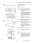
Specifications
å System
• CPU: 80386SX-40 MHz, 80486SLC-33 MHz
• Bus interface: ISA (PC/AT) bus
• System performance:
51.9 MHz with an 80386SX-40 MHz CPU
• Data bus: 16 bit
• DMA channels: 7
• Interrupt levels: 15
• Processing ability: 32 bit
• Bus speed: 8 MHz
• Chipset: ALI M1217-40
• Real-time clock/calendar:
Uses Dallas DS-12887 RTC or equivalent chip and quartz oscillator,
powered by a lithium battery for 10 years of data retention
å Memory
• RAM memory: 1 MB to 16 MB
Uses 256Kx9 (SIMM-256-7), 1Mx9 (SIMM-1000-7) or 4Mx9
(SIMM-4000-7) SIMMs with access time of 70 nsec. or less
• Shadow RAM memory: Support for system and video BIOS of up
to 256 KB in 32 KB blocks
å I/O
• IDE hard disk drive interface: Supports up to two IDE (AT bus)
hard disk drives. Can be enabled/disabled
• Floppy disk drive interface:
Supports up to two floppy disk drives, 5.25” (360 KB and 1.2 MB)
and/or 3.5” (720 KB, 1.44 MB and 2.88 MB). Can be enabled/
disabled
Chapter 1 Hardware Configuration
3
• Bi-directional parallel port: Configurable to LPT1, LPT2, LPT3 or
disabled. Standard female DB-25 connector provided
• Serial ports: Dual RS-232 serial ports with 16C550 compatible
UARTs (16-byte FIFO for speeds up to 115 Kbps). Ports can be
individually configured as COM1, COM2 or disabled
å Industrial features
• Watchdog timer:
The timeout interval is software programmable and can be set
between 2 to 30 sec.. Your program uses hex 043 and 443 to control
the watchdog and set the timeout period
• PC/104 Expansion:
A 64- and 40-pin, 16-bit bus connector for optional PC/104 modules
such as a Flash/RAM/ROM disk module and/or Flat-panel/CRT
VGA module
• Keyboard connectors: A 6-pin mini-DIN keyboard connector is
located on the mounting bracket for easy access. An external
keyboard adapter is also included. An on-board keyboard pin header
connector is also available.
å General
• Max power required: + 5 V @ 1.2 A
• Power supply voltage: +5 V (4.75 V to 5.25 V), +12 V, -12 V
• Operating temperature: 32 to 140oF (0 to 60oC)
• Size: 7.3" (L) x 4.8" (W) (185 mm x 122 mm)
• Weight: 0.55 lbs. (250g)
• EMI: Pending
• MTBF: Pending
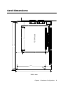
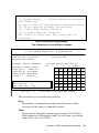
Locating components
This section identifies the location of the card's major components. It
also includes a list of the function of each of the card jumpers. The
figure on the following page gives an overall view of the card.
4
SBC-350A User's Manual
MAX211
CN5
ODIN
J6 CN13 COM1
COM2
CN12
CN6
OEC12C887
CN9
CN4
24MHz
ADVRNCED
MICRO
DEVICES
Am386
AMIKEY T M -2
AMIBIOS
SMC
FDC37C665
AMERICAN MEGATRENDS
386SX BIOS
MAX211
CN7,8
ALI
M1217
TMS X - 4 0
J5,4,3,2
CN3
14.318
SIMM
Sockets
J1
CN1
CN2
SBC-350A HALF-SIZE ISBC PC-386SX-40 REV:.A1
SBC-350A PCB Layout
Chapter 1 Hardware Configuration
5
Jumpers and connectors
Connectors on the board link it to external devices such as hard disk
drives, a keyboard or PC/104 modules. In addition, the board has a
number of jumpers which you use to configure it for your application.
The table below lists the function of each of the board jumpers and
connectors. Later sections in this chapter give instructions on setting
jumpers and detailed information on each jumper setting. Chapter 3
gives instructions for connecting external devices to your card.
Jumpers and Connectors
Number
J1
Function
Reset switch
Page
19
J2,3,4,5
CPU clock and AT clock select
8
J6
Display type - mono, color
8
CN1
Power LED and Keylock
19
CN2
Hard disk driver activity LED
19
CN3
HDD connector
17
CN4
FDD connector
16
CN5
Parallel/printer connector
18
CN6
Keyboard connector
18
CN7/8
PC/104 expansion connector
43
CN9
SBC Power connector
20
CN10
COM1, RS-232 serial port
20
CN11
COM2, RS-232 serial port
20
CN12
Keyboard connector (6-pin mini DIN)
18
CN13
External speaker connector
21
SIMM memory modules
On the left end of the card (away from the mounting bracket) are the
four SIMM (Single In-line Memory Module) sockets which hold the
card’s DRAM memory. If you ordered DRAM SIMMs along with your
card, the SIMMs may already be installed. If not, you should install
them as described in Appendix B.
6
SBC-350A User's Manual
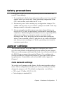
Safety precautions
Follow these simple precautions to protect yourself from harm and
your PC from damage.
1. To avoid electric shock always disconnect the power from your PC
chassis before you work on it. Don’t touch any components of the
CPU card or other cards while the PC is on.
2. Disconnect power before making any configuration changes. The
sudden rush of power as you connect a jumper or install a card may
damage sensitive electronic components.
3. Always ground yourself to remove any static charge before you
touch your CPU card. Be particularly careful not to touch the chip
connectors. Modern integrated electronic devices, especially CPUs
and memory chips, are extremely sensitive to static electric
discharges and fields. Keep the card in its anti-static packaging
when it is not installed in the PC and place it on a static dissipative
mat when you are working on it. Wear a grounding wrist strap for
continuous protection.
Jumper settings
This section tells how to set the jumpers to configure your card. It
gives the card default configuration and your options for each jumper.
After you set the jumpers and install the card, you will also need to run
the BIOS Setup program (discussed in Chapter 5) to configure the
serial port addresses, floppy/hard disk drive types and system operating parameters. Connections, such as hard-disk cables, appear in
Chapter 3.
Card default settings
We set the card’s jumpers at the factory for the most popular configuration. If this configuration matches your needs, you may not need to
change the jumpers at all. The default configuration is as follows:
• CPU clock: 33 MHz. (J2, J3, J4, J5)
• Color display is attached (J6)
Chapter 1 Hardware Configuration
7
How to set jumpers
You configure your card to match the needs of your application by
setting jumpers. A jumper is the simplest kind of electric switch. It
consists of two metal pins and a small metal clip (often protected by a
plastic cover) that slides over the pins to connect them. To “close” a
jumper you connect the pins with the clip. To “open” a jumper you
remove the clip. Sometimes a jumper will have three pins, labeled 1, 2
and 3. In this case you would connect either pins 1 and 2 or 2 and 3.
You may find pair of needle-nose pliers useful for setting the jumpers.
If you have any doubts about the best hardware configuration for your
application, contact your local distributor or sales representative
before you make any changes.
CPU clock and AT clock select (J2, J3, J4, J5)
J2, J3, J4, and J5 are used to adjust the CPU clock and AT clock. Set
the CPU clock according to the base CPU speed. The default setting is
33 MHz.
CPU clock and AT clock select (J2, J3, J4, J5)
25 MHz
¡ ¡
¡ ¡
¡ ¡
20 MHz
¡ ¡
¡ ¡
¡ ¡
¡ ¡
J5
¡ ¡
¡ ¡
¡ ¡
J4
¡ ¡
¡ ¡
¡ ¡
J3
¡ ¡
33 MHz
¡ ¡
40 MHz
¡ ¡
J2
Display type (J6)
This jumper sets the display adapter type attached to your card. If you
are using a monochrome LCD or EL screen which uses a CGA, EGA,
VGA or other color display adapter, set J6 to color.
Monochrome
Closed
Color
Open (default)
8
SBC-350A User's Manual
178.00
80.65
19.00
98.50
D4x4
19.50
122.00
185.00
73.66
PC/104 Module
26.00
Card Dimensions
Unit = mm
Chapter 1 Hardware Configuration
9
10
SBC-350A User's Manual
CHAPTER
Installation
2
This chapter gives a general procedure for
installing your CPU card into an PC
chassis with an AT-compatible passive
backplane. For specific instructions,
consult the user’s manual for your chassis.
Chapter 2 Installation
11
Initial Inspection
Before you begin installing your card, please make sure that the
following materials have been shipped:
• 1 SBC-350A CPU card
• 1 6-pin mini-DIN keyboard adapter
• 1 Hard disk drive (IDE) interface cable (40 pin)
• 1 Floppy disk drive interface cable (34 pin)
• 1 Parallel port adapter (26 pin) kit
• PC/104 Expansion connector converter (pin headers)
• PC/104 Module mounting supports
If any of these items are missing or damaged, contact your distributor or sales representative immediately.
We carefully inspected the SBC-350A mechanically and electrically before we shipped it. It should be free of marks and scratches
and in perfect working order on receipt.
As you unpack the SBC-350A, check it for signs of shipping
damage (damaged box, scratches, dents, etc.). If it is damaged or it
fails to meet specifications, notify our service department or your
local sales representative immediately. Also notify the carrier.
Retain the shipping carton and packing material for inspection by
the carrier. After inspection we will make arrangements to repair or
replace the unit.
Warning! Always completely disconnect the power cord
from your chassis whenever you are working on
it. Do not make connections while the power is
on, sensitive electronic components can be
damaged by the sudden rush of power. Only
experienced electronics personnel should open
the PC chassis.
12
SBC-350A User's Manual
Caution!
Always ground yourself to remove any static
charge before touching the CPU card. Modern
electronic devices are very sensitive to static
electric charges. Use a grounding wrist strap at
all times. Place all electronic components in a
static-dissipative surface or static-shielded bag
when they are not in the chassis.
Before you begin installation, double check the jumper settings for
the card (described in Chapter 1). This could save you a lot of
troubleshooting time later. If you are not sure about the proper
setting, contact your local distributor or sales representative.
Install your CPU card as follows:
1. Remove power from the chassis and disconnect all power
cords. Follow all power-down procedures outlined in your
chassis user’s manual.
2. Remove the chassis cover, then detach the card hold-down
bracket. This bracket stretches across the top of each circuit
card to hold it securely in place.
3. Locate a free slot in the chassis. You can use any 16-bit (double
connector) slot. We suggest that you leave the maximum
amount of space between boards to improve cooling.
4. You may need to remove a block-off cover at the end of the
slot. Unscrew the cover and save the screw for use in Step 6.
5. Align the card square with the card-end guide slot and parallel
to the connector. Slide the card carefully into the connector.
6. Make sure the card is completely seated in the connector. Screw
the card I/O bracket to the case.
After you have installed the CPU card, you will need to attach the
connecting cables as described in the following chapter. When you
are finished installing the CPU card, replace the card hold-down
bracket you removed in Step 2, replace the chassis cover and
power-up your system.
Dimensions for SBC (Single Board Computer) installation appear
on page 9.
Chapter 2 Installation
13
14
SBC-350A User's Manual
CHAPTER
Connecting
peripherals
3
This chapter tells how to connect peripherals, switches and indicators to the SBC350A board. You can access most of the
connectors from at the top of the board
while it is installed in the chassis. If you
have a number of cards installed, or your
chassis is very tight, you may need to
partially remove the card to make all the
connections. When everything is done,
finish installing the card as described in
Chapter 2.
Chapter 3 Connecting peripherals
15
SBC-350A Card Connectors
The following table lists the connectors on the SBC-350A. See
Chapter 1 for help locating the connectors.
SBC-350A Connectors
Component
Label
Reset switch connector
J1
Power LED and Keylock
CN1
HDD LED connector
CN2
HDD (IDE) connector
CN3
FDD connector
CN4
Parallel port
CN5
Keyboard connector
CN6
PC/104 expansion connector
CN7/8
SBC power connector
CN9
COM1 RS-232 serial port
CN10
COM2 RS-232 serial port
CN11
Keyboard connector (6-pin mini DIN)CN12
External speaker connector
CN13
Page
19
19
19
17
16
18
18
43
20
20
20
18
21
The following sections tell how to make each connection. In most
cases you will simply need to connect a standard cable.
Floppy drive connections (CN4)
You can attach up to two floppy disk drives to the SBC-350A's onboard controller. You can use any combination of 5.25"
(360 KB and 1.2 MB) and/or 3.5" (720 KB, 1.44 MB and 2.88
MB) drives.
The card comes with a 34-pin daisy-chain drive connector cable.
On one end of the cable is a 34-pin flat-cable connector. On the
other end are two sets of floppy disk drive connectors. Each set
consists of a 34-pin flat-cable connector (usually used for 3.5"
drives) and a printed-circuit-board connector (usually used for
5.25" drives). You can use only one connector in each set. The set
on the end (after the twist in the cable) connects to the A: floppy.
The set in the middle connects to the B: floppy.
16
SBC-350A User's Manual
Attach the single 34-pin flat-cable connector to CN4 on the CPU
card. For help finding the connector, see Chapter 1. Wire number 1
on the cable is red or blue, the other wires are gray. Make sure that
the red wire corresponds to pin one on the connector (on the right
side).
Connect the A: floppy drive to the connector set on the other end
of the cable. If you are connecting a 5.25" floppy drive, line up the
slot in the printed-circuit-board (golden fingers) with the blockedoff part of the cable connector.
If you are connecting a 3.5" floppy drive, you may have trouble
determining which pin is number one. Look for a number printed
on the circuit board indicating pin number one. Also, the connector
on the floppy drive connector may have a slot. When the slot is up,
pin number one should be on the right. Check the documentation
that came with the drive for more information.
Next, if you desire, connect the B: floppy drive to the connectors in
the middle of the cable as described above.
IDE hard drive connections (CN3)
You can attach two IDE (Integrated Device Electronics) hard disk
drives to the SBC-350A internal controller. The card comes with a
40-pin flat-cable piggyback cable. This cable has three identical
40-pin flat-cable connectors.
Wire number 1 on the cable is red or blue, the other wires are gray.
Connect one end to connector CN3 on the CPU card. Make sure
that the red wire corresponds to pin one on the connector (on the
right side). See Chapter 1 for help finding the connector.
Unlike floppy drives, IDE hard drives can connect in either
position on the cable. If you install two drives, you will need to set
one as the master and one as the slave. You do this using jumpers
on the drives. If you use just one drive, you should set it as the
master. See the documentation that came with your drive for more
information.
Chapter 3 Connecting peripherals
17
Connect the first hard drive to the other end of the cable. Wire one
on the cable should also connect to pin one on the hard drive
connector. You may have difficulty determining the pin number.
Look for a number printed on the drive circuit board. Also, the
connector on the floppy drive connector may have a slot. When the
slot is up, pin number one should be on the right. Check the
documentation that came with the drive for more information.
Connect a second drive as described above.
Parallel Port (CN5)
You would normally use the parallel port to connect the card to a
printer. The SBC-350A includes an on-board bi-directional parallel
port, accessed through a 26-pin flat-cable connector, CN5. The
CPU card comes with an adapter cable which lets you use a
traditional DB-25 connector. The cable has a 26-pin connector on
one end and a DB-25 connector on the other, mounted on a
retaining bracket. The bracket installs at the end of an empty slot in
your chassis, giving you access to the connector.
To install the bracket find an empty slot in your chassis. Unscrew
the plate that covers the end of the slot. Screw in the bracket in
place of the plate. Next, attach the flat-cable connector to connector CN5 on the CPU card. Wire one of the cable is red or blue, the
other wires are gray. Make sure that wire one connects to pin one
of CN5. Pin one is on the right side of CN5. For help finding the
connector, see the figure on page 5.
Keyboard connectors (CN6, CN12)
The SBC-350A board provides two keyboard connectors. A 5-pin
connector (CN6) supports passive backplane applications. A
second 6-pin mini-DIN connector (CN12) on the card mounting
bracket supports single-board-computer applications. The card
comes with an adapter to convert from the 6-pin mini-DIN connector to a standard DIN connector.
18
SBC-350A User's Manual
External switches and indicators
Next you may want to install external switches to monitor and
control your CPU card. These features are completely optional —
install them only if you need them.
Reset switch (J1)
You can connect an external switch to easily reset your computer.
This switch restarts your computer as if you had turned off the
power then turned it back on. Install the switch so that it closes the
two pins of J1.
Power LED and keylock (CN1)
You can connect an LED to indicate when the CPU card is on. Pin
1 of CN1 supplies power to the LED and Pin 3 is the ground. For
help finding CN1 see the figure on page 5.
You can use a switch (or a lock) to disable the keyboard. In this
state the PC will not respond to any input. This is useful if you
don’t want anyone to change or stop a running program. Simply
connect the switch between Pins 4 and 5 of CN1. The pin assignments for CN1 appear in the following table:
Power LED and Keylock (CN1)
Pin
1
2
3
4
5
Function
LED Power (+5 V)
No Connection
Ground
Keyboard lock
Ground
Hard disk drive LED (CN2)
You can connect a LED to connector CN2 to indicate when the
HDD is active. Marks on the circuit board indicate LED polarity
(the pin on the left is positive).
Chapter 3 Connecting peripherals
19
SBC power connector (CN9)
In single-board-computer (non-passive-backplane) applications
you will need to connect power directly to the SBC-350A board
using connector CN9. This connector is fully compatible with the
standard PC power supply connector (P8). Refer to the following
table for CN9's pin assignments.
SBC Power Connector (CN9)
Pin no. Function
1
Power good
2
+5 V DC
3
+12 VDC
Pin no. Function
4
-12 VDC
5
GND
6
GND
Serial Ports
The SBC-350A offers two RS-232 16C550 compatible serial ports.
These ports let you connect to serial devices (mouse, printers,
modems etc.) or a communication network.
You can select the address for each port or disable it through the
BIOS Advanced Setup program, covered in Chapter 5. The
following are the options for both ports:
Serial Port Setup Options
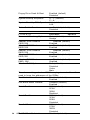
Port
COM1
COM2
Disable
Disable
Address options
3F8
3E8
2F8
2E8
2F8
3F8
The card mounting bracket holds the serial port connectors. This
lets you connect and disconnect cables after you install the card.
The DB-9 connector on the top of the bracket is the COM1 RS-232
port. The second DB-9 connector is the COM2 RS-232 port. The
following section tells how to make RS-232 connections.
20
SBC-350A User's Manual
RS-232 connections (CN10, CN11)
Different devices implement the RS-232 standard in different ways.
If you are having problems with a serial device, be sure to check
the pin assignments for the connector. The following table shows
the pin assignments for the card's RS-232 port:
RS-232 Connector Pin Assignment
Pin no.
1
2
3
4
5
6
7
8
9
Signal
DCD
RX
TX
DTR
GND
DSR
RTS
CTS
RI
External speaker connector (CN13)
If the SBC-350A is installed into an enclosure, an external speaker
can be connected to CN13.
External Speaker Connector (CN13)
Pin no.
1
2
3
4
Signal
+5 V
Speaker out
Speaker out
Speaker out
Now that you have made all the required external connections, you
can close up your chassis (as described in Chapter 2). If you are
installing any other cards, do it now. You can then power up your
system as described in the next chapter.
Chapter 3 Connecting peripherals
21
22
SBC-350A User's Manual
CHAPTER
Power-up
4
After you have set the jumpers (Chapter 1),
installed SIMMs (Appendix B), installed the
card (Chapter 2) and made all external
connections (Chapter 3), you are ready to
power-up your system.
Chapter
4
Power-up
2 3
Startup Procedure
Follow the startup procedure outlined in the manual for your
chassis.
When you start your system, the BIOS will test the hardware and
check the system configuration against the values stored in its
CMOS memory.
Since this is the first time you are starting up, the BIOS will display
an error message stating that the configuration does not match the
stored values. You should then run the BIOS setup program as
described in Chapter 5.
If the BIOS hardware diagnostic tests fail, you may see an error
message on the screen describing the problem. If the BIOS found a
problem early in the tests, you will need to determine the BIOS
POST (Power On Self Test) results by counting beeps or using a
POST card.
The most common source of problems is incorrect jumper settings.
Double check your settings (Chapter 1) and restart the system.
There are three methods you can use to restart your system after it
is turned on:
1. Switch the power off, then on again
2. Reboot the system. Using the keyboard, simultaneously press
the CTL, ALT and DEL keys
3. Depress the optional reset switch
Use of each of these methods will erase data from the system RAM
memory. If you can, save any data stored in memory to a hard or
floppy disk before you reset your system.
24
SBC-350A
User's
Manual
CHAPTER
BIOS diagnostics
and SETUP
5
This chapter describes the card’s diagnostic tests and how to set BIOS configuration data.
Chapter 5 BIOS diagnostics and setup
25
POST (Power On Self Tests)
Whenever you start up your system, the CPU card runs a series of
programs stored in an on-board ROM chip. These programs are
divided into two stages:
System test and initialization
These routines test and initialize board hardware. If the routines
encounter an error in during the tests, you will either hear a few
short beeps or see an error message on the screen. There are two
kinds of errors: fatal and non-fatal. The system can usually
continue the boot up sequence with non-fatal errors. Non-fatal
error messages usually appear on the screen along with the
following instructions:
press <F1> to RESUME
Write down the message and press the F1 key to continue the
bootup sequence. Non-fatal error messages appear in Appendix E.
If the routines encounter a fatal error, they will stop the tests and
output a message indicating which test failed. If the fatal error
comes before the screen device initializes, the card will indicate the
error code through a series of beeps.
System configuration verification
These routines check the current system configuration against the
values stored in the card’s CMOS memory. If they don’t match, the
program outputs an error message. You will then need to run the
BIOS setup program to set the configuration information in
memory.
There are three situations in which you will need to change the
CMOS settings:
1. You are starting your system for the first time
2. You have changed the hardware attached to your system
26
SBC-350A User's Manual
3. The CMOS memory has lost power and the configuration
information has been erased.
The SBC-350A’s CMOS memory has integral lithium battery
backup. The battery backup should last ten years in normal service,
but when it finally runs down, you will need to replace the complete unit. Contact your sales representative or distributor for
details.
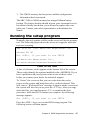
Running the setup program
Normally, the only routine visible on the screen will be the memory
test. The following figure shows the screen as it appears while the
tests are occurring.
AMI BIOS(c) 1993 American Megatrends Inc.,
xxxxxx KB OK
Hit <DEL>, If you want to run SETUP
(c)American Megatrends Inc.,
xx-xxxx-xxxxxx-xxxxxxx-xxxxxx-xxxx
Power On Self Tests
A line of reference codes appears at the bottom left of the screen.
These codes identify the options installed in the AMI BIOS. If you
have a problem with your system, make a note of these codes
before you contact your dealer for technical support.
To “freeze” the screen so that you can write down the codes,
power-on the system and hold down a key on the keyboard. This
will cause a “Keyboard Error” message to appear on the screen and
the system will wait for you to press the <F1> key. After you copy
down the line, you can then press <F1> to continue the boot
procedure. After the POST routines are complete, the following
message appears:
Hit <DEL>, If you want to run SETUP
Press the <DEL> key to access the BIOS setup program. The
following screen will then appear.
Chapter 5 BIOS diagnostics and setup
27
BIOS Setup Main Menu
You use the following keys to control the BIOS SETUP program:
ESC: Exit to previous screen
ARROW KEYS: Moves the cursor to highlight the desired
configuration option
PAGEUP/PAGEDOWN/CTRL-PAGEUP/CTRL-PAGEDOWN:
Cycles through the configuration options for the highlighted
feature. If there are less than ten available options, the CtrlPageUp and Ctrl-PageDown keys function the same as the
PageUp and PageDown keys.
F1: Displays a help screen for selected feature.
F2/F3: Changes background and foreground colors.
F5: Retrieves the values which were resident when the current
setup session was started. These values will be CMOS values if
the CMOS was uncorrupted at the start of the session, or they
will be the BIOS Setup default values.
F6: Loads all features in the Advanced CMOS Setup with the
BIOS Setup defaults.
F7: Loads all features in the Advanced CMOS Setup with the
Power-On defaults (the values in the CMOS when the system
was started).
F10: Saves all changed made to Setup and exits program.
Standard CMOS Setup
Standard CMOS setup configures options that most users will need
to change. Highlight Standard CMOS Setup in the main screen
and press <ENTER>.
A warning message appears (shown below) whenever you select
either Standard CMOS Setup, Advanced CMOS Setup or Advanced Chipset Setup from the main screen. Simply press any key
to continue or ESC to abort.
28
SBC-350A User's Manual
Improper Use of Setup may Cause Problems!!
If System Hangs,.....Enter Setup by pressing
the <DEL> key
Do any of the following After Entering Setup
(i) Alter Option to make System Work
(ii) Load BIOS Setup Defaults
(iii) Load Power-On Defaults
Hit <ESC> to Stop now, Any other Key to
continue
BIOS Setup Warning Message
The following screen will then appear:
BIOS Setup Program - Standard CMOS SETUP
(C) 1993, American Megatrends Inc., All Rights Reserved
Date (mn / date / year): Tue, Jan 01 1991
Time (hour / min / sec): 09:39:06
Daylight Saving: Disabled
Hard disk C: type: 47= USER TYPE
Hard disk D: type:Not Installed
Floppy drive A: :1.2MB, 51/4"
Floppy drive B: :Not Installed
Primary display :Monochrome
Keyboard
:Installed
Month: Jan, Feb,...........Dec
Date : 01, 02, 03..........31
Year : 1901, 1902.........2099
Esc = Exit,
Base memory: 640KB
Ext. memory: 0KB
Cyln Head WPCom LZone Sect Size
642
8
0
0
17 43MB
Sun Mon Tue Wed Thu Fri
30
31
1
Sat
2
3
4
5
6
7
8
9
10
11
12
13
14
15
16
17
18
19
20
21
22
23
24
25
26
27
28
29
30
31
1
2
3
4
5
6
7
8
9
¬ ® ¯ -= Select, F2/F3 = Color, PgUp/PgDn = Modify
This screen lets you set following features:
Date:
System date. A prompt box at the lower left corner of the
screen gives the range of allowable values.
Time:
System clock. Hour first, minute then second. Uses 24 hour
clock format (for PM numbers add 12 to the hour: you would
enter 4:30 p. m. as 16:30:00)
Chapter 5 BIOS diagnostics and setup
29
Daylight Savings: Disabled or Enabled
Hard Disk C: and Hard Disk D:
The BIOS supports 46 standard hard disk sizes and layouts. If
your hard disk matches one of these types (shown below),
highlight the number blank (for the appropriate drive, C: or D:)
and press <PgDn> until the correct number appears. If the
BIOS does not support your hard disk, select disk type 47 and
enter each of the specifications into the blank (e. g. number of
cyln.). You can get these numbers from a label on your disk
drive or from the documentation that came with the drive. After
you have set up drive C:, you can then set up drive D:. If you
have no drive D:, select Not Installed.
Hard Disk Types
Type
Size
1
2
3
4
5
6
7
8
9
10
11
12
13
14
16
17
18
19
20
21
22
30
Cyln
Head
WPcomp
LZone Sect
306
615
615
940
940
615
462
733
900
820
855
855
306
733
612
977
977
1024
733
733
733
4
4
6
8
6
4
8
5
15
3
5
7
8
7
4
5
7
7
5
7
5
128
300
300
512
512
65535
256
65535
65535
65535
65535
65535
128
65535
0
300
65535
512
300
300
300
17
17
17
17
17
17
17
17
17
17
17
17
17
17
17
17
17
17
17
17
17
SBC-350A User's Manual
305
615
615
940
940
615
511
733
981
828
855
855
319
733
663
977
977
1023
732
732
733
10 MB
20 MB
31 MB
62 MB
47 MB
20 MB
31 MB
30 MB
112 MB
20 MB
35 MB
50 MB
20 MB
43 MB
20 MB
41 MB
57 MB
60 MB
30 MB
43 MB
30 MB
23
306
4
0
336
Type
Size
24
25
26
27
28
29
30
31
32
33
34
35
36
37
38
39
40
41
42
43
44
45
46
47
Cyln
Head
WPcomp
LZone Sect
925
925
754
754
699
823
918
1024
1024
1024
612
1024
1024
615
987
987
820
977
981
830
830
917
1224
user type
7
9
7
11
7
10
7
11
15
5
2
9
8
8
3
7
6
5
5
7
10
15
15
0
65535
754
65535
256
65535
918
65535
65535
1024
128
65535
512
128
987
987
820
977
981
512
65535
65535
65535
17
17
17
17
17
17
17
17
17
17
17
17
17
17
17
17
17
17
17
17
17
17
17
925
925
754
754
699
823
918
1024
1024
1024
612
1024
1024
615
987
987
820
977
981
830
830
918
1223
17
10 MB
54 MB
69 MB
44 MB
69 MB
41 MB
68 MB
53 MB
94 MB
128 MB
43 MB
10 MB
77 MB
68 MB
41 MB
25 MB
57 MB
41 MB
41 MB
41 MB
48 MB
69 MB
114 MB
152 MB
Note that the user definition entry (47) lets you a test on a disk
drive not defined in ROM. The USER definition entry is valid
only during the period that the test is performed.
The following chart shows the meaning of each of the hard disk
parameters:
Hard disk parameters
Type:
Cyln:
This is the number designation for a drive with
certain identification parameters.
This is number of cylinders found in the specified
drive type.
Chapter 5 BIOS diagnostics and setup
31
Heads:
This is the number of heads found in the specified
drive type.
WPcom:
WPcom is the read delay circuitry which takes into
account the timing differences between the inner
and outer edges of the surface of the disk platter.
The number designates the starting cylinder of the
signal.
LZone is the landing zones of the heads. This
number determines the cylinder location where the
heads will normally park when the system is shut
down.
The number of sectors per track
This is the formatted capacity of the drive based on
the following formula:
(# of heads) x (# of cylinders) x (# of sectors) x
(512 bytes/sec.)
L-Zone:
Sectors:
Size:
Floppy Drive A: and Floppy Drive B:
The BIOS supports any combination of 3.5" (720 KB
1.44 MB and 2.88MB) and 5.25" (360 KB and 1.2 MB) floppy
disks. If you have no floppy disk installed, select Not Installed.
Primary Display:
Select the type of display you have connected. Options are:
Monochrome, Color 40x25, VGA/PGA/EGA, Color 80x25 and
Not Installed. You might use the Not installed option for a
network file server.
Keyboard:
Options are Installed or Not Installed.
Note: If you are running your system on a non-dedicated file
server, and you do not want the AMI BIOS to report any
keyboard, video or floppy disk drive errors during POST, set
the AMI BIOS Keyboard, Primary display and floppy disk
features to “Not Installed.”
Advanced CMOS Setup
Advanced CMOS Setup controls system settings. Adjusting these
parameters may improve system performance, but make a note of
the original settings before you make any changes. Some combinations of settings may cause your system to crash or become
32
SBC-350A User's Manual
unreliable.
From the main menu highlight the Advanced CMOS Setup option
and press <ENTER>. Press any key to clear the warning screen.
Features
The following chart lists card settings which you can change in
Advanced CMOS Setup. It lists the default value for each setting.
This screen has several help screens, accessed by pressing the
<F1> key, which display setting options.
Help Screen Options
Feature
Type Rate Programming
Type Rate Delay (msec)
1000
Type Rate (Chars/sec)
20,
Available options
Disabled (default)
Enabled
250, 500 (default), 750,
6, 8, 10, 12, 15 (default),
24, 30
Disabled (default)
Enabled
Memory Test Tick Sound
Enabled (default)
Disabled
Memory Parity Error Check
Enabled (default)
Disabled
Hit <DEL> Message Display
Enabled (default)
Disabled
Hard Disk Type 47 RAM Area 0:300 (default)
DOS 1KB
This setting determines where in memory the hard disk information is stored when you select hard disk type 47. If you
disable BIOS Shadow RAM, the Hard Disk Type 47 parameter
table will use regular RAM. There are two options, 0:300 (lower
system RAM) and DOS 1 KB (the top 1KB of 640 KB base
memory).
Wait for <F1> if Any Error
Enabled (default)
Disabled
System Bootup Num Lock
On (default)
Off
Above 1MB Memory Test
Chapter 5 BIOS diagnostics and setup
33
Floppy Drive Seek At Boot
System Bootup Sequence
System Boot Up CPU Speed
Turbo Switch Function
F e a t u r e
Password Checking Option
34
Enabled (default)
Disabled
A:, C: (default)
C:, A:
High (default)
Low
Enabled (default)
Disabled
Available
options
Setup (default)
Always
Adapter ROM Shadow
Disabled (default)
C800,32K
Enabled
Adapter ROM Shadow
Disabled (default)
D000,32K
Enabled
Adapter ROM Shadow
Disabled (default)
D800,32K
Enabled
Adapter ROM Shadow
Disabled (default)
E000,32K
Enabled
Adapter ROM Shadow
Disabled (default)
E800, 32K
Enabled
Shadow RAM Option
Both (default)
Disabled
Video
Main
The above settings shadow ROMs on plug-in cards. You will
need to know the addresses of the ROMs.
BootSector Virus Protection
Disabled (default)
Enabled
IDE Block Mode Transfer
Disabled (default)
Enabled
Serial Port 1
3F8H (default)
2F8H
3E8H
Disabled
Serial Port 2
2F8H (default)
3F8H
2E8H
Disabled
Parallel Port
378H (default)
278H
3BCH
Disabled
SBC-350A
ParallelUser's
Port Manual
bi-direction
Disabled (default)
Enabled
Enabled (default)
Disabled
Enabled (default)
Disabled
IDE Controller
Floppy Controller
After you have made your configurations changes, press <ESC> to
return to the main menu.
Advanced CHIPSET Setup
Advanced CHIPSET Setup controls the ALI-1217-40 chipset's
configuration registers. Adjusting these parameters may improve
system performance. Should you make any changes, make sure you
note the original settings for future reference. Certain combinations
of system settings can cause conflicts and may result in a system
crash or unreliable operation.
From the main menu, highlight the Advanced CHIPSET Setup
option, and press <ENTER>. Press any key to clear the warning
screen.
Features
The following chart lists card settings which you can change in
Advanced CHIPSET Setup. It lists the default value for each
setting. This screen has several help screens, accessed by pressing
the <F1> key, which display setting options.
Help Screen Options
Feature
Burst Memory Access Wait
Memory Access Wait Time
RAS Time Out
CAS Precharge Time Wait
RAS Active Time Wait
Fast RAS Precharge Time
Available options
Disable (default)
Enable
Disable (default)
Enable
Disable
Enable (default)
Disable (default)
Enable
Disable (default)
Enable
Disable (default)
Chapter 5 BIOS diagnostics and setup
35
Enable
16-bit ISA Cycle Insert Wait
Slow Refresh
Refresh Type
IO Recovery
On Chip I/O Recovery
I/O Recover Period Define
ns/step
0 w/s (default)
1 w/s
Disable
Enable (default)
CAS/RAS (default)
RAS only
Disable (default)
Enable
Disable (default)
Enable
0 (default) ....3750ns, 250
Auto Configuration with BIOS Defaults
This main menu option loads the system default values stored in
the BIOS ROM at the factory.
Auto Configuration with Power-On Defaults
This main menu option loads the settings stored in the CMOS
memory when you turned on your system. If your system behaves
erratically, you can use this feature to check for incorrect settings.
Auto Detect Hard Disk
This option simplifies the hard disk drive configuration by automatically configuring the system to your HDD
Hard Disk Utility
This option lets you perform low-level hard disk drive preparation
before you use the DOS FDISK or FORMAT utilities. All of its
functions are destructive to existing data on the disk drive.
Most IDE hard drives come preformatted from the factory, so you
will probably only need these utilities if your hard disk develops
bad sectors or ages and needs to have the formatting information
refreshed.
Write to CMOS and Exit/Do not Exit
After you have made your configuration changes, select Write to
CMOS and Exit. If you decide you want to abandon the changes
you have made, select Do not Write to CMOS and Exit.
36 SBC-350A User's Manual
The BIOS will then perform a memory test, and attempt to boot
APPENDIX
A
Programming the
watchdog timer
The SBC-350A is equipped with a 15
level watchdog timer that resets the CPU
if processing comes to a standstill for
whatever reason. The time-out interval is
software programmable for periods of 2 to
30 seconds. This feature ensures system
reliability in industrial stand-alone and
unmanned environments.
Appendix A Programming the watchdog timer
37
Introduction
To utilize the watchdog timer, you must write a program which
writes to I/O port address 443 (hex) at regular intervals. The first
time your program writes to the port, it enables the watchdog timer
and sets the time-out interval. After that your program must write
to the port at time intervals less than the time-out interval, otherwise the watchdog timer will activate and reset the CPU. When you
want to disable the watchdog timer, your program should write I/O
port 043 (hex).
If CPU processing comes to a standstill because of EMI or a
software bug, your program's signals to I/O port address 443 to the
timer will be interrupted. The timer will then automatically reset
the CPU and data processing will continue normally.
Programming
You must write your program so that it write to I/O port address
443 at an interval shorter than the timer’s preset interval. The
timer’s interval has a tolerance of ±5%, so you should program an
instruction that will refresh the timer before a time-out occurs. The
following steps illustrate how you might program the watchdog
timer.
Step1
Write to I/O port 443 (Hex) and designate a time-out
interval. This will enable the watchdog and set-up it's
time-out interval
Step2
Write to I/O port 043 (Hex) and any random value. This
will in turn disable the watchdog timer.
The watchdog's time-out interval can be set at 15 levels between 2
and 30 seconds. The following table shows the Hex values for the
appropriate time-out intervals:
38
SBC-350A User's Manual
Watchdog Timer Delay Values
Delay Time
(Hex)
0~2
2~4
4~6
6~8
8 ~ 10
10 ~ 12
12 ~ 14
14 ~ 16
Value (Hex)
Delay Time
Value
E
D
C
B
A
9
8
7
16
18
20
22
24
26
28
6
5
4
3
2
1
0
~
~
~
~
~
~
~
18
20
22
24
26
28
30
The following demo program illustrates the programming steps
required to enable, set the time-out interval and disable the
watchdog timer.
#include<stdio.h> #include<dos.h> #include <conio.h> #include
<time.h> #include<graphics.h> void mydelay(void);
/* MAIN PROGRAM */ void main(void) {
unsigned int dog=0,
run_time=0;
char inkey;
clrscr();
gotoxy(15, 6);printf(“AAEON TECHNOLOGY, INC.”);
gotoxy(15, 7);printf(“WATCHDOG TIMER TEST & DEMO
PROGRAM”);
gotoxy(15, 9);printf(“Please setup watchdog delay
time:(2 Sec-30 Sec)”);
/* Set watchdog timer time-out interval */
scanf(“%2d”,&dog);
/* Input watchdog timer timeout interval (Sec) */
dog=dog/2;
/* Convert time-out interval
to designated Hex */
dog=15-dog;
outportb(0x443,dog);
/* Enable watchdog timer */
/* Setup screen display format */
gotoxy(15,11);printf(“Now enable watchdog!”);
gotoxy(15,12);printf(“You can put keyboard reset or
disable watchdog.”);
gotoxy(15,13);printf(“
[1].Reset watchdog.”);
gotoxy(15,14);printf(“
[2].Disable watchdog.”);
gotoxy(15,15);printf(“
[3].Return to O.S.”);
/* Read key pressed */
Appendix A Programming the watchdog timer
39
while(1){
if(kbhit()){
inkey=getch();
switch(inkey){
case ‘1’: /* Reset Watchdog timer */
gotoxy(15,11);printf(“Now enable
watchdog timer!”);
outportb(0x443,dog);
run_time=0;
break;
case ‘2’: /* Disable Watchdog timer */
gotoxy(15,11);printf(“Now disable
watchdog timer!”);
outportb(0x43,dog);
break;
case ‘3’: /* Disable Watchdog timer & return to
DOS */
outportb(0x43,dog);
return;
default : break;
}
}
mydelay();
run_time=run_time+1;
/* Display time elapsed */
gotoxy(45,11);printf(“%2d.%1d sec”,run_time/
10,run_time%10);
}
}
/* USER FUNCTION LIBRARY */ void mydelay(void) /*
Delay program: */ /* Delay 109.89ms (18.2Hz*2) */ {
clock_t start,end;
start=clock();
end=start;
while((end-start)<2){
end=clock();
}
}
40
SBC-350A User's Manual
APPENDIX
Upgrading
B
This appendix gives instructions for
increasing the capabilities of your CPU
card. It covers:
• DRAM memory installation (SIMMs)
• CPU upgrading
• Installing PC/104 modules
Appendix B Upgrading
41
Installing DRAM (SIMMs)
You can install anywhere from 1 MB to 16 MB of on-board
DRAM memory using 256 KBx9, 1 MBx9 or 4 MBx9 SIMMs
(Single In-line Memory Modules). Access time should be 70 ns or
less.
Memory installs in one bank composed of four SIMM sockets. See
the figure on page 5 for help identifying the banks. You must fill all
four sockets, and all SIMMs must be of the same capacity, i. e. you
cannot mix 256 KB SIMMs with 1 MB SIMMs. The following
table shows the memory size for different SIMM capacities:
System memory size
1 MB
4 MB
16 MB
SIMM size and number
256 KB x 4 pcs
1 MB x 4 pcs
4 MB x 4 pcs
The procedure for installing SIMMs appears below. Please follow
these steps carefully.
1. Locate the CPU card’s memory banks, shown in the figure on
page 5.
2. Install the SIMM cards. Install each SIMM so that its chips face
away from the CPU and its gold pins point down into the
SIMM socket.
3. Slip each SIMM into a socket at a 45 degree angle and carefully fit the bottom of the card against the connectors.
4. Gently push the SIMM into a perpendicular position until the
clips on the ends of the SIMM sockets snap into place.
5. Check to ensure that each SIMM is correctly seated and all
connector contacts touch. The SIMM should not move around
in its socket.
42
SBC-350A User's Manual
CPU upgrading
This section tells how to upgrade the card's CPU. You can upgrade
your SBC-350A to a higher powered 486SLC-33 CPU at any time.
Simply remove the old 386SX CPU, install the new 486SLC-33
CPU and short/open the appropriate solder pads for the CPU type
and speed.
1. Disconnect power from the chassis and remove the CPU card.
Follow the instructions in the user's manual for your chassis.
You will also need to disconnect everything you connected in
Chapter 3, Connections.
2. If you are upgrading the CPU, remove any existing CPU from
the card. (See Chapter 1 for help locating the CPU position.)
3. Solder the new CPU onto the SBC-350A. Follow the instructions that came with the CPU.
4. Using a soldering iron, not too hot!, solder the pads CP1, CP2,
CP3, CP6 and CP7 open or closed. These pads will be open/
closed depending on the type of CPU installed. The following
table refers:
CP Configurations
CPU Type
386SX-40
486SLC-33
Open
CP1
Open
CP2
Open
Short
CP3
Open
Short
CP6
Open
Short
CP7
Short
Short
5. Reinstall the CPU card according to the instructions in
Chapter 2.
Installing PC/104 modules
The SBC-350A's PC/104 connectors give you the flexibility to
attach PC/104 expansion modules. These modules perform the
functions of traditional plug-in expansion cards, but save space and
Appendix B Upgrading
43
valuable slots. Modules include:
• PCM-3510
Super VGA Module
• PCM-3520
Flat-panel/CRT VGA Module
• PCM-3410
Super I/O Module
• PCM-3810
Solid-state Disk Module
• PCM-3110
PCMCIA Module
• PCM-3111
Secondary PCMCIA Module
• PCM-3610
Isolated RS-232 and RS-422/485 Module
• PCM-3640
Four port RS-232 Module
• PCM-3660
Ethernet Module
• PCM-3718
30 KHz A/D Module
• PCM-3724
48-channel DIO Module
• PCM-3910
Breadboard Module
To install these modules on the SBC-350A is a quick and simple
operation. The following steps show how to mount the PC/104
modules:
Step1
Remove the SBC-350A from your system paying
particular attention to the safety instructions already
mentioned above.
Step2
Make any jumper or link changes required to the CPU
card now. Once the PC/104 module is mounted you
may have difficulty in accessing these.
Step3
Normal PC/104 modules have "male" connectors and
mount directly onto the main card. However, for
reasons that ensure better bus matching, the connectors
on the SBC-350A and the PC/104 module are both
"female". For this reason you need to plug-in a "malemale" adapter connecter (included with the SBC-350A).
Please refer to the following PC/104 module mounting
diagram on the following page. After this is in place
you then have the correct mounting connector to accept
your PC/104 module.
Step4
44
Mount the PC/104 module onto the CPU card. Do this
by pressing the module firmly but carefully onto the
mounting connectors.
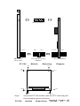
SBC-350A User's Manual
PC/104
Mounting Support
Female
Male
Male
Female
PC/104 Module
PC/104 Mounting
Adaptor
SBC-350A
CPU Card
PC/104
Module
Mounting
3.500
Male
Diagram
3.250
3.775
3.575
3.575
0.200
0.200
0
0.200
3.350
0
Step5
PC/104
3.550
Secure the PC/104 module onto the CPU card using the
four mounting spacers and srews.
module
dimensions
Appendix B Upgrading
(inches
±5
45
%)
46
SBC-350A User's Manual